WO2011052296A1 - プラズマエッチング方法 - Google Patents
プラズマエッチング方法 Download PDFInfo
- Publication number
- WO2011052296A1 WO2011052296A1 PCT/JP2010/065203 JP2010065203W WO2011052296A1 WO 2011052296 A1 WO2011052296 A1 WO 2011052296A1 JP 2010065203 W JP2010065203 W JP 2010065203W WO 2011052296 A1 WO2011052296 A1 WO 2011052296A1
- Authority
- WO
- WIPO (PCT)
- Prior art keywords
- etching
- semiconductor substrate
- temperature
- silicon carbide
- plasma
- Prior art date
- Legal status (The legal status is an assumption and is not a legal conclusion. Google has not performed a legal analysis and makes no representation as to the accuracy of the status listed.)
- Ceased
Links
Images

Classifications
-
- H—ELECTRICITY
- H01—ELECTRIC ELEMENTS
- H01L—SEMICONDUCTOR DEVICES NOT COVERED BY CLASS H10
- H01L21/00—Processes or apparatus adapted for the manufacture or treatment of semiconductor or solid state devices or of parts thereof
- H01L21/02—Manufacture or treatment of semiconductor devices or of parts thereof
- H01L21/04—Manufacture or treatment of semiconductor devices or of parts thereof the devices having potential barriers, e.g. a PN junction, depletion layer or carrier concentration layer
- H01L21/0445—Manufacture or treatment of semiconductor devices or of parts thereof the devices having potential barriers, e.g. a PN junction, depletion layer or carrier concentration layer the devices having semiconductor bodies comprising crystalline silicon carbide
- H01L21/0475—Changing the shape of the semiconductor body, e.g. forming recesses
-
- H—ELECTRICITY
- H01—ELECTRIC ELEMENTS
- H01L—SEMICONDUCTOR DEVICES NOT COVERED BY CLASS H10
- H01L21/00—Processes or apparatus adapted for the manufacture or treatment of semiconductor or solid state devices or of parts thereof
- H01L21/02—Manufacture or treatment of semiconductor devices or of parts thereof
- H01L21/04—Manufacture or treatment of semiconductor devices or of parts thereof the devices having potential barriers, e.g. a PN junction, depletion layer or carrier concentration layer
- H01L21/18—Manufacture or treatment of semiconductor devices or of parts thereof the devices having potential barriers, e.g. a PN junction, depletion layer or carrier concentration layer the devices having semiconductor bodies comprising elements of Group IV of the Periodic Table or AIIIBV compounds with or without impurities, e.g. doping materials
- H01L21/30—Treatment of semiconductor bodies using processes or apparatus not provided for in groups H01L21/20 - H01L21/26
- H01L21/302—Treatment of semiconductor bodies using processes or apparatus not provided for in groups H01L21/20 - H01L21/26 to change their surface-physical characteristics or shape, e.g. etching, polishing, cutting
- H01L21/306—Chemical or electrical treatment, e.g. electrolytic etching
- H01L21/3065—Plasma etching; Reactive-ion etching
-
- H—ELECTRICITY
- H10—SEMICONDUCTOR DEVICES; ELECTRIC SOLID-STATE DEVICES NOT OTHERWISE PROVIDED FOR
- H10D—INORGANIC ELECTRIC SEMICONDUCTOR DEVICES
- H10D62/00—Semiconductor bodies, or regions thereof, of devices having potential barriers
- H10D62/80—Semiconductor bodies, or regions thereof, of devices having potential barriers characterised by the materials
- H10D62/83—Semiconductor bodies, or regions thereof, of devices having potential barriers characterised by the materials being Group IV materials, e.g. B-doped Si or undoped Ge
- H10D62/832—Semiconductor bodies, or regions thereof, of devices having potential barriers characterised by the materials being Group IV materials, e.g. B-doped Si or undoped Ge being Group IV materials comprising two or more elements, e.g. SiGe
- H10D62/8325—Silicon carbide
Definitions
- the present invention relates to a plasma etching method for plasma etching a wide gap semiconductor substrate.
- Si substrate silicon substrate
- GaAs gallium arsenide
- silicon carbide (SiC), gallium nitride (GaN), nitride At least one of boron (B), carbon (C), nitrogen (N) and oxygen (O), such as aluminum (AlN), zinc oxide (ZnO), boron nitride (BN) and boron phosphide (BP) It is comprised including.
- this wide gap semiconductor substrate has a defect that the lattice constant of the crystal is small, that is, the bond between atoms is strong and has excellent physical properties, but the etching process is difficult because of the strong bond between atoms. ing. Therefore, conventionally, as a method for plasma etching such a semiconductor substrate, for example, a plasma etching method for a silicon carbide substrate disclosed in Japanese Patent Application Laid-Open No. 2008-294210 has been proposed.
- a mask forming step of forming a silicon dioxide film (SiO 2 film) having a mask pattern of a predetermined shape on the surface of a silicon carbide substrate, and a mixed gas of SF 6 gas, O 2 gas and Ar gas are used.
- the second etching step of plasma etching the silicon carbide substrate is sequentially performed.
- the ratio of SF 6 gas, O 2 gas and Ar gas is set to a predetermined ratio, and the atmospheric pressure is set to a predetermined value.
- the silicon carbide substrate is heated to 70 ° C. to 100 ° C. , And the ratio a predetermined ratio of Ar gas and O 2 gas, the atmosphere pressure of less 0.5 Pa, so as to heat the silicon carbide substrate 70 °C ⁇ 100 °C.
- the temperature of the substrate is usually limited to a temperature up to 100 ° C. This is because when the temperature of the substrate exceeds 100 ° C., the etching is likely to proceed isotropically or the protective film is difficult to be formed, so that the etching shape is deteriorated (it is difficult to perform anisotropic etching). This is because the resist film having low heat resistance causes a problem that the shape accuracy of the mask pattern decreases due to the softening of the resist film. Also, when plasma etching silicon dioxide (SiO 2 ), the heating temperature of the substrate is limited to a temperature of up to 100 ° C., as described above, due to the low heat resistance of the resist film serving as a mask. Is common.
- the silicon carbide substrate is etched by being heated to 70 ° C. to 100 ° C., and the temperature is controlled to 100 ° C. like the silicon and silicon dioxide.
- the inventors of the present application have made the semiconductor substrate a temperature higher than 100 ° C. when the substrate to be subjected to plasma etching is a wide gap semiconductor substrate having strong bonds between atoms. It came to know that etching accuracy improves when heated and etched.
- the present invention has been made as a result of repeated experiments conducted by the inventors of the present invention on the heating temperature of a wide gap semiconductor substrate capable of performing high-precision plasma etching, and the wide gap semiconductor substrate can be etched with high accuracy.
- An object of the present invention is to provide a plasma etching method.
- the present invention provides: An etching gas is supplied into the processing chamber to be turned into plasma, and a bias potential is applied to a base on which the wide gap semiconductor substrate is placed, which is disposed in the processing chamber, and the wide gap semiconductor substrate on the base is provided.
- Plasma etching method The present invention relates to a plasma etching method, wherein the semiconductor substrate is etched by heating to 200 ° C. to 400 ° C.
- the semiconductor substrate when plasma etching a wide gap semiconductor substrate (hereinafter simply referred to as “semiconductor substrate”), the semiconductor substrate is heated to 200 ° C. to 400 ° C. This is because, as a result of the study by the inventors of the present application, when etching a semiconductor substrate having a strong bond between atoms, the heating temperature of the semiconductor substrate is preferably 200 ° C. to 400 ° C. It was because it became clear.
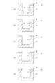
- the hole H formed by etching or the groove H ′ on the side wall side of the bottom surface of the groove H is formed. Is further formed, and an accurate etching shape cannot be obtained.
- the heating temperature of the semiconductor substrate K is gradually increased, as shown in FIG. 2B, the size of the groove H ′ to be formed gradually decreases, and finally, FIG. As shown in c), the groove H ′ is not formed.
- the etching is likely to proceed isotropically, as shown in FIGS. 2 (d) and 2 (e). As shown, the sidewalls of the hole H and the groove H are etched.
- the atoms constituting the semiconductor substrate K do not react with the radicals and ions generated by the plasma formation of the etching gas unless the bond is broken.
- the higher the temperature of the semiconductor substrate K the more Since the bonds are easily broken and radicals and ions generated by making the etching gas into plasma easily react with atoms constituting the semiconductor substrate K, etching by this reaction proceeds efficiently.
- the bond between silicon (Si) and carbon (C) is strong, but the bond between the two increases as the temperature increases. Easy to cut and easy to etch. Therefore, as the heating temperature of the semiconductor substrate K increases, the etching of the wide gap semiconductor substrate K progresses isotropically, and the sidewalls of the holes H and the grooves H are easily etched. 2D and 2E show the etching shape when the heating temperature of the semiconductor substrate K is higher in FIG. 2E. Moreover, in FIG. 2, the code
- the relationship between the heating temperature of the semiconductor substrate and the etching shape was examined. If the heating temperature of the semiconductor substrate was 200 ° C. to 400 ° C., the hole H was removed when plasma etching was performed. The groove H ′ is not formed at all on the bottom surface of the groove H or the groove H ′ is very small even if it is formed, and the side wall of the hole H or the groove H is not etched at all or is etched very little. It was confirmed that it was slight. Therefore, if the semiconductor substrate is heated to 200 ° C. to 400 ° C., the semiconductor substrate can be etched with high accuracy.
- the heating temperature of the semiconductor substrate is more preferably in the range of 300 ° C. to 400 ° C.
- the semiconductor substrate when the semiconductor substrate is plasma-etched, the semiconductor substrate is heated to 200 ° C. to 400 ° C., so that the semiconductor substrate can be etched with high accuracy. .
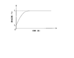
- FIG. 1 By the way, in order to raise the temperature of the semiconductor substrate from the temperature T 0 before heating to the temperature T 1 during the etching process (200 ° C. ⁇ T 1 ⁇ 400 ° C.), as shown in FIG. Take it.
- the temperature of the semiconductor substrate begins to etch the semiconductor substrate by supplying an etching gas into the processing chamber before reaching the etching process temperatures T 1, the temperature of the semiconductor substrate reaches the etching temperature T 1 of the start of etching
- the etching process conditions fluctuate due to the temperature change of the semiconductor substrate, the semiconductor substrate cannot be etched with high accuracy (for example, formed by etching in a time zone in which the temperature of the semiconductor substrate is low, FIGS. 2 (a) and FIG. 2 (b) groove H 'as shown in does not go away even entirely by etching of the semiconductor substrate temperature from when the etching temperature T 1) and a problem that the etching rate Causes the problem of non-uniformity.
- the semiconductor substrate is heated in advance until the temperature reaches the temperature at the time of etching, and then the semiconductor substrate is etched by plasma etching gas while maintaining the temperature of the semiconductor substrate at the temperature at the time of etching.
- an inert gas is supplied into the processing chamber to generate plasma, and a bias potential is applied to the base so that the inertness is achieved.
- the semiconductor substrate may be heated by making ions generated by gas plasma incident on the semiconductor substrate. In this way, the semiconductor substrate can be raised to a predetermined temperature while preventing etching due to ion incidence. Further, the semiconductor substrate can be heated only by generating plasma of an inert gas without newly providing a heating means for heating the semiconductor substrate.
- the semiconductor substrate in order to maintain the temperature of the semiconductor substrate at a constant temperature, it is preferable to heat the semiconductor substrate by the incidence of ions generated by the plasma of the etching gas.
- heating the semiconductor substrate when heating the semiconductor substrate, it may be heated by a heater, or may be heated by both ion incidence and a heater. Further, when the temperature of the semiconductor substrate is excessively increased, cooling of the semiconductor substrate may be combined.
- the semiconductor substrate contains at least one of boron, carbon, nitrogen, and oxygen, such as silicon carbide, gallium nitride, aluminum nitride, zinc oxide, boron nitride, and boron phosphide.
- boron silicon carbide
- gallium nitride aluminum nitride
- zinc oxide boron nitride
- boron phosphide boron phosphide
- the plasma etching method of the present invention it is possible to perform highly accurate plasma etching by setting the heating temperature of the semiconductor substrate to 200 ° C. to 400 ° C.
- the silicon carbide substrate K has, for example, a 4H—SiC crystal structure, and a silicon dioxide film, for example, is formed on the surface as an etching mask. A mask pattern having a predetermined shape is formed.
- the etching apparatus 1 includes a processing chamber 11 having a closed space, a base 15 that is disposed in the processing chamber 11 so as to be movable up and down, and on which the silicon carbide substrate K is placed, Elevating cylinder 18 that raises and lowers table 15, exhaust device 20 that reduces the pressure in processing chamber 11, gas supply device 25 that supplies etching gas and inert gas into processing chamber 11, and supply into processing chamber 11
- a plasma generation device 30 that converts the etching gas and the inert gas into plasma and a high-frequency power source 35 that supplies high-frequency power to the base 15 are provided.
- the processing chamber 11 includes a lower chamber 12 and an upper chamber 13 having internal spaces communicating with each other.
- the upper chamber 13 is formed smaller than the lower chamber 12.
- the base 15 includes an upper member 16 on which the silicon carbide substrate K is placed and a lower member 17 to which the elevating cylinder 18 is connected, and is disposed in the lower chamber 12.
- the exhaust device 20 includes an exhaust pipe 21 connected to a side surface of the lower chamber 12, and exhausts the gas in the processing chamber 11 through the exhaust pipe 21 to bring the inside of the processing chamber 11 to a predetermined pressure.
- the gas supply apparatus 25 as the etching gas, for example, supplied SF 6 gas or an etching gas supply unit 26 for supplying a mixed gas of SF 6 gas and O 2 gas, for example, an inert gas such as He gas
- a mixed gas of SF 6 gas and O 2 gas for example, an inert gas such as He gas
- An inert gas supply unit 27, and a supply pipe 28 having one end connected to the upper surface of the upper chamber 13 and the other end branched and connected to the etching gas supply unit 26 and the inert gas supply unit 27, respectively.
- An etching gas is supplied from the gas supply unit 26 into the processing chamber 11 through the supply pipe 28, and an inert gas is supplied from the inert gas supply unit 27 into the processing chamber 11 through the supply pipe 28.
- the plasma generating apparatus 30 includes a plurality of annular coils 31 that are arranged in the vertical direction on the outer peripheral portion of the upper chamber 13, and a high-frequency power source 32 that supplies high-frequency power to each coil 31.
- a high-frequency power source 32 that supplies high-frequency power to each coil 31.
- the high-frequency power source 35 supplies high-frequency power to the base 15 to generate a potential difference (bias potential) between the base 15 and the plasma, and ions generated by converting the etching gas and the inert gas into plasma. Is incident on the silicon carbide substrate K.
- the silicon carbide substrate K is carried into the etching apparatus 1 and placed on the base 15.
- the temperature of the silicon carbide substrate K is 200 ° C. to 400 ° C. (etching temperature).
- the silicon carbide substrate K is heated until it reaches.
- the inert gas is supplied from the inert gas supply unit 27 into the processing chamber 11, the inside of the processing chamber 11 is brought to a predetermined pressure by the exhaust device 20, and the coil 31 and the high-frequency power sources 32 and 35 are used. High frequency power is respectively supplied to the base 15.
- the inert gas supplied into the processing chamber 11 is converted into plasma, and ions generated by the plasma are incident on and collide with the silicon carbide substrate K by a bias potential. Thereby, silicon carbide substrate K is heated to rise in temperature, and eventually reaches equilibrium at the etching processing temperature.
- whether or not the temperature of the silicon carbide substrate K has reached the etching processing temperature can be determined by, for example, the heating time or temperature measurement of the silicon carbide substrate K.
- the silicon dioxide film as an etching mask has higher heat resistance than the resist, even if the silicon carbide substrate K is heated to 200 ° C. to 400 ° C., it is softened and the shape accuracy of the mask pattern is reduced. Absent.
- the silicon carbide substrate K is etched using the silicon dioxide film as a mask.
- the etching gas is supplied from the etching gas supply unit 26 into the processing chamber 11, the inside of the processing chamber 11 is brought to a predetermined pressure by the exhaust device 20, and the coil 31 and the base are supplied by the high frequency power sources 32 and 35. 15 is supplied with high frequency power.
- the etching gas supplied into the processing chamber 11 is turned into plasma, and the silicon carbide substrate K is etched by radicals and ions generated by the plasma. In the silicon carbide substrate K, holes and grooves corresponding to the mask pattern of the silicon dioxide film are formed.
- silicon carbide substrate K is heated by ions incident and colliding with a bias potential, so that the temperature of silicon carbide substrate K is maintained constant (the etching temperature).
- the silicon carbide substrate K is etched by heating to 200 ° C. to 400 ° C. This is because, as a result of the study by the inventors of the present application, when etching silicon carbide substrate K having a strong bond between atoms, silicon carbide substrate K is heated to a temperature of 200 ° C. to 400 ° C. This is because it has been found preferable.
- the etching when the heating temperature of the silicon carbide substrate K is gradually increased from the heating temperature at which the groove H ′ is no longer formed, the etching easily proceeds isotropically, and FIG. 2 (d) and FIG. 2 (e). As shown in FIG. 5, the etching is performed up to the side wall of the hole H or the groove H. Silicon (Si) and carbon (C) composing the silicon carbide substrate K do not react with radicals and ions generated by plasmatization of the etching gas until the bond between the two is broken. The higher the temperature of the substrate K, the more easily the bond between silicon and carbon is broken, and the radicals and ions generated by the etching gas becoming plasma easily react with silicon and carbon, so that the etching by this reaction proceeds efficiently. . Therefore, as the heating temperature of silicon carbide substrate K increases, etching of silicon carbide substrate K proceeds isotropically, and the sidewalls of holes H and grooves H are more easily etched.
- the heating temperature of the silicon carbide substrate K was 200 ° C. to 400 ° C. (more preferably, 300 ° C. to 400 ° C. )
- the groove H ′ is not formed at all on the bottom surface of the hole H or the groove H, or even if it is formed, it is very small.
- the film was not etched at all or very little if etched. Therefore, if silicon carbide substrate K is heated to 200 ° C. to 400 ° C. (more preferably, 300 ° C. to 400 ° C.), silicon carbide substrate K can be etched with high accuracy.
- the silicon carbide substrate K is plasma-etched, the silicon carbide substrate K is heated to 200 ° C. to 400 ° C. It can be etched.
- the etching process is started after the temperature of the silicon carbide substrate K reaches the etching process temperature.
- the etching process temperature T 1 200 ° C. ⁇ T 1 ⁇ 400 ° C.
- the etching process can be stabilized, the silicon carbide substrate K can be etched with high accuracy, and the etching rate can be prevented from becoming uneven.
- silicon carbide substrate K is heated by causing the ions generated by the plasma conversion of the inert gas to enter and collide with the silicon carbide substrate K, the temperature of the silicon carbide substrate K is increased while preventing etching due to ion incidence. Can be made. Further, without providing a heating mechanism for heating silicon carbide substrate K in processing chamber 11, silicon carbide substrate K can be heated simply by generating plasma of an inert gas.
- the silicon carbide substrate K on which the silicon dioxide film as a mask is formed by applying the plasma etching method of this example is etched, as shown in FIG. 2A and FIG. 'Is not formed, and the side walls are not etched as shown in FIGS. 2 (d) and 2 (e), and the etching is performed with high accuracy as shown in FIG. 2 (c). A shape was obtained.
- the processing conditions for heating the silicon carbide substrate K by converting the inert gas into plasma and setting the temperature of the silicon carbide substrate K to an etching processing temperature of 200 ° C. to 400 ° C. are He gas as an inert gas.
- the supply flow rate is 50 sccm
- the pressure in the processing chamber 11 is 3 Pa
- the high frequency power supplied to the coil 31 is 2.5 kW
- the high frequency power supplied to the base 15 is 700 W
- the temperature of the silicon carbide substrate K is etched.
- the processing conditions for etching this silicon carbide substrate K are as follows: the supply flow rate of SF 6 gas, which is an etching gas, is 50 sccm; the pressure in the processing chamber 11 is 3 Pa; The power was 2.5 kW, and the high frequency power supplied to the base 15 was 700 W.
- the etching temperature of silicon carbide substrate K was about 400 ° C.
- the temperature of the silicon carbide substrate K is raised by making the ions generated by the plasma conversion of the inert gas impinge on and collide with the silicon carbide substrate K.
- K may be heated.
- a heater may be embedded in the base 15 and the silicon carbide substrate K may be heated by this heater, or the silicon carbide substrate K may be heated by both ion incidence and the heater.
- the temperature of silicon carbide substrate K rises to a temperature exceeding 400 ° C. due to heating, the temperature of silicon carbide substrate K is set to a range of 200 ° C. to 400 ° C. by combining cooling of silicon carbide substrate K. It is good to control.
- the silicon carbide substrate having a 4H—SiC crystal structure is taken as an example of the etching target substrate K, but the etching target substrate K may be a silicon carbide substrate having a crystal structure other than 4H—SiC.
- a compound semiconductor substrate such as gallium nitride, aluminum nitride, zinc oxide, boron nitride, and boron phosphide may be used.
- a metal mask such as a nickel film can be employed as the etching mask for the silicon carbide substrate K.
- the etching apparatus 1 is used to perform the plasma etching method according to the present invention.
- the plasma etching method may be performed using an etching apparatus having another structure.
Landscapes
- Engineering & Computer Science (AREA)
- Physics & Mathematics (AREA)
- Condensed Matter Physics & Semiconductors (AREA)
- General Physics & Mathematics (AREA)
- Manufacturing & Machinery (AREA)
- Computer Hardware Design (AREA)
- Microelectronics & Electronic Packaging (AREA)
- Power Engineering (AREA)
- Chemical & Material Sciences (AREA)
- Crystallography & Structural Chemistry (AREA)
- Plasma & Fusion (AREA)
- Drying Of Semiconductors (AREA)
Priority Applications (4)
| Application Number | Priority Date | Filing Date | Title |
|---|---|---|---|
| KR1020117023438A KR101861709B1 (ko) | 2009-10-27 | 2010-09-06 | 플라즈마 식각 방법 |
| US13/318,279 US8673781B2 (en) | 2009-10-27 | 2010-09-06 | Plasma etching method |
| EP10826431.8A EP2495757B1 (en) | 2009-10-27 | 2010-09-06 | Plasma etching method |
| CN2010800266927A CN102473630A (zh) | 2009-10-27 | 2010-09-06 | 等离子蚀刻法 |
Applications Claiming Priority (2)
| Application Number | Priority Date | Filing Date | Title |
|---|---|---|---|
| JP2009246096A JP5179455B2 (ja) | 2009-10-27 | 2009-10-27 | プラズマエッチング方法 |
| JP2009-246096 | 2009-10-27 |
Publications (1)
| Publication Number | Publication Date |
|---|---|
| WO2011052296A1 true WO2011052296A1 (ja) | 2011-05-05 |
Family
ID=43921726
Family Applications (1)
| Application Number | Title | Priority Date | Filing Date |
|---|---|---|---|
| PCT/JP2010/065203 Ceased WO2011052296A1 (ja) | 2009-10-27 | 2010-09-06 | プラズマエッチング方法 |
Country Status (6)
| Country | Link |
|---|---|
| US (1) | US8673781B2 (enExample) |
| EP (1) | EP2495757B1 (enExample) |
| JP (1) | JP5179455B2 (enExample) |
| KR (1) | KR101861709B1 (enExample) |
| CN (1) | CN102473630A (enExample) |
| WO (1) | WO2011052296A1 (enExample) |
Cited By (2)
| Publication number | Priority date | Publication date | Assignee | Title |
|---|---|---|---|---|
| JP2013048160A (ja) * | 2011-08-29 | 2013-03-07 | Panasonic Corp | ドライエッチング方法 |
| EP2755230A4 (en) * | 2011-09-05 | 2015-05-20 | Spp Technologies Co Ltd | plasma etching |
Families Citing this family (7)
| Publication number | Priority date | Publication date | Assignee | Title |
|---|---|---|---|---|
| FR2934709B1 (fr) * | 2008-08-01 | 2010-09-10 | Commissariat Energie Atomique | Structure d'echange thermique et dispositif de refroidissement comportant une telle structure. |
| WO2012008179A1 (ja) * | 2010-07-12 | 2012-01-19 | 住友精密工業株式会社 | エッチング方法 |
| JP5877982B2 (ja) * | 2011-09-22 | 2016-03-08 | Sppテクノロジーズ株式会社 | プラズマエッチング方法 |
| JP5888027B2 (ja) * | 2012-03-14 | 2016-03-16 | 富士通株式会社 | 半導体装置の製造方法 |
| US20140342569A1 (en) * | 2013-05-16 | 2014-11-20 | Applied Materials, Inc. | Near surface etch selectivity enhancement |
| JP5874687B2 (ja) * | 2013-05-31 | 2016-03-02 | 豊田合成株式会社 | 半導体素装置の製造方法 |
| JP2017005177A (ja) * | 2015-06-12 | 2017-01-05 | 株式会社日立ハイテクノロジーズ | プラズマ処理装置およびプラズマ処理方法 |
Citations (4)
| Publication number | Priority date | Publication date | Assignee | Title |
|---|---|---|---|---|
| JPH06169018A (ja) * | 1992-11-30 | 1994-06-14 | Nec Corp | 半導体装置の製造方法 |
| JP2008294210A (ja) | 2007-05-24 | 2008-12-04 | Fuji Electric Device Technology Co Ltd | 炭化珪素半導体装置の製造方法 |
| JP2009064998A (ja) * | 2007-09-07 | 2009-03-26 | Ulvac Japan Ltd | ドライエッチング方法 |
| JP2009194194A (ja) * | 2008-02-15 | 2009-08-27 | Sumitomo Precision Prod Co Ltd | プラズマ処理方法 |
Family Cites Families (14)
| Publication number | Priority date | Publication date | Assignee | Title |
|---|---|---|---|---|
| JPH088232A (ja) * | 1994-06-22 | 1996-01-12 | Sony Corp | プラズマ処理方法 |
| US5571374A (en) * | 1995-10-02 | 1996-11-05 | Motorola | Method of etching silicon carbide |
| JPH10303185A (ja) | 1997-04-26 | 1998-11-13 | Anelva Corp | エッチング装置及びエッチング方法 |
| JPH11162958A (ja) * | 1997-09-16 | 1999-06-18 | Tokyo Electron Ltd | プラズマ処理装置及びその方法 |
| JP2001144075A (ja) | 1999-11-15 | 2001-05-25 | Matsushita Electric Ind Co Ltd | プラズマ処理装置 |
| US6475889B1 (en) * | 2000-04-11 | 2002-11-05 | Cree, Inc. | Method of forming vias in silicon carbide and resulting devices and circuits |
| US6670278B2 (en) * | 2001-03-30 | 2003-12-30 | Lam Research Corporation | Method of plasma etching of silicon carbide |
| JP2003069154A (ja) * | 2001-06-11 | 2003-03-07 | Sharp Corp | 半導体レーザ素子およびその製造方法 |
| JP2003273084A (ja) * | 2002-03-15 | 2003-09-26 | Seiko Epson Corp | 大気圧プラズマ装置、大気圧プラズマ処理方法及びデバイス並びにデバイス製造方法 |
| JP4030982B2 (ja) | 2004-05-10 | 2008-01-09 | ユーディナデバイス株式会社 | 半導体装置および半導体装置の製造方法 |
| US7465670B2 (en) * | 2005-03-28 | 2008-12-16 | Tokyo Electron Limited | Plasma etching method, plasma etching apparatus, control program and computer storage medium with enhanced selectivity |
| JP4859474B2 (ja) * | 2006-02-15 | 2012-01-25 | 三菱重工業株式会社 | プラズマ処理方法、及び、プラズマ処理装置 |
| JP4516538B2 (ja) | 2006-03-01 | 2010-08-04 | 住友電工デバイス・イノベーション株式会社 | 半導体装置の製造方法 |
| JP5309587B2 (ja) | 2008-02-07 | 2013-10-09 | 富士電機株式会社 | 炭化珪素半導体基板のトレンチエッチング方法 |
-
2009
- 2009-10-27 JP JP2009246096A patent/JP5179455B2/ja active Active
-
2010
- 2010-09-06 US US13/318,279 patent/US8673781B2/en active Active
- 2010-09-06 EP EP10826431.8A patent/EP2495757B1/en active Active
- 2010-09-06 WO PCT/JP2010/065203 patent/WO2011052296A1/ja not_active Ceased
- 2010-09-06 CN CN2010800266927A patent/CN102473630A/zh active Pending
- 2010-09-06 KR KR1020117023438A patent/KR101861709B1/ko active Active
Patent Citations (4)
| Publication number | Priority date | Publication date | Assignee | Title |
|---|---|---|---|---|
| JPH06169018A (ja) * | 1992-11-30 | 1994-06-14 | Nec Corp | 半導体装置の製造方法 |
| JP2008294210A (ja) | 2007-05-24 | 2008-12-04 | Fuji Electric Device Technology Co Ltd | 炭化珪素半導体装置の製造方法 |
| JP2009064998A (ja) * | 2007-09-07 | 2009-03-26 | Ulvac Japan Ltd | ドライエッチング方法 |
| JP2009194194A (ja) * | 2008-02-15 | 2009-08-27 | Sumitomo Precision Prod Co Ltd | プラズマ処理方法 |
Non-Patent Citations (2)
| Title |
|---|
| J.R.FLEMISH ET AL.: "Smooth etching of single crystal 6H-SiC in an electron cyclotron resonance plasma reactor", APPLIED PHYSICS LETTERS, vol. 64, no. 17, 25 April 1994 (1994-04-25), pages 2315 - 2317, XP002021930 * |
| See also references of EP2495757A4 |
Cited By (2)
| Publication number | Priority date | Publication date | Assignee | Title |
|---|---|---|---|---|
| JP2013048160A (ja) * | 2011-08-29 | 2013-03-07 | Panasonic Corp | ドライエッチング方法 |
| EP2755230A4 (en) * | 2011-09-05 | 2015-05-20 | Spp Technologies Co Ltd | plasma etching |
Also Published As
| Publication number | Publication date |
|---|---|
| KR101861709B1 (ko) | 2018-05-28 |
| JP5179455B2 (ja) | 2013-04-10 |
| US8673781B2 (en) | 2014-03-18 |
| JP2011096700A (ja) | 2011-05-12 |
| EP2495757A4 (en) | 2013-02-20 |
| US20120052688A1 (en) | 2012-03-01 |
| KR20120073160A (ko) | 2012-07-04 |
| EP2495757A1 (en) | 2012-09-05 |
| EP2495757B1 (en) | 2020-04-22 |
| CN102473630A (zh) | 2012-05-23 |
Similar Documents
| Publication | Publication Date | Title |
|---|---|---|
| JP5179455B2 (ja) | プラズマエッチング方法 | |
| JP5762491B2 (ja) | エッチング方法 | |
| US9443701B2 (en) | Etching method | |
| KR101020334B1 (ko) | 마이크로파 플라즈마 처리 장치 | |
| KR102797626B1 (ko) | 원자 층 제어를 사용한 막의 등방성 에칭 | |
| CN104616984B (zh) | 等离子蚀刻处理方法以及等离子蚀刻处理装置 | |
| WO2013042497A1 (ja) | プラズマエッチング方法 | |
| JP6567487B2 (ja) | プラズマエッチング方法 | |
| JP6130313B2 (ja) | プラズマエッチング方法 | |
| JP2012054616A (ja) | プラズマエッチング方法 | |
| JP2012054616A5 (enExample) | ||
| JP2016051777A (ja) | シリコン酸化膜のプラズマエッチング方法 | |
| JP2025529475A (ja) | 選択的等方性エッチングを実現するための表面改質 | |
| CN108091559B (zh) | 一种蓝宝石衬底的刻蚀方法 | |
| JP6295130B2 (ja) | ドライエッチング方法 | |
| WO2019017367A1 (ja) | 切断加工方法 | |
| JP7277225B2 (ja) | エッチング方法、及び、プラズマ処理装置 | |
| KR102851427B1 (ko) | 기판 처리 방법 | |
| JP2009038262A (ja) | プラズマ処理装置 |
Legal Events
| Date | Code | Title | Description |
|---|---|---|---|
| WWE | Wipo information: entry into national phase |
Ref document number: 201080026692.7 Country of ref document: CN |
|
| 121 | Ep: the epo has been informed by wipo that ep was designated in this application |
Ref document number: 10826431 Country of ref document: EP Kind code of ref document: A1 |
|
| ENP | Entry into the national phase |
Ref document number: 20117023438 Country of ref document: KR Kind code of ref document: A |
|
| WWE | Wipo information: entry into national phase |
Ref document number: 13318279 Country of ref document: US |
|
| WWE | Wipo information: entry into national phase |
Ref document number: 2010826431 Country of ref document: EP |
|
| NENP | Non-entry into the national phase |
Ref country code: DE |