WO2011027768A1 - Ad変換器および固体撮像装置 - Google Patents
Ad変換器および固体撮像装置 Download PDFInfo
- Publication number
- WO2011027768A1 WO2011027768A1 PCT/JP2010/064891 JP2010064891W WO2011027768A1 WO 2011027768 A1 WO2011027768 A1 WO 2011027768A1 JP 2010064891 W JP2010064891 W JP 2010064891W WO 2011027768 A1 WO2011027768 A1 WO 2011027768A1
- Authority
- WO
- WIPO (PCT)
- Prior art keywords
- unit
- latch unit
- delay
- signal
- data
- Prior art date
Links
- 238000003384 imaging method Methods 0.000 title claims description 68
- 238000006243 chemical reaction Methods 0.000 claims abstract description 36
- 230000007704 transition Effects 0.000 claims abstract description 23
- 230000007423 decrease Effects 0.000 claims abstract description 6
- 238000000034 method Methods 0.000 claims description 42
- 230000008569 process Effects 0.000 claims description 35
- 238000004364 calculation method Methods 0.000 claims description 11
- 230000003111 delayed effect Effects 0.000 claims description 10
- 230000010354 integration Effects 0.000 claims description 9
- 230000007274 generation of a signal involved in cell-cell signaling Effects 0.000 claims description 7
- 238000013139 quantization Methods 0.000 claims description 7
- 230000001934 delay Effects 0.000 claims description 3
- 239000011159 matrix material Substances 0.000 claims description 3
- 238000012545 processing Methods 0.000 abstract description 27
- 238000010586 diagram Methods 0.000 description 44
- 230000008859 change Effects 0.000 description 10
- 239000000872 buffer Substances 0.000 description 7
- 230000010355 oscillation Effects 0.000 description 7
- 230000000630 rising effect Effects 0.000 description 7
- 230000010363 phase shift Effects 0.000 description 5
- 230000004044 response Effects 0.000 description 5
- 230000006870 function Effects 0.000 description 4
- 239000004065 semiconductor Substances 0.000 description 4
- 238000001514 detection method Methods 0.000 description 3
- 230000002093 peripheral effect Effects 0.000 description 3
- 230000003321 amplification Effects 0.000 description 2
- 239000003990 capacitor Substances 0.000 description 2
- 230000003247 decreasing effect Effects 0.000 description 2
- 230000001419 dependent effect Effects 0.000 description 2
- 238000004519 manufacturing process Methods 0.000 description 2
- 238000003199 nucleic acid amplification method Methods 0.000 description 2
- 230000000717 retained effect Effects 0.000 description 2
- 230000001360 synchronised effect Effects 0.000 description 2
- 230000003139 buffering effect Effects 0.000 description 1
- 239000002131 composite material Substances 0.000 description 1
- 238000012937 correction Methods 0.000 description 1
- 238000013461 design Methods 0.000 description 1
- 230000014759 maintenance of location Effects 0.000 description 1
- 229910021421 monocrystalline silicon Inorganic materials 0.000 description 1
- 230000003287 optical effect Effects 0.000 description 1
- 238000012546 transfer Methods 0.000 description 1
Images


Classifications
-
- H—ELECTRICITY
- H03—ELECTRONIC CIRCUITRY
- H03M—CODING; DECODING; CODE CONVERSION IN GENERAL
- H03M1/00—Analogue/digital conversion; Digital/analogue conversion
- H03M1/12—Analogue/digital converters
- H03M1/14—Conversion in steps with each step involving the same or a different conversion means and delivering more than one bit
-
- H—ELECTRICITY
- H04—ELECTRIC COMMUNICATION TECHNIQUE
- H04N—PICTORIAL COMMUNICATION, e.g. TELEVISION
- H04N25/00—Circuitry of solid-state image sensors [SSIS]; Control thereof
- H04N25/70—SSIS architectures; Circuits associated therewith
- H04N25/71—Charge-coupled device [CCD] sensors; Charge-transfer registers specially adapted for CCD sensors
- H04N25/75—Circuitry for providing, modifying or processing image signals from the pixel array
-
- H—ELECTRICITY
- H04—ELECTRIC COMMUNICATION TECHNIQUE
- H04N—PICTORIAL COMMUNICATION, e.g. TELEVISION
- H04N25/00—Circuitry of solid-state image sensors [SSIS]; Control thereof
- H04N25/70—SSIS architectures; Circuits associated therewith
- H04N25/76—Addressed sensors, e.g. MOS or CMOS sensors
- H04N25/78—Readout circuits for addressed sensors, e.g. output amplifiers or A/D converters
-
- H—ELECTRICITY
- H03—ELECTRONIC CIRCUITRY
- H03M—CODING; DECODING; CODE CONVERSION IN GENERAL
- H03M1/00—Analogue/digital conversion; Digital/analogue conversion
- H03M1/12—Analogue/digital converters
- H03M1/50—Analogue/digital converters with intermediate conversion to time interval
- H03M1/56—Input signal compared with linear ramp
Definitions
- the present invention relates to an AD converter (analog-digital converter) and a solid-state imaging device using the AD converter.
- AD converter analog-digital converter
- This application claims priority based on Japanese Patent Application No. 2009-201522 for which it applied to Japan on September 1, 2009, and uses the content here.
- Patent Documents 1 to 4 As an example using an AD converter according to a conventional example, configurations described in Patent Documents 1 to 4 are known. First, the configuration and operation of the AD converter disclosed in Patent Document 1 will be described.
- FIG. 24 is a configuration diagram of a MOS sensor using an AD converter according to a first conventional example described in Patent Document 1.
- This MOS sensor includes an AD conversion circuit 1106 that includes a comparator 1107 and a digital memory 1108 for each column of pixels 1101.
- a digital (binary) value output from the counter 1104 is input to a DA conversion circuit (hereinafter referred to as DAC) 1105.
- the DAC 1105 generates a ramp voltage (ramp wave) 1122 corresponding to the input digital value, and outputs the ramp voltage (ramp wave) 1122 to one of the input units of the comparator 1107 as a reference signal.
- the output of the counter 1104 is distributed to the digital memory 1108 of each column via the binary ⁇ Gray code converter 1115.
- a pixel signal is input from the pixel 1101 to the other input portion of the comparator 1107 in each AD conversion circuit 1106 via the readout signal line 1103 as an analog signal to be subjected to AD conversion.
- the AD conversion operation according to the first conventional example will be described.
- the counter 1104 starts counting from its initial value, and at the same time, the DAC 1105 starts generating the ramp voltage (ramp wave) 1122.
- a readout signal from the pixel 1101 in each column and a common ramp voltage (ramp wave) 1122 that changes in synchronization with the count value of the counter 1104 are input to the comparator 1107 in each column.
- the count value of the counter 1104 is distributed to the digital memory 1108.
- the AD conversion method described above is a method called ramp-type AD conversion (Ramp Run-up ADC), and according to the general classification of AD conversion, a method called counting ADC (counting AD conversion). It is.
- Using a ramp voltage (ramp wave) as a reference signal is equivalent to converting an analog signal potential from a pixel into a length of time, and measuring the length of time using a fixed frequency clock signal. This name is used to realize AD conversion.
- the count value of the counter 1104 is set to the upper bits, and the phase of the clock (or the clock output from the counter) input to the counter is set.
- a multiphase clock is generated by delaying, and the logic state is set to a lower bit, thereby further improving the resolution.
- the number of pixels is 20 million pixels and the frame rate is 60 frame / sec.
- This calculation does not take into account the waiting period until the AD converter circuit receives data from the pixel or the period during which the AD conversion result is transferred to the output memory, that is, the period during which comparison operation cannot be performed as AD conversion.
- the same calculation is performed using the AD converter according to the second conventional example.
- the upper bits need only change the count value of the counter output to the digital memory at about 60 MHz, which is 256 times the read rate of one row.
- the phase of the clock input to the counter (or the clock output from the counter) is delayed by 0, ⁇ / 4, ⁇ / 2, 3 ⁇ / 4, and the logic state is held and encoded Get digital value.
- the 10 bits consist of the upper 6 bits and the lower 4 bits
- the upper bits only change the count value of the counter output to the digital memory at about 15 MHz, which is 64 times the read rate of one row. Just do it.
- the phase of the clock input to the counter (or the clock output from the counter) is 0, ⁇ / 16, ⁇ / 8, 3 ⁇ / 16, ⁇ / 4, 5 ⁇ / 16, 3 ⁇ / 8, 7 ⁇ / Digital value by delaying 16, ⁇ / 2, 9 ⁇ / 16, 5 ⁇ / 8, 11 ⁇ / 16, 3 ⁇ / 4, 13 ⁇ / 16, 7 ⁇ / 8, 15 ⁇ / 16, retaining and encoding its logic state To get.
- the conventional AD converter has a problem regarding the accuracy of AD conversion as described below. (1) The upper bit and the lower bit are not completely dependent operations. (2) It is difficult to binarize the retained data of the lower bits accurately.
- the binarization of the lower bits is performed based on the logic state of the multiphase clock held in the digital memory. Especially when acquiring the logic state at the latch timing in high-speed operation, [1] the logic state changes from the high state to the low state, or [2] the logic state changes from the low state to the high state. High state in the middle is mixed (probability increases). This makes binarization difficult.
- the first reason why binarization is difficult is that the rise time and fall time of the circuit are not necessarily equal.
- CMOS circuit for example, a CMOS inverter circuit
- the setting of the threshold voltage of the PMOS transistor and the setting of the threshold voltage of the NMOS transistor are performed in different steps.
- the rise time of the output voltage of the circuit is mainly determined by the threshold voltage of the PMOS transistor, and the fall time of the circuit is mainly determined by the threshold voltage of the NMOS transistor. Therefore, the rise time and fall time of the output voltage of the circuit are not special phenomena but a general phenomenon that occurs from the manufacturing process.
- the second reason why binarization is difficult is that even if the rise time and the fall time can be made equal, the threshold value of the holding circuit (latch circuit) actually depends on the power supply voltage fluctuation or temperature change. This is because the voltage fluctuates, and as a result, an erroneous logic state may be held. In order to avoid this problem, it is necessary to incorporate a means for detecting power supply voltage fluctuations and temperature changes to control the circuit. However, the circuit scale is increased and power consumption is increased accordingly.
- the present invention has been made in view of the above-described problems, and an object thereof is to provide an AD converter that can perform AD conversion with higher accuracy and a solid-state imaging device using the AD converter.
- An AD converter includes a reference signal generation unit that generates a reference signal that increases or decreases over time, and compares the analog signal with the reference signal at a timing related to input of the analog signal to be subjected to AD conversion.
- a comparator that finishes the comparison process at a timing when the reference signal satisfies a predetermined condition with respect to the analog signal, and a plurality of delay units having the same configuration.
- An annular delay circuit that starts a transition operation at such timing, a count unit that counts clocks from the annular delay circuit, and logical states of the plurality of delay units at a first timing related to the end of the comparison process
- a lower latch unit that latches the lower logical state, and a higher level that is the logical state of the count unit at the first timing related to the end of the comparison process
- An upper latch unit that latches a logic state; and an arithmetic unit that calculates a digital signal corresponding to the analog signal based on data of the lower latch unit and the upper latch unit.
- the number of the plurality of delay units is an odd number.
- the number of the plurality of delay units is an odd number, and each of the plurality of delay units further includes an odd number of inverting elements.
- the odd number of the inverting elements constituting the delay unit is configured by a fully differential inverting circuit.
- the plurality of delay units are configured to be able to control the delay amount.
- the delay amounts of the plurality of delay units are controlled by a current flowing through the delay units.
- the arithmetic unit sequentially rises the data of the lower latch unit, which is an output from the plurality of delay units, at a certain time interval, or sequentially at a certain time interval. It is desirable that the operation unit detect the transition position of the state in the signal group at the first timing related to the end of the comparison process.
- the count unit outputs a redundant upper logical state in addition to the upper logical state, and the redundant upper logical state as a latch unit other than the lower latch unit and the upper latch unit.
- a redundant upper latch state for latching wherein the redundant upper logical state is a delay of at least part of the upper logical state by a certain time, or the upper logical state is at least part of the redundant upper logical state Is preferably delayed by a certain amount of time.
- the comparison unit may include a signal indicating the first timing related to the end of the comparison process and a second timing obtained by delaying the first timing by a certain delay time. It is desirable to output a signal indicating the above.
- the reference signal generation unit is configured using an integration circuit.
- the reference signal generation unit is configured using a DAC circuit.
- the reference signal generation unit further includes an LPF circuit after the DAC circuit.
- the filter constant of the LPF circuit is controlled according to at least the delay amount of the delay unit and the quantization step of the DAC circuit.
- the present invention is an AD conversion target for an imaging unit in which a plurality of pixels that output pixel signals according to the magnitude of incident electromagnetic waves are arranged in a matrix and an analog signal corresponding to the pixel signals. It is a solid-state imaging device having the AD converter that is an analog signal, and a control unit that controls the imaging unit and the AD converter.
- the pixel signal includes a reference level and a signal level
- the comparison unit compares the reference level with the reference signal
- the upper latch unit includes a first upper latch unit and a second upper latch unit
- the lower latch unit includes A first lower latch unit and a second lower latch unit, and holding the first data related to the first comparison process and the second data related to the second comparison process.
- the first data is held in the first upper latch unit and the first lower latch unit, and the held first data is stored in the second upper latch unit. It is preferable that the second data is held in the first upper latch unit and the first lower latch unit after being transferred to the second lower latch unit.
- the count unit further outputs the redundant upper logical state in addition to the upper logical state
- the upper latch unit includes the first upper latch unit and the second upper latch unit.
- the first redundant upper latch unit and the second redundant upper latch unit are further included, and the lower latch unit includes a first lower latch unit and a second lower latch unit. It is desirable.
- the first data is held in the first upper latch unit, the first redundant upper latch unit, and the first lower latch unit, and the held data is stored in the first upper latch unit, the first redundant upper latch unit, and the first lower latch unit.
- the second data is transferred to the first upper latch unit and the first redundant upper unit. It is desirable to hold in the latch unit and the first lower latch unit.
- the data holding in the first or second upper latch unit is the first timing related to the end of the comparison process or the first timing related to the end of the comparison process. 1 is performed at one of the second timings delayed by a delay time, and the data retention of the first or second redundant upper latch unit is performed at the first timing related to the end of the comparison process. Alternatively, it is preferable that the first timing related to the end of the comparison process is performed at the other of the second timings delayed by a certain delay time.
- the counting unit is provided for each column or a plurality of columns of the imaging unit as a column counting unit, and a clock from the annular delay circuit is used as a count clock of the column counting unit. It is desirable to use as.
- the column count unit has an up-count mode and a down-count mode, and performs the count related to the first comparison processing by either down-counting or up-counting, and the second counting It is preferable that the count related to the comparison process is performed by the other of the down-count and the up-count.
- the upper logical state and the lower logical state are based on the output of the same annular delay circuit, so AD conversion is performed with higher accuracy. be able to.
- the first latch timing is related to the end of the comparison process by rearranging the data in the lower latch section into a signal group that sequentially rises at a constant time interval or rearranges at a constant time interval.
- FIG. 1 It is a block diagram which shows the structure of the AD converter by the 1st Embodiment of this invention. It is a block diagram which shows the structure of VCO which the AD converter by the 1st Embodiment of this invention has. It is a block diagram which shows the partial structure of VCO which the AD converter by the 1st Embodiment of this invention has. It is a block diagram which shows the partial structure of VCO which the AD converter by the 1st Embodiment of this invention has. It is a block diagram which shows the partial structure of VCO which the AD converter by the 1st Embodiment of this invention has. It is a block diagram which shows the partial structure of VCO which the AD converter by the 1st Embodiment of this invention has. It is a block diagram which shows the partial structure of VCO which the AD converter by the 1st Embodiment of this invention has. FIG.
- FIG. 3 is a configuration diagram and timing chart for explaining an operation of detecting a lower logical state of a VCO included in the AD converter according to the first embodiment of the present invention.
- FIG. 3 is a configuration diagram and timing chart for explaining an operation of detecting a lower logical state of a VCO included in the AD converter according to the first embodiment of the present invention.
- It is a block diagram which shows the structure of the lamp
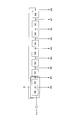
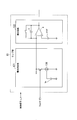
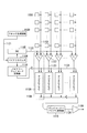
- FIG. 1 is an example of a configuration diagram of an entire AD converter according to the first embodiment of the present invention.
- the configuration shown in FIG. 1 will be described below.
- the AD converter includes a ramp unit 19, a comparison unit 108, a VCO 101, a count unit 103, a lower latch unit 105, an upper latch unit 107, and a calculation unit 117.
- the ramp unit 19 generates a reference signal (ramp wave) that increases or decreases over time.
- the comparison unit 108 outputs a comparison result between the first input terminal IN1 to which the analog signal Vin to be AD converted is input, the second input terminal IN2 to which the ramp wave from the ramp unit 19 is input, and the comparison result. And a third terminal OUT.
- the VCO 101 is an annular delay circuit having n delay units (Delay ⁇ Unit) (n is a natural number of 2 or more).
- the counting unit 103 counts clocks from the VCO 101.
- the lower latch unit 105 holds the lower logic state of the VCO 101.
- the upper latch unit 107 holds the upper logic state of the count unit 103.
- the arithmetic unit 117 calculates a digital signal based on the data of the lower latch unit 105 and the upper latch unit 107.
- the VCO 101 starts a transition operation and the count unit 103 starts counting from its initial value.
- the ramp unit 19 starts generating a ramp wave.
- the analog signal Vin subject to AD conversion and the ramp wave that changes (increases or decreases) substantially in synchronization with the upper logic state of the count unit 103 are input to the comparison unit 108, and the comparison unit 108 performs the comparison operation.
- the lower logical state of the VCO 101 is distributed to the lower latch unit 105, and the upper logical state of the count unit 103 is distributed to the upper latch unit 107.
- the output of the comparison unit 108 is inverted, and the lower latch unit 105 and the upper latch unit 107 each hold the input logic state. Since the ramp wave input to the comparison unit 108 and the logic state input to the lower latch unit 105 and the upper latch unit 107 are substantially synchronized, the analog signal to be subjected to AD conversion is converted into the lower latch unit 105 and the upper latch. AD conversion to the value held in the unit 107 is performed. Thereafter, the arithmetic unit 117 calculates composite data from the data of the lower latch unit 105 and the upper latch unit 107.
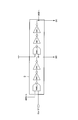
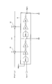
- FIG. 2 is an example of a configuration diagram of the VCO 101 of FIG.
- the VCO 101 has a configuration in which delay units (Delay Unit) are connected in an odd number (9 stages in this example) in an annular shape.
- the delay units DU0 to DU8 output the statuses CK0 to CK8 of the operating delay units from their output terminals.
- the state CK8 is a clock to the count unit 103.
- the number of delay units is nine, but the present invention is not limited to this.
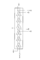
- FIG. 3 is a first example showing an enlarged view of the part D of the delay unit of FIG.
- Each delay unit DU0 to DU8 includes three inverting elements (NAND * _1 and INV * _1 to INV * _2).
- “*” is a number (0 to 8) corresponding to each delay unit DU0 to DU8.
- the number of inversion elements is three.
- the present invention is not limited to this.
- the delay unit is configured using a NAND circuit and an INV (inverter) circuit, other delay units may be used.
- FIG. 4 is a second example showing an enlarged view of the part D of the delay unit of FIG.
- Each delay unit DU0 to DU8 includes three fully differential inverting elements (DE * _1 to DE * _3).
- “*” is a number (0 to 8) corresponding to each delay unit DU0 to DU8.
- the number of fully differential inverting elements is three, but it is not necessary to be limited to this.
- FIG. 5 is a third example showing an enlarged view of the part D of the delay unit in FIG.
- the current sources I1 and I2 for controlling the delay amount of the delay units DU0 to DU8 are inserted in the power supply lines of the inverting elements INV * _1 constituting the delay units DU0 to DU8.
- the delay amount can be varied, and a feedback operation such as operating the VCO 101 in synchronization with another clock, for example, is possible.
- the current source is inserted into the power supply line of the inverting element INV * _1.
- the present invention is not limited to this.
- FIG. 6 is a fourth example showing an enlarged view of part D of the delay unit in FIG.
- the current sources I1 and I2 for controlling the delay amount of the delay units DU0 to DU8 are inserted into the power supply lines of the fully differential inverting elements DE * _2 constituting the delay units DU0 to DU8. It is that. As a result, the delay amount can be varied, and a feedback operation such as operating the VCO 101 in synchronization with another clock, for example, is possible.
- the current source is inserted into the power line of the fully differential inverting element DE * _2.
- the present invention is not limited to this.
- the lower logical state of the delay units DU0 to DU8 constituting the VCO 101 is held in the lower latch unit 105, and the upper logical state of the count unit 103 to which the logical state of the delay unit DU8 is input is stored in the upper latch unit 107. Retained. As a result, the upper logical state and the lower logical state change in synchronization with the same start pulse (StartP), and the phase relationship between the upper logical state and the lower logical state is maintained. ) Can be solved.
- the annular delay circuit itself has an odd number of delay units.
- a so-called asymmetric oscillation circuit whose output is equivalently even (especially a power of 2) may be used.
- the annular delay circuit itself as shown in FIG. 15 is composed of an even number (especially a power of 2) delay units, and the output (terminal) of the lower logic state is an even number (especially a power of 2).
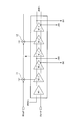
- FIG. 7 is a diagram for explaining the operation of detecting the lower logical state, and is composed of a configuration diagram ((a)) and a timing chart ((b)).
- the VCO 101 has a configuration in which nine delay units are connected.
- the delay units DU0 to DU8 output the statuses CK0 to CK8 of the operating delay units from their output terminals.
- Each delay unit DU0 to DU8 is configured by a NAND circuit (NAND0 to NAND8), and one terminal of the NAND circuit (NAND1 to NAND8) is connected to the power supply VDD.
- the transition operation of the VCO 101 is started, and the signals CK0 to CK8 are repeatedly inverted at a constant time interval. That is, the state of the delay unit in the VCO 101 changes (transitions) sequentially.
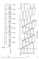
- CK1, CK3, CK5, CK7, CK0, CK2, CK4, CK6, CK8 are rearranged.
- the signal groups rise in order at regular time intervals (or fall in order at regular time intervals).
- the transition position is a location where the state changes from Low to High (or from High to Low) in the rearranged signal group.
- the VCO 101 status output Ts seconds after the logic state of the start pulse (StartP) changes from low to high is low (CK1), low (CK3), low (CK5 ), Low (CK7), High (CK0), High (CK2), High (CK4), High (CK6), and High (CK8), and CK0 is the transition position.
- the transition position where the state has changed from Low to High (or from High to Low moves sequentially with time.
- the transition position detection circuit for example, a technique substantially similar to that of a flash ADC can be employed.
- the transition position can be detected by setting a position where the state has changed from Low to High (or from High to Low) in the rearranged signal group as the transition position. Since this transition position can be detected based on only one of the rising edge and the falling edge of the signal, the problem (2) described above can be solved.
- the lower bit data obtained is not a power of 2.
- the combined data of the upper bits and the lower bits is a power of 2
- simple operations such as addition / subtraction and bit shift are performed. It is possible to easily convert the data to a power of 2 by simple arithmetic processing. Note that this is not necessary if the output described above is equivalent to a power of 2, such as an asymmetric oscillation circuit.
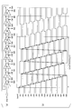
- FIG. 8 is a diagram for explaining the operation of detecting the lower logical state, and is composed of a configuration diagram ((a)) and a timing chart ((b)).
- the VCO 101 has a configuration in which nine delay units (Delay Units) are connected.
- the delay units DU0 to DU8 output the statuses CK0 to CK8 and / CK0 to / CK8 of the operating delay units from the respective output terminals.
- Each delay unit DU0 to DU8 is composed of fully differential inverting elements (DE0 to DE8).
- the VCO 101 starts oscillating, and the signals CK0 to CK8 and / CK0 to / CK8 repeat the inversion operation at regular time intervals. That is, the state of the delay unit in the VCO 101 changes (transitions) sequentially.
- the transition position in the data held at the first timing related to the end of the comparison process is detected.
- the transition position can be detected by using a method almost the same as that of the flash ADC.
- the lower bit data obtained is not a power of 2
- details are omitted, but addition / subtraction, bit shift, etc. It can be easily converted into power-of-two data by simple arithmetic processing. Note that this is not necessary if it is a fully differential oscillation circuit or the like composed of the power-of-two delay units described above.
- the delay unit is composed of a NAND circuit, and when attention is paid to the output of one delay unit, one of High and Low is obtained as a logical state.
- the delay unit is configured by a fully differential inverting element. When attention is paid to the output of one delay unit, both High and Low are obtained as logic states. Due to this difference, in FIG. 7B and FIG. 8B, as shown by the inclination of the arrow, when only the change in the rising position of the signal is followed, FIG. The rising position moves faster than b). That is, in the configuration of FIG. 8A, the change in the transition position in the lower logical state is faster than in the configuration of FIG. 7A, and high-speed operation is possible.
- FIG. 9 is a first example showing a configuration diagram of the lamp unit 19.
- the lamp unit 19 includes a charge supply circuit 121 and an integration circuit 122.
- the charge supply circuit 121 is configured to generate a certain charge every certain time.
- the charge supply circuit 121 includes a variable current source 126 having one end connected to the ground GND and the other end connected to the input of the integrating circuit 122.
- the variable current source 126 is configured such that its current value is variable. Therefore, it is possible to obtain a desired slope as the slope of the ramp wave output from the integrating circuit 122 by changing the current value of the variable current source 126.
- the integration circuit 122 is configured to accumulate the charge generated from the charge supply circuit 121 and convert it into a voltage.
- the integration circuit 122 includes a capacitor C, a voltage source Vref, and an operational amplifier G.
- the voltage source Vref has one end connected to the ground GND and the other end connected to the positive (+) side input terminal of the operational amplifier G. Further, the initial value (starting voltage) of the ramp wave can be set to a desired value by configuring the voltage source Vref as a variable voltage source.
- FIG. 10 is a second example showing a configuration diagram of the lamp unit 19. The difference from FIG. 9 is that one end of the variable current source 126 of the charge supply circuit 121 is connected to the reference power source.
- FIG. 11 is a third example showing a configuration diagram of the lamp unit 19.
- the variable current source is composed of a plurality of NMOS transistors. By varying the voltage of the voltage source Vn applied to the gate electrode of the NMOS transistor and the number of transistors, a ramp wave having a desired slope can be obtained.
- FIG. 12 is a fourth example showing a configuration diagram of the lamp unit 19.
- the variable current source is composed of a plurality of PMOS transistors.
- Vp the voltage of the voltage source
- NMOS transistor the number of transistors
- FIG. 13 is a fifth example showing a configuration diagram of the lamp unit 19.
- the DAC circuit 131 generates a stepped ramp wave in response to an increase in the count value of the count unit 103.
- the LPF circuit 132 is a so-called low frequency pass filter circuit composed of, for example, a resistor and a capacitor.
- the filter circuit need not be limited to this configuration.
- the buffer circuit 133 buffers the ramp wave that has passed through the LPF circuit 132 and outputs it.
- the buffer circuit 133 may be constituted by, for example, a source follower circuit, a voltage follower circuit, or an amplifier capable of voltage amplification.
- FIG. 14 is a diagram schematically showing a state in which the filter constant of the LPF circuit 132 in FIG. 13 is changed.
- the horizontal axis represents time and the vertical axis represents voltage, and the ramp waveform changes by controlling the filter constant.
- the time on the horizontal axis in FIG. 14 is equivalent to the delay amount (time) of the delay unit, and the voltage on the vertical axis is equivalent to the quantization step of the DAC circuit 131.
- control is performed such that the bandwidth is increased when the delay amount is decreased, and the bandwidth is decreased when the delay amount is increased.
- control is performed to reduce the band when the quantization step is small and to increase the band when the quantization step is large. In this way, a smooth ramp wave can be obtained by providing a filter and further controlling the filter constant.
- the delay amount of the delay unit controllable
- feedback control such as synchronizing the VCO 101 with another clock becomes possible.
- feedback control can be performed with an easy configuration.
- the reference signal (ramp wave) is an analog signal by configuring the ramp unit 19 using an integration circuit, high-resolution and high-precision AD conversion can be realized.
- the ramp unit 19 using a DAC circuit the reference signal becomes a digital signal, and thus noise resistance can be improved.
- a digital reference signal can be used as an analog reference signal.
- the digital reference signal is optimized to an analog reference signal according to the driving state, and more It is possible to obtain a reference signal that changes smoothly.
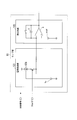
- FIG. 16 is an example of a configuration diagram of the entire AD converter according to the second embodiment of the present invention.
- the difference from FIG. 1 is that a count delay unit 104 and a redundant upper latch unit 106 for delaying the output of the upper logic state from the count unit 103 are provided.
- the count delay unit 104 is controlled by a control signal.
- the upper logical state output from the count unit 103 is delayed by the count delay unit 104 and held by the redundant upper latch unit 106.
- FIG. 1 The difference from FIG. 1 is that a count delay unit 104 and a redundant upper latch unit 106 for delaying the output of the upper logic state from the count unit 103 are provided.
- the count delay unit 104 is controlled by a control signal.
- the upper logical state output from the count unit 103 is delayed by the count delay unit 104 and held by the redundant upper latch unit 106.
- the upper logical state and the redundant upper logical state obtained by delaying the upper logical state can be output, for example, a deviation (mismatch) occurs in the timing of holding data between the lower logical state and the upper logical state. Even in this case, it is possible to correct the data by using the data holding the redundant upper logical state.
- the upper logical state is delayed as the redundant upper logical state, but the redundant upper logical state may be delayed as the upper logical state.
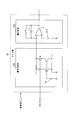
- FIG. 17 is a second example of a configuration diagram of the entire AD converter according to the present embodiment.
- the difference from FIG. 1 is that a comparison delay unit 109 for delaying the comparison result in the comparison unit 108 is provided.
- the comparison delay unit 109 is controlled by a control signal.
- One of the signal output from the comparison unit 108 and the signal output from the comparison delay unit 109 controls the latch timing of the lower latch unit 105, and the other controls the latch timing of the upper latch unit 107.
- it is the same as in FIG.
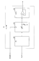
- FIG. 18 is a third example of a configuration diagram of the entire AD converter according to the present embodiment.
- the configuration shown in FIG. 18 will be described below. 1 differs from FIG. 1 in that a count delay unit 104 for delaying the output of the higher logical state from the count unit 103, a redundant upper latch unit 106, and a comparison delay unit for delaying the comparison result in the comparison unit 108 109.
- Count delay unit 104 and comparison delay unit 109 are each controlled by a control signal. Other than that, it is the same as in FIG.
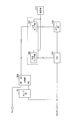
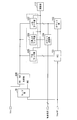
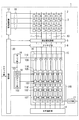
- FIG. 19 is an example of a schematic configuration diagram of a (C) MOS solid-state imaging device according to the third embodiment of the present invention.
- the configuration shown in FIG. 19 will be described below.
- the solid-state imaging device 1 includes an imaging unit 2, a vertical selection unit 12, a readout current source unit 5, an analog unit 6, a clock generation unit 18, a lamp unit 19, a column processing unit 15, a horizontal selection unit 14, an output unit 17, and a control unit. It consists of 20.
- the imaging unit 2 includes a plurality of unit pixels 3 that generate and output a signal corresponding to the magnitude of an incident electromagnetic wave in a matrix.
- the vertical selection unit 12 selects each row of the imaging unit 2.
- the read current source unit 5 reads the signal from the imaging unit 2 as a voltage signal.
- the clock generator 18 generates each clock.
- the ramp unit 19 generates a reference signal (ramp wave) that increases or decreases over time.
- the column processing unit 15 is connected to the lamp unit 19 via a reference signal line 119.
- the horizontal selection unit 14 reads the AD-converted data to the horizontal signal line 118.
- the output unit 17 is connected to the horizontal signal line 118.
- the control unit 20 controls each unit.
- the imaging unit 2 composed of unit pixels 3 of 4 rows ⁇ 6 columns is described. However, in reality, there are several tens of rows and columns in the imaging unit 2. Tens of thousands of unit pixels 3 are arranged.
- the unit pixel 3 constituting the imaging unit 2 is configured by a photoelectric conversion element such as a photodiode / photogate / phototransistor and a transistor circuit.
- peripheral drive systems and signal processing systems that drive and control each unit pixel 3 of the imaging unit 2, that is, a vertical selection unit 12, a horizontal selection unit 14, a column processing unit 15, an output unit 17, and a clock generation unit 18
- Peripheral circuits such as the lamp unit 19 and the control unit 20 are formed integrally with the imaging unit 2 in a semiconductor region such as single crystal silicon using a technique similar to the semiconductor integrated circuit manufacturing technique.
- unit pixels 3 are arranged two-dimensionally by 4 rows and 6 columns, and row control lines 11 are wired for each row with respect to the pixel array of 4 rows and 6 columns.
- Each one end of the row control line 11 is connected to each output end corresponding to each row of the vertical selection unit 12.
- the vertical selection unit 12 includes a shift register or a decoder, and controls the row address and row scanning of the imaging unit 2 via the row control line 11 when driving each unit pixel 3 of the imaging unit 2.
- a vertical signal line 13 is wired for each column with respect to the pixel array of the imaging unit 2.
- FIG. 20 shows an example of the read current source unit 5.
- the read current source unit 5 is configured using NMOS transistors.
- the vertical signal line 13 from the imaging unit 2 is connected to the drain terminal, a desired voltage is appropriately applied to the control terminal, and the source terminal is connected to GND. As a result, a signal from the pixel is output as a voltage mode.
- an NMOS transistor is used as the read current source section 5 is described, but the present invention is not limited to this.
- the column processing unit 15 has an ADC unit 16 provided for each pixel column of the imaging unit 2, that is, for each vertical signal line 13, and is read from each unit pixel 3 of the imaging unit 2 through the vertical signal line 13 for each pixel column.
- the analog pixel signal is converted into digital data.
- the ADC unit 16 is arranged with a one-to-one correspondence with the pixel column of the imaging unit 2, but this is only an example and is limited to this arrangement relationship. is not.
- one ADC unit 16 may be arranged for a plurality of pixel columns, and the one ADC unit 16 may be used in a time-sharing manner between the plurality of pixel columns.
- the ramp unit 19 is configured by, for example, an integration circuit, and generates a so-called ramp wave whose level changes in an inclined manner as time elapses according to control by the control unit 20, and the comparator unit 108 via the reference signal line 119 generates a so-called ramp wave. Supply to one of the input terminals.
- the ramp unit 19 is not limited to the one using an integration circuit, and a DAC circuit may be used. However, in the case of adopting a configuration in which a ramp wave is generated digitally using a DAC circuit, it is necessary to make the step of the ramp wave fine or a configuration equivalent thereto.
- the horizontal selection unit 14 includes a shift register or a decoder, and controls the column address and column scanning of the ADC unit 16 of the column processing unit 15. According to the control by the horizontal selection unit 14, the digital data AD-converted by the ADC unit 16 is sequentially read out to the horizontal signal line 118.
- the control unit 20 may be provided as a separate semiconductor integrated circuit independent of other functional elements such as the imaging unit 2, the vertical selection unit 12, and the horizontal selection unit 14.
- an imaging device which is an example of a semiconductor system is constructed by the imaging device including the imaging unit 2, the vertical selection unit 12, the horizontal selection unit 14, and the like and the control unit 20.
- This imaging apparatus may be provided as an imaging module in which peripheral signal processing, a power supply circuit, and the like are also incorporated.
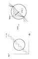
- the clock generation unit 18 includes a VCO 101 and a count unit 103. If the VCO 101 is composed of, for example, nine stages of delay units, the clock generator 18 outputs nine-phase clocks CK0, CK1, CK2, CK3, CK4, CK5, CK6, CK7, and CK8.
- the output unit 17 includes a calculation unit, performs code conversion such as binarization based on the output digital data, and outputs binarized digital data.
- the output unit 17 may include a signal processing function such as black level adjustment, column variation correction, and color processing.
- n-bit parallel digital data may be converted into serial data and output.
- the ADC unit 16 compares the analog pixel signal read from each unit pixel 3 of the imaging unit 2 through the vertical signal line 13 with the ramp wave supplied from the ramp unit 19 for AD conversion, thereby setting the reset level.
- a pulse signal having a magnitude (pulse width) in the time axis direction corresponding to each magnitude of (reference level) and signal level is generated.
- AD conversion is performed by using data corresponding to the pulse width period of the pulse signal as digital data corresponding to the magnitude of the pixel signal.
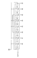
- the ADC unit 16 is provided for each column, and in FIG. 19, six ADC units 16 are provided.
- the ADC units 16 in each column have the same configuration.
- the ADC unit 16 includes a comparison unit 108, a first latch unit 116 including a first lower latch unit 105 and a first upper latch unit 107, a second lower latch unit 105 ′, and a second upper latch unit 107.
- the second latch unit 116 ′ includes the latch unit 107 ′.
- the comparison unit 108 compares the signal voltage corresponding to the analog pixel signal output from the unit pixel 3 of the imaging unit 2 through the vertical signal line 13 with the ramp wave supplied from the ramp unit 19 to thereby generate a pixel signal. Is converted into information in the time axis direction (pulse width of the pulse signal).
- the comparison output of the comparison unit 108 becomes, for example, a high level when the lamp voltage is higher than the signal voltage, and becomes a low level when the lamp voltage is lower than the signal voltage.
- the first latch unit 116 receives the comparison output of the comparison unit 108, and latches the digital data that is the logic state generated by the clock generation unit 18 (VCO 101 and count unit 103) at the timing when the comparison output is inverted. (Hold / store). The digital data latched by the first latch unit 116 is transferred to the second latch unit 116 '.
- the digital data of the lower latch unit 105 and the lower latch unit 105 ' is, for example, 9-bit data.
- the 10 bits are merely an example, and the number of bits may be less than 10 bits (for example, 8 bits) or the number of bits may be more than 10 bits (for example, 12 bits).
- the ADC unit 16 has a configuration in which the latch unit 116 and the latch unit 116 ′ are arranged separately in the vertical direction, but this is only an example. For example, in order to shorten the transfer time, it is preferable to arrange the corresponding bits of the corresponding latch unit close to each other.
- the unit pixel 3 outputs a reset level and a signal level.
- AD conversion is performed as follows. For example, a ramp wave that falls at a predetermined inclination is compared with a reset level or each signal level voltage that is a pixel signal from the unit pixel 3, and the reset level or The period until the signal corresponding to the signal level matches the ramp wave (ramp voltage) is counted by the clock (for example, CK8) output from the VCO 101, and multiphase clocks (CK0, CK1 having a certain phase difference) , CK2, CK3, CK4, CK5, CK6, CK7, CK8), the digital state corresponding to each magnitude of the reset level or signal level is obtained.
- the clock for example, CK8
- the reset level including the noise of the pixel signal is read out as an analog pixel signal in the first reading operation, and then in the second reading operation.
- the signal level is read out.
- the reset level and the signal level are input to the ADC unit 16 through the vertical signal line 13 in time series.
- the control unit 20 supplies the ramp unit 19 with control data for ramp wave generation.
- the ramp unit 19 outputs a ramp wave whose waveform changes in a ramp shape as a whole as a comparison voltage applied to one input terminal of the comparison unit 108.
- the comparison unit 108 compares this ramp wave with the reset level.
- the logical states of the VCO 101 and the count unit 103 are output to the lower latch unit 105 and the upper latch unit 107 constituting the first latch unit 116.
- the comparison unit 108 compares the ramp wave supplied from the ramp unit 19 with the reset level, and inverts the comparison output when the voltages of both are substantially the same.
- the first latch unit 116 holds the logical states of the VCO 101 and the count unit 103 at the time when the comparison output is inverted in the lower latch unit 105 and the upper latch unit 107.
- the control unit 20 stops supplying control data to the ramp unit 19 and outputting from the clock generation unit 18.
- the ramp unit 19 stops generating the ramp wave.
- the data held in the first latch unit 116 is transferred to the second latch unit 116 '.
- the data held in the lower latch unit 105 is transferred to the lower latch unit 105 ′
- the data held in the upper latch unit 107 is transferred to the upper latch unit 107 ′.
- ⁇ Second reading> Subsequently, at the time of the second reading, a signal level corresponding to the amount of incident light for each unit pixel 3 is read, and the same operation as the first reading is performed.
- the control unit 20 supplies the ramp unit 19 with control data for ramp wave generation.
- the ramp unit 19 outputs a ramp wave whose waveform changes in a ramp shape as a whole as a comparison voltage applied to one input terminal of the comparison unit 108.
- the comparison unit 108 compares the ramp wave with the signal level.
- the logical states of the VCO 101 and the count unit 103 are output to the lower latch unit 105 and the upper latch unit 107 constituting the first latch unit 116.
- the comparison unit 108 compares the ramp wave supplied from the ramp unit 19 with the signal level, and inverts the comparison output when the voltages of both are substantially the same.
- the first latch unit 116 holds the logical states of the VCO 101 and the count unit 103 at the time when the comparison output is inverted in the lower latch unit 105 and the upper latch unit 107.
- the control unit 20 stops supplying control data to the ramp unit 19 and outputting from the clock generation unit 18. As a result, the ramp unit 19 stops generating the ramp wave.
- the digital data latched by the first latch unit 116 and the second latch unit 116 ′ is output via the horizontal signal line 118 by the horizontal selection unit 14 and transferred to the arithmetic unit built in the output unit 17. .
- the arithmetic unit performs binarization processing and subtraction processing (difference processing between the reset level data and the signal level data) to obtain combined signal component data.
- a lower logical state composed of a multiphase clock having a constant phase difference is set as a lower bit, and a higher logical state generated by using one of the multiphase clocks as a count clock. Is the upper bit.
- the logic state of the multiphase clock when the comparison output between the analog pixel signal and the ramp wave is inverted is held. Thereby, it becomes possible to obtain a bit string having finer time information without being restricted by the operation speed of the counter.
- the differential processing between the reset level data and the signal level data makes it possible to perform AD conversion of the signal component at high speed and with high accuracy.
- the signal level data is latched by the first latch unit 116, so that the reset level and the signal level are latched. Is latched by the same first latch unit 116, so that it is possible to suppress a data hold error due to an individual difference in characteristics of each latch unit.
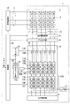
- FIG. 21 is an example of a schematic configuration diagram of a (C) MOS solid-state imaging device according to the fourth embodiment of the present invention.
- the configuration diagram shown in FIG. 21 will be described below.
- the difference from FIG. 19 is that the first redundant upper latch unit 106 and the second redundant upper latch unit 106 ′ for holding the redundant upper logical state obtained by delaying the upper logical state from the count unit 103 by a certain delay time. It is to have established. Other than that, it is the same as FIG.
- the upper logical state and the redundant upper logical state obtained by delaying the upper logical state can be output. Therefore, for example, at the timing of holding data between the lower logical state and the upper logical state. Even when a deviation (mismatch) occurs, it is possible to correct the data by using data holding the redundant upper logical state.
- FIG. 22 is an example of a schematic configuration diagram of a (C) MOS solid-state imaging device according to the fifth embodiment of the present invention.
- a comparison delay unit 109 is provided which outputs the comparison output of the comparison unit 108 after being delayed by a certain delay time.
- FIG. 21 A difference from FIG. 21 is that a comparison delay unit 109 is provided which outputs the comparison output of the comparison unit 108 after being delayed by a certain delay time. Other than that, it is the same as FIG.
- the upper logical state and the redundant upper logical state obtained by delaying the upper logical state can be output. Therefore, for example, at the timing of holding data between the lower logical state and the upper logical state. Even when a deviation (mismatch) occurs, it is possible to correct the data by using data holding the redundant upper logical state. Further, in addition to outputting the comparison result in the comparison unit 108, the comparison result can be output after being delayed by a certain delay time, so that the data fetch timing is controlled as a result, and the fetch timing is more suitable. It becomes possible.
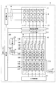
- FIG. 23 is an example of a schematic configuration diagram of a (C) MOS solid-state imaging device according to the sixth embodiment of the present invention.
- the configuration shown in FIG. 23 will be described below.
- 19 is different from FIG. 19 in that the counting unit 103 is incorporated in each ADC unit 16 as a column counter 103 ′, and the comparison delay unit 109 for delaying and outputting the comparison result of the comparison unit 108 by a certain delay time is provided.
- the first redundant upper latch unit 106 and the second redundant upper latch unit 106 ′ are provided for holding the redundant upper logical state obtained by delaying the upper logical state from the count unit 103 by a certain delay time. Other than that, it is the same as FIG.
- the column counter 103 ′ is assumed to be a counter circuit having a latch function for holding the upper logical state. This eliminates the need to separately incorporate the first higher-order latch unit.
- the column counter 103 ′ may be configured using an Up / Down counter circuit. In that case, since the number of built-in latch circuits can be reduced, the area can be reduced.
- AD conversion is performed as follows. For example, a ramp wave that falls at a predetermined inclination is compared with a reset level or each signal level voltage that is a pixel signal from the unit pixel 3, and the reset level or The period until the signal corresponding to the signal level matches the ramp wave (ramp voltage) is counted by the clock (for example, CK8) output from the VCO 101, and multiphase clocks (CK0, CK1 having a certain phase difference) , CK2, CK3, CK4, CK5, CK6, CK7, CK8), the digital state corresponding to each magnitude of the reset level or signal level is obtained.
- the clock for example, CK8
- the reset level including the noise of the pixel signal is read out as an analog pixel signal in the first reading operation, and then in the second reading operation.
- the signal level is read out.
- the reset level and the signal level are input to the ADC unit 16 through the vertical signal line 13 in time series.
- the control unit 20 supplies the ramp unit 19 with control data for ramp wave generation.
- the ramp unit 19 outputs a ramp wave whose waveform changes in a ramp shape as a whole as a comparison voltage applied to one input terminal of the comparison unit 108.
- the comparison unit 108 compares this ramp wave with the reset level.
- the lower logical state of the VCO 101 is held in the lower latch unit 105 constituting the first latch unit 116.
- One of the clocks in the lower logical state is used as a count clock for the column counter 103 ′.
- the comparison unit 108 compares the ramp wave supplied from the ramp unit 19 with the reset level, and inverts and outputs the comparison output when both voltages substantially coincide. This output timing is defined as a first timing. Further, the comparison delay unit 109 delays the comparison output from the comparison unit 108 by a certain delay time and outputs it. This output timing is defined as a second timing.
- the redundant upper logical state of the column counter 103 ′ is held in the redundant upper latch unit 106.
- the lower logical state of the VCO 101 is held in the lower latch unit 105, and the column counter 103 'holds the upper logical state by stopping the counting operation of the column counter 103', for example.
- the control unit 20 stops supplying control data to the ramp unit 19 and outputting from the clock generation unit 18.
- the ramp unit 19 stops generating the ramp wave.
- the data held in the first latch unit 116 is transferred to the second latch unit 116 '.
- the data held in the lower latch unit 105 is transferred to the lower latch unit 105 ′, the data held in the column counter 103 ′ is transferred to the upper latch unit 107 ′, and held in the redundant upper latch unit 106 The transferred data is transferred to the redundant upper latch unit 106 ′.
- the control unit 20 supplies the ramp unit 19 with control data for ramp wave generation.
- the ramp unit 19 outputs a ramp wave whose waveform changes in a ramp shape as a whole as a comparison voltage applied to one input terminal of the comparison unit 108.
- the comparison unit 108 compares the ramp wave with the signal level.
- the lower logical state of the VCO 101 is held in the lower latch unit 105 constituting the first latch unit 116.
- One of the clocks in the lower logical state is used as a count clock for the column counter 103 ′.
- the comparison unit 108 compares the ramp wave given from the ramp unit 19 with the signal level, and inverts and outputs the comparison output when the two voltages substantially coincide. This output timing is defined as a first timing. Further, the comparison delay unit 109 delays the comparison output from the comparison unit 108 by a certain delay time and outputs it. This output timing is defined as a second timing.
- the redundant upper logical state of the column counter 103 ′ is held in the redundant upper latch unit 106.
- the lower logical state of the VCO 101 is held in the lower latch unit 105, and the column counter 103 'holds the upper logical state by stopping the counting operation of the column counter 103', for example.
- the control unit 20 stops supplying control data to the ramp unit 19 and outputting from the clock generation unit 18.
- the ramp unit 19 stops generating the ramp wave.
- ⁇ Calculation processing> The digital data held in the first latch unit and the second latch unit is output via the horizontal signal line 118 by the horizontal selection unit 14 and transferred to the calculation unit built in the output unit 17. Thereafter, the arithmetic unit performs binarization processing and subtraction processing to obtain combined data of signal components.
- a lower logical state composed of a multiphase clock having a constant phase difference is set as a lower bit, and a higher logical state generated by using one of the multiphase clocks as a count clock. Is the upper bit.
- the logic state of the multiphase clock when the comparison output between the analog pixel signal and the ramp wave is inverted is held. Thereby, it becomes possible to obtain a bit string having finer time information without being restricted by the operation speed of the counter.
- the redundant upper logical state is maintained even when a deviation (mismatch) occurs in the timing of retaining data between the lower logical state and the upper logical state, for example.
- a deviation mismatch
- the column counter 103 ′ When the column counter 103 ′ is configured by using the Up / Down counter circuit, the column counter 103 ′ performs counting, for example, by down-counting at the time of the first reading, and counting by, for example, up-counting at the time of the second reading. Good. As a result, the CDS operation of the upper data of the reset level and the upper data of the signal level becomes possible.
- an AD converter that can perform AD conversion with higher accuracy and a solid-state imaging device using the AD converter can be provided.
Landscapes
- Engineering & Computer Science (AREA)
- Theoretical Computer Science (AREA)
- Multimedia (AREA)
- Signal Processing (AREA)
- Analogue/Digital Conversion (AREA)
- Transforming Light Signals Into Electric Signals (AREA)
Abstract
このAD変換器において、ランプ部(19)は、時間の経過とともに増加または減少する参照信号を生成する。比較部(108)は、アナログ信号の入力に係るタイミングでアナログ信号と参照信号の比較処理を開始し、参照信号がアナログ信号に対して所定の条件を満たしたタイミングで比較処理を終了する。VCO(101)は、複数の同一構成の遅延ユニットを有し、比較処理の開始に係るタイミングで遷移動作を開始する。カウント部(103)は、VCO(101)からのクロックをカウントする。下位ラッチ部(105)は、比較処理の終了に係る第1のタイミングで、複数の遅延ユニットの論理状態である下位論理状態をラッチする。上位ラッチ部(107)は、上記第1のタイミングで、カウント部(103)の論理状態である上位論理状態をラッチする。演算部(117)は、下位ラッチ部(105)および上位ラッチ部(107)のデータに基づいてデジタル信号を算出する。このAD変換器によれば、より高精度なAD変換が可能となる。
Description
AD変換器(アナログ-デジタル変換器)およびそれを用いた固体撮像装置に関する。
本願は、2009年9月1日に日本に出願された特願2009-201522号に基づき優先権を主張し、その内容をここに援用する。
本願は、2009年9月1日に日本に出願された特願2009-201522号に基づき優先権を主張し、その内容をここに援用する。
従来例に係るAD変換器を用いた一例として、特許文献1~4に記載された構成が知られている。初めに、特許文献1のAD変換器の構成および動作について説明する。
図24は、特許文献1に記載された第1の従来例に係るAD変換器を用いたMOSセンサの構成図である。このMOSセンサは、画素1101の列毎に、比較器1107およびデジタルメモリ1108で構成されたAD変換回路1106を備えている。カウンタ1104から出力されるデジタル(バイナリ)値は、DA変換回路(以後、DACと称す)1105に入力される。DAC1105は、入力されたデジタル値に応じたランプ電圧(ランプ波)1122を生成し、このランプ電圧(ランプ波)1122を参照信号として比較器1107の入力部の一方に出力する。カウンタ1104の出力は、バイナリ→グレイコード変換器1115を介して各列のデジタルメモリ1108に分配される。各AD変換回路1106内の比較器1107の入力部の他方には、画素1101から読出し信号線1103を介して画素信号が、AD変換の対象となるアナログ信号として入力される。
次に、第1の従来例に係るAD変換動作を説明する。まず、クロック生成回路1120から入力されるクロック信号1121に同期して、カウンタ1104がその初期値からカウントを開始するのと同時に、DAC1105がランプ電圧(ランプ波)1122の生成を開始する。そして、各列の画素1101からの読出し信号と、カウンタ1104の計数値と同期して変化する共通のランプ電圧(ランプ波)1122とが各列の比較器1107に入力される。これと平行して、カウンタ1104の計数値はデジタルメモリ1108に分配される。ある列の比較器1107への2つの入力信号の大小関係が入れ替わると、その比較器1107の出力電圧が反転し、その列のデジタルメモリ1108はその計数値を保持する。比較器1107に入力されるランプ電圧(ランプ波)1122とデジタルメモリ1108に入力される計数値は同期しているので、以上の動作により、画素からの読出し信号が、デジタルメモリに保持された値(デジタル値)にAD変換される。
以上で説明したAD変換方式は、特にランプ型AD変換(Ramp Run-up ADC)と呼ばれる種類の方式で、AD変換一般の方式分類によると、カウンティングADC(計数型AD変換)と呼ばれる種類の方式である。参照信号としてランプ電圧(ランプ波)を用いることは、画素からのアナログ信号電位を時間の長さに変換するのと等価であり、更に固定周波数のクロック信号を用いて時間の長さを計ることでAD変換を実現するため、この名称がある。
特許文献2~4に記載された第2の従来例に係るAD変換器では、カウンタ1104の計数値を上位ビットとし、更にカウンタに入力されるクロック(またはカウンタから出力されるクロック)の位相を遅延させることにより多相クロックを生成して、その論理状態を下位ビットとすることで更なる分解能の向上を可能としている。
第1の従来例に係るAD変換器を用いて、例えば10ビットのAD変換を実現する場合、AD変換の対象となるアナログ信号とDACで生成されるランプ電圧(ランプ波)との比較では、10ビットの階調数分(すなわち1024回)のカウントを行う必要がある。
ここで、AD変換器を用いる具体的なデバイスとして、デジタルスチルカメラ(DSC)等に使用されるイメージャを例示する。具体的なスペックとしては、画素数は2000万画素、フレームレートは60frame/secとする。説明を容易にするため、2000万画素の画素配列を縦横比4000行×5000列として、更に単純化のためにブランキング期間がないものとすると、1行の読出し期間は、
60frame/sec×4000行/frame=240Kline/sec
となる。つまり、1行の読出しレートは240KHzとなる。このデバイスに第1の従来例に係るAD変換器を適用すると、10ビットのAD変換であれば、1行の読出し時間にその階調数210=1024回の比較をする必要があり、1行の読出しレートの約千倍である240MHz程度で、デジタルメモリに出力するカウンタの計数値を変える必要がある。
60frame/sec×4000行/frame=240Kline/sec
となる。つまり、1行の読出しレートは240KHzとなる。このデバイスに第1の従来例に係るAD変換器を適用すると、10ビットのAD変換であれば、1行の読出し時間にその階調数210=1024回の比較をする必要があり、1行の読出しレートの約千倍である240MHz程度で、デジタルメモリに出力するカウンタの計数値を変える必要がある。
この計算では、AD変換回路が画素からデータを受け取るまでの待機期間やAD変換結果の出力メモリへの転送期間、すなわちAD変換としての比較動作ができない期間を考慮していない。また、上記以外にOB(=Optical Black)画素期間やブランキング期間を除いているため、実際には、この見積り周波数よりも高い周波数になる。
次に、第2の従来例に係るAD変換器を用いて、同様な計算をしてみる。例えば10ビットを上位8ビットと下位2ビットで構成したとすると、上位ビットについては、1行の読出しレートの256倍である60MHz程度で、デジタルメモリに出力するカウンタの計数値を変えるだけで済む。下位ビットについては、カウンタに入力するクロック(またはカウンタから出力されるクロック)の位相を0、π/4、π/2、3π/4、と遅延させ、その論理状態を保持およびエンコードすることによりデジタル値を取得する。更に、10ビットを上位6ビットと下位4ビットで構成したと仮定すると、上位ビットについては、1行の読出しレートの64倍である15MHz程度で、デジタルメモリに出力するカウンタの計数値を変えるだけで済む。下位ビットについては、カウンタに入力するクロック(またはカウンタから出力されるクロック)の位相を0、π/16、π/8、3π/16、π/4、5π/16、3π/8、7π/16、π/2、9π/16、5π/8、11π/16、3π/4、13π/16、7π/8、15π/16、と遅延させ、その論理状態を保持およびエンコードすることによりデジタル値を取得する。
しかしながら、上記従来のAD変換器には以下に示すような、AD変換の精度に関する課題がある。
(1)上位ビットと下位ビットとが完全な従属動作ではない。
(2)下位ビットの保持データを正確に2値化するのが困難である。
(1)上位ビットと下位ビットとが完全な従属動作ではない。
(2)下位ビットの保持データを正確に2値化するのが困難である。
以下で、上記(1)の不具合について詳述する。仮に、上位ビットおよび下位ビットのラッチタイミングが同じであったとしても、上位ビットと下位ビットとが完全に従属していないため、例えば下位ビットの論理状態が変化する前に上位ビットの論理状態が変化する、逆に上位ビットの論理状態が変化する前に下位ビットの論理状態が変化する、所謂上位ビットと下位ビットとの間での位相ズレが存在し、特に高速動作になるとこの位相ズレが顕著に(相対的に大きく)見えてくる。これにより、上位ビットと下位ビットとの位相ズレに起因したミスコードが発生し、精度の高いAD変換結果を得ることができない。
次に、上記(2)の不具合について詳述する。下位ビットの2値化は、デジタルメモリに保持された多相クロックの論理状態に基づいて行われる。特に高速動作におけるラッチタイミングでの論理状態の取得の際には、[1]High状態からLow状態へ論理状態が変化する途中のLow状態や、[2]Low状態からHigh状態へ論理状態が変化する途中のHigh状態が混在する(確率が高くなる)。これが2値化を困難にしている。2値化が困難である第1の理由は、回路の立上り時間と立下り時間とは必ずしも等しくならない、ことに起因する。CMOS回路、例えばCMOSインバータ回路で考えた場合、PMOSトランジスタの閾値電圧の設定とNMOSトランジスタの閾値電圧の設定とは、異なる工程で行われる。また、回路の出力電圧の立上り時間は、主としてPMOSトランジスタの閾値電圧によって決定され、回路の立下り時間は、主としてNMOSトランジスタの閾値電圧によって決定される。したがって、回路の出力電圧の立上り時間と立下り時間とが異なるのは、特別な現象ではなく、製造工程に由来して起こる一般的な現象である。2値化が困難である第2の理由は、仮に、立上り時間と立下り時間とが等しくなるよう製造できたとしても、実際には電源電圧変動や温度変化によって保持回路(ラッチ回路)の閾値電圧が変動するため、結果的に誤った論理状態を保持する可能性がある、ことに起因する。この問題を回避するためには、電源電圧変動や温度変化を検知して回路を制御する手段を内蔵することが必要となるが、その分、回路規模が大きくなり、消費電力も増大する。
本発明は、上述した課題に鑑みてなされたものであって、より高精度にAD変換することができるAD変換器およびそれを用いた固体撮像装置を提供することを目的とする。
本発明のAD変換器は、時間の経過とともに増加または減少する参照信号を生成する参照信号生成部と、AD変換の対象となるアナログ信号の入力に係るタイミングで前記アナログ信号と前記参照信号の比較処理を開始し、前記参照信号が前記アナログ信号に対して所定の条件を満たしたタイミングで前記比較処理を終了する比較部と、複数の同一構成の遅延ユニットを有し、前記比較処理の開始に係るタイミングで遷移動作を開始する円環遅延回路と、前記円環遅延回路からのクロックをカウントするカウント部と、前記比較処理の終了に係る第1のタイミングで、前記複数の遅延ユニットの論理状態である下位論理状態をラッチする下位ラッチ部と、前記比較処理の終了に係る前記第1のタイミングで、前記カウント部の論理状態である上位論理状態をラッチする上位ラッチ部と、前記下位ラッチ部および前記上位ラッチ部のデータに基づいて前記アナログ信号に応じたデジタル信号を算出する演算部と、を有する。
また、本発明のAD変換器において、前記複数の遅延ユニットの個数は、奇数個である、ことが望ましい。
また、本発明のAD変換器において、前記複数の遅延ユニットの個数は、奇数個であり、前記複数の遅延ユニットの各々は、更に奇数個の反転素子を有する、ことが望ましい。
また、本発明のAD変換器において、前記遅延ユニットを構成する前記奇数個の前記反転素子は全差動型反転回路で構成される、ことが望ましい。
また、本発明のAD変換器において、前記複数の遅延ユニットは、その遅延量を制御可能となるよう構成される、ことが望ましい。
また、本発明のAD変換器において、前記複数の遅延ユニットの遅延量は、遅延ユニットに流れる電流により制御される、ことが望ましい。
また、本発明のAD変換器において、前記演算部は、前記複数の遅延ユニットからの出力である前記下位ラッチ部のデータを、一定の時間間隔で順に立上る、又は、一定の時間間隔で順に立下る信号群に並び変え、前記演算部は、前記比較処理の終了に係る前記第1のタイミングでの前記信号群における状態の遷移位置を検出する、ことが望ましい。
また、本発明のAD変換器において、前記カウント部は、前記上位論理状態以外に冗長上位論理状態を出力し、ラッチ部として前記下位ラッチ部および前記上位ラッチ部以外に、前記冗長上位論理状態をラッチする冗長上位ラッチ部を有し、前記冗長上位論理状態は前記上位論理状態の少なくとも一部をある時間だけ遅延させたものである、または前記上位論理状態は前記冗長上位論理状態の少なくとも一部をある時間だけ遅延させたものである、ことが望ましい。
また、本発明のAD変換器において、前記比較部は、前記比較処理の終了に係る前記第1のタイミングを示す信号と、前記第1のタイミングをある遅延時間だけ遅延させた第2のタイミングを示す信号とを出力する、ことが望ましい。
また、本発明のAD変換器において、前記参照信号生成部は、積分回路を用いて構成される、ことが望ましい。
また、本発明のAD変換器において、前記参照信号生成部は、DAC回路を用いて構成される、ことが望ましい。
また、本発明のAD変換器において、前記参照信号生成部は、前記DAC回路の後段に更にLPF回路を有する、ことが望ましい。
また、本発明のAD変換器において、前記LPF回路のフィルタ定数は、少なくとも前記遅延ユニットの遅延量および前記DAC回路の量子化ステップ、に応じて制御される、ことが望ましい。
また、本発明は、入射される電磁波の大きさに応じて画素信号を出力する画素が複数、行列状に配された撮像部と、前記画素信号に応じたアナログ信号をAD変換の対象となるアナログ信号とする前記AD変換器と、前記撮像部および前記AD変換器を制御する制御部と、を有する固体撮像装置である。
また、本発明の固体撮像装置において、前記画素信号は、基準レベルと信号レベルとを含んでおり、前記比較部は、前記基準レベルと前記参照信号とを比較する第1の比較処理と、前記信号レベルと前記参照信号とを比較する第2の比較処理とを実行し、前記上位ラッチ部は、第1の上位ラッチ部および第2の上位ラッチ部を有し、前記下位ラッチ部は、第1の下位ラッチ部および第2の下位ラッチ部を有し、前記第1の比較処理に係る第1のデータと、前記第2の比較処理に係る第2のデータと、を保持する、ことが望ましい。
また、本発明の固体撮像装置において、前記第1のデータを前記第1の上位ラッチ部および前記第1の下位ラッチ部に保持し、保持された第1のデータを前記第2の上位ラッチ部および前記第2の下位ラッチ部に転送した後、前記第2のデータを前記第1の上位ラッチ部および前記第1の下位ラッチ部に保持する、ことが望ましい。
また、本発明の固体撮像装置において、前記カウント部は、前記上位論理状態以外に、更に前記冗長上位論理状態を出力し、前記上位ラッチ部は、前記第1の上位ラッチ部および前記第2の上位ラッチ部以外に、更に第1の前記冗長上位ラッチ部および第2の前記冗長上位ラッチ部を有し、前記下位ラッチ部は、第1の下位ラッチ部および第2の下位ラッチ部を有する、ことが望ましい。
また、本発明の固体撮像装置において、前記第1のデータを前記第1の上位ラッチ部、前記第1の冗長上位ラッチ部、および前記第1の下位ラッチ部に保持し、保持されたデータを前記第2の上位ラッチ部、前記第2の冗長上位ラッチ部、および前記第2の下位ラッチ部に転送した後、前記第2のデータを前記第1の上位ラッチ部、前記第1の冗長上位ラッチ部、および前記第1の下位ラッチ部に保持する、ことが望ましい。
また、本発明の固体撮像装置において、前記第1あるいは前記第2の上位ラッチ部でのデータの保持は、前記比較処理の終了に係る前記第1のタイミングまたは前記比較処理の終了に係る前記第1のタイミングをある遅延時間だけ遅延させた前記第2のタイミングの一方で行い、前記第1あるいは前記第2の冗長上位ラッチ部のデータ保持は、前記比較処理の終了に係る前記第1のタイミングまたは前記比較処理の終了に係る前記第1のタイミングをある遅延時間だけ遅延させた前記第2のタイミングの他方で行う、ことが望ましい。
また、本発明の固体撮像装置において、前記撮像部の1列、または複数列毎に前記カウント部を設けてカラムカウント部とし、前記円環遅延回路からのクロックを、前記カラムカウント部のカウントクロックとして用いる、ことが望ましい。
また、本発明の固体撮像装置において、前記カラムカウント部は、アップカウントモードおよびダウンカウントモードを有し、前記第1の比較処理に係るカウントをダウンカウントまたはアップカウントの一方で行い、前記第2の比較処理に係るカウントをダウンカウントまたはアップカウントの他方で行う、ことが望ましい。
本発明によれば、上位論理状態と下位論理状態が、同一の円環遅延回路の出力に基づくことにより上位論理状態と下位論理状態の位相関係が保たれるので、より高精度にAD変換することができる。
また、本発明によれば、下位ラッチ部のデータを、一定の時間間隔で順に立上る、又は、一定の時間間隔で順に立下る信号群に並び変え、比較処理の終了に係る第1のタイミングでの信号群における状態の遷移位置を検出することにより、信号の立上りあるいは立下りのみを基準に遷移位置を検出することが可能となるので、より高精度にAD変換することができる。
以下、本発明の実施形態について図を参照しながら説明する。
(第1の実施形態)
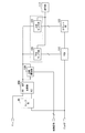
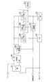
図1は、本発明の第1の実施形態によるAD変換器全体の構成図の一例である。以下、図1に示す構成について説明する。このAD変換器は、ランプ部19、比較部108、VCO101、カウント部103、下位ラッチ部105、上位ラッチ部107、演算部117で構成される。
図1は、本発明の第1の実施形態によるAD変換器全体の構成図の一例である。以下、図1に示す構成について説明する。このAD変換器は、ランプ部19、比較部108、VCO101、カウント部103、下位ラッチ部105、上位ラッチ部107、演算部117で構成される。
ランプ部19は、時間の経過とともに増加または減少する参照信号(ランプ波)を生成する。比較部108は、AD変換の対象となるアナログ信号Vinが入力される第1の入力端子IN1と、ランプ部19からのランプ波が入力される第2の入力端子IN2と、その比較結果を出力する第3の端子OUTとを有する。VCO101は、n個の(nは2以上の自然数)遅延ユニット(Delay Unit)を有する円環遅延回路である。カウント部103は、VCO101からのクロックをカウントする。下位ラッチ部105は、VCO101の下位論理状態を保持する。上位ラッチ部107は、カウント部103の上位論理状態を保持する。演算部117は、下位ラッチ部105および上位ラッチ部107のデータに基づいてデジタル信号を算出する。
次に、本例の動作について説明する。まず、スタートパルス(StartP)の論理状態がLowからHighに変化することで、VCO101が遷移動作を開始するとともにカウント部103がその初期値からカウントを開始する。これと同時に、ランプ部19がランプ波の生成を開始する。そして、AD変換の対象となるアナログ信号Vinと、カウント部103の上位論理状態と略同期して変化(増加あるいは減少)するランプ波とが比較部108に入力され、比較部108は比較動作を開始する。
これと平行して、VCO101の下位論理状態は下位ラッチ部105に、カウント部103の上位論理状態は上位ラッチ部107に、それぞれ分配される。比較部108への2つの入力信号の大小関係が入れ替わると、比較部108の出力が反転し、下位ラッチ部105および上位ラッチ部107は各々、入力される論理状態を保持する。比較部108に入力されるランプ波と下位ラッチ部105および上位ラッチ部107に入力される論理状態は略同期しているので、AD変換の対象となるアナログ信号が、下位ラッチ部105および上位ラッチ部107に保持された値にAD変換されることになる。その後、演算部117において下位ラッチ部105および上位ラッチ部107のデータから合成データが算出される。
図2は、図1のVCO101の構成図の一例である。VCO101は、遅延ユニット(Delay Unit)を円環状に奇数段(本例では9段)接続した構成となっている。遅延ユニットDU0~DU8は、動作中の遅延ユニットの状態CK0~CK8を各出力端子から出力する。ここでは、状態CK8がカウント部103へのクロックとなる。上記では、遅延ユニットの数を9段として説明したが、これに限る必要はない。
図3は、図2の遅延ユニットの部分Dの拡大図を示した第1の例である。各遅延ユニットDU0~DU8は、3個の反転素子(NAND*_1およびINV*_1~INV*_2)で構成される。ここで、『*』には各遅延ユニットDU0~DU8の対応する数字(0~8)が入る。上記では、反転素子の数を3個として説明したが、これに限る必要はない。また、NAND回路とINV(インバータ)回路を用いて遅延ユニットを構成したが、これ以外でも構わない。
図4は、図2の遅延ユニットの部分Dの拡大図を示した第2の例である。各遅延ユニットDU0~DU8は、3個の全差動型反転素子(DE*_1~DE*_3)で構成される。ここで、『*』には各遅延ユニットDU0~DU8の対応する数字(0~8)が入る。上記では、全差動型反転素子の数を3個として説明したが、これに限る必要はない。
図5は、図2の遅延ユニットの部分Dの拡大図を示した第3の例である。図3と異なるのは、各遅延ユニットDU0~DU8を構成する反転素子INV*_1の電源線に、遅延ユニットDU0~DU8の遅延量を制御するための電流源I1およびI2を挿入したことである。これにより、遅延量を可変することが可能となり、VCO101を例えば他のクロックに同期させて動作させる、等のフィードバック動作が可能となる。上記では、反転素子INV*_1の電源線に電流源を挿入して説明したが、これに限る必要はない。
図6は、図2の遅延ユニットの部分Dの拡大図を示した第4の例である。図4と異なるのは、各遅延ユニットDU0~DU8を構成する全差動型反転素子DE*_2の電源線に、遅延ユニットDU0~DU8の遅延量を制御するための電流源I1およびI2を挿入したことである。これにより、遅延量を可変することが可能となり、VCO101を例えば他のクロックに同期させて動作させる、等のフィードバック動作が可能となる。上記では、全差動型反転素子DE*_2の電源線に電流源を挿入して説明したが、これに限る必要はない。
上記のように、VCO101を構成する遅延ユニットDU0~DU8の下位論理状態が下位ラッチ部105に保持され、遅延ユニットDU8の論理状態が入力されるカウント部103の上位論理状態が上位ラッチ部107に保持される。これにより、上位論理状態と下位論理状態は、同一のスタートパルス(StartP)に同期してそれぞれ変化することになり、上位論理状態と下位論理状態の位相関係が保たれるので、前述した(1)の課題を解決することが可能となる。
尚、本構成では円環遅延回路を、対称発振回路であるVCO(=Voltage Controlled Oscillator)回路で構成した場合について説明したが、対称発振回路と同様に円環遅延回路自体は奇数個の遅延ユニットで構成されるが、その出力は等価的に偶数(特に、2のべき乗)である所謂非対称発振回路を用いても構わない。更に、図15に示すような円環遅延回路自体が偶数個(特に、2のべき乗個)の遅延ユニットで構成され、下位論理状態の出力(端子)が偶数(特に、2のべき乗)となるRDL(=Ring Delay Line)回路や円環遅延回路自体が偶数個(特に、2のべき乗個)の遅延ユニットで構成され、更に遅延ユニットを構成する全差動型反転回路の最終段の出力がそれぞれ初段の入力の逆側に帰還されて構成される所謂全差動型発振回路を用いても構わない。
次に、VCO101の下位論理状態の検出動作について、説明する。図7は、下位論理状態の検出動作を説明するための図で、構成図((a))およびタイミングチャート((b))から構成されている。以下、図7の(a)に示す構成について説明する。VCO101は、遅延ユニットを9段接続した構成である。遅延ユニットDU0~DU8は、動作中の遅延ユニットの状態CK0~CK8を各出力端子から出力する。各遅延ユニットDU0~DU8は、NAND回路(NAND0~NAND8)で構成されており、NAND回路(NAND1~NAND8)の一方の端子は電源VDDに接続された構成となっている。
次に、図7の(b)に示す動作について説明する。スタートパルス(StartP)の論理状態がLowからHighに変化するとVCO101の遷移動作が開始され、信号CK0~CK8は一定の時間間隔で反転動作を繰り返すことになる。つまり、VCO101内の遅延ユニットの状態が順次変化(遷移)していく。ここで、演算部117は、VCO101の状態出力(=信号群)を第1の信号群(CK1、CK3、CK5、CK7)と第2の信号群(CK0、CK2、CK4、CK6、CK8)とに分類して並び替える。具体的には、CK1、CK3、CK5、CK7、CK0、CK2、CK4、CK6、CK8、と並び変える。これにより、図7の(b)の矢印が示すように、信号群は一定の時間間隔で順に立上る(又は、一定の時間間隔で順に立下る)ことになる。
続いて、比較処理の終了に係るタイミングで保持されたデータにおける遷移位置の検出が行われる。尚、遷移位置は、並び替えた信号群において状態がLowからHigh(あるいはHighからLow)に変化した箇所である。例えば、図7の(b)において、スタートパルス(StartP)の論理状態がLowからHighに変化してからTs秒後のVCO101の状態出力は、Low(CK1)、Low(CK3)、Low(CK5)、Low(CK7)、High(CK0)、High(CK2)、High(CK4)、High(CK6)、High(CK8)となり、CK0が遷移位置である。上記のように並び替えた信号群においては、状態がLowからHigh(あるいはHighからLow)に変化した遷移位置が時間の経過とともに順次移動する。
この遷移位置の検出回路としては、例えばフラッシュ型ADCと略同様な手法が採れる。例えば、並び替えた信号群においてLowからHigh(あるいはHighからLow)に状態変化した箇所を遷移位置とすることで、遷移位置が検出できる。この遷移位置は、信号の立上りと立下りのうちの一方のみを基準にして検出できるので、前述した(2)の課題を解決することが可能となる。ちなみに、本例の場合、得られる下位ビットのデータは2のべき乗ではないが、上位ビットと下位ビットの合成データを2のべき乗とする場合、詳細は省略するが、加減算およびビットシフト等の簡易な演算処理で容易に2のべき乗のデータに変換することが可能である。尚、前述した出力が等価的に2のべき乗である非対称発振回路等であればこれは必要ない。
次に、VCO101の下位論理状態の検出動作の他の例について、説明する。図8は、下位論理状態の検出動作を説明するための図で、構成図((a))およびタイミングチャート((b))から構成されている。以下、図8の(a)に示す構成について説明する。VCO101は遅延ユニット(Delay Unit)を9段接続した構成である。遅延ユニットDU0~DU8は、動作中の遅延ユニットの状態CK0~CK8および/CK0~/CK8を各出力端子から出力する。各遅延ユニットDU0~DU8は、全差動型反転素子(DE0~DE8)で構成されている。
次に、図8の(b)に示す動作について説明する。スタートパルス(StartP)の論理状態がLowからHighに変化するとVCO101の発振が開始され、信号CK0~CK8および/CK0~/CK8は一定の時間間隔で反転動作を繰り返すことになる。つまり、VCO101内の遅延ユニットの状態が順次変化(遷移)していく。ここで、演算部117は、VCO101の状態(=信号群)を第1の信号群(/CK0~/CK8)と第2の信号群(CK0~CK8)とに分類して並び替える。具体的には、/CK0、/CK1、/CK2、/CK3、/CK4、/CK5、/CK6、/CK7、/CK8、CK0、CK1、CK2、CK3、CK4、CK5、CK6、CK7、CK8、と並び変える。これにより、図8の(b)の矢印が示すように、信号群は一定の時間間隔で順に立上る(又は、一定の時間間隔で順に立下る)ことになる。
続いて、比較処理の終了に係る第1のタイミングで保持されたデータにおける遷移位置の検出が行われる。遷移位置の検出は、フラッシュ型ADCと略同様な手法が採れる。これにより、前述した(2)の課題を解決することが可能となる。ちなみに、本例の場合、得られる下位ビットのデータは2のべき乗ではないため、上位ビットと下位ビットの合成データを2のべき乗とする場合、詳細は省略するが、加減算およびビットシフト、等の簡易な演算処理で容易に2のべき乗のデータに変換することが可能である。尚、前述した2のべき乗個の遅延ユニットで構成された全差動型発振回路等であればこれは必要ない。
図7では遅延ユニットがNAND回路で構成されており、一つの遅延ユニットの出力に注目すると、論理状態としてHighとLowのうちの一方が得られる。一方、図8では遅延ユニットが全差動型反転素子で構成されており、一つの遅延ユニットの出力に注目すると、論理状態としてHighとLowの両方が得られる。この違いにより、図7の(b)および図8の(b)において、矢印の傾きが示すように、信号の立上り位置の変化だけを追うと、図8の(b)のほうが図7の(b)よりも立上り位置が速く移動する。すなわち、図8の(a)の構成では、図7の(a)の構成よりも、下位論理状態における遷移位置の変化がより高速となり、高速動作が可能となる。
次に、図1のランプ部19の構成例について説明する。図9は、ランプ部19の構成図を示した第1の例である。図示するように、ランプ部19は、電荷供給回路121、積分回路122、を備えている。電荷供給回路121は、一定時間毎に一定の電荷を発生するように構成されている。本例の場合、電荷供給回路121は、一端がグランドGNDに接続され、他端が積分回路122の入力に接続された可変電流源126を備えている。可変電流源126は、その電流値が可変であるように構成されている。このため、可変電流源126の電流値を変化させることにより、積分回路122から出力されるランプ波の傾きとして所望の傾きを得ることも可能である。積分回路122は、電荷供給回路121から発生した電荷を蓄積して電圧に変換するように構成されている。本例の場合、積分回路122は、キャパシタC、電圧源Vref、および演算増幅器Gを備えている。電圧源Vrefは、一端がグランドGNDに接続され、他端が演算増幅器Gの正(+)側入力端子に接続されている。更に、電圧源Vrefを可変電圧源構成とすることでランプ波の初期値(開始電圧)を所望の値とすることも可能である。
図10は、ランプ部19の構成図を示した第2の例である。図9と異なるのは、電荷供給回路121の可変電流源126の一端が基準電源に接続されていることである。
図11は、ランプ部19の構成図を示した第3の例である。図9と異なるのは、可変電流源を複数のNMOSトランジスタで構成したことである。NMOSトランジスタのゲート電極に印加される電圧源Vnの電圧およびトランジスタの数を可変することにより、所望の傾きのランプ波を得ることが可能となる。
図12は、ランプ部19の構成図を示した第4の例である。図10と異なるのは、可変電流源を複数のPMOSトランジスタで構成したことである。図11と同様に、NMOSトランジスタのゲート電極に印加される電圧源Vpの電圧およびトランジスタの数を可変することにより、所望の傾きのランプ波を得ることが可能となる。
図13は、ランプ部19の構成図を示した第5の例である。図示するように、ランプ部19は、DAC(=Digital Analog Converter)回路131、LPF(=Low Pass Filter)回路132、バッファ回路133、を備えている。DAC回路131は、例えばカウント部103のカウント値の増加に応じてステップ状のランプ波を発生する。LPF回路132は、例えば抵抗と容量とで構成される、所謂低周波通過フィルタ回路である。フィルタ定数である抵抗値Rと容量値Cを変化させることで帯域(≒1/τ:時定数τ=R×C)が制御される。尚、フィルタ回路はこの構成に限る必要はない。バッファ回路133は、LPF回路132を通過したランプ波をバッファリングして出力する。尚、バッファ回路133を、例えばソースフォロワ回路、ボルテージフォロワ回路、あるいは、電圧増幅できる増幅器で構成しても構わない。
図14は、図13のLPF回路132のフィルタ定数を変化させた場合の様子を模式的に表した図である。横軸は時間、縦軸は電圧であり、フィルタ定数を制御することでランプ波形が変化する。
次に、ランプ波の制御について具体的に説明する。図14の横軸の時間は遅延ユニットの遅延量(時間)と同等であり、縦軸の電圧はDAC回路131の量子化ステップと同等である。例えば遅延ユニットの遅延量の変化に関しては、遅延量が小さくなれば帯域を大きくし、遅延量が大きくなれば帯域を小さくする制御を行う。また、例えばDAC回路の量子化ステップの変化に関しては、量子化ステップが小さくなれば帯域を小さくし、量子化ステップが大きくなれば帯域を大きくする制御を行う。このように、フィルタを設け、更にフィルタ定数を制御する、ことで滑らかなランプ波を得ることが可能となる。
上述したように、本実施形態では、原理的に上位ビットの制御が下位ビットの制御に完全に従属しているため、上位ビットと下位ビットとの位相ズレによるミスコードが発生しない。また、VCO101の下位論理状態を示す信号を並び替えた信号群におけるLowからHighあるいはHighからLowへの遷移位置を検出することにより立上りあるいは立下りのみでエンコードが可能となり、エンコードミスの発生を抑圧することが可能となる。
また、VCO101を奇数個の遅延ユニットで構成することにより、DNL(=Differetial Non Linearity:微分非直線性)を高く確保し、且つ、容易に発振させることができる。更に、1個の遅延ユニットを1以上の奇数個の反転素子で構成することにより、遅延ユニットを構成する反転素子の回路構成の多様化が可能となる。更にVCO101を奇数個の全差動型反転回路で構成することにより、円環遅延回路を高速で動作させることが可能となる。
また、遅延ユニットの遅延量を制御可能とすることにより、VCO101を他のクロックに同期させる等のフィードバック制御が可能となる。更に、複数の遅延ユニットの遅延量を、遅延ユニットに流れる電流を可変することで制御することにより、容易な構成でフィードバック制御が可能となる。
また、積分回路を用いてランプ部19を構成することにより、参照信号(ランプ波)がアナログ信号となるため、高分解能かつ高精度なAD変換を実現することが可能となる。また、DAC回路を用いてランプ部19を構成することにより、参照信号がデジタル的な信号となるため、ノイズ耐性を向上させることが可能となる。
また、ランプ部19において、DAC回路の後段にLPF回路を設けることにより、デジタル的な参照信号をアナログ的な参照信号とすることが可能となる。更に、LPF回路のフィルタ定数を遅延ユニットの遅延量およびDAC回路の量子化ステップに応じて制御することにより、駆動状態に応じて、デジタル的な参照信号をアナログ的な参照信号に好適化し、より滑らかに変化する参照信号を得ることが可能となる。
また、電源電圧変動や温度変化を検知して回路を制御する手段をAD変換器に内蔵する必要がないので、消費電力や回路規模の増大を防止することが可能となる。
(第2の実施形態)
図16は、本発明の第2の実施形態によるAD変換器全体の構成図の一例である。以下、図16に示す構成について説明する。図1と異なるのは、カウント部103からの上位論理状態の出力を遅延させるためのカウント遅延部104および冗長上位ラッチ部106を設けたことである。カウント遅延部104は、制御信号によって制御される。カウント部103から出力された上位論理状態はカウント遅延部104によって遅延され、冗長上位ラッチ部106によって保持される。それ以外は、図1と同様であるので説明は省略する。
図16は、本発明の第2の実施形態によるAD変換器全体の構成図の一例である。以下、図16に示す構成について説明する。図1と異なるのは、カウント部103からの上位論理状態の出力を遅延させるためのカウント遅延部104および冗長上位ラッチ部106を設けたことである。カウント遅延部104は、制御信号によって制御される。カウント部103から出力された上位論理状態はカウント遅延部104によって遅延され、冗長上位ラッチ部106によって保持される。それ以外は、図1と同様であるので説明は省略する。
これにより、上位論理状態と、上位論理状態を遅延させた冗長上位論理状態とを出力できるので、例えば下位論理状態と上位論理状態との間でデータを保持するタイミングにズレ(ミスマッチ)が生じた場合でも、冗長上位論理状態を保持したデータを用いることでデータの補正をすることが可能となる。尚、図16では、上位論理状態を遅延させたものを冗長上位論理状態としているが、冗長上位論理状態を遅延させたものを上位論理状態としてもよい。
図17は、本実施形態によるAD変換器全体の構成図の第2の例である。以下、図17に示す構成について説明する。図1と異なるのは、比較部108での比較結果を遅延させるための比較遅延部109を設けたことである。比較遅延部109は、制御信号によって制御される。比較部108から出力された信号と、比較遅延部109から出力された信号との一方によって下位ラッチ部105のラッチのタイミングが制御され、他方によって上位ラッチ部107のラッチのタイミングが制御される。それ以外は、図1と同様であるので説明は省略する。
これにより、例えばVCO101からの下位論理状態とカウント部103からの上位論理状態を保持するタイミングを制御することで、取込みタイミングを好適にすることが可能となる。
図18は、本実施形態によるAD変換器全体の構成図の第3の例である。以下、図18に示す構成について説明する。図1と異なるのは、カウント部103からの上位論理状態の出力を遅延させるためのカウント遅延部104と、冗長上位ラッチ部106と、比較部108での比較結果を遅延させるための比較遅延部109とを設けたことである。カウント遅延部104および比較遅延部109は、制御信号によって各々制御される。それ以外は、図1と同様であるので説明は省略する。
これにより、下位ラッチ部、上位ラッチ部、および冗長上位ラッチ部へのデータ保持タイミングを制御することで各ビット間での取込みタイミングをより好適にすることが可能となる。
(第3の実施形態)
図19は、本発明の第3の実施形態による(C)MOS固体撮像装置の概略構成図の一例である。以下、図19に示す構成について説明する。固体撮像装置1は、撮像部2、垂直選択部12、読出電流源部5、アナログ部6、クロック生成部18、ランプ部19、カラム処理部15、水平選択部14、出力部17、制御部20で構成されている。
図19は、本発明の第3の実施形態による(C)MOS固体撮像装置の概略構成図の一例である。以下、図19に示す構成について説明する。固体撮像装置1は、撮像部2、垂直選択部12、読出電流源部5、アナログ部6、クロック生成部18、ランプ部19、カラム処理部15、水平選択部14、出力部17、制御部20で構成されている。
撮像部2は、入射される電磁波の大きさに応じた信号を生成且つ出力する単位画素3が複数、行列状に配されている。垂直選択部12は、撮像部2の各行を選択する。読出電流源部5は、撮像部2からの信号を電圧信号として読み出す。アナログ部6は、詳細な説明は省略するが、必要に応じて信号増幅機能を持つAGC(=Auto Gain Control)回路などを有する。クロック生成部18は各クロックを生成する。ランプ部19は、時間の経過とともに増加または減少する参照信号(ランプ波)を生成する。カラム処理部15は、ランプ部19と参照信号線119を介して接続される。水平選択部14は、AD変換されたデータを水平信号線118に読み出す。出力部17は、水平信号線118に接続される。制御部20は各部を制御する。
図19では、簡単のため4行×6列の単位画素3から構成される撮像部2の場合について説明しているが、現実には、撮像部2の各行や各列には、数十から数万の単位画素3が配置されることになる。尚、図示を割愛するが、撮像部2を構成する単位画素3は、フォトダイオード/フォトゲート/フォトトランジスタなどの光電変換素子、およびトランジスタ回路によって構成されている。
このシステム構成において、撮像部2の各単位画素3を駆動制御する周辺の駆動系や信号処理系、即ち垂直選択部12、水平選択部14、カラム処理部15、出力部17、クロック生成部18、ランプ部19、および制御部20などの周辺回路は、撮像部2と共に、半導体集積回路製造技術と同様の技術を用いて単結晶シリコンなどの半導体領域に一体的に形成される。
以下では、各部のより詳細な説明を行う。撮像部2は、単位画素3が4行6列分だけ2次元に配置されるとともに、この4行6列の画素配列に対して行毎に行制御線11が配線されている。行制御線11の各一端は、垂直選択部12の各行に対応した各出力端に接続されている。垂直選択部12は、シフトレジスタあるいはデコーダなどによって構成され、撮像部2の各単位画素3の駆動に際して、行制御線11を介して撮像部2の行アドレスや行走査の制御を行う。また、撮像部2の画素配列に対して列毎に垂直信号線13が配線されている。
図20は、読出電流源部5の一例を示したものである。NMOSトランジスタを用いて読出電流源部5が構成されている。ドレイン端子には撮像部2からの垂直信号線13が接続され、制御端子には適宜所望の電圧が印加され、ソース端子はGNDに接続された構成となっている。これにより、画素からの信号が電圧モードとして出力されることになる。尚、図20では、読出電流源部5としてNMOSトランジスタを用いた場合で説明しているがこれに限る必要はない。
カラム処理部15は、撮像部2の画素列毎、即ち垂直信号線13毎に設けられたADC部16を有し、撮像部2の各単位画素3から画素列毎に垂直信号線13を通して読み出されるアナログの画素信号をデジタルデータに変換する。尚、本例では、撮像部2の画素列に対して1対1の対応関係をもってADC部16を配置する構成をとっているが、これは一例に過ぎず、この配置関係に限定されるものではない。例えば、複数の画素列に対してADC部16を1つ配置し、この1つのADC部16を複数の画素列間で時分割にて使用する構成をとることも可能である。カラム処理部15は、後述するランプ部19、クロック生成部18、および出力部17と共に、撮像部2の選択画素行の単位画素3から読み出されるアナログの画素信号をデジタルの画素データに変換するアナログ-デジタル変換手段を構成している。このカラム処理部15、特にADC部16の詳細については後述する。
ランプ部19は、例えば積分回路によって構成され、制御部20による制御に従って、時間が経過するにつれてレベルが傾斜状に変化する、いわゆるランプ波を生成し、参照信号線119を介して比較部108の入力端子の一方に供給する。尚、ランプ部19としては、積分回路を用いたものに限られるものではなく、DAC回路を用いても構わない。ただし、DAC回路を用いてデジタル的にランプ波を生成する構成をとる場合には、ランプ波のステップを細かくする、あるいはそれと同等な構成をとる必要がある。
水平選択部14は、シフトレジスタあるいはデコーダなどによって構成され、カラム処理部15のADC部16の列アドレスや列走査の制御を行う。この水平選択部14による制御に従って、ADC部16でAD変換されたデジタルデータは順に水平信号線118に読み出される。
制御部20は、ランプ部19、クロック生成部18、垂直選択部12、水平選択部14、出力部17などの各部の動作に必要なクロックや所定タイミングのパルス信号を供給するTG(=Timing Generator:タイミングジェネレータ)の機能ブロックと、このTGと通信を行うための機能ブロックとを備える。尚、制御部20は、撮像部2や垂直選択部12および水平選択部14など、他の機能要素とは独立して、別の半導体集積回路として提供されても構わない。その場合、撮像部2や垂直選択部12および水平選択部14などからなる撮像デバイスと制御部20とにより、半導体システムの一例である撮像装置が構築される。この撮像装置は、周辺の信号処理や電源回路なども組み込まれた撮像モジュールとして提供されても構わない。
クロック生成部18は、VCO101とカウント部103とで構成される。VCO101が、例えば9段の遅延ユニットで構成されていれば、クロック生成部18は9相クロックCK0、CK1、CK2、CK3、CK4、CK5、CK6、CK7、CK8を出力する。
出力部17は、演算部を内蔵し、出力されたデジタルデータに基づいてバイナリ化等のコード変換を実施し、2値化したデジタルデータを出力する。また、出力部17は、バッファリング機能以外に、例えば黒レベル調整、列バラツキ補正、色処理などの信号処理機能を内蔵しても構わない。更に、nビットパラレルのデジタルデータをシリアルデータに変換して出力するようにしても構わない。
次に、ADC部16の構成について説明する。ADC部16は各々、撮像部2の各単位画素3から垂直信号線13を通して読み出されるアナログの画素信号を、ランプ部19から与えられる、AD変換するためのランプ波と比較することにより、リセットレベル(基準レベル)や信号レベルの各大きさに対応した時間軸方向の大きさ(パルス幅)を持つパルス信号を生成する。そして、このパルス信号のパルス幅の期間に対応したデータを画素信号の大きさに応じたデジタルデータとすることによってAD変換を行う。
以下では、ADC部16の構成の詳細について説明する。ADC部16は列毎に設けられており、図19では6個のADC部16が設けられている。各列のADC部16は同一の構成となっている。ADC部16は、比較部108と、第1の下位ラッチ部105および第1の上位ラッチ部107で構成される第1のラッチ部116と、第2の下位ラッチ部105’および第2の上位ラッチ部107’で構成される第2のラッチ部116’とで構成される。
比較部108は、撮像部2の単位画素3から垂直信号線13を通して出力されるアナログの画素信号に応じた信号電圧と、ランプ部19から供給されるランプ波とを比較することによって、画素信号の大きさを時間軸方向の情報(パルス信号のパルス幅)に変換する。比較部108の比較出力は、例えばランプ電圧が信号電圧よりも大なるときにはHighレベルになり、ランプ電圧が信号電圧以下のときにはLowレベルになる。
第1のラッチ部116は、比較部108の比較出力を受けて、この比較出力が反転するタイミングで、クロック生成部18(VCO101およびカウント部103)で生成された論理状態であるデジタルデータをラッチ(保持/記憶)する。第1のラッチ部116にラッチされたデジタルデータは、第2のラッチ部116’に転送される。
ここで、下位ラッチ部105および下位ラッチ部105’のデジタルデータは、例えば9ビットのデータである。また、上位ラッチ部107および上位ラッチ部107’のデジタルデータは、例えば10ビットのデータである。尚、この10ビットは一例であって、10ビット未満のビット数(例えば、8ビット)や10ビットを超えるビット数(例えば、12ビット)などであっても構わない。本ADC部16では、ラッチ部116およびラッチ部116’を上下に分離して配置する構成としたがこれは1例に過ぎない。例えば、転送時間の短縮化のためには、対応するラッチ部の更に対応する各ビットを近接して配置することが好ましい。
次に、本例の動作について説明する。ここでは、単位画素3の具体的な動作については説明を省略するが、周知のように単位画素3ではリセットレベルと信号レベルとが出力される。
AD変換は、以下のようにして行われる。例えば所定の傾きで下降するランプ波と、単位画素3からの画素信号であるリセットレベルあるいは信号レベルの各電圧とを比較し、この比較処理で用いるランプ波が生成された時点から、リセットレベルや信号レベルに応じた信号とランプ波(ランプ電圧)とが一致するまでの期間を、VCO101から出力されるクロック(例えばCK8)によりカウントするとともに、一定の位相差を有する多相クロック(CK0、CK1、CK2、CK3、CK4、CK5、CK6、CK7、CK8)の論理状態を計測することで、リセットレベルあるいは信号レベルの各大きさに対応したデジタルデータを得る。
ここで、撮像部2の選択行の各単位画素3からは、アナログの画素信号として、1回目の読出し動作で画素信号の雑音を含むリセットレベルが読み出され、その後、2回目の読出し動作で信号レベルが読み出される。そして、リセットレベルと信号レベルとが垂直信号線13を通してADC部16に時系列で入力される。以下では、1回目および2回目の各読出し動作とその後の演算処理の詳細について説明する。
<1回目の読出し>
任意の画素行の単位画素3から垂直信号線13への1回目の読出しが安定した後、制御部20は、ランプ部19に対して、ランプ波生成の制御データを供給する。これを受けてランプ部19は、比較部108の一方の入力端子に与える比較電圧として、波形が全体として時間的にランプ状に変化するランプ波を出力する。比較部108は、このランプ波とリセットレベルとを比較する。VCO101およびカウント部103の各論理状態は、第1のラッチ部116を構成する下位ラッチ部105および上位ラッチ部107に出力される。
任意の画素行の単位画素3から垂直信号線13への1回目の読出しが安定した後、制御部20は、ランプ部19に対して、ランプ波生成の制御データを供給する。これを受けてランプ部19は、比較部108の一方の入力端子に与える比較電圧として、波形が全体として時間的にランプ状に変化するランプ波を出力する。比較部108は、このランプ波とリセットレベルとを比較する。VCO101およびカウント部103の各論理状態は、第1のラッチ部116を構成する下位ラッチ部105および上位ラッチ部107に出力される。
比較部108は、ランプ部19から与えられるランプ波と、リセットレベルとを比較し、双方の電圧が略一致したときに、比較出力を反転させる。第1のラッチ部116は、比較出力が反転した時点のVCO101およびカウント部103の各論理状態を下位ラッチ部105および上位ラッチ部107に保持する。制御部20は、所定の期間を経過すると、ランプ部19への制御データの供給と、クロック生成部18からの出力とを停止する。これにより、ランプ部19は、ランプ波の生成を停止する。その後、第1のラッチ部116に保持されたデータは、第2のラッチ部116’に転送される。このとき、下位ラッチ部105に保持されているデータが下位ラッチ部105'に転送され、上位ラッチ部107に保持されているデータが上位ラッチ部107'に転送される。
<2回目の読出し>
続いて、2回目の読出し時には、単位画素3毎の入射光量に応じた信号レベルを読み出し、1回目の読出しと同様な動作を行う。任意の画素行の単位画素3から垂直信号線13への2回目の読出しが安定した後、制御部20は、ランプ部19に対して、ランプ波生成の制御データを供給する。これを受けてランプ部19は、比較部108の一方の入力端子に与える比較電圧として、波形が全体として時間的にランプ状に変化するランプ波を出力する。比較部108は、このランプ波と信号レベルとを比較する。VCO101およびカウント部103の各論理状態は、第1のラッチ部116を構成する下位ラッチ部105および上位ラッチ部107に出力される。
続いて、2回目の読出し時には、単位画素3毎の入射光量に応じた信号レベルを読み出し、1回目の読出しと同様な動作を行う。任意の画素行の単位画素3から垂直信号線13への2回目の読出しが安定した後、制御部20は、ランプ部19に対して、ランプ波生成の制御データを供給する。これを受けてランプ部19は、比較部108の一方の入力端子に与える比較電圧として、波形が全体として時間的にランプ状に変化するランプ波を出力する。比較部108は、このランプ波と信号レベルとを比較する。VCO101およびカウント部103の各論理状態は、第1のラッチ部116を構成する下位ラッチ部105および上位ラッチ部107に出力される。
比較部108は、ランプ部19から与えられるランプ波と、信号レベルとを比較し、双方の電圧が略一致したときに、比較出力を反転させる。第1のラッチ部116は、比較出力が反転した時点のVCO101およびカウント部103の各論理状態を下位ラッチ部105および上位ラッチ部107に保持する。制御部20は、所定の期間を経過すると、ランプ部19への制御データの供給と、クロック生成部18からの出力とを停止する。これにより、ランプ部19は、ランプ波の生成を停止する。
<演算処理>
第1のラッチ部116および第2のラッチ部116'にラッチされたデジタルデータは、水平選択部14により水平信号線118を介して出力され、出力部17に内蔵された演算部に転送される。その後、演算部において、バイナリ化処理、減算処理(リセットレベルのデータと信号レベルのデータとの差分処理)を実施することで信号成分の合成データが得られる。
第1のラッチ部116および第2のラッチ部116'にラッチされたデジタルデータは、水平選択部14により水平信号線118を介して出力され、出力部17に内蔵された演算部に転送される。その後、演算部において、バイナリ化処理、減算処理(リセットレベルのデータと信号レベルのデータとの差分処理)を実施することで信号成分の合成データが得られる。
上述したように、本実施形態では、一定の位相差を持つ多相クロックからなる下位の論理状態を下位ビットとし、この多相クロックの1つをカウントクロックとすることで生成した上位の論理状態を上位ビットとする。そして、アナログの画素信号とランプ波との比較出力が反転したときの多相クロックの論理状態を保持する。これにより、カウンタの動作速度に律則されることなく、さらに細かい時間情報を持つビット列を得ることが可能となる。また、上位ビットが下位ビットに完全に従属して動作しているため、特に高速時に問題となる位相ズレに起因したミスコードが原理的に存在せず、更に下位ビットを構成する多相クロックの立上り、あるいは、立下りのみを用いるため、2値化エラーの無い固体撮像装置を提供することが可能となる。
また、リセットレベルのデータと信号レベルのデータとの差分処理をすることで、信号成分を高速かつ高精度にAD変換することが可能となる。
また、第1のラッチ部116でラッチしたリセットレベルのデータを第2のラッチ部116'に転送した後、第1のラッチ部116で信号レベルのデータをラッチすることで、リセットレベルおよび信号レベルのデータを同一の第1のラッチ部116でラッチすることになるので、ラッチ部毎の特性の個体差によるデータのホールドエラーを抑圧することが可能となる。
(第4の実施形態)
図21は、本発明の第4の実施形態による(C)MOS固体撮像装置の概略構成図の一例である。以下、図21に示す構成図について説明する。図19と異なるのは、カウント部103からの上位論理状態をある遅延時間だけ遅延させた冗長上位論理状態を保持するための第1の冗長上位ラッチ部106および第2の冗長上位ラッチ部106’を設けたことである。それ以外は、図19と同様であるので説明は省略する。
図21は、本発明の第4の実施形態による(C)MOS固体撮像装置の概略構成図の一例である。以下、図21に示す構成図について説明する。図19と異なるのは、カウント部103からの上位論理状態をある遅延時間だけ遅延させた冗長上位論理状態を保持するための第1の冗長上位ラッチ部106および第2の冗長上位ラッチ部106’を設けたことである。それ以外は、図19と同様であるので説明は省略する。
次に、本例の動作であるが、基本動作は第2の実施形態および第3の実施の形態で説明した内容と同様であるので省略する。
上述したように、本実施形態では、上位論理状態と、上位論理状態を遅延させた冗長上位論理状態とを出力できるので、例えば下位論理状態と上位論理状態との間でデータを保持するタイミングにズレ(ミスマッチ)が生じた場合でも、冗長上位論理状態を保持したデータを用いることでデータの補正をすることが可能となる。
(第5の実施形態)
図22は、本発明の第5の実施形態による(C)MOS固体撮像装置の概略構成図の一例である。以下、図22に示す構成について説明する。図21と異なるのは、比較部108の比較出力をある遅延時間だけ遅延して出力する比較遅延部109を設けたことである。それ以外は、図21と同様であるので説明は省略する。
図22は、本発明の第5の実施形態による(C)MOS固体撮像装置の概略構成図の一例である。以下、図22に示す構成について説明する。図21と異なるのは、比較部108の比較出力をある遅延時間だけ遅延して出力する比較遅延部109を設けたことである。それ以外は、図21と同様であるので説明は省略する。
次に、本例の動作であるが、基本動作は図2の実施形態および第3の実施の形態で説明した内容と同様であるので省略する。
上述したように、本実施形態では、上位論理状態と、上位論理状態を遅延させた冗長上位論理状態とを出力できるので、例えば下位論理状態と上位論理状態との間でデータを保持するタイミングにズレ(ミスマッチ)が生じた場合でも、冗長上位論理状態を保持したデータを用いることでデータの補正をすることが可能となる。更に、比較部108での比較結果を出力する以外に、比較結果をある遅延時間だけ遅延して出力できるので、結果的にデータの取込みタイミングを制御することになり、より好適な取込みタイミングにすることが可能となる。
(第6の実施形態)
図23は、本発明の第6の実施形態による(C)MOS固体撮像装置の概略構成図の一例である。以下、図23に示す構成について説明する。図19と異なるのは、カウント部103をカラムカウンタ103’としてADC部16毎に内蔵し、比較部108の比較結果をある遅延時間だけ遅延して出力する比較遅延部109を設けたこと、およびカウント部103からの上位論理状態をある遅延時間だけ遅延させた冗長上位論理状態を保持するための第1の冗長上位ラッチ部106および第2の冗長上位ラッチ部106’を設けたことである。それ以外は、図19と同様であるので説明は省略する。ここで、カラムカウンタ103’は、上位論理状態を保持するラッチ機能を合わせ持つカウンタ回路を想定している。これにより、別途第1の上位ラッチ部を内蔵する必要が無くなる。尚、カラムカウンタ103’として、Up/Downカウンタ回路を用いて構成しても構わない。その場合、内蔵するラッチ回路の数を低減できるので面積の低減が可能になる。
図23は、本発明の第6の実施形態による(C)MOS固体撮像装置の概略構成図の一例である。以下、図23に示す構成について説明する。図19と異なるのは、カウント部103をカラムカウンタ103’としてADC部16毎に内蔵し、比較部108の比較結果をある遅延時間だけ遅延して出力する比較遅延部109を設けたこと、およびカウント部103からの上位論理状態をある遅延時間だけ遅延させた冗長上位論理状態を保持するための第1の冗長上位ラッチ部106および第2の冗長上位ラッチ部106’を設けたことである。それ以外は、図19と同様であるので説明は省略する。ここで、カラムカウンタ103’は、上位論理状態を保持するラッチ機能を合わせ持つカウンタ回路を想定している。これにより、別途第1の上位ラッチ部を内蔵する必要が無くなる。尚、カラムカウンタ103’として、Up/Downカウンタ回路を用いて構成しても構わない。その場合、内蔵するラッチ回路の数を低減できるので面積の低減が可能になる。
次に、本例の動作について説明する。基本的な動作は、第3の実施形態~第5の実施形態と同様ではあるが、要点について改めて詳述する。AD変換は、以下のようにして行われる。例えば所定の傾きで下降するランプ波と、単位画素3からの画素信号であるリセットレベルあるいは信号レベルの各電圧とを比較し、この比較処理で用いるランプ波が生成された時点から、リセットレベルや信号レベルに応じた信号とランプ波(ランプ電圧)とが一致するまでの期間を、VCO101から出力されるクロック(例えばCK8)によりカウントするとともに、一定の位相差を有する多相クロック(CK0、CK1、CK2、CK3、CK4、CK5、CK6、CK7、CK8)の論理状態を計測することで、リセットレベルあるいは信号レベルの各大きさに対応したデジタルデータを得る。
ここで、撮像部2の選択行の各単位画素3からは、アナログの画素信号として、1回目の読出し動作で画素信号の雑音を含むリセットレベルが読み出され、その後、2回目の読出し動作で信号レベルが読み出される。そして、リセットレベルと信号レベルとが垂直信号線13を通してADC部16に時系列で入力される。以下では、1回目および2回目の各読出し動作とその後の演算処理の詳細について説明する。
<1回目の読出し>
任意の画素行の単位画素3から垂直信号線13への1回目の読出しが安定した後、制御部20は、ランプ部19に対して、ランプ波生成の制御データを供給する。これを受けてランプ部19は、比較部108の一方の入力端子に与える比較電圧として、波形が全体として時間的にランプ状に変化するランプ波を出力する。比較部108は、このランプ波とリセットレベルとを比較する。VCO101の下位論理状態は、第1のラッチ部116を構成する下位ラッチ部105に保持される。また、この下位論理状態のクロックの1つがカラムカウンタ103’のカウントクロックとして用いられる。
任意の画素行の単位画素3から垂直信号線13への1回目の読出しが安定した後、制御部20は、ランプ部19に対して、ランプ波生成の制御データを供給する。これを受けてランプ部19は、比較部108の一方の入力端子に与える比較電圧として、波形が全体として時間的にランプ状に変化するランプ波を出力する。比較部108は、このランプ波とリセットレベルとを比較する。VCO101の下位論理状態は、第1のラッチ部116を構成する下位ラッチ部105に保持される。また、この下位論理状態のクロックの1つがカラムカウンタ103’のカウントクロックとして用いられる。
比較部108は、ランプ部19から与えられるランプ波と、リセットレベルとを比較し、双方の電圧が略一致したときに、比較出力を反転させて出力する。この出力のタイミングを第1のタイミングとする。また、比較遅延部109は、比較部108からの比較出力をある遅延時間だけ遅延させて出力する。この出力のタイミングを第2のタイミングとする。
第1のタイミングにおいて、カラムカウンタ103’の冗長上位論理状態が冗長上位ラッチ部106に保持される。続いて、第2のタイミングにおいて、VCO101の下位論理状態が下位ラッチ部105に保持されるとともに、例えばカラムカウンタ103’のカウント動作を停止することでカラムカウンタ103’が上位論理状態を保持する。制御部20は、所定の期間を経過すると、ランプ部19への制御データの供給と、クロック生成部18からの出力とを停止する。これにより、ランプ部19は、ランプ波の生成を停止する。その後、第1のラッチ部116に保持されたデータは、第2のラッチ部116’に転送される。このとき、下位ラッチ部105に保持されているデータが下位ラッチ部105'に転送され、カラムカウンタ103'に保持されているデータが上位ラッチ部107'に転送され、冗長上位ラッチ部106に保持されているデータが冗長上位ラッチ部106'に転送される。
<2回目の読出し>
続いて、2回目の読出し時には、単位画素3ごとの入射光量に応じた信号レベルを読み出し、1回目の読出しと同様な動作を行う。任意の画素行の単位画素3から垂直信号線13への2回目の読出しが安定した後、制御部20は、ランプ部19に対して、ランプ波生成の制御データを供給する。これを受けてランプ部19は、比較部108の一方の入力端子に与える比較電圧として、波形が全体として時間的にランプ状に変化するランプ波を出力する。比較部108は、このランプ波と信号レベルとを比較する。VCO101の下位論理状態は、第1のラッチ部116を構成する下位ラッチ部105に保持される。また、この下位論理状態のクロックの1つがカラムカウンタ103’のカウントクロックとして用いられる。
続いて、2回目の読出し時には、単位画素3ごとの入射光量に応じた信号レベルを読み出し、1回目の読出しと同様な動作を行う。任意の画素行の単位画素3から垂直信号線13への2回目の読出しが安定した後、制御部20は、ランプ部19に対して、ランプ波生成の制御データを供給する。これを受けてランプ部19は、比較部108の一方の入力端子に与える比較電圧として、波形が全体として時間的にランプ状に変化するランプ波を出力する。比較部108は、このランプ波と信号レベルとを比較する。VCO101の下位論理状態は、第1のラッチ部116を構成する下位ラッチ部105に保持される。また、この下位論理状態のクロックの1つがカラムカウンタ103’のカウントクロックとして用いられる。
比較部108は、ランプ部19から与えられるランプ波と、信号レベルとを比較し、双方の電圧が略一致したときに、比較出力を反転させて出力する。この出力のタイミングを第1のタイミングとする。また、比較遅延部109は、比較部108からの比較出力をある遅延時間だけ遅延させて出力する。この出力のタイミングを第2のタイミングとする。
第1のタイミングにおいて、カラムカウンタ103’の冗長上位論理状態が冗長上位ラッチ部106に保持される。続いて、第2のタイミングにおいて、VCO101の下位論理状態が下位ラッチ部105に保持されるとともに、例えばカラムカウンタ103’のカウント動作を停止することでカラムカウンタ103’が上位論理状態を保持する。制御部20は、所定の期間を経過すると、ランプ部19への制御データの供給と、クロック生成部18からの出力を停止する。これにより、ランプ部19は、ランプ波の生成を停止する。
<演算処理>
第1のラッチ部および第2のラッチ部に保持されたデジタルデータは、水平選択部14により水平信号線118を介して出力され、出力部17に内蔵された演算部に転送される。その後、演算部において、バイナリ化処理、減算処理を実施することで信号成分の合成データが得られる。
第1のラッチ部および第2のラッチ部に保持されたデジタルデータは、水平選択部14により水平信号線118を介して出力され、出力部17に内蔵された演算部に転送される。その後、演算部において、バイナリ化処理、減算処理を実施することで信号成分の合成データが得られる。
上述したように、本実施形態では、一定の位相差を持つ多相クロックからなる下位の論理状態を下位ビットとし、この多相クロックの1つをカウントクロックとすることで生成した上位の論理状態を上位ビットとする。そして、アナログの画素信号とランプ波との比較出力が反転したときの多相クロックの論理状態を保持する。これにより、カウンタの動作速度に律則されることなく、さらに細かい時間情報を持つビット列を得ることが可能となる。また、上位ビットが下位ビットに完全に従属して動作しているため、特に高速時に問題となる位相ズレに起因したミスコードが原理的に存在せず、更に下位ビットを構成する多相クロックの立上り、あるいは、立下りのみを用いるため、2値化エラーの無い固体撮像装置を提供することが可能となる。
更に、上位論理状態と冗長上位論理状態とを出力できるので、例えば下位論理状態と上位論理状態との間でデータを保持するタイミングにズレ(ミスマッチ)が生じた場合でも、冗長上位論理状態を保持したデータを用いることでデータの補正をすることが可能となり、精度の高い固体撮像装置を実現することが可能となる。
また、図19では、図示していないが、カウント部103の上位論理状態を上位ラッチ部107に伝達するためのバッファ回路が必要となるが、図23では、撮像部2の列毎にカラムカウンタ103'を設け、VCO101からのクロックを、カラムカウンタ103'のカウントクロックとして用いることにより、このバッファ回路が不要となる。
尚、Up/Downカウンタ回路を用いてカラムカウンタ103’を構成する場合、カラムカウンタ103’が1回目の読出し時に例えばダウンカウントでカウントを行い、2回目の読出し時に例えばアップカウントでカウントを行えばよい。これにより、リセットレベルの上位データと信号レベルの上位データとのCDS動作が可能となる。
以上、図面を参照して本発明の実施形態について詳述してきたが、具体的な構成は上記の実施形態に限られるものではなく、本発明の要旨を逸脱しない範囲の設計変更等も含まれる。
以上説明した通り、本発明によれば、より高精度にAD変換することができるAD変換器およびそれを用いた固体撮像装置を提供することができる。
2・・・撮像部、5・・・読出電流源部、6・・・アナログ部、12・・・垂直選択部、14・・・水平選択部、15カラム処理部、16・・・ADC部、17・・・出力部、18・・・クロック生成部、19・・・ランプ部、20・・・制御部、101・・・ VCO、103・・・カウント部、103'・・・カラムカウンタ、104・・・カウント遅延部、105,105'・・・下位ラッチ部、106,106'・・・冗長上位ラッチ部、107,107'・・・上位ラッチ部、108・・・比較部、109・・・比較遅延部、116・・・第1のラッチ部、116'・・・第2のラッチ部、117・・・演算部、121・・・電荷供給回路、122・・・積分回路、126・・・可変電流源、131・・・DAC回路、132・・・LPF回路、133・・・バッファ回路
Claims (21)
- 時間の経過とともに増加または減少する参照信号を生成する参照信号生成部と、
AD変換の対象となるアナログ信号の入力に係るタイミングで前記アナログ信号と前記参照信号の比較処理を開始し、前記参照信号が前記アナログ信号に対して所定の条件を満たしたタイミングで前記比較処理を終了する比較部と、
複数の同一構成の遅延ユニットを有し、前記比較処理の開始に係るタイミングで遷移動作を開始する円環遅延回路と、
前記円環遅延回路からのクロックをカウントするカウント部と、
前記比較処理の終了に係る第1のタイミングで、前記複数の遅延ユニットの論理状態である下位論理状態をラッチする下位ラッチ部と、
前記比較処理の終了に係る前記第1のタイミングで、前記カウント部の論理状態である上位論理状態をラッチする上位ラッチ部と、
前記下位ラッチ部および前記上位ラッチ部のデータに基づいて前記アナログ信号に応じたデジタル信号を算出する演算部と、
を有するAD変換器。 - 前記複数の遅延ユニットの個数は、奇数個である、
請求項1に係るAD変換器。 - 前記複数の遅延ユニットの個数は、奇数個であり、前記複数の遅延ユニットの各々は、更に奇数個の反転素子を有する、
請求項1に係るAD変換器。 - 前記遅延ユニットを構成する前記奇数個の前記反転素子は全差動型反転回路で構成される、
請求項3に係るAD変換器。 - 前記複数の遅延ユニットは、その遅延量を制御可能となるよう構成される、
請求項1に係るAD変換器。 - 前記複数の遅延ユニットの遅延量は、その遅延ユニットに流れる電流により制御される、
請求項5に係るAD変換器。 - 前記演算部は、前記複数の遅延ユニットからの出力である前記下位ラッチ部のデータを、一定の時間間隔で順に立上る、又は、一定の時間間隔で順に立下る信号群に並び変え、
前記演算部は、前記比較処理の終了に係る前記第1のタイミングでの前記信号群における状態の遷移位置を検出する、
請求項1に係るAD変換器。 - 前記カウント部は、前記上位論理状態以外に冗長上位論理状態を出力し、
ラッチ部として前記下位ラッチ部および前記上位ラッチ部以外に、前記冗長上位論理状態をラッチする冗長上位ラッチ部を有し、
前記冗長上位論理状態は前記上位論理状態の少なくとも一部をある時間だけ遅延させたものである、または前記上位論理状態は前記冗長上位論理状態の少なくとも一部をある時間だけ遅延させたものである、
請求項1に係るAD変換器。 - 前記比較部は、前記比較処理の終了に係る前記第1のタイミングを示す信号と、前記第1のタイミングをある遅延時間だけ遅延させた第2のタイミングを示す信号とを出力する、
請求項1に係るAD変換器。 - 前記参照信号生成部は、積分回路を用いて構成される、
請求項1に係るAD変換器。 - 前記参照信号生成部は、DAC回路を用いて構成される、
請求項1に係るAD変換器。 - 前記参照信号生成部は、前記DAC回路の後段に更にLPF回路を有する、
請求項11に係るAD変換器。 - 前記LPF回路のフィルタ定数は、少なくとも前記遅延ユニットの遅延量および前記DAC回路の量子化ステップ、に応じて制御される、
請求項12に係るAD変換器。 - 入射される電磁波の大きさに応じて画素信号を出力する画素が複数、行列状に配された撮像部と、
前記画素信号に応じたアナログ信号をAD変換の対象となるアナログ信号とする請求項1から13のいずれか1つに係るAD変換器と、
前記撮像部および前記AD変換器を制御する制御部と、
を有する固体撮像装置。 - 前記画素信号は、基準レベルと信号レベルとを含んでおり、
前記比較部は、前記基準レベルと前記参照信号とを比較する第1の比較処理と、前記信号レベルと前記参照信号とを比較する第2の比較処理とを実行し、
前記上位ラッチ部は、第1の上位ラッチ部および第2の上位ラッチ部を有し、
前記下位ラッチ部は、第1の下位ラッチ部および第2の下位ラッチ部を有し、
前記第1の比較処理に係る第1のデータと、前記第2の比較処理に係る第2のデータと、を保持する、
請求項14に係る固体撮像装置。 - 前記第1のデータを前記第1の上位ラッチ部および前記第1の下位ラッチ部に保持し、保持された第1のデータを前記第2の上位ラッチ部および前記第2の下位ラッチ部に転送した後、前記第2のデータを前記第1の上位ラッチ部および前記第1の下位ラッチ部に保持する、
請求項15に係る固体撮像装置。 - 前記カウント部は、前記上位論理状態以外に、更に前記冗長上位論理状態を出力し、
前記上位ラッチ部は、前記第1の上位ラッチ部および前記第2の上位ラッチ部以外に、更に第1の前記冗長上位ラッチ部および第2の前記冗長上位ラッチ部を有し、
前記下位ラッチ部は、第1の下位ラッチ部および第2の下位ラッチ部を有する、
請求項15に係る固体撮像装置。 - 前記第1のデータを前記第1の上位ラッチ部、前記第1の冗長上位ラッチ部、および前記第1の下位ラッチ部に保持し、保持されたデータを前記第2の上位ラッチ部、前記第2の冗長上位ラッチ部、および前記第2の下位ラッチ部に転送した後、前記第2のデータを前記第1の上位ラッチ部、前記第1の冗長上位ラッチ部、および前記第1の下位ラッチ部に保持する、
請求項17に係る固体撮像装置。 - 前記第1あるいは前記第2の上位ラッチ部でのデータの保持は、前記比較処理の終了に係る前記第1のタイミングまたは前記比較処理の終了に係る前記第1のタイミングをある遅延時間だけ遅延させた前記第2のタイミングの一方で行い、前記第1あるいは前記第2の冗長上位ラッチ部のデータ保持は、前記比較処理の終了に係る前記第1のタイミングまたは前記比較処理の終了に係る前記第1のタイミングをある遅延時間だけ遅延させた前記第2のタイミングの他方で行う、
請求項17に係る固体撮像装置。 - 前記撮像部の1列、または複数列毎に前記カウント部を設けてカラムカウント部とし、
前記円環遅延回路からのクロックを、前記カラムカウント部のカウントクロックとして用いる、
請求項14~請求項19のいずれか1つに係る固体撮像装置。 - 前記カラムカウント部は、アップカウントモードおよびダウンカウントモードを有し、前記第1の比較処理に係るカウントをダウンカウントまたはアップカウントの一方で行い、前記第2の比較処理に係るカウントをダウンカウントまたはアップカウントの他方で行う、
請求項20に係る固体撮像装置。
Priority Applications (1)
| Application Number | Priority Date | Filing Date | Title |
|---|---|---|---|
| US13/408,508 US8885081B2 (en) | 2009-09-01 | 2012-02-29 | A/D converter and solid-state imaging apparatus |
Applications Claiming Priority (2)
| Application Number | Priority Date | Filing Date | Title |
|---|---|---|---|
| JP2009-201522 | 2009-09-01 | ||
| JP2009201522A JP5372667B2 (ja) | 2009-09-01 | 2009-09-01 | Ad変換器および固体撮像装置 |
Related Child Applications (1)
| Application Number | Title | Priority Date | Filing Date |
|---|---|---|---|
| US13/408,508 Continuation US8885081B2 (en) | 2009-09-01 | 2012-02-29 | A/D converter and solid-state imaging apparatus |
Publications (1)
| Publication Number | Publication Date |
|---|---|
| WO2011027768A1 true WO2011027768A1 (ja) | 2011-03-10 |
Family
ID=43649303
Family Applications (1)
| Application Number | Title | Priority Date | Filing Date |
|---|---|---|---|
| PCT/JP2010/064891 WO2011027768A1 (ja) | 2009-09-01 | 2010-09-01 | Ad変換器および固体撮像装置 |
Country Status (3)
| Country | Link |
|---|---|
| US (1) | US8885081B2 (ja) |
| JP (1) | JP5372667B2 (ja) |
| WO (1) | WO2011027768A1 (ja) |
Cited By (2)
| Publication number | Priority date | Publication date | Assignee | Title |
|---|---|---|---|---|
| CN102695006A (zh) * | 2011-03-23 | 2012-09-26 | 奥林巴斯株式会社 | 固体摄像装置 |
| CN102832935A (zh) * | 2011-06-14 | 2012-12-19 | 奥林巴斯株式会社 | Ad转换电路和固体摄像装置 |
Families Citing this family (25)
| Publication number | Priority date | Publication date | Assignee | Title |
|---|---|---|---|---|
| JP5728826B2 (ja) | 2010-04-30 | 2015-06-03 | ソニー株式会社 | カラムa/d変換器、カラムa/d変換方法、固体撮像素子およびカメラシステム |
| JP5540901B2 (ja) * | 2010-06-01 | 2014-07-02 | ソニー株式会社 | 積分型a/d変換器、積分型a/d変換方法、固体撮像素子、およびカメラシステム |
| JP5784377B2 (ja) * | 2011-06-14 | 2015-09-24 | オリンパス株式会社 | Ad変換回路および撮像装置 |
| JP5659112B2 (ja) * | 2011-09-12 | 2015-01-28 | オリンパス株式会社 | Ad変換回路および撮像装置 |
| JP5943576B2 (ja) * | 2011-10-07 | 2016-07-05 | キヤノン株式会社 | 固体撮像装置及び固体撮像装置の駆動方法 |
| JP5738739B2 (ja) * | 2011-10-27 | 2015-06-24 | オリンパス株式会社 | 固体撮像装置 |
| JP5786669B2 (ja) * | 2011-11-17 | 2015-09-30 | 株式会社Jvcケンウッド | 液晶表示装置 |
| JP5769601B2 (ja) * | 2011-11-24 | 2015-08-26 | オリンパス株式会社 | Ad変換回路および撮像装置 |
| EP2816731A4 (en) * | 2012-02-17 | 2015-12-30 | Univ Hokkaido Nat Univ Corp | INTEGRATED ANALOG DIGITAL TRANSFORMER AND CMOS IMAGE SENSOR |
| US8963759B2 (en) | 2012-05-03 | 2015-02-24 | Semiconductor Components Industries, Llc | Imaging systems with per-column analog-to-digital converter non-linearity correction capabilities |
| JP2013255101A (ja) | 2012-06-07 | 2013-12-19 | Olympus Corp | 撮像装置 |
| JP5911408B2 (ja) * | 2012-09-19 | 2016-04-27 | オリンパス株式会社 | Ad変換回路および固体撮像装置 |
| JP5753154B2 (ja) * | 2012-12-27 | 2015-07-22 | オリンパス株式会社 | 参照信号生成回路、ad変換回路、および撮像装置 |
| JP6184153B2 (ja) * | 2013-04-18 | 2017-08-23 | オリンパス株式会社 | Ad変換回路および撮像装置 |
| JP6273126B2 (ja) * | 2013-11-14 | 2018-01-31 | キヤノン株式会社 | Ad変換器、固体撮像素子および撮像システム |
| JP6466645B2 (ja) | 2014-03-17 | 2019-02-06 | オリンパス株式会社 | 撮像装置 |
| JP6249881B2 (ja) | 2014-05-22 | 2017-12-20 | オリンパス株式会社 | 固体撮像装置および撮像装置 |
| WO2016031066A1 (ja) | 2014-08-29 | 2016-03-03 | オリンパス株式会社 | 撮像装置および撮像システム |
| JP6403786B2 (ja) | 2014-09-24 | 2018-10-10 | オリンパス株式会社 | エンコード回路、ad変換回路、撮像装置、および撮像システム |
| KR102262941B1 (ko) * | 2014-12-18 | 2021-06-10 | 에스케이하이닉스 주식회사 | 아날로그-디지털 변환기 및 아날로그-디지털 변환 방법 |
| WO2016151837A1 (ja) | 2015-03-26 | 2016-09-29 | オリンパス株式会社 | 固体撮像装置 |
| JP2016213549A (ja) * | 2015-04-30 | 2016-12-15 | 国立大学法人北海道大学 | デジタル回路及びA/D(Analog/Digital)変換回路並びにデジタル信号処理方法 |
| JP6910255B2 (ja) * | 2017-09-14 | 2021-07-28 | シャープ株式会社 | Ad変換器、および固体撮像素子 |
| CN111294531B (zh) * | 2020-03-12 | 2021-11-05 | 西安微电子技术研究所 | 一种高帧频cmos图像传感器及其实现方法 |
| CN115379146B (zh) * | 2022-08-25 | 2023-10-27 | 成都微光集电科技有限公司 | 读出电路及读取方法、图像传感器 |
Citations (4)
| Publication number | Priority date | Publication date | Assignee | Title |
|---|---|---|---|---|
| JPH03220814A (ja) * | 1990-01-25 | 1991-09-30 | Nippon Soken Inc | パルス位相差符号化回路 |
| JPH06283984A (ja) * | 1993-01-29 | 1994-10-07 | Nippondenso Co Ltd | パルス位相差符号化回路 |
| JP2005244758A (ja) * | 2004-02-27 | 2005-09-08 | Denso Corp | A/d変換装置 |
| JP2006148678A (ja) * | 2004-11-22 | 2006-06-08 | Denso Corp | A/d変換装置 |
Family Cites Families (21)
| Publication number | Priority date | Publication date | Assignee | Title |
|---|---|---|---|---|
| US20020158127A1 (en) * | 2001-04-30 | 2002-10-31 | Pulnix America, Inc. | Matrix code reader |
| JP4289206B2 (ja) * | 2004-04-26 | 2009-07-01 | ソニー株式会社 | カウンタ回路 |
| JP4423111B2 (ja) | 2004-06-01 | 2010-03-03 | キヤノン株式会社 | 撮像素子および撮像システム |
| JP3992049B2 (ja) * | 2005-04-21 | 2007-10-17 | 株式会社デンソー | A/d変換回路の試験方法、及びa/d変換回路 |
| JP4442508B2 (ja) * | 2005-04-28 | 2010-03-31 | 株式会社デンソー | A/d変換装置 |
| JP2007006368A (ja) * | 2005-06-27 | 2007-01-11 | Denso Corp | A/d変換回路 |
| JP4654857B2 (ja) * | 2005-09-26 | 2011-03-23 | ソニー株式会社 | Da変換装置、ad変換装置、半導体装置 |
| CN101305519A (zh) | 2005-11-11 | 2008-11-12 | Nxp股份有限公司 | 积分模数转换器 |
| JP4650242B2 (ja) * | 2005-11-30 | 2011-03-16 | 株式会社デンソー | A/d変換回路 |
| JP2008092091A (ja) * | 2006-09-29 | 2008-04-17 | Tokyo Institute Of Technology | 積分型a/d変換器、a/d変換器を有する撮像装置及び電子機器 |
| US7755017B2 (en) * | 2006-10-13 | 2010-07-13 | Sony Corporation | Solid-image-pickup device, image-pickup device, and method of driving solid-image-pickup device |
| JP4953970B2 (ja) * | 2007-08-03 | 2012-06-13 | パナソニック株式会社 | 物理量検知装置およびその駆動方法 |
| JP4953959B2 (ja) | 2007-07-25 | 2012-06-13 | パナソニック株式会社 | 物理量検知装置およびその駆動方法 |
| JP4389981B2 (ja) * | 2007-08-06 | 2009-12-24 | ソニー株式会社 | 固体撮像装置、固体撮像装置のアナログ−デジタル変換方法および撮像装置 |
| JP4900200B2 (ja) * | 2007-11-15 | 2012-03-21 | ソニー株式会社 | 固体撮像素子、およびカメラシステム |
| JP5089405B2 (ja) * | 2008-01-17 | 2012-12-05 | キヤノン株式会社 | 画像処理装置及び画像処理方法並びに撮像装置 |
| JP2009272858A (ja) * | 2008-05-07 | 2009-11-19 | Olympus Corp | A/d変換回路 |
| JP2009290748A (ja) * | 2008-05-30 | 2009-12-10 | Olympus Corp | A/d変換装置、およびサーボ制御装置 |
| JP2009296500A (ja) * | 2008-06-09 | 2009-12-17 | Olympus Corp | 撮像装置 |
| JP5407523B2 (ja) * | 2009-04-24 | 2014-02-05 | ソニー株式会社 | 積分型ad変換装置、固体撮像素子、およびカメラシステム |
| JP5536584B2 (ja) * | 2010-08-06 | 2014-07-02 | オリンパス株式会社 | 時間検出回路、ad変換器、および固体撮像装置 |
-
2009
- 2009-09-01 JP JP2009201522A patent/JP5372667B2/ja not_active Expired - Fee Related
-
2010
- 2010-09-01 WO PCT/JP2010/064891 patent/WO2011027768A1/ja active Application Filing
-
2012
- 2012-02-29 US US13/408,508 patent/US8885081B2/en active Active
Patent Citations (4)
| Publication number | Priority date | Publication date | Assignee | Title |
|---|---|---|---|---|
| JPH03220814A (ja) * | 1990-01-25 | 1991-09-30 | Nippon Soken Inc | パルス位相差符号化回路 |
| JPH06283984A (ja) * | 1993-01-29 | 1994-10-07 | Nippondenso Co Ltd | パルス位相差符号化回路 |
| JP2005244758A (ja) * | 2004-02-27 | 2005-09-08 | Denso Corp | A/d変換装置 |
| JP2006148678A (ja) * | 2004-11-22 | 2006-06-08 | Denso Corp | A/d変換装置 |
Cited By (4)
| Publication number | Priority date | Publication date | Assignee | Title |
|---|---|---|---|---|
| CN102695006A (zh) * | 2011-03-23 | 2012-09-26 | 奥林巴斯株式会社 | 固体摄像装置 |
| CN102695006B (zh) * | 2011-03-23 | 2017-03-01 | 奥林巴斯株式会社 | 固体摄像装置 |
| CN102832935A (zh) * | 2011-06-14 | 2012-12-19 | 奥林巴斯株式会社 | Ad转换电路和固体摄像装置 |
| CN102832935B (zh) * | 2011-06-14 | 2017-05-24 | 奥林巴斯株式会社 | Ad转换电路和固体摄像装置 |
Also Published As
| Publication number | Publication date |
|---|---|
| JP2011055196A (ja) | 2011-03-17 |
| US8885081B2 (en) | 2014-11-11 |
| US20120249850A1 (en) | 2012-10-04 |
| JP5372667B2 (ja) | 2013-12-18 |
Similar Documents
| Publication | Publication Date | Title |
|---|---|---|
| JP5372667B2 (ja) | Ad変換器および固体撮像装置 | |
| KR101455400B1 (ko) | 고체 촬상 장치, 촬상 기기, 전자 기기 | |
| US7859583B2 (en) | Solid-state image capture device, analog/digital conversion method for solid state image capture device, and image capture device | |
| JP4449565B2 (ja) | 物理量分布検知の半導体装置 | |
| US8994575B2 (en) | Time detection circuit, ad converter, and solid state image pickup device | |
| US9584748B2 (en) | Solid-state imaging apparatus and imaging device | |
| JP5941816B2 (ja) | Ad変換回路および固体撮像装置 | |
| US8710423B2 (en) | Image pickup device with a plurality of pixels and an AD conversion circuit | |
| WO2014171230A1 (ja) | Ad変換回路および撮像装置 | |
| US10129496B2 (en) | Imaging device and imaging system | |
| US9204076B2 (en) | Imaging apparatus | |
| JP5953225B2 (ja) | Ad変換回路および固体撮像装置 | |
| US9143152B2 (en) | AD conversion circuit and solid-state image pickup device | |
| US9030588B2 (en) | Imaging apparatus for reducing deterioration of AD conversion of a pixel signal | |
| JP5739040B2 (ja) | 時間検出回路、ad変換器、および固体撮像装置 | |
| JP5881512B2 (ja) | クロック生成回路および撮像装置 | |
| JP5340838B2 (ja) | 時間ad変換器及び固体撮像装置 | |
| JP2008306289A (ja) | 固体撮像装置、撮像装置 | |
| JP2013102381A (ja) | Ad変換回路および撮像装置 |
Legal Events
| Date | Code | Title | Description |
|---|---|---|---|
| 121 | Ep: the epo has been informed by wipo that ep was designated in this application |
Ref document number: 10813717 Country of ref document: EP Kind code of ref document: A1 |
|
| NENP | Non-entry into the national phase |
Ref country code: DE |
|
| 122 | Ep: pct application non-entry in european phase |
Ref document number: 10813717 Country of ref document: EP Kind code of ref document: A1 |