WO2010140371A1 - 半導体基板、光電変換デバイス、半導体基板の製造方法、および光電変換デバイスの製造方法 - Google Patents
半導体基板、光電変換デバイス、半導体基板の製造方法、および光電変換デバイスの製造方法 Download PDFInfo
- Publication number
- WO2010140371A1 WO2010140371A1 PCT/JP2010/003721 JP2010003721W WO2010140371A1 WO 2010140371 A1 WO2010140371 A1 WO 2010140371A1 JP 2010003721 W JP2010003721 W JP 2010003721W WO 2010140371 A1 WO2010140371 A1 WO 2010140371A1
- Authority
- WO
- WIPO (PCT)
- Prior art keywords
- semiconductor
- type
- conductive
- conductive type
- photoelectric conversion
- Prior art date
- Legal status (The legal status is an assumption and is not a legal conclusion. Google has not performed a legal analysis and makes no representation as to the accuracy of the status listed.)
- Ceased
Links
Images






Classifications
-
- H—ELECTRICITY
- H10—SEMICONDUCTOR DEVICES; ELECTRIC SOLID-STATE DEVICES NOT OTHERWISE PROVIDED FOR
- H10F—INORGANIC SEMICONDUCTOR DEVICES SENSITIVE TO INFRARED RADIATION, LIGHT, ELECTROMAGNETIC RADIATION OF SHORTER WAVELENGTH OR CORPUSCULAR RADIATION
- H10F77/00—Constructional details of devices covered by this subclass
- H10F77/10—Semiconductor bodies
- H10F77/12—Active materials
- H10F77/122—Active materials comprising only Group IV materials
-
- H—ELECTRICITY
- H10—SEMICONDUCTOR DEVICES; ELECTRIC SOLID-STATE DEVICES NOT OTHERWISE PROVIDED FOR
- H10F—INORGANIC SEMICONDUCTOR DEVICES SENSITIVE TO INFRARED RADIATION, LIGHT, ELECTROMAGNETIC RADIATION OF SHORTER WAVELENGTH OR CORPUSCULAR RADIATION
- H10F71/00—Manufacture or treatment of devices covered by this subclass
-
- H—ELECTRICITY
- H10—SEMICONDUCTOR DEVICES; ELECTRIC SOLID-STATE DEVICES NOT OTHERWISE PROVIDED FOR
- H10F—INORGANIC SEMICONDUCTOR DEVICES SENSITIVE TO INFRARED RADIATION, LIGHT, ELECTROMAGNETIC RADIATION OF SHORTER WAVELENGTH OR CORPUSCULAR RADIATION
- H10F10/00—Individual photovoltaic cells, e.g. solar cells
-
- H—ELECTRICITY
- H10—SEMICONDUCTOR DEVICES; ELECTRIC SOLID-STATE DEVICES NOT OTHERWISE PROVIDED FOR
- H10F—INORGANIC SEMICONDUCTOR DEVICES SENSITIVE TO INFRARED RADIATION, LIGHT, ELECTROMAGNETIC RADIATION OF SHORTER WAVELENGTH OR CORPUSCULAR RADIATION
- H10F10/00—Individual photovoltaic cells, e.g. solar cells
- H10F10/10—Individual photovoltaic cells, e.g. solar cells having potential barriers
- H10F10/14—Photovoltaic cells having only PN homojunction potential barriers
- H10F10/142—Photovoltaic cells having only PN homojunction potential barriers comprising multiple PN homojunctions, e.g. tandem cells
-
- H—ELECTRICITY
- H10—SEMICONDUCTOR DEVICES; ELECTRIC SOLID-STATE DEVICES NOT OTHERWISE PROVIDED FOR
- H10F—INORGANIC SEMICONDUCTOR DEVICES SENSITIVE TO INFRARED RADIATION, LIGHT, ELECTROMAGNETIC RADIATION OF SHORTER WAVELENGTH OR CORPUSCULAR RADIATION
- H10F10/00—Individual photovoltaic cells, e.g. solar cells
- H10F10/10—Individual photovoltaic cells, e.g. solar cells having potential barriers
- H10F10/17—Photovoltaic cells having only PIN junction potential barriers
- H10F10/174—Photovoltaic cells having only PIN junction potential barriers comprising monocrystalline or polycrystalline materials
-
- H—ELECTRICITY
- H10—SEMICONDUCTOR DEVICES; ELECTRIC SOLID-STATE DEVICES NOT OTHERWISE PROVIDED FOR
- H10F—INORGANIC SEMICONDUCTOR DEVICES SENSITIVE TO INFRARED RADIATION, LIGHT, ELECTROMAGNETIC RADIATION OF SHORTER WAVELENGTH OR CORPUSCULAR RADIATION
- H10F10/00—Individual photovoltaic cells, e.g. solar cells
- H10F10/10—Individual photovoltaic cells, e.g. solar cells having potential barriers
- H10F10/18—Photovoltaic cells having only Schottky potential barriers
-
- H—ELECTRICITY
- H10—SEMICONDUCTOR DEVICES; ELECTRIC SOLID-STATE DEVICES NOT OTHERWISE PROVIDED FOR
- H10F—INORGANIC SEMICONDUCTOR DEVICES SENSITIVE TO INFRARED RADIATION, LIGHT, ELECTROMAGNETIC RADIATION OF SHORTER WAVELENGTH OR CORPUSCULAR RADIATION
- H10F19/00—Integrated devices, or assemblies of multiple devices, comprising at least one photovoltaic cell covered by group H10F10/00, e.g. photovoltaic modules
- H10F19/20—Integrated devices, or assemblies of multiple devices, comprising at least one photovoltaic cell covered by group H10F10/00, e.g. photovoltaic modules comprising photovoltaic cells in arrays in or on a single semiconductor substrate, the photovoltaic cells having planar junctions
-
- H—ELECTRICITY
- H10—SEMICONDUCTOR DEVICES; ELECTRIC SOLID-STATE DEVICES NOT OTHERWISE PROVIDED FOR
- H10F—INORGANIC SEMICONDUCTOR DEVICES SENSITIVE TO INFRARED RADIATION, LIGHT, ELECTROMAGNETIC RADIATION OF SHORTER WAVELENGTH OR CORPUSCULAR RADIATION
- H10F19/00—Integrated devices, or assemblies of multiple devices, comprising at least one photovoltaic cell covered by group H10F10/00, e.g. photovoltaic modules
- H10F19/90—Structures for connecting between photovoltaic cells, e.g. interconnections or insulating spacers
-
- H—ELECTRICITY
- H10—SEMICONDUCTOR DEVICES; ELECTRIC SOLID-STATE DEVICES NOT OTHERWISE PROVIDED FOR
- H10F—INORGANIC SEMICONDUCTOR DEVICES SENSITIVE TO INFRARED RADIATION, LIGHT, ELECTROMAGNETIC RADIATION OF SHORTER WAVELENGTH OR CORPUSCULAR RADIATION
- H10F77/00—Constructional details of devices covered by this subclass
- H10F77/10—Semiconductor bodies
- H10F77/12—Active materials
- H10F77/124—Active materials comprising only Group III-V materials, e.g. GaAs
- H10F77/1248—Active materials comprising only Group III-V materials, e.g. GaAs having three or more elements, e.g. GaAlAs, InGaAs or InGaAsP
-
- H—ELECTRICITY
- H10—SEMICONDUCTOR DEVICES; ELECTRIC SOLID-STATE DEVICES NOT OTHERWISE PROVIDED FOR
- H10F—INORGANIC SEMICONDUCTOR DEVICES SENSITIVE TO INFRARED RADIATION, LIGHT, ELECTROMAGNETIC RADIATION OF SHORTER WAVELENGTH OR CORPUSCULAR RADIATION
- H10F77/00—Constructional details of devices covered by this subclass
- H10F77/40—Optical elements or arrangements
- H10F77/42—Optical elements or arrangements directly associated or integrated with photovoltaic cells, e.g. light-reflecting means or light-concentrating means
- H10F77/484—Refractive light-concentrating means, e.g. lenses
-
- H—ELECTRICITY
- H10—SEMICONDUCTOR DEVICES; ELECTRIC SOLID-STATE DEVICES NOT OTHERWISE PROVIDED FOR
- H10F—INORGANIC SEMICONDUCTOR DEVICES SENSITIVE TO INFRARED RADIATION, LIGHT, ELECTROMAGNETIC RADIATION OF SHORTER WAVELENGTH OR CORPUSCULAR RADIATION
- H10F77/00—Constructional details of devices covered by this subclass
- H10F77/60—Arrangements for cooling, heating, ventilating or compensating for temperature fluctuations
- H10F77/63—Arrangements for cooling directly associated or integrated with photovoltaic cells, e.g. heat sinks directly associated with the photovoltaic cells or integrated Peltier elements for active cooling
-
- Y—GENERAL TAGGING OF NEW TECHNOLOGICAL DEVELOPMENTS; GENERAL TAGGING OF CROSS-SECTIONAL TECHNOLOGIES SPANNING OVER SEVERAL SECTIONS OF THE IPC; TECHNICAL SUBJECTS COVERED BY FORMER USPC CROSS-REFERENCE ART COLLECTIONS [XRACs] AND DIGESTS
- Y02—TECHNOLOGIES OR APPLICATIONS FOR MITIGATION OR ADAPTATION AGAINST CLIMATE CHANGE
- Y02E—REDUCTION OF GREENHOUSE GAS [GHG] EMISSIONS, RELATED TO ENERGY GENERATION, TRANSMISSION OR DISTRIBUTION
- Y02E10/00—Energy generation through renewable energy sources
- Y02E10/50—Photovoltaic [PV] energy
- Y02E10/52—PV systems with concentrators
-
- Y—GENERAL TAGGING OF NEW TECHNOLOGICAL DEVELOPMENTS; GENERAL TAGGING OF CROSS-SECTIONAL TECHNOLOGIES SPANNING OVER SEVERAL SECTIONS OF THE IPC; TECHNICAL SUBJECTS COVERED BY FORMER USPC CROSS-REFERENCE ART COLLECTIONS [XRACs] AND DIGESTS
- Y02—TECHNOLOGIES OR APPLICATIONS FOR MITIGATION OR ADAPTATION AGAINST CLIMATE CHANGE
- Y02E—REDUCTION OF GREENHOUSE GAS [GHG] EMISSIONS, RELATED TO ENERGY GENERATION, TRANSMISSION OR DISTRIBUTION
- Y02E10/00—Energy generation through renewable energy sources
- Y02E10/50—Photovoltaic [PV] energy
- Y02E10/544—Solar cells from Group III-V materials
-
- Y—GENERAL TAGGING OF NEW TECHNOLOGICAL DEVELOPMENTS; GENERAL TAGGING OF CROSS-SECTIONAL TECHNOLOGIES SPANNING OVER SEVERAL SECTIONS OF THE IPC; TECHNICAL SUBJECTS COVERED BY FORMER USPC CROSS-REFERENCE ART COLLECTIONS [XRACs] AND DIGESTS
- Y02—TECHNOLOGIES OR APPLICATIONS FOR MITIGATION OR ADAPTATION AGAINST CLIMATE CHANGE
- Y02E—REDUCTION OF GREENHOUSE GAS [GHG] EMISSIONS, RELATED TO ENERGY GENERATION, TRANSMISSION OR DISTRIBUTION
- Y02E10/00—Energy generation through renewable energy sources
- Y02E10/50—Photovoltaic [PV] energy
- Y02E10/547—Monocrystalline silicon PV cells
-
- Y—GENERAL TAGGING OF NEW TECHNOLOGICAL DEVELOPMENTS; GENERAL TAGGING OF CROSS-SECTIONAL TECHNOLOGIES SPANNING OVER SEVERAL SECTIONS OF THE IPC; TECHNICAL SUBJECTS COVERED BY FORMER USPC CROSS-REFERENCE ART COLLECTIONS [XRACs] AND DIGESTS
- Y02—TECHNOLOGIES OR APPLICATIONS FOR MITIGATION OR ADAPTATION AGAINST CLIMATE CHANGE
- Y02E—REDUCTION OF GREENHOUSE GAS [GHG] EMISSIONS, RELATED TO ENERGY GENERATION, TRANSMISSION OR DISTRIBUTION
- Y02E10/00—Energy generation through renewable energy sources
- Y02E10/50—Photovoltaic [PV] energy
- Y02E10/548—Amorphous silicon PV cells
-
- Y—GENERAL TAGGING OF NEW TECHNOLOGICAL DEVELOPMENTS; GENERAL TAGGING OF CROSS-SECTIONAL TECHNOLOGIES SPANNING OVER SEVERAL SECTIONS OF THE IPC; TECHNICAL SUBJECTS COVERED BY FORMER USPC CROSS-REFERENCE ART COLLECTIONS [XRACs] AND DIGESTS
- Y02—TECHNOLOGIES OR APPLICATIONS FOR MITIGATION OR ADAPTATION AGAINST CLIMATE CHANGE
- Y02P—CLIMATE CHANGE MITIGATION TECHNOLOGIES IN THE PRODUCTION OR PROCESSING OF GOODS
- Y02P70/00—Climate change mitigation technologies in the production process for final industrial or consumer products
- Y02P70/50—Manufacturing or production processes characterised by the final manufactured product
Definitions
- the present invention relates to a semiconductor substrate, a photoelectric conversion device, a method for manufacturing a semiconductor substrate, and a method for manufacturing a photoelectric conversion device.
- Patent document 1 discloses the manufacturing method of a tandem hetero photoelectric conversion element. In the manufacturing method, after forming a V-shaped groove in a Si substrate, a PN junction is formed in the Si substrate, and a III-V group compound semiconductor is epitaxially grown on the Si substrate. Patent Document 1 discloses a method of epitaxially growing a III-V compound semiconductor under the conditions that the growth temperature is 500 ° C. or less and the incident flux ratio of the V group element to the III group element is 15 or more. (Patent Document 1) JP-A-5-3332
- the photoelectric conversion efficiency of a photoelectric conversion device greatly depends on the crystallinity of a semiconductor crystal having a space charge region that generates an electromotive force of a photoelectric conversion element.
- a compound semiconductor crystal is epitaxially grown on a Si substrate, the crystallinity of the compound semiconductor tends to decrease due to the difference in lattice constant between the Si substrate and the compound semiconductor.
- the photoelectric conversion efficiency of the photoelectric conversion device decreases.
- a base substrate containing silicon and an opening formed on the base substrate and exposing the surface of the base substrate to inhibit crystal growth. And a light absorption structure formed inside the opening in contact with the surface of the base substrate exposed inside the opening, the light absorption structure including a first conductive type first semiconductor, A second conductive type first semiconductor formed above the first conductive type first semiconductor and having a conductivity type opposite to the first conductive type first semiconductor, the first conductive type first semiconductor, and the second conductive type first semiconductor A first semiconductor including a first conductive type first semiconductor and a low carrier concentration first semiconductor having a lower effective carrier concentration than the first conductive type first semiconductor and the second conductive type first semiconductor, and a second conductive type first semiconductor Lattice-matched or pseudo-lattice-matched to the second conductive type first semiconductor and A first conductivity type second semiconductor having a pair of conductivity types; a second conductivity type second semiconductor formed above the first conductivity type second semiconductor and having a pair of conductivity types; a second conductivity type second semiconductor formed above the first conductivity type second semiconductor
- the semiconductor substrate has a light-absorbing structure formed above the first conductive type third semiconductor, the first conductive type third semiconductor being lattice matched or pseudo-lattice matched to the second conductive type second semiconductor, and the first conductive type third semiconductor.
- a second conductive type third semiconductor having a conductivity type opposite to the third conductive type semiconductor, and a first conductive type third semiconductor formed between the first conductive type third semiconductor and the second conductive type third semiconductor; You may further have the 3rd semiconductor containing low carrier concentration 3rd semiconductor whose effective carrier concentration is lower than 2nd conductivity type 3rd semiconductor.
- the first semiconductor has a material having a first forbidden band width
- the second semiconductor has a material having a second forbidden band width larger than the first forbidden band width
- the three semiconductors have a material having a third forbidden band width larger than the second forbidden band width.
- the first semiconductor is C x1 Si y1 Ge z1 Sn 1-x1-y1-z1 (0 ⁇ x1 ⁇ 1, 0 ⁇ y1 ⁇ 1, 0 ⁇ z1 ⁇ 1, and 0 ⁇ x1 + y1 + z1 ⁇ 1).
- the second semiconductor is Al x2 In y2 Ga 1-x2-y2 As z2P w1 N 1-z2-w1 (0 ⁇ x2 ⁇ 1, 0 ⁇ y2 ⁇ 1, and 0 ⁇ x2 + y2 ⁇ 1, and 0 ⁇ z2 ⁇ 1, 0 ⁇ w1 ⁇ 1, and 0 ⁇ z2 + w1 ⁇ 1)
- the third semiconductor is Al x3 In y3 Ga 1-x3-y3 As z3 P 1-z3 (0 ⁇ x3 ⁇ 1, 0 ⁇ y3 ⁇ 1, 0 ⁇ z3 ⁇ 1, and 0 ⁇ x3 + y3 ⁇ 1).
- the light absorbing structure excites carriers upon receiving light irradiation, and between the base substrate and the first conductive first semiconductor, the second conductive first semiconductor, the first conductive second semiconductor, At least one position between the second conductive type second semiconductor and the first conductive type third semiconductor, and the surface of the second conductive type third semiconductor opposite to the surface in contact with the low carrier concentration third semiconductor And a recombination suppressing layer that suppresses carrier recombination.
- the semiconductor substrate is at least one position between the second conduction type first semiconductor and the first conduction type second semiconductor and between the second conduction type second semiconductor and the first conduction type third semiconductor,
- a tunnel junction layer having a P-type impurity layer doped with a high concentration of P-type impurities and an N-type impurity layer doped with a high concentration of N-type impurities may be further provided.
- the semiconductor substrate may further include a recombination suppressor that is formed in contact with the side wall of the light absorption structure and suppresses carrier recombination on the side wall.
- one or more semiconductors selected from the first semiconductor, the second semiconductor, and the third semiconductor are parallel to the base substrate in each of the first semiconductor, the second semiconductor, and the third semiconductor.
- the composition distribution has a larger forbidden band width at a position where the distance from the center of the smooth surface is larger.
- the composition of the first semiconductor may change according to the distance from the base substrate in the stacking direction of the first semiconductor and the second semiconductor.
- the first semiconductor has a composition in which the proportion of silicon is smaller as the distance from the base substrate is larger.
- a photoelectric conversion device that includes the semiconductor substrate of the first aspect and converts incident light to the light absorption structure into electric power.
- the photoelectric conversion device may further include a condensing unit that condenses at least part of incident light and enters the light absorbing structure.
- the condensing unit condenses the light of the first color region included in the incident light and enters the first semiconductor with a low carrier concentration, and condenses the light of the second color region having a shorter wavelength than the first color region. Then, it enters the second carrier concentration second semiconductor.
- the photoelectric conversion device further includes a transparent electrode disposed on a surface on which incident light is incident on the light absorption structure, and a wiring connected to the transparent electrode, and the wiring is configured such that the incident light enters the transparent electrode. You may arrange
- silicon included in the base substrate and the light absorption structure may be electrically coupled to receive incident light and generate an electromotive force between the transparent electrode and the silicon.
- the base substrate has a well region that is electrically separated from the bulk region of silicon and is electrically coupled to the light absorption structure, and receives the incident light to receive the transparent electrode. An electromotive force may be generated between the well region and the well region.
- the photoelectric conversion device may further include an optical film that covers the surface of the light condensing unit and absorbs or reflects light having a wavelength longer than the wavelength corresponding to the forbidden band width of the first semiconductor.
- the photoelectric conversion device may further include a radiation resistant film containing a heavy metal disposed in a path through which incident light enters the light absorbing structure.
- the inhibitor has a plurality of openings, a plurality of light absorption structures formed in the plurality of openings, and a light collecting unit corresponding to each of the plurality of light absorption structures. May be provided.
- Each of the plurality of light absorbing structures is connected to each other in series or in parallel, for example.
- the plurality of light absorption structures connected in series or in parallel with each other are connected in parallel or in series with the other light absorption structures connected in series or in parallel with each other.
- the step of forming an inhibitor above the base substrate containing silicon the step of forming an opening in the inhibitor to expose the surface of the base substrate, the inside of the opening, Forming a first conductive type first semiconductor; forming a low carrier concentration first semiconductor above the first conductive type first semiconductor; and above the low carrier concentration first semiconductor; Forming a second conductive type first semiconductor having a conductivity type opposite to that of the first semiconductor; and a first lattice matched or pseudo-lattice matched to the second conductive type first semiconductor above the second conductive type first semiconductor.
- Second conductivity type second half having opposite conductivity type to semiconductor To provide a method of manufacturing a semiconductor substrate comprising the steps of forming a body.
- the low carrier concentration first semiconductor has a lower effective carrier concentration than the first conductive type first semiconductor and the second conductive type first semiconductor, and the low carrier concentration second semiconductor is the first conductive type second semiconductor. And an effective carrier concentration lower than that of the second conductive type second semiconductor.
- the first semiconductor may be heated between the step of forming the first semiconductor and the step of forming the second semiconductor.
- the manufacturing method includes, for example, forming a first conductive type third semiconductor above the second conductive type second semiconductor, and forming a low carrier concentration third semiconductor above the first conductive type third semiconductor. And forming a second conductive type third semiconductor having a conductivity type opposite to the first conductive type third semiconductor above the low carrier concentration third semiconductor.
- a step of forming a light absorption structure having at least a first semiconductor and a second semiconductor by applying the method for manufacturing a semiconductor substrate of the third aspect, and a light absorption structure A method of manufacturing a photoelectric conversion device comprising a step of connecting in series or in parallel.
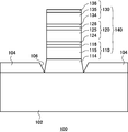
- FIG. 2 shows an example of a cross section of a semiconductor substrate 100.
- 2 shows an example of a cross section of a semiconductor substrate 100.
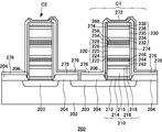
- An example of the cross section of the photoelectric conversion device 200 is shown.
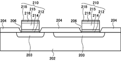
- the cross-sectional example in the manufacture process of the photoelectric conversion device 200 is shown.
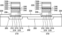
- the cross-sectional example in the manufacture process of the photoelectric conversion device 200 is shown.
- the cross-sectional example in the manufacture process of the photoelectric conversion device 200 is shown.
- the cross-sectional example in the manufacture process of the photoelectric conversion device 200 is shown.
- An example of the energy band of the light absorption structure in the semiconductor substrate 100 is shown.
- An example of the composition distribution of the first semiconductor in the semiconductor substrate 100 is shown.
- An example of the cross section of the photoelectric conversion device 1000 is shown.
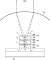
- the focal position of the condensing member which has chromatic aberration is shown.
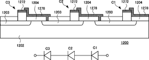
- An example of the cross section of the photoelectric conversion device 1200 is shown.
- An example of a cross section of a photoelectric conversion device 1300 is shown.
- FIG. 1A shows an example of a cross section of a semiconductor substrate 100 according to an embodiment.
- the semiconductor substrate 100 includes a base substrate 102, an inhibitor 104, and a light absorption structure 140.
- the light absorption structure 140 includes a first semiconductor 110 and a second semiconductor 120.
- the base substrate 102 is a substrate containing silicon.
- a substrate whose surface is silicon can be given.
- the base substrate 102 is a Si substrate or an SOI (silicon-on-insulator) substrate.
- the base substrate 102 is, for example, a Si substrate having a B doping amount of 2.0 ⁇ 10 19 cm ⁇ 3 .
- the inhibitor 104 is formed on the base substrate 102.
- an opening 106 that exposes the surface of the base substrate 102 is formed.
- Inhibitor 104 inhibits crystal growth. For example, when a semiconductor crystal is grown by an epitaxial growth method, the semiconductor crystal is selectively epitaxially grown in the opening 106 because the epitaxial growth of the semiconductor crystal is inhibited on the surface of the inhibitor 104.
- the thickness of the inhibitor 104 is preferably 0.01 ⁇ m or more and 5 ⁇ m or less, for example.
- the size of the opening 106 is preferably such that a semiconductor that selectively grows inside the opening 106 can be formed without dislocation.
- the inhibitor 104 is, for example, a silicon oxide layer, a silicon nitride layer, a silicon oxynitride layer, or the like, or a layer in which these are stacked.
- the inhibitor 104 is formed by, for example, a thermal oxidation method or a CVD method.
- the first semiconductor 110 includes a first conduction type first semiconductor 114, a low carrier concentration first semiconductor 115, and a second conduction type first semiconductor 116.
- the first conduction type first semiconductor 114 has a P-type or N-type conduction type.
- the second conductive type first semiconductor 116 is formed above the first conductive type first semiconductor 114.
- the second conductivity type first semiconductor 116 has a conductivity type different from that of the first conductivity type first semiconductor 114. For example, when the first conductive first semiconductor 114 has a P-type conductivity, the second conductive first semiconductor 116 has an N-type conductivity.
- the low carrier concentration first semiconductor 115 is formed between the first conductive type first semiconductor 114 and the second conductive type first semiconductor 116.
- the effective carrier concentration in the first semiconductor 115 having a low carrier concentration is lower than the effective carrier concentration in the first conductive type first semiconductor 114 and the second conductive type first semiconductor 116.
- the low carrier concentration first semiconductor 115 is an intrinsic semiconductor having the same composition as the first conductive type first semiconductor 114 and the second conductive type first semiconductor 116.
- the low carrier concentration first semiconductor 115 may be a space charge region formed between the first conductive type first semiconductor 114 and the second conductive type first semiconductor 116.
- the “space charge region” refers to a region formed in a semiconductor due to a spatial charge bias (build-in potential) at a semiconductor-semiconductor interface or a semiconductor-metal interface.
- the space charge region is formed by a semiconductor PN junction, a PIN junction, a Schottky junction between a metal and a semiconductor, a dielectric and a semiconductor junction, or the like.
- the low carrier concentration first semiconductor 115 generates electrons and holes when irradiated with light. Electrons generated in the first semiconductor 115 with a low carrier concentration move to the semiconductor having the N-type conductivity among the first conductivity-type first semiconductor 114 and the second conductivity-type first semiconductor 116. The holes generated in the low carrier concentration first semiconductor 115 move to the semiconductor having P-type conductivity. As a result, the first semiconductor 110 functions as a photoelectric conversion device that generates an electrical signal when irradiated with light.
- the first semiconductor 110 is formed in contact with the surface of the base substrate 102 exposed to the inside of the opening 106 of the inhibitor 104 or inside the opening 106 or inside the opening 106 and above the inhibitor 104.
- the semiconductor substrate 100 may include another semiconductor layer between the first semiconductor 110 and the base substrate 102.
- the semiconductor substrate 100 may include a seed crystal that provides a seed crystal plane suitable for crystal growth of the first semiconductor 110 between the first semiconductor 110 and the base substrate 102.
- the second semiconductor 120 includes a first conductive type second semiconductor 124, a low carrier concentration second semiconductor 125, and a second conductive type second semiconductor 126.
- the first conductive type second semiconductor 124 has a P type or an N type.
- the first conductive type second semiconductor 124 is lattice-matched or pseudo-lattice matched to the second conductive type first semiconductor 116.
- “pseudo-lattice matching” is not perfect lattice matching, but is in contact with each other within a range where the difference in lattice constant between two semiconductors in contact with each other is small and defects due to lattice mismatch are not remarkable.
- the stacked state of Ge and GaAs is a pseudo lattice matched state.
- the second conductive type second semiconductor 126 is formed above the first conductive type second semiconductor 124.
- the second conductivity type second semiconductor 126 has a conductivity type different from that of the first conductivity type second semiconductor 124.
- the first conductive type second semiconductor 124 has a P-type conductive type
- the second conductive type second semiconductor 126 has an N-type conductive type.
- the low carrier concentration second semiconductor 125 is formed between the first conductive type second semiconductor 124 and the second conductive type second semiconductor 126.
- the effective carrier concentration in the low carrier concentration second semiconductor 125 is lower than the effective carrier concentration in the first conduction type second semiconductor 124 and the second conduction type second semiconductor 126.
- the low carrier concentration second semiconductor 125 is an intrinsic semiconductor having the same composition as the first conductive type second semiconductor 124 and the second conductive type second semiconductor 126.
- the low carrier concentration second semiconductor 125 may be a space charge region formed between the first conductive type second semiconductor 124 and the second conductive type second semiconductor 126.
- the low carrier concentration second semiconductor 125 generates electrons and holes when irradiated with light. Electrons generated in the second semiconductor 125 with the low carrier concentration move to the semiconductor having the N-type conductivity among the first conductivity-type second semiconductor 124 and the second conductivity-type second semiconductor 126. The holes generated in the low carrier concentration second semiconductor 125 move to the semiconductor having P-type conductivity. As a result, the second semiconductor 120 functions as a photoelectric conversion device that generates an electrical signal when irradiated with light.
- the semiconductor substrate 100 may include another semiconductor layer between the first semiconductor 110 and the second semiconductor 120.
- the semiconductor substrate 100 includes a semiconductor layer that forms a tunnel junction between the first semiconductor 110 and the second semiconductor 120.
- the first semiconductor 110 and the second semiconductor 120 are, for example, compound semiconductors.
- the first semiconductor 110 is, for example, C x1 Si y1 Ge z1 Sn 1-x1-y1-z1 (0 ⁇ x1 ⁇ 1, 0 ⁇ y1 ⁇ 1, 0 ⁇ z1 ⁇ 1, and 0 ⁇ x1 + y1 + z1 ⁇ 1).
- the first semiconductor 110 is made of amorphous or polycrystalline C x1 Si y1 Ge z1 Sn 1-x1-y1-z1 (0 ⁇ x1 ⁇ 1, 0 ⁇ y1 ⁇ 1, 0 ⁇ z1 ⁇ 1, and 0 ⁇ x1 + y1 + z1 ⁇ 1).
- the first semiconductor 110 is Ge or SiGe.
- the first semiconductor 110 may further include a plurality of semiconductor layers composed of Ge and SiGe having different compositions.
- the second semiconductor 120 may be Al x2 In y2 Ga 1-x2-y2 As z2P w1 N 1-z2-w1 (0 ⁇ x2 ⁇ 1, 0 ⁇ y2 ⁇ 1, and 0 ⁇ x2 + y2 ⁇ 1, and 0 ⁇ z2 ⁇ 1, 0 ⁇ w1 ⁇ 1, and 0 ⁇ z2 + w1 ⁇ 1).
- the second semiconductor 120 is, for example, InGaAs.
- the second semiconductor 120 may include a plurality of semiconductor layers.
- the first semiconductor 110 and the second semiconductor 120 are formed by an epitaxial growth method as an example.
- epitaxial growth methods chemical vapor deposition (referred to as CVD method), metal organic chemical vapor deposition (referred to as MOCVD method), molecular beam epitaxy method (referred to as MBE method), and atomic layer growth method (referred to as ALD method). ) Etc.
- the inhibitor 104 is formed on the base substrate 102 by a thermal oxidation method, and the opening 106 reaching the surface of the base substrate 102 is formed in the inhibitor 104 by a photolithography method such as etching.
- the first semiconductor 110 can be formed by sequentially growing the first conductive type first semiconductor 114 and the second conductive type first semiconductor 116 inside the opening 106 by CVD. By selectively growing the first semiconductor 110 inside the opening 106, generation of lattice defects due to the difference in lattice constant between the first semiconductor 110 and the base substrate 102 can be suppressed. As a result, the crystallinity of the first semiconductor 110 is increased, so that the photoelectric conversion efficiency in the first semiconductor 110 can be increased.
- the first semiconductor 110 is preferably heated after crystal growth.
- lattice defects such as dislocation may occur due to a difference in lattice constant between the base substrate 102 and the first semiconductor 110.
- lattice defects move inside the first semiconductor 110.
- the lattice defect moves inside the first semiconductor 110 and is captured and eliminated by a gettering sink or the like in the interface or side wall of the first semiconductor 110 or in the first semiconductor 110.
- the size of the opening 106 of the inhibitor 104 By making the size of the opening 106 of the inhibitor 104 equal to or smaller than a certain size, the size of the first semiconductor 110 selectively grown inside the opening 106 can be limited. If the size of the opening 106 is such that lattice defects can move to the surface of the first semiconductor 110 by heating, the lattice defects inside the first semiconductor 110 are eliminated by heating, and the first semiconductor having extremely high crystallinity. 110 can be manufactured.
- Bottom area of the opening 106 is preferably not 1 mm 2 or less, more preferably 25 [mu] m 2 or more 2500 [mu] m 2 or less, even more preferably at 100 [mu] m 2 or more 1600 .mu.m 2 or less, particularly preferably is 400 [mu] m 2 or more 900 .mu.m 2 or less . If the bottom area of the opening is smaller than 25 ⁇ m 2 , the area is small in producing a photoelectric device, which is not preferable. By increasing the crystallinity of the first semiconductor 110, the photoelectric conversion efficiency of the first semiconductor 110 is further increased.
- the second semiconductor 120 is formed inside the opening 106 or inside the opening 106 and above the inhibitor 104, for example.
- the second semiconductor 120 grows using the first semiconductor 110 as a seed crystal. Since the first semiconductor 110 has high crystallinity when the first semiconductor 110 grows inside the opening 106, the second semiconductor 120 lattice-matched or pseudo-lattice-matched to the first semiconductor 110 also has high crystallinity. . As a result, the photoelectric conversion efficiency of the second semiconductor 120 can be increased.
- the first semiconductor 110 is made of a material having a first forbidden bandwidth.
- the second semiconductor 120 is made of a material having a second forbidden band width larger than the first forbidden band width.
- the photoelectric device absorbs light having energy corresponding to the forbidden bandwidth and converts it into electric power.
- the first semiconductor 110 absorbs light having energy corresponding to the first forbidden band and performs photoelectric conversion.
- the second semiconductor 120 has a second forbidden band wider than the first semiconductor 110, the second semiconductor 120 absorbs light having a wavelength shorter than the wavelength of light absorbed by the first semiconductor 110 and performs photoelectric conversion. Since the semiconductor substrate 100 has the above-described two-layer tandem structure, the semiconductor substrate 100 can effectively absorb light over a wide wavelength range, so that the photoelectric conversion efficiency can be increased.
- FIG. 1B shows another example of a cross section of the semiconductor substrate 100.
- the semiconductor substrate 100 further includes a third semiconductor 130 with respect to the semiconductor substrate 100 shown in FIG. 1A.
- the third semiconductor 130 is formed above the second semiconductor 120 in lattice matching or pseudo-lattice matching with the second semiconductor 120.
- the third semiconductor 130 includes a first conductive type third semiconductor 134, a low carrier concentration third semiconductor 135, and a second conductive type third semiconductor 136.
- the first conductive type third semiconductor 134 has a P-type or N-type conductivity type.
- the first conductive type third semiconductor 134 is lattice-matched or pseudo-lattice matched to the second conductive type second semiconductor 126.
- the second conductive type third semiconductor 136 is formed above the first conductive type third semiconductor 134.
- the second conductivity type third semiconductor 136 has a conductivity type different from that of the first conductivity type third semiconductor 134.
- the low carrier concentration third semiconductor 135 is formed between the first conductive third semiconductor 134 and the second conductive third semiconductor 136.
- the effective carrier concentration in the low carrier concentration third semiconductor 135 is lower than the effective carrier concentration in the first conduction type third semiconductor 134 and the second conduction type third semiconductor 136.
- the low carrier concentration third semiconductor 135 is an intrinsic semiconductor having the same composition as the first conductive type third semiconductor 134 and the second conductive type third semiconductor 136.
- the low carrier concentration third semiconductor 135 may be a space charge region formed between the first conductive third semiconductor 134 and the second conductive third semiconductor 136.
- the third semiconductor is, for example, Al x3 In y3 Ga 1-x3-y3 As z3 P 1-z3 (0 ⁇ x3 ⁇ 1, 0 ⁇ y3 ⁇ 1, 0 ⁇ z3 ⁇ 1, and 0 ⁇ x3 + y3 ⁇ 1).
- the third semiconductor 130 may include a material having a third forbidden band width larger than the second forbidden band width of the second semiconductor 120.
- the first semiconductor 110, the second semiconductor 120, and the third semiconductor are formed in the opening 106, for example. Part of the first semiconductor 110, the second semiconductor 120, and the third semiconductor 130 may be formed above the inhibitor 104. Since the semiconductor substrate 100 has a three-layer tandem structure including the first semiconductor 110, the second semiconductor 120, and the third semiconductor 130, the semiconductor substrate 100 has a wider wavelength range than the semiconductor substrate 100 illustrated in FIG. 1A. Since light can be effectively absorbed, photoelectric conversion efficiency can be increased.
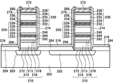
- FIG. 2 shows an example of a cross section of a photoelectric conversion device 200 according to another embodiment.
- the photoelectric conversion device 200 includes a base substrate 202, a well 203, an inhibitor 204, a first semiconductor 210, a second semiconductor 220, a third semiconductor 230, a buffer layer 242, a semiconductor 244, a semiconductor 246, a semiconductor 254, a semiconductor 256, and a contact layer. 268, a transparent electrode 272, a passivation layer 274, an insulating film 276, and a wiring 278.
- the inhibitor 204 has a plurality of openings 206.
- the photoelectric conversion device 200 includes a light absorption structure C1 and a light absorption structure C2 formed in the plurality of openings 206.
- the photoelectric conversion device 200 may include more light absorption structures.
- the light absorption structure C1 and the light absorption structure C2 have the same configuration as an example. The following description of the light absorption structure C1 can be applied to the light absorption structure C2.
- the base substrate 202 corresponds to the base substrate 102 in FIG. 1A and has the same configuration as the base substrate 102.
- the inhibitor 204 corresponds to the inhibitor 104 and has the same configuration as the inhibitor 104.
- the first semiconductor 210 includes a BSF (Back Surface Field) 212, a first conduction type first semiconductor 214, a low carrier concentration first semiconductor 215, a second conduction type first semiconductor 216, and a window 218.
- the first semiconductor 210 is, for example, a group IV compound semiconductor.
- the first semiconductor 210 may be C x1 Si y1 Ge z1 Sn 1-x1-y1-z1 (0 ⁇ x1 ⁇ 1, 0 ⁇ y1 ⁇ 1, 0 ⁇ z1 ⁇ 1, and 0 ⁇ x1 + y1 + z1 ⁇ 1). is there.
- the first semiconductor 210 is, for example, Ge, SiGe, or CSiGe.
- the first semiconductor 210 may have a double heterojunction.
- the first semiconductor 210 may include a material having a first forbidden band width.
- the first conductive type first semiconductor 214 corresponds to the first conductive type first semiconductor 114 in FIG. 1A.
- the second conductive type first semiconductor 216 corresponds to the second conductive type first semiconductor 116.
- the light absorption structure C ⁇ b> 1 is less effective between the first conductive type first semiconductor 214 and the second conductive type first semiconductor 216 than the first conductive type first semiconductor 214 and the second conductive type first semiconductor 216.
- a low carrier concentration first semiconductor 215 having a carrier concentration is included.
- the first conductive type first semiconductor 214 is P-type Ge having a thickness of 0.5 ⁇ m or more and 50.0 ⁇ m or less.
- the first conductive type first semiconductor 214 is 2.0 ⁇ m P-type Ge.
- the low carrier concentration first semiconductor 215 is P-type Ge having a thickness of 0.3 ⁇ m or more and 3.0 ⁇ m or less and a carrier concentration of 1.0 ⁇ 10 16 cm ⁇ 3 or more and 1.0 ⁇ 10 18 cm ⁇ 3 or less.
- P-type Ge having a B doping amount of 1.0 ⁇ 10 16 cm ⁇ 3 or more and 1.0 ⁇ 10 18 cm ⁇ 3 or less can be exemplified.
- the low carrier concentration first semiconductor 215 is 1.0 ⁇ m P-type Ge.
- the second conductive type first semiconductor 216 N having a thickness of 0.02 ⁇ m to 5.0 ⁇ m and a P (phosphorus) doping amount of 1 ⁇ 10 18 cm ⁇ 3 to 5 ⁇ 10 20 cm ⁇ 3.
- the type Ge can be exemplified.
- the second conductive type first semiconductor 216 is N-type Ge having a thickness of 0.05 ⁇ m and a P (phosphorus) doping amount of 2.0 ⁇ 10 18 cm ⁇ 3 .
- the first semiconductor 210 including the first conductive type first semiconductor 214 and the second conductive type first semiconductor 216 has a first forbidden band width of, for example, 0.66 eV.
- the BSF 212 is an example of a recombination inhibitor that suppresses recombination of charges.
- BSF is an abbreviation for Back Surface Field.
- recombination means that excited electrons and excited holes are combined and disappear.
- the BSF 212 may have a larger forbidden band width than the first conductive type first semiconductor 214 and the second conductive type first semiconductor 216.
- the BSF 212 is formed above the base substrate 202.
- the BSF 212 is a semiconductor that lattice matches or pseudo lattice matches with the base substrate 202.
- Examples of the BSF 212 include P-type SiGe having a thickness of 0.01 ⁇ m to 0.5 ⁇ m and a Ga doping amount of 5 ⁇ 10 18 cm ⁇ 3 or more and 5 ⁇ 10 20 cm ⁇ 3 or less.
- the BSF 212 is P-type Si 0.1 Ge 0.9 having a thickness of 0.02 ⁇ m and a Ga doping amount of 2.0 ⁇ 10 19 cm ⁇ 3 .
- the window 218 is an example of a recombination suppressor that suppresses charge recombination.
- the window 218 may have a larger forbidden band width than the first conductive type first semiconductor 214 and the second conductive type first semiconductor 216.
- the window 218 is formed on the second conductive type first semiconductor 216.
- the window 218 is a semiconductor that is lattice-matched or pseudo-lattice-matched to the second conductivity type first semiconductor 216.
- Examples of the window 218 include N-type GaInP having a thickness of 0.01 ⁇ m to 0.3 ⁇ m and a Si doping amount of 1 ⁇ 10 18 cm ⁇ 3 or more and 4 ⁇ 10 19 cm ⁇ 3 or less.
- the window 218 is N-type Ga 0.5 In 0.5 P having a thickness of 0.02 ⁇ m and an Si doping amount of 5.0 ⁇ 10 18 cm ⁇ 3 .
- Each semiconductor layer included in the first semiconductor 210 is formed by, for example, an epitaxial growth method.
- the epitaxial growth method include a CVD method, an MOCVD method, an MBE method, and an ALD method.
- the inhibitor 204 having a plurality of openings 206 exposing the surface of the base substrate 202 is formed on the base substrate 202 by the above-described method.
- the BSF 212, the first conductive type first semiconductor 214, the low carrier concentration first semiconductor 215, the second conductive type first semiconductor 216, and the window 218 are sequentially grown selectively in the opening 206 by the MOCVD method.
- the first semiconductor 210 can be formed.
- the first semiconductor 210 is formed in the opening 206, for example, in contact with the surface of the base substrate 202 exposed in the opening 206 of the inhibitor 204. A part of the first semiconductor 210 may protrude from the opening 206 and be formed above the inhibitor 204.
- the buffer layer 242 is formed above the window 218, for example.
- the buffer layer 242 is a semiconductor that lattice matches or pseudo lattice matches with the window 218, for example.
- the buffer layer 242 may be a semiconductor layer that can reduce adverse effects between the semiconductor layers above and below it.
- the buffer layer 242 is formed by, for example, an epitaxial growth method. Examples of the epitaxial growth method include a CVD method, an MOCVD method, an MBE method, and an ALD method.
- the buffer layer 242 examples include N-type GaAs having a thickness of 0.01 ⁇ m to 0.5 ⁇ m and a Si doping amount of 2.0 ⁇ 10 18 cm ⁇ 3 to 2.0 ⁇ 10 19 cm ⁇ 3 .
- the buffer layer 242 is N-type GaAs having a thickness of 0.1 ⁇ m and a Si doping amount of 3.0 ⁇ 10 18 cm ⁇ 3 .
- the semiconductor 244 and the semiconductor 246 are a P-type semiconductor doped with a high concentration of P-type impurities or an N-type semiconductor doped with a high concentration of N-type impurities.
- the semiconductor 244 and the semiconductor 246 are semiconductors having different conductivity types.
- the semiconductor 244 and the semiconductor 246 may be tunnel-junctioned.
- the semiconductor 244 is an N-type semiconductor doped with a high concentration of N-type impurities and the semiconductor 246 is a P-type semiconductor doped with a high concentration of P-type impurities
- the semiconductor 244 and the semiconductor 246 A tunnel junction is formed at the interface.
- the light absorption structure C1 has the tunnel junction, electrons or holes generated between the first semiconductor 210 and the second semiconductor 220 by photoelectric conversion are generated between the first semiconductor 210 and the second semiconductor 220. Flows smoothly. As a result, the light absorbing structure C1 can output current efficiently.
- Examples of the semiconductor 244 include N-type GaAs having a thickness of 0.01 ⁇ m to 0.2 ⁇ m and a Si doping amount of 3.0 ⁇ 10 18 cm ⁇ 3 to 2.0 ⁇ 10 19 cm ⁇ 3 .
- the semiconductor 244 is, for example, N-type GaAs having a thickness of 0.015 ⁇ m and an Si doping amount of 1.0 ⁇ 10 19 cm ⁇ 3 or more.
- An example of the semiconductor 246 is P-type GaAs having a thickness of 0.01 ⁇ m to 0.2 ⁇ m and a C doping amount of 2.0 ⁇ 10 19 cm ⁇ 3 to 1.0 ⁇ 10 21 cm ⁇ 3.
- the semiconductor 246 is, for example, P-type GaAs having a thickness of 0.015 ⁇ m and a C doping amount of 1.0 ⁇ 10 20 cm ⁇ 3 or more.
- the semiconductor 244 and the semiconductor 246 are formed above the buffer layer 242.
- the semiconductor 244 and the semiconductor 246 are semiconductors that lattice match or pseudo lattice match with the buffer layer 242.
- the semiconductor 244 and the semiconductor 246 can be formed by an epitaxial growth method. Examples of the epitaxial growth method include a CVD method, an MOCVD method, an MBE method, and an ALD method.
- the semiconductor 244 and the semiconductor 246 can be sequentially selectively grown above the buffer layer 242 by MOCVD.
- the second semiconductor 220 includes a BSF 222, a first conductive type second semiconductor 224, a second conductive type second semiconductor 226, and a window 228.
- the second semiconductor 220 is, for example, a compound semiconductor.
- the second semiconductor 220 is, for example, Al x2 In y2 Ga 1-x2-y2 As z2P w1 N 1-z2-w1 (0 ⁇ x2 ⁇ 1, 0 ⁇ y2 ⁇ 1, and 0 ⁇ x2 + y2 ⁇ 1, and 0 ⁇ z2 ⁇ 1, 0 ⁇ w1 ⁇ 1, and 0 ⁇ z2 + w1 ⁇ 1).
- the second semiconductor 220 may be InGaAs.
- the second semiconductor 220 may have a double heterojunction.
- the second semiconductor 220 may include a material having a second forbidden band width larger than the first forbidden band width of the first semiconductor 210.
- the first conductive type second semiconductor 224 corresponds to the first conductive type second semiconductor 124 in FIG. 1A.
- the second conductive type second semiconductor 226 corresponds to the second conductive type second semiconductor 126.
- the light absorption structure C ⁇ b> 1 is less effective between the first conductive type second semiconductor 224 and the second conductive type second semiconductor 226 than the first conductive type second semiconductor 224 and the second conductive type second semiconductor 226.
- a low carrier concentration second semiconductor 225 having a carrier concentration is included.
- the first conductive type second semiconductor 224 is a P-type having a thickness of 0.3 ⁇ m to 3.0 ⁇ m and a Zn doping amount of 1.0 ⁇ 10 17 cm ⁇ 3 to 1.0 ⁇ 10 20 cm ⁇ 3. InGaAs can be exemplified.
- the first conductive type second semiconductor 224 is, for example, P-type In 0.01 Ga 0.99 As having a thickness of 0.05 ⁇ m and a Zn doping amount of 1.0 ⁇ 10 19 cm ⁇ 3 .
- P-type InGaAs having a thickness of 0.3 ⁇ m to 3.0 ⁇ m and a carrier concentration of 1.0 ⁇ 10 16 cm ⁇ 3 to 1.0 ⁇ 10 18 cm ⁇ 3 is used.
- P-type InGaAs having a Zn doping amount of 1.0 ⁇ 10 16 cm ⁇ 3 or more and 1.0 ⁇ 10 18 cm ⁇ 3 or less can be exemplified.
- P-type In0.01Ga0.99As having a thickness of 1.0 ⁇ m, a carrier concentration of 1.0 ⁇ 10 17 cm ⁇ 3 , and a Zn doping amount of 1.0 ⁇ 10 17 cm ⁇ 3 can be given. .
- the second conductive type second semiconductor 226 is an N-type having a thickness of 0.01 ⁇ m to 1 ⁇ m and an Si doping amount of 5.0 ⁇ 10 17 cm ⁇ 3 to 6.0 ⁇ 10 18 cm ⁇ 3. InGaAs can be exemplified.
- the second conductive type second semiconductor 226 is, for example, N-type In 0.01 Ga 0.99 As having a thickness of 0.05 ⁇ m and an Si doping amount of 2.0 ⁇ 10 18 cm ⁇ 3 .
- the second semiconductor 220 including the first conductive type second semiconductor 224 and the second conductive type second semiconductor 226 has a second forbidden band width of, for example, 1.39 eV.
- the BSF 222 is an example of a recombination suppressor that suppresses charge recombination.
- the BSF 222 may have a larger forbidden band width than the first conductive type second semiconductor 224 and the second conductive type second semiconductor 226.
- the BSF 222 may be formed above the semiconductor 246.
- the BSF 222 is a semiconductor that lattice matches or pseudo-lattice matches with the semiconductor 246.
- Examples of the BSF 222 include P-type GaInP having a thickness of 0.01 ⁇ m to 1 ⁇ m and a Zn doping amount of 1.0 ⁇ 10 18 cm ⁇ 3 to 5.0 ⁇ 10 19 cm ⁇ 3 .
- the BSF 222 is, for example, P-type Ga 0.5 In 0.5 P having a thickness of 0.02 ⁇ m and a Zn doping amount of 2.0 ⁇ 10 19 cm ⁇ 3 .
- the window 228 is an example of a recombination suppressor that suppresses charge recombination.
- the window 228 may have a larger forbidden band width than the first conductive type second semiconductor 224 and the second conductive type second semiconductor 226.
- the window 228 is formed above the second conductive type second semiconductor 226, for example.
- the window 228 is a semiconductor that is lattice-matched or pseudo-lattice-matched to the second conductivity type second semiconductor 226.
- Examples of the window 228 include N-type GaInP having a thickness of 0.01 ⁇ m to 1 ⁇ m and a Si doping amount of 1.0 ⁇ 10 18 cm ⁇ 3 to 1.0 ⁇ 10 19 cm ⁇ 3 .
- the window 228 is N-type Ga 0.5 In 0.5 P having a thickness of 0.02 ⁇ m and an Si doping amount of 5.0 ⁇ 10 18 cm ⁇ 3 .
- Each semiconductor layer included in the second semiconductor 220 is formed by, for example, an epitaxial growth method.
- the epitaxial growth method include a CVD method, an MOCVD method, an MBE method, and an ALD method.
- the BSF 222, the first conductive type second semiconductor 224, the low carrier concentration second semiconductor 225, the second conductive type second semiconductor 226, and the window 228 are sequentially grown on the semiconductor 246 by MOCVD.
- the second semiconductor 220 can be formed.
- the second semiconductor 220 may be formed inside the opening 206 of the inhibitor 204, or a part of the second semiconductor 220 may be formed on the inhibitor 204 protruding from the opening 206.
- the semiconductor 254 and the semiconductor 256 are a P-type semiconductor doped with a high concentration of P-type impurities or an N-type semiconductor doped with a high concentration of N-type impurities.
- the semiconductor 254 and the semiconductor 256 are semiconductors having different conductivity types.
- the semiconductor 254 and the semiconductor 256 may be tunnel-junctioned.
- the semiconductor 254 and the semiconductor 256 A tunnel junction is formed at the interface.
- the light absorption structure C1 has the tunnel junction, electrons or holes formed in the second semiconductor 220 and the third semiconductor 230 by photoelectric conversion can smoothly flow between the second semiconductor 220 and the third semiconductor 230. Flowing. As a result, the light absorbing structure C1 can output current efficiently.
- An example of the semiconductor 254 is N-type GaAs having a thickness of 0.01 ⁇ m or more and 0.2 ⁇ m or less and an Si doping amount of 3.0 ⁇ 10 18 cm ⁇ 3 or more and 2.0 ⁇ 10 19 cm ⁇ 3 or less.
- the semiconductor 254 is, for example, N-type GaAs having a thickness of 0.015 ⁇ m and an Si doping amount of 1.0 ⁇ 10 19 cm ⁇ 3 or more.
- As the semiconductor 256 P-type GaAs having a thickness of 0.01 ⁇ m or more and 0.2 ⁇ m or less and a C doping amount of 2.0 ⁇ 10 19 cm ⁇ 3 or more and 1.0 ⁇ 10 21 cm ⁇ 3 or less can be exemplified. .
- the semiconductor 256 is, for example, P-type GaAs having a thickness of 0.015 ⁇ m and a C doping amount of 1.0 ⁇ 10 20 cm ⁇ 3 or more.
- the semiconductor 254 and the semiconductor 256 may be formed above the window 228.
- the semiconductor 254 and the semiconductor 256 are semiconductors that lattice-match or pseudo-lattice match with the window 228.
- the semiconductor 254 and the semiconductor 256 are formed by, for example, an epitaxial growth method. Examples of the epitaxial growth method include a CVD method, an MOCVD method, an MBE method, and an ALD method.
- the semiconductor 254 and the semiconductor 256 can be selectively grown sequentially over the window 228 by MOCVD.
- the third semiconductor 230 includes a BSF 232, a first conduction type third semiconductor 234, a low carrier concentration third semiconductor 235, a second conduction type third semiconductor 236, and a window 238.
- the third semiconductor 230 is, for example, a compound semiconductor.
- the third semiconductor 230 is, for example, Al x3 In y3 Ga 1-x3-y3 As z3 P 1-z3 (0 ⁇ x3 ⁇ 1, 0 ⁇ y3 ⁇ 1, 0 ⁇ z3 ⁇ 1, and 0 ⁇ x3 + y3 ⁇ 1). is there.
- the third semiconductor 230 may be GaInP.
- the third semiconductor may have a third space charge region.
- the third semiconductor 230 may have a double heterojunction.
- the third semiconductor may include a material having a third forbidden band width larger than the second forbidden band width.
- the BSF 232 is an example of a recombination suppressor that suppresses charge recombination.
- the BSF 232 has a larger forbidden band width than the first conductive type third semiconductor 234 and the second conductive type third semiconductor 236.
- the BSF 232 may be formed on the semiconductor 256.
- the BSF 232 is a semiconductor that lattice matches or pseudo-lattice matches with the semiconductor 256.
- Examples of the BSF 232 include P-type AlGaInP having a thickness of 0.01 ⁇ m to 1 ⁇ m and a Zn doping amount of 1.0 ⁇ 10 18 cm ⁇ 3 to 5.0 ⁇ 10 19 cm ⁇ 3 .
- the BSF 232 is, for example, P-type Al 0.1 Ga 0.4 In 0.5 P having a thickness of 0.02 ⁇ m and a Zn doping amount of 2.0 ⁇ 10 19 cm ⁇ 3 .
- the first conduction type third semiconductor 234 has a P-type or N-type conduction type.
- the second conductivity type third semiconductor 236 has a conductivity type different from that of the first conductivity type third semiconductor 234.
- the first conductive type third semiconductor 234 and the second conductive type second semiconductor 234 are used.
- a space charge region is formed in the third semiconductor 235 having a low carrier concentration with the third semiconductor 236.
- the third semiconductor 230 generates electrons and holes when light enters the space charge region.
- Electrons generated in the third semiconductor 230 move to the N-type semiconductor side of the first conduction type third semiconductor 234 and the second conduction type third semiconductor 236, and holes move to the P-type semiconductor side.
- the third semiconductor 230 functions as a photoelectric conversion device.
- the first conductive type third semiconductor 234 is a P-type having a thickness of 0.3 ⁇ m or more and 3.0 ⁇ m or less and a Zn doping amount of 1.0 ⁇ 10 17 cm ⁇ 3 or more and 1.0 ⁇ 10 20 cm ⁇ 3 or less.
- GaInP can be exemplified.
- the first conductive type third semiconductor 234 is P-type Ga 0.5 In 0.5 P having a thickness of 0.05 ⁇ m and a Zn doping amount of 1.0 ⁇ 10 19 cm ⁇ 3 .
- the third semiconductor 235 having a low carrier concentration P-type GaInP having a thickness of 0.3 ⁇ m to 3.0 ⁇ m and a carrier concentration of 1.0 ⁇ 10 16 cm ⁇ 3 to 1.0 ⁇ 10 18 cm ⁇ 3 is used.
- P-type GaInP having a Zn doping amount of 1.0 ⁇ 10 16 cm ⁇ 3 or more and 1.0 ⁇ 10 18 cm ⁇ 3 or less can be exemplified.
- the low carrier concentration third semiconductor 235 has a thickness of 1.0 ⁇ m, a carrier concentration of 1.0 ⁇ 10 17 cm ⁇ 3 , and a Zn doping amount of 1.0 ⁇ 10 17 cm ⁇ 3 .
- the second conductive type third semiconductor 236 an N type having a thickness of 0.01 ⁇ m to 1 ⁇ m and an Si doping amount of 5.0 ⁇ 10 17 cm ⁇ 3 to 6.0 ⁇ 10 18 cm ⁇ 3.
- GaInP can be exemplified.
- the second conductive third semiconductor 236 is N-type Ga 0.5 In 0.5 P having a thickness of 0.05 ⁇ m and an Si doping amount of 2.0 ⁇ 10 18 cm ⁇ 3 .
- the third semiconductor 230 has a third forbidden band width of 1.80 eV, for example.
- the window 238 is an example of a recombination suppressor that suppresses charge recombination.
- the window 238 has a larger forbidden band width than the first conductive type third semiconductor 234 and the second conductive type third semiconductor 236.
- the window 238 is formed above the second conductive type third semiconductor 236.
- the window 238 is a semiconductor that lattice-matches or pseudo-lattice-matches with the second conductivity type third semiconductor 236.
- Examples of the window 238 include N-type AlGaInP having a thickness of 0.01 ⁇ m to 1 ⁇ m and a Si doping amount of 1.0 ⁇ 10 18 cm ⁇ 3 to 1.0 ⁇ 10 19 cm ⁇ 3 .
- the window 238 is N-type Al 0.1 Ga 0.4 In 0.5 P having a thickness of 0.02 ⁇ m and an Si doping amount of 5.0 ⁇ 10 18 cm ⁇ 3 .
- Each semiconductor layer included in the third semiconductor 230 is formed by, for example, an epitaxial growth method.
- the epitaxial growth method include a CVD method, an MOCVD method, an MBE method, and an ALD method.
- the BSF 232, the first conductive type third semiconductor 234, the low carrier concentration third semiconductor 235, the second conductive type third semiconductor 236, and the window 238 are sequentially grown on the semiconductor 256 by the MOCVD method.
- Three semiconductors 230 can be formed.
- the third semiconductor 230 is formed inside the opening 206 of the inhibitor 204, for example. A part of the third semiconductor 230 may protrude from the opening 206 and be formed on the inhibitor 204.
- the contact layer 268 is a semiconductor provided in order to ensure electrical conductivity between the transparent electrode 272 and the third semiconductor 230 formed thereon.
- Contact layer 268 may have the same conductivity type as window 238.
- the contact layer 268 is formed on the window 238.
- the contact layer 268 is a semiconductor that lattice matches or pseudo lattice matches with the window 238. Examples of the contact layer 268 include N-type GaAs having a thickness of 0.01 ⁇ m or more and 0.05 ⁇ m or less and an Si doping amount of 3.0 ⁇ 10 18 cm ⁇ 3 or more and 2.0 ⁇ 10 19 cm ⁇ 3 or less.
- the contact layer 268 is N-type GaAs having a thickness of 0.10 ⁇ m and a Si doping amount of 6.0 ⁇ 10 18 cm ⁇ 3 .
- it is N-type GaAs having a thickness of 0.10 ⁇ m and a Te doping amount of 2.0 ⁇ 10 19 cm ⁇ 3 .
- the contact layer 268 is formed by, for example, an epitaxial growth method.
- the epitaxial growth method include a CVD method, an MOCVD method, an MBE method, and an ALD method.
- the contact layer 268 can be selectively grown on the window 238 by MOCVD.
- the passivation layer 274 is formed on the side wall of the light absorption structure C1, and suppresses charge recombination on the side wall.
- a material of the passivation layer 274 InGaP can be exemplified.
- Examples of a method for forming the passivation layer 274 include a CVD method, an MOCVD method, an MBE method, and an ALD method.
- the insulating film 276 electrically isolates each light absorption structure.
- Examples of the material of the insulating film 276 include Al 2 O 3 , SiO 2 , Si 3 N 4 , ZrO 2, and the like.
- the insulating film 276 can be formed using a plasma CVD method, an ion plating method, a sputtering method, a CVD method, an MOCVD method, or the like.
- the transparent electrode 272 is formed in contact with the contact layer 268, for example.
- the transparent electrode 272 outputs electric power from the light absorption structure C1 to the outside.
- the transparent electrode 272 includes a material that has conductivity and does not block light incident on the light absorption structure C1. Examples of the material of the transparent electrode 272 include ITO (Indium Tin Oxide), ZnO, and TiO 2 . Examples of a method for forming the transparent electrode 272 include a sputtering method.
- the well 203 is formed in silicon included in the base substrate 202 and is electrically coupled to the first semiconductor of the light absorption structure C1.
- the well 203 is electrically isolated from the silicon bulk region.
- a PN junction is formed between the well 203 and the silicon, so that the well 203 and the silicon are electrically separated.
- the electric power generated by the light absorbing structure C1 can be taken out as an electromotive force between the well 203 and the transparent electrode 272.
- the well 203 is formed by an ion implantation method or a thermal diffusion method.
- the well 203 can be formed by ion implantation after forming a mask having an opening at a position where the well 203 is to be formed on the base substrate 202 by a photolithography method such as etching.
- the P-type well 203 can be formed by implanting or diffusing B into the N-type Si base substrate 202.
- the wiring 278 is connected to the transparent electrode 272 and outputs the electric power extracted from the light absorption structure C1 through the transparent electrode 272 to an external circuit.
- the wiring 278 connects the transparent electrode 272 of the light absorption structure C2 to the well 203 of the light absorption structure C1, thereby connecting the two light absorption structures in series.
- the material of the wiring 278 include Cu, Ag, and Al.
- the method for forming the wiring 278 include a CVD method, a vacuum deposition method, and a sputtering method.
- the photoelectric conversion device 200 has a three-layer tandem structure including a first semiconductor 210, a second semiconductor 220, and a third semiconductor 230. Since the photoelectric conversion device 200 has a three-layer tandem structure, the photoelectric conversion device 200 can effectively absorb light over a wide wavelength range, so that the photoelectric conversion efficiency can be increased.
- the method of manufacturing the photoelectric conversion device 200 includes a step of forming a well, a step of forming an inhibitor, a step of forming a first semiconductor, a step of heating the first semiconductor, a step of forming a second semiconductor, and a step of forming a third semiconductor. Forming, passivating, and connecting the light absorbing structures in series or in parallel.
- the well 203 is formed on the base substrate 202.
- a mask having an opening at a position where the well 203 is to be formed is formed on the base substrate 202 by a photolithography method such as etching.
- B ions are implanted to form the well 203.
- the inhibitor 204 having the opening 206 exposing the surface of the base substrate 202 is formed on the base substrate 202.
- the inhibitor 204 is formed by first forming a silicon oxide film on the entire surface of the base substrate 202 by, for example, a thermal oxidation method.
- a photolithography method such as etching
- the first semiconductor 210 is formed inside the opening 206 by selective epitaxial growth. For example, using MOCVD, P-type SiGe BSF 212, P-type Ge first conductive first semiconductor 214, low carrier concentration first semiconductor 215, N-type Ge second conductive first semiconductor 216, and N A first semiconductor 210 having a type GaInP window 218 is epitaxially grown.
- the Si base substrate 202 on which the inhibitor 204 having the opening 206 is formed is placed on a heating table of a reduced pressure barrel type MOCVD furnace.
- heating of the base substrate 202 is started.
- the substrate temperature during crystal growth is 500 ° C. to 800 ° C.
- a Si raw material is introduced into the furnace, and then a Ge raw material is introduced to epitaxially grow a P-type SiGe BSF 212.
- Examples of the Si raw material include chlorosilane, dichlorosilane, trichlorosilane, tetrachlorosilane, silane, and disilane.
- Examples of the Ge raw material include germane and tetramethylgermanium ((CH 3 ) 4 Ge).
- the acceptor impurity may be Ga, and trimethylgallium (TMG) may be used as the P-type dopant.
- B and Al can be used as other acceptor impurities.
- Trimethylboron (TMB) and trimethylaluminum (TMA) can be used as the dopant.
- the first conductive type first semiconductor 214 of P-type Ge, the second conductive type first semiconductor 216 of N-type Ge, and the window 218 of N-type GaInP may be epitaxially grown on the BSF 212 sequentially.
- An example of the In source material is trimethylindium (TMI).
- An example of P raw material is phosphine (PH 3 ). Further, P may be used as a donor impurity, and phosphine may be used as an N-type dopant. Further, As can be used as another donor impurity. Arsine (AsH 3 ) can be used as a dopant.
- the reactor pressure is 0.1 atm
- the growth temperature is 650 ° C.
- the growth rate is 1 to 3 ⁇ m / hr.
- High purity hydrogen can be used as a carrier gas for the raw material.
- Each semiconductor formation method described later can also be epitaxially grown by adjusting parameters such as source gas, furnace pressure, growth temperature, and growth time using the same MOCVD method.
- the first semiconductor 210 may be heated in a plurality of stages. For example, after performing high temperature annealing at a temperature that does not reach the melting point of the first semiconductor 210, low temperature annealing is performed at a temperature lower than the temperature of the high temperature annealing. Such two-stage annealing may be repeated a plurality of times.
- the first semiconductor 210 is heated.
- the first semiconductor 210 may be heated after a part of the semiconductor included in the first semiconductor is formed.
- the first semiconductor 210 may be heated after only the P-type SiGe BSF 212 is formed.
- the temperature and time of the high temperature annealing are, for example, 850 to 900 ° C. and 2 to 10 minutes.
- the temperature and time of the low-temperature annealing are, for example, 650 to 780 ° C. and 2 to 10 minutes.
- Such two-step annealing may be repeated, for example, 10 times.
- the buffer layer 242, the semiconductor 244, the semiconductor 246, and the second semiconductor 220 are sequentially formed by an epitaxial growth method.
- an N-type GaAs buffer layer 242 is epitaxially grown in contact with the window 218.
- an N-type GaAs semiconductor 244, a P-type GaAs semiconductor 246, a P-type GaInP BSF 222, a P-type InGaAs first conductive second semiconductor 224, and a low carrier concentration second semiconductor 225 are sequentially disposed above the buffer layer 242.
- the second conductive second semiconductor 226 of N-type InGaAs and the window 228 of N-type GaInP may be epitaxially grown.
- An example of an As raw material is arsine (AsH 3 ).
- acceptor impurities include C and Zn.
- donor impurities further include Si, Se, Ge, Sn, Te, and S.
- the semiconductor 254, the semiconductor 256, the third semiconductor, and the contact layer 268 are sequentially formed by the epitaxial growth method.
- the semiconductor 254, the semiconductor 256, the third semiconductor, and the contact layer 268 are sequentially formed by the epitaxial growth method.
- an N-type GaAs semiconductor 254 is epitaxially grown in contact with the window 228.
- a P-type GaAs semiconductor 256, a P-type AlGaInP BSF 232, a P-type GaInP first conductive type third semiconductor 234, a low carrier concentration third semiconductor 235, and an N-type GaInP second conductive are epitaxially grown.
- the transparent electrode 272 is formed.
- the InGaP passivation layer 274 is epitaxially formed on the side surfaces of the light absorption structure C1 and the light absorption structure C1 by MOCVD.
- the insulating film 276 can be obtained by forming a ZrO 2 film by sputtering.
- the insulating film 276 where the transparent electrode is to be formed is partially removed by photolithography such as etching to form an opening, and the contact layer 268 is exposed.
- photolithography such as etching
- a transparent electrode film made of, for example, ITO is formed by sputtering. Thereafter, the mask is lifted off to form a transparent electrode 272 as shown in FIG.
- a wiring 278 is formed to connect the light absorption structure C1 and the light absorption structure C2.
- a metal film made of, for example, Al is deposited by a vacuum deposition method. Thereafter, the wiring 278 can be formed by lifting off the mask.
- the transparent electrode 272 of the light absorption structure C2 is connected to the well 203 of the light absorption structure C1 by the wiring 278, and the two light absorption structures are connected in series. It was.
- the light absorption structure C1 and the light absorption structure C2 may be connected in parallel by the wiring 278.
- the second structure of the two light absorption structures can be obtained.
- One semiconductor 210 is connected through the base substrate 202. In this state, if the transparent electrodes of the light absorption structure C1 and the light absorption structure C2 are connected by wiring, the two light absorption structures are connected in parallel.
- two or more openings forming two or more light absorption structures to be connected in parallel may be connected within a range that does not impair the crystallinity.
- the openings When the openings are connected, a structure similar to that of the device is formed between them. Therefore, it is preferable that the openings are not affected by the step when the wiring is formed.
- a 20 ⁇ m square opening is not isolated from each other and is connected to adjacent openings with a thin opening of about 3 ⁇ m, for example.
- the upper wiring can be easily connected without being affected by the step.
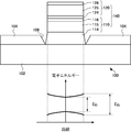
- FIG. 8 shows an example of the energy band of the light absorption structure in the semiconductor substrate 100.
- the upper part of FIG. 8 shows a cross section of the semiconductor substrate 100.
- the lower part of FIG. 8 shows the energy band of the first semiconductor 110 or the second semiconductor 120.
- the horizontal axis indicates an in-plane position parallel to the base substrate 102 in the first semiconductor 110 or the second semiconductor 120.
- the vertical axis represents the energy band of the first semiconductor 110 or the second semiconductor 120.
- the lower curve shows the upper end of the valence band, and the upper curve shows the lower end of the conduction band. The distance between the upper and lower curves indicates the forbidden bandwidth.
- the first semiconductor 110 or the second semiconductor 120 has, for example, a composition distribution having a larger forbidden band width at a position where the distance from the center of the plane parallel to the base substrate 102 is larger in the plane parallel to the base substrate 102.
- the first semiconductor 110 or the second semiconductor 120 has a composition distribution in which the forbidden band width in the peripheral portion is larger than that in the central portion.
- the first semiconductor 110 or the second semiconductor 120 has a forbidden band width of Eg 1 at the center of the first semiconductor 110 and a forbidden band of Eg 2 larger than Eg 1 at the periphery. Have a width.
- the forbidden band width is changed as shown in FIG. 8 by gradually increasing the Si composition from the central portion toward the peripheral portion.
- the second semiconductor 120 is InGaAs, a change in the forbidden band width can be obtained as shown in FIG. 8 by gradually reducing the In composition and increasing the Ga composition from the center to the periphery.
- the peripheral portion of the first semiconductor 110 or the second semiconductor 120 has a forbidden band width Eg 2 wider than the central portion, carriers generated by photoelectric conversion can be prevented from recombining in the peripheral portion.
- Any one of the first semiconductor 210, the second semiconductor 220, and the third semiconductor 230 in the photoelectric conversion device 200 has a forbidden band width that changes as shown in FIG. 8 in a plane parallel to the base substrate 202. You can do it.
- FIG. 9 shows an example of the composition distribution of the first semiconductor in the semiconductor substrate 100.
- FIG. 9A shows a cross section of the semiconductor substrate 100.
- FIG. 9B to FIG. 9E show the composition distribution of the first conduction type first semiconductor 114 included in the first semiconductor 110.
- the composition of the first semiconductor 110 changes according to the distance from the base substrate 102 in the stacking direction of the first semiconductor 110 and the second semiconductor 120.
- the ratio of silicon decreases in the direction from the surface in contact with the base substrate 102 of the first semiconductor 110 toward the second semiconductor.
- the change in the composition of Si may be continuously changed as in the examples shown in (b) to (d).
- the change in the composition of Si may change stepwise as shown in (e).
- the composition of Si in the first semiconductor 110 changes in the first conductive type first semiconductor 114 and does not change in the low carrier concentration first semiconductor 115 and the second conductive type first semiconductor 116.
- the first conductive type first semiconductor 114 is lattice-matched with the base substrate 102, and the second conductive type first semiconductor 116 and the first conductive type second semiconductor 124 are lattice-matched.
- a lattice of the base substrate 102, the first semiconductor 110, and the second semiconductor 120 has a high Si composition in a portion close to the base substrate 102 containing Si and a high Ge composition in a portion close to the Ge second semiconductor 120.
- the internal stress generated by the difference in constant can be relaxed.
- crystal defects can be improved by reducing lattice defects such as dislocations generated by internal stress.
- FIG. 10 shows an example of a cross section of the photoelectric conversion device 1000.
- the photoelectric conversion device 1000 includes a base substrate 1002, a transparent electrode 1072, a wiring 1078, a light absorption structure C1, a light absorption structure C2, a light absorption structure C3, a light collecting member 1082, and a sealing member 1084.
- the base substrate 1002 corresponds to the base substrate 202 in the photoelectric conversion device 200.
- the transparent electrode 1072 corresponds to the transparent electrode 272.
- the wiring 1078 corresponds to the wiring 278.
- the light absorption structure C1, the light absorption structure C2, and the light absorption structure C3 may have the same configuration corresponding to the light absorption structure C1 in the photoelectric conversion device 200.
- the condensing member 1082 focuses the light so that at least part of the incident light is incident on the light absorbing structure C1, the light absorbing structure C2, or the light absorbing structure C3.
- the condensing member 1082 is, for example, an optical lens.
- the light collecting member 1082 may be made of a material that transmits light, such as glass or plastic.
- the condensing member 1082 is a member having a lens effect for focusing light.
- the photoelectric conversion device 1000 may include a plurality of light collecting members 1082 corresponding to the light absorbing structures.
- the plurality of light collecting members 1082 may be integrally molded as shown in FIG.
- the condensing member 1082 is provided at a position where the converged light is incident on the light absorbing structure C1, the light absorbing structure C2, or the light absorbing structure C3.
- the condensing member 1082 includes, for example, a first color region of incident light, a second color region having a shorter wavelength region than the first color region, and a third color region having a shorter wavelength region than the second color region. Correspondingly, it has chromatic aberration with different focal length.
- FIG. 11 shows the focal position of the light collecting member having chromatic aberration.
- FIG. 11 is an enlarged view of a portion of the light absorption structure C1 in FIG.
- the light absorption structure C ⁇ b> 1 has the same configuration corresponding to the light absorption structure C ⁇ b> 1 in the photoelectric conversion device 200. In FIG. 11, some components are omitted from the description.
- the light absorption structure C1 has a three-layer tandem structure including the first semiconductor 1010, the second semiconductor 1020, and the third semiconductor 1030.
- the semiconductor 1014, the semiconductor 1016, the semiconductor 1024, the semiconductor 1026, the semiconductor 1034, and the semiconductor 1036 are the first conductive type first semiconductor 214, the second conductive type first semiconductor 216, and the first conductive type second in the photoelectric conversion device 200, respectively. This corresponds to the semiconductor 224, the second conduction type second semiconductor 226, the first conduction type third semiconductor 234, and the second conduction type third semiconductor 236.
- the condensing member 1082 has chromatic aberration, and as shown in FIG. 11, the focal points corresponding to light of each wavelength are distributed over a certain range as indicated by F01, F02 and F03.
- the focal position F01 of the condensing member 1082 with respect to light having energy corresponding to the forbidden band width of the first semiconductor 1010 is located at the position of the first space charge region in the first semiconductor 1010, that is, the low carrier concentration semiconductor 1015.
- the focal position F02 of the light collecting member 1082 with respect to light having energy corresponding to the forbidden band width of the second semiconductor 1020 is located at the position of the second space charge region in the second semiconductor 1020, that is, the low carrier concentration semiconductor 1025.
- the focal position F03 of the condensing member 1082 for light having energy corresponding to the forbidden band width of the third semiconductor 1030 is located at the position of the third space charge region in the third semiconductor 1030, that is, the low carrier concentration semiconductor 1035. Since the focal position of the light collecting member 1082 with respect to each light is equal to the position of the first space charge region, the position of the second space charge region, and the position of the third space charge region, each of the light absorption structures C1 has the first position. Light having a wavelength corresponding to the forbidden bandwidth of the first semiconductor 1010, the second semiconductor 1020, and the third semiconductor 1030 can be efficiently absorbed. Therefore, the photoelectric conversion efficiency of the photoelectric conversion device 1000 can be increased.
- the condensing member 1082 may further include an optical film that absorbs or reflects light having a wavelength longer than the wavelength corresponding to the forbidden bandwidth of the first semiconductor 1010 so as to cover the surface thereof.
- the photoelectric conversion device 1000 further includes a radiation-resistant film containing heavy metal, which is selectively disposed in a path of light incident on the light absorbing structure C1 or the like of the light collected by the light collecting member 1082. It's okay.
- a radiation-resistant film containing a heavy metal may be installed on the transparent electrode 1072.
- the sealing member 1084 integrally seals the photoelectric conversion device 1000 as shown in FIG.
- the sealing member 1084 may be made of a transparent material such as glass or plastic.
- the sealing member 1084 may be formed integrally with the light collecting member 1082.
- the condensing member 1082 may be held by the sealing member 1084.
- the wiring 1078 corresponds to the wiring 278 in the photoelectric conversion device 200.
- the wiring 1078 is connected to the transparent electrode 1072 disposed in the light absorption structure C1 or the like on the side on which incident light is incident.
- the wiring 1078 is disposed without overlapping the path through which incident light enters the transparent electrode 1072.
- the incident light may be arranged in a shadow portion that is generated when the light is collected by the light collecting member 1082. Specifically, it may be arranged in a shadow area below the broken line shown in FIG. With the above arrangement, the light focused by the light collecting member 1082 is not blocked by the wiring and enters the light absorption structure, so that the photoelectric conversion device 1000 can efficiently perform photoelectric conversion.
- FIG. 12 shows an example of the photoelectric conversion device 1200.
- the upper part of FIG. 12 shows a cross section of the photoelectric conversion device 1200.
- the lower part of FIG. 12 shows a corresponding circuit diagram of the connection state of the light absorption structure C1, the light absorption structure C2, and the light absorption structure C3.
- the photoelectric conversion device 1200 includes a base substrate 1202, a well 1203, an inhibitor 1204, a transparent electrode 1272, a wiring 1278, a light absorption structure C1, a light absorption structure C2, and a light absorption structure C3.
- the base substrate 1202 corresponds to the base substrate 202 in the photoelectric conversion device 200.
- Well 1203 corresponds to well 203.
- the transparent electrode 1272 corresponds to the transparent electrode 272.
- the wiring 1278 corresponds to the wiring 278.
- the light absorption structure C1, the light absorption structure C2, and the light absorption structure C3 correspond to the light absorption structure C1 in the photoelectric conversion device 200.
- the transparent electrode 1272 of the light absorption structure C3 is connected to the well 1203 formed below the light absorption structure C2 by the wiring 1278, and the light absorption structure A transparent electrode 1272 of C2 is connected to a well 1203 formed under the light absorbing structure C1 by a wiring 1278. That is, the light absorption structure C1, the light absorption structure C2, and the light absorption structure C3 are connected in series as shown in the corresponding circuit diagram at the bottom of FIG. In this case, the electric power generated by the photoelectric conversion device 1200 can be taken out as an electromotive force between the transparent electrode 1272 in the light absorption structure C1 and the well 1203 in the light absorption structure C3.
- FIG. 12 shows an example in which three light absorption structures are connected in series, more light absorption structures may be connected in series.
- FIG. 13 shows an example of the photoelectric conversion device 1300.
- the upper part of FIG. 13 shows a cross section of the photoelectric conversion device 1300.
- the lower part of FIG. 13 shows a corresponding circuit diagram of the connection status of the light absorption structure C1, the light absorption structure C2, and the light absorption structure C3.
- the photoelectric conversion device 1300 includes a base substrate 1302, a well 1303, an inhibitor 1304, a transparent electrode 1372, a wiring 1378, a light absorption structure C1, a light absorption structure C2, and a light absorption structure C3.
- the base substrate 1302 corresponds to the base substrate 202 in the photoelectric conversion device 200.
- Well 1303 corresponds to well 203.
- the transparent electrode 1372 corresponds to the transparent electrode 272.
- the wiring 1378 corresponds to the wiring 278.
- the light absorption structure C1, the light absorption structure C2, and the light absorption structure C3 correspond to the light absorption structure C1 in the photoelectric conversion device 200.
- the light absorbing structure C1, the light absorbing structure C2, and the transparent electrode 1272 of the light absorbing structure C3 are connected to each other by a wiring 1278.
- the light absorption structure C1, the light absorption structure C2, and the light absorption structure C3 are electrically connected to each other by a well 1303 formed in the lower part thereof. That is, the light absorption structure C1, the light absorption structure C2, and the light absorption structure C3 are connected in parallel as shown in the corresponding circuit diagram at the bottom of FIG.
- the electric power generated by the photoelectric conversion device 1300 can be taken out as an electromotive force between the transparent electrode 1372 and the well 1303.
- FIG. 13 shows an example in which three light absorption structures are connected in parallel, more light absorption structures may be connected in parallel.
- the plurality of light absorption structures connected in series or in parallel to each other may be further connected in parallel or in series with other light absorption structures connected in series or in parallel with each other.
- an inhibitor having an opening is formed on a substrate containing Si, and the first semiconductor, the second semiconductor, and the third semiconductor are epitaxially grown in the opening.
- lattice defects due to the difference in lattice constant between Si and the compound semiconductor were reduced, and a light absorption structure having a highly crystalline tandem structure could be formed. Since the crystallinity of the light absorber was increased, a photoelectric conversion device having high photoelectric conversion efficiency was obtained.
- the condensing members the light can be efficiently focused and incident on the light absorber, and the photoelectric conversion efficiency of the photoelectric conversion device can be further increased.
Landscapes
- Photovoltaic Devices (AREA)
- Life Sciences & Earth Sciences (AREA)
- Engineering & Computer Science (AREA)
- Sustainable Development (AREA)
- Sustainable Energy (AREA)
- Light Receiving Elements (AREA)
Abstract
Description
(特許文献1)特開平5-3332号公報
Claims (26)
- シリコンを含むベース基板と、
前記ベース基板上に形成され、前記ベース基板の表面を露出する開口を有し、結晶成長を阻害する阻害体と、
前記開口の内部に露出された前記ベース基板の表面に接して、前記開口の内部に形成された光吸収構造体と、
を備え、
前記光吸収構造体は、
第1伝導型第1半導体と、
前記第1伝導型第1半導体の上方に形成され、前記第1伝導型第1半導体と反対の伝導型を有する第2伝導型第1半導体と、
前記第1伝導型第1半導体と前記第2伝導型第1半導体との間に形成され、前記第1伝導型第1半導体および前記第2伝導型第1半導体よりも有効キャリア濃度が低い低キャリア濃度第1半導体と
を含む第1半導体と、
前記第2伝導型第1半導体に格子整合または擬格子整合し、前記第2伝導型第1半導体と反対の伝導型を有する第1伝導型第2半導体と、
前記第1伝導型第2半導体の上方に形成され、前記第1伝導型第2半導体と反対の伝導型を有する第2伝導型第2半導体と、
前記第1伝導型第2半導体と前記第2伝導型第2半導体との間に形成され、前記第1伝導型第2半導体および前記第2伝導型第2半導体よりも有効キャリア濃度が低い低キャリア濃度第2半導体と
を含む第2半導体と
を有する半導体基板。 - 前記光吸収構造体が、
前記第2伝導型第2半導体に格子整合または擬格子整合する第1伝導型第3半導体と、
前記第1伝導型第3半導体の上方に形成され、前記第1伝導型第3半導体と反対の伝導型を有する第2伝導型第3半導体と、
前記第1伝導型第3半導体と前記第2伝導型第3半導体との間に形成され、前記第1伝導型第3半導体および前記第2伝導型第3半導体よりも有効キャリア濃度が低い低キャリア濃度第3半導体と
を含む第3半導体をさらに有する請求項1に記載の半導体基板。 - 前記第1半導体は、第1禁制帯幅を有する材料を有し、
前記第2半導体は、前記第1禁制帯幅より大きな第2禁制帯幅を有する材料を有し、
前記第3半導体は、前記第2禁制帯幅より大きな第3禁制帯幅を有する材料を有する請求項2に記載の半導体基板。 - 前記第1半導体は、Cx1Siy1Gez1Sn1-x1-y1-z1(0≦x1<1、0≦y1≦1、0≦z1≦1、かつ0<x1+y1+z1≦1)からなり、
前記第2半導体は、Alx2Iny2Ga1-x2-y2Asz2Pw1N1-z2-w1(0≦x2≦1、0≦y2≦1、かつ0≦x2+y2≦1,および0≦z2≦1、0≦w1≦1、かつ0≦z2+w1≦1)からなり、
前記第3半導体は、Alx3Iny3Ga1-x3-y3Asz3P1-z3(0≦x3≦1、0≦y3≦1、0≦z3≦1、かつ0≦x3+y3≦1)からなる請求項3に記載の半導体基板。 - 前記光吸収構造体は、光の照射を受けてキャリアを励起し、
前記ベース基板と前記第1伝導型第1半導体との間、前記第2伝導型第1半導体と前記第1伝導型第2半導体との間、前記第2伝導型第2半導体と前記第1伝導型第3半導体との間、および前記第2伝導型第3半導体の前記低キャリア濃度第3半導体と接する面と反対の面上の少なくとも一つの位置に、前記キャリアの再結合を抑制する再結合抑制層を有する請求項2に記載の半導体基板。 - 前記光吸収構造体の側壁に接して形成された、前記側壁における前記キャリアの再結合を抑制する再結合抑制体をさらに備える請求項5に記載の半導体基板。
- 前記第2伝導型第1半導体と前記第1伝導型第2半導体との間、および、前記第2伝導型第2半導体と前記第1伝導型第3半導体との間の少なくとも一つの位置に、P型不純物が高濃度にドープされたP型不純物層およびN型不純物が高濃度にドープされたN型不純物層を有するトンネル接合層をさらに備える請求項2に記載の半導体基板。
- 前記第1半導体、前記第2半導体、および前記第3半導体から選択された1以上の半導体は、前記第1半導体、前記第2半導体、および前記第3半導体のそれぞれにおける前記ベース基板に平行な面の中心からの距離がより大きな位置において、より大きな禁制帯幅となる組成分布を有する請求項2に記載の半導体基板。
- 前記第1半導体および前記第2半導体の積層方向における前記ベース基板からの距離に応じて前記第1半導体の組成が変化している請求項1に記載の半導体基板。
- 前記第1半導体は、前記ベース基板からの距離が大きいほどシリコンの割合が少ない組成を有する請求項9に記載の半導体基板。
- 前記阻害体は複数の前記開口を有し、前記複数の開口内に形成された複数の前記光吸収構造体を備える請求項1に記載の半導体基板。
- 請求項1に記載の半導体基板を備え、前記光吸収構造体への入射光を電力に変換する光電変換デバイス。
- 前記入射光の少なくとも一部を集光して前記光吸収構造体に入射する集光部をさらに備える請求項12に記載の光電変換デバイス。
- 前記集光部は、前記入射光が含む第1色領域の光を集光して前記低キャリア濃度第1半導体に入射し、前記第1色領域より短波長域の第2色領域の光を集光して前記低キャリア濃度第2半導体に入射する請求項13に記載の光電変換デバイス。
- 前記光吸収構造体における前記入射光が入射する面に配置された透明電極と、
前記透明電極に接続された配線と
をさらに備え、
前記配線は、前記入射光が前記透明電極に入射する経路に重なることなく配置されている請求項13に記載の光電変換デバイス。 - 前記ベース基板に含まれる前記シリコンと前記光吸収構造体とが電気的に結合され、前記入射光の入射を受けて、前記透明電極と前記シリコンとの間に起電力を発生する
請求項15に記載の光電変換デバイス。 - 前記ベース基板が、前記シリコンのバルク領域から電気的に分離されかつ前記光吸収構造体と電気的に結合しているウェル領域を有し、
前記入射光の入射を受けて、前記透明電極と前記ウェル領域との間に起電力を発生する請求項15に記載の光電変換デバイス。 - 前記集光部の表面を覆い、前記第1半導体の禁制帯幅に相当する波長より長い波長の光を吸収または反射する光学膜をさらに備える請求項13に記載の光電変換デバイス。
- 前記入射光が前記光吸収構造体に入射する経路に配置された重金属を含有する耐放射線膜をさらに備える請求項13に記載の光電変換デバイス。
- 前記阻害体は複数の前記開口を有し、
前記複数の開口内に形成された複数の前記光吸収構造体を有し、
前記複数の光吸収構造体のそれぞれに対応する前記集光部を備える請求項13に記載の光電変換デバイス。 - 前記複数の光吸収構造体の各々は、互いに直列または並列に接続されている請求項20に記載の光電変換デバイス。
- 前記互いに直列または並列に接続されている前記複数の光吸収構造体は、他の互いに直列または並列に接続されている複数の光吸収構造体と並列または直列に接続されている請求項21に記載の光電変換デバイス。
- シリコンを含むベース基板の上方に阻害体を形成する段階と、
前記阻害体に、前記ベース基板の表面を露出する開口を形成する段階と、
前記開口の内部に、第1伝導型第1半導体を形成する段階と、
前記第1伝導型第1半導体の上方に、低キャリア濃度第1半導体を形成する段階と、
前記低キャリア濃度第1半導体の上方に、前記第1伝導型第1半導体と反対の伝導型を有する第2伝導型第1半導体を形成する段階と、
前記第2伝導型第1半導体の上方に、前記第2伝導型第1半導体に格子整合または擬格子整合する第1伝導型第2半導体を形成する段階と、
前記第1伝導型第2半導体の上方に、低キャリア濃度第2半導体を形成する段階と、
前記低キャリア濃度第2半導体の上方に、前記第1伝導型第2半導体と反対の伝導型を有する第2伝導型第2半導体を形成する段階と
を備え、
前記低キャリア濃度第1半導体は、前記第1伝導型第1半導体および前記第2伝導型第1半導体よりも低い有効キャリア濃度を有し、
前記低キャリア濃度第2半導体は、前記第1伝導型第2半導体および前記第2伝導型第2半導体よりも低い有効キャリア濃度を有する半導体基板の製造方法。 - 前記第1半導体を形成する段階と、前記第2半導体を形成する段階との間において、前記第1半導体を加熱する請求項23に記載の半導体基板の製造方法。
- 前記第2伝導型第2半導体の上方に、第1伝導型第3半導体を形成する段階と、
前記第1伝導型第3半導体の上方に、低キャリア濃度第3半導体を形成する段階と、
前記低キャリア濃度第3半導体の上方に、前記第1伝導型第3半導体と反対の伝導型を有する第2伝導型第3半導体を形成する段階とをさらに備える請求項23に記載の半導体基板の製造方法。 - 請求項23に記載の半導体基板の製造方法を適用して、少なくとも前記第1半導体および前記第2半導体を有する光吸収構造体を形成する段階と、
前記光吸収構造体を直列または並列に接続する段階と
を備える光電変換デバイスの製造方法。
Priority Applications (2)
| Application Number | Priority Date | Filing Date | Title |
|---|---|---|---|
| CN201080023680.9A CN102449775B (zh) | 2009-06-05 | 2010-06-03 | 半导体基板、光电转换器件、半导体基板的制造方法和光电转换器件的制造方法 |
| US13/310,614 US8835980B2 (en) | 2009-06-05 | 2011-12-02 | Semiconductor wafer, photoelectric conversion device, method of producing semiconductor wafer, and method of producing photoelectric conversion device |
Applications Claiming Priority (2)
| Application Number | Priority Date | Filing Date | Title |
|---|---|---|---|
| JP2009136665 | 2009-06-05 | ||
| JP2009-136665 | 2009-06-05 |
Related Child Applications (1)
| Application Number | Title | Priority Date | Filing Date |
|---|---|---|---|
| US13/310,614 Continuation-In-Part US8835980B2 (en) | 2009-06-05 | 2011-12-02 | Semiconductor wafer, photoelectric conversion device, method of producing semiconductor wafer, and method of producing photoelectric conversion device |
Publications (1)
| Publication Number | Publication Date |
|---|---|
| WO2010140371A1 true WO2010140371A1 (ja) | 2010-12-09 |
Family
ID=43297514
Family Applications (1)
| Application Number | Title | Priority Date | Filing Date |
|---|---|---|---|
| PCT/JP2010/003721 Ceased WO2010140371A1 (ja) | 2009-06-05 | 2010-06-03 | 半導体基板、光電変換デバイス、半導体基板の製造方法、および光電変換デバイスの製造方法 |
Country Status (6)
| Country | Link |
|---|---|
| US (1) | US8835980B2 (ja) |
| JP (1) | JP5614532B2 (ja) |
| KR (1) | KR101643021B1 (ja) |
| CN (1) | CN102449775B (ja) |
| TW (1) | TWI495119B (ja) |
| WO (1) | WO2010140371A1 (ja) |
Cited By (7)
| Publication number | Priority date | Publication date | Assignee | Title |
|---|---|---|---|---|
| CN102832117A (zh) * | 2011-06-14 | 2012-12-19 | 国际商业机器公司 | 用于形成多结光生伏打结构的剥离方法和光生伏打器件 |
| JP2013065805A (ja) * | 2011-09-15 | 2013-04-11 | Lg Electronics Inc | 薄膜太陽電池モジュール |
| WO2013088621A1 (ja) * | 2011-12-14 | 2013-06-20 | パナソニック株式会社 | 太陽電池及びその製造方法 |
| WO2013179564A1 (ja) * | 2012-05-28 | 2013-12-05 | パナソニック株式会社 | 太陽電池及びその製造方法 |
| JP2015159151A (ja) * | 2014-02-21 | 2015-09-03 | 信越化学工業株式会社 | 集光型光電変換装置及びその製造方法 |
| JP2015159154A (ja) * | 2014-02-21 | 2015-09-03 | 信越化学工業株式会社 | 集光型光電変換装置及びその製造方法 |
| EP2660874B1 (en) * | 2011-05-20 | 2016-09-14 | Panasonic Intellectual Property Management Co., Ltd. | Multi-junction compound solar cell, multi-junction compound solar battery, and method for manufacturing same |
Families Citing this family (15)
| Publication number | Priority date | Publication date | Assignee | Title |
|---|---|---|---|---|
| WO2012124807A1 (ja) * | 2011-03-16 | 2012-09-20 | 本田技研工業株式会社 | 多接合太陽電池及びその製造方法 |
| CN102315332B (zh) * | 2011-09-29 | 2013-08-07 | 英利能源(中国)有限公司 | 太阳能电池片热处理工艺 |
| WO2013076886A2 (en) * | 2011-11-21 | 2013-05-30 | Panasonic Corporation | Method for fabricating solar cell element |
| FR2992466A1 (fr) * | 2012-06-22 | 2013-12-27 | Soitec Silicon On Insulator | Procede de realisation de contact pour led et structure resultante |
| JP5921999B2 (ja) * | 2012-09-25 | 2016-05-24 | 本田技研工業株式会社 | ナノピラー型太陽電池 |
| NO348955B1 (no) | 2014-02-28 | 2025-07-28 | Pgs Geophysical As | Optisk bevegelsessensor |
| JP6287612B2 (ja) * | 2014-06-16 | 2018-03-07 | 住友電気工業株式会社 | 赤外線受光半導体素子 |
| JP6776509B2 (ja) * | 2015-05-29 | 2020-10-28 | 日産自動車株式会社 | 光電変換装置 |
| DE102015012007A1 (de) * | 2015-09-19 | 2017-03-23 | Azur Space Solar Power Gmbh | Skalierbare Spannungsquelle |
| JP6903896B2 (ja) * | 2016-01-13 | 2021-07-14 | ソニーグループ株式会社 | 受光素子の製造方法 |
| US9799736B1 (en) * | 2016-07-20 | 2017-10-24 | International Business Machines Corporation | High acceptor level doping in silicon germanium |
| CN106611804B (zh) * | 2016-12-28 | 2017-12-08 | 合肥海润光伏科技有限公司 | 一种全钝化太阳能电池结构 |
| EP3608973A1 (en) * | 2018-08-08 | 2020-02-12 | Meyer Burger Research AG | Method for manufacturing photovoltaic devices and photovoltaic devices made with the method |
| US11133207B2 (en) * | 2018-08-30 | 2021-09-28 | Taiwan Semiconductor Manufacturing Co., Ltd. | Method for forming films on wafers separated by different distances |
| CN110311006A (zh) * | 2019-07-30 | 2019-10-08 | 扬州乾照光电有限公司 | 一种提高抗辐照性能的多结太阳能电池及制作方法 |
Citations (10)
| Publication number | Priority date | Publication date | Assignee | Title |
|---|---|---|---|---|
| JPS6251272A (ja) * | 1985-08-30 | 1987-03-05 | Sharp Corp | マルチジヤンクシヨン形太陽電池 |
| JPS62102567A (ja) * | 1985-10-29 | 1987-05-13 | Sharp Corp | タンデム型太陽電池 |
| JPS62176160A (ja) * | 1986-01-30 | 1987-08-01 | Nippon Telegr & Teleph Corp <Ntt> | 化合物半導体結晶基板 |
| JPH0194677A (ja) * | 1987-10-06 | 1989-04-13 | Daido Steel Co Ltd | 半導体素子 |
| JPH02218174A (ja) * | 1989-02-17 | 1990-08-30 | Mitsubishi Electric Corp | 光電変換半導体装置 |
| JPH0394477A (ja) * | 1989-06-16 | 1991-04-19 | Canon Inc | 光起電力素子 |
| JPH04225282A (ja) * | 1990-12-26 | 1992-08-14 | Canon Inc | 太陽電池およびその製造方法 |
| JPH07321357A (ja) * | 1994-05-27 | 1995-12-08 | Sanyo Electric Co Ltd | 光起電力装置 |
| JP2001093849A (ja) * | 1999-09-22 | 2001-04-06 | Canon Inc | 液相成長法、エピタキシャル基体の製造方法、および太陽電池の製造方法 |
| JP2008124381A (ja) * | 2006-11-15 | 2008-05-29 | Sharp Corp | 太陽電池 |
Family Cites Families (31)
| Publication number | Priority date | Publication date | Assignee | Title |
|---|---|---|---|---|
| US2949498A (en) * | 1955-10-31 | 1960-08-16 | Texas Instruments Inc | Solar energy converter |
| JPS60210831A (ja) | 1984-04-04 | 1985-10-23 | Agency Of Ind Science & Technol | 化合物半導体結晶基板の製造方法 |
| JPH073814B2 (ja) | 1984-10-16 | 1995-01-18 | 松下電器産業株式会社 | 半導体基板の製造方法 |
| US4614564A (en) | 1984-12-04 | 1986-09-30 | The United States Of America As Represented By The United States Department Of Energy | Process for selectively patterning epitaxial film growth on a semiconductor substrate |
| JPS61188927A (ja) | 1985-02-15 | 1986-08-22 | Sharp Corp | 化合物半導体装置 |
| JPH077841B2 (ja) * | 1986-03-28 | 1995-01-30 | 沖電気工業株式会社 | 化合物半導体太陽電池の製造方法 |
| US5158907A (en) * | 1990-08-02 | 1992-10-27 | At&T Bell Laboratories | Method for making semiconductor devices with low dislocation defects |
| US5403771A (en) | 1990-12-26 | 1995-04-04 | Canon Kabushiki Kaisha | Process for producing a solar cell by means of epitaxial growth process |
| US5091767A (en) * | 1991-03-18 | 1992-02-25 | At&T Bell Laboratories | Article comprising a lattice-mismatched semiconductor heterostructure |
| JPH0793452B2 (ja) | 1991-06-25 | 1995-10-09 | 株式会社日立製作所 | タンデムヘテロ光電変換素子の製造方法 |
| JP3170105B2 (ja) * | 1993-07-01 | 2001-05-28 | キヤノン株式会社 | 太陽電池モジュール |
| JP3935237B2 (ja) * | 1997-03-11 | 2007-06-20 | キヤノン株式会社 | 光電気変換体及び建材 |
| JP2000252492A (ja) * | 1999-02-25 | 2000-09-14 | Sumitomo Electric Ind Ltd | 太陽電池、この製造方法、および積層型太陽電池 |
| JP4054480B2 (ja) * | 1999-05-18 | 2008-02-27 | キヤノン株式会社 | Si基板上の光電融合デバイス構造、その製造方法、及び成膜方法 |
| JP3577430B2 (ja) * | 1999-06-09 | 2004-10-13 | シャープ株式会社 | 太陽電池セルおよびその製造方法 |
| JP2001189470A (ja) * | 1999-12-28 | 2001-07-10 | Fuji Electric Co Ltd | 積層型アモルファスシリコン太陽電池の安定化方法および安定化装置 |
| CN100477289C (zh) * | 2004-01-20 | 2009-04-08 | 瑟雷姆技术公司 | 具有外延生长量子点材料的太阳能电池 |
| JP4863792B2 (ja) * | 2006-07-05 | 2012-01-25 | 日軽金アクト株式会社 | 太陽光発電装置 |
| WO2008036256A1 (en) | 2006-09-18 | 2008-03-27 | Amberwave Systems Corporation | Aspect ratio trapping for mixed signal applications |
| DE112008002387B4 (de) * | 2007-09-07 | 2022-04-07 | Taiwan Semiconductor Manufacturing Co., Ltd. | Struktur einer Mehrfachübergangs-Solarzelle, Verfahren zur Bildung einer photonischenVorrichtung, Photovoltaische Mehrfachübergangs-Zelle und Photovoltaische Mehrfachübergangs-Zellenvorrichtung, |
| KR20100096084A (ko) | 2007-12-28 | 2010-09-01 | 스미또모 가가꾸 가부시키가이샤 | 반도체 기판, 반도체 기판의 제조 방법 및 전자 디바이스 |
| CN101896999B (zh) | 2007-12-28 | 2012-08-08 | 住友化学株式会社 | 半导体基板、半导体基板的制造方法及电子器件 |
| US20110012175A1 (en) | 2007-12-28 | 2011-01-20 | Sumitomo Chemical Company, Limited | Semiconductor wafer, semiconductor wafer manufacturing method, and electronic device |
| CN103367115A (zh) | 2007-12-28 | 2013-10-23 | 住友化学株式会社 | 半导体基板、半导体基板的制造方法及电子器件 |
| US20110006399A1 (en) | 2007-12-28 | 2011-01-13 | Sumitomo Chemical Company, Limited | Semiconductor wafer and semiconductor wafer manufacturing method |
| JP5669359B2 (ja) | 2008-03-01 | 2015-02-12 | 住友化学株式会社 | 半導体基板、半導体基板の製造方法および電子デバイス |
| CN101952937B (zh) | 2008-03-01 | 2012-11-07 | 住友化学株式会社 | 半导体基板、半导体基板的制造方法及电子装置 |
| DE102008029306A1 (de) | 2008-06-20 | 2009-12-24 | Bayer Technology Services Gmbh | Schneckenelemente mit reduziertem Energieeintrag beim Druckaufbau |
| CN102171790A (zh) | 2008-10-02 | 2011-08-31 | 住友化学株式会社 | 半导体基板、电子器件、以及半导体基板的制造方法 |
| KR20110065444A (ko) | 2008-10-02 | 2011-06-15 | 스미또모 가가꾸 가부시키가이샤 | 반도체 기판, 전자 디바이스 및 반도체 기판의 제조 방법 |
| US20110186911A1 (en) | 2008-10-02 | 2011-08-04 | Sumitomo Chemical Company, Limited | Semiconductor substrate, electronic device and method for manufacturing semiconductor substrate |
-
2010
- 2010-06-03 CN CN201080023680.9A patent/CN102449775B/zh not_active Expired - Fee Related
- 2010-06-03 KR KR1020117026326A patent/KR101643021B1/ko not_active Expired - Fee Related
- 2010-06-03 WO PCT/JP2010/003721 patent/WO2010140371A1/ja not_active Ceased
- 2010-06-04 TW TW099118116A patent/TWI495119B/zh not_active IP Right Cessation
- 2010-06-04 JP JP2010128367A patent/JP5614532B2/ja not_active Expired - Fee Related
-
2011
- 2011-12-02 US US13/310,614 patent/US8835980B2/en not_active Expired - Fee Related
Patent Citations (10)
| Publication number | Priority date | Publication date | Assignee | Title |
|---|---|---|---|---|
| JPS6251272A (ja) * | 1985-08-30 | 1987-03-05 | Sharp Corp | マルチジヤンクシヨン形太陽電池 |
| JPS62102567A (ja) * | 1985-10-29 | 1987-05-13 | Sharp Corp | タンデム型太陽電池 |
| JPS62176160A (ja) * | 1986-01-30 | 1987-08-01 | Nippon Telegr & Teleph Corp <Ntt> | 化合物半導体結晶基板 |
| JPH0194677A (ja) * | 1987-10-06 | 1989-04-13 | Daido Steel Co Ltd | 半導体素子 |
| JPH02218174A (ja) * | 1989-02-17 | 1990-08-30 | Mitsubishi Electric Corp | 光電変換半導体装置 |
| JPH0394477A (ja) * | 1989-06-16 | 1991-04-19 | Canon Inc | 光起電力素子 |
| JPH04225282A (ja) * | 1990-12-26 | 1992-08-14 | Canon Inc | 太陽電池およびその製造方法 |
| JPH07321357A (ja) * | 1994-05-27 | 1995-12-08 | Sanyo Electric Co Ltd | 光起電力装置 |
| JP2001093849A (ja) * | 1999-09-22 | 2001-04-06 | Canon Inc | 液相成長法、エピタキシャル基体の製造方法、および太陽電池の製造方法 |
| JP2008124381A (ja) * | 2006-11-15 | 2008-05-29 | Sharp Corp | 太陽電池 |
Cited By (12)
| Publication number | Priority date | Publication date | Assignee | Title |
|---|---|---|---|---|
| EP2660874B1 (en) * | 2011-05-20 | 2016-09-14 | Panasonic Intellectual Property Management Co., Ltd. | Multi-junction compound solar cell, multi-junction compound solar battery, and method for manufacturing same |
| CN102832117A (zh) * | 2011-06-14 | 2012-12-19 | 国际商业机器公司 | 用于形成多结光生伏打结构的剥离方法和光生伏打器件 |
| GB2492439B (en) * | 2011-06-14 | 2013-09-18 | Ibm | Method of cleaving a semiconductor material |
| US8927318B2 (en) | 2011-06-14 | 2015-01-06 | International Business Machines Corporation | Spalling methods to form multi-junction photovoltaic structure |
| JP2013065805A (ja) * | 2011-09-15 | 2013-04-11 | Lg Electronics Inc | 薄膜太陽電池モジュール |
| WO2013088621A1 (ja) * | 2011-12-14 | 2013-06-20 | パナソニック株式会社 | 太陽電池及びその製造方法 |
| JP5422082B2 (ja) * | 2011-12-14 | 2014-02-19 | パナソニック株式会社 | 太陽電池及びその製造方法 |
| EP2763186A4 (en) * | 2011-12-14 | 2015-01-07 | Panasonic Corp | SOLAR CELL AND METHOD FOR THE PRODUCTION THEREOF |
| US9306095B2 (en) | 2011-12-14 | 2016-04-05 | Panasonic Intellectual Property Management Co., Ltd. | Solar cell and method for manufacturing same |
| WO2013179564A1 (ja) * | 2012-05-28 | 2013-12-05 | パナソニック株式会社 | 太陽電池及びその製造方法 |
| JP2015159151A (ja) * | 2014-02-21 | 2015-09-03 | 信越化学工業株式会社 | 集光型光電変換装置及びその製造方法 |
| JP2015159154A (ja) * | 2014-02-21 | 2015-09-03 | 信越化学工業株式会社 | 集光型光電変換装置及びその製造方法 |
Also Published As
| Publication number | Publication date |
|---|---|
| US8835980B2 (en) | 2014-09-16 |
| CN102449775A (zh) | 2012-05-09 |
| US20120074463A1 (en) | 2012-03-29 |
| KR20120018143A (ko) | 2012-02-29 |
| CN102449775B (zh) | 2014-07-02 |
| JP5614532B2 (ja) | 2014-10-29 |
| TW201108423A (en) | 2011-03-01 |
| KR101643021B1 (ko) | 2016-07-26 |
| JP2011014897A (ja) | 2011-01-20 |
| TWI495119B (zh) | 2015-08-01 |
Similar Documents
| Publication | Publication Date | Title |
|---|---|---|
| JP5614532B2 (ja) | 半導体基板、光電変換デバイス、半導体基板の製造方法、および光電変換デバイスの製造方法 | |
| JP6461278B2 (ja) | 半導体ベースのマルチ接合光起電力デバイスの製造方法 | |
| US10050166B2 (en) | Silicon heterojunction photovoltaic device with wide band gap emitter | |
| JP3657143B2 (ja) | 太陽電池及びその製造方法 | |
| US20090165855A1 (en) | Passivation layer structure of solar cell and fabricating method thereof | |
| US9324911B2 (en) | Methods of fabricating dilute nitride semiconductor materials for use in photoactive devices and related structures | |
| JP2010512664A (ja) | 酸化亜鉛多接合光電池及び光電子装置 | |
| JP5669254B2 (ja) | センサ、半導体基板、および半導体基板の製造方法 | |
| KR20120088719A (ko) | 개선된 광전지 | |
| US20150122329A1 (en) | Silicon heterojunction photovoltaic device with non-crystalline wide band gap emitter | |
| US9337377B2 (en) | Methods of forming dilute nitride materials for use in photoactive devices and related structures | |
| JP2014220351A (ja) | 多接合太陽電池 | |
| JP2001028452A (ja) | 光電変換装置 | |
| JP4986056B2 (ja) | 集光式光電変換装置 |
Legal Events
| Date | Code | Title | Description |
|---|---|---|---|
| WWE | Wipo information: entry into national phase |
Ref document number: 201080023680.9 Country of ref document: CN |
|
| 121 | Ep: the epo has been informed by wipo that ep was designated in this application |
Ref document number: 10783159 Country of ref document: EP Kind code of ref document: A1 |
|
| ENP | Entry into the national phase |
Ref document number: 20117026326 Country of ref document: KR Kind code of ref document: A |
|
| NENP | Non-entry into the national phase |
Ref country code: DE |
|
| 122 | Ep: pct application non-entry in european phase |
Ref document number: 10783159 Country of ref document: EP Kind code of ref document: A1 |