WO2010134552A1 - はんだコート部品、その製造方法及びその実装方法 - Google Patents
はんだコート部品、その製造方法及びその実装方法 Download PDFInfo
- Publication number
- WO2010134552A1 WO2010134552A1 PCT/JP2010/058466 JP2010058466W WO2010134552A1 WO 2010134552 A1 WO2010134552 A1 WO 2010134552A1 JP 2010058466 W JP2010058466 W JP 2010058466W WO 2010134552 A1 WO2010134552 A1 WO 2010134552A1
- Authority
- WO
- WIPO (PCT)
- Prior art keywords
- solder
- frame member
- treatment
- mounting
- coated
- Prior art date
- Legal status (The legal status is an assumption and is not a legal conclusion. Google has not performed a legal analysis and makes no representation as to the accuracy of the status listed.)
- Ceased
Links
Images


Classifications
-
- B—PERFORMING OPERATIONS; TRANSPORTING
- B23—MACHINE TOOLS; METAL-WORKING NOT OTHERWISE PROVIDED FOR
- B23K—SOLDERING OR UNSOLDERING; WELDING; CLADDING OR PLATING BY SOLDERING OR WELDING; CUTTING BY APPLYING HEAT LOCALLY, e.g. FLAME CUTTING; WORKING BY LASER BEAM
- B23K1/00—Soldering, e.g. brazing, or unsoldering
- B23K1/0008—Soldering, e.g. brazing, or unsoldering specially adapted for particular articles or work
- B23K1/0016—Brazing of electronic components
-
- B—PERFORMING OPERATIONS; TRANSPORTING
- B23—MACHINE TOOLS; METAL-WORKING NOT OTHERWISE PROVIDED FOR
- B23K—SOLDERING OR UNSOLDERING; WELDING; CLADDING OR PLATING BY SOLDERING OR WELDING; CUTTING BY APPLYING HEAT LOCALLY, e.g. FLAME CUTTING; WORKING BY LASER BEAM
- B23K1/00—Soldering, e.g. brazing, or unsoldering
- B23K1/20—Preliminary treatment of work or areas to be soldered, e.g. in respect of a galvanic coating
-
- B—PERFORMING OPERATIONS; TRANSPORTING
- B23—MACHINE TOOLS; METAL-WORKING NOT OTHERWISE PROVIDED FOR
- B23K—SOLDERING OR UNSOLDERING; WELDING; CLADDING OR PLATING BY SOLDERING OR WELDING; CUTTING BY APPLYING HEAT LOCALLY, e.g. FLAME CUTTING; WORKING BY LASER BEAM
- B23K35/00—Rods, electrodes, materials, or media, for use in soldering, welding, or cutting
- B23K35/02—Rods, electrodes, materials, or media, for use in soldering, welding, or cutting characterised by mechanical features, e.g. shape
- B23K35/0222—Rods, electrodes, materials, or media, for use in soldering, welding, or cutting characterised by mechanical features, e.g. shape for use in soldering, brazing
- B23K35/0233—Sheets, foils
- B23K35/0238—Sheets, foils layered
-
- B—PERFORMING OPERATIONS; TRANSPORTING
- B23—MACHINE TOOLS; METAL-WORKING NOT OTHERWISE PROVIDED FOR
- B23K—SOLDERING OR UNSOLDERING; WELDING; CLADDING OR PLATING BY SOLDERING OR WELDING; CUTTING BY APPLYING HEAT LOCALLY, e.g. FLAME CUTTING; WORKING BY LASER BEAM
- B23K35/00—Rods, electrodes, materials, or media, for use in soldering, welding, or cutting
- B23K35/22—Rods, electrodes, materials, or media, for use in soldering, welding, or cutting characterised by the composition or nature of the material
- B23K35/24—Selection of soldering or welding materials proper
- B23K35/26—Selection of soldering or welding materials proper with the principal constituent melting at less than 400 degrees C
- B23K35/262—Sn as the principal constituent
-
- H—ELECTRICITY
- H05—ELECTRIC TECHNIQUES NOT OTHERWISE PROVIDED FOR
- H05K—PRINTED CIRCUITS; CASINGS OR CONSTRUCTIONAL DETAILS OF ELECTRIC APPARATUS; MANUFACTURE OF ASSEMBLAGES OF ELECTRICAL COMPONENTS
- H05K9/00—Screening of apparatus or components against electric or magnetic fields
- H05K9/0007—Casings
- H05K9/002—Casings with localised screening
- H05K9/0022—Casings with localised screening of components mounted on printed circuit boards [PCB]
- H05K9/0024—Shield cases mounted on a PCB, e.g. cans or caps or conformal shields
- H05K9/0032—Shield cases mounted on a PCB, e.g. cans or caps or conformal shields having multiple parts, e.g. frames mating with lids
Definitions
- the present invention relates to a shield case that electromagnetically shields an electronic component mounted on a substrate, a solder coated component applicable to a substrate reinforcing frame that reinforces a short, small and thin substrate, a manufacturing method thereof, and a mounting method thereof. .
- a shield case is a metal molded part that is mounted on a board, and a method of soldering a claw part extending from the shield case to a wiring pattern on the back side of the board via an insertion part opened in the board, A method of surface mounting a mounting part of a shield case on a land pattern provided on a surface is known. Soldering is also performed in surface mounting.
- the shield case is often used for the purpose of protecting the precision module from external force.
- housing parts such as shield cases and board reinforcement frames are made of white materials (Cu-Zn-Ni / C7521R, C7701R, etc.) due to their magnetic resistance, rust resistance, oxidation resistance, thermal expansion resistance, and workability.
- a metal member made of stainless steel (SUS304, SUS316, SUS430, etc.) is often used.
- the finish workability is slightly difficult for the white material (C7521R, C7701R, etc.), and the stainless material (SUS304, SUS316, SUS430, etc.) is easy.
- the solder wettability is slightly easier for white materials and difficult for stainless materials.
- Patent Document 1 discloses a shield case mounting structure.
- the substrate, the shield case, and the fixing member are provided.
- the board has an insertion part and an electronic component is mounted on one surface.
- the shield case has a protrusion and covers the electronic component to block electromagnetic waves.
- the protruding portion protruding from the shield case is inserted into the insertion portion of the substrate.
- the fixing member fixes the protruding portion inserted into the insertion portion on the other surface of the substrate.
- Patent Document 1 JP 2006-196664 A
- the shield case found in Patent Document 1
- many are manufactured by bending a sheet metal, and a gap is formed between adjacent side surfaces.
- the shield case is fixed to the substrate by soldering the claw portion extending from the side surface to a land pattern provided on the substrate.
- the mounting substrate to which the shield case is attached has also been miniaturized. This miniaturization tends to reduce the area of the land pattern for soldering. When the area of the land pattern is reduced, workability such as a longer time for soldering work is deteriorated.
- the soldering area is reduced, the solder can be easily removed, and the bonding strength of the shield case to the board is weakened in strength.
- the soldering surface of a casing part such as a shield case or a board reinforcing frame is subjected to a surface treatment before the soldering process.
- a surface treatment at this time, degreasing treatment, rust prevention treatment, plating treatment or the like is performed. Degreasing and rust prevention treatments are only for surface cleansing and protective effects, and good soldering is difficult.
- the plating treatment a single unit of tin having a thickness of several microns, or binary solder base plating such as tin silver or tin copper is applied.
- the solder is applied only to the substrate side, and no solder is applied to the case component side. Since the amount of solder is small and solder wettability is poor, the problem of soldering such as difficulty in forming a satisfactory fillet during surface mounting has not been solved.
- a solder coated component is provided with a nickel film and a tin alloy plating film of a predetermined thickness on a base material in order, and lead-free molten solder is formed on the tin alloy plating film. It comprises a metal member that has been subjected to a surface treatment that has been coated.
- solder coat component for example, a metal member is processed into a shield component shape, and thereafter a nickel film and a tin alloy plating film having a predetermined thickness are sequentially formed on one part or all parts of the metal member. Then, a surface treatment is performed by applying a molten solder coating to a part or all of the part on the metal member after the surface treatment, and a part of the shield part shape is a soldering surface for surface mounting. It has been.
- Lead-free molten solder includes Sn-Ag, Sn-Cu, Sn-Ag-Cu, Sn-Bi, Sn-Ag-Cu-Bi, Sn-Bi-Ag (Cu), Sn A lead-free solder such as -Ag-Cu-Ni or Sn-Ag-Cu-Sb is used.
- solder wettability of the soldered part of the surface-mounted solder-coated component is further improved (becomes better) than the conventional plating method, soldering treatment by rust prevention treatment, degreasing treatment, etc. become able to.
- the method for producing a solder coated component according to the present invention includes a step of sequentially forming a nickel film and a tin alloy plating film having a predetermined thickness on a metal member for solder coated components, and performing a base treatment, and the tin alloy plating subjected to the ground treatment And a surface treatment process including a process of coating a lead-free molten solder on the film.
- the solder of the soldered part of the solder coated part for surface mounting is compared with the plating method of the conventional example and the soldering process by rust prevention process, degreasing process, etc.
- the wettability can be further improved.
- the first mounting method of the solder coat component according to the present invention includes a step of processing a metal member for solder coat component to form a shield component for surface mounting, and the metal formed on the shield component.
- a surface treatment step consisting of a step of sequentially forming a nickel film and a tin alloy plating film of a predetermined thickness on the member, and a step of coating the molten metal on the metal member that has been subjected to the ground treatment, Forming a solder material on a predetermined portion of the mounting substrate; and aligning the shield component for surface mounting on the predetermined portion of the mounting substrate on which the solder material is formed, and performing a heat treatment, and the mounting substrate and the shield. And a step of joining the parts.
- a nickel film and a tin alloy plating film having a predetermined film thickness are sequentially formed on a metal member which is a base material for the solder coated component.
- a surface treatment step comprising a step of processing and a step of coating the molten metal on the metal member that has been ground-treated, a step of processing the surface-treated metal member to form a shield component for surface mounting,
- solder-coated components for surface mounting compared to the conventional plating method and the soldering processing by rust prevention processing, degreasing processing, etc. It has become possible to further improve the solder wettability of the soldered portion of the solder.
- the solder coated component for surface mounting is compared with the plating method of the conventional example and the soldering treatment by rust prevention treatment, degreasing treatment, etc.
- the solder wettability of the soldered part can be further improved.
- a soldered portion can be formed in the entire range of an arbitrary soldering region of a casing component that cannot be obtained by a conventional metal member.
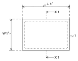
- FIG. 3 is a cross-sectional view illustrating a configuration example of a frame member 11 of a shield case 100. It is a top view which shows the example of formation (the 1) at the time of drawing processing of the white material 1 which concerns on the frame member 11.
- FIG. 3B is a cross-sectional view taken along arrow X1-X1 in FIG. It is a top view which shows the example of a formation at the time of the drawing process of the white material 1 which concerns on the frame member 11 (the 2). It is a side view which shows the example of formation (the 2) at the time of drawing processing of the white material 1 which concerns on the frame member 11.
- FIG. 3 is a cross-sectional view illustrating a configuration example of a frame member 11 of a shield case 100. It is a top view which shows the example of formation (the 1) at the time of drawing processing of the white material 1 which concerns on the frame member 11.
- FIG. 3B is a cross-sectional view taken along arrow X1-X1 in FIG. It is
- FIG. 5B is a cross-sectional view taken along the line X1′-X1 ′ of FIG.
- FIG. 6 is a process diagram showing an example (part 1) of mounting the frame member 11 according to the shield case 100 on the printed wiring board 10;
- FIG. 11 is a process diagram showing an example (part 2) of mounting the frame member 11 according to the shield case 100 on the printed wiring board 10;
- FIG. 11 is a process diagram illustrating an example (No. 3) of mounting the frame member 11 according to the shield case 100 on the printed wiring board 10;
- FIG. 10B is a cross-sectional view taken along arrow X3-X3 in FIG.
- FIG. 6 is a process diagram illustrating an example (part 1) of mounting the frame member 21 according to the shield case 200 on the printed wiring board 10;
- FIG. 11 is a process diagram illustrating an example (part 2) of mounting the frame member 21 according to the shield case 200 on the printed wiring board 10;
- FIG. 11 is a process diagram illustrating an example (No. 3) of mounting the frame member 21 according to the shield case 200 on the printed wiring board 10;
- It is a perspective view which shows the structural example of the tuner case 300 as 3rd Embodiment.
- the nickel coating and the tin alloy plating film having a predetermined film thickness are sequentially formed as compared with the case where only the tin film treatment or the like is applied to the metal member for plating treatment.
- the present invention has been achieved by paying attention to the point that a molten solder having a film thickness of several tens of times can be deposited on the tin alloy plating film.
- the present invention makes it possible to form a fillet portion in the entire range of an arbitrary soldering region of a casing component without using a highly corrosive and highly active flux, and generates a solder unjoined portion, a void, or the like.
- An object of the present invention is to provide a solder-coated component that can be securely and firmly bonded to a substrate, a manufacturing method thereof, and a mounting method thereof.
- a solder coated component, a manufacturing method thereof, and a mounting method thereof will be described with reference to the drawings.
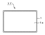
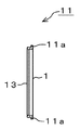
- a shield case 100 as the first embodiment shown in FIG. 1 constitutes an example of a solder coated component, and electromagnetically shields an electronic component (not shown) mounted on the printed wiring board 10.
- the solder coated part is a metal part such as a shield case, in which a nickel film and a tin alloy plating film having a predetermined thickness are sequentially provided, and a lead-free molten solder film is formed on the tin alloy plating film.
- the base material refers to a forming material such as a shield case, and the base material is composed of a material of a metal member such as iron or Kovar in addition to white or stainless steel.
- the predetermined nickel film refers to a nickel film having a plating thickness of 0.3 to 2.0 ⁇ m, more preferably 0.5 to 1.0 ⁇ m.
- the predetermined tin alloy film means a tin alloy film having a plating thickness of 0.7 to 7.0 ⁇ m, more preferably 1.0 to 3.0 ⁇ m.
- the shield case 100 includes a frame member 11 and a lid member 12.
- the frame member 11 has a frame shape having a width W1, a length L1, and a height H1.
- the frame member 11 has a width W1 of about 38 mm, a length L1 of about 60 mm, and a height H1 of about 2 mm.
- the frame member 11 is soldered to the printed wiring board 10.
- the printed wiring board 10 is provided with a land pattern 10a obtained by patterning a copper foil, and the frame member 11 is melted and soldered to the land pattern 10a by a reflow process.
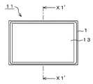
- An opening 13 is formed in the frame of the frame member 11.
- the electronic components in the opening 13 can be inspected.
- a hat-shaped (saddle-shaped) drawn end portion 11a is provided around the opening 13 during drawing.
- the throttle end portion 11a is provided to reinforce the frame member 11, strengthen the lid member 12, and improve the wettability of the molten solder during the reflow process.
- the lid member 12 has a rectangular cover shape, and is attached so as to be openable so as to cover (cover) the frame member 11 soldered to the printed wiring board 10.
- the lid member 12 is composed of a tin member (tin-plated steel plate), a white material (C7521R, C7701R, etc.), a stainless material (SUS304, SUS316, SUS430, etc.).
- the lid member 12 is formed by cutting and bending these plate-like members.
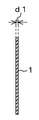
- the frame member 11 of the shield case 100 is composed of a white material 1 constituting an example of a metal member as shown in FIG.
- the western white material 1 has a predetermined thickness d.
- the white wood 1 is provided with a nickel (Ni) plating layer 2 (film) and a tin-copper (Sn—Cu) plating layer 3 (film) having a predetermined thickness in order from the lower layer, and the Sn On the Cu plating layer 3, molten solder is coated (coated).
- the layer coated with molten solder is referred to as a solder coat layer 4.
- a treatment layer composed of a nickel (Ni) plating layer 2 (film), a tin-copper (Sn—Cu) plating layer 3 (film), and a solder coat layer 4 is referred to as a surface treatment layer 5.
- the coating process when forming the coating layer 4 coated with the above-described molten solder is a method in which a metal member is immersed in the molten solder so that the entire solder is deposited or soldered locally. This is a surface treatment in which solder is deposited only on the necessary parts of the metal member.
- the thickness of the solder coat layer 4 is secured to about 10 ⁇ m to 30 ⁇ m in order to improve the wettability of the molten solder during the reflow process.
- molten solder for example, Sn—Ag—Cu-based lead-free solder is used.
- molten solder includes Sn-Ag, Sn-Cu, Sn-Bi, Sn-Ag-Cu-Bi, Sn-Bi-Ag (Cu), Sn -Ag-Cu-Ni-based or Sn-Ag-Cu-Sb-based alloy solder (Eco Solder (registered trademark) M705) is used.
- the composition of the M705 molten solder is Sn-3.0Ag-0.5Cu.
- Eco Solder (registered trademark) M20 is used.
- the composition of the molten solder of M20 is Sn-0.75Cu.
- the surface treatment layer 5 of the present invention is provided with a nickel (Ni) plating layer 2 (film) and a tin-copper (Sn—Cu) plating layer 3 (film) in sequence, and
- the Sn—Cu plating layer 3 is composed of a solder coat layer 4 formed by coating (coating treatment) with molten solder.
- the frame member 11 will be described with reference to FIGS. 3A to 5B with respect to the manufacturing method of the shield case 100 according to the present invention.
- the white material 1 constituting an example of the metal member for the shield case is processed into a shield part shape before the surface treatment.
- the shield case 100 is formed by processing the white material 1 to form the frame member 11 for surface mounting.
- a case where the western white material 1 that can be subjected to the molten solder coating is drawn to form a drawn end portion for surface mounting on the frame member 11 is taken as an example.
- Eco Solder M705 registered trademark used for the soldering process when the shield case is mounted is coated with solder on both sides of the shield case with 15 ⁇ m on one side.
- FIG. 3B is a cross-sectional view of the western white material 1 taken along arrow X1-X1.
- stainless steel SUS304, SUS316, SUS430, etc.
- the thickness d1 of the white material 1 is, for example, 0.1 mm, 0.15 mm, 0.2 mm, 0.25 mm, 0.3 mm, or the like.
- the width W1 ′ of the white material 1 is slightly larger (about 5% to 10%) than the width W1 of the finished dimension of the frame member 11 in order to obtain the height H1 by drawing, and the length L1 ′. Also, a frame member 11 having a slightly longer length (about 5% to 10%) than the length L1 of the finished dimension of the frame member 11 is prepared.
- the broken line in the figure is a portion (projection portion) to which a projection tip pressing portion of a drawing machine (not shown) is applied.
- the drawing machine is equipped with an end pressing mechanism for forming the drawn end 11a so that a part of the frame member 11 becomes a soldering surface for surface mounting.
- FIG. 1 a case where a hat-shaped (butterfly-shaped) narrow end 11 a is provided around the aperture bend opening 13 in an L shape around the outer periphery of the white material 1 is taken as an example.
- the white material 1 having the size shown in FIGS. 3A and 3B is prepared, the white material 1 is set on a drawing machine (not shown), and the convex portion tip pressing portion is pressed against the white material 1.
- the drawing process is executed.
- the hat-shaped white material 1 shown in FIG. 4A can be obtained.
- the convex part 1a is comprised.
- the outer periphery is a bowl-shaped throttle end 11a.
- a hat-shaped intermediate member 11 ′ in which the opening 13 of the frame member 11 as shown in FIG. 1 is not yet opened is obtained.
- the opening 13 is formed in the convex portion 1 a of the intermediate member 11 ′.
- the opening 13 is formed, for example, by setting the intermediate member 11 ′ on a press machine and punching with the press member. Thereby, the fabric frame member 11 having the opening 13 shown in FIG. 5A can be obtained.
- FIG. 5B shows a cross-sectional view of the frame member 11 taken along the arrow X1'-X1 '.
- the processing step for obtaining the frame member 11 can be selected as appropriate, for example, by continuously forming from a hoop material of the white material 1 wound in a roll shape with a progressive press.
- the fabric frame member 11 shown in FIG. 5A and FIG. 5B When the fabric frame member 11 shown in FIG. 5A and FIG. 5B is prepared, nickel (Ni) and tin copper (Sn—Cu) having a predetermined film thickness are sequentially formed on the frame member 11 to perform the base treatment.
- the degreasing process of the frame member 11 is performed. According to this degreasing process, pre-processing of the frame member 11 is performed using NaOH (sodium hydroxide) or NaCN (sodium cyanide).
- the cyanide immersion degreasing and / or cyanide electrolytic degreasing step is performed on the pre-treated frame member 11.
- Ni plating is applied to the frame member 11 after the degreasing treatment.
- the frame member 11 is set in an electroplating apparatus (not shown), and the base processing is executed.
- an electrolytic solution is filled in a plating bath.
- the frame member 11 is connected to the cathode electrode, and the target material such as Ni is connected to the anode electrode to pass a direct current.
- Ni plating is applied to the first layer on the western white material 1 by electroplating.
- the plating bath constitutes a sulfonic acid bath.
- the electrolytic solution is composed of a Ni plating solution.
- Ni plating solution nickel sulfamate (Ni (NH2SO3) 2 ⁇ 4H2O) or nickel chloride (NiCl2 ⁇ 6H2O) is used.
- Ni plating layer 2 can be provided on the upper layer of the white material 1 as shown in FIG.
- the generation of whiskers can be prevented by applying the Ni plating layer 2 to the upper layer of the white material 1.
- the upper layer of the Ni plating layer 2 is subjected to Sn—Cu plating by electroplating.
- the frame member 11 is immersed in an acid immersion bath for a short time, and the metal surface of the Ni plating layer 2 is subjected to a gloss treatment.
- H2SO4 sulfuric acid
- an organic acid bath is used as the plating bath 51.
- methanesulfonic acid CH3SO3H
- tin metalsulfamate CH3SO3Sn
- an electrolytic bath containing copper ions or copper complex ions is used for the plating bath.
- an electrolytic solution containing copper ions or copper complex ions is used as the Cu plating solution.
- Metal copper is used for the cathode electrode.
- the Sn—Cu plating layer 3 can be provided on the Ni plating layer 2 as shown in FIG. Note that phosphoric acid is used for the antioxidant treatment of the frame member 11.
- a method of plating a method of immersing a metal member as described above and plating it entirely, a part of a metal member that is necessary to be plated by a stamp plating method, or a means can be selected as appropriate. .
- Eco Solder M705 is a lead-free molten solder.
- Lead-free molten solder includes Sn-Ag, Sn-Cu, Sn-Ag-Cu, Sn-Bi, Sn-Ag-Cu-Bi, Sn-Bi-Ag (Cu), Sn Use lead-free solder such as -Ag-Cu-Ni or Sn-Ag-Cu-Sb.
- the coating thickness of the lead-free molten solder was about 15 ⁇ m per one side of the metal member such as the white material 1, and this coating treatment was performed on one side and / or both sides.
- the control of the coat thickness is adjusted by using a known technique for controlling by applying ultrasonic waves to the molten solder immersed in the metal member, for example.
- the solder coat layer 4 can be provided on the upper layer of the Sn—Cu plating layer 3 as shown in FIG.
- the frame member 11 for the shield case after the surface treatment is packed in embossed tape, wound on a reel, and conveyed to the component supply path. Alternatively, it is packed on a general-purpose or dedicated tray and conveyed to the component supply path.
- the surface treatment consisting of a nickel film and a tin alloy plating film undercoating, and a coating process using molten solder is performed by selecting a known appropriate means such as a stamp plating method or a local soldering method, so that the entire shield part Or it is given where needed.
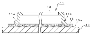
- FIGS. 6A to 6C for the mounting method of the shield case 100 according to the present invention.
- a surface mounting frame member 11 obtained by the formation process of FIGS. 3A to 5B is joined to a predetermined portion of a printed wiring board 10 (mounting board) using a solder material.
- solder material An example is given below.
- a solder material 16 ′ material is formed at a predetermined portion of the printed wiring board 10.
- a solder paste is used as the solder material 16 '.
- a printed wiring board 10 having a land pattern 10a (ground pattern) obtained by patterning a copper foil is used.
- the land pattern 10a a pattern obtained by patterning a copper foil at least on a portion facing the mounting surface of the frame member 11 is used.
- the frame member 11 shown in FIG. 6B is mounted on a predetermined portion of the land pattern 10a on which the solder material 16 'is formed.
- the mounting of the frame member 11 may be either a method using a component mounting machine or a manual mounting method.
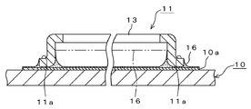
- the printed wiring board 10 including the frame member 11 mounted on the land pattern 10a via the solder material 16 ' is introduced into a reflow furnace (not shown) and subjected to a reflow process.
- the printed wiring board 10 and the frame member 11 are joined by this reflow process.
- the reflow furnace is heated and controlled according to a predetermined temperature profile.
- the target set temperature is set to 250 ° C.
- the reflow furnace conveyor speed is set to about 1.25 m / sec.
- the heating atmosphere of the printed wiring board 10 is an air atmosphere, preferably an atmosphere made of an inert gas such as nitrogen gas.
- an inert gas such as nitrogen gas.
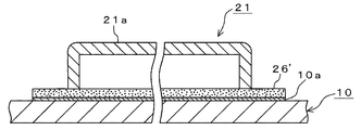
- the frame member 11 is provided with a hat-shaped (saddle-shaped) narrowed end portion 11a around the frame member 11, so that the fillet formed as shown in FIG. The outside and inside are not nearly equal. That is, the inner side is thicker and the fillet is formed.
- the throttle end portion 11 a shown in FIG. 6A is further folded to form the end portion so as to have a U-shaped cross section. Then, in addition to reinforcing the frame member 11, the U-shaped bottom is symmetrical, so the fillets formed after the frame member 11 is mounted on the printed wiring board 10 are outside and inside the frame member 11. It is formed almost evenly.
- the shield case 100 and the manufacturing method thereof after processing the frame member 11, part of which is a soldering surface for surface mounting, from the white material 1, the frame A Ni plating layer 2 and a Sn—Cu plating layer 3 having a predetermined thickness are sequentially formed on one part of the member 11 and subjected to a base treatment, and lead is applied to all parts on the Sn—Cu plating layer 3 after the base treatment.
- a solder coating layer 4 is formed by coating free molten solder, and a surface treatment layer 5 consisting of three layers as a whole is formed.
- a lead-free solder such as Cu—Ni or Sn—Ag—Cu—Sb is used.
- the solderability of the soldered portion (hereinafter referred to as the fillet portion 16) of the shield case 100 for surface mounting is further improved compared to the conventional plating method, soldering treatment such as rust prevention treatment and degreasing treatment. It can be improved.
- electronic components such as the frame member 11 excellent in bending resistance and drawing resistance, can be provided.
- solder paste alone is processed into a rectangular size (dimensional shape such as # 1005, # 1608, # 0603, etc.) similar to a chip-type electronic component at a place where a mounting failure due to insufficient solder amount may occur.
- Solid solder hereinafter referred to as chip solder
- the chip solder is a lead-free solder such as the above-mentioned Eco Solder M705, and is processed into a rectangular size similar to the chip-type electronic component. Therefore, in the existing equipment, for example, a component mounting machine such as a chip mounter, any The required amount of solder can be supplied to the location. When the chip solder is used, even if the supply amount of the solder material 16 ′ is reduced due to the miniaturization of parts or the like, it becomes possible to cope with the supply of the constant amount.
- the usage procedure of the chip solder first, since there is a possibility that a mounting failure due to an insufficient amount of solder on the printed wiring board 10 to be mounted may occur, a frequent occurrence location is specified. Next, a chip solder having a size corresponding to the dimension of the work to be mounted at the location where frequent mounting defects are identified, the land area shape, and the required supply amount is selected. Then, the mounting parameters are programmed into the chip mounter.
- a solder-coated part is a lead-free molten solder film in which a nickel film and a tin alloy plating film with a predetermined film thickness are sequentially provided on a metal part such as a shield case, and the tin alloy plating film is coated.
- the surface treatment which consists of is said.
- a shield component having a surface treatment made of a lead-free molten solder film coated on the tin alloy plating film is obtained.
- the step of processing the metal member for the solder-coated component to form the shield component for surface mounting is performed first.
- a nickel film and a tin alloy plating film were sequentially formed on the formed shield member, and after the surface treatment, the metal member was coated with molten solder and surface-treated, but this is not a limitation. .
- a nickel film and a tin alloy plating film with a predetermined film thickness are sequentially formed on a metal member as a base material for a solder coated component, and then a surface treatment is performed by coating the metal member with a molten solder.
- the surface-treated metal member may be processed to form a shield component for surface mounting.
- a shield case 200 shown in FIG. 7 constitutes an example of a solder-coated component, and electromagnetically shields an electronic component (not shown) mounted on the printed wiring board 10 in the same manner as in the first embodiment.
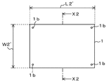
- the shield case 200 is composed of a lid member 12 and a frame member 21 reinforced with a casing. Similar to the first embodiment, the frame member 21 has a width W2 of about 38 mm, a length L2 of about 60 mm, and a height H2 of about 2 mm.
- the frame member 21 is soldered to the printed wiring board 10. As the printed wiring board 10, the one described in the first embodiment is used.
- the inside of the frame member 21 is reinforced.
- the frame member 21 has beam portions 21a and 21b intersecting with a cross.
- the beam part 21a is set wider than the width of the beam part 21b. This setting is for preventing distortion in the longitudinal direction of the frame member 21 at the beam portion 21a.
- the cross-shaped beam portions 21a and 21b divide the opening 13 described in the first embodiment into four, and the openings 13a to 13d are provided inside the frame member 21. When the lid member 12 is removed from the frame member 21, the electronic components in the four openings 13a to 13d can be inspected.
- the lower part of the outer periphery of the four openings 13a to 13d has such a shape that the cut end surface of the white material 1 is brought into contact with the land pattern 10a as it is.
- the cut end surface of the white material 1 may be bent inward or outward to provide a bent end.
- Ni plating layer 2 and the Sn—Cu plating layer 3 are successively formed and subjected to a base treatment, and then the lead-free molten solder is applied as a finishing layer on the Sn—Cu plating layer 3 after the base treatment.
- a surface treatment layer 5 composed of the coat layer 4 is formed.
- the thickness of the solder coat layer 4 is ensured to be about 18 ⁇ m to 30 ⁇ m in order to improve the wettability of the molten solder during the reflow process in the same manner as in the first embodiment.
- molten solder for example, Sn—Ag—Cu-based lead-free solder is used in the same manner as in the first embodiment.
- molten solder includes Sn-Ag, Sn-Cu, Sn-Bi, Sn-Ag-Cu-Bi, Sn-Bi-Ag (Cu), Sn A lead-free solder such as -Ag-Cu-Ni or Sn-Ag-Cu-Sb is used. Since the lid member 12 has been described in the first embodiment, the description thereof is omitted.
- FIGS. 8A to 10B an example of forming the frame member 21 will be described with reference to FIGS. 8A to 10B with respect to the manufacturing method of the shield case 200 according to the present invention.
- the western white material 1 is processed into a shield part shape having a cross structure.
- FIG. 8A is a cross-sectional view of the western white material 1 taken along line X2-X2.
- four opening portions 1b, 1b, 1b, 1b are opened at predetermined positions at the four corners of the white material 1. These opening portions 1b and the like are used as stress absorbing holes at the time of bending.
- the corner portions of the white material 1 with reference to the opening portions 1b, 1b, 1b, 1b at the four corners. Cut out (cut off) the rectangular piece using a cutting tool.
- the portions where the rectangular pieces are dropped from the corner portions of the white material 1 are referred to as notches 22a, 22b, 22c, and 22d.
- the intermediate member 21 'having the cutout portions 22a, 22b, 22c, and 22d is obtained.
- the white material 1 is set on a bending machine (not shown), and the body pressing portion and the end bending mechanism are pressed against the white material 1 to execute the bending process.
- the C-shaped portions of the opening portions 1b, 1b, 1b, and 1b remaining in the notches 22a, 22b, 22c, and 22d absorb the stress at the time of bending.
- a cap-shaped intermediate member 21a 'in which the openings 13a to 13d of the frame member 21 are not yet opened as shown in FIG. 7 is obtained.
- the lower part of the outer periphery has a shape such that the cut end surface of the white material 1 is in direct contact with the land pattern 10a. .
- FIG. 10B is a cross-sectional view of the intermediate member 21a 'taken along the arrow X3-X3.
- the Ni plating layer 2 and the Sn—Ag plating layer 3 having a predetermined film thickness are sequentially formed and the base treatment is performed. Since the ground processing at this time is the same as that in the first embodiment, the description thereof is omitted.
- a solder coat process is performed as a finishing layer on the necessary portion of the frame member 21 that has undergone the base process, as in the first embodiment. Since the solder coating process and its component supply process are the same as those in the first embodiment, the description thereof is omitted.
- FIGS. 11A to 11C an example of mounting the frame member 21 on the printed wiring board 10 will be described with respect to the mounting method of the shield case 200.
- FIG. In this example, a solder material is used for a predetermined portion of the printed wiring board 10 (mounting board) for the surface mounting frame member 21 obtained by the forming process shown in FIGS. 8A to 10B. Then, the case where it joins is mentioned as an example.
- a solder material 26 ′ material is formed at a predetermined portion of the printed wiring board 10. Since the printed wiring board 10 and the solder material 26 ′ are as described in the first embodiment, description thereof is omitted.
- the solder material 26 ' can be formed on the land pattern 10a of the printed wiring board 10, the land pattern 10a and the frame member 21 are aligned.
- the frame member 21 shown in FIG. 11B is mounted on a predetermined portion of the land pattern 10a on which the solder material 26 'is formed.
- the mounting of the frame member 21 may be either a method using a component mounting machine or a manual placement method.
- the printed wiring board 10 including the frame member 21 mounted on the land pattern 10a via the solder material 26 ' is introduced into a reflow furnace (not shown) and subjected to a reflow process.
- the printed wiring board 10 and the frame member 21 are joined by this reflow process.
- the reflow furnace is heated and controlled according to the temperature profile.
- the solder material 26 ′ on the land pattern 10 a melts and scoops the inside and outside below the frame member 21 with good wettability. Go up.
- the fillet portion 26 is formed by the rising of the molten solder. As a result, as shown in FIG. 11C, the frame member 21 and the printed wiring board 10 can be soldered satisfactorily.
- a frame member with a cross structure in the frame in which a part of the white material 1 is a soldering surface for surface mounting.
- a Ni plating layer 2 and a Sn—Ag plating layer 3 having a predetermined film thickness are sequentially formed and subjected to a ground treatment, and after the ground treatment, lead-free molten solder is coated as a finishing layer. Yes.
- Sn—Ag, Sn—Cu, Sn—Ag—Cu, Sn—Bi, Sn—Ag—Cu—Bi, Sn—Bi—Ag (Cu), Sn—Ag— Lead-free solders such as Cu—Ni and Sn—Ag—Cu—Sb are used.
- solder wettability of the fillet portion 26 of the shield case 200 for surface mounting can be further improved as compared with the conventional plating method, soldering treatment such as rust prevention treatment and degreasing treatment.
- soldering treatment such as rust prevention treatment and degreasing treatment.
- electronic components such as the frame member 21 excellent in bending resistance and drawing resistance, can be provided.
- a tuner case 300 as the third embodiment will be described with reference to FIG.
- a tuner case 300 shown in FIG. 12 constitutes an example of a solder coat component, and electromagnetically shields a tuner component (not shown) mounted on the tuner circuit board 30.
- the tuner case 300 includes a frame member 31 and a lid member 32.
- the frame member 31 has a width W3 of about 18 mm, a length L3 of about 22 mm, and a height H3 of about 2 mm.
- the frame member 31 is soldered to the tuner circuit board 30.
- a land pattern 30a is provided on the tuner circuit board 30, and the printed circuit board 10 described in the first embodiment is incorporated with a tuner circuit.
- the frame member 31 and the lid member 32 those made from the white material 1, SUS304, SUS316, SUS430 or the like are used.
- the frame member 31 is soldered to the land pattern 30a.
- the inside of the frame member 31 is reinforced flat.
- an uneven portion is provided in the direction of the end face (tree scene) of the opening 33 inside the frame member 31.
- the reason why the uneven portion is provided is to prevent the frame member 31 from being twisted or warped in the longitudinal direction or the short direction.
- the lid member 32 is removed from the frame member 31, it is possible to inspect the tuner parts in the opening portion 33 whose inside is flat-reinforced.
- the outer periphery of the opening 33 is different from the hat-shaped throttle end 11a as in the first embodiment, and the cut end surface of the white material 1 as described in the second embodiment is intact. It has a shape that comes into contact with the land pattern 30a.
- the outer periphery thereof may be the throttle end portion 11a as in the first embodiment.
- a grounding lead 32a is provided.
- the lead 32a has a leaf spring property, and when the tuner circuit board 30 on which the tuner case 300 is mounted is incorporated in a casing such as a mobile phone, the lead 32a is brought into contact with a contacted portion provided in the casing, Conductive and grounded.
- the frame member 31 of the tuner case 300 is also provided with a Ni plating layer 2 and a Sn—Cu plating layer 3 having a predetermined film thickness as shown in FIG. 2 and is melted on the Sn—Cu plating layer 3. It is comprised from the white material 1 in which the surface treatment layer 5 which consists of the solder coat layer 4 by which the solder was coated is formed.
- the solder coat layer 4 has a thickness of about 18 ⁇ m to 30 ⁇ m in order to improve the wettability of the molten solder during the reflow process.
- Sn—Ag—Cu-based lead-free solder is used for the molten solder.
- molten solder includes Sn-Ag, Sn-Cu, Sn-Bi, Sn-Ag-Cu-Bi, Sn-Bi-Ag (Cu), Sn A lead-free solder such as -Ag-Cu-Ni or Sn-Ag-Cu-Sb is used.
- the fillet portion 36 in the drawing performs heat treatment of the tuner circuit board 30 on which the frame member 31 is mounted, and the solder material on the land pattern 30a is melted so that the inside and outside of the cut end surface of the frame member 31 have good wettability. It was a crawl up and was caused by the crawl up of this molten solder.
- the frame member 31 with in-frame plane reinforcement in which a part of the white material 1 is a soldering surface for surface mounting, is processed.
- the Ni plating layer 2 and the Sn—Ag plating layer 3 are subjected to the foundation treatment, and after the foundation treatment, the lead-free molten solder is coated, so that the fillet portion 36 of the tuner case 300 for surface mounting is formed.
- the solder wettability can be further improved compared to the conventional plating method, soldering treatment such as rust prevention treatment and degreasing treatment.
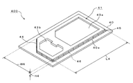
- a substrate reinforcing frame 400 as a fourth embodiment will be described with reference to FIG.
- a substrate reinforcing frame 400 shown in FIG. 13 constitutes an example of a solder-coated component, electromagnetically shields an electronic component (not shown) mounted on the light and thin circuit substrate 40, and the light and thin circuit substrate 40 itself. This prevents warping and twisting.
- the substrate reinforcing frame 400 includes a pentagonal frame member 41 having an oblique portion in part and a lid member (not shown).
- the frame member 41 has a width W4 of about 40 mm, a length L4 of about 80 mm, and a height H4 of about 2 mm.
- the frame member 41 is soldered to the light and thin circuit board 40.
- the light and thin circuit board 40 has flexibility, and the light and thin circuit board 40 is provided with a land pattern 40a.
- the frame member 41 and the lid member those made from the white material 1, stainless steel, iron, Kovar, etc. are used.
- the frame member 41 is soldered to the land pattern 40a.
- the inner side of the frame member 41 is plane-reinforced in the same manner as in the third embodiment.
- diagonal portions are provided in the direction of the end faces (tree scenes) of the two openings 43a and 43b inside the frame member 41.
- the reason why the oblique portion is provided is to prevent twisting and warping in the longitudinal direction and the short direction of the frame member 41.
- the lid member is removed from the frame member 41, the electronic components in the openings 43a and 43b whose inner surfaces are reinforced can be inspected.
- the cut end face of the frame member 31 as described in the second embodiment is different from the diaphragm end portion 11a as in the first embodiment on the outer periphery sandwiching the openings 43a and 43b. It is provided so as to contact the pattern 40a.
- the outer periphery thereof may be the throttle end portion 11a as in the first embodiment.
- the frame member 41 of the substrate reinforcing frame 400 is also provided with the Ni plating layer 2 and the Sn—Cu plating layer 3 having a predetermined film thickness as shown in FIG. 2 in order, and on the Sn—Cu plating layer 3. It is comprised from the white material 1 in which the surface treatment layer 5 which consists of the solder coat layer 4 by which the molten solder was coated is formed.
- the solder coat layer 4 has a thickness of about 18 ⁇ m to 30 ⁇ m in order to improve the wettability of the molten solder during the reflow process.
- Sn—Ag—Cu-based lead-free solder is used for the molten solder.
- molten solder includes Sn-Ag, Sn-Cu, Sn-Bi, Sn-Ag-Cu-Bi, Sn-Bi-Ag (Cu), Sn A lead-free solder such as -Ag-Cu-Ni or Sn-Ag-Cu-Sb is used.
- the fillet portion 46 in the drawing performs heat treatment of the light and thin circuit board 40 reinforced by the frame member 41, and the solder material on the land pattern 40a is melted to scoop the inner and outer sides below the frame member 41 with good wettability. This is caused by the creeping of the molten solder.
- the frame member 41 with the in-frame plane diagonal reinforcement in which a part of the white material 1 is a soldering surface for surface mounting. Since the lead-free molten solder is coated after the processing, the solder wettability of the fillet portion 46 of the substrate reinforcing frame 400 for surface mounting is determined by the conventional plating method, rust prevention treatment, degreasing treatment, etc. Compared to the soldering process, it can be further improved.
- the substrate reinforcing frame 400 such as the frame member 41 having excellent bending resistance and drawing resistance can be provided.
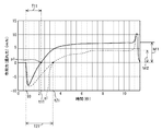
- a white material 1 (C7521R; C7701R or the like may be used) as a metal member related to the frame members 11, 21, 31, 41 is used using a meniscograph measuring device.
- the first layer was subjected to Ni plating treatment
- the second layer was subjected to Sn-Cu plating
- the third layer finishing layer
- the wet power [mN] by the molten solder was measured at every measurement elapsed time for the case and the case where the white material 1 was subjected only to the Sn plating treatment (wetting test method by the wetting balance method and the contact angle method).
- ESR250 is used as the flux
- the solder material 1 is solder-plated using Ecosolder (M705) as the molten solder.
- the immersion conditions are a measurement range of a meniscograph measuring apparatus of 20 [mN], an immersion speed of 20 mm / second, an immersion depth of 2 [mm], and an immersion holding time of 10 [seconds].
- the temperature during the reflow process is 240 ° C.
- a meniscograph was prepared based on this measurement, and the solder wettability was evaluated for the case where the white material 1 was subjected to solder coating treatment and the case where the white material 1 was subjected to Sn plating treatment.
- the solid line in the figure is the M705 treatment characteristic of the western white material 1.
- a broken line is the Sn plating processing characteristic of the white material 1. Meniscograph melts the white material 1 treated with M705 and the white material 1 treated with Sn plating from the start of heating to the completion of dipping ⁇ wet start ⁇ zero cross ⁇ wetting up ⁇ start of lifting ⁇ up of lifting. The acting force (wetting force) [mN] by the solder was measured.
- T11 is a zero crossing time from the heating start time t0 to the zero crossing time t11 of the white wood material 1 treated with M705.
- the zero crossing time T11 includes the immersion time of the molten solder, its non-wetting time, and its wetting time.
- the wetting time means the wetting speed of the molten solder treated with M705. The shorter the wetting time, the faster the wetting speed.
- a black circle mark p1 is a zero cross point of the white material 1 treated with M705.
- Fmax maximum acting force
- T21 is a zero crossing time from the heating start time t0 to the zero crossing time t21 of the white material 1 of Sn plating treatment.
- the zero crossing time T21 includes the immersion time of the molten solder, the non-wetting time thereof, and the wetting time thereof.
- the wetting time means the wetting speed of the molten solder in the Sn plating process.
- the wetting time of the Sn plating process is longer than that of the M705 process. It shows that the wetting speed of the Sn plating process is slower than that during the M705 process.
- the black circle q1 is the zero crossing point of the white material 1 subjected to Sn plating
- the wettability of the molten solder is good, and a good fillet can be formed at any soldering location that cannot be obtained with a conventional product during mounting.
- the fillet portion 16 can be formed at the portion indicated by the two-dot chain line in FIG. 6C.
- the fillet portion 26 shown in FIG. 11C, the fillet portion 36 shown in FIG. 12, the fillet portion 46 shown in FIG. 13, and the like can be formed.
- the zero crossing time T11 of the molten solder subjected to the M705 coating process is 1.34 [seconds], and the wetting time is 1.50 [seconds].
- the front of the frame member 11 is joined, but the rear of the frame member 11 is lifted from the printed wiring board 10. A satisfactory fillet could not be formed.
- the raised part is the part that is black in a strip shape in the rear photo.
- the zero crossing time T21 of the molten solder in the Sn plating process is 2.45 [seconds].
- the wetting time is 1.83 [seconds]
- the solder member is manufactured with the M705-treated frame member 11 in comparison with the Sn-plated frame member, and the solder wettability is better during the reflow process. It was proved that bonding was obtained.
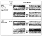
- the stainless steel SUS304 is used as the metal member related to the frame members 11, 21, 31, and 41, the ground treatment is performed in the same manner as the white material 1, and ESR250 is used as the flux.
- the solder wettability based on JISZ3198-4 also when the solder (M705) was used for the frame member made of SUS304 with the solder (M705) and when the frame member made of SUS304 was subjected only to the Sn plating treatment ( Menisco) test was conducted.
- the wettability of the molten solder is good, and a good fillet can be formed at any soldering location that cannot be obtained with a conventional product during mounting.
- the zero crossing time T11 of the molten solder subjected to the M705 coating process is 7.16 [seconds]
- the wetting time is 1.79 [seconds].
- the front of the frame member made of SUS304 is joined, but the rear of the frame member is lifted from the printed wiring board 10 and is satisfactory. A fillet could not be formed.
- the zero crossing time T21 of the molten solder in the Sn plating process is 10.00 [seconds].
- the wetting time is 0.00 [seconds].
- the present invention is extremely suitable when applied to a shield case that electromagnetically shields an electronic component mounted on a substrate or a substrate reinforcement frame that reinforces a short, small and thin substrate.
Landscapes
- Engineering & Computer Science (AREA)
- Mechanical Engineering (AREA)
- Microelectronics & Electronic Packaging (AREA)
- Shielding Devices Or Components To Electric Or Magnetic Fields (AREA)
- Chemical & Material Sciences (AREA)
- Chemical Kinetics & Catalysis (AREA)
- Electrochemistry (AREA)
- Materials Engineering (AREA)
- Metallurgy (AREA)
- Organic Chemistry (AREA)
Priority Applications (3)
| Application Number | Priority Date | Filing Date | Title |
|---|---|---|---|
| KR1020117027704A KR101970831B1 (ko) | 2009-05-22 | 2010-05-19 | 땜납 코팅 부품, 그의 제조 방법 및 그의 실장 방법 |
| KR1020167023297A KR102134500B1 (ko) | 2009-05-22 | 2010-05-19 | 땜납 코팅 부품, 그의 제조 방법 및 그의 실장 방법 |
| CN201080022520.2A CN102440091B (zh) | 2009-05-22 | 2010-05-19 | 焊料涂布元件及其制造方法、安装方法 |
Applications Claiming Priority (2)
| Application Number | Priority Date | Filing Date | Title |
|---|---|---|---|
| JP2009124716A JP5439950B2 (ja) | 2009-05-22 | 2009-05-22 | はんだコート部品、その製造方法及びその実装方法 |
| JP2009-124716 | 2009-05-22 |
Publications (1)
| Publication Number | Publication Date |
|---|---|
| WO2010134552A1 true WO2010134552A1 (ja) | 2010-11-25 |
Family
ID=43126229
Family Applications (1)
| Application Number | Title | Priority Date | Filing Date |
|---|---|---|---|
| PCT/JP2010/058466 Ceased WO2010134552A1 (ja) | 2009-05-22 | 2010-05-19 | はんだコート部品、その製造方法及びその実装方法 |
Country Status (5)
| Country | Link |
|---|---|
| JP (1) | JP5439950B2 (enExample) |
| KR (2) | KR102134500B1 (enExample) |
| CN (1) | CN102440091B (enExample) |
| TW (1) | TWI524964B (enExample) |
| WO (1) | WO2010134552A1 (enExample) |
Cited By (5)
| Publication number | Priority date | Publication date | Assignee | Title |
|---|---|---|---|---|
| CN109079270A (zh) * | 2018-10-26 | 2018-12-25 | 南通舟舰钣金有限公司 | 一种锡焊方法 |
| CN113205957A (zh) * | 2021-05-26 | 2021-08-03 | 厦门匠锐科技有限公司 | 一种骨架线圈的生产线 |
| CN115643738A (zh) * | 2021-07-19 | 2023-01-24 | 台达电子企业管理(上海)有限公司 | 功率模块和固态变压器系统 |
| EP4325568A4 (en) * | 2021-04-28 | 2024-09-11 | Senju Metal Industry Co., Ltd. | LAYERED INTERCONNECTOR, SEMICONDUCTOR HOUSING AND POWER MODULE |
| US12417876B2 (en) | 2021-07-19 | 2025-09-16 | Delta Electronics (Shanghai) Co., Ltd. | Circuit module and solid-state transformer system |
Families Citing this family (8)
| Publication number | Priority date | Publication date | Assignee | Title |
|---|---|---|---|---|
| KR101029221B1 (ko) * | 2011-01-14 | 2011-04-14 | 에프엔티주식회사 | 부분 도금층이 마련된 전자파 차단용 쉴드캔 고정클립 |
| US9391029B2 (en) | 2014-06-12 | 2016-07-12 | Kabushiki Kaisha Toshiba | Electronic device |
| DE102014110459A1 (de) * | 2014-07-24 | 2016-01-28 | Mahle International Gmbh | Wärmeübertrager |
| KR102311677B1 (ko) | 2014-08-13 | 2021-10-12 | 삼성전자주식회사 | 반도체소자 및 그 제조방법 |
| EP3737216A1 (en) * | 2015-09-18 | 2020-11-11 | Toray Industries, Inc. | Electronic device housing |
| KR102717102B1 (ko) | 2016-09-06 | 2024-10-16 | 삼성디스플레이 주식회사 | 디스플레이 장치 |
| JP6871524B1 (ja) * | 2020-03-23 | 2021-05-12 | 千住金属工業株式会社 | 積層接合材料、半導体パッケージおよびパワーモジュール |
| US11744019B2 (en) * | 2020-11-18 | 2023-08-29 | Murata Manufacturing Co., Ltd. | Component mounted on circuit board |
Citations (11)
| Publication number | Priority date | Publication date | Assignee | Title |
|---|---|---|---|---|
| JPH01289298A (ja) * | 1988-05-17 | 1989-11-21 | Alps Electric Co Ltd | シールドケースの製造方法 |
| JPH03104197A (ja) * | 1989-09-18 | 1991-05-01 | Canon Inc | シールドケース |
| JPH0563100U (ja) * | 1992-01-30 | 1993-08-20 | 京セラ株式会社 | シールドケース付電子部品 |
| JPH07147495A (ja) * | 1993-11-26 | 1995-06-06 | Nec Corp | プリント基板表面実装用シールドケース |
| JPH10117062A (ja) * | 1996-08-19 | 1998-05-06 | Sony Corp | リード部品及び高周波信号が漏洩するのを防ぐシールドケースのプリント基板への取付け方法並びに取付け装置、チップ部品、リード部品及び高周波信号が漏洩するのを防ぐシールドケースのプリント基板への取付け方法並びに取付け装置 |
| JP2001155955A (ja) * | 1999-11-30 | 2001-06-08 | Taiyo Kagaku Kogyo Kk | 外部端子電極具備電子部品及びその搭載電子用品 |
| JP2001217588A (ja) * | 2000-01-31 | 2001-08-10 | Sharp Corp | シールドケース及びそれを用いたrf通信ユニット |
| JP2002141456A (ja) * | 2000-10-30 | 2002-05-17 | Hitachi Ltd | 電子装置 |
| JP2002359312A (ja) * | 2001-05-31 | 2002-12-13 | Kinseki Ltd | 電子部品容器 |
| JP2004156147A (ja) * | 2004-03-04 | 2004-06-03 | Kobe Steel Ltd | 多極端子用錫又は錫合金めっき銅合金及びその製造方法 |
| WO2006035542A1 (ja) * | 2004-09-27 | 2006-04-06 | Murata Manufacturing Co., Ltd. | シールドケース |
Family Cites Families (5)
| Publication number | Priority date | Publication date | Assignee | Title |
|---|---|---|---|---|
| US5911356A (en) * | 1996-08-19 | 1999-06-15 | Sony Corporation | Method for attaching lead parts and shield case to printed circuit board, and method for attaching chip parts, lead parts and shield case to printed circuit board |
| JP2001007588A (ja) * | 1999-06-21 | 2001-01-12 | Alps Electric Co Ltd | 電子回路ユニット |
| JP4222015B2 (ja) * | 2002-12-04 | 2009-02-12 | 株式会社村田製作所 | 電子部品の製造方法 |
| JPWO2004070836A1 (ja) * | 2003-02-06 | 2006-06-01 | 株式会社Neomaxマテリアル | 気密封止用キャップおよびその製造方法 |
| JP2006196664A (ja) | 2005-01-13 | 2006-07-27 | Fuji Photo Film Co Ltd | 基板へのシールドケース取付構造及び携帯電話 |
-
2009
- 2009-05-22 JP JP2009124716A patent/JP5439950B2/ja active Active
-
2010
- 2010-05-19 KR KR1020167023297A patent/KR102134500B1/ko active Active
- 2010-05-19 WO PCT/JP2010/058466 patent/WO2010134552A1/ja not_active Ceased
- 2010-05-19 CN CN201080022520.2A patent/CN102440091B/zh active Active
- 2010-05-19 KR KR1020117027704A patent/KR101970831B1/ko active Active
- 2010-05-21 TW TW099116264A patent/TWI524964B/zh active
Patent Citations (11)
| Publication number | Priority date | Publication date | Assignee | Title |
|---|---|---|---|---|
| JPH01289298A (ja) * | 1988-05-17 | 1989-11-21 | Alps Electric Co Ltd | シールドケースの製造方法 |
| JPH03104197A (ja) * | 1989-09-18 | 1991-05-01 | Canon Inc | シールドケース |
| JPH0563100U (ja) * | 1992-01-30 | 1993-08-20 | 京セラ株式会社 | シールドケース付電子部品 |
| JPH07147495A (ja) * | 1993-11-26 | 1995-06-06 | Nec Corp | プリント基板表面実装用シールドケース |
| JPH10117062A (ja) * | 1996-08-19 | 1998-05-06 | Sony Corp | リード部品及び高周波信号が漏洩するのを防ぐシールドケースのプリント基板への取付け方法並びに取付け装置、チップ部品、リード部品及び高周波信号が漏洩するのを防ぐシールドケースのプリント基板への取付け方法並びに取付け装置 |
| JP2001155955A (ja) * | 1999-11-30 | 2001-06-08 | Taiyo Kagaku Kogyo Kk | 外部端子電極具備電子部品及びその搭載電子用品 |
| JP2001217588A (ja) * | 2000-01-31 | 2001-08-10 | Sharp Corp | シールドケース及びそれを用いたrf通信ユニット |
| JP2002141456A (ja) * | 2000-10-30 | 2002-05-17 | Hitachi Ltd | 電子装置 |
| JP2002359312A (ja) * | 2001-05-31 | 2002-12-13 | Kinseki Ltd | 電子部品容器 |
| JP2004156147A (ja) * | 2004-03-04 | 2004-06-03 | Kobe Steel Ltd | 多極端子用錫又は錫合金めっき銅合金及びその製造方法 |
| WO2006035542A1 (ja) * | 2004-09-27 | 2006-04-06 | Murata Manufacturing Co., Ltd. | シールドケース |
Cited By (6)
| Publication number | Priority date | Publication date | Assignee | Title |
|---|---|---|---|---|
| CN109079270A (zh) * | 2018-10-26 | 2018-12-25 | 南通舟舰钣金有限公司 | 一种锡焊方法 |
| EP4325568A4 (en) * | 2021-04-28 | 2024-09-11 | Senju Metal Industry Co., Ltd. | LAYERED INTERCONNECTOR, SEMICONDUCTOR HOUSING AND POWER MODULE |
| CN113205957A (zh) * | 2021-05-26 | 2021-08-03 | 厦门匠锐科技有限公司 | 一种骨架线圈的生产线 |
| CN113205957B (zh) * | 2021-05-26 | 2023-01-10 | 厦门匠锐科技有限公司 | 一种骨架线圈的生产线 |
| CN115643738A (zh) * | 2021-07-19 | 2023-01-24 | 台达电子企业管理(上海)有限公司 | 功率模块和固态变压器系统 |
| US12417876B2 (en) | 2021-07-19 | 2025-09-16 | Delta Electronics (Shanghai) Co., Ltd. | Circuit module and solid-state transformer system |
Also Published As
| Publication number | Publication date |
|---|---|
| CN102440091A (zh) | 2012-05-02 |
| JP2010272774A (ja) | 2010-12-02 |
| JP5439950B2 (ja) | 2014-03-12 |
| KR20160105913A (ko) | 2016-09-07 |
| TW201102208A (en) | 2011-01-16 |
| TWI524964B (zh) | 2016-03-11 |
| KR20120023002A (ko) | 2012-03-12 |
| CN102440091B (zh) | 2014-09-03 |
| KR102134500B1 (ko) | 2020-07-15 |
| KR101970831B1 (ko) | 2019-08-27 |
Similar Documents
| Publication | Publication Date | Title |
|---|---|---|
| JP5439950B2 (ja) | はんだコート部品、その製造方法及びその実装方法 | |
| CA1213073A (en) | Method of manufacturing printed wiring boards | |
| KR100680022B1 (ko) | 기판의 휨 저감 구조 및 기판의 휨 저감 방법 | |
| CN108133810B (zh) | 绕线型线圈部件以及绕线型线圈部件的制造方法 | |
| JPWO2018101405A1 (ja) | チップ型電子部品 | |
| JP5353839B2 (ja) | 電子部品 | |
| US6292083B1 (en) | Surface-mount coil | |
| US20160219721A1 (en) | Method for manufacturing solder circuit board, solder circuit board, and method for mounting electronic component | |
| US7632112B2 (en) | Electrical contact component, coaxial connector, and electrical circuit device including the same | |
| US6880243B2 (en) | Stiffener for stiffening a circuit board | |
| US20230269884A1 (en) | A manufacturing process to enhance surface mount solder pad joint formation via a laser subtractive method | |
| US7057293B2 (en) | Structure comprising a printed circuit board with electronic components mounted thereon and a method for manufacturing the same | |
| US5639014A (en) | Integral solder and plated sealing cover and method of making same | |
| US6758387B1 (en) | Solder coated material and method for its manufacture | |
| US20010047587A1 (en) | Circuit board manufacturing method, components mounting method and circuit board manufacturing device | |
| US4650548A (en) | Process for preserving the solderability of through hole plated printed circuit boards | |
| JP3827487B2 (ja) | はんだコーティング長尺材の製造方法 | |
| JP5825265B2 (ja) | プリント基板のはんだ付け方法 | |
| JP5241246B2 (ja) | めっき層及びその形成方法 | |
| KR20120068560A (ko) | 도금을 이용한 마그네슘 합금의 솔더링 방법 및 이를 이용한 이동통신 안테나용 마그네슘 합금 위상가변기 | |
| JP4371605B2 (ja) | 端子付電池 | |
| JP3801893B2 (ja) | 部材の接合方法 | |
| CN119053019A (zh) | 一种pcb板的金属屏蔽外壳焊接结构及焊接方法 | |
| CN108811367B (zh) | 一种表面贴装方法 | |
| JP2006073639A (ja) | シールドケースの実装方法,シールド構造,シールドケース実装装置 |
Legal Events
| Date | Code | Title | Description |
|---|---|---|---|
| WWE | Wipo information: entry into national phase |
Ref document number: 201080022520.2 Country of ref document: CN |
|
| 121 | Ep: the epo has been informed by wipo that ep was designated in this application |
Ref document number: 10777785 Country of ref document: EP Kind code of ref document: A1 |
|
| ENP | Entry into the national phase |
Ref document number: 20117027704 Country of ref document: KR Kind code of ref document: A |
|
| NENP | Non-entry into the national phase |
Ref country code: DE |
|
| 122 | Ep: pct application non-entry in european phase |
Ref document number: 10777785 Country of ref document: EP Kind code of ref document: A1 |