WO2010134352A1 - 有機エレクトロルミネッセンス素子 - Google Patents
有機エレクトロルミネッセンス素子 Download PDFInfo
- Publication number
- WO2010134352A1 WO2010134352A1 PCT/JP2010/003434 JP2010003434W WO2010134352A1 WO 2010134352 A1 WO2010134352 A1 WO 2010134352A1 JP 2010003434 W JP2010003434 W JP 2010003434W WO 2010134352 A1 WO2010134352 A1 WO 2010134352A1
- Authority
- WO
- WIPO (PCT)
- Prior art keywords
- group
- light emitting
- layer
- substituted
- emitting layer
- Prior art date
Links
- 0 Cc(c1c(*)c(*)c(*)c(*)c11)c(c(*)c(*)c(*)c2*)c2c1[Al] Chemical compound Cc(c1c(*)c(*)c(*)c(*)c11)c(c(*)c(*)c(*)c2*)c2c1[Al] 0.000 description 2
Images


Classifications
-
- H—ELECTRICITY
- H10—SEMICONDUCTOR DEVICES; ELECTRIC SOLID-STATE DEVICES NOT OTHERWISE PROVIDED FOR
- H10K—ORGANIC ELECTRIC SOLID-STATE DEVICES
- H10K50/00—Organic light-emitting devices
- H10K50/10—OLEDs or polymer light-emitting diodes [PLED]
- H10K50/11—OLEDs or polymer light-emitting diodes [PLED] characterised by the electroluminescent [EL] layers
-
- C—CHEMISTRY; METALLURGY
- C09—DYES; PAINTS; POLISHES; NATURAL RESINS; ADHESIVES; COMPOSITIONS NOT OTHERWISE PROVIDED FOR; APPLICATIONS OF MATERIALS NOT OTHERWISE PROVIDED FOR
- C09B—ORGANIC DYES OR CLOSELY-RELATED COMPOUNDS FOR PRODUCING DYES, e.g. PIGMENTS; MORDANTS; LAKES
- C09B57/00—Other synthetic dyes of known constitution
- C09B57/001—Pyrene dyes
-
- C—CHEMISTRY; METALLURGY
- C09—DYES; PAINTS; POLISHES; NATURAL RESINS; ADHESIVES; COMPOSITIONS NOT OTHERWISE PROVIDED FOR; APPLICATIONS OF MATERIALS NOT OTHERWISE PROVIDED FOR
- C09B—ORGANIC DYES OR CLOSELY-RELATED COMPOUNDS FOR PRODUCING DYES, e.g. PIGMENTS; MORDANTS; LAKES
- C09B57/00—Other synthetic dyes of known constitution
- C09B57/008—Triarylamine dyes containing no other chromophores
-
- C—CHEMISTRY; METALLURGY
- C09—DYES; PAINTS; POLISHES; NATURAL RESINS; ADHESIVES; COMPOSITIONS NOT OTHERWISE PROVIDED FOR; APPLICATIONS OF MATERIALS NOT OTHERWISE PROVIDED FOR
- C09B—ORGANIC DYES OR CLOSELY-RELATED COMPOUNDS FOR PRODUCING DYES, e.g. PIGMENTS; MORDANTS; LAKES
- C09B69/00—Dyes not provided for by a single group of this subclass
- C09B69/008—Dyes containing a substituent, which contains a silicium atom
-
- H—ELECTRICITY
- H05—ELECTRIC TECHNIQUES NOT OTHERWISE PROVIDED FOR
- H05B—ELECTRIC HEATING; ELECTRIC LIGHT SOURCES NOT OTHERWISE PROVIDED FOR; CIRCUIT ARRANGEMENTS FOR ELECTRIC LIGHT SOURCES, IN GENERAL
- H05B33/00—Electroluminescent light sources
- H05B33/10—Apparatus or processes specially adapted to the manufacture of electroluminescent light sources
-
- H—ELECTRICITY
- H05—ELECTRIC TECHNIQUES NOT OTHERWISE PROVIDED FOR
- H05B—ELECTRIC HEATING; ELECTRIC LIGHT SOURCES NOT OTHERWISE PROVIDED FOR; CIRCUIT ARRANGEMENTS FOR ELECTRIC LIGHT SOURCES, IN GENERAL
- H05B33/00—Electroluminescent light sources
- H05B33/12—Light sources with substantially two-dimensional radiating surfaces
- H05B33/14—Light sources with substantially two-dimensional radiating surfaces characterised by the chemical or physical composition or the arrangement of the electroluminescent material, or by the simultaneous addition of the electroluminescent material in or onto the light source
-
- H—ELECTRICITY
- H10—SEMICONDUCTOR DEVICES; ELECTRIC SOLID-STATE DEVICES NOT OTHERWISE PROVIDED FOR
- H10K—ORGANIC ELECTRIC SOLID-STATE DEVICES
- H10K85/00—Organic materials used in the body or electrodes of devices covered by this subclass
- H10K85/60—Organic compounds having low molecular weight
- H10K85/615—Polycyclic condensed aromatic hydrocarbons, e.g. anthracene
- H10K85/622—Polycyclic condensed aromatic hydrocarbons, e.g. anthracene containing four rings, e.g. pyrene
-
- H—ELECTRICITY
- H10—SEMICONDUCTOR DEVICES; ELECTRIC SOLID-STATE DEVICES NOT OTHERWISE PROVIDED FOR
- H10K—ORGANIC ELECTRIC SOLID-STATE DEVICES
- H10K85/00—Organic materials used in the body or electrodes of devices covered by this subclass
- H10K85/60—Organic compounds having low molecular weight
- H10K85/615—Polycyclic condensed aromatic hydrocarbons, e.g. anthracene
- H10K85/626—Polycyclic condensed aromatic hydrocarbons, e.g. anthracene containing more than one polycyclic condensed aromatic rings, e.g. bis-anthracene
-
- H—ELECTRICITY
- H10—SEMICONDUCTOR DEVICES; ELECTRIC SOLID-STATE DEVICES NOT OTHERWISE PROVIDED FOR
- H10K—ORGANIC ELECTRIC SOLID-STATE DEVICES
- H10K85/00—Organic materials used in the body or electrodes of devices covered by this subclass
- H10K85/60—Organic compounds having low molecular weight
- H10K85/631—Amine compounds having at least two aryl rest on at least one amine-nitrogen atom, e.g. triphenylamine
- H10K85/633—Amine compounds having at least two aryl rest on at least one amine-nitrogen atom, e.g. triphenylamine comprising polycyclic condensed aromatic hydrocarbons as substituents on the nitrogen atom
-
- H—ELECTRICITY
- H10—SEMICONDUCTOR DEVICES; ELECTRIC SOLID-STATE DEVICES NOT OTHERWISE PROVIDED FOR
- H10K—ORGANIC ELECTRIC SOLID-STATE DEVICES
- H10K2101/00—Properties of the organic materials covered by group H10K85/00
- H10K2101/10—Triplet emission
-
- H—ELECTRICITY
- H10—SEMICONDUCTOR DEVICES; ELECTRIC SOLID-STATE DEVICES NOT OTHERWISE PROVIDED FOR
- H10K—ORGANIC ELECTRIC SOLID-STATE DEVICES
- H10K2101/00—Properties of the organic materials covered by group H10K85/00
- H10K2101/30—Highest occupied molecular orbital [HOMO], lowest unoccupied molecular orbital [LUMO] or Fermi energy values
-
- H—ELECTRICITY
- H10—SEMICONDUCTOR DEVICES; ELECTRIC SOLID-STATE DEVICES NOT OTHERWISE PROVIDED FOR
- H10K—ORGANIC ELECTRIC SOLID-STATE DEVICES
- H10K85/00—Organic materials used in the body or electrodes of devices covered by this subclass
- H10K85/60—Organic compounds having low molecular weight
Definitions
- the present invention relates to an organic electroluminescence (EL) element, particularly a highly efficient organic EL element.
- EL organic electroluminescence
- organic EL elements When organic EL elements are classified according to their light emission principles, they can be divided into two types: fluorescent and phosphorescent types.
- fluorescent and phosphorescent types When a voltage is applied to the organic EL element, holes are injected from the anode and electrons are injected from the cathode, and these recombine in the light emitting layer to form excitons.
- electrons According to the statistical rule of electron spin, singlet excitons and triplet excitons are generated at a ratio of 25%: 75%. Since the fluorescence type uses light emitted from singlet excitons, the internal quantum efficiency was said to be 25%.
- a fluorescent element using a fluorescent material has recently been developed with a long-life technology and is being applied to a full-color display such as a mobile phone or a television. However, high efficiency has been a problem.
- Non-Patent Document 1 a non-doped element using an anthracene compound as a host material is analyzed, and as a mechanism, singlet excitons are generated by collisional fusion of two triplet excitons. Fluorescence emission is increasing.
- Non-Patent Document 1 only discloses that an increase in fluorescence emission is confirmed by collisional fusion of triplet excitons in a non-doped element composed of only a host material. The increase was as low as 3-6%.
- Non-Patent Document 2 reports that the blue quantum element has an internal quantum efficiency of 28.5%, which exceeds the conventional theoretical limit of 25%. However, no technical means for exceeding 25% has been disclosed, and further higher efficiency has been demanded from the viewpoint of practical use of a full-color organic EL television.
- Patent Document 1 Another example using triplet excitons in a fluorescent element is disclosed in Patent Document 1.
- the lowest triplet excited state (T1) is lower than the lowest singlet excited state (S1), but the higher triplet excited state (T2) may be higher than S1.
- the external quantum efficiency is about 6% (when the light extraction efficiency is 25%, the internal quantum efficiency is 24%), which does not exceed the limit value of 25% that has been conventionally known.
- the mechanism here is due to intersystem crossing from a triplet excited state to a singlet excited state in one molecule, and the two triplet excitons disclosed in Non-Patent Document 1 The singlet generation phenomenon due to the collision has not occurred.
- phenanthroline derivatives such as BCP (Bathocuproin) and BPhen are used for the hole blocking layer in the fluorescent element, thereby increasing the density of holes at the interface between the hole blocking layer and the light emitting layer, and efficiently. Techniques for causing recombination are disclosed.
- phenanthroline derivatives such as BCP (basocuproin) and BPhen are vulnerable to holes, have poor oxidation durability, and have insufficient performance from the viewpoint of extending the lifetime of the device.
- Patent Documents 4 and 5 disclose examples in which an aromatic compound such as an anthracene derivative is used as a material for an electron transport layer in contact with a light emitting layer in a fluorescent element.
- an aromatic compound such as an anthracene derivative
- the triplet energy of the electron transport layer normally designed in so-called phosphorescent devices.
- the triplet energy of the electron transport layer is smaller than the triplet energy of the light-emitting layer, so that triplet excitons generated in the light-emitting layer are actually transported by electrons. It has been diffused to the layer and then undergoes a thermal deactivation process, and it has been difficult to exceed 25%, which is the theoretical limit value of conventional fluorescence.
- Patent Document 6 discloses a device using a fluoranthene dopant exhibiting long-life and high-efficiency blue light emission, but it is not necessarily high-efficiency.
- the phosphorescent type uses light emitted directly from triplet excitons. Since singlet exciton energy is also converted into triplet exciton by spin conversion inside the light emitting molecule, it is expected that an internal light emission efficiency of nearly 100% can be obtained in principle. Therefore, since a phosphorescent light emitting device using an Ir complex was announced by Forrest et al. In 2000, a phosphorescent light emitting device has attracted attention as a technique for improving the efficiency of organic EL devices. However, although red phosphorescent devices have reached the practical application range, green and blue phosphorescent devices have a shorter lifetime than fluorescent-type devices, and in particular, blue phosphorescence has insufficient color purity and luminous efficiency. The current situation is that it has not been put into practical use.
- Triplet-Triplet Fusion TTF phenomenon
- a material having a large triplet energy is used as a layer (referred to as a barrier layer in the present invention) whose term energy is in a specific relationship and adjacent to the cathode side interface of the light emitting layer, triplet excitons are It was confined in the light emitting layer, and the TTF phenomenon was efficiently caused to realize high efficiency and long life of the fluorescent element.
- JP-T-2002-525808 discloses a technique for improving efficiency by providing a barrier layer made of BCP (basocuproin) which is a phenanthroline derivative so as to be adjacent to the light emitting layer, and confining holes and excitons. Yes.
- BCP basic polypeptide
- a specific aromatic ring compound is used for a hole blocking layer to achieve high efficiency and long life.
- TTA triplet-triplet annihilation
- the following organic EL elements are provided.
- An anode, a light emitting layer, a barrier layer, an electron injection layer, and a cathode are provided in this order,
- the light emitting layer includes a host and a dopant exhibiting fluorescence emission having a main peak wavelength of 550 nm or less,
- the affinity Ad of the dopant is smaller than the affinity Ah of the host;
- a triplet energy E T d of the dopant is greater than a triplet energy E T h of the host;
- a hole transport zone is provided between the anode and the light emitting layer, Wherein the hole transport in the band, the hole-transporting layer is provided adjacent to the light-emitting layer, the triplet energy E T ho of the hole-transporting layer is larger than E T h, 2.
- the organic electroluminescence device according to any one of 1 to 3, wherein the material constituting the electron injection layer is the same as the material constituting the barrier layer, and the electron injection layer is doped with a donor. 6). 6. The organic electroluminescence device according to any one of 1 to 5, wherein the dopant is a material selected from pyrene derivatives, aminoanthracene derivatives, aminochrysene derivatives, and aminopyrene derivatives. 7). 7. The organic electroluminescence according to any one of 1 to 6, wherein an electron mobility of a material constituting the barrier layer is 10 ⁇ 6 cm 2 / Vs or more in an electric field strength of 0.04 to 0.5 MV / cm. element. 8). 8.
- the organic electroluminescence device according to any one of 1 to 10, wherein the dopant is a compound containing no double bond other than a cyclic structure.
- the light emitting layer includes a host and a dopant exhibiting fluorescence emission having a main peak wavelength of 550 nm or less,
- the affinity level Ad of the dopant is smaller than the affinity level Ah of the host;
- a triplet energy E T d of the dopant is greater than a triplet energy E T h of the host;
- a barrier layer is provided adjacent to the light emitting layer, and the triplet energy E T b of the material forming the barrier layer is larger than E T h , and the current efficiency (unit: cd / A) ),
- the emission intensity derived from singlet excitons generated by collision of triplet excitons generated in the light emitting layer is 30% or more of the total emission intensity.
- Electroluminescence element 13. The organic electroluminescence device according to any one of 1 to 12, wherein two or more light emitting layers are provided between the anode and the cathode, and an intermediate layer is provided between the two light emitting layers. 14 13. The organic electroluminescence device according to any one of 1 to 12, comprising a plurality of light emitting layers between the anode and the cathode, and a charge barrier layer between the first light emitting layer and the second light emitting layer.
- the TTF phenomenon is efficiently caused inside the light emitting layer, and as a result, a highly efficient device that greatly exceeds the internal quantum efficiency of 25%, which is said to be the limit value of the conventional fluorescent device, can be realized.
- Example TB1, TB2, ET it is a diagram illustrating BCP, BPhen, the electron mobility of Alq 3. It is a figure which shows the transient EL waveform of Example 1 and Comparative Example 1. It is a figure which shows the TTF ratio of Example 1 and Comparative Example 1.
- the present invention utilizes the TTF phenomenon.
- the TTF phenomenon will be described below. Holes and electrons injected from the anode and cathode recombine in the light emitting layer to generate excitons.
- the spin state has a ratio of 25% for singlet excitons and 75% for triplet excitons, as is conventionally known.
- a conventionally known fluorescent element light is emitted when 25% of singlet excitons are relaxed to the ground state, but the remaining 75% of triplet excitons are thermally emitted without emitting light. It returns to the ground state through the deactivation process. Therefore, the theoretical limit value of the internal quantum efficiency of the conventional fluorescent element was said to be 25%.
- TTF ratio TTF-derived emission ratio
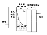
- FIG. 1 is a schematic configuration diagram of an organic EL element showing an example of the first embodiment of the present invention.
- FIG. 2A schematically shows the lowest excited singlet energy level and the lowest excited triplet energy level of each layer.
- the triplet energy means a difference between the energy in the lowest excited triplet state and the energy in the ground state
- the singlet energy (sometimes referred to as an energy gap) is the energy in the lowest excited singlet state and the ground state. This is the difference in energy.
- the organic EL element shown in FIG. 1 is laminated in order of the hole transport zone 50, the light emitting layer 20, the electron transport zone 30, and the cathode 40 in order from the anode 10.
- a hole transport zone 50 is preferably provided between the anode 10 and the light emitting layer 20.
- the term “barrier layer” refers to a layer having a barrier function against triplet energy. Therefore, the hole barrier layer and the charge barrier layer have different functions.
- the light-emitting layer is formed of a host and a dopant that emits fluorescence having a main peak wavelength of 550 nm or less (hereinafter also referred to as a fluorescent light-emitting dopant having a main peak wavelength of 550 nm or less).
- the peak wavelength of the emission spectrum at which the emission intensity in the emission spectrum measured in a toluene solution of ⁇ 5 to 10 ⁇ 6 mol / liter is maximum).
- the main peak wavelength of 550 nm corresponds to about green light emission, and in this wavelength region, it is desired to improve the light emission efficiency of the fluorescent light emitting element using the TTF phenomenon.
- a fluorescent light emitting device that emits blue light of 480 nm or less, higher luminous efficiency can be expected.
- phosphorescent light-emitting devices with high internal quantum efficiency are already in practical use, so that it is not desired to improve the light emission efficiency as fluorescent devices.
- FIG. 2A holes injected from the anode are injected into the light emitting layer through the hole transport band, and electrons injected from the cathode are injected into the light emitting layer through the electron transport band. Thereafter, holes and electrons are recombined in the light emitting layer, and singlet excitons and triplet excitons are generated.
- the triplet excitons collide with each other on the host efficiently by the TTF phenomenon without the host triplet excitons moving to the dopant, thereby generating singlet excitons. Furthermore, since the singlet energy E S d of the dopant is smaller than the singlet energy E S h of the host, singlet excitons generated by the TTF phenomenon transfer energy from the host to the dopant and contribute to the fluorescence emission of the dopant. To do. Originally, in a dopant used in a fluorescent element, a transition from an excited triplet state to a ground state is forbidden. In such a transition, the triplet exciton does not undergo optical energy deactivation and is thermally depleted. It was alive. However, by making the relationship between the triplet energy of the host and the dopant as described above, singlet excitons are efficiently generated by collision with each other before the triplet excitons are thermally deactivated, and the luminous efficiency is increased. Will improve.
- the electron transport zone has a barrier layer in a portion adjacent to the light emitting layer.
- the barrier layer prevents the triplet excitons generated in the light-emitting layer from diffusing into the electron transport band, and traps the triplet excitons in the light-emitting layer. It has a function of increasing the density and causing the TTF phenomenon efficiently.
- the triplet energy E T b of the barrier layer is preferably larger than E T h and further larger than E T d .
- the barrier layer prevents the triplet excitons from diffusing into the electron transport band, the host triplet excitons efficiently become singlet excitons in the light-emitting layer, and the singlet excitons are It moves onto the dopant to deactivate the optical energy.
- a hydrocarbon aromatic ring compound is preferably selected. More preferably, a polycyclic aromatic compound is selected. Since these materials have hole resistance, they hardly deteriorate and have a long life.
- an electron injection layer that facilitates electron injection from the cathode is preferably provided between the barrier layer and the cathode.
- Specific examples include those obtained by laminating a normal electron transport material and an alkali metal compound, an alkali metal or an alkali metal complex, or a material which forms a barrier layer, and a donor represented by an alkali metal compound, an alkali metal or an alkali metal complex. Can be used.
- the affinity of the host and the dopant is described as Ah and Ad, respectively, and the ionization potential of the host and the dopant is described as Ih and Id, respectively.
- a dopant satisfying the relationship Ah> Ad is selected.
- the dopant used in the present invention is a dopant exhibiting fluorescence emission with a main peak wavelength of 550 nm or less (hereinafter also referred to as a fluorescence emitting dopant with a main peak wavelength of 550 nm or less), and has a relatively large energy gap. Therefore, when the relationship of Ah> Ad is satisfied, the relationship of Ih> Id is satisfied at the same time, so that the dopant easily functions as a hole trap.
- FIG. 3 shows the relationship between the host and the dopant Ip-Af in the light emitting layer at this time.
- the dopant has a hole trapping property, and triplet excitons are generated not only on the host molecule but also directly on the dopant molecule. More triplet excitons are generated on the dopant. If E T h ⁇ E T d as in the present invention, the triplet exciton energy on the dopant molecule is transferred to the host molecule by Dexter energy transfer, resulting in all triplet excitations. Children gather on the host. As a result, the TTF phenomenon occurs efficiently.
- the dopant has a hole trapping property
- holes injected into the light emitting layer from the hole transport zone are trapped by the dopant, so that recombination frequently occurs on the anode side in the light emitting layer.
- the triplet energy of the hole transport material used in the conventionally known hole transport band is often larger than the triplet energy of the host in many cases, and diffusion of triplet excitons on the hole side is not a problem. There wasn't.
- the triplet energy of the barrier layer is increased. By doing so, high efficiency can be achieved.
- the recombination region includes carrier mobility, ionization potential, affinity, and film thickness in the hole transport band and electron transport band.
- the thickness of the electron transport zone is larger than the hole transport zone, the amount of electrons injected into the light emitting layer is relatively small, and as a result, the recombination region is biased toward the electron transport zone.
- the TTF phenomenon can be caused more effectively.
- the host and dopant satisfying the affinity relationship as described above can be selected from, for example, the following compounds (see Japanese Patent Application No. 2008-212102).
- the host is an anthracene derivative, a polycyclic aromatic skeleton-containing compound, preferably an anthracene derivative.
- the dopant is a pyrene derivative, aminoanthracene derivative, aminochrysene derivative, or aminopyrene derivative.
- a preferred example of the combination of host and dopant is a combination of an anthracene derivative as a host and at least one dopant selected from a pyrene derivative, aminoanthracene derivative, aminochrysene derivative, and aminopyrene derivative as a dopant.
- aminoanthracene derivatives include the following compounds.
- a 1 and A 2 each independently represents a substituted or unsubstituted aliphatic hydrocarbon group having 1 to 6 ring carbon atoms, a substituted or unsubstituted aromatic hydrocarbon group having 6 to 20 carbon atoms, nitrogen, sulfur, or A substituted or unsubstituted C5-C19 heteroaromatic hydrocarbon group containing an oxygen atom.
- a 3 is independently a substituted or unsubstituted C1-C6 aliphatic hydrocarbon group, a substituted or unsubstituted C6-C20 aromatic hydrocarbon group, or a substituted or unsubstituted group containing a nitrogen, sulfur or oxygen atom A C5-C19 heteroaromatic hydrocarbon group or a hydrogen atom.
- aminochrysene derivatives include the following compounds.
- X 1-10 is each H or a substituent, and Y 1 and Y 2 are each a substituent.
- X 1-10 is H.
- Y 1 and Y 2 are substituted (preferably substituted with C 1-6 alkyl) or unsubstituted C 6-30 aromatic rings (preferably C 6-10 or phenyl).
- X 1-10 is H or a substituent, respectively, provided that X 3 and X 8 or X 2 and X 7 are each —NY 1 Y 2 (Y 1 and Y 2 are substituents).
- X 3 and X 8 are each —NY 1 Y 2
- X 2,4,5,7,9,10 is H and X 1
- X 6 are hydrogen, alkyl or cycloalkyl .
- X 1,3-6,8-10 is H when X 2 and X 7 are each —NY 1 Y 2 .
- Y 1 and Y 2 are substituted (eg C 1-6 alkyl) or unsubstituted aromatic rings (eg phenyl, naphthyl).
- the anthracene derivative is preferably a compound represented by the following formula (10).
- Ar 11 and Ar 12 are each independently a substituted or unsubstituted aryl group having 6 to 50 ring carbon atoms or a heterocyclic group having 5 to 50 ring atoms
- R 1 to R 8 each independently represents a hydrogen atom, a substituted or unsubstituted aryl group having 6 to 50 ring carbon atoms, a substituted or unsubstituted heterocyclic group having 5 to 50 ring atoms, substituted or unsubstituted Substituted alkyl group having 1 to 50 carbon atoms, substituted or unsubstituted cycloalkyl group having 3 to 50 ring carbon atoms, substituted or unsubstituted alkoxy group having 1 to 50 carbon atoms, substituted or unsubstituted carbon number 7 -50 aralkyl group, substituted or unsubstituted aryloxy group having 6 to 50 ring carbon atoms, substituted or unsubstituted arylthi
- the anthracene derivative according to the present invention is preferably any of the following anthracene derivatives (A), (B), and (C), and is selected depending on the configuration of the organic EL element to be applied and the required characteristics.
- Ar 11 and Ar 12 in Formula (10) are each independently a substituted or unsubstituted condensed aryl group having 10 to 50 ring carbon atoms.
- the anthracene derivative can be classified into a case where Ar 11 and Ar 12 are the same substituted or unsubstituted condensed aryl group and a case where they are different substituted or unsubstituted condensed aryl groups.
- anthracene derivatives represented by the following formulas (2-1) to (2-3), and anthracene derivatives in which Ar 11 and Ar 12 in formula (10) are different substituted or unsubstituted condensed aryl groups Is mentioned.
- Ar 11 and Ar 12 are substituted or unsubstituted 9-phenanthrenyl groups.
- R 1 to R 8 are the same as above, R 11 is a hydrogen atom, a substituted or unsubstituted aryl group having 6 to 50 ring carbon atoms, a substituted or unsubstituted heterocyclic group having 5 to 50 ring atoms, a substituted or unsubstituted carbon group having 1 to 50 carbon atoms.
- a silyl group, a carboxyl group, a halogen atom, a cyano group, a nitro group and a hydroxyl group, a is an integer of 0 to 9.
- a is an integer of 2 or more, a plurality of R 11 s may be the same or different on condition that two substituted or
- Ar 11 and Ar 12 in the formula (10) are substituted or unsubstituted 2-naphthyl groups.
- R 1 to R 8 and R 11 are the same as above, b is an integer of 1 to 7.
- b is an integer of 2 or more, a plurality of R 11 may be the same or different on condition that two substituted or unsubstituted 2-naphthyl groups are the same.
- Ar 11 and Ar 12 in the formula (10) are substituted or unsubstituted 1-naphthyl groups.
- R 1 to R 8 , R 11 and b are the same as described above.
- b is an integer of 2 or more, a plurality of R 11 are two substituted or unsubstituted. Each may be the same or different, provided that the 1-naphthyl groups are the same.
- Ar 11 and Ar 12 in formula (10) are different substituted or unsubstituted condensed aryl groups
- Ar 11 and Ar 12 are substituted or unsubstituted 9-phenanthrenyl group
- substituted or unsubstituted 1 -It is preferably either a naphthyl group or a substituted or unsubstituted 2-naphthyl group.
- Ar 11 is a 1-naphthyl group and Ar 12 is a 2-naphthyl group
- Ar 11 is a 1-naphthyl group and Ar 12 is a 9-phenanthryl group
- Ar 11 is 2- This is the case where the naphthyl group and Ar 12 are a 9-phenanthryl group.
- anthracene derivative (B) In the anthracene derivative, one of Ar 11 and Ar 12 in formula (10) is a substituted or unsubstituted phenyl group, and the other is a substituted or unsubstituted condensed aryl group having 10 to 50 ring carbon atoms. .
- Specific examples of the anthracene derivative include anthracene derivatives represented by the following formulas (2-4) and (2-5).
- Ar 11 in the formula (10) is a substituted or unsubstituted 1-naphthyl group
- Ar 12 is a substituted or unsubstituted phenyl group.
- Ar 6 represents a substituted or unsubstituted aryl group having 6 to 50 ring carbon atoms, a substituted or unsubstituted alkyl group having 1 to 50 carbon atoms, a substituted or unsubstituted cycloalkyl group having 3 to 50 ring carbon atoms, Substituted or unsubstituted aralkyl group having 7 to 50 carbon atoms, substituted or unsubstituted heterocyclic group having 5 to 50 ring atoms, 9,9-dimethylfluoren-1-yl group, 9,9-dimethylfluorene- 2-yl group, 9,9-dimethylfluoren-3-yl group, 9,9-dimethylfluoren-4-yl group, dibenzofuran-1-yl group, dibenzofuran-2-yl group, dibenzofuran-3-yl group, Or a di
- Ar 6 may form a ring such as a substituted or unsubstituted fluorenyl group or a substituted or unsubstituted dibenzofuranyl group together with a benzene ring to which Ar 6 is bonded.
- b is an integer of 2 or more, the plurality of R 11 may be the same or different.
- Ar 11 in the formula (10) is a substituted or unsubstituted 2-naphthyl group
- Ar 12 is a substituted or unsubstituted phenyl group.
- R 1 to R 8 , R 11 and b are the same as above, Ar 7 is a substituted or unsubstituted aryl group having 6 to 50 ring carbon atoms, a substituted or unsubstituted heterocyclic group having 5 to 50 ring atoms, or a substituted or unsubstituted alkyl group having 1 to 50 carbon atoms.
- Ar 7 may form a ring such as a substituted or unsubstituted fluorenyl group or a substituted or unsubstituted dibenzofuranyl group together with a benzene ring to which Ar 7 is bonded.
- b is an integer of 2 or more, the plurality of R 11 may be the same or different.
- the anthracene derivative is represented by the following formula (2-6), specifically, any one of the following formulas (2-6-1), (2-6-2), and (2-6-3) It is preferable that it is a derivative represented.
- Ar 5 is a substituted or unsubstituted aryl group having 6 to 50 ring carbon atoms, a substituted or unsubstituted alkyl group having 1 to 50 carbon atoms, a substituted or unsubstituted cycloalkyl group having 3 to 50 ring carbon atoms, A substituted or unsubstituted aralkyl group having 7 to 50 carbon atoms, or a substituted or unsubstituted heterocyclic group having 5 to 50 ring atoms, and Ar 5 and Ar 6 are independently selected. )
- R 1 to R 8 are as defined above.
- R 1 to R 8 are as defined above.
- Ar 8 is a substituted or unsubstituted condensed aryl group having 10 to 20 ring carbon atoms.
- R 1 to R 8 are the same as in the formula (10).
- Ar 5a and Ar 6a are each independently a substituted or unsubstituted condensed aryl group having 10 to 20 ring carbon atoms.
- Examples of the substituted or unsubstituted aryl group having 6 to 50 ring carbon atoms of R 1 to R 8 , R 11 , Ar 5 to Ar 7 , Ar 11 and Ar 12 include a phenyl group, a 1-naphthyl group and a 2-naphthyl group.
- an unsubstituted phenyl group A substituted phenyl group and a substituted or unsubstituted aryl group having 10 to 14 ring carbon atoms (for example, 1-naphthyl group, 2-naphthyl group, 9-phenanthryl group), substituted or unsubstituted fluorenyl group (2-fluorenyl group) Base) And a substituted or unsubstituted pyrenyl group (1-pyrenyl group, 2-pyrenyl group, 4-pyrenyl group).
- Examples of the substituted or unsubstituted condensed aryl group having 10 to 20 ring carbon atoms of Ar 5a , Ar 6a and Ar 8 include 1-naphthyl group, 2-naphthyl group, 1-anthryl group, 2-anthryl group, 9-anthryl group, 1-phenanthryl group, 2-phenanthryl group, 3-phenanthryl group, 4-phenanthryl group, 9-phenanthryl group, 1-naphthacenyl group, 2-naphthacenyl group, 9-naphthacenyl group, 1-pyrenyl group, Examples include 2-pyrenyl group, 4-pyrenyl group, 2-fluorenyl group and the like. In particular, a 1-naphthyl group, a 2-naphthyl group, a 9-phenanthryl group, and a fluorenyl group (2-fluorenyl group) are preferable.
- Examples of the substituted or unsubstituted heterocyclic group having 5 to 50 ring atoms of R 1 to R 8 , R 11 , Ar 5 to Ar 7 , Ar 11 and Ar 12 include a 1-pyrrolyl group, a 2-pyrrolyl group, 3-pyrrolyl, pyrazinyl, 2-pyridinyl, 3-pyridinyl, 4-pyridinyl, 1-indolyl, 2-indolyl, 3-indolyl, 4-indolyl, 5-indolyl, 6- Indolyl group, 7-indolyl group, 1-isoindolyl group, 2-isoindolyl group, 3-isoindolyl group, 4-isoindolyl group, 5-isoindolyl group, 6-isoindolyl group, 7-isoindolyl group, 2-furyl group, 3- Furyl group, 2-benzofuranyl group, 3-benzofuranyl group, 4-benzofur
- 1-dibenzofuranyl group 2-dibenzofuranyl group, 3-dibenzofuranyl group, 4-dibenzofuranyl group, 1-dibenzothiophenyl group, 2-dibenzothiophenyl group, 3-dibenzothiophenyl group Group, 4-dibenzothiophenyl group, 1-carbazolyl group, 2-carbazolyl group, 3-carbazolyl group, 4-carbazolyl group, 9-carbazolyl group.
- Examples of the substituted or unsubstituted alkyl group having 1 to 50 carbon atoms of R 1 to R 8 , R 11 and Ar 5 to Ar 7 include methyl group, ethyl group, propyl group, isopropyl group, n-butyl group, s- Butyl, isobutyl, t-butyl, n-pentyl, n-hexyl, n-heptyl, n-octyl, hydroxymethyl, 1-hydroxyethyl, 2-hydroxyethyl, 2-hydroxy Isobutyl group, 1,2-dihydroxyethyl group, 1,3-dihydroxyisopropyl group, 2,3-dihydroxy-t-butyl group, 1,2,3-trihydroxypropyl group, chloromethyl group, 1-chloroethyl group, 2-chloroethyl group, 2-chloroisobutyl group, 1,2-dichloroethyl group, 1,3-d
- Examples of the substituted or unsubstituted cycloalkyl group having 3 to 50 ring carbon atoms of the substituents R 1 to R 8 , R 11 and Ar 5 to Ar 7 include a cyclopropyl group, a cyclobutyl group, a cyclopentyl group, a cyclohexyl group, Examples include 4-methylcyclohexyl group, 1-adamantyl group, 2-adamantyl group, 1-norbornyl group, 2-norbornyl group and the like. Preferably, they are a cyclopentyl group and a cyclohexyl group.
- the substituted or unsubstituted alkoxy group having 1 to 50 carbon atoms of R 1 to R 8 and R 11 is a group represented by —OZ, and Z is the substituted or unsubstituted carbon number of R 1 to R 8. Selected from 1 to 50 alkyl groups.
- R 1 to R 8 , R 11 and Ar 5 to Ar 7 as a substituted or unsubstituted aralkyl group having 7 to 50 carbon atoms (the aryl moiety has 6 to 49 carbon atoms and the alkyl moiety has 1 to 44 carbon atoms) are benzyl group, 1-phenylethyl group, 2-phenylethyl group, 1-phenylisopropyl group, 2-phenylisopropyl group, phenyl-t-butyl group, ⁇ -naphthylmethyl group, 1- ⁇ -naphthylethyl group, 2- ⁇ -naphthylethyl group, 1- ⁇ -naphthylisopropyl group, 2- ⁇ -naphthylisopropyl group, ⁇ -naphthylmethyl group, 1- ⁇ -naphthylethyl group, 2- ⁇ -naphthylethyl group, 1- ⁇ -
- the substituted or unsubstituted aryloxy group and arylthio group having 6 to 50 ring carbon atoms of R 1 to R 8 and R 11 are represented by —OY and —SY, respectively, and Y represents the above-mentioned R 1 to R 8 . It is selected from a substituted or unsubstituted aryl group having 6 to 50 ring carbon atoms.
- the substituted or unsubstituted alkoxycarbonyl group having 2 to 50 carbon atoms (the alkyl moiety has 1 to 49 carbon atoms) of R 1 to R 8 and R 11 is represented as —COOZ, and Z is the substituent of R 1 to R 8 .
- Z is the substituent of R 1 to R 8 .
- it is selected from an unsubstituted alkyl group having 1 to 50 carbon atoms.
- Examples of the substituted silyl group of R 1 to R 8 and R 11 include a trimethylsilyl group, a triethylsilyl group, a t-butyldimethylsilyl group, a vinyldimethylsilyl group, a propyldimethylsilyl group, and a triphenylsilyl group.
- halogen atoms for R 1 to R 8 and R 11 include fluorine, chlorine, bromine and iodine.
- the barrier layer prevents the triplet excitons generated in the light emitting layer from diffusing into the electron transport band, and also plays a role of efficiently injecting electrons into the light emitting layer.
- the electron injecting property to the light emitting layer is lowered, the density of triplet excitons is reduced by reducing electron-hole recombination in the light emitting layer.
- the collision frequency of triplet excitons decreases and the TTF phenomenon does not occur efficiently. From the viewpoint of efficiently injecting electrons into the light emitting layer, the following two modes can be considered as the form of the electron transport band including the barrier layer.
- the electron transport zone has a laminated structure of two or more different materials, and an electron injection layer for efficiently receiving electrons from the cathode is provided between the barrier layer and the cathode.
- the electron injection layer include nitrogen-containing heterocyclic derivatives.
- Ae electron injection layer affinity
- Ab carrier layer affinity
- the electron mobility of the material constituting the barrier layer in the present invention is preferably 10 ⁇ 6 cm 2 / Vs or more in the range of electric field strength of 0.04 to 0.5 MV / cm.
- the electron injection layer in the present invention is desirably 10 ⁇ 6 cm 2 / Vs or more in the range of electric field strength of 0.04 to 0.5 MV / cm. This is because the electron injection into the light emitting layer is promoted, the exciton density in the light emitting layer is increased, and the TTF phenomenon is efficiently caused.
- the electron transport zone is composed of one barrier layer.
- a donor typified by an alkali metal is doped in the vicinity of the cathode interface in the barrier layer.
- the donor at least one selected from the group selected from a donor metal, a donor metal compound, and a donor metal complex can be selected.
- the donor metal means a metal having a work function of 3.8 eV or less, preferably an alkali metal, an alkaline earth metal, or a rare earth metal, and more preferably Cs, Li, Na, Sr, K, Mg, Ca, Ba. , Yb, Eu and Ce.
- the donor metal compound is a compound containing the above donor metal, preferably a compound containing an alkali metal, an alkaline earth metal or a rare earth metal, and more preferably a halide, oxide or carbonic acid of these metals. Salt, borate.
- MOx M is a donor metal
- x is 0.5 to 1.5
- MFx x is 1 to 3
- the donor metal complex is a complex of the above-described donor metal, and preferably an alkali metal, alkaline earth metal, or rare earth metal organometallic complex.
- An organometallic complex represented by the following formula (I) is preferable.
- M is a donor metal
- Q is a ligand, preferably a carboxylic acid derivative, diketone derivative or quinoline derivative, and n is an integer of 1 to 4.
- the donor metal complex examples include a tungsten turbine described in JP-A-2005-72012. Further, phthalocyanine compounds whose central metals are alkali metals and alkaline earth metals described in JP-A-11-345687 can also be used as donor metal complexes. Said donor may be used individually by 1 type, and may be used in combination of 2 or more type.
- the exciton density at the interface between the light emitting layer and the barrier layer is large. In this case, the probability that holes that did not contribute to recombination in the light emitting layer are injected into the barrier layer is increased. Therefore, the material used for the barrier layer is preferably a material having excellent oxidation durability.
- hydrocarbon aromatic compounds particularly polycyclic aromatic compounds represented by the following formulas (A), (B) and (C) described in Japanese Patent Application No. 2009-090379 It is desirable that the compound be one or more compounds selected from the group consisting of: Ra-Ar 101 -Rb (A) Ra-Ar 101 -Ar 102 -Rb (B) Ra-Ar 101 -Ar 102 -Ar 103 -Rb (C)
- Ar 101, Ar 102, Ar 103, Ra and Rb represents a substituted or unsubstituted benzene ring, or a substituted or unsubstituted naphthalene ring, a substituted or unsubstituted chrysene ring, a substituted or unsubstituted fluoranthene ring
- Ra and Rb are selected from the group consisting of a substituted or unsubstituted phenanthrene ring, a substituted or unsubstituted benzo [c] phenanthrene ring, and a substituted or unsubstituted fluoranthene ring. It is preferable to be selected.
- the polycyclic aromatic skeleton of the polycyclic aromatic compound may have a substituent.
- substituent of the polycyclic aromatic skeleton include, for example, a halogen atom, a hydroxyl group, a substituted or unsubstituted amino group, a nitro group, a cyano group, a substituted or unsubstituted alkyl group, a substituted or unsubstituted alkenyl group, Substituted or unsubstituted cycloalkyl group, substituted or unsubstituted alkoxy group, substituted or unsubstituted aromatic hydrocarbon group, substituted or unsubstituted aromatic heterocyclic group, substituted or unsubstituted aralkyl group, substituted or unsubstituted Examples thereof include a substituted aryloxy group, a substituted or unsubstituted alkoxycarbonyl group, and a carboxyl group.
- aromatic hydrocarbon group examples include naphthalene, phenanthrene, fluorene, chrysene, fluoranthene and triphenylene.
- polycyclic aromatic skeleton has a plurality of substituents, they may form a ring.
- the polycyclic aromatic skeleton is preferably selected from the group consisting of compounds represented by the following formulas (1) to (4).
- Ar 1 to Ar 5 represent a substituted or unsubstituted condensed ring structure having 4 to 16 nuclear carbon atoms.
- Examples of the compound represented by the formula (1) include a substituted or unsubstituted phenanthrene, a simple substance or a derivative of chrysene.
- Examples of the compound represented by the formula (2) include substituted or unsubstituted acenaphthylene, acenaphthene, fluoranthene alone or derivatives.
- Examples of the compound represented by the formula (3) include a single or derivative of a substituted or unsubstituted benzofluoranthene.
- Examples of the compound represented by the formula (4) include substituted or unsubstituted naphthalene alone or derivatives.
- naphthalene derivatives examples include those represented by the following formula (4A).
- each of R 1 to R 8 independently represents a hydrogen atom, a substituted or unsubstituted aryl group having 5 to 30 nuclear carbon atoms, a branched or straight chain alkyl group having 1 to 30 carbon atoms.
- Examples of the phenanthrene derivative include those represented by the following formula (5A).
- each of R 1 to R 10 independently represents a hydrogen atom, a substituted or unsubstituted aryl group having 5 to 30 nuclear carbon atoms, or a branched or straight chain alkyl group having 1 to 30 carbon atoms.
- chrysene derivative examples include those represented by the following formula (6A).
- each of R 1 to R 12 independently represents a hydrogen atom, a substituted or unsubstituted aryl group having 5 to 30 nuclear carbon atoms, or a branched or straight chain alkyl group having 1 to 30 carbon atoms.
- the polycyclic aromatic skeleton is preferably benzo [c] phenanthrene or a derivative thereof.
- benzo [c] phenanthrene derivative include those represented by the following formula (7A).
- R 1 to R 9 each independently represent a hydrogen atom, a substituted or unsubstituted aryl group having 5 to 30 nuclear carbon atoms, a branched or straight chain alkyl group having 1 to 30 carbon atoms.
- the polycyclic aromatic skeleton is preferably benzo [c] chrysene or a derivative thereof.
- benzo [c] chrysene derivative include those of the following formula (8A).
- R 1 to R 11 are each independently a hydrogen atom, a substituted or unsubstituted aryl group having 5 to 30 nuclear carbon atoms, a branched or straight chain alkyl group having 1 to 30 carbon atoms. Represents a substituent in which a substituted or unsubstituted cycloalkyl group having 3 to 20 carbon atoms is composed of a single group or a plurality of combinations.
- the polycyclic aromatic skeleton is preferably dibenzo [c, g] phenanthrene represented by the following formula (9) or a derivative thereof.
- the polycyclic aromatic skeleton is preferably fluoranthene or a derivative thereof.
- fluoranthene derivative include those of the following formula (10A).
- X 12 to X 21 are a hydrogen atom, a halogen atom, a linear, branched or cyclic alkyl group, a linear, branched or cyclic alkoxy group, a substituted or unsubstituted aryl group, or a substituted or unsubstituted group. Represents a substituted heteroaryl group.
- the polycyclic aromatic skeleton is preferably triphenylene or a derivative thereof.
- a triphenylene derivative the thing of a following formula (11A) is mentioned, for example.
- R 1 to R 6 are each independently a hydrogen atom, a substituted or unsubstituted aryl group having 5 to 30 nuclear carbon atoms, a branched or straight chain alkyl group having 1 to 30 carbon atoms, A substituted or unsubstituted cycloalkyl group having 3 to 20 carbon atoms is a single or a combination of a plurality thereof.
- the polycyclic aromatic compound may be represented by the following formula (12).
- Ra and Rb are the same as the above formulas (A) to (C).
- the substituent is an alkyl group having 1 to 20 carbon atoms, a haloalkyl group having 1 to 20 carbon atoms, a cycloalkyl group having 5 to 18 carbon atoms, It is a silyl group having 3 to 20 carbon atoms, a cyano group or a halogen atom, and the substituent of the naphthalene ring other than Ra and Rb may be an aryl group having 6 to 22 carbon atoms.
- Ra and Rb are selected from fluorene ring, phenanthrene ring, triphenylene ring, benzophenanthrene ring, dibenzophenanthrene ring, benzotriphenylene ring, fluoranthene ring, benzochrysene ring, benzo [b] fluoranthene ring and picene ring. It is preferably a group.
- the barrier layer material shows a reversible oxidation process by cyclic voltammetry measurement.
- the mobility of the barrier layer material is preferably 10 ⁇ 6 cm 2 / Vs or more in the range of electric field strength of 0.04 to 0.5 MV / cm.
- a method for measuring the electron mobility of an organic material several methods such as the Time of Flight method are known.
- the electron mobility is determined by impedance spectroscopy.
- a barrier layer material having a thickness of preferably about 100 nm to 200 nm is sandwiched between the anode and the cathode, and a minute AC voltage of 100 mV or less is applied while applying a bias DC voltage.
- the AC current value (absolute value and phase) flowing at this time is measured. This measurement is performed while changing the frequency of the AC voltage, and the complex impedance (Z) is calculated from the current value and the voltage value.
- a material having an electron mobility of 10 ⁇ 6 cm 2 / Vs or more in an electric field strength of 0.04 to 0.5 MV / cm a material having a fluoranthene derivative in a polycyclic aromatic skeleton is given. Can do.
- the light emitting layer can contain two or more fluorescent dopants having a main peak wavelength of 550 nm or less.
- the affinity Ad of at least one dopant is greater than or equal to the host affinity Ah, and the triplet energy E T d of the dopant is greater than the host triplet energy E T h .
- the affinity Ad of at least one other dopant is less than the host affinity Ah.
- the inclusion of such two kinds of dopants includes both a dopant satisfying Ah ⁇ Ad and a dopant satisfying Ah> Ad as described above, and the efficiency is remarkably improved by providing a barrier layer having a large triplet energy. Can improve.
- dopants whose affinity Ad is smaller than the host affinity Ah include pyrene derivatives, aminoanthracene derivatives, aminochrysene derivatives, aminopyrene derivatives, and the like.
- a dibenzofuran compound described in WO05 / 113431 and JP2005-314239 a fluorene compound described in WO02 / 14244, and a benzanthracene compound described in WO08 / 145239 can also be used.
- JP2004-204238, WO05 / 108348, WO04 / 83162, WO09 / 845122, KR10-2008-79958, KR10-2007-115588, KR10-2010-24894, pyrene compounds described in WO04 / 44088 And anthracene compounds described in WO07 / 21117 can also be used.
- the host or dopant is preferably a compound in which a cyclic structure or a single atom is bonded to each other (including a cyclic structure and a bond of a single atom), and the bond is a single bond.
- Unpreferable examples include compounds having a carbon-carbon double bond other than a cyclic structure. The reason is that triplet exciton energy generated on the host and dopant is not used for the TTF phenomenon and is consumed for the structural change of the double bond.
- the emission intensity ratio derived from TTF can be measured by a transient EL method.
- the transient EL method is a method for measuring the attenuation behavior (transient characteristic) of EL light emission after the DC voltage applied to the element is removed.
- the EL emission intensity is classified into a light emission component from a singlet exciton generated by the first recombination and a light emission component from a singlet exciton generated via the TTF phenomenon.
- the lifetime of singlet excitons is on the order of nanoseconds and is so short that it decays quickly after removal of the DC voltage.
- the TTF phenomenon gradually attenuates due to light emission from the singlet excitons generated via the long-lived triplet excitons.
- the light emission from the singlet excitons and the light emission from the triplet excitons have a large time difference, and thus the emission intensity derived from TTF can be obtained. Specifically, it can be determined by the following method.
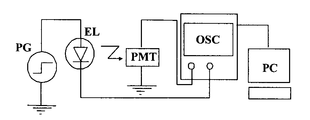
- the transient EL waveform is measured as follows (see FIG. 4).
- a pulse voltage waveform output from the voltage pulse generator (PG) is applied to the EL element.
- the applied voltage waveform is taken into an oscilloscope (OSC).
- OSC oscilloscope
- PMT photomultiplier tube
- the voltage waveform and pulse emission are synchronized and taken into a personal computer (PC).
- the TTF-derived emission intensity ratio is determined as follows by analysis of the transient EL waveform.
- the rate equation of the decay behavior of the triplet exciton is taken to model the decay behavior of the emission intensity based on the TTF phenomenon.
- the time decay of the triplet exciton density nT inside the light emitting layer can be expressed by the following rate equation using the decay rate ⁇ due to the lifetime of the triplet exciton and the decay rate ⁇ due to the collision of the triplet exciton. .
- the graph on the left of FIG. 5 is a measurement example when a predetermined DC voltage is applied to the EL element and then the voltage is removed, and shows a change over time in the emission intensity of the EL element.
- the DC voltage was removed at about 3 ⁇ 10 ⁇ 8 seconds.
- the graph represents the luminance when the voltage is removed as 1. After that, a slow decay component appears after a rapid decay up to about 2 ⁇ 10 ⁇ 7 seconds.
- the graph on the right side of FIG. 5 is a graph in which the reciprocal of the square root of the light intensity up to 10 ⁇ 5 seconds after voltage removal is plotted with the origin of voltage removal as the origin, and it can be seen that it can be approximated to a straight line well.
- the element of the present invention can have a tandem element configuration having at least two organic layer units including a light emitting layer.
- An intermediate layer also referred to as an intermediate conductive layer, a charge generation layer, or CGL
- An electron transport zone can be provided for each unit.
- At least one light emitting layer is a fluorescent light emitting layer, and a unit including the light emitting layer satisfies the above requirements.
- An example of a specific stacking order is shown below. Further, the following light emitting layer may be a laminate of a plurality of light emitting layers, or may be one organic layer unit including a charge barrier layer of a third embodiment described later.
- Anode / fluorescent layer / intermediate layer / fluorescent layer / barrier layer / cathode Anode / fluorescent layer / barrier layer / intermediate layer / fluorescent layer / cathode
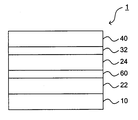
- FIG. 6 shows an example of the organic EL element according to this embodiment.
- the organic EL element 1 includes an anode 10, light emitting layers 22 and 24, and a cathode 40 in this order, and an intermediate layer 60 is provided between the light emitting layers 22 and 24.
- the barrier layer 32 is adjacent to the light emitting layer 24.
- the light emitting layer 24 is a fluorescent light emitting layer that satisfies the requirements of the present invention.
- the other light emitting layer may be fluorescent or phosphorescent.
- a barrier layer may be provided next to the light emitting layer 22 and the light emitting layer 24 may be a fluorescent light emitting layer that satisfies the requirements of the present invention.
- an electron transport band and / or a hole transport band may be interposed between the two light emitting layers 22 and 24. Further, there may be three or more light emitting layers and two or more intermediate layers. When there are three or more light emitting layers, there may or may not be an intermediate layer between all the light emitting layers.
- an anode, a plurality of light emitting layers, an electron transport zone, and a cathode are provided in this order, and a charge barrier layer is provided between any two light emitting layers of the plurality of light emitting layers,
- the light emitting layer in contact with it is a fluorescent light emitting layer and satisfies the above requirements.
- a suitable organic EL element As a configuration of a suitable organic EL element according to the present embodiment, as described in Japanese Patent No. 4134280, US Published Patent Publication US2007 / 0273270A1, International Publication WO2008 / 023623A1, an anode, a first light emitting layer, a charge
- a configuration having an electron transport band having a barrier layer for preventing diffusion of triplet excitons between the second light emitting layer and the cathode can be given. It is done.
- the charge barrier layer is provided with an energy barrier of HOMO level and LUMO level between the adjacent light emitting layers, thereby adjusting the carrier injection into the light emitting layer, and carriers of electrons and holes injected into the light emitting layer.
- This layer has the purpose of adjusting the balance.
- Anode / first light emitting layer / charge barrier layer / second light emitting layer / electron transport zone / cathode Anode / first light emitting layer / charge barrier layer / second light emitting layer / third light emitting layer / electron transport zone / cathode As in the other embodiments, it is preferable to provide a hole transport zone between the first light emitting layer and the first light emitting layer.
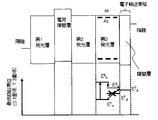
- FIG. 7 shows an example of the organic EL element according to this embodiment.
- the upper diagram of FIG. 7 shows the device configuration and the HOMO and LUMO energy levels of each layer.
- the figure below shows the relationship between the energy gap between the third light emitting layer and the barrier layer.
- the organic EL element 2 includes an anode, a first light emitting layer, a second light emitting layer, a third light emitting layer, an electron transport band, and a cathode 4 in this order, and is provided between the first light emitting layer and the second light emitting layer.
- the electron transport zone consists of a barrier layer.
- the third light emitting layer is a fluorescent light emitting layer that satisfies the requirements of the present invention.
- the first light emitting layer and the second light emitting layer may be fluorescent or phosphorescent.
- the element of the present embodiment is suitable as a white light-emitting element, and can be white by adjusting the emission color of the first light-emitting layer, the second light-emitting layer, and the third light-emitting layer.
- the light emitting layer may be only the first light emitting layer and the second light emitting layer, and the light emission color of the two light emitting layers may be adjusted to be white.
- the second light emitting layer is a fluorescent light emitting layer that satisfies the requirements of the present invention.
- the host of the first light emitting layer is a hole transporting material
- a fluorescent light emitting dopant having a main peak wavelength larger than 550 nm is added
- the host of the second light emitting layer (and the third light emitting layer) is an electron transporting material.
- the triplet energy of the hole transport material and the host is compared, it is preferable that the triplet energy is large.
- blue pixels, green pixels, and red pixels are provided side by side on the substrate.
- a blue pixel and / or a green pixel have the configuration of the first embodiment.
- FIG. 8 shows an example of the organic EL element according to this embodiment.
- a blue pixel B, a green pixel G, and a red pixel R are formed in parallel on a common substrate 100.
- the blue pixel B includes an anode 10, a hole transport zone 50, a blue light emitting layer 20B, an electron transport zone composed of a barrier layer 32, a cathode 40, and a protective layer 70 in this order from the substrate 100.
- the green pixel G includes an anode 10, a hole transport zone 50, a green light emitting layer 20G, an electron transport zone composed of a barrier layer 32, a cathode 40, and a protective layer 70 in this order from the substrate 100.
- the red pixel R includes an anode 10, a hole transport zone 50, a red light emitting layer 20R, an electron transport zone comprising a barrier layer 32, a cathode 40, and a protective layer 70 in this order from the substrate 100.
- An insulating film 200 is formed between the anodes of the adjacent pixels to maintain the insulation between the pixels.
- the barrier layer is provided in common for the blue pixel B, the red pixel R, and the green pixel G.
- the effect of the barrier layer is remarkable compared to the light emission efficiency obtained in the conventional blue fluorescent element, but the same effect of confining the triplet energy in the light emitting layer is obtained also in the green fluorescent element and the red fluorescent element. Therefore, improvement in luminous efficiency can be expected.
- the phosphorescent light-emitting layer it is possible to obtain an effect of confining triplet excitons in the light-emitting layer, preventing triplet energy diffusion and contributing to the improvement of the luminous efficiency of the phosphorescent dopant.
- the hole transport zone includes a hole transport layer, a hole transport layer, a hole injection layer, and the like.
- the hole transport zones may be common or different.
- each hole transport zone has a configuration suitable for the emission color.
- the organic layer composed of the light emitting layers 20B, G, R and the barrier layer is not limited to the configuration shown in the figure and can be changed as appropriate.
- the host and the dopant that can be used in the present invention have been described above.
- each color light emitting layer will be described below.
- the green light emitting layer is preferably composed of the following host material and dopant material.
- the host material is preferably a condensed aromatic ring derivative.
- As the condensed aromatic ring derivatives, anthracene derivatives, pyrene derivatives, and the like are more preferable in terms of light emission efficiency and light emission lifetime.
- examples of the host material include heterocyclic compounds.
- examples of the heterocyclic compound include carbazole derivatives, dibenzofuran derivatives, ladder-type furan compounds, and pyrimidine derivatives.
- the dopant material is not particularly limited as long as it has the function, but an aromatic amine derivative is preferable in terms of luminous efficiency and the like.
- an aromatic amine derivative a condensed aromatic ring derivative having an optionally substituted arylamino group is preferable. Examples of such a compound include pyrene, anthracene, and chrysene having an arylamino group.
- a styrylamine compound is also preferable as the dopant material.
- the styrylamine compound include styrylamine, styryldiamine, styryltriamine, and styryltetraamine.
- styrylamine is a compound in which at least one arylvinyl group is substituted on an optionally substituted arylamine, and the arylvinyl group may be substituted, and the substituent is an aryl group.
- a silyl group, an alkyl group, a cycloalkyl group, and an arylamino group, and these substituents may further have a substituent.
- boron complexes and fluoranthene compounds are also preferable as dopant materials.
- a metal complex is also preferable as the dopant material. Examples of metal complexes include iridium complexes and platinum complexes.
- the red light emitting layer is preferably composed of the following host material and dopant material.
- the host material is preferably a condensed aromatic ring derivative.
- a condensed aromatic ring derivative a naphthacene derivative, a pentacene derivative, or the like is more preferable in terms of light emission efficiency and light emission lifetime.
- examples of the host material include condensed polycyclic aromatic compounds.
- examples of the condensed polycyclic aromatic compound include naphthalene compounds, phenanthrene compounds, and fluoranthene compounds.
- an aromatic amine derivative is preferable.
- the aromatic amine derivative a condensed aromatic ring derivative having an optionally substituted arylamino group is preferable.
- An example of such a compound is periflanten having an arylamino group.
- metal complex is preferable as the dopant material.
- metal complexes include iridium complexes and platinum complexes.
- the element of Embodiment 4 is produced as follows, for example.
- a transparent conductive layer such as an APC (Ag—Pd—Cu) layer (reflection layer), a zinc oxide film (IZO), or a tin oxide film, which is a silver alloy layer, is formed on the substrate in this order.
- the conductive material layer is patterned by etching using a resist pattern as a mask by using a normal lithography technique to form an anode.
- an insulating film made of a photosensitive resin such as polyimide is applied and formed on the anode by spin coating. Thereafter, the blue light emitting region, the green light emitting region, and the red light emitting region are patterned by exposing, developing and curing to expose the anode.
- red pixels, green pixels, and blue pixels which correspond to the blue light emitting region, the green light emitting region, and the red light emitting region, respectively, and correspond to the anode.
- UV ozone washing is performed for 30 minutes.
- a positive hole injection layer and a positive hole transport layer a positive hole injection layer is laminated
- Each light emitting layer is formed so as to correspond to each position of the anode for the red pixel, the green pixel, and the blue pixel.
- the blue light emitting layer, the green light emitting layer, and the red light emitting layer are finely patterned using a shadow mask.
- a barrier layer is laminated over the entire surface. Subsequently, when the electron injection layer is formed, the electron injection layer is laminated over the entire surface. Then, Mg and Ag are vapor-deposited to form a cathode made of a semi-permeable MgAg alloy.
- the hole transport layer contains an aromatic amine derivative represented by any of the following formulas (1) to (5).
- Ar 1 to Ar 24 each independently represents a substituted or unsubstituted aryl group having 6 to 50 ring carbon atoms or a substituted or unsubstituted heteroaryl group having 5 to 50 ring atoms.
- L 1 to L 9 each independently represents a substituted or unsubstituted arylene group having 6 to 50 ring carbon atoms or a substituted or unsubstituted heteroarylene group having 5 to 50 ring atoms.
- the substituents that Ar 1 to Ar 24 and L 1 to L 9 may have include a linear or branched alkyl group having 1 to 15 carbon atoms, a cycloalkyl group having 3 to 15 ring carbon atoms, carbon
- An alkylarylsilyl group having an alkyl group and an aryl group having 6 to 14 ring carbon atoms, an aryl group having 6 to 50 ring carbon atoms, a heteroaryl group having 5 to 50 ring atoms, a halogen atom or a cyano group is there.
- a plurality of adjacent substituents may be bonded to each other to form a saturated or unsaturated divalent group forming a ring.
- At least one of Ar 1 to Ar 24 is a substituent represented by any one of the following formulas (6) and (7).
- X represents an oxygen atom, a sulfur atom, or N—Ra
- Ra represents a linear or branched alkyl group having 1 to 15 carbon atoms, a cycloalkyl group having 3 to 15 ring carbon atoms, It represents an aryl group having 6 to 50 ring carbon atoms or a heteroaryl group having 5 to 50 ring atoms.
- L 10 represents a single bond, a substituted or unsubstituted arylene group having 6 to 50 ring carbon atoms, or a substituted or unsubstituted heteroarylene group having 5 to 50 ring atoms.
- L 11 represents a substituted or unsubstituted arylene group having 6 to 50 ring carbon atoms or a substituted or unsubstituted heteroarylene group having 5 to 50 ring atoms.
- R 1 to R 4 are each independently a linear or branched alkyl group having 1 to 15 carbon atoms, a cycloalkyl group having 3 to 15 ring carbon atoms, a straight chain having 1 to 15 carbon atoms, A trialkylsilyl group having a branched alkyl group, a triarylsilyl group having an aryl group having 6 to 14 ring carbon atoms, a linear or branched alkyl group having 1 to 15 carbon atoms, and a ring carbon number of 6 An alkylarylsilyl group having an aryl group of ⁇ 14, an aryl group having 6 to 14 ring carbon atoms, a heteroaryl group having 5 to 50 ring atoms, a halogen atom or a
- the compound represented by the formula (1) is a compound represented by the following formula (8).
- Cz represents a substituted or unsubstituted carbazolyl group.
- L 12 represents a substituted or unsubstituted arylene group having 6 to 50 ring carbon atoms or a substituted or unsubstituted heteroarylene group having 5 to 50 ring atoms.
- Ar 25 and Ar 26 each independently represents a substituted or unsubstituted aryl group having 6 to 50 ring carbon atoms or a substituted or unsubstituted heteroaryl group having 5 to 50 ring atoms.
- the compound represented by the formula (8) is preferably a compound represented by the following formula (9).
- R 5 and R 6 are each independently a linear or branched alkyl group having 1 to 15 carbon atoms, a cycloalkyl group having 3 to 15 ring carbon atoms, or a C 1 to 15 carbon atoms.
- a plurality of R 5 and R 6 may be bonded to each other to form a ring.
- e and f each represents an integer of 0 to 4.
- L 12, Ar 25 and Ar 26 are the same meaning as L 12, Ar 25 and Ar 26 in the formula (8). )
- the compound represented by the formula (9) is preferably a compound represented by the following formula (10).
- R 7 and R 8 are each independently a linear or branched alkyl group having 1 to 15 carbon atoms, a cycloalkyl group having 3 to 15 ring carbon atoms, or a C 1 to 15 carbon atoms.
- R 5 and R 6 may be bonded to each other to form a ring.
- g and h each represents an integer of 0 to 4.
- R 5, R 6, e, f, Ar 25 and Ar 26 are the same meaning as R 5, R 6, e, f, Ar 25 and Ar 26 in the formula (9). )
- E T Triplet energy
- F-4500 commercially available apparatus F-4500 (manufactured by Hitachi).
- the ionization potential was measured using an atmospheric photoelectron spectrometer (manufactured by Riken Keiki Co., Ltd .: AC-1). Specifically, the measurement was performed by irradiating the material with light and measuring the amount of electrons generated by charge separation at that time.
- Electron mobility was evaluated using impedance spectroscopy.
- the following electronic-only device was manufactured, and the complex modulus was measured by applying a DC voltage on which an AC voltage of 100 mV was applied.
- the frequency at which the imaginary part of the modulus is maximum is f max (Hz)
- the electron mobility of TB1 and TB2 used as barrier layers at 500 (V / cm) 0.5 is 4 ⁇ 10 ⁇ 5 cm 2 / Vs, 3 ⁇ 10, respectively. It was ⁇ 5 cm 2 / Vs, and was larger than 10 ⁇ 6 cm 2 / Vs in a wide electric field strength range. It can also be seen from FIG. 9 that this value is almost the same as the electron mobility of the material ET1 used as the electron injection layer.
- the electron mobility of Alq 3 at an electric field strength of 0.25 MV / cm is 5 ⁇ 10 ⁇ 8 cm 2 / Vs
- the mobility of BCP is 1 ⁇ 10 ⁇ 7 cm 2 / Vs, which is 100 minutes from TB1 and TB2. It was a small value of 1 or less.
- the electron mobility of BPhen was 5 ⁇ 10 ⁇ 6 cm 2 / Vs, which was larger than 10 ⁇ 6 cm 2 / Vs, but was an order of magnitude smaller than TB1 and TB2.
- Example 1 HI1, HT1, BH1, BD1, TB1, and ET1 were sequentially deposited on an ITO substrate on which ITO having a thickness of 130 nm was formed, thereby obtaining an element having the following configuration.
- the parentheses indicate the film thickness (unit: nm).
- Example 1 a device was fabricated in the same manner as in Example 1 except that the thickness of the light emitting layer was 30 nm and the barrier layer TB1 was not used. ITO (130) / HI1 (50) / HT1 (45) / BH1: BD1 (30: 5 wt%) / ET1 (20) / LiF (1) / Al (80)
- Example 2 an element having the following configuration was obtained in the same manner as in Example 1 except that BH1 was used instead of TB1.
- ITO 130
- / HI1 50
- / HT1 45
- / BH1 BD1 (25: 5 wt%)
- / BH1 (5)
- ET1 20
- Example 2 An element having the following configuration was obtained in the same manner as in Example 1 except that the film thickness of BH1: BD1 was 27.5 nm and the film thickness of TB1 was 2.5 nm. ITO (130) / HI1 (50) / HT1 (45) / BH1: BD1 (27.5: 5 wt%) / TB1 (2.5) / ET1 (20) / LiF (1) / Al (80)
- Example 3 An element having the following configuration was obtained in the same manner as in Example 1, except that the film thickness of BH1: BD1 was 20 nm and the film thickness of TB1 was 10 nm.
- ITO 130) / HI1 (50) / HT1 (45) / BH1: BD1 (20; 5%) / TB1 (10) / ET1 (20) / LiF (1) / Al (80)
- Example 4 An element having the following configuration was obtained in the same manner as in Example 1 except that HT2 was used instead of HT1 and TB2 was used instead of TB1.
- ITO 130
- / HI1 50
- / HT2 45
- / BH1 BD1 (25: 5 wt%)
- / TB2 (5)
- ET1 20
- Example 1 an element having the following configuration was obtained in the same manner as in Example 1 except that BCP was used instead of TB1.
- ITO 130
- HI1 50
- HT1 45
- BH1 BD1
- BCP (5)
- ET1 20
- Example 1 an element having the following configuration was obtained in the same manner as in Example 1 except that BPhen was used instead of TB1.
- ITO 130
- / HI1 50
- / HT1 45
- / BH1 BD1 (25: 5 wt%)
- BPhen (5)
- ET1 20
- Evaluation Example 1 The following evaluations were performed on the devices obtained in Examples 1 to 4 and Comparative Examples 1 to 4. The results are shown in Table 1.
- CS-1000 spectral radiance meter
- BD1 Since the ionization potential and affinity of BH1 are 6.0 eV and 3.0 eV, respectively, and the ionization potential and affinity of BD1 are 5.5 eV and 2.7 eV, respectively, BD1 has a hole trapping property. Have.
- the triplet energy of BD1 is 2.28 eV, which is larger than the triplet energy of BH1 of 1.83 eV.
- the triplet energy of the barrier layer TB1 is 2.27 eV, which is larger than the triplet energy of BH1.
- Example 2 In Example 1 in which the barrier layer TB1 having a triplet energy larger than that of the host is used, the current efficiency is 11.7 cd / in blue with a chromaticity CIEy value of 0.164 at a current density of 1 mA / cm 2 .
- A an extremely high efficiency device having an external quantum efficiency of 9.41% and a TTF ratio of 28.7%.
- the maximum value of the TTF ratio in the current density range of 0.1 to 100 mA / cm 2 was 30.5% at a current density of 10 mA / cm 2 , showing a value exceeding 30%.
- Comparative Example 1 in which no barrier layer was used, the current efficiency showed a low value of 9.07 cd / A with the same chromaticity, and the TTF ratio was also a small value of 12.5%.
- the triplet energy of the material ET1 used for the electron injection layer is 1.82 eV, which is smaller than the triplet level 1.83 eV of the host BH1, so that triplet excitons have diffused to the electron injection layer side. Possible cause.
- Comparative Example 2 using the same BH1 as the host as the barrier layer the current efficiency was a low value of 8.72 cd / A.
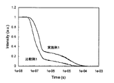
- FIG. 10 shows the transient EL waveforms of Example 1 and Comparative Example 1 when 1 mA / cm 2 is energized.
- Example 1 in which the barrier layer was provided, delayed emission derived from TTF was observed to be large, whereas in Comparative Example 1 having no barrier layer, not only the delayed emission was small but also rapid decay after voltage removal.
- the decay time of the component (light emission derived from singlet excitons immediately after recombination) is faster than that of Example 1. It can be seen that the electron-hole carrier balance is improved by providing the barrier layer.
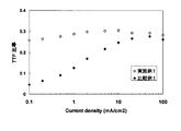
- Example 11 compares the TTF ratio in the range of 0.1 mA / cm 2 to 100 mA / cm 2 between Example 1 and Comparative Example 1.
- FIG. 1 including the barrier layer a high TTF ratio is exhibited even in a low current density region, and the efficiency is greatly increased.
- Example 1 the internal quantum efficiency at a current density of 1 mA / cm 2 was estimated to be 32.8%. Since the TTF ratio was 28.7%, the breakdown of the internal quantum efficiency was 13.4% for singlet excitons and 9.4% for TTF. On the other hand, the internal quantum efficiency of Comparative Example 1 at a current density of 1 mA / cm 2 was 27.2%. Since the TTF ratio was 12.5%, the breakdown of the internal quantum efficiency was 13.8% for singlet excitons and 3.4% for TTF. Thus, by providing the barrier layer TB1, it was possible to increase TTF-derived light emission from 3.4% to 9.4%, that is, 2.8 times.
- Example 4 when HT2 was used instead of HT1 in Example 1, and TB2 was used instead of TB1 as the barrier layer, 11.8 cd / A, which is higher efficiency than Example 1, was obtained. It was. This is probably because HT2 is closer to the ionization potential of BH1, and the amount of holes injected into the light emitting layer is increased.
- Example 5 In the same manner as in Example 1, an element having the following configuration was obtained.
- the parentheses indicate the film thickness (unit: nm).
- ITO 130) / HI1 (50) / HT1 (45) / BH2: BD2 (25: 5%) / TB2 (5) / ET2 (20) / LiF (1) / Al (80)
- Example 6 In the same manner as in Example 1, an element having the following configuration was obtained. ITO (130) / HI1 (50) / HT1 (45) / BH2: BD2 (25: 5%) / TB3 (5) / ET2 (20) / LiF (1) / Al (80)
- Example 7 In the same manner as in Example 1, an element having the following configuration was obtained. ITO (130) / HI1 (50) / HT1 (45) / BH2: BD3 (25: 5%) / TB2 (5) / ET2 (20) / LiF (1) / Al (80)
- Example 8 In the same manner as in Example 1, an element having the following configuration was obtained. ITO (130) / HI1 (50) / HT1 (45) / BH2: BD3 (25: 5%) / TB3 (5) / ET2 (20) / LiF (1) / Al (80)
- Evaluation example 2 Table 2 shows the results of evaluating the devices of Examples 5 to 8 in the same manner as in Evaluation Example 1.
- Examples 5 and 6 show that a high EQE can be obtained even when a combination of BH2 and BD2 is used.
- Af of TB3 is 3.1 eV, and it is considered that the electron injection property is improved to lower the voltage and improve the efficiency.
- Examples 7 and 8 show that even when a combination of BH2 and BD3 is used, high EQE can be obtained.
- Af of TB3 is 3.1 eV, and it is considered that the electron injection property is improved to lower the voltage and improve the efficiency.
- Example 9 In the same manner as in Example 1, an element having the following configuration was obtained.
- the parentheses indicate the film thickness (unit: nm).
- Example 10 In the same manner as in Example 1, an element having the following configuration was obtained. ITO (130) / HI2 (50) / HT5 (45) / BH3: BD6 (25; 2.5%) / TB2 (5) / ET2 (20) / LiF (1) / Al (80)
- Example 11 In the same manner as in Example 1, an element having the following configuration was obtained. ITO (130) / HI2 (50) / HT5 (45) / BH3: BD7 (25; 2.5%) / TB2 (5) / ET2 (20) / LiF (1) / Al (80)
- Evaluation Example 3 Table 3 shows the results of evaluating the devices of Examples 9 to 11 and Comparative Examples 5 and 6 in the same manner as in Evaluation Example 1.
- BD5, BD6, and BD7 were used as the BD.
- Examples 10 and 11 were very dark blue with a CIEy value of about 0.06, and therefore the TTF ratio was more than 30%, although the efficiency was low.
- Comparative Examples 5 and 6 are cases where TB2 was not used in the configurations of Examples 10 and 11, and the TTF ratios were 6.2% and 5.0%, respectively. From these results, it was shown that TB2 contributes to the improvement of TTF efficiency even when BD6 and 7 are used.
- Example 12 In the same manner as in Example 1, an element having a structure in which the following was sequentially laminated was obtained.
- the parentheses indicate the film thickness (unit: nm).
- Anode ITO 130
- Hole injection layer HI2 70
- Hole transport layer HT4 10
- HT11 10
- PBH PGD: PRD (50; 10%, 0.3%)
- Hole barrier layer PGH 10
- Electron transport layer ET2 25)
- Electron injection layer LiF 80
- Evaluation Example 4 Table 4 shows the results of evaluating the elements of Example 12 and Comparative Example 7 in the same manner as in Evaluation Example 1.
- Example 12 white light emission was exhibited by laminating a blue fluorescent portion and a red / green phosphorescent portion having the barrier layer TB2 adjacent to the blue light emitting layer through an intermediate layer.
- Comparative Example 7 does not use the barrier layer TB2.
- the EQE was 26.4% and the CIE chromaticity (0.305, 0.336).
- the EQE was 29.4% and the CIE chromaticity (0.283, 0.307).
- the organic EL element of the present invention can be used for a display panel or a lighting panel for a large-sized television where low power consumption is desired.
Abstract
Description
1.陽極と、発光層と、障壁層と、電子注入層と、陰極とをこの順に備え、
前記発光層は、ホストと、主ピーク波長が550nm以下の蛍光発光を示すドーパントとを含み、
前記ドーパントのアフィニティAdが前記ホストのアフィニティAhより小さく、
前記ドーパントの3重項エネルギーET dが前記ホストの3重項エネルギーET hより大きく、
前記障壁層の3重項エネルギーET bがET hより大きく、前記障壁層が炭化水素芳香族化合物からなる
有機エレクトロルミネッセンス素子。
2.前記陽極と発光層の間に正孔輸送帯域を備え、
前記正孔輸送帯域内に、前記発光層に隣接して正孔輸送層が設けられ、前記正孔輸送層の3重項エネルギーET hoがET hより大きい、
1に記載の有機エレクトロルミネッセンス素子。
3.前記炭化水素芳香族環化合物が、多環芳香族化合物である1又は2に記載の有機エレクトロルミネッセンス素子。
4.前記電子注入層を構成する材料が前記障壁層を構成する材料と同一である1~3のいずれかに記載の有機エレクトロルミネッセンス素子。
5.前記電子注入層を構成する材料が前記障壁層を構成する材料と同一であり、かつ前記電子注入層にドナーがドープされている1~3のいずれかに記載の有機エレクトロルミネッセンス素子。
6.前記ドーパントがピレン誘導体、アミノアントラセン誘導体、アミノクリセン誘導体、アミノピレン誘導体から選ばれる材料である1~5のいずれかに記載の有機エレクトロルミネッセンス素子。
7.前記障壁層を構成する材料の電子移動度が、電界強度0.04~0.5MV/cmの範囲において、10-6cm2/Vs以上である1~6のいずれかに記載の有機エレクトロルミネッセンス素子。
8.前記電子注入層を構成する材料の電子移動度が、電界強度0.04~0.5MV/cmの範囲において、10-6cm2/Vs以上である1~7のいずれかに記載の有機エレクトロルミネッセンス素子。
9.前記障壁層のアフィニティAb、前記電子注入層のアフィニティAeがAe-Ab<0.2eVで表わされる関係を満たす1~8のいずれかに記載の有機エレクトロルミネッセンス素子。
10.前記ホストが環式構造以外に二重結合を含まない化合物である1~9のいずれかに記載の有機エレクトロルミネッセンス素子。
11.前記ドーパントが環式構造以外に二重結合を含まない化合物である1~10のいずれかに記載の有機エレクトロルミネッセンス素子。
12.陽極と、発光層と、電子輸送帯域と、陰極とをこの順に備え、
前記発光層は、ホストと、主ピーク波長が550nm以下の蛍光発光を示すドーパントを含み、
前記ドーパントのアフィニティレベルAdが前記ホストのアフィニティレベルAhより小さく、
前記ドーパントの3重項エネルギーET dが前記ホストの3重項エネルギーET hより大きく、
前記電子輸送帯域内に、前記発光層に隣接して障壁層が設けられ、前記障壁層を形成する材料の3重項エネルギーET bがET hより大きく、電流効率(単位:cd/A)が最大となる印加電圧において、前記発光層に生成する3重項励起子同士が衝突して生成する1重項励起子由来の発光強度が、全発光強度に対して30%以上である
有機エレクトロルミネッセンス素子。
13.前記陽極と前記陰極の間に2つ以上の発光層を有し、2つの発光層の間に中間層を備える1~12のいずれかに記載の有機エレクトロルミネッセンス素子。
14.前記陽極と前記陰極の間に複数の発光層を含み、第一の発光層と第二の発光層の間に電荷障壁層を備える1~12のいずれかに記載の有機エレクトロルミネッセンス素子。
本発明はTTF現象を利用したものである。まず、以下にTTF現象を説明する。
陽極、陰極から注入された正孔、電子は発光層内で再結合し励起子を生成する。そのスピン状態は、従来から知られているように、1重項励起子が25%、3重項励起子が75%の比率である。従来知られている蛍光素子においては、25%の1重項励起子が基底状態に緩和するときに光を発するが、残りの75%の3重項励起子については光を発することなく熱的失活過程を経て基底状態に戻る。従って、従来の蛍光素子の内部量子効率の理論限界値は25%といわれていた。
3A*+3A*→(4/9)1A+(1/9)1A*+(13/9)3A*
即ち、53A*→41A+1A*となり、当初生成した75%の3重項励起子のうち、1/5即ち20%が1重項励起子に変化することが予測されている。従って、光として寄与する1重項励起子は当初生成する25%分に75%×(1/5)=15%を加えた40%ということになる。このとき、全発光強度中に占めるTTF由来の発光比率(TTF比率)は、15/40、すなわち37.5%となる。また、当初生成した75%の3重項励起子のお互いが衝突して1重項励起子が生成した(2つの3重項励起子から1つの1重項励起子が生成した)とすると、当初生成する1重項励起子25%分に75%×(1/2)=37.5%を加えた62.5%という非常に高い内部量子効率が得られることとなる。このとき、TTF比率は37.5/62.5=60%となる。
障壁層を形成する材料としては、好ましくは炭化水素芳香族環化合物を選択する。より好ましくは、多環芳香族化合物を選択する。これらの材料は耐正孔性があるので劣化し難く寿命が長くなる。
本発明では、Ah>Adという関係を満たすドーパントを選択する。本発明で用いるドーパントは、主ピーク波長が550nm以下の蛍光発光を示すドーパント(以下、主ピーク波長550nm以下の蛍光発光性ドーパントともいう)であり、エネルギーギャップは比較的大きくなる。従って、Ah>Adという関係を満たすとき、同時にIh>Idという関係を満たすため、ドーパントは正孔トラップとして機能しやすくなる。
ホストとドーパントの組合せの好ましい例としては、ホストとしてのアントラセン誘導体と、ドーパントとして、ピレン誘導体、アミノアントラセン誘導体、アミノクリセン誘導体、アミノピレン誘導体から選ばれる少なくとも1種以上のドーパントの組合せである。
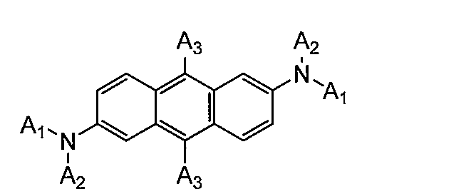
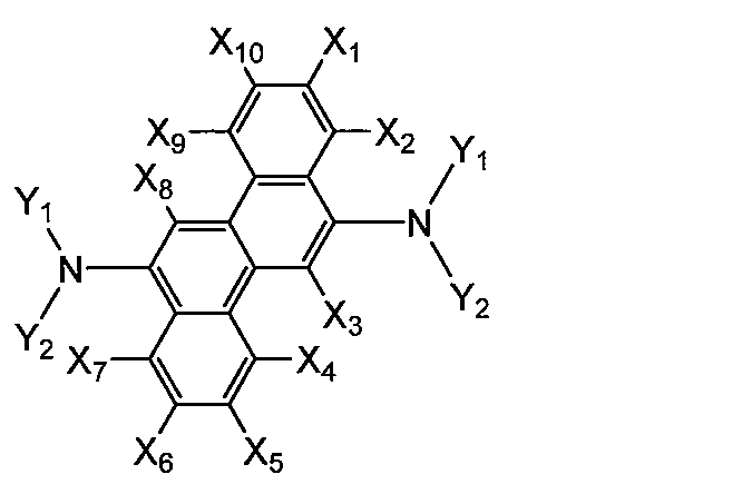
好ましくは、X1-10はHである。好ましくは、Y1,Y2は置換(好ましくはC1-6アルキルで置換)又は無置換のC6-30芳香族環(好ましくはC6-10又はフェニル)である。
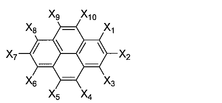

R1~R8は、それぞれ独立に、水素原子、置換もしくは無置換の環形成炭素数6~50のアリール基、置換もしくは無置換の環形成原子数5~50の複素環基、置換もしくは無置換の炭素数1~50のアルキル基、置換もしくは無置換の環形成炭素数3~50のシクロアルキル基、置換もしくは無置換の炭素数1~50のアルコキシ基、置換もしくは無置換の炭素数7~50のアラルキル基、置換もしくは無置換の環形成炭素数6~50のアリールオキシ基、置換もしくは無置換の環形成炭素数6~50のアリールチオ基、置換もしくは無置換の炭素数2~50のアルコキシカルボニル基、置換もしくは無置換のシリル基、カルボキシル基、ハロゲン原子、シアノ基、ニトロ基及びヒドロキシル基から選ばれる基である。
当該アントラセン誘導体は、式(10)におけるAr11及びAr12が、それぞれ独立に、置換もしくは無置換の環形成炭素数10~50の縮合アリール基となっている。当該アントラセン誘導体としては、Ar11及びAr12が同一の置換もしくは無置換の縮合アリール基である場合、及び異なる置換もしくは無置換の縮合アリール基である場合に分けることができる。
具体的には、下記式(2-1)~(2-3)で表されるアントラセン誘導体、及び式(10)におけるAr11及びAr12が異なる置換もしくは無置換の縮合アリール基であるアントラセン誘導体が挙げられる。
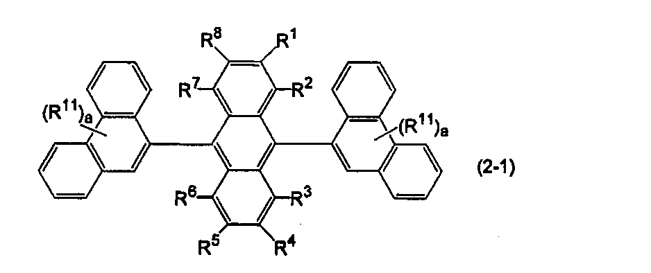
R11は水素原子、置換もしくは無置換の環形成炭素数6~50のアリール基、置換もしくは無置換の環形成原子数5~50の複素環基、置換もしくは無置換の炭素数1~50のアルキル基、置換もしくは無置換の環形成炭素数3~50のシクロアルキル基、置換もしくは無置換の炭素数1~50のアルコキシ基、置換もしくは無置換の炭素数7~50のアラルキル基、置換もしくは無置換の環形成炭素数6~50のアリールオキシ基、置換もしくは無置換の環形成炭素数6~50のアリールチオ基、置換もしくは無置換の炭素数2~50のアルコキシカルボニル基、置換もしくは無置換のシリル基、カルボキシル基、ハロゲン原子、シアノ基、ニトロ基及びヒドロキシル基から選ばれる基であり、
aは0~9の整数である。aが2以上の整数の場合、複数あるR11は、2つの置換もしくは無置換のフェナントレニル基が同一であることを条件に、それぞれが同一でも異なっていてもよい。)

bは1~7の整数である。bが2以上の整数の場合、複数あるR11は、2つの置換もしくは無置換の2-ナフチル基が同一であることを条件に、それぞれが同一でも異なっていてもよい。)
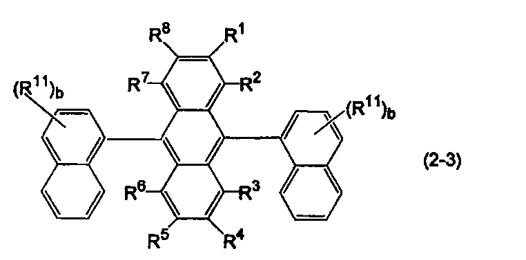
具体的には、Ar11が1-ナフチル基、及びAr12が2-ナフチル基である場合、Ar11が1-ナフチル基及びAr12が9-フェナントリル基である場合、並びにAr11が2-ナフチル基及びAr12が9-フェナントリル基である場合である。
当該アントラセン誘導体は、式(10)におけるAr11及びAr12の一方が置換もしくは無置換のフェニル基であり、他方が置換もしくは無置換の環形成炭素数10~50の縮合アリール基となっている。当該アントラセン誘導体としては、具体的には、下記式(2-4)及び(2-5)で表されるアントラセン誘導体が挙げられる。
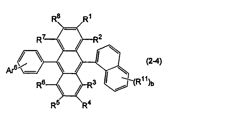
Ar6は置換もしくは無置換の環形成炭素数6~50のアリール基、置換もしくは無置換の炭素数1~50のアルキル基、置換もしくは無置換の環形成炭素数3~50のシクロアルキル基、置換もしくは無置換の炭素数7~50のアラルキル基、置換もしくは無置換の環形成原子数5~50の複素環基、9,9-ジメチルフルオレン-1-イル基、9,9-ジメチルフルオレン-2-イル基、9,9-ジメチルフルオレン-3-イル基、9,9-ジメチルフルオレン-4-イル基、ジベンゾフラン-1-イル基、ジベンゾフラン-2-イル基、ジベンゾフラン-3-イル基、又はジベンゾフラン-4-イル基である。また、Ar6はそれが結合しているベンゼン環と共に、置換もしくは無置換のフルオレニル基や置換もしくは無置換のジベンゾフラニル基等の環を形成していてもよい。bが2以上の整数の場合、複数あるR11は、それぞれが同一でも異なっていてもよい。)
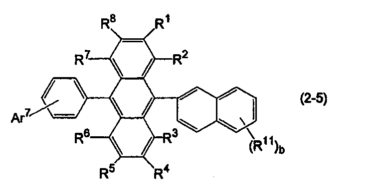
Ar7は、置換もしくは無置換の環形成炭素数6~50のアリール基、置換もしくは無置換の環形成原子数5~50の複素環基、置換もしくは無置換の炭素数1~50のアルキル基、置換もしくは無置換の環形成炭素数3~50のシクロアルキル基、置換もしくは無置換の炭素数7~50のアラルキル基、ジベンゾフラン-1-イル基、ジベンゾフラン-2-イル基、ジベンゾフラン-3-イル基、又はジベンゾフラン-4-イル基である。また、Ar7はそれが結合しているベンゼン環と共に、置換もしくは無置換のフルオレニル基や置換もしくは無置換のジベンゾフラニル基等の環を形成していてもよい。bが2以上の整数の場合、複数あるR11は、それぞれが同一でも異なっていてもよい。)
当該アントラセン誘導体は、下記式(2-6)で表され、具体的には、下記式(2-6-1)、(2-6-2)及び(2-6-3)のいずれかで表される誘導体であることが好ましい。
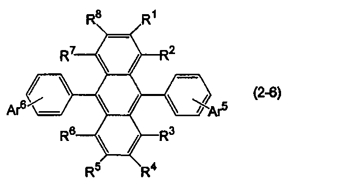
Ar5は置換もしくは無置換の環形成炭素数6~50のアリール基、置換もしくは無置換の炭素数1~50のアルキル基、置換もしくは無置換の環形成炭素数3~50のシクロアルキル基、置換もしくは無置換の炭素数7~50のアラルキル基、又は置換もしくは無置換の環形成原子数5~50の複素環基であり、Ar5とAr6はそれぞれ独立に選択される。)
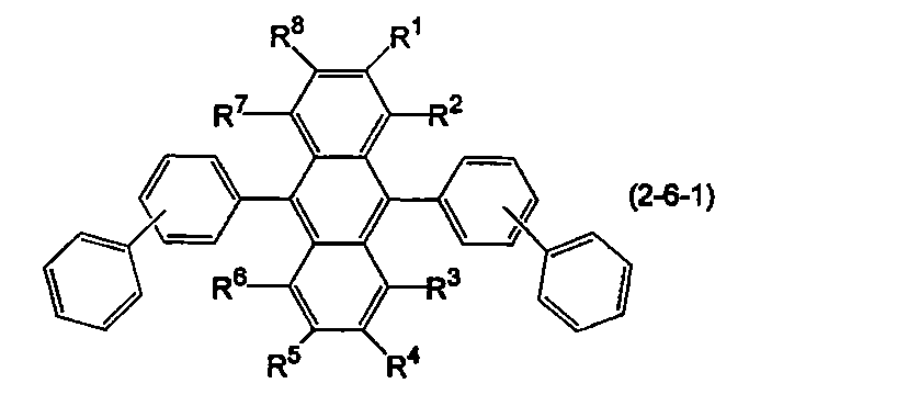
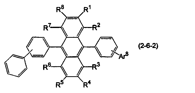
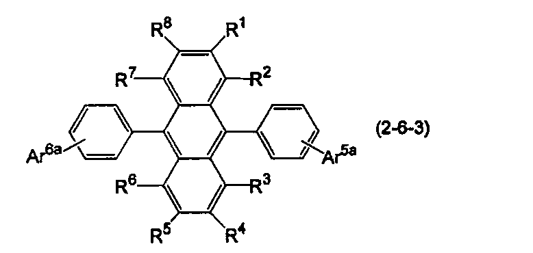
Ar5a及びAr6aはそれぞれ独立に、置換もしくは無置換の環形成炭素数10~20の縮合アリール基である。)
この場合には、Ae(電子注入層のアフィニティ)-Ab(障壁層のアフィニティ)≦0.2eVであることが好ましい。これを満たさない場合、電子注入層から障壁層への電子注入が損なわれ、電子輸送帯域に電子が蓄積し、高電圧化を引き起こすとともに、蓄積電子が3重項励起子と衝突してエネルギーがクエンチされる。
ここで、本発明における障壁層を構成する材料の電子移動度は、電界強度0.04~0.5MV/cmの範囲において、10-6cm2/Vs以上であることが望ましい。
さらに、本発明における電子注入層は、電界強度0.04~0.5MV/cmの範囲において、10-6cm2/Vs以上であることが望ましい。発光層への電子注入を促進し、発光層内の励起子密度を高め、TTF現象を効率よく起こすためである。
ドナー性金属化合物とは、上記のドナー性金属を含む化合物であり、好ましくはアルカリ金属、アルカリ土類金属又は希土類金属を含む化合物であり、より好ましくはこれらの金属のハロゲン化物、酸化物、炭酸塩、ホウ酸塩である。例えば、MOx(Mはドナー性金属、xは0.5~1.5)、MFx(xは1~3)、M(CO3)x(xは0.5~1.5)で表される化合物である。
上記のドナーは一種単独で使用してもよいし、二種以上を組み合わせて使用してもよい。
Ra-Ar101-Rb ・・・(A)
Ra-Ar101-Ar102-Rb ・・・(B)
Ra-Ar101-Ar102-Ar103-Rb ・・・(C)
多環芳香族骨格部の置換基としては、例えば、ハロゲン原子、ヒドロキシル基、置換若しくは無置換のアミノ基、ニトロ基、シアノ基、置換若しくは無置換のアルキル基、置換若しくは無置換のアルケニル基、置換若しくは無置換のシクロアルキル基、置換若しくは無置換のアルコキシ基、置換若しくは無置換の芳香族炭化水素基、置換若しくは無置換の芳香族複素環基、置換若しくは無置換のアラルキル基、置換若しくは無置換のアリールオキシ基、置換若しくは無置換のアルコキシカルボニル基、又は、カルボキシル基が挙げられる。芳香族炭化水素基の好ましい例としては、ナフタレン、フェナントレン、フルオレン、クリセン、フルオランテン及びトリフェニレンを挙げることができる。
多環芳香族骨格部が複数の置換基を有する場合、それらが環を形成していてもよい。
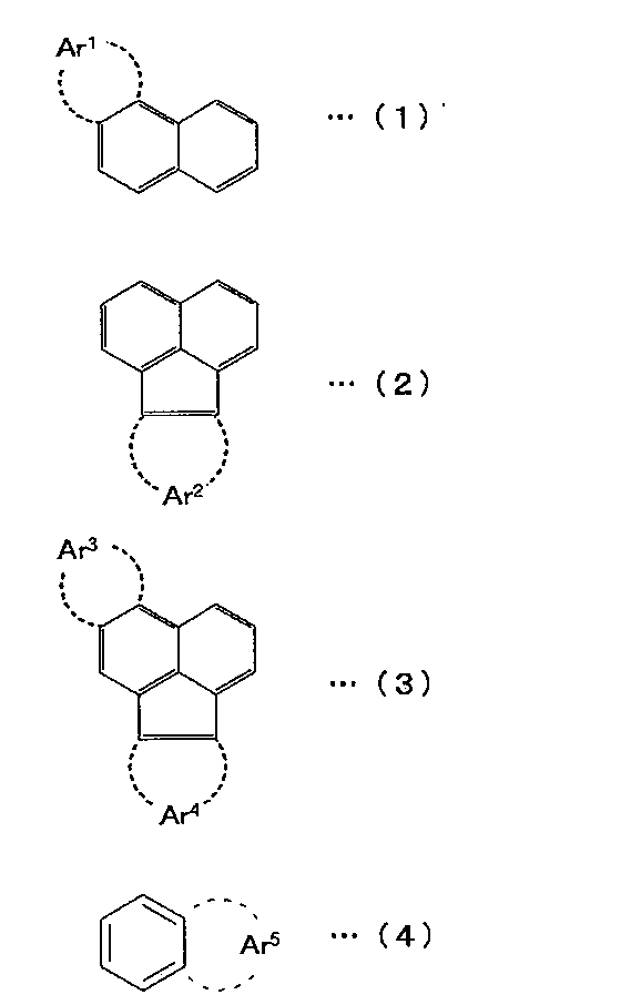
式(1)で表される化合物としては、例えば、置換若しくは無置換のフェナントレン、クリセンの単体又は誘導体等が挙げられる。
式(2)で表される化合物としては、例えば、置換若しくは無置換のアセナフチレン、アセナフテン、フルオランテンの単体又は誘導体等が挙げられる。
式(3)で表される化合物としては、例えば、置換若しくは無置換のベンゾフルオランテンの単体又は誘導体等が挙げられる。
式(4)で表される化合物としては、例えば、置換若しくは無置換のナフタレンの単体又は誘導体等が挙げられる。
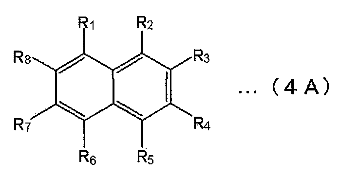
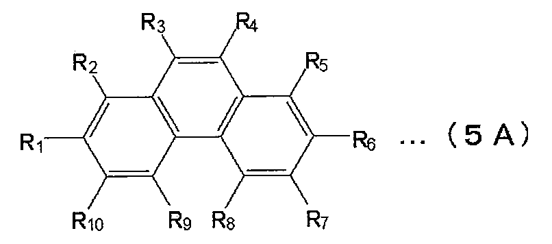
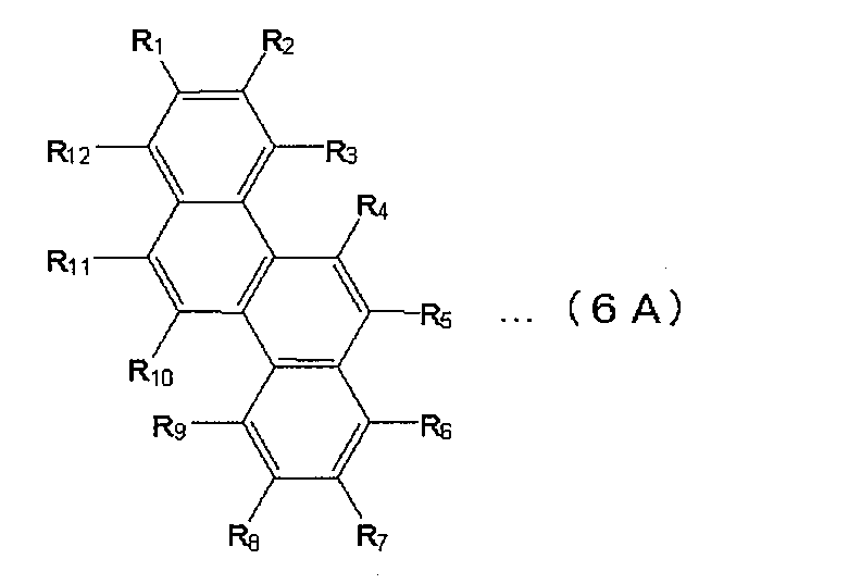
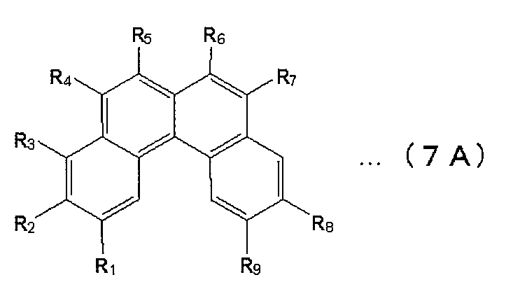

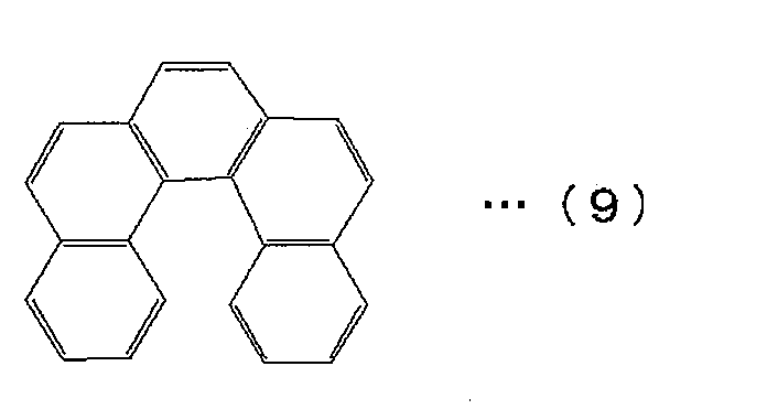
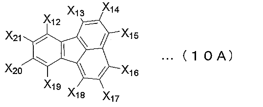
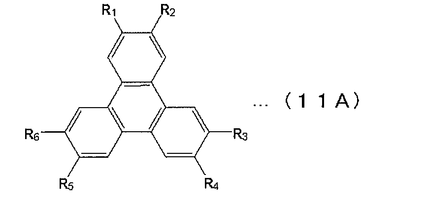

式(12)中、Ra、Rbは、フルオレン環、フェナントレン環、トリフェニレン環、ベンゾフェナントレン環、ジベンゾフェナントレン環、ベンゾトリフェニレン環、フルオランテン環、ベンゾクリセン環、ベンゾ[b]フルオランテン環及びピセン環から選択される基であることが好ましい。
電子移動度=(障壁層材料の膜厚)2/(応答時間・電圧)
ホスト、ドーパント及び障壁層材料の三重項エネルギーが所定の関係を満たすことにより、全発光に対するTTF由来の発光強度比を30%以上とすることができ、従来知られていた蛍光素子では達成できなかった高効率化を可能とすることができる。


本発明の素子は、発光層を含む有機層ユニットを少なくとも2つ有するタンデム素子構成とすることができる。2つの発光層の間には中間層(中間導電層、電化発生層、CGLとも呼ぶ)が介在する。ユニット毎に電子輸送帯域を設けることができる。少なくとも1つの発光層が蛍光発光層でありその発光層を含むユニットが上記の要件を満たす。具体的な積層順の例を以下に示す。また、下記発光層は、複数の発光層の積層体であってもよく、後述する第3の実施形態の電荷障壁層を含む一の有機層ユニットであっても良い。
陽極/蛍光発光層/中間層/蛍光発光層/障壁層/陰極
陽極/蛍光発光層/障壁層/中間層/蛍光発光層/陰極
陽極/蛍光発光層/障壁層/中間層/蛍光発光層/障壁層/陰極
陽極/りん光発光層/中間層/蛍光発光層/障壁層/陰極
陽極/蛍光発光層/障壁層/中間層/りん光発光層/陰極
本実施形態では、陽極と、複数の発光層と、電子輸送帯域と、陰極をこの順に備え、複数の発光層のいずれか二つの発光層の間に電荷障壁層を有し、電荷障壁層に接する発光層が蛍光発光層であり、上記の要件を満たす。
陽極/第1発光層/電荷障壁層/第2発光層/電子輸送帯域/陰極
陽極/第1発光層/電荷障壁層/第2発光層/第3発光層/電子輸送帯域/陰極
尚、陽極と第1発光層の間には、他の実施形態と同様に正孔輸送帯域を設けることが好ましい。
この有機EL素子2は、陽極と、第1発光層、第2発光層、第3発光層と、電子輸送帯域と、陰極4をこの順に備え、第1発光層と第2発光層の間には、電荷障壁層がある。電子輸送帯域は障壁層からなる。第3発光層が本発明の要件を満たす蛍光発光層である。第1発光層、第2発光層は蛍光型でも燐光型でもよい。
本実施形態では、青色画素、緑色画素、赤色画素を、基板上に並べて設ける。これら3色の画素のうち、青色画素及び/又は緑色画素が第1の実施形態の構成を有する。
この図に示す上面発光型有機EL素子3は、共通基板100上に、青色画素B、緑色画素G及び赤色画素Rが並列に形成されている。
緑色画素Gは、陽極10、正孔輸送帯域50、緑色発光層20G、障壁層32からなる電子輸送帯域、陰極40、保護層70を基板100からこの順に備えている。
赤色画素Rは、陽極10、正孔輸送帯域50、赤色発光層20R、障壁層32からなる電子輸送帯域、陰極40、保護層70を基板100からこの順に備えている。
それぞれの隣接する画素の陽極間に絶縁膜200が形成され、画素間の絶縁を保持している。
有機EL素子3では、障壁層が青色画素B、赤色画素R、緑色画素Gに共通に設けられている。
一方、燐光発光層においては、三重項励起子を発光層内に閉じ込める効果を得ることが可能であり、三重項エネルギーの拡散を防ぎ、燐光発光性ドーパントの発光効率の向上に寄与する。
発光層20B,G,Rと障壁層から構成される有機層は、図に示す構成に限定されず適宜変更できる。
緑色発光層は、以下のホスト材料及びドーパント材料から構成されるのが好ましい。ホスト材料は、縮合芳香族環誘導体が好ましい。縮合芳香族環誘導体としては、アントラセン誘導体、ピレン誘導体等が、発光効率や発光寿命の点でさらに好ましい。
基板上に、銀合金層であるAPC(Ag-Pd-Cu)層(反射層)、酸化亜鉛膜(IZO)や酸化錫膜等の透明導電層をこの順に成膜する。続いて通常のリソグラフィ技術を用いて、レジストパターンをマスクに用いたエッチングにより、この導電材料層をパターニングし、陽極を形成する。次に、陽極の上にスピンコート法により、ポリイミド等の感光性樹脂からなる絶縁膜を塗布形成する。その後、露光、現像、硬化することで、陽極を露出させることにより青発光領域、緑発光領域、赤発光領域をパターンニングする。
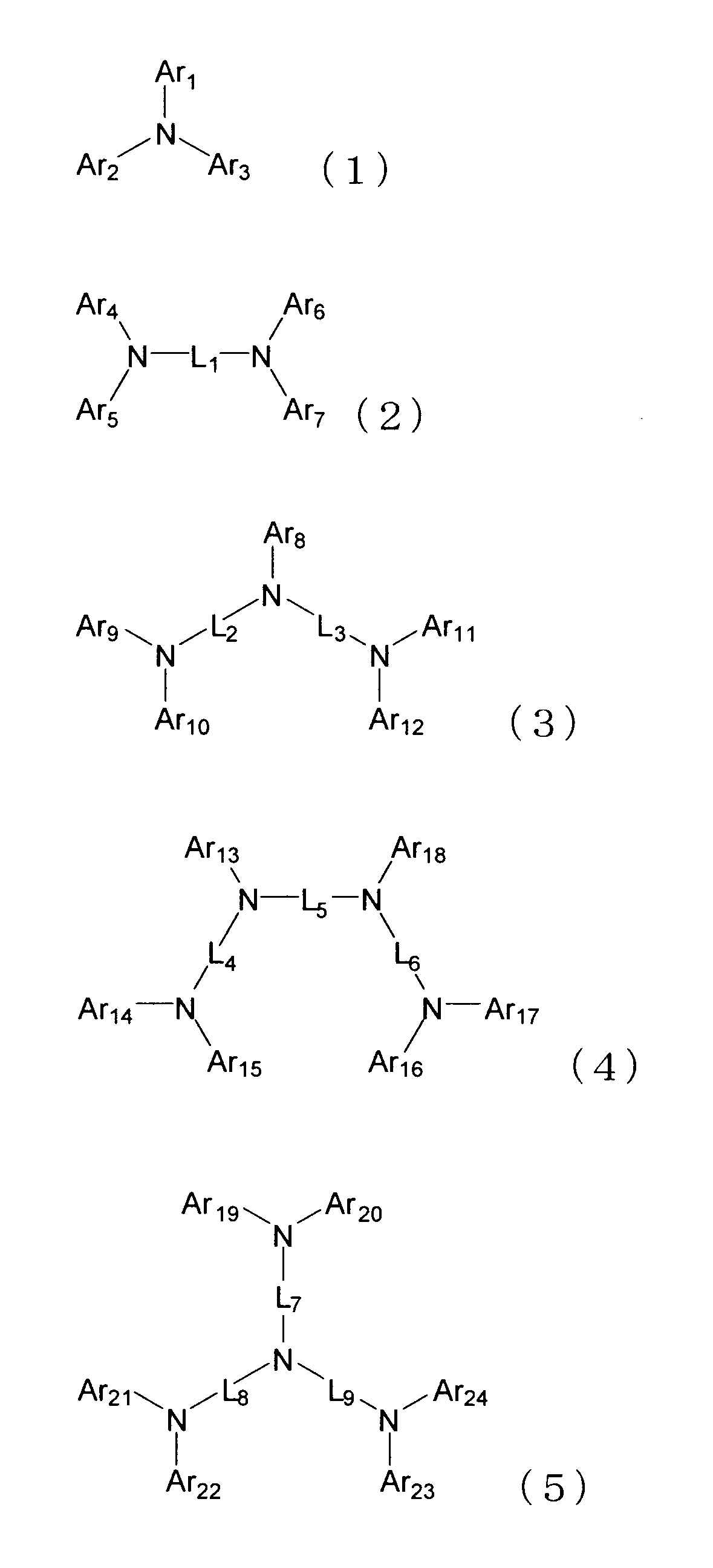
L1~L9は、各々独立して、置換もしくは無置換の環形成炭素数6~50のアリーレン基、又は置換もしくは無置換の環形成原子数5~50のヘテロアリーレン基を表わす。
Ar1~Ar24、L1~L9が有してもよい置換基は、炭素数1~15の直鎖状もしくは分岐状のアルキル基、環形成炭素数3~15のシクロアルキル基、炭素数1~15の直鎖状もしくは分岐状のアルキル基を有するトリアルキルシリル基、環形成炭素数6~14のアリール基を有するトリアリールシリル基、炭素数1~15の直鎖状もしくは分岐状のアルキル基及び環形成炭素数6~14のアリール基を有するアルキルアリールシリル基、環形成炭素数6~50のアリール基、環形成原子数5~50のヘテロアリール基、ハロゲン原子又はシアノ基である。隣接した複数の置換基は、互いに結合して、環を形成する飽和もしくは不飽和の2価の基を形成してもよい。)
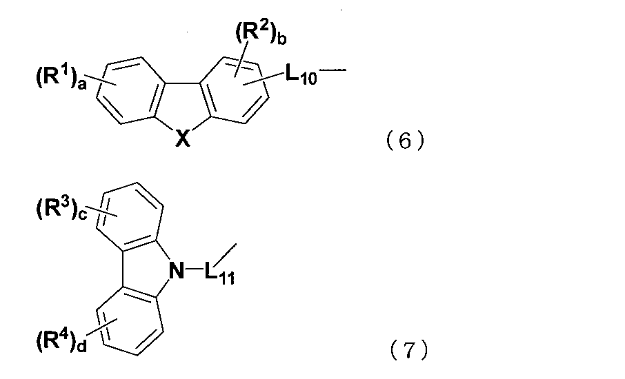
L10は、単結合、置換もしくは無置換の環形成炭素数6~50のアリーレン基、又は置換もしくは無置換の環形成原子数5~50のヘテロアリーレン基を表わす。
L11は、置換もしくは無置換の環形成炭素数6~50のアリーレン基、又は置換もしくは無置換の環形成原子数5~50のヘテロアリーレン基を表わす。
R1~R4は、各々独立して、炭素数1~15の直鎖状もしくは分岐状のアルキル基、環形成炭素数3~15のシクロアルキル基、炭素数1~15の直鎖状もしくは分岐状のアルキル基を有するトリアルキルシリル基、環形成炭素数6~14のアリール基を有するトリアリールシリル基、炭素数1~15の直鎖状もしくは分岐状のアルキル基及び環形成炭素数6~14のアリール基を有するアルキルアリールシリル基、環形成炭素数6~14のアリール基、環形成原子数5~50のヘテロアリール基、ハロゲン原子又はシアノ基を表す。また、隣接した複数のR1~R4は互いに結合して環を形成してもよい。
a、c、dは0~4の整数を表わす。
bは0~3の整数を表わす。)
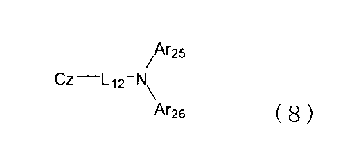
L12は置換もしくは無置換の環形成炭素数6~50のアリーレン基、又は置換もしくは無置換の環形成原子数5~50のヘテロアリーレン基を表わす。
Ar25及びAr26は、各々独立して、置換もしくは無置換の環形成炭素数6~50のアリール基、又は置換もしくは無置換の環形成原子数5~50のヘテロアリール基を表わす。)

e、fは0~4の整数を表わす。
L12、Ar25及びAr26は、式(8)におけるL12、Ar25及びAr26と同義である。)
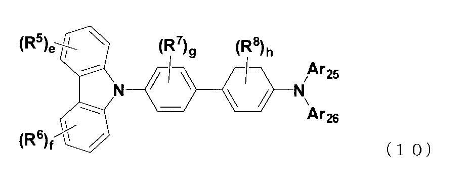
g、hは0~4の整数を表わす。
R5、R6、e、f、Ar25及びAr26は、式(9)におけるR5、R6、e、f、Ar25及びAr26と同義である。)
実施例及び比較例で使用した材料と物性値は以下の通りである。
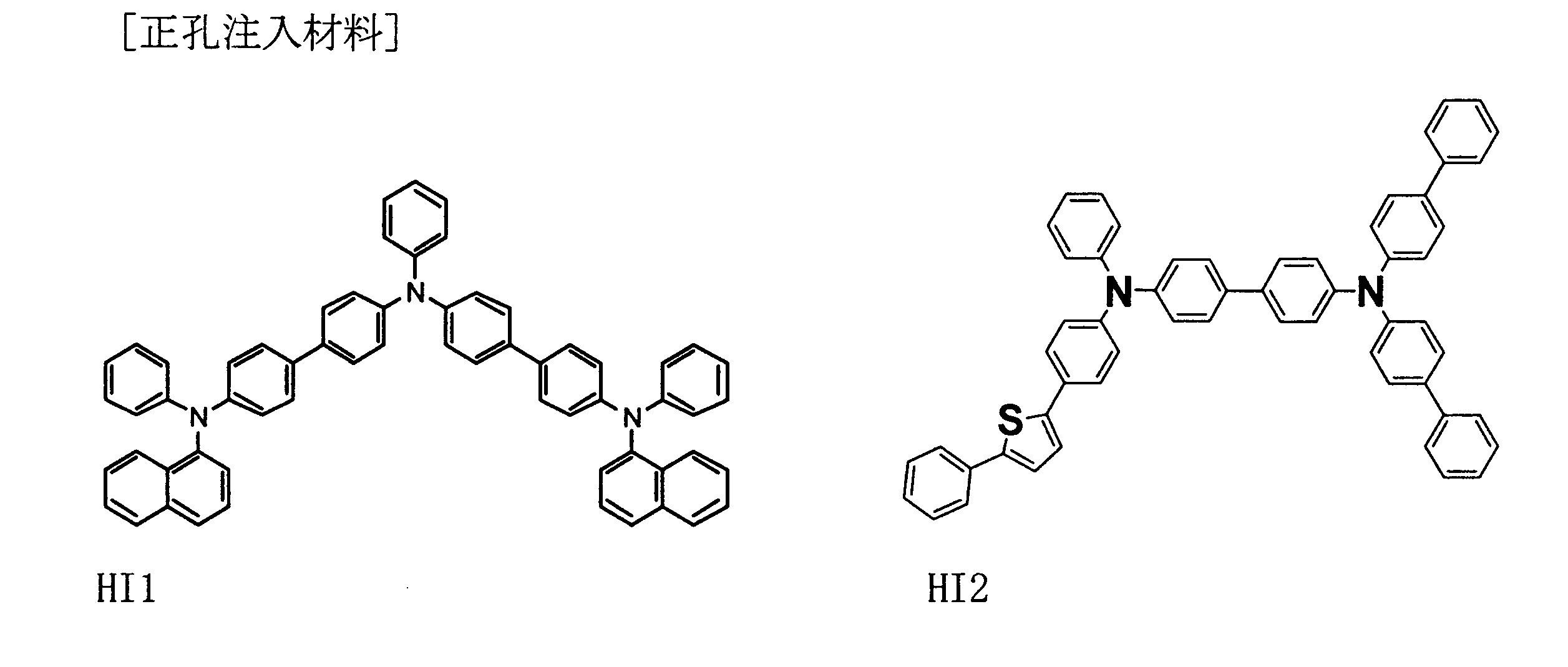


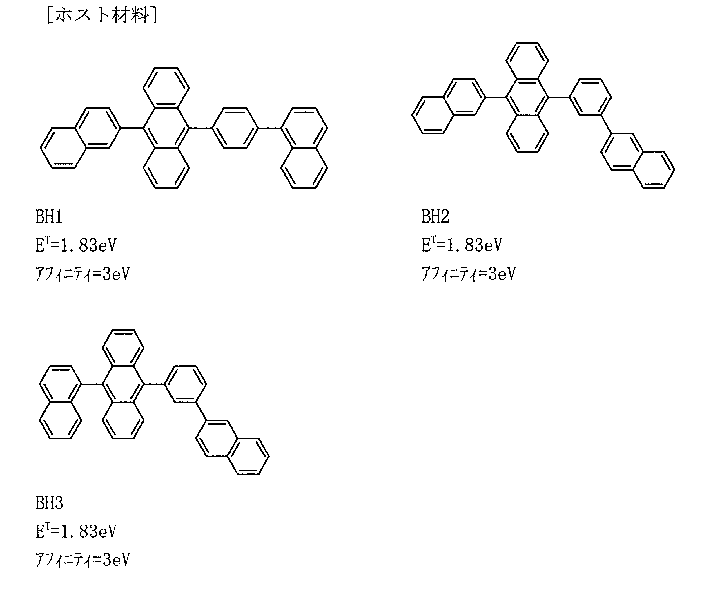


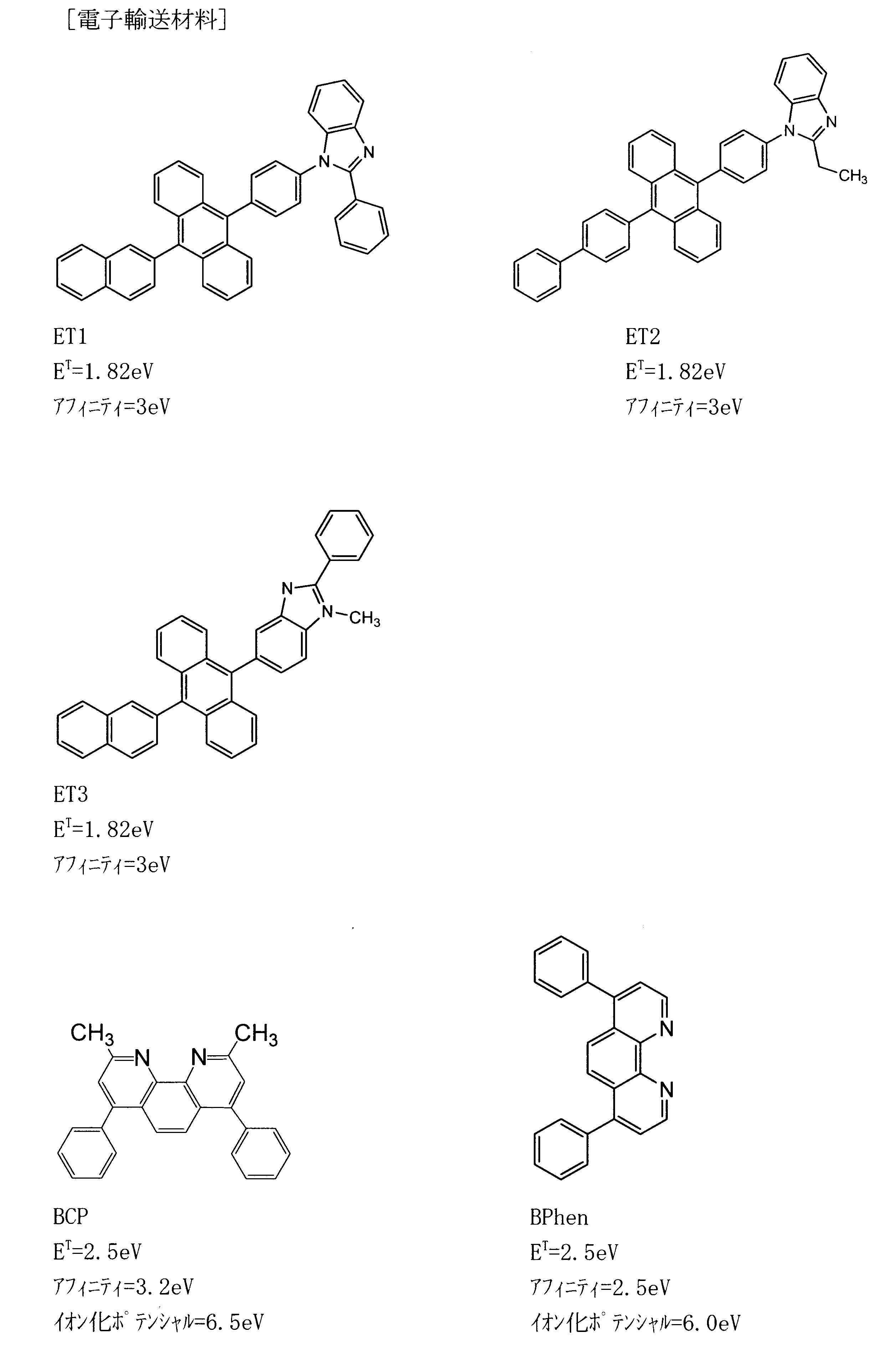
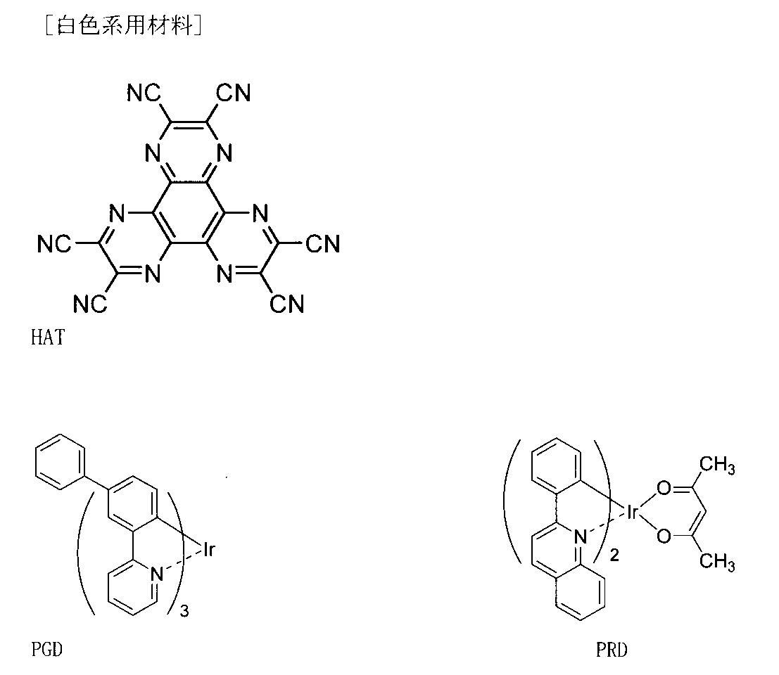
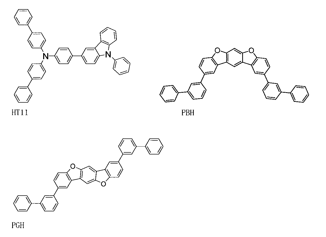
(1)3重項エネルギー(ET)
市販の装置F-4500(日立社製)を用いて測定した。ETの換算式は以下の通りである。
換算式 ET(eV)=1239.85/λedge
「λedge」とは、縦軸にりん光強度、横軸に波長をとって、りん光スペクトルを表したときに、りん光スペクトルの短波長側の立ち上がりに対して接線を引き、その接線と横軸の交点の波長値を意味する。単位:nm。
大気下光電子分光装置(理研計器(株)社製:AC-1)を用いて測定した。具体的には、材料に光を照射し、その際に電荷分離によって生じる電子量を測定することにより測定した。
イオン化ポテンシャルとエネルギーギャップの測定値から算出した。エネルギーギャップはベンゼン中の吸収スペクトルの吸収端から測定した。具体的には、市販の可視・紫外分光光度計を用いて、吸収スペクトルを測定し、そのスペクトルが立ち上がり始める波長から算出した。
インピーダンス分光法を用いて電子移動度評価を行った。以下のような電子オンリーデバイスを作製し、100mVの交流電圧を乗せたDC電圧を印加し複素モジュラスを測定した。モジュラスの虚部が最大となる周波数をfmax(Hz)としたとき、応答時間T(秒)をT=1/2/π/fmaxとして算出し、この値を用いて電子移動度の電界強度依存性を決定した。
Al/TB2(95)/ET1(5)/LiF(1)/Al
Al/ET1(100)/LiF(1)/Al
Al/Alq3(100)/LiF(1)/Al
(括弧内の数値は膜厚。単位:nm)
特開2006-278035に記載の方法にもとづき発光層内での発光分布と光取出し効率を決定した。その後、分光放射輝度計で測定したELスペクトルを、決定した光取り出し効率で割り、内部ELスペクトルを求め、そのスペクトルから求められる内部発生光子数と電子数の比を内部量子効率とした。
膜厚130nmのITOが成膜されたITO基板上に、HI1、HT1、BH1、BD1、TB1、ET1を順次蒸着し、下記の構成からなる素子を得た。括弧内は膜厚(単位:nm)を示す。
ITO(130)/HI1(50)/HT1(45)/BH1:BD1(25:5wt%)/TB1(5)/ET1(20)/LiF(1)/Al(80)
実施例1において、発光層の膜厚を30nmとし、障壁層TB1を用いなかったこと以外は実施例1と同様に素子を作製した。
ITO(130)/HI1(50)/HT1(45)/BH1:BD1(30:5wt%)/ET1(20)/LiF(1)/Al(80)
実施例1において、TB1の代わりにBH1を用いた他は実施例1と同様にして下記の構成からなる素子を得た。
ITO(130)/HI1(50)/HT1(45)/BH1:BD1(25:5wt%)/BH1(5)/ET1(20)/LiF(1)/Al(80)
実施例1において、BH1:BD1の膜厚を27.5nmとし、TB1の膜厚を2.5nmとした他は実施例1と同様にして下記の構成からなる素子を得た。
ITO(130)/HI1(50)/HT1(45)/BH1:BD1(27.5:5wt%)/TB1(2.5)/ET1(20)/LiF(1)/Al(80)
実施例1において、BH1:BD1の膜厚を20nmとし、TB1の膜厚を10nmとした他は実施例1と同様にして下記の構成からなる素子を得た。
ITO(130)/HI1(50)/HT1(45)/BH1:BD1(20;5%)/TB1(10)/ET1(20)/LiF(1)/Al(80)
実施例1において、HT1の代わりにHT2を用い、TB1の代わりにTB2を用いた他は実施例1と同様にして下記の構成からなる素子を得た。
ITO(130)/HI1(50)/HT2(45)/BH1:BD1(25:5wt%)/TB2(5)/ET1(20)/LiF(1)/Al(80)
実施例1において、TB1の代わりにBCPを用いた他は実施例1と同様にして下記の構成からなる素子を得た。
ITO(130)/HI1(50)/HT1(45)/BH1:BD1(25:5wt%)/BCP(5)/ET1(20)/LiF(1)/Al(80)
実施例1において、TB1の代わりにBPhenを用いた他は実施例1と同様にして下記の構成からなる素子を得た。
ITO(130)/HI1(50)/HT1(45)/BH1:BD1(25:5wt%)/BPhen(5)/ET1(20)/LiF(1)/Al(80)
実施例1~4、比較例1~4で得られた素子について以下の評価を行った。結果を表1に示す。
(1)初期性能(電圧、色度、電流効率、外部量子効率、主ピーク波長)
電流値が1mA/cm2となるように素子に電圧を印加し、そのときの電圧値を測定した。またそのときのEL発光スペクトルを分光放射輝度計(CS-1000:コミカミノルタ社製)を用いて計測した。得られた分光放射輝度スペクトルから、色度、電流効率(cd/A)、外部量子効率(%)、主ピーク波長(nm)を算出した。
パルスジェネレータ(アジレント社製8114A)から出力した電圧パルス波形(パルス幅:500マイクロ秒、周波数:20Hz、電圧:0.1~100mA/cm2相当の電圧を印加し、EL発光を光電子増倍管(浜松ホトニクス社製R928)に入力し、パルス電圧波形とEL発光とを同期させてオシロスコープ(テクトロニクス社製2440)に取り込んで過渡EL波形を得た。これを解析してTTF由来の発光比率(TTF比率)を決定した。
なお、TTF現象による内部量子効率の向上は62.5%が理論的限界と考えられ、この場合のTTF由来の発光比率は60%になる。
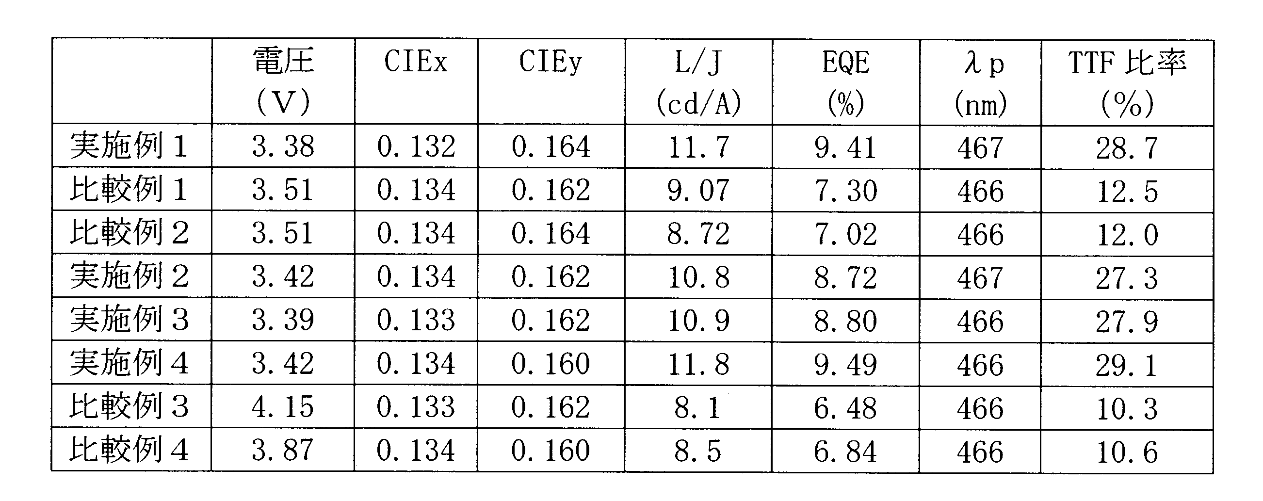
一方、比較例1の電流密度1mA/cm2での内部量子効率は27.2%であった。TTF比率は12.5%であるから、内部量子効率の内訳は1重項励起子の発光が23.8%、TTF由来の発光が3.4%であった。このように、障壁層TB1を設けることにより、TTF由来の発光を3.4%から9.4%、すなわち2.8倍に高めることができた。
実施例1と同様にして、下記の構成からなる素子を得た。括弧内は膜厚(単位:nm)を示す。
ITO(130)/HI1(50)/HT1(45)/BH2:BD2(25:5%)/TB2(5)/ET2(20)/LiF(1)/Al(80)
実施例1と同様にして、下記の構成からなる素子を得た。
ITO(130)/HI1(50)/HT1(45)/BH2:BD2(25:5%)/TB3(5)/ET2(20)/LiF(1)/Al(80)
実施例1と同様にして、下記の構成からなる素子を得た。
ITO(130)/HI1(50)/HT1(45)/BH2:BD3(25:5%)/TB2(5)/ET2(20)/LiF(1)/Al(80)
実施例1と同様にして、下記の構成からなる素子を得た。
ITO(130)/HI1(50)/HT1(45)/BH2:BD3(25:5%)/TB3(5)/ET2(20)/LiF(1)/Al(80)
実施例5~8の素子について、評価例1と同様に評価した結果を表2に示す。
実施例7、8は、BH2、BD3の組み合わせを用いても、高いEQEが得られることを示す。ここでTB3のAfは3.1eVであり電子注入性が向上することで低電圧化し、効率も向上したと考えられる。
実施例1と同様にして、下記の構成からなる素子を得た。括弧内は膜厚(単位:nm)を示す。
ITO(130)/HI2(50)/HT5(45)/BH3:BD5(25;2.5%)/TB2(5)/ET2(20)/LiF(1)/Al(80)
実施例1と同様にして、下記の構成からなる素子を得た。
ITO(130)/HI2(50)/HT5(45)/BH3:BD6(25;2.5%)/TB2(5)/ET2(20)/LiF(1)/Al(80)
実施例1と同様にして、下記の構成からなる素子を得た。
ITO(130)/HI2(50)/HT5(45)/BH3:BD7(25;2.5%)/TB2(5)/ET2(20)/LiF(1)/Al(80)
TB2を成膜しなかったこと以外は実施例10と同様にして順次成膜し、下記の構成からなる素子を得た。
ITO(130)/HI2(50)/HT5(45)/BH3:BD6(25;2.5%)/ET2(20)/LiF(1)/Al(80)
TB2を成膜しなかったこと以外は実施例11と同様にして順次成膜し、下記の構成からなる素子を得た。
ITO(130)/HI2(50)/HT5(45)/BH3:BD7(25;2.5%)/ET2(20)/LiF(1)/Al(80)
実施例9~11、比較例5,6の素子について、評価例1と同様に評価した結果を表3に示す。

一方、比較例5、6は実施例10、11の構成のうちTB2を用いない場合であり、TTF比率はそれぞれ6.2%、5.0%となった。これらの結果よりBD6、7を用いた場合でもTB2がTTF効率の向上に寄与していることが示された。
実施例1と同様にして、下記を順次積層した構成からなる素子を得た。括弧内は膜厚(単位:nm)を示す。
陽極 ITO(130)
正孔注入層 HI2(70)
正孔輸送層 HT4(10)/HT11(10)
赤緑発光層 PBH:PGD:PRD(50;10%,0.3%)
正孔障壁層 PGH(10)
電子輸送層 ET1(10)/ET3(5)
中間層 Li2O(0.1)/HAT(20)
正孔注入層 HI2(50)
正孔輸送層 HT2(40)/HT4(5)
青発光層 BH2:BD4(25;5%)
障壁層 TB2(5)
電子輸送層 ET2(25)
電子注入層 LiF(1)
電極 Al(80)
TB2を成膜しなかったこと以外は実施例12と同様にして順次成膜し、下記の構成からなる素子を得た。
陽極 ITO(130)
正孔注入層 HI2(70)
正孔輸送層 HT4(10)/HT11(10)
赤緑発光層 PBH:PGD:PRD(50;10%,0.3%)
正孔障壁層 PGH(10)
電子輸送層 ET1(10)/ET3(5)
中間層 Li2O(0.1)/HAT(20)
正孔注入層 HI2(50)
正孔輸送層 HT2(40)/HT4(5)
青発光層 BH2:BD4(25;5%)
電子輸送層 ET2(25)
電子注入層 LiF(1)
電極 Al(80)
実施例12、比較例7の素子について、評価例1と同様に評価した結果を表4に示す。
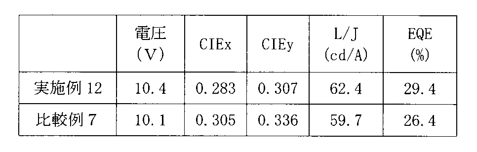
Claims (14)
- 陽極と、発光層と、障壁層と、電子注入層と、陰極とをこの順に備え、
前記発光層は、ホストと、主ピーク波長が550nm以下の蛍光発光を示すドーパントとを含み、
前記ドーパントのアフィニティAdが前記ホストのアフィニティAhより小さく、
前記ドーパントの3重項エネルギーET dが前記ホストの3重項エネルギーET hがより大きく、
前記障壁層の3重項エネルギーET bがET hより大きく、前記障壁層が炭化水素芳香族化合物からなる
有機エレクトロルミネッセンス素子。 - 前記陽極と発光層の間に正孔輸送帯域を備え、
前記正孔輸送帯域内に、前記発光層に隣接して正孔輸送層が設けられ、前記正孔輸送層の3重項エネルギーET hoがET hより大きい、
請求項1に記載の有機エレクトロルミネッセンス素子。 - 前記炭化水素芳香族環化合物が、多環芳香族化合物である請求項1又は2に記載の有機エレクトロルミネッセンス素子。
- 前記電子注入層を構成する材料が前記障壁層を構成する材料と同一である請求項1~3のいずれかに記載の有機エレクトロルミネッセンス素子。
- 前記電子注入層を構成する材料が前記障壁層を構成する材料と同一であり、かつ前記電子注入層にドナーがドープされている請求項1~3のいずれかに記載の有機エレクトロルミネッセンス素子。
- 前記ドーパントがピレン誘導体、アミノアントラセン誘導体、アミノクリセン誘導体、アミノピレン誘導体から選ばれる材料である請求項1~5のいずれかに記載の有機エレクトロルミネッセンス素子。
- 前記障壁層を構成する材料の電子移動度が、電界強度0.04~0.5MV/cmの範囲において、10-6cm2/Vs以上である請求項1~6のいずれかに記載の有機エレクトロルミネッセンス素子。
- 前記電子注入層を構成する材料の電子移動度が、電界強度0.04~0.5MV/cmの範囲において、10-6cm2/Vs以上である請求項1~7のいずれかに記載の有機エレクトロルミネッセンス素子。
- 前記障壁層のアフィニティAb、前記電子注入層のアフィニティAeがAe-Ab<0.2eVで表わされる関係を満たす請求項1~8のいずれかに記載の有機エレクトロルミネッセンス素子。
- 前記ホストが環式構造以外に二重結合を含まない化合物である請求項1~9のいずれかに記載の有機エレクトロルミネッセンス素子。
- 前記ドーパントが環式構造以外に二重結合を含まない化合物である請求項1~10のいずれかに記載の有機エレクトロルミネッセンス素子。
- 陽極と、発光層と、電子輸送帯域と、陰極とをこの順に備え、
前記発光層は、ホストと、主ピーク波長が550nm以下の蛍光発光を示すドーパントを含み、
前記ドーパントのアフィニティレベルAdが前記ホストのアフィニティレベルAhより小さく、
前記ドーパントの3重項エネルギーET dが前記ホストの3重項エネルギーET hがより大きく、
前記電子輸送帯域内に、前記発光層に隣接して障壁層が設けられ、前記障壁層を形成する材料の3重項エネルギーET bがET hより大きく、電流効率(単位:cd/A)が最大となる印加電圧において、前記発光層に生成する3重項励起子同士が衝突して生成する1重項励起子由来の発光強度が、全発光強度に対して30%以上である
有機エレクトロルミネッセンス素子。 - 前記陽極と前記陰極の間に2つ以上の発光層を有し、2つの発光層の間に中間層を備える請求項1~12のいずれかに記載の有機エレクトロルミネッセンス素子。
- 前記陽極と前記陰極の間に複数の発光層を含み、第一の発光層と第二の発光層の間に電荷障壁層を備える請求項1~12のいずれかに記載の有機エレクトロルミネッセンス素子。
Priority Applications (3)
| Application Number | Priority Date | Filing Date | Title |
|---|---|---|---|
| JP2011514346A JP5208271B2 (ja) | 2009-05-22 | 2010-05-21 | 有機エレクトロルミネッセンス素子 |
| CN201080021836XA CN102428589A (zh) | 2009-05-22 | 2010-05-21 | 有机电致发光元件 |
| EP10777588.4A EP2434559B1 (en) | 2009-05-22 | 2010-05-21 | Organic electroluminescent element |
Applications Claiming Priority (4)
| Application Number | Priority Date | Filing Date | Title |
|---|---|---|---|
| JP2009124760 | 2009-05-22 | ||
| JP2009-124760 | 2009-05-22 | ||
| JP2009125883 | 2009-05-25 | ||
| JP2009-125883 | 2009-05-25 |
Publications (1)
| Publication Number | Publication Date |
|---|---|
| WO2010134352A1 true WO2010134352A1 (ja) | 2010-11-25 |
Family
ID=43124136
Family Applications (1)
| Application Number | Title | Priority Date | Filing Date |
|---|---|---|---|
| PCT/JP2010/003434 WO2010134352A1 (ja) | 2009-05-22 | 2010-05-21 | 有機エレクトロルミネッセンス素子 |
Country Status (7)
| Country | Link |
|---|---|
| US (1) | US20100295445A1 (ja) |
| EP (1) | EP2434559B1 (ja) |
| JP (1) | JP5208271B2 (ja) |
| KR (1) | KR20120024624A (ja) |
| CN (1) | CN102428589A (ja) |
| TW (1) | TW201101922A (ja) |
| WO (1) | WO2010134352A1 (ja) |
Cited By (52)
| Publication number | Priority date | Publication date | Assignee | Title |
|---|---|---|---|---|
| JP2009016478A (ja) * | 2007-07-03 | 2009-01-22 | Canon Inc | 有機発光素子 |
| WO2011077689A1 (ja) * | 2009-12-21 | 2011-06-30 | 出光興産株式会社 | ピレン誘導体及びそれを用いた有機エレクトロルミネッセンス素子 |
| WO2012070234A1 (en) | 2010-11-22 | 2012-05-31 | Idemitsu Kosan Co.,Ltd. | Organic electroluminescence device |
| WO2012128090A1 (ja) * | 2011-03-24 | 2012-09-27 | パナソニック株式会社 | 有機エレクトロルミネッセンス素子 |
| JP2012186392A (ja) * | 2011-03-07 | 2012-09-27 | Seiko Epson Corp | 発光素子、発光装置、表示装置および電子機器 |
| WO2012133188A1 (ja) | 2011-03-25 | 2012-10-04 | 出光興産株式会社 | 有機エレクトロルミネッセンス素子 |
| EP2527334A1 (en) * | 2010-01-21 | 2012-11-28 | Idemitsu Kosan Co., Ltd. | Aromatic amine derivative, and organic electroluminescent element comprising same |
| JP2013062262A (ja) * | 2013-01-10 | 2013-04-04 | Panasonic Corp | 有機エレクトロルミネッセンス素子 |
| JP2013084620A (ja) * | 2013-01-10 | 2013-05-09 | Panasonic Corp | 有機エレクトロルミネッセンス素子 |
| WO2013118846A1 (ja) | 2012-02-10 | 2013-08-15 | 出光興産株式会社 | 芳香族アミン誘導体、有機エレクトロルミネッセンス素子及び電子機器 |
| WO2013180241A1 (ja) | 2012-06-01 | 2013-12-05 | 出光興産株式会社 | 有機エレクトロルミネッセンス素子および有機エレクトロルミネッセンス素子用材料 |
| JP2013247179A (ja) * | 2012-05-24 | 2013-12-09 | Udc Ireland Ltd | 有機電界発光素子、並びに該素子を用いた発光装置、表示装置及び照明装置 |
| JP2013251480A (ja) * | 2012-06-04 | 2013-12-12 | Udc Ireland Ltd | 有機電界発光素子用材料、有機電界発光素子並びに該素子を用いた発光装置、表示装置及び照明装置 |
| WO2014013947A1 (ja) | 2012-07-20 | 2014-01-23 | 出光興産株式会社 | 有機エレクトロルミネッセンス素子 |
| US8883323B2 (en) | 2010-11-22 | 2014-11-11 | Idemitsu Kosan Co., Ltd. | Organic electroluminescence device |
| WO2014199637A1 (ja) | 2013-06-11 | 2014-12-18 | 出光興産株式会社 | 有機エレクトロルミネッセンス素子用材料、これを用いた有機エレクトロルミネッセンス素子及び電子機器 |
| JP2015065152A (ja) * | 2013-06-28 | 2015-04-09 | 株式会社半導体エネルギー研究所 | 発光素子の作製方法及び発光素子 |
| JP2015065325A (ja) * | 2013-09-25 | 2015-04-09 | 出光興産株式会社 | 有機エレクトロルミネッセンス素子、および電子機器 |
| WO2015053403A1 (ja) | 2013-10-11 | 2015-04-16 | 出光興産株式会社 | 芳香族アミン化合物、有機エレクトロルミネッセンス素子及び電子機器 |
| WO2015072520A1 (ja) | 2013-11-13 | 2015-05-21 | 出光興産株式会社 | 化合物、有機エレクトロルミネッセンス素子用材料、有機エレクトロルミネッセンス素子および電子機器 |
| JP2015109407A (ja) * | 2013-05-16 | 2015-06-11 | 株式会社半導体エネルギー研究所 | 発光素子、発光装置、電子機器、および照明装置 |
| JP2015213059A (ja) * | 2014-04-18 | 2015-11-26 | 株式会社半導体エネルギー研究所 | 発光素子、発光装置、電子機器、および照明装置 |
| US9203043B2 (en) | 2012-05-28 | 2015-12-01 | Idemitsu Kosan Co., Ltd. | Organic electroluminescence device |
| US9258866B2 (en) | 2012-08-17 | 2016-02-09 | Idemitsu Kosan Co., Ltd. | Light-emitting device, electronic equipment, and method for producing light-emitting device |
| US9324950B2 (en) | 2010-11-22 | 2016-04-26 | Idemitsu Kosan Co., Ltd. | Organic electroluminescence device |
| JP2016110978A (ja) * | 2014-05-13 | 2016-06-20 | 株式会社半導体エネルギー研究所 | 発光素子、発光装置、表示装置、電子機器、および照明装置 |
| EP3147961A1 (en) | 2015-09-28 | 2017-03-29 | Novaled GmbH | Organic electroluminescent device |
| US9614170B2 (en) | 2012-10-03 | 2017-04-04 | Idemitsu Kosan Co., Ltd. | Organic electroluminescent element |
| US9647226B2 (en) | 2012-12-03 | 2017-05-09 | Idemitsu Kosan Co., Ltd. | Organic electroluminescent element |
| EP3182478A1 (en) | 2015-12-18 | 2017-06-21 | Novaled GmbH | Electron injection layer for an organic light-emitting diode (oled) |
| US9711732B2 (en) | 2012-03-29 | 2017-07-18 | Idemitsu Kosan Co., Ltd. | Organic electroluminescent element and material for organic electroluminescent elements |
| EP3211682A1 (en) | 2011-11-22 | 2017-08-30 | Idemitsu Kosan Co., Ltd | Aromatic heterocyclic derivative, organic electroluminescence device material and organic electroluminescence device field |
| US9768403B2 (en) | 2013-10-30 | 2017-09-19 | Sharp Kabushiki Kaisha | Organic electroluminescent element and organic electroluminescent display panel |
| EP3252841A1 (en) | 2016-05-30 | 2017-12-06 | Novaled GmbH | Organic light emitting diode comprising an organic semiconductor layer |
| EP3252837A1 (en) | 2016-05-30 | 2017-12-06 | Novaled GmbH | Organic light emitting diode comprising an organic semiconductor layer |
| WO2017221999A1 (en) | 2016-06-22 | 2017-12-28 | Idemitsu Kosan Co., Ltd. | Specifically substituted benzofuro- and benzothienoquinolines for organic light emitting diodes |
| US9966539B2 (en) | 2012-08-31 | 2018-05-08 | Idemitsu Kosan Co., Ltd. | Organic electroluminescence device |
| US9985233B2 (en) | 2015-12-01 | 2018-05-29 | Semiconductor Energy Laboratory Co., Ltd. | Light-emitting element having a delayed fluorescence component due to triplet-triplet annihilation |
| JP2018117164A (ja) * | 2011-04-29 | 2018-07-26 | 株式会社半導体エネルギー研究所 | 発光素子、発光装置、電子機器、照明装置 |
| US10128456B2 (en) | 2011-10-26 | 2018-11-13 | Idemitsu Kosan Co., Ltd. | Organic electroluminescence element, and material for organic electroluminescence element |
| US10135000B2 (en) | 2014-03-31 | 2018-11-20 | Idemitsu Kosan Co., Ltd. | Organic electroluminescent element and electronic device |
| WO2018212169A1 (ja) | 2017-05-16 | 2018-11-22 | 学校法人関西学院 | 多環芳香族化合物 |
| JP2018188444A (ja) * | 2010-04-09 | 2018-11-29 | 株式会社半導体エネルギー研究所 | 芳香族アミン誘導体、発光素子、発光装置、電子機器および照明装置 |
| KR20180133544A (ko) * | 2013-12-02 | 2018-12-14 | 가부시키가이샤 한도오따이 에네루기 켄큐쇼 | 발광 장치 |
| WO2019003615A1 (ja) | 2017-06-30 | 2019-01-03 | 学校法人関西学院 | 有機電界発光素子 |
| JP2019036739A (ja) * | 2011-03-30 | 2019-03-07 | 株式会社半導体エネルギー研究所 | 発光装置 |
| WO2020174305A1 (ja) * | 2019-02-26 | 2020-09-03 | 株式会社半導体エネルギー研究所 | 表示装置、表示モジュール、電子機器、及びテレビジョン装置 |
| WO2021065775A1 (ja) * | 2019-10-04 | 2021-04-08 | 出光興産株式会社 | 有機エレクトロルミネッセンス素子及び電子機器 |
| WO2021065774A1 (ja) * | 2019-10-04 | 2021-04-08 | 出光興産株式会社 | 有機エレクトロルミネッセンス素子及び電子機器 |
| US11189803B2 (en) | 2016-08-10 | 2021-11-30 | Idemitsu Kosan Co., Ltd. | Organic electroluminescent element and electronic device containing the organic electroluminescent element |
| WO2022230842A1 (ja) * | 2021-04-26 | 2022-11-03 | 出光興産株式会社 | 有機エレクトロルミネッセンス素子、有機エレクトロルミネッセンス表示装置及び電子機器 |
| US11730052B2 (en) | 2013-03-18 | 2023-08-15 | Idemitsu Kosan Co., Ltd. | Light-emitting device |
Families Citing this family (36)
| Publication number | Priority date | Publication date | Assignee | Title |
|---|---|---|---|---|
| US8154195B2 (en) * | 2007-07-07 | 2012-04-10 | Idemitsu Kosan Co., Ltd. | Organic electroluminescence device and material for organic electroluminescence device |
| CN101874316B (zh) | 2007-11-22 | 2012-09-05 | 出光兴产株式会社 | 有机el元件以及含有机el材料的溶液 |
| US8476823B2 (en) * | 2009-05-22 | 2013-07-02 | Idemitsu Kosan Co., Ltd. | Organic electroluminescent device |
| EP2441750A4 (en) | 2009-12-16 | 2012-12-12 | Idemitsu Kosan Co | AROMATIC AMINE DERIVATIVE AND ORGANIC ELECTROLUMINESCENT ELEMENT THEREWITH |
| CN102473857A (zh) * | 2010-01-15 | 2012-05-23 | 出光兴产株式会社 | 有机电致发光元件 |
| JP2011222831A (ja) * | 2010-04-12 | 2011-11-04 | Idemitsu Kosan Co Ltd | 有機エレクトロルミネッセンス素子 |
| WO2013039221A1 (ja) | 2011-09-16 | 2013-03-21 | 出光興産株式会社 | 芳香族アミン誘導体およびそれを用いた有機エレクトロルミネッセンス素子 |
| US10056558B2 (en) | 2011-11-25 | 2018-08-21 | Idemitsu Kosan Co., Ltd. | Aromatic amine derivative, material for organic electroluminescent element, and organic electroluminescent element |
| JP6060530B2 (ja) * | 2012-06-12 | 2017-01-18 | ソニー株式会社 | 有機電界発光素子及び表示装置 |
| JP6307686B2 (ja) | 2012-12-05 | 2018-04-11 | 三星ディスプレイ株式會社Samsung Display Co.,Ltd. | アミン誘導体、有機発光材料及びそれを用いた有機エレクトロルミネッセンス素子 |
| KR102050484B1 (ko) | 2013-03-04 | 2019-12-02 | 삼성디스플레이 주식회사 | 안트라센 유도체 및 이를 포함하는 유기전계발광소자 |
| KR102107106B1 (ko) | 2013-05-09 | 2020-05-07 | 삼성디스플레이 주식회사 | 스티릴계 화합물 및 이를 포함한 유기 발광 소자 |
| KR102269131B1 (ko) | 2013-07-01 | 2021-06-25 | 삼성디스플레이 주식회사 | 화합물 및 이를 포함한 유기 발광 소자 |
| DE112014005471B4 (de) | 2013-12-02 | 2022-10-06 | Semiconductor Energy Laboratory Co., Ltd. | Licht emittierendes Element, Licht emittierende Vorrichtung und Beleuchtungsvorrichtung |
| US10062850B2 (en) | 2013-12-12 | 2018-08-28 | Samsung Display Co., Ltd. | Amine-based compounds and organic light-emitting devices comprising the same |
| KR20150132795A (ko) | 2014-05-16 | 2015-11-26 | 삼성디스플레이 주식회사 | 유기 발광 소자 |
| KR102332591B1 (ko) | 2014-06-09 | 2021-11-30 | 삼성디스플레이 주식회사 | 유기 발광 소자 |
| KR102327086B1 (ko) | 2014-06-11 | 2021-11-17 | 삼성디스플레이 주식회사 | 유기 발광 소자 |
| JP6387311B2 (ja) * | 2014-06-26 | 2018-09-05 | 出光興産株式会社 | 有機エレクトロルミネッセンス素子、有機エレクトロルミネッセンス素子用材料、および電子機器 |
| TWI663173B (zh) | 2014-08-08 | 2019-06-21 | 愛爾蘭商Udc愛爾蘭責任有限公司 | 電致發光咪唑并喹噁啉碳烯金屬錯合物 |
| KR102287341B1 (ko) | 2014-08-19 | 2021-08-06 | 삼성디스플레이 주식회사 | 유기 발광 소자 및 이를 포함하는 유기 발광 표시 장치 |
| KR102384649B1 (ko) | 2014-11-10 | 2022-04-11 | 삼성디스플레이 주식회사 | 유기 발광 소자 |
| JP2016100364A (ja) | 2014-11-18 | 2016-05-30 | 三星ディスプレイ株式會社Samsung Display Co.,Ltd. | 有機エレクトロルミネッセンス素子用材料及びそれを用いた有機エレクトロルミネッセンス素子 |
| KR102385230B1 (ko) | 2014-11-19 | 2022-04-12 | 삼성디스플레이 주식회사 | 유기 발광 소자 |
| KR102363260B1 (ko) | 2014-12-19 | 2022-02-16 | 삼성디스플레이 주식회사 | 유기 발광 소자 |
| KR102343145B1 (ko) | 2015-01-12 | 2021-12-27 | 삼성디스플레이 주식회사 | 축합환 화합물 및 이를 포함한 유기 발광 소자 |
| US10062861B2 (en) | 2015-02-24 | 2018-08-28 | Semiconductor Energy Laboratory Co., Ltd. | Light-emitting element, display device, electronic device, and lighting device |
| CN104966786B (zh) * | 2015-07-03 | 2017-12-22 | 固安鼎材科技有限公司 | 一种有机电致发光器件 |
| KR102427671B1 (ko) | 2015-09-07 | 2022-08-02 | 삼성디스플레이 주식회사 | 유기 발광 소자 |
| KR102441556B1 (ko) | 2015-09-11 | 2022-09-08 | 삼성디스플레이 주식회사 | 화합물 및 이를 포함하는 유기 발광 소자 |
| KR102516053B1 (ko) | 2015-10-22 | 2023-03-31 | 삼성디스플레이 주식회사 | 화합물 및 이를 포함하는 유기 발광 소자 |
| KR20170074170A (ko) | 2015-12-21 | 2017-06-29 | 유디씨 아일랜드 리미티드 | 삼각형 리간드를 갖는 전이 금속 착체 및 oled에서의 이의 용도 |
| KR102528355B1 (ko) | 2016-05-11 | 2023-05-03 | 삼성디스플레이 주식회사 | 유기 발광 소자 및 이를 포함하는 발광 장치 |
| US20190386225A1 (en) * | 2017-02-14 | 2019-12-19 | Idemitsu Kosan Co., Ltd. | Novel compound, organic electroluminescent element using same, and electronic device |
| KR102395782B1 (ko) | 2017-07-31 | 2022-05-09 | 삼성전자주식회사 | 유기 발광 소자 |
| KR102083093B1 (ko) * | 2017-10-20 | 2020-02-28 | 주식회사 엘지화학 | 유기 발광 소자 |
Citations (34)
| Publication number | Priority date | Publication date | Assignee | Title |
|---|---|---|---|---|
| JPS6479297A (en) | 1987-09-22 | 1989-03-24 | Mitsubishi Heavy Ind Ltd | Apparatus for production of high-concentration coal-water slurry |
| JPH11345687A (ja) | 1998-06-01 | 1999-12-14 | Canon Inc | 発光素子 |
| JP2001357972A (ja) * | 2000-06-13 | 2001-12-26 | Hitachi Ltd | 有機電界発光素子 |
| WO2002014244A1 (fr) | 2000-08-10 | 2002-02-21 | Mitsui Chemicals, Inc. | Compose d'hydrocarbure, materiau pour element organique electroluminescent et element organique electroluminescent |
| JP2002100478A (ja) | 2000-09-20 | 2002-04-05 | Mitsubishi Chemicals Corp | 有機電界発光素子及びその製造方法 |
| JP2002525808A (ja) | 1998-09-14 | 2002-08-13 | ザ、トラスティーズ オブ プリンストン ユニバーシティ | 高効率の電界発光デバイスのための構造 |
| JP2003338377A (ja) | 2002-03-11 | 2003-11-28 | Tdk Corp | 有機el素子 |
| WO2004044088A1 (ja) | 2002-11-12 | 2004-05-27 | Idemitsu Kosan Co., Ltd. | 有機エレクトロルミネッセンス素子用材料及びそれを用いた有機エレクトロルミネッセンス素子 |
| JP2004204238A (ja) | 2002-12-24 | 2004-07-22 | Lg Electronics Inc | 有機電界発光デバイス |
| JP2004214180A (ja) | 2002-12-16 | 2004-07-29 | Canon Inc | 有機発光素子 |
| WO2004083162A1 (ja) | 2003-03-20 | 2004-09-30 | Idemitsu Kosan Co. Ltd. | 芳香族アミン誘導体及びそれを用いた有機エレクトロルミネッセンス素子 |
| JP2005072012A (ja) | 2003-08-27 | 2005-03-17 | Novaled Gmbh | 発光素子とその製造方法 |
| JP2005314239A (ja) | 2004-04-27 | 2005-11-10 | Mitsui Chemicals Inc | アントラセン化合物、および該アントラセン化合物を含有する有機電界発光素子 |
| WO2005108348A1 (ja) | 2004-05-12 | 2005-11-17 | Idemitsu Kosan Co., Ltd. | 芳香族アミン誘導体、それを用いた有機エレクトロルミネッセンス素子及び芳香族アミン誘導体の製造方法 |
| WO2005113531A1 (ja) | 2004-05-21 | 2005-12-01 | Toray Industries, Inc. | 発光素子材料および発光素子 |
| JP2005353288A (ja) * | 2004-06-08 | 2005-12-22 | Canon Inc | 有機発光素子 |
| US7018723B2 (en) | 2003-07-25 | 2006-03-28 | The University Of Southern California | Materials and structures for enhancing the performance of organic light emitting devices |
| JP2006278035A (ja) | 2005-03-28 | 2006-10-12 | Idemitsu Kosan Co Ltd | 発光分布推定方法、発光分布推定装置、発光分布推定プログラム、記録媒体、表示素子、画像表示装置 |
| WO2007021117A1 (en) | 2005-08-16 | 2007-02-22 | Gracel Display Inc. | Green electroluminescent compounds and organic electroluminescent device using the same |
| JP2007059903A (ja) * | 2005-08-25 | 2007-03-08 | Internatl Business Mach Corp <Ibm> | エレクトロルミネセンス・デバイス(光電子デバイスの安定性向上) |
| WO2007100010A1 (ja) | 2006-02-28 | 2007-09-07 | Idemitsu Kosan Co., Ltd. | 有機エレクトロルミネッセンス素子 |
| US20070273270A1 (en) | 2006-05-25 | 2007-11-29 | Idemitsu Kosan Co., Ltd. | Organic electroluminescence device |
| KR20070115588A (ko) | 2006-06-01 | 2007-12-06 | 에스에프씨 주식회사 | 청색발광화합물 및 이를 이용한 유기전계발광소자 |
| WO2008023623A1 (fr) | 2006-08-22 | 2008-02-28 | Idemitsu Kosan Co., Ltd. | Dispositif électroluminescent organique |
| JP2008506798A (ja) * | 2004-07-15 | 2008-03-06 | メルク パテント ゲーエムベーハー | アップコンバージョンのためのポリマーの使用、およびアップコンバージョンのためのデバイス |
| US7358661B2 (en) | 2003-04-24 | 2008-04-15 | Idemitsu Kosan Co., Ltd. | Organic electroluminescent device and display |
| WO2008062773A1 (fr) | 2006-11-20 | 2008-05-29 | Idemitsu Kosan Co., Ltd. | Dispositif électroluminescent organique |
| JP4134280B2 (ja) | 2006-05-25 | 2008-08-20 | 出光興産株式会社 | 有機エレクトロルミネッセンス素子及びフルカラー発光装置 |
| KR20080079956A (ko) | 2007-02-28 | 2008-09-02 | 에스에프씨 주식회사 | 청색발광화합물 및 이를 이용한 유기전계발광소자 |
| JP2008212102A (ja) | 2007-03-07 | 2008-09-18 | Mitsubishi Agricult Mach Co Ltd | コンバイン |
| WO2008145239A2 (de) | 2007-05-29 | 2008-12-04 | Merck Patent Gmbh | Benzanthracen-derivate für organische elektrolumineszenzvorrichtungen |
| JP2009090379A (ja) | 2007-10-03 | 2009-04-30 | Nakamura Tome Precision Ind Co Ltd | ドレス装置を備えた硬質脆性板の面取装置 |
| WO2009084512A1 (ja) | 2007-12-28 | 2009-07-09 | Idemitsu Kosan Co., Ltd. | 芳香族アミン誘導体及びそれを用いた有機エレクトロルミネッセンス素子 |
| KR20100024894A (ko) | 2008-08-26 | 2010-03-08 | 에스에프씨 주식회사 | 피렌계 화합물 및 이를 이용한 유기전계발광소자 |
Family Cites Families (10)
| Publication number | Priority date | Publication date | Assignee | Title |
|---|---|---|---|---|
| JPH1079297A (ja) * | 1996-07-09 | 1998-03-24 | Sony Corp | 電界発光素子 |
| US6830828B2 (en) * | 1998-09-14 | 2004-12-14 | The Trustees Of Princeton University | Organometallic complexes as phosphorescent emitters in organic LEDs |
| US7001536B2 (en) * | 1999-03-23 | 2006-02-21 | The Trustees Of Princeton University | Organometallic complexes as phosphorescent emitters in organic LEDs |
| US6660411B2 (en) * | 2000-09-20 | 2003-12-09 | Mitsubishi Chemical Corporation | Organic electroluminescent device |
| JP2005259492A (ja) * | 2004-03-11 | 2005-09-22 | Fuji Photo Film Co Ltd | 有機電界発光素子 |
| US9070884B2 (en) * | 2005-04-13 | 2015-06-30 | Universal Display Corporation | Hybrid OLED having phosphorescent and fluorescent emitters |
| EP2124270A4 (en) * | 2007-02-28 | 2010-08-25 | Idemitsu Kosan Co | ORGANIC EL-INSTALLATION |
| US20080284318A1 (en) * | 2007-05-17 | 2008-11-20 | Deaton Joseph C | Hybrid fluorescent/phosphorescent oleds |
| US20080286610A1 (en) * | 2007-05-17 | 2008-11-20 | Deaton Joseph C | Hybrid oled with fluorescent and phosphorescent layers |
| JPWO2009008344A1 (ja) * | 2007-07-07 | 2010-09-09 | 出光興産株式会社 | 有機el素子 |
-
2009
- 2009-06-04 US US12/478,290 patent/US20100295445A1/en not_active Abandoned
-
2010
- 2010-05-21 WO PCT/JP2010/003434 patent/WO2010134352A1/ja active Application Filing
- 2010-05-21 EP EP10777588.4A patent/EP2434559B1/en active Active
- 2010-05-21 KR KR1020117027666A patent/KR20120024624A/ko not_active Application Discontinuation
- 2010-05-21 CN CN201080021836XA patent/CN102428589A/zh active Pending
- 2010-05-21 JP JP2011514346A patent/JP5208271B2/ja active Active
- 2010-05-24 TW TW099116456A patent/TW201101922A/zh unknown
Patent Citations (34)
| Publication number | Priority date | Publication date | Assignee | Title |
|---|---|---|---|---|
| JPS6479297A (en) | 1987-09-22 | 1989-03-24 | Mitsubishi Heavy Ind Ltd | Apparatus for production of high-concentration coal-water slurry |
| JPH11345687A (ja) | 1998-06-01 | 1999-12-14 | Canon Inc | 発光素子 |
| JP2002525808A (ja) | 1998-09-14 | 2002-08-13 | ザ、トラスティーズ オブ プリンストン ユニバーシティ | 高効率の電界発光デバイスのための構造 |
| JP2001357972A (ja) * | 2000-06-13 | 2001-12-26 | Hitachi Ltd | 有機電界発光素子 |
| WO2002014244A1 (fr) | 2000-08-10 | 2002-02-21 | Mitsui Chemicals, Inc. | Compose d'hydrocarbure, materiau pour element organique electroluminescent et element organique electroluminescent |
| JP2002100478A (ja) | 2000-09-20 | 2002-04-05 | Mitsubishi Chemicals Corp | 有機電界発光素子及びその製造方法 |
| JP2003338377A (ja) | 2002-03-11 | 2003-11-28 | Tdk Corp | 有機el素子 |
| WO2004044088A1 (ja) | 2002-11-12 | 2004-05-27 | Idemitsu Kosan Co., Ltd. | 有機エレクトロルミネッセンス素子用材料及びそれを用いた有機エレクトロルミネッセンス素子 |
| JP2004214180A (ja) | 2002-12-16 | 2004-07-29 | Canon Inc | 有機発光素子 |
| JP2004204238A (ja) | 2002-12-24 | 2004-07-22 | Lg Electronics Inc | 有機電界発光デバイス |
| WO2004083162A1 (ja) | 2003-03-20 | 2004-09-30 | Idemitsu Kosan Co. Ltd. | 芳香族アミン誘導体及びそれを用いた有機エレクトロルミネッセンス素子 |
| US7358661B2 (en) | 2003-04-24 | 2008-04-15 | Idemitsu Kosan Co., Ltd. | Organic electroluminescent device and display |
| US7018723B2 (en) | 2003-07-25 | 2006-03-28 | The University Of Southern California | Materials and structures for enhancing the performance of organic light emitting devices |
| JP2005072012A (ja) | 2003-08-27 | 2005-03-17 | Novaled Gmbh | 発光素子とその製造方法 |
| JP2005314239A (ja) | 2004-04-27 | 2005-11-10 | Mitsui Chemicals Inc | アントラセン化合物、および該アントラセン化合物を含有する有機電界発光素子 |
| WO2005108348A1 (ja) | 2004-05-12 | 2005-11-17 | Idemitsu Kosan Co., Ltd. | 芳香族アミン誘導体、それを用いた有機エレクトロルミネッセンス素子及び芳香族アミン誘導体の製造方法 |
| WO2005113531A1 (ja) | 2004-05-21 | 2005-12-01 | Toray Industries, Inc. | 発光素子材料および発光素子 |
| JP2005353288A (ja) * | 2004-06-08 | 2005-12-22 | Canon Inc | 有機発光素子 |
| JP2008506798A (ja) * | 2004-07-15 | 2008-03-06 | メルク パテント ゲーエムベーハー | アップコンバージョンのためのポリマーの使用、およびアップコンバージョンのためのデバイス |
| JP2006278035A (ja) | 2005-03-28 | 2006-10-12 | Idemitsu Kosan Co Ltd | 発光分布推定方法、発光分布推定装置、発光分布推定プログラム、記録媒体、表示素子、画像表示装置 |
| WO2007021117A1 (en) | 2005-08-16 | 2007-02-22 | Gracel Display Inc. | Green electroluminescent compounds and organic electroluminescent device using the same |
| JP2007059903A (ja) * | 2005-08-25 | 2007-03-08 | Internatl Business Mach Corp <Ibm> | エレクトロルミネセンス・デバイス(光電子デバイスの安定性向上) |
| WO2007100010A1 (ja) | 2006-02-28 | 2007-09-07 | Idemitsu Kosan Co., Ltd. | 有機エレクトロルミネッセンス素子 |
| US20070273270A1 (en) | 2006-05-25 | 2007-11-29 | Idemitsu Kosan Co., Ltd. | Organic electroluminescence device |
| JP4134280B2 (ja) | 2006-05-25 | 2008-08-20 | 出光興産株式会社 | 有機エレクトロルミネッセンス素子及びフルカラー発光装置 |
| KR20070115588A (ko) | 2006-06-01 | 2007-12-06 | 에스에프씨 주식회사 | 청색발광화합물 및 이를 이용한 유기전계발광소자 |
| WO2008023623A1 (fr) | 2006-08-22 | 2008-02-28 | Idemitsu Kosan Co., Ltd. | Dispositif électroluminescent organique |
| WO2008062773A1 (fr) | 2006-11-20 | 2008-05-29 | Idemitsu Kosan Co., Ltd. | Dispositif électroluminescent organique |
| KR20080079956A (ko) | 2007-02-28 | 2008-09-02 | 에스에프씨 주식회사 | 청색발광화합물 및 이를 이용한 유기전계발광소자 |
| JP2008212102A (ja) | 2007-03-07 | 2008-09-18 | Mitsubishi Agricult Mach Co Ltd | コンバイン |
| WO2008145239A2 (de) | 2007-05-29 | 2008-12-04 | Merck Patent Gmbh | Benzanthracen-derivate für organische elektrolumineszenzvorrichtungen |
| JP2009090379A (ja) | 2007-10-03 | 2009-04-30 | Nakamura Tome Precision Ind Co Ltd | ドレス装置を備えた硬質脆性板の面取装置 |
| WO2009084512A1 (ja) | 2007-12-28 | 2009-07-09 | Idemitsu Kosan Co., Ltd. | 芳香族アミン誘導体及びそれを用いた有機エレクトロルミネッセンス素子 |
| KR20100024894A (ko) | 2008-08-26 | 2010-03-08 | 에스에프씨 주식회사 | 피렌계 화합물 및 이를 이용한 유기전계발광소자 |
Non-Patent Citations (10)
| Title |
|---|
| BERNHARD NICKEL ET AL.: "DELAYED FLUORESCENCE FROM THE LOWEST1B+3mum'' STATE OF ANTHRACENE, DUE TO HETERO-TRIPLET-TRIPLET ANNIHILATION OF 3ANTHRACENE AND 3XANTHONE", CHEMICAL PHYSICS, 1982, pages 365 - 376, XP008149484 * |
| CHIMED GANZORIG ET AL.: "A possible mechanism for enhanced electrofluoresecence emission through triplet-triplet annihilation in organic electroluminescent devices", APPLIED PHYSICS LETTERS, vol. 81, no. 17, 21 October 2002 (2002-10-21), pages 3137 - 3139, XP012032244 * |
| CHIMED GANZORIG ET AL.: "Evidence for enhanced electrofluorescence emission through triplet-triplet annihilation in organic electroluminescent devices", DAI 49 KAI EXTENDED ABSTRACTS, JAPAN SOCIETY OF APPLIED PHYSICS AND RELATED SOCIETIES, March 2002 (2002-03-01), pages 1314 - 28A-YE-4, XP008166764 * |
| D.V.KONDAKOV ET AL.: "Triplet annihilation exceeding spin statistical limit in highly efficient fluorescent organic light-emitting diodes", JOURNAL OF APPLIED PHYSICS, vol. 106, 2009, pages 124510, XP012127460 * |
| D.Y.KONDAKOV: "Characterization of triplet-triplet annihilation in organic light-emitting diodes based on anthracene derivatives", JOURNAL OF APPLIED PHYSICS, vol. 102, 2007, pages 114504, XP012105139 * |
| JOURNAL OF APPLIED PHYSICS, vol. 102, 2007, pages 114504 |
| S.M. BACHILO ET AL., J. PHYS. CHEM. A, vol. 104, 2000, pages 7711 |
| See also references of EP2434559A4 |
| SHIZUO TOKITO: "Yuki EL Device no Ko Koritsuka", THE CHEMICAL TIMES, no. 2, 2010, pages 5, XP008149511 * |
| SID 2008 DIGEST, 2008, pages 709 |
Cited By (101)
| Publication number | Priority date | Publication date | Assignee | Title |
|---|---|---|---|---|
| JP2009016478A (ja) * | 2007-07-03 | 2009-01-22 | Canon Inc | 有機発光素子 |
| WO2011077689A1 (ja) * | 2009-12-21 | 2011-06-30 | 出光興産株式会社 | ピレン誘導体及びそれを用いた有機エレクトロルミネッセンス素子 |
| EP2527334A4 (en) * | 2010-01-21 | 2013-10-16 | Idemitsu Kosan Co | AROMATIC AMINE DERIVATIVE AND ORGANIC ELECTROLUMINESCENT ELEMENT THEREWITH |
| EP2527334A1 (en) * | 2010-01-21 | 2012-11-28 | Idemitsu Kosan Co., Ltd. | Aromatic amine derivative, and organic electroluminescent element comprising same |
| JP2019052151A (ja) * | 2010-04-09 | 2019-04-04 | 株式会社半導体エネルギー研究所 | 化合物 |
| US11046667B2 (en) | 2010-04-09 | 2021-06-29 | Semiconductor Energy Laboratory Co., Ltd. | Aromatic amine derivative, light-emitting element, light-emitting device, electronic device, and lighting device |
| US10570113B2 (en) | 2010-04-09 | 2020-02-25 | Semiconductor Energy Laboratory Co., Ltd. | Aromatic amine derivative, light-emitting element, light-emitting device, electronic device, and lighting device |
| JP2018188444A (ja) * | 2010-04-09 | 2018-11-29 | 株式会社半導体エネルギー研究所 | 芳香族アミン誘導体、発光素子、発光装置、電子機器および照明装置 |
| US9324950B2 (en) | 2010-11-22 | 2016-04-26 | Idemitsu Kosan Co., Ltd. | Organic electroluminescence device |
| WO2012070233A1 (en) | 2010-11-22 | 2012-05-31 | Idemitsu Kosan Co.,Ltd. | Organic electroluminescence device |
| US8883323B2 (en) | 2010-11-22 | 2014-11-11 | Idemitsu Kosan Co., Ltd. | Organic electroluminescence device |
| WO2012070234A1 (en) | 2010-11-22 | 2012-05-31 | Idemitsu Kosan Co.,Ltd. | Organic electroluminescence device |
| JP2012186392A (ja) * | 2011-03-07 | 2012-09-27 | Seiko Epson Corp | 発光素子、発光装置、表示装置および電子機器 |
| US8941102B2 (en) | 2011-03-24 | 2015-01-27 | Panasonic Intellectual Property Management Co., Ltd. | Organic electroluminescent element |
| DE112012001399T5 (de) | 2011-03-24 | 2013-12-19 | Panasonic Corporation | Organisches Elektrolumineszenzelement |
| WO2012128090A1 (ja) * | 2011-03-24 | 2012-09-27 | パナソニック株式会社 | 有機エレクトロルミネッセンス素子 |
| JP2012204096A (ja) * | 2011-03-24 | 2012-10-22 | Panasonic Corp | 有機エレクトロルミネッセンス素子 |
| WO2012133188A1 (ja) | 2011-03-25 | 2012-10-04 | 出光興産株式会社 | 有機エレクトロルミネッセンス素子 |
| EP3598520A1 (en) | 2011-03-25 | 2020-01-22 | Idemitsu Kosan Co., Ltd | Organic electroluminescent element |
| US8643268B2 (en) | 2011-03-25 | 2014-02-04 | Idemitsu Kosan Co., Ltd. | Organic electroluminescence device |
| US10879482B2 (en) | 2011-03-25 | 2020-12-29 | Idemitsu Kosan Co., Ltd. | Organic electroluminescence device |
| JP2019036739A (ja) * | 2011-03-30 | 2019-03-07 | 株式会社半導体エネルギー研究所 | 発光装置 |
| JP2018117164A (ja) * | 2011-04-29 | 2018-07-26 | 株式会社半導体エネルギー研究所 | 発光素子、発光装置、電子機器、照明装置 |
| US10128456B2 (en) | 2011-10-26 | 2018-11-13 | Idemitsu Kosan Co., Ltd. | Organic electroluminescence element, and material for organic electroluminescence element |
| US10707434B2 (en) | 2011-10-26 | 2020-07-07 | Idemitsu Kosan Co., Ltd. | Organic electroluminescence element, and material for organic electroluminescence element |
| EP3211682A1 (en) | 2011-11-22 | 2017-08-30 | Idemitsu Kosan Co., Ltd | Aromatic heterocyclic derivative, organic electroluminescence device material and organic electroluminescence device field |
| US9871203B2 (en) | 2012-02-10 | 2018-01-16 | Idemitsu Kosan Co., Ltd. | Aromatic amine derivative, organic electroluminescent element and electronic device |
| WO2013118846A1 (ja) | 2012-02-10 | 2013-08-15 | 出光興産株式会社 | 芳香族アミン誘導体、有機エレクトロルミネッセンス素子及び電子機器 |
| US9711732B2 (en) | 2012-03-29 | 2017-07-18 | Idemitsu Kosan Co., Ltd. | Organic electroluminescent element and material for organic electroluminescent elements |
| JP2013247179A (ja) * | 2012-05-24 | 2013-12-09 | Udc Ireland Ltd | 有機電界発光素子、並びに該素子を用いた発光装置、表示装置及び照明装置 |
| US9203043B2 (en) | 2012-05-28 | 2015-12-01 | Idemitsu Kosan Co., Ltd. | Organic electroluminescence device |
| USRE46974E1 (en) | 2012-05-28 | 2018-07-31 | Idemitsu Kosan Co., Ltd. | Organic electroluminescence device |
| US9099658B2 (en) | 2012-06-01 | 2015-08-04 | Idemitsu Kosan Co., Ltd. | Organic electroluminescence device |
| USRE49343E1 (en) | 2012-06-01 | 2022-12-20 | Idemitsu Kosan Co., Ltd. | Organic electroluminescence device |
| EP3809482A2 (en) | 2012-06-01 | 2021-04-21 | Idemitsu Kosan Co.,Ltd. | Organic electroluminescence element and material for organic electroluminescence element |
| WO2013180241A1 (ja) | 2012-06-01 | 2013-12-05 | 出光興産株式会社 | 有機エレクトロルミネッセンス素子および有機エレクトロルミネッセンス素子用材料 |
| JP2013251480A (ja) * | 2012-06-04 | 2013-12-12 | Udc Ireland Ltd | 有機電界発光素子用材料、有機電界発光素子並びに該素子を用いた発光装置、表示装置及び照明装置 |
| US10461264B2 (en) | 2012-07-20 | 2019-10-29 | Idemitsu Kosan Co., Ltd. | Organic electroluminescent element |
| WO2014013947A1 (ja) | 2012-07-20 | 2014-01-23 | 出光興産株式会社 | 有機エレクトロルミネッセンス素子 |
| US9219242B2 (en) | 2012-07-20 | 2015-12-22 | Idemitsu Kosan Co., Ltd. | Organic electroluminescent element |
| EP3249711A1 (en) | 2012-07-20 | 2017-11-29 | Idemitsu Kosan Co., Ltd. | Organic electroluminescent element |
| US9608209B2 (en) | 2012-07-20 | 2017-03-28 | Idemitsu Kosan Co., Ltd. | Organic electroluminescent element |
| US10930860B2 (en) | 2012-07-20 | 2021-02-23 | Idemitsu Kosan Co., Ltd. | Organic electroluminescent element |
| US10032998B2 (en) | 2012-07-20 | 2018-07-24 | Idemitsu Kosan Co., Ltd. | Organic electroluminescent element |
| US9258866B2 (en) | 2012-08-17 | 2016-02-09 | Idemitsu Kosan Co., Ltd. | Light-emitting device, electronic equipment, and method for producing light-emitting device |
| US9966539B2 (en) | 2012-08-31 | 2018-05-08 | Idemitsu Kosan Co., Ltd. | Organic electroluminescence device |
| US9614170B2 (en) | 2012-10-03 | 2017-04-04 | Idemitsu Kosan Co., Ltd. | Organic electroluminescent element |
| US9899620B2 (en) | 2012-10-03 | 2018-02-20 | Idemitsu Kosan Co. Ltd. | Organic electroluminescent element |
| US9647226B2 (en) | 2012-12-03 | 2017-05-09 | Idemitsu Kosan Co., Ltd. | Organic electroluminescent element |
| JP2013062262A (ja) * | 2013-01-10 | 2013-04-04 | Panasonic Corp | 有機エレクトロルミネッセンス素子 |
| JP2013084620A (ja) * | 2013-01-10 | 2013-05-09 | Panasonic Corp | 有機エレクトロルミネッセンス素子 |
| US11730052B2 (en) | 2013-03-18 | 2023-08-15 | Idemitsu Kosan Co., Ltd. | Light-emitting device |
| US10128455B2 (en) | 2013-05-16 | 2018-11-13 | Semiconductor Energy Laboratory Co., Ltd. | Light-emitting element, light-emitting device, electronic device, and lighting device |
| JP2015109407A (ja) * | 2013-05-16 | 2015-06-11 | 株式会社半導体エネルギー研究所 | 発光素子、発光装置、電子機器、および照明装置 |
| JP7232868B2 (ja) | 2013-05-16 | 2023-03-03 | 株式会社半導体エネルギー研究所 | 発光素子 |
| JP2019216288A (ja) * | 2013-05-16 | 2019-12-19 | 株式会社半導体エネルギー研究所 | 発光素子 |
| JP2021121041A (ja) * | 2013-05-16 | 2021-08-19 | 株式会社半導体エネルギー研究所 | 発光素子 |
| US11462701B2 (en) | 2013-05-16 | 2022-10-04 | Semiconductor Energy Laboratory Co., Ltd. | Light-emitting element, light-emitting device, electronic device, and lighting device |
| WO2014199637A1 (ja) | 2013-06-11 | 2014-12-18 | 出光興産株式会社 | 有機エレクトロルミネッセンス素子用材料、これを用いた有機エレクトロルミネッセンス素子及び電子機器 |
| US10121969B2 (en) | 2013-06-28 | 2018-11-06 | Semiconductor Energy Laboratory Co., Ltd. | Method for fabricating light-emitting element using chamber with mass spectrometer |
| JP2015065152A (ja) * | 2013-06-28 | 2015-04-09 | 株式会社半導体エネルギー研究所 | 発光素子の作製方法及び発光素子 |
| JP2015065325A (ja) * | 2013-09-25 | 2015-04-09 | 出光興産株式会社 | 有機エレクトロルミネッセンス素子、および電子機器 |
| WO2015053403A1 (ja) | 2013-10-11 | 2015-04-16 | 出光興産株式会社 | 芳香族アミン化合物、有機エレクトロルミネッセンス素子及び電子機器 |
| EP4345089A2 (en) | 2013-10-11 | 2024-04-03 | Idemitsu Kosan Co.,Ltd. | Aromatic amine compound, organic electroluminescent element and electronic device |
| US9768403B2 (en) | 2013-10-30 | 2017-09-19 | Sharp Kabushiki Kaisha | Organic electroluminescent element and organic electroluminescent display panel |
| WO2015072520A1 (ja) | 2013-11-13 | 2015-05-21 | 出光興産株式会社 | 化合物、有機エレクトロルミネッセンス素子用材料、有機エレクトロルミネッセンス素子および電子機器 |
| US10217954B2 (en) | 2013-11-13 | 2019-02-26 | Idemitsu Kosan Co., Ltd. | Compound, material for organic electroluminescent element, organic electroluminescent element, and electronic device |
| US11672136B2 (en) | 2013-12-02 | 2023-06-06 | Semiconductor Energy Laboratory Co., Ltd. | Light-emitting element, display module, lighting module, light-emitting device, display device, electronic appliance, and lighting device |
| JP2019062211A (ja) * | 2013-12-02 | 2019-04-18 | 株式会社半導体エネルギー研究所 | 発光装置 |
| KR20180133544A (ko) * | 2013-12-02 | 2018-12-14 | 가부시키가이샤 한도오따이 에네루기 켄큐쇼 | 발광 장치 |
| JP2022082817A (ja) * | 2013-12-02 | 2022-06-02 | 株式会社半導体エネルギー研究所 | 発光装置 |
| US10930873B2 (en) | 2013-12-02 | 2021-02-23 | Semiconductor Energy Laboratory Co., Ltd. | Light-emitting element, display module, lighting module, light-emitting device, display device, electronic appliance, and lighting device |
| US10374186B2 (en) | 2013-12-02 | 2019-08-06 | Semiconductor Energy Laboratory Co., Ltd. | Light-emitting element, display module, lighting module, light-emitting device, display device, electronic appliance, and lighting device |
| KR102138453B1 (ko) * | 2013-12-02 | 2020-07-27 | 가부시키가이샤 한도오따이 에네루기 켄큐쇼 | 발광 장치 |
| JP2019175870A (ja) * | 2013-12-02 | 2019-10-10 | 株式会社半導体エネルギー研究所 | 発光装置 |
| US10135000B2 (en) | 2014-03-31 | 2018-11-20 | Idemitsu Kosan Co., Ltd. | Organic electroluminescent element and electronic device |
| JP2015213059A (ja) * | 2014-04-18 | 2015-11-26 | 株式会社半導体エネルギー研究所 | 発光素子、発光装置、電子機器、および照明装置 |
| US10686153B2 (en) | 2014-05-13 | 2020-06-16 | Semiconductor Energy Laboratory Co., Ltd. | Exciplex light-emitting device |
| JP2020043350A (ja) * | 2014-05-13 | 2020-03-19 | 株式会社半導体エネルギー研究所 | 発光素子、発光装置、モジュール、電子機器、および照明装置 |
| JP2020043351A (ja) * | 2014-05-13 | 2020-03-19 | 株式会社半導体エネルギー研究所 | 発光装置 |
| JP2019024140A (ja) * | 2014-05-13 | 2019-02-14 | 株式会社半導体エネルギー研究所 | 発光装置 |
| JP2016110978A (ja) * | 2014-05-13 | 2016-06-20 | 株式会社半導体エネルギー研究所 | 発光素子、発光装置、表示装置、電子機器、および照明装置 |
| US11864403B2 (en) | 2014-05-13 | 2024-01-02 | Semiconductor Energy Laboratory Co., Ltd. | Light-emitting device comprising first to third light-emitting layers |
| US11158832B2 (en) | 2014-05-13 | 2021-10-26 | Semiconductor Energy Laboratory Co., Ltd. | Light-emitting device with exciplex light-emitting layers |
| EP3147961A1 (en) | 2015-09-28 | 2017-03-29 | Novaled GmbH | Organic electroluminescent device |
| US10573837B2 (en) | 2015-12-01 | 2020-02-25 | Semiconductor Energy Laboratory Co., Ltd. | Light-emitting element |
| US11050032B2 (en) | 2015-12-01 | 2021-06-29 | Semiconductor Energy Laboratory Co., Ltd. | Light-emitting element |
| JP2022009708A (ja) * | 2015-12-01 | 2022-01-14 | 株式会社半導体エネルギー研究所 | 発光素子、発光装置、電子機器および照明装置 |
| US9985233B2 (en) | 2015-12-01 | 2018-05-29 | Semiconductor Energy Laboratory Co., Ltd. | Light-emitting element having a delayed fluorescence component due to triplet-triplet annihilation |
| JP7269305B2 (ja) | 2015-12-01 | 2023-05-08 | 株式会社半導体エネルギー研究所 | 発光素子、発光装置、電子機器および照明装置 |
| EP3182478A1 (en) | 2015-12-18 | 2017-06-21 | Novaled GmbH | Electron injection layer for an organic light-emitting diode (oled) |
| EP3252837A1 (en) | 2016-05-30 | 2017-12-06 | Novaled GmbH | Organic light emitting diode comprising an organic semiconductor layer |
| EP3252841A1 (en) | 2016-05-30 | 2017-12-06 | Novaled GmbH | Organic light emitting diode comprising an organic semiconductor layer |
| WO2017221999A1 (en) | 2016-06-22 | 2017-12-28 | Idemitsu Kosan Co., Ltd. | Specifically substituted benzofuro- and benzothienoquinolines for organic light emitting diodes |
| US11189803B2 (en) | 2016-08-10 | 2021-11-30 | Idemitsu Kosan Co., Ltd. | Organic electroluminescent element and electronic device containing the organic electroluminescent element |
| WO2018212169A1 (ja) | 2017-05-16 | 2018-11-22 | 学校法人関西学院 | 多環芳香族化合物 |
| WO2019003615A1 (ja) | 2017-06-30 | 2019-01-03 | 学校法人関西学院 | 有機電界発光素子 |
| WO2020174305A1 (ja) * | 2019-02-26 | 2020-09-03 | 株式会社半導体エネルギー研究所 | 表示装置、表示モジュール、電子機器、及びテレビジョン装置 |
| WO2021065775A1 (ja) * | 2019-10-04 | 2021-04-08 | 出光興産株式会社 | 有機エレクトロルミネッセンス素子及び電子機器 |
| WO2021065774A1 (ja) * | 2019-10-04 | 2021-04-08 | 出光興産株式会社 | 有機エレクトロルミネッセンス素子及び電子機器 |
| WO2022230842A1 (ja) * | 2021-04-26 | 2022-11-03 | 出光興産株式会社 | 有機エレクトロルミネッセンス素子、有機エレクトロルミネッセンス表示装置及び電子機器 |
Also Published As
| Publication number | Publication date |
|---|---|
| KR20120024624A (ko) | 2012-03-14 |
| CN102428589A (zh) | 2012-04-25 |
| EP2434559A1 (en) | 2012-03-28 |
| JP5208271B2 (ja) | 2013-06-12 |
| EP2434559B1 (en) | 2018-04-18 |
| JPWO2010134352A1 (ja) | 2012-11-08 |
| EP2434559A4 (en) | 2013-04-24 |
| US20100295445A1 (en) | 2010-11-25 |
| TW201101922A (en) | 2011-01-01 |
Similar Documents
| Publication | Publication Date | Title |
|---|---|---|
| JP5208271B2 (ja) | 有機エレクトロルミネッセンス素子 | |
| JP5208270B2 (ja) | 有機エレクトロルミネッセンス素子 | |
| US9153790B2 (en) | Organic electroluminescent device | |
| US9812661B2 (en) | Organic electroluminescent device | |
| JP5405653B1 (ja) | 有機エレクトロルミネッセンス素子 | |
| US9324950B2 (en) | Organic electroluminescence device | |
| JP6619021B2 (ja) | 発光素子並びに発光方法 | |
| US8883323B2 (en) | Organic electroluminescence device | |
| US20120126205A1 (en) | Organic electroluminescence device | |
| EP2133932A1 (en) | Organic el device | |
| EP2166588A1 (en) | Organic el device | |
| EP2166591A1 (en) | Organic el device | |
| JPWO2009008346A1 (ja) | 有機el素子 | |
| WO2012070227A1 (ja) | 有機エレクトロルミネッセンス素子 |
Legal Events
| Date | Code | Title | Description |
|---|---|---|---|
| WWE | Wipo information: entry into national phase |
Ref document number: 201080021836.X Country of ref document: CN |
|
| 121 | Ep: the epo has been informed by wipo that ep was designated in this application |
Ref document number: 10777588 Country of ref document: EP Kind code of ref document: A1 |
|
| WWE | Wipo information: entry into national phase |
Ref document number: 2011514346 Country of ref document: JP |
|
| WWE | Wipo information: entry into national phase |
Ref document number: 2010777588 Country of ref document: EP |
|
| ENP | Entry into the national phase |
Ref document number: 20117027666 Country of ref document: KR Kind code of ref document: A |
|
| NENP | Non-entry into the national phase |
Ref country code: DE |