US9966539B2 - Organic electroluminescence device - Google Patents
Organic electroluminescence device Download PDFInfo
- Publication number
- US9966539B2 US9966539B2 US13/767,417 US201313767417A US9966539B2 US 9966539 B2 US9966539 B2 US 9966539B2 US 201313767417 A US201313767417 A US 201313767417A US 9966539 B2 US9966539 B2 US 9966539B2
- Authority
- US
- United States
- Prior art keywords
- carbon atoms
- group
- substituted
- ring carbon
- unsubstituted
- Prior art date
- Legal status (The legal status is an assumption and is not a legal conclusion. Google has not performed a legal analysis and makes no representation as to the accuracy of the status listed.)
- Active, expires
Links
- 0 [1*]C1([2*])C2=CC(CN(C)C)=CC=C2C2=CC=C(CN(C)C)C=C21 Chemical compound [1*]C1([2*])C2=CC(CN(C)C)=CC=C2C2=CC=C(CN(C)C)C=C21 0.000 description 23
- DPUCNQRJRFYWGA-UHFFFAOYSA-N C1=CC2=C(C=C1)C1=C(C=CC=C1)C2.CC.CC.CC.CC.CC.CC.CCC.CCC.CCN1C2=C(C=CC=C2)C2=C1/C=C\C=C/2.CN1C2=C(C=CC=C2)C2=C1C=CC=C2 Chemical compound C1=CC2=C(C=C1)C1=C(C=CC=C1)C2.CC.CC.CC.CC.CC.CC.CCC.CCC.CCN1C2=C(C=CC=C2)C2=C1/C=C\C=C/2.CN1C2=C(C=CC=C2)C2=C1C=CC=C2 DPUCNQRJRFYWGA-UHFFFAOYSA-N 0.000 description 4
- ZHQZMZPTWFUIOB-UHFFFAOYSA-N C1=CC=CC=C1.C1=CC=CC=C1.C1=CC=CC=C1.C1=CC=CC=C1.C1=CC=CC=C1.C1=CC=CC=C1.C1=CC=CC=C1.C1=CC=CC=C1.C1=CC=CC=C1.CC.CC.CC.CC.CC.CC.CC.CC.CC.CC.CC.CC.CC.CC.CC.CC.CC.CC Chemical compound C1=CC=CC=C1.C1=CC=CC=C1.C1=CC=CC=C1.C1=CC=CC=C1.C1=CC=CC=C1.C1=CC=CC=C1.C1=CC=CC=C1.C1=CC=CC=C1.C1=CC=CC=C1.CC.CC.CC.CC.CC.CC.CC.CC.CC.CC.CC.CC.CC.CC.CC.CC.CC.CC ZHQZMZPTWFUIOB-UHFFFAOYSA-N 0.000 description 4
- GETQZCLCWQTVFV-UHFFFAOYSA-N CN(C)C Chemical compound CN(C)C GETQZCLCWQTVFV-UHFFFAOYSA-N 0.000 description 4
- VTSAYWZCLNPTGP-UHFFFAOYSA-N C1=CC=C(C2=CC=C(C3=CC=C(N(C4=CC=C(C5=CC=CC6=C5OC5=C6C=CC=C5)C=C4)C4=CC=C(C5=C6OC7=C(C=CC=C7)C6=CC=C5)C=C4)C=C3)C=C2)C=C1 Chemical compound C1=CC=C(C2=CC=C(C3=CC=C(N(C4=CC=C(C5=CC=CC6=C5OC5=C6C=CC=C5)C=C4)C4=CC=C(C5=C6OC7=C(C=CC=C7)C6=CC=C5)C=C4)C=C3)C=C2)C=C1 VTSAYWZCLNPTGP-UHFFFAOYSA-N 0.000 description 3
- BQFIIADCVFHAKC-UHFFFAOYSA-N C1=CC=C(C2=CC=C(C3=CC(C4=CC(N5C6=C(C=CC=C6)C6=C5C=CC=C6)=CC(N5C6=C(C=CC=C6)C6=C5C=CC=C6)=C4)=NC(C4=CC=CC=C4)=N3)C=C2)C=C1 Chemical compound C1=CC=C(C2=CC=C(C3=CC(C4=CC(N5C6=C(C=CC=C6)C6=C5C=CC=C6)=CC(N5C6=C(C=CC=C6)C6=C5C=CC=C6)=C4)=NC(C4=CC=CC=C4)=N3)C=C2)C=C1 BQFIIADCVFHAKC-UHFFFAOYSA-N 0.000 description 2
- MWMTXZXGLJUSAJ-UHFFFAOYSA-N CC1(C)C2=CC(N(C3=CC=CC=C3)C3=CC=C(C4=CC=CC=C4)C=C3)=CC=C2C2=C1/C=C(N(C1=CC=CC=C1)C1=CC=C(C3=CC=CC=C3)C=C1)/C=C\2 Chemical compound CC1(C)C2=CC(N(C3=CC=CC=C3)C3=CC=C(C4=CC=CC=C4)C=C3)=CC=C2C2=C1/C=C(N(C1=CC=CC=C1)C1=CC=C(C3=CC=CC=C3)C=C1)/C=C\2 MWMTXZXGLJUSAJ-UHFFFAOYSA-N 0.000 description 2
- BRAHEWAYJMQHNE-UHFFFAOYSA-N CCC1=NC2=C(C=CC=C2)N1C1=CC=C(C2=C3C=CC=CC3=C(C3=CC=C(C4=CC=CC=C4)C=C3)C3=C2C=CC=C3)C=C1 Chemical compound CCC1=NC2=C(C=CC=C2)N1C1=CC=C(C2=C3C=CC=CC3=C(C3=CC=C(C4=CC=CC=C4)C=C3)C3=C2C=CC=C3)C=C1 BRAHEWAYJMQHNE-UHFFFAOYSA-N 0.000 description 2
- SROKVJKOLFBBBK-UHFFFAOYSA-N [C-]#[N+]C1=NC2=C3/N=C([N+]#[C-])\C(C#N)=N/C3=C3N=C(C#N)C(C#N)=NC3=C2N=C1C#N Chemical compound [C-]#[N+]C1=NC2=C3/N=C([N+]#[C-])\C(C#N)=N/C3=C3N=C(C#N)C(C#N)=NC3=C2N=C1C#N SROKVJKOLFBBBK-UHFFFAOYSA-N 0.000 description 2
- TZWLZCMSQALQPT-UHFFFAOYSA-N c(cc1)ccc1-c(cc1)ccc1-c(cc1)ccc1N(c(cc1)ccc1-c(cc1)ccc1-c1ccccc1)c(cc1)ccc1-c(cc1)cc2c1[o]c1ccccc21 Chemical compound c(cc1)ccc1-c(cc1)ccc1-c(cc1)ccc1N(c(cc1)ccc1-c(cc1)ccc1-c1ccccc1)c(cc1)ccc1-c(cc1)cc2c1[o]c1ccccc21 TZWLZCMSQALQPT-UHFFFAOYSA-N 0.000 description 2
- LYTLVLOUMUEDCY-UHFFFAOYSA-N BC.C Chemical compound BC.C LYTLVLOUMUEDCY-UHFFFAOYSA-N 0.000 description 1
- RDDPAKCJIVCYKH-UHFFFAOYSA-N C.C[Y] Chemical compound C.C[Y] RDDPAKCJIVCYKH-UHFFFAOYSA-N 0.000 description 1
- YISFYWRNCIBUHQ-UHFFFAOYSA-N C1=CC(N(C2=CC=C(C3=CC=CC4=C3OC3=C4C=CC=C3)C=C2)C2=CC=C(C3=C4OC5=C(C=CC=C5)C4=CC=C3)C=C2)=CC(C2=CC=C3OC4=C(C=CC=C4)C3=C2)=C1.C1=CC(N(C2=CC=C(C3=CC=CC4=C3OC3=C4C=CC=C3)C=C2)C2=CC=C(C3=C4OC5=C(C=CC=C5)C4=CC=C3)C=C2)=CC(C2=CC=CC3=C2OC2=C3C=CC=C2)=C1.CC1(C)C2=CC(N(C3=CC=C(C4=CC5=C(C=C4)C4=C(C=CC=C4)O5)C=C3)C3=CC4=C(C=C3)C3=C(C=CC=C3)C4(C)C)=CC=C2C2=C1C=CC=C2 Chemical compound C1=CC(N(C2=CC=C(C3=CC=CC4=C3OC3=C4C=CC=C3)C=C2)C2=CC=C(C3=C4OC5=C(C=CC=C5)C4=CC=C3)C=C2)=CC(C2=CC=C3OC4=C(C=CC=C4)C3=C2)=C1.C1=CC(N(C2=CC=C(C3=CC=CC4=C3OC3=C4C=CC=C3)C=C2)C2=CC=C(C3=C4OC5=C(C=CC=C5)C4=CC=C3)C=C2)=CC(C2=CC=CC3=C2OC2=C3C=CC=C2)=C1.CC1(C)C2=CC(N(C3=CC=C(C4=CC5=C(C=C4)C4=C(C=CC=C4)O5)C=C3)C3=CC4=C(C=C3)C3=C(C=CC=C3)C4(C)C)=CC=C2C2=C1C=CC=C2 YISFYWRNCIBUHQ-UHFFFAOYSA-N 0.000 description 1
- USQAEHRJRNFNMT-UHFFFAOYSA-N C1=CC(N2C3=C(C=CC=C3)C3=C2C=CC=C3)=CC(C2=CC=C(C(C3=CC=C(C4=CC=CC5=C4OC4=C5C=CC=C4)C=C3)C3=CC=C(C4=C5OC6=C(C=CC=C6)C5=CC=C4)C=C3)C=C2)=C1.C1=CC=C(C2=CC=C(N(C3=CC=C(C4=CC=C(C5=CC=CC6=C5OC5=C6C=CC=C5)C=C4)C=C3)C3=CC=C(C4=CC=C(C5=C6OC7=C(C=CC=C7)C6=CC=C5)C=C4)C=C3)C=C2)C=C1.C1=CC=C(N(C2=CC=C(C3=CC=C(C4=CC=CC5=C4OC4=C5C=CC=C4)C=C3)C=C2)C2=CC=C(C3=CC=C(C4=C5OC6=C(C=CC=C6)C5=CC=C4)C=C3)C=C2)C=C1 Chemical compound C1=CC(N2C3=C(C=CC=C3)C3=C2C=CC=C3)=CC(C2=CC=C(C(C3=CC=C(C4=CC=CC5=C4OC4=C5C=CC=C4)C=C3)C3=CC=C(C4=C5OC6=C(C=CC=C6)C5=CC=C4)C=C3)C=C2)=C1.C1=CC=C(C2=CC=C(N(C3=CC=C(C4=CC=C(C5=CC=CC6=C5OC5=C6C=CC=C5)C=C4)C=C3)C3=CC=C(C4=CC=C(C5=C6OC7=C(C=CC=C7)C6=CC=C5)C=C4)C=C3)C=C2)C=C1.C1=CC=C(N(C2=CC=C(C3=CC=C(C4=CC=CC5=C4OC4=C5C=CC=C4)C=C3)C=C2)C2=CC=C(C3=CC=C(C4=C5OC6=C(C=CC=C6)C5=CC=C4)C=C3)C=C2)C=C1 USQAEHRJRNFNMT-UHFFFAOYSA-N 0.000 description 1
- KIZQUWIAHNTEJI-UHFFFAOYSA-N C1=CC2=C(C=C1)C(C1=CC=C(C3=CC=C(N(C4=CC=C(C5=CC6=C(C=C5)OC5=C6C=CC=C5)C=C4)C4=CC=C(C5=CC=CC6=C5OC5=C6C=CC=C5)C=C4)C=C3)C=C1)=CC=C2.C1=CC2=CC=C(C3=CC=C(C4=CC=C(N(C5=CC=C(C6=CC7=C(C=C6)OC6=C7C=CC=C6)C=C5)C5=CC=C(C6=CC=CC7=C6OC6=C7C=CC=C6)C=C5)C=C4)C=C3)C=C2C=C1.C1=CC=C(C2=CC(C3=CC=CC=C3)=CC(N(C3=CC=C(C4=CC5=C(C=C4)OC4=C5C=CC=C4)C=C3)C3=CC=C(C4=CC=CC5=C4OC4=C5C=CC=C4)C=C3)=C2)C=C1 Chemical compound C1=CC2=C(C=C1)C(C1=CC=C(C3=CC=C(N(C4=CC=C(C5=CC6=C(C=C5)OC5=C6C=CC=C5)C=C4)C4=CC=C(C5=CC=CC6=C5OC5=C6C=CC=C5)C=C4)C=C3)C=C1)=CC=C2.C1=CC2=CC=C(C3=CC=C(C4=CC=C(N(C5=CC=C(C6=CC7=C(C=C6)OC6=C7C=CC=C6)C=C5)C5=CC=C(C6=CC=CC7=C6OC6=C7C=CC=C6)C=C5)C=C4)C=C3)C=C2C=C1.C1=CC=C(C2=CC(C3=CC=CC=C3)=CC(N(C3=CC=C(C4=CC5=C(C=C4)OC4=C5C=CC=C4)C=C3)C3=CC=C(C4=CC=CC5=C4OC4=C5C=CC=C4)C=C3)=C2)C=C1 KIZQUWIAHNTEJI-UHFFFAOYSA-N 0.000 description 1
- ZTLHQTMDYGRTHU-UHFFFAOYSA-N C1=CC2=C(C=C1)C(C1=CC=C(C3=CC=C(N(C4=CC=C(C5=CC=C6OC7=C(C=CC=C7)C6=C5)C=C4)C4=CC=C(C5=CC6=C(C=C5)OC5=C6C=CC=C5)C=C4)C=C3)C=C1)=CC=C2.C1=CC2=CC=C(C3=CC=C(C4=CC=C(N(C5=CC=C(C6=CC=C7OC8=C(C=CC=C8)C7=C6)C=C5)C5=CC=C(C6=CC7=C(C=C6)OC6=C7C=CC=C6)C=C5)C=C4)C=C3)C=C2C=C1.C1=CC=C(C2=CC(C3=CC=CC=C3)=CC(N(C3=CC=C(C4=CC=C5OC6=C(C=CC=C6)C5=C4)C=C3)C3=CC=C(C4=CC5=C(C=C4)OC4=C5C=CC=C4)C=C3)=C2)C=C1 Chemical compound C1=CC2=C(C=C1)C(C1=CC=C(C3=CC=C(N(C4=CC=C(C5=CC=C6OC7=C(C=CC=C7)C6=C5)C=C4)C4=CC=C(C5=CC6=C(C=C5)OC5=C6C=CC=C5)C=C4)C=C3)C=C1)=CC=C2.C1=CC2=CC=C(C3=CC=C(C4=CC=C(N(C5=CC=C(C6=CC=C7OC8=C(C=CC=C8)C7=C6)C=C5)C5=CC=C(C6=CC7=C(C=C6)OC6=C7C=CC=C6)C=C5)C=C4)C=C3)C=C2C=C1.C1=CC=C(C2=CC(C3=CC=CC=C3)=CC(N(C3=CC=C(C4=CC=C5OC6=C(C=CC=C6)C5=C4)C=C3)C3=CC=C(C4=CC5=C(C=C4)OC4=C5C=CC=C4)C=C3)=C2)C=C1 ZTLHQTMDYGRTHU-UHFFFAOYSA-N 0.000 description 1
- ZNFMWPACAPFPCC-UHFFFAOYSA-N C1=CC2=C(C=C1)C(C1=CC=C(C3=CC=C(N(C4=CC=C(C5=CC=CC6=C5OC5=C6C=CC=C5)C=C4)C4=CC=C(C5=C6OC7=C(C=CC=C7)C6=CC=C5)C=C4)C=C3)C=C1)=CC=C2.C1=CC2=CC=C(C3=CC=C(C4=CC=C(N(C5=CC=C(C6=CC=CC7=C6OC6=C7C=CC=C6)C=C5)C5=CC=C(C6=C7OC8=C(C=CC=C8)C7=CC=C6)C=C5)C=C4)C=C3)C=C2C=C1 Chemical compound C1=CC2=C(C=C1)C(C1=CC=C(C3=CC=C(N(C4=CC=C(C5=CC=CC6=C5OC5=C6C=CC=C5)C=C4)C4=CC=C(C5=C6OC7=C(C=CC=C7)C6=CC=C5)C=C4)C=C3)C=C1)=CC=C2.C1=CC2=CC=C(C3=CC=C(C4=CC=C(N(C5=CC=C(C6=CC=CC7=C6OC6=C7C=CC=C6)C=C5)C5=CC=C(C6=C7OC8=C(C=CC=C8)C7=CC=C6)C=C5)C=C4)C=C3)C=C2C=C1 ZNFMWPACAPFPCC-UHFFFAOYSA-N 0.000 description 1
- XVEIUQDFRGANAL-UHFFFAOYSA-N C1=CC2=C(C=C1)C(C1=CC=C(C3=NC(N4C5=C(C=CC=C5)C5=C4C=CC=C5)=CC(N4C5=C(C=CC=C5)C5=C4C=CC=C5)=C3)C=C1)C1=C2C=CC=C1.C1=CC2=C(C=C1)N(C1=CC=C(C3=CC(N4C5=C(C=CC=C5)C5=C4C=CC=C5)=NC(N4C5=C(C=CC=C5)C5=C4C=CC=C5)=C3)C=C1)C1=C2C=CC=C1.C1=CC2=C(C=C1)N(C1=CC=C(C3=NC(N4C5=C(C=CC=C5)C5=C4C=CC=C5)=NC(N4C5=C(C=CC=C5)C5=C4C=CC=C5)=N3)C=C1)C1=C2C=CC=C1 Chemical compound C1=CC2=C(C=C1)C(C1=CC=C(C3=NC(N4C5=C(C=CC=C5)C5=C4C=CC=C5)=CC(N4C5=C(C=CC=C5)C5=C4C=CC=C5)=C3)C=C1)C1=C2C=CC=C1.C1=CC2=C(C=C1)N(C1=CC=C(C3=CC(N4C5=C(C=CC=C5)C5=C4C=CC=C5)=NC(N4C5=C(C=CC=C5)C5=C4C=CC=C5)=C3)C=C1)C1=C2C=CC=C1.C1=CC2=C(C=C1)N(C1=CC=C(C3=NC(N4C5=C(C=CC=C5)C5=C4C=CC=C5)=NC(N4C5=C(C=CC=C5)C5=C4C=CC=C5)=N3)C=C1)C1=C2C=CC=C1 XVEIUQDFRGANAL-UHFFFAOYSA-N 0.000 description 1
- OBAGVUBKYQHVMQ-UHFFFAOYSA-N C1=CC2=C(C=C1)C(C1=CC=C(N(C3=CC=C(C4=CC5=C(C=C4)OC4=C5C=CC=C4)C=C3)C3=CC=C(C4=CC=CC5=C4OC4=C5C=CC=C4)C=C3)C=C1)=CC=C2.C1=CC2=CC=C(C3=CC=C(N(C4=CC=C(C5=CC6=C(C=C5)OC5=C6C=CC=C5)C=C4)C4=CC=C(C5=CC=CC6=C5OC5=C6C=CC=C5)C=C4)C=C3)C=C2C=C1.C1=CC=C(C2=CC=C(N(C3=CC=C(C4=CC5=C(C=C4)OC4=C5C=CC=C4)C=C3)C3=CC=C(C4=CC=CC5=C4OC4=C5C=CC=C4)C=C3)C=C2)C=C1 Chemical compound C1=CC2=C(C=C1)C(C1=CC=C(N(C3=CC=C(C4=CC5=C(C=C4)OC4=C5C=CC=C4)C=C3)C3=CC=C(C4=CC=CC5=C4OC4=C5C=CC=C4)C=C3)C=C1)=CC=C2.C1=CC2=CC=C(C3=CC=C(N(C4=CC=C(C5=CC6=C(C=C5)OC5=C6C=CC=C5)C=C4)C4=CC=C(C5=CC=CC6=C5OC5=C6C=CC=C5)C=C4)C=C3)C=C2C=C1.C1=CC=C(C2=CC=C(N(C3=CC=C(C4=CC5=C(C=C4)OC4=C5C=CC=C4)C=C3)C3=CC=C(C4=CC=CC5=C4OC4=C5C=CC=C4)C=C3)C=C2)C=C1 OBAGVUBKYQHVMQ-UHFFFAOYSA-N 0.000 description 1
- YBCWODLRIVKMNQ-UHFFFAOYSA-N C1=CC2=C(C=C1)C(C1=CC=C(N(C3=CC=C(C4=CC5=C(C=C4)OC4=C5C=CC=C4)C=C3)C3=CC=C(N4C5=C(C=CC=C5)C5=C4C=CC=C5)C=C3)C=C1)=CC=C2.C1=CC2=CC=C(C3=CC=C(N(C4=CC=C(C5=CC6=C(C=C5)OC5=C6C=CC=C5)C=C4)C4=CC=C(N5C6=C(C=CC=C6)C6=C5C=CC=C6)C=C4)C=C3)C=C2C=C1.C1=CC2=CC=CC(N(C3=CC=C(C4=CC5=C(C=C4)OC4=C5C=CC=C4)C=C3)C3=CC=C(N4C5=C(C=CC=C5)C5=C4C=CC=C5)C=C3)=C2C=C1.C1=CC=C(C2=CC=C(N(C3=CC=C(C4=CC5=C(C=C4)OC4=C5C=CC=C4)C=C3)C3=CC=C(N4C5=C(C=CC=C5)C5=C4C=CC=C5)C=C3)C=C2)C=C1.C1=CC=C(N(C2=CC=C(C3=CC4=C(C=C3)OC3=C4C=CC=C3)C=C2)C2=CC=C(N3C4=C(C=CC=C4)C4=C3C=CC=C4)C=C2)C=C1.CC1=CC=C(N(C2=CC=C(C3=CC4=C(C=C3)OC3=C4C=CC=C3)C=C2)C2=CC=C(N3C4=C(C=CC=C4)C4=C3C=CC=C4)C=C2)C=C1 Chemical compound C1=CC2=C(C=C1)C(C1=CC=C(N(C3=CC=C(C4=CC5=C(C=C4)OC4=C5C=CC=C4)C=C3)C3=CC=C(N4C5=C(C=CC=C5)C5=C4C=CC=C5)C=C3)C=C1)=CC=C2.C1=CC2=CC=C(C3=CC=C(N(C4=CC=C(C5=CC6=C(C=C5)OC5=C6C=CC=C5)C=C4)C4=CC=C(N5C6=C(C=CC=C6)C6=C5C=CC=C6)C=C4)C=C3)C=C2C=C1.C1=CC2=CC=CC(N(C3=CC=C(C4=CC5=C(C=C4)OC4=C5C=CC=C4)C=C3)C3=CC=C(N4C5=C(C=CC=C5)C5=C4C=CC=C5)C=C3)=C2C=C1.C1=CC=C(C2=CC=C(N(C3=CC=C(C4=CC5=C(C=C4)OC4=C5C=CC=C4)C=C3)C3=CC=C(N4C5=C(C=CC=C5)C5=C4C=CC=C5)C=C3)C=C2)C=C1.C1=CC=C(N(C2=CC=C(C3=CC4=C(C=C3)OC3=C4C=CC=C3)C=C2)C2=CC=C(N3C4=C(C=CC=C4)C4=C3C=CC=C4)C=C2)C=C1.CC1=CC=C(N(C2=CC=C(C3=CC4=C(C=C3)OC3=C4C=CC=C3)C=C2)C2=CC=C(N3C4=C(C=CC=C4)C4=C3C=CC=C4)C=C2)C=C1 YBCWODLRIVKMNQ-UHFFFAOYSA-N 0.000 description 1
- UAYNDCZXRRLALF-UHFFFAOYSA-N C1=CC2=C(C=C1)C(C1=CC=C(N(C3=CC=C(C4=CC=C(N5C6=C(C=CC=C6)C6=C5C=CC=C6)C=C4)C=C3)C3=CC=C(C4=CC5=C(C=C4)OC4=C5C=CC=C4)C=C3)C=C1)=CC=C2.C1=CC2=CC=C(C3=CC=C(N(C4=CC=C(C5=CC=C(N6C7=C(C=CC=C7)C7=C6C=CC=C7)C=C5)C=C4)C4=CC=C(C5=CC6=C(C=C5)OC5=C6C=CC=C5)C=C4)C=C3)C=C2C=C1 Chemical compound C1=CC2=C(C=C1)C(C1=CC=C(N(C3=CC=C(C4=CC=C(N5C6=C(C=CC=C6)C6=C5C=CC=C6)C=C4)C=C3)C3=CC=C(C4=CC5=C(C=C4)OC4=C5C=CC=C4)C=C3)C=C1)=CC=C2.C1=CC2=CC=C(C3=CC=C(N(C4=CC=C(C5=CC=C(N6C7=C(C=CC=C7)C7=C6C=CC=C7)C=C5)C=C4)C4=CC=C(C5=CC6=C(C=C5)OC5=C6C=CC=C5)C=C4)C=C3)C=C2C=C1 UAYNDCZXRRLALF-UHFFFAOYSA-N 0.000 description 1
- JSEKWVQTBBHMGL-UHFFFAOYSA-N C1=CC2=C(C=C1)C(C1=CC=C(N(C3=CC=C(C4=CC=C(N5C6=C(C=CC=C6)C6=C5C=CC=C6)C=C4)C=C3)C3=CC=C(C4=CC=CC5=C4OC4=C5C=CC=C4)C=C3)C=C1)=CC=C2.C1=CC2=CC=CC(N(C3=CC=C(C4=CC=C(N5C6=C(C=CC=C6)C6=C5C=CC=C6)C=C4)C=C3)C3=CC=C(C4=CC=CC5=C4OC4=C5C=CC=C4)C=C3)=C2C=C1.C1=CC=C(C2=CC=C(N(C3=CC=C(C4=CC=C(N5C6=C(C=CC=C6)C6=C5C=CC=C6)C=C4)C=C3)C3=CC=C(C4=CC=CC5=C4OC4=C5C=CC=C4)C=C3)C=C2)C=C1.CC1=CC=C(N(C2=CC=C(C3=CC=C(N4C5=C(C=CC=C5)C5=C4C=CC=C5)C=C3)C=C2)C2=CC=C(C3=CC=CC4=C3OC3=C4C=CC=C3)C=C2)C=C1 Chemical compound C1=CC2=C(C=C1)C(C1=CC=C(N(C3=CC=C(C4=CC=C(N5C6=C(C=CC=C6)C6=C5C=CC=C6)C=C4)C=C3)C3=CC=C(C4=CC=CC5=C4OC4=C5C=CC=C4)C=C3)C=C1)=CC=C2.C1=CC2=CC=CC(N(C3=CC=C(C4=CC=C(N5C6=C(C=CC=C6)C6=C5C=CC=C6)C=C4)C=C3)C3=CC=C(C4=CC=CC5=C4OC4=C5C=CC=C4)C=C3)=C2C=C1.C1=CC=C(C2=CC=C(N(C3=CC=C(C4=CC=C(N5C6=C(C=CC=C6)C6=C5C=CC=C6)C=C4)C=C3)C3=CC=C(C4=CC=CC5=C4OC4=C5C=CC=C4)C=C3)C=C2)C=C1.CC1=CC=C(N(C2=CC=C(C3=CC=C(N4C5=C(C=CC=C5)C5=C4C=CC=C5)C=C3)C=C2)C2=CC=C(C3=CC=CC4=C3OC3=C4C=CC=C3)C=C2)C=C1 JSEKWVQTBBHMGL-UHFFFAOYSA-N 0.000 description 1
- JEBJDRRXFCNETE-UHFFFAOYSA-N C1=CC2=C(C=C1)C(C1=CC=C(N(C3=CC=C(C4=CC=C5OC6=C(C=CC=C6)C5=C4)C=C3)C3=CC=C(C4=CC5=C(C=C4)OC4=C5C=CC=C4)C=C3)C=C1)=CC=C2.C1=CC2=CC=C(C3=CC=C(N(C4=CC=C(C5=CC=C6OC7=C(C=CC=C7)C6=C5)C=C4)C4=CC=C(C5=CC6=C(C=C5)OC5=C6C=CC=C5)C=C4)C=C3)C=C2C=C1.C1=CC=C(C2=CC=C(N(C3=CC=C(C4=CC=C5OC6=C(C=CC=C6)C5=C4)C=C3)C3=CC=C(C4=CC5=C(C=C4)OC4=C5C=CC=C4)C=C3)C=C2)C=C1 Chemical compound C1=CC2=C(C=C1)C(C1=CC=C(N(C3=CC=C(C4=CC=C5OC6=C(C=CC=C6)C5=C4)C=C3)C3=CC=C(C4=CC5=C(C=C4)OC4=C5C=CC=C4)C=C3)C=C1)=CC=C2.C1=CC2=CC=C(C3=CC=C(N(C4=CC=C(C5=CC=C6OC7=C(C=CC=C7)C6=C5)C=C4)C4=CC=C(C5=CC6=C(C=C5)OC5=C6C=CC=C5)C=C4)C=C3)C=C2C=C1.C1=CC=C(C2=CC=C(N(C3=CC=C(C4=CC=C5OC6=C(C=CC=C6)C5=C4)C=C3)C3=CC=C(C4=CC5=C(C=C4)OC4=C5C=CC=C4)C=C3)C=C2)C=C1 JEBJDRRXFCNETE-UHFFFAOYSA-N 0.000 description 1
- DVPYVHYFJNMUOG-UHFFFAOYSA-N C1=CC2=C(C=C1)C(C1=CC=C(N(C3=CC=C(C4=CC=CC5=C4OC4=C5C=CC=C4)C=C3)C3=CC=C(C4=C5OC6=C(C=CC=C6)C5=CC=C4)C=C3)C=C1)=CC=C2.C1=CC2=CC=C(C3=CC=C(N(C4=CC=C(C5=CC=CC6=C5OC5=C6C=CC=C5)C=C4)C4=CC=C(C5=C6OC7=C(C=CC=C7)C6=CC=C5)C=C4)C=C3)C=C2C=C1.CC1(C)C2=CC(N(C3=CC=C(C4=CC=CC5=C4OC4=C5C=CC=C4)C=C3)C3=CC=C(C4=C5OC6=C(C=CC=C6)C5=CC=C4)C=C3)=CC=C2C2=C1C=CC=C2 Chemical compound C1=CC2=C(C=C1)C(C1=CC=C(N(C3=CC=C(C4=CC=CC5=C4OC4=C5C=CC=C4)C=C3)C3=CC=C(C4=C5OC6=C(C=CC=C6)C5=CC=C4)C=C3)C=C1)=CC=C2.C1=CC2=CC=C(C3=CC=C(N(C4=CC=C(C5=CC=CC6=C5OC5=C6C=CC=C5)C=C4)C4=CC=C(C5=C6OC7=C(C=CC=C7)C6=CC=C5)C=C4)C=C3)C=C2C=C1.CC1(C)C2=CC(N(C3=CC=C(C4=CC=CC5=C4OC4=C5C=CC=C4)C=C3)C3=CC=C(C4=C5OC6=C(C=CC=C6)C5=CC=C4)C=C3)=CC=C2C2=C1C=CC=C2 DVPYVHYFJNMUOG-UHFFFAOYSA-N 0.000 description 1
- IRYWEBOMSYLHRG-UHFFFAOYSA-N C1=CC2=C(C=C1)C(C1=CC=C(N(C3=CC=C(C4=CC=CC5=C4OC4=C5C=CC=C4)C=C3)C3=CC=C(N4C5=C(C=CC=C5)C5=C4C=CC=C5)C=C3)C=C1)=CC=C2.C1=CC2=C(C=C1)C=C(C1=CC=C(N(C3=CC=C(C4=CC=CC5=C4OC4=C5C=CC=C4)C=C3)C3=CC=C(N4C5=C(C=CC=C5)C5=C4C=CC=C5)C=C3)C=C1)C=C2.C1=CC2=CC=CC(N(C3=CC=C(C4=CC=CC5=C4OC4=C5C=CC=C4)C=C3)C3=CC=C(N4C5=C(C=CC=C5)C5=C4C=CC=C5)C=C3)=C2C=C1.C1=CC=C(C2=CC=C(N(C3=CC=C(C4=CC=CC5=C4OC4=C5C=CC=C4)C=C3)C3=CC=C(N4C5=C(C=CC=C5)C5=C4C=CC=C5)C=C3)C=C2)C=C1.C1=CC=C(N(C2=CC=C(C3=CC=CC4=C3OC3=C4C=CC=C3)C=C2)C2=CC=C(N3C4=C(C=CC=C4)C4=C3C=CC=C4)C=C2)C=C1.CC1=CC=C(N(C2=CC=C(C3=CC=CC4=C3OC3=C4C=CC=C3)C=C2)C2=CC=C(N3C4=C(C=CC=C4)C4=C3C=CC=C4)C=C2)C=C1 Chemical compound C1=CC2=C(C=C1)C(C1=CC=C(N(C3=CC=C(C4=CC=CC5=C4OC4=C5C=CC=C4)C=C3)C3=CC=C(N4C5=C(C=CC=C5)C5=C4C=CC=C5)C=C3)C=C1)=CC=C2.C1=CC2=C(C=C1)C=C(C1=CC=C(N(C3=CC=C(C4=CC=CC5=C4OC4=C5C=CC=C4)C=C3)C3=CC=C(N4C5=C(C=CC=C5)C5=C4C=CC=C5)C=C3)C=C1)C=C2.C1=CC2=CC=CC(N(C3=CC=C(C4=CC=CC5=C4OC4=C5C=CC=C4)C=C3)C3=CC=C(N4C5=C(C=CC=C5)C5=C4C=CC=C5)C=C3)=C2C=C1.C1=CC=C(C2=CC=C(N(C3=CC=C(C4=CC=CC5=C4OC4=C5C=CC=C4)C=C3)C3=CC=C(N4C5=C(C=CC=C5)C5=C4C=CC=C5)C=C3)C=C2)C=C1.C1=CC=C(N(C2=CC=C(C3=CC=CC4=C3OC3=C4C=CC=C3)C=C2)C2=CC=C(N3C4=C(C=CC=C4)C4=C3C=CC=C4)C=C2)C=C1.CC1=CC=C(N(C2=CC=C(C3=CC=CC4=C3OC3=C4C=CC=C3)C=C2)C2=CC=C(N3C4=C(C=CC=C4)C4=C3C=CC=C4)C=C2)C=C1 IRYWEBOMSYLHRG-UHFFFAOYSA-N 0.000 description 1
- QGYNSZPTKAZLLL-UHFFFAOYSA-N C1=CC2=C(C=C1)C1=C(C=CC(C3=CC=C(N(C4=CC=C(C5=CC6=C(C=C5)OC5=C6C=CC=C5)C=C4)C4=CC=C(C5=CC6=C(C=C5)OC5=C6C=CC=C5)C=C4)C=C3)=C1)O2.C1=CC2=C(C=C1)C1=C(C=CC(C3=CC=C(N(C4=CC=C(C5=CC=CC6=C5OC5=C6C=CC=C5)C=C4)C4=CC=C(C5=CC=CC6=C5OC5=C6C=CC=C5)C=C4)C=C3)=C1)O2.C1=CC2=C(C=C1)C1=CC(C3=CC=C(N(C4=CC=C(C5=CC6=C(C=C5)OC5=C6C=CC=C5)C=C4)C4=CC=C(C5=CC=CC6=C5OC5=C6C=CC=C5)C=C4)C=C3)=CC=C1O2 Chemical compound C1=CC2=C(C=C1)C1=C(C=CC(C3=CC=C(N(C4=CC=C(C5=CC6=C(C=C5)OC5=C6C=CC=C5)C=C4)C4=CC=C(C5=CC6=C(C=C5)OC5=C6C=CC=C5)C=C4)C=C3)=C1)O2.C1=CC2=C(C=C1)C1=C(C=CC(C3=CC=C(N(C4=CC=C(C5=CC=CC6=C5OC5=C6C=CC=C5)C=C4)C4=CC=C(C5=CC=CC6=C5OC5=C6C=CC=C5)C=C4)C=C3)=C1)O2.C1=CC2=C(C=C1)C1=CC(C3=CC=C(N(C4=CC=C(C5=CC6=C(C=C5)OC5=C6C=CC=C5)C=C4)C4=CC=C(C5=CC=CC6=C5OC5=C6C=CC=C5)C=C4)C=C3)=CC=C1O2 QGYNSZPTKAZLLL-UHFFFAOYSA-N 0.000 description 1
- QHUHRKYTXYJULZ-UHFFFAOYSA-N C1=CC2=C(C=C1)C1=C(C=CC(C3=CC=C(N(C4=CC=C(C5=CC6=C(C=C5)OC5=C6C=CC=C5)C=C4)C4=CC=C(N5C6=C(C=CC=C6)C6=C5C=CC=C6)C=C4)C=C3)=C1)O2.C1=CC2=C(C=C1)C1=C(C=CC(C3=CC=C(N(C4=CC=C(C5=CC=C(N6C7=C(C=CC=C7)C7=C6C=CC=C7)C=C5)C=C4)C4=CC=C(C5=CC6=C(C=C5)OC5=C6C=CC=C5)C=C4)C=C3)=C1)O2.CC1(C)C2=C(C=CC=C2)C2=C1C=C(N(C1=CC=C(C3=CC=C4OC5=C(C=CC=C5)C4=C3)C=C1)C1=CC3=C(C=C1)C1=C(/C=C(C4=CC=C5C(=C4)C4=C(C=CC=C4)N5C4=CC=CC=C4)\C=C/1)C3(C)C)C=C2 Chemical compound C1=CC2=C(C=C1)C1=C(C=CC(C3=CC=C(N(C4=CC=C(C5=CC6=C(C=C5)OC5=C6C=CC=C5)C=C4)C4=CC=C(N5C6=C(C=CC=C6)C6=C5C=CC=C6)C=C4)C=C3)=C1)O2.C1=CC2=C(C=C1)C1=C(C=CC(C3=CC=C(N(C4=CC=C(C5=CC=C(N6C7=C(C=CC=C7)C7=C6C=CC=C7)C=C5)C=C4)C4=CC=C(C5=CC6=C(C=C5)OC5=C6C=CC=C5)C=C4)C=C3)=C1)O2.CC1(C)C2=C(C=CC=C2)C2=C1C=C(N(C1=CC=C(C3=CC=C4OC5=C(C=CC=C5)C4=C3)C=C1)C1=CC3=C(C=C1)C1=C(/C=C(C4=CC=C5C(=C4)C4=C(C=CC=C4)N5C4=CC=CC=C4)\C=C/1)C3(C)C)C=C2 QHUHRKYTXYJULZ-UHFFFAOYSA-N 0.000 description 1
- BRKQOGCTLNKCMK-UHFFFAOYSA-N C1=CC2=C(C=C1)C1=C(C=CC(C3=CC=C(N(C4=CC=C(C5=CC=C(N6C7=C(C=CC=C7)C7=C6C=CC=C7)C=C5)C=C4)C4=CC=C(C5=CC=CC6=C5OC5=C6C=CC=C5)C=C4)C=C3)=C1)O2.C1=CC2=C(C=C1)C1=C(C=CC(C3=CC=C(N(C4=CC=C(C5=CC=CC6=C5OC5=C6C=CC=C5)C=C4)C4=CC=C(N5C6=C(C=CC=C6)C6=C5C=CC=C6)C=C4)C=C3)=C1)O2.C1=CC=C(N2C3=CC=C(C4=CC=C(C5=CC=C(N(C6=CC=C(C7=CC8=C(C=C7)OC7=C8C=CC=C7)C=C6)C6=CC=C(C7=CC8=C(C=C7)OC7=C8C=CC=C7)C=C6)C=C5)C=C4)C=C3C3=C2C=CC=C3)C=C1 Chemical compound C1=CC2=C(C=C1)C1=C(C=CC(C3=CC=C(N(C4=CC=C(C5=CC=C(N6C7=C(C=CC=C7)C7=C6C=CC=C7)C=C5)C=C4)C4=CC=C(C5=CC=CC6=C5OC5=C6C=CC=C5)C=C4)C=C3)=C1)O2.C1=CC2=C(C=C1)C1=C(C=CC(C3=CC=C(N(C4=CC=C(C5=CC=CC6=C5OC5=C6C=CC=C5)C=C4)C4=CC=C(N5C6=C(C=CC=C6)C6=C5C=CC=C6)C=C4)C=C3)=C1)O2.C1=CC=C(N2C3=CC=C(C4=CC=C(C5=CC=C(N(C6=CC=C(C7=CC8=C(C=C7)OC7=C8C=CC=C7)C=C6)C6=CC=C(C7=CC8=C(C=C7)OC7=C8C=CC=C7)C=C6)C=C5)C=C4)C=C3C3=C2C=CC=C3)C=C1 BRKQOGCTLNKCMK-UHFFFAOYSA-N 0.000 description 1
- BXCSNQDWDNSBCW-UHFFFAOYSA-N C1=CC2=C(C=C1)C1=C(O2)C(C2=CC=C(N(C3=CC=C(C4=CC=C(N5C6=C(C=CC=C6)C6=C5C=CC=C6)C=C4)C=C3)C3=CC=C(C4=CC=CC5=C4OC4=C5C=CC=C4)C=C3)C=C2)=CC=C1.C1=CC2=C(C=C1)C1=C(O2)C(C2=CC=C(N(C3=CC=C(C4=CC=CC5=C4OC4=C5C=CC=C4)C=C3)C3=CC=C(N4C5=C(C=CC=C5)C5=C4C=CC=C5)C=C3)C=C2)=CC=C1.CC1(C)C2=C(C=CC=C2)C2=C1C=C(N(C1=CC=C(C3=C4OC5=C(C=CC=C5)C4=CC=C3)C=C1)C1=CC3=C(C=C1)C1=C(/C=C(C4=CC=C5C(=C4)C4=C(C=CC=C4)N5C4=CC=CC=C4)\C=C/1)C3(C)C)C=C2 Chemical compound C1=CC2=C(C=C1)C1=C(O2)C(C2=CC=C(N(C3=CC=C(C4=CC=C(N5C6=C(C=CC=C6)C6=C5C=CC=C6)C=C4)C=C3)C3=CC=C(C4=CC=CC5=C4OC4=C5C=CC=C4)C=C3)C=C2)=CC=C1.C1=CC2=C(C=C1)C1=C(O2)C(C2=CC=C(N(C3=CC=C(C4=CC=CC5=C4OC4=C5C=CC=C4)C=C3)C3=CC=C(N4C5=C(C=CC=C5)C5=C4C=CC=C5)C=C3)C=C2)=CC=C1.CC1(C)C2=C(C=CC=C2)C2=C1C=C(N(C1=CC=C(C3=C4OC5=C(C=CC=C5)C4=CC=C3)C=C1)C1=CC3=C(C=C1)C1=C(/C=C(C4=CC=C5C(=C4)C4=C(C=CC=C4)N5C4=CC=CC=C4)\C=C/1)C3(C)C)C=C2 BXCSNQDWDNSBCW-UHFFFAOYSA-N 0.000 description 1
- FZTMRMCLUCVGKD-UHFFFAOYSA-N C1=CC2=C(C=C1)C1=C(O2)C(C2=CC=C(N(C3=CC=C(C4=CC=CC5=C4OC4=C5C=CC=C4)C=C3)C3=CC=C(C4=CC=CC5=C4OC4=C5C=CC=C4)C=C3)C=C2)=CC=C1.C1=CC=C(C2=CC(C3=CC=CC=C3)=CC(C3=CC=C(N(C4=CC=C(C5=CC6=C(C=C5)OC5=C6C=CC=C5)C=C4)C4=CC=C(C5=CC=CC6=C5OC5=C6C=CC=C5)C=C4)C=C3)=C2)C=C1 Chemical compound C1=CC2=C(C=C1)C1=C(O2)C(C2=CC=C(N(C3=CC=C(C4=CC=CC5=C4OC4=C5C=CC=C4)C=C3)C3=CC=C(C4=CC=CC5=C4OC4=C5C=CC=C4)C=C3)C=C2)=CC=C1.C1=CC=C(C2=CC(C3=CC=CC=C3)=CC(C3=CC=C(N(C4=CC=C(C5=CC6=C(C=C5)OC5=C6C=CC=C5)C=C4)C4=CC=C(C5=CC=CC6=C5OC5=C6C=CC=C5)C=C4)C=C3)=C2)C=C1 FZTMRMCLUCVGKD-UHFFFAOYSA-N 0.000 description 1
- TYKGAJHOVUBYNT-UHFFFAOYSA-N C1=CC2=C(C=C1)C1=CC=CC(C3=CC=C(N(C4=CC=C(C5=CC=CC6=C5OC5=C6C=CC=C5)C=C4)C4=CC=C(C5=CC=CC6=C5OC5=C6C=CC=C5)C=C4)C=C3)=C1O2 Chemical compound C1=CC2=C(C=C1)C1=CC=CC(C3=CC=C(N(C4=CC=C(C5=CC=CC6=C5OC5=C6C=CC=C5)C=C4)C4=CC=C(C5=CC=CC6=C5OC5=C6C=CC=C5)C=C4)C=C3)=C1O2 TYKGAJHOVUBYNT-UHFFFAOYSA-N 0.000 description 1
- LGGKHBQLOAOOEC-UHFFFAOYSA-N C1=CC2=C(C=C1)C=C(N(C1=CC=C(C3=CC4=C(C=C3)OC3=C4C=CC=C3)C=C1)C1=CC=C(C3=CC=CC4=C3OC3=C4C=CC=C3)C=C1)C=C2.C1=CC2=CC=CC(N(C3=CC=C(C4=CC5=C(C=C4)OC4=C5C=CC=C4)C=C3)C3=CC=C(C4=CC=CC5=C4OC4=C5C=CC=C4)C=C3)=C2C=C1.C1=CC=C(C2=CC(C3=CC=CC=C3)=CC(C3=CC=C(N(C4=CC=C(C5=CC=C6OC7=C(C=CC=C7)C6=C5)C=C4)C4=CC=C(C5=CC6=C(C=C5)OC5=C6C=CC=C5)C=C4)C=C3)=C2)C=C1.C1=CC=C(N(C2=CC=C(C3=CC4=C(C=C3)OC3=C4C=CC=C3)C=C2)C2=CC=C(C3=CC=CC4=C3OC3=C4C=CC=C3)C=C2)C=C1 Chemical compound C1=CC2=C(C=C1)C=C(N(C1=CC=C(C3=CC4=C(C=C3)OC3=C4C=CC=C3)C=C1)C1=CC=C(C3=CC=CC4=C3OC3=C4C=CC=C3)C=C1)C=C2.C1=CC2=CC=CC(N(C3=CC=C(C4=CC5=C(C=C4)OC4=C5C=CC=C4)C=C3)C3=CC=C(C4=CC=CC5=C4OC4=C5C=CC=C4)C=C3)=C2C=C1.C1=CC=C(C2=CC(C3=CC=CC=C3)=CC(C3=CC=C(N(C4=CC=C(C5=CC=C6OC7=C(C=CC=C7)C6=C5)C=C4)C4=CC=C(C5=CC6=C(C=C5)OC5=C6C=CC=C5)C=C4)C=C3)=C2)C=C1.C1=CC=C(N(C2=CC=C(C3=CC4=C(C=C3)OC3=C4C=CC=C3)C=C2)C2=CC=C(C3=CC=CC4=C3OC3=C4C=CC=C3)C=C2)C=C1 LGGKHBQLOAOOEC-UHFFFAOYSA-N 0.000 description 1
- FQPCCHVPQLCEHN-UHFFFAOYSA-N C1=CC2=C(C=C1)C=C(N(C1=CC=C(C3=CC=C4OC5=C(C=CC=C5)C4=C3)C=C1)C1=CC=C(C3=CC4=C(C=C3)OC3=C4C=CC=C3)C=C1)C=C2.C1=CC2=CC=CC(N(C3=CC=C(C4=CC=C5OC6=C(C=CC=C6)C5=C4)C=C3)C3=CC=C(C4=CC5=C(C=C4)OC4=C5C=CC=C4)C=C3)=C2C=C1.C1=CC=C(C2=CC(C3=CC=CC=C3)=CC(C3=CC=C(N(C4=CC=C(C5=CC=CC6=C5OC5=C6C=CC=C5)C=C4)C4=CC=C(C5=C6OC7=C(C=CC=C7)C6=CC=C5)C=C4)C=C3)=C2)C=C1.C1=CC=C(N(C2=CC=C(C3=CC=C4OC5=C(C=CC=C5)C4=C3)C=C2)C2=CC=C(C3=CC4=C(C=C3)OC3=C4C=CC=C3)C=C2)C=C1 Chemical compound C1=CC2=C(C=C1)C=C(N(C1=CC=C(C3=CC=C4OC5=C(C=CC=C5)C4=C3)C=C1)C1=CC=C(C3=CC4=C(C=C3)OC3=C4C=CC=C3)C=C1)C=C2.C1=CC2=CC=CC(N(C3=CC=C(C4=CC=C5OC6=C(C=CC=C6)C5=C4)C=C3)C3=CC=C(C4=CC5=C(C=C4)OC4=C5C=CC=C4)C=C3)=C2C=C1.C1=CC=C(C2=CC(C3=CC=CC=C3)=CC(C3=CC=C(N(C4=CC=C(C5=CC=CC6=C5OC5=C6C=CC=C5)C=C4)C4=CC=C(C5=C6OC7=C(C=CC=C7)C6=CC=C5)C=C4)C=C3)=C2)C=C1.C1=CC=C(N(C2=CC=C(C3=CC=C4OC5=C(C=CC=C5)C4=C3)C=C2)C2=CC=C(C3=CC4=C(C=C3)OC3=C4C=CC=C3)C=C2)C=C1 FQPCCHVPQLCEHN-UHFFFAOYSA-N 0.000 description 1
- BSRGOMZIBREGBL-UHFFFAOYSA-N C1=CC2=C(C=C1)C=C(N(C1=CC=C(C3=CC=CC4=C3OC3=C4C=CC=C3)C=C1)C1=CC=C(C3=C4OC5=C(C=CC=C5)C4=CC=C3)C=C1)C=C2.C1=CC2=CC=CC(N(C3=CC=C(C4=CC=CC5=C4OC4=C5C=CC=C4)C=C3)C3=CC=C(C4=C5OC6=C(C=CC=C6)C5=CC=C4)C=C3)=C2C=C1.C1=CC=C(C2=CC=C(N(C3=CC=C(C4=CC=CC5=C4OC4=C5C=CC=C4)C=C3)C3=CC=C(C4=C5OC6=C(C=CC=C6)C5=CC=C4)C=C3)C=C2)C=C1.C1=CC=C(N(C2=CC=C(C3=CC=CC4=C3OC3=C4C=CC=C3)C=C2)C2=CC=C(C3=C4OC5=C(C=CC=C5)C4=CC=C3)C=C2)C=C1 Chemical compound C1=CC2=C(C=C1)C=C(N(C1=CC=C(C3=CC=CC4=C3OC3=C4C=CC=C3)C=C1)C1=CC=C(C3=C4OC5=C(C=CC=C5)C4=CC=C3)C=C1)C=C2.C1=CC2=CC=CC(N(C3=CC=C(C4=CC=CC5=C4OC4=C5C=CC=C4)C=C3)C3=CC=C(C4=C5OC6=C(C=CC=C6)C5=CC=C4)C=C3)=C2C=C1.C1=CC=C(C2=CC=C(N(C3=CC=C(C4=CC=CC5=C4OC4=C5C=CC=C4)C=C3)C3=CC=C(C4=C5OC6=C(C=CC=C6)C5=CC=C4)C=C3)C=C2)C=C1.C1=CC=C(N(C2=CC=C(C3=CC=CC4=C3OC3=C4C=CC=C3)C=C2)C2=CC=C(C3=C4OC5=C(C=CC=C5)C4=CC=C3)C=C2)C=C1 BSRGOMZIBREGBL-UHFFFAOYSA-N 0.000 description 1
- RMGSOYOLLUHWBW-UHFFFAOYSA-N C1=CC2=C(C=C1)N(C1=CC(C3=CN=C(N4C5=C(C=CC=C5)C5=C4C=CC=C5)C=C3)=NC(N3C4=C(C=CC=C4)C4=C3C=CC=C4)=N1)C1=C2C=CC=C1.C1=CC=C(C2=NC(C3=CC=CC=C3)=NC(C3=CC=C(N4C5=C(C=CC=C5)C5=C4C=CC(C4=C/C6=C(\C=C/4)N(C4=CC=CC=C4)C4=C6C=CC=C4)=C5)C=C3)=N2)C=C1 Chemical compound C1=CC2=C(C=C1)N(C1=CC(C3=CN=C(N4C5=C(C=CC=C5)C5=C4C=CC=C5)C=C3)=NC(N3C4=C(C=CC=C4)C4=C3C=CC=C4)=N1)C1=C2C=CC=C1.C1=CC=C(C2=NC(C3=CC=CC=C3)=NC(C3=CC=C(N4C5=C(C=CC=C5)C5=C4C=CC(C4=C/C6=C(\C=C/4)N(C4=CC=CC=C4)C4=C6C=CC=C4)=C5)C=C3)=N2)C=C1 RMGSOYOLLUHWBW-UHFFFAOYSA-N 0.000 description 1
- QRNYQGXSWGDLKB-UHFFFAOYSA-N C1=CC2=C(C=C1)N(C1=CC=C(C3=CC(C4=CC=C(N5C6=C(C=CC=C6)C6=C5C=CC=C6)C=C4)=CC(C4=CN=CC=N4)=C3)C=C1)C1=C2C=CC=C1.C1=CC=C(C2=C(C3=CC=CC=C3)C(C3=CC=C(N4C5=C(C=CC=C5)C5=C4C=CC=C5)C=C3)=C(C3=CC=CC=C3)C(C3=CC=CC=C3)=C2C2=CC=C(N3C4=C(C=CC=C4)C4=C3C=CC=C4)C=C2)C=C1.C1=CC=C(C2=CC(C3=CC=CC=C3)=NN2C2=CC(N3C4=C(C=CC=C4)C4=C3C=CC=C4)=CC(N3C4=C(C=CC=C4)C4=C3C=CC=C4)=C2)C=C1.C1=CC=C(C2=NC(C3=CC=CC=C3)=NC(C3=CC=C(C4=CC=C(N5C6=C(C=CC=C6)C6=C5C=CC=C6)C=C4)C=C3)=C2)C=C1 Chemical compound C1=CC2=C(C=C1)N(C1=CC=C(C3=CC(C4=CC=C(N5C6=C(C=CC=C6)C6=C5C=CC=C6)C=C4)=CC(C4=CN=CC=N4)=C3)C=C1)C1=C2C=CC=C1.C1=CC=C(C2=C(C3=CC=CC=C3)C(C3=CC=C(N4C5=C(C=CC=C5)C5=C4C=CC=C5)C=C3)=C(C3=CC=CC=C3)C(C3=CC=CC=C3)=C2C2=CC=C(N3C4=C(C=CC=C4)C4=C3C=CC=C4)C=C2)C=C1.C1=CC=C(C2=CC(C3=CC=CC=C3)=NN2C2=CC(N3C4=C(C=CC=C4)C4=C3C=CC=C4)=CC(N3C4=C(C=CC=C4)C4=C3C=CC=C4)=C2)C=C1.C1=CC=C(C2=NC(C3=CC=CC=C3)=NC(C3=CC=C(C4=CC=C(N5C6=C(C=CC=C6)C6=C5C=CC=C6)C=C4)C=C3)=C2)C=C1 QRNYQGXSWGDLKB-UHFFFAOYSA-N 0.000 description 1
- UWCFRZKINOAEDY-UHFFFAOYSA-N C1=CC2=C(C=C1)N(C1=CC=C(C3=CC=C(N4C5=C(C=CC=C5)C5=C4C=CC=C5)C=N3)C=C1)C1=C2C=CC=C1.C1=CC=C(C2=CC(C3=CC=CC=C3)=CC(C3=NC(N4C5=C(C=CC=C5)C5=C4C=CC=C5)=NC(N4C5=C(C=CC=C5)C5=C4C=CC=C5)=C3)=C2)C=C1.C1=CC=C(C2=CC(C3=NC(N4C5=C(C=CC=C5)C5=C4C=CC=C5)=NC(N4C5=C(C=CC=C5)C5=C4C=CC=C5)=C3)=CC(C3=CC=CC=C3)=N2)C=C1.C1=CC=C(C2=CC(C3=NC(N4C5=C(C=CC=C5)C5=C4C=CC=C5)=NC(N4C5=C(C=CC=C5)C5=C4C=CC=C5)=C3)=CC(C3=NC=CC=C3)=N2)C=C1 Chemical compound C1=CC2=C(C=C1)N(C1=CC=C(C3=CC=C(N4C5=C(C=CC=C5)C5=C4C=CC=C5)C=N3)C=C1)C1=C2C=CC=C1.C1=CC=C(C2=CC(C3=CC=CC=C3)=CC(C3=NC(N4C5=C(C=CC=C5)C5=C4C=CC=C5)=NC(N4C5=C(C=CC=C5)C5=C4C=CC=C5)=C3)=C2)C=C1.C1=CC=C(C2=CC(C3=NC(N4C5=C(C=CC=C5)C5=C4C=CC=C5)=NC(N4C5=C(C=CC=C5)C5=C4C=CC=C5)=C3)=CC(C3=CC=CC=C3)=N2)C=C1.C1=CC=C(C2=CC(C3=NC(N4C5=C(C=CC=C5)C5=C4C=CC=C5)=NC(N4C5=C(C=CC=C5)C5=C4C=CC=C5)=C3)=CC(C3=NC=CC=C3)=N2)C=C1 UWCFRZKINOAEDY-UHFFFAOYSA-N 0.000 description 1
- FSMZLFIGTKJUHU-UHFFFAOYSA-N C1=CC2=C(C=C1)N(C1=CC=C(C3=CN=C(N4C5=C(C=CC=C5)C5=C4C=CC=C5)C=C3)C=C1)C1=C2C=CC=C1.C1=CC2=C(C=C1)N(C1=CC=C(C3=NC(N4C5=C(C=CC=C5)C5=C4C=CC=C5)=CC(N4C5=C(C=CC=C5)C5=C4C=CC=C5)=N3)C=C1)C1=C2C=CC=C1.C1=CC2=C(C=C1)N(C1=CC=C(C3=NC(N4C5=C(C=CC=C5)C5=C4C=CC=C5)=NC(N4C5=C(C=CC=C5)C5=C4C=CC=C5)=C3)C=C1)C1=C2C=CC=C1 Chemical compound C1=CC2=C(C=C1)N(C1=CC=C(C3=CN=C(N4C5=C(C=CC=C5)C5=C4C=CC=C5)C=C3)C=C1)C1=C2C=CC=C1.C1=CC2=C(C=C1)N(C1=CC=C(C3=NC(N4C5=C(C=CC=C5)C5=C4C=CC=C5)=CC(N4C5=C(C=CC=C5)C5=C4C=CC=C5)=N3)C=C1)C1=C2C=CC=C1.C1=CC2=C(C=C1)N(C1=CC=C(C3=NC(N4C5=C(C=CC=C5)C5=C4C=CC=C5)=NC(N4C5=C(C=CC=C5)C5=C4C=CC=C5)=C3)C=C1)C1=C2C=CC=C1 FSMZLFIGTKJUHU-UHFFFAOYSA-N 0.000 description 1
- ZJMZEBOHLMIIAX-UHFFFAOYSA-N C1=CC2=C3C(=C1)[Ir]N1=CC=CC(=C31)C=C2 Chemical compound C1=CC2=C3C(=C1)[Ir]N1=CC=CC(=C31)C=C2 ZJMZEBOHLMIIAX-UHFFFAOYSA-N 0.000 description 1
- LSNFTAIUBIAYLT-UHFFFAOYSA-N C1=CC2=CC=C(C3=CC=C(N(C4=CC=C(C5=CC=C(N6C7=C(C=CC=C7)C7=C6C=CC=C7)C=C5)C=C4)C4=CC=C(C5=CC=CC6=C5OC5=C6C=CC=C5)C=C4)C=C3)C=C2C=C1.C1=CC=C(C2=CC(C3=CC=CC=C3)=CC(C3=CC=C(N(C4=CC=C(C5=CC=C(N6C7=C(C=CC=C7)C7=C6C=CC=C7)C=C5)C=C4)C4=CC=C(C5=CC=CC6=C5OC5=C6C=CC=C5)C=C4)C=C3)=C2)C=C1.C1=CC=C(C2=CC=C(C3=CC=C(N(C4=CC=C(C5=CC=C(N6C7=C(C=CC=C7)C7=C6C=CC=C7)C=C5)C=C4)C4=CC=C(C5=CC=CC6=C5OC5=C6C=CC=C5)C=C4)C=C3)C=C2)C=C1 Chemical compound C1=CC2=CC=C(C3=CC=C(N(C4=CC=C(C5=CC=C(N6C7=C(C=CC=C7)C7=C6C=CC=C7)C=C5)C=C4)C4=CC=C(C5=CC=CC6=C5OC5=C6C=CC=C5)C=C4)C=C3)C=C2C=C1.C1=CC=C(C2=CC(C3=CC=CC=C3)=CC(C3=CC=C(N(C4=CC=C(C5=CC=C(N6C7=C(C=CC=C7)C7=C6C=CC=C7)C=C5)C=C4)C4=CC=C(C5=CC=CC6=C5OC5=C6C=CC=C5)C=C4)C=C3)=C2)C=C1.C1=CC=C(C2=CC=C(C3=CC=C(N(C4=CC=C(C5=CC=C(N6C7=C(C=CC=C7)C7=C6C=CC=C7)C=C5)C=C4)C4=CC=C(C5=CC=CC6=C5OC5=C6C=CC=C5)C=C4)C=C3)C=C2)C=C1 LSNFTAIUBIAYLT-UHFFFAOYSA-N 0.000 description 1
- VHLWOFYJCJIDIW-UHFFFAOYSA-N C1=CC2=CC=CC(N(C3=CC=C(C4=CC=C(N5C6=C(C=CC=C6)C6=C5C=CC=C6)C=C4)C=C3)C3=CC=C(C4=CC5=C(C=C4)OC4=C5C=CC=C4)C=C3)=C2C=C1.C1=CC=C(C2=CC=C(N(C3=CC=C(C4=CC=C(N5C6=C(C=CC=C6)C6=C5C=CC=C6)C=C4)C=C3)C3=CC=C(C4=CC5=C(C=C4)OC4=C5C=CC=C4)C=C3)C=C2)C=C1.CC1=CC=C(N(C2=CC=C(C3=CC=C(N4C5=C(C=CC=C5)C5=C4C=CC=C5)C=C3)C=C2)C2=CC=C(C3=CC4=C(C=C3)OC3=C4C=CC=C3)C=C2)C=C1 Chemical compound C1=CC2=CC=CC(N(C3=CC=C(C4=CC=C(N5C6=C(C=CC=C6)C6=C5C=CC=C6)C=C4)C=C3)C3=CC=C(C4=CC5=C(C=C4)OC4=C5C=CC=C4)C=C3)=C2C=C1.C1=CC=C(C2=CC=C(N(C3=CC=C(C4=CC=C(N5C6=C(C=CC=C6)C6=C5C=CC=C6)C=C4)C=C3)C3=CC=C(C4=CC5=C(C=C4)OC4=C5C=CC=C4)C=C3)C=C2)C=C1.CC1=CC=C(N(C2=CC=C(C3=CC=C(N4C5=C(C=CC=C5)C5=C4C=CC=C5)C=C3)C=C2)C2=CC=C(C3=CC4=C(C=C3)OC3=C4C=CC=C3)C=C2)C=C1 VHLWOFYJCJIDIW-UHFFFAOYSA-N 0.000 description 1
- OPOLJEDQQBMYJO-UHFFFAOYSA-N C1=CC2=NC(C3=CC(N4C5=C(C=CC=C5)C5=C4C=CC=C5)=CC(N4C5=C(C=CC=C5)C5=C4C=CC=C5)=C3)=CN2C=C1.C1=CC=C(C2=CC(C3=CC(N4C5=C(C=CC=C5)C5=C4C=CC=C5)=CC(N4C5=C(C=CC=C5)C5=C4C=CC=C5)=C3)=CC(C3=CC=CC=C3)=N2)C=C1.C1=CC=C(C2=NC(C3=CC(N4C5=C(C=CC=C5)C5=C4C=CC=C5)=CC(N4C5=C(C=CC=C5)C5=C4C=CC=C5)=C3)=CC(C3=NC=CC=C3)=N2)C=C1.C1=CC=C(C2=NC(C3=CC=CC=C3)=NC(C3=CC=C(N4C5=C(C=CC=C5)C5=C4C=CC=C5)C=C3)=N2)C=C1 Chemical compound C1=CC2=NC(C3=CC(N4C5=C(C=CC=C5)C5=C4C=CC=C5)=CC(N4C5=C(C=CC=C5)C5=C4C=CC=C5)=C3)=CN2C=C1.C1=CC=C(C2=CC(C3=CC(N4C5=C(C=CC=C5)C5=C4C=CC=C5)=CC(N4C5=C(C=CC=C5)C5=C4C=CC=C5)=C3)=CC(C3=CC=CC=C3)=N2)C=C1.C1=CC=C(C2=NC(C3=CC(N4C5=C(C=CC=C5)C5=C4C=CC=C5)=CC(N4C5=C(C=CC=C5)C5=C4C=CC=C5)=C3)=CC(C3=NC=CC=C3)=N2)C=C1.C1=CC=C(C2=NC(C3=CC=CC=C3)=NC(C3=CC=C(N4C5=C(C=CC=C5)C5=C4C=CC=C5)C=C3)=N2)C=C1 OPOLJEDQQBMYJO-UHFFFAOYSA-N 0.000 description 1
- RSHQJWSAWXMWBI-UHFFFAOYSA-N C1=CC=C(C2=CC(C3=CC=C(N4C5=C(C=CC=C5)C5=C4C=CC=C5)C=C3)=CC(C3=CC=C(N4C5=C(C=CC=C5)C5=C4C=CC=C5)C=C3)=C2)C=C1.C1=CC=C(C2=CC=C(C3=CC(C4=CC=C(C5=CC=CC=C5)C=C4)=CC(C4=CC(C5=CC=C(N6C7=C(C=CC=C7)C7=C6C=CC=C7)C=C5)=CC(C5=CC=C(N6C7=C(C=CC=C7)C7=C6C=CC=C7)C=C5)=C4)=C3)C=C2)C=C1.C1=CC=C(C2=NC(C3=CC=CC=C3)=NC(C3=CC(N4C5=C(C=CC=C5)C5=C4C=CC=C5)=CC(N4C5=C(C=CC=C5)C5=C4C=CC=C5)=C3)=C2)C=C1 Chemical compound C1=CC=C(C2=CC(C3=CC=C(N4C5=C(C=CC=C5)C5=C4C=CC=C5)C=C3)=CC(C3=CC=C(N4C5=C(C=CC=C5)C5=C4C=CC=C5)C=C3)=C2)C=C1.C1=CC=C(C2=CC=C(C3=CC(C4=CC=C(C5=CC=CC=C5)C=C4)=CC(C4=CC(C5=CC=C(N6C7=C(C=CC=C7)C7=C6C=CC=C7)C=C5)=CC(C5=CC=C(N6C7=C(C=CC=C7)C7=C6C=CC=C7)C=C5)=C4)=C3)C=C2)C=C1.C1=CC=C(C2=NC(C3=CC=CC=C3)=NC(C3=CC(N4C5=C(C=CC=C5)C5=C4C=CC=C5)=CC(N4C5=C(C=CC=C5)C5=C4C=CC=C5)=C3)=C2)C=C1 RSHQJWSAWXMWBI-UHFFFAOYSA-N 0.000 description 1
- COCYMNYFDVNATK-UHFFFAOYSA-N C1=CC=C(C2=CC(C3=CC=CC=C3)=CC(C3=CC=C(N(C4=CC=C(C5=CC(C6=CC=CC=C6)=CC(C6=CC=CC=C6)=C5)C=C4)C4=CC=C(C5=CC=CC6=C5OC5=C6C=CC=C5)C=C4)C=C3)=C2)C=C1.C1=CC=C(C2=CC=C(C3=CC=C(N(C4=CC=C(C5=CC(C6=CC=CC=C6)=CC(C6=CC=CC=C6)=C5)C=C4)C4=CC=C(C5=CC=CC6=C5OC5=C6C=CC=C5)C=C4)C=C3)C=C2)C=C1.CC1(C)C2=CC(N(C3=CC=C(C4=CC=CC5=C4OC4=C5C=CC=C4)C=C3)C3=CC=CC4=C3C=CC=C4)=CC=C2C2=C1C=CC=C2.CC1(C)C2=CC(N(C3=CC=CC=C3)C3=CC=C(C4=CC=CC5=C4OC4=C5C=CC=C4)C=C3)=CC=C2C2=C1C=CC=C2 Chemical compound C1=CC=C(C2=CC(C3=CC=CC=C3)=CC(C3=CC=C(N(C4=CC=C(C5=CC(C6=CC=CC=C6)=CC(C6=CC=CC=C6)=C5)C=C4)C4=CC=C(C5=CC=CC6=C5OC5=C6C=CC=C5)C=C4)C=C3)=C2)C=C1.C1=CC=C(C2=CC=C(C3=CC=C(N(C4=CC=C(C5=CC(C6=CC=CC=C6)=CC(C6=CC=CC=C6)=C5)C=C4)C4=CC=C(C5=CC=CC6=C5OC5=C6C=CC=C5)C=C4)C=C3)C=C2)C=C1.CC1(C)C2=CC(N(C3=CC=C(C4=CC=CC5=C4OC4=C5C=CC=C4)C=C3)C3=CC=CC4=C3C=CC=C4)=CC=C2C2=C1C=CC=C2.CC1(C)C2=CC(N(C3=CC=CC=C3)C3=CC=C(C4=CC=CC5=C4OC4=C5C=CC=C4)C=C3)=CC=C2C2=C1C=CC=C2 COCYMNYFDVNATK-UHFFFAOYSA-N 0.000 description 1
- BQGDFAKCHTWLHB-UHFFFAOYSA-N C1=CC=C(C2=CC(C3=CC=CC=C3)=CC(C3=CC=C(N(C4=CC=C(C5=CC6=C(C=C5)N(C5=CC=CC=C5)C5=C6C=CC=C5)C=C4)C4=CC=C(C5=CC=CC6=C5OC5=C6C=CC=C5)C=C4)C=C3)=C2)C=C1.CC1(C)C2=CC(N(C3=CC=C(C4=CC=C5C(=C4)C4=C(C=CC=C4)N5C4=CC=CC=C4)C=C3)C3=CC=C(C4=CC=CC5=C4OC4=C5C=CC=C4)C=C3)=CC=C2C2=C1C=CC=C2 Chemical compound C1=CC=C(C2=CC(C3=CC=CC=C3)=CC(C3=CC=C(N(C4=CC=C(C5=CC6=C(C=C5)N(C5=CC=CC=C5)C5=C6C=CC=C5)C=C4)C4=CC=C(C5=CC=CC6=C5OC5=C6C=CC=C5)C=C4)C=C3)=C2)C=C1.CC1(C)C2=CC(N(C3=CC=C(C4=CC=C5C(=C4)C4=C(C=CC=C4)N5C4=CC=CC=C4)C=C3)C3=CC=C(C4=CC=CC5=C4OC4=C5C=CC=C4)C=C3)=CC=C2C2=C1C=CC=C2 BQGDFAKCHTWLHB-UHFFFAOYSA-N 0.000 description 1
- DDDFEFVWCJHTTP-UHFFFAOYSA-N C1=CC=C(C2=CC(C3=CC=CC=C3)=CC(C3=CC=C(N(C4=CC=C(C5=CC6=C(C=C5)OC5=C6C=CC=C5)C=C4)C4=CC=C(C5=CC6=C(C=C5)N(C5=CC=CC=C5)C5=C6C=CC=C5)C=C4)C=C3)=C2)C=C1.CC1(C)C2=CC(N(C3=CC=C(C4=CC5=C(C=C4)OC4=C5C=CC=C4)C=C3)C3=CC=C(C4=CC5=C(C=C4)N(C4=CC=CC=C4)C4=C5C=CC=C4)C=C3)=CC=C2C2=C1C=CC=C2 Chemical compound C1=CC=C(C2=CC(C3=CC=CC=C3)=CC(C3=CC=C(N(C4=CC=C(C5=CC6=C(C=C5)OC5=C6C=CC=C5)C=C4)C4=CC=C(C5=CC6=C(C=C5)N(C5=CC=CC=C5)C5=C6C=CC=C5)C=C4)C=C3)=C2)C=C1.CC1(C)C2=CC(N(C3=CC=C(C4=CC5=C(C=C4)OC4=C5C=CC=C4)C=C3)C3=CC=C(C4=CC5=C(C=C4)N(C4=CC=CC=C4)C4=C5C=CC=C4)C=C3)=CC=C2C2=C1C=CC=C2 DDDFEFVWCJHTTP-UHFFFAOYSA-N 0.000 description 1
- GYJKAECRPHRKFI-UHFFFAOYSA-N C1=CC=C(C2=CC(C3=CC=CC=C3)=CC(C3=CC=C(N(C4=CC=C(C5=CC6=C(C=C5)OC5=C6C=CC=C5)C=C4)C4=CC=C(N5C6=C(C=CC=C6)C6=C5C=CC=C6)C=C4)C=C3)=C2)C=C1.C1=CC=C(C2=CC=C(C3=CC=C(N(C4=CC=C(C5=CC6=C(C=C5)OC5=C6C=CC=C5)C=C4)C4=CC=C(N5C6=C(C=CC=C6)C6=C5C=CC=C6)C=C4)C=C3)C=C2)C=C1.C1=CC=C(N(C2=CC=C(C3=CC=C(N4C5=C(C=CC=C5)C5=C4C=CC=C5)C=C3)C=C2)C2=CC=C(C3=CC4=C(C=C3)OC3=C4C=CC=C3)C=C2)C=C1.CC1(C)C2=CC(N(C3=CC=C(C4=CC5=C(C=C4)OC4=C5C=CC=C4)C=C3)C3=CC=C(N4C5=C(C=CC=C5)C5=C4C=CC=C5)C=C3)=CC=C2C2=C1C=CC=C2 Chemical compound C1=CC=C(C2=CC(C3=CC=CC=C3)=CC(C3=CC=C(N(C4=CC=C(C5=CC6=C(C=C5)OC5=C6C=CC=C5)C=C4)C4=CC=C(N5C6=C(C=CC=C6)C6=C5C=CC=C6)C=C4)C=C3)=C2)C=C1.C1=CC=C(C2=CC=C(C3=CC=C(N(C4=CC=C(C5=CC6=C(C=C5)OC5=C6C=CC=C5)C=C4)C4=CC=C(N5C6=C(C=CC=C6)C6=C5C=CC=C6)C=C4)C=C3)C=C2)C=C1.C1=CC=C(N(C2=CC=C(C3=CC=C(N4C5=C(C=CC=C5)C5=C4C=CC=C5)C=C3)C=C2)C2=CC=C(C3=CC4=C(C=C3)OC3=C4C=CC=C3)C=C2)C=C1.CC1(C)C2=CC(N(C3=CC=C(C4=CC5=C(C=C4)OC4=C5C=CC=C4)C=C3)C3=CC=C(N4C5=C(C=CC=C5)C5=C4C=CC=C5)C=C3)=CC=C2C2=C1C=CC=C2 GYJKAECRPHRKFI-UHFFFAOYSA-N 0.000 description 1
- DGTRTFGKHZCXBT-UHFFFAOYSA-N C1=CC=C(C2=CC(C3=CC=CC=C3)=CC(C3=CC=C(N(C4=CC=C(C5=CC=C(N6C7=C(C=CC=C7)C7=C6C=CC=C7)C=C5)C=C4)C4=CC=C(C5=CC6=C(C=C5)OC5=C6C=CC=C5)C=C4)C=C3)=C2)C=C1.C1=CC=C(C2=CC=C(C3=CC=C(N(C4=CC=C(C5=CC=C(N6C7=C(C=CC=C7)C7=C6C=CC=C7)C=C5)C=C4)C4=CC=C(C5=CC6=C(C=C5)OC5=C6C=CC=C5)C=C4)C=C3)C=C2)C=C1 Chemical compound C1=CC=C(C2=CC(C3=CC=CC=C3)=CC(C3=CC=C(N(C4=CC=C(C5=CC=C(N6C7=C(C=CC=C7)C7=C6C=CC=C7)C=C5)C=C4)C4=CC=C(C5=CC6=C(C=C5)OC5=C6C=CC=C5)C=C4)C=C3)=C2)C=C1.C1=CC=C(C2=CC=C(C3=CC=C(N(C4=CC=C(C5=CC=C(N6C7=C(C=CC=C7)C7=C6C=CC=C7)C=C5)C=C4)C4=CC=C(C5=CC6=C(C=C5)OC5=C6C=CC=C5)C=C4)C=C3)C=C2)C=C1 DGTRTFGKHZCXBT-UHFFFAOYSA-N 0.000 description 1
- VLVJYXIXMJGZSK-UHFFFAOYSA-N C1=CC=C(C2=CC(C3=CC=CC=C3)=CC(C3=CC=C(N(C4=CC=C(C5=CC=C6C=CC=CC6=C5)C=C4)C4=CC=C(C5=CC=C6OC7=C(C=CC=C7)C6=C5)C=C4)C=C3)=C2)C=C1.C1=CC=C(C2=CC(C3=CC=CC=C3)=CC(C3=CC=C(N(C4=CC=C(C5=CC=C6OC7=C(C=CC=C7)C6=C5)C=C4)C4=CC=C(C5=CC=CC6=C5C=CC=C6)C=C4)C=C3)=C2)C=C1.C1=CC=C(C2=CC=C(N(C3=CC=C(C4=CC=C5OC6=C(C=CC=C6)C5=C4)C=C3)C3=CC=C(C4=CC(C5=CC=CC=C5)=CC(C5=CC=CC=C5)=C4)C=C3)C=C2)C=C1 Chemical compound C1=CC=C(C2=CC(C3=CC=CC=C3)=CC(C3=CC=C(N(C4=CC=C(C5=CC=C6C=CC=CC6=C5)C=C4)C4=CC=C(C5=CC=C6OC7=C(C=CC=C7)C6=C5)C=C4)C=C3)=C2)C=C1.C1=CC=C(C2=CC(C3=CC=CC=C3)=CC(C3=CC=C(N(C4=CC=C(C5=CC=C6OC7=C(C=CC=C7)C6=C5)C=C4)C4=CC=C(C5=CC=CC6=C5C=CC=C6)C=C4)C=C3)=C2)C=C1.C1=CC=C(C2=CC=C(N(C3=CC=C(C4=CC=C5OC6=C(C=CC=C6)C5=C4)C=C3)C3=CC=C(C4=CC(C5=CC=CC=C5)=CC(C5=CC=CC=C5)=C4)C=C3)C=C2)C=C1 VLVJYXIXMJGZSK-UHFFFAOYSA-N 0.000 description 1
- REWWDHCMBDOSJV-UHFFFAOYSA-N C1=CC=C(C2=CC(C3=CC=CC=C3)=CC(C3=CC=C(N(C4=CC=C(C5=CC=C6C=CC=CC6=C5)C=C4)C4=CC=C(C5=CC=CC6=C5OC5=C6C=CC=C5)C=C4)C=C3)=C2)C=C1.C1=CC=C(C2=CC(C3=CC=CC=C3)=CC(C3=CC=C(N(C4=CC=C(C5=CC=CC6=C5C=CC=C6)C=C4)C4=CC=C(C5=CC=CC6=C5OC5=C6C=CC=C5)C=C4)C=C3)=C2)C=C1.C1=CC=C(C2=CC=C(N(C3=CC=C(C4=CC(C5=CC=CC=C5)=CC(C5=CC=CC=C5)=C4)C=C3)C3=CC=C(C4=CC=CC5=C4OC4=C5C=CC=C4)C=C3)C=C2)C=C1 Chemical compound C1=CC=C(C2=CC(C3=CC=CC=C3)=CC(C3=CC=C(N(C4=CC=C(C5=CC=C6C=CC=CC6=C5)C=C4)C4=CC=C(C5=CC=CC6=C5OC5=C6C=CC=C5)C=C4)C=C3)=C2)C=C1.C1=CC=C(C2=CC(C3=CC=CC=C3)=CC(C3=CC=C(N(C4=CC=C(C5=CC=CC6=C5C=CC=C6)C=C4)C4=CC=C(C5=CC=CC6=C5OC5=C6C=CC=C5)C=C4)C=C3)=C2)C=C1.C1=CC=C(C2=CC=C(N(C3=CC=C(C4=CC(C5=CC=CC=C5)=CC(C5=CC=CC=C5)=C4)C=C3)C3=CC=C(C4=CC=CC5=C4OC4=C5C=CC=C4)C=C3)C=C2)C=C1 REWWDHCMBDOSJV-UHFFFAOYSA-N 0.000 description 1
- OETFDCCAZAVLGI-UHFFFAOYSA-N C1=CC=C(C2=CC(C3=CC=CC=C3)=CC(C3=CC=C(N(C4=CC=C(C5=CC=C6OC7=C(C=CC=C7)C6=C5)C=C4)C4=CC=C(C5=CC(C6=CC=CC=C6)=CC(C6=CC=CC=C6)=C5)C=C4)C=C3)=C2)C=C1.C1=CC=C(C2=CC=C(C3=CC=C(N(C4=CC=C(C5=CC=C6OC7=C(C=CC=C7)C6=C5)C=C4)C4=CC=C(C5=CC(C6=CC=CC=C6)=CC(C6=CC=CC=C6)=C5)C=C4)C=C3)C=C2)C=C1 Chemical compound C1=CC=C(C2=CC(C3=CC=CC=C3)=CC(C3=CC=C(N(C4=CC=C(C5=CC=C6OC7=C(C=CC=C7)C6=C5)C=C4)C4=CC=C(C5=CC(C6=CC=CC=C6)=CC(C6=CC=CC=C6)=C5)C=C4)C=C3)=C2)C=C1.C1=CC=C(C2=CC=C(C3=CC=C(N(C4=CC=C(C5=CC=C6OC7=C(C=CC=C7)C6=C5)C=C4)C4=CC=C(C5=CC(C6=CC=CC=C6)=CC(C6=CC=CC=C6)=C5)C=C4)C=C3)C=C2)C=C1 OETFDCCAZAVLGI-UHFFFAOYSA-N 0.000 description 1
- XMEQLKPGJJADPV-UHFFFAOYSA-N C1=CC=C(C2=CC(C3=CC=CC=C3)=CC(C3=CC=C(N(C4=CC=C(C5=CC=C6OC7=C(C=CC=C7)C6=C5)C=C4)C4=CC=CC5=C4C=CC=C5)C=C3)=C2)C=C1.C1=CC=C(C2=CC(C3=CC=CC=C3)=CC(C3=CC=C(N(C4=CC=CC=C4)C4=CC=C(C5=CC=C6OC7=C(C=CC=C7)C6=C5)C=C4)C=C3)=C2)C=C1.C1=CC=C(C2=CC=C(C3=CC=C(C4=CC=C(N(C5=CC=C(C6=CC=C(C7=CC=CC=C7)C=C6)C=C5)C5=CC=C(C6=CC=C7OC8=C(C=CC=C8)C7=C6)C=C5)C=C4)C=C3)C=C2)C=C1 Chemical compound C1=CC=C(C2=CC(C3=CC=CC=C3)=CC(C3=CC=C(N(C4=CC=C(C5=CC=C6OC7=C(C=CC=C7)C6=C5)C=C4)C4=CC=CC5=C4C=CC=C5)C=C3)=C2)C=C1.C1=CC=C(C2=CC(C3=CC=CC=C3)=CC(C3=CC=C(N(C4=CC=CC=C4)C4=CC=C(C5=CC=C6OC7=C(C=CC=C7)C6=C5)C=C4)C=C3)=C2)C=C1.C1=CC=C(C2=CC=C(C3=CC=C(C4=CC=C(N(C5=CC=C(C6=CC=C(C7=CC=CC=C7)C=C6)C=C5)C5=CC=C(C6=CC=C7OC8=C(C=CC=C8)C7=C6)C=C5)C=C4)C=C3)C=C2)C=C1 XMEQLKPGJJADPV-UHFFFAOYSA-N 0.000 description 1
- PMRMUANBAAPVJW-UHFFFAOYSA-N C1=CC=C(C2=CC(C3=CC=CC=C3)=CC(C3=CC=C(N(C4=CC=C(C5=CC=CC6=C5OC5=C6C=CC=C5)C=C4)C4=CC=C(C5=C6OC7=C(C=CC=C7)C6=CC=C5)C=C4)C=C3)=C2)C=C1 Chemical compound C1=CC=C(C2=CC(C3=CC=CC=C3)=CC(C3=CC=C(N(C4=CC=C(C5=CC=CC6=C5OC5=C6C=CC=C5)C=C4)C4=CC=C(C5=C6OC7=C(C=CC=C7)C6=CC=C5)C=C4)C=C3)=C2)C=C1 PMRMUANBAAPVJW-UHFFFAOYSA-N 0.000 description 1
- LKGUMHGUCPKHER-UHFFFAOYSA-N C1=CC=C(C2=CC(C3=CC=CC=C3)=CC(C3=CC=C(N(C4=CC=C(C5=CC=CC6=C5OC5=C6C=CC=C5)C=C4)C4=CC=C(N5C6=C(C=CC=C6)C6=C5C=CC=C6)C=C4)C=C3)=C2)C=C1.C1=CC=C(C2=CC=C(C3=CC=C(N(C4=CC=C(C5=CC=CC6=C5OC5=C6C=CC=C5)C=C4)C4=CC=C(N5C6=C(C=CC=C6)C6=C5C=CC=C6)C=C4)C=C3)C=C2)C=C1.C1=CC=C(N(C2=CC=C(C3=CC=C(N4C5=C(C=CC=C5)C5=C4C=CC=C5)C=C3)C=C2)C2=CC=C(C3=CC=CC4=C3OC3=C4C=CC=C3)C=C2)C=C1.CC1(C)C2=CC(N(C3=CC=C(C4=CC=CC5=C4OC4=C5C=CC=C4)C=C3)C3=CC=C(N4C5=C(C=CC=C5)C5=C4C=CC=C5)C=C3)=CC=C2C2=C1C=CC=C2 Chemical compound C1=CC=C(C2=CC(C3=CC=CC=C3)=CC(C3=CC=C(N(C4=CC=C(C5=CC=CC6=C5OC5=C6C=CC=C5)C=C4)C4=CC=C(N5C6=C(C=CC=C6)C6=C5C=CC=C6)C=C4)C=C3)=C2)C=C1.C1=CC=C(C2=CC=C(C3=CC=C(N(C4=CC=C(C5=CC=CC6=C5OC5=C6C=CC=C5)C=C4)C4=CC=C(N5C6=C(C=CC=C6)C6=C5C=CC=C6)C=C4)C=C3)C=C2)C=C1.C1=CC=C(N(C2=CC=C(C3=CC=C(N4C5=C(C=CC=C5)C5=C4C=CC=C5)C=C3)C=C2)C2=CC=C(C3=CC=CC4=C3OC3=C4C=CC=C3)C=C2)C=C1.CC1(C)C2=CC(N(C3=CC=C(C4=CC=CC5=C4OC4=C5C=CC=C4)C=C3)C3=CC=C(N4C5=C(C=CC=C5)C5=C4C=CC=C5)C=C3)=CC=C2C2=C1C=CC=C2 LKGUMHGUCPKHER-UHFFFAOYSA-N 0.000 description 1
- SGMVVVZXJIEDFV-UHFFFAOYSA-N C1=CC=C(C2=CC(C3=CC=CC=C3)=CC(C3=CC=C(N(C4=CC=C(C5=CC=CC6=C5OC5=C6C=CC=C5)C=C4)C4=CC=CC5=C4C=CC=C5)C=C3)=C2)C=C1.C1=CC=C(C2=CC(C3=CC=CC=C3)=CC(C3=CC=C(N(C4=CC=CC=C4)C4=CC=C(C5=CC=CC6=C5OC5=C6C=CC=C5)C=C4)C=C3)=C2)C=C1.C1=CC=C(C2=CC=C(C3=CC=C(C4=CC=C(N(C5=CC=C(C6=CC=C(C7=CC=CC=C7)C=C6)C=C5)C5=CC=C(C6=CC=CC7=C6OC6=C7C=CC=C6)C=C5)C=C4)C=C3)C=C2)C=C1 Chemical compound C1=CC=C(C2=CC(C3=CC=CC=C3)=CC(C3=CC=C(N(C4=CC=C(C5=CC=CC6=C5OC5=C6C=CC=C5)C=C4)C4=CC=CC5=C4C=CC=C5)C=C3)=C2)C=C1.C1=CC=C(C2=CC(C3=CC=CC=C3)=CC(C3=CC=C(N(C4=CC=CC=C4)C4=CC=C(C5=CC=CC6=C5OC5=C6C=CC=C5)C=C4)C=C3)=C2)C=C1.C1=CC=C(C2=CC=C(C3=CC=C(C4=CC=C(N(C5=CC=C(C6=CC=C(C7=CC=CC=C7)C=C6)C=C5)C5=CC=C(C6=CC=CC7=C6OC6=C7C=CC=C6)C=C5)C=C4)C=C3)C=C2)C=C1 SGMVVVZXJIEDFV-UHFFFAOYSA-N 0.000 description 1
- NUDFGRZWFIFAFK-UHFFFAOYSA-N C1=CC=C(C2=CC(C3=CC=CC=C3)=CC(N(C3=CC=C(C4=CC=CC5=C4OC4=C5C=CC=C4)C=C3)C3=CC=C(C4=C5OC6=C(C=CC=C6)C5=CC=C4)C=C3)=C2)C=C1.C1=CC=C(C2=CC=CC(C3=CC=C(N(C4=CC=C(C5=CC=CC6=C5OC5=C6C=CC=C5)C=C4)C4=CC=C(C5=C6OC7=C(C=CC=C7)C6=CC=C5)C=C4)C=C3)=C2)C=C1.CC1(C)C2=C(C=CC=C2)C2=C1C=C(C1=CC=C(N(C3=CC=C(C4=CC=CC5=C4OC4=C5C=CC=C4)C=C3)C3=CC=C(C4=C5OC6=C(C=CC=C6)C5=CC=C4)C=C3)C=C1)C=C2 Chemical compound C1=CC=C(C2=CC(C3=CC=CC=C3)=CC(N(C3=CC=C(C4=CC=CC5=C4OC4=C5C=CC=C4)C=C3)C3=CC=C(C4=C5OC6=C(C=CC=C6)C5=CC=C4)C=C3)=C2)C=C1.C1=CC=C(C2=CC=CC(C3=CC=C(N(C4=CC=C(C5=CC=CC6=C5OC5=C6C=CC=C5)C=C4)C4=CC=C(C5=C6OC7=C(C=CC=C7)C6=CC=C5)C=C4)C=C3)=C2)C=C1.CC1(C)C2=C(C=CC=C2)C2=C1C=C(C1=CC=C(N(C3=CC=C(C4=CC=CC5=C4OC4=C5C=CC=C4)C=C3)C3=CC=C(C4=C5OC6=C(C=CC=C6)C5=CC=C4)C=C3)C=C1)C=C2 NUDFGRZWFIFAFK-UHFFFAOYSA-N 0.000 description 1
- WXVCZHJVVFZGJN-UHFFFAOYSA-N C1=CC=C(C2=CC(C3=NC(N4C5=C(C=CC=C5)C5=C4C=CC=C5)=CC=C3)=NC(C3=CC=CC=C3)=N2)C=C1.C1=CC=C(C2=NC(C3=CC=CC=C3)=NC(C3=CC(C4=CC=C(N5C6=C(C=CC=C6)C6=C5C=CC=C6)C=C4)=CC(N4C5=C(C=CC=C5)C5=C4C=CC=C5)=C3)=C2)C=C1.C1=CC=C(N(C2=CC=C(N3C4=C(C=CC=C4)C4=C3C=CC=C4)C=C2)C2=CC=C(N3C4=C(C=CC=C4)C4=C3C=CC=C4)C=C2)C=C1 Chemical compound C1=CC=C(C2=CC(C3=NC(N4C5=C(C=CC=C5)C5=C4C=CC=C5)=CC=C3)=NC(C3=CC=CC=C3)=N2)C=C1.C1=CC=C(C2=NC(C3=CC=CC=C3)=NC(C3=CC(C4=CC=C(N5C6=C(C=CC=C6)C6=C5C=CC=C6)C=C4)=CC(N4C5=C(C=CC=C5)C5=C4C=CC=C5)=C3)=C2)C=C1.C1=CC=C(N(C2=CC=C(N3C4=C(C=CC=C4)C4=C3C=CC=C4)C=C2)C2=CC=C(N3C4=C(C=CC=C4)C4=C3C=CC=C4)C=C2)C=C1 WXVCZHJVVFZGJN-UHFFFAOYSA-N 0.000 description 1
- YQENPZLKFRVXRI-UHFFFAOYSA-N C1=CC=C(C2=CC=C(C3=CC=C(C4=CC=C(N(C5=CC=C(C6=CC7=C(C=C6)OC6=C7C=CC=C6)C=C5)C5=CC=C(C6=CC=CC7=C6OC6=C7C=CC=C6)C=C5)C=C4)C=C3)C=C2)C=C1.C1=CC=C(C2=CC=CC(C3=CC=C(C4=CC=C(N(C5=CC=C(C6=CC7=C(C=C6)OC6=C7C=CC=C6)C=C5)C5=CC=C(C6=CC=CC7=C6OC6=C7C=CC=C6)C=C5)C=C4)C=C3)=C2)C=C1 Chemical compound C1=CC=C(C2=CC=C(C3=CC=C(C4=CC=C(N(C5=CC=C(C6=CC7=C(C=C6)OC6=C7C=CC=C6)C=C5)C5=CC=C(C6=CC=CC7=C6OC6=C7C=CC=C6)C=C5)C=C4)C=C3)C=C2)C=C1.C1=CC=C(C2=CC=CC(C3=CC=C(C4=CC=C(N(C5=CC=C(C6=CC7=C(C=C6)OC6=C7C=CC=C6)C=C5)C5=CC=C(C6=CC=CC7=C6OC6=C7C=CC=C6)C=C5)C=C4)C=C3)=C2)C=C1 YQENPZLKFRVXRI-UHFFFAOYSA-N 0.000 description 1
- FCMLVNWSWNRBDH-UHFFFAOYSA-N C1=CC=C(C2=CC=C(C3=CC=C(C4=CC=C(N(C5=CC=C(C6=CC=C7C=CC=CC7=C6)C=C5)C5=CC=C(C6=CC=C7OC8=C(C=CC=C8)C7=C6)C=C5)C=C4)C=C3)C=C2)C=C1.C1=CC=C(C2=CC=C(C3=CC=C(C4=CC=C(N(C5=CC=C(C6=CC=C7OC8=C(C=CC=C8)C7=C6)C=C5)C5=CC=C(C6=CC=CC7=C6C=CC=C7)C=C5)C=C4)C=C3)C=C2)C=C1.C1=CC=C(C2=CC=C(C3=CC=C(C4=CC=C(N(C5=CC=C(C6=CC=CC=C6)C=C5)C5=CC=C(C6=CC=C7OC8=C(C=CC=C8)C7=C6)C=C5)C=C4)C=C3)C=C2)C=C1 Chemical compound C1=CC=C(C2=CC=C(C3=CC=C(C4=CC=C(N(C5=CC=C(C6=CC=C7C=CC=CC7=C6)C=C5)C5=CC=C(C6=CC=C7OC8=C(C=CC=C8)C7=C6)C=C5)C=C4)C=C3)C=C2)C=C1.C1=CC=C(C2=CC=C(C3=CC=C(C4=CC=C(N(C5=CC=C(C6=CC=C7OC8=C(C=CC=C8)C7=C6)C=C5)C5=CC=C(C6=CC=CC7=C6C=CC=C7)C=C5)C=C4)C=C3)C=C2)C=C1.C1=CC=C(C2=CC=C(C3=CC=C(C4=CC=C(N(C5=CC=C(C6=CC=CC=C6)C=C5)C5=CC=C(C6=CC=C7OC8=C(C=CC=C8)C7=C6)C=C5)C=C4)C=C3)C=C2)C=C1 FCMLVNWSWNRBDH-UHFFFAOYSA-N 0.000 description 1
- MFSFRMXZMIQLPF-UHFFFAOYSA-N C1=CC=C(C2=CC=C(C3=CC=C(C4=CC=C(N(C5=CC=C(C6=CC=C7C=CC=CC7=C6)C=C5)C5=CC=C(C6=CC=CC7=C6OC6=C7C=CC=C6)C=C5)C=C4)C=C3)C=C2)C=C1.C1=CC=C(C2=CC=C(C3=CC=C(C4=CC=C(N(C5=CC=C(C6=CC=CC7=C6C=CC=C7)C=C5)C5=CC=C(C6=CC=CC7=C6OC6=C7C=CC=C6)C=C5)C=C4)C=C3)C=C2)C=C1 Chemical compound C1=CC=C(C2=CC=C(C3=CC=C(C4=CC=C(N(C5=CC=C(C6=CC=C7C=CC=CC7=C6)C=C5)C5=CC=C(C6=CC=CC7=C6OC6=C7C=CC=C6)C=C5)C=C4)C=C3)C=C2)C=C1.C1=CC=C(C2=CC=C(C3=CC=C(C4=CC=C(N(C5=CC=C(C6=CC=CC7=C6C=CC=C7)C=C5)C5=CC=C(C6=CC=CC7=C6OC6=C7C=CC=C6)C=C5)C=C4)C=C3)C=C2)C=C1 MFSFRMXZMIQLPF-UHFFFAOYSA-N 0.000 description 1
- OSJOCFTXABAOIL-UHFFFAOYSA-N C1=CC=C(C2=CC=C(C3=CC=C(C4=CC=C(N(C5=CC=C(C6=CC=C7OC8=C(C=CC=C8)C7=C6)C=C5)C5=CC=C(C6=CC7=C(C=C6)OC6=C7C=CC=C6)C=C5)C=C4)C=C3)C=C2)C=C1.C1=CC=C(C2=CC=CC(C3=CC=C(C4=CC=C(N(C5=CC=C(C6=CC=C7OC8=C(C=CC=C8)C7=C6)C=C5)C5=CC=C(C6=CC7=C(C=C6)OC6=C7C=CC=C6)C=C5)C=C4)C=C3)=C2)C=C1 Chemical compound C1=CC=C(C2=CC=C(C3=CC=C(C4=CC=C(N(C5=CC=C(C6=CC=C7OC8=C(C=CC=C8)C7=C6)C=C5)C5=CC=C(C6=CC7=C(C=C6)OC6=C7C=CC=C6)C=C5)C=C4)C=C3)C=C2)C=C1.C1=CC=C(C2=CC=CC(C3=CC=C(C4=CC=C(N(C5=CC=C(C6=CC=C7OC8=C(C=CC=C8)C7=C6)C=C5)C5=CC=C(C6=CC7=C(C=C6)OC6=C7C=CC=C6)C=C5)C=C4)C=C3)=C2)C=C1 OSJOCFTXABAOIL-UHFFFAOYSA-N 0.000 description 1
- QYFSSUWOGHDMRS-UHFFFAOYSA-N C1=CC=C(C2=CC=C(C3=CC=C(C4=CC=C(N(C5=CC=C(C6=CC=C7OC8=C(C=CC=C8)C7=C6)C=C5)C5=CC=CC6=C5C=CC=C6)C=C4)C=C3)C=C2)C=C1.C1=CC=C(C2=CC=C(C3=CC=C(C4=CC=C(N(C5=CC=CC=C5)C5=CC=C(C6=CC=C7OC8=C(C=CC=C8)C7=C6)C=C5)C=C4)C=C3)C=C2)C=C1.C1=CC=C(C2=CC=C(C3=CC=C(N(C4=CC=C(C5=CC=C(C6=CC=CC=C6)C=C5)C=C4)C4=CC=C(C5=CC=C6OC7=C(C=CC=C7)C6=C5)C=C4)C=C3)C=C2)C=C1 Chemical compound C1=CC=C(C2=CC=C(C3=CC=C(C4=CC=C(N(C5=CC=C(C6=CC=C7OC8=C(C=CC=C8)C7=C6)C=C5)C5=CC=CC6=C5C=CC=C6)C=C4)C=C3)C=C2)C=C1.C1=CC=C(C2=CC=C(C3=CC=C(C4=CC=C(N(C5=CC=CC=C5)C5=CC=C(C6=CC=C7OC8=C(C=CC=C8)C7=C6)C=C5)C=C4)C=C3)C=C2)C=C1.C1=CC=C(C2=CC=C(C3=CC=C(N(C4=CC=C(C5=CC=C(C6=CC=CC=C6)C=C5)C=C4)C4=CC=C(C5=CC=C6OC7=C(C=CC=C7)C6=C5)C=C4)C=C3)C=C2)C=C1 QYFSSUWOGHDMRS-UHFFFAOYSA-N 0.000 description 1
- GFXUVSHPZUBXBP-UHFFFAOYSA-N C1=CC=C(C2=CC=C(C3=CC=C(C4=CC=C(N(C5=CC=C(C6=CC=CC7=C6OC6=C7C=CC=C6)C=C5)C5=CC=C(C6=C7OC8=C(C=CC=C8)C7=CC=C6)C=C5)C=C4)C=C3)C=C2)C=C1.C1=CC=C(C2=CC=CC(C3=CC=C(C4=CC=C(N(C5=CC=C(C6=CC=CC7=C6OC6=C7C=CC=C6)C=C5)C5=CC=C(C6=C7OC8=C(C=CC=C8)C7=CC=C6)C=C5)C=C4)C=C3)=C2)C=C1 Chemical compound C1=CC=C(C2=CC=C(C3=CC=C(C4=CC=C(N(C5=CC=C(C6=CC=CC7=C6OC6=C7C=CC=C6)C=C5)C5=CC=C(C6=C7OC8=C(C=CC=C8)C7=CC=C6)C=C5)C=C4)C=C3)C=C2)C=C1.C1=CC=C(C2=CC=CC(C3=CC=C(C4=CC=C(N(C5=CC=C(C6=CC=CC7=C6OC6=C7C=CC=C6)C=C5)C5=CC=C(C6=C7OC8=C(C=CC=C8)C7=CC=C6)C=C5)C=C4)C=C3)=C2)C=C1 GFXUVSHPZUBXBP-UHFFFAOYSA-N 0.000 description 1
- VAQJQJZAZJLAPM-UHFFFAOYSA-N C1=CC=C(C2=CC=C(C3=CC=C(C4=CC=C(N(C5=CC=C(C6=CC=CC7=C6OC6=C7C=CC=C6)C=C5)C5=CC=CC6=C5C=CC=C6)C=C4)C=C3)C=C2)C=C1.C1=CC=C(C2=CC=C(C3=CC=C(C4=CC=C(N(C5=CC=C(C6=CC=CC=C6)C=C5)C5=CC=C(C6=CC=CC7=C6OC6=C7C=CC=C6)C=C5)C=C4)C=C3)C=C2)C=C1.C1=CC=C(C2=CC=C(C3=CC=C(C4=CC=C(N(C5=CC=CC=C5)C5=CC=C(C6=CC=CC7=C6OC6=C7C=CC=C6)C=C5)C=C4)C=C3)C=C2)C=C1 Chemical compound C1=CC=C(C2=CC=C(C3=CC=C(C4=CC=C(N(C5=CC=C(C6=CC=CC7=C6OC6=C7C=CC=C6)C=C5)C5=CC=CC6=C5C=CC=C6)C=C4)C=C3)C=C2)C=C1.C1=CC=C(C2=CC=C(C3=CC=C(C4=CC=C(N(C5=CC=C(C6=CC=CC=C6)C=C5)C5=CC=C(C6=CC=CC7=C6OC6=C7C=CC=C6)C=C5)C=C4)C=C3)C=C2)C=C1.C1=CC=C(C2=CC=C(C3=CC=C(C4=CC=C(N(C5=CC=CC=C5)C5=CC=C(C6=CC=CC7=C6OC6=C7C=CC=C6)C=C5)C=C4)C=C3)C=C2)C=C1 VAQJQJZAZJLAPM-UHFFFAOYSA-N 0.000 description 1
- CVGBGLXDOHTBPM-UHFFFAOYSA-N C1=CC=C(C2=CC=C(C3=CC=C(N(C4=CC=C(C5=CC6=C(C=C5)C5=C(C=CC=C5)O6)C=C4)C4=CC=C(C5=CC6=C(C=C5)C5=C(C=CC=C5)O6)C=C4)C=C3)C=C2)C=C1.C1=CC=C(C2=CC=C(C3=CC=C(N(C4=CC=C(C5=CC=C(C6=CC=CC=C6)C=C5)C=C4)C4=CC=C(C5=CC6=C(C=C5)C5=C(C=CC=C5)O6)C=C4)C=C3)C=C2)C=C1 Chemical compound C1=CC=C(C2=CC=C(C3=CC=C(N(C4=CC=C(C5=CC6=C(C=C5)C5=C(C=CC=C5)O6)C=C4)C4=CC=C(C5=CC6=C(C=C5)C5=C(C=CC=C5)O6)C=C4)C=C3)C=C2)C=C1.C1=CC=C(C2=CC=C(C3=CC=C(N(C4=CC=C(C5=CC=C(C6=CC=CC=C6)C=C5)C=C4)C4=CC=C(C5=CC6=C(C=C5)C5=C(C=CC=C5)O6)C=C4)C=C3)C=C2)C=C1 CVGBGLXDOHTBPM-UHFFFAOYSA-N 0.000 description 1
- BKBUDZXYUZZRFF-UHFFFAOYSA-N C1=CC=C(C2=CC=C(C3=CC=C(N(C4=CC=C(C5=CC6=C(C=C5)N(C5=CC=CC=C5)C5=C6C=CC=C5)C=C4)C4=CC=C(C5=CC=CC6=C5OC5=C6C=CC=C5)C=C4)C=C3)C=C2)C=C1.C1=CC=C(C2=CC=C(N(C3=CC=C(C4=CC5=C(C=C4)N(C4=CC=CC=C4)C4=C5C=CC=C4)C=C3)C3=CC=C(C4=CC=CC5=C4OC4=C5C=CC=C4)C=C3)C=C2)C=C1.C1=CC=C(N2C3=C(C=CC=C3)C3=C2C=CC(C2=CC=C(N(C4=CC=C(C5=CC=C6C=CC=CC6=C5)C=C4)C4=CC=C(C5=CC=CC6=C5OC5=C6C=CC=C5)C=C4)C=C2)=C3)C=C1.C1=CC=C(N2C3=C(C=CC=C3)C3=C2C=CC(C2=CC=C(N(C4=CC=C(C5=CC=CC6=C5C=CC=C6)C=C4)C4=CC=C(C5=CC=CC6=C5OC5=C6C=CC=C5)C=C4)C=C2)=C3)C=C1 Chemical compound C1=CC=C(C2=CC=C(C3=CC=C(N(C4=CC=C(C5=CC6=C(C=C5)N(C5=CC=CC=C5)C5=C6C=CC=C5)C=C4)C4=CC=C(C5=CC=CC6=C5OC5=C6C=CC=C5)C=C4)C=C3)C=C2)C=C1.C1=CC=C(C2=CC=C(N(C3=CC=C(C4=CC5=C(C=C4)N(C4=CC=CC=C4)C4=C5C=CC=C4)C=C3)C3=CC=C(C4=CC=CC5=C4OC4=C5C=CC=C4)C=C3)C=C2)C=C1.C1=CC=C(N2C3=C(C=CC=C3)C3=C2C=CC(C2=CC=C(N(C4=CC=C(C5=CC=C6C=CC=CC6=C5)C=C4)C4=CC=C(C5=CC=CC6=C5OC5=C6C=CC=C5)C=C4)C=C2)=C3)C=C1.C1=CC=C(N2C3=C(C=CC=C3)C3=C2C=CC(C2=CC=C(N(C4=CC=C(C5=CC=CC6=C5C=CC=C6)C=C4)C4=CC=C(C5=CC=CC6=C5OC5=C6C=CC=C5)C=C4)C=C2)=C3)C=C1 BKBUDZXYUZZRFF-UHFFFAOYSA-N 0.000 description 1
- OSNBJXLRKWHGRI-UHFFFAOYSA-N C1=CC=C(C2=CC=C(C3=CC=C(N(C4=CC=C(C5=CC6=C(C=C5)OC5=C6C=CC=C5)C=C4)C4=CC=C(C5=CC6=C(C=C5)N(C5=CC=CC=C5)C5=C6C=CC=C5)C=C4)C=C3)C=C2)C=C1.C1=CC=C(N2C3=C(C=CC=C3)C3=C2C=CC(C2=CC=C(N(C4=CC=C(C5=CC6=C(C=C5)OC5=C6C=CC=C5)C=C4)C4=CC=C(C5=CC=CC6=C5C=CC=C6)C=C4)C=C2)=C3)C=C1.C1=CC=C(N2C3=C(C=CC=C3)C3=C2C=CC(C2=CC=C(N(C4=CC=C(C5=CC=C6C=CC=CC6=C5)C=C4)C4=CC=C(C5=CC6=C(C=C5)OC5=C6C=CC=C5)C=C4)C=C2)=C3)C=C1 Chemical compound C1=CC=C(C2=CC=C(C3=CC=C(N(C4=CC=C(C5=CC6=C(C=C5)OC5=C6C=CC=C5)C=C4)C4=CC=C(C5=CC6=C(C=C5)N(C5=CC=CC=C5)C5=C6C=CC=C5)C=C4)C=C3)C=C2)C=C1.C1=CC=C(N2C3=C(C=CC=C3)C3=C2C=CC(C2=CC=C(N(C4=CC=C(C5=CC6=C(C=C5)OC5=C6C=CC=C5)C=C4)C4=CC=C(C5=CC=CC6=C5C=CC=C6)C=C4)C=C2)=C3)C=C1.C1=CC=C(N2C3=C(C=CC=C3)C3=C2C=CC(C2=CC=C(N(C4=CC=C(C5=CC=C6C=CC=CC6=C5)C=C4)C4=CC=C(C5=CC6=C(C=C5)OC5=C6C=CC=C5)C=C4)C=C2)=C3)C=C1 OSNBJXLRKWHGRI-UHFFFAOYSA-N 0.000 description 1
- YCUMBLKNEDDEOW-UHFFFAOYSA-N C1=CC=C(C2=CC=C(C3=CC=C(N(C4=CC=C(C5=CC6=C(C=C5)OC5=C6C=CC=C5)C=C4)C4=CC=C(C5=CC=CC6=C5OC5=C6C=CC=C5)C=C4)C=C3)C=C2)C=C1 Chemical compound C1=CC=C(C2=CC=C(C3=CC=C(N(C4=CC=C(C5=CC6=C(C=C5)OC5=C6C=CC=C5)C=C4)C4=CC=C(C5=CC=CC6=C5OC5=C6C=CC=C5)C=C4)C=C3)C=C2)C=C1 YCUMBLKNEDDEOW-UHFFFAOYSA-N 0.000 description 1
- TXQUYOSNFNWZML-UHFFFAOYSA-N C1=CC=C(C2=CC=C(C3=CC=C(N(C4=CC=C(C5=CC6=C(C=C5)OC5=C6C=CC=C5)C=C4)C4=CC=C(C5=CC=CC6=C5OC5=C6C=CC=C5)C=C4)C=C3)C=C2)C=C1.C1=CC=C(C2=CC=CC(C3=CC=C(N(C4=CC=C(C5=CC6=C(C=C5)OC5=C6C=CC=C5)C=C4)C4=CC=C(C5=CC=CC6=C5OC5=C6C=CC=C5)C=C4)C=C3)=C2)C=C1.CC1(C)C2=C(C=CC=C2)C2=C1C=C(C1=CC=C(N(C3=CC=C(C4=CC5=C(C=C4)OC4=C5C=CC=C4)C=C3)C3=CC=C(C4=CC=CC5=C4OC4=C5C=CC=C4)C=C3)C=C1)C=C2 Chemical compound C1=CC=C(C2=CC=C(C3=CC=C(N(C4=CC=C(C5=CC6=C(C=C5)OC5=C6C=CC=C5)C=C4)C4=CC=C(C5=CC=CC6=C5OC5=C6C=CC=C5)C=C4)C=C3)C=C2)C=C1.C1=CC=C(C2=CC=CC(C3=CC=C(N(C4=CC=C(C5=CC6=C(C=C5)OC5=C6C=CC=C5)C=C4)C4=CC=C(C5=CC=CC6=C5OC5=C6C=CC=C5)C=C4)C=C3)=C2)C=C1.CC1(C)C2=C(C=CC=C2)C2=C1C=C(C1=CC=C(N(C3=CC=C(C4=CC5=C(C=C4)OC4=C5C=CC=C4)C=C3)C3=CC=C(C4=CC=CC5=C4OC4=C5C=CC=C4)C=C3)C=C1)C=C2 TXQUYOSNFNWZML-UHFFFAOYSA-N 0.000 description 1
- HYDBCSKLYUIKLL-UHFFFAOYSA-N C1=CC=C(C2=CC=C(C3=CC=C(N(C4=CC=C(C5=CC=C(C6=CC=C7C(=C6)C6=C(C=CC=C6)N7C6=CC=CC=C6)C=C5)C=C4)C4=CC=C(C5=CC6=C(C=C5)OC5=C6C=CC=C5)C=C4)C=C3)C=C2)C=C1.C1=CC=C(C2=CC=C(N(C3=CC=C(C4=CC=C(C5=CC=C6C(=C5)C5=C(C=CC=C5)N6C5=CC=CC=C5)C=C4)C=C3)C3=CC=C(C4=CC5=C(C=C4)OC4=C5C=CC=C4)C=C3)C=C2)C=C1.CC1(C)C2=CC(N(C3=CC=C(C4=CC=C(C5=CC=C6C(=C5)C5=C(C=CC=C5)N6C5=CC=CC=C5)C=C4)C=C3)C3=CC=C(C4=CC5=C(C=C4)OC4=C5C=CC=C4)C=C3)=CC=C2C2=C1C=CC=C2 Chemical compound C1=CC=C(C2=CC=C(C3=CC=C(N(C4=CC=C(C5=CC=C(C6=CC=C7C(=C6)C6=C(C=CC=C6)N7C6=CC=CC=C6)C=C5)C=C4)C4=CC=C(C5=CC6=C(C=C5)OC5=C6C=CC=C5)C=C4)C=C3)C=C2)C=C1.C1=CC=C(C2=CC=C(N(C3=CC=C(C4=CC=C(C5=CC=C6C(=C5)C5=C(C=CC=C5)N6C5=CC=CC=C5)C=C4)C=C3)C3=CC=C(C4=CC5=C(C=C4)OC4=C5C=CC=C4)C=C3)C=C2)C=C1.CC1(C)C2=CC(N(C3=CC=C(C4=CC=C(C5=CC=C6C(=C5)C5=C(C=CC=C5)N6C5=CC=CC=C5)C=C4)C=C3)C3=CC=C(C4=CC5=C(C=C4)OC4=C5C=CC=C4)C=C3)=CC=C2C2=C1C=CC=C2 HYDBCSKLYUIKLL-UHFFFAOYSA-N 0.000 description 1
- FLAAUQNJZCSSOT-UHFFFAOYSA-N C1=CC=C(C2=CC=C(C3=CC=C(N(C4=CC=C(C5=CC=C(C6=CC=C7C(=C6)C6=C(C=CC=C6)N7C6=CC=CC=C6)C=C5)C=C4)C4=CC=C(C5=CC=CC6=C5OC5=C6C=CC=C5)C=C4)C=C3)C=C2)C=C1.C1=CC=C(C2=CC=C(N(C3=CC=C(C4=CC=C(C5=CC=C6C(=C5)C5=C(C=CC=C5)N6C5=CC=CC=C5)C=C4)C=C3)C3=CC=C(C4=CC=CC5=C4OC4=C5C=CC=C4)C=C3)C=C2)C=C1 Chemical compound C1=CC=C(C2=CC=C(C3=CC=C(N(C4=CC=C(C5=CC=C(C6=CC=C7C(=C6)C6=C(C=CC=C6)N7C6=CC=CC=C6)C=C5)C=C4)C4=CC=C(C5=CC=CC6=C5OC5=C6C=CC=C5)C=C4)C=C3)C=C2)C=C1.C1=CC=C(C2=CC=C(N(C3=CC=C(C4=CC=C(C5=CC=C6C(=C5)C5=C(C=CC=C5)N6C5=CC=CC=C5)C=C4)C=C3)C3=CC=C(C4=CC=CC5=C4OC4=C5C=CC=C4)C=C3)C=C2)C=C1 FLAAUQNJZCSSOT-UHFFFAOYSA-N 0.000 description 1
- IKOVEFZWYSNWJG-UHFFFAOYSA-N C1=CC=C(C2=CC=C(C3=CC=C(N(C4=CC=C(C5=CC=C(C6=CC=CC=C6)C=C5)C=C4)C4=CC=C(C5=CC=C(C6=CC=C7OC8=C(C=CC=C8)C7=C6)C=C5)C=C4)C=C3)C=C2)C=C1.C1=CC=C(C2=CC=C(C3=CC=C(N(C4=CC=C(C5=CC=CC=C5)C=C4)C4=CC=C(C5=CC=C(C6=CC=C7OC8=C(C=CC=C8)C7=C6)C=C5)C=C4)C=C3)C=C2)C=C1.CC1=CC=C(C2=CC=C(N(C3=CC=C(C4=CC=C5OC6=C(C=CC=C6)C5=C4)C=C3)C3=CC=C4C(=C3)C(C)(C)C3=C4C=CC=C3)C=C2)C=C1 Chemical compound C1=CC=C(C2=CC=C(C3=CC=C(N(C4=CC=C(C5=CC=C(C6=CC=CC=C6)C=C5)C=C4)C4=CC=C(C5=CC=C(C6=CC=C7OC8=C(C=CC=C8)C7=C6)C=C5)C=C4)C=C3)C=C2)C=C1.C1=CC=C(C2=CC=C(C3=CC=C(N(C4=CC=C(C5=CC=CC=C5)C=C4)C4=CC=C(C5=CC=C(C6=CC=C7OC8=C(C=CC=C8)C7=C6)C=C5)C=C4)C=C3)C=C2)C=C1.CC1=CC=C(C2=CC=C(N(C3=CC=C(C4=CC=C5OC6=C(C=CC=C6)C5=C4)C=C3)C3=CC=C4C(=C3)C(C)(C)C3=C4C=CC=C3)C=C2)C=C1 IKOVEFZWYSNWJG-UHFFFAOYSA-N 0.000 description 1
- MAPHIWIYGVGFGA-UHFFFAOYSA-N C1=CC=C(C2=CC=C(C3=CC=C(N(C4=CC=C(C5=CC=C(C6=CC=CC=C6)C=C5)C=C4)C4=CC=C(C5=CC=C(C6=CC=CC7=C6OC6=C7C=CC=C6)C=C5)C=C4)C=C3)C=C2)C=C1.CC1(C)C2=CC(C3=CC=CC4=C3OC3=C4C=CC=C3)=CC=C2C2=CC=C(N(C3=CC=C(C4=CC=CC=C4)C=C3)C3=CC=C(C4=CC=C(C5=CC=CC=C5)C=C4)C=C3)C=C21 Chemical compound C1=CC=C(C2=CC=C(C3=CC=C(N(C4=CC=C(C5=CC=C(C6=CC=CC=C6)C=C5)C=C4)C4=CC=C(C5=CC=C(C6=CC=CC7=C6OC6=C7C=CC=C6)C=C5)C=C4)C=C3)C=C2)C=C1.CC1(C)C2=CC(C3=CC=CC4=C3OC3=C4C=CC=C3)=CC=C2C2=CC=C(N(C3=CC=C(C4=CC=CC=C4)C=C3)C3=CC=C(C4=CC=C(C5=CC=CC=C5)C=C4)C=C3)C=C21 MAPHIWIYGVGFGA-UHFFFAOYSA-N 0.000 description 1
- SVYLXRZTLOBJQW-UHFFFAOYSA-N C1=CC=C(C2=CC=C(C3=CC=C(N(C4=CC=C(C5=CC=C(C6=CC=CC=C6)C=C5)C=C4)C4=CC=C(C5=CC=CC6=C5OC5=C6C=CC=C5)C=C4)C=C3)C=C2)C=C1.C1=CC=C(C2=CC=C(C3=CC=C(N(C4=CC=C(C5=CC=C6C=CC=CC6=C5)C=C4)C4=CC=C(C5=CC=CC6=C5OC5=C6C=CC=C5)C=C4)C=C3)C=C2)C=C1.C1=CC=C(C2=CC=C(C3=CC=C(N(C4=CC=C(C5=CC=CC6=C5C=CC=C6)C=C4)C4=CC=C(C5=CC=CC6=C5OC5=C6C=CC=C5)C=C4)C=C3)C=C2)C=C1 Chemical compound C1=CC=C(C2=CC=C(C3=CC=C(N(C4=CC=C(C5=CC=C(C6=CC=CC=C6)C=C5)C=C4)C4=CC=C(C5=CC=CC6=C5OC5=C6C=CC=C5)C=C4)C=C3)C=C2)C=C1.C1=CC=C(C2=CC=C(C3=CC=C(N(C4=CC=C(C5=CC=C6C=CC=CC6=C5)C=C4)C4=CC=C(C5=CC=CC6=C5OC5=C6C=CC=C5)C=C4)C=C3)C=C2)C=C1.C1=CC=C(C2=CC=C(C3=CC=C(N(C4=CC=C(C5=CC=CC6=C5C=CC=C6)C=C4)C4=CC=C(C5=CC=CC6=C5OC5=C6C=CC=C5)C=C4)C=C3)C=C2)C=C1 SVYLXRZTLOBJQW-UHFFFAOYSA-N 0.000 description 1
- ARHXROAFZZCFHF-UHFFFAOYSA-N C1=CC=C(C2=CC=C(C3=CC=C(N(C4=CC=C(C5=CC=C6C=CC=CC6=C5)C=C4)C4=CC=C(C5=CC=C6OC7=C(C=CC=C7)C6=C5)C=C4)C=C3)C=C2)C=C1.C1=CC=C(C2=CC=C(C3=CC=C(N(C4=CC=C(C5=CC=C6OC7=C(C=CC=C7)C6=C5)C=C4)C4=CC=C(C5=CC=CC6=C5C=CC=C6)C=C4)C=C3)C=C2)C=C1.C1=CC=C(C2=CC=C(C3=CC=C(N(C4=CC=C(C5=CC=CC=C5)C=C4)C4=CC=C(C5=CC=C6OC7=C(C=CC=C7)C6=C5)C=C4)C=C3)C=C2)C=C1 Chemical compound C1=CC=C(C2=CC=C(C3=CC=C(N(C4=CC=C(C5=CC=C6C=CC=CC6=C5)C=C4)C4=CC=C(C5=CC=C6OC7=C(C=CC=C7)C6=C5)C=C4)C=C3)C=C2)C=C1.C1=CC=C(C2=CC=C(C3=CC=C(N(C4=CC=C(C5=CC=C6OC7=C(C=CC=C7)C6=C5)C=C4)C4=CC=C(C5=CC=CC6=C5C=CC=C6)C=C4)C=C3)C=C2)C=C1.C1=CC=C(C2=CC=C(C3=CC=C(N(C4=CC=C(C5=CC=CC=C5)C=C4)C4=CC=C(C5=CC=C6OC7=C(C=CC=C7)C6=C5)C=C4)C=C3)C=C2)C=C1 ARHXROAFZZCFHF-UHFFFAOYSA-N 0.000 description 1
- BMHAPDOXYDGXLX-UHFFFAOYSA-N C1=CC=C(C2=CC=C(C3=CC=C(N(C4=CC=C(C5=CC=C6OC7=C(C=CC=C7)C6=C5)C=C4)C4=CC=C(C5=CC6=C(C=C5)OC5=C6C=CC=C5)C=C4)C=C3)C=C2)C=C1 Chemical compound C1=CC=C(C2=CC=C(C3=CC=C(N(C4=CC=C(C5=CC=C6OC7=C(C=CC=C7)C6=C5)C=C4)C4=CC=C(C5=CC6=C(C=C5)OC5=C6C=CC=C5)C=C4)C=C3)C=C2)C=C1 BMHAPDOXYDGXLX-UHFFFAOYSA-N 0.000 description 1
- HOPMYGRBACZLDH-UHFFFAOYSA-N C1=CC=C(C2=CC=C(C3=CC=C(N(C4=CC=C(C5=CC=C6OC7=C(C=CC=C7)C6=C5)C=C4)C4=CC=C(C5=CC6=C(C=C5)OC5=C6C=CC=C5)C=C4)C=C3)C=C2)C=C1.C1=CC=C(C2=CC=CC(C3=CC=C(N(C4=CC=C(C5=CC=C6OC7=C(C=CC=C7)C6=C5)C=C4)C4=CC=C(C5=CC6=C(C=C5)OC5=C6C=CC=C5)C=C4)C=C3)=C2)C=C1.CC1(C)C2=C(C=CC=C2)C2=C1C=C(C1=CC=C(N(C3=CC=C(C4=CC=C5OC6=C(C=CC=C6)C5=C4)C=C3)C3=CC=C(C4=CC5=C(C=C4)OC4=C5C=CC=C4)C=C3)C=C1)C=C2 Chemical compound C1=CC=C(C2=CC=C(C3=CC=C(N(C4=CC=C(C5=CC=C6OC7=C(C=CC=C7)C6=C5)C=C4)C4=CC=C(C5=CC6=C(C=C5)OC5=C6C=CC=C5)C=C4)C=C3)C=C2)C=C1.C1=CC=C(C2=CC=CC(C3=CC=C(N(C4=CC=C(C5=CC=C6OC7=C(C=CC=C7)C6=C5)C=C4)C4=CC=C(C5=CC6=C(C=C5)OC5=C6C=CC=C5)C=C4)C=C3)=C2)C=C1.CC1(C)C2=C(C=CC=C2)C2=C1C=C(C1=CC=C(N(C3=CC=C(C4=CC=C5OC6=C(C=CC=C6)C5=C4)C=C3)C3=CC=C(C4=CC5=C(C=C4)OC4=C5C=CC=C4)C=C3)C=C1)C=C2 HOPMYGRBACZLDH-UHFFFAOYSA-N 0.000 description 1
- GGTANGRDGIFMEG-UHFFFAOYSA-N C1=CC=C(C2=CC=C(C3=CC=C(N(C4=CC=C(C5=CC=C6OC7=C(C=CC=C7)C6=C5)C=C4)C4=CC=CC5=C4C=CC=C5)C=C3)C=C2)C=C1.C1=CC=C(C2=CC=C(C3=CC=C(N(C4=CC=CC=C4)C4=CC=C(C5=CC=C6OC7=C(C=CC=C7)C6=C5)C=C4)C=C3)C=C2)C=C1.CC1(C)C2=CC(C3=CC=CC4=C3OC3=C4C=CC=C3)=CC=C2C2=CC=C(N(C3=CC=C(C4=CC=C(C5=CC=CC=C5)C=C4)C=C3)C3=CC=C(C4=CC=C(C5=CC=CC=C5)C=C4)C=C3)C=C21 Chemical compound C1=CC=C(C2=CC=C(C3=CC=C(N(C4=CC=C(C5=CC=C6OC7=C(C=CC=C7)C6=C5)C=C4)C4=CC=CC5=C4C=CC=C5)C=C3)C=C2)C=C1.C1=CC=C(C2=CC=C(C3=CC=C(N(C4=CC=CC=C4)C4=CC=C(C5=CC=C6OC7=C(C=CC=C7)C6=C5)C=C4)C=C3)C=C2)C=C1.CC1(C)C2=CC(C3=CC=CC4=C3OC3=C4C=CC=C3)=CC=C2C2=CC=C(N(C3=CC=C(C4=CC=C(C5=CC=CC=C5)C=C4)C=C3)C3=CC=C(C4=CC=C(C5=CC=CC=C5)C=C4)C=C3)C=C21 GGTANGRDGIFMEG-UHFFFAOYSA-N 0.000 description 1
- DYWJYSVUTOFHND-UHFFFAOYSA-N C1=CC=C(C2=CC=C(C3=CC=C(N(C4=CC=C(C5=CC=CC6=C5OC5=C6C=CC=C5)C=C4)C4=CC=C(C5=C6OC7=C(C=CC=C7)C6=CC=C5)C=C4)C=C3)C=C2)C=C1.CC1(C)C2=CC(N(C3=CC=C(C4=CC=CC5=C4OC4=C5C=CC=C4)C=C3)C3=CC=C(C4=C5OC6=C(C=CC=C6)C5=CC=C4)C=C3)=CC=C2C2=C1C=C(C1=CC3=C(C=CC=C3)C=C1)C=C2.CC1(C)C2=CC(N(C3=CC=C(C4=CC=CC5=C4OC4=C5C=CC=C4)C=C3)C3=CC=C(C4=C5OC6=C(C=CC=C6)C5=CC=C4)C=C3)=CC=C2C2=C1C=C(C1=CC=CC=C1)C=C2 Chemical compound C1=CC=C(C2=CC=C(C3=CC=C(N(C4=CC=C(C5=CC=CC6=C5OC5=C6C=CC=C5)C=C4)C4=CC=C(C5=C6OC7=C(C=CC=C7)C6=CC=C5)C=C4)C=C3)C=C2)C=C1.CC1(C)C2=CC(N(C3=CC=C(C4=CC=CC5=C4OC4=C5C=CC=C4)C=C3)C3=CC=C(C4=C5OC6=C(C=CC=C6)C5=CC=C4)C=C3)=CC=C2C2=C1C=C(C1=CC3=C(C=CC=C3)C=C1)C=C2.CC1(C)C2=CC(N(C3=CC=C(C4=CC=CC5=C4OC4=C5C=CC=C4)C=C3)C3=CC=C(C4=C5OC6=C(C=CC=C6)C5=CC=C4)C=C3)=CC=C2C2=C1C=C(C1=CC=CC=C1)C=C2 DYWJYSVUTOFHND-UHFFFAOYSA-N 0.000 description 1
- LDWRGZBQRNULIP-UHFFFAOYSA-N C1=CC=C(C2=CC=C(C3=CC=C(N(C4=CC=C(C5=CC=CC6=C5OC5=C6C=CC=C5)C=C4)C4=CC=C(N5C6=C(C=CC=C6)C6=C5C=CC=C6)C=C4)C=C3)C=C2)C=C1 Chemical compound C1=CC=C(C2=CC=C(C3=CC=C(N(C4=CC=C(C5=CC=CC6=C5OC5=C6C=CC=C5)C=C4)C4=CC=C(N5C6=C(C=CC=C6)C6=C5C=CC=C6)C=C4)C=C3)C=C2)C=C1 LDWRGZBQRNULIP-UHFFFAOYSA-N 0.000 description 1
- DZXKZCPXOODOTN-UHFFFAOYSA-N C1=CC=C(C2=CC=C(C3=CC=C(N(C4=CC=C(C5=CC=CC6=C5OC5=C6C=CC=C5)C=C4)C4=CC=CC5=C4C=CC=C5)C=C3)C=C2)C=C1.C1=CC=C(C2=CC=C(C3=CC=C(N(C4=CC=C(C5=CC=CC=C5)C=C4)C4=CC=C(C5=CC=CC6=C5OC5=C6C=CC=C5)C=C4)C=C3)C=C2)C=C1.C1=CC=C(C2=CC=C(C3=CC=C(N(C4=CC=CC=C4)C4=CC=C(C5=CC=CC6=C5OC5=C6C=CC=C5)C=C4)C=C3)C=C2)C=C1 Chemical compound C1=CC=C(C2=CC=C(C3=CC=C(N(C4=CC=C(C5=CC=CC6=C5OC5=C6C=CC=C5)C=C4)C4=CC=CC5=C4C=CC=C5)C=C3)C=C2)C=C1.C1=CC=C(C2=CC=C(C3=CC=C(N(C4=CC=C(C5=CC=CC=C5)C=C4)C4=CC=C(C5=CC=CC6=C5OC5=C6C=CC=C5)C=C4)C=C3)C=C2)C=C1.C1=CC=C(C2=CC=C(C3=CC=C(N(C4=CC=CC=C4)C4=CC=C(C5=CC=CC6=C5OC5=C6C=CC=C5)C=C4)C=C3)C=C2)C=C1 DZXKZCPXOODOTN-UHFFFAOYSA-N 0.000 description 1
- WROMMHOWOYSAPP-UHFFFAOYSA-N C1=CC=C(C2=CC=C(C3=CC=C(N(C4=CC=C(C5=CC=CC=C5)C=C4)C4=CC=C(C5=CC=C(C6=CC=CC7=C6OC6=C7C=CC=C6)C=C5)C=C4)C=C3)C=C2)C=C1.CC1=CC=C(C2=CC=C(N(C3=CC=C(C4=CC=CC5=C4OC4=C5C=CC=C4)C=C3)C3=CC=C4C(=C3)C(C)(C)C3=C4C=CC=C3)C=C2)C=C1 Chemical compound C1=CC=C(C2=CC=C(C3=CC=C(N(C4=CC=C(C5=CC=CC=C5)C=C4)C4=CC=C(C5=CC=C(C6=CC=CC7=C6OC6=C7C=CC=C6)C=C5)C=C4)C=C3)C=C2)C=C1.CC1=CC=C(C2=CC=C(N(C3=CC=C(C4=CC=CC5=C4OC4=C5C=CC=C4)C=C3)C3=CC=C4C(=C3)C(C)(C)C3=C4C=CC=C3)C=C2)C=C1 WROMMHOWOYSAPP-UHFFFAOYSA-N 0.000 description 1
- PUIGAFXFSIGZHY-UHFFFAOYSA-N C1=CC=C(C2=CC=C(C3=CC=C(N(C4=CC=CC=C4)C4=CC=C(C5=CC=C(N(C6=CC=CC=C6)C6=CC=C(C7=CC=C(C8=CC=CC=C8)S7)C=C6)C=C5)C=C4)C=C3)S2)C=C1 Chemical compound C1=CC=C(C2=CC=C(C3=CC=C(N(C4=CC=CC=C4)C4=CC=C(C5=CC=C(N(C6=CC=CC=C6)C6=CC=C(C7=CC=C(C8=CC=CC=C8)S7)C=C6)C=C5)C=C4)C=C3)S2)C=C1 PUIGAFXFSIGZHY-UHFFFAOYSA-N 0.000 description 1
- SSGFTFYVIIVRQS-UHFFFAOYSA-N C1=CC=C(C2=CC=C(N(C3=CC=C(C4=CC5=C(C=C4)OC4=C5C=CC=C4)C=C3)C3=CC=C(C4=CC5=C(C=C4)N(C4=CC=CC=C4)C4=C5C=CC=C4)C=C3)C=C2)C=C1.C1=CC=C(N2C3=C(C=CC=C3)C3=C2C=CC(C2=CC=C(N(C4=CC=C(C5=CC6=C(C=C5)OC5=C6C=CC=C5)C=C4)C4=C5C=CC=CC5=CC=C4)C=C2)=C3)C=C1.CC1=CC=C(N(C2=CC=C(C3=CC4=C(C=C3)OC3=C4C=CC=C3)C=C2)C2=CC=C(C3=CC4=C(C=C3)N(C3=CC=CC=C3)C3=C4C=CC=C3)C=C2)C=C1 Chemical compound C1=CC=C(C2=CC=C(N(C3=CC=C(C4=CC5=C(C=C4)OC4=C5C=CC=C4)C=C3)C3=CC=C(C4=CC5=C(C=C4)N(C4=CC=CC=C4)C4=C5C=CC=C4)C=C3)C=C2)C=C1.C1=CC=C(N2C3=C(C=CC=C3)C3=C2C=CC(C2=CC=C(N(C4=CC=C(C5=CC6=C(C=C5)OC5=C6C=CC=C5)C=C4)C4=C5C=CC=CC5=CC=C4)C=C2)=C3)C=C1.CC1=CC=C(N(C2=CC=C(C3=CC4=C(C=C3)OC3=C4C=CC=C3)C=C2)C2=CC=C(C3=CC4=C(C=C3)N(C3=CC=CC=C3)C3=C4C=CC=C3)C=C2)C=C1 SSGFTFYVIIVRQS-UHFFFAOYSA-N 0.000 description 1
- SFMFKOVYLBBBDL-UHFFFAOYSA-N C1=CC=C(C2=CC=C(N(C3=CC=C(C4=CC=C(C5=CC=C6OC7=C(C=CC=C7)C6=C5)C=C4)C=C3)C3=CC=C(C4=CC=C(C5=CC6=C(C=C5)OC5=C6C=CC=C5)C=C4)C=C3)C=C2)C=C1.C1=CC=C(N(C2=CC=C(C3=CC=C(C4=CC=C5OC6=C(C=CC=C6)C5=C4)C=C3)C=C2)C2=CC=C(C3=CC=C(C4=CC5=C(C=C4)OC4=C5C=CC=C4)C=C3)C=C2)C=C1.CC1(C)C2=C(C=CC(C3=CC=CC4=C3OC3=C4C=CC=C3)=C2)C2=C1C=C(N(C1=CC=CC=C1)C1=CC3=C(C=C1)C1=C(C=C(C4=C5OC6=C(C=CC=C6)C5=CC=C4)C=C1)C3(C)C)C=C2 Chemical compound C1=CC=C(C2=CC=C(N(C3=CC=C(C4=CC=C(C5=CC=C6OC7=C(C=CC=C7)C6=C5)C=C4)C=C3)C3=CC=C(C4=CC=C(C5=CC6=C(C=C5)OC5=C6C=CC=C5)C=C4)C=C3)C=C2)C=C1.C1=CC=C(N(C2=CC=C(C3=CC=C(C4=CC=C5OC6=C(C=CC=C6)C5=C4)C=C3)C=C2)C2=CC=C(C3=CC=C(C4=CC5=C(C=C4)OC4=C5C=CC=C4)C=C3)C=C2)C=C1.CC1(C)C2=C(C=CC(C3=CC=CC4=C3OC3=C4C=CC=C3)=C2)C2=C1C=C(N(C1=CC=CC=C1)C1=CC3=C(C=C1)C1=C(C=C(C4=C5OC6=C(C=CC=C6)C5=CC=C4)C=C1)C3(C)C)C=C2 SFMFKOVYLBBBDL-UHFFFAOYSA-N 0.000 description 1
- SRELPSCUOZJMTA-UHFFFAOYSA-N C1=CC=C(C2=CC=C(N(C3=CC=C(C4=CC=CC5=C4OC4=C5C=CC=C4)C=C3)C3=CC=C(C4=C5OC6=C(C=CC=C6)C5=CC=C4)C=C3)C=C2)C=C1 Chemical compound C1=CC=C(C2=CC=C(N(C3=CC=C(C4=CC=CC5=C4OC4=C5C=CC=C4)C=C3)C3=CC=C(C4=C5OC6=C(C=CC=C6)C5=CC=C4)C=C3)C=C2)C=C1 SRELPSCUOZJMTA-UHFFFAOYSA-N 0.000 description 1
- XEGZHLZHNKUXJP-UHFFFAOYSA-N C1=CC=C(C2=CC=CC3=C2OC2=C3C=CC=C2N(C2=CC=CC=C2)C2=CC=C3/C=C\C4=C(N(C5=CC=CC=C5)C5=CC=CC6=C5OC5=C6C=CC=C5C5=CC=CC=C5)C=CC5=CC=C2C3=C54)C=C1 Chemical compound C1=CC=C(C2=CC=CC3=C2OC2=C3C=CC=C2N(C2=CC=CC=C2)C2=CC=C3/C=C\C4=C(N(C5=CC=CC=C5)C5=CC=CC6=C5OC5=C6C=CC=C5C5=CC=CC=C5)C=CC5=CC=C2C3=C54)C=C1 XEGZHLZHNKUXJP-UHFFFAOYSA-N 0.000 description 1
- QVSJCRDHNCCXFC-UHFFFAOYSA-N C1=CC=C(C2=NC(C3=CC=CC=C3)=NC(C3=CC=C(N4C5=C(C=CC=C5)C5=C4C=CC(C4=C/C=C6C(=C/4)/C4=C(C=CC=C4)N/6C4=CC=CC=C4)=C5)C=C3)=N2)C=C1 Chemical compound C1=CC=C(C2=NC(C3=CC=CC=C3)=NC(C3=CC=C(N4C5=C(C=CC=C5)C5=C4C=CC(C4=C/C=C6C(=C/4)/C4=C(C=CC=C4)N/6C4=CC=CC=C4)=C5)C=C3)=N2)C=C1 QVSJCRDHNCCXFC-UHFFFAOYSA-N 0.000 description 1
- DTWJXPCPIBEZFG-UHFFFAOYSA-N C1=CC=C(CC2=CC=CC=C2)C=C1.CC.CC Chemical compound C1=CC=C(CC2=CC=CC=C2)C=C1.CC.CC DTWJXPCPIBEZFG-UHFFFAOYSA-N 0.000 description 1
- SZBRSUQMPOUGDH-UHFFFAOYSA-N C1=CC=C(N(C2=CC=C(C3=CC4=C(C=C3)N(C3=CC=CC=C3)C3=C4C=CC=C3)C=C2)C2=CC=C(C3=CC=CC4=C3OC3=C4C=CC=C3)C=C2)C=C1.C1=CC=C(N2C3=C(C=CC=C3)C3=C2C=CC(C2=CC=C(N(C4=CC=C(C5=CC=CC6=C5OC5=C6C=CC=C5)C=C4)C4=C5C=CC=CC5=CC=C4)C=C2)=C3)C=C1.CC1(C)C2=C(C=CC=C2)C2=C1C=C(N(C1=CC=C(C3=C4OC5=C(C=CC=C5)C4=CC=C3)C=C1)C1=C/C3=C(\C=C/1)C1=C(C=C(N4C5=C(C=CC=C5)C5=C4C=CC=C5)C=C1)C3(C)C)C=C2.CC1=CC=C(N(C2=CC=C(C3=CC4=C(C=C3)N(C3=CC=CC=C3)C3=C4C=CC=C3)C=C2)C2=CC=C(C3=CC=CC4=C3OC3=C4C=CC=C3)C=C2)C=C1 Chemical compound C1=CC=C(N(C2=CC=C(C3=CC4=C(C=C3)N(C3=CC=CC=C3)C3=C4C=CC=C3)C=C2)C2=CC=C(C3=CC=CC4=C3OC3=C4C=CC=C3)C=C2)C=C1.C1=CC=C(N2C3=C(C=CC=C3)C3=C2C=CC(C2=CC=C(N(C4=CC=C(C5=CC=CC6=C5OC5=C6C=CC=C5)C=C4)C4=C5C=CC=CC5=CC=C4)C=C2)=C3)C=C1.CC1(C)C2=C(C=CC=C2)C2=C1C=C(N(C1=CC=C(C3=C4OC5=C(C=CC=C5)C4=CC=C3)C=C1)C1=C/C3=C(\C=C/1)C1=C(C=C(N4C5=C(C=CC=C5)C5=C4C=CC=C5)C=C1)C3(C)C)C=C2.CC1=CC=C(N(C2=CC=C(C3=CC4=C(C=C3)N(C3=CC=CC=C3)C3=C4C=CC=C3)C=C2)C2=CC=C(C3=CC=CC4=C3OC3=C4C=CC=C3)C=C2)C=C1 SZBRSUQMPOUGDH-UHFFFAOYSA-N 0.000 description 1
- KQTHPPQIJMIWBF-UHFFFAOYSA-N C1=CC=C(N(C2=CC=C(C3=CC4=C(C=C3)OC3=C4C=CC=C3)C=C2)C2=CC=C(C3=CC4=C(C=C3)N(C3=CC=CC=C3)C3=C4C=CC=C3)C=C2)C=C1.CC1(C)C2=C(C=CC(N3C4=C(C=CC=C4)C4=C3C=CC=C4)=C2)C2=C1/C=C(N(C1=CC=C(C3=CC(C4=CC=CC=C4)=CC(C4=CC=CC=C4)=C3)C=C1)C1=CC=C(C3=CC4=C(C=C3)OC3=C4C=CC=C3)C=C1)\C=C/2.CC1(C)C2=C(C=CC=C2)C2=C1C=C(N(C1=CC=C(C3=CC=C4OC5=C(C=CC=C5)C4=C3)C=C1)C1=C/C3=C(\C=C/1)C1=C(C=C(N4C5=C(C=CC=C5)C5=C4C=CC=C5)C=C1)C3(C)C)C=C2 Chemical compound C1=CC=C(N(C2=CC=C(C3=CC4=C(C=C3)OC3=C4C=CC=C3)C=C2)C2=CC=C(C3=CC4=C(C=C3)N(C3=CC=CC=C3)C3=C4C=CC=C3)C=C2)C=C1.CC1(C)C2=C(C=CC(N3C4=C(C=CC=C4)C4=C3C=CC=C4)=C2)C2=C1/C=C(N(C1=CC=C(C3=CC(C4=CC=CC=C4)=CC(C4=CC=CC=C4)=C3)C=C1)C1=CC=C(C3=CC4=C(C=C3)OC3=C4C=CC=C3)C=C1)\C=C/2.CC1(C)C2=C(C=CC=C2)C2=C1C=C(N(C1=CC=C(C3=CC=C4OC5=C(C=CC=C5)C4=C3)C=C1)C1=C/C3=C(\C=C/1)C1=C(C=C(N4C5=C(C=CC=C5)C5=C4C=CC=C5)C=C1)C3(C)C)C=C2 KQTHPPQIJMIWBF-UHFFFAOYSA-N 0.000 description 1
- YTFILHYDDCILND-UHFFFAOYSA-N C1=CC=C(N(C2=CC=C(C3=CC=C(C4=CC=C5C(=C4)C4=C(C=CC=C4)N5C4=CC=CC=C4)C=C3)C=C2)C2=CC=C(C3=CC4=C(C=C3)OC3=C4C=CC=C3)C=C2)C=C1.C1=CC=C(N2C3=CC=C(C4=CC=C(C5=CC=C(N(C6=CC=C(C7=CC8=C(C=C7)OC7=C8C=CC=C7)C=C6)C6=C7C=CC=CC7=CC=C6)C=C5)C=C4)C=C3C3=C2C=CC=C3)C=C1.CC1=CC=C(N(C2=CC=C(C3=CC=C(C4=CC=C5C(=C4)C4=C(C=CC=C4)N5C4=CC=CC=C4)C=C3)C=C2)C2=CC=C(C3=CC4=C(C=C3)OC3=C4C=CC=C3)C=C2)C=C1 Chemical compound C1=CC=C(N(C2=CC=C(C3=CC=C(C4=CC=C5C(=C4)C4=C(C=CC=C4)N5C4=CC=CC=C4)C=C3)C=C2)C2=CC=C(C3=CC4=C(C=C3)OC3=C4C=CC=C3)C=C2)C=C1.C1=CC=C(N2C3=CC=C(C4=CC=C(C5=CC=C(N(C6=CC=C(C7=CC8=C(C=C7)OC7=C8C=CC=C7)C=C6)C6=C7C=CC=CC7=CC=C6)C=C5)C=C4)C=C3C3=C2C=CC=C3)C=C1.CC1=CC=C(N(C2=CC=C(C3=CC=C(C4=CC=C5C(=C4)C4=C(C=CC=C4)N5C4=CC=CC=C4)C=C3)C=C2)C2=CC=C(C3=CC4=C(C=C3)OC3=C4C=CC=C3)C=C2)C=C1 YTFILHYDDCILND-UHFFFAOYSA-N 0.000 description 1
- ZNYMGEWDRQZHHL-UHFFFAOYSA-N C1=CC=C(N(C2=CC=C(C3=CC=C(C4=CC=C5C(=C4)C4=C(C=CC=C4)N5C4=CC=CC=C4)C=C3)C=C2)C2=CC=C(C3=CC=CC4=C3OC3=C4C=CC=C3)C=C2)C=C1.C1=CC=C(N2C3=CC=C(C4=CC=C(C5=CC=C(N(C6=CC=C(C7=CC=CC8=C7OC7=C8C=CC=C7)C=C6)C6=C7C=CC=CC7=CC=C6)C=C5)C=C4)C=C3C3=C2C=CC=C3)C=C1.CC1=CC=C(N(C2=CC=C(C3=CC=C(C4=CC=C5C(=C4)C4=C(C=CC=C4)N5C4=CC=CC=C4)C=C3)C=C2)C2=CC=C(C3=CC=CC4=C3OC3=C4C=CC=C3)C=C2)C=C1 Chemical compound C1=CC=C(N(C2=CC=C(C3=CC=C(C4=CC=C5C(=C4)C4=C(C=CC=C4)N5C4=CC=CC=C4)C=C3)C=C2)C2=CC=C(C3=CC=CC4=C3OC3=C4C=CC=C3)C=C2)C=C1.C1=CC=C(N2C3=CC=C(C4=CC=C(C5=CC=C(N(C6=CC=C(C7=CC=CC8=C7OC7=C8C=CC=C7)C=C6)C6=C7C=CC=CC7=CC=C6)C=C5)C=C4)C=C3C3=C2C=CC=C3)C=C1.CC1=CC=C(N(C2=CC=C(C3=CC=C(C4=CC=C5C(=C4)C4=C(C=CC=C4)N5C4=CC=CC=C4)C=C3)C=C2)C2=CC=C(C3=CC=CC4=C3OC3=C4C=CC=C3)C=C2)C=C1 ZNYMGEWDRQZHHL-UHFFFAOYSA-N 0.000 description 1
- IBHBKWKFFTZAHE-UHFFFAOYSA-N C1=CC=C(N(C2=CC=C(C3=CC=C(N(C4=CC=CC=C4)C4=C5C=CC=CC5=CC=C4)C=C3)C=C2)C2=CC=CC3=C2C=CC=C3)C=C1 Chemical compound C1=CC=C(N(C2=CC=C(C3=CC=C(N(C4=CC=CC=C4)C4=C5C=CC=CC5=CC=C4)C=C3)C=C2)C2=CC=CC3=C2C=CC=C3)C=C1 IBHBKWKFFTZAHE-UHFFFAOYSA-N 0.000 description 1
- YAXJMGVAYGLSLW-UHFFFAOYSA-N C1=CC=C(N(C2=CC=C(C3=CC=C(N(C4=CC=CC=C4)C4=CC=C(C5=C6OC7=C(C=CC=C7)C6=CC=C5)C=C4)C=C3)C=C2)C2=CC=C(C3=CC=CC4=C3OC3=C4C=CC=C3)C=C2)C=C1 Chemical compound C1=CC=C(N(C2=CC=C(C3=CC=C(N(C4=CC=CC=C4)C4=CC=C(C5=C6OC7=C(C=CC=C7)C6=CC=C5)C=C4)C=C3)C=C2)C2=CC=C(C3=CC=CC4=C3OC3=C4C=CC=C3)C=C2)C=C1 YAXJMGVAYGLSLW-UHFFFAOYSA-N 0.000 description 1
- XOYZGLGJSAZOAG-UHFFFAOYSA-N C1=CC=C(N(C2=CC=CC=C2)C2=CC=C(N(C3=CC=CC=C3)C3=CC=C(C4=CC=C(N(C5=CC=CC=C5)C5=CC=C(N(C6=CC=CC=C6)C6=CC=CC=C6)C=C5)C=C4)C=C3)C=C2)C=C1 Chemical compound C1=CC=C(N(C2=CC=CC=C2)C2=CC=C(N(C3=CC=CC=C3)C3=CC=C(C4=CC=C(N(C5=CC=CC=C5)C5=CC=C(N(C6=CC=CC=C6)C6=CC=CC=C6)C=C5)C=C4)C=C3)C=C2)C=C1 XOYZGLGJSAZOAG-UHFFFAOYSA-N 0.000 description 1
- BUHYTNPCJKIMQS-UHFFFAOYSA-N C1=CC=C(N2C3=C(C=CC=C3)C3=C2C=CC(C2=CC=C(N(C4=CC=C(C5=CC6=C(C=C5)OC5=C6C=CC=C5)C=C4)C4=CC=C(C5=CC6=C(C=C5)OC5=C6C=CC=C5)C=C4)C=C2)=C3)C=C1.CC1(C)C2=C(C=CC(N3C4=C(C=CC=C4)C4=C3C=CC=C4)=C2)C2=C1/C=C(N(C1=CC=C(C3=CC=C4OC5=C(C=CC=C5)C4=C3)C=C1)C1=CC=C(C3=CC4=C(C=C3)OC3=C4C=CC=C3)C=C1)\C=C/2 Chemical compound C1=CC=C(N2C3=C(C=CC=C3)C3=C2C=CC(C2=CC=C(N(C4=CC=C(C5=CC6=C(C=C5)OC5=C6C=CC=C5)C=C4)C4=CC=C(C5=CC6=C(C=C5)OC5=C6C=CC=C5)C=C4)C=C2)=C3)C=C1.CC1(C)C2=C(C=CC(N3C4=C(C=CC=C4)C4=C3C=CC=C4)=C2)C2=C1/C=C(N(C1=CC=C(C3=CC=C4OC5=C(C=CC=C5)C4=C3)C=C1)C1=CC=C(C3=CC4=C(C=C3)OC3=C4C=CC=C3)C=C1)\C=C/2 BUHYTNPCJKIMQS-UHFFFAOYSA-N 0.000 description 1
- AAMDVBCNRRHDNK-UHFFFAOYSA-N C1=CC=C(N2C3=C(C=CC=C3)C3=C2C=CC(C2=CC=C(N(C4=CC=C(C5=CC6=C(C=C5)OC5=C6C=CC=C5)C=C4)C4=CC=C(N5C6=C(C=CC=C6)C6=C5C=CC=C6)C=C4)C=C2)=C3)C=C1.C1=CC=C(N2C3=C(C=CC=C3)C3=C2C=CC(C2=CC=C(N(C4=CC=C(C5=CC=CC6=C5OC5=C6C=CC=C5)C=C4)C4=CC=C(N5C6=C(C=CC=C6)C6=C5C=CC=C6)C=C4)C=C2)=C3)C=C1.C1=CC=C(N2C3=CC=C(C4=CC=C(C5=CC=C(C(C6=CC=C(C7=CC8=C(C=C7)OC7=C8C=CC=C7)C=C6)C6=CC=C(C7=CC=CC8=C7OC7=C8C=CC=C7)C=C6)C=C5)C=C4)C=C3C3=C2C=CC=C3)C=C1 Chemical compound C1=CC=C(N2C3=C(C=CC=C3)C3=C2C=CC(C2=CC=C(N(C4=CC=C(C5=CC6=C(C=C5)OC5=C6C=CC=C5)C=C4)C4=CC=C(N5C6=C(C=CC=C6)C6=C5C=CC=C6)C=C4)C=C2)=C3)C=C1.C1=CC=C(N2C3=C(C=CC=C3)C3=C2C=CC(C2=CC=C(N(C4=CC=C(C5=CC=CC6=C5OC5=C6C=CC=C5)C=C4)C4=CC=C(N5C6=C(C=CC=C6)C6=C5C=CC=C6)C=C4)C=C2)=C3)C=C1.C1=CC=C(N2C3=CC=C(C4=CC=C(C5=CC=C(C(C6=CC=C(C7=CC8=C(C=C7)OC7=C8C=CC=C7)C=C6)C6=CC=C(C7=CC=CC8=C7OC7=C8C=CC=C7)C=C6)C=C5)C=C4)C=C3C3=C2C=CC=C3)C=C1 AAMDVBCNRRHDNK-UHFFFAOYSA-N 0.000 description 1
- ILRKNZBKSXJQLO-UHFFFAOYSA-N C1=CC=C(N2C3=CC=C(C4=CC=C(C5=CC=C(N(C6=CC=C(C7=CC=CC8=C7OC7=C8C=CC=C7)C=C6)C6=CC=C(C7=CC=CC8=C7OC7=C8C=CC=C7)C=C6)C=C5)C=C4)C=C3C3=C2C=CC=C3)C=C1.C1=CC=C(N2C3=CC=C(C4=CC=C(N(C5=CC=C(C6=CC=CC7=C6OC6=C7C=CC=C6)C=C5)C5=CC=C(C6=CC=CC7=C6OC6=C7C=CC=C6)C=C5)C=C4)C=C3C3=C2C=CC=C3)C=C1.CC1(C)C2=C(C=CC(N(C3=CC=C(C4=CC=CC5=C4OC4=C5C=CC=C4)C=C3)C3=CC=C(C4=C5OC6=C(C=CC=C6)C5=CC=C4)C=C3)=C2)C2=C1/C=C(N1C3=C(C=CC=C3)C3=C1C=CC=C3)\C=C/2 Chemical compound C1=CC=C(N2C3=CC=C(C4=CC=C(C5=CC=C(N(C6=CC=C(C7=CC=CC8=C7OC7=C8C=CC=C7)C=C6)C6=CC=C(C7=CC=CC8=C7OC7=C8C=CC=C7)C=C6)C=C5)C=C4)C=C3C3=C2C=CC=C3)C=C1.C1=CC=C(N2C3=CC=C(C4=CC=C(N(C5=CC=C(C6=CC=CC7=C6OC6=C7C=CC=C6)C=C5)C5=CC=C(C6=CC=CC7=C6OC6=C7C=CC=C6)C=C5)C=C4)C=C3C3=C2C=CC=C3)C=C1.CC1(C)C2=C(C=CC(N(C3=CC=C(C4=CC=CC5=C4OC4=C5C=CC=C4)C=C3)C3=CC=C(C4=C5OC6=C(C=CC=C6)C5=CC=C4)C=C3)=C2)C2=C1/C=C(N1C3=C(C=CC=C3)C3=C1C=CC=C3)\C=C/2 ILRKNZBKSXJQLO-UHFFFAOYSA-N 0.000 description 1
- DXOSCJHUYDOUTR-UHFFFAOYSA-N C1=CC=C(N2C3=CC=C(C4=CC=C(N(C5=CC=C(C6=CC7=C(C=C6)OC6=C7C=CC=C6)C=C5)C5=CC=C(C6=CC=CC7=C6OC6=C7C=CC=C6)C=C5)C=C4)C=C3C3=C2C=CC=C3)C=C1.CC1(C)C2=C(C=CC(N3C4=C(C=CC=C4)C4=C3C=CC=C4)=C2)C2=C1/C=C(N(C1=CC=C(C3=CC4=C(C=C3)OC3=C4C=CC=C3)C=C1)C1=CC=C(C3=C4OC5=C(C=CC=C5)C4=CC=C3)C=C1)\C=C/2 Chemical compound C1=CC=C(N2C3=CC=C(C4=CC=C(N(C5=CC=C(C6=CC7=C(C=C6)OC6=C7C=CC=C6)C=C5)C5=CC=C(C6=CC=CC7=C6OC6=C7C=CC=C6)C=C5)C=C4)C=C3C3=C2C=CC=C3)C=C1.CC1(C)C2=C(C=CC(N3C4=C(C=CC=C4)C4=C3C=CC=C4)=C2)C2=C1/C=C(N(C1=CC=C(C3=CC4=C(C=C3)OC3=C4C=CC=C3)C=C1)C1=CC=C(C3=C4OC5=C(C=CC=C5)C4=CC=C3)C=C1)\C=C/2 DXOSCJHUYDOUTR-UHFFFAOYSA-N 0.000 description 1
- IFFZVKXEHGJBIA-UHFFFAOYSA-N C1=CC=C2C(=C1)C(C1=CC=C(C3=CC=C4/C=C\C=C/C4=C3)C=C1)=C1C=CC=CC1=C2C1=C2C=CC=CC2=CC=C1 Chemical compound C1=CC=C2C(=C1)C(C1=CC=C(C3=CC=C4/C=C\C=C/C4=C3)C=C1)=C1C=CC=CC1=C2C1=C2C=CC=CC2=CC=C1 IFFZVKXEHGJBIA-UHFFFAOYSA-N 0.000 description 1
- ZIBMOMRUIPOUQK-UHFFFAOYSA-N C1=CC=N2[Ir]C3=C(C=CC=C3)C2=C1 Chemical compound C1=CC=N2[Ir]C3=C(C=CC=C3)C2=C1 ZIBMOMRUIPOUQK-UHFFFAOYSA-N 0.000 description 1
- GYCMBHHDWRMZGG-UHFFFAOYSA-N C=C(C)C#N Chemical compound C=C(C)C#N GYCMBHHDWRMZGG-UHFFFAOYSA-N 0.000 description 1
- UPWZWQGQRNPKTE-UHFFFAOYSA-N C=C1C(=C)C1=C Chemical compound C=C1C(=C)C1=C UPWZWQGQRNPKTE-UHFFFAOYSA-N 0.000 description 1
- RNYHVMHLCYZWMI-UHFFFAOYSA-N C=C1C=CC=C1.C=C1C=CC=C1 Chemical compound C=C1C=CC=C1.C=C1C=CC=C1 RNYHVMHLCYZWMI-UHFFFAOYSA-N 0.000 description 1
- RYHDGBOWYKWHCU-UHFFFAOYSA-N CC(C)(c1c2)c(cc(cc3)N(c(cc4)ccc4-c4ccccc4)c(cc4)ccc4-c4cccc5c4[o]c4c5cccc4)c3-c1ccc2-c1cc2ccccc2cc1 Chemical compound CC(C)(c1c2)c(cc(cc3)N(c(cc4)ccc4-c4ccccc4)c(cc4)ccc4-c4cccc5c4[o]c4c5cccc4)c3-c1ccc2-c1cc2ccccc2cc1 RYHDGBOWYKWHCU-UHFFFAOYSA-N 0.000 description 1
- HQYWEFBSTIUPDS-UHFFFAOYSA-N CC(C)(c1c2)c(cc(cc3)N(c4ccccc4)c(cc4)cc(C5(C)C)c4-c(cc4)c5cc4-c4cccc5c4[o]c4ccccc54)c3-c1ccc2-c1c2[o]c(cccc3)c3c2ccc1 Chemical compound CC(C)(c1c2)c(cc(cc3)N(c4ccccc4)c(cc4)cc(C5(C)C)c4-c(cc4)c5cc4-c4cccc5c4[o]c4ccccc54)c3-c1ccc2-c1c2[o]c(cccc3)c3c2ccc1 HQYWEFBSTIUPDS-UHFFFAOYSA-N 0.000 description 1
- MXKRQGUTVKMQKG-UHFFFAOYSA-N CC(CC=C1)c2c1c1cc(-c(cc3)ccc3N(c(cc3)ccc3-c3cccc4c3[o]c3ccccc43)c(cc3)ccc3-c3cccc4c3[o]c3ccccc43)ccc1[o]2 Chemical compound CC(CC=C1)c2c1c1cc(-c(cc3)ccc3N(c(cc3)ccc3-c3cccc4c3[o]c3ccccc43)c(cc3)ccc3-c3cccc4c3[o]c3ccccc43)ccc1[o]2 MXKRQGUTVKMQKG-UHFFFAOYSA-N 0.000 description 1
- RXCRLGFQTIMFMM-UHFFFAOYSA-N CC.CC.CC.CC.CC.CC.CC.CC.CC.CC1=CC=C(C2=CC(C3=CC=CC=C3)=CC(C3=CC=CC=C3)=C2)C=C1.CC1=CC=C(C2=CC=C(C3=CC=CC=C3)C=C2)C=C1.CC1=CC=C(C2=CC=CC=C2)C=C1 Chemical compound CC.CC.CC.CC.CC.CC.CC.CC.CC.CC1=CC=C(C2=CC(C3=CC=CC=C3)=CC(C3=CC=CC=C3)=C2)C=C1.CC1=CC=C(C2=CC=C(C3=CC=CC=C3)C=C2)C=C1.CC1=CC=C(C2=CC=CC=C2)C=C1 RXCRLGFQTIMFMM-UHFFFAOYSA-N 0.000 description 1
- KORADJZEDFHNKG-UHFFFAOYSA-N CC.CC.CC.CC.CCC1=CC2=C(C=C1)CC1=C2C=CC=C1.CCC1=CC=CC2=C1CC1=C2C=CC=C1 Chemical compound CC.CC.CC.CC.CCC1=CC2=C(C=C1)CC1=C2C=CC=C1.CCC1=CC=CC2=C1CC1=C2C=CC=C1 KORADJZEDFHNKG-UHFFFAOYSA-N 0.000 description 1
- BECBHAGAFWQUEW-UHFFFAOYSA-N CC.CC.CCC1=CC2=C(C=C1)N(C)C1=C2C=CC=C1 Chemical compound CC.CC.CCC1=CC2=C(C=C1)N(C)C1=C2C=CC=C1 BECBHAGAFWQUEW-UHFFFAOYSA-N 0.000 description 1
- SIXMUKRIGXKQLC-UHFFFAOYSA-N CC.CCN1C2=C(C=CC=C2)C2=C1/C=C\C=C/2.CCN1C2=C(C=CC=C2)C2=C1/C=C\C=C/2 Chemical compound CC.CCN1C2=C(C=CC=C2)C2=C1/C=C\C=C/2.CCN1C2=C(C=CC=C2)C2=C1/C=C\C=C/2 SIXMUKRIGXKQLC-UHFFFAOYSA-N 0.000 description 1
- KLPCUZVSDCMHRV-UHFFFAOYSA-N CC1(C)C2=C(C=CC(C3=CC=C4C(=C3)C3=C(C=CC=C3)N4C3=CC=CC=C3)=C2)C2=C1/C=C(N(C1=CC=C(C3=CC=C(C4=CC=CC=C4)C=C3)C=C1)C1=CC=C(C3=CC=C4OC5=C(C=CC=C5)C4=C3)C=C1)\C=C/2.CC1(C)C2=C(C=CC(C3=CC=C4C(=C3)C3=C(C=CC=C3)N4C3=CC=CC=C3)=C2)C2=C1/C=C(N(C1=CC=C(C3=CC=CC=C3)C=C1)C1=CC=C(C3=CC=C4OC5=C(C=CC=C5)C4=C3)C=C1)\C=C/2 Chemical compound CC1(C)C2=C(C=CC(C3=CC=C4C(=C3)C3=C(C=CC=C3)N4C3=CC=CC=C3)=C2)C2=C1/C=C(N(C1=CC=C(C3=CC=C(C4=CC=CC=C4)C=C3)C=C1)C1=CC=C(C3=CC=C4OC5=C(C=CC=C5)C4=C3)C=C1)\C=C/2.CC1(C)C2=C(C=CC(C3=CC=C4C(=C3)C3=C(C=CC=C3)N4C3=CC=CC=C3)=C2)C2=C1/C=C(N(C1=CC=C(C3=CC=CC=C3)C=C1)C1=CC=C(C3=CC=C4OC5=C(C=CC=C5)C4=C3)C=C1)\C=C/2 KLPCUZVSDCMHRV-UHFFFAOYSA-N 0.000 description 1
- TWSBURALVUFPLG-UHFFFAOYSA-N CC1(C)C2=C(C=CC(C3=CC=C4C(=C3)C3=C(C=CC=C3)N4C3=CC=CC=C3)=C2)C2=C1/C=C(N(C1=CC=C(C3=CC=C4OC5=C(C=CC=C5)C4=C3)C=C1)C1=CC=CC3=C1C=CC=C3)\C=C/2.CC1(C)C2=C(C=CC(C3=CC=C4C(=C3)C3=C(C=CC=C3)N4C3=CC=CC=C3)=C2)C2=C1/C=C(N(C1=CC=CC=C1)C1=CC=C(C3=CC=C4OC5=C(C=CC=C5)C4=C3)C=C1)\C=C/2.CC1=CC=C(N(C2=CC=C(C3=CC=C4OC5=C(C=CC=C5)C4=C3)C=C2)C2=C/C3=C(\C=C/2)C2=C(C=C(C4=CC=C5C(=C4)C4=C(C=CC=C4)N5C4=CC=CC=C4)C=C2)C3(C)C)C=C1 Chemical compound CC1(C)C2=C(C=CC(C3=CC=C4C(=C3)C3=C(C=CC=C3)N4C3=CC=CC=C3)=C2)C2=C1/C=C(N(C1=CC=C(C3=CC=C4OC5=C(C=CC=C5)C4=C3)C=C1)C1=CC=CC3=C1C=CC=C3)\C=C/2.CC1(C)C2=C(C=CC(C3=CC=C4C(=C3)C3=C(C=CC=C3)N4C3=CC=CC=C3)=C2)C2=C1/C=C(N(C1=CC=CC=C1)C1=CC=C(C3=CC=C4OC5=C(C=CC=C5)C4=C3)C=C1)\C=C/2.CC1=CC=C(N(C2=CC=C(C3=CC=C4OC5=C(C=CC=C5)C4=C3)C=C2)C2=C/C3=C(\C=C/2)C2=C(C=C(C4=CC=C5C(=C4)C4=C(C=CC=C4)N5C4=CC=CC=C4)C=C2)C3(C)C)C=C1 TWSBURALVUFPLG-UHFFFAOYSA-N 0.000 description 1
- NBQBXYVZFMDXMR-UHFFFAOYSA-N CC1(C)C2=C(C=CC(C3=CC=C4OC5=C(C=CC=C5)C4=C3)=C2)C2=C1C=C(N(C1=CC=C(C3=CC=CC=C3)C=C1)C1=CC3=C(C=C1)C1=C(C=C(C4=CC5=C(C=C4)OC4=C5C=CC=C4)C=C1)C3(C)C)C=C2.CC1(C)C2=C(C=CC(C3=CC=C4OC5=C(C=CC=C5)C4=C3)=C2)C2=C1C=C(N(C1=CC=CC=C1)C1=CC3=C(C=C1)C1=C(C=C(C4=CC5=C(C=C4)OC4=C5C=CC=C4)C=C1)C3(C)C)C=C2.CC1(C)C2=C(C=CC(C3=CC=CC4=C3OC3=C4C=CC=C3)=C2)C2=C1C=C(N(C1=CC=C(C3=CC=CC=C3)C=C1)C1=CC3=C(C=C1)C1=C(C=C(C4=C5OC6=C(C=CC=C6)C5=CC=C4)C=C1)C3(C)C)C=C2 Chemical compound CC1(C)C2=C(C=CC(C3=CC=C4OC5=C(C=CC=C5)C4=C3)=C2)C2=C1C=C(N(C1=CC=C(C3=CC=CC=C3)C=C1)C1=CC3=C(C=C1)C1=C(C=C(C4=CC5=C(C=C4)OC4=C5C=CC=C4)C=C1)C3(C)C)C=C2.CC1(C)C2=C(C=CC(C3=CC=C4OC5=C(C=CC=C5)C4=C3)=C2)C2=C1C=C(N(C1=CC=CC=C1)C1=CC3=C(C=C1)C1=C(C=C(C4=CC5=C(C=C4)OC4=C5C=CC=C4)C=C1)C3(C)C)C=C2.CC1(C)C2=C(C=CC(C3=CC=CC4=C3OC3=C4C=CC=C3)=C2)C2=C1C=C(N(C1=CC=C(C3=CC=CC=C3)C=C1)C1=CC3=C(C=C1)C1=C(C=C(C4=C5OC6=C(C=CC=C6)C5=CC=C4)C=C1)C3(C)C)C=C2 NBQBXYVZFMDXMR-UHFFFAOYSA-N 0.000 description 1
- RAMSBVLHVOUDSE-UHFFFAOYSA-N CC1(C)C2=C(C=CC(N(C3=CC=C(C4=CC=C(C5=CC=CC=C5)C=C4)C=C3)C3=CC=C(C4=C5OC6=C(C=CC=C6)C5=CC=C4)C=C3)=C2)C2=C1/C=C(C1=CC=C3C(=C1)C1=C(C=CC=C1)N3C1=CC=CC=C1)\C=C/2.CC1(C)C2=C(C=CC(N(C3=CC=C(C4=CC=CC5=C4OC4=C5C=CC=C4)C=C3)C3=CC=CC4=C3C=CC=C4)=C2)C2=C1/C=C(C1=CC=C3C(=C1)C1=C(C=CC=C1)N3C1=CC=CC=C1)\C=C/2.CC1(C)C2=C(C=CC(N(C3=CC=C(C4=CC=CC=C4)C=C3)C3=CC=C(C4=C5OC6=C(C=CC=C6)C5=CC=C4)C=C3)=C2)C2=C1/C=C(C1=CC=C3C(=C1)C1=C(C=CC=C1)N3C1=CC=CC=C1)\C=C/2 Chemical compound CC1(C)C2=C(C=CC(N(C3=CC=C(C4=CC=C(C5=CC=CC=C5)C=C4)C=C3)C3=CC=C(C4=C5OC6=C(C=CC=C6)C5=CC=C4)C=C3)=C2)C2=C1/C=C(C1=CC=C3C(=C1)C1=C(C=CC=C1)N3C1=CC=CC=C1)\C=C/2.CC1(C)C2=C(C=CC(N(C3=CC=C(C4=CC=CC5=C4OC4=C5C=CC=C4)C=C3)C3=CC=CC4=C3C=CC=C4)=C2)C2=C1/C=C(C1=CC=C3C(=C1)C1=C(C=CC=C1)N3C1=CC=CC=C1)\C=C/2.CC1(C)C2=C(C=CC(N(C3=CC=C(C4=CC=CC=C4)C=C3)C3=CC=C(C4=C5OC6=C(C=CC=C6)C5=CC=C4)C=C3)=C2)C2=C1/C=C(C1=CC=C3C(=C1)C1=C(C=CC=C1)N3C1=CC=CC=C1)\C=C/2 RAMSBVLHVOUDSE-UHFFFAOYSA-N 0.000 description 1
- JPNICRYZTKTSIA-UHFFFAOYSA-N CC1(C)C2=C(C=CC(N(C3=CC=CC=C3)C3=CC=C(C4=C5OC6=C(C=CC=C6)C5=CC=C4)C=C3)=C2)C2=C1/C=C(C1=CC=C3C(=C1)C1=C(C=CC=C1)N3C1=CC=CC=C1)\C=C/2.CC1(C)C2=CC(N(C3=CC=C(C4=CC=C(C5=CC=C6C(=C5)C5=C(C=CC=C5)N6C5=CC=CC=C5)C=C4)C=C3)C3=CC=C(C4=CC=CC5=C4OC4=C5C=CC=C4)C=C3)=CC=C2C2=C1C=CC=C2.CC1=CC=C(N(C2=CC=C(C3=CC=CC4=C3OC3=C4C=CC=C3)C=C2)C2=CC3=C(C=C2)C2=C(/C=C(C4=CC=C5C(=C4)C4=C(C=CC=C4)N5C4=CC=CC=C4)\C=C/2)C3(C)C)C=C1 Chemical compound CC1(C)C2=C(C=CC(N(C3=CC=CC=C3)C3=CC=C(C4=C5OC6=C(C=CC=C6)C5=CC=C4)C=C3)=C2)C2=C1/C=C(C1=CC=C3C(=C1)C1=C(C=CC=C1)N3C1=CC=CC=C1)\C=C/2.CC1(C)C2=CC(N(C3=CC=C(C4=CC=C(C5=CC=C6C(=C5)C5=C(C=CC=C5)N6C5=CC=CC=C5)C=C4)C=C3)C3=CC=C(C4=CC=CC5=C4OC4=C5C=CC=C4)C=C3)=CC=C2C2=C1C=CC=C2.CC1=CC=C(N(C2=CC=C(C3=CC=CC4=C3OC3=C4C=CC=C3)C=C2)C2=CC3=C(C=C2)C2=C(/C=C(C4=CC=C5C(=C4)C4=C(C=CC=C4)N5C4=CC=CC=C4)\C=C/2)C3(C)C)C=C1 JPNICRYZTKTSIA-UHFFFAOYSA-N 0.000 description 1
- SODNAQRCRCAQHK-UHFFFAOYSA-N CC1(C)C2=C(C=CC(N3C4=C(C=CC=C4)C4=C3C=CC=C4)=C2)C2=C1/C=C(N(C1=CC=C(C3=C4OC5=C(C=CC=C5)C4=CC=C3)C=C1)C1=CC=CC3=C1C=CC=C3)\C=C/2.CC1(C)C2=C(C=CC(N3C4=C(C=CC=C4)C4=C3C=CC=C4)=C2)C2=C1/C=C(N(C1=CC=C(C3=CC=CC4=C3C=CC=C4)C=C1)C1=CC=C(C3=C4OC5=C(C=CC=C5)C4=CC=C3)C=C1)\C=C/2.CC1(C)C2=C(C=CC(N3C4=C(C=CC=C4)C4=C3C=CC=C4)=C2)C2=C1/C=C(N(C1=CC=C(C3=CC=CC=C3)C=C1)C1=CC=C(C3=C4OC5=C(C=CC=C5)C4=CC=C3)C=C1)\C=C/2.CC1(C)C2=C(C=CC(N3C4=C(C=CC=C4)C4=C3C=CC=C4)=C2)C2=C1/C=C(N(C1=CC=CC=C1)C1=CC=C(C3=C4OC5=C(C=CC=C5)C4=CC=C3)C=C1)\C=C/2.CC1(C)C2=CC(N(C3=CC=C(C4=CC=C(N5C6=C(C=CC=C6)C6=C5C=CC=C6)C=C4)C=C3)C3=CC=C(C4=CC=CC5=C4OC4=C5C=CC=C4)C=C3)=CC=C2C2=C1C=CC=C2.CC1=CC=C(N(C2=CC=C(C3=C4OC5=C(C=CC=C5)C4=CC=C3)C=C2)C2=C/C3=C(\C=C/2)C2=C(C=C(N4C5=C(C=CC=C5)C5=C4C=CC=C5)C=C2)C3(C)C)C=C1 Chemical compound CC1(C)C2=C(C=CC(N3C4=C(C=CC=C4)C4=C3C=CC=C4)=C2)C2=C1/C=C(N(C1=CC=C(C3=C4OC5=C(C=CC=C5)C4=CC=C3)C=C1)C1=CC=CC3=C1C=CC=C3)\C=C/2.CC1(C)C2=C(C=CC(N3C4=C(C=CC=C4)C4=C3C=CC=C4)=C2)C2=C1/C=C(N(C1=CC=C(C3=CC=CC4=C3C=CC=C4)C=C1)C1=CC=C(C3=C4OC5=C(C=CC=C5)C4=CC=C3)C=C1)\C=C/2.CC1(C)C2=C(C=CC(N3C4=C(C=CC=C4)C4=C3C=CC=C4)=C2)C2=C1/C=C(N(C1=CC=C(C3=CC=CC=C3)C=C1)C1=CC=C(C3=C4OC5=C(C=CC=C5)C4=CC=C3)C=C1)\C=C/2.CC1(C)C2=C(C=CC(N3C4=C(C=CC=C4)C4=C3C=CC=C4)=C2)C2=C1/C=C(N(C1=CC=CC=C1)C1=CC=C(C3=C4OC5=C(C=CC=C5)C4=CC=C3)C=C1)\C=C/2.CC1(C)C2=CC(N(C3=CC=C(C4=CC=C(N5C6=C(C=CC=C6)C6=C5C=CC=C6)C=C4)C=C3)C3=CC=C(C4=CC=CC5=C4OC4=C5C=CC=C4)C=C3)=CC=C2C2=C1C=CC=C2.CC1=CC=C(N(C2=CC=C(C3=C4OC5=C(C=CC=C5)C4=CC=C3)C=C2)C2=C/C3=C(\C=C/2)C2=C(C=C(N4C5=C(C=CC=C5)C5=C4C=CC=C5)C=C2)C3(C)C)C=C1 SODNAQRCRCAQHK-UHFFFAOYSA-N 0.000 description 1
- OAFKNFSFGMOAEW-UHFFFAOYSA-N CC1(C)C2=C(C=CC(N3C4=C(C=CC=C4)C4=C3C=CC=C4)=C2)C2=C1/C=C(N(C1=CC=C(C3=CC(C4=CC=CC=C4)=CC(C4=CC=CC=C4)=C3)C=C1)C1=CC=C(C3=C4OC5=C(C=CC=C5)C4=CC=C3)C=C1)\C=C/2.CC1(C)C2=C(C=CC(N3C4=C(C=CC=C4)C4=C3C=CC=C4)=C2)C2=C1/C=C(N(C1=CC=C(C3=CC=C(C4=CC=CC=C4)C=C3)C=C1)C1=CC=C(C3=C4OC5=C(C=CC=C5)C4=CC=C3)C=C1)\C=C/2.CC1(C)C2=C(C=CC(N3C4=C(C=CC=C4)C4=C3C=CC=C4)=C2)C2=C1/C=C(N(C1=CC=C(C3=CC=C4C=CC=CC4=C3)C=C1)C1=CC=C(C3=C4OC5=C(C=CC=C5)C4=CC=C3)C=C1)\C=C/2 Chemical compound CC1(C)C2=C(C=CC(N3C4=C(C=CC=C4)C4=C3C=CC=C4)=C2)C2=C1/C=C(N(C1=CC=C(C3=CC(C4=CC=CC=C4)=CC(C4=CC=CC=C4)=C3)C=C1)C1=CC=C(C3=C4OC5=C(C=CC=C5)C4=CC=C3)C=C1)\C=C/2.CC1(C)C2=C(C=CC(N3C4=C(C=CC=C4)C4=C3C=CC=C4)=C2)C2=C1/C=C(N(C1=CC=C(C3=CC=C(C4=CC=CC=C4)C=C3)C=C1)C1=CC=C(C3=C4OC5=C(C=CC=C5)C4=CC=C3)C=C1)\C=C/2.CC1(C)C2=C(C=CC(N3C4=C(C=CC=C4)C4=C3C=CC=C4)=C2)C2=C1/C=C(N(C1=CC=C(C3=CC=C4C=CC=CC4=C3)C=C1)C1=CC=C(C3=C4OC5=C(C=CC=C5)C4=CC=C3)C=C1)\C=C/2 OAFKNFSFGMOAEW-UHFFFAOYSA-N 0.000 description 1
- PHFFDVMEXCWIKV-UHFFFAOYSA-N CC1(C)C2=C(C=CC(N3C4=C(C=CC=C4)C4=C3C=CC=C4)=C2)C2=C1/C=C(N(C1=CC=C(C3=CC=C(C4=CC=CC=C4)C=C3)C=C1)C1=CC=C(C3=CC=C4OC5=C(C=CC=C5)C4=C3)C=C1)\C=C/2.CC1(C)C2=C(C=CC(N3C4=C(C=CC=C4)C4=C3C=CC=C4)=C2)C2=C1/C=C(N(C1=CC=C(C3=CC=C4C=CC=CC4=C3)C=C1)C1=CC=C(C3=CC=C4OC5=C(C=CC=C5)C4=C3)C=C1)\C=C/2 Chemical compound CC1(C)C2=C(C=CC(N3C4=C(C=CC=C4)C4=C3C=CC=C4)=C2)C2=C1/C=C(N(C1=CC=C(C3=CC=C(C4=CC=CC=C4)C=C3)C=C1)C1=CC=C(C3=CC=C4OC5=C(C=CC=C5)C4=C3)C=C1)\C=C/2.CC1(C)C2=C(C=CC(N3C4=C(C=CC=C4)C4=C3C=CC=C4)=C2)C2=C1/C=C(N(C1=CC=C(C3=CC=C4C=CC=CC4=C3)C=C1)C1=CC=C(C3=CC=C4OC5=C(C=CC=C5)C4=C3)C=C1)\C=C/2 PHFFDVMEXCWIKV-UHFFFAOYSA-N 0.000 description 1
- KTDCXUKEWXZEAC-UHFFFAOYSA-N CC1(C)C2=C(C=CC(N3C4=C(C=CC=C4)C4=C3C=CC=C4)=C2)C2=C1/C=C(N(C1=CC=C(C3=CC=C4OC5=C(C=CC=C5)C4=C3)C=C1)C1=CC=C(C3=CC=CC4=C3C=CC=C4)C=C1)\C=C/2.CC1(C)C2=C(C=CC(N3C4=C(C=CC=C4)C4=C3C=CC=C4)=C2)C2=C1/C=C(N(C1=CC=C(C3=CC=CC=C3)C=C1)C1=CC=C(C3=CC=C4OC5=C(C=CC=C5)C4=C3)C=C1)\C=C/2 Chemical compound CC1(C)C2=C(C=CC(N3C4=C(C=CC=C4)C4=C3C=CC=C4)=C2)C2=C1/C=C(N(C1=CC=C(C3=CC=C4OC5=C(C=CC=C5)C4=C3)C=C1)C1=CC=C(C3=CC=CC4=C3C=CC=C4)C=C1)\C=C/2.CC1(C)C2=C(C=CC(N3C4=C(C=CC=C4)C4=C3C=CC=C4)=C2)C2=C1/C=C(N(C1=CC=C(C3=CC=CC=C3)C=C1)C1=CC=C(C3=CC=C4OC5=C(C=CC=C5)C4=C3)C=C1)\C=C/2 KTDCXUKEWXZEAC-UHFFFAOYSA-N 0.000 description 1
- IGBMGMPMDOXWHH-UHFFFAOYSA-N CC1(C)C2=C(C=CC(N3C4=C(C=CC=C4)C4=C3C=CC=C4)=C2)C2=C1/C=C(N(C1=CC=C(C3=CC=C4OC5=C(C=CC=C5)C4=C3)C=C1)C1=CC=CC3=C1C=CC=C3)\C=C/2 Chemical compound CC1(C)C2=C(C=CC(N3C4=C(C=CC=C4)C4=C3C=CC=C4)=C2)C2=C1/C=C(N(C1=CC=C(C3=CC=C4OC5=C(C=CC=C5)C4=C3)C=C1)C1=CC=CC3=C1C=CC=C3)\C=C/2 IGBMGMPMDOXWHH-UHFFFAOYSA-N 0.000 description 1
- LWOWJRPQPVOKSU-UHFFFAOYSA-N CC1(C)C2=C(C=CC(N3C4=C(C=CC=C4)C4=C3C=CC=C4)=C2)C2=C1/C=C(N(C1=CC=CC=C1)C1=CC=C(C3=CC=C4OC5=C(C=CC=C5)C4=C3)C=C1)\C=C/2.CC1(C)C2=CC(N(C3=CC=C(C4=CC=C(N5C6=C(C=CC=C6)C6=C5C=CC=C6)C=C4)C=C3)C3=CC=C(C4=CC5=C(C=C4)OC4=C5C=CC=C4)C=C3)=CC=C2C2=C1C=CC=C2.CC1=CC=C(N(C2=CC=C(C3=CC=C4OC5=C(C=CC=C5)C4=C3)C=C2)C2=C/C3=C(\C=C/2)C2=C(C=C(N4C5=C(C=CC=C5)C5=C4C=CC=C5)C=C2)C3(C)C)C=C1 Chemical compound CC1(C)C2=C(C=CC(N3C4=C(C=CC=C4)C4=C3C=CC=C4)=C2)C2=C1/C=C(N(C1=CC=CC=C1)C1=CC=C(C3=CC=C4OC5=C(C=CC=C5)C4=C3)C=C1)\C=C/2.CC1(C)C2=CC(N(C3=CC=C(C4=CC=C(N5C6=C(C=CC=C6)C6=C5C=CC=C6)C=C4)C=C3)C3=CC=C(C4=CC5=C(C=C4)OC4=C5C=CC=C4)C=C3)=CC=C2C2=C1C=CC=C2.CC1=CC=C(N(C2=CC=C(C3=CC=C4OC5=C(C=CC=C5)C4=C3)C=C2)C2=C/C3=C(\C=C/2)C2=C(C=C(N4C5=C(C=CC=C5)C5=C4C=CC=C5)C=C2)C3(C)C)C=C1 LWOWJRPQPVOKSU-UHFFFAOYSA-N 0.000 description 1
- AHVYWNVFMLUFCK-UHFFFAOYSA-N CC1(C)C2=CC(C3=CC=C(N(C4=CC=C(C5=CC=CC=C5)C=C4)C4=CC=C(C5=CC=CC=C5)C=C4)C=C3)=CC=C2C2=C1C=C(N(C1=CC=C(C3=CC=CC=C3)C=C1)C1=CC=C(C3=CC=CC=C3)C=C1)C=C2.CC1(C)C2=CC(C3=CC=C(N(C4=CC=CC=C4)C4=CC=C(C5=CC=CC=C5)C=C4)C=C3)=CC=C2C2=C1C=C(N(C1=CC=CC=C1)C1=CC=C(C3=CC=CC=C3)C=C1)C=C2.CC1(C)C2=CC(C3=CC=C(N(C4=CC=CC=C4)C4=CC=C5C=CC=CC5=C4)C=C3)=CC=C2C2=C1C=C(N(C1=CC=CC=C1)C1=CC3=C(C=C1)/C=C\C=C/3)C=C2.CC1(C)C2=CC(C3=CC=C(N(C4=CC=CC=C4)C4=CC=CC5=C4C=CC=C5)C=C3)=CC=C2C2=C1C=C(N(C1=CC=CC=C1)C1=C3C=CC=CC3=CC=C1)C=C2.CC1(C)C2=CC(C3=CC=C(N(C4=CC=CC=C4)C4=CC=CC=C4)C=C3)=CC=C2C2=C1C=C(N(C1=CC=CC=C1)C1=CC=CC=C1)C=C2 Chemical compound CC1(C)C2=CC(C3=CC=C(N(C4=CC=C(C5=CC=CC=C5)C=C4)C4=CC=C(C5=CC=CC=C5)C=C4)C=C3)=CC=C2C2=C1C=C(N(C1=CC=C(C3=CC=CC=C3)C=C1)C1=CC=C(C3=CC=CC=C3)C=C1)C=C2.CC1(C)C2=CC(C3=CC=C(N(C4=CC=CC=C4)C4=CC=C(C5=CC=CC=C5)C=C4)C=C3)=CC=C2C2=C1C=C(N(C1=CC=CC=C1)C1=CC=C(C3=CC=CC=C3)C=C1)C=C2.CC1(C)C2=CC(C3=CC=C(N(C4=CC=CC=C4)C4=CC=C5C=CC=CC5=C4)C=C3)=CC=C2C2=C1C=C(N(C1=CC=CC=C1)C1=CC3=C(C=C1)/C=C\C=C/3)C=C2.CC1(C)C2=CC(C3=CC=C(N(C4=CC=CC=C4)C4=CC=CC5=C4C=CC=C5)C=C3)=CC=C2C2=C1C=C(N(C1=CC=CC=C1)C1=C3C=CC=CC3=CC=C1)C=C2.CC1(C)C2=CC(C3=CC=C(N(C4=CC=CC=C4)C4=CC=CC=C4)C=C3)=CC=C2C2=C1C=C(N(C1=CC=CC=C1)C1=CC=CC=C1)C=C2 AHVYWNVFMLUFCK-UHFFFAOYSA-N 0.000 description 1
- LFIWNLGEZQFURE-UHFFFAOYSA-N CC1(C)C2=CC(C3=CC=C(N(C4=CC=C(F)C=C4)C4=CC=C(C5=CC=CC=C5)C=C4)C=C3)=CC=C2C2=C1C=C(N(C1=CC=C(F)C=C1)C1=CC=C(C3=CC=CC=C3)C=C1)C=C2.CC1(C)C2=CC(C3=CC=C(N(C4=CC=CC=C4)C4=CC=C(C5=CC=C(C6=CC=CC=C6)C=C5)C=C4)C=C3)=CC=C2C2=C1C=C(N(C1=CC=CC=C1)C1=CC=C(C3=CC=C(C4=CC=CC=C4)C=C3)C=C1)C=C2 Chemical compound CC1(C)C2=CC(C3=CC=C(N(C4=CC=C(F)C=C4)C4=CC=C(C5=CC=CC=C5)C=C4)C=C3)=CC=C2C2=C1C=C(N(C1=CC=C(F)C=C1)C1=CC=C(C3=CC=CC=C3)C=C1)C=C2.CC1(C)C2=CC(C3=CC=C(N(C4=CC=CC=C4)C4=CC=C(C5=CC=C(C6=CC=CC=C6)C=C5)C=C4)C=C3)=CC=C2C2=C1C=C(N(C1=CC=CC=C1)C1=CC=C(C3=CC=C(C4=CC=CC=C4)C=C3)C=C1)C=C2 LFIWNLGEZQFURE-UHFFFAOYSA-N 0.000 description 1
- JHOXRIJRLITDDA-UHFFFAOYSA-N CC1(C)C2=CC(C3=CC=C(N(C4=CC=CC=C4)C4=CC=C(C5=CC=CC=C5)C=C4)C=C3)=CC=C2C2=C1/C=C(N(C1=CC=CC=C1)C1=CC=C(C3=CC=CC=C3)C=C1)/C=C\2 Chemical compound CC1(C)C2=CC(C3=CC=C(N(C4=CC=CC=C4)C4=CC=C(C5=CC=CC=C5)C=C4)C=C3)=CC=C2C2=C1/C=C(N(C1=CC=CC=C1)C1=CC=C(C3=CC=CC=C3)C=C1)/C=C\2 JHOXRIJRLITDDA-UHFFFAOYSA-N 0.000 description 1
- RFBVEIITQKRNMM-UHFFFAOYSA-N CC1(C)C2=CC(C3=CC=C(N(C4=CC=CC=C4)C4=CC=C(C5=CC=CC=C5)C=C4)C=C3)=CC=C2C2=C1C=C(C1=CC=C(N(C3=CC=CC=C3)C3=CC=C(C4=CC=CC=C4)C=C3)C=C1)C=C2.CC1(C)C2=CC(C3=CC=C(N(C4=CC=CC=C4)C4=CC=C5C=CC=CC5=C4)C=C3)=CC=C2C2=C1C=C(C1=CC=C(N(C3=CC=CC=C3)C3=CC4=C(C=CC=C4)C=C3)C=C1)C=C2.CC1(C)C2=CC(C3=CC=C(N(C4=CC=CC=C4)C4=CC=CC5=C4C=CC=C5)C=C3)=CC=C2C2=C1C=C(C1=CC=C(N(C3=CC=C(C4=CC=CC=C4)C=C3)C3=CC=C(C4=CC=CC=C4)C=C3)C=C1)C=C2.CC1(C)C2=CC(C3=CC=C(N(C4=CC=CC=C4)C4=CC=CC5=C4C=CC=C5)C=C3)=CC=C2C2=C1C=C(C1=CC=C(N(C3=CC=CC=C3)C3=C4C=CC=CC4=CC=C3)C=C1)C=C2.CC1(C)C2=CC(C3=CC=C(N(C4=CC=CC=C4)C4=CC=CC=C4)C=C3)=CC=C2C2=C1C=C(C1=CC=C(N(C3=CC=CC=C3)C3=CC=CC=C3)C=C1)C=C2 Chemical compound CC1(C)C2=CC(C3=CC=C(N(C4=CC=CC=C4)C4=CC=C(C5=CC=CC=C5)C=C4)C=C3)=CC=C2C2=C1C=C(C1=CC=C(N(C3=CC=CC=C3)C3=CC=C(C4=CC=CC=C4)C=C3)C=C1)C=C2.CC1(C)C2=CC(C3=CC=C(N(C4=CC=CC=C4)C4=CC=C5C=CC=CC5=C4)C=C3)=CC=C2C2=C1C=C(C1=CC=C(N(C3=CC=CC=C3)C3=CC4=C(C=CC=C4)C=C3)C=C1)C=C2.CC1(C)C2=CC(C3=CC=C(N(C4=CC=CC=C4)C4=CC=CC5=C4C=CC=C5)C=C3)=CC=C2C2=C1C=C(C1=CC=C(N(C3=CC=C(C4=CC=CC=C4)C=C3)C3=CC=C(C4=CC=CC=C4)C=C3)C=C1)C=C2.CC1(C)C2=CC(C3=CC=C(N(C4=CC=CC=C4)C4=CC=CC5=C4C=CC=C5)C=C3)=CC=C2C2=C1C=C(C1=CC=C(N(C3=CC=CC=C3)C3=C4C=CC=CC4=CC=C3)C=C1)C=C2.CC1(C)C2=CC(C3=CC=C(N(C4=CC=CC=C4)C4=CC=CC=C4)C=C3)=CC=C2C2=C1C=C(C1=CC=C(N(C3=CC=CC=C3)C3=CC=CC=C3)C=C1)C=C2 RFBVEIITQKRNMM-UHFFFAOYSA-N 0.000 description 1
- BXLBGHMDXQIOSX-UHFFFAOYSA-N CC1(C)C2=CC(C3=CC=C4OC5=C(C=CC=C5)C4=C3)=CC=C2C2=CC=C(N(C3=CC=C(C4=CC=C(C5=CC=CC=C5)C=C4)C=C3)C3=CC=C(C4=CC=C(C5=CC=CC=C5)C=C4)C=C3)C=C21.CC1(C)C2=CC(C3=CC=C4OC5=C(C=CC=C5)C4=C3)=CC=C2C2=CC=C(N(C3=CC=C(C4=CC=CC=C4)C=C3)C3=CC=C(C4=CC=C(C5=CC=CC=C5)C=C4)C=C3)C=C21 Chemical compound CC1(C)C2=CC(C3=CC=C4OC5=C(C=CC=C5)C4=C3)=CC=C2C2=CC=C(N(C3=CC=C(C4=CC=C(C5=CC=CC=C5)C=C4)C=C3)C3=CC=C(C4=CC=C(C5=CC=CC=C5)C=C4)C=C3)C=C21.CC1(C)C2=CC(C3=CC=C4OC5=C(C=CC=C5)C4=C3)=CC=C2C2=CC=C(N(C3=CC=C(C4=CC=CC=C4)C=C3)C3=CC=C(C4=CC=C(C5=CC=CC=C5)C=C4)C=C3)C=C21 BXLBGHMDXQIOSX-UHFFFAOYSA-N 0.000 description 1
- XXEBTFFAKXKAKZ-UHFFFAOYSA-N CC1(C)C2=CC(N(C3=CC4=C(C=CC=C4)C4=C3C=CC=C4)C3=C4C=CC=CC4=C4C=CC=CC4=C3)=CC=C2C2=C1C=C(N(C1=CC3=C(C=CC=C3)C3=C1C=CC=C3)C1=C3C=CC=CC3=C3C=CC=CC3=C1)C=C2.CC1(C)C2=CC(N(C3=CC=C(C4=CC=C(C5=CC=CC=C5)C=C4)C=C3)C3=CC=C4C=CC=CC4=C3)=CC=C2C2=C1C=C(N(C1=CC=C(C3=CC=C(C4=CC=CC=C4)C=C3)C=C1)C1=CC3=C(C=CC=C3)C=C1)C=C2.CC1(C)C2=CC(N(C3=CC=C(C4=CC=CC(C5=CC=CC=C5)=C4)C=C3)C3=CC=C4C=CC=CC4=C3)=CC=C2C2=C1C=C(N(C1=CC=C(C3=CC(C4=CC=CC=C4)=CC=C3)C=C1)C1=CC3=C(C=CC=C3)C=C1)C=C2.CC1(C)C2=CC(N(C3=CC=C(C4=CC=CC=C4)C=C3)C3=C4C=CC=CC4=C4C=CC=CC4=C3)=CC=C2C2=C1C=C(N(C1=CC=C(C3=CC=CC=C3)C=C1)C1=CC3=C(C=CC=C3)C3=C1C=CC=C3)C=C2 Chemical compound CC1(C)C2=CC(N(C3=CC4=C(C=CC=C4)C4=C3C=CC=C4)C3=C4C=CC=CC4=C4C=CC=CC4=C3)=CC=C2C2=C1C=C(N(C1=CC3=C(C=CC=C3)C3=C1C=CC=C3)C1=C3C=CC=CC3=C3C=CC=CC3=C1)C=C2.CC1(C)C2=CC(N(C3=CC=C(C4=CC=C(C5=CC=CC=C5)C=C4)C=C3)C3=CC=C4C=CC=CC4=C3)=CC=C2C2=C1C=C(N(C1=CC=C(C3=CC=C(C4=CC=CC=C4)C=C3)C=C1)C1=CC3=C(C=CC=C3)C=C1)C=C2.CC1(C)C2=CC(N(C3=CC=C(C4=CC=CC(C5=CC=CC=C5)=C4)C=C3)C3=CC=C4C=CC=CC4=C3)=CC=C2C2=C1C=C(N(C1=CC=C(C3=CC(C4=CC=CC=C4)=CC=C3)C=C1)C1=CC3=C(C=CC=C3)C=C1)C=C2.CC1(C)C2=CC(N(C3=CC=C(C4=CC=CC=C4)C=C3)C3=C4C=CC=CC4=C4C=CC=CC4=C3)=CC=C2C2=C1C=C(N(C1=CC=C(C3=CC=CC=C3)C=C1)C1=CC3=C(C=CC=C3)C3=C1C=CC=C3)C=C2 XXEBTFFAKXKAKZ-UHFFFAOYSA-N 0.000 description 1
- KKEMEGJJYAKMAK-UHFFFAOYSA-N CC1(C)C2=CC(N(C3=CC=C(C4=C5C=CC=CC5=CC=C4)C=C3)C3=C4C=CC=CC4=C4C=CC=CC4=C3)=CC=C2C2=C1C=C(N(C1=CC=C(C3=CC=CC4=C3C=CC=C4)C=C1)C1=CC3=C(C=CC=C3)C3=C1C=CC=C3)C=C2.CC1(C)C2=CC(N(C3=CC=C(C4=CC5=C(C=CC=C5)C=C4)C=C3)C3=C4C=CC=CC4=C4C=CC=CC4=C3)=CC=C2C2=C1C=C(N(C1=CC=C(C3=CC=C4C=CC=CC4=C3)C=C1)C1=CC3=C(C=CC=C3)C3=C1C=CC=C3)C=C2.CC1(C)C2=CC(N(C3=CC=C(C4=CC=C(C5=CC=CC=C5)C=C4)C=C3)C3=C4C=CC=CC4=C4C=CC=CC4=C3)=CC=C2C2=C1C=C(N(C1=CC=C(C3=CC=C(C4=CC=CC=C4)C=C3)C=C1)C1=CC3=C(C=CC=C3)C3=C1C=CC=C3)C=C2.CC1(C)C2=CC(N(C3=CC=C(C4=CC=CC(C5=CC=CC=C5)=C4)C=C3)C3=C4C=CC=CC4=C4C=CC=CC4=C3)=CC=C2C2=C1C=C(N(C1=CC=C(C3=CC(C4=CC=CC=C4)=CC=C3)C=C1)C1=CC3=C(C=CC=C3)C3=C1C=CC=C3)C=C2 Chemical compound CC1(C)C2=CC(N(C3=CC=C(C4=C5C=CC=CC5=CC=C4)C=C3)C3=C4C=CC=CC4=C4C=CC=CC4=C3)=CC=C2C2=C1C=C(N(C1=CC=C(C3=CC=CC4=C3C=CC=C4)C=C1)C1=CC3=C(C=CC=C3)C3=C1C=CC=C3)C=C2.CC1(C)C2=CC(N(C3=CC=C(C4=CC5=C(C=CC=C5)C=C4)C=C3)C3=C4C=CC=CC4=C4C=CC=CC4=C3)=CC=C2C2=C1C=C(N(C1=CC=C(C3=CC=C4C=CC=CC4=C3)C=C1)C1=CC3=C(C=CC=C3)C3=C1C=CC=C3)C=C2.CC1(C)C2=CC(N(C3=CC=C(C4=CC=C(C5=CC=CC=C5)C=C4)C=C3)C3=C4C=CC=CC4=C4C=CC=CC4=C3)=CC=C2C2=C1C=C(N(C1=CC=C(C3=CC=C(C4=CC=CC=C4)C=C3)C=C1)C1=CC3=C(C=CC=C3)C3=C1C=CC=C3)C=C2.CC1(C)C2=CC(N(C3=CC=C(C4=CC=CC(C5=CC=CC=C5)=C4)C=C3)C3=C4C=CC=CC4=C4C=CC=CC4=C3)=CC=C2C2=C1C=C(N(C1=CC=C(C3=CC(C4=CC=CC=C4)=CC=C3)C=C1)C1=CC3=C(C=CC=C3)C3=C1C=CC=C3)C=C2 KKEMEGJJYAKMAK-UHFFFAOYSA-N 0.000 description 1
- ZLBBSGAXKWALIF-UHFFFAOYSA-N CC1(C)C2=CC(N(C3=CC=C(C4=CC(C5=CC=CC=C5)=CC(C5=CC=CC=C5)=C4)C=C3)C3=CC=C(C4=CC=CC5=C4OC4=C5C=CC=C4)C=C3)=CC=C2C2=C1C=CC=C2.CC1(C)C2=CC(N(C3=CC=C(C4=CC=C(C5=CC=CC=C5)C=C4)C=C3)C3=CC=C(C4=CC=CC5=C4OC4=C5C=CC=C4)C=C3)=CC=C2C2=C1C=CC=C2.CC1(C)C2=CC(N(C3=CC=C(C4=CC=C5C=CC=CC5=C4)C=C3)C3=CC=C(C4=CC=CC5=C4OC4=C5C=CC=C4)C=C3)=CC=C2C2=C1C=CC=C2.CC1(C)C2=CC(N(C3=CC=C(C4=CC=CC5=C4C=CC=C5)C=C3)C3=CC=C(C4=CC=CC5=C4OC4=C5C=CC=C4)C=C3)=CC=C2C2=C1C=CC=C2.CC1(C)C2=CC(N(C3=CC=C(C4=CC=CC5=C4OC4=C5C=CC=C4)C=C3)C3=CC=C4C(=C3)C(C)(C)C3=C4C=CC=C3)=CC=C2C2=C1C=CC=C2.CC1(C)C2=CC(N(C3=CC=C(C4=CC=CC=C4)C=C3)C3=CC=C(C4=CC=CC5=C4OC4=C5C=CC=C4)C=C3)=CC=C2C2=C1C=CC=C2 Chemical compound CC1(C)C2=CC(N(C3=CC=C(C4=CC(C5=CC=CC=C5)=CC(C5=CC=CC=C5)=C4)C=C3)C3=CC=C(C4=CC=CC5=C4OC4=C5C=CC=C4)C=C3)=CC=C2C2=C1C=CC=C2.CC1(C)C2=CC(N(C3=CC=C(C4=CC=C(C5=CC=CC=C5)C=C4)C=C3)C3=CC=C(C4=CC=CC5=C4OC4=C5C=CC=C4)C=C3)=CC=C2C2=C1C=CC=C2.CC1(C)C2=CC(N(C3=CC=C(C4=CC=C5C=CC=CC5=C4)C=C3)C3=CC=C(C4=CC=CC5=C4OC4=C5C=CC=C4)C=C3)=CC=C2C2=C1C=CC=C2.CC1(C)C2=CC(N(C3=CC=C(C4=CC=CC5=C4C=CC=C5)C=C3)C3=CC=C(C4=CC=CC5=C4OC4=C5C=CC=C4)C=C3)=CC=C2C2=C1C=CC=C2.CC1(C)C2=CC(N(C3=CC=C(C4=CC=CC5=C4OC4=C5C=CC=C4)C=C3)C3=CC=C4C(=C3)C(C)(C)C3=C4C=CC=C3)=CC=C2C2=C1C=CC=C2.CC1(C)C2=CC(N(C3=CC=C(C4=CC=CC=C4)C=C3)C3=CC=C(C4=CC=CC5=C4OC4=C5C=CC=C4)C=C3)=CC=C2C2=C1C=CC=C2 ZLBBSGAXKWALIF-UHFFFAOYSA-N 0.000 description 1
- SNUOZMPPRGPTAA-UHFFFAOYSA-N CC1(C)C2=CC(N(C3=CC=C(C4=CC5=C(C=C4)OC4=C5C=CC=C4)C=C3)C3=CC=C(C4=CC=CC5=C4OC4=C5C=CC=C4)C=C3)=CC=C2C2=C1C=C(C1=CC3=C(C=CC=C3)C=C1)C=C2.CC1(C)C2=CC(N(C3=CC=C(C4=CC5=C(C=C4)OC4=C5C=CC=C4)C=C3)C3=CC=C(C4=CC=CC5=C4OC4=C5C=CC=C4)C=C3)=CC=C2C2=C1C=C(C1=CC=CC=C1)C=C2.CC1(C)C2=CC(N(C3=CC=C(C4=CC5=C(C=C4)OC4=C5C=CC=C4)C=C3)C3=CC=C(C4=CC=CC5=C4OC4=C5C=CC=C4)C=C3)=CC=C2C2=C1C=CC=C2 Chemical compound CC1(C)C2=CC(N(C3=CC=C(C4=CC5=C(C=C4)OC4=C5C=CC=C4)C=C3)C3=CC=C(C4=CC=CC5=C4OC4=C5C=CC=C4)C=C3)=CC=C2C2=C1C=C(C1=CC3=C(C=CC=C3)C=C1)C=C2.CC1(C)C2=CC(N(C3=CC=C(C4=CC5=C(C=C4)OC4=C5C=CC=C4)C=C3)C3=CC=C(C4=CC=CC5=C4OC4=C5C=CC=C4)C=C3)=CC=C2C2=C1C=C(C1=CC=CC=C1)C=C2.CC1(C)C2=CC(N(C3=CC=C(C4=CC5=C(C=C4)OC4=C5C=CC=C4)C=C3)C3=CC=C(C4=CC=CC5=C4OC4=C5C=CC=C4)C=C3)=CC=C2C2=C1C=CC=C2 SNUOZMPPRGPTAA-UHFFFAOYSA-N 0.000 description 1
- BSDQYTHOFDYGJL-UHFFFAOYSA-N CC1(C)C2=CC(N(C3=CC=C(C4=CC5=C(C=CC=C5)C=C4)C=C3)C3=CC=C4C=CC=CC4=C3)=CC=C2C2=C1C=C(N(C1=CC=C(C3=CC=C4C=CC=CC4=C3)C=C1)C1=CC3=C(C=CC=C3)C=C1)C=C2.CC1(C)C2=CC(N(C3=CC=C(C4=CC=CC5=C4C=CC=C5)C=C3)C3=CC=C4C=CC=CC4=C3)=CC=C2C2=C1C=C(N(C1=CC=C(C3=C4C=CC=CC4=CC=C3)C=C1)C1=CC3=C(C=CC=C3)C=C1)C=C2.CC1(C)C2=CC(N(C3=CC=C(C4=CC=CC=C4)C=C3)C3=CC=C4C=CC=CC4=C3)=CC=C2C2=C1C=C(N(C1=CC=C(C3=CC=CC=C3)C=C1)C1=CC3=C(C=CC=C3)C=C1)C=C2 Chemical compound CC1(C)C2=CC(N(C3=CC=C(C4=CC5=C(C=CC=C5)C=C4)C=C3)C3=CC=C4C=CC=CC4=C3)=CC=C2C2=C1C=C(N(C1=CC=C(C3=CC=C4C=CC=CC4=C3)C=C1)C1=CC3=C(C=CC=C3)C=C1)C=C2.CC1(C)C2=CC(N(C3=CC=C(C4=CC=CC5=C4C=CC=C5)C=C3)C3=CC=C4C=CC=CC4=C3)=CC=C2C2=C1C=C(N(C1=CC=C(C3=C4C=CC=CC4=CC=C3)C=C1)C1=CC3=C(C=CC=C3)C=C1)C=C2.CC1(C)C2=CC(N(C3=CC=C(C4=CC=CC=C4)C=C3)C3=CC=C4C=CC=CC4=C3)=CC=C2C2=C1C=C(N(C1=CC=C(C3=CC=CC=C3)C=C1)C1=CC3=C(C=CC=C3)C=C1)C=C2 BSDQYTHOFDYGJL-UHFFFAOYSA-N 0.000 description 1
- VCNZMSYIFDXUFR-UHFFFAOYSA-N CC1(C)C2=CC(N(C3=CC=C(C4=CC5=C(C=CC=C5)C=C4)C=C3)C3=CC=C4C=CC=CC4=C3)=CC=C2C2=C1C=C(N(C1=CC=C(C3=CC=CC=C3)C=C1)C1=CC=C(C3=CC=CC=C3)C=C1)C=C2.CC1(C)C2=CC(N(C3=CC=C(C4=CC=C(C5=CC=CC=C5)C=C4)C=C3)C3=CC=C4C=CC=CC4=C3)=CC=C2C2=C1C=C(N(C1=CC=C(C3=CC=CC=C3)C=C1)C1=CC=C(C3=CC=CC=C3)C=C1)C=C2.CC1(C)C2=CC(N(C3=CC=C(C4=CC=CC5=C4C=CC=C5)C=C3)C3=CC=C4C=CC=CC4=C3)=CC=C2C2=C1C=C(N(C1=CC=C(C3=CC=CC=C3)C=C1)C1=CC=C(C3=CC=CC=C3)C=C1)C=C2 Chemical compound CC1(C)C2=CC(N(C3=CC=C(C4=CC5=C(C=CC=C5)C=C4)C=C3)C3=CC=C4C=CC=CC4=C3)=CC=C2C2=C1C=C(N(C1=CC=C(C3=CC=CC=C3)C=C1)C1=CC=C(C3=CC=CC=C3)C=C1)C=C2.CC1(C)C2=CC(N(C3=CC=C(C4=CC=C(C5=CC=CC=C5)C=C4)C=C3)C3=CC=C4C=CC=CC4=C3)=CC=C2C2=C1C=C(N(C1=CC=C(C3=CC=CC=C3)C=C1)C1=CC=C(C3=CC=CC=C3)C=C1)C=C2.CC1(C)C2=CC(N(C3=CC=C(C4=CC=CC5=C4C=CC=C5)C=C3)C3=CC=C4C=CC=CC4=C3)=CC=C2C2=C1C=C(N(C1=CC=C(C3=CC=CC=C3)C=C1)C1=CC=C(C3=CC=CC=C3)C=C1)C=C2 VCNZMSYIFDXUFR-UHFFFAOYSA-N 0.000 description 1
- VCKRLKALRCIZRX-UHFFFAOYSA-N CC1(C)C2=CC(N(C3=CC=C(C4=CC5=C(C=CC=C5)C=C4)C=C3)C3=CC=C4C=CC=CC4=C3)=CC=C2C2=C1C=C(N(C1=CC=CC=C1)C1=C3C=CC=CC3=CC=C1)C=C2.CC1(C)C2=CC(N(C3=CC=C(C4=CC=C(C5=CC=CC=C5)C=C4)C=C3)C3=CC=C4C=CC=CC4=C3)=CC=C2C2=C1C=C(N(C1=CC=CC=C1)C1=C3C=CC=CC3=CC=C1)C=C2.CC1(C)C2=CC(N(C3=CC=C(C4=CC=CC(C5=CC=CC=C5)=C4)C=C3)C3=CC=CC4=C3C=CC=C4)=CC=C2C2=C1C=C(N(C1=CC=CC=C1)C1=C3C=CC=CC3=CC=C1)C=C2.CC1(C)C2=CC(N(C3=CC=C(C4=CC=CC5=C4C=CC=C5)C=C3)C3=CC=C4C=CC=CC4=C3)=CC=C2C2=C1C=C(N(C1=CC=CC=C1)C1=C3C=CC=CC3=CC=C1)C=C2.CC1(C)C2=CC(N(C3=CC=C(C4=CC=CC=C4)C=C3)C3=CC=C4C=CC=CC4=C3)=CC=C2C2=C1C=C(N(C1=CC=CC=C1)C1=C3C=CC=CC3=CC=C1)C=C2.CC1(C)C2=CC(N(C3=CC=C4C=CC=CC4=C3)C3=CC4=C(C=CC=C4)C=C3)=CC=C2C2=C1C=C(N(C1=CC=CC=C1)C1=C3C=CC=CC3=CC=C1)C=C2.CC1(C)C2=CC(N(C3=CC=CC=C3)C3=CC=CC4=C3C=CC=C4)=CC=C2C2=C1C=C(N(C1=CC3=C(C=CC=C3)C=C1)C1=CC3=C(C=CC=C3)C3=C1C=CC=C3)C=C2 Chemical compound CC1(C)C2=CC(N(C3=CC=C(C4=CC5=C(C=CC=C5)C=C4)C=C3)C3=CC=C4C=CC=CC4=C3)=CC=C2C2=C1C=C(N(C1=CC=CC=C1)C1=C3C=CC=CC3=CC=C1)C=C2.CC1(C)C2=CC(N(C3=CC=C(C4=CC=C(C5=CC=CC=C5)C=C4)C=C3)C3=CC=C4C=CC=CC4=C3)=CC=C2C2=C1C=C(N(C1=CC=CC=C1)C1=C3C=CC=CC3=CC=C1)C=C2.CC1(C)C2=CC(N(C3=CC=C(C4=CC=CC(C5=CC=CC=C5)=C4)C=C3)C3=CC=CC4=C3C=CC=C4)=CC=C2C2=C1C=C(N(C1=CC=CC=C1)C1=C3C=CC=CC3=CC=C1)C=C2.CC1(C)C2=CC(N(C3=CC=C(C4=CC=CC5=C4C=CC=C5)C=C3)C3=CC=C4C=CC=CC4=C3)=CC=C2C2=C1C=C(N(C1=CC=CC=C1)C1=C3C=CC=CC3=CC=C1)C=C2.CC1(C)C2=CC(N(C3=CC=C(C4=CC=CC=C4)C=C3)C3=CC=C4C=CC=CC4=C3)=CC=C2C2=C1C=C(N(C1=CC=CC=C1)C1=C3C=CC=CC3=CC=C1)C=C2.CC1(C)C2=CC(N(C3=CC=C4C=CC=CC4=C3)C3=CC4=C(C=CC=C4)C=C3)=CC=C2C2=C1C=C(N(C1=CC=CC=C1)C1=C3C=CC=CC3=CC=C1)C=C2.CC1(C)C2=CC(N(C3=CC=CC=C3)C3=CC=CC4=C3C=CC=C4)=CC=C2C2=C1C=C(N(C1=CC3=C(C=CC=C3)C=C1)C1=CC3=C(C=CC=C3)C3=C1C=CC=C3)C=C2 VCKRLKALRCIZRX-UHFFFAOYSA-N 0.000 description 1
- XONBUYBQRVTPGB-UHFFFAOYSA-N CC1(C)C2=CC(N(C3=CC=C(C4=CC5=C(C=CC=C5)C=C4)C=C3)C3=CC=C4C=CC=CC4=C3)=CC=C2C2=C1C=C(N(C1=CC=CC=C1)C1=CC=C(C3=CC=C(C4=CC=CC=C4)C=C3)C=C1)C=C2.CC1(C)C2=CC(N(C3=CC=C(C4=CC=C(C5=CC=CC=C5)C=C4)C=C3)C3=CC=C4C=CC=CC4=C3)=CC=C2C2=C1C=C(N(C1=CC=CC=C1)C1=CC=C(C3=CC=C(C4=CC=CC=C4)C=C3)C=C1)C=C2.CC1(C)C2=CC(N(C3=CC=C(C4=CC=CC(C5=CC=CC=C5)=C4)C=C3)C3=CC=C4C=CC=CC4=C3)=CC=C2C2=C1C=C(N(C1=CC=CC=C1)C1=CC=C(C3=CC=C(C4=CC=CC=C4)C=C3)C=C1)C=C2 Chemical compound CC1(C)C2=CC(N(C3=CC=C(C4=CC5=C(C=CC=C5)C=C4)C=C3)C3=CC=C4C=CC=CC4=C3)=CC=C2C2=C1C=C(N(C1=CC=CC=C1)C1=CC=C(C3=CC=C(C4=CC=CC=C4)C=C3)C=C1)C=C2.CC1(C)C2=CC(N(C3=CC=C(C4=CC=C(C5=CC=CC=C5)C=C4)C=C3)C3=CC=C4C=CC=CC4=C3)=CC=C2C2=C1C=C(N(C1=CC=CC=C1)C1=CC=C(C3=CC=C(C4=CC=CC=C4)C=C3)C=C1)C=C2.CC1(C)C2=CC(N(C3=CC=C(C4=CC=CC(C5=CC=CC=C5)=C4)C=C3)C3=CC=C4C=CC=CC4=C3)=CC=C2C2=C1C=C(N(C1=CC=CC=C1)C1=CC=C(C3=CC=C(C4=CC=CC=C4)C=C3)C=C1)C=C2 XONBUYBQRVTPGB-UHFFFAOYSA-N 0.000 description 1
- JMFITSSNMPOICM-UHFFFAOYSA-N CC1(C)C2=CC(N(C3=CC=C(C4=CC5=C(C=CC=C5)C=C4)C=C3)C3=CC=CC4=C3C=CC=C4)=CC=C2C2=C1C=C(N(C1=CC=C(C3=CC=C4C=CC=CC4=C3)C=C1)C1=C3C=CC=CC3=CC=C1)C=C2.CC1(C)C2=CC(N(C3=CC=C(C4=CC=C(C5=CC=CC=C5)C=C4)C=C3)C3=CC=CC4=C3C=CC=C4)=CC=C2C2=C1C=C(N(C1=CC=C(C3=CC=C(C4=CC=CC=C4)C=C3)C=C1)C1=C3C=CC=CC3=CC=C1)C=C2.CC1(C)C2=CC(N(C3=CC=C(C4=CC=CC(C5=CC=CC=C5)=C4)C=C3)C3=CC=CC4=C3C=CC=C4)=CC=C2C2=C1C=C(N(C1=CC=C(C3=CC(C4=CC=CC=C4)=CC=C3)C=C1)C1=C3C=CC=CC3=CC=C1)C=C2.CC1(C)C2=CC(N(C3=CC=C4C=CC=CC4=C3)C3=C4C=CC=CC4=C4C=CC=CC4=C3)=CC=C2C2=C1C=C(N(C1=CC3=C(C=CC=C3)C=C1)C1=CC3=C(C=CC=C3)C3=C1C=CC=C3)C=C2.CC1(C)C2=CC(N(C3=CC=C4C=CC=CC4=C3)C3=CC4=C(C=CC=C4)C=C3)=CC=C2C2=C1C=C(N(C1=CC=C3C=CC=CC3=C1)C1=CC3=C(C=CC=C3)C=C1)C=C2 Chemical compound CC1(C)C2=CC(N(C3=CC=C(C4=CC5=C(C=CC=C5)C=C4)C=C3)C3=CC=CC4=C3C=CC=C4)=CC=C2C2=C1C=C(N(C1=CC=C(C3=CC=C4C=CC=CC4=C3)C=C1)C1=C3C=CC=CC3=CC=C1)C=C2.CC1(C)C2=CC(N(C3=CC=C(C4=CC=C(C5=CC=CC=C5)C=C4)C=C3)C3=CC=CC4=C3C=CC=C4)=CC=C2C2=C1C=C(N(C1=CC=C(C3=CC=C(C4=CC=CC=C4)C=C3)C=C1)C1=C3C=CC=CC3=CC=C1)C=C2.CC1(C)C2=CC(N(C3=CC=C(C4=CC=CC(C5=CC=CC=C5)=C4)C=C3)C3=CC=CC4=C3C=CC=C4)=CC=C2C2=C1C=C(N(C1=CC=C(C3=CC(C4=CC=CC=C4)=CC=C3)C=C1)C1=C3C=CC=CC3=CC=C1)C=C2.CC1(C)C2=CC(N(C3=CC=C4C=CC=CC4=C3)C3=C4C=CC=CC4=C4C=CC=CC4=C3)=CC=C2C2=C1C=C(N(C1=CC3=C(C=CC=C3)C=C1)C1=CC3=C(C=CC=C3)C3=C1C=CC=C3)C=C2.CC1(C)C2=CC(N(C3=CC=C4C=CC=CC4=C3)C3=CC4=C(C=CC=C4)C=C3)=CC=C2C2=C1C=C(N(C1=CC=C3C=CC=CC3=C1)C1=CC3=C(C=CC=C3)C=C1)C=C2 JMFITSSNMPOICM-UHFFFAOYSA-N 0.000 description 1
- POFRYTPGUUSNQO-UHFFFAOYSA-N CC1(C)C2=CC(N(C3=CC=C(C4=CC5=C(C=CC=C5)C=C4)C=C3)C3=CC=CC4=C3C=CC=C4)=CC=C2C2=C1C=C(N(C1=CC=C(C3=CC=CC=C3)C=C1)C1=CC=C(C3=CC=CC=C3)C=C1)C=C2.CC1(C)C2=CC(N(C3=CC=C(C4=CC=C(C5=CC=CC=C5)C=C4)C=C3)C3=CC=CC4=C3C=CC=C4)=CC=C2C2=C1C=C(N(C1=CC=C(C3=CC=CC=C3)C=C1)C1=CC=C(C3=CC=CC=C3)C=C1)C=C2.CC1(C)C2=CC(N(C3=CC=C(C4=CC=CC5=C4C=CC=C5)C=C3)C3=CC=CC4=C3C=CC=C4)=CC=C2C2=C1C=C(N(C1=CC=C(C3=CC=CC=C3)C=C1)C1=CC=C(C3=CC=CC=C3)C=C1)C=C2 Chemical compound CC1(C)C2=CC(N(C3=CC=C(C4=CC5=C(C=CC=C5)C=C4)C=C3)C3=CC=CC4=C3C=CC=C4)=CC=C2C2=C1C=C(N(C1=CC=C(C3=CC=CC=C3)C=C1)C1=CC=C(C3=CC=CC=C3)C=C1)C=C2.CC1(C)C2=CC(N(C3=CC=C(C4=CC=C(C5=CC=CC=C5)C=C4)C=C3)C3=CC=CC4=C3C=CC=C4)=CC=C2C2=C1C=C(N(C1=CC=C(C3=CC=CC=C3)C=C1)C1=CC=C(C3=CC=CC=C3)C=C1)C=C2.CC1(C)C2=CC(N(C3=CC=C(C4=CC=CC5=C4C=CC=C5)C=C3)C3=CC=CC4=C3C=CC=C4)=CC=C2C2=C1C=C(N(C1=CC=C(C3=CC=CC=C3)C=C1)C1=CC=C(C3=CC=CC=C3)C=C1)C=C2 POFRYTPGUUSNQO-UHFFFAOYSA-N 0.000 description 1
- GPJRNJCFKJHUPR-UHFFFAOYSA-N CC1(C)C2=CC(N(C3=CC=C(C4=CC5=C(C=CC=C5)C=C4)C=C3)C3=CC=CC4=C3C=CC=C4)=CC=C2C2=C1C=C(N(C1=CC=CC=C1)C1=CC=C(C3=CC=C(C4=CC=CC=C4)C=C3)C=C1)C=C2.CC1(C)C2=CC(N(C3=CC=C(C4=CC=CC5=C4C=CC=C5)C=C3)C3=CC=CC4=C3C=CC=C4)=CC=C2C2=C1C=C(N(C1=CC=CC=C1)C1=CC=C(C3=CC=C(C4=CC=CC=C4)C=C3)C=C1)C=C2 Chemical compound CC1(C)C2=CC(N(C3=CC=C(C4=CC5=C(C=CC=C5)C=C4)C=C3)C3=CC=CC4=C3C=CC=C4)=CC=C2C2=C1C=C(N(C1=CC=CC=C1)C1=CC=C(C3=CC=C(C4=CC=CC=C4)C=C3)C=C1)C=C2.CC1(C)C2=CC(N(C3=CC=C(C4=CC=CC5=C4C=CC=C5)C=C3)C3=CC=CC4=C3C=CC=C4)=CC=C2C2=C1C=C(N(C1=CC=CC=C1)C1=CC=C(C3=CC=C(C4=CC=CC=C4)C=C3)C=C1)C=C2 GPJRNJCFKJHUPR-UHFFFAOYSA-N 0.000 description 1
- JDTKPUMZAAXFBC-UHFFFAOYSA-N CC1(C)C2=CC(N(C3=CC=C(C4=CC=C(C5=CC=CC=C5)C=C4)C=C3)C3=CC=C(C4=CC=C(C5=CC=CC=C5)C=C4)C=C3)=CC=C2C2=C1C=C(N(C1=CC=C(C3=CC=C(C4=CC=CC=C4)C=C3)C=C1)C1=CC=C(C3=CC=C(C4=CC=CC=C4)C=C3)C=C1)C=C2.CC1(C)C2=CC(N(C3=CC=C(C4=CC=CC=C4)C=C3)C3=CC=C(C4=CC=C(C5=CC=CC=C5)C=C4)C=C3)=CC=C2C2=C1C=C(N(C1=CC=C(C3=CC=CC=C3)C=C1)C1=CC=C(C3=CC=C(C4=CC=CC=C4)C=C3)C=C1)C=C2.CC1(C)C2=CC(N(C3=CC=C(C4=CC=CC=C4)C=C3)C3=CC=C(C4=CC=CC(C5=CC=CC=C5)=C4)C=C3)=CC=C2C2=C1C=C(N(C1=CC=C(C3=CC=CC=C3)C=C1)C1=CC=C(C3=CC(C4=CC=CC=C4)=CC=C3)C=C1)C=C2 Chemical compound CC1(C)C2=CC(N(C3=CC=C(C4=CC=C(C5=CC=CC=C5)C=C4)C=C3)C3=CC=C(C4=CC=C(C5=CC=CC=C5)C=C4)C=C3)=CC=C2C2=C1C=C(N(C1=CC=C(C3=CC=C(C4=CC=CC=C4)C=C3)C=C1)C1=CC=C(C3=CC=C(C4=CC=CC=C4)C=C3)C=C1)C=C2.CC1(C)C2=CC(N(C3=CC=C(C4=CC=CC=C4)C=C3)C3=CC=C(C4=CC=C(C5=CC=CC=C5)C=C4)C=C3)=CC=C2C2=C1C=C(N(C1=CC=C(C3=CC=CC=C3)C=C1)C1=CC=C(C3=CC=C(C4=CC=CC=C4)C=C3)C=C1)C=C2.CC1(C)C2=CC(N(C3=CC=C(C4=CC=CC=C4)C=C3)C3=CC=C(C4=CC=CC(C5=CC=CC=C5)=C4)C=C3)=CC=C2C2=C1C=C(N(C1=CC=C(C3=CC=CC=C3)C=C1)C1=CC=C(C3=CC(C4=CC=CC=C4)=CC=C3)C=C1)C=C2 JDTKPUMZAAXFBC-UHFFFAOYSA-N 0.000 description 1
- POUJKCLPHWXZCO-UHFFFAOYSA-N CC1(C)C2=CC(N(C3=CC=C(C4=CC=C(C5=CC=CC=C5)C=C4)C=C3)C3=CC=C(C4=CC=C(C5=CC=CC=C5)C=C4)C=C3)=CC=C2C2=C1C=C(N(C1=CC=C(C3=CC=CC=C3)C=C1)C1=CC=C(C3=CC=CC=C3)C=C1)C=C2.CC1(C)C2=CC(N(C3=CC=C(C4=CC=C(C5=CC=CC=C5)C=C4)C=C3)C3=CC=C(C4=CC=CC(C5=CC=CC=C5)=C4)C=C3)=CC=C2C2=C1C=C(N(C1=CC=C(C3=CC=CC=C3)C=C1)C1=CC=C(C3=CC=CC=C3)C=C1)C=C2.CC1(C)C2=CC(N(C3=CC=C(C4=CC=CC=C4)C=C3)C3=CC=C(C4=CC=CC(C5=CC=CC=C5)=C4)C=C3)=CC=C2C2=C1C=C(N(C1=CC=C(C3=CC=CC=C3)C=C1)C1=CC=C(C3=CC=CC=C3)C=C1)C=C2 Chemical compound CC1(C)C2=CC(N(C3=CC=C(C4=CC=C(C5=CC=CC=C5)C=C4)C=C3)C3=CC=C(C4=CC=C(C5=CC=CC=C5)C=C4)C=C3)=CC=C2C2=C1C=C(N(C1=CC=C(C3=CC=CC=C3)C=C1)C1=CC=C(C3=CC=CC=C3)C=C1)C=C2.CC1(C)C2=CC(N(C3=CC=C(C4=CC=C(C5=CC=CC=C5)C=C4)C=C3)C3=CC=C(C4=CC=CC(C5=CC=CC=C5)=C4)C=C3)=CC=C2C2=C1C=C(N(C1=CC=C(C3=CC=CC=C3)C=C1)C1=CC=C(C3=CC=CC=C3)C=C1)C=C2.CC1(C)C2=CC(N(C3=CC=C(C4=CC=CC=C4)C=C3)C3=CC=C(C4=CC=CC(C5=CC=CC=C5)=C4)C=C3)=CC=C2C2=C1C=C(N(C1=CC=C(C3=CC=CC=C3)C=C1)C1=CC=C(C3=CC=CC=C3)C=C1)C=C2 POUJKCLPHWXZCO-UHFFFAOYSA-N 0.000 description 1
- PEYNWYYPTILHCY-UHFFFAOYSA-N CC1(C)C2=CC(N(C3=CC=C(C4=CC=C(C5=CC=CC=C5)C=C4)C=C3)C3=CC=C(C4=CC=C(C5=CC=CC=C5)C=C4)C=C3)=CC=C2C2=C1C=C(N(C1=CC=CC=C1)C1=C3C=CC=CC3=CC=C1)C=C2.CC1(C)C2=CC(N(C3=CC=C(C4=CC=C(C5=CC=CC=C5)C=C4)C=C3)C3=CC=C(C4=CC=CC(C5=CC=CC=C5)=C4)C=C3)=CC=C2C2=C1C=C(N(C1=CC=CC=C1)C1=C3C=CC=CC3=CC=C1)C=C2.CC1(C)C2=CC(N(C3=CC=C(C4=CC=CC(C5=CC=CC=C5)=C4)C=C3)C3=CC=C(C4=CC(C5=CC=CC=C5)=CC=C4)C=C3)=CC=C2C2=C1C=C(N(C1=CC=CC=C1)C1=C3C=CC=CC3=CC=C1)C=C2 Chemical compound CC1(C)C2=CC(N(C3=CC=C(C4=CC=C(C5=CC=CC=C5)C=C4)C=C3)C3=CC=C(C4=CC=C(C5=CC=CC=C5)C=C4)C=C3)=CC=C2C2=C1C=C(N(C1=CC=CC=C1)C1=C3C=CC=CC3=CC=C1)C=C2.CC1(C)C2=CC(N(C3=CC=C(C4=CC=C(C5=CC=CC=C5)C=C4)C=C3)C3=CC=C(C4=CC=CC(C5=CC=CC=C5)=C4)C=C3)=CC=C2C2=C1C=C(N(C1=CC=CC=C1)C1=C3C=CC=CC3=CC=C1)C=C2.CC1(C)C2=CC(N(C3=CC=C(C4=CC=CC(C5=CC=CC=C5)=C4)C=C3)C3=CC=C(C4=CC(C5=CC=CC=C5)=CC=C4)C=C3)=CC=C2C2=C1C=C(N(C1=CC=CC=C1)C1=C3C=CC=CC3=CC=C1)C=C2 PEYNWYYPTILHCY-UHFFFAOYSA-N 0.000 description 1
- WHINTPCUXPYZIF-UHFFFAOYSA-N CC1(C)C2=CC(N(C3=CC=C(C4=CC=C(C5=CC=CC=C5)C=C4)C=C3)C3=CC=C(C4=CC=C(C5=CC=CC=C5)C=C4)C=C3)=CC=C2C2=C1C=C(N(C1=CC=CC=C1)C1=CC=C(C3=CC=C(C4=CC=CC=C4)C=C3)C=C1)C=C2.CC1(C)C2=CC(N(C3=CC=C(C4=CC=C(C5=CC=CC=C5)C=C4)C=C3)C3=CC=C(C4=CC=CC(C5=CC=CC=C5)=C4)C=C3)=CC=C2C2=C1C=C(N(C1=CC=CC=C1)C1=CC=C(C3=CC=C(C4=CC=CC=C4)C=C3)C=C1)C=C2.CC1(C)C2=CC(N(C3=CC=C(C4=CC=CC(C5=CC=CC=C5)=C4)C=C3)C3=CC=C(C4=CC(C5=CC=CC=C5)=CC=C4)C=C3)=CC=C2C2=C1C=C(N(C1=CC=CC=C1)C1=CC=C(C3=CC=C(C4=CC=CC=C4)C=C3)C=C1)C=C2 Chemical compound CC1(C)C2=CC(N(C3=CC=C(C4=CC=C(C5=CC=CC=C5)C=C4)C=C3)C3=CC=C(C4=CC=C(C5=CC=CC=C5)C=C4)C=C3)=CC=C2C2=C1C=C(N(C1=CC=CC=C1)C1=CC=C(C3=CC=C(C4=CC=CC=C4)C=C3)C=C1)C=C2.CC1(C)C2=CC(N(C3=CC=C(C4=CC=C(C5=CC=CC=C5)C=C4)C=C3)C3=CC=C(C4=CC=CC(C5=CC=CC=C5)=C4)C=C3)=CC=C2C2=C1C=C(N(C1=CC=CC=C1)C1=CC=C(C3=CC=C(C4=CC=CC=C4)C=C3)C=C1)C=C2.CC1(C)C2=CC(N(C3=CC=C(C4=CC=CC(C5=CC=CC=C5)=C4)C=C3)C3=CC=C(C4=CC(C5=CC=CC=C5)=CC=C4)C=C3)=CC=C2C2=C1C=C(N(C1=CC=CC=C1)C1=CC=C(C3=CC=C(C4=CC=CC=C4)C=C3)C=C1)C=C2 WHINTPCUXPYZIF-UHFFFAOYSA-N 0.000 description 1
- PQAPQTUOLBUAFP-UHFFFAOYSA-N CC1(C)C2=CC(N(C3=CC=C(C4=CC=C(C5=CC=CC=C5)C=C4)C=C3)C3=CC=C(C4=CC=C5OC6=C(C=CC=C6)C5=C4)C=C3)=CC=C2C2=C1C=C(C1=CC3=C(C=CC=C3)C=C1)C=C2.CC1(C)C2=CC(N(C3=CC=C(C4=CC=C5C=CC=CC5=C4)C=C3)C3=CC=C(C4=CC=C5OC6=C(C=CC=C6)C5=C4)C=C3)=CC=C2C2=C1C=C(C1=CC3=C(C=CC=C3)C=C1)C=C2 Chemical compound CC1(C)C2=CC(N(C3=CC=C(C4=CC=C(C5=CC=CC=C5)C=C4)C=C3)C3=CC=C(C4=CC=C5OC6=C(C=CC=C6)C5=C4)C=C3)=CC=C2C2=C1C=C(C1=CC3=C(C=CC=C3)C=C1)C=C2.CC1(C)C2=CC(N(C3=CC=C(C4=CC=C5C=CC=CC5=C4)C=C3)C3=CC=C(C4=CC=C5OC6=C(C=CC=C6)C5=C4)C=C3)=CC=C2C2=C1C=C(C1=CC3=C(C=CC=C3)C=C1)C=C2 PQAPQTUOLBUAFP-UHFFFAOYSA-N 0.000 description 1
- ZPFGBMAZBSTUPV-UHFFFAOYSA-N CC1(C)C2=CC(N(C3=CC=C(C4=CC=C(C5=CC=CC=C5)C=C4)C=C3)C3=CC=C(C4=CC=C5OC6=C(C=CC=C6)C5=C4)C=C3)=CC=C2C2=C1C=C(C1=CC=CC=C1)C=C2.CC1(C)C2=CC(N(C3=CC=C(C4=CC=C5OC6=C(C=CC=C6)C5=C4)C=C3)C3=CC=C4C(=C3)C(C)(C)C3=C4C=CC(C4=CC=CC=C4)=C3)=CC=C2C2=C1C=C(C1=CC=CC=C1)C=C2 Chemical compound CC1(C)C2=CC(N(C3=CC=C(C4=CC=C(C5=CC=CC=C5)C=C4)C=C3)C3=CC=C(C4=CC=C5OC6=C(C=CC=C6)C5=C4)C=C3)=CC=C2C2=C1C=C(C1=CC=CC=C1)C=C2.CC1(C)C2=CC(N(C3=CC=C(C4=CC=C5OC6=C(C=CC=C6)C5=C4)C=C3)C3=CC=C4C(=C3)C(C)(C)C3=C4C=CC(C4=CC=CC=C4)=C3)=CC=C2C2=C1C=C(C1=CC=CC=C1)C=C2 ZPFGBMAZBSTUPV-UHFFFAOYSA-N 0.000 description 1
- ZIBYVYVIZPRSIA-UHFFFAOYSA-N CC1(C)C2=CC(N(C3=CC=C(C4=CC=C(C5=CC=CC=C5)C=C4)C=C3)C3=CC=C(C4=CC=C5OC6=C(C=CC=C6)C5=C4)C=C3)=CC=C2C2=C1C=CC=C2.CC1(C)C2=CC(N(C3=CC=C(C4=CC=C5C=CC=CC5=C4)C=C3)C3=CC=C(C4=CC=C5OC6=C(C=CC=C6)C5=C4)C=C3)=CC=C2C2=C1C=CC=C2.CC1(C)C2=CC(N(C3=CC=C(C4=CC=C5OC6=C(C=CC=C6)C5=C4)C=C3)C3=CC=C(C4=CC(C5=CC=CC=C5)=CC(C5=CC=CC=C5)=C4)C=C3)=CC=C2C2=C1C=CC=C2 Chemical compound CC1(C)C2=CC(N(C3=CC=C(C4=CC=C(C5=CC=CC=C5)C=C4)C=C3)C3=CC=C(C4=CC=C5OC6=C(C=CC=C6)C5=C4)C=C3)=CC=C2C2=C1C=CC=C2.CC1(C)C2=CC(N(C3=CC=C(C4=CC=C5C=CC=CC5=C4)C=C3)C3=CC=C(C4=CC=C5OC6=C(C=CC=C6)C5=C4)C=C3)=CC=C2C2=C1C=CC=C2.CC1(C)C2=CC(N(C3=CC=C(C4=CC=C5OC6=C(C=CC=C6)C5=C4)C=C3)C3=CC=C(C4=CC(C5=CC=CC=C5)=CC(C5=CC=CC=C5)=C4)C=C3)=CC=C2C2=C1C=CC=C2 ZIBYVYVIZPRSIA-UHFFFAOYSA-N 0.000 description 1
- RIYGNXZFORZWSR-UHFFFAOYSA-N CC1(C)C2=CC(N(C3=CC=C(C4=CC=C(C5=CC=CC=C5)C=C4)C=C3)C3=CC=C(C4=CC=CC(C5=CC=CC=C5)=C4)C=C3)=CC=C2C2=C1C=C(N(C1=CC=C(C3=CC=C(C4=CC=CC=C4)C=C3)C=C1)C1=CC=C(C3=CC(C4=CC=CC=C4)=CC=C3)C=C1)C=C2.CC1(C)C2=CC(N(C3=CC=C(C4=CC=CC(C5=CC=CC=C5)=C4)C=C3)C3=CC=C(C4=CC(C5=CC=CC=C5)=CC=C4)C=C3)=CC=C2C2=C1C=C(N(C1=CC=C(C3=CC=CC(C4=CC=CC=C4)=C3)C=C1)C1=CC=C(C3=CC(C4=CC=CC=C4)=CC=C3)C=C1)C=C2.CC1(C)C2=CC(N(C3=CC=CC=C3)C3=CC=C4C=CC=CC4=C3)=CC=C2C2=C1C=C(N(C1=CC=CC=C1)C1=C3C=CC=CC3=CC=C1)C=C2.CC1(C)C2=CC(N(C3=CC=CC=C3)C3=CC=CC=C3)=CC=C2C2=C1C=C(N(C1=CC=CC=C1)C1=C3C=CC=CC3=CC=C1)C=C2.CC1=CC(N(C2=CC=CC=C2)C2=CC=C3C(=C2)C(C)(C)C2=C3C=CC(N(C3=CC=CC=C3)C3=C4C=CC=CC4=CC=C3)=C2)=CC=C1.CC1=CC=C(N(C2=CC=CC=C2)C2=CC=C3C(=C2)C(C)(C)C2=C3C=CC(N(C3=CC=CC=C3)C3=C4C=CC=CC4=CC=C3)=C2)C=C1 Chemical compound CC1(C)C2=CC(N(C3=CC=C(C4=CC=C(C5=CC=CC=C5)C=C4)C=C3)C3=CC=C(C4=CC=CC(C5=CC=CC=C5)=C4)C=C3)=CC=C2C2=C1C=C(N(C1=CC=C(C3=CC=C(C4=CC=CC=C4)C=C3)C=C1)C1=CC=C(C3=CC(C4=CC=CC=C4)=CC=C3)C=C1)C=C2.CC1(C)C2=CC(N(C3=CC=C(C4=CC=CC(C5=CC=CC=C5)=C4)C=C3)C3=CC=C(C4=CC(C5=CC=CC=C5)=CC=C4)C=C3)=CC=C2C2=C1C=C(N(C1=CC=C(C3=CC=CC(C4=CC=CC=C4)=C3)C=C1)C1=CC=C(C3=CC(C4=CC=CC=C4)=CC=C3)C=C1)C=C2.CC1(C)C2=CC(N(C3=CC=CC=C3)C3=CC=C4C=CC=CC4=C3)=CC=C2C2=C1C=C(N(C1=CC=CC=C1)C1=C3C=CC=CC3=CC=C1)C=C2.CC1(C)C2=CC(N(C3=CC=CC=C3)C3=CC=CC=C3)=CC=C2C2=C1C=C(N(C1=CC=CC=C1)C1=C3C=CC=CC3=CC=C1)C=C2.CC1=CC(N(C2=CC=CC=C2)C2=CC=C3C(=C2)C(C)(C)C2=C3C=CC(N(C3=CC=CC=C3)C3=C4C=CC=CC4=CC=C3)=C2)=CC=C1.CC1=CC=C(N(C2=CC=CC=C2)C2=CC=C3C(=C2)C(C)(C)C2=C3C=CC(N(C3=CC=CC=C3)C3=C4C=CC=CC4=CC=C3)=C2)C=C1 RIYGNXZFORZWSR-UHFFFAOYSA-N 0.000 description 1
- FOTNBNISAJDEDP-UHFFFAOYSA-N CC1(C)C2=CC(N(C3=CC=C(C4=CC=C(C5=CC=CC=C5)C=C4)C=C3)C3=CC=C(C4=CC=CC5=C4OC4=C5C=CC=C4)C=C3)=CC=C2C2=C1C=C(C1=CC3=C(C=CC=C3)C=C1)C=C2.CC1(C)C2=CC(N(C3=CC=C(C4=CC=C5C=CC=CC5=C4)C=C3)C3=CC=C(C4=CC=CC5=C4OC4=C5C=CC=C4)C=C3)=CC=C2C2=C1C=C(C1=CC3=C(C=CC=C3)C=C1)C=C2 Chemical compound CC1(C)C2=CC(N(C3=CC=C(C4=CC=C(C5=CC=CC=C5)C=C4)C=C3)C3=CC=C(C4=CC=CC5=C4OC4=C5C=CC=C4)C=C3)=CC=C2C2=C1C=C(C1=CC3=C(C=CC=C3)C=C1)C=C2.CC1(C)C2=CC(N(C3=CC=C(C4=CC=C5C=CC=CC5=C4)C=C3)C3=CC=C(C4=CC=CC5=C4OC4=C5C=CC=C4)C=C3)=CC=C2C2=C1C=C(C1=CC3=C(C=CC=C3)C=C1)C=C2 FOTNBNISAJDEDP-UHFFFAOYSA-N 0.000 description 1
- KIDSHVYVYKXHME-UHFFFAOYSA-N CC1(C)C2=CC(N(C3=CC=C(C4=CC=C(C5=CC=CC=C5)C=C4)C=C3)C3=CC=C(C4=CC=CC5=C4OC4=C5C=CC=C4)C=C3)=CC=C2C2=C1C=C(C1=CC=CC=C1)C=C2.CC1(C)C2=CC(N(C3=CC=C(C4=CC=C5C=CC=CC5=C4)C=C3)C3=CC=C(C4=CC=CC5=C4OC4=C5C=CC=C4)C=C3)=CC=C2C2=C1C=C(C1=CC=CC=C1)C=C2.CC1(C)C2=CC(N(C3=CC=C(C4=CC=CC5=C4C=CC=C5)C=C3)C3=CC=C(C4=CC=CC5=C4OC4=C5C=CC=C4)C=C3)=CC=C2C2=C1C=C(C1=CC=CC=C1)C=C2 Chemical compound CC1(C)C2=CC(N(C3=CC=C(C4=CC=C(C5=CC=CC=C5)C=C4)C=C3)C3=CC=C(C4=CC=CC5=C4OC4=C5C=CC=C4)C=C3)=CC=C2C2=C1C=C(C1=CC=CC=C1)C=C2.CC1(C)C2=CC(N(C3=CC=C(C4=CC=C5C=CC=CC5=C4)C=C3)C3=CC=C(C4=CC=CC5=C4OC4=C5C=CC=C4)C=C3)=CC=C2C2=C1C=C(C1=CC=CC=C1)C=C2.CC1(C)C2=CC(N(C3=CC=C(C4=CC=CC5=C4C=CC=C5)C=C3)C3=CC=C(C4=CC=CC5=C4OC4=C5C=CC=C4)C=C3)=CC=C2C2=C1C=C(C1=CC=CC=C1)C=C2 KIDSHVYVYKXHME-UHFFFAOYSA-N 0.000 description 1
- XFLDCBSWHXDLEH-UHFFFAOYSA-N CC1(C)C2=CC(N(C3=CC=C(C4=CC=C(C5=CC=CC=C5)C=C4)C=C3)C3=CC=C(C4=CC=CC5=C4OC4=C5C=CC=C4)C=C3)=CC=C2C2=C1C=CC=C2 Chemical compound CC1(C)C2=CC(N(C3=CC=C(C4=CC=C(C5=CC=CC=C5)C=C4)C=C3)C3=CC=C(C4=CC=CC5=C4OC4=C5C=CC=C4)C=C3)=CC=C2C2=C1C=CC=C2 XFLDCBSWHXDLEH-UHFFFAOYSA-N 0.000 description 1
- TUMRWRQAVPWZGY-UHFFFAOYSA-N CC1(C)C2=CC(N(C3=CC=C(C4=CC=C(C5=CC=CC=C5)C=C4)C=C3)C3=CC=CC4=C3C=CC=C4)=CC=C2C2=C1C=C(N(C1=CC=CC=C1)C1=CC=C(C3=CC=C(C4=CC=CC=C4)C=C3)C=C1)C=C2.CC1(C)C2=CC(N(C3=CC=C(C4=CC=CC(C5=CC=CC=C5)=C4)C=C3)C3=CC=CC4=C3C=CC=C4)=CC=C2C2=C1C=C(N(C1=CC=CC=C1)C1=CC=C(C3=CC=C(C4=CC=CC=C4)C=C3)C=C1)C=C2.CC1(C)C2=CC(N(C3=CC=C4C=CC=CC4=C3)C3=CC4=C(C=CC=C4)C=C3)=CC=C2C2=C1C=C(N(C1=CC=CC=C1)C1=CC=C(C3=CC=C(C4=CC=CC=C4)C=C3)C=C1)C=C2 Chemical compound CC1(C)C2=CC(N(C3=CC=C(C4=CC=C(C5=CC=CC=C5)C=C4)C=C3)C3=CC=CC4=C3C=CC=C4)=CC=C2C2=C1C=C(N(C1=CC=CC=C1)C1=CC=C(C3=CC=C(C4=CC=CC=C4)C=C3)C=C1)C=C2.CC1(C)C2=CC(N(C3=CC=C(C4=CC=CC(C5=CC=CC=C5)=C4)C=C3)C3=CC=CC4=C3C=CC=C4)=CC=C2C2=C1C=C(N(C1=CC=CC=C1)C1=CC=C(C3=CC=C(C4=CC=CC=C4)C=C3)C=C1)C=C2.CC1(C)C2=CC(N(C3=CC=C4C=CC=CC4=C3)C3=CC4=C(C=CC=C4)C=C3)=CC=C2C2=C1C=C(N(C1=CC=CC=C1)C1=CC=C(C3=CC=C(C4=CC=CC=C4)C=C3)C=C1)C=C2 TUMRWRQAVPWZGY-UHFFFAOYSA-N 0.000 description 1
- ZNGVRCDVJFJZDL-UHFFFAOYSA-N CC1(C)C2=CC(N(C3=CC=C(C4=CC=C5C=CC=CC5=C4)C=C3)C3=CC=C(C4=CC=C5OC6=C(C=CC=C6)C5=C4)C=C3)=CC=C2C2=C1C=C(C1=CC=CC=C1)C=C2.CC1(C)C2=CC(N(C3=CC=C(C4=CC=C5OC6=C(C=CC=C6)C5=C4)C=C3)C3=CC=C(C4=CC=CC5=C4C=CC=C5)C=C3)=CC=C2C2=C1C=C(C1=CC=CC=C1)C=C2.CC1(C)C2=CC(N(C3=CC=C(C4=CC=CC=C4)C=C3)C3=CC=C(C4=CC=C5OC6=C(C=CC=C6)C5=C4)C=C3)=CC=C2C2=C1C=C(C1=CC=CC=C1)C=C2 Chemical compound CC1(C)C2=CC(N(C3=CC=C(C4=CC=C5C=CC=CC5=C4)C=C3)C3=CC=C(C4=CC=C5OC6=C(C=CC=C6)C5=C4)C=C3)=CC=C2C2=C1C=C(C1=CC=CC=C1)C=C2.CC1(C)C2=CC(N(C3=CC=C(C4=CC=C5OC6=C(C=CC=C6)C5=C4)C=C3)C3=CC=C(C4=CC=CC5=C4C=CC=C5)C=C3)=CC=C2C2=C1C=C(C1=CC=CC=C1)C=C2.CC1(C)C2=CC(N(C3=CC=C(C4=CC=CC=C4)C=C3)C3=CC=C(C4=CC=C5OC6=C(C=CC=C6)C5=C4)C=C3)=CC=C2C2=C1C=C(C1=CC=CC=C1)C=C2 ZNGVRCDVJFJZDL-UHFFFAOYSA-N 0.000 description 1
- GGAZDMTVINVEEI-UHFFFAOYSA-N CC1(C)C2=CC(N(C3=CC=C(C4=CC=C5OC6=C(C=CC=C6)C5=C4)C=C3)C3=CC=C(C4=CC5=C(C=C4)OC4=C5C=CC=C4)C=C3)=CC=C2C2=C1C=C(C1=CC3=C(C=CC=C3)C=C1)C=C2.CC1(C)C2=CC(N(C3=CC=C(C4=CC=C5OC6=C(C=CC=C6)C5=C4)C=C3)C3=CC=C(C4=CC5=C(C=C4)OC4=C5C=CC=C4)C=C3)=CC=C2C2=C1C=C(C1=CC=CC=C1)C=C2.CC1(C)C2=CC(N(C3=CC=C(C4=CC=C5OC6=C(C=CC=C6)C5=C4)C=C3)C3=CC=C(C4=CC5=C(C=C4)OC4=C5C=CC=C4)C=C3)=CC=C2C2=C1C=CC=C2 Chemical compound CC1(C)C2=CC(N(C3=CC=C(C4=CC=C5OC6=C(C=CC=C6)C5=C4)C=C3)C3=CC=C(C4=CC5=C(C=C4)OC4=C5C=CC=C4)C=C3)=CC=C2C2=C1C=C(C1=CC3=C(C=CC=C3)C=C1)C=C2.CC1(C)C2=CC(N(C3=CC=C(C4=CC=C5OC6=C(C=CC=C6)C5=C4)C=C3)C3=CC=C(C4=CC5=C(C=C4)OC4=C5C=CC=C4)C=C3)=CC=C2C2=C1C=C(C1=CC=CC=C1)C=C2.CC1(C)C2=CC(N(C3=CC=C(C4=CC=C5OC6=C(C=CC=C6)C5=C4)C=C3)C3=CC=C(C4=CC5=C(C=C4)OC4=C5C=CC=C4)C=C3)=CC=C2C2=C1C=CC=C2 GGAZDMTVINVEEI-UHFFFAOYSA-N 0.000 description 1
- RKEJJJKUMWEWPH-UHFFFAOYSA-N CC1(C)C2=CC(N(C3=CC=C(C4=CC=C5OC6=C(C=CC=C6)C5=C4)C=C3)C3=CC=C(C4=CC=CC5=C4C=CC=C5)C=C3)=CC=C2C2=C1C=C(C1=CC3=C(C=CC=C3)C=C1)C=C2.CC1(C)C2=CC(N(C3=CC=C(C4=CC=CC=C4)C=C3)C3=CC=C(C4=CC=C5OC6=C(C=CC=C6)C5=C4)C=C3)=CC=C2C2=C1C=C(C1=CC3=C(C=CC=C3)C=C1)C=C2 Chemical compound CC1(C)C2=CC(N(C3=CC=C(C4=CC=C5OC6=C(C=CC=C6)C5=C4)C=C3)C3=CC=C(C4=CC=CC5=C4C=CC=C5)C=C3)=CC=C2C2=C1C=C(C1=CC3=C(C=CC=C3)C=C1)C=C2.CC1(C)C2=CC(N(C3=CC=C(C4=CC=CC=C4)C=C3)C3=CC=C(C4=CC=C5OC6=C(C=CC=C6)C5=C4)C=C3)=CC=C2C2=C1C=C(C1=CC3=C(C=CC=C3)C=C1)C=C2 RKEJJJKUMWEWPH-UHFFFAOYSA-N 0.000 description 1
- TYLRINHSZPFXSJ-UHFFFAOYSA-N CC1(C)C2=CC(N(C3=CC=C(C4=CC=C5OC6=C(C=CC=C6)C5=C4)C=C3)C3=CC=C(C4=CC=CC5=C4C=CC=C5)C=C3)=CC=C2C2=C1C=CC=C2.CC1(C)C2=CC(N(C3=CC=C(C4=CC=C5OC6=C(C=CC=C6)C5=C4)C=C3)C3=CC=CC4=C3C=CC=C4)=CC=C2C2=C1C=CC=C2.CC1(C)C2=CC(N(C3=CC=C(C4=CC=CC=C4)C=C3)C3=CC=C(C4=CC=C5OC6=C(C=CC=C6)C5=C4)C=C3)=CC=C2C2=C1C=CC=C2.CC1(C)C2=CC(N(C3=CC=CC=C3)C3=CC=C(C4=CC=C5OC6=C(C=CC=C6)C5=C4)C=C3)=CC=C2C2=C1C=CC=C2 Chemical compound CC1(C)C2=CC(N(C3=CC=C(C4=CC=C5OC6=C(C=CC=C6)C5=C4)C=C3)C3=CC=C(C4=CC=CC5=C4C=CC=C5)C=C3)=CC=C2C2=C1C=CC=C2.CC1(C)C2=CC(N(C3=CC=C(C4=CC=C5OC6=C(C=CC=C6)C5=C4)C=C3)C3=CC=CC4=C3C=CC=C4)=CC=C2C2=C1C=CC=C2.CC1(C)C2=CC(N(C3=CC=C(C4=CC=CC=C4)C=C3)C3=CC=C(C4=CC=C5OC6=C(C=CC=C6)C5=C4)C=C3)=CC=C2C2=C1C=CC=C2.CC1(C)C2=CC(N(C3=CC=CC=C3)C3=CC=C(C4=CC=C5OC6=C(C=CC=C6)C5=C4)C=C3)=CC=C2C2=C1C=CC=C2 TYLRINHSZPFXSJ-UHFFFAOYSA-N 0.000 description 1
- UNLHBWWQYRYQLS-UHFFFAOYSA-N CC1(C)C2=CC(N(C3=CC=C(C4=CC=C5OC6=C(C=CC=C6)C5=C4)C=C3)C3=CC=C4C(=C3)C(C)(C)C3=C4C=CC(C4=CC5=C(C=CC=C5)C=C4)=C3)=CC=C2C2=C1C=C(C1=CC=C3C=CC=CC3=C1)C=C2.CC1=CC=C(N(C2=CC=C(C3=CC=C(C4=CC=CC=C4)C=C3)C=C2)C2=CC=C(C3=CC=C4OC5=C(C=CC=C5)C4=C3)C=C2)C=C1.CC1=CC=C(N(C2=CC=C(C3=CC=C4OC5=C(C=CC=C5)C4=C3)C=C2)C2=CC=C(C3=CC(C4=CC=CC=C4)=CC(C4=CC=CC=C4)=C3)C=C2)C=C1 Chemical compound CC1(C)C2=CC(N(C3=CC=C(C4=CC=C5OC6=C(C=CC=C6)C5=C4)C=C3)C3=CC=C4C(=C3)C(C)(C)C3=C4C=CC(C4=CC5=C(C=CC=C5)C=C4)=C3)=CC=C2C2=C1C=C(C1=CC=C3C=CC=CC3=C1)C=C2.CC1=CC=C(N(C2=CC=C(C3=CC=C(C4=CC=CC=C4)C=C3)C=C2)C2=CC=C(C3=CC=C4OC5=C(C=CC=C5)C4=C3)C=C2)C=C1.CC1=CC=C(N(C2=CC=C(C3=CC=C4OC5=C(C=CC=C5)C4=C3)C=C2)C2=CC=C(C3=CC(C4=CC=CC=C4)=CC(C4=CC=CC=C4)=C3)C=C2)C=C1 UNLHBWWQYRYQLS-UHFFFAOYSA-N 0.000 description 1
- AYIAAKPICGWOJN-UHFFFAOYSA-N CC1(C)C2=CC(N(C3=CC=C(C4=CC=C5OC6=C(C=CC=C6)C5=C4)C=C3)C3=CC=C4C(=C3)C(C)(C)C3=C4C=CC=C3)=CC=C2C2=C1C=CC=C2.CC1(C)C2=CC(N(C3=CC=C(C4=CC=C5OC6=C(C=CC=C6)C5=C4)C=C3)C3=CC=CC4=C3C=CC=C4)=CC=C2C2=C1C=C(C1=CC=CC=C1)C=C2.CC1(C)C2=CC(N(C3=CC=CC=C3)C3=CC=C(C4=CC=C5OC6=C(C=CC=C6)C5=C4)C=C3)=CC=C2C2=C1C=C(C1=CC=CC=C1)C=C2 Chemical compound CC1(C)C2=CC(N(C3=CC=C(C4=CC=C5OC6=C(C=CC=C6)C5=C4)C=C3)C3=CC=C4C(=C3)C(C)(C)C3=C4C=CC=C3)=CC=C2C2=C1C=CC=C2.CC1(C)C2=CC(N(C3=CC=C(C4=CC=C5OC6=C(C=CC=C6)C5=C4)C=C3)C3=CC=CC4=C3C=CC=C4)=CC=C2C2=C1C=C(C1=CC=CC=C1)C=C2.CC1(C)C2=CC(N(C3=CC=CC=C3)C3=CC=C(C4=CC=C5OC6=C(C=CC=C6)C5=C4)C=C3)=CC=C2C2=C1C=C(C1=CC=CC=C1)C=C2 AYIAAKPICGWOJN-UHFFFAOYSA-N 0.000 description 1
- JEKSCPHGRGBYMX-UHFFFAOYSA-N CC1(C)C2=CC(N(C3=CC=C(C4=CC=C5OC6=C(C=CC=C6)C5=C4)C=C3)C3=CC=CC4=C3C=CC=C4)=CC=C2C2=C1C=C(C1=CC3=C(C=CC=C3)C=C1)C=C2.CC1(C)C2=CC(N(C3=CC=CC=C3)C3=CC=C(C4=CC=C5OC6=C(C=CC=C6)C5=C4)C=C3)=CC=C2C2=C1C=C(C1=CC3=C(C=CC=C3)C=C1)C=C2 Chemical compound CC1(C)C2=CC(N(C3=CC=C(C4=CC=C5OC6=C(C=CC=C6)C5=C4)C=C3)C3=CC=CC4=C3C=CC=C4)=CC=C2C2=C1C=C(C1=CC3=C(C=CC=C3)C=C1)C=C2.CC1(C)C2=CC(N(C3=CC=CC=C3)C3=CC=C(C4=CC=C5OC6=C(C=CC=C6)C5=C4)C=C3)=CC=C2C2=C1C=C(C1=CC3=C(C=CC=C3)C=C1)C=C2 JEKSCPHGRGBYMX-UHFFFAOYSA-N 0.000 description 1
- XINJCHXBQHCLQD-UHFFFAOYSA-N CC1(C)C2=CC(N(C3=CC=C(C4=CC=CC(C5=CC=CC=C5)=C4)C=C3)C3=CC=C(C4=CC(C5=CC=CC=C5)=CC=C4)C=C3)=CC=C2C2=C1C=C(N(C1=CC=C(C3=CC=CC=C3)C=C1)C1=CC=C(C3=CC=CC=C3)C=C1)C=C2.CC1(C)C2=CC(N(C3=CC=CC=C3)C3=CC=CC=C3)=CC=C2C2=C1C=C(N(C1=CC=CC=C1)C1=CC=C(C3=CC=C(C4=CC=CC=C4)C=C3)C=C1)C=C2.CC1=CC(N(C2=CC=CC=C2)C2=CC=C3C(=C2)C(C)(C)C2=C3C=CC(N(C3=CC=CC=C3)C3=CC=C(C4=CC=C(C5=CC=CC=C5)C=C4)C=C3)=C2)=CC=C1.CC1=CC=C(N(C2=CC=CC=C2)C2=CC=C3C(=C2)C(C)(C)C2=C3C=CC(N(C3=CC=CC=C3)C3=CC=C(C4=CC=C(C5=CC=CC=C5)C=C4)C=C3)=C2)C=C1 Chemical compound CC1(C)C2=CC(N(C3=CC=C(C4=CC=CC(C5=CC=CC=C5)=C4)C=C3)C3=CC=C(C4=CC(C5=CC=CC=C5)=CC=C4)C=C3)=CC=C2C2=C1C=C(N(C1=CC=C(C3=CC=CC=C3)C=C1)C1=CC=C(C3=CC=CC=C3)C=C1)C=C2.CC1(C)C2=CC(N(C3=CC=CC=C3)C3=CC=CC=C3)=CC=C2C2=C1C=C(N(C1=CC=CC=C1)C1=CC=C(C3=CC=C(C4=CC=CC=C4)C=C3)C=C1)C=C2.CC1=CC(N(C2=CC=CC=C2)C2=CC=C3C(=C2)C(C)(C)C2=C3C=CC(N(C3=CC=CC=C3)C3=CC=C(C4=CC=C(C5=CC=CC=C5)C=C4)C=C3)=C2)=CC=C1.CC1=CC=C(N(C2=CC=CC=C2)C2=CC=C3C(=C2)C(C)(C)C2=C3C=CC(N(C3=CC=CC=C3)C3=CC=C(C4=CC=C(C5=CC=CC=C5)C=C4)C=C3)=C2)C=C1 XINJCHXBQHCLQD-UHFFFAOYSA-N 0.000 description 1
- VHGGWECAALJWRL-UHFFFAOYSA-N CC1(C)C2=CC(N(C3=CC=C(C4=CC=CC(C5=CC=CC=C5)=C4)C=C3)C3=CC=C4C=CC=CC4=C3)=CC=C2C2=C1C=C(N(C1=CC=C(C3=CC=CC=C3)C=C1)C1=CC=C(C3=CC=CC=C3)C=C1)C=C2.CC1(C)C2=CC(N(C3=CC=C(C4=CC=CC=C4)C=C3)C3=CC=C(C4=CC=CC=C4)C=C3)=CC=C2C2=C1C=C(N(C1=CC3=C(C=CC=C3)C3=C1C=CC=C3)C1=C3C=CC=CC3=C3C=CC=CC3=C1)C=C2.CC1(C)C2=CC(N(C3=CC=C(C4=CC=CC=C4)C=C3)C3=CC=C(C4=CC=CC=C4)C=C3)=CC=C2C2=C1C=C(N(C1=CC=C(C3=CC=CC4=C3C=CC=C4)C=C1)C1=CC3=C(C=CC=C3)C3=C1C=CC=C3)C=C2.CC1(C)C2=CC(N(C3=CC=C(C4=CC=CC=C4)C=C3)C3=CC=C(C4=CC=CC=C4)C=C3)=CC=C2C2=C1C=C(N(C1=CC=C(C3=CC=CC=C3)C=C1)C1=CC3=C(C=CC=C3)C3=C1C=CC=C3)C=C2 Chemical compound CC1(C)C2=CC(N(C3=CC=C(C4=CC=CC(C5=CC=CC=C5)=C4)C=C3)C3=CC=C4C=CC=CC4=C3)=CC=C2C2=C1C=C(N(C1=CC=C(C3=CC=CC=C3)C=C1)C1=CC=C(C3=CC=CC=C3)C=C1)C=C2.CC1(C)C2=CC(N(C3=CC=C(C4=CC=CC=C4)C=C3)C3=CC=C(C4=CC=CC=C4)C=C3)=CC=C2C2=C1C=C(N(C1=CC3=C(C=CC=C3)C3=C1C=CC=C3)C1=C3C=CC=CC3=C3C=CC=CC3=C1)C=C2.CC1(C)C2=CC(N(C3=CC=C(C4=CC=CC=C4)C=C3)C3=CC=C(C4=CC=CC=C4)C=C3)=CC=C2C2=C1C=C(N(C1=CC=C(C3=CC=CC4=C3C=CC=C4)C=C1)C1=CC3=C(C=CC=C3)C3=C1C=CC=C3)C=C2.CC1(C)C2=CC(N(C3=CC=C(C4=CC=CC=C4)C=C3)C3=CC=C(C4=CC=CC=C4)C=C3)=CC=C2C2=C1C=C(N(C1=CC=C(C3=CC=CC=C3)C=C1)C1=CC3=C(C=CC=C3)C3=C1C=CC=C3)C=C2 VHGGWECAALJWRL-UHFFFAOYSA-N 0.000 description 1
- ZOWIXUZRFXDKEU-UHFFFAOYSA-N CC1(C)C2=CC(N(C3=CC=C(C4=CC=CC(C5=CC=CC=C5)=C4)C=C3)C3=CC=C4C=CC=CC4=C3)=CC=C2C2=C1C=C(N(C1=CC=CC=C1)C1=C3C=CC=CC3=CC=C1)C=C2.CC1(C)C2=CC(N(C3=CC=CC=C3)C3=CC=CC4=C3C=CC=C4)=CC=C2C2=C1C=C(N(C1=CC3=C(C=CC=C3)C3=C1C=CC=C3)C1=C3C=CC=CC3=C3C=CC=CC3=C1)C=C2.CC1(C)C2=CC(N(C3=CC=CC=C3)C3=CC=CC4=C3C=CC=C4)=CC=C2C2=C1C=C(N(C1=CC=C(C3=CC=C(C4=CC=CC=C4)C=C3)C=C1)C1=CC3=C(C=CC=C3)C3=C1C=CC=C3)C=C2.CC1(C)C2=CC(N(C3=CC=CC=C3)C3=CC=CC4=C3C=CC=C4)=CC=C2C2=C1C=C(N(C1=CC=C(C3=CC=C4C=CC=CC4=C3)C=C1)C1=CC3=C(C=CC=C3)C3=C1C=CC=C3)C=C2.CC1(C)C2=CC(N(C3=CC=CC=C3)C3=CC=CC4=C3C=CC=C4)=CC=C2C2=C1C=C(N(C1=CC=C(C3=CC=CC4=C3C=CC=C4)C=C1)C1=CC3=C(C=CC=C3)C3=C1C=CC=C3)C=C2.CC1(C)C2=CC(N(C3=CC=CC=C3)C3=CC=CC4=C3C=CC=C4)=CC=C2C2=C1C=C(N(C1=CC=C(C3=CC=CC=C3)C=C1)C1=CC3=C(C=CC=C3)C3=C1C=CC=C3)C=C2 Chemical compound CC1(C)C2=CC(N(C3=CC=C(C4=CC=CC(C5=CC=CC=C5)=C4)C=C3)C3=CC=C4C=CC=CC4=C3)=CC=C2C2=C1C=C(N(C1=CC=CC=C1)C1=C3C=CC=CC3=CC=C1)C=C2.CC1(C)C2=CC(N(C3=CC=CC=C3)C3=CC=CC4=C3C=CC=C4)=CC=C2C2=C1C=C(N(C1=CC3=C(C=CC=C3)C3=C1C=CC=C3)C1=C3C=CC=CC3=C3C=CC=CC3=C1)C=C2.CC1(C)C2=CC(N(C3=CC=CC=C3)C3=CC=CC4=C3C=CC=C4)=CC=C2C2=C1C=C(N(C1=CC=C(C3=CC=C(C4=CC=CC=C4)C=C3)C=C1)C1=CC3=C(C=CC=C3)C3=C1C=CC=C3)C=C2.CC1(C)C2=CC(N(C3=CC=CC=C3)C3=CC=CC4=C3C=CC=C4)=CC=C2C2=C1C=C(N(C1=CC=C(C3=CC=C4C=CC=CC4=C3)C=C1)C1=CC3=C(C=CC=C3)C3=C1C=CC=C3)C=C2.CC1(C)C2=CC(N(C3=CC=CC=C3)C3=CC=CC4=C3C=CC=C4)=CC=C2C2=C1C=C(N(C1=CC=C(C3=CC=CC4=C3C=CC=C4)C=C1)C1=CC3=C(C=CC=C3)C3=C1C=CC=C3)C=C2.CC1(C)C2=CC(N(C3=CC=CC=C3)C3=CC=CC4=C3C=CC=C4)=CC=C2C2=C1C=C(N(C1=CC=C(C3=CC=CC=C3)C=C1)C1=CC3=C(C=CC=C3)C3=C1C=CC=C3)C=C2 ZOWIXUZRFXDKEU-UHFFFAOYSA-N 0.000 description 1
- SQXDGPAUPKDVJX-UHFFFAOYSA-N CC1(C)C2=CC(N(C3=CC=C(C4=CC=CC(C5=CC=CC=C5)=C4)C=C3)C3=CC=CC4=C3C=CC=C4)=CC=C2C2=C1C=C(N(C1=CC=C(C3=CC=CC=C3)C=C1)C1=CC=C(C3=CC=CC=C3)C=C1)C=C2.CC1(C)C2=CC(N(C3=CC=C(C4=CC=CC=C4)C=C3)C3=CC=C(C4=CC=CC=C4)C=C3)=CC=C2C2=C1C=C(N(C1=CC3=C(C=CC=C3)C=C1)C1=CC3=C(C=CC=C3)C3=C1C=CC=C3)C=C2.CC1(C)C2=CC(N(C3=CC=C(C4=CC=CC=C4)C=C3)C3=CC=C4C=CC=CC4=C3)=CC=C2C2=C1C=C(N(C1=CC=C(C3=CC=CC=C3)C=C1)C1=CC=C(C3=CC=CC=C3)C=C1)C=C2.CC1(C)C2=CC(N(C3=CC=C4C=CC=CC4=C3)C3=CC4=C(C=CC=C4)C=C3)=CC=C2C2=C1C=C(N(C1=CC=C(C3=CC=CC=C3)C=C1)C1=CC=C(C3=CC=CC=C3)C=C1)C=C2 Chemical compound CC1(C)C2=CC(N(C3=CC=C(C4=CC=CC(C5=CC=CC=C5)=C4)C=C3)C3=CC=CC4=C3C=CC=C4)=CC=C2C2=C1C=C(N(C1=CC=C(C3=CC=CC=C3)C=C1)C1=CC=C(C3=CC=CC=C3)C=C1)C=C2.CC1(C)C2=CC(N(C3=CC=C(C4=CC=CC=C4)C=C3)C3=CC=C(C4=CC=CC=C4)C=C3)=CC=C2C2=C1C=C(N(C1=CC3=C(C=CC=C3)C=C1)C1=CC3=C(C=CC=C3)C3=C1C=CC=C3)C=C2.CC1(C)C2=CC(N(C3=CC=C(C4=CC=CC=C4)C=C3)C3=CC=C4C=CC=CC4=C3)=CC=C2C2=C1C=C(N(C1=CC=C(C3=CC=CC=C3)C=C1)C1=CC=C(C3=CC=CC=C3)C=C1)C=C2.CC1(C)C2=CC(N(C3=CC=C4C=CC=CC4=C3)C3=CC4=C(C=CC=C4)C=C3)=CC=C2C2=C1C=C(N(C1=CC=C(C3=CC=CC=C3)C=C1)C1=CC=C(C3=CC=CC=C3)C=C1)C=C2 SQXDGPAUPKDVJX-UHFFFAOYSA-N 0.000 description 1
- XMKAYZXQSVWPMG-UHFFFAOYSA-N CC1(C)C2=CC(N(C3=CC=C(C4=CC=CC5=C4C=CC=C5)C=C3)C3=CC=C(C4=CC=CC5=C4OC4=C5C=CC=C4)C=C3)=CC=C2C2=C1C=C(C1=CC3=C(C=CC=C3)C=C1)C=C2.CC1(C)C2=CC(N(C3=CC=C(C4=CC=CC=C4)C=C3)C3=CC=C(C4=CC=CC5=C4OC4=C5C=CC=C4)C=C3)=CC=C2C2=C1C=C(C1=CC3=C(C=CC=C3)C=C1)C=C2 Chemical compound CC1(C)C2=CC(N(C3=CC=C(C4=CC=CC5=C4C=CC=C5)C=C3)C3=CC=C(C4=CC=CC5=C4OC4=C5C=CC=C4)C=C3)=CC=C2C2=C1C=C(C1=CC3=C(C=CC=C3)C=C1)C=C2.CC1(C)C2=CC(N(C3=CC=C(C4=CC=CC=C4)C=C3)C3=CC=C(C4=CC=CC5=C4OC4=C5C=CC=C4)C=C3)=CC=C2C2=C1C=C(C1=CC3=C(C=CC=C3)C=C1)C=C2 XMKAYZXQSVWPMG-UHFFFAOYSA-N 0.000 description 1
- JJUAIXBHVOZRQN-UHFFFAOYSA-N CC1(C)C2=CC(N(C3=CC=C(C4=CC=CC5=C4C=CC=C5)C=C3)C3=CC=C4C=CC=CC4=C3)=CC=C2C2=C1C=C(N(C1=CC=CC=C1)C1=CC=C(C3=CC=C(C4=CC=CC=C4)C=C3)C=C1)C=C2.CC1(C)C2=CC(N(C3=CC=C(C4=CC=CC=C4)C=C3)C3=CC=C4C=CC=CC4=C3)=CC=C2C2=C1C=C(N(C1=CC=CC=C1)C1=CC=C(C3=CC=C(C4=CC=CC=C4)C=C3)C=C1)C=C2.CC1(C)C2=CC(N(C3=CC=CC=C3)C3=CC=C(C4=CC=C(C5=CC=CC=C5)C=C4)C=C3)=CC=C2C2=C1C=C(N(C1=CC3=C(C=CC=C3)C=C1)C1=CC3=C(C=CC=C3)C3=C1C=CC=C3)C=C2 Chemical compound CC1(C)C2=CC(N(C3=CC=C(C4=CC=CC5=C4C=CC=C5)C=C3)C3=CC=C4C=CC=CC4=C3)=CC=C2C2=C1C=C(N(C1=CC=CC=C1)C1=CC=C(C3=CC=C(C4=CC=CC=C4)C=C3)C=C1)C=C2.CC1(C)C2=CC(N(C3=CC=C(C4=CC=CC=C4)C=C3)C3=CC=C4C=CC=CC4=C3)=CC=C2C2=C1C=C(N(C1=CC=CC=C1)C1=CC=C(C3=CC=C(C4=CC=CC=C4)C=C3)C=C1)C=C2.CC1(C)C2=CC(N(C3=CC=CC=C3)C3=CC=C(C4=CC=C(C5=CC=CC=C5)C=C4)C=C3)=CC=C2C2=C1C=C(N(C1=CC3=C(C=CC=C3)C=C1)C1=CC3=C(C=CC=C3)C3=C1C=CC=C3)C=C2 JJUAIXBHVOZRQN-UHFFFAOYSA-N 0.000 description 1
- IZNBOOPRKPXMRJ-UHFFFAOYSA-N CC1(C)C2=CC(N(C3=CC=C(C4=CC=CC5=C4C=CC=C5)C=C3)C3=CC=CC4=C3C=CC=C4)=CC=C2C2=C1C=C(N(C1=CC=C(C3=C4C=CC=CC4=CC=C3)C=C1)C1=C3C=CC=CC3=CC=C1)C=C2.CC1(C)C2=CC(N(C3=CC=C(C4=CC=CC=C4)C=C3)C3=CC=CC4=C3C=CC=C4)=CC=C2C2=C1C=C(N(C1=CC=C(C3=CC=CC=C3)C=C1)C1=C3C=CC=CC3=CC=C1)C=C2.CC1(C)C2=CC(N(C3=CC=C4C=CC=CC4=C3)C3=C4C=CC=CC4=CC=C3)=CC=C2C2=C1C=C(N(C1=CC3=C(C=CC=C3)C=C1)C1=CC=CC3=C1C=CC=C3)C=C2.CC1(C)C2=CC(N(C3=CC=CC4=C3C=CC=C4)C3=C4C=CC=CC4=C4C=CC=CC4=C3)=CC=C2C2=C1C=C(N(C1=CC3=C(C=CC=C3)C3=C1C=CC=C3)C1=C3C=CC=CC3=CC=C1)C=C2.CC1(C)C2=CC(N(C3=CC=CC4=C3C=CC=C4)C3=C4C=CC=CC4=CC=C3)=CC=C2C2=C1C=C(N(C1=CC=CC3=C1C=CC=C3)C1=C3C=CC=CC3=CC=C1)C=C2 Chemical compound CC1(C)C2=CC(N(C3=CC=C(C4=CC=CC5=C4C=CC=C5)C=C3)C3=CC=CC4=C3C=CC=C4)=CC=C2C2=C1C=C(N(C1=CC=C(C3=C4C=CC=CC4=CC=C3)C=C1)C1=C3C=CC=CC3=CC=C1)C=C2.CC1(C)C2=CC(N(C3=CC=C(C4=CC=CC=C4)C=C3)C3=CC=CC4=C3C=CC=C4)=CC=C2C2=C1C=C(N(C1=CC=C(C3=CC=CC=C3)C=C1)C1=C3C=CC=CC3=CC=C1)C=C2.CC1(C)C2=CC(N(C3=CC=C4C=CC=CC4=C3)C3=C4C=CC=CC4=CC=C3)=CC=C2C2=C1C=C(N(C1=CC3=C(C=CC=C3)C=C1)C1=CC=CC3=C1C=CC=C3)C=C2.CC1(C)C2=CC(N(C3=CC=CC4=C3C=CC=C4)C3=C4C=CC=CC4=C4C=CC=CC4=C3)=CC=C2C2=C1C=C(N(C1=CC3=C(C=CC=C3)C3=C1C=CC=C3)C1=C3C=CC=CC3=CC=C1)C=C2.CC1(C)C2=CC(N(C3=CC=CC4=C3C=CC=C4)C3=C4C=CC=CC4=CC=C3)=CC=C2C2=C1C=C(N(C1=CC=CC3=C1C=CC=C3)C1=C3C=CC=CC3=CC=C1)C=C2 IZNBOOPRKPXMRJ-UHFFFAOYSA-N 0.000 description 1
- HXQOETVIKKHEQU-UHFFFAOYSA-N CC1(C)C2=CC(N(C3=CC=C(C4=CC=CC5=C4OC4=C5C=CC=C4)C=C3)C3=CC=C4C(=C3)C(C)(C)C3=C4C=CC(C4=CC5=C(C=CC=C5)C=C4)=C3)=CC=C2C2=C1C=C(C1=CC=C3C=CC=CC3=C1)C=C2.CC1=CC=C(N(C2=CC=C(C3=CC(C4=CC=CC=C4)=CC(C4=CC=CC=C4)=C3)C=C2)C2=CC=C(C3=CC=CC4=C3OC3=C4C=CC=C3)C=C2)C=C1.CC1=CC=C(N(C2=CC=C(C3=CC=C(C4=CC=CC=C4)C=C3)C=C2)C2=CC=C(C3=CC=CC4=C3OC3=C4C=CC=C3)C=C2)C=C1.CC1=CC=C(N(C2=CC=C(C3=CC=CC4=C3OC3=C4C=CC=C3)C=C2)C2=CC=C3C(=C2)C(C)(C)C2=C3C=CC=C2)C=C1 Chemical compound CC1(C)C2=CC(N(C3=CC=C(C4=CC=CC5=C4OC4=C5C=CC=C4)C=C3)C3=CC=C4C(=C3)C(C)(C)C3=C4C=CC(C4=CC5=C(C=CC=C5)C=C4)=C3)=CC=C2C2=C1C=C(C1=CC=C3C=CC=CC3=C1)C=C2.CC1=CC=C(N(C2=CC=C(C3=CC(C4=CC=CC=C4)=CC(C4=CC=CC=C4)=C3)C=C2)C2=CC=C(C3=CC=CC4=C3OC3=C4C=CC=C3)C=C2)C=C1.CC1=CC=C(N(C2=CC=C(C3=CC=C(C4=CC=CC=C4)C=C3)C=C2)C2=CC=C(C3=CC=CC4=C3OC3=C4C=CC=C3)C=C2)C=C1.CC1=CC=C(N(C2=CC=C(C3=CC=CC4=C3OC3=C4C=CC=C3)C=C2)C2=CC=C3C(=C2)C(C)(C)C2=C3C=CC=C2)C=C1 HXQOETVIKKHEQU-UHFFFAOYSA-N 0.000 description 1
- GHVJCFFNVKZRJE-UHFFFAOYSA-N CC1(C)C2=CC(N(C3=CC=C(C4=CC=CC5=C4OC4=C5C=CC=C4)C=C3)C3=CC=C4C(=C3)C(C)(C)C3=C4C=CC(C4=CC=CC=C4)=C3)=CC=C2C2=C1C=C(C1=CC=CC=C1)C=C2.CC1(C)C2=CC(N(C3=CC=C(C4=CC=CC5=C4OC4=C5C=CC=C4)C=C3)C3=CC=CC4=C3C=CC=C4)=CC=C2C2=C1C=C(C1=CC3=C(C=CC=C3)C=C1)C=C2.CC1(C)C2=CC(N(C3=CC=CC=C3)C3=CC=C(C4=CC=CC5=C4OC4=C5C=CC=C4)C=C3)=CC=C2C2=C1C=C(C1=CC3=C(C=CC=C3)C=C1)C=C2 Chemical compound CC1(C)C2=CC(N(C3=CC=C(C4=CC=CC5=C4OC4=C5C=CC=C4)C=C3)C3=CC=C4C(=C3)C(C)(C)C3=C4C=CC(C4=CC=CC=C4)=C3)=CC=C2C2=C1C=C(C1=CC=CC=C1)C=C2.CC1(C)C2=CC(N(C3=CC=C(C4=CC=CC5=C4OC4=C5C=CC=C4)C=C3)C3=CC=CC4=C3C=CC=C4)=CC=C2C2=C1C=C(C1=CC3=C(C=CC=C3)C=C1)C=C2.CC1(C)C2=CC(N(C3=CC=CC=C3)C3=CC=C(C4=CC=CC5=C4OC4=C5C=CC=C4)C=C3)=CC=C2C2=C1C=C(C1=CC3=C(C=CC=C3)C=C1)C=C2 GHVJCFFNVKZRJE-UHFFFAOYSA-N 0.000 description 1
- XJJRNRLRRMUKOZ-UHFFFAOYSA-N CC1(C)C2=CC(N(C3=CC=C(C4=CC=CC5=C4OC4=C5C=CC=C4)C=C3)C3=CC=CC4=C3C=CC=C4)=CC=C2C2=C1C=C(C1=CC=CC=C1)C=C2.CC1(C)C2=CC(N(C3=CC=C(C4=CC=CC=C4)C=C3)C3=CC=C(C4=CC=CC5=C4OC4=C5C=CC=C4)C=C3)=CC=C2C2=C1C=C(C1=CC=CC=C1)C=C2.CC1(C)C2=CC(N(C3=CC=CC=C3)C3=CC=C(C4=CC=CC5=C4OC4=C5C=CC=C4)C=C3)=CC=C2C2=C1C=C(C1=CC=CC=C1)C=C2 Chemical compound CC1(C)C2=CC(N(C3=CC=C(C4=CC=CC5=C4OC4=C5C=CC=C4)C=C3)C3=CC=CC4=C3C=CC=C4)=CC=C2C2=C1C=C(C1=CC=CC=C1)C=C2.CC1(C)C2=CC(N(C3=CC=C(C4=CC=CC=C4)C=C3)C3=CC=C(C4=CC=CC5=C4OC4=C5C=CC=C4)C=C3)=CC=C2C2=C1C=C(C1=CC=CC=C1)C=C2.CC1(C)C2=CC(N(C3=CC=CC=C3)C3=CC=C(C4=CC=CC5=C4OC4=C5C=CC=C4)C=C3)=CC=C2C2=C1C=C(C1=CC=CC=C1)C=C2 XJJRNRLRRMUKOZ-UHFFFAOYSA-N 0.000 description 1
- POUVGYIREAYTTA-UHFFFAOYSA-N CC1(C)C2=CC(N(C3=CC=C(C4=CC=CC=C4)C=C3)C3=CC=C(C4=CC5=C(C=CC=C5)C=C4)C=C3)=CC=C2C2=C1C=C(N(C1=CC=C(C3=CC=CC=C3)C=C1)C1=CC=C(C3=CC=C4C=CC=CC4=C3)C=C1)C=C2.CC1(C)C2=CC(N(C3=CC=C(C4=CC=CC=C4)C=C3)C3=CC=C(C4=CC=CC5=C4C=CC=C5)C=C3)=CC=C2C2=C1C=C(N(C1=CC=C(C3=CC=CC=C3)C=C1)C1=CC=C(C3=C4C=CC=CC4=CC=C3)C=C1)C=C2.CC1(C)C2=CC(N(C3=CC=C(C4=CC=CC=C4)C=C3)C3=CC=C(C4=CC=CC=C4)C=C3)=CC=C2C2=C1C=C(N(C1=CC=C(C3=CC=CC=C3)C=C1)C1=CC=C(C3=CC=CC=C3)C=C1)C=C2 Chemical compound CC1(C)C2=CC(N(C3=CC=C(C4=CC=CC=C4)C=C3)C3=CC=C(C4=CC5=C(C=CC=C5)C=C4)C=C3)=CC=C2C2=C1C=C(N(C1=CC=C(C3=CC=CC=C3)C=C1)C1=CC=C(C3=CC=C4C=CC=CC4=C3)C=C1)C=C2.CC1(C)C2=CC(N(C3=CC=C(C4=CC=CC=C4)C=C3)C3=CC=C(C4=CC=CC5=C4C=CC=C5)C=C3)=CC=C2C2=C1C=C(N(C1=CC=C(C3=CC=CC=C3)C=C1)C1=CC=C(C3=C4C=CC=CC4=CC=C3)C=C1)C=C2.CC1(C)C2=CC(N(C3=CC=C(C4=CC=CC=C4)C=C3)C3=CC=C(C4=CC=CC=C4)C=C3)=CC=C2C2=C1C=C(N(C1=CC=C(C3=CC=CC=C3)C=C1)C1=CC=C(C3=CC=CC=C3)C=C1)C=C2 POUVGYIREAYTTA-UHFFFAOYSA-N 0.000 description 1
- GXXBEZVNQDCCIM-UHFFFAOYSA-N CC1(C)C2=CC(N(C3=CC=C(C4=CC=CC=C4)C=C3)C3=CC=C(C4=CC5=C(C=CC=C5)C=C4)C=C3)=CC=C2C2=C1C=C(N(C1=CC=C(C3=CC=CC=C3)C=C1)C1=CC=C(C3=CC=CC=C3)C=C1)C=C2.CC1(C)C2=CC(N(C3=CC=C(C4=CC=CC=C4)C=C3)C3=CC=C(C4=CC=C(C5=CC=CC=C5)C=C4)C=C3)=CC=C2C2=C1C=C(N(C1=CC=C(C3=CC=CC=C3)C=C1)C1=CC=C(C3=CC=CC=C3)C=C1)C=C2.CC1(C)C2=CC(N(C3=CC=C(C4=CC=CC=C4)C=C3)C3=CC=CC4=C3C=CC=C4)=CC=C2C2=C1C=C(N(C1=CC=C(C3=CC=CC=C3)C=C1)C1=CC=C(C3=CC=CC=C3)C=C1)C=C2 Chemical compound CC1(C)C2=CC(N(C3=CC=C(C4=CC=CC=C4)C=C3)C3=CC=C(C4=CC5=C(C=CC=C5)C=C4)C=C3)=CC=C2C2=C1C=C(N(C1=CC=C(C3=CC=CC=C3)C=C1)C1=CC=C(C3=CC=CC=C3)C=C1)C=C2.CC1(C)C2=CC(N(C3=CC=C(C4=CC=CC=C4)C=C3)C3=CC=C(C4=CC=C(C5=CC=CC=C5)C=C4)C=C3)=CC=C2C2=C1C=C(N(C1=CC=C(C3=CC=CC=C3)C=C1)C1=CC=C(C3=CC=CC=C3)C=C1)C=C2.CC1(C)C2=CC(N(C3=CC=C(C4=CC=CC=C4)C=C3)C3=CC=CC4=C3C=CC=C4)=CC=C2C2=C1C=C(N(C1=CC=C(C3=CC=CC=C3)C=C1)C1=CC=C(C3=CC=CC=C3)C=C1)C=C2 GXXBEZVNQDCCIM-UHFFFAOYSA-N 0.000 description 1
- LUVSTTQCWFTAKL-UHFFFAOYSA-N CC1(C)C2=CC(N(C3=CC=C(C4=CC=CC=C4)C=C3)C3=CC=C(C4=CC5=C(C=CC=C5)C=C4)C=C3)=CC=C2C2=C1C=C(N(C1=CC=CC=C1)C1=C3C=CC=CC3=CC=C1)C=C2.CC1(C)C2=CC(N(C3=CC=C(C4=CC=CC=C4)C=C3)C3=CC=C(C4=CC=C(C5=CC=CC=C5)C=C4)C=C3)=CC=C2C2=C1C=C(N(C1=CC=CC=C1)C1=C3C=CC=CC3=CC=C1)C=C2.CC1(C)C2=CC(N(C3=CC=C(C4=CC=CC=C4)C=C3)C3=CC=C(C4=CC=CC(C5=CC=CC=C5)=C4)C=C3)=CC=C2C2=C1C=C(N(C1=CC=CC=C1)C1=C3C=CC=CC3=CC=C1)C=C2.CC1(C)C2=CC(N(C3=CC=C(C4=CC=CC=C4)C=C3)C3=CC=C(C4=CC=CC5=C4C=CC=C5)C=C3)=CC=C2C2=C1C=C(N(C1=CC=CC=C1)C1=C3C=CC=CC3=CC=C1)C=C2.CC1(C)C2=CC(N(C3=CC=C(C4=CC=CC=C4)C=C3)C3=CC=C(C4=CC=CC=C4)C=C3)=CC=C2C2=C1C=C(N(C1=CC=CC=C1)C1=C3C=CC=CC3=CC=C1)C=C2.CC1(C)C2=CC(N(C3=CC=CC=C3)C3=CC=CC4=C3C=CC=C4)=CC=C2C2=C1C=C(N(C1=CC=C(C3=CC(C4=CC=CC=C4)=CC=C3)C=C1)C1=CC3=C(C=CC=C3)C3=C1C=CC=C3)C=C2 Chemical compound CC1(C)C2=CC(N(C3=CC=C(C4=CC=CC=C4)C=C3)C3=CC=C(C4=CC5=C(C=CC=C5)C=C4)C=C3)=CC=C2C2=C1C=C(N(C1=CC=CC=C1)C1=C3C=CC=CC3=CC=C1)C=C2.CC1(C)C2=CC(N(C3=CC=C(C4=CC=CC=C4)C=C3)C3=CC=C(C4=CC=C(C5=CC=CC=C5)C=C4)C=C3)=CC=C2C2=C1C=C(N(C1=CC=CC=C1)C1=C3C=CC=CC3=CC=C1)C=C2.CC1(C)C2=CC(N(C3=CC=C(C4=CC=CC=C4)C=C3)C3=CC=C(C4=CC=CC(C5=CC=CC=C5)=C4)C=C3)=CC=C2C2=C1C=C(N(C1=CC=CC=C1)C1=C3C=CC=CC3=CC=C1)C=C2.CC1(C)C2=CC(N(C3=CC=C(C4=CC=CC=C4)C=C3)C3=CC=C(C4=CC=CC5=C4C=CC=C5)C=C3)=CC=C2C2=C1C=C(N(C1=CC=CC=C1)C1=C3C=CC=CC3=CC=C1)C=C2.CC1(C)C2=CC(N(C3=CC=C(C4=CC=CC=C4)C=C3)C3=CC=C(C4=CC=CC=C4)C=C3)=CC=C2C2=C1C=C(N(C1=CC=CC=C1)C1=C3C=CC=CC3=CC=C1)C=C2.CC1(C)C2=CC(N(C3=CC=CC=C3)C3=CC=CC4=C3C=CC=C4)=CC=C2C2=C1C=C(N(C1=CC=C(C3=CC(C4=CC=CC=C4)=CC=C3)C=C1)C1=CC3=C(C=CC=C3)C3=C1C=CC=C3)C=C2 LUVSTTQCWFTAKL-UHFFFAOYSA-N 0.000 description 1
- LTULYYVTXUTBRD-UHFFFAOYSA-N CC1(C)C2=CC(N(C3=CC=C(C4=CC=CC=C4)C=C3)C3=CC=C(C4=CC5=C(C=CC=C5)C=C4)C=C3)=CC=C2C2=C1C=C(N(C1=CC=CC=C1)C1=CC=C(C3=CC=C(C4=CC=CC=C4)C=C3)C=C1)C=C2.CC1(C)C2=CC(N(C3=CC=C(C4=CC=CC=C4)C=C3)C3=CC=C(C4=CC=CC5=C4C=CC=C5)C=C3)=CC=C2C2=C1C=C(N(C1=CC=CC=C1)C1=CC=C(C3=CC=C(C4=CC=CC=C4)C=C3)C=C1)C=C2 Chemical compound CC1(C)C2=CC(N(C3=CC=C(C4=CC=CC=C4)C=C3)C3=CC=C(C4=CC5=C(C=CC=C5)C=C4)C=C3)=CC=C2C2=C1C=C(N(C1=CC=CC=C1)C1=CC=C(C3=CC=C(C4=CC=CC=C4)C=C3)C=C1)C=C2.CC1(C)C2=CC(N(C3=CC=C(C4=CC=CC=C4)C=C3)C3=CC=C(C4=CC=CC5=C4C=CC=C5)C=C3)=CC=C2C2=C1C=C(N(C1=CC=CC=C1)C1=CC=C(C3=CC=C(C4=CC=CC=C4)C=C3)C=C1)C=C2 LTULYYVTXUTBRD-UHFFFAOYSA-N 0.000 description 1
- COWXJWCMKBRCOV-UHFFFAOYSA-N CC1(C)C2=CC(N(C3=CC=C(C4=CC=CC=C4)C=C3)C3=CC=C(C4=CC=C(C5=CC=CC=C5)C=C4)C=C3)=CC=C2C2=C1C=C(N(C1=CC=CC=C1)C1=CC=C(C3=CC=C(C4=CC=CC=C4)C=C3)C=C1)C=C2.CC1(C)C2=CC(N(C3=CC=C(C4=CC=CC=C4)C=C3)C3=CC=C(C4=CC=CC(C5=CC=CC=C5)=C4)C=C3)=CC=C2C2=C1C=C(N(C1=CC=CC=C1)C1=CC=C(C3=CC=C(C4=CC=CC=C4)C=C3)C=C1)C=C2 Chemical compound CC1(C)C2=CC(N(C3=CC=C(C4=CC=CC=C4)C=C3)C3=CC=C(C4=CC=C(C5=CC=CC=C5)C=C4)C=C3)=CC=C2C2=C1C=C(N(C1=CC=CC=C1)C1=CC=C(C3=CC=C(C4=CC=CC=C4)C=C3)C=C1)C=C2.CC1(C)C2=CC(N(C3=CC=C(C4=CC=CC=C4)C=C3)C3=CC=C(C4=CC=CC(C5=CC=CC=C5)=C4)C=C3)=CC=C2C2=C1C=C(N(C1=CC=CC=C1)C1=CC=C(C3=CC=C(C4=CC=CC=C4)C=C3)C=C1)C=C2 COWXJWCMKBRCOV-UHFFFAOYSA-N 0.000 description 1
- YQOLGNFCJPWTJE-UHFFFAOYSA-N CC1(C)C2=CC(N(C3=CC=C(C4=CC=CC=C4)C=C3)C3=CC=C(C4=CC=CC=C4)C=C3)=CC=C2C2=C1/C=C(N(C1=CC=C(C3=CC=CC=C3)C=C1)C1=CC=C(C3=CC=CC=C3)C=C1)/C=C\2 Chemical compound CC1(C)C2=CC(N(C3=CC=C(C4=CC=CC=C4)C=C3)C3=CC=C(C4=CC=CC=C4)C=C3)=CC=C2C2=C1/C=C(N(C1=CC=C(C3=CC=CC=C3)C=C1)C1=CC=C(C3=CC=CC=C3)C=C1)/C=C\2 YQOLGNFCJPWTJE-UHFFFAOYSA-N 0.000 description 1
- CEWKWCDBKLEBNY-UHFFFAOYSA-N CC1(C)C2=CC(N(C3=CC=C(C4=CC=CC=C4)C=C3)C3=CC=C(C4=CC=CC=C4)C=C3)=CC=C2C2=C1C=C(N(C1=CC3=C(C=CC=C3)C3=C1C=CC=C3)C1=C3C=CC=CC3=CC=C1)C=C2.CC1(C)C2=CC(N(C3=CC=C(C4=CC=CC=C4)C=C3)C3=CC=CC4=C3C=CC=C4)=CC=C2C2=C1C=C(N(C1=CC=C(C3=CC=CC=C3)C=C1)C1=CC=C(C3=CC=CC=C3)C=C1)C=C2.CC1(C)C2=CC(N(C3=CC=C4C=CC=CC4=C3)C3=C4C=CC=CC4=CC=C3)=CC=C2C2=C1C=C(N(C1=CC=C(C3=CC=CC=C3)C=C1)C1=CC=C(C3=CC=CC=C3)C=C1)C=C2.CC1(C)C2=CC(N(C3=CC=CC4=C3C=CC=C4)C3=C4C=CC=CC4=CC=C3)=CC=C2C2=C1C=C(N(C1=CC=C(C3=CC=CC=C3)C=C1)C1=CC=C(C3=CC=CC=C3)C=C1)C=C2 Chemical compound CC1(C)C2=CC(N(C3=CC=C(C4=CC=CC=C4)C=C3)C3=CC=C(C4=CC=CC=C4)C=C3)=CC=C2C2=C1C=C(N(C1=CC3=C(C=CC=C3)C3=C1C=CC=C3)C1=C3C=CC=CC3=CC=C1)C=C2.CC1(C)C2=CC(N(C3=CC=C(C4=CC=CC=C4)C=C3)C3=CC=CC4=C3C=CC=C4)=CC=C2C2=C1C=C(N(C1=CC=C(C3=CC=CC=C3)C=C1)C1=CC=C(C3=CC=CC=C3)C=C1)C=C2.CC1(C)C2=CC(N(C3=CC=C4C=CC=CC4=C3)C3=C4C=CC=CC4=CC=C3)=CC=C2C2=C1C=C(N(C1=CC=C(C3=CC=CC=C3)C=C1)C1=CC=C(C3=CC=CC=C3)C=C1)C=C2.CC1(C)C2=CC(N(C3=CC=CC4=C3C=CC=C4)C3=C4C=CC=CC4=CC=C3)=CC=C2C2=C1C=C(N(C1=CC=C(C3=CC=CC=C3)C=C1)C1=CC=C(C3=CC=CC=C3)C=C1)C=C2 CEWKWCDBKLEBNY-UHFFFAOYSA-N 0.000 description 1
- XUIHKWHDJGICSR-UHFFFAOYSA-N CC1(C)C2=CC(N(C3=CC=C(C4=CC=CC=C4)C=C3)C3=CC=C(C4=CC=CC=C4)C=C3)=CC=C2C2=C1C=C(N(C1=CC=C(C3=CC(C4=CC=CC=C4)=CC=C3)C=C1)C1=CC3=C(C=CC=C3)C3=C1C=CC=C3)C=C2.CC1(C)C2=CC(N(C3=CC=C(C4=CC=CC=C4)C=C3)C3=CC=C(C4=CC=CC=C4)C=C3)=CC=C2C2=C1C=C(N(C1=CC=C(C3=CC=C(C4=CC=CC=C4)C=C3)C=C1)C1=CC3=C(C=CC=C3)C3=C1C=CC=C3)C=C2.CC1(C)C2=CC(N(C3=CC=C(C4=CC=CC=C4)C=C3)C3=CC=C(C4=CC=CC=C4)C=C3)=CC=C2C2=C1C=C(N(C1=CC=C(C3=CC=C4C=CC=CC4=C3)C=C1)C1=CC3=C(C=CC=C3)C3=C1C=CC=C3)C=C2 Chemical compound CC1(C)C2=CC(N(C3=CC=C(C4=CC=CC=C4)C=C3)C3=CC=C(C4=CC=CC=C4)C=C3)=CC=C2C2=C1C=C(N(C1=CC=C(C3=CC(C4=CC=CC=C4)=CC=C3)C=C1)C1=CC3=C(C=CC=C3)C3=C1C=CC=C3)C=C2.CC1(C)C2=CC(N(C3=CC=C(C4=CC=CC=C4)C=C3)C3=CC=C(C4=CC=CC=C4)C=C3)=CC=C2C2=C1C=C(N(C1=CC=C(C3=CC=C(C4=CC=CC=C4)C=C3)C=C1)C1=CC3=C(C=CC=C3)C3=C1C=CC=C3)C=C2.CC1(C)C2=CC(N(C3=CC=C(C4=CC=CC=C4)C=C3)C3=CC=C(C4=CC=CC=C4)C=C3)=CC=C2C2=C1C=C(N(C1=CC=C(C3=CC=C4C=CC=CC4=C3)C=C1)C1=CC3=C(C=CC=C3)C3=C1C=CC=C3)C=C2 XUIHKWHDJGICSR-UHFFFAOYSA-N 0.000 description 1
- OTPYBVBISHAZMG-UHFFFAOYSA-N CC1(C)C2=CC(N(C3=CC=C(C4=CC=CC=C4)C=C3)C3=CC=C(C4=CC=CC=C4)C=C3)=CC=C2C2=C1C=C(N(C1=CC=CC=C1)C1=CC3=C(C=CC=C3)C3=C1C=CC=C3)C=C2.CC1(C)C2=CC(N(C3=CC=CC=C3)C3=CC=C(C4=CC=CC=C4)C=C3)=CC=C2C2=C1C=C(N(C1=CC=C(C3=CC=CC=C3)C=C1)C1=CC=C(C3=CC=CC=C3)C=C1)C=C2.CC1(C)C2=CC(N(C3=CC=CC=C3)C3=CC=C4C=CC=CC4=C3)=CC=C2C2=C1C=C(N(C1=CC=C(C3=CC=CC=C3)C=C1)C1=CC=C(C3=CC=CC=C3)C=C1)C=C2.CC1(C)C2=CC(N(C3=CC=CC=C3)C3=CC=CC=C3)=CC=C2C2=C1C=C(N(C1=CC=C(C3=CC=CC=C3)C=C1)C1=CC=C(C3=CC=CC=C3)C=C1)C=C2.CC1=CC(N(C2=CC=CC=C2)C2=CC=C3C(=C2)C(C)(C)C2=C3C=CC(N(C3=CC=C(C4=CC=CC=C4)C=C3)C3=CC=C(C4=CC=CC=C4)C=C3)=C2)=CC=C1.CC1=CC=C(N(C2=CC=CC=C2)C2=CC=C3C(=C2)C(C)(C)C2=C3C=CC(N(C3=CC=C(C4=CC=CC=C4)C=C3)C3=CC=C(C4=CC=CC=C4)C=C3)=C2)C=C1 Chemical compound CC1(C)C2=CC(N(C3=CC=C(C4=CC=CC=C4)C=C3)C3=CC=C(C4=CC=CC=C4)C=C3)=CC=C2C2=C1C=C(N(C1=CC=CC=C1)C1=CC3=C(C=CC=C3)C3=C1C=CC=C3)C=C2.CC1(C)C2=CC(N(C3=CC=CC=C3)C3=CC=C(C4=CC=CC=C4)C=C3)=CC=C2C2=C1C=C(N(C1=CC=C(C3=CC=CC=C3)C=C1)C1=CC=C(C3=CC=CC=C3)C=C1)C=C2.CC1(C)C2=CC(N(C3=CC=CC=C3)C3=CC=C4C=CC=CC4=C3)=CC=C2C2=C1C=C(N(C1=CC=C(C3=CC=CC=C3)C=C1)C1=CC=C(C3=CC=CC=C3)C=C1)C=C2.CC1(C)C2=CC(N(C3=CC=CC=C3)C3=CC=CC=C3)=CC=C2C2=C1C=C(N(C1=CC=C(C3=CC=CC=C3)C=C1)C1=CC=C(C3=CC=CC=C3)C=C1)C=C2.CC1=CC(N(C2=CC=CC=C2)C2=CC=C3C(=C2)C(C)(C)C2=C3C=CC(N(C3=CC=C(C4=CC=CC=C4)C=C3)C3=CC=C(C4=CC=CC=C4)C=C3)=C2)=CC=C1.CC1=CC=C(N(C2=CC=CC=C2)C2=CC=C3C(=C2)C(C)(C)C2=C3C=CC(N(C3=CC=C(C4=CC=CC=C4)C=C3)C3=CC=C(C4=CC=CC=C4)C=C3)=C2)C=C1 OTPYBVBISHAZMG-UHFFFAOYSA-N 0.000 description 1
- NHNMQQJYOITXKD-UHFFFAOYSA-N CC1(C)C2=CC(N(C3=CC=C(C4=CC=CC=C4)C=C3)C3=CC=C(C4=CC=CC=C4)C=C3)=CC=C2C2=CC=C(N3C4=C(C=CC=C4)C4=C3C=CC=C4)C=C21 Chemical compound CC1(C)C2=CC(N(C3=CC=C(C4=CC=CC=C4)C=C3)C3=CC=C(C4=CC=CC=C4)C=C3)=CC=C2C2=CC=C(N3C4=C(C=CC=C4)C4=C3C=CC=C4)C=C21 NHNMQQJYOITXKD-UHFFFAOYSA-N 0.000 description 1
- YTYMSWPVTIZJKC-UHFFFAOYSA-N CC1(C)C2=CC(N(C3=CC=C(C4=CC=CC=C4)C=C3)C3=CC=CC4=C3C=CC=C4)=CC=C2C2=C1C=C(N(C1=CC=CC=C1)C1=CC=C(C3=CC=C(C4=CC=CC=C4)C=C3)C=C1)C=C2.CC1(C)C2=CC(N(C3=CC=C4C=CC=CC4=C3)C3=C4C=CC=CC4=CC=C3)=CC=C2C2=C1C=C(N(C1=CC=CC=C1)C1=CC=C(C3=CC=C(C4=CC=CC=C4)C=C3)C=C1)C=C2.CC1(C)C2=CC(N(C3=CC=CC=C3)C3=CC=C(C4=CC=C(C5=CC=CC=C5)C=C4)C=C3)=CC=C2C2=C1C=C(N(C1=CC3=C(C=CC=C3)C3=C1C=CC=C3)C1=C3C=CC=CC3=CC=C1)C=C2 Chemical compound CC1(C)C2=CC(N(C3=CC=C(C4=CC=CC=C4)C=C3)C3=CC=CC4=C3C=CC=C4)=CC=C2C2=C1C=C(N(C1=CC=CC=C1)C1=CC=C(C3=CC=C(C4=CC=CC=C4)C=C3)C=C1)C=C2.CC1(C)C2=CC(N(C3=CC=C4C=CC=CC4=C3)C3=C4C=CC=CC4=CC=C3)=CC=C2C2=C1C=C(N(C1=CC=CC=C1)C1=CC=C(C3=CC=C(C4=CC=CC=C4)C=C3)C=C1)C=C2.CC1(C)C2=CC(N(C3=CC=CC=C3)C3=CC=C(C4=CC=C(C5=CC=CC=C5)C=C4)C=C3)=CC=C2C2=C1C=C(N(C1=CC3=C(C=CC=C3)C3=C1C=CC=C3)C1=C3C=CC=CC3=CC=C1)C=C2 YTYMSWPVTIZJKC-UHFFFAOYSA-N 0.000 description 1
- ZDWWEGMWAXZXHX-UHFFFAOYSA-N CC1(C)C2=CC(N(C3=CC=CC4=C3C=CC=C4)C3=C4C=CC=CC4=CC=C3)=CC=C2C2=C1C=C(N(C1=CC=CC=C1)C1=CC=C(C3=CC=C(C4=CC=CC=C4)C=C3)C=C1)C=C2.CC1=CC=C(N(C2=CC=C(C3=CC=C(C4=CC=CC=C4)C=C3)C=C2)C2=CC=C3C(=C2)C(C)(C)C2=C3C=CC(N(C3=CC=CC=C3)C3=CC=C(C4=CC=C(C5=CC=CC=C5)C=C4)C=C3)=C2)C=C1.CC1=CC=C(N(C2=CC=C(C3=CC=CC(C4=CC=CC=C4)=C3)C=C2)C2=CC=C3C(=C2)C(C)(C)C2=C3C=CC(N(C3=CC=CC=C3)C3=CC=C(C4=CC=C(C5=CC=CC=C5)C=C4)C=C3)=C2)C=C1 Chemical compound CC1(C)C2=CC(N(C3=CC=CC4=C3C=CC=C4)C3=C4C=CC=CC4=CC=C3)=CC=C2C2=C1C=C(N(C1=CC=CC=C1)C1=CC=C(C3=CC=C(C4=CC=CC=C4)C=C3)C=C1)C=C2.CC1=CC=C(N(C2=CC=C(C3=CC=C(C4=CC=CC=C4)C=C3)C=C2)C2=CC=C3C(=C2)C(C)(C)C2=C3C=CC(N(C3=CC=CC=C3)C3=CC=C(C4=CC=C(C5=CC=CC=C5)C=C4)C=C3)=C2)C=C1.CC1=CC=C(N(C2=CC=C(C3=CC=CC(C4=CC=CC=C4)=C3)C=C2)C2=CC=C3C(=C2)C(C)(C)C2=C3C=CC(N(C3=CC=CC=C3)C3=CC=C(C4=CC=C(C5=CC=CC=C5)C=C4)C=C3)=C2)C=C1 ZDWWEGMWAXZXHX-UHFFFAOYSA-N 0.000 description 1
- NSNDEKXEDVRIRT-UHFFFAOYSA-N CC1(C)C2=CC(N(C3=CC=CC=C3)C3=C4C=CC=CC4=C4C=CC=CC4=C3)=CC=C2C2=C1C=C(N(C1=CC=CC=C1)C1=CC3=C(C=CC=C3)C3=C1C=CC=C3)C=C2.CC1(C)C2=CC(N(C3=CC=CC=C3)C3=CC=C(C4=CC=CC5=C4C=CC=C5)C=C3)=CC=C2C2=C1C=C(N(C1=CC=CC=C1)C1=CC=C(C3=C4C=CC=CC4=CC=C3)C=C1)C=C2.CC1(C)C2=CC(N(C3=CC=CC=C3)C3=CC=C(C4=CC=CC=C4)C=C3)=CC=C2C2=C1C=C(N(C1=CC=CC=C1)C1=CC=C(C3=CC=CC=C3)C=C1)C=C2.CC1(C)C2=CC(N(C3=CC=CC=C3)C3=CC=C4C=CC=CC4=C3)=CC=C2C2=C1C=C(N(C1=CC=CC=C1)C1=CC3=C(C=CC=C3)C=C1)C=C2.CC1(C)C2=CC(N(C3=CC=CC=C3)C3=CC=CC4=C3C=CC=C4)=CC=C2C2=C1C=C(N(C1=CC=CC=C1)C1=C3C=CC=CC3=CC=C1)C=C2.CC1(C)C2=CC(N(C3=CC=CC=C3)C3=CC=CC=C3)=CC=C2C2=C1C=C(N(C1=CC=CC=C1)C1=CC=CC=C1)C=C2.CC1=CC=C(N(C2=CC=CC=C2)C2=CC=C3C(=C2)C(C)(C)C2=C3C=CC(N(C3=CC=CC=C3)C3=CC=C(C)C=C3)=C2)C=C1.CC1=CC=CC(N(C2=CC=CC=C2)C2=CC3=C(C=C2)C2=CC=C(N(C4=CC=CC=C4)C4=CC=CC(C)=C4)C=C2C3(C)C)=C1 Chemical compound CC1(C)C2=CC(N(C3=CC=CC=C3)C3=C4C=CC=CC4=C4C=CC=CC4=C3)=CC=C2C2=C1C=C(N(C1=CC=CC=C1)C1=CC3=C(C=CC=C3)C3=C1C=CC=C3)C=C2.CC1(C)C2=CC(N(C3=CC=CC=C3)C3=CC=C(C4=CC=CC5=C4C=CC=C5)C=C3)=CC=C2C2=C1C=C(N(C1=CC=CC=C1)C1=CC=C(C3=C4C=CC=CC4=CC=C3)C=C1)C=C2.CC1(C)C2=CC(N(C3=CC=CC=C3)C3=CC=C(C4=CC=CC=C4)C=C3)=CC=C2C2=C1C=C(N(C1=CC=CC=C1)C1=CC=C(C3=CC=CC=C3)C=C1)C=C2.CC1(C)C2=CC(N(C3=CC=CC=C3)C3=CC=C4C=CC=CC4=C3)=CC=C2C2=C1C=C(N(C1=CC=CC=C1)C1=CC3=C(C=CC=C3)C=C1)C=C2.CC1(C)C2=CC(N(C3=CC=CC=C3)C3=CC=CC4=C3C=CC=C4)=CC=C2C2=C1C=C(N(C1=CC=CC=C1)C1=C3C=CC=CC3=CC=C1)C=C2.CC1(C)C2=CC(N(C3=CC=CC=C3)C3=CC=CC=C3)=CC=C2C2=C1C=C(N(C1=CC=CC=C1)C1=CC=CC=C1)C=C2.CC1=CC=C(N(C2=CC=CC=C2)C2=CC=C3C(=C2)C(C)(C)C2=C3C=CC(N(C3=CC=CC=C3)C3=CC=C(C)C=C3)=C2)C=C1.CC1=CC=CC(N(C2=CC=CC=C2)C2=CC3=C(C=C2)C2=CC=C(N(C4=CC=CC=C4)C4=CC=CC(C)=C4)C=C2C3(C)C)=C1 NSNDEKXEDVRIRT-UHFFFAOYSA-N 0.000 description 1
- NHDKNYCHLKHKMU-UHFFFAOYSA-N CC1(C)C2=CC(N(C3=CC=CC=C3)C3=CC=C(C4=CC5=C(C=CC=C5)C=C4)C=C3)=CC=C2C2=C1C=C(N(C1=CC=C(C3=CC=CC=C3)C=C1)C1=CC=C(C3=CC=CC=C3)C=C1)C=C2.CC1(C)C2=CC(N(C3=CC=CC=C3)C3=CC=C(C4=CC=C(C5=CC=CC=C5)C=C4)C=C3)=CC=C2C2=C1C=C(N(C1=CC=C(C3=CC=CC=C3)C=C1)C1=CC=C(C3=CC=CC=C3)C=C1)C=C2.CC1(C)C2=CC(N(C3=CC=CC=C3)C3=CC=C(C4=CC=CC5=C4C=CC=C5)C=C3)=CC=C2C2=C1C=C(N(C1=CC=C(C3=CC=CC=C3)C=C1)C1=CC=C(C3=CC=CC=C3)C=C1)C=C2 Chemical compound CC1(C)C2=CC(N(C3=CC=CC=C3)C3=CC=C(C4=CC5=C(C=CC=C5)C=C4)C=C3)=CC=C2C2=C1C=C(N(C1=CC=C(C3=CC=CC=C3)C=C1)C1=CC=C(C3=CC=CC=C3)C=C1)C=C2.CC1(C)C2=CC(N(C3=CC=CC=C3)C3=CC=C(C4=CC=C(C5=CC=CC=C5)C=C4)C=C3)=CC=C2C2=C1C=C(N(C1=CC=C(C3=CC=CC=C3)C=C1)C1=CC=C(C3=CC=CC=C3)C=C1)C=C2.CC1(C)C2=CC(N(C3=CC=CC=C3)C3=CC=C(C4=CC=CC5=C4C=CC=C5)C=C3)=CC=C2C2=C1C=C(N(C1=CC=C(C3=CC=CC=C3)C=C1)C1=CC=C(C3=CC=CC=C3)C=C1)C=C2 NHDKNYCHLKHKMU-UHFFFAOYSA-N 0.000 description 1
- WECPEVDPIJGTJM-UHFFFAOYSA-N CC1(C)C2=CC(N(C3=CC=CC=C3)C3=CC=C(C4=CC5=C(C=CC=C5)C=C4)C=C3)=CC=C2C2=C1C=C(N(C1=CC=CC=C1)C1=C3C=CC=CC3=CC=C1)C=C2.CC1(C)C2=CC(N(C3=CC=CC=C3)C3=CC=C(C4=CC=C(C5=CC=CC=C5)C=C4)C=C3)=CC=C2C2=C1C=C(N(C1=CC=CC=C1)C1=C3C=CC=CC3=CC=C1)C=C2.CC1(C)C2=CC(N(C3=CC=CC=C3)C3=CC=C(C4=CC=CC5=C4C=CC=C5)C=C3)=CC=C2C2=C1C=C(N(C1=CC=CC=C1)C1=C3C=CC=CC3=CC=C1)C=C2.CC1(C)C2=CC(N(C3=CC=CC=C3)C3=CC=C(C4=CC=CC=C4)C=C3)=CC=C2C2=C1C=C(N(C1=CC=CC=C1)C1=C3C=CC=CC3=CC=C1)C=C2.CC1(C)C2=CC(N(C3=CC=CC=C3)C3=CC=CC4=C3C=CC=C4)=CC=C2C2=C1C=C(N(C1=CC=CC=C1)C1=CC3=C(C=CC=C3)C3=C1C=CC=C3)C=C2 Chemical compound CC1(C)C2=CC(N(C3=CC=CC=C3)C3=CC=C(C4=CC5=C(C=CC=C5)C=C4)C=C3)=CC=C2C2=C1C=C(N(C1=CC=CC=C1)C1=C3C=CC=CC3=CC=C1)C=C2.CC1(C)C2=CC(N(C3=CC=CC=C3)C3=CC=C(C4=CC=C(C5=CC=CC=C5)C=C4)C=C3)=CC=C2C2=C1C=C(N(C1=CC=CC=C1)C1=C3C=CC=CC3=CC=C1)C=C2.CC1(C)C2=CC(N(C3=CC=CC=C3)C3=CC=C(C4=CC=CC5=C4C=CC=C5)C=C3)=CC=C2C2=C1C=C(N(C1=CC=CC=C1)C1=C3C=CC=CC3=CC=C1)C=C2.CC1(C)C2=CC(N(C3=CC=CC=C3)C3=CC=C(C4=CC=CC=C4)C=C3)=CC=C2C2=C1C=C(N(C1=CC=CC=C1)C1=C3C=CC=CC3=CC=C1)C=C2.CC1(C)C2=CC(N(C3=CC=CC=C3)C3=CC=CC4=C3C=CC=C4)=CC=C2C2=C1C=C(N(C1=CC=CC=C1)C1=CC3=C(C=CC=C3)C3=C1C=CC=C3)C=C2 WECPEVDPIJGTJM-UHFFFAOYSA-N 0.000 description 1
- WNNLOXWMYOFMKZ-UHFFFAOYSA-N CC1(C)C2=CC(N(C3=CC=CC=C3)C3=CC=C(C4=CC5=C(C=CC=C5)C=C4)C=C3)=CC=C2C2=C1C=C(N(C1=CC=CC=C1)C1=CC=C(C3=CC=C(C4=CC=CC=C4)C=C3)C=C1)C=C2.CC1(C)C2=CC(N(C3=CC=CC=C3)C3=CC=C(C4=CC=CC(C5=CC=CC=C5)=C4)C=C3)=CC=C2C2=C1C=C(N(C1=CC=CC=C1)C1=CC=C(C3=CC=C(C4=CC=CC=C4)C=C3)C=C1)C=C2.CC1(C)C2=CC(N(C3=CC=CC=C3)C3=CC=C(C4=CC=CC5=C4C=CC=C5)C=C3)=CC=C2C2=C1C=C(N(C1=CC=CC=C1)C1=CC=C(C3=CC=C(C4=CC=CC=C4)C=C3)C=C1)C=C2 Chemical compound CC1(C)C2=CC(N(C3=CC=CC=C3)C3=CC=C(C4=CC5=C(C=CC=C5)C=C4)C=C3)=CC=C2C2=C1C=C(N(C1=CC=CC=C1)C1=CC=C(C3=CC=C(C4=CC=CC=C4)C=C3)C=C1)C=C2.CC1(C)C2=CC(N(C3=CC=CC=C3)C3=CC=C(C4=CC=CC(C5=CC=CC=C5)=C4)C=C3)=CC=C2C2=C1C=C(N(C1=CC=CC=C1)C1=CC=C(C3=CC=C(C4=CC=CC=C4)C=C3)C=C1)C=C2.CC1(C)C2=CC(N(C3=CC=CC=C3)C3=CC=C(C4=CC=CC5=C4C=CC=C5)C=C3)=CC=C2C2=C1C=C(N(C1=CC=CC=C1)C1=CC=C(C3=CC=C(C4=CC=CC=C4)C=C3)C=C1)C=C2 WNNLOXWMYOFMKZ-UHFFFAOYSA-N 0.000 description 1
- CAWLLSFFSDFRPC-UHFFFAOYSA-N CC1(C)C2=CC(N(C3=CC=CC=C3)C3=CC=C(C4=CC5=C(C=CC=C5)C=C4)C=C3)=CC=C2C2=C1C=C(N(C1=CC=CC=C1)C1=CC=C(C3=CC=C4C=CC=CC4=C3)C=C1)C=C2.CC1(C)C2=CC(N(C3=CC=CC=C3)C3=CC=C(C4=CC=C(C5=CC=CC=C5)C=C4)C=C3)=CC=C2C2=C1C=C(N(C1=CC=CC=C1)C1=CC=C(C3=CC=C(C4=CC=CC=C4)C=C3)C=C1)C=C2.CC1(C)C2=CC(N(C3=CC=CC=C3)C3=CC=C(C4=CC=CC(C5=CC=CC=C5)=C4)C=C3)=CC=C2C2=C1C=C(N(C1=CC=CC=C1)C1=CC=C(C3=CC(C4=CC=CC=C4)=CC=C3)C=C1)C=C2.CC1=CC=C(N(C2=CC=C3C(=C2)C(C)(C)C2=C3C=CC(N(C3=CC=C(C)C=C3)C3=CC=CC(C)=C3)=C2)C2=CC(C)=CC=C2)C=C1.CC1=CC=CC(N(C2=CC3=C(C=C2)C2=CC=C(N(C4=CC=CC(C)=C4)C4=CC=CC5=C4C=CC=C5)C=C2C3(C)C)C2=C3C=CC=CC3=CC=C2)=C1.CC1=CC=CC(N(C2=CC3=C(C=CC=C3)C=C2)C2=CC3=C(C=C2)C2=CC=C(N(C4=CC=CC(C)=C4)C4=CC=C5C=CC=CC5=C4)C=C2C3(C)C)=C1.CC1=CC=CC(N(C2=CC=CC(C)=C2)C2=CC=C3C(=C2)C(C)(C)C2=C3C=CC(N(C3=CC=CC(C)=C3)C3=CC(C)=CC=C3)=C2)=C1 Chemical compound CC1(C)C2=CC(N(C3=CC=CC=C3)C3=CC=C(C4=CC5=C(C=CC=C5)C=C4)C=C3)=CC=C2C2=C1C=C(N(C1=CC=CC=C1)C1=CC=C(C3=CC=C4C=CC=CC4=C3)C=C1)C=C2.CC1(C)C2=CC(N(C3=CC=CC=C3)C3=CC=C(C4=CC=C(C5=CC=CC=C5)C=C4)C=C3)=CC=C2C2=C1C=C(N(C1=CC=CC=C1)C1=CC=C(C3=CC=C(C4=CC=CC=C4)C=C3)C=C1)C=C2.CC1(C)C2=CC(N(C3=CC=CC=C3)C3=CC=C(C4=CC=CC(C5=CC=CC=C5)=C4)C=C3)=CC=C2C2=C1C=C(N(C1=CC=CC=C1)C1=CC=C(C3=CC(C4=CC=CC=C4)=CC=C3)C=C1)C=C2.CC1=CC=C(N(C2=CC=C3C(=C2)C(C)(C)C2=C3C=CC(N(C3=CC=C(C)C=C3)C3=CC=CC(C)=C3)=C2)C2=CC(C)=CC=C2)C=C1.CC1=CC=CC(N(C2=CC3=C(C=C2)C2=CC=C(N(C4=CC=CC(C)=C4)C4=CC=CC5=C4C=CC=C5)C=C2C3(C)C)C2=C3C=CC=CC3=CC=C2)=C1.CC1=CC=CC(N(C2=CC3=C(C=CC=C3)C=C2)C2=CC3=C(C=C2)C2=CC=C(N(C4=CC=CC(C)=C4)C4=CC=C5C=CC=CC5=C4)C=C2C3(C)C)=C1.CC1=CC=CC(N(C2=CC=CC(C)=C2)C2=CC=C3C(=C2)C(C)(C)C2=C3C=CC(N(C3=CC=CC(C)=C3)C3=CC(C)=CC=C3)=C2)=C1 CAWLLSFFSDFRPC-UHFFFAOYSA-N 0.000 description 1
- HHEJACKYQFSXKL-UHFFFAOYSA-N CC1(C)C2=CC(N(C3=CC=CC=C3)C3=CC=C(C4=CC=C(C5=CC=CC=C5)C=C4)C=C3)=CC=C2C2=C1/C=C(N(C1=CC=CC=C1)C1=CC=C(C3=CC=C(C4=CC=CC=C4)C=C3)C=C1)/C=C\2 Chemical compound CC1(C)C2=CC(N(C3=CC=CC=C3)C3=CC=C(C4=CC=C(C5=CC=CC=C5)C=C4)C=C3)=CC=C2C2=C1/C=C(N(C1=CC=CC=C1)C1=CC=C(C3=CC=C(C4=CC=CC=C4)C=C3)C=C1)/C=C\2 HHEJACKYQFSXKL-UHFFFAOYSA-N 0.000 description 1
- ZBXLHXYREPKLDG-UHFFFAOYSA-N CC1(C)C2=CC(N(C3=CC=CC=C3)C3=CC=C(C4=CC=C(C5=CC=CC=C5)C=C4)C=C3)=CC=C2C2=C1C=C(N(C1=CC3=C(C=CC=C3)C3=C1C=CC=C3)C1=C3C=CC=CC3=C3C=CC=CC3=C1)C=C2.CC1(C)C2=CC(N(C3=CC=CC=C3)C3=CC=C(C4=CC=C(C5=CC=CC=C5)C=C4)C=C3)=CC=C2C2=C1C=C(N(C1=CC=C(C3=CC=CC4=C3C=CC=C4)C=C1)C1=CC3=C(C=CC=C3)C3=C1C=CC=C3)C=C2.CC1(C)C2=CC(N(C3=CC=CC=C3)C3=CC=C(C4=CC=C(C5=CC=CC=C5)C=C4)C=C3)=CC=C2C2=C1C=C(N(C1=CC=C(C3=CC=CC=C3)C=C1)C1=CC3=C(C=CC=C3)C3=C1C=CC=C3)C=C2 Chemical compound CC1(C)C2=CC(N(C3=CC=CC=C3)C3=CC=C(C4=CC=C(C5=CC=CC=C5)C=C4)C=C3)=CC=C2C2=C1C=C(N(C1=CC3=C(C=CC=C3)C3=C1C=CC=C3)C1=C3C=CC=CC3=C3C=CC=CC3=C1)C=C2.CC1(C)C2=CC(N(C3=CC=CC=C3)C3=CC=C(C4=CC=C(C5=CC=CC=C5)C=C4)C=C3)=CC=C2C2=C1C=C(N(C1=CC=C(C3=CC=CC4=C3C=CC=C4)C=C1)C1=CC3=C(C=CC=C3)C3=C1C=CC=C3)C=C2.CC1(C)C2=CC(N(C3=CC=CC=C3)C3=CC=C(C4=CC=C(C5=CC=CC=C5)C=C4)C=C3)=CC=C2C2=C1C=C(N(C1=CC=C(C3=CC=CC=C3)C=C1)C1=CC3=C(C=CC=C3)C3=C1C=CC=C3)C=C2 ZBXLHXYREPKLDG-UHFFFAOYSA-N 0.000 description 1
- CSSONSCGQHNEFS-UHFFFAOYSA-N CC1(C)C2=CC(N(C3=CC=CC=C3)C3=CC=C(C4=CC=C(C5=CC=CC=C5)C=C4)C=C3)=CC=C2C2=C1C=C(N(C1=CC=C(C3=CC(C4=CC=CC=C4)=CC=C3)C=C1)C1=CC3=C(C=CC=C3)C3=C1C=CC=C3)C=C2.CC1(C)C2=CC(N(C3=CC=CC=C3)C3=CC=C(C4=CC=C(C5=CC=CC=C5)C=C4)C=C3)=CC=C2C2=C1C=C(N(C1=CC=C(C3=CC=C(C4=CC=CC=C4)C=C3)C=C1)C1=CC3=C(C=CC=C3)C3=C1C=CC=C3)C=C2.CC1(C)C2=CC(N(C3=CC=CC=C3)C3=CC=C(C4=CC=C(C5=CC=CC=C5)C=C4)C=C3)=CC=C2C2=C1C=C(N(C1=CC=C(C3=CC=C4C=CC=CC4=C3)C=C1)C1=CC3=C(C=CC=C3)C3=C1C=CC=C3)C=C2 Chemical compound CC1(C)C2=CC(N(C3=CC=CC=C3)C3=CC=C(C4=CC=C(C5=CC=CC=C5)C=C4)C=C3)=CC=C2C2=C1C=C(N(C1=CC=C(C3=CC(C4=CC=CC=C4)=CC=C3)C=C1)C1=CC3=C(C=CC=C3)C3=C1C=CC=C3)C=C2.CC1(C)C2=CC(N(C3=CC=CC=C3)C3=CC=C(C4=CC=C(C5=CC=CC=C5)C=C4)C=C3)=CC=C2C2=C1C=C(N(C1=CC=C(C3=CC=C(C4=CC=CC=C4)C=C3)C=C1)C1=CC3=C(C=CC=C3)C3=C1C=CC=C3)C=C2.CC1(C)C2=CC(N(C3=CC=CC=C3)C3=CC=C(C4=CC=C(C5=CC=CC=C5)C=C4)C=C3)=CC=C2C2=C1C=C(N(C1=CC=C(C3=CC=C4C=CC=CC4=C3)C=C1)C1=CC3=C(C=CC=C3)C3=C1C=CC=C3)C=C2 CSSONSCGQHNEFS-UHFFFAOYSA-N 0.000 description 1
- MMJRCJUQONJVJO-UHFFFAOYSA-N CC1(C)C2=CC(N(C3=CC=CC=C3)C3=CC=C(C4=CC=C(C5=CC=CC=C5)C=C4)C=C3)=CC=C2C2=C1C=C(N(C1=CC=CC=C1)C1=CC3=C(C=CC=C3)C3=C1C=CC=C3)C=C2.CC1(C)C2=CC(N(C3=CC=CC=C3)C3=CC=C(C4=CC=CC=C4)C=C3)=CC=C2C2=C1C=C(N(C1=CC=CC=C1)C1=CC=C(C3=CC=C(C4=CC=CC=C4)C=C3)C=C1)C=C2.CC1(C)C2=CC(N(C3=CC=CC=C3)C3=CC=C4C=CC=CC4=C3)=CC=C2C2=C1C=C(N(C1=CC=CC=C1)C1=CC=C(C3=CC=C(C4=CC=CC=C4)C=C3)C=C1)C=C2 Chemical compound CC1(C)C2=CC(N(C3=CC=CC=C3)C3=CC=C(C4=CC=C(C5=CC=CC=C5)C=C4)C=C3)=CC=C2C2=C1C=C(N(C1=CC=CC=C1)C1=CC3=C(C=CC=C3)C3=C1C=CC=C3)C=C2.CC1(C)C2=CC(N(C3=CC=CC=C3)C3=CC=C(C4=CC=CC=C4)C=C3)=CC=C2C2=C1C=C(N(C1=CC=CC=C1)C1=CC=C(C3=CC=C(C4=CC=CC=C4)C=C3)C=C1)C=C2.CC1(C)C2=CC(N(C3=CC=CC=C3)C3=CC=C4C=CC=CC4=C3)=CC=C2C2=C1C=C(N(C1=CC=CC=C1)C1=CC=C(C3=CC=C(C4=CC=CC=C4)C=C3)C=C1)C=C2 MMJRCJUQONJVJO-UHFFFAOYSA-N 0.000 description 1
- FJSFWYLCQFMILH-UHFFFAOYSA-N CC1(C)C2=CC(N(C3=CC=CC=C3)C3=CC=C(C4=CC=CC(C5=CC=CC=C5)=C4)C=C3)=CC=C2C2=C1C=C(N(C1=CC=C(C3=CC=CC=C3)C=C1)C1=CC=C(C3=CC=CC=C3)C=C1)C=C2.CC1=CC(N(C2=CC=C3C(=C2)C(C)(C)C2=C3C=CC(N(C3=CC=C(C4=CC=CC=C4)C=C3)C3=CC=C(C4=CC=CC=C4)C=C3)=C2)C2=CC=CC3=C2C=CC=C3)=CC=C1.CC1=CC(N(C2=CC=C3C=CC=CC3=C2)C2=CC=C3C(=C2)C(C)(C)C2=C3C=CC(N(C3=CC=C(C4=CC=CC=C4)C=C3)C3=CC=C(C4=CC=CC=C4)C=C3)=C2)=CC=C1.CC1=CC=C(N(C2=CC=C3C(=C2)C(C)(C)C2=C3C=CC(N(C3=CC=C(C4=CC=CC=C4)C=C3)C3=CC=C(C4=CC=CC=C4)C=C3)=C2)C2=CC(C)=CC=C2)C=C1.CC1=CC=CC(N(C2=CC=CC(C)=C2)C2=CC=C3C(=C2)C(C)(C)C2=C3C=CC(N(C3=CC=C(C4=CC=CC=C4)C=C3)C3=CC=C(C4=CC=CC=C4)C=C3)=C2)=C1 Chemical compound CC1(C)C2=CC(N(C3=CC=CC=C3)C3=CC=C(C4=CC=CC(C5=CC=CC=C5)=C4)C=C3)=CC=C2C2=C1C=C(N(C1=CC=C(C3=CC=CC=C3)C=C1)C1=CC=C(C3=CC=CC=C3)C=C1)C=C2.CC1=CC(N(C2=CC=C3C(=C2)C(C)(C)C2=C3C=CC(N(C3=CC=C(C4=CC=CC=C4)C=C3)C3=CC=C(C4=CC=CC=C4)C=C3)=C2)C2=CC=CC3=C2C=CC=C3)=CC=C1.CC1=CC(N(C2=CC=C3C=CC=CC3=C2)C2=CC=C3C(=C2)C(C)(C)C2=C3C=CC(N(C3=CC=C(C4=CC=CC=C4)C=C3)C3=CC=C(C4=CC=CC=C4)C=C3)=C2)=CC=C1.CC1=CC=C(N(C2=CC=C3C(=C2)C(C)(C)C2=C3C=CC(N(C3=CC=C(C4=CC=CC=C4)C=C3)C3=CC=C(C4=CC=CC=C4)C=C3)=C2)C2=CC(C)=CC=C2)C=C1.CC1=CC=CC(N(C2=CC=CC(C)=C2)C2=CC=C3C(=C2)C(C)(C)C2=C3C=CC(N(C3=CC=C(C4=CC=CC=C4)C=C3)C3=CC=C(C4=CC=CC=C4)C=C3)=C2)=C1 FJSFWYLCQFMILH-UHFFFAOYSA-N 0.000 description 1
- DXIBKIABWBPBEL-UHFFFAOYSA-N CC1(C)C2=CC(N(C3=CC=CC=C3)C3=CC=C(C4=CC=CC(C5=CC=CC=C5)=C4)C=C3)=CC=C2C2=C1C=C(N(C1=CC=CC=C1)C1=C3C=CC=CC3=CC=C1)C=C2.CC1=CC(N(C2=CC3=C(C=C2)C2=CC=C(N(C4=CC=CC=C4)C4=CC=CC5=C4C=CC=C5)C=C2C3(C)C)C2=CC3=C(C=CC=C3)C3=C2C=CC=C3)=CC=C1.CC1=CC(N(C2=CC=C3C(=C2)C(C)(C)C2=C3C=CC(N(C3=CC=CC=C3)C3=C4C=CC=CC4=CC=C3)=C2)C2=CC=CC3=C2C=CC=C3)=CC=C1.CC1=CC(N(C2=CC=C3C=CC=CC3=C2)C2=CC=C3C(=C2)C(C)(C)C2=C3C=CC(N(C3=CC=CC=C3)C3=C4C=CC=CC4=CC=C3)=C2)=CC=C1.CC1=CC=C(N(C2=CC=C3C(=C2)C(C)(C)C2=C3C=CC(N(C3=CC=CC=C3)C3=C4C=CC=CC4=CC=C3)=C2)C2=CC(C)=CC=C2)C=C1.CC1=CC=CC(N(C2=CC=C(C3=CC=CC4=C3C=CC=C4)C=C2)C2=CC=C3C(=C2)C(C)(C)C2=C3C=CC(N(C3=CC=CC=C3)C3=C4C=CC=CC4=CC=C3)=C2)=C1.CC1=CC=CC(N(C2=CC=C(C3=CC=CC=C3)C=C2)C2=CC=C3C(=C2)C(C)(C)C2=C3C=CC(N(C3=CC=CC=C3)C3=C4C=CC=CC4=CC=C3)=C2)=C1.CC1=CC=CC(N(C2=CC=CC(C)=C2)C2=CC=C3C(=C2)C(C)(C)C2=C3C=CC(N(C3=CC=CC=C3)C3=C4C=CC=CC4=CC=C3)=C2)=C1 Chemical compound CC1(C)C2=CC(N(C3=CC=CC=C3)C3=CC=C(C4=CC=CC(C5=CC=CC=C5)=C4)C=C3)=CC=C2C2=C1C=C(N(C1=CC=CC=C1)C1=C3C=CC=CC3=CC=C1)C=C2.CC1=CC(N(C2=CC3=C(C=C2)C2=CC=C(N(C4=CC=CC=C4)C4=CC=CC5=C4C=CC=C5)C=C2C3(C)C)C2=CC3=C(C=CC=C3)C3=C2C=CC=C3)=CC=C1.CC1=CC(N(C2=CC=C3C(=C2)C(C)(C)C2=C3C=CC(N(C3=CC=CC=C3)C3=C4C=CC=CC4=CC=C3)=C2)C2=CC=CC3=C2C=CC=C3)=CC=C1.CC1=CC(N(C2=CC=C3C=CC=CC3=C2)C2=CC=C3C(=C2)C(C)(C)C2=C3C=CC(N(C3=CC=CC=C3)C3=C4C=CC=CC4=CC=C3)=C2)=CC=C1.CC1=CC=C(N(C2=CC=C3C(=C2)C(C)(C)C2=C3C=CC(N(C3=CC=CC=C3)C3=C4C=CC=CC4=CC=C3)=C2)C2=CC(C)=CC=C2)C=C1.CC1=CC=CC(N(C2=CC=C(C3=CC=CC4=C3C=CC=C4)C=C2)C2=CC=C3C(=C2)C(C)(C)C2=C3C=CC(N(C3=CC=CC=C3)C3=C4C=CC=CC4=CC=C3)=C2)=C1.CC1=CC=CC(N(C2=CC=C(C3=CC=CC=C3)C=C2)C2=CC=C3C(=C2)C(C)(C)C2=C3C=CC(N(C3=CC=CC=C3)C3=C4C=CC=CC4=CC=C3)=C2)=C1.CC1=CC=CC(N(C2=CC=CC(C)=C2)C2=CC=C3C(=C2)C(C)(C)C2=C3C=CC(N(C3=CC=CC=C3)C3=C4C=CC=CC4=CC=C3)=C2)=C1 DXIBKIABWBPBEL-UHFFFAOYSA-N 0.000 description 1
- MYQLYNGTEUIKCK-UHFFFAOYSA-N CC1(C)C2=CC(N(C3=CC=CC=C3)C3=CC=CC4=C3C=CC=C4)=CC=C2C2=C1/C=C(N(C1=CC=C(C3=CC=CC=C3)C=C1)C1=CC=C(C3=CC=CC=C3)C=C1)/C=C\2 Chemical compound CC1(C)C2=CC(N(C3=CC=CC=C3)C3=CC=CC4=C3C=CC=C4)=CC=C2C2=C1/C=C(N(C1=CC=C(C3=CC=CC=C3)C=C1)C1=CC=C(C3=CC=CC=C3)C=C1)/C=C\2 MYQLYNGTEUIKCK-UHFFFAOYSA-N 0.000 description 1
- KJEQVQJWXVHKGT-UHFFFAOYSA-N CC1(C)C2=CC(N(C3=CC=CC=C3)C3=CC=CC4=C3C=CC=C4)=CC=C2C2=C1C=C(N(C1=CC=CC=C1)C1=C3C=CC=CC3=CC=C1)C=C2 Chemical compound CC1(C)C2=CC(N(C3=CC=CC=C3)C3=CC=CC4=C3C=CC=C4)=CC=C2C2=C1C=C(N(C1=CC=CC=C1)C1=C3C=CC=CC3=CC=C1)C=C2 KJEQVQJWXVHKGT-UHFFFAOYSA-N 0.000 description 1
- BFGNCVOTEOKXJL-UHFFFAOYSA-N CC1(C)c(cc(cc2)N(c(cc3)ccc3-c(cc3c4c5cccc4)ccc3[n]5-c3ccccc3)c(cc3)ccc3-c(cc3)cc4c3[o]c3ccccc43)c2-c2c1cccc2 Chemical compound CC1(C)c(cc(cc2)N(c(cc3)ccc3-c(cc3c4c5cccc4)ccc3[n]5-c3ccccc3)c(cc3)ccc3-c(cc3)cc4c3[o]c3ccccc43)c2-c2c1cccc2 BFGNCVOTEOKXJL-UHFFFAOYSA-N 0.000 description 1
- MBLPUTZCFRHDDE-UHFFFAOYSA-N CC1(C)c(cc(cc2)N(c(cc3)ccc3-c3ccccc3)c(cc3C4(C)C)ccc3-c(cc3)c4cc3-c3cccc4c3[o]c3ccccc43)c2-c(cc2)c1cc2-c1c2[o]c(cccc3)c3c2ccc1 Chemical compound CC1(C)c(cc(cc2)N(c(cc3)ccc3-c3ccccc3)c(cc3C4(C)C)ccc3-c(cc3)c4cc3-c3cccc4c3[o]c3ccccc43)c2-c(cc2)c1cc2-c1c2[o]c(cccc3)c3c2ccc1 MBLPUTZCFRHDDE-UHFFFAOYSA-N 0.000 description 1
- HAZKBLOOQUTKIA-UHFFFAOYSA-N CC1(C)c2cc(-[n]3c4ccccc4c4c3cccc4)ccc2-c(cc2)c1cc2N(c(cc1)ccc1-c1ccc2[o]c(cccc3)c3c2c1)c(cc1)ccc1-c1cccc2c1[o]c1ccccc21 Chemical compound CC1(C)c2cc(-[n]3c4ccccc4c4c3cccc4)ccc2-c(cc2)c1cc2N(c(cc1)ccc1-c1ccc2[o]c(cccc3)c3c2c1)c(cc1)ccc1-c1cccc2c1[o]c1ccccc21 HAZKBLOOQUTKIA-UHFFFAOYSA-N 0.000 description 1
- KUTLYMZSRGNIJU-UHFFFAOYSA-N CC1(C)c2cc(N(c(cc3)ccc3-c(cc3)cc(c4ccccc44)c3[n]4-c3ccccc3)c(cc3)ccc3-c3c4[o]c5ccccc5c4ccc3)ccc2-c2ccccc12 Chemical compound CC1(C)c2cc(N(c(cc3)ccc3-c(cc3)cc(c4ccccc44)c3[n]4-c3ccccc3)c(cc3)ccc3-c3c4[o]c5ccccc5c4ccc3)ccc2-c2ccccc12 KUTLYMZSRGNIJU-UHFFFAOYSA-N 0.000 description 1
- WWBAIKNGPCOPAB-UHFFFAOYSA-N CC1(C)c2cc(N(c(cc3)ccc3-c3c4[o]c(cccc5)c5c4ccc3)c(cc3)ccc3-c3c4[o]c5ccccc5c4ccc3)ccc2-c(cc2)c1cc2-c1cc(cccc2)c2cc1 Chemical compound CC1(C)c2cc(N(c(cc3)ccc3-c3c4[o]c(cccc5)c5c4ccc3)c(cc3)ccc3-c3c4[o]c5ccccc5c4ccc3)ccc2-c(cc2)c1cc2-c1cc(cccc2)c2cc1 WWBAIKNGPCOPAB-UHFFFAOYSA-N 0.000 description 1
- OBFBXYYLLCNDCE-UHFFFAOYSA-N CC1(C)c2cc(N(c(cc3)ccc3-c3c4[o]c(cccc5)c5c4ccc3)c(cc3)ccc3-c3c4[o]c5ccccc5c4ccc3)ccc2-c2ccccc12 Chemical compound CC1(C)c2cc(N(c(cc3)ccc3-c3c4[o]c(cccc5)c5c4ccc3)c(cc3)ccc3-c3c4[o]c5ccccc5c4ccc3)ccc2-c2ccccc12 OBFBXYYLLCNDCE-UHFFFAOYSA-N 0.000 description 1
- HYBPSYUVQOQZQV-UHFFFAOYSA-N CC1(C)c2cc(N(c(cc3)ccc3-c3c4[o]c(cccc5)c5c4ccc3)c(cc3)ccc3-c3cccc4c3[o]c3ccccc43)ccc2-c(cc2)c1cc2-c1ccccc1 Chemical compound CC1(C)c2cc(N(c(cc3)ccc3-c3c4[o]c(cccc5)c5c4ccc3)c(cc3)ccc3-c3cccc4c3[o]c3ccccc43)ccc2-c(cc2)c1cc2-c1ccccc1 HYBPSYUVQOQZQV-UHFFFAOYSA-N 0.000 description 1
- SSWBQFBOJDTKMM-UHFFFAOYSA-N CC1=CC(N(C2=CC3=C(C=C2)C2=CC=C(N(C4=CC=C(C5=CC=CC=C5)C=C4)C4=CC=C(C5=CC=CC=C5)C=C4)C=C2C3(C)C)C2=CC3=C(C=CC=C3)C3=C2C=CC=C3)=CC=C1.CC1=CC=CC(N(C2=CC=C(C3=CC=CC4=C3C=CC=C4)C=C2)C2=CC=C3C(=C2)C(C)(C)C2=C3C=CC(N(C3=CC=C(C4=CC=CC=C4)C=C3)C3=CC=C(C4=CC=CC=C4)C=C3)=C2)=C1.CC1=CC=CC(N(C2=CC=C(C3=CC=CC=C3)C=C2)C2=CC=C3C(=C2)C(C)(C)C2=C3C=CC(N(C3=CC=C(C4=CC=CC=C4)C=C3)C3=CC=C(C4=CC=CC=C4)C=C3)=C2)=C1 Chemical compound CC1=CC(N(C2=CC3=C(C=C2)C2=CC=C(N(C4=CC=C(C5=CC=CC=C5)C=C4)C4=CC=C(C5=CC=CC=C5)C=C4)C=C2C3(C)C)C2=CC3=C(C=CC=C3)C3=C2C=CC=C3)=CC=C1.CC1=CC=CC(N(C2=CC=C(C3=CC=CC4=C3C=CC=C4)C=C2)C2=CC=C3C(=C2)C(C)(C)C2=C3C=CC(N(C3=CC=C(C4=CC=CC=C4)C=C3)C3=CC=C(C4=CC=CC=C4)C=C3)=C2)=C1.CC1=CC=CC(N(C2=CC=C(C3=CC=CC=C3)C=C2)C2=CC=C3C(=C2)C(C)(C)C2=C3C=CC(N(C3=CC=C(C4=CC=CC=C4)C=C3)C3=CC=C(C4=CC=CC=C4)C=C3)=C2)=C1 SSWBQFBOJDTKMM-UHFFFAOYSA-N 0.000 description 1
- PELNDALOLZKPBR-UHFFFAOYSA-N CC1=CC(N(C2=CC3=C(C=C2)C2=CC=C(N(C4=CC=CC=C4)C4=CC=C(C5=CC=C(C6=CC=CC=C6)C=C5)C=C4)C=C2C3(C)C)C2=CC3=C(C=CC=C3)C3=C2C=CC=C3)=CC=C1.CC1=CC(N(C2=CC=C3C=CC=CC3=C2)C2=CC=C3C(=C2)C(C)(C)C2=C3C=CC(N(C3=CC=CC=C3)C3=CC=C(C4=CC=C(C5=CC=CC=C5)C=C4)C=C3)=C2)=CC=C1.CC1=CC=CC(N(C2=CC=C(C3=CC=CC=C3)C=C2)C2=CC=C3C(=C2)C(C)(C)C2=C3C=CC(N(C3=CC=CC=C3)C3=CC=C(C4=CC=C(C5=CC=CC=C5)C=C4)C=C3)=C2)=C1 Chemical compound CC1=CC(N(C2=CC3=C(C=C2)C2=CC=C(N(C4=CC=CC=C4)C4=CC=C(C5=CC=C(C6=CC=CC=C6)C=C5)C=C4)C=C2C3(C)C)C2=CC3=C(C=CC=C3)C3=C2C=CC=C3)=CC=C1.CC1=CC(N(C2=CC=C3C=CC=CC3=C2)C2=CC=C3C(=C2)C(C)(C)C2=C3C=CC(N(C3=CC=CC=C3)C3=CC=C(C4=CC=C(C5=CC=CC=C5)C=C4)C=C3)=C2)=CC=C1.CC1=CC=CC(N(C2=CC=C(C3=CC=CC=C3)C=C2)C2=CC=C3C(=C2)C(C)(C)C2=C3C=CC(N(C3=CC=CC=C3)C3=CC=C(C4=CC=C(C5=CC=CC=C5)C=C4)C=C3)=C2)=C1 PELNDALOLZKPBR-UHFFFAOYSA-N 0.000 description 1
- YMTUETLSRNPOTN-UHFFFAOYSA-N CC1=CC(N(C2=CC=C3C(=C2)C(C)(C)C2=C3C=CC(N(C3=CC=CC=C3)C3=CC=C(C4=CC=C(C5=CC=CC=C5)C=C4)C=C3)=C2)C2=CC=CC3=C2C=CC=C3)=CC=C1.CC1=CC=C(N(C2=CC=C3C(=C2)C(C)(C)C2=C3C=CC(N(C3=CC=CC=C3)C3=CC=C(C4=CC=C(C5=CC=CC=C5)C=C4)C=C3)=C2)C2=CC(C)=CC=C2)C=C1.CC1=CC=CC(N(C2=CC=CC(C)=C2)C2=CC=C3C(=C2)C(C)(C)C2=C3C=CC(N(C3=CC=CC=C3)C3=CC=C(C4=CC=C(C5=CC=CC=C5)C=C4)C=C3)=C2)=C1 Chemical compound CC1=CC(N(C2=CC=C3C(=C2)C(C)(C)C2=C3C=CC(N(C3=CC=CC=C3)C3=CC=C(C4=CC=C(C5=CC=CC=C5)C=C4)C=C3)=C2)C2=CC=CC3=C2C=CC=C3)=CC=C1.CC1=CC=C(N(C2=CC=C3C(=C2)C(C)(C)C2=C3C=CC(N(C3=CC=CC=C3)C3=CC=C(C4=CC=C(C5=CC=CC=C5)C=C4)C=C3)=C2)C2=CC(C)=CC=C2)C=C1.CC1=CC=CC(N(C2=CC=CC(C)=C2)C2=CC=C3C(=C2)C(C)(C)C2=C3C=CC(N(C3=CC=CC=C3)C3=CC=C(C4=CC=C(C5=CC=CC=C5)C=C4)C=C3)=C2)=C1 YMTUETLSRNPOTN-UHFFFAOYSA-N 0.000 description 1
- VLXZYZVLOLAOGT-UHFFFAOYSA-N CC1=CC=C(C2=CC=C(N(C3=CC=C(C4=CC(C5=CC=CC=C5)=CC(C5=CC=CC=C5)=C4)C=C3)C3=CC=C(C4=CC=CC5=C4OC4=C5C=CC=C4)C=C3)C=C2)C=C1.CC1=CC=C(C2=CC=C(N(C3=CC=C(C4=CC=C(C5=CC=CC=C5)C=C4)C=C3)C3=CC=C(C4=CC=CC5=C4OC4=C5C=CC=C4)C=C3)C=C2)C=C1 Chemical compound CC1=CC=C(C2=CC=C(N(C3=CC=C(C4=CC(C5=CC=CC=C5)=CC(C5=CC=CC=C5)=C4)C=C3)C3=CC=C(C4=CC=CC5=C4OC4=C5C=CC=C4)C=C3)C=C2)C=C1.CC1=CC=C(C2=CC=C(N(C3=CC=C(C4=CC=C(C5=CC=CC=C5)C=C4)C=C3)C3=CC=C(C4=CC=CC5=C4OC4=C5C=CC=C4)C=C3)C=C2)C=C1 VLXZYZVLOLAOGT-UHFFFAOYSA-N 0.000 description 1
- PBMHBNLLUPHPFP-UHFFFAOYSA-N CC1=CC=C(C2=CC=C(N(C3=CC=C(C4=CC=C(C5=CC=CC=C5)C=C4)C=C3)C3=CC=C(C4=CC=C5OC6=C(C=CC=C6)C5=C4)C=C3)C=C2)C=C1.CC1=CC=C(C2=CC=C(N(C3=CC=C(C4=CC=C5OC6=C(C=CC=C6)C5=C4)C=C3)C3=CC=C(C4=CC(C5=CC=CC=C5)=CC(C5=CC=CC=C5)=C4)C=C3)C=C2)C=C1.CC1=CC=C(N(C2=CC=C(C3=CC=C4OC5=C(C=CC=C5)C4=C3)C=C2)C2=CC=C3C(=C2)C(C)(C)C2=C3C=CC=C2)C=C1 Chemical compound CC1=CC=C(C2=CC=C(N(C3=CC=C(C4=CC=C(C5=CC=CC=C5)C=C4)C=C3)C3=CC=C(C4=CC=C5OC6=C(C=CC=C6)C5=C4)C=C3)C=C2)C=C1.CC1=CC=C(C2=CC=C(N(C3=CC=C(C4=CC=C5OC6=C(C=CC=C6)C5=C4)C=C3)C3=CC=C(C4=CC(C5=CC=CC=C5)=CC(C5=CC=CC=C5)=C4)C=C3)C=C2)C=C1.CC1=CC=C(N(C2=CC=C(C3=CC=C4OC5=C(C=CC=C5)C4=C3)C=C2)C2=CC=C3C(=C2)C(C)(C)C2=C3C=CC=C2)C=C1 PBMHBNLLUPHPFP-UHFFFAOYSA-N 0.000 description 1
- ZTAFVSNDMGIYSO-UHFFFAOYSA-N CC1=CC=C(N(C2=CC3=C(C=C2)C2=CC=C(N(C4=CC=C(C)C=C4)C4=C5C=CC=CC5=C5C=CC=CC5=C4)C=C2C3(C)C)C2=CC3=C(C=CC=C3)C3=C2C=CC=C3)C=C1.CC1=CC=C(N(C2=CC=C(C)C=C2)C2=CC=C3C(=C2)C(C)(C)C2=C3C=CC(N(C3=CC=C(C)C=C3)C3=CC=C(C)C=C3)=C2)C=C1.CC1=CC=C(N(C2=CC=C(C3=CC=CC=C3)C=C2)C2=CC=C3C(=C2)C(C)(C)C2=C3C=CC(N(C3=CC=C(C)C=C3)C3=CC=C(C4=CC=CC=C4)C=C3)=C2)C=C1.CC1=CC=C(N(C2=CC=C3C(=C2)C(C)(C)C2=C3C=CC(N(C3=CC=C(C)C=C3)C3=C4C=CC=CC4=CC=C3)=C2)C2=CC=CC3=C2C=CC=C3)C=C1.CC1=CC=C(N(C2=CC=C3C=CC=CC3=C2)C2=CC=C3C(=C2)C(C)(C)C2=C3C=CC(N(C3=CC=C(C)C=C3)C3=CC4=C(C=CC=C4)C=C3)=C2)C=C1.CC1=CC=CC(N(C2=CC=C(C3=CC=C(C4=CC=CC=C4)C=C3)C=C2)C2=CC=C3C(=C2)C(C)(C)C2=C3C=CC(N(C3=CC=C(C4=CC=C(C5=CC=CC=C5)C=C4)C=C3)C3=CC=CC(C)=C3)=C2)=C1.CC1=CC=CC(N(C2=CC=C(C3=CC=CC(C4=CC=CC=C4)=C3)C=C2)C2=CC=C3C(=C2)C(C)(C)C2=C3C=CC(N(C3=CC=C(C4=CC(C5=CC=CC=C5)=CC=C4)C=C3)C3=CC=CC(C)=C3)=C2)=C1 Chemical compound CC1=CC=C(N(C2=CC3=C(C=C2)C2=CC=C(N(C4=CC=C(C)C=C4)C4=C5C=CC=CC5=C5C=CC=CC5=C4)C=C2C3(C)C)C2=CC3=C(C=CC=C3)C3=C2C=CC=C3)C=C1.CC1=CC=C(N(C2=CC=C(C)C=C2)C2=CC=C3C(=C2)C(C)(C)C2=C3C=CC(N(C3=CC=C(C)C=C3)C3=CC=C(C)C=C3)=C2)C=C1.CC1=CC=C(N(C2=CC=C(C3=CC=CC=C3)C=C2)C2=CC=C3C(=C2)C(C)(C)C2=C3C=CC(N(C3=CC=C(C)C=C3)C3=CC=C(C4=CC=CC=C4)C=C3)=C2)C=C1.CC1=CC=C(N(C2=CC=C3C(=C2)C(C)(C)C2=C3C=CC(N(C3=CC=C(C)C=C3)C3=C4C=CC=CC4=CC=C3)=C2)C2=CC=CC3=C2C=CC=C3)C=C1.CC1=CC=C(N(C2=CC=C3C=CC=CC3=C2)C2=CC=C3C(=C2)C(C)(C)C2=C3C=CC(N(C3=CC=C(C)C=C3)C3=CC4=C(C=CC=C4)C=C3)=C2)C=C1.CC1=CC=CC(N(C2=CC=C(C3=CC=C(C4=CC=CC=C4)C=C3)C=C2)C2=CC=C3C(=C2)C(C)(C)C2=C3C=CC(N(C3=CC=C(C4=CC=C(C5=CC=CC=C5)C=C4)C=C3)C3=CC=CC(C)=C3)=C2)=C1.CC1=CC=CC(N(C2=CC=C(C3=CC=CC(C4=CC=CC=C4)=C3)C=C2)C2=CC=C3C(=C2)C(C)(C)C2=C3C=CC(N(C3=CC=C(C4=CC(C5=CC=CC=C5)=CC=C4)C=C3)C3=CC=CC(C)=C3)=C2)=C1 ZTAFVSNDMGIYSO-UHFFFAOYSA-N 0.000 description 1
- HWZNGCMURJUOPX-UHFFFAOYSA-N CC1=CC=C(N(C2=CC3=C(C=C2)C2=CC=C(N(C4=CC=C(C5=CC=CC=C5)C=C4)C4=CC=C(C5=CC=CC=C5)C=C4)C=C2C3(C)C)C2=CC3=C(C=CC=C3)C3=C2C=CC=C3)C=C1.CC1=CC=C(N(C2=CC=C(C)C=C2)C2=CC=C3C(=C2)C(C)(C)C2=C3C=CC(N(C3=CC=C(C4=CC=CC=C4)C=C3)C3=CC=C(C4=CC=CC=C4)C=C3)=C2)C=C1.CC1=CC=C(N(C2=CC=C(C3=CC=CC4=C3C=CC=C4)C=C2)C2=CC=C3C(=C2)C(C)(C)C2=C3C=CC(N(C3=CC=C(C4=CC=CC=C4)C=C3)C3=CC=C(C4=CC=CC=C4)C=C3)=C2)C=C1.CC1=CC=C(N(C2=CC=C(C3=CC=CC=C3)C=C2)C2=CC=C3C(=C2)C(C)(C)C2=C3C=CC(N(C3=CC=C(C4=CC=CC=C4)C=C3)C3=CC=C(C4=CC=CC=C4)C=C3)=C2)C=C1.CC1=CC=C(N(C2=CC=C3C(=C2)C(C)(C)C2=C3C=CC(N(C3=CC=C(C4=CC=CC=C4)C=C3)C3=CC=C(C4=CC=CC=C4)C=C3)=C2)C2=CC=CC3=C2C=CC=C3)C=C1.CC1=CC=C(N(C2=CC=C3C=CC=CC3=C2)C2=CC=C3C(=C2)C(C)(C)C2=C3C=CC(N(C3=CC=C(C4=CC=CC=C4)C=C3)C3=CC=C(C4=CC=CC=C4)C=C3)=C2)C=C1 Chemical compound CC1=CC=C(N(C2=CC3=C(C=C2)C2=CC=C(N(C4=CC=C(C5=CC=CC=C5)C=C4)C4=CC=C(C5=CC=CC=C5)C=C4)C=C2C3(C)C)C2=CC3=C(C=CC=C3)C3=C2C=CC=C3)C=C1.CC1=CC=C(N(C2=CC=C(C)C=C2)C2=CC=C3C(=C2)C(C)(C)C2=C3C=CC(N(C3=CC=C(C4=CC=CC=C4)C=C3)C3=CC=C(C4=CC=CC=C4)C=C3)=C2)C=C1.CC1=CC=C(N(C2=CC=C(C3=CC=CC4=C3C=CC=C4)C=C2)C2=CC=C3C(=C2)C(C)(C)C2=C3C=CC(N(C3=CC=C(C4=CC=CC=C4)C=C3)C3=CC=C(C4=CC=CC=C4)C=C3)=C2)C=C1.CC1=CC=C(N(C2=CC=C(C3=CC=CC=C3)C=C2)C2=CC=C3C(=C2)C(C)(C)C2=C3C=CC(N(C3=CC=C(C4=CC=CC=C4)C=C3)C3=CC=C(C4=CC=CC=C4)C=C3)=C2)C=C1.CC1=CC=C(N(C2=CC=C3C(=C2)C(C)(C)C2=C3C=CC(N(C3=CC=C(C4=CC=CC=C4)C=C3)C3=CC=C(C4=CC=CC=C4)C=C3)=C2)C2=CC=CC3=C2C=CC=C3)C=C1.CC1=CC=C(N(C2=CC=C3C=CC=CC3=C2)C2=CC=C3C(=C2)C(C)(C)C2=C3C=CC(N(C3=CC=C(C4=CC=CC=C4)C=C3)C3=CC=C(C4=CC=CC=C4)C=C3)=C2)C=C1 HWZNGCMURJUOPX-UHFFFAOYSA-N 0.000 description 1
- FBTYLOZUCVXHOF-UHFFFAOYSA-N CC1=CC=C(N(C2=CC3=C(C=C2)C2=CC=C(N(C4=CC=CC=C4)C4=CC=C(C5=CC=C(C6=CC=CC=C6)C=C5)C=C4)C=C2C3(C)C)C2=CC3=C(C=CC=C3)C3=C2C=CC=C3)C=C1.CC1=CC=C(N(C2=CC=C3C(=C2)C(C)(C)C2=C3C=CC(N(C3=CC=CC=C3)C3=CC=C(C4=CC=C(C5=CC=CC=C5)C=C4)C=C3)=C2)C2=CC=CC3=C2C=CC=C3)C=C1.CC1=CC=C(N(C2=CC=C3C=CC=CC3=C2)C2=CC=C3C(=C2)C(C)(C)C2=C3C=CC(N(C3=CC=CC=C3)C3=CC=C(C4=CC=C(C5=CC=CC=C5)C=C4)C=C3)=C2)C=C1 Chemical compound CC1=CC=C(N(C2=CC3=C(C=C2)C2=CC=C(N(C4=CC=CC=C4)C4=CC=C(C5=CC=C(C6=CC=CC=C6)C=C5)C=C4)C=C2C3(C)C)C2=CC3=C(C=CC=C3)C3=C2C=CC=C3)C=C1.CC1=CC=C(N(C2=CC=C3C(=C2)C(C)(C)C2=C3C=CC(N(C3=CC=CC=C3)C3=CC=C(C4=CC=C(C5=CC=CC=C5)C=C4)C=C3)=C2)C2=CC=CC3=C2C=CC=C3)C=C1.CC1=CC=C(N(C2=CC=C3C=CC=CC3=C2)C2=CC=C3C(=C2)C(C)(C)C2=C3C=CC(N(C3=CC=CC=C3)C3=CC=C(C4=CC=C(C5=CC=CC=C5)C=C4)C=C3)=C2)C=C1 FBTYLOZUCVXHOF-UHFFFAOYSA-N 0.000 description 1
- CQXYSUBRXZBNRJ-UHFFFAOYSA-N CC1=CC=C(N(C2=CC3=C(C=C2)C2=CC=C(N(C4=CC=CC=C4)C4=CC=CC5=C4C=CC=C5)C=C2C3(C)C)C2=CC3=C(C=CC=C3)C3=C2C=CC=C3)C=C1.CC1=CC=C(N(C2=CC=C(C3=CC4=C(C=CC=C4)C=C3)C=C2)C2=CC=C3C(=C2)C(C)(C)C2=C3C=CC(N(C3=CC=CC=C3)C3=C4C=CC=CC4=CC=C3)=C2)C=C1.CC1=CC=C(N(C2=CC=C(C3=CC=C(C4=CC=CC=C4)C=C3)C=C2)C2=CC=C3C(=C2)C(C)(C)C2=C3C=CC(N(C3=CC=CC=C3)C3=C4C=CC=CC4=CC=C3)=C2)C=C1.CC1=CC=C(N(C2=CC=C(C3=CC=CC(C4=CC=CC=C4)=C3)C=C2)C2=CC=C3C(=C2)C(C)(C)C2=C3C=CC(N(C3=CC=CC=C3)C3=C4C=CC=CC4=CC=C3)=C2)C=C1.CC1=CC=C(N(C2=CC=C(C3=CC=CC4=C3C=CC=C4)C=C2)C2=CC=C3C(=C2)C(C)(C)C2=C3C=CC(N(C3=CC=CC=C3)C3=C4C=CC=CC4=CC=C3)=C2)C=C1.CC1=CC=C(N(C2=CC=C(C3=CC=CC=C3)C=C2)C2=CC=C3C(=C2)C(C)(C)C2=C3C=CC(N(C3=CC=CC=C3)C3=C4C=CC=CC4=CC=C3)=C2)C=C1 Chemical compound CC1=CC=C(N(C2=CC3=C(C=C2)C2=CC=C(N(C4=CC=CC=C4)C4=CC=CC5=C4C=CC=C5)C=C2C3(C)C)C2=CC3=C(C=CC=C3)C3=C2C=CC=C3)C=C1.CC1=CC=C(N(C2=CC=C(C3=CC4=C(C=CC=C4)C=C3)C=C2)C2=CC=C3C(=C2)C(C)(C)C2=C3C=CC(N(C3=CC=CC=C3)C3=C4C=CC=CC4=CC=C3)=C2)C=C1.CC1=CC=C(N(C2=CC=C(C3=CC=C(C4=CC=CC=C4)C=C3)C=C2)C2=CC=C3C(=C2)C(C)(C)C2=C3C=CC(N(C3=CC=CC=C3)C3=C4C=CC=CC4=CC=C3)=C2)C=C1.CC1=CC=C(N(C2=CC=C(C3=CC=CC(C4=CC=CC=C4)=C3)C=C2)C2=CC=C3C(=C2)C(C)(C)C2=C3C=CC(N(C3=CC=CC=C3)C3=C4C=CC=CC4=CC=C3)=C2)C=C1.CC1=CC=C(N(C2=CC=C(C3=CC=CC4=C3C=CC=C4)C=C2)C2=CC=C3C(=C2)C(C)(C)C2=C3C=CC(N(C3=CC=CC=C3)C3=C4C=CC=CC4=CC=C3)=C2)C=C1.CC1=CC=C(N(C2=CC=C(C3=CC=CC=C3)C=C2)C2=CC=C3C(=C2)C(C)(C)C2=C3C=CC(N(C3=CC=CC=C3)C3=C4C=CC=CC4=CC=C3)=C2)C=C1 CQXYSUBRXZBNRJ-UHFFFAOYSA-N 0.000 description 1
- AQLXBSYRAMQIRQ-UHFFFAOYSA-N CC1=CC=C(N(C2=CC=C(C)C=C2)C2=CC=C3C(=C2)C(C)(C)C2=C3C=CC(N(C3=CC=CC=C3)C3=C4C=CC=CC4=CC=C3)=C2)C=C1.CC1=CC=C(N(C2=CC=C3C(=C2)C(C)(C)C2=C3C=CC(N(C3=CC=CC=C3)C3=C4C=CC=CC4=CC=C3)=C2)C2=CC=CC3=C2C=CC=C3)C=C1.CC1=CC=C(N(C2=CC=C3C=CC=CC3=C2)C2=CC=C3C(=C2)C(C)(C)C2=C3C=CC(N(C3=CC=CC=C3)C3=C4C=CC=CC4=CC=C3)=C2)C=C1.CC1=CC=CC(N(C2=CC=C(C3=CC4=C(C=CC=C4)C=C3)C=C2)C2=CC=C3C(=C2)C(C)(C)C2=C3C=CC(N(C3=CC=CC=C3)C3=C4C=CC=CC4=CC=C3)=C2)=C1.CC1=CC=CC(N(C2=CC=C(C3=CC=C(C4=CC=CC=C4)C=C3)C=C2)C2=CC=C3C(=C2)C(C)(C)C2=C3C=CC(N(C3=CC=CC=C3)C3=C4C=CC=CC4=CC=C3)=C2)=C1.CC1=CC=CC(N(C2=CC=C(C3=CC=CC(C4=CC=CC=C4)=C3)C=C2)C2=CC=C3C(=C2)C(C)(C)C2=C3C=CC(N(C3=CC=CC=C3)C3=C4C=CC=CC4=CC=C3)=C2)=C1 Chemical compound CC1=CC=C(N(C2=CC=C(C)C=C2)C2=CC=C3C(=C2)C(C)(C)C2=C3C=CC(N(C3=CC=CC=C3)C3=C4C=CC=CC4=CC=C3)=C2)C=C1.CC1=CC=C(N(C2=CC=C3C(=C2)C(C)(C)C2=C3C=CC(N(C3=CC=CC=C3)C3=C4C=CC=CC4=CC=C3)=C2)C2=CC=CC3=C2C=CC=C3)C=C1.CC1=CC=C(N(C2=CC=C3C=CC=CC3=C2)C2=CC=C3C(=C2)C(C)(C)C2=C3C=CC(N(C3=CC=CC=C3)C3=C4C=CC=CC4=CC=C3)=C2)C=C1.CC1=CC=CC(N(C2=CC=C(C3=CC4=C(C=CC=C4)C=C3)C=C2)C2=CC=C3C(=C2)C(C)(C)C2=C3C=CC(N(C3=CC=CC=C3)C3=C4C=CC=CC4=CC=C3)=C2)=C1.CC1=CC=CC(N(C2=CC=C(C3=CC=C(C4=CC=CC=C4)C=C3)C=C2)C2=CC=C3C(=C2)C(C)(C)C2=C3C=CC(N(C3=CC=CC=C3)C3=C4C=CC=CC4=CC=C3)=C2)=C1.CC1=CC=CC(N(C2=CC=C(C3=CC=CC(C4=CC=CC=C4)=C3)C=C2)C2=CC=C3C(=C2)C(C)(C)C2=C3C=CC(N(C3=CC=CC=C3)C3=C4C=CC=CC4=CC=C3)=C2)=C1 AQLXBSYRAMQIRQ-UHFFFAOYSA-N 0.000 description 1
- AJMGMCMZSCDTEN-UHFFFAOYSA-N CC1=CC=C(N(C2=CC=C(C)C=C2)C2=CC=C3C(=C2)C(C)(C)C2=C3C=CC(N(C3=CC=CC=C3)C3=CC=C(C4=CC=C(C5=CC=CC=C5)C=C4)C=C3)=C2)C=C1.CC1=CC=CC(N(C2=CC=C(C3=CC=C(C4=CC=CC=C4)C=C3)C=C2)C2=CC=C3C(=C2)C(C)(C)C2=C3C=CC(N(C3=CC=CC=C3)C3=CC=C(C4=CC=C(C5=CC=CC=C5)C=C4)C=C3)=C2)=C1.CC1=CC=CC(N(C2=CC=C(C3=CC=CC(C4=CC=CC=C4)=C3)C=C2)C2=CC=C3C(=C2)C(C)(C)C2=C3C=CC(N(C3=CC=CC=C3)C3=CC=C(C4=CC=C(C5=CC=CC=C5)C=C4)C=C3)=C2)=C1 Chemical compound CC1=CC=C(N(C2=CC=C(C)C=C2)C2=CC=C3C(=C2)C(C)(C)C2=C3C=CC(N(C3=CC=CC=C3)C3=CC=C(C4=CC=C(C5=CC=CC=C5)C=C4)C=C3)=C2)C=C1.CC1=CC=CC(N(C2=CC=C(C3=CC=C(C4=CC=CC=C4)C=C3)C=C2)C2=CC=C3C(=C2)C(C)(C)C2=C3C=CC(N(C3=CC=CC=C3)C3=CC=C(C4=CC=C(C5=CC=CC=C5)C=C4)C=C3)=C2)=C1.CC1=CC=CC(N(C2=CC=C(C3=CC=CC(C4=CC=CC=C4)=C3)C=C2)C2=CC=C3C(=C2)C(C)(C)C2=C3C=CC(N(C3=CC=CC=C3)C3=CC=C(C4=CC=C(C5=CC=CC=C5)C=C4)C=C3)=C2)=C1 AJMGMCMZSCDTEN-UHFFFAOYSA-N 0.000 description 1
- GXZMOSMMQCUCNK-UHFFFAOYSA-N CC1=CC=C(N(C2=CC=C(C3=CC4=C(C=CC=C4)C=C3)C=C2)C2=CC=C3C(=C2)C(C)(C)C2=C3C=CC(N(C3=CC=C(C)C=C3)C3=CC=C(C4=CC=C5C=CC=CC5=C4)C=C3)=C2)C=C1.CC1=CC=C(N(C2=CC=C(C3=CC=C(C4=CC=CC=C4)C=C3)C=C2)C2=CC=C3C(=C2)C(C)(C)C2=C3C=CC(N(C3=CC=C(C)C=C3)C3=CC=C(C4=CC=C(C5=CC=CC=C5)C=C4)C=C3)=C2)C=C1.CC1=CC=C(N(C2=CC=C(C3=CC=CC(C4=CC=CC=C4)=C3)C=C2)C2=CC=C3C(=C2)C(C)(C)C2=C3C=CC(N(C3=CC=C(C)C=C3)C3=CC=C(C4=CC(C5=CC=CC=C5)=CC=C4)C=C3)=C2)C=C1.CC1=CC=C(N(C2=CC=C(C3=CC=CC4=C3C=CC=C4)C=C2)C2=CC=C3C(=C2)C(C)(C)C2=C3C=CC(N(C3=CC=C(C)C=C3)C3=CC=C(C4=C5C=CC=CC5=CC=C4)C=C3)=C2)C=C1 Chemical compound CC1=CC=C(N(C2=CC=C(C3=CC4=C(C=CC=C4)C=C3)C=C2)C2=CC=C3C(=C2)C(C)(C)C2=C3C=CC(N(C3=CC=C(C)C=C3)C3=CC=C(C4=CC=C5C=CC=CC5=C4)C=C3)=C2)C=C1.CC1=CC=C(N(C2=CC=C(C3=CC=C(C4=CC=CC=C4)C=C3)C=C2)C2=CC=C3C(=C2)C(C)(C)C2=C3C=CC(N(C3=CC=C(C)C=C3)C3=CC=C(C4=CC=C(C5=CC=CC=C5)C=C4)C=C3)=C2)C=C1.CC1=CC=C(N(C2=CC=C(C3=CC=CC(C4=CC=CC=C4)=C3)C=C2)C2=CC=C3C(=C2)C(C)(C)C2=C3C=CC(N(C3=CC=C(C)C=C3)C3=CC=C(C4=CC(C5=CC=CC=C5)=CC=C4)C=C3)=C2)C=C1.CC1=CC=C(N(C2=CC=C(C3=CC=CC4=C3C=CC=C4)C=C2)C2=CC=C3C(=C2)C(C)(C)C2=C3C=CC(N(C3=CC=C(C)C=C3)C3=CC=C(C4=C5C=CC=CC5=CC=C4)C=C3)=C2)C=C1 GXZMOSMMQCUCNK-UHFFFAOYSA-N 0.000 description 1
- KNPXGDFZEIUHPK-UHFFFAOYSA-N CC1=CC=C(N(C2=CC=C(C3=CC4=C(C=CC=C4)C=C3)C=C2)C2=CC=C3C(=C2)C(C)(C)C2=C3C=CC(N(C3=CC=C(C4=CC=CC=C4)C=C3)C3=CC=C(C4=CC=CC=C4)C=C3)=C2)C=C1.CC1=CC=C(N(C2=CC=C(C3=CC=C(C4=CC=CC=C4)C=C3)C=C2)C2=CC=C3C(=C2)C(C)(C)C2=C3C=CC(N(C3=CC=C(C4=CC=CC=C4)C=C3)C3=CC=C(C4=CC=CC=C4)C=C3)=C2)C=C1.CC1=CC=C(N(C2=CC=C(C3=CC=CC(C4=CC=CC=C4)=C3)C=C2)C2=CC=C3C(=C2)C(C)(C)C2=C3C=CC(N(C3=CC=C(C4=CC=CC=C4)C=C3)C3=CC=C(C4=CC=CC=C4)C=C3)=C2)C=C1 Chemical compound CC1=CC=C(N(C2=CC=C(C3=CC4=C(C=CC=C4)C=C3)C=C2)C2=CC=C3C(=C2)C(C)(C)C2=C3C=CC(N(C3=CC=C(C4=CC=CC=C4)C=C3)C3=CC=C(C4=CC=CC=C4)C=C3)=C2)C=C1.CC1=CC=C(N(C2=CC=C(C3=CC=C(C4=CC=CC=C4)C=C3)C=C2)C2=CC=C3C(=C2)C(C)(C)C2=C3C=CC(N(C3=CC=C(C4=CC=CC=C4)C=C3)C3=CC=C(C4=CC=CC=C4)C=C3)=C2)C=C1.CC1=CC=C(N(C2=CC=C(C3=CC=CC(C4=CC=CC=C4)=C3)C=C2)C2=CC=C3C(=C2)C(C)(C)C2=C3C=CC(N(C3=CC=C(C4=CC=CC=C4)C=C3)C3=CC=C(C4=CC=CC=C4)C=C3)=C2)C=C1 KNPXGDFZEIUHPK-UHFFFAOYSA-N 0.000 description 1
- IQKPOGUTQLZDBU-UHFFFAOYSA-N CC1=CC=C(N(C2=CC=C(C3=CC4=C(C=CC=C4)C=C3)C=C2)C2=CC=C3C(=C2)C(C)(C)C2=C3C=CC(N(C3=CC=CC=C3)C3=CC=C(C4=CC=C(C5=CC=CC=C5)C=C4)C=C3)=C2)C=C1.CC1=CC=C(N(C2=CC=C(C3=CC=CC4=C3C=CC=C4)C=C2)C2=CC=C3C(=C2)C(C)(C)C2=C3C=CC(N(C3=CC=CC=C3)C3=CC=C(C4=CC=C(C5=CC=CC=C5)C=C4)C=C3)=C2)C=C1.CC1=CC=C(N(C2=CC=C(C3=CC=CC=C3)C=C2)C2=CC=C3C(=C2)C(C)(C)C2=C3C=CC(N(C3=CC=CC=C3)C3=CC=C(C4=CC=C(C5=CC=CC=C5)C=C4)C=C3)=C2)C=C1 Chemical compound CC1=CC=C(N(C2=CC=C(C3=CC4=C(C=CC=C4)C=C3)C=C2)C2=CC=C3C(=C2)C(C)(C)C2=C3C=CC(N(C3=CC=CC=C3)C3=CC=C(C4=CC=C(C5=CC=CC=C5)C=C4)C=C3)=C2)C=C1.CC1=CC=C(N(C2=CC=C(C3=CC=CC4=C3C=CC=C4)C=C2)C2=CC=C3C(=C2)C(C)(C)C2=C3C=CC(N(C3=CC=CC=C3)C3=CC=C(C4=CC=C(C5=CC=CC=C5)C=C4)C=C3)=C2)C=C1.CC1=CC=C(N(C2=CC=C(C3=CC=CC=C3)C=C2)C2=CC=C3C(=C2)C(C)(C)C2=C3C=CC(N(C3=CC=CC=C3)C3=CC=C(C4=CC=C(C5=CC=CC=C5)C=C4)C=C3)=C2)C=C1 IQKPOGUTQLZDBU-UHFFFAOYSA-N 0.000 description 1
- WJBCYIMUXAMTTH-UHFFFAOYSA-N CC1=CC=C(N(C2=CC=C3C(=C2)C(C)(C)C2=C3/C=C\C(N(C3=CC=C(C)C=C3)C3=C4C=CC=CC4=CC=C3)=C\2)C2=CC=CC3=C2C=CC=C3)C=C1 Chemical compound CC1=CC=C(N(C2=CC=C3C(=C2)C(C)(C)C2=C3/C=C\C(N(C3=CC=C(C)C=C3)C3=C4C=CC=CC4=CC=C3)=C\2)C2=CC=CC3=C2C=CC=C3)C=C1 WJBCYIMUXAMTTH-UHFFFAOYSA-N 0.000 description 1
- ZZJNZDPVKXUWAQ-UHFFFAOYSA-N CC1=CC=C2C(=C1)CC1=CC=CC=C12.CC1=CC=C2C3=CC=CC=C3C(C)(C)C2=C1.CC1=CC=C2C3=CC=CC=C3C(C3=CC=CC=C3)(C3=CC=CC=C3)C2=C1.CC1=CC=C2C3=CC=CC=C3C3(C4=CC=CC=C4C4=CC=CC=C43)C2=C1 Chemical compound CC1=CC=C2C(=C1)CC1=CC=CC=C12.CC1=CC=C2C3=CC=CC=C3C(C)(C)C2=C1.CC1=CC=C2C3=CC=CC=C3C(C3=CC=CC=C3)(C3=CC=CC=C3)C2=C1.CC1=CC=C2C3=CC=CC=C3C3(C4=CC=CC=C4C4=CC=CC=C43)C2=C1 ZZJNZDPVKXUWAQ-UHFFFAOYSA-N 0.000 description 1
- HLHJAHLAYKGICQ-UHFFFAOYSA-N CC1=CC=CC(N(C2=C3C=CC=CC3=CC=C2)C2=C\C3=C(\C=C/2)C2=CC=C(N(C4=CC=CC(C)=C4)C4=CC=CC5=C4C=CC=C5)C=C2C3(C)C)=C1 Chemical compound CC1=CC=CC(N(C2=C3C=CC=CC3=CC=C2)C2=C\C3=C(\C=C/2)C2=CC=C(N(C4=CC=CC(C)=C4)C4=CC=CC5=C4C=CC=C5)C=C2C3(C)C)=C1 HLHJAHLAYKGICQ-UHFFFAOYSA-N 0.000 description 1
- YULCZWDKFGUNTO-UHFFFAOYSA-N CC1=CC=CC(N(C2=CC=C(C3=CC4=C(C=CC=C4)C=C3)C=C2)C2=CC=C3C(=C2)C(C)(C)C2=C3C=CC(N(C3=CC=C(C4=CC=C5C=CC=CC5=C4)C=C3)C3=CC=CC(C)=C3)=C2)=C1.CC1=CC=CC(N(C2=CC=C(C3=CC=CC4=C3C=CC=C4)C=C2)C2=CC=C3C(=C2)C(C)(C)C2=C3C=CC(N(C3=CC=C(C4=C5C=CC=CC5=CC=C4)C=C3)C3=CC=CC(C)=C3)=C2)=C1.CC1=CC=CC(N(C2=CC=C(C3=CC=CC=C3)C=C2)C2=CC=C3C(=C2)C(C)(C)C2=C3C=CC(N(C3=CC=C(C4=CC=CC=C4)C=C3)C3=CC=CC(C)=C3)=C2)=C1.CC1=CC=CC(N(C2=CC=C3C(=C2)C(C)(C)C2=C3C=CC(N(C3=CC=CC(C)=C3)C3=CC4=C(C=CC=C4)C4=C3C=CC=C4)=C2)C2=C3C=CC=CC3=C3C=CC=CC3=C2)=C1 Chemical compound CC1=CC=CC(N(C2=CC=C(C3=CC4=C(C=CC=C4)C=C3)C=C2)C2=CC=C3C(=C2)C(C)(C)C2=C3C=CC(N(C3=CC=C(C4=CC=C5C=CC=CC5=C4)C=C3)C3=CC=CC(C)=C3)=C2)=C1.CC1=CC=CC(N(C2=CC=C(C3=CC=CC4=C3C=CC=C4)C=C2)C2=CC=C3C(=C2)C(C)(C)C2=C3C=CC(N(C3=CC=C(C4=C5C=CC=CC5=CC=C4)C=C3)C3=CC=CC(C)=C3)=C2)=C1.CC1=CC=CC(N(C2=CC=C(C3=CC=CC=C3)C=C2)C2=CC=C3C(=C2)C(C)(C)C2=C3C=CC(N(C3=CC=C(C4=CC=CC=C4)C=C3)C3=CC=CC(C)=C3)=C2)=C1.CC1=CC=CC(N(C2=CC=C3C(=C2)C(C)(C)C2=C3C=CC(N(C3=CC=CC(C)=C3)C3=CC4=C(C=CC=C4)C4=C3C=CC=C4)=C2)C2=C3C=CC=CC3=C3C=CC=CC3=C2)=C1 YULCZWDKFGUNTO-UHFFFAOYSA-N 0.000 description 1
- SZQCBANDRONROI-UHFFFAOYSA-N CC1=CC=CC(N(C2=CC=C(C3=CC4=C(C=CC=C4)C=C3)C=C2)C2=CC=C3C(=C2)C(C)(C)C2=C3C=CC(N(C3=CC=C(C4=CC=CC=C4)C=C3)C3=CC=C(C4=CC=CC=C4)C=C3)=C2)=C1.CC1=CC=CC(N(C2=CC=C(C3=CC=C(C4=CC=CC=C4)C=C3)C=C2)C2=CC=C3C(=C2)C(C)(C)C2=C3C=CC(N(C3=CC=C(C4=CC=CC=C4)C=C3)C3=CC=C(C4=CC=CC=C4)C=C3)=C2)=C1.CC1=CC=CC(N(C2=CC=C(C3=CC=CC(C4=CC=CC=C4)=C3)C=C2)C2=CC=C3C(=C2)C(C)(C)C2=C3C=CC(N(C3=CC=C(C4=CC=CC=C4)C=C3)C3=CC=C(C4=CC=CC=C4)C=C3)=C2)=C1 Chemical compound CC1=CC=CC(N(C2=CC=C(C3=CC4=C(C=CC=C4)C=C3)C=C2)C2=CC=C3C(=C2)C(C)(C)C2=C3C=CC(N(C3=CC=C(C4=CC=CC=C4)C=C3)C3=CC=C(C4=CC=CC=C4)C=C3)=C2)=C1.CC1=CC=CC(N(C2=CC=C(C3=CC=C(C4=CC=CC=C4)C=C3)C=C2)C2=CC=C3C(=C2)C(C)(C)C2=C3C=CC(N(C3=CC=C(C4=CC=CC=C4)C=C3)C3=CC=C(C4=CC=CC=C4)C=C3)=C2)=C1.CC1=CC=CC(N(C2=CC=C(C3=CC=CC(C4=CC=CC=C4)=C3)C=C2)C2=CC=C3C(=C2)C(C)(C)C2=C3C=CC(N(C3=CC=C(C4=CC=CC=C4)C=C3)C3=CC=C(C4=CC=CC=C4)C=C3)=C2)=C1 SZQCBANDRONROI-UHFFFAOYSA-N 0.000 description 1
- GQMSAQFYMCBWNE-UHFFFAOYSA-N CC1=CC=CC(N(C2=CC=C(C3=CC4=C(C=CC=C4)C=C3)C=C2)C2=CC=C3C(=C2)C(C)(C)C2=C3C=CC(N(C3=CC=CC=C3)C3=CC=C(C4=CC=C(C5=CC=CC=C5)C=C4)C=C3)=C2)=C1.CC1=CC=CC(N(C2=CC=C(C3=CC=CC4=C3C=CC=C4)C=C2)C2=CC=C3C(=C2)C(C)(C)C2=C3C=CC(N(C3=CC=CC=C3)C3=CC=C(C4=CC=C(C5=CC=CC=C5)C=C4)C=C3)=C2)=C1 Chemical compound CC1=CC=CC(N(C2=CC=C(C3=CC4=C(C=CC=C4)C=C3)C=C2)C2=CC=C3C(=C2)C(C)(C)C2=C3C=CC(N(C3=CC=CC=C3)C3=CC=C(C4=CC=C(C5=CC=CC=C5)C=C4)C=C3)=C2)=C1.CC1=CC=CC(N(C2=CC=C(C3=CC=CC4=C3C=CC=C4)C=C2)C2=CC=C3C(=C2)C(C)(C)C2=C3C=CC(N(C3=CC=CC=C3)C3=CC=C(C4=CC=C(C5=CC=CC=C5)C=C4)C=C3)=C2)=C1 GQMSAQFYMCBWNE-UHFFFAOYSA-N 0.000 description 1
- VGIVLIHKENZQHQ-UHFFFAOYSA-N CN(C)CN(C)C Chemical compound CN(C)CN(C)C VGIVLIHKENZQHQ-UHFFFAOYSA-N 0.000 description 1
- BJHDYXOUDMUIEO-UHFFFAOYSA-N Cc(cc1)ccc1N(c(cc1)ccc1-c(cc1)ccc1-c(cc1)cc(c2ccccc22)c1[n]2-c1ccccc1)c(cc1)ccc1-c(cc1)cc(c2ccccc22)c1[O]2-c(cc1)ccc1-c(cc1)ccc1N(c(cc1)ccc1-c(cc1)ccc1-c(cc1)cc(c2ccccc22)c1[n]2-c1ccccc1)c(cc1)ccc1-c(cc1)cc2c1[o]c1ccccc21 Chemical compound Cc(cc1)ccc1N(c(cc1)ccc1-c(cc1)ccc1-c(cc1)cc(c2ccccc22)c1[n]2-c1ccccc1)c(cc1)ccc1-c(cc1)cc(c2ccccc22)c1[O]2-c(cc1)ccc1-c(cc1)ccc1N(c(cc1)ccc1-c(cc1)ccc1-c(cc1)cc(c2ccccc22)c1[n]2-c1ccccc1)c(cc1)ccc1-c(cc1)cc2c1[o]c1ccccc21 BJHDYXOUDMUIEO-UHFFFAOYSA-N 0.000 description 1
- WOTCMALJSRZZPU-UHFFFAOYSA-N Cc(cc1)ccc1N(c(cc1)ccc1-c(cc1)ccc1-c(cc1)cc(c2ccccc22)c1[n]2-c1ccccc1)c(cc1)ccc1-c(cc1)cc2c1[o]c1c2cccc1 Chemical compound Cc(cc1)ccc1N(c(cc1)ccc1-c(cc1)ccc1-c(cc1)cc(c2ccccc22)c1[n]2-c1ccccc1)c(cc1)ccc1-c(cc1)cc2c1[o]c1c2cccc1 WOTCMALJSRZZPU-UHFFFAOYSA-N 0.000 description 1
- RSXALSOOUHFTRX-UHFFFAOYSA-N Cc(cc1)ccc1N(c(cc1)ccc1-c(cc1)ccc1-c(cc1)cc(c2ccccc22)c1[n]2-c1ccccc1)c(cc1)ccc1-c1cccc2c1[o]c1c2cccc1 Chemical compound Cc(cc1)ccc1N(c(cc1)ccc1-c(cc1)ccc1-c(cc1)cc(c2ccccc22)c1[n]2-c1ccccc1)c(cc1)ccc1-c1cccc2c1[o]c1c2cccc1 RSXALSOOUHFTRX-UHFFFAOYSA-N 0.000 description 1
- QIMMUPPBPVKWKM-UHFFFAOYSA-N Cc1cc2ccccc2cc1 Chemical compound Cc1cc2ccccc2cc1 QIMMUPPBPVKWKM-UHFFFAOYSA-N 0.000 description 1
- GGWCOEVBXKEBQU-UHFFFAOYSA-N c(cc1)cc(c2c3)c1[o]c2ccc3-c(cc1)ccc1N(c(cc1)ccc1-c1ccc2[o]c3ccccc3c2c1)c(cc1)ccc1-c1ccc2[o]c3ccccc3c2c1 Chemical compound c(cc1)cc(c2c3)c1[o]c2ccc3-c(cc1)ccc1N(c(cc1)ccc1-c1ccc2[o]c3ccccc3c2c1)c(cc1)ccc1-c1ccc2[o]c3ccccc3c2c1 GGWCOEVBXKEBQU-UHFFFAOYSA-N 0.000 description 1
- QHYKUBCFIZVRNY-UHFFFAOYSA-N c(cc1)ccc1-[n]1c(ccc(-c(cc2)ccc2-c(cc2)ccc2N(c(cc2)ccc2-c(cc2)cc3c2[o]c2ccccc32)c2cccc3c2cccc3)c2)c2c2ccccc12 Chemical compound c(cc1)ccc1-[n]1c(ccc(-c(cc2)ccc2-c(cc2)ccc2N(c(cc2)ccc2-c(cc2)cc3c2[o]c2ccccc32)c2cccc3c2cccc3)c2)c2c2ccccc12 QHYKUBCFIZVRNY-UHFFFAOYSA-N 0.000 description 1
- PRDWUKZBXHBBQA-UHFFFAOYSA-N c(cc1)ccc1-[n]1c(ccc(-c(cc2)ccc2N(c(cc2)ccc2-c2ccc3[o]c(cccc4)c4c3c2)c(cc2)ccc2-c2cccc3c2[o]c2ccccc32)c2)c2c2ccccc12 Chemical compound c(cc1)ccc1-[n]1c(ccc(-c(cc2)ccc2N(c(cc2)ccc2-c2ccc3[o]c(cccc4)c4c3c2)c(cc2)ccc2-c2cccc3c2[o]c2ccccc32)c2)c2c2ccccc12 PRDWUKZBXHBBQA-UHFFFAOYSA-N 0.000 description 1
- VCMAVJHQSRBHIB-UHFFFAOYSA-N c(cc1)ccc1-c(cc1)ccc1-c(cc1)ccc1N(c(cc1)ccc1-c1ccccc1)c(cc1)ccc1-c(cc1)cc2c1[o]c1c2cccc1 Chemical compound c(cc1)ccc1-c(cc1)ccc1-c(cc1)ccc1N(c(cc1)ccc1-c1ccccc1)c(cc1)ccc1-c(cc1)cc2c1[o]c1c2cccc1 VCMAVJHQSRBHIB-UHFFFAOYSA-N 0.000 description 1
- IMGPAUBYLUPEJW-UHFFFAOYSA-N c(cc1)ccc1-c(cc1)ccc1N(c(cc1)ccc1-c(cc1)ccc1-c1ccc2[o]c(cccc3)c3c2c1)c(cc1)ccc1-c(cc1)ccc1-c(cc1)cc2c1[o]c1ccccc21 Chemical compound c(cc1)ccc1-c(cc1)ccc1N(c(cc1)ccc1-c(cc1)ccc1-c1ccc2[o]c(cccc3)c3c2c1)c(cc1)ccc1-c(cc1)ccc1-c(cc1)cc2c1[o]c1ccccc21 IMGPAUBYLUPEJW-UHFFFAOYSA-N 0.000 description 1
- NMNQZISLNNNPPL-UHFFFAOYSA-N c(cc1)ccc1-c1cc(-c(cc2)ccc2-c(cc2)ccc2N(c(cc2)ccc2-c2ccc3[o]c(cccc4)c4c3c2)c(cc2)ccc2-c2cccc3c2[o]c2ccccc32)ccc1 Chemical compound c(cc1)ccc1-c1cc(-c(cc2)ccc2-c(cc2)ccc2N(c(cc2)ccc2-c2ccc3[o]c(cccc4)c4c3c2)c(cc2)ccc2-c2cccc3c2[o]c2ccccc32)ccc1 NMNQZISLNNNPPL-UHFFFAOYSA-N 0.000 description 1
- QBXFGEYQJBSAIB-UHFFFAOYSA-N c(cc1)ccc1-c1cc(-c(cc2)ccc2N(c(cc2)ccc2-c2ccc3[o]c4ccccc4c3c2)c(cc2)ccc2-c2cccc3c2[o]c2ccccc32)cc(-c2cc(-c(cc3)cc4c3c3cccc(-c(cc5)ccc5N(c(cc5)ccc5-c5cccc6c5[o]c5c6cccc5)c(cc5)ccc5-c5cccc6c5[o]c5ccccc65)c3[o]4)ccc2)c1 Chemical compound c(cc1)ccc1-c1cc(-c(cc2)ccc2N(c(cc2)ccc2-c2ccc3[o]c4ccccc4c3c2)c(cc2)ccc2-c2cccc3c2[o]c2ccccc32)cc(-c2cc(-c(cc3)cc4c3c3cccc(-c(cc5)ccc5N(c(cc5)ccc5-c5cccc6c5[o]c5c6cccc5)c(cc5)ccc5-c5cccc6c5[o]c5ccccc65)c3[o]4)ccc2)c1 QBXFGEYQJBSAIB-UHFFFAOYSA-N 0.000 description 1
- WNQWVGBCIMONDK-UHFFFAOYSA-N c(cc1)ccc1-c1cc(-c(cc2)ccc2N(c(cc2)ccc2-c2cccc3c2[o]c2c3cccc2)c2c(cccc3)c3ccc2)cc(-c2ccccc2)c1 Chemical compound c(cc1)ccc1-c1cc(-c(cc2)ccc2N(c(cc2)ccc2-c2cccc3c2[o]c2c3cccc2)c2c(cccc3)c3ccc2)cc(-c2ccccc2)c1 WNQWVGBCIMONDK-UHFFFAOYSA-N 0.000 description 1
- ARGFBCNROQPICV-UHFFFAOYSA-N c(cc1)ccc1-c1cc(-c2ccccc2)cc(-c(cc2)ccc2N(c(cc2)ccc2-c(cc2)cc(c3ccccc33)c2[n]3-c2ccccc2)c(cc2)ccc2-c(cc2)cc3c2[o]c2ccccc32)c1 Chemical compound c(cc1)ccc1-c1cc(-c2ccccc2)cc(-c(cc2)ccc2N(c(cc2)ccc2-c(cc2)cc(c3ccccc33)c2[n]3-c2ccccc2)c(cc2)ccc2-c(cc2)cc3c2[o]c2ccccc32)c1 ARGFBCNROQPICV-UHFFFAOYSA-N 0.000 description 1
- HWMTYZCTORSDIA-UHFFFAOYSA-N c(cc1)ccc1N(c(cc1)ccc1-c(cc1)ccc1-c(cc1)cc(c2ccccc22)c1[n]2-c1ccccc1)c(cc1)ccc1-c1cccc2c1[o]c1ccccc21 Chemical compound c(cc1)ccc1N(c(cc1)ccc1-c(cc1)ccc1-c(cc1)cc(c2ccccc22)c1[n]2-c1ccccc1)c(cc1)ccc1-c1cccc2c1[o]c1ccccc21 HWMTYZCTORSDIA-UHFFFAOYSA-N 0.000 description 1
- OAVASTZSRJAMOA-UHFFFAOYSA-N c(cc1)ccc1N(c(cc1)ccc1-c(cc1)ccc1-c(cc1)cc2c1[o]c1c2cccc1)c(cc1)ccc1-c(cc1)ccc1-c(cc1)cc2c1[o]c1ccccc21 Chemical compound c(cc1)ccc1N(c(cc1)ccc1-c(cc1)ccc1-c(cc1)cc2c1[o]c1c2cccc1)c(cc1)ccc1-c(cc1)ccc1-c(cc1)cc2c1[o]c1ccccc21 OAVASTZSRJAMOA-UHFFFAOYSA-N 0.000 description 1
Classifications
-
- H01L51/0072—
-
- H—ELECTRICITY
- H10—SEMICONDUCTOR DEVICES; ELECTRIC SOLID-STATE DEVICES NOT OTHERWISE PROVIDED FOR
- H10K—ORGANIC ELECTRIC SOLID-STATE DEVICES
- H10K85/00—Organic materials used in the body or electrodes of devices covered by this subclass
- H10K85/60—Organic compounds having low molecular weight
- H10K85/649—Aromatic compounds comprising a hetero atom
- H10K85/657—Polycyclic condensed heteroaromatic hydrocarbons
- H10K85/6572—Polycyclic condensed heteroaromatic hydrocarbons comprising only nitrogen in the heteroaromatic polycondensed ring system, e.g. phenanthroline or carbazole
-
- C—CHEMISTRY; METALLURGY
- C07—ORGANIC CHEMISTRY
- C07C—ACYCLIC OR CARBOCYCLIC COMPOUNDS
- C07C211/00—Compounds containing amino groups bound to a carbon skeleton
- C07C211/43—Compounds containing amino groups bound to a carbon skeleton having amino groups bound to carbon atoms of six-membered aromatic rings of the carbon skeleton
- C07C211/57—Compounds containing amino groups bound to a carbon skeleton having amino groups bound to carbon atoms of six-membered aromatic rings of the carbon skeleton having amino groups bound to carbon atoms of six-membered aromatic rings being part of condensed ring systems of the carbon skeleton
- C07C211/61—Compounds containing amino groups bound to a carbon skeleton having amino groups bound to carbon atoms of six-membered aromatic rings of the carbon skeleton having amino groups bound to carbon atoms of six-membered aromatic rings being part of condensed ring systems of the carbon skeleton with at least one of the condensed ring systems formed by three or more rings
-
- H01L51/006—
-
- H—ELECTRICITY
- H10—SEMICONDUCTOR DEVICES; ELECTRIC SOLID-STATE DEVICES NOT OTHERWISE PROVIDED FOR
- H10K—ORGANIC ELECTRIC SOLID-STATE DEVICES
- H10K85/00—Organic materials used in the body or electrodes of devices covered by this subclass
- H10K85/60—Organic compounds having low molecular weight
- H10K85/631—Amine compounds having at least two aryl rest on at least one amine-nitrogen atom, e.g. triphenylamine
- H10K85/633—Amine compounds having at least two aryl rest on at least one amine-nitrogen atom, e.g. triphenylamine comprising polycyclic condensed aromatic hydrocarbons as substituents on the nitrogen atom
-
- H—ELECTRICITY
- H10—SEMICONDUCTOR DEVICES; ELECTRIC SOLID-STATE DEVICES NOT OTHERWISE PROVIDED FOR
- H10K—ORGANIC ELECTRIC SOLID-STATE DEVICES
- H10K85/00—Organic materials used in the body or electrodes of devices covered by this subclass
- H10K85/60—Organic compounds having low molecular weight
- H10K85/649—Aromatic compounds comprising a hetero atom
- H10K85/657—Polycyclic condensed heteroaromatic hydrocarbons
-
- B—PERFORMING OPERATIONS; TRANSPORTING
- B32—LAYERED PRODUCTS
- B32B—LAYERED PRODUCTS, i.e. PRODUCTS BUILT-UP OF STRATA OF FLAT OR NON-FLAT, e.g. CELLULAR OR HONEYCOMB, FORM
- B32B2457/00—Electrical equipment
- B32B2457/20—Displays, e.g. liquid crystal displays, plasma displays
- B32B2457/202—LCD, i.e. liquid crystal displays
-
- C—CHEMISTRY; METALLURGY
- C07—ORGANIC CHEMISTRY
- C07C—ACYCLIC OR CARBOCYCLIC COMPOUNDS
- C07C2603/00—Systems containing at least three condensed rings
- C07C2603/02—Ortho- or ortho- and peri-condensed systems
- C07C2603/04—Ortho- or ortho- and peri-condensed systems containing three rings
- C07C2603/06—Ortho- or ortho- and peri-condensed systems containing three rings containing at least one ring with less than six ring members
- C07C2603/10—Ortho- or ortho- and peri-condensed systems containing three rings containing at least one ring with less than six ring members containing five-membered rings
- C07C2603/12—Ortho- or ortho- and peri-condensed systems containing three rings containing at least one ring with less than six ring members containing five-membered rings only one five-membered ring
- C07C2603/18—Fluorenes; Hydrogenated fluorenes
-
- H01L51/0059—
-
- H01L51/0073—
-
- H01L51/0085—
-
- H01L51/5056—
-
- H01L51/5064—
-
- H—ELECTRICITY
- H10—SEMICONDUCTOR DEVICES; ELECTRIC SOLID-STATE DEVICES NOT OTHERWISE PROVIDED FOR
- H10K—ORGANIC ELECTRIC SOLID-STATE DEVICES
- H10K50/00—Organic light-emitting devices
- H10K50/10—OLEDs or polymer light-emitting diodes [PLED]
- H10K50/14—Carrier transporting layers
- H10K50/15—Hole transporting layers
- H10K50/156—Hole transporting layers comprising a multilayered structure
-
- H—ELECTRICITY
- H10—SEMICONDUCTOR DEVICES; ELECTRIC SOLID-STATE DEVICES NOT OTHERWISE PROVIDED FOR
- H10K—ORGANIC ELECTRIC SOLID-STATE DEVICES
- H10K85/00—Organic materials used in the body or electrodes of devices covered by this subclass
- H10K85/30—Coordination compounds
- H10K85/341—Transition metal complexes, e.g. Ru(II)polypyridine complexes
- H10K85/342—Transition metal complexes, e.g. Ru(II)polypyridine complexes comprising iridium
-
- H—ELECTRICITY
- H10—SEMICONDUCTOR DEVICES; ELECTRIC SOLID-STATE DEVICES NOT OTHERWISE PROVIDED FOR
- H10K—ORGANIC ELECTRIC SOLID-STATE DEVICES
- H10K85/00—Organic materials used in the body or electrodes of devices covered by this subclass
- H10K85/60—Organic compounds having low molecular weight
- H10K85/631—Amine compounds having at least two aryl rest on at least one amine-nitrogen atom, e.g. triphenylamine
-
- H—ELECTRICITY
- H10—SEMICONDUCTOR DEVICES; ELECTRIC SOLID-STATE DEVICES NOT OTHERWISE PROVIDED FOR
- H10K—ORGANIC ELECTRIC SOLID-STATE DEVICES
- H10K85/00—Organic materials used in the body or electrodes of devices covered by this subclass
- H10K85/60—Organic compounds having low molecular weight
- H10K85/649—Aromatic compounds comprising a hetero atom
- H10K85/657—Polycyclic condensed heteroaromatic hydrocarbons
- H10K85/6574—Polycyclic condensed heteroaromatic hydrocarbons comprising only oxygen in the heteroaromatic polycondensed ring system, e.g. cumarine dyes
Definitions
- the present invention relates to an organic electroluminescence device, and particularly relates to an organic electroluminescence device that has a hole transporting layer having an increased thickness, is capable of being controlled in the thickness of the optical film, and has an enhanced device capability.
- An organic electroluminescence (EL) device is a self-luminous device utilizing such a principle that a fluorescent substance emits light with recombination energy of holes injected from an anode and electrons injected from a cathode on application of an electric field.
- An organic EL device containing an organic material as a constitutional material has been actively investigated since C. W. Tang, et al., Eastman Kodak Corporation, reported a low voltage driving organic EL device with a stacked device (C. W. Tang and S. A. Vanslyke, Applied Physics Letters, vol. 51, p. 913 (1987), etc.).
- Patent Documents 1 to 4 disclose a diamine compound having a fluorene skeleton between two nitrogen atoms, and disclose the use of the diamine compound as a material of a hole transporting layer that is adjacent to a light emitting layer, by which crystallization of the hole transporting material due to heat generation or the like on light emission in the light emitting layer is suppressed, and thus an organic EL device is provided that is improved in stability and durability as compared to a diamine compound having a biphenylene group between two nitrogen atoms or a monoamine compound having a fluorene skeleton.
- Patent Document 5 discloses the use of a diamine compound having two nitrogen atoms bonded through a biphenylene group as a material of a first hole transporting layer, and the use of an aromatic amine derivative having a dibenzofuran structure and a carbazole structure as a material of a second hole transporting layer that is adjacent to a light emitting layer, and thus an organic EL device is provided that has a low driving voltage and a long service life.
- Patent Document 6 discloses the use of a diamine compound having two nitrogen atoms bonded through a biphenylene group in a first hole transporting layer, and the use of an amine compound having a particular hetero aryl structure in a second hole transporting layer, in a phosphorescent organic EL device, by which the second hole transporting layer has electron blocking property, electroresistance, and hole injecting and transporting property, and thus an organic EL device is provided that has a high efficiency and a long service life.
- Patent Document 7 discloses the use of a compound having a carbazole ring structure in a hole transporting layer that is adjacent to a light emitting layer, and thus an organic EL device is provided that has a high light emitting efficiency and a low driving voltage.
- an organic EL device particularly a phosphorescent device, has been enhanced in the capability of the device in such a manner that the hole transporting layer has a two-layer structure including the first hole transporting layer and the second hole transporting layer, and a highly functional material is used in the second hole transporting layer that is adjacent to the light emitting layer.
- the second hole transporting layer has higher triplet energy (preferably 2.6 eV or more) for preventing the excitation energy of the phosphorescent light emitting layer from being diffused; (ii) the second hole transporting layer has electroresistance since the layer is adjacent to the light emitting layer; (iii) the second hole transporting layer is an organic layer that has a small affinity (preferably 2.4 eV or less) for preventing electrons from leaking from the light emitting layer; and (iv) the second hole transporting layer is an organic layer that has a large ionization potential (preferably 5.5 eV or more) for accelerating injection of holes to the light emitting layer.
- a molecular skeleton with high electroresistance having a triphenylamine skeleton and bonded thereto a hetero aryl ring, such as carbazole and dibenzofuran has been preferably used.
- the first hole transporting layer is generally demanded to be excellent in the hole injection property to the second hole transporting layer.
- Patent Document 1
- Patent Document 2
- Patent Document 5
- the present invention has been made for solving the aforementioned problems, and an object thereof is to provide an organic EL device that has an increased efficiency and a prolonged service life.
- an organic EL device may have an increased efficiency and a prolonged service life to solve the problems in such a manner that two or more hole transporting layers are provided between an anode and a cathode of the organic EL device, and a compound represented by the following formula (1) is contained in the hole transporting layer that is not adjacent to the light emitting layer, thereby enhancing interaction with an acceptor material and preventing the driving voltage from being increased even when the thickness of the hole transporting layer is increased, and thus holes are injected to the light emitting layer with high efficiency.
- the present invention provides an organic EL device containing an anode and a cathode facing each other, and intervening therebetween at least two hole transporting layers and a light emitting layer sequentially, one of the hole transporting layers containing a compound represented by the following formula (1) and being not adjacent to the light emitting layer:
- R 1 and R 2 each independently represent a hydrogen atom or an alkyl group having from 1 to 10 carbon atoms
- L 1 and L 2 each independently represent a single bond or a substituted or unsubstituted arylene group having from 6 to 30 ring carbon atoms;
- Ar 1 to Ar 4 each independently represent a substituted or unsubstituted aryl group having from 6 to 30 ring carbon atoms.
- the organic EL device of the present invention may have a hole transporting layer having an increased thickness, may enable control of the optical film thickness of the organic EL device, and may be enhanced in the light emitting efficiency and the service life of the device.
- the organic EL device of the present invention contains an anode and a cathode facing each other, and intervening therebetween at least two hole transporting layers and a light emitting layer sequentially, and one of the hole transporting layers contains a compound represented by the following formula (1) and is not adjacent to the light emitting layer:
- R 1 and R 2 each independently represent a hydrogen atom or an alkyl group having from 1 to 10 carbon atoms
- L 1 and L 2 each independently represent a single bond or a substituted or unsubstituted arylene group having from 6 to 30 ring carbon atoms;
- Ar 1 to Ar 4 each independently represent a substituted or unsubstituted aryl group having from 6 to 30 ring carbon atoms.
- the compound represented by the formula (1) is preferably a compound represented by the following formula (2) or (3).
- R 1 , R 2 , L 2 and Ar 1 to Ar 4 have the same meanings as in the formula (1).
- Examples of the alkyl group having from 1 to 10 carbon atoms represented by R 1 and R 2 include a methyl group, an ethyl group, a n-propyl group, an isopropyl group, a n-butyl group, a s-butyl group, an isobutyl group, a t-butyl group, a n-pentyl group, a n-hexyl group, a n-heptyl group, a n-octyl group, a n-nonyl group, a n-decyl group and a neopentyl group, and a methyl group, an ethyl group, a n-propyl group, an isopropyl group, a n-butyl group, a s-butyl group, an isobutyl group and a t-butyl group are preferred.
- Examples of the aryl group having from 6 to 30 ring carbon atoms represented by Ar 1 to Ar 4 include a phenyl group, a naphthyl group, an anthryl group, a phenanthryl group, a naphthacenyl group, a chrysenyl group, a pyrenyl group, a biphenyl group, a terphenyl group, a tolyl group, a fluorantenyl group and a fluorenyl group, and a phenyl group, a naphthyl group, a biphenyl group and a terphenyl group are preferred.
- Examples of the arylene group having from 6 to 30 ring carbon atoms represented by L 1 and L 2 include divalent groups derived from the aryl groups represented by Ar 1 to Ar 4 , and a phenylene group is preferred.
- Examples of an arbitrary substituent include a halogen atom (such as fluorine, chlorine, bromine and iodine), a cyano group, an alkyl group having from 1 to 20 (preferably from 1 to 6) carbon atoms, a cycloalkyl group having from 3 to 20 (preferably from 5 to 12) carbon atoms, an alkoxy group having from 1 to 20 (preferably from 1 to 5) carbon atoms, a haloalkyl group having from 1 to 20 (preferably from 1 to 5) carbon atoms, a haloalkoxy group having from 1 to 20 (preferably from 1 to 5) carbon atoms, an alkylsilyl group having from 1 to 10 (preferably from 1 to 5) carbon atoms, an aryl group having from 6 to 30 (preferably from 6 to 18) ring carbon atoms, an aryloxy group having from 6 to 30 (preferably from 6 to 18) ring carbon atoms, an aryloxy group having from 6 to 30 (preferably from 6 to 18)
- the language “from a to b carbon atoms” in the expression “a substituted or unsubstituted X group having from a to b carbon atoms” means the number of carbon atoms in the case where the X group is unsubstituted, and does not include the number of carbon atoms of the substituent when the X group is substituted.
- a part or the whole of the hydrogen atoms thereof may be deuterium atoms.
- the organic EL device of the present invention contains an anode and a cathode facing each other, and intervening therebetween at least two hole transporting layers and a light emitting layer sequentially, and one of the hole transporting layers contains the compound represented by the formula (1) and is not adjacent to the light emitting layer.
- the at least two hole transporting layers include a first hole transporting layer on the side of the anode and a second hole transporting layer on the side of the light emitting layer, and the first hole transporting layer contains the compound represented by the formula (1).
- the hole transporting layer is constituted by plural layers, and the hole transporting layer that is not adjacent to the light emitting layer among these layers contains the compound having a high mobility represented by the formula (1) as a hole transporting material, whereby the driving voltage may not be increased even when the thickness of the hole transporting layer is increased, the optical path length of the organic EL device may be controlled, and the device may have an increased efficiency and a prolonged service life.
- the compound represented by the formula (1) has a large affinity with the acceptor material excellent in the hole injection property, and a larger amount of holes may be transported and injected to the light emitting layer by increasing the carrier formation amount, which is considered to derive enhancement of the efficiency of the device.
- the organic EL device of the present invention is excellent as a phosphorescent organic EL device, and in addition, by using a heteroaryl-substituted amine derivative in the hole transporting layer that is adjacent to the light emitting layer, the organic EL device achieves excellent advantages not only as a phosphorescent organic EL device but also as a fluorescent organic EL device.
- the organic EL device of the present invention may be a fluorescent or phosphorescent monochromatic light emitting device or a fluorescent/phosphorescent hybrid type white light emitting device, and may be a simple type having a sole light emitting unit or a tandem type having plural light emitting units.
- the term “light emitting unit” herein means a minimum unit capable of emitting light through recombination of holes and electrons injected containing one or more organic layers, at least one of which is a light emitting layer.
- Examples of the representative structure of the organic EL device of the present invention include the following structures:
- the organic EL device may further have third, fourth or more hole transporting layers between the second hole transporting layer and the light emitting layer.
- An electron barrier layer and an exciton barrier layer may be provided between the light emitting layer and the hole transporting layer, and the hole transporting layer that is adjacent to the light emitting layer may be an electron barrier layer or an exciton barrier layer.
- the organic EL device of the present invention preferably has an acceptor layer containing an acceptor material between the anode and the at least two hole transporting layers (particularly the hole transporting layer that is closest to the anode).
- the hole transporting layer that contains the compound represented by the formula (1) may contain the acceptor material.
- the acceptor material is preferably a compound having a skeleton having a high planarity, such as compounds represented by the following formulae (A), (B) and (C), since the bonding property with the hole transporting layer that contains the compound represented by the formula (1) is enhanced, by which enhancement of the device capability may be expected.
- R 11 to R 16 each independently represent a cyano group, —CONH 2 , a carboxyl group or —COOR 17 (wherein R 17 represents an alkyl group having from 1 to 20 carbon atoms), or R 11 and R 12 , R 13 and R 14 , or R 15 and R 16 are bonded to each other to form a group represented by —CO—O—CO—.
- Examples of the alkyl group represented by R 17 include a methyl group, an ethyl group, a n-propyl group, an isopropyl group, a n-butyl group, an isobutyl group, a tert-butyl group, a cyclopentyl group and a cyclohexyl group.
- Ar 10 represents a condensed ring having from 6 to 24 ring carbon atoms or a heterocyclic ring having from 6 to 24 ring atoms; and ar 1 and ar 2 , which may be the same as or different from each other, each represent the following formula (i) or (ii):
- X 1 and X 2 which may be the same as or different from each other, each represent one of divalent groups represented by the following formulae (a) to (g):
- R 31 to R 34 which may be the same as or different from each other, each represent a hydrogen atom, a substituted or unsubstituted fluoroalkyl group having from 1 to 20 carbon atoms, a substituted or unsubstituted alkyl group having from 1 to 20 carbon atoms, a substituted or unsubstituted aryl group having from 6 to 50 carbon atoms or a substituted or unsubstituted heterocyclic group having from 3 to 50 ring atoms, provided that R 32 and R 33 may be bonded to each other to form a ring.
- R 21 to R 24 which may be the same as or different from each other, each represent a hydrogen atom, a substituted or unsubstituted alkyl group having from 1 to 20 carbon atoms, a substitute or unsubstituted aryl group having from 6 to 50 carbon atoms, a substituted or unsubstituted heterocyclic group having from 3 to 50 ring atoms, a halogen atom, a substituted or unsubstituted fluoroalkyl group having from 1 to 20 carbon atoms, a substituted or unsubstituted alkoxy group having from 1 to 20 carbon atoms, a substituted or unsubstituted fluoroalkoxy group having from 1 to 20 carbon atoms, a substituted or unsubstituted aryloxy group having from 6 to 50 carbon atoms or a cyano group.
- R 21 to R 24 may be bonded to each other to form a ring.
- Y 1 to Y 4 which may be the same as or different from each other, each represent —N ⁇ , —CH ⁇ or C(R 25 ) ⁇ , wherein R 25 represents a substituted or unsubstituted alkyl group having from 1 to 20 carbon atoms, a substituted or unsubstituted aryl group having from 6 to 50 carbon atoms, a substituted or unsubstituted heterocyclic group having from 3 to 50 ring atoms, a halogen atom, a substituted or unsubstituted fluoroalkyl group having from 1 to 20 carbon atoms, a substituted or unsubstituted alkoxy group having from 1 to 20 carbon atoms, a substituted or unsubstituted fluoroalkoxy group having from 1 to 20 carbon atoms, a substituted or unsubstituted aryloxy group having from 6 to 50
- alkyl group examples include a methyl group, an ethyl group, a n-propyl group, an isopropyl group, a n-butyl group, an isobutyl group, a tert-butyl group, a cyclopentyl group and a cyclohexyl group.
- aryl group examples include a phenyl group, a biphenyl group, a naphthyl group, a fluorophenyl group and a trifluoromethylphenyl group.
- halogen atom examples include a fluorine atom, a chlorine atom, a bromine atom and an iodine atom.
- fluoroalkyl group examples include a trifluoromethyl group, a pentafluoroethyl group, a perfluorocyclohexyl group and a perfluoroadamantyl group.
- alkoxy group and the fluoroalkoxy group examples include a methoxy group, an ethoxy group and a trifluoromethoxy group.
- Examples of the aryloxy group include a phenyloxy group.
- substituted aryloxy group examples include an aryloxy group having a halogen atom substituted or having a halogen atom-containing alkyl group (having from 1 to 5 carbon atoms) substituted, such as 4-trifluoromethylphenyloxy group and a pentafluorophenyloxy group, and an aryloxy group having an alkyl group having from 1 to 10 (preferably from 1 to 5) carbon atoms substituted, such as a 4-t-butylphenoxy group.
- the adjacent groups in R 21 to R 24 may be bonded to each other to form a ring.
- the ring include a benzene ring, a naphthalene ring, a pyrazine ring, a pyridine ring and a furan ring.
- Z 1 to Z 3 each independently represent a divalent group represented by the following formula (h):
- Ar 31 represents a substituted or unsubstituted aryl group having from 6 to 50 carbon atoms or a substituted or unsubstituted heteroaryl group having from 3 to 50 ring atoms.
- heteroaryl group examples include pyridine, pyradine, pyrimidine, quinoline and isoquinoline.
- substituent on these groups include an electron withdrawing group, such as a cyano group, a fluoro group, a trifluoromethyl group, a chloro group and a bromo group.
- the organic EL device of the present invention may be formed on a light transmissive substrate.
- the light transmissive substrate referred herein is a substrate that supports the organic EL device and is preferably a flat and smooth substrate having a transmittance to light in the visible range of from 400 to 700 nm of 50% or more.
- a glass plate and a polymer plate examples include a glass plate and a polymer plate.
- the glass plate include particularly soda-lime glass, barium-strontium-containing glass, lead glass, aluminosilicate glass, borosilicate glass, barium-borosilicate glass and quartz.
- the polymer plate examples include polycarbonate, acrylic, polyethylene terephthalate, polyether sulfide and polysulfone.
- the anode of the organic EL device of the present invention has a function of injecting holes to the hole transporting layer or the light emitting layer, and may effectively has a work function of 4.5 eV or more.
- Specific examples of the material of the anode used in the present invention include indium tin oxide alloy (ITO), tin oxide (NESA), indium zinc oxide (IZO), gold, silver, platinum and copper.
- the anode may be produced by forming a thin film of these electrode materials by such a method as a vapor deposition method and a sputtering method.
- the transmittance of the anode to the emitted light is preferably 10% or more.
- the sheet resistance of the anode is preferably several hundred ⁇ per square or less.
- the thickness of the anode may be selected from a range of generally from 10 nm to 1 ⁇ m, and preferably from 10 to 200 nm, while depending on the material thereof.
- the organic EL device of the present invention has two or more layers of the hole transporting layers.
- the hole transporting layer that is not adjacent to the light emitting layer may often be used with a large thickness for optical control of the organic EL device, and is demanded to have a high hole mobility from the standpoint of reduction of the operation voltage. Furthermore, the layer may often be used with an acceptor layer laminated therewith for generating the carrier efficiently, and is required to exhibit high interaction with the acceptor layer.
- the compound represented by the formula (1) has a high planarity due to the fluorene structure thereof, as compared to a biphenyl structure, and thus has a large hole mobility. Furthermore, the compound is excellent in interaction with an acceptor material, which generally has a high planarity, and thus may transport and inject a larger amount of holes to the light emitting layer.
- the compound represented by the general formula (1) satisfies the characteristics that are demanded for the hole transporting layer that is not adjacent to the light emitting layer, and thus is preferably used as the material for the hole transporting layer that is not adjacent to the light emitting layer.
- the characteristics demanded for the hole transporting layer that is adjacent to the light emitting layer it is demanded to be an organic layer that has higher triplet energy (preferably 2.6 eV or more) for preventing the excitation energy of the light emitting layer from being diffused, has electroresistance since the layer is adjacent to the light emitting layer, and has a small affinity (preferably 2.4 eV or less) for preventing electrons from leaking from the light emitting layer, and an organic layer that has a large ionization potential (preferably 5.5 eV or more) for accelerating injection of holes to the light emitting layer.
- a heteroaryl-substituted amine derivative is preferred, and more preferred examples thereof include compounds represented by the following formulae (4) to (8), for providing not only an excellent phosphorescent organic EL device but also an excellent fluorescent organic EL device.
- At least one of Ar 11 to Ar 13 is a group represented by the following formula (4-2) or (4-3), provided that the group that is not a group represented by the formula (4-2) is a group represented by the following formula (4-3) or (4-4) or a substituted or unsubstituted aryl group having from 6 to 40 carbon atoms, and the group that is not a group represented by the formula (4-3) is a group represented by the following formula (4-2) or (4-4) or a substituted or unsubstituted aryl group having from 6 to 40 carbon atoms.
- a compound wherein at least one of Ar 11 to Ar 13 is the group (4-2) is particularly preferred.
- X 11 represents an oxygen atom or a sulfur atom
- L 3 to L 5 each independently represents a single bond or a substituted or unsubstituted arylene group having from 6 to 50 ring carbon atoms, wherein a substituent that may be substituted on L 3 to L 5 is a linear or branched alkyl group having from 1 to 10 carbon atoms, a cycloalkyl group having from 3 to 10 ring carbon atoms, a trialkylsilyl group having from 3 to 10 carbon atoms, a triarylsilyl group having from 18 to 30 ring carbon atoms, an alkylarylsilyl group having from 8 to 15 carbon atoms (in which the alkyl group has from 1 to 5 carbon atoms, and the aryl group has from 6 to 14 ring carbon atoms), an aryl group having from 6 to 50 ring carbon atoms, a halogen atom or a cyano group;
- Ar 14 represents a substituted or unsubstituted aryl group having from 6 to 50 ring carbon atoms, in which examples of the substituent that may be substituted on Ar 14 is a linear or branched alkyl group having from 1 to 10 carbon atoms, a cycloalkyl group having from 3 to 10 ring carbon atoms, a trialkylsilyl group having from 3 to 10 carbon atoms, a triarylsilyl group having from 18 to 30 ring carbon atoms, an alkylarylsilyl group having from 8 to 15 carbon atoms (in which the alkyl group has from 1 to 5 carbon atoms, and the aryl group has from 6 to 14 ring carbon atoms), an aryl group having from 6 to 50 ring carbon atoms, a halogen atom or a cyano group;
- R 51 to R 56 each independently represents a substituted or unsubstituted linear or branched alkyl group having from 1 to 10 carbon atoms, a substituted or unsubstituted cycloalkyl group having from 3 to 10 ring carbon atoms, a substituted or unsubstituted trialkylsilyl group having from 3 to 10 carbon atoms, a substituted or unsubstituted triarylsilyl group having from 18 to 30 ring carbon atoms, a substituted or unsubstituted alkylarylsilyl group having from 8 to 15 carbon atoms (in which the alkyl group has from 1 to 5 carbon atoms, and the aryl group has from 6 to 14 ring carbon atoms), a substituted or unsubstituted aryl group having from 6 to 50 ring carbon atoms, a halogen atom or a cyano group, provided that the adjacent groups in R 51 to R 56 may be bonded to each other to form a
- b and f each independently represent an integer of from 0 to 3
- a, c, d and e each independently represent an integer of from 0 to 4.
- Examples of the arylene group represented by L 3 to L 5 include a phenylene group, a naphthylene group, a biphenylene group, an anthrylene group, an acenaphtylenyl group, an anthranylene group, a phenanthrenylene group, a phenalenyl group, a quinolylene group, an isoquinolylene group, an s-indacenylene group, an as-indacenylene group and a chrysenylene group.
- an arylene group having from 6 to 30 ring carbon atoms is preferred, an arylene group having from 6 to 20 ring carbon atoms is more preferred, an arylene group having from 6 to 12 ring carbon atoms is further preferred, and a phenylene group is particularly preferred.
- the alkyl group is preferably an alkyl group having from 1 to 5 carbon atoms, and more preferably an alkyl group having from 1 to 3 carbon atoms.
- Examples of the alkyl group include a methyl group, an ethyl group, a n-propyl group, an isopropyl group, a n-butyl group, an isobutyl group, a t-butyl group and a n-hexyl group.
- the alkyl group in the trialkylsilyl group is the same as above, and the preferred examples thereof are also the same.
- Examples of the aryl group in the triarylsilyl group include a phenyl group, a naphthyl group and a biphenyl group.
- alkylaryl group in the alkylarylsilyl group examples include a dialkylmonoarylsilyl group.
- the alkyl group may have from 1 to 5 carbon atoms, and preferably from 1 to 3 carbon atoms, and the aryl group may have from 6 to 14 ring carbon atoms, and preferably from 6 to 10 ring carbon atoms.
- Examples of the aryl group having from 6 to 50 ring carbon atoms include a phenyl group, a naphthyl group, a biphenylyl group, an anthryl group, a phenanthryl group and a terphenylyl group.
- an aryl group having from 6 to 30 ring carbon atoms is preferred, an aryl group having from 6 to 20 ring carbon atoms is more preferred, and an aryl group having from 6 to 12 ring carbon atoms is further preferred.
- halogen atom examples include a fluorine atom, a chlorine atom and a iodine atom.
- a to f each is preferably 0 or 1, and more preferably 0.
- Preferred examples of the formula (4-2) include the following formulae (4-2′) and (4-2′′) (wherein the definitions of the groups are the same as above).
- Preferred examples of the formula (4-4) include the following formula (4-4′) (wherein the definitions of the groups are the same as above).
- At least one of Ar 1l to Ar 13 preferably represents a group represented by the formula (4-2).
- X 11 preferably represents an oxygen atom.
- L 3 in the formula (4-2) or L 5 in the formula (4-4) is an arylene group
- the electron density of the compound represented by the formula (4) is suppressed from being increased, the Ip thereof is increased, and the hole injection to the light emitting layer is accelerated, thereby making the driving voltage of the device advantageously low.
- the amine is suppressed from being oxidized to make the compound stable in many cases, thereby prolonging the service life of the device.
- L 5 in the formula (4-4) is an arylene group
- the compound becomes stable to facilitate synthesis of the compound.
- the arylene group is particularly preferably a phenylene group.
- Ar 11 to Ar 13 in the formula (4) are not a group represented by the formulae (4-2) to (4-4), Ar 11 to Ar 13 each represent a substituted or unsubstituted aryl group having from 6 to 40 carbon atoms.
- the aryl group is preferably represented by the following formulae (4-5) to (4-7).
- R 61 to R 64 each independently represent a linear or branched alkyl group having from 1 to 10 carbon atoms, a cycloalkyl group having from 3 to 10 ring carbon atoms, a trialkylsilyl group having from 3 to 10 carbon atoms, a triarylsilyl group having from 18 to 30 ring carbon atoms, an alkylarylsilyl group having from 8 to 15 carbon atoms (in which the aryl moiety has from 6 to 14 ring carbon atoms), an aryl group having from 6 to 50 ring carbon atoms, a halogen atom or a cyano group, provided that the plural adjacent groups in R 61 to R 64 may be bonded to each other to form a saturated or unsaturated ring; and
- k, l, m and n each independently represent an integer of from 0 to 4.
- the formulae (4-5) to (4-7) are preferably the following formulae (4-5′) to (4-7′) (wherein the definitions of the groups are the same as above).
- the formula (4-5′) also includes the following groups.
- Ar 15 to Ar 21 each independently represent a substituted or unsubstituted aryl group having from 6 to 50 ring carbon atoms, a substituted or unsubstituted aromatic heterocyclic group having from 5 to 50 ring carbon atoms, a substituted or unsubstituted aryl group having from 8 to 50 carbon atoms having an aromatic amino group bonded thereto, or a substituted or unsubstituted aryl group having from 8 to 50 carbon atoms having an aromatic heterocyclic group bonded thereto, provided that Ar 16 and Ar 17 , Ar 18 and Ar 19 , and Ar 20 and Ar 21 each may be bonded to each other to form a ring;
- L 6 represents a single bond or a substituted or unsubstituted arylene group having from 6 to 50 ring carbon atoms, wherein a substituent that may be substituted on L 6 is a linear or branched alkyl group having from 1 to 10 carbon atoms, a cycloalkyl group having from 3 to 10 ring carbon atoms, a trialkylsilyl group having from 3 to 10 carbon atoms, a triarylsilyl group having from 18 to 30 ring carbon atoms, an alkylarylsilyl group having from 8 to 15 carbon atoms (in which the aryl moiety has from 6 to 14 ring carbon atoms), an aryl group having from 6 to 50 ring carbon atoms, a halogen atom or a cyano group;
- R 67 to R 77 each independently represent a halogen atom, a substituted or unsubstituted alkyl group having from 1 to 40 carbon atoms, a substituted or unsubstituted heteroaryl group having from 3 to 20 carbon atoms, a substituted or unsubstituted non-condensed aryl group having from 6 to 40 carbon atoms, a substituted or unsubstituted condensed aryl group having from 6 to 12 carbon atoms, a substituted or unsubstituted aralkyl group having from 7 to 20 carbon atoms, a substituted or unsubstituted alkenyl group having from 2 to 40 carbon atoms, a substituted or unsubstituted alkylamino group having from 1 to 40 carbon atoms, a substituted or unsubstituted aralkylamino group having from 7 to 60 carbon atoms, a substituted or unsubstituted alkylsilyl group having
- R 78 and R 79 each independently represent a substituted or unsubstituted alkyl group having from 1 to 40 carbon atoms, a substituted or unsubstituted heteroaryl group having from 3 to 20 carbon atoms, a substituted or unsubstituted non-condensed aryl group having from 6 to 40 carbon atoms, a substituted or unsubstituted condensed aryl group having from 6 to 12 carbon atoms, a substituted or unsubstituted aralkyl group having from 7 to 20 carbon atoms,
- g, i, p, q, r, s, w and x each independently represent an integer of from 0 to 4.
- h, y and z each independently represent an integer of from 0 to 3.
- a 1 and A 2 each independently represent a substituted or unsubstituted aryl group having from 6 to 30 ring carbon atoms or a substituted or unsubstituted heteroaryl group having from 2 to 30 ring carbon atoms;
- Y 11 to Y 26 each independently represent C(R) or a nitrogen atom, wherein R represents a hydrogen atom, a substituent or a bond connected to the carbazole skeleton;
- L 11 and L 12 each independently represent a single bond or a substituted or unsubstituted arylene group having from 6 to 50 ring carbon atoms, wherein a substituent that may be substituted on the arylene group is a linear or branched alkyl group having from 1 to 10 carbon atoms, a cycloalkyl group having from 3 to 10 ring carbon atoms, a trialkylsilyl group having from 3 to 10 carbon atoms, a triarylsilyl group having from 18 to 30 ring carbon atoms, an alkylarylsilyl group having from 8 to 15 carbon atoms (in which the aryl moiety has from 6 to 14 ring carbon atoms), an aryl group having from 6 to 50 ring carbon atoms, a halogen atom or a cyano group.
- a substituent that may be substituted on the arylene group is a linear or branched alkyl group having from 1 to 10 carbon atoms, a cycl
- the organic EL device of the present invention may have a light emitting layer containing a fluorescent light emitting material, i.e., a fluorescent light emitting layer.
- a fluorescent light emitting material i.e., a fluorescent light emitting layer.
- the fluorescent light emitting material is preferably at least one selected from an anthracene derivative, a fluorantene derivative, a styrylamine derivative and an arylamine derivative, and an anthracene derivative and an arylamine derivative are more preferred.
- the host material is preferably an anthracene derivative
- the dopant is preferably an arylamine derivative.
- the material may be selected from the preferred materials described in WO 2010/134350 and WO 2010/134352.
- the organic EL device of the present invention may have a light emitting layer containing a phosphorescent light emitting material, i.e., a phosphorescent light emitting layer.
- a phosphorescent light emitting material i.e., a phosphorescent light emitting layer.
- a known phosphorescent light emitting material may be used. Specifically, reference may be made to WO 2005/079118.
- preferred examples of the dopant include an ortho-metalated complex of metallic iridium (Ir), osmium (Os) or platinum (Pt), and an ortho-metalated complex of iridium is more preferred.
- the host material is preferably a compound having a carbazolyl group, a compound having a carbazolyl group and a triazine skeleton is more preferred, and a compound having two carbazolyl groups and one triazine skeleton is further preferred.
- the anthracene derivative as the fluorescent light emitting material preferably has from 26 to 100, more preferably from 26 to 80, and further preferably from 26 to 60, ring carbon atoms.
- an anthracene derivative represented by the following general formula (10) is preferred.
- Ar 31 and Ar 32 each independently represent a substituted or unsubstituted aryl group having from 6 to 50 ring carbon atoms or a heterocyclic group having from 5 to 50 ring atoms;
- R 81 to R 88 each independently represent a hydrogen atom, a substituted or unsubstituted aryl group having from 6 to 50 ring carbon atoms, a substituted or unsubstituted heterocyclic group having from 5 to 50 ring atoms, a substituted or unsubstituted alkyl group having from 1 to 50 carbon atoms, a substituted or unsubstituted alkoxy group having from 1 to 50 carbon atoms, a substituted or unsubstituted aralkyl group having from 7 to 50 carbon atoms, a substituted or unsubstituted aryloxy group having from 6 to 50 ring carbon atoms, a substituted or unsubstituted arylthio group having from 6 to 50 ring carbon atoms, a substituted or unsubstituted alkoxycarbonyl group having from 2 to 50 carbon atoms, a substituted or unsubstituted silyl group, a carboxyl group,
- the aryl groups having from 6 to 50 ring carbon atoms are all each preferably an aryl group having from 6 to 40 ring carbon atoms, and more preferably an aryl group having from 6 to 30 ring carbon atoms.
- the heterocyclic groups having from 5 to 50 ring atoms are all each preferably a heterocyclic groups having from 5 to 40 ring atoms, and more preferably a heterocyclic groups having from 5 to 30 ring atoms.
- the alkyl group having from 1 to 50 carbon atoms is preferably an alkyl group having from 1 to 30 carbon atoms, more preferably an alkyl group having from 1 to 10 carbon atoms, and further preferably an alkyl group having from 1 to 5 carbon atoms.
- the alkoxy group having from 1 to 50 carbon atoms is preferably an alkoxy group having from 1 to 30 carbon atoms, more preferably an alkoxy group having from 1 to 10 carbon atoms, and further preferably an alkoxy group having from 1 to 5 carbon atoms.
- the aralkyl group having from 7 to 50 carbon atoms is preferably an aralkyl group having from 7 to 30 carbon atoms, and more preferably an aralkyl group having from 7 to 20 carbon atoms.
- the aryloxy group having from 6 to 50 ring carbon atoms is preferably an aryloxy group having from 6 to 40 ring carbon atoms, and more preferably an aryloxy group having from 6 to 30 ring carbon atoms.
- the arylthio group having from 6 to 50 ring carbon atoms is preferably an arylthio group having from 6 to 40 ring carbon atoms, and more preferably an arylthio group having from 6 to 30 ring carbon atoms.
- the alkoxycarbonyl group having from 2 to 50 carbon atoms is preferably an alkoxycarbonyl group having from 2 to 30 carbon atoms, more preferably an alkoxycarbonyl group having from 2 to 10 carbon atoms, and further preferably an alkoxycarbonyl group having from 2 to 5 carbon atoms.
- halogen atom examples include a fluorine atom, a chlorine atom and a bromine atom.
- Ar 31 and Ar 32 are each preferably a substituted or unsubstituted aryl group having from 6 to 50 ring carbon atoms.
- the anthracene derivative represented by the general formula (10) is preferably an anthracene derivative represented by the following general formula (10-1):
- Ar 33 represents a substituted or unsubstituted aryl group having from 6 to 50 ring carbon atoms or a heterocyclic group having from 5 to 50 ring atoms;
- R 81 to R 88 have the same definition as above;
- R 89 has the same definition as R 81 to R 88 ; and
- a represents an integer of from 1 to 7.
- R 81 to R 88 are the same as above.
- R 89 are the same as R 81 to R 88 .
- a preferably represents an integer of from 1 to 3, and more preferably 1 or 2.
- the aryl group having from 6 to 50 ring carbon atoms represented by A 33 is preferably an aryl group having from 6 to 40 ring carbon atoms, more preferably an aryl group having from 6 to 30 ring carbon atoms, further preferably an aryl group having from 6 to 20 ring carbon atoms, and particularly preferably an aryl group having from 6 to 12 ring carbon atoms.
- the arylamine derivative as the fluorescent light emitting material is preferably an aryldiamine derivative, more preferably an aryldiamine derivative having a pyrene skeleton, and further preferably an aryldiamine derivative having a pyrene skeleton and a dibenzofuran skeleton.
- the diaryldiamine derivative is preferably an aryldiamine derivative represented by the following general formula (11):
- Ar 34 to Ar 37 each independently represent a substituted or unsubstituted aryl group having from 6 to 50 ring carbon atoms or a substituted or unsubstituted heteroaryl group having from 5 to 50 ring atoms;
- L 21 represents a substituted or unsubstituted arylene group having from 6 to 50 ring carbon atoms or a substituted or unsubstituted heteroarylene group having from 5 to 50 ring atoms.
- the aryl group having from 6 to 50 ring carbon atoms is preferably an aryl group having from 6 to 30 ring carbon atoms, more preferably an aryl group having from 6 to 20 ring carbon atoms, further preferably an aryl group having from 6 to 12 ring carbon atoms, and particularly preferably a phenyl group or a naphthyl group.
- the heteroaryl group having from 5 to 50 ring atoms is preferably a heteroaryl group having from 5 to 40 ring atoms, more preferably a heteroaryl group having from 5 to 30 ring atoms, and still more preferably a heteroaryl group having from 5 to 20 ring atoms.
- the heteroaryl group include a carbazolyl group, a dibenzofuranyl group and a dibenzothiophenyl group, and a dibenzofuranyl group is preferred.
- Preferred examples of the substituent substituted on the heteroaryl group include an aryl group having from 6 to 30 (preferably from 6 to 20, and more preferably from 6 to 12) ring carbon atoms, and a phenyl group and a naphthyl group are more preferred.
- the arylene group having from 6 to 50 ring carbon atoms is preferably an arylene group having from 6 to 40 ring carbon atoms, more preferably an arylene group having from 6 to 30 ring carbon atoms, further preferably an arylene group having from 6 to 20 ring carbon atoms, and particularly preferably a pyrenyl group.
- the light emitting layer may be a double host (which may also be referred to as host-cohost) light emitting layer.
- the carrier balance in the light emitting layer may be controlled by combining an electron transporting host and a hole transporting host in the light emitting layer.
- the light emitting layer may be a double dopant light emitting layer.
- the dopants each emit light respectively.
- the host may be vapor deposited with a red dopant and a green dopant, and thereby a yellow light emitting layer may be realized.
- the light emitting layer may contain a hole transporting material, an electron transporting material and a polymer binder depending on necessity.
- the thickness of the light emitting layer is preferably 5 to 50 nm, more preferably from 7 to 50 nm, and most preferably from 10 to 50 nm.
- the thickness is less than 5 nm the light emitting layer may be difficult to form to make control of the chromaticity difficult, and when the thickness exceeds 50 nm, the driving voltage may be increased.
- the electron injecting-transporting layer is a layer that assists injection of electrons to the light emitting layer and transports electrons to the light emitting region, and the layer has a large electron mobility.
- the adhesion improving layer is one of the electron injecting-transporting layer that is particularly formed of a material having good adhesion to the cathode.
- the thickness of the electron injecting-transporting layer is appropriately selected from a range of from several nm to several ⁇ m, and in the case of the layer having a large thickness in particular, the electron mobility is preferably at least 10 ⁇ 5 cm 2 /Vs or more on application of an electric field of from 10 4 to 10 6 V/cm in order to avoid increase of the voltage.
- the material used in the electron injecting-transporting layer is preferably a metal complex of 8-hydroxyquinoline or a derivative thereof or an oxadiazole derivative.
- the metal complex of 8-hydroxyquinoline or a derivative thereof include a metal chelated oxinoid compound containing a chelate of oxine (which is generally 8-quinolinol or 8-hydroxyquinoline), such as tris(8-quinolinol)aluminum, which may be used as the electron injecting material.
- Examples of the electron injecting material include compounds represented by the following formulae (31) to (36).
- Z 1 , Z 2 and Z 3 each independently represent a nitrogen atom or a carbon atom
- R 1 and R 2 each independently represent a substituted or unsubstituted aryl group having from 6 to 50 carbon atoms, a substituted or unsubstituted heteroaryl group having from 3 to 50 carbon atoms, an alkyl group having from 1 to 20 carbon atoms, an alkyl group having from 1 to 20 carbon atoms having a halogen atom substituted, or an alkoxy group having from 1 to 20 carbon atoms;
- n represents an integer of from 0 to 5, provided that when n is 2 or more, plural groups represented by R 1 may be the same as or different from each other, and plural adjacent groups represented by R 1 may be bonded to each other to form a substituted or unsubstituted aromatic hydrocarbon ring;
- Ar 1 represents a substituted or unsubstituted aryl group having from 6 to 50 carbon atoms or a substituted or unsubstituted heteroaryl group having from 3 to 50 carbon atoms;
- Ar 2 represents a hydrogen atom, an alkyl group having from 1 to 20 carbon atoms, an alkyl group having from 1 to 20 carbon atoms having a halogen atom substituted, an alkoxy group having from 1 to 20 carbon atoms, a substituted or unsubstituted aryl group having from 6 to 50 carbon atoms or a substituted or unsubstituted heteroaryl group having from 3 to 50 carbon atoms;
- any one of Ar 1 and Ar 2 represents a substituted or unsubstituted condensed ring group having from 10 to 50 carbon atoms or a substituted or unsubstituted hetero condensed ring group having from 9 to 50 ring atoms;
- Ar 3 represents a substituted or unsubstituted arylene group having from 6 to 50 carbon atoms or a substituted or unsubstituted heteroarylene group having from 3 to 50 carbon atoms;
- L 1 , L 2 and L 3 each independently represent a single bond, a substituted or unsubstituted arylene group having from 6 to carbon atoms, a substituted or unsubstituted hetero condensed ring group having from 9 to 50 ring atoms or a substituted or unsubstituted fluorenylene group.
- aryl group and the alkyl group represented by R 2 , Ar 1 and Ar 2 include the same groups as in R 1 and R 2 in the formula (1), specific examples of the alkoxy group represented thereby include groups formed by bonding an oxygen atom to the alkyl groups, and specific examples of the heteroaryl group represented thereby include the same groups as in Ar 31 in the formula (h).
- Specific examples of the arylene group represented by Ar 3 , L 1 , L 2 and L 3 include divalent groups derived from the aryl groups, and specific examples of the hetero condensed ring group represented thereby include condensed ring groups that has a conforming number of carbon atoms among the hetero aryl groups.
- X represents a condensed ring containing a nitrogen atom or a sulfur atom
- Y represents a group that is formed of a sole member or a combination of a single bond, an alkyl chain, an alkylene chain, a cycloalkyl chain, an aryl chain, a heterocyclic chain, a silyl chain, an ether chain and a thioether chain
- q represents a natural number of 2 or more.
- the compound represented by the formula (34) has a molecular weight of 480 or more.
- A represents a substituent having a phenanthroline skeleton or a benzoquinoline skeleton
- B represents a p-valent organic group having a structure represented by the following formula (35A); and p represents a natural number of 2 or more.
- R 4 and R 5 each independently represent an alkyl group or an aryl group (including an aryl group condensed with a phenyl group); 1 and m each independently represent a natural number of from 0 to 5; and Z represents at least one group selected from the following formula (35B).
- R 6 and R 7 which may be the same as or different from each other, each are selected from a hydrogen atom, an alkyl group, a cycloalkyl group, a heterocyclic ring group, an alkenyl group, a cycloalkenyl group, an alkynyl group, an alkoxy group, an alkylthio group, an arylether group, an arylthioether group, an aryl group, a heteroaryl group, a cyano group, a carbonyl group, an ester group, a carbamoyl group, an amino group, a silyl group and a condensed ring formed with the plural adjacent groups; and Ar 4 represents an aryl group or a heteroaryl group.
- the organic EL device of the present invention may have at least one of an electron donating dopant and an organic metal complex in the interface region between the cathode and the organic thin film layer.
- the organic EL device may be enhanced in the light emission luminance and the service life.
- Examples of the electron donating dopant include an alkali metal, an alkali metal compound, an alkaline earth metal, an alkaline earth metal compound, a rare earth metal and a rare earth metal compound, at least one of which may be used.
- organic metal complex examples include an organic metal complex containing an alkali metal, an organic metal complex containing an alkaline earth metal and an organic metal complex containing a rare earth metal, at least one of which may be used.
- alkali metal examples include lithium (Li) (work function: 2.93 eV), sodium (Na) (work function: 2.36 eV), potassium (K) (work function: 2.28 eV), rubidium (Rb) (work function: 2.16 eV) and cesium (Cs) (work function: 1.95 eV), and ones having a work function of 2.9 eV or less is preferred.
- K, Rb and Cs are preferred, Rb and Cs are more preferred, and Cs is the most preferred.
- alkaline earth metal examples include calcium (Ca) (work function: 2.9 eV), strontium (Sr) (work function: 2.0 to 2.5 eV) and barium (Ba) (work function: 2.52 eV), ones having a work function of 2.9 eV or less is particularly preferred.
- rare earth metal examples include scandium (Sc), yttrium (Y), cerium (Ce), terbium (Tb) and ytterbium (Yb), and ones having a work function of 2.9 eV or less is particularly preferred.
- the preferred metals among the aforementioned metals have a particularly high reducing ability, and the addition thereof in a small amount to the electron injection region may enhances the organic EL device in the light emission luminance and the service life.
- alkali metal compound examples include an alkali metal oxide, such as lithium oxide (Li 2 O), cesium oxide (Cs 2 O) and potassium oxide (K 2 O), and an alkali metal halogenide, such as lithium fluoride (LiF), sodium fluoride (NaF), cesium fluoride (CsF) and potassium fluoride (KF), and lithium fluoride (LiF), lithium oxide (Li 2 O) and sodium fluoride (NaF) are preferred.
- an alkali metal oxide such as lithium oxide (Li 2 O), cesium oxide (Cs 2 O) and potassium oxide (K 2 O
- alkali metal halogenide such as lithium fluoride (LiF), sodium fluoride (NaF), cesium fluoride (CsF) and potassium fluoride (KF)
- lithium fluoride (LiF), lithium oxide (Li 2 O) and sodium fluoride (NaF) are preferred.
- alkaline earth metal compound examples include barium oxide (BaO), strontium oxide (SrO), calcium oxide (CaO) and mixtures thereof, e.g., barium strontium oxide (Ba x Sr 1-x O) (wherein 0 ⁇ x ⁇ 1) and barium calcium oxide (Ba x Ca 1-x O) (wherein 0 ⁇ x ⁇ 1), and BaO, SrO and CaO are preferred.
- rare earth metal compound examples include ytterbium fluoride (YbF 3 ), scandium fluoride (ScF 3 ), scandium oxide (ScO 3 ), yttrium oxide (Y 2 O 3 ), cerium oxide (Ce 2 O 3 ) gadolinium fluoride (GdF 3 ) and terbium fluoride (TbF 3 ), and YbF 3 , ScF 3 and TbF 3 are preferred.
- the organic metal complex is not particularly limited as far as at least one of an alkali metal ion, an alkaline earth metal ion and a rare earth metal ion is contained as a metal ion.
- Preferred examples of the ligand include quinolinol, benzoquinolinol, acridinol, phenanthridinol, hydroxyphenyloxazole, hydroxyphenylthiazole, hydroxydiaryloxadiazole, hydroxydiarylthiadiazole, hydroxyphenylpyridine, hydroxyphenylbenzimidazole, hydroxybenzotriazole, hydroxyflavone, bipyridyl, phenanthroline, phthalocyanine, porphyrin, cyclopentadiene, a ⁇ -diketone compound, an azomethine compound, and derivatives thereof, but the ligand is not limited thereto.
- the electron donating dopant and the organic metal complex may be preferably added to the interface region in the form of a layer or in the form of islands.
- the method of addition is preferably such a method that while vapor-depositing at least one of the electron donating dopant and the organic metal complex by a resistance heating vapor deposition method, the organic material as the light emitting material or the electron injecting material for forming the interface region is simultaneously vapor-deposited, and thereby at least one of the electron donating dopant and the organic metal complex is dispersed in the organic material.
- the dispersion concentration in terms of the molar ratio of (organic material)/(electron donating dopant and/or organic metal complex) is generally from 100/1 to 1/100, and preferably 5/1 to 1/5.
- the light emitting material or the electron injecting material for forming the organic layer of the interface region may be formed into the form of a layer, and then at least one of the electron donating dopant and the organic metal complex may be solely vapor-deposited by a resistance heating vapor deposition method into a layer having a thickness of from 0.1 nm to 15 nm.
- the light emitting material or the electron injecting material for forming the organic layer of the interface region may be formed into the form of islands, and then at least one of the electron donating dopant and the organic metal complex may be solely vapor-deposited by a resistance heating vapor deposition method into islands having a thickness of from 0.05 nm to 1 nm.
- the ratio of the major components to at least one of the electron donating dopant and the organic metal complex in terms of a molar ratio of (major components)/(electron donating dopant and/or organic metal complex) is preferably from 5/1 to 1/5, and more preferably from 2/1 to 1/2.
- the cathode may contain, as an electrode substance, such as a metal, an alloy, an electroconductive compound, and a mixture thereof, which have a small work function (4 eV or less), for injecting electrons to the electron injecting-transporting layer or the light emitting layer.
- an electrode substance such as a metal, an alloy, an electroconductive compound, and a mixture thereof, which have a small work function (4 eV or less), for injecting electrons to the electron injecting-transporting layer or the light emitting layer.
- the electrode substance include sodium, a sodium-potassium alloy, magnesium, lithium, a magnesium-silver alloy, aluminum/aluminum oxide, an aluminum-lithium alloy, indium, and a rare earth metal.
- the cathode may be produced by forming the electrode substance into a thin film by such a method as vapor deposition or sputtering.
- the cathode preferably has a transmittance to the emitted light of 10% or more.
- the cathode preferably has a sheet resistance of several hundred ⁇ per square or less, and generally has a thickness of from 10 nm to 1 ⁇ m, and preferably from 50 to 200 nm.
- the organic EL device may often suffer image defects due to leakage or short circuit since an electric field is applied to the ultrathin film.
- a dielectric thin film is preferably inserted between the pair of electrodes.
- Examples of the material used in the dielectric layer include aluminum oxide, lithium fluoride, lithium oxide, cesium fluoride, cesium oxide, magnesium oxide, magnesium fluoride, calcium oxide, calcium fluoride, aluminum nitride, titanium oxide, silicon oxide, germanium oxide, silicon nitride, boron nitride, molybdenum oxide, ruthenium oxide and vanadium oxide, and mixtures and laminated products thereof may also be used.
- the organic EL device may be produced by forming the anode, the light emitting layer, the hole transporting layer, and depending on necessity the electron injecting-transporting layer, and then forming the cathode, according to the materials and the formation methods exemplified above.
- the organic EL device may be produced from the cathode to the anode, i.e., in the reverse order to the above.
- An example of production of the organic EL device having a structure containing a light transmissive substrate having formed thereon an anode, a hole transporting layer, a light emitting layer, an electron injecting-transporting layer and a cathode in this order is shown below.
- a thin film formed of an anode material is formed to have a thickness of 1 ⁇ m or less, and preferably from 10 to 200 nm, by such a method as vapor deposition or sputtering, thereby producing an anode.
- a method as vapor deposition or sputtering, thereby producing an anode.
- On the anode at least two hole transporting layers are then provided sequentially.
- the hole transporting layers may be formed by such a method as a vacuum vapor deposition method, a spin coating method, a casting method and an LB method, and is preferably formed by a vacuum vapor deposition method since a uniform film may be obtained, and pinholes may be prevented from being formed.
- the vapor deposition conditions may be preferably selected appropriately from a vapor deposition source temperature of from 50 to 450° C., a vacuum degree of from 10 ⁇ 7 to 10 ⁇ 3 Torr, a vapor deposition rate of from 0.01 to 50 nm/sec, a substrate temperature of from ⁇ 50 to 300° C. and a film thickness of from 5 nm to 5 ⁇ m, while the conditions may vary depending on the compounds used (i.e., the materials for the hole transporting layers), and the crystal structure, the recombination structure and the like of the target hole transporting layers.
- the light transmitting layer may be formed by, using a desired organic light emitting material, forming the organic light emitting material into a thin film by such a method as a vacuum vapor deposition method, a sputtering method, a spin coating method and a casting method, and is preferably formed by a vacuum vapor deposition method since a uniform film may be obtained, and pinholes may be prevented from being formed.
- the vapor deposition conditions may be generally selected from the same conditions as in the hole transporting layers, while the conditions may vary depending on the compounds used.
- an electron injecting-transporting layer is then formed.
- the electron injecting-transporting layer is preferably formed by a vacuum vapor deposition method since a uniform film is necessarily provided.
- the vapor deposition conditions may be preferably selected from the same conditions as in the hole transporting layers and the light emitting layer.
- the cathode is formed of a metal and may be formed by a vapor deposition method or a sputtering method.
- a vapor deposition method is preferably used for protecting the organic material layer as the underlayer from being damaged on forming the film.
- all the layers of from the anode to the cathode are preferably formed in one vacuuming operation.
- the organic EL device of the present invention has a tendency of providing blue light emission in the case where the device has a fluorescent light emitting layer.
- the device has a phosphorescent light emitting layer
- there is a tendency of providing yellow light emission, green light emission or blue light emission and in many cases, there is a tendency of providing yellow light emission or green light emission.
- a glass substrate having a dimension of 25 mm ⁇ 75 mm ⁇ 1.1 mm equipped with an ITO transparent electrode line was rinsed with isopropyl alcohol under application of ultrasonic wave for 5 minutes, and the cleaned with UV (ultraviolet ray) and ozone for 30 minutes.
- the glass substrate having an ITO transparent electrode line having been rinsed and cleaned was mounted on a substrate holder of a vacuum vapor deposition equipment, and the following acceptor material (A) was vapor-deposited on the surface where the transparent electrode line was formed, to cover the transparent electrode, thereby forming an acceptor layer having a thickness of 5 nm.
- the following compound (H1) as a first hole transporting material was vapor-deposited, thereby forming a first hole transporting layer having a thickness of 65 nm.
- the following compound (X1) as a second hole transporting material was vapor-deposited, thereby forming a second hole transporting layer having a thickness of 10 nm.
- the compound (B) as a phosphorescent host material and Ir(ppy) 3 as a phosphorescent dopant were co-vapor-deposited to a thickness of 25 nm, thereby providing a phosphorescent light emitting layer.
- the concentration of Ir(ppy) 3 was 10% by mass.
- the compound (C) with a thickness of 35 nm, LiF with a thickness of 1 nm and metallic Al with a thickness of 80 nm were laminated sequentially in this order to form a cathode.
- LiF as the electron injecting electrode was formed at a film forming rate of 1 ⁇ /min.
- the resulting organic EL device was driven for light emission with a direct electric current, and the luminance (cd/m 2 ) and the electric current density were measured, from which the light emission efficiency (cd/A) at an electric current density of 10 mA/cm 2 and the driving voltage (V) were obtained.
- the service life of the device until the luminance became 80% of the initial luminance at an electric current density of 50 mA/cm 2 was obtained. The results are shown in Table 1.
- Organic EL devices were produced in the same manner as in Example 1 except that the following compounds (H2) to (H8) were used as the first hole transporting material instead of the compound (H1).
- Organic EL devices were produced in the same manner as in Example 1 except that the following comparative compounds 1 to 4 were used as the first hole transporting material instead of the compound (H1).
- a glass substrate having a dimension of 25 mm ⁇ 75 mm ⁇ 1.1 mm equipped with an ITO transparent electrode line was rinsed with isopropyl alcohol under application of ultrasonic wave for 5 minutes, and the cleaned with UV (ultraviolet ray) and ozone for 30 minutes.
- the glass substrate having an ITO transparent electrode line having been rinsed and cleaned was mounted on a substrate holder of a vacuum vapor deposition equipment, and the following acceptor material (A) was vapor-deposited on the surface where the transparent electrode line was formed, to cover the transparent electrode, thereby forming an acceptor layer having a thickness of 5 nm.
- the compound (H1) as a hole transporting material was vapor-deposited, thereby forming a hole transporting layer having a thickness of 75 nm.
- the compound (C) with a thickness of 35 nm, LiF with a thickness of 1 nm and metallic Al with a thickness of 80 nm were laminated sequentially in this order to form a cathode.
- LiF as the electron injecting electrode was formed at a film forming rate of 1 ⁇ /min.
- the resulting organic EL device was driven for light emission with a direct electric current, and the luminance (cd/m 2 ) and the electric current density were measured, from which the light emission efficiency (cd/A) at an electric current density of 10 mA/cm 2 and the driving voltage (V) were obtained.
- the service life of the device until the luminance became 80% of the initial luminance at an electric current density of 50 mA/cm 2 was obtained. The results are shown in Table 1.
- Organic EL devices were produced in the same manner as in Example 1 except that the compound (H8) was used as the first hole transporting material instead of the compound (H1), one of the following compounds (Y1) to (Y9) was used as the second hole transporting material instead of the compound (X1), and Ir(bzq) 3 was used as the phosphorescent dopant instead of Ir(ppy) 3 , and evaluated in the same manner as in Example 1. The results are shown in Table 2.
- Organic EL devices were produced in the same manner as in Example 9 except that the comparative compounds 1 to 4 were used as the first hole transporting material instead of the aromatic amine derivative (H8), and evaluated in the same manner as in Example 1. The results are shown in Table 2.
- Example 1 It is also understood from the comparison between Example 1 and Comparative Example 5 that the organic EL device having at least two hole transporting layers and a light emitting layer sequentially according to the present invention has an increased efficiency and a prolonged service life, as compared to the organic EL devices containing only one hole transporting layer.
- a glass substrate having a dimension of 25 mm ⁇ 75 mm ⁇ 1.1 mm equipped with an ITO transparent electrode line was rinsed with isopropyl alcohol under application of ultrasonic wave for 5 minutes, and the cleaned with UV (ultraviolet ray) and ozone for 30 minutes.
- the glass substrate having an ITO transparent electrode line having been rinsed and cleaned was mounted on a substrate holder of a vacuum vapor deposition equipment, and the following acceptor material (A) was vapor-deposited on the surface where the transparent electrode line was formed, to cover the transparent electrode, thereby forming an acceptor layer having a thickness of 5 nm.
- the compound (H8) as a first hole transporting material was vapor-deposited, thereby forming a first hole transporting layer having a thickness of 138 nm.
- the following compound (Y1) as a second hole transporting material was vapor-deposited, thereby forming a second hole transporting layer having a thickness of 10 nm.
- the compound (B2) as a fluorescent host material and a fluorescent dopant (BD) were co-vapor-deposited to a thickness of 25 nm, thereby providing a fluorescent light emitting layer.
- the concentration of the dopant (BD) in the fluorescent light emitting layer was 5% by mass.
- the following compound (C2) with a thickness of 20 nm, the following compound (C) with a thickness of 5 nm, LiF with a thickness of 1 nm and metallic Al with a thickness of 80 nm were laminated sequentially in this order to form a cathode.
- LiF as the electron injecting electrode was formed at a film forming rate of 1 ⁇ /min.
- the resulting organic EL device was driven for light emission with a direct electric current, and the luminance (cd/m 2 ) and the electric current density were measured, from which the light emission efficiency (cd/A) at an electric current density of 10 mA/cm 2 and the driving voltage (V) were obtained.
- the service life of the device until the luminance became 80% of the initial luminance at an electric current density of 50 mA/cm 2 was obtained. The results are shown in Table 3.
- Organic EL devices were produced in the same manner as in Example 18 except that the following compounds (Y2) or (Y3) were used as the second hole transporting material instead of the compound (Y1).
- Organic EL devices were produced in the same manner as in Example 18 except that the comparative compounds 1 to 4 were used as the first hole transporting material instead of the aromatic amine derivative (H8) and evaluated in the same manner as in Example 1. The results are shown in Table 3.
- the organic EL device of the present invention has a hole transporting layer having an increased thickness, is capable of being controlled in the thickness of the optical film of the organic EL device, and is enhanced in the light emitting efficiency and the service life of the device. Accordingly, the organic EL device is useful as a plane light emission device and a backlight of a display device.
Landscapes
- Chemical & Material Sciences (AREA)
- Organic Chemistry (AREA)
- Physics & Mathematics (AREA)
- Spectroscopy & Molecular Physics (AREA)
- Engineering & Computer Science (AREA)
- Materials Engineering (AREA)
- Electroluminescent Light Sources (AREA)
Abstract
Description

wherein in the formula (1),

wherein in the formula (1),


Organic EL Device

wherein in the formula (A), R11 to R16 each independently represent a cyano group, —CONH2, a carboxyl group or —COOR17 (wherein R17 represents an alkyl group having from 1 to 20 carbon atoms), or R11 and R12, R13 and R14, or R15 and R16 are bonded to each other to form a group represented by —CO—O—CO—.

wherein in the formula (B), Ar10 represents a condensed ring having from 6 to 24 ring carbon atoms or a heterocyclic ring having from 6 to 24 ring atoms; and ar1 and ar2, which may be the same as or different from each other, each represent the following formula (i) or (ii):

wherein X1 and X2, which may be the same as or different from each other, each represent one of divalent groups represented by the following formulae (a) to (g):

wherein R31 to R34, which may be the same as or different from each other, each represent a hydrogen atom, a substituted or unsubstituted fluoroalkyl group having from 1 to 20 carbon atoms, a substituted or unsubstituted alkyl group having from 1 to 20 carbon atoms, a substituted or unsubstituted aryl group having from 6 to 50 carbon atoms or a substituted or unsubstituted heterocyclic group having from 3 to 50 ring atoms, provided that R32 and R33 may be bonded to each other to form a ring.

wherein Z1 to Z3 each independently represent a divalent group represented by the following formula (h):
wherein Ar31 represents a substituted or unsubstituted aryl group having from 6 to 50 carbon atoms or a substituted or unsubstituted heteroaryl group having from 3 to 50 ring atoms.

wherein in the formula (4), at least one of Ar11 to Ar13 is a group represented by the following formula (4-2) or (4-3), provided that the group that is not a group represented by the formula (4-2) is a group represented by the following formula (4-3) or (4-4) or a substituted or unsubstituted aryl group having from 6 to 40 carbon atoms, and the group that is not a group represented by the formula (4-3) is a group represented by the following formula (4-2) or (4-4) or a substituted or unsubstituted aryl group having from 6 to 40 carbon atoms.

wherein


wherein


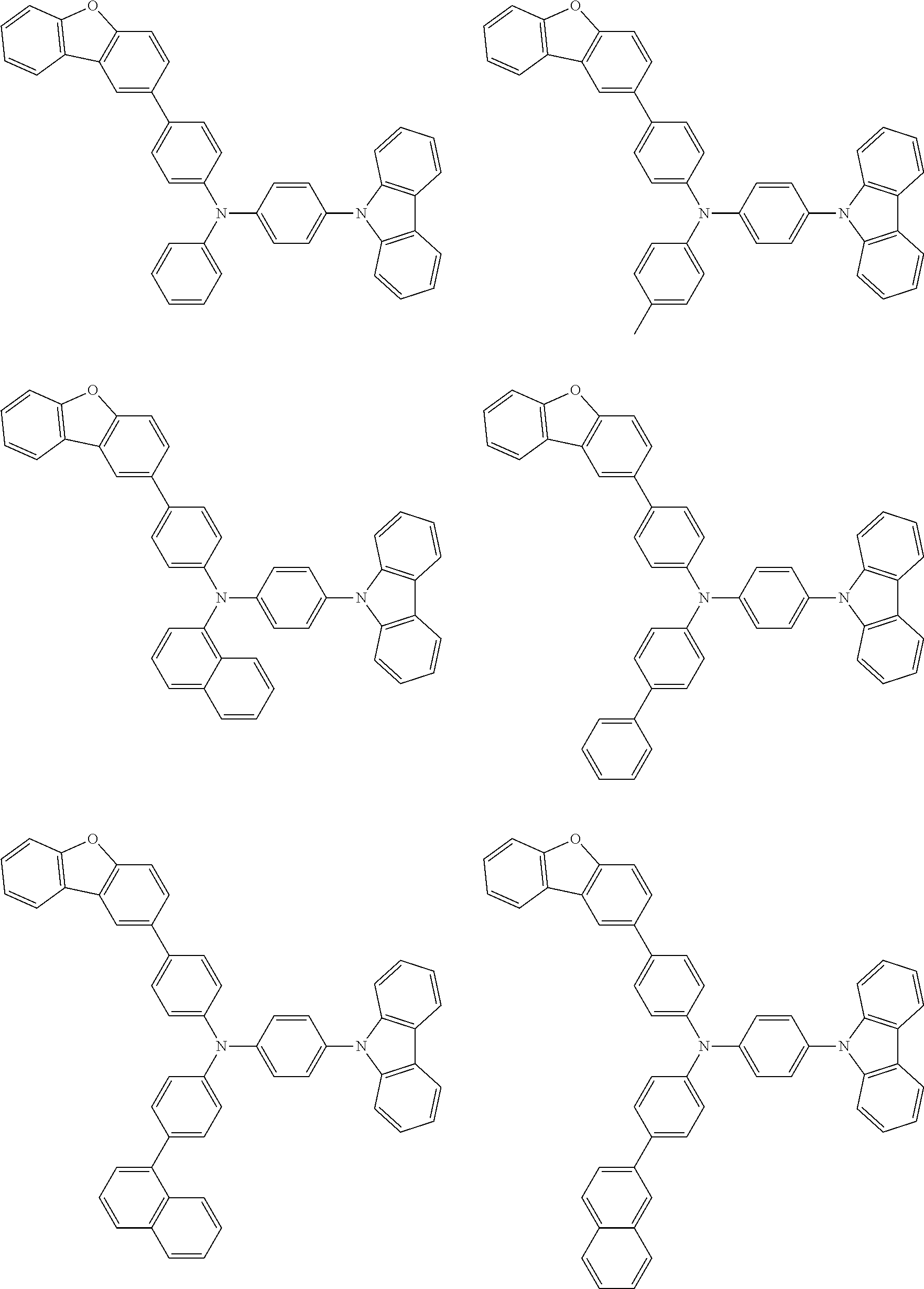


Example of Material for Hole Transporting Layer Adjacent to Light Emitting Layer (Second Hole Transporting Material);

wherein in the formulae (5) to (7),

wherein in the formula (8),

wherein in the formula (10),

wherein in the formula (10-1), Ar33 represents a substituted or unsubstituted aryl group having from 6 to 50 ring carbon atoms or a heterocyclic group having from 5 to 50 ring atoms; R81 to R88 have the same definition as above; R89 has the same definition as R81 to R88; and a represents an integer of from 1 to 7.

wherein in the formula (11),


wherein in the formulae (31) to (33),
wherein X represents a condensed ring containing a nitrogen atom or a sulfur atom; Y represents a group that is formed of a sole member or a combination of a single bond, an alkyl chain, an alkylene chain, a cycloalkyl chain, an aryl chain, a heterocyclic chain, a silyl chain, an ether chain and a thioether chain; and q represents a natural number of 2 or more.
wherein A represents a substituent having a phenanthroline skeleton or a benzoquinoline skeleton; B represents a p-valent organic group having a structure represented by the following formula (35A); and p represents a natural number of 2 or more.

wherein R4 and R5 each independently represent an alkyl group or an aryl group (including an aryl group condensed with a phenyl group); 1 and m each independently represent a natural number of from 0 to 5; and Z represents at least one group selected from the following formula (35B).

wherein R6 and R7, which may be the same as or different from each other, each are selected from a hydrogen atom, an alkyl group, a cycloalkyl group, a heterocyclic ring group, an alkenyl group, a cycloalkenyl group, an alkynyl group, an alkoxy group, an alkylthio group, an arylether group, an arylthioether group, an aryl group, a heteroaryl group, a cyano group, a carbonyl group, an ester group, a carbamoyl group, an amino group, a silyl group and a condensed ring formed with the plural adjacent groups; and Ar4 represents an aryl group or a heteroaryl group.

First Hole Transporting Material (H1)

Second Hole Transporting Material (X1)

Host Material (B)

Dopant Ir(ppy)3

Electron Transporting Material (C)


First Hole Transporting Material (H3)

First Hole Transporting Material (H4)

First Hole Transporting Material (H5)

First Hole Transporting Material (H6)

First Hole Transporting Material (H7)

First Hole Transporting Material (H8)


Comparative Compound 2

Comparative Compound 3

Comparative Compound 4
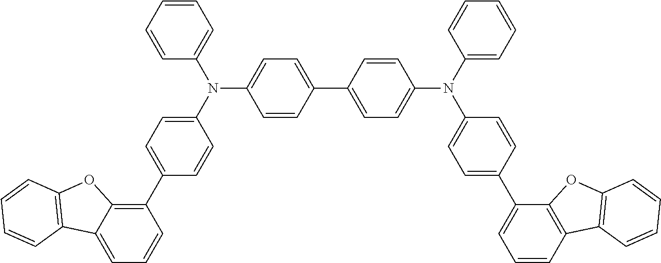

Second Hole Transporting Material (Y2)

Second Hole Transporting Material (Y3)

Second Hole Transporting Material (Y4)

Second Hole Transporting Material (Y5)

Second Hole Transporting Material (Y6)

Second Hole Transporting Material (Y7)

Second Hole Transporting Material (Y8)

Second Hole Transporting Material (Y9)

Dopant Ir(bzq)3

| TABLE 1 | ||
| Light emission capability | ||
| Light emitting | Light | ||||||||
| First hole | Second hole | material | emitting | Driving | 80% life | Light | |||
| Acceptor | transporting | transporting | (host material/ | efficiency | voltage | time *1 | emission | ||
| material | material | material | dopant) | (cd/A) | (V) | (hr) | color | ||
| Example | 1 | A | H1 | X1 | B/Ir(ppy)3 | 66.2 | 3.2 | 200 | green |
| 2 | A | H2 | X1 | B/Ir(ppy)3 | 68.2 | 3.3 | 190 | green | |
| 3 | A | H3 | X1 | B/Ir(ppy)3 | 68.1 | 3.3 | 190 | green | |
| 4 | A | H4 | X1 | B/Ir(ppy)3 | 60.5 | 3.3 | 210 | green | |
| 5 | A | H5 | X1 | B/Ir(ppy)3 | 64.1 | 3.1 | 150 | green | |
| 6 | A | H6 | X1 | B/Ir(ppy)3 | 60.5 | 3.3 | 170 | green | |
| 7 | A | H7 | X1 | B/Ir(ppy)3 | 63.2 | 3.2 | 150 | green | |
| 8 | A | H8 | X1 | B/Ir(ppy)3 | 65.3 | 3.3 | 190 | green | |
| Comparative | 1 | A | Comparative | X1 | B/Ir(ppy)3 | 59.7 | 3.3 | 120 | green |
| Example | compound 1 | ||||||||
| 2 | A | Comparative | X1 | B/Ir(ppy)3 | 60.1 | 3.4 | 40 | green | |
| compound 2 | |||||||||
| 3 | A | Comparative | X1 | B/Ir(ppy)3 | 54.8 | 3.2 | 100 | green | |
| compound 3 | |||||||||
| 4 | A | Comparative | X1 | B/Ir(ppy)3 | 56.2 | 3.6 | 70 | green | |
| compound 4 |
| 5 | A | H1 (only one hole transporting layer) | B/Ir(ppy)3 | 40.2 | 3.4 | 40 | green | ||
| *1: time of decreasing luminance to 80% | |||||||||
| TABLE 2 | ||
| Light emission capability | ||
| Light emitting | Light | ||||||||
| First hole | Second hole | material | emitting | Driving | 80% life | Light | |||
| Acceptor | transporting | transporting | (host material/ | efficiency | voltage | time *1 | emission | ||
| material | material | material | dopant) | (cd/A) | (V) | (hr) | color | ||
| Example | 9 | A | H8 | Y1 | B/Ir(bzq)3 | 57.4 | 3.7 | 580 | yellow |
| 10 | A | H8 | Y2 | B/Ir(bzq)3 | 57.1 | 3.7 | 580 | yellow | |
| 11 | A | H8 | Y3 | B/Ir(bzq)3 | 57.3 | 3.6 | 580 | yellow | |
| 12 | A | H8 | Y4 | B/Ir(bzq)3 | 62.5 | 3.6 | 610 | yellow | |
| 13 | A | H8 | Y5 | B/Ir(bzq)3 | 58.2 | 3.7 | 600 | yellow | |
| 14 | A | H8 | Y6 | B/Ir(bzq)3 | 58.6 | 3.8 | 600 | yellow | |
| 15 | A | H8 | Y7 | B/Ir(bzq)3 | 56.5 | 3.7 | 600 | yellow | |
| 16 | A | H8 | Y8 | B/Ir(bzq)3 | 55.4 | 3.7 | 600 | yellow | |
| 17 | A | H8 | Y9 | B/Ir(bzq)3 | 61.2 | 3.6 | 600 | yellow | |
| Comparative | 6 | A | Comparative | Y1 | B/Ir(bzq)3 | 51.8 | 3.8 | 350 | yellow |
| Example | compound 1 | ||||||||
| 7 | A | Comparative | Y1 | B/Ir(bzq)3 | 52.1 | 3.9 | 50 | yellow | |
| compound 2 | |||||||||
| 8 | A | Comparative | Y1 | B/Ir(bzq)3 | 47.5 | 3.7 | 130 | yellow | |
| compound 3 | |||||||||
| 9 | A | Comparative | Y1 | B/Ir(bzq)3 | 48.7 | 4.1 | 120 | yellow | |
| compound 4 | |||||||||
| *1: time of decreasing luminance to 80% | |||||||||

Second Hole Transporting Material (Y1)

Host Material (B2)

Dopant (BD)

Electron Transporting Material (C2)

Electron Transporting Material (C)

| TABLE 3 | ||
| Light emission capability | ||
| Light emitting | Light | ||||||||
| First hole | Second hole | material | emitting | Driving | 80% life | Light | |||
| Acceptor | transporting | transporting | (host material/ | efficiency | voltage | time *1 | emission | ||
| material | material | material | dopant) | (cd/A) | (V) | (hr) | color | ||
| Example | 18 | A | H8 | Y1 | B2/BD | 8.5 | 4.3 | 900 | blue |
| 19 | A | H8 | Y2 | B2/BD | 8.6 | 4.3 | 700 | blue | |
| 20 | A | H8 | Y3 | B2/BD | 8.8 | 4.3 | 700 | blue | |
| Comparative | 10 | A | Comparative | Y1 | B2/BD | 7.6 | 4 | 440 | blue |
| Example | compound 1 | ||||||||
| 11 | A | Comparative | Y1 | B2/BD | 6.7 | 4.1 | 50 | blue | |
| compound 2 | |||||||||
| 12 | A | Comparative | Y1 | B2/BD | 6.5 | 3.9 | 300 | blue | |
| compound 3 | |||||||||
| 13 | A | Comparative | Y1 | B2/BD | 7.3 | 4.3 | 310 | blue | |
| compound 4 | |||||||||
| *1: time of decreasing luminance to 80% | |||||||||
Claims (34)


Priority Applications (1)
| Application Number | Priority Date | Filing Date | Title |
|---|---|---|---|
| US13/767,417 US9966539B2 (en) | 2012-08-31 | 2013-02-14 | Organic electroluminescence device |
Applications Claiming Priority (2)
| Application Number | Priority Date | Filing Date | Title |
|---|---|---|---|
| US201261695498P | 2012-08-31 | 2012-08-31 | |
| US13/767,417 US9966539B2 (en) | 2012-08-31 | 2013-02-14 | Organic electroluminescence device |
Publications (2)
| Publication Number | Publication Date |
|---|---|
| US20140061602A1 US20140061602A1 (en) | 2014-03-06 |
| US9966539B2 true US9966539B2 (en) | 2018-05-08 |
Family
ID=50186179
Family Applications (1)
| Application Number | Title | Priority Date | Filing Date |
|---|---|---|---|
| US13/767,417 Active 2034-11-08 US9966539B2 (en) | 2012-08-31 | 2013-02-14 | Organic electroluminescence device |
Country Status (1)
| Country | Link |
|---|---|
| US (1) | US9966539B2 (en) |
Cited By (1)
| Publication number | Priority date | Publication date | Assignee | Title |
|---|---|---|---|---|
| US11380851B2 (en) * | 2017-09-01 | 2022-07-05 | Lg Chem, Ltd. | Compound and organic light emitting device comprising the same |
Families Citing this family (10)
| Publication number | Priority date | Publication date | Assignee | Title |
|---|---|---|---|---|
| CN102596907B (en) * | 2009-11-16 | 2014-12-17 | 出光兴产株式会社 | aromatic amine derivative and organic electroluminescent element using same |
| US10056558B2 (en) | 2011-11-25 | 2018-08-21 | Idemitsu Kosan Co., Ltd. | Aromatic amine derivative, material for organic electroluminescent element, and organic electroluminescent element |
| US9748492B2 (en) | 2012-11-02 | 2017-08-29 | Idemitsu Kosan Co., Ltd. | Organic electroluminescent device |
| KR101502316B1 (en) * | 2014-04-18 | 2015-03-13 | 롬엔드하스전자재료코리아유한회사 | Multi-component host material and an organic electroluminescence device comprising the same |
| KR102491209B1 (en) * | 2014-04-29 | 2023-01-26 | 롬엔드하스전자재료코리아유한회사 | Multi-Component Host Material and Organic Electroluminescent Device Comprising the Same |
| WO2015167259A1 (en) * | 2014-04-29 | 2015-11-05 | Rohm And Haas Electronic Materials Korea Ltd. | Multi-component host material and organic electroluminescent device comprising the same |
| JP2016086147A (en) * | 2014-10-29 | 2016-05-19 | 保土谷化学工業株式会社 | Organic electroluminescence device |
| US10600966B2 (en) * | 2015-02-27 | 2020-03-24 | Universal Display Corporation | Organic electroluminescent materials and devices |
| JP2020093979A (en) | 2017-03-08 | 2020-06-18 | 出光興産株式会社 | Compound, material for organic electroluminescence device, organic electroluminescence device, and electronic device |
| KR102827516B1 (en) * | 2019-04-17 | 2025-07-01 | 엘지디스플레이 주식회사 | Organic light emitting device |
Citations (26)
| Publication number | Priority date | Publication date | Assignee | Title |
|---|---|---|---|---|
| JPH11162649A (en) | 1997-11-28 | 1999-06-18 | Mitsui Chem Inc | Organic electroluminescent element |
| JPH11224779A (en) | 1998-02-04 | 1999-08-17 | Mitsui Chem Inc | Organic electroluminescent element |
| WO2001049806A1 (en) | 1999-12-31 | 2001-07-12 | Lg Chemical Co., Ltd | Electronic device comprising organic compound having p-type semiconducting characteristics |
| US20040241491A1 (en) * | 2003-05-28 | 2004-12-02 | Eastman Kodak Company | White light-emitting device structures |
| WO2005079118A1 (en) | 2004-02-13 | 2005-08-25 | Idemitsu Kosan Co., Ltd. | Organic electroluminescent device |
| JP3792029B2 (en) | 1997-11-25 | 2006-06-28 | 三井化学株式会社 | Organic electroluminescence device |
| JP3813003B2 (en) | 1997-09-04 | 2006-08-23 | 三井化学株式会社 | Organic electroluminescence device |
| US20060232198A1 (en) | 2005-04-18 | 2006-10-19 | Idemitsu Kosan Co., Ltd. | Aromatic triamine compound and organic electroluminescence device using the same |
| US20070082226A1 (en) | 2005-10-07 | 2007-04-12 | Au Optronics Corp. | Organic light emitting diode and display device employing the same |
| JP2008071993A (en) * | 2006-09-15 | 2008-03-27 | Toray Ind Inc | Light-emitting element |
| WO2008114921A1 (en) | 2007-03-21 | 2008-09-25 | Jiyoungsa Co., Ltd | Steering wheel for automobile and method for fabricating the same |
| US20080265216A1 (en) | 2007-04-30 | 2008-10-30 | Novaled Ag | Oxocarbon-, pseudooxocarbon- and radialene compounds and their use |
| WO2009041635A1 (en) | 2007-09-28 | 2009-04-02 | Idemitsu Kosan Co., Ltd. | Organic el device |
| US20090315022A1 (en) * | 2007-11-30 | 2009-12-24 | Idemitsu Kosan Co., Ltd. | Azaindenofluorenedione derivative, material for organic electroluminescence device and organic electroluminescence device |
| US20100102709A1 (en) | 2008-04-29 | 2010-04-29 | Olaf Zeika | Radialene compounds and their use |
| US20100187518A1 (en) * | 2007-07-12 | 2010-07-29 | Sumitomo Chemical Company, Limited | Method of producing organic light emitting device |
| US20100219400A1 (en) | 2009-02-27 | 2010-09-02 | Idemitsu Kosan Co., Ltd. | Organic electroluminescent device |
| WO2010114017A1 (en) | 2009-04-01 | 2010-10-07 | 出光興産株式会社 | Organic electroluminescent element |
| WO2010134352A1 (en) | 2009-05-22 | 2010-11-25 | 出光興産株式会社 | Organic electroluminescent element |
| WO2010134350A1 (en) | 2009-05-22 | 2010-11-25 | 出光興産株式会社 | Organic electroluminescent element |
| JP2010270103A (en) | 2009-04-23 | 2010-12-02 | Canon Inc | Novel organic compound, light emitting device and image display device |
| WO2011024451A1 (en) | 2009-08-28 | 2011-03-03 | 保土谷化学工業株式会社 | Organic electroluminescent element and compound having carbazole ring structure |
| WO2011090149A1 (en) | 2010-01-21 | 2011-07-28 | 出光興産株式会社 | Aromatic amine derivative, and organic electroluminescent element comprising same |
| US20110297924A1 (en) * | 2009-02-18 | 2011-12-08 | Idemitsu Kosan Co., Ltd. | Aromatic amine derivative and organic electroluminescent element |
| US20110315967A1 (en) * | 2010-06-24 | 2011-12-29 | Basf Se | Organic field effect transistor with improved current on/off ratio and controllable threshold shift |
| WO2012011756A1 (en) * | 2010-07-21 | 2012-01-26 | Rohm And Haas Electronic Materials Korea Ltd. | Novel organic electroluminescent compounds and organic electroluminescent devices including the same |
-
2013
- 2013-02-14 US US13/767,417 patent/US9966539B2/en active Active
Patent Citations (36)
| Publication number | Priority date | Publication date | Assignee | Title |
|---|---|---|---|---|
| JP3813003B2 (en) | 1997-09-04 | 2006-08-23 | 三井化学株式会社 | Organic electroluminescence device |
| JP3792029B2 (en) | 1997-11-25 | 2006-06-28 | 三井化学株式会社 | Organic electroluminescence device |
| JPH11162649A (en) | 1997-11-28 | 1999-06-18 | Mitsui Chem Inc | Organic electroluminescent element |
| JP3801330B2 (en) | 1997-11-28 | 2006-07-26 | 三井化学株式会社 | Organic electroluminescence device |
| JPH11224779A (en) | 1998-02-04 | 1999-08-17 | Mitsui Chem Inc | Organic electroluminescent element |
| JP3835917B2 (en) | 1998-02-04 | 2006-10-18 | 三井化学株式会社 | Organic electroluminescence device |
| WO2001049806A1 (en) | 1999-12-31 | 2001-07-12 | Lg Chemical Co., Ltd | Electronic device comprising organic compound having p-type semiconducting characteristics |
| JP2003519432A (en) | 1999-12-31 | 2003-06-17 | エルジー・ケミカル・カンパニー・リミテッド | Electronic device comprising an organic compound having p-type semiconductor properties |
| US20040241491A1 (en) * | 2003-05-28 | 2004-12-02 | Eastman Kodak Company | White light-emitting device structures |
| WO2005079118A1 (en) | 2004-02-13 | 2005-08-25 | Idemitsu Kosan Co., Ltd. | Organic electroluminescent device |
| US20060232198A1 (en) | 2005-04-18 | 2006-10-19 | Idemitsu Kosan Co., Ltd. | Aromatic triamine compound and organic electroluminescence device using the same |
| US20090115320A1 (en) | 2005-04-18 | 2009-05-07 | Idemitsu Kosan Co., Ltd. | Aromatic triamine compound and organic electtroluminescence device using the same |
| US20070082226A1 (en) | 2005-10-07 | 2007-04-12 | Au Optronics Corp. | Organic light emitting diode and display device employing the same |
| JP2008071993A (en) * | 2006-09-15 | 2008-03-27 | Toray Ind Inc | Light-emitting element |
| WO2008114921A1 (en) | 2007-03-21 | 2008-09-25 | Jiyoungsa Co., Ltd | Steering wheel for automobile and method for fabricating the same |
| US20080265216A1 (en) | 2007-04-30 | 2008-10-30 | Novaled Ag | Oxocarbon-, pseudooxocarbon- and radialene compounds and their use |
| JP2009010338A (en) | 2007-04-30 | 2009-01-15 | Novaled Ag | Oxocarbon compounds, pseudo-oxocarbon compounds, and radialene compounds, and methods for using them |
| US20110309309A1 (en) | 2007-04-30 | 2011-12-22 | Novaled Ag | Oxocarbon-, Pseudooxocarbon- and Radialene Compounds and Their Use |
| US20100187518A1 (en) * | 2007-07-12 | 2010-07-29 | Sumitomo Chemical Company, Limited | Method of producing organic light emitting device |
| WO2009041635A1 (en) | 2007-09-28 | 2009-04-02 | Idemitsu Kosan Co., Ltd. | Organic el device |
| US20100219404A1 (en) * | 2007-09-28 | 2010-09-02 | Idemitsu Kosan Co., Ltd. | Organic el device |
| US20090315022A1 (en) * | 2007-11-30 | 2009-12-24 | Idemitsu Kosan Co., Ltd. | Azaindenofluorenedione derivative, material for organic electroluminescence device and organic electroluminescence device |
| US20100102709A1 (en) | 2008-04-29 | 2010-04-29 | Olaf Zeika | Radialene compounds and their use |
| US20110297924A1 (en) * | 2009-02-18 | 2011-12-08 | Idemitsu Kosan Co., Ltd. | Aromatic amine derivative and organic electroluminescent element |
| WO2010098458A1 (en) | 2009-02-27 | 2010-09-02 | 出光興産株式会社 | Organic electroluminescent element |
| US20100219400A1 (en) | 2009-02-27 | 2010-09-02 | Idemitsu Kosan Co., Ltd. | Organic electroluminescent device |
| WO2010114017A1 (en) | 2009-04-01 | 2010-10-07 | 出光興産株式会社 | Organic electroluminescent element |
| US20120074395A1 (en) | 2009-04-01 | 2012-03-29 | Idemitsu Kosan Co., Ltd. | Organic electroluminescent element |
| JP2010270103A (en) | 2009-04-23 | 2010-12-02 | Canon Inc | Novel organic compound, light emitting device and image display device |
| US20120025183A1 (en) | 2009-04-23 | 2012-02-02 | Canon Kabushiki Kaisha | Novel organic compound, light-emitting device, and image display apparatus |
| WO2010134352A1 (en) | 2009-05-22 | 2010-11-25 | 出光興産株式会社 | Organic electroluminescent element |
| WO2010134350A1 (en) | 2009-05-22 | 2010-11-25 | 出光興産株式会社 | Organic electroluminescent element |
| WO2011024451A1 (en) | 2009-08-28 | 2011-03-03 | 保土谷化学工業株式会社 | Organic electroluminescent element and compound having carbazole ring structure |
| WO2011090149A1 (en) | 2010-01-21 | 2011-07-28 | 出光興産株式会社 | Aromatic amine derivative, and organic electroluminescent element comprising same |
| US20110315967A1 (en) * | 2010-06-24 | 2011-12-29 | Basf Se | Organic field effect transistor with improved current on/off ratio and controllable threshold shift |
| WO2012011756A1 (en) * | 2010-07-21 | 2012-01-26 | Rohm And Haas Electronic Materials Korea Ltd. | Novel organic electroluminescent compounds and organic electroluminescent devices including the same |
Non-Patent Citations (2)
| Title |
|---|
| C.W. Tang, et al., "Organic Electroluminescent Diodes", Appl. Phys. Lett. 51, (12), Sep. 21, 1987, American Institute of Physics, 3 pages. |
| International Search Report and Written Opinion dated Apr. 9, 2013 in PCT/JP2013/052842. |
Cited By (1)
| Publication number | Priority date | Publication date | Assignee | Title |
|---|---|---|---|---|
| US11380851B2 (en) * | 2017-09-01 | 2022-07-05 | Lg Chem, Ltd. | Compound and organic light emitting device comprising the same |
Also Published As
| Publication number | Publication date |
|---|---|
| US20140061602A1 (en) | 2014-03-06 |
Similar Documents
| Publication | Publication Date | Title |
|---|---|---|
| US9871203B2 (en) | Aromatic amine derivative, organic electroluminescent element and electronic device | |
| US9966539B2 (en) | Organic electroluminescence device | |
| US10230057B2 (en) | Biscarbazole derivatives and organic electroluminescence device employing the same | |
| US8987715B2 (en) | Organic electroluminescence element | |
| US10270040B2 (en) | Oxygen-containing fused ring amine compound, sulfur-containing fused ring amine compound and organic electroluminescence device | |
| US10388885B2 (en) | Organic electroluminescent device | |
| US9502667B2 (en) | Organic electroluminescence | |
| US8389131B2 (en) | Material for use in phosphorescent device and organic electroluminescent device using same | |
| US9966541B2 (en) | Biscarbazole derivative host materials and green emitter for OLED emissive region | |
| US20130092913A1 (en) | Organic electroluminescent element | |
| US9954178B2 (en) | Aromatic amine derivative and organic electroluminescent element | |
| US10622569B2 (en) | Compound, organic electroluminescent element, and electronic device | |
| US20120181518A1 (en) | Organic electroluminescence device | |
| US20120074395A1 (en) | Organic electroluminescent element | |
| US10205099B2 (en) | Condensed fluoranthene compound, organic electroluminescence element material including same, organic electroluminescence element using same, and electronic device | |
| US20160322587A1 (en) | Condensed fluoranthene compound, material for organic electroluminescent element using this compound, organic electroluminescent element using this material, and electronic device | |
| WO2013118812A1 (en) | Organic electroluminescent element | |
| US20120091438A1 (en) | Organic electroluminescent element | |
| US20120126217A1 (en) | Fluorene-containing aromatic compound, material for organic electroluminescent element, and organic electroluminescent element using same | |
| US20100295027A1 (en) | Organic electroluminescence device | |
| US11374178B2 (en) | Organic electroluminescent element | |
| US20140167003A1 (en) | Organic electroluminescence device | |
| US20150364692A1 (en) | Compound, material for organic electroluminescent elements, organic electroluminescent element, and electronic device | |
| US12484443B2 (en) | Organic electroluminescent element |
Legal Events
| Date | Code | Title | Description |
|---|---|---|---|
| AS | Assignment |
Owner name: IDEMITSU KOSAN CO., LTD, JAPAN Free format text: ASSIGNMENT OF ASSIGNORS INTEREST;ASSIGNORS:KATO, TOMOKI;SADO, TAKAYASU;FUJIYAMA, TAKAHIRO;SIGNING DATES FROM 20130220 TO 20130308;REEL/FRAME:030425/0571 Owner name: MITSUI CHEMICALS, INC., JAPAN Free format text: ASSIGNMENT OF ASSIGNORS INTEREST;ASSIGNORS:KATO, TOMOKI;SADO, TAKAYASU;FUJIYAMA, TAKAHIRO;SIGNING DATES FROM 20130220 TO 20130308;REEL/FRAME:030425/0571 |
|
| AS | Assignment |
Owner name: IDEMITSU KOSAN CO., LTD., JAPAN Free format text: ASSIGNMENT OF ASSIGNORS INTEREST;ASSIGNOR:MITSUI CHEMICALS, INC.;REEL/FRAME:037638/0595 Effective date: 20160128 |
|
| STCF | Information on status: patent grant |
Free format text: PATENTED CASE |
|
| CC | Certificate of correction | ||
| MAFP | Maintenance fee payment |
Free format text: PAYMENT OF MAINTENANCE FEE, 4TH YEAR, LARGE ENTITY (ORIGINAL EVENT CODE: M1551); ENTITY STATUS OF PATENT OWNER: LARGE ENTITY Year of fee payment: 4 |
|
| MAFP | Maintenance fee payment |
Free format text: PAYMENT OF MAINTENANCE FEE, 8TH YEAR, LARGE ENTITY (ORIGINAL EVENT CODE: M1552); ENTITY STATUS OF PATENT OWNER: LARGE ENTITY Year of fee payment: 8 |