WO2010134350A1 - Organic electroluminescent element - Google Patents
Organic electroluminescent element Download PDFInfo
- Publication number
- WO2010134350A1 WO2010134350A1 PCT/JP2010/003431 JP2010003431W WO2010134350A1 WO 2010134350 A1 WO2010134350 A1 WO 2010134350A1 JP 2010003431 W JP2010003431 W JP 2010003431W WO 2010134350 A1 WO2010134350 A1 WO 2010134350A1
- Authority
- WO
- WIPO (PCT)
- Prior art keywords
- group
- light emitting
- layer
- emitting layer
- barrier layer
- Prior art date
Links
- 230000004888 barrier function Effects 0.000 claims abstract description 112
- 239000002019 doping agent Substances 0.000 claims abstract description 99
- -1 hydrocarbon aromatic compound Chemical class 0.000 claims description 322
- 238000005401 electroluminescence Methods 0.000 claims description 74
- 239000000463 material Substances 0.000 claims description 54
- 150000001875 compounds Chemical class 0.000 claims description 37
- 238000002347 injection Methods 0.000 claims description 36
- 239000007924 injection Substances 0.000 claims description 36
- 230000005525 hole transport Effects 0.000 claims description 28
- 230000005684 electric field Effects 0.000 claims description 10
- 125000004122 cyclic group Chemical group 0.000 claims description 8
- ZOXJGFHDIHLPTG-UHFFFAOYSA-N Boron Chemical compound [B] ZOXJGFHDIHLPTG-UHFFFAOYSA-N 0.000 claims description 7
- 229910052796 boron Inorganic materials 0.000 claims description 7
- 239000004215 Carbon black (E152) Substances 0.000 claims description 6
- 229930195733 hydrocarbon Natural products 0.000 claims description 6
- 125000003914 fluoranthenyl group Chemical class C1(=CC=C2C=CC=C3C4=CC=CC=C4C1=C23)* 0.000 claims description 4
- 239000011368 organic material Substances 0.000 claims description 4
- 230000001747 exhibiting effect Effects 0.000 claims description 3
- 239000010410 layer Substances 0.000 description 343
- 125000004432 carbon atom Chemical group C* 0.000 description 108
- 125000003118 aryl group Chemical group 0.000 description 58
- 125000000217 alkyl group Chemical group 0.000 description 31
- 150000001454 anthracenes Chemical class 0.000 description 25
- 230000000052 comparative effect Effects 0.000 description 25
- 125000006413 ring segment Chemical group 0.000 description 25
- 125000001424 substituent group Chemical group 0.000 description 23
- 125000000753 cycloalkyl group Chemical group 0.000 description 20
- 238000000034 method Methods 0.000 description 19
- 230000001052 transient effect Effects 0.000 description 14
- 125000002676 chrysenyl group Chemical group C1(=CC=CC=2C3=CC=C4C=CC=CC4=C3C=CC12)* 0.000 description 13
- NAWXUBYGYWOOIX-SFHVURJKSA-N (2s)-2-[[4-[2-(2,4-diaminoquinazolin-6-yl)ethyl]benzoyl]amino]-4-methylidenepentanedioic acid Chemical compound C1=CC2=NC(N)=NC(N)=C2C=C1CCC1=CC=C(C(=O)N[C@@H](CC(=C)C(O)=O)C(O)=O)C=C1 NAWXUBYGYWOOIX-SFHVURJKSA-N 0.000 description 12
- 238000011156 evaluation Methods 0.000 description 12
- 125000004435 hydrogen atom Chemical group [H]* 0.000 description 12
- 229910052751 metal Inorganic materials 0.000 description 12
- 239000002184 metal Substances 0.000 description 12
- 238000005215 recombination Methods 0.000 description 11
- 230000006798 recombination Effects 0.000 description 11
- 239000000758 substrate Substances 0.000 description 11
- 150000002219 fluoranthenes Chemical class 0.000 description 10
- 125000005843 halogen group Chemical group 0.000 description 10
- 125000001637 1-naphthyl group Chemical group [H]C1=C([H])C([H])=C2C(*)=C([H])C([H])=C([H])C2=C1[H] 0.000 description 9
- 125000001622 2-naphthyl group Chemical group [H]C1=C([H])C([H])=C2C([H])=C(*)C([H])=C([H])C2=C1[H] 0.000 description 9
- 229910052783 alkali metal Inorganic materials 0.000 description 9
- 150000001340 alkali metals Chemical class 0.000 description 9
- GVEPBJHOBDJJJI-UHFFFAOYSA-N fluoranthene Chemical compound C1=CC(C2=CC=CC=C22)=C3C2=CC=CC3=C1 GVEPBJHOBDJJJI-UHFFFAOYSA-N 0.000 description 9
- 229910052705 radium Inorganic materials 0.000 description 9
- 125000004093 cyano group Chemical group *C#N 0.000 description 8
- 230000000694 effects Effects 0.000 description 8
- 125000001072 heteroaryl group Chemical group 0.000 description 8
- 238000005259 measurement Methods 0.000 description 8
- 125000001997 phenyl group Chemical group [H]C1=C([H])C([H])=C(*)C([H])=C1[H] 0.000 description 8
- 125000003710 aryl alkyl group Chemical group 0.000 description 7
- 238000010549 co-Evaporation Methods 0.000 description 7
- 238000010586 diagram Methods 0.000 description 7
- 125000000623 heterocyclic group Chemical group 0.000 description 7
- 238000004768 lowest unoccupied molecular orbital Methods 0.000 description 7
- 229910052701 rubidium Inorganic materials 0.000 description 7
- 150000004982 aromatic amines Chemical class 0.000 description 6
- 125000000732 arylene group Chemical group 0.000 description 6
- 229910052799 carbon Inorganic materials 0.000 description 6
- 230000005281 excited state Effects 0.000 description 6
- 230000005283 ground state Effects 0.000 description 6
- YNPNZTXNASCQKK-UHFFFAOYSA-N phenanthrene Chemical group C1=CC=C2C3=CC=CC=C3C=CC2=C1 YNPNZTXNASCQKK-UHFFFAOYSA-N 0.000 description 6
- 125000003545 alkoxy group Chemical group 0.000 description 5
- 125000001769 aryl amino group Chemical group 0.000 description 5
- 150000004696 coordination complex Chemical class 0.000 description 5
- 125000003983 fluorenyl group Chemical group C1(=CC=CC=2C3=CC=CC=C3CC12)* 0.000 description 5
- 125000003808 silyl group Chemical group [H][Si]([H])([H])[*] 0.000 description 5
- 238000012546 transfer Methods 0.000 description 5
- STTGYIUESPWXOW-UHFFFAOYSA-N 2,9-dimethyl-4,7-diphenyl-1,10-phenanthroline Chemical compound C=12C=CC3=C(C=4C=CC=CC=4)C=C(C)N=C3C2=NC(C)=CC=1C1=CC=CC=C1 STTGYIUESPWXOW-UHFFFAOYSA-N 0.000 description 4
- OKTJSMMVPCPJKN-UHFFFAOYSA-N Carbon Chemical group [C] OKTJSMMVPCPJKN-UHFFFAOYSA-N 0.000 description 4
- 229910052784 alkaline earth metal Inorganic materials 0.000 description 4
- 150000001342 alkaline earth metals Chemical class 0.000 description 4
- 125000004453 alkoxycarbonyl group Chemical group 0.000 description 4
- 125000004104 aryloxy group Chemical group 0.000 description 4
- UHOVQNZJYSORNB-UHFFFAOYSA-N benzene Substances C1=CC=CC=C1 UHOVQNZJYSORNB-UHFFFAOYSA-N 0.000 description 4
- JZOIZKBKSZMVRV-UHFFFAOYSA-N benzo(a)triphenylene Chemical group C1=CC=CC2=C3C4=CC=CC=C4C=CC3=C(C=CC=C3)C3=C21 JZOIZKBKSZMVRV-UHFFFAOYSA-N 0.000 description 4
- 238000006243 chemical reaction Methods 0.000 description 4
- WDECIBYCCFPHNR-UHFFFAOYSA-N chrysene Chemical compound C1=CC=CC2=CC=C3C4=CC=CC=C4C=CC3=C21 WDECIBYCCFPHNR-UHFFFAOYSA-N 0.000 description 4
- 238000009792 diffusion process Methods 0.000 description 4
- 230000006870 function Effects 0.000 description 4
- 230000004927 fusion Effects 0.000 description 4
- 125000005549 heteroarylene group Chemical group 0.000 description 4
- 150000002790 naphthalenes Chemical group 0.000 description 4
- 125000001624 naphthyl group Chemical group 0.000 description 4
- 230000003647 oxidation Effects 0.000 description 4
- 238000007254 oxidation reaction Methods 0.000 description 4
- 150000003220 pyrenes Chemical class 0.000 description 4
- 125000004665 trialkylsilyl group Chemical group 0.000 description 4
- 125000005106 triarylsilyl group Chemical group 0.000 description 4
- SLGBZMMZGDRARJ-UHFFFAOYSA-N triphenylene Chemical group C1=CC=C2C3=CC=CC=C3C3=CC=CC=C3C2=C1 SLGBZMMZGDRARJ-UHFFFAOYSA-N 0.000 description 4
- 125000005580 triphenylene group Chemical group 0.000 description 4
- KFZMGEQAYNKOFK-UHFFFAOYSA-N Isopropanol Chemical compound CC(C)O KFZMGEQAYNKOFK-UHFFFAOYSA-N 0.000 description 3
- UFWIBTONFRDIAS-UHFFFAOYSA-N Naphthalene Chemical compound C1=CC=CC2=CC=CC=C21 UFWIBTONFRDIAS-UHFFFAOYSA-N 0.000 description 3
- YXFVVABEGXRONW-UHFFFAOYSA-N Toluene Chemical compound CC1=CC=CC=C1 YXFVVABEGXRONW-UHFFFAOYSA-N 0.000 description 3
- MWPLVEDNUUSJAV-UHFFFAOYSA-N anthracene Natural products C1=CC=CC2=CC3=CC=CC=C3C=C21 MWPLVEDNUUSJAV-UHFFFAOYSA-N 0.000 description 3
- 125000005110 aryl thio group Chemical group 0.000 description 3
- TUAHORSUHVUKBD-UHFFFAOYSA-N benzo[c]phenanthrene Chemical group C1=CC=CC2=C3C4=CC=CC=C4C=CC3=CC=C21 TUAHORSUHVUKBD-UHFFFAOYSA-N 0.000 description 3
- 230000000903 blocking effect Effects 0.000 description 3
- 150000001721 carbon Chemical group 0.000 description 3
- 125000003178 carboxy group Chemical group [H]OC(*)=O 0.000 description 3
- 230000008859 change Effects 0.000 description 3
- 150000001846 chrysenes Chemical group 0.000 description 3
- 230000009849 deactivation Effects 0.000 description 3
- 238000010893 electron trap Methods 0.000 description 3
- 238000000295 emission spectrum Methods 0.000 description 3
- 238000005516 engineering process Methods 0.000 description 3
- 238000000605 extraction Methods 0.000 description 3
- NIHNNTQXNPWCJQ-UHFFFAOYSA-N fluorene Chemical compound C1=CC=C2CC3=CC=CC=C3C2=C1 NIHNNTQXNPWCJQ-UHFFFAOYSA-N 0.000 description 3
- 125000002887 hydroxy group Chemical group [H]O* 0.000 description 3
- 238000001566 impedance spectroscopy Methods 0.000 description 3
- 230000006872 improvement Effects 0.000 description 3
- 125000000449 nitro group Chemical group [O-][N+](*)=O 0.000 description 3
- 239000012044 organic layer Substances 0.000 description 3
- 150000002987 phenanthrenes Chemical class 0.000 description 3
- 230000008569 process Effects 0.000 description 3
- 239000011241 protective layer Substances 0.000 description 3
- 229910052761 rare earth metal Inorganic materials 0.000 description 3
- 230000004044 response Effects 0.000 description 3
- 230000003595 spectral effect Effects 0.000 description 3
- 238000001228 spectrum Methods 0.000 description 3
- 230000007704 transition Effects 0.000 description 3
- UWRZIZXBOLBCON-VOTSOKGWSA-N (e)-2-phenylethenamine Chemical compound N\C=C\C1=CC=CC=C1 UWRZIZXBOLBCON-VOTSOKGWSA-N 0.000 description 2
- DHDHJYNTEFLIHY-UHFFFAOYSA-N 4,7-diphenyl-1,10-phenanthroline Chemical compound C1=CC=CC=C1C1=CC=NC2=C1C=CC1=C(C=3C=CC=CC=3)C=CN=C21 DHDHJYNTEFLIHY-UHFFFAOYSA-N 0.000 description 2
- 229910018068 Li 2 O Inorganic materials 0.000 description 2
- JUJWROOIHBZHMG-UHFFFAOYSA-N Pyridine Chemical group C1=CC=NC=C1 JUJWROOIHBZHMG-UHFFFAOYSA-N 0.000 description 2
- XLOMVQKBTHCTTD-UHFFFAOYSA-N Zinc monoxide Chemical compound [Zn]=O XLOMVQKBTHCTTD-UHFFFAOYSA-N 0.000 description 2
- 238000000862 absorption spectrum Methods 0.000 description 2
- 150000001339 alkali metal compounds Chemical class 0.000 description 2
- 125000002078 anthracen-1-yl group Chemical group [H]C1=C([H])C([H])=C2C([H])=C3C([*])=C([H])C([H])=C([H])C3=C([H])C2=C1[H] 0.000 description 2
- 125000000748 anthracen-2-yl group Chemical group [H]C1=C([H])C([H])=C2C([H])=C3C([H])=C([*])C([H])=C([H])C3=C([H])C2=C1[H] 0.000 description 2
- 125000005577 anthracene group Chemical group 0.000 description 2
- 125000002029 aromatic hydrocarbon group Chemical group 0.000 description 2
- 125000003609 aryl vinyl group Chemical group 0.000 description 2
- 125000004429 atom Chemical group 0.000 description 2
- 150000001555 benzenes Chemical group 0.000 description 2
- FTOVXSOBNPWTSH-UHFFFAOYSA-N benzo[b]fluoranthene Chemical group C12=CC=CC=C1C1=CC3=CC=CC=C3C3=C1C2=CC=C3 FTOVXSOBNPWTSH-UHFFFAOYSA-N 0.000 description 2
- YZWGEMSQAMDWEM-UHFFFAOYSA-N benzo[c]chrysene Chemical compound C1=CC2=CC=C3C=CC=CC3=C2C2=C1C1=CC=CC=C1C=C2 YZWGEMSQAMDWEM-UHFFFAOYSA-N 0.000 description 2
- 125000000609 carbazolyl group Chemical class C1(=CC=CC=2C3=CC=CC=C3NC12)* 0.000 description 2
- 230000015556 catabolic process Effects 0.000 description 2
- 125000000113 cyclohexyl group Chemical group [H]C1([H])C([H])([H])C([H])([H])C([H])(*)C([H])([H])C1([H])[H] 0.000 description 2
- 125000001511 cyclopentyl group Chemical group [H]C1([H])C([H])([H])C([H])([H])C([H])(*)C1([H])[H] 0.000 description 2
- 230000007423 decrease Effects 0.000 description 2
- 238000001194 electroluminescence spectrum Methods 0.000 description 2
- 125000001495 ethyl group Chemical group [H]C([H])([H])C([H])([H])* 0.000 description 2
- 238000001704 evaporation Methods 0.000 description 2
- 230000008020 evaporation Effects 0.000 description 2
- 150000002220 fluorenes Chemical class 0.000 description 2
- 150000004820 halides Chemical class 0.000 description 2
- 150000002391 heterocyclic compounds Chemical class 0.000 description 2
- 238000004770 highest occupied molecular orbital Methods 0.000 description 2
- 150000002503 iridium Chemical class 0.000 description 2
- 125000000959 isobutyl group Chemical group [H]C([H])([H])C([H])(C([H])([H])[H])C([H])([H])* 0.000 description 2
- 125000001449 isopropyl group Chemical group [H]C([H])([H])C([H])(*)C([H])([H])[H] 0.000 description 2
- 238000010030 laminating Methods 0.000 description 2
- 238000004020 luminiscence type Methods 0.000 description 2
- 229910052749 magnesium Inorganic materials 0.000 description 2
- 230000007246 mechanism Effects 0.000 description 2
- 150000002736 metal compounds Chemical class 0.000 description 2
- 150000002739 metals Chemical class 0.000 description 2
- 125000002496 methyl group Chemical group [H]C([H])([H])* 0.000 description 2
- 125000004108 n-butyl group Chemical group [H]C([H])([H])C([H])([H])C([H])([H])C([H])([H])* 0.000 description 2
- 229910052757 nitrogen Inorganic materials 0.000 description 2
- 230000003287 optical effect Effects 0.000 description 2
- 150000005041 phenanthrolines Chemical class 0.000 description 2
- 238000001296 phosphorescence spectrum Methods 0.000 description 2
- 230000000704 physical effect Effects 0.000 description 2
- 150000003057 platinum Chemical class 0.000 description 2
- 125000001436 propyl group Chemical group [H]C([*])([H])C([H])([H])C([H])([H])[H] 0.000 description 2
- BBEAQIROQSPTKN-UHFFFAOYSA-N pyrene Chemical compound C1=CC=C2C=CC3=CC=CC4=CC=C1C2=C43 BBEAQIROQSPTKN-UHFFFAOYSA-N 0.000 description 2
- 125000002943 quinolinyl group Chemical group N1=C(C=CC2=CC=CC=C12)* 0.000 description 2
- 150000002910 rare earth metals Chemical class 0.000 description 2
- 230000001360 synchronised effect Effects 0.000 description 2
- 125000000999 tert-butyl group Chemical group [H]C([H])([H])C(*)(C([H])([H])[H])C([H])([H])[H] 0.000 description 2
- 238000005406 washing Methods 0.000 description 2
- YZVWKHVRBDQPMQ-UHFFFAOYSA-N 1-aminopyrene Chemical class C1=C2C(N)=CC=C(C=C3)C2=C2C3=CC=CC2=C1 YZVWKHVRBDQPMQ-UHFFFAOYSA-N 0.000 description 1
- 125000006083 1-bromoethyl group Chemical group 0.000 description 1
- 125000001478 1-chloroethyl group Chemical group [H]C([H])([H])C([H])(Cl)* 0.000 description 1
- 125000004066 1-hydroxyethyl group Chemical group [H]OC([H])([*])C([H])([H])[H] 0.000 description 1
- 125000004134 1-norbornyl group Chemical group [H]C1([H])C([H])([H])C2(*)C([H])([H])C([H])([H])C1([H])C2([H])[H] 0.000 description 1
- 125000004343 1-phenylethyl group Chemical group [H]C1=C([H])C([H])=C(C([H])=C1[H])C([H])(*)C([H])([H])[H] 0.000 description 1
- 125000001462 1-pyrrolyl group Chemical group [*]N1C([H])=C([H])C([H])=C1[H] 0.000 description 1
- 125000000022 2-aminoethyl group Chemical group [H]C([*])([H])C([H])([H])N([H])[H] 0.000 description 1
- 125000006280 2-bromobenzyl group Chemical group [H]C1=C([H])C(Br)=C(C([H])=C1[H])C([H])([H])* 0.000 description 1
- 125000005999 2-bromoethyl group Chemical group 0.000 description 1
- 125000006282 2-chlorobenzyl group Chemical group [H]C1=C([H])C(Cl)=C(C([H])=C1[H])C([H])([H])* 0.000 description 1
- 125000001340 2-chloroethyl group Chemical group [H]C([H])(Cl)C([H])([H])* 0.000 description 1
- 125000001731 2-cyanoethyl group Chemical group [H]C([H])(*)C([H])([H])C#N 0.000 description 1
- 125000002941 2-furyl group Chemical group O1C([*])=C([H])C([H])=C1[H] 0.000 description 1
- 125000006290 2-hydroxybenzyl group Chemical group [H]OC1=C(C([H])=C([H])C([H])=C1[H])C([H])([H])* 0.000 description 1
- 125000000954 2-hydroxyethyl group Chemical group [H]C([*])([H])C([H])([H])O[H] 0.000 description 1
- 125000006481 2-iodobenzyl group Chemical group [H]C1=C([H])C(I)=C(C([H])=C1[H])C([H])([H])* 0.000 description 1
- NSMJMUQZRGZMQC-UHFFFAOYSA-N 2-naphthalen-1-yl-1H-imidazo[4,5-f][1,10]phenanthroline Chemical compound C12=CC=CN=C2C2=NC=CC=C2C2=C1NC(C=1C3=CC=CC=C3C=CC=1)=N2 NSMJMUQZRGZMQC-UHFFFAOYSA-N 0.000 description 1
- 125000004135 2-norbornyl group Chemical group [H]C1([H])C([H])([H])C2([H])C([H])([H])C1([H])C([H])([H])C2([H])* 0.000 description 1
- 125000000094 2-phenylethyl group Chemical group [H]C1=C([H])C([H])=C(C([H])=C1[H])C([H])([H])C([H])([H])* 0.000 description 1
- 125000000389 2-pyrrolyl group Chemical group [H]N1C([*])=C([H])C([H])=C1[H] 0.000 description 1
- 125000000175 2-thienyl group Chemical group S1C([*])=C([H])C([H])=C1[H] 0.000 description 1
- 125000006279 3-bromobenzyl group Chemical group [H]C1=C([H])C(=C([H])C(Br)=C1[H])C([H])([H])* 0.000 description 1
- 125000003852 3-chlorobenzyl group Chemical group [H]C1=C([H])C(=C([H])C(Cl)=C1[H])C([H])([H])* 0.000 description 1
- 125000003682 3-furyl group Chemical group O1C([H])=C([*])C([H])=C1[H] 0.000 description 1
- 125000006291 3-hydroxybenzyl group Chemical group [H]OC1=C([H])C([H])=C([H])C(=C1[H])C([H])([H])* 0.000 description 1
- 125000006482 3-iodobenzyl group Chemical group [H]C1=C([H])C(=C([H])C(I)=C1[H])C([H])([H])* 0.000 description 1
- 125000001397 3-pyrrolyl group Chemical group [H]N1C([H])=C([*])C([H])=C1[H] 0.000 description 1
- 125000001541 3-thienyl group Chemical group S1C([H])=C([*])C([H])=C1[H] 0.000 description 1
- 125000006281 4-bromobenzyl group Chemical group [H]C1=C([H])C(=C([H])C([H])=C1Br)C([H])([H])* 0.000 description 1
- 125000006283 4-chlorobenzyl group Chemical group [H]C1=C([H])C(=C([H])C([H])=C1Cl)C([H])([H])* 0.000 description 1
- 125000003143 4-hydroxybenzyl group Chemical group [H]C([*])([H])C1=C([H])C([H])=C(O[H])C([H])=C1[H] 0.000 description 1
- 125000006483 4-iodobenzyl group Chemical group [H]C1=C([H])C(=C([H])C([H])=C1I)C([H])([H])* 0.000 description 1
- ZCYVEMRRCGMTRW-UHFFFAOYSA-N 7553-56-2 Chemical compound [I] ZCYVEMRRCGMTRW-UHFFFAOYSA-N 0.000 description 1
- 229910001316 Ag alloy Inorganic materials 0.000 description 1
- KHNYNFUTFKJLDD-UHFFFAOYSA-N Benzo[j]fluoranthene Chemical class C1=CC(C=2C3=CC=CC=C3C=CC=22)=C3C2=CC=CC3=C1 KHNYNFUTFKJLDD-UHFFFAOYSA-N 0.000 description 1
- BTBUEUYNUDRHOZ-UHFFFAOYSA-N Borate Chemical compound [O-]B([O-])[O-] BTBUEUYNUDRHOZ-UHFFFAOYSA-N 0.000 description 1
- WKBOTKDWSSQWDR-UHFFFAOYSA-N Bromine atom Chemical compound [Br] WKBOTKDWSSQWDR-UHFFFAOYSA-N 0.000 description 1
- APNQMOGXNCGFQJ-UHFFFAOYSA-N CC(C)(c1c2)c(cc(cc3)-[n]4c5ccccc5c5c4cccc5)c3-c1ccc2N(c1ccccc1)c1ccc2[o]c(C=CCC3)c3c2c1 Chemical compound CC(C)(c1c2)c(cc(cc3)-[n]4c5ccccc5c5c4cccc5)c3-c1ccc2N(c1ccccc1)c1ccc2[o]c(C=CCC3)c3c2c1 APNQMOGXNCGFQJ-UHFFFAOYSA-N 0.000 description 1
- GVJRXUNCDHYEED-UHFFFAOYSA-N CC1(C)c2cc(-[n]3c4ccccc4c4c3cccc4)ccc2C2C1=CC(N(c1ccc3[o]c(cccc4)c4c3c1)C1=CCC3Oc4ccccc4C3=C1)=CC2 Chemical compound CC1(C)c2cc(-[n]3c4ccccc4c4c3cccc4)ccc2C2C1=CC(N(c1ccc3[o]c(cccc4)c4c3c1)C1=CCC3Oc4ccccc4C3=C1)=CC2 GVJRXUNCDHYEED-UHFFFAOYSA-N 0.000 description 1
- 229910052684 Cerium Inorganic materials 0.000 description 1
- ZAMOUSCENKQFHK-UHFFFAOYSA-N Chlorine atom Chemical compound [Cl] ZAMOUSCENKQFHK-UHFFFAOYSA-N 0.000 description 1
- TXCDCPKCNAJMEE-UHFFFAOYSA-N Dibenzofuran Natural products C1=CC=C2C3=CC=CC=C3OC2=C1 TXCDCPKCNAJMEE-UHFFFAOYSA-N 0.000 description 1
- 229910052693 Europium Inorganic materials 0.000 description 1
- PXGOKWXKJXAPGV-UHFFFAOYSA-N Fluorine Chemical compound FF PXGOKWXKJXAPGV-UHFFFAOYSA-N 0.000 description 1
- 108010043121 Green Fluorescent Proteins Proteins 0.000 description 1
- UFHFLCQGNIYNRP-UHFFFAOYSA-N Hydrogen Chemical compound [H][H] UFHFLCQGNIYNRP-UHFFFAOYSA-N 0.000 description 1
- CBENFWSGALASAD-UHFFFAOYSA-N Ozone Chemical compound [O-][O+]=O CBENFWSGALASAD-UHFFFAOYSA-N 0.000 description 1
- 229910002668 Pd-Cu Inorganic materials 0.000 description 1
- 239000004642 Polyimide Substances 0.000 description 1
- 229910052769 Ytterbium Inorganic materials 0.000 description 1
- KPCZJLGGXRGYIE-UHFFFAOYSA-N [C]1=CC=CN=C1 Chemical group [C]1=CC=CN=C1 KPCZJLGGXRGYIE-UHFFFAOYSA-N 0.000 description 1
- 238000010521 absorption reaction Methods 0.000 description 1
- CWRYPZZKDGJXCA-UHFFFAOYSA-N acenaphthene Chemical compound C1=CC(CC2)=C3C2=CC=CC3=C1 CWRYPZZKDGJXCA-UHFFFAOYSA-N 0.000 description 1
- 125000004054 acenaphthylenyl group Chemical group C1(=CC2=CC=CC3=CC=CC1=C23)* 0.000 description 1
- HXGDTGSAIMULJN-UHFFFAOYSA-N acetnaphthylene Natural products C1=CC(C=C2)=C3C2=CC=CC3=C1 HXGDTGSAIMULJN-UHFFFAOYSA-N 0.000 description 1
- 230000009471 action Effects 0.000 description 1
- 125000003670 adamantan-2-yl group Chemical group [H]C1([H])C(C2([H])[H])([H])C([H])([H])C3([H])C([*])([H])C1([H])C([H])([H])C2([H])C3([H])[H] 0.000 description 1
- 125000003342 alkenyl group Chemical group 0.000 description 1
- 229910045601 alloy Inorganic materials 0.000 description 1
- 239000000956 alloy Substances 0.000 description 1
- 125000003277 amino group Chemical group 0.000 description 1
- 125000004202 aminomethyl group Chemical group [H]N([H])C([H])([H])* 0.000 description 1
- 238000004458 analytical method Methods 0.000 description 1
- YUENFNPLGJCNRB-UHFFFAOYSA-N anthracen-1-amine Chemical class C1=CC=C2C=C3C(N)=CC=CC3=CC2=C1 YUENFNPLGJCNRB-UHFFFAOYSA-N 0.000 description 1
- 150000001491 aromatic compounds Chemical class 0.000 description 1
- 125000006615 aromatic heterocyclic group Chemical group 0.000 description 1
- 229910052788 barium Inorganic materials 0.000 description 1
- 239000002585 base Substances 0.000 description 1
- 230000008901 benefit Effects 0.000 description 1
- 125000001797 benzyl group Chemical group [H]C1=C([H])C([H])=C(C([H])=C1[H])C([H])([H])* 0.000 description 1
- 150000001638 boron Chemical class 0.000 description 1
- GDTBXPJZTBHREO-UHFFFAOYSA-N bromine Substances BrBr GDTBXPJZTBHREO-UHFFFAOYSA-N 0.000 description 1
- 229910052794 bromium Inorganic materials 0.000 description 1
- 125000005997 bromomethyl group Chemical group 0.000 description 1
- BSDOPZVHSHOTKE-UHFFFAOYSA-N c(cc1)ccc1-c1cc(-c(cc2c3c4)ccc2[o]c3cc(c2c3)c4[o]c2ccc3-c2cccc(-c3ccccc3)c2)ccc1 Chemical compound c(cc1)ccc1-c1cc(-c(cc2c3c4)ccc2[o]c3cc(c2c3)c4[o]c2ccc3-c2cccc(-c3ccccc3)c2)ccc1 BSDOPZVHSHOTKE-UHFFFAOYSA-N 0.000 description 1
- MJOIBSPUXNMHKC-UHFFFAOYSA-N c(cc1)ccc1-c1cccc(-c2ccc3[o]c(cc(c(c4c5)c6)[o]c4ccc5-c4cccc(-c5ccccc5)c4)c6c3c2)c1 Chemical compound c(cc1)ccc1-c1cccc(-c2ccc3[o]c(cc(c(c4c5)c6)[o]c4ccc5-c4cccc(-c5ccccc5)c4)c6c3c2)c1 MJOIBSPUXNMHKC-UHFFFAOYSA-N 0.000 description 1
- 229910052792 caesium Inorganic materials 0.000 description 1
- 229910052791 calcium Inorganic materials 0.000 description 1
- 239000011203 carbon fibre reinforced carbon Substances 0.000 description 1
- BVKZGUZCCUSVTD-UHFFFAOYSA-N carbonic acid Chemical compound OC(O)=O BVKZGUZCCUSVTD-UHFFFAOYSA-N 0.000 description 1
- 150000001732 carboxylic acid derivatives Chemical class 0.000 description 1
- 239000000969 carrier Substances 0.000 description 1
- 229910052801 chlorine Inorganic materials 0.000 description 1
- 239000000460 chlorine Substances 0.000 description 1
- 125000004218 chloromethyl group Chemical group [H]C([H])(Cl)* 0.000 description 1
- OQENBJBTQPIZKA-UHFFFAOYSA-N chrysen-1-amine Chemical class C1=CC2=C3C=CC=CC3=CC=C2C2=C1C(N)=CC=C2 OQENBJBTQPIZKA-UHFFFAOYSA-N 0.000 description 1
- 239000004020 conductor Substances 0.000 description 1
- 125000006165 cyclic alkyl group Chemical group 0.000 description 1
- 238000002484 cyclic voltammetry Methods 0.000 description 1
- 125000001995 cyclobutyl group Chemical group [H]C1([H])C([H])([H])C([H])(*)C1([H])[H] 0.000 description 1
- 125000001559 cyclopropyl group Chemical group [H]C1([H])C([H])([H])C1([H])* 0.000 description 1
- 230000003247 decreasing effect Effects 0.000 description 1
- 125000005299 dibenzofluorenyl group Chemical group C1(=CC=CC2=C3C(=C4C=5C=CC=CC5CC4=C21)C=CC=C3)* 0.000 description 1
- 150000004826 dibenzofurans Chemical class 0.000 description 1
- 125000005594 diketone group Chemical group 0.000 description 1
- 238000005265 energy consumption Methods 0.000 description 1
- 238000005530 etching Methods 0.000 description 1
- 229910052731 fluorine Inorganic materials 0.000 description 1
- 239000011737 fluorine Substances 0.000 description 1
- 125000001153 fluoro group Chemical group F* 0.000 description 1
- 150000002240 furans Chemical class 0.000 description 1
- 125000001188 haloalkyl group Chemical group 0.000 description 1
- 229910052739 hydrogen Inorganic materials 0.000 description 1
- 239000001257 hydrogen Substances 0.000 description 1
- 125000004029 hydroxymethyl group Chemical group [H]OC([H])([H])* 0.000 description 1
- 230000001771 impaired effect Effects 0.000 description 1
- 238000009413 insulation Methods 0.000 description 1
- 239000011630 iodine Substances 0.000 description 1
- 229910052740 iodine Inorganic materials 0.000 description 1
- 230000001678 irradiating effect Effects 0.000 description 1
- 125000002183 isoquinolinyl group Chemical group C1(=NC=CC2=CC=CC=C12)* 0.000 description 1
- 239000003446 ligand Substances 0.000 description 1
- 229910052744 lithium Inorganic materials 0.000 description 1
- 238000001459 lithography Methods 0.000 description 1
- 125000003564 m-cyanobenzyl group Chemical group [H]C1=C([H])C(=C([H])C(C#N)=C1[H])C([H])([H])* 0.000 description 1
- 125000000040 m-tolyl group Chemical group [H]C1=C([H])C(*)=C([H])C(=C1[H])C([H])([H])[H] 0.000 description 1
- 230000004048 modification Effects 0.000 description 1
- 238000012986 modification Methods 0.000 description 1
- 125000003136 n-heptyl group Chemical group [H]C([H])([H])C([H])([H])C([H])([H])C([H])([H])C([H])([H])C([H])([H])C([H])([H])* 0.000 description 1
- 125000001280 n-hexyl group Chemical group C(CCCCC)* 0.000 description 1
- 125000000740 n-pentyl group Chemical group [H]C([H])([H])C([H])([H])C([H])([H])C([H])([H])C([H])([H])* 0.000 description 1
- IJGRMHOSHXDMSA-UHFFFAOYSA-N nitrogen Substances N#N IJGRMHOSHXDMSA-UHFFFAOYSA-N 0.000 description 1
- 125000004433 nitrogen atom Chemical group N* 0.000 description 1
- QJGQUHMNIGDVPM-UHFFFAOYSA-N nitrogen group Chemical group [N] QJGQUHMNIGDVPM-UHFFFAOYSA-N 0.000 description 1
- 125000006504 o-cyanobenzyl group Chemical group [H]C1=C([H])C(C#N)=C(C([H])=C1[H])C([H])([H])* 0.000 description 1
- 125000003261 o-tolyl group Chemical group [H]C1=C([H])C(*)=C(C([H])=C1[H])C([H])([H])[H] 0.000 description 1
- 125000002524 organometallic group Chemical group 0.000 description 1
- 150000004866 oxadiazoles Chemical class 0.000 description 1
- 125000004430 oxygen atom Chemical group O* 0.000 description 1
- 125000006505 p-cyanobenzyl group Chemical group [H]C1=C([H])C(=C([H])C([H])=C1C#N)C([H])([H])* 0.000 description 1
- 125000006503 p-nitrobenzyl group Chemical group [H]C1=C([H])C(=C([H])C([H])=C1[N+]([O-])=O)C([H])([H])* 0.000 description 1
- 125000001037 p-tolyl group Chemical group [H]C1=C([H])C(=C([H])C([H])=C1*)C([H])([H])[H] 0.000 description 1
- 150000002964 pentacenes Chemical class 0.000 description 1
- JKPCLJPYZMKPHM-UHFFFAOYSA-N pentahelicene Chemical compound C1=CC=C2C3=C4C5=CC=CC=C5C=CC4=CC=C3C=CC2=C1 JKPCLJPYZMKPHM-UHFFFAOYSA-N 0.000 description 1
- 125000002080 perylenyl group Chemical group C1(=CC=C2C=CC=C3C4=CC=CC5=CC=CC(C1=C23)=C45)* 0.000 description 1
- 125000001792 phenanthrenyl group Chemical group C1(=CC=CC=2C3=CC=CC=C3C=CC12)* 0.000 description 1
- IEQIEDJGQAUEQZ-UHFFFAOYSA-N phthalocyanine Chemical class N1C(N=C2C3=CC=CC=C3C(N=C3C4=CC=CC=C4C(=N4)N3)=N2)=C(C=CC=C2)C2=C1N=C1C2=CC=CC=C2C4=N1 IEQIEDJGQAUEQZ-UHFFFAOYSA-N 0.000 description 1
- 150000003039 picenes Chemical group 0.000 description 1
- 125000001388 picenyl group Chemical group C1(=CC=CC2=CC=C3C4=CC=C5C=CC=CC5=C4C=CC3=C21)* 0.000 description 1
- 229920001721 polyimide Polymers 0.000 description 1
- 229910052700 potassium Inorganic materials 0.000 description 1
- 125000003373 pyrazinyl group Chemical group 0.000 description 1
- 125000001725 pyrenyl group Chemical group 0.000 description 1
- 229940083082 pyrimidine derivative acting on arteriolar smooth muscle Drugs 0.000 description 1
- 150000003230 pyrimidines Chemical class 0.000 description 1
- 125000005493 quinolyl group Chemical group 0.000 description 1
- 239000011347 resin Substances 0.000 description 1
- 229920005989 resin Polymers 0.000 description 1
- 230000002441 reversible effect Effects 0.000 description 1
- 150000003839 salts Chemical class 0.000 description 1
- 229920006395 saturated elastomer Polymers 0.000 description 1
- 125000002914 sec-butyl group Chemical group [H]C([H])([H])C([H])([H])C([H])(*)C([H])([H])[H] 0.000 description 1
- 238000000926 separation method Methods 0.000 description 1
- 229910052709 silver Inorganic materials 0.000 description 1
- 229910052708 sodium Inorganic materials 0.000 description 1
- 239000000243 solution Substances 0.000 description 1
- 238000004528 spin coating Methods 0.000 description 1
- 229910052712 strontium Inorganic materials 0.000 description 1
- 239000000126 substance Substances 0.000 description 1
- 125000000547 substituted alkyl group Chemical group 0.000 description 1
- 229910052717 sulfur Inorganic materials 0.000 description 1
- 125000004434 sulfur atom Chemical group 0.000 description 1
- 150000003518 tetracenes Chemical class 0.000 description 1
- 238000002366 time-of-flight method Methods 0.000 description 1
- XOLBLPGZBRYERU-UHFFFAOYSA-N tin dioxide Chemical compound O=[Sn]=O XOLBLPGZBRYERU-UHFFFAOYSA-N 0.000 description 1
- 229910001887 tin oxide Inorganic materials 0.000 description 1
- 125000000026 trimethylsilyl group Chemical group [H]C([H])([H])[Si]([*])(C([H])([H])[H])C([H])([H])[H] 0.000 description 1
- 150000003643 triphenylenes Chemical group 0.000 description 1
- WFKWXMTUELFFGS-UHFFFAOYSA-N tungsten Chemical compound [W] WFKWXMTUELFFGS-UHFFFAOYSA-N 0.000 description 1
- 229910052721 tungsten Inorganic materials 0.000 description 1
- 239000010937 tungsten Substances 0.000 description 1
- 238000001771 vacuum deposition Methods 0.000 description 1
- 239000011787 zinc oxide Substances 0.000 description 1
Images


Classifications
-
- C—CHEMISTRY; METALLURGY
- C09—DYES; PAINTS; POLISHES; NATURAL RESINS; ADHESIVES; COMPOSITIONS NOT OTHERWISE PROVIDED FOR; APPLICATIONS OF MATERIALS NOT OTHERWISE PROVIDED FOR
- C09B—ORGANIC DYES OR CLOSELY-RELATED COMPOUNDS FOR PRODUCING DYES, e.g. PIGMENTS; MORDANTS; LAKES
- C09B1/00—Dyes with anthracene nucleus not condensed with any other ring
-
- C—CHEMISTRY; METALLURGY
- C09—DYES; PAINTS; POLISHES; NATURAL RESINS; ADHESIVES; COMPOSITIONS NOT OTHERWISE PROVIDED FOR; APPLICATIONS OF MATERIALS NOT OTHERWISE PROVIDED FOR
- C09B—ORGANIC DYES OR CLOSELY-RELATED COMPOUNDS FOR PRODUCING DYES, e.g. PIGMENTS; MORDANTS; LAKES
- C09B3/00—Dyes with an anthracene nucleus condensed with one or more carbocyclic rings
- C09B3/78—Other dyes in which the anthracene nucleus is condensed with one or more carbocyclic rings
-
- C—CHEMISTRY; METALLURGY
- C09—DYES; PAINTS; POLISHES; NATURAL RESINS; ADHESIVES; COMPOSITIONS NOT OTHERWISE PROVIDED FOR; APPLICATIONS OF MATERIALS NOT OTHERWISE PROVIDED FOR
- C09B—ORGANIC DYES OR CLOSELY-RELATED COMPOUNDS FOR PRODUCING DYES, e.g. PIGMENTS; MORDANTS; LAKES
- C09B57/00—Other synthetic dyes of known constitution
- C09B57/008—Triarylamine dyes containing no other chromophores
-
- H—ELECTRICITY
- H05—ELECTRIC TECHNIQUES NOT OTHERWISE PROVIDED FOR
- H05B—ELECTRIC HEATING; ELECTRIC LIGHT SOURCES NOT OTHERWISE PROVIDED FOR; CIRCUIT ARRANGEMENTS FOR ELECTRIC LIGHT SOURCES, IN GENERAL
- H05B33/00—Electroluminescent light sources
- H05B33/10—Apparatus or processes specially adapted to the manufacture of electroluminescent light sources
-
- H—ELECTRICITY
- H05—ELECTRIC TECHNIQUES NOT OTHERWISE PROVIDED FOR
- H05B—ELECTRIC HEATING; ELECTRIC LIGHT SOURCES NOT OTHERWISE PROVIDED FOR; CIRCUIT ARRANGEMENTS FOR ELECTRIC LIGHT SOURCES, IN GENERAL
- H05B33/00—Electroluminescent light sources
- H05B33/12—Light sources with substantially two-dimensional radiating surfaces
- H05B33/14—Light sources with substantially two-dimensional radiating surfaces characterised by the chemical or physical composition or the arrangement of the electroluminescent material, or by the simultaneous addition of the electroluminescent material in or onto the light source
-
- H—ELECTRICITY
- H10—SEMICONDUCTOR DEVICES; ELECTRIC SOLID-STATE DEVICES NOT OTHERWISE PROVIDED FOR
- H10K—ORGANIC ELECTRIC SOLID-STATE DEVICES
- H10K50/00—Organic light-emitting devices
- H10K50/10—OLEDs or polymer light-emitting diodes [PLED]
- H10K50/11—OLEDs or polymer light-emitting diodes [PLED] characterised by the electroluminescent [EL] layers
-
- H—ELECTRICITY
- H10—SEMICONDUCTOR DEVICES; ELECTRIC SOLID-STATE DEVICES NOT OTHERWISE PROVIDED FOR
- H10K—ORGANIC ELECTRIC SOLID-STATE DEVICES
- H10K50/00—Organic light-emitting devices
- H10K50/10—OLEDs or polymer light-emitting diodes [PLED]
- H10K50/14—Carrier transporting layers
-
- H—ELECTRICITY
- H10—SEMICONDUCTOR DEVICES; ELECTRIC SOLID-STATE DEVICES NOT OTHERWISE PROVIDED FOR
- H10K—ORGANIC ELECTRIC SOLID-STATE DEVICES
- H10K50/00—Organic light-emitting devices
- H10K50/10—OLEDs or polymer light-emitting diodes [PLED]
- H10K50/14—Carrier transporting layers
- H10K50/16—Electron transporting layers
- H10K50/165—Electron transporting layers comprising dopants
-
- H—ELECTRICITY
- H10—SEMICONDUCTOR DEVICES; ELECTRIC SOLID-STATE DEVICES NOT OTHERWISE PROVIDED FOR
- H10K—ORGANIC ELECTRIC SOLID-STATE DEVICES
- H10K50/00—Organic light-emitting devices
- H10K50/10—OLEDs or polymer light-emitting diodes [PLED]
- H10K50/17—Carrier injection layers
- H10K50/171—Electron injection layers
-
- H—ELECTRICITY
- H10—SEMICONDUCTOR DEVICES; ELECTRIC SOLID-STATE DEVICES NOT OTHERWISE PROVIDED FOR
- H10K—ORGANIC ELECTRIC SOLID-STATE DEVICES
- H10K50/00—Organic light-emitting devices
- H10K50/10—OLEDs or polymer light-emitting diodes [PLED]
- H10K50/18—Carrier blocking layers
-
- H—ELECTRICITY
- H10—SEMICONDUCTOR DEVICES; ELECTRIC SOLID-STATE DEVICES NOT OTHERWISE PROVIDED FOR
- H10K—ORGANIC ELECTRIC SOLID-STATE DEVICES
- H10K85/00—Organic materials used in the body or electrodes of devices covered by this subclass
- H10K85/60—Organic compounds having low molecular weight
- H10K85/631—Amine compounds having at least two aryl rest on at least one amine-nitrogen atom, e.g. triphenylamine
- H10K85/633—Amine compounds having at least two aryl rest on at least one amine-nitrogen atom, e.g. triphenylamine comprising polycyclic condensed aromatic hydrocarbons as substituents on the nitrogen atom
-
- H—ELECTRICITY
- H10—SEMICONDUCTOR DEVICES; ELECTRIC SOLID-STATE DEVICES NOT OTHERWISE PROVIDED FOR
- H10K—ORGANIC ELECTRIC SOLID-STATE DEVICES
- H10K2101/00—Properties of the organic materials covered by group H10K85/00
- H10K2101/30—Highest occupied molecular orbital [HOMO], lowest unoccupied molecular orbital [LUMO] or Fermi energy values
-
- H—ELECTRICITY
- H10—SEMICONDUCTOR DEVICES; ELECTRIC SOLID-STATE DEVICES NOT OTHERWISE PROVIDED FOR
- H10K—ORGANIC ELECTRIC SOLID-STATE DEVICES
- H10K2101/00—Properties of the organic materials covered by group H10K85/00
- H10K2101/40—Interrelation of parameters between multiple constituent active layers or sublayers, e.g. HOMO values in adjacent layers
-
- H—ELECTRICITY
- H10—SEMICONDUCTOR DEVICES; ELECTRIC SOLID-STATE DEVICES NOT OTHERWISE PROVIDED FOR
- H10K—ORGANIC ELECTRIC SOLID-STATE DEVICES
- H10K50/00—Organic light-emitting devices
- H10K50/10—OLEDs or polymer light-emitting diodes [PLED]
- H10K50/11—OLEDs or polymer light-emitting diodes [PLED] characterised by the electroluminescent [EL] layers
- H10K50/125—OLEDs or polymer light-emitting diodes [PLED] characterised by the electroluminescent [EL] layers specially adapted for multicolour light emission, e.g. for emitting white light
-
- H—ELECTRICITY
- H10—SEMICONDUCTOR DEVICES; ELECTRIC SOLID-STATE DEVICES NOT OTHERWISE PROVIDED FOR
- H10K—ORGANIC ELECTRIC SOLID-STATE DEVICES
- H10K85/00—Organic materials used in the body or electrodes of devices covered by this subclass
- H10K85/60—Organic compounds having low molecular weight
- H10K85/615—Polycyclic condensed aromatic hydrocarbons, e.g. anthracene
- H10K85/622—Polycyclic condensed aromatic hydrocarbons, e.g. anthracene containing four rings, e.g. pyrene
-
- H—ELECTRICITY
- H10—SEMICONDUCTOR DEVICES; ELECTRIC SOLID-STATE DEVICES NOT OTHERWISE PROVIDED FOR
- H10K—ORGANIC ELECTRIC SOLID-STATE DEVICES
- H10K85/00—Organic materials used in the body or electrodes of devices covered by this subclass
- H10K85/60—Organic compounds having low molecular weight
- H10K85/615—Polycyclic condensed aromatic hydrocarbons, e.g. anthracene
- H10K85/623—Polycyclic condensed aromatic hydrocarbons, e.g. anthracene containing five rings, e.g. pentacene
-
- H—ELECTRICITY
- H10—SEMICONDUCTOR DEVICES; ELECTRIC SOLID-STATE DEVICES NOT OTHERWISE PROVIDED FOR
- H10K—ORGANIC ELECTRIC SOLID-STATE DEVICES
- H10K85/00—Organic materials used in the body or electrodes of devices covered by this subclass
- H10K85/60—Organic compounds having low molecular weight
- H10K85/615—Polycyclic condensed aromatic hydrocarbons, e.g. anthracene
- H10K85/624—Polycyclic condensed aromatic hydrocarbons, e.g. anthracene containing six or more rings
-
- H—ELECTRICITY
- H10—SEMICONDUCTOR DEVICES; ELECTRIC SOLID-STATE DEVICES NOT OTHERWISE PROVIDED FOR
- H10K—ORGANIC ELECTRIC SOLID-STATE DEVICES
- H10K85/00—Organic materials used in the body or electrodes of devices covered by this subclass
- H10K85/60—Organic compounds having low molecular weight
- H10K85/615—Polycyclic condensed aromatic hydrocarbons, e.g. anthracene
- H10K85/626—Polycyclic condensed aromatic hydrocarbons, e.g. anthracene containing more than one polycyclic condensed aromatic rings, e.g. bis-anthracene
-
- H—ELECTRICITY
- H10—SEMICONDUCTOR DEVICES; ELECTRIC SOLID-STATE DEVICES NOT OTHERWISE PROVIDED FOR
- H10K—ORGANIC ELECTRIC SOLID-STATE DEVICES
- H10K85/00—Organic materials used in the body or electrodes of devices covered by this subclass
- H10K85/60—Organic compounds having low molecular weight
- H10K85/631—Amine compounds having at least two aryl rest on at least one amine-nitrogen atom, e.g. triphenylamine
Definitions
- the present invention relates to an organic electroluminescence (EL) element, particularly a highly efficient organic EL element.
- EL organic electroluminescence
- organic EL elements When organic EL elements are classified according to their light emission principles, they can be divided into two types: fluorescent and phosphorescent types.
- fluorescent and phosphorescent types When a voltage is applied to the organic EL element, holes are injected from the anode and electrons are injected from the cathode, and these recombine in the light emitting layer to form excitons.
- electrons According to the statistical rule of electron spin, singlet excitons and triplet excitons are generated at a ratio of 25%: 75%. Since the fluorescence type uses light emitted from singlet excitons, the internal quantum efficiency was said to be 25%.
- a fluorescent element using a fluorescent material has recently been developed with a long-life technology and is being applied to a full-color display such as a mobile phone or a television. However, high efficiency has been a problem.
- Non-Patent Document 1 a non-doped element using an anthracene compound as a host material is analyzed, and as a mechanism, singlet excitons are generated by collisional fusion of two triplet excitons. Fluorescence emission is increasing.
- Non-Patent Document 1 only discloses that an increase in fluorescence emission is confirmed by collisional fusion of triplet excitons in a non-doped element composed of only a host material. The increase was as low as 3-6%.
- Non-Patent Document 2 reports that the blue quantum element has an internal quantum efficiency of 28.5%, which exceeds the conventional theoretical limit of 25%. However, no technical means for exceeding 25% has been disclosed, and further higher efficiency has been demanded from the viewpoint of practical use of a full-color organic EL television.
- Patent Document 1 Another example using triplet excitons in a fluorescent element is disclosed in Patent Document 1.
- the lowest triplet excited state (T1) is lower than the lowest singlet excited state (S1), but the higher triplet excited state (T2) may be higher than S1.
- the external quantum efficiency is about 6% (when the light extraction efficiency is 25%, the internal quantum efficiency is 24%), which does not exceed the limit value of 25% that has been conventionally known.
- the mechanism here is due to intersystem crossing from a triplet excited state to a singlet excited state in one molecule, and the two triplet excitons disclosed in Non-Patent Document 1 The singlet generation phenomenon due to the collision has not occurred.
- phenanthroline derivatives such as BCP (Bathocuproin) and BPhen are used for the hole blocking layer in the fluorescent element, thereby increasing the density of holes at the interface between the hole blocking layer and the light emitting layer, and efficiently. Techniques for causing recombination are disclosed.
- phenanthroline derivatives such as BCP (basocuproin) and BPhen are vulnerable to holes, have poor oxidation durability, and have insufficient performance from the viewpoint of extending the lifetime of the device.
- Patent Documents 4 and 5 disclose examples in which an aromatic compound such as an anthracene derivative is used as a material for an electron transport layer in contact with a light emitting layer in a fluorescent element.
- an aromatic compound such as an anthracene derivative
- the triplet energy of the electron transport layer normally designed in so-called phosphorescent devices.
- the triplet energy of the electron transport layer is smaller than the triplet energy of the light-emitting layer, so that triplet excitons generated in the light-emitting layer are actually transported by electrons. It has been diffused to the layer and then undergoes a thermal deactivation process, and it has been difficult to exceed 25%, which is the theoretical limit value of conventional fluorescence.
- Patent Document 6 discloses a device using a fluoranthene dopant exhibiting long-life and high-efficiency blue light emission, but it is not necessarily high-efficiency.
- the phosphorescent type uses light emitted directly from triplet excitons. Since singlet exciton energy is also converted into triplet exciton by spin conversion inside the light emitting molecule, it is expected that an internal light emission efficiency of nearly 100% can be obtained in principle. Therefore, since a phosphorescent light emitting device using an Ir complex was announced by Forrest et al. In 2000, a phosphorescent light emitting device has attracted attention as a technique for improving the efficiency of organic EL devices. However, although red phosphorescent devices have reached the practical application range, green and blue phosphorescent devices have a shorter lifetime than fluorescent-type devices, and in particular, blue phosphorescence has insufficient color purity and luminous efficiency. The current situation is that it has not been put into practical use.
- Triplet-Triplet Fusion TTF phenomenon
- a material having a large triplet energy is used as a layer (referred to as a barrier layer in the present invention) whose term energy is in a specific relationship and adjacent to the cathode side interface of the light emitting layer, triplet excitons are It was confined in the light emitting layer, and the TTF phenomenon was efficiently caused to realize high efficiency and long life of the fluorescent element.
- JP-T-2002-525808 discloses a technique for improving efficiency by providing a barrier layer made of BCP (basocuproin) which is a phenanthroline derivative so as to be adjacent to the light emitting layer, and confining holes and excitons. Yes.
- BCP basic polypeptide
- a specific aromatic ring compound is used for a hole blocking layer to achieve high efficiency and long life.
- the TTF phenomenon is referred to as TTA (triplet-triplet annihilation) and light emission from triplet excitons, which is a characteristic of phosphorescence. It is known that the triplet excitons are efficiently confined in the light emitting layer as in the present invention, and it can be said that the phosphorescent device does not necessarily increase the efficiency.
- the following organic EL elements are provided.
- At least an anode, a light emitting layer, an electron transport zone, and a cathode are provided in this order,
- the light emitting layer includes a host and a dopant exhibiting fluorescence emission having a main peak wavelength of 550 nm or less,
- the dopant affinity Ad is greater than or equal to the host affinity Ah;
- a triplet energy E T d of the dopant is greater than a triplet energy E T h of the host;
- a barrier layer is provided adjacent to the light emitting layer, and the triplet energy E T b of the barrier layer is greater than E T h .
- Organic electroluminescence device 2.
- the organic electroluminescence device according to 1, wherein the dopant is a compound selected from a fluoranthene derivative and a boron complex. 3.
- a hole transport zone is provided between the anode and the light emitting layer, Wherein the hole transport in the band, the hole-transporting layer is provided adjacent to the light-emitting layer, the triplet energy E T ho of the hole-transporting layer is larger than E T h, 3.
- 4. The organic electroluminescence device according to any one of 1 to 3, wherein the barrier layer is made of a hydrocarbon aromatic compound. 5). 5.
- the electron transport zone comprises a laminate of the barrier layer and the electron injection layer;
- the electron transport band comprises a laminate of the barrier layer and the electron injection layer, and the affinity Ab of the barrier layer and the affinity Ae of the electron injection layer satisfy the relationship represented by Ae ⁇ Ab ⁇ 0.2 eV.
- the organic electroluminescent element in any one. 9. 7. The organic electroluminescence device according to any one of 1 to 6, wherein the electron transport zone is composed of one barrier layer. 10. 7. The organic electroluminescence device according to any one of 1 to 6, wherein the electron transport zone is composed of one barrier layer, and the barrier layer is doped with a donor. 11. 11. The organic electroluminescence device according to any one of 1 to 10, wherein the host is a compound that does not contain a double bond other than a cyclic structure.
- the organic electroluminescence device according to any one of 1 to 11, wherein the dopant is a compound containing no double bond other than a cyclic structure.
- An anode, a light emitting layer, an electron transport zone, and a cathode are provided in this order,
- the light emitting layer includes a host and a fluorescent light emitting dopant, and the affinity Ad of the dopant is not less than the affinity Ah of the host, A triplet energy E T d of the dopant is greater than a triplet energy E T h of the host;
- a barrier layer is provided adjacent to the light emitting layer, and the triplet energy E T b of the material constituting the barrier layer is larger than E T h ,
- the emission intensity derived from singlet excitons generated by collision of triplet excitons generated in the light-emitting layer becomes the total emission intensity.
- Organic electroluminescence device For 30% or more, Organic electroluminescence device. 14 14. The organic electroluminescence device according to any one of 1 to 13, wherein at least two light emitting layers are provided between the anode and the cathode, and an intermediate layer is provided between the two light emitting layers. 15. 14. The organic electroluminescence device according to any one of 1 to 13, comprising a plurality of light emitting layers between the anode and the cathode, and comprising a charge barrier layer between the first light emitting layer and the second light emitting layer.
- the TTF phenomenon is efficiently caused inside the light emitting layer, and as a result, a highly efficient device that greatly exceeds the internal quantum efficiency of 25%, which is said to be the limit value of the conventional fluorescent device, can be realized.
- FIG. 6 is an energy band diagram when the host affinity (Ah) ⁇ dopant affinity (Ad) and the difference is smaller than 0.2 eV. It is an energy band figure in case Ah ⁇ Ad and a difference is larger than 0.2 eV. It is an energy band figure in case the dopant which satisfy
- the present invention utilizes the TTF phenomenon.
- the TTF phenomenon will be described below. Holes and electrons injected from the anode and cathode recombine in the light emitting layer to generate excitons.
- the spin state has a ratio of 25% for singlet excitons and 75% for triplet excitons, as is conventionally known.
- a conventionally known fluorescent element light is emitted when 25% of singlet excitons are relaxed to the ground state, but the remaining 75% of triplet excitons are thermally emitted without emitting light. It returns to the ground state through the deactivation process. Therefore, the theoretical limit value of the internal quantum efficiency of the conventional fluorescent element was said to be 25%.
- TTF ratio TTF-derived emission ratio
- FIG. 1 is a schematic configuration diagram of an organic EL element showing an example of the first embodiment of the present invention.
- FIG. 2A schematically shows the lowest excited singlet energy level and the lowest excited triplet energy level of each layer.
- the triplet energy means a difference between the energy in the lowest excited triplet state and the energy in the ground state
- the singlet energy (sometimes referred to as an energy gap) is the energy in the lowest excited singlet state and the ground state. This is the difference in energy.
- the organic EL element shown in FIG. 1 is laminated in order of the hole transport zone 50, the light emitting layer 20, the electron transport zone 30, and the cathode 40 in order from the anode 10.
- a hole transport zone 50 is preferably provided between the anode 10 and the light emitting layer 20.
- the term “barrier layer” refers to a layer having a barrier function against triplet energy. Therefore, the hole barrier layer and the charge barrier layer have different functions.
- the light-emitting layer is formed from a host and a dopant that emits fluorescence having a main peak wavelength of 550 nm or less (hereinafter also referred to as a fluorescent light-emitting dopant having a main peak wavelength of 550 nm or less).
- a dopant that emits fluorescence having a main peak wavelength of 550 nm or less hereinafter also referred to as a fluorescent light-emitting dopant having a main peak wavelength of 550 nm or less.
- the main peak wavelength of 550 nm corresponds to about green light emission, and in this wavelength region, it is desired to improve the light emission efficiency of the fluorescent light emitting element using the TTF phenomenon.
- a fluorescent light emitting device that emits blue light of 480 nm or less, higher luminous efficiency can be expected.
- phosphorescent light-emitting devices with high internal quantum efficiency are already in practical use, so that it is not desired to improve the light emission efficiency as fluorescent devices.
- FIG. 2A holes injected from the anode are injected into the light emitting layer through the hole transport band, and electrons injected from the cathode are injected into the light emitting layer through the electron transport band. Thereafter, holes and electrons are recombined in the light emitting layer, and singlet excitons and triplet excitons are generated.
- the triplet excitons collide with each other on the host efficiently by the TTF phenomenon without the host triplet excitons moving to the dopant, thereby generating singlet excitons. Furthermore, since the singlet energy E S d of the dopant is smaller than the singlet energy E S h of the host, singlet excitons generated by the TTF phenomenon transfer energy from the host to the dopant and contribute to the fluorescence emission of the dopant. To do. Originally, in a dopant used in a fluorescent element, a transition from an excited triplet state to a ground state is forbidden. In such a transition, the triplet exciton does not undergo optical energy deactivation and is thermally depleted. It was alive. However, by making the relationship between the triplet energy of the host and the dopant as described above, singlet excitons are efficiently generated by collision with each other before the triplet excitons are thermally deactivated, and the luminous efficiency is increased. Will improve.
- the electron transport zone has a barrier layer in a portion adjacent to the light emitting layer.
- the barrier layer prevents the triplet excitons generated in the light-emitting layer from diffusing into the electron transport band, and traps the triplet excitons in the light-emitting layer. It has a function of increasing the density and causing the TTF phenomenon efficiently.
- the triplet energy E T b of the barrier layer is preferably larger than E T h and further larger than E T d .
- the barrier layer prevents the triplet excitons from diffusing into the electron transport band, the host triplet excitons efficiently become singlet excitons in the light-emitting layer, and the singlet excitons are It moves onto the dopant to deactivate the optical energy.
- a hydrocarbon aromatic ring compound is preferably selected. More preferably, a polycyclic aromatic compound is selected. Since these materials have hole resistance, they hardly deteriorate and have a long life.
- an electron injection layer that facilitates electron injection from the cathode is preferably provided between the barrier layer and the cathode.
- Specific examples include those obtained by laminating a normal electron transport material and an alkali metal compound, an alkali metal or an alkali metal complex, or a material which forms a barrier layer, and a donor represented by an alkali metal compound, an alkali metal or an alkali metal complex. Can be used.
- the affinity of the host and the dopant will be described as Ah and Ad, respectively.
- Ah ⁇ Ad As described below, when a combination of a host and a dopant such that Ah ⁇ Ad is satisfied, the effect of the barrier layer provided in the electron transport band appears remarkably, and a high TTF phenomenon occurs. Since efficiency can be improved, the cases will be described separately as in (1-1) and (1-2) below.
- organic materials have a LUMO level spread in a range about 0.2 eV larger than the measured affinity level.
- FIG. 3A is an energy band diagram in this case.
- the dotted line shown in the light emitting layer represents the energy level of the dopant.
- the dopant LUMO level is included in the spread of the LUMO level of the host. That is, this dopant hardly exhibits an electron trapping property.
- the dopant of the present invention is a wide gap dopant that emits fluorescent light having a main peak wavelength of 550 nm or less, the difference between Ad and Ah is about 0.2 eV when the relationship of Ah ⁇ Ad is satisfied. The difference between the ionization potential of the host and the ionization potential of the dopant is reduced. As a result, dopants tend not to have significant hole trapping properties.
- the dopant in this case tends not to have a remarkable trapping property for both electrons and holes.
- electron-hole recombination occurs mainly on the host molecule over a wide area in the light emitting layer, and 25% singlet excitons and 75% Triplet excitons are mainly generated on the host molecule.
- the energy of singlet excitons generated on the host moves to the dopant by Forster energy transfer and contributes to the fluorescence emission of the dopant molecule.
- the energy of triplet excitons is determined by the relationship between the triplet energy of the host and dopant.
- a barrier layer is provided adjacent to the light emitting layer. Since the triplet energy E T b of the barrier layer is set larger than the triplet energy E T h of the host, it prevents the triplet excitons from diffusing into the electron transport band, It becomes possible to cause the TTF phenomenon efficiently.
- triplet excitons are generated not only on the host molecule but also directly on the dopant molecule.
- triplet excitons generated directly on the dopant also gather on the host by Dexter type energy transfer. The phenomenon begins to occur.
- the probability of trapping electrons by the dopant becomes higher near the interface between the light emitting layer and the barrier layer, and as a result, recombination also occurs frequently near the interface between the light emitting layer and the barrier layer. It becomes like this.
- the confinement effect of the triplet exciton by the barrier layer is larger than in the case of (1-1), and the density of the triplet exciton at the interface with the barrier layer is increased.
- the host and dopant satisfying the relationship of Ah ⁇ Ad as described above can be selected from the following compounds, for example (see Japanese Patent Application No. 2008-212102).
- the host is an anthracene derivative, a polycyclic aromatic skeleton-containing compound, preferably an anthracene derivative.
- the dopant is a fluoranthene derivative, pyrene derivative, arylacetylene derivative, fluorene derivative, boron complex, perylene derivative, oxadiazole derivative, anthracene derivative, preferably fluoranthene derivative, pyrene derivative, boron complex, more preferably fluoranthene derivative, boron complex.
- the host is an anthracene derivative and the dopant is a fluoranthene derivative or a boron complex.
- X 1 to X 12 are hydrogen or a substituent.
- X 1 to X 2 , X 4 to X 6 and X 8 to X 11 are hydrogen atoms
- X 3 , X 7 and X 12 are substituted or unsubstituted aryl groups having 5 to 50 ring atoms. It is a compound which is.
- X 1 to X 2 , X 4 to X 6 and X 8 to X 11 are hydrogen atoms, and X 7 and X 12 are substituted or unsubstituted aryl groups having 5 to 50 ring atoms, X A compound in which 3 is —Ar 1 —Ar 2 (Ar 1 is a substituted or unsubstituted arylene group having 5 to 50 ring atoms, Ar 2 is a substituted or unsubstituted aryl group having 5 to 50 ring atoms) It is.
- X 1 to X 2 , X 4 to X 6 and X 8 to X 11 are hydrogen atoms, and X 7 and X 12 are substituted or unsubstituted aryl groups having 5 to 50 ring atoms
- X 3 represents —Ar 1 —Ar 2 —Ar 3 (Ar 1 and Ar 3 each represent a substituted or unsubstituted arylene group having 5 to 50 ring atoms; Ar 2 represents a substituted or unsubstituted ring atom number 5; ⁇ 50 aryl groups).
- a and A ′ represent independent azine ring systems corresponding to 6-membered aromatic ring systems containing at least one nitrogen
- X a and X b are each independently selected substituents.
- the two are linked to form a condensed ring with respect to ring A or ring A ′, respectively, wherein the fused ring contains an aryl or heteroaryl substituent
- m and n are each Independently represents 0-4
- Z a and Z b each independently represent a halide
- 1, 2, 3, 4, 1 ′, 2 ′, 3 ′ and 4 ′ each independently Represents a carbon atom or a nitrogen atom selected for.
- the azine ring is such that 1, 2, 3, 4, 1 ′, 2 ′, 3 ′ and 4 ′ are all carbon atoms, m and n are 2 or more, and X a and X b are It is a quinolinyl or isoquinolinyl ring which represents a substituent having 2 or more carbon atoms that are linked to form an aromatic ring.
- Z a and Z b are preferably fluorine atoms.
- the anthracene derivative is preferably a compound represented by the following formula (10).
- Ar 11 and Ar 12 are each independently a substituted or unsubstituted aryl group having 6 to 50 ring carbon atoms or a heterocyclic group having 5 to 50 ring atoms
- R 1 to R 8 each independently represents a hydrogen atom, a substituted or unsubstituted aryl group having 6 to 50 ring carbon atoms, a substituted or unsubstituted heterocyclic group having 5 to 50 ring atoms, substituted or unsubstituted Substituted alkyl group having 1 to 50 carbon atoms, substituted or unsubstituted cycloalkyl group having 3 to 50 ring carbon atoms, substituted or unsubstituted alkoxy group having 1 to 50 carbon atoms, substituted or unsubstituted carbon number 7 -50 aralkyl group, substituted or unsubstituted aryloxy group having 6 to 50 ring carbon atoms, substituted or unsubstituted arylthi
- the anthracene derivative according to the present invention is preferably any of the following anthracene derivatives (A), (B), and (C), and is selected depending on the configuration of the organic EL element to be applied and the required characteristics.
- Ar 11 and Ar 12 in Formula (10) are each independently a substituted or unsubstituted condensed aryl group having 10 to 50 ring carbon atoms.
- the anthracene derivative can be classified into a case where Ar 11 and Ar 12 are the same substituted or unsubstituted condensed aryl group and a case where they are different substituted or unsubstituted condensed aryl groups.
- anthracene derivatives represented by the following formulas (2-1) to (2-3), and anthracene derivatives in which Ar 11 and Ar 12 in formula (10) are different substituted or unsubstituted condensed aryl groups Is mentioned.
- Ar 11 and Ar 12 are substituted or unsubstituted 9-phenanthrenyl groups.
- R 1 to R 8 are the same as above, R 11 is a hydrogen atom, a substituted or unsubstituted aryl group having 6 to 50 ring carbon atoms, a substituted or unsubstituted heterocyclic group having 5 to 50 ring atoms, a substituted or unsubstituted carbon group having 1 to 50 carbon atoms.
- a silyl group, a carboxyl group, a halogen atom, a cyano group, a nitro group and a hydroxyl group, a is an integer of 0 to 9.
- a is an integer of 2 or more, a plurality of R 11 s may be the same or different on condition that two substituted or
- Ar 11 and Ar 12 in the formula (10) are substituted or unsubstituted 2-naphthyl groups.
- R 1 to R 8 and R 11 are the same as above, b is an integer of 1 to 7.
- b is an integer of 2 or more, a plurality of R 11 may be the same or different on condition that two substituted or unsubstituted 2-naphthyl groups are the same.
- Ar 11 and Ar 12 in the formula (10) are substituted or unsubstituted 1-naphthyl groups.
- R 1 to R 8 , R 11 and b are the same as described above.
- b is an integer of 2 or more, a plurality of R 11 are two substituted or unsubstituted. Each may be the same or different, provided that the 1-naphthyl groups are the same.
- Ar 11 and Ar 12 in formula (10) are different substituted or unsubstituted condensed aryl groups
- Ar 11 and Ar 12 are substituted or unsubstituted 9-phenanthrenyl group
- substituted or unsubstituted 1 -It is preferably either a naphthyl group or a substituted or unsubstituted 2-naphthyl group.
- Ar 11 is a 1-naphthyl group and Ar 12 is a 2-naphthyl group
- Ar 11 is a 1-naphthyl group and Ar 12 is a 9-phenanthryl group
- Ar 11 is 2- This is the case where the naphthyl group and Ar 12 are a 9-phenanthryl group.
- anthracene derivative (B) In the anthracene derivative, one of Ar 11 and Ar 12 in formula (10) is a substituted or unsubstituted phenyl group, and the other is a substituted or unsubstituted condensed aryl group having 10 to 50 ring carbon atoms. .
- Specific examples of the anthracene derivative include anthracene derivatives represented by the following formulas (2-4) and (2-5).
- Ar 11 in the formula (10) is a substituted or unsubstituted 1-naphthyl group
- Ar 12 is a substituted or unsubstituted phenyl group.
- Ar 6 represents a substituted or unsubstituted aryl group having 6 to 50 ring carbon atoms, a substituted or unsubstituted alkyl group having 1 to 50 carbon atoms, a substituted or unsubstituted cycloalkyl group having 3 to 50 ring carbon atoms, Substituted or unsubstituted aralkyl group having 7 to 50 carbon atoms, substituted or unsubstituted heterocyclic group having 5 to 50 ring atoms, 9,9-dimethylfluoren-1-yl group, 9,9-dimethylfluorene- 2-yl group, 9,9-dimethylfluoren-3-yl group, 9,9-dimethylfluoren-4-yl group, dibenzofuran-1-yl group, dibenzofuran-2-yl group, dibenzofuran-3-yl group, Or a di
- Ar 6 may form a ring such as a substituted or unsubstituted fluorenyl group or a substituted or unsubstituted dibenzofuranyl group together with a benzene ring to which Ar 6 is bonded.
- b is an integer of 2 or more, the plurality of R 11 may be the same or different.
- Ar 11 in the formula (10) is a substituted or unsubstituted 2-naphthyl group
- Ar 12 is a substituted or unsubstituted phenyl group.
- R 1 to R 8 , R 11 and b are the same as above, Ar 7 is a substituted or unsubstituted aryl group having 6 to 50 ring carbon atoms, a substituted or unsubstituted heterocyclic group having 5 to 50 ring atoms, or a substituted or unsubstituted alkyl group having 1 to 50 carbon atoms.
- Ar 7 may form a ring such as a substituted or unsubstituted fluorenyl group or a substituted or unsubstituted dibenzofuranyl group together with a benzene ring to which Ar 7 is bonded.
- b is an integer of 2 or more, the plurality of R 11 may be the same or different.
- the anthracene derivative is represented by the following formula (2-6), specifically, any one of the following formulas (2-6-1), (2-6-2), and (2-6-3) It is preferable that it is a derivative represented.
- Ar 5 is a substituted or unsubstituted aryl group having 6 to 50 ring carbon atoms, a substituted or unsubstituted alkyl group having 1 to 50 carbon atoms, a substituted or unsubstituted cycloalkyl group having 3 to 50 ring carbon atoms, A substituted or unsubstituted aralkyl group having 7 to 50 carbon atoms, or a substituted or unsubstituted heterocyclic group having 5 to 50 ring atoms, and Ar 5 and Ar 6 are independently selected. )
- R 1 to R 8 are as defined above.
- R 1 to R 8 are as defined above.
- Ar 8 is a substituted or unsubstituted condensed aryl group having 10 to 20 ring carbon atoms.
- R 1 to R 8 are the same as in the formula (10).
- Ar 5a and Ar 6a are each independently a substituted or unsubstituted condensed aryl group having 10 to 20 ring carbon atoms.
- Examples of the substituted or unsubstituted aryl group having 6 to 50 ring carbon atoms of R 1 to R 8 , R 11 , Ar 5 to Ar 7 , Ar 11 and Ar 12 include a phenyl group, a 1-naphthyl group and a 2-naphthyl group.
- an unsubstituted phenyl group A substituted phenyl group and a substituted or unsubstituted aryl group having 10 to 14 ring carbon atoms (for example, 1-naphthyl group, 2-naphthyl group, 9-phenanthryl group), substituted or unsubstituted fluorenyl group (2-fluorenyl group) Base) And a substituted or unsubstituted pyrenyl group (1-pyrenyl group, 2-pyrenyl group, 4-pyrenyl group).
- Examples of the substituted or unsubstituted condensed aryl group having 10 to 20 ring carbon atoms of Ar 5a , Ar 6a and Ar 8 include 1-naphthyl group, 2-naphthyl group, 1-anthryl group, 2-anthryl group, 9-anthryl group, 1-phenanthryl group, 2-phenanthryl group, 3-phenanthryl group, 4-phenanthryl group, 9-phenanthryl group, 1-naphthacenyl group, 2-naphthacenyl group, 9-naphthacenyl group, 1-pyrenyl group, Examples include 2-pyrenyl group, 4-pyrenyl group, 2-fluorenyl group and the like. In particular, a 1-naphthyl group, a 2-naphthyl group, a 9-phenanthryl group, and a fluorenyl group (2-fluorenyl group) are preferable.
- Examples of the substituted or unsubstituted heterocyclic group having 5 to 50 ring atoms of R 1 to R 8 , R 11 , Ar 5 to Ar 7 , Ar 11 and Ar 12 include a 1-pyrrolyl group, a 2-pyrrolyl group, 3-pyrrolyl, pyrazinyl, 2-pyridinyl, 3-pyridinyl, 4-pyridinyl, 1-indolyl, 2-indolyl, 3-indolyl, 4-indolyl, 5-indolyl, 6- Indolyl group, 7-indolyl group, 1-isoindolyl group, 2-isoindolyl group, 3-isoindolyl group, 4-isoindolyl group, 5-isoindolyl group, 6-isoindolyl group, 7-isoindolyl group, 2-furyl group, 3- Furyl group, 2-benzofuranyl group, 3-benzofuranyl group, 4-benzofur
- 1-dibenzofuranyl group 2-dibenzofuranyl group, 3-dibenzofuranyl group, 4-dibenzofuranyl group, 1-dibenzothiophenyl group, 2-dibenzothiophenyl group, 3-dibenzothiophenyl group Group, 4-dibenzothiophenyl group, 1-carbazolyl group, 2-carbazolyl group, 3-carbazolyl group, 4-carbazolyl group, 9-carbazolyl group.
- Examples of the substituted or unsubstituted alkyl group having 1 to 50 carbon atoms of R 1 to R 8 , R 11 and Ar 5 to Ar 7 include methyl group, ethyl group, propyl group, isopropyl group, n-butyl group, s- Butyl, isobutyl, t-butyl, n-pentyl, n-hexyl, n-heptyl, n-octyl, hydroxymethyl, 1-hydroxyethyl, 2-hydroxyethyl, 2-hydroxy Isobutyl group, 1,2-dihydroxyethyl group, 1,3-dihydroxyisopropyl group, 2,3-dihydroxy-t-butyl group, 1,2,3-trihydroxypropyl group, chloromethyl group, 1-chloroethyl group, 2-chloroethyl group, 2-chloroisobutyl group, 1,2-dichloroethyl group, 1,3-d
- Examples of the substituted or unsubstituted cycloalkyl group having 3 to 50 ring carbon atoms of the substituents R 1 to R 8 , R 11 and Ar 5 to Ar 7 include a cyclopropyl group, a cyclobutyl group, a cyclopentyl group, a cyclohexyl group, Examples include 4-methylcyclohexyl group, 1-adamantyl group, 2-adamantyl group, 1-norbornyl group, 2-norbornyl group and the like. Preferably, they are a cyclopentyl group and a cyclohexyl group.
- the substituted or unsubstituted alkoxy group having 1 to 50 carbon atoms of R 1 to R 8 and R 11 is a group represented by —OZ, and Z is the substituted or unsubstituted carbon number of R 1 to R 8. Selected from 1 to 50 alkyl groups.
- R 1 to R 8 , R 11 and Ar 5 to Ar 7 as a substituted or unsubstituted aralkyl group having 7 to 50 carbon atoms (the aryl moiety has 6 to 49 carbon atoms and the alkyl moiety has 1 to 44 carbon atoms) are benzyl group, 1-phenylethyl group, 2-phenylethyl group, 1-phenylisopropyl group, 2-phenylisopropyl group, phenyl-t-butyl group, ⁇ -naphthylmethyl group, 1- ⁇ -naphthylethyl group, 2- ⁇ -naphthylethyl group, 1- ⁇ -naphthylisopropyl group, 2- ⁇ -naphthylisopropyl group, ⁇ -naphthylmethyl group, 1- ⁇ -naphthylethyl group, 2- ⁇ -naphthylethyl group, 1- ⁇ -
- the substituted or unsubstituted aryloxy group and arylthio group having 6 to 50 ring carbon atoms of R 1 to R 8 and R 11 are represented by —OY and —SY, respectively, and Y represents the above-mentioned R 1 to R 8 . It is selected from a substituted or unsubstituted aryl group having 6 to 50 ring carbon atoms.
- the substituted or unsubstituted alkoxycarbonyl group having 2 to 50 carbon atoms (the alkyl moiety has 1 to 49 carbon atoms) of R 1 to R 8 and R 11 is represented as —COOZ, and Z is the substituent of R 1 to R 8 .
- Z is the substituent of R 1 to R 8 .
- it is selected from an unsubstituted alkyl group having 1 to 50 carbon atoms.
- Examples of the substituted silyl group of R 1 to R 8 and R 11 include a trimethylsilyl group, a triethylsilyl group, a t-butyldimethylsilyl group, a vinyldimethylsilyl group, a propyldimethylsilyl group, and a triphenylsilyl group.
- halogen atoms for R 1 to R 8 and R 11 include fluorine, chlorine, bromine and iodine.
- FIG. 3C shows a case where the light emitting layer includes both a dopant satisfying Ah ⁇ Ad and a dopant satisfying Ah> Ad.
- both electrons and holes are trapped reasonably, and as a result, recombination occurs throughout the light emitting layer. Therefore, a lot of recombination occurs on the cathode side, and the TTF phenomenon efficiently occurs by providing a barrier layer having a large triplet energy.
- the barrier layer prevents the triplet excitons generated in the light emitting layer from diffusing into the electron transport band, and also plays a role of efficiently injecting electrons into the light emitting layer.
- the electron injecting property to the light emitting layer is lowered, the density of triplet excitons is reduced by reducing electron-hole recombination in the light emitting layer.
- the collision frequency of triplet excitons decreases and the TTF phenomenon does not occur efficiently. From the viewpoint of efficiently injecting electrons into the light emitting layer, the following two modes can be considered as the form of the electron transport band including the barrier layer.
- the electron transport zone has a laminated structure of two or more different materials, and an electron injection layer for efficiently receiving electrons from the cathode is provided between the barrier layer and the cathode.
- the electron injection layer include nitrogen-containing heterocyclic derivatives.
- the electron mobility of the material constituting the barrier layer in the present invention is preferably 10 ⁇ 6 cm 2 / Vs or more in the range of electric field strength of 0.04 to 0.5 MV / cm.
- the electron injection layer in the present invention is desirably 10 ⁇ 6 cm 2 / Vs or more in the range of electric field strength of 0.04 to 0.5 MV / cm. This is because the electron injection into the light emitting layer is promoted, the exciton density in the light emitting layer is increased, and the TTF phenomenon is efficiently caused.
- the electron transport zone is composed of one barrier layer.
- a donor typified by an alkali metal is doped in the vicinity of the cathode interface in the barrier layer.
- the donor at least one selected from the group selected from a donor metal, a donor metal compound, and a donor metal complex can be selected.
- the donor metal means a metal having a work function of 3.8 eV or less, preferably an alkali metal, an alkaline earth metal, or a rare earth metal, and more preferably Cs, Li, Na, Sr, K, Mg, Ca, Ba. , Yb, Eu and Ce.
- the donor metal compound is a compound containing the above donor metal, preferably a compound containing an alkali metal, an alkaline earth metal or a rare earth metal, and more preferably a halide, oxide or carbonic acid of these metals. Salt, borate.
- MOx M is a donor metal
- x is 0.5 to 1.5
- MFx x is 1 to 3
- the donor metal complex is a complex of the above-described donor metal, and preferably an alkali metal, alkaline earth metal, or rare earth metal organometallic complex.
- An organometallic complex represented by the following formula (I) is preferable.
- M is a donor metal
- Q is a ligand, preferably a carboxylic acid derivative, diketone derivative or quinoline derivative, and n is an integer of 1 to 4.
- the donor metal complex examples include a tungsten turbine described in JP-A-2005-72012. Further, phthalocyanine compounds whose central metals are alkali metals and alkaline earth metals described in JP-A-11-345687 can also be used as donor metal complexes. Said donor may be used individually by 1 type, and may be used in combination of 2 or more type.
- the exciton density at the interface between the light emitting layer and the barrier layer is large. In this case, the probability that holes that did not contribute to recombination in the light emitting layer are injected into the barrier layer is increased. Therefore, the material used for the barrier layer is preferably a material having excellent oxidation durability.
- hydrocarbon aromatic compounds particularly polycyclic aromatic compounds represented by the following formulas (A), (B) and (C) described in Japanese Patent Application No. 2009-090379 It is desirable that the compound be one or more compounds selected from the group consisting of: Ra-Ar 101 -Rb (A) Ra-Ar 101 -Ar 102 -Rb (B) Ra-Ar 101 -Ar 102 -Ar 103 -Rb (C)
- Ar 101, Ar 102, Ar 103, Ra and Rb represents a substituted or unsubstituted benzene ring, or a substituted or unsubstituted naphthalene ring, a substituted or unsubstituted chrysene ring, a substituted or unsubstituted fluoranthene ring
- Ra and Rb are selected from the group consisting of a substituted or unsubstituted phenanthrene ring, a substituted or unsubstituted benzo [c] phenanthrene ring, and a substituted or unsubstituted fluoranthene ring. It is preferable to be selected.
- the polycyclic aromatic skeleton of the polycyclic aromatic compound may have a substituent.
- substituent of the polycyclic aromatic skeleton include, for example, a halogen atom, a hydroxyl group, a substituted or unsubstituted amino group, a nitro group, a cyano group, a substituted or unsubstituted alkyl group, a substituted or unsubstituted alkenyl group, Substituted or unsubstituted cycloalkyl group, substituted or unsubstituted alkoxy group, substituted or unsubstituted aromatic hydrocarbon group, substituted or unsubstituted aromatic heterocyclic group, substituted or unsubstituted aralkyl group, substituted or unsubstituted Examples thereof include a substituted aryloxy group, a substituted or unsubstituted alkoxycarbonyl group, and a carboxyl group.
- aromatic hydrocarbon group examples include naphthalene, phenanthrene, fluorene, chrysene, fluoranthene and triphenylene.
- polycyclic aromatic skeleton has a plurality of substituents, they may form a ring.
- the polycyclic aromatic skeleton is preferably any one selected from the group consisting of compounds represented by the following formulas (1) to (4).
- Ar 1 to Ar 5 represent a substituted or unsubstituted condensed ring structure having 4 to 16 nuclear carbon atoms.
- Examples of the compound represented by the formula (1) include a substituted or unsubstituted phenanthrene, a simple substance or a derivative of chrysene.
- Examples of the compound represented by the formula (2) include substituted or unsubstituted acenaphthylene, acenaphthene, fluoranthene alone or derivatives.
- Examples of the compound represented by the formula (3) include a single or derivative of a substituted or unsubstituted benzofluoranthene.
- Examples of the compound represented by the formula (4) include substituted or unsubstituted naphthalene alone or derivatives.
- each of R 1 to R 8 independently represents a hydrogen atom, a substituted or unsubstituted aryl group having 5 to 30 nuclear carbon atoms, a branched or straight chain alkyl group having 1 to 30 carbon atoms.
- Examples of the phenanthrene derivative include those of the following formula (5A).
- each of R 1 to R 10 independently represents a hydrogen atom, a substituted or unsubstituted aryl group having 5 to 30 nuclear carbon atoms, or a branched or straight chain alkyl group having 1 to 30 carbon atoms.
- chrysene derivative examples include those represented by the following formula (6A).
- each of R 1 to R 12 independently represents a hydrogen atom, a substituted or unsubstituted aryl group having 5 to 30 nuclear carbon atoms, or a branched or straight chain alkyl group having 1 to 30 carbon atoms.
- the polycyclic aromatic skeleton is preferably benzo [c] phenanthrene or a derivative thereof.
- benzo [c] phenanthrene derivative include those represented by the following formula (7A).
- R 1 to R 9 each independently represent a hydrogen atom, a substituted or unsubstituted aryl group having 5 to 30 nuclear carbon atoms, a branched or straight chain alkyl group having 1 to 30 carbon atoms.
- the polycyclic aromatic skeleton is preferably benzo [c] chrysene or a derivative thereof.
- benzo [c] chrysene derivative include those of the following formula (8A).
- R 1 to R 11 are each independently a hydrogen atom, a substituted or unsubstituted aryl group having 5 to 30 nuclear carbon atoms, a branched or straight chain alkyl group having 1 to 30 carbon atoms. Represents a substituent in which a substituted or unsubstituted cycloalkyl group having 3 to 20 carbon atoms is composed of a single group or a plurality of combinations.
- the polycyclic aromatic skeleton is preferably dibenzo [c, g] phenanthrene represented by the following formula (9) or a derivative thereof.
- the polycyclic aromatic skeleton is preferably fluoranthene or a derivative thereof.
- fluoranthene derivative include those of the following formula (10A).
- X 12 to X 21 are a hydrogen atom, a halogen atom, a linear, branched or cyclic alkyl group, a linear, branched or cyclic alkoxy group, a substituted or unsubstituted aryl group, or a substituted or unsubstituted group. Represents a substituted heteroaryl group.
- the polycyclic aromatic skeleton is preferably triphenylene or a derivative thereof.
- a triphenylene derivative the thing of a following formula (11A) is mentioned, for example.
- R 1 to R 6 are each independently a hydrogen atom, a substituted or unsubstituted aryl group having 5 to 30 nuclear carbon atoms, a branched or straight chain alkyl group having 1 to 30 carbon atoms, A substituted or unsubstituted cycloalkyl group having 3 to 20 carbon atoms is a single or a combination of a plurality thereof.
- the polycyclic aromatic compound may be represented by the following formula (12).
- Ra and Rb are the same as the above formulas (A) to (C).
- the substituent is an alkyl group having 1 to 20 carbon atoms, a haloalkyl group having 1 to 20 carbon atoms, a cycloalkyl group having 5 to 18 carbon atoms, It is a silyl group having 3 to 20 carbon atoms, a cyano group or a halogen atom, and the substituent of the naphthalene ring other than Ra and Rb may be an aryl group having 6 to 22 carbon atoms.
- Ra and Rb are selected from fluorene ring, phenanthrene ring, triphenylene ring, benzophenanthrene ring, dibenzophenanthrene ring, benzotriphenylene ring, fluoranthene ring, benzochrysene ring, benzo [b] fluoranthene ring and picene ring. It is preferably a group.
- the barrier layer material shows a reversible oxidation process by cyclic voltammetry measurement.
- the mobility of the barrier layer material is preferably 10 ⁇ 6 cm 2 / Vs or more in the range of electric field strength of 0.04 to 0.5 MV / cm.
- a method for measuring the electron mobility of an organic material several methods such as the Time of Flight method are known.
- the electron mobility is determined by impedance spectroscopy.
- a barrier layer material having a thickness of preferably about 100 nm to 200 nm is sandwiched between the anode and the cathode, and a minute AC voltage of 100 mV or less is applied while applying a bias DC voltage.
- the AC current value (absolute value and phase) flowing at this time is measured. This measurement is performed while changing the frequency of the AC voltage, and the complex impedance (Z) is calculated from the current value and the voltage value.
- a material having an electron mobility of 10 ⁇ 6 cm 2 / Vs or more in an electric field strength of 0.04 to 0.5 MV / cm a material having a fluoranthene derivative in a polycyclic aromatic skeleton is given. Can do.
- the light emitting layer can contain two or more fluorescent dopants having a main peak wavelength of 550 nm or less.
- the affinity Ad of at least one dopant is greater than or equal to the host affinity Ah, and the triplet energy E T d of the dopant is greater than the host triplet energy E T h .
- the affinity Ad of at least one other dopant is less than the host affinity Ah.
- the inclusion of such two kinds of dopants includes both a dopant satisfying Ah ⁇ Ad and a dopant satisfying Ah> Ad as described above, and the efficiency is remarkably improved by providing a barrier layer having a large triplet energy. Can improve.
- Examples of the dopant having an affinity Ad smaller than the host affinity Ah include aminoanthracene derivatives, aminochrysene derivatives, aminopyrene derivatives, and the like.
- a dibenzofuran compound described in WO05 / 13531 and JP2005-314239 a fluorene compound described in WO02 / 14244, and a benzanthracene compound described in WO08 / 145239 can also be used.
- JP2004-204238, WO05 / 108348, WO04 / 83162, WO09 / 845122, KR10-2008-79958, KR10-2007-115588, KR10-2010-24894, pyrene compounds described in WO04 / 44088 And anthracene compounds described in WO07 / 21117 can also be used.
- the host or dopant is preferably a compound in which a cyclic structure or a single atom is bonded to each other (including a cyclic structure and a bond of a single atom), and the bond is a single bond.
- Unpreferable examples include compounds having a carbon-carbon double bond other than a cyclic structure. The reason is that triplet exciton energy generated on the host and dopant is not used for the TTF phenomenon and is consumed for the structural change of the double bond.
- the emission intensity ratio derived from TTF can be measured by a transient EL method.
- the transient EL method is a method for measuring the attenuation behavior (transient characteristic) of EL light emission after the DC voltage applied to the element is removed.
- the EL emission intensity is classified into a light emission component from a singlet exciton generated by the first recombination and a light emission component from a singlet exciton generated via the TTF phenomenon.
- the lifetime of singlet excitons is on the order of nanoseconds and is so short that it decays quickly after removal of the DC voltage.
- the TTF phenomenon gradually attenuates due to light emission from the singlet excitons generated via the long-lived triplet excitons.
- the light emission from the singlet excitons and the light emission from the triplet excitons have a large time difference, and thus the emission intensity derived from TTF can be obtained. Specifically, it can be determined by the following method.
- the transient EL waveform is measured as follows (see FIG. 4).
- a pulse voltage waveform output from the voltage pulse generator (PG) is applied to the EL element.
- the applied voltage waveform is taken into an oscilloscope (OSC).
- OSC oscilloscope
- PMT photomultiplier tube
- the voltage waveform and pulse emission are synchronized and taken into a personal computer (PC).
- the TTF-derived emission intensity ratio is determined as follows by analysis of the transient EL waveform.
- the rate equation of the decay behavior of the triplet exciton is taken to model the decay behavior of the emission intensity based on the TTF phenomenon.
- the time decay of the triplet exciton density nT inside the light emitting layer can be expressed by the following rate equation using the decay rate ⁇ due to the lifetime of the triplet exciton and the decay rate ⁇ due to the collision of the triplet exciton. .
- the graph on the left of FIG. 5 is a measurement example when a predetermined DC voltage is applied to the EL element and then the voltage is removed, and shows a change over time in the emission intensity of the EL element.
- the DC voltage was removed at about 3 ⁇ 10 ⁇ 8 seconds.
- the graph represents the luminance when the voltage is removed as 1. After that, a slow decay component appears after a rapid decay up to about 2 ⁇ 10 ⁇ 7 seconds.
- the graph on the right side of FIG. 5 is a graph in which the reciprocal of the square root of the light intensity up to 10 ⁇ 5 seconds after voltage removal is plotted with the origin of voltage removal as the origin, and it can be seen that it can be approximated to a straight line well.
- the element of the present invention can have a tandem element configuration having at least two organic layer units including a light emitting layer.
- An intermediate layer also referred to as an intermediate conductive layer, a charge generation layer, or CGL
- An electron transport zone can be provided for each unit.
- At least one light emitting layer is a fluorescent light emitting layer, and a unit including the light emitting layer satisfies the above requirements.
- An example of a specific stacking order is shown below. Further, the following light emitting layer may be a laminate of a plurality of light emitting layers, or may be one organic layer unit including a charge barrier layer of a third embodiment described later.
- Anode / fluorescent layer / intermediate layer / fluorescent layer / barrier layer / cathode Anode / fluorescent layer / barrier layer / intermediate layer / fluorescent layer / cathode
- FIG. 6 shows an example of the organic EL element according to this embodiment.
- the organic EL element 1 includes an anode 10, light emitting layers 22 and 24, and a cathode 40 in this order, and an intermediate layer 60 is provided between the light emitting layers 22 and 24.
- the barrier layer 32 is adjacent to the light emitting layer 24.
- the light emitting layer 24 is a fluorescent light emitting layer that satisfies the requirements of the present invention.
- the other light emitting layer may be fluorescent or phosphorescent.
- a barrier layer may be provided next to the light emitting layer 22 and the light emitting layer 24 may be a fluorescent light emitting layer that satisfies the requirements of the present invention.
- an electron transport band and / or a hole transport band may be interposed between the two light emitting layers 22 and 24. Further, there may be three or more light emitting layers and two or more intermediate layers. When there are three or more light emitting layers, there may or may not be an intermediate layer between all the light emitting layers.
- an anode, a plurality of light emitting layers, an electron transport zone, and a cathode are provided in this order, and a charge barrier layer is provided between any two light emitting layers of the plurality of light emitting layers,
- the light emitting layer in contact with it is a fluorescent light emitting layer and satisfies the above requirements.
- a suitable organic EL element As a configuration of a suitable organic EL element according to the present embodiment, as described in Japanese Patent No. 4134280, US Published Patent Publication US2007 / 0273270A1, International Publication WO2008 / 023623A1, an anode, a first light emitting layer, a charge
- a configuration having an electron transport band having a barrier layer for preventing diffusion of triplet excitons between the second light emitting layer and the cathode can be given. It is done.
- the charge barrier layer is provided with an energy barrier of HOMO level and LUMO level between the adjacent light emitting layers, thereby adjusting the carrier injection into the light emitting layer, and carriers of electrons and holes injected into the light emitting layer.
- This layer has the purpose of adjusting the balance.
- Anode / first light emitting layer / charge barrier layer / second light emitting layer / electron transport zone / cathode Anode / first light emitting layer / charge barrier layer / second light emitting layer / third light emitting layer / electron transport zone / cathode As in the other embodiments, it is preferable to provide a hole transport zone between the first light emitting layer and the first light emitting layer.
- FIG. 7 shows an example of the organic EL element according to this embodiment.
- the upper diagram of FIG. 7 shows the device configuration and the HOMO and LUMO energy levels of each layer.
- the figure below shows the relationship between the energy gap between the third light emitting layer and the barrier layer.
- the organic EL element 2 includes an anode, a first light emitting layer, a second light emitting layer, a third light emitting layer, an electron transport band, and a cathode 4 in this order, and is provided between the first light emitting layer and the second light emitting layer.
- the electron transport zone consists of a barrier layer.
- the third light emitting layer is a fluorescent light emitting layer that satisfies the requirements of the present invention.
- the first light emitting layer and the second light emitting layer may be fluorescent or phosphorescent.
- the element of the present embodiment is suitable as a white light-emitting element, and can be white by adjusting the emission color of the first light-emitting layer, the second light-emitting layer, and the third light-emitting layer.
- the light emitting layer may be only the first light emitting layer and the second light emitting layer, and the light emission color of the two light emitting layers may be adjusted to be white.
- the second light emitting layer is a fluorescent light emitting layer that satisfies the requirements of the present invention.
- the host of the first light emitting layer is a hole transporting material
- a fluorescent light emitting dopant having a main peak wavelength larger than 550 nm is added
- the host of the second light emitting layer (and the third light emitting layer) is an electron transporting material.
- the triplet energy of the hole transport material and the host is compared, it is preferable that the triplet energy is large.
- blue pixels, green pixels, and red pixels are provided side by side on the substrate.
- a blue pixel and / or a green pixel have the configuration of the first embodiment.
- FIG. 8 shows an example of the organic EL element according to this embodiment.
- a blue pixel B, a green pixel G, and a red pixel R are formed in parallel on a common substrate 100.
- the blue pixel B includes an anode 10, a hole transport zone 50, a blue light emitting layer 20B, an electron transport zone composed of a barrier layer 32, a cathode 40, and a protective layer 70 in this order from the substrate 100.
- the green pixel G includes an anode 10, a hole transport zone 50, a green light emitting layer 20G, an electron transport zone composed of a barrier layer 32, a cathode 40, and a protective layer 70 in this order from the substrate 100.
- the red pixel R includes an anode 10, a hole transport zone 50, a red light emitting layer 20R, an electron transport zone comprising a barrier layer 32, a cathode 40, and a protective layer 70 in this order from the substrate 100.
- An insulating film 200 is formed between the anodes of the adjacent pixels to maintain the insulation between the pixels.
- the barrier layer is provided in common for the blue pixel B, the red pixel R, and the green pixel G.
- the effect of the barrier layer is remarkable compared to the light emission efficiency obtained in the conventional blue fluorescent element, but the same effect of confining the triplet energy in the light emitting layer is obtained also in the green fluorescent element and the red fluorescent element. Therefore, improvement in luminous efficiency can be expected.
- the phosphorescent light-emitting layer it is possible to obtain an effect of confining triplet excitons in the light-emitting layer, preventing triplet energy diffusion and contributing to the improvement of the luminous efficiency of the phosphorescent dopant.
- the hole transport zone includes a hole transport layer, a hole transport layer, a hole injection layer, and the like.
- the hole transport zones may be common or different.
- each hole transport zone has a configuration suitable for the emission color.
- the organic layer composed of the light emitting layers 20B, G, R and the barrier layer is not limited to the configuration shown in the figure and can be changed as appropriate.
- the host and the dopant that can be used in the present invention have been described above.
- each color light emitting layer will be described below.
- the green light emitting layer is preferably composed of the following host material and dopant material.
- the host material is preferably a condensed aromatic ring derivative.
- As the condensed aromatic ring derivatives, anthracene derivatives, pyrene derivatives, and the like are more preferable in terms of light emission efficiency and light emission lifetime.
- examples of the host material include heterocyclic compounds.
- examples of the heterocyclic compound include carbazole derivatives, dibenzofuran derivatives, ladder-type furan compounds, and pyrimidine derivatives.
- the dopant material is not particularly limited as long as it has the function, but an aromatic amine derivative is preferable in terms of luminous efficiency and the like.
- an aromatic amine derivative a condensed aromatic ring derivative having an optionally substituted arylamino group is preferable. Examples of such a compound include pyrene, anthracene, and chrysene having an arylamino group.
- a styrylamine compound is also preferable as the dopant material.
- the styrylamine compound include styrylamine, styryldiamine, styryltriamine, and styryltetraamine.
- styrylamine is a compound in which at least one arylvinyl group is substituted on an optionally substituted arylamine, and the arylvinyl group may be substituted, and the substituent is an aryl group.
- a silyl group, an alkyl group, a cycloalkyl group, and an arylamino group, and these substituents may further have a substituent.
- boron complexes and fluoranthene compounds are also preferable as dopant materials.
- a metal complex is also preferable as the dopant material. Examples of metal complexes include iridium complexes and platinum complexes.
- the red light emitting layer is preferably composed of the following host material and dopant material.
- the host material is preferably a condensed aromatic ring derivative.
- a condensed aromatic ring derivative a naphthacene derivative, a pentacene derivative, or the like is more preferable in terms of light emission efficiency and light emission lifetime.
- examples of the host material include condensed polycyclic aromatic compounds.
- examples of the condensed polycyclic aromatic compound include naphthalene compounds, phenanthrene compounds, and fluoranthene compounds.
- an aromatic amine derivative is preferable.
- the aromatic amine derivative a condensed aromatic ring derivative having an optionally substituted arylamino group is preferable.
- An example of such a compound is periflanten having an arylamino group.
- metal complex is preferable as the dopant material.
- metal complexes include iridium complexes and platinum complexes.
- the element of Embodiment 4 is produced as follows, for example.
- a transparent conductive layer such as an APC (Ag—Pd—Cu) layer (reflection layer), a zinc oxide film (IZO), or a tin oxide film, which is a silver alloy layer, is formed on the substrate in this order.
- the conductive material layer is patterned by etching using a resist pattern as a mask by using a normal lithography technique to form an anode.
- an insulating film made of a photosensitive resin such as polyimide is applied and formed on the anode by spin coating. Thereafter, the blue light emitting region, the green light emitting region, and the red light emitting region are patterned by exposing, developing and curing to expose the anode.
- red pixels, green pixels, and blue pixels which correspond to the blue light emitting region, the green light emitting region, and the red light emitting region, respectively, and correspond to the anode.
- UV ozone washing is performed for 30 minutes.
- a positive hole injection layer and a positive hole transport layer a positive hole injection layer is laminated
- Each light emitting layer is formed so as to correspond to each position of the anode for the red pixel, the green pixel, and the blue pixel.
- the blue light emitting layer, the green light emitting layer, and the red light emitting layer are finely patterned using a shadow mask.
- a barrier layer is laminated over the entire surface. Subsequently, when the electron injection layer is formed, the electron injection layer is laminated over the entire surface. Then, Mg and Ag are vapor-deposited to form a cathode made of a semi-permeable MgAg alloy.
- the hole transport layer contains an aromatic amine derivative represented by any of the following formulas (1) to (5).
- Ar 1 to Ar 24 each independently represents a substituted or unsubstituted aryl group having 6 to 50 ring carbon atoms or a substituted or unsubstituted heteroaryl group having 5 to 50 ring atoms.
- L 1 to L 9 each independently represents a substituted or unsubstituted arylene group having 6 to 50 ring carbon atoms or a substituted or unsubstituted heteroarylene group having 5 to 50 ring atoms.
- the substituents that Ar 1 to Ar 24 and L 1 to L 9 may have include a linear or branched alkyl group having 1 to 15 carbon atoms, a cycloalkyl group having 3 to 15 ring carbon atoms, carbon
- An alkylarylsilyl group having an alkyl group and an aryl group having 6 to 14 ring carbon atoms, an aryl group having 6 to 50 ring carbon atoms, a heteroaryl group having 5 to 50 ring atoms, a halogen atom or a cyano group is there.
- a plurality of adjacent substituents may be bonded to each other to form a saturated or unsaturated divalent group forming a ring.
- At least one of Ar 1 to Ar 24 is a substituent represented by any one of the following formulas (6) and (7).
- X represents an oxygen atom, a sulfur atom, or N—Ra
- Ra represents a linear or branched alkyl group having 1 to 15 carbon atoms, a cycloalkyl group having 3 to 15 ring carbon atoms, It represents an aryl group having 6 to 50 ring carbon atoms or a heteroaryl group having 5 to 50 ring atoms.
- L 10 represents a single bond, a substituted or unsubstituted arylene group having 6 to 50 ring carbon atoms, or a substituted or unsubstituted heteroarylene group having 5 to 50 ring atoms.
- L 11 represents a substituted or unsubstituted arylene group having 6 to 50 ring carbon atoms or a substituted or unsubstituted heteroarylene group having 5 to 50 ring atoms.
- R 1 to R 4 are each independently a linear or branched alkyl group having 1 to 15 carbon atoms, a cycloalkyl group having 3 to 15 ring carbon atoms, a straight chain having 1 to 15 carbon atoms, A trialkylsilyl group having a branched alkyl group, a triarylsilyl group having an aryl group having 6 to 14 ring carbon atoms, a linear or branched alkyl group having 1 to 15 carbon atoms, and a ring carbon number of 6 An alkylarylsilyl group having an aryl group of ⁇ 14, an aryl group having 6 to 14 ring carbon atoms, a heteroaryl group having 5 to 50 ring atoms, a halogen atom or a
- the compound represented by the formula (1) is a compound represented by the following formula (8).
- Cz represents a substituted or unsubstituted carbazolyl group.
- L 12 represents a substituted or unsubstituted arylene group having 6 to 50 ring carbon atoms or a substituted or unsubstituted heteroarylene group having 5 to 50 ring atoms.
- Ar 25 and Ar 26 each independently represents a substituted or unsubstituted aryl group having 6 to 50 ring carbon atoms or a substituted or unsubstituted heteroaryl group having 5 to 50 ring atoms.
- the compound represented by the formula (8) is preferably a compound represented by the following formula (9).
- R 5 and R 6 are each independently a linear or branched alkyl group having 1 to 15 carbon atoms, a cycloalkyl group having 3 to 15 ring carbon atoms, or a C 1 to 15 carbon atoms.
- a plurality of R 5 and R 6 may be bonded to each other to form a ring.
- e and f each represents an integer of 0 to 4.
- L 12, Ar 25 and Ar 26 are the same meaning as L 12, Ar 25 and Ar 26 in the formula (8). )
- the compound represented by the formula (9) is preferably a compound represented by the following formula (10).
- R 7 and R 8 are each independently a linear or branched alkyl group having 1 to 15 carbon atoms, a cycloalkyl group having 3 to 15 ring carbon atoms, or a C 1 to 15 carbon atoms.
- R 5 and R 6 may be bonded to each other to form a ring.
- g and h each represents an integer of 0 to 4.
- R 5, R 6, e, f, Ar 25 and Ar 26 are the same meaning as R 5, R 6, e, f, Ar 25 and Ar 26 in the formula (9). )
- E T Triplet energy
- F-4500 commercially available apparatus F-4500 (manufactured by Hitachi).
- the ionization potential was measured using an atmospheric photoelectron spectrometer (manufactured by Riken Keiki Co., Ltd .: AC-1). Specifically, the measurement was performed by irradiating the material with light and measuring the amount of electrons generated by charge separation at that time.
- Electron mobility was evaluated using impedance spectroscopy.
- the following electronic-only device was manufactured, and the complex modulus was measured by applying a DC voltage on which an AC voltage of 100 mV was applied.
- the frequency at which the imaginary part of the modulus is maximum is f max (Hz)
- the electron mobility of TB1 and TB2 used as barrier layers at 500 (V / cm) 0.5 is 4 ⁇ 10 ⁇ 5 cm 2 / Vs, 3 ⁇ 10, respectively. It was ⁇ 5 cm 2 / Vs, and was larger than 10 ⁇ 6 cm 2 / Vs in a wide electric field strength range. It can also be seen from FIG. 9 that this value is almost the same as the electron mobility of the material ET1 used as the electron injection layer.
- the electron mobility of Alq 3 was 5 ⁇ 10 ⁇ 8 cm 2 / Vs at 0.25 MV / cm, which was a value smaller than 1/100 of TB1 and TB2.
- Example 1 HI1, HT1, BH1: BD1 (co-evaporation), TB1, and ET1 were sequentially deposited on an ITO substrate on which ITO having a thickness of 130 nm was formed, thereby obtaining an element having the following configuration.
- the parentheses indicate the film thickness (unit: nm).
- Example 1 instead of using the light emitting layer with a thickness of 30 nm, TB1 was not used and ET1 was adjacent to the light emitting layer to obtain an element having the following constitution. ITO (130) / HI1 (50) / HT1 (45) / BH1: BD1 (30; 5 wt%) / ET1 (20) / LiF (1) / Al (80)
- Example 2 an element having the following configuration was obtained in the same manner as in Example 1 except that BH1 was used instead of TB1.
- ITO 130
- HI1 50
- HT1 45
- BH1 BD1
- BH1 4.5
- ET1 20
- Example 2 An element having the following configuration was obtained in the same manner as in Example 1, except that the film thickness of BH1: BD1 was 20 nm and the film thickness of TB1 was 10 nm.
- ITO 130) / HI1 (50) / HT1 (45) / BH1: BD1 (20; 5 wt%) / TB1 (10) / ET1 (20) / LiF (1) / Al (80)
- Example 3 In Example 1, an element having the following configuration was obtained in the same manner as in Example 1 except that HT2 was used instead of HT1.
- ITO 130
- / HI1 50
- / HT2 45
- / TB1 (5)
- ET1 20
- Example 4 In Example 1, except that TB2 was used instead of TB1, an element having the following configuration was obtained in the same manner as Example 1. ITO (130) / HI1 (50) / HT1 (45) / BH1: BD1 (25: 5 wt%) / TB2 (5) / ET1 (20) / LiF (1) / Al (80)
- Evaluation Example 1 The devices obtained in Examples 1 to 4 and Comparative Examples 1 and 2 were evaluated as follows. The results are shown in Table 1.
- CS-1000 spectral radiance meter
- the triplet energy of BD1 is 2.13 eV, which is larger than the triplet energy of BH1 of 1.83 eV.
- the triplet energy of the barrier layer TB1 is 2.27 eV, which is larger than the triplet energy of BH1 and BD1.
- Example 1 In Example 1 in which TB1 having triplet energy larger than that of the light emitting layer material was used as a barrier layer and adjacent to the light emitting layer, the current efficiency was 10.3 cd / A, the external quantum efficiency was 9.81%, and the TTF ratio was 34. A very high efficiency of 2% was obtained. On the other hand, in Comparative Example 1 in which the TB1 layer as the barrier layer was not adjacent to the light emitting layer, the current efficiency was 7.92%, the external quantum efficiency EQE was 7.62%, and the TTF ratio was 15.8%.
- FIG. 10 is a diagram comparing the transient EL waveforms in Example 1 and Comparative Example 1. It can be seen that the emission intensity derived from TTF, which appears later after 10 ⁇ 7 seconds, has increased about twice.
- FIG. 11 compares the TTF ratio in the range of 0.1 mA / cm 2 to 100 mA / cm 2 between Example 1 and Comparative Example 1.
- FIG. FIG. 12 shows the current efficiency L / J (cd / A) in the same current density range as FIG.
- the current efficiency showed a maximum value of 10.3 cd / A at a current density of about 2 mA / cm 2 , and the TTF ratio at that time was 34.2%.
- Even in a low current density region a high TTF ratio is exhibited, and the efficiency is greatly increased. This suggests that it originates from the TTF phenomenon.
- Comparative Example 1 when the current density was 8 mA / cm 2 , the current efficiency showed a maximum value of 8.9 cd / A, and the TTF ratio at that time was 25%.
- the internal quantum efficiency of Example 1 was estimated to be 37.7%. Since the TTF ratio was 34.2%, the breakdown of the internal quantum efficiency was 14.8% for the emission of singlet excitons and 24.8% for the emission of TTF. On the other hand, the internal quantum efficiency of Comparative Example 1 was 29.4%. Since the TTF ratio was 15.8%, the breakdown of the internal quantum efficiency was 14.7% for singlet excitons and 4.6% for TTF. As described above, by providing the barrier layer TB1, TTF-derived light emission can be increased from 4.6% to 12.9%, that is, 2.8 times.
- Example 2 where the thickness of the barrier layer TB1 was changed, the same high efficiency as in Example 1 was obtained.
- Example 3 when HT2 was used instead of HT1 in Example 1, 10.7 cd / A which was higher efficiency than Example 1 was obtained. This is because HT2 is closer to the ionization potential of BH1, and the amount of holes injected into the light emitting layer is increased.
- Example 4 TB2 was used instead of TB1. The efficiency was higher than in Example 1, and a very high value of 11.04 cd / A was obtained.
- Example 5 HI1, HT1, RH: RD (co-evaporation), HT1, BH1: BD1 (co-evaporation), BH1: GD (co-evaporation), TB1, ET1 are sequentially formed on an ITO substrate on which ITO having a thickness of 130 nm is formed. Evaporation was performed to obtain an element having the following configuration. The parentheses indicate the film thickness (unit: nm).
- Table 2 shows the results of performance comparison of the elements of Example 5 and Comparative Example 3 at a current density of 1 mA / cm 2 .
- Example 5 a light-emitting layer in which a blue light-emitting layer and a green light-emitting layer are stacked is provided adjacent to an electron transport band composed of a barrier layer TB1 and an electron injection layer ET1.
- the affinity of GD and BD1 is 0.1 eV greater than that of host BH1.
- a red light emitting layer made of RH: RD is stacked through a charge barrier layer made of HT1.
- the barrier layer TB1 is not used.
- Example 5 has a higher value by 1% or more.
- Example 6 HI1, HT1, RH: RD (co-evaporation), HT1, BH1: BD2 (co-evaporation), BH1: GD (co-evaporation), TB1, and ET1 are sequentially formed on an ITO substrate on which ITO having a thickness of 130 nm is formed. Evaporation was performed to obtain an element having the following configuration. The parentheses indicate the film thickness (unit: nm).
- Table 3 shows the results of performance comparison of the elements of Example 6 and Comparative Example 4 at a current density of 1 mA / cm 2 .
- Example 6 a light-emitting layer in which a blue light-emitting layer and a green light-emitting layer are stacked is provided adjacent to an electron transport zone composed of a barrier layer TB1 and an electron injection layer ET1. Further, a red light emitting layer made of RH: RD is stacked via a charge barrier layer made of HT1. Thus, in Example 6, since three light emitting layers of blue, green, and red are laminated, white light emission is exhibited. In Comparative Example 4, the barrier layer TB1 is not used. When the external quantum efficiencies of Example 6 and Comparative Example 4 are compared, Example 6 is about 1% higher.
- the present invention is effective not only for a monochromatic element having a main peak wavelength of 550 nm or less but also for a white element having a plurality of light emitting layers.
- Example 7 In the same manner as in Example 1, an element having the following configuration was obtained.
- the parentheses indicate the film thickness (unit: nm).
- ITO 130) / HI2 (50) / HT3 (45) / BH2: BD3 (25; 5%) / TB1 (5) / ET1 (20) / LiF (1) / Al (80)
- Example 8 In the same manner as in Example 1, an element having the following configuration was obtained. ITO (130) / HI2 (50) / HT3 (45) / BH2: BD3 (25; 5%) / TB1 (5) / ET2 (20) / LiF (1) / Al (80)
- Example 9 In the same manner as in Example 1, an element having the following configuration was obtained. ITO (130) / HI2 (50) / HT4 (45) / BH3: BD3 (25; 5%) / TB1 (5) / ET2 (20) / LiF (1) / Al (80)
- Example 10 In the same manner as in Example 1, an element having the following configuration was obtained. ITO (130) / HI2 (50) / HT3 (45) / BH3: BD3 (25; 5%) / TB2 (5) / ET2 (20) / LiF (1) / Al (80)
- Example 11 In the same manner as in Example 1, an element having the following configuration was obtained. ITO (130) / HI2 (50) / HT3 (45) / BH2: BD3 (25,5%) / TB2 (5) / ET4 (20) / LiF (1) / Al (80)
- Example 12 In the same manner as in Example 1, an element having the following configuration was obtained. ITO (130) / HI2 (50) / HT4 (45) / BH3: BD3 (25; 5%) / TB2 (5) / ET2 (20) / LiF (1) / Al (80)
- Example 13 In the same manner as in Example 1, an element having the following configuration was obtained. ITO (130) / HI2 (50) / HT4 (45) / BH3: BD3 (25; 5%) / TB2 (5) / ET3 (20) / LiF (1) / Al (80)
- Example 14 In the same manner as in Example 1, an element having the following configuration was obtained. ITO (130) / HI2 (50) / HT3 (45) / BH3: BD3 (25; 5%) / TB3 (5) / ET2 (20) / LiF (1) / Al (80)
- Example 15 In the same manner as in Example 1, an element having the following configuration was obtained. ITO (130) / HI2 (50) / HT4 (45) / BH3: BD3 (25; 5%) / TB3 (5) / ET2 (20) / LiF (1) / Al (80)
- Example 16 In the same manner as in Example 1, an element having the following configuration was obtained. ITO (130) / HI2 (50) / HT4 (45) / BH3: BD3 (25; 5%) / TB4 (5) / ET2 (20) / LiF (1) / Al (80)
- Example 17 In the same manner as in Example 1, an element having the following configuration was obtained. ITO (130) / HI2 (50) / HT4 (45) / BH3: BD3 (25; 5%) / TB5 (5) / ET2 (20) / LiF (1) / Al (80)
- Example 18 In the same manner as in Example 1, an element having the following configuration was obtained. ITO (130) / HI2 (50) / HT4 (45) / BH3: BD3 (25; 5%) / TB6 (5) / ET2 (20) / LiF (1) / Al (80)
- Example 19 In the same manner as in Example 1, an element having the following configuration was obtained. ITO (130) / HI2 (50) / HT4 (45) / BH3: BD3 (25; 5%) / TB5 (5) / ET3 (20) / LiF (1) / Al (80)
- Example 20 In the same manner as in Example 1, an element having the following configuration was obtained. ITO (130) / HI2 (50) / HT4 (45) / BH3: BD3 (25; 5%) / TB6 (5) / ET3 (20) / LiF (1) / Al (80)
- Example 4 shows the results of performance evaluation of the elements of Examples 7 to 20 at a current density of 10 mA / cm 2 in the same manner as in Example 1.
- Example 7 shows that even when a combination of HT3, BH2, and BD3 was used, a high EQE was similarly exhibited. Further, in Example 8, the voltage was lowered to 0.21 V by replacing ET1 with ET2 having higher electron injection property, and a high EQE of 9.65% was exhibited. In Example 9, even when changed to HT4, BH3, and ET2 with respect to Example 7, the voltage was reduced by 0.16 V and showed an EQE of 9.16%. In Example 10, changing from TB1 to TB2 resulted in a slight increase in voltage, but showed an EQE of 8.97%.
- Example 11 even when ET2 was replaced with ET4 compared to Example 10, a high 8.32% EQE was exhibited.
- the EQE was improved to 10.2% as the voltage decreased to 0.11V. This is because the hole injection amount has increased.
- Example 13 when ET3 was used in place of ET2 with respect to Example 12, high efficiency was exhibited although there was a slight increase in voltage.
- Example 14 when TB3 was used instead of TB2 with respect to Example 10, the voltage was reduced by 0.19 V and showed an EQE of 9.74%.
- Examples 15 to 18 it can be seen that high efficiency is exhibited when any of TB3, TB4, TB5, and TB6 is used together with HT4.
- Examples 19 and 20 high efficiency was exhibited even in the case of a combination of TB5, TB6 and ET3.
- Example 21 In the same manner as in Example 1, an element having the following configuration was obtained.
- the parentheses indicate the film thickness (unit: nm).
- ITO 130) / HI2 (50) / HT5 (45) / BH2: BD3 (25; 5%) / TB2 (5) / ET2 (20) / LiF (0.5) / Al (80)
- Example 22 In the same manner as in Example 1, an element having the following configuration was obtained. ITO (130) / HI2 (50) / HT6 (45) / BH2: BD3 (25; 5%) / TB2 (5) / ET2 (20) / LiF (0.5) / Al (80)
- Example 23 In the same manner as in Example 1, an element having the following configuration was obtained. ITO (130) / HI2 (50) / HT7 (45) / BH2: BD3 (25; 5%) / TB2 (5) / ET2 (20) / LiF (0.5) / Al (80)
- Example 24 In the same manner as in Example 1, an element having the following configuration was obtained. ITO (130) / HI2 (50) / HT8 (45) / BH2: BD3 (25; 5%) / TB2 (5) / ET2 (20) / LiF (0.5) / Al (80)
- Example 25 In the same manner as in Example 1, an element having the following configuration was obtained. ITO (130) / HI2 (50) / HT9 (45) / BH2: BD3 (25; 5%) / TB2 (5) / ET2 (20) / LiF (0.5) / Al (80)
- Example 26 In the same manner as in Example 1, an element having the following configuration was obtained. ITO (130) / HI2 (50) / HT10 (45) / BH2: BD3 (25; 5%) / TB2 (5) / ET2 (20) / LiF (0.5) / Al (80)
- Table 5 shows the results of performance evaluation of the elements of Examples 21 to 26 at a current density of 10 mA / cm 2 in the same manner as in Example 1.
- the hole transport materials HT5 to HT10 were variously changed, and all exhibited high EQE.
- HT9 used in Example 25 was able to obtain very high efficiency.
- Example 27 In the same manner as in Example 1, an element having the following configuration was obtained.
- the parentheses indicate the film thickness (unit: nm).
- ITO 130) / HI2 (50) / HT4 (45) / BH2: BD3 (25; 1.25%) / TB2 (5) / ET2 (20) / LiF (1) / Al (80)
- Example 28 In the same manner as in Example 1, an element having the following configuration was obtained. ITO (130) / HI2 (50) / HT4 (45) / BH3: BD4 (25; 1.25%) / TB2 (5) / ET2 (20) / LiF (1) / Al (80)
- Example 6 shows the results of performance evaluation of the elements of Examples 27 and 28 at a current density of 10 mA / cm 2 in the same manner as in Example 1.
- Example 27 when the doping concentration of BD3 was adjusted to 1.25%, EQE was 10.0%.
- the TTF ratio also showed a high value of 34.3%.
- Example 28 when BD4 was used as a dopant instead of BD3, the voltage was increased to 3.91 V. This is because Af of BD4 is as large as 3.45 eV and the electron trapping property is large.
- EQE showed a high value of 9.32% and a TTF ratio of 33.0%, and even when BD4 was used, the effect of improving the efficiency by TTF was confirmed.
- Example 29 In the same manner as in Example 1, an element having a structure in which the following was sequentially laminated was obtained.
- the parentheses indicate the film thickness (unit: nm).
- Anode ITO 130
- Hole injection layer HI2 70
- Hole transport layer HT4 10
- HT11 10
- PBH PGD: PRD (50; 10%, 0.3%)
- Hole barrier layer PGH 10
- Barrier layer TB2 (5)
- Electron transport layer ET2 25)
- Electron injection layer LiF 80
- Example 7 shows the results of performance evaluation of the elements of Example 29 and Comparative Example 5 at a current density of 10 mA / cm 2 in the same manner as in Example 1.
- white light emission was exhibited by laminating a blue fluorescent portion and a red / green phosphorescent portion having the barrier layer TB2 adjacent to the blue light emitting layer through an intermediate layer.
- Comparative Example 6 does not use the barrier layer TB2.
- Example 29 including the barrier layer TB2 the current efficiency and the external quantum efficiency are improved and the chromaticity CIEx is reduced as compared with Comparative Example 6.
- the fact that CIEx is small means that the blue component is increased, and that blue emission intensity is increased by inserting TB2.
- the organic EL element of the present invention can be used for a display panel or a lighting panel for a large-sized television where low power consumption is desired.
Abstract
Description
1.少なくとも陽極と、発光層と、電子輸送帯域と、陰極とをこの順に備え、
前記発光層は、ホストと、主ピーク波長が550nm以下の蛍光発光を示すドーパントとを含み、
前記ドーパントのアフィニティAdが前記ホストのアフィニティAh以上であり、
前記ドーパントの3重項エネルギーET dが前記ホストの3重項エネルギーET hより大きく、
前記電子輸送帯域内に、前記発光層に隣接して障壁層が設けられ、前記障壁層の3重項エネルギーET bがET hより大きい、
有機エレクトロルミネッセンス素子。
2.前記ドーパントがフルオランテン誘導体、ホウ素錯体から選択される化合物である1に記載の有機エレクトロルミネッセンス素子。
3.前記陽極と発光層の間に正孔輸送帯域を備え、
前記正孔輸送帯域内に、前記発光層に隣接して正孔輸送層が設けられ、前記正孔輸送層の3重項エネルギーET hoがET hより大きい、
1又は2に記載の有機エレクトロルミネッセンス素子。
4.前記障壁層が炭化水素芳香族化合物からなる1~3のいずれかに記載の有機エレクトロルミネッセンス素子。
5.前記炭化水素芳香族化合物が多環芳香族化合物である4に記載の有機エレクトロルミネッセンス素子。
6.前記障壁層を構成する材料の電子移動度が、電界強度0.04~0.5MV/cmの範囲において、10-6cm2/Vs以上である1~5のいずれかに記載の有機エレクトロルミネッセンス素子。
7.前記電子輸送帯域が前記障壁層及び電子注入層の積層体からなり、
前記電子注入層を構成する材料の電子移動度が、電界強度0.04~0.5MV/cmの範囲において、10-6cm2/Vs以上である1~6のいずれかに記載の有機エレクトロルミネッセンス素子。
8.前記電子輸送帯域が前記障壁層及び電子注入層の積層体からなり、前記障壁層のアフィニティAb、前記電子注入層のアフィニティAeがAe-Ab<0.2eVで表わされる関係を満たす1~6のいずれかに記載の有機エレクトロルミネッセンス素子。
9.前記電子輸送帯域が前記障壁層1層で構成される1~6のいずれかに記載の有機エレクトロルミネッセンス素子。
10.前記電子輸送帯域が前記障壁層1層で構成され、前記障壁層にドナーがドープされたものである1~6のいずれかに記載の有機エレクトロルミネッセンス素子。
11.前記ホストが環式構造以外に二重結合を含まない化合物である1~10のいずれかに記載の有機エレクトロルミネッセンス素子。
12.前記ドーパントが環式構造以外に二重結合を含まない化合物である1~11のいずれかに記載の有機エレクトロルミネッセンス素子。
13.陽極と、発光層と、電子輸送帯域と、陰極とをこの順に備え、
前記発光層は、ホストと、蛍光発光性ドーパントとを含み、前記ドーパントのアフィニティAdが前記ホストのアフィニティAh以上であり、
前記ドーパントの3重項エネルギーET dが前記ホストの3重項エネルギーET hより大きく、
前記電子輸送帯域内に、前記発光層に隣接して障壁層が設けられ、前記障壁層を構成する材料の3重項エネルギーET bがET hより大きく、
電流効率(単位:cd/A)が最大となる印加電圧において、前記発光層に生成する3重項励起子同士が衝突して生成する1重項励起子由来の発光強度が、全発光強度に対して30%以上である、
有機エレクトロルミネッセンス素子。
14.前記陽極と前記陰極の間に少なくとも2つの発光層を有し、2つの発光層の間に中間層を備える1~13のいずれかに記載の有機エレクトロルミネッセンス素子。
15.前記陽極と前記陰極の間に複数の発光層を含み、第一の発光層と第二の発光層の間に電荷障壁層を備える1~13のいずれかに記載の有機エレクトロルミネッセンス素子。 According to the present invention, the following organic EL elements are provided.
1. At least an anode, a light emitting layer, an electron transport zone, and a cathode are provided in this order,
The light emitting layer includes a host and a dopant exhibiting fluorescence emission having a main peak wavelength of 550 nm or less,
The dopant affinity Ad is greater than or equal to the host affinity Ah;
A triplet energy E T d of the dopant is greater than a triplet energy E T h of the host;
In the electron transport zone, a barrier layer is provided adjacent to the light emitting layer, and the triplet energy E T b of the barrier layer is greater than E T h .
Organic electroluminescence device.
2. 2. The organic electroluminescence device according to 1, wherein the dopant is a compound selected from a fluoranthene derivative and a boron complex.
3. A hole transport zone is provided between the anode and the light emitting layer,
Wherein the hole transport in the band, the hole-transporting layer is provided adjacent to the light-emitting layer, the triplet energy E T ho of the hole-transporting layer is larger than E T h,
3. The organic electroluminescence device according to 1 or 2.
4). 4. The organic electroluminescence device according to any one of 1 to 3, wherein the barrier layer is made of a hydrocarbon aromatic compound.
5). 5. The organic electroluminescence device according to 4, wherein the hydrocarbon aromatic compound is a polycyclic aromatic compound.
6). 6. The organic electroluminescence according to any one of 1 to 5, wherein an electron mobility of a material constituting the barrier layer is 10 −6 cm 2 / Vs or more in an electric field strength of 0.04 to 0.5 MV / cm. element.
7). The electron transport zone comprises a laminate of the barrier layer and the electron injection layer;
The organic electro according to any one of 1 to 6, wherein the electron mobility of the material constituting the electron injection layer is 10 −6 cm 2 / Vs or more in the range of electric field strength of 0.04 to 0.5 MV / cm. Luminescence element.
8). The electron transport band comprises a laminate of the barrier layer and the electron injection layer, and the affinity Ab of the barrier layer and the affinity Ae of the electron injection layer satisfy the relationship represented by Ae−Ab <0.2 eV. The organic electroluminescent element in any one.
9. 7. The organic electroluminescence device according to any one of 1 to 6, wherein the electron transport zone is composed of one barrier layer.
10. 7. The organic electroluminescence device according to any one of 1 to 6, wherein the electron transport zone is composed of one barrier layer, and the barrier layer is doped with a donor.
11. 11. The organic electroluminescence device according to any one of 1 to 10, wherein the host is a compound that does not contain a double bond other than a cyclic structure.
12 The organic electroluminescence device according to any one of 1 to 11, wherein the dopant is a compound containing no double bond other than a cyclic structure.
13. An anode, a light emitting layer, an electron transport zone, and a cathode are provided in this order,
The light emitting layer includes a host and a fluorescent light emitting dopant, and the affinity Ad of the dopant is not less than the affinity Ah of the host,
A triplet energy E T d of the dopant is greater than a triplet energy E T h of the host;
In the electron transport zone, a barrier layer is provided adjacent to the light emitting layer, and the triplet energy E T b of the material constituting the barrier layer is larger than E T h ,
At an applied voltage at which current efficiency (unit: cd / A) is maximized, the emission intensity derived from singlet excitons generated by collision of triplet excitons generated in the light-emitting layer becomes the total emission intensity. For 30% or more,
Organic electroluminescence device.
14 14. The organic electroluminescence device according to any one of 1 to 13, wherein at least two light emitting layers are provided between the anode and the cathode, and an intermediate layer is provided between the two light emitting layers.
15. 14. The organic electroluminescence device according to any one of 1 to 13, comprising a plurality of light emitting layers between the anode and the cathode, and comprising a charge barrier layer between the first light emitting layer and the second light emitting layer.
本発明はTTF現象を利用したものである。まず、以下にTTF現象を説明する。陽極、陰極から注入された正孔、電子は発光層内で再結合し励起子を生成する。そのスピン状態は、従来から知られているように、1重項励起子が25%、3重項励起子が75%の比率である。従来知られている蛍光素子においては、25%の1重項励起子が基底状態に緩和するときに光を発するが、残りの75%の3重項励起子については光を発することなく熱的失活過程を経て基底状態に戻る。従って、従来の蛍光素子の内部量子効率の理論限界値は25%といわれていた。 <First Embodiment>
The present invention utilizes the TTF phenomenon. First, the TTF phenomenon will be described below. Holes and electrons injected from the anode and cathode recombine in the light emitting layer to generate excitons. The spin state has a ratio of 25% for singlet excitons and 75% for triplet excitons, as is conventionally known. In a conventionally known fluorescent element, light is emitted when 25% of singlet excitons are relaxed to the ground state, but the remaining 75% of triplet excitons are thermally emitted without emitting light. It returns to the ground state through the deactivation process. Therefore, the theoretical limit value of the internal quantum efficiency of the conventional fluorescent element was said to be 25%.
3A*+3A*→(4/9)1A+(1/9)1A*+(13/9)3A*
即ち、53A*→41A+1A*となり、当初生成した75%の3重項励起子のうち、1/5即ち20%が1重項励起子に変化することが予測されている。従って、光として寄与する1重項励起子は当初生成する25%分に75%×(1/5)=15%を加えた40%ということになる。このとき、全発光強度中に占めるTTF由来の発光比率(TTF比率)は、15/40、すなわち37.5%となる。また、当初生成した75%の3重項励起子のお互いが衝突して1重項励起子が生成した(2つの3重項励起子から1つの1重項励起子が生成した)とすると、当初生成する1重項励起子25%分に75%×(1/2)=37.5%を加えた62.5%という非常に高い内部量子効率が得られることとなる。このとき、TTF比率は37.5/62.5=60%となる。 On the other hand, the behavior of triplet excitons generated inside organic materials has been theoretically investigated. S. M.M. According to Bachilo et al. (J. Phys. Chem. A, 104, 7711 (2000)), assuming that a high-order exciton such as a quintet is immediately returned to a triplet, a triplet exciton ( hereinafter, 3 when the density of the to as a *) have risen, the reaction occurs as the following equation collide with each other triplet excitons. Here, 1 A represents the ground state, and 1 A * represents the lowest excited singlet exciton.
3 A * + 3 A * → (4/9) 1 A + (1/9) 1 A * + (13/9) 3 A *
That is, 5 3 A * → 4 1 A + 1 A * , and it is predicted that 1/5, that is, 20% of the initially generated 75% triplet excitons will change to singlet excitons. . Therefore, singlet excitons contributing as light are 40%, which is 75% × (1/5) = 15% added to 25% initially generated. At this time, the TTF-derived emission ratio (TTF ratio) in the total emission intensity is 15/40, that is, 37.5%. Also, if 75% of triplet excitons generated at the beginning collide with each other and singlet excitons are generated (one singlet exciton is generated from two triplet excitons), A very high internal quantum efficiency of 62.5% obtained by adding 75% × (½) = 37.5% to 25% of singlet excitons generated initially is obtained. At this time, the TTF ratio is 37.5 / 62.5 = 60%.
障壁層を形成する材料としては、好ましくは炭化水素芳香族環化合物を選択する。より好ましくは、多環芳香族化合物を選択する。これらの材料は耐正孔性があるので劣化し難く寿命が長くなる。 In the present invention, the electron transport zone has a barrier layer in a portion adjacent to the light emitting layer. As will be described later, the barrier layer prevents the triplet excitons generated in the light-emitting layer from diffusing into the electron transport band, and traps the triplet excitons in the light-emitting layer. It has a function of increasing the density and causing the TTF phenomenon efficiently. In order to prevent triplet exciton diffusion, the triplet energy E T b of the barrier layer is preferably larger than E T h and further larger than E T d . Since the barrier layer prevents the triplet excitons from diffusing into the electron transport band, the host triplet excitons efficiently become singlet excitons in the light-emitting layer, and the singlet excitons are It moves onto the dopant to deactivate the optical energy.
As the material for forming the barrier layer, a hydrocarbon aromatic ring compound is preferably selected. More preferably, a polycyclic aromatic compound is selected. Since these materials have hole resistance, they hardly deteriorate and have a long life.
(1)Ah<Adの場合
以下に説明するように、Ah<Adとなるようなホストとドーパントの組合せにすると、電子輸送帯域内に設けた障壁層の効果が顕著に現れ、TTF現象による高効率化を図ることができるので、以下の(1-1)、(1-2)のように場合を分けて説明する。尚、一般に有機材料は測定されるアフィニティレベルよりも0.2eV程度大きな範囲にLUMOレベルの広がりを持つ。 Further, the conditions for efficiently causing the TTF phenomenon will be described by paying attention to the affinity relationship between the host and the dopant. Hereinafter, the affinity of the host and the dopant will be described as Ah and Ad, respectively.
(1) In the case of Ah <Ad As described below, when a combination of a host and a dopant such that Ah <Ad is satisfied, the effect of the barrier layer provided in the electron transport band appears remarkably, and a high TTF phenomenon occurs. Since efficiency can be improved, the cases will be described separately as in (1-1) and (1-2) below. In general, organic materials have a LUMO level spread in a range about 0.2 eV larger than the measured affinity level.
図3Aはこの場合のエネルギーバンド図である。発光層内に示している点線はドーパントのエネルギー準位を表す。図3Aのように、AdとAhの差が0.2eVよりも小さな場合、ホストのLUMOレベルの広がりの中にドーパントのLUMOレベルが入るため、発光層内を伝導する電子はドーパントにトラップされにくい、すなわちこのドーパントは電子トラップ性を示しにくい。また、本発明のドーパントは主ピーク波長550nm以下の蛍光性の光を発するワイドギャップなドーパントであるため、Ah<Adの関係を満たす場合、AdとAhの差が0.2eV程度であるので、ホストのイオン化ポテンシャルとドーパントのイオン化ポテンシャルの差が小さくなる。その結果、ドーパントは顕著な正孔トラップ性を有さない傾向にある。 (1-1) Case where the difference between Ad and Ah is smaller than 0.2 eV FIG. 3A is an energy band diagram in this case. The dotted line shown in the light emitting layer represents the energy level of the dopant. As shown in FIG. 3A, when the difference between Ad and Ah is smaller than 0.2 eV, the dopant LUMO level is included in the spread of the LUMO level of the host. That is, this dopant hardly exhibits an electron trapping property. Further, since the dopant of the present invention is a wide gap dopant that emits fluorescent light having a main peak wavelength of 550 nm or less, the difference between Ad and Ah is about 0.2 eV when the relationship of Ah <Ad is satisfied. The difference between the ionization potential of the host and the ionization potential of the dopant is reduced. As a result, dopants tend not to have significant hole trapping properties.
このときのエネルギーバンド図を図3Bに示す。ドーパントとホストとのアフィニティ差が大きくなり、ホストのLUMOレベルの広がりよりさらに高い位置にドーパントのLUMOレベルが存在することになる。そのためドーパントは顕著な電子トラップ性を示す傾向が強くなる。ドーパントにトラップされた電子は、正孔がホストからドーパントに移動するのを待って再結合することになる。すなわち、図3Aでの状況とは異なり、電子-正孔対は、ホスト分子上ばかりでなく、ドーパント分子上でも再結合するようになる。その結果、3重項励起子がホスト分子上ばかりではなく、直接ドーパント分子上でも生成するようになる。このような状況において、本発明のようにET h<ET dという関係であれば、直接ドーパント上で生成した3重項励起子もデクスター型エネルギー移動によりホスト上に集まるため、効率よくTTF現象が起きるようになる。
このようなアフィニティの関係にある場合には、ドーパントによる電子のトラップ確率は発光層と障壁層との界面付近程高くなり、その結果、再結合も発光層と障壁層との界面付近で多く起きるようになる。この場合、3重項励起子の障壁層による閉じ込め効果は(1-1)の場合に比べて大きくなり、障壁層との界面における3重項励起子の密度が高くなる。 (1-2) When the difference between Ad and Ah is greater than 0.2 eV An energy band diagram at this time is shown in FIG. 3B. The difference in affinity between the dopant and the host becomes large, and the LUMO level of the dopant exists at a position higher than the spread of the LUMO level of the host. Therefore, the dopant has a strong tendency to show remarkable electron trapping properties. The electrons trapped in the dopant will recombine waiting for holes to move from the host to the dopant. That is, unlike the situation in FIG. 3A, the electron-hole pairs recombine not only on the host molecule but also on the dopant molecule. As a result, triplet excitons are generated not only on the host molecule but also directly on the dopant molecule. In such a situation, if the relationship of E T h <E T d as in the present invention, triplet excitons generated directly on the dopant also gather on the host by Dexter type energy transfer. The phenomenon begins to occur.
In such an affinity relationship, the probability of trapping electrons by the dopant becomes higher near the interface between the light emitting layer and the barrier layer, and as a result, recombination also occurs frequently near the interface between the light emitting layer and the barrier layer. It becomes like this. In this case, the confinement effect of the triplet exciton by the barrier layer is larger than in the case of (1-1), and the density of the triplet exciton at the interface with the barrier layer is increased.

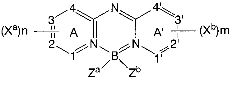
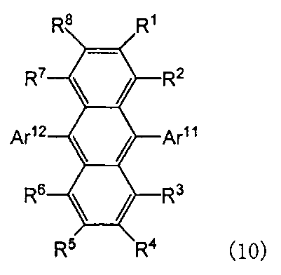
R1~R8は、それぞれ独立に、水素原子、置換もしくは無置換の環形成炭素数6~50のアリール基、置換もしくは無置換の環形成原子数5~50の複素環基、置換もしくは無置換の炭素数1~50のアルキル基、置換もしくは無置換の環形成炭素数3~50のシクロアルキル基、置換もしくは無置換の炭素数1~50のアルコキシ基、置換もしくは無置換の炭素数7~50のアラルキル基、置換もしくは無置換の環形成炭素数6~50のアリールオキシ基、置換もしくは無置換の環形成炭素数6~50のアリールチオ基、置換もしくは無置換の炭素数2~50のアルコキシカルボニル基、置換もしくは無置換のシリル基、カルボキシル基、ハロゲン原子、シアノ基、ニトロ基及びヒドロキシル基から選ばれる基である。 In the formula (10), Ar 11 and Ar 12 are each independently a substituted or unsubstituted aryl group having 6 to 50 ring carbon atoms or a heterocyclic group having 5 to 50 ring atoms,
R 1 to R 8 each independently represents a hydrogen atom, a substituted or unsubstituted aryl group having 6 to 50 ring carbon atoms, a substituted or unsubstituted heterocyclic group having 5 to 50 ring atoms, substituted or unsubstituted Substituted alkyl group having 1 to 50 carbon atoms, substituted or unsubstituted cycloalkyl group having 3 to 50 ring carbon atoms, substituted or unsubstituted alkoxy group having 1 to 50 carbon atoms, substituted or unsubstituted carbon number 7 -50 aralkyl group, substituted or unsubstituted aryloxy group having 6 to 50 ring carbon atoms, substituted or unsubstituted arylthio group having 6 to 50 ring carbon atoms, substituted or unsubstituted 2 to 50 carbon atoms It is a group selected from an alkoxycarbonyl group, a substituted or unsubstituted silyl group, a carboxyl group, a halogen atom, a cyano group, a nitro group and a hydroxyl group.
当該アントラセン誘導体は、式(10)におけるAr11及びAr12が、それぞれ独立に、置換もしくは無置換の環形成炭素数10~50の縮合アリール基となっている。当該アントラセン誘導体としては、Ar11及びAr12が同一の置換もしくは無置換の縮合アリール基である場合、及び異なる置換もしくは無置換の縮合アリール基である場合に分けることができる。
具体的には、下記式(2-1)~(2-3)で表されるアントラセン誘導体、及び式(10)におけるAr11及びAr12が異なる置換もしくは無置換の縮合アリール基であるアントラセン誘導体が挙げられる。 (Anthracene derivative (A))
In the anthracene derivative, Ar 11 and Ar 12 in Formula (10) are each independently a substituted or unsubstituted condensed aryl group having 10 to 50 ring carbon atoms. The anthracene derivative can be classified into a case where Ar 11 and Ar 12 are the same substituted or unsubstituted condensed aryl group and a case where they are different substituted or unsubstituted condensed aryl groups.
Specifically, anthracene derivatives represented by the following formulas (2-1) to (2-3), and anthracene derivatives in which Ar 11 and Ar 12 in formula (10) are different substituted or unsubstituted condensed aryl groups Is mentioned.

R11は水素原子、置換もしくは無置換の環形成炭素数6~50のアリール基、置換もしくは無置換の環形成原子数5~50の複素環基、置換もしくは無置換の炭素数1~50のアルキル基、置換もしくは無置換の環形成炭素数3~50のシクロアルキル基、置換もしくは無置換の炭素数1~50のアルコキシ基、置換もしくは無置換の炭素数7~50のアラルキル基、置換もしくは無置換の環形成炭素数6~50のアリールオキシ基、置換もしくは無置換の環形成炭素数6~50のアリールチオ基、置換もしくは無置換の炭素数2~50のアルコキシカルボニル基、置換もしくは無置換のシリル基、カルボキシル基、ハロゲン原子、シアノ基、ニトロ基及びヒドロキシル基から選ばれる基であり、
aは0~9の整数である。aが2以上の整数の場合、複数あるR11は、2つの置換もしくは無置換のフェナントレニル基が同一であることを条件に、それぞれが同一でも異なっていてもよい。) (In the formula (2-1), R 1 to R 8 are the same as above,
R 11 is a hydrogen atom, a substituted or unsubstituted aryl group having 6 to 50 ring carbon atoms, a substituted or unsubstituted heterocyclic group having 5 to 50 ring atoms, a substituted or unsubstituted carbon group having 1 to 50 carbon atoms. An alkyl group, a substituted or unsubstituted cycloalkyl group having 3 to 50 carbon atoms, a substituted or unsubstituted alkoxy group having 1 to 50 carbon atoms, a substituted or unsubstituted aralkyl group having 7 to 50 carbon atoms, substituted or Unsubstituted aryloxy group having 6 to 50 ring carbon atoms, substituted or unsubstituted arylthio group having 6 to 50 ring carbon atoms, substituted or unsubstituted alkoxycarbonyl group having 2 to 50 carbon atoms, substituted or unsubstituted A silyl group, a carboxyl group, a halogen atom, a cyano group, a nitro group and a hydroxyl group,
a is an integer of 0 to 9. When a is an integer of 2 or more, a plurality of R 11 s may be the same or different on condition that two substituted or unsubstituted phenanthrenyl groups are the same. )

bは1~7の整数である。bが2以上の整数の場合、複数あるR11は、2つの置換もしくは無置換の2-ナフチル基が同一であることを条件に、それぞれが同一でも異なっていてもよい。) (In the formula (2-2), R 1 to R 8 and R 11 are the same as above,
b is an integer of 1 to 7. When b is an integer of 2 or more, a plurality of R 11 may be the same or different on condition that two substituted or unsubstituted 2-naphthyl groups are the same. )
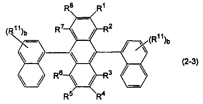
具体的には、Ar11が1-ナフチル基、及びAr12が2-ナフチル基である場合、Ar11が1-ナフチル基及びAr12が9-フェナントリル基である場合、並びにAr11が2-ナフチル基及びAr12が9-フェナントリル基である場合である。 As an anthracene derivative in which Ar 11 and Ar 12 in formula (10) are different substituted or unsubstituted condensed aryl groups, Ar 11 and Ar 12 are substituted or unsubstituted 9-phenanthrenyl group, substituted or unsubstituted 1 -It is preferably either a naphthyl group or a substituted or unsubstituted 2-naphthyl group.
Specifically, when Ar 11 is a 1-naphthyl group and Ar 12 is a 2-naphthyl group, Ar 11 is a 1-naphthyl group and Ar 12 is a 9-phenanthryl group, and Ar 11 is 2- This is the case where the naphthyl group and Ar 12 are a 9-phenanthryl group.
当該アントラセン誘導体は、式(10)におけるAr11及びAr12の一方が置換もしくは無置換のフェニル基であり、他方が置換もしくは無置換の環形成炭素数10~50の縮合アリール基となっている。当該アントラセン誘導体としては、具体的には、下記式(2-4)及び(2-5)で表されるアントラセン誘導体が挙げられる。 (Anthracene derivative (B))
In the anthracene derivative, one of Ar 11 and Ar 12 in formula (10) is a substituted or unsubstituted phenyl group, and the other is a substituted or unsubstituted condensed aryl group having 10 to 50 ring carbon atoms. . Specific examples of the anthracene derivative include anthracene derivatives represented by the following formulas (2-4) and (2-5).

Ar6は置換もしくは無置換の環形成炭素数6~50のアリール基、置換もしくは無置換の炭素数1~50のアルキル基、置換もしくは無置換の環形成炭素数3~50のシクロアルキル基、置換もしくは無置換の炭素数7~50のアラルキル基、置換もしくは無置換の環形成原子数5~50の複素環基、9,9-ジメチルフルオレン-1-イル基、9,9-ジメチルフルオレン-2-イル基、9,9-ジメチルフルオレン-3-イル基、9,9-ジメチルフルオレン-4-イル基、ジベンゾフラン-1-イル基、ジベンゾフラン-2-イル基、ジベンゾフラン-3-イル基、又はジベンゾフラン-4-イル基である。また、Ar6はそれが結合しているベンゼン環と共に、置換もしくは無置換のフルオレニル基や置換もしくは無置換のジベンゾフラニル基等の環を形成していてもよい。bが2以上の整数の場合、複数あるR11は、それぞれが同一でも異なっていてもよい。) (In the formula (2-4), R 1 to R 8 , R 11 and b are the same as above,
Ar 6 represents a substituted or unsubstituted aryl group having 6 to 50 ring carbon atoms, a substituted or unsubstituted alkyl group having 1 to 50 carbon atoms, a substituted or unsubstituted cycloalkyl group having 3 to 50 ring carbon atoms, Substituted or unsubstituted aralkyl group having 7 to 50 carbon atoms, substituted or unsubstituted heterocyclic group having 5 to 50 ring atoms, 9,9-dimethylfluoren-1-yl group, 9,9-dimethylfluorene- 2-yl group, 9,9-dimethylfluoren-3-yl group, 9,9-dimethylfluoren-4-yl group, dibenzofuran-1-yl group, dibenzofuran-2-yl group, dibenzofuran-3-yl group, Or a dibenzofuran-4-yl group. Ar 6 may form a ring such as a substituted or unsubstituted fluorenyl group or a substituted or unsubstituted dibenzofuranyl group together with a benzene ring to which Ar 6 is bonded. When b is an integer of 2 or more, the plurality of R 11 may be the same or different. )
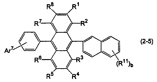
Ar7は、置換もしくは無置換の環形成炭素数6~50のアリール基、置換もしくは無置換の環形成原子数5~50の複素環基、置換もしくは無置換の炭素数1~50のアルキル基、置換もしくは無置換の環形成炭素数3~50のシクロアルキル基、置換もしくは無置換の炭素数7~50のアラルキル基、ジベンゾフラン-1-イル基、ジベンゾフラン-2-イル基、ジベンゾフラン-3-イル基、又はジベンゾフラン-4-イル基である。また、Ar7はそれが結合しているベンゼン環と共に、置換もしくは無置換のフルオレニル基や置換もしくは無置換のジベンゾフラニル基等の環を形成していてもよい。bが2以上の整数の場合、複数あるR11は、それぞれが同一でも異なっていてもよい。) (In the formula (2-5), R 1 to R 8 , R 11 and b are the same as above,
Ar 7 is a substituted or unsubstituted aryl group having 6 to 50 ring carbon atoms, a substituted or unsubstituted heterocyclic group having 5 to 50 ring atoms, or a substituted or unsubstituted alkyl group having 1 to 50 carbon atoms. Substituted or unsubstituted ring-forming cycloalkyl group having 3 to 50 carbon atoms, substituted or unsubstituted aralkyl group having 7 to 50 carbon atoms, dibenzofuran-1-yl group, dibenzofuran-2-yl group, dibenzofuran-3- An yl group or a dibenzofuran-4-yl group. Ar 7 may form a ring such as a substituted or unsubstituted fluorenyl group or a substituted or unsubstituted dibenzofuranyl group together with a benzene ring to which Ar 7 is bonded. When b is an integer of 2 or more, the plurality of R 11 may be the same or different. )
当該アントラセン誘導体は、下記式(2-6)で表され、具体的には、下記式(2-6-1)、(2-6-2)及び(2-6-3)のいずれかで表される誘導体であることが好ましい。
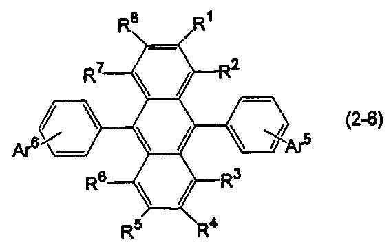
The anthracene derivative is represented by the following formula (2-6), specifically, any one of the following formulas (2-6-1), (2-6-2), and (2-6-3) It is preferable that it is a derivative represented.
Ar5は置換もしくは無置換の環形成炭素数6~50のアリール基、置換もしくは無置換の炭素数1~50のアルキル基、置換もしくは無置換の環形成炭素数3~50のシクロアルキル基、置換もしくは無置換の炭素数7~50のアラルキル基、又は置換もしくは無置換の環形成原子数5~50の複素環基であり、Ar5とAr6はそれぞれ独立に選択される。)
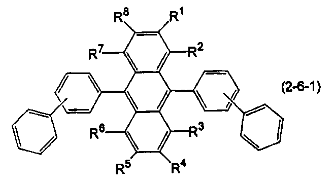
Ar 5 is a substituted or unsubstituted aryl group having 6 to 50 ring carbon atoms, a substituted or unsubstituted alkyl group having 1 to 50 carbon atoms, a substituted or unsubstituted cycloalkyl group having 3 to 50 ring carbon atoms, A substituted or unsubstituted aralkyl group having 7 to 50 carbon atoms, or a substituted or unsubstituted heterocyclic group having 5 to 50 ring atoms, and Ar 5 and Ar 6 are independently selected. )
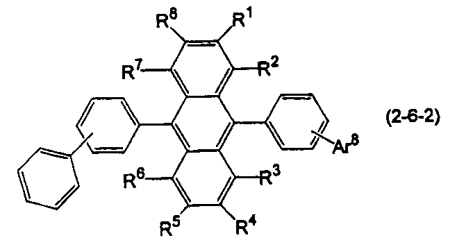
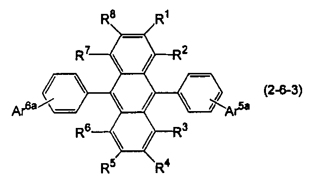
Ar5a及びAr6aはそれぞれ独立に、置換もしくは無置換の環形成炭素数10~20の縮合アリール基である。) (In the formula (2-6-3), R 1 to R 8 are the same as in the formula (10).
Ar 5a and Ar 6a are each independently a substituted or unsubstituted condensed aryl group having 10 to 20 ring carbon atoms. )
図3CはAh<Adを満たすドーパントとAh>Adを満たすドーパントの双方を発光層が含む場合を示している。このような場合は、電子、正孔のいずれもほどよくトラップされ、結果として発光層内全域で再結合が起きる。従って、陰極側においても多く再結合が起きており、3重項エネルギーの大きな障壁層を設けることにより効率よくTTF現象が起きるようになる。 (2) When a dopant satisfying Ah <Ad and a dopant satisfying Ah> Ad coexist FIG. 3C shows a case where the light emitting layer includes both a dopant satisfying Ah <Ad and a dopant satisfying Ah> Ad. In such a case, both electrons and holes are trapped reasonably, and as a result, recombination occurs throughout the light emitting layer. Therefore, a lot of recombination occurs on the cathode side, and the TTF phenomenon efficiently occurs by providing a barrier layer having a large triplet energy.
この場合には、電子注入層のアフィニティAe-障壁層のアフィニティAb<0.2eVであることが好ましい。これを満たさない場合、電子注入層から障壁層への電子注入が損なわれ、電子輸送帯域に電子が蓄積し、高電圧化を引き起こすとともに、蓄積電子が3重項励起子と衝突してエネルギーがクエンチされる。
ここで、本発明における障壁層を構成する材料の電子移動度は、電界強度0.04~0.5MV/cmの範囲において、10-6cm2/Vs以上であることが望ましい。
さらに、本発明における電子注入層は、電界強度0.04~0.5MV/cmの範囲において、10-6cm2/Vs以上であることが望ましい。発光層への電子注入を促進し、発光層内の励起子密度を高め、TTF現象を効率よく起こすためである。 (1) The electron transport zone has a laminated structure of two or more different materials, and an electron injection layer for efficiently receiving electrons from the cathode is provided between the barrier layer and the cathode. Specific examples of the electron injection layer include nitrogen-containing heterocyclic derivatives.
In this case, it is preferable that the affinity Ae of the electron injection layer−the affinity Ab of the barrier layer <0.2 eV. If this is not satisfied, electron injection from the electron injection layer to the barrier layer is impaired, electrons are accumulated in the electron transport band, causing a high voltage, and the accumulated electrons collide with triplet excitons, resulting in energy consumption. Quenched.
Here, the electron mobility of the material constituting the barrier layer in the present invention is preferably 10 −6 cm 2 / Vs or more in the range of electric field strength of 0.04 to 0.5 MV / cm.
Further, the electron injection layer in the present invention is desirably 10 −6 cm 2 / Vs or more in the range of electric field strength of 0.04 to 0.5 MV / cm. This is because the electron injection into the light emitting layer is promoted, the exciton density in the light emitting layer is increased, and the TTF phenomenon is efficiently caused.
ドナー性金属化合物とは、上記のドナー性金属を含む化合物であり、好ましくはアルカリ金属、アルカリ土類金属又は希土類金属を含む化合物であり、より好ましくはこれらの金属のハロゲン化物、酸化物、炭酸塩、ホウ酸塩である。例えば、MOx(Mはドナー性金属、xは0.5~1.5)、MFx(xは1~3)、M(CO3)x(xは0.5~1.5)で表される化合物である。 The donor metal means a metal having a work function of 3.8 eV or less, preferably an alkali metal, an alkaline earth metal, or a rare earth metal, and more preferably Cs, Li, Na, Sr, K, Mg, Ca, Ba. , Yb, Eu and Ce.
The donor metal compound is a compound containing the above donor metal, preferably a compound containing an alkali metal, an alkaline earth metal or a rare earth metal, and more preferably a halide, oxide or carbonic acid of these metals. Salt, borate. For example, MOx (M is a donor metal, x is 0.5 to 1.5), MFx (x is 1 to 3), M (CO 3 ) x (x is 0.5 to 1.5) It is a compound.
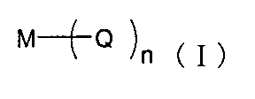
上記のドナーは一種単独で使用してもよいし、二種以上を組み合わせて使用してもよい。 Specific examples of the donor metal complex include a tungsten turbine described in JP-A-2005-72012. Further, phthalocyanine compounds whose central metals are alkali metals and alkaline earth metals described in JP-A-11-345687 can also be used as donor metal complexes.
Said donor may be used individually by 1 type, and may be used in combination of 2 or more type.
Ra-Ar101-Rb ・・・(A)
Ra-Ar101-Ar102-Rb ・・・(B)
Ra-Ar101-Ar102-Ar103-Rb ・・・(C) Specific examples of materials excellent in oxidation durability include hydrocarbon aromatic compounds, particularly polycyclic aromatic compounds represented by the following formulas (A), (B) and (C) described in Japanese Patent Application No. 2009-090379 It is desirable that the compound be one or more compounds selected from the group consisting of:
Ra-Ar 101 -Rb (A)
Ra-Ar 101 -Ar 102 -Rb (B)
Ra-Ar 101 -Ar 102 -Ar 103 -Rb (C)
多環芳香族骨格部の置換基としては、例えば、ハロゲン原子、ヒドロキシル基、置換若しくは無置換のアミノ基、ニトロ基、シアノ基、置換若しくは無置換のアルキル基、置換若しくは無置換のアルケニル基、置換若しくは無置換のシクロアルキル基、置換若しくは無置換のアルコキシ基、置換若しくは無置換の芳香族炭化水素基、置換若しくは無置換の芳香族複素環基、置換若しくは無置換のアラルキル基、置換若しくは無置換のアリールオキシ基、置換若しくは無置換のアルコキシカルボニル基、又は、カルボキシル基が挙げられる。芳香族炭化水素基の好ましい例としては、ナフタレン、フェナントレン、フルオレン、クリセン、フルオランテン及びトリフェニレンを挙げることができる。多環芳香族骨格部が複数の置換基を有する場合、それらが環を形成していてもよい。 The polycyclic aromatic skeleton of the polycyclic aromatic compound may have a substituent.
Examples of the substituent of the polycyclic aromatic skeleton include, for example, a halogen atom, a hydroxyl group, a substituted or unsubstituted amino group, a nitro group, a cyano group, a substituted or unsubstituted alkyl group, a substituted or unsubstituted alkenyl group, Substituted or unsubstituted cycloalkyl group, substituted or unsubstituted alkoxy group, substituted or unsubstituted aromatic hydrocarbon group, substituted or unsubstituted aromatic heterocyclic group, substituted or unsubstituted aralkyl group, substituted or unsubstituted Examples thereof include a substituted aryloxy group, a substituted or unsubstituted alkoxycarbonyl group, and a carboxyl group. Preferable examples of the aromatic hydrocarbon group include naphthalene, phenanthrene, fluorene, chrysene, fluoranthene and triphenylene. When the polycyclic aromatic skeleton has a plurality of substituents, they may form a ring.
式(1)で表される化合物としては、例えば、置換若しくは無置換のフェナントレン、クリセンの単体又は誘導体等が挙げられる。
式(2)で表される化合物としては、例えば、置換若しくは無置換のアセナフチレン、アセナフテン、フルオランテンの単体又は誘導体等が挙げられる。
式(3)で表される化合物としては、例えば、置換若しくは無置換のベンゾフルオランテンの単体又は誘導体等が挙げられる。
式(4)で表される化合物としては、例えば、置換若しくは無置換のナフタレンの単体又は誘導体等が挙げられる。 In the formulas (1) to (4), Ar 1 to Ar 5 represent a substituted or unsubstituted condensed ring structure having 4 to 16 nuclear carbon atoms.
Examples of the compound represented by the formula (1) include a substituted or unsubstituted phenanthrene, a simple substance or a derivative of chrysene.
Examples of the compound represented by the formula (2) include substituted or unsubstituted acenaphthylene, acenaphthene, fluoranthene alone or derivatives.
Examples of the compound represented by the formula (3) include a single or derivative of a substituted or unsubstituted benzofluoranthene.
Examples of the compound represented by the formula (4) include substituted or unsubstituted naphthalene alone or derivatives.

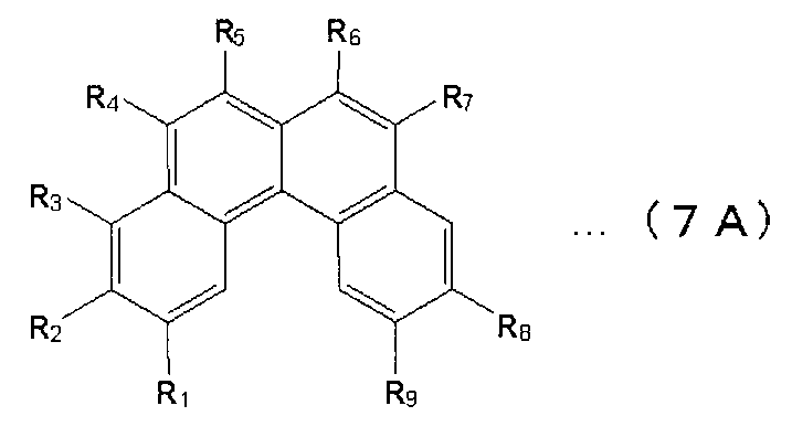
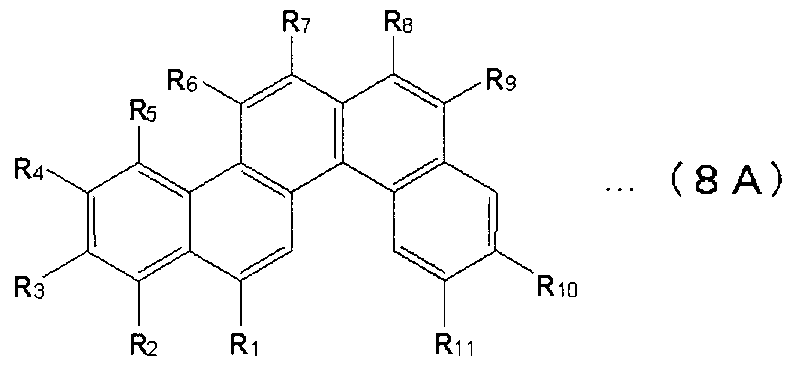

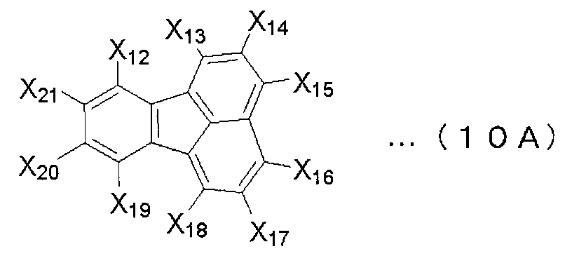
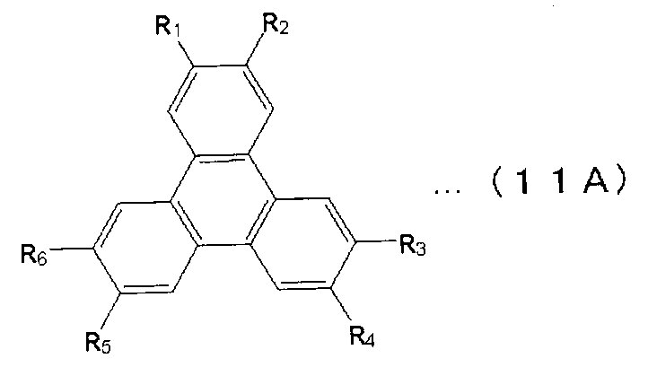
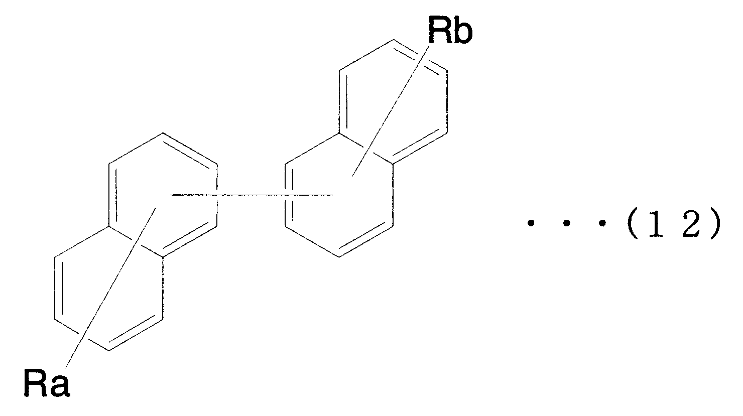
式(12)中、Ra、Rbは、フルオレン環、フェナントレン環、トリフェニレン環、ベンゾフェナントレン環、ジベンゾフェナントレン環、ベンゾトリフェニレン環、フルオランテン環、ベンゾクリセン環、ベンゾ[b]フルオランテン環及びピセン環から選択される基であることが好ましい。 The polycyclic aromatic compound may be represented by the following formula (12).
In the formula (12), Ra and Rb are selected from fluorene ring, phenanthrene ring, triphenylene ring, benzophenanthrene ring, dibenzophenanthrene ring, benzotriphenylene ring, fluoranthene ring, benzochrysene ring, benzo [b] fluoranthene ring and picene ring. It is preferably a group.
電子移動度=(障壁層材料の膜厚)2/(応答時間・電圧) The mobility measurement by impedance spectroscopy will be described. A barrier layer material having a thickness of preferably about 100 nm to 200 nm is sandwiched between the anode and the cathode, and a minute AC voltage of 100 mV or less is applied while applying a bias DC voltage. The AC current value (absolute value and phase) flowing at this time is measured. This measurement is performed while changing the frequency of the AC voltage, and the complex impedance (Z) is calculated from the current value and the voltage value. At this time, the frequency dependence of the imaginary part (ImM) of the modulus M = iωZ (i: imaginary unit, ω: angular frequency) is obtained, and the reciprocal of the frequency ω at which ImM is the maximum value is determined by the electron conducting in the barrier layer. It is defined as response time. Then, the electron mobility is calculated by the following formula.
Electron mobility = (film thickness of barrier layer material) 2 / (response time / voltage)
ホスト、ドーパント及び障壁層材料の三重項エネルギーが所定の関係を満たすことにより、全発光に対するTTF由来の発光強度比を30%以上とすることができ、従来知られていた蛍光素子では達成できなかった高効率化を可能とすることができる。 <Measurement of TTF ratio>
When the triplet energy of the host, dopant, and barrier layer material satisfies the predetermined relationship, the ratio of TTF-derived emission intensity to the total emission can be increased to 30% or more, which cannot be achieved with a conventionally known fluorescent element. High efficiency can be achieved.


本発明の素子は、発光層を含む有機層ユニットを少なくとも2つ有するタンデム素子構成とすることができる。2つの発光層の間には中間層(中間導電層、電化発生層、CGLとも呼ぶ)が介在する。ユニット毎に電子輸送帯域を設けることができる。少なくとも1つの発光層が蛍光発光層でありその発光層を含むユニットが上記の要件を満たす。具体的な積層順の例を以下に示す。また、下記発光層は、複数の発光層の積層体であってもよく、後述する第3の実施形態の電荷障壁層を含む一の有機層ユニットであっても良い。
陽極/蛍光発光層/中間層/蛍光発光層/障壁層/陰極
陽極/蛍光発光層/障壁層/中間層/蛍光発光層/陰極
陽極/蛍光発光層/障壁層/中間層/蛍光発光層/障壁層/陰極
陽極/りん光発光層/中間層/蛍光発光層/障壁層/陰極
陽極/蛍光発光層/障壁層/中間層/りん光発光層/陰極 <Second Embodiment>
The element of the present invention can have a tandem element configuration having at least two organic layer units including a light emitting layer. An intermediate layer (also referred to as an intermediate conductive layer, a charge generation layer, or CGL) is interposed between the two light emitting layers. An electron transport zone can be provided for each unit. At least one light emitting layer is a fluorescent light emitting layer, and a unit including the light emitting layer satisfies the above requirements. An example of a specific stacking order is shown below. Further, the following light emitting layer may be a laminate of a plurality of light emitting layers, or may be one organic layer unit including a charge barrier layer of a third embodiment described later.
Anode / fluorescent layer / intermediate layer / fluorescent layer / barrier layer / cathode Anode / fluorescent layer / barrier layer / intermediate layer / fluorescent layer / cathode Anode / fluorescent layer / barrier layer / intermediate layer / fluorescent layer / Barrier layer / cathode Anode / phosphorescent layer / intermediate layer / fluorescent layer / barrier layer / cathode Anode / fluorescent layer / barrier layer / intermediate layer / phosphorescent layer / cathode
本実施形態では、陽極と、複数の発光層と、電子輸送帯域と、陰極をこの順に備え、複数の発光層のいずれか二つの発光層の間に電荷障壁層を有し、電荷障壁層に接する発光層が蛍光発光層であり、上記の要件を満たす。 <Third Embodiment>
In this embodiment, an anode, a plurality of light emitting layers, an electron transport zone, and a cathode are provided in this order, and a charge barrier layer is provided between any two light emitting layers of the plurality of light emitting layers, The light emitting layer in contact with it is a fluorescent light emitting layer and satisfies the above requirements.
陽極/第1発光層/電荷障壁層/第2発光層/電子輸送帯域/陰極
陽極/第1発光層/電荷障壁層/第2発光層/第3発光層/電子輸送帯域/陰極
尚、陽極と第1発光層の間には、他の実施形態と同様に正孔輸送帯域を設けることが好ましい。 A specific example of such a configuration is shown below.
Anode / first light emitting layer / charge barrier layer / second light emitting layer / electron transport zone / cathode Anode / first light emitting layer / charge barrier layer / second light emitting layer / third light emitting layer / electron transport zone / cathode As in the other embodiments, it is preferable to provide a hole transport zone between the first light emitting layer and the first light emitting layer.
この有機EL素子2は、陽極と、第1発光層、第2発光層、第3発光層と、電子輸送帯域と、陰極4をこの順に備え、第1発光層と第2発光層の間には、電荷障壁層がある。電子輸送帯域は障壁層からなる。第3発光層が本発明の要件を満たす蛍光発光層である。第1発光層、第2発光層は蛍光型でも燐光型でもよい。 FIG. 7 shows an example of the organic EL element according to this embodiment. The upper diagram of FIG. 7 shows the device configuration and the HOMO and LUMO energy levels of each layer. The figure below shows the relationship between the energy gap between the third light emitting layer and the barrier layer.
The
本実施形態では、青色画素、緑色画素、赤色画素を、基板上に並べて設ける。これら3色の画素のうち、青色画素及び/又は緑色画素が第1の実施形態の構成を有する。 <Fourth Embodiment>
In this embodiment, blue pixels, green pixels, and red pixels are provided side by side on the substrate. Of these three color pixels, a blue pixel and / or a green pixel have the configuration of the first embodiment.
この図に示す上面発光型有機EL素子3は、共通基板100上に、青色画素B、緑色画素G及び赤色画素Rが並列に形成されている。 FIG. 8 shows an example of the organic EL element according to this embodiment.
In the top emission organic EL element 3 shown in this figure, a blue pixel B, a green pixel G, and a red pixel R are formed in parallel on a
緑色画素Gは、陽極10、正孔輸送帯域50、緑色発光層20G、障壁層32からなる電子輸送帯域、陰極40、保護層70を基板100からこの順に備えている。
赤色画素Rは、陽極10、正孔輸送帯域50、赤色発光層20R、障壁層32からなる電子輸送帯域、陰極40、保護層70を基板100からこの順に備えている。
それぞれの隣接する画素の陽極間に絶縁膜200が形成され、画素間の絶縁を保持している。
有機EL素子3では、障壁層が青色画素B、赤色画素R、緑色画素Gに共通に設けられている。 The blue pixel B includes an
The green pixel G includes an
The red pixel R includes an
An insulating
In the organic EL element 3, the barrier layer is provided in common for the blue pixel B, the red pixel R, and the green pixel G.
一方、燐光発光層においては、三重項励起子を発光層内に閉じ込める効果を得ることが可能であり、三重項エネルギーの拡散を防ぎ、燐光発光性ドーパントの発光効率の向上に寄与する。 The effect of the barrier layer is remarkable compared to the light emission efficiency obtained in the conventional blue fluorescent element, but the same effect of confining the triplet energy in the light emitting layer is obtained also in the green fluorescent element and the red fluorescent element. Therefore, improvement in luminous efficiency can be expected.
On the other hand, in the phosphorescent light-emitting layer, it is possible to obtain an effect of confining triplet excitons in the light-emitting layer, preventing triplet energy diffusion and contributing to the improvement of the luminous efficiency of the phosphorescent dopant.
発光層20B,G,Rと障壁層から構成される有機層は、図に示す構成に限定されず適宜変更できる。 The hole transport zone includes a hole transport layer, a hole transport layer, a hole injection layer, and the like. The hole transport zones may be common or different. In general, each hole transport zone has a configuration suitable for the emission color.
The organic layer composed of the
緑色発光層は、以下のホスト材料及びドーパント材料から構成されるのが好ましい。ホスト材料は、縮合芳香族環誘導体が好ましい。縮合芳香族環誘導体としては、アントラセン誘導体、ピレン誘導体等が、発光効率や発光寿命の点でさらに好ましい。 The host and the dopant that can be used in the present invention have been described above. In particular, each color light emitting layer will be described below.
The green light emitting layer is preferably composed of the following host material and dopant material. The host material is preferably a condensed aromatic ring derivative. As the condensed aromatic ring derivatives, anthracene derivatives, pyrene derivatives, and the like are more preferable in terms of light emission efficiency and light emission lifetime.
基板上に、銀合金層であるAPC(Ag-Pd-Cu)層(反射層)、酸化亜鉛膜(IZO)や酸化錫膜等の透明導電層をこの順に成膜する。続いて通常のリソグラフィ技術を用いて、レジストパターンをマスクに用いたエッチングにより、この導電材料層をパターニングし、陽極を形成する。次に、陽極の上にスピンコート法により、ポリイミド等の感光性樹脂からなる絶縁膜を塗布形成する。その後、露光、現像、硬化することで、陽極を露出させることにより青発光領域、緑発光領域、赤発光領域をパターンニングする。 The element of Embodiment 4 is produced as follows, for example.
A transparent conductive layer such as an APC (Ag—Pd—Cu) layer (reflection layer), a zinc oxide film (IZO), or a tin oxide film, which is a silver alloy layer, is formed on the substrate in this order. Subsequently, the conductive material layer is patterned by etching using a resist pattern as a mask by using a normal lithography technique to form an anode. Next, an insulating film made of a photosensitive resin such as polyimide is applied and formed on the anode by spin coating. Thereafter, the blue light emitting region, the green light emitting region, and the red light emitting region are patterned by exposing, developing and curing to expose the anode.
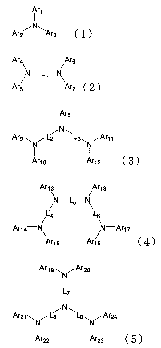
L1~L9は、各々独立して、置換もしくは無置換の環形成炭素数6~50のアリーレン基、又は置換もしくは無置換の環形成原子数5~50のヘテロアリーレン基を表わす。
Ar1~Ar24、L1~L9が有してもよい置換基は、炭素数1~15の直鎖状もしくは分岐状のアルキル基、環形成炭素数3~15のシクロアルキル基、炭素数1~15の直鎖状もしくは分岐状のアルキル基を有するトリアルキルシリル基、環形成炭素数6~14のアリール基を有するトリアリールシリル基、炭素数1~15の直鎖状もしくは分岐状のアルキル基及び環形成炭素数6~14のアリール基を有するアルキルアリールシリル基、環形成炭素数6~50のアリール基、環形成原子数5~50のヘテロアリール基、ハロゲン原子又はシアノ基である。隣接した複数の置換基は、互いに結合して、環を形成する飽和もしくは不飽和の2価の基を形成してもよい。) (In the formula, Ar 1 to Ar 24 each independently represents a substituted or unsubstituted aryl group having 6 to 50 ring carbon atoms or a substituted or unsubstituted heteroaryl group having 5 to 50 ring atoms. Represent.
L 1 to L 9 each independently represents a substituted or unsubstituted arylene group having 6 to 50 ring carbon atoms or a substituted or unsubstituted heteroarylene group having 5 to 50 ring atoms.
The substituents that Ar 1 to Ar 24 and L 1 to L 9 may have include a linear or branched alkyl group having 1 to 15 carbon atoms, a cycloalkyl group having 3 to 15 ring carbon atoms, carbon A trialkylsilyl group having a linear or branched alkyl group having 1 to 15 carbon atoms, a triarylsilyl group having an aryl group having 6 to 14 ring carbon atoms, a linear or branched carbon having 1 to 15 carbon atoms An alkylarylsilyl group having an alkyl group and an aryl group having 6 to 14 ring carbon atoms, an aryl group having 6 to 50 ring carbon atoms, a heteroaryl group having 5 to 50 ring atoms, a halogen atom or a cyano group is there. A plurality of adjacent substituents may be bonded to each other to form a saturated or unsaturated divalent group forming a ring. )
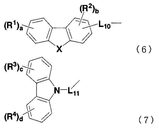
L10は、単結合、置換もしくは無置換の環形成炭素数6~50のアリーレン基、又は置換もしくは無置換の環形成原子数5~50のヘテロアリーレン基を表わす。
L11は、置換もしくは無置換の環形成炭素数6~50のアリーレン基、又は置換もしくは無置換の環形成原子数5~50のヘテロアリーレン基を表わす。
R1~R4は、各々独立して、炭素数1~15の直鎖状もしくは分岐状のアルキル基、環形成炭素数3~15のシクロアルキル基、炭素数1~15の直鎖状もしくは分岐状のアルキル基を有するトリアルキルシリル基、環形成炭素数6~14のアリール基を有するトリアリールシリル基、炭素数1~15の直鎖状もしくは分岐状のアルキル基及び環形成炭素数6~14のアリール基を有するアルキルアリールシリル基、環形成炭素数6~14のアリール基、環形成原子数5~50のヘテロアリール基、ハロゲン原子又はシアノ基を表す。また、隣接した複数のR1~R4は互いに結合して環を形成してもよい。
a、c、dは0~4の整数を表わす。
bは0~3の整数を表わす。) (In the formula, X represents an oxygen atom, a sulfur atom, or N—Ra, and Ra represents a linear or branched alkyl group having 1 to 15 carbon atoms, a cycloalkyl group having 3 to 15 ring carbon atoms, It represents an aryl group having 6 to 50 ring carbon atoms or a heteroaryl group having 5 to 50 ring atoms.
L 10 represents a single bond, a substituted or unsubstituted arylene group having 6 to 50 ring carbon atoms, or a substituted or unsubstituted heteroarylene group having 5 to 50 ring atoms.
L 11 represents a substituted or unsubstituted arylene group having 6 to 50 ring carbon atoms or a substituted or unsubstituted heteroarylene group having 5 to 50 ring atoms.
R 1 to R 4 are each independently a linear or branched alkyl group having 1 to 15 carbon atoms, a cycloalkyl group having 3 to 15 ring carbon atoms, a straight chain having 1 to 15 carbon atoms, A trialkylsilyl group having a branched alkyl group, a triarylsilyl group having an aryl group having 6 to 14 ring carbon atoms, a linear or branched alkyl group having 1 to 15 carbon atoms, and a ring carbon number of 6 An alkylarylsilyl group having an aryl group of ˜14, an aryl group having 6 to 14 ring carbon atoms, a heteroaryl group having 5 to 50 ring atoms, a halogen atom or a cyano group; A plurality of adjacent R 1 to R 4 may be bonded to each other to form a ring.
a, c and d each represents an integer of 0 to 4;
b represents an integer of 0 to 3. )
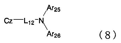
L12は置換もしくは無置換の環形成炭素数6~50のアリーレン基、又は置換もしくは無置換の環形成原子数5~50のヘテロアリーレン基を表わす。
Ar25及びAr26は、各々独立して、置換もしくは無置換の環形成炭素数6~50のアリール基、又は置換もしくは無置換の環形成原子数5~50のヘテロアリール基を表わす。) (In the formula, Cz represents a substituted or unsubstituted carbazolyl group.
L 12 represents a substituted or unsubstituted arylene group having 6 to 50 ring carbon atoms or a substituted or unsubstituted heteroarylene group having 5 to 50 ring atoms.
Ar 25 and Ar 26 each independently represents a substituted or unsubstituted aryl group having 6 to 50 ring carbon atoms or a substituted or unsubstituted heteroaryl group having 5 to 50 ring atoms. )

e、fは0~4の整数を表わす。
L12、Ar25及びAr26は、式(8)におけるL12、Ar25及びAr26と同義である。) (Wherein R 5 and R 6 are each independently a linear or branched alkyl group having 1 to 15 carbon atoms, a cycloalkyl group having 3 to 15 ring carbon atoms, or a
e and f each represents an integer of 0 to 4.
L 12, Ar 25 and Ar 26 are the same meaning as L 12, Ar 25 and Ar 26 in the formula (8). )
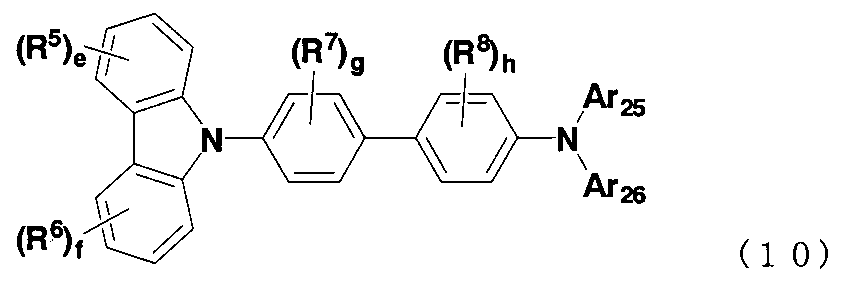
g、hは0~4の整数を表わす。
R5、R6、e、f、Ar25及びAr26は、式(9)におけるR5、R6、e、f、Ar25及びAr26と同義である。) (Wherein R 7 and R 8 are each independently a linear or branched alkyl group having 1 to 15 carbon atoms, a cycloalkyl group having 3 to 15 ring carbon atoms, or a
g and h each represents an integer of 0 to 4.
R 5, R 6, e, f, Ar 25 and Ar 26 are the same meaning as R 5, R 6, e, f, Ar 25 and Ar 26 in the formula (9). )
実施例及び比較例で使用した材料と物性値は以下の通りである。
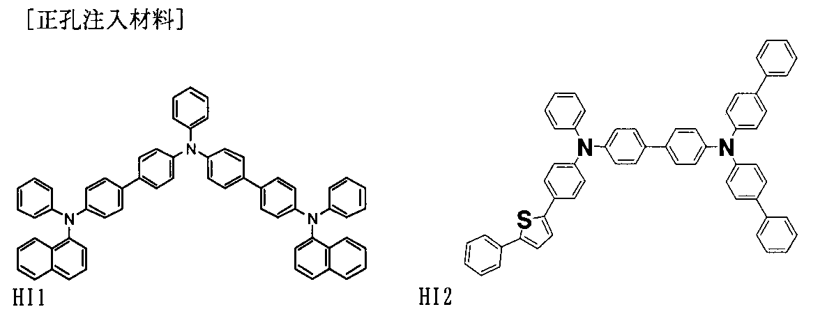
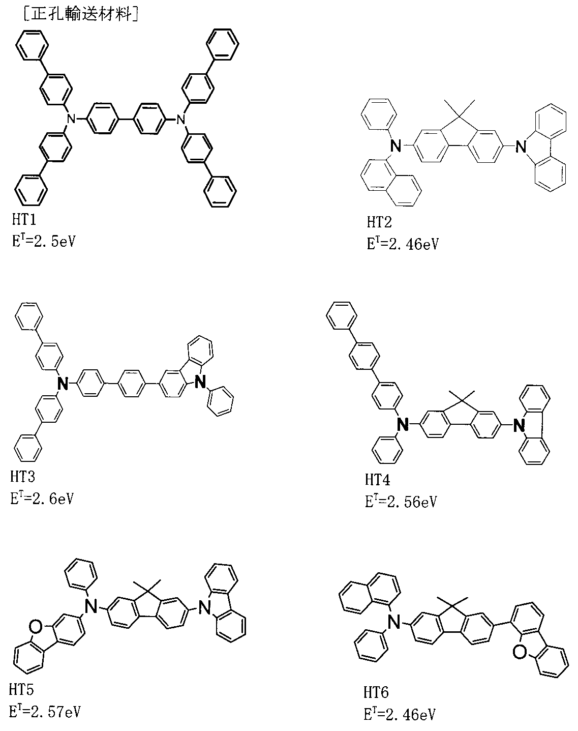
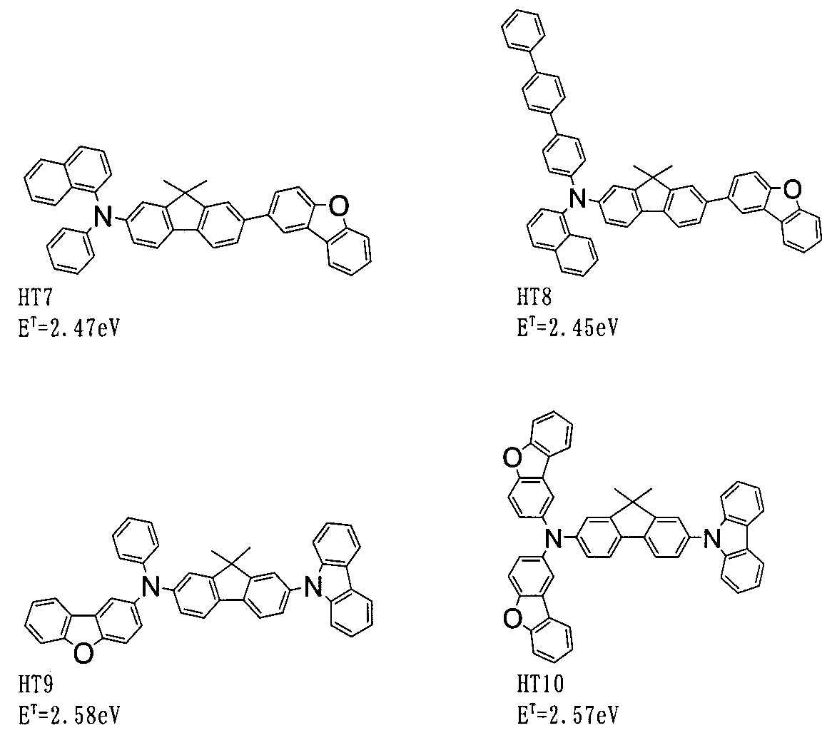


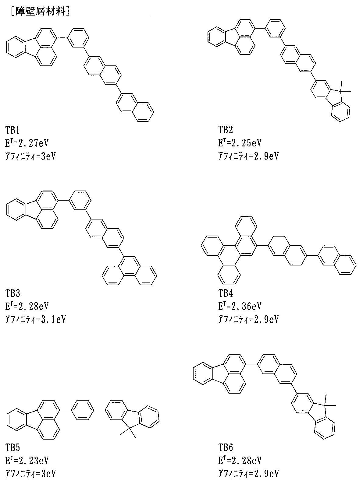
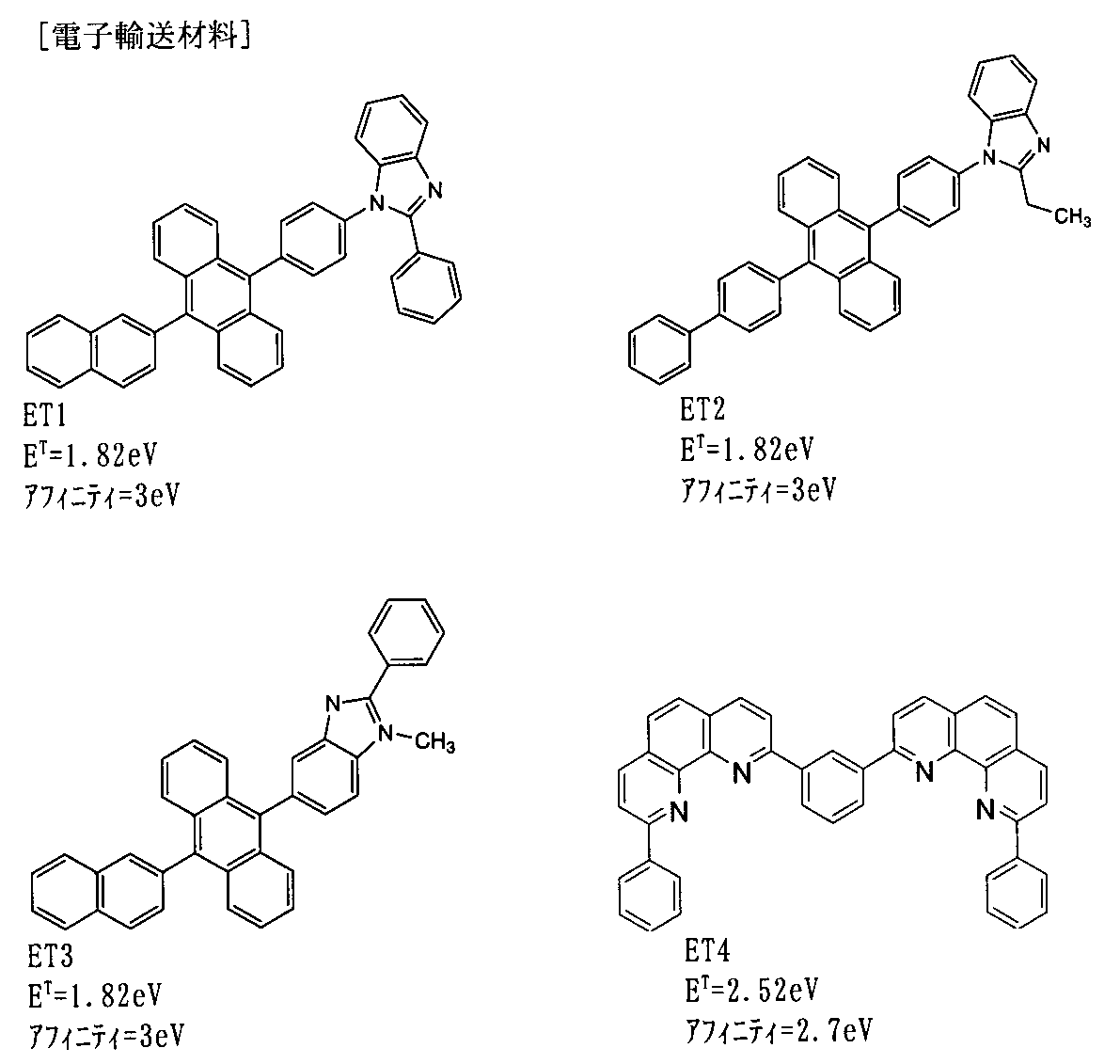
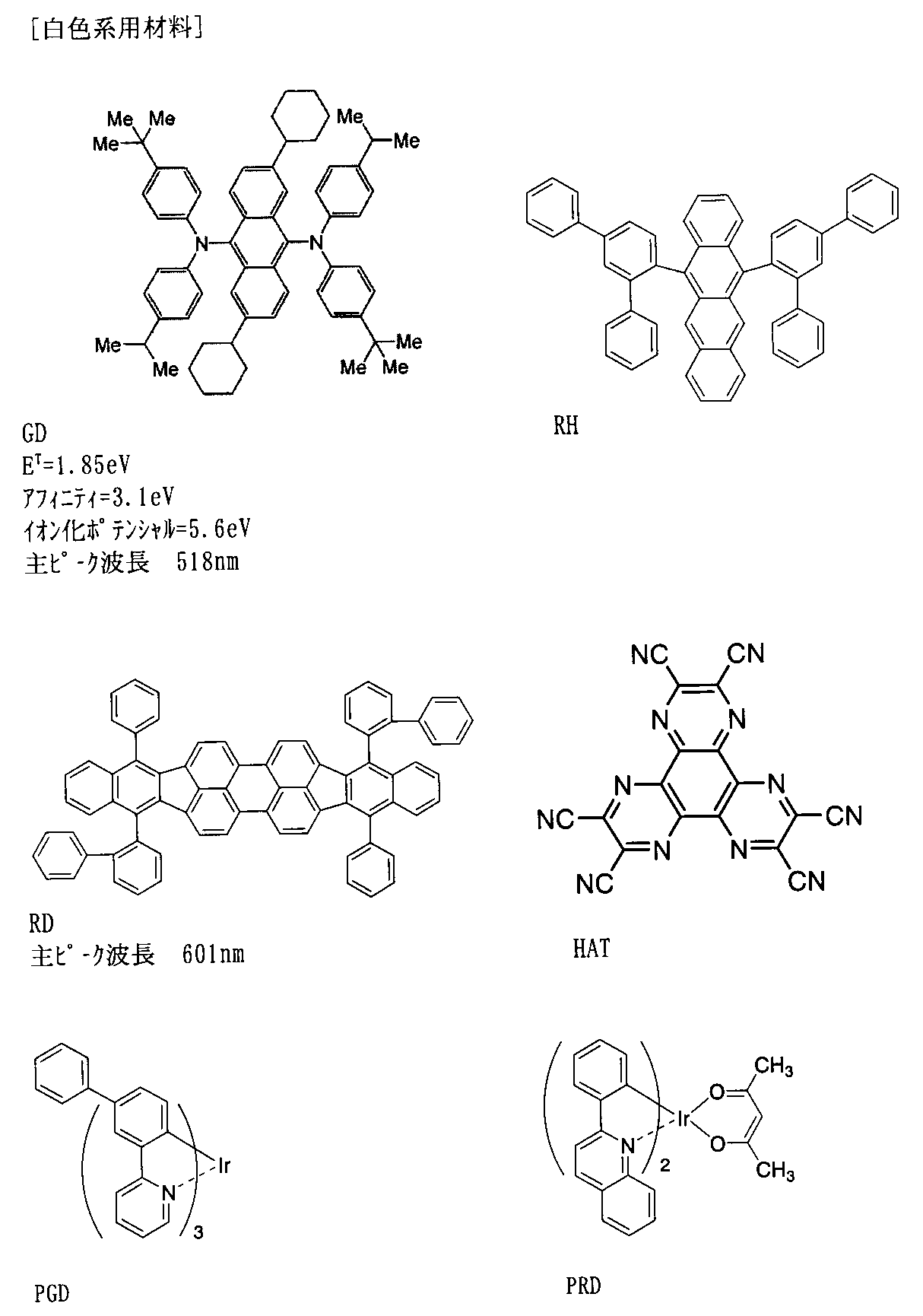

(1)3重項エネルギー(ET)
市販の装置F-4500(日立社製)を用いて測定した。ETの換算式は以下の通りである。
換算式 ET(eV)=1239.85/λedge
「λedge」とは、縦軸にりん光強度、横軸に波長をとって、りん光スペクトルを表したときに、りん光スペクトルの短波長側の立ち上がりに対して接線を引き、その接線と横軸の交点の波長値を意味する。単位:nm。 The measuring method of the above physical property values is as follows.
(1) Triplet energy (E T )
The measurement was performed using a commercially available apparatus F-4500 (manufactured by Hitachi). Conversion formula of E T is as follows.
Conversion formula E T (eV) = 1239.85 / λ edge
“Λ edge ” is a phosphorescence spectrum with the vertical axis representing the phosphorescence intensity and the horizontal axis representing the wavelength, and a tangent line is drawn with respect to the short wavelength side rise of the phosphorescence spectrum. It means the wavelength value at the intersection of the horizontal axis. Unit: nm.
大気下光電子分光装置(理研計器(株)社製:AC-1)を用いて測定した。具体的には、材料に光を照射し、その際に電荷分離によって生じる電子量を測定することにより測定した。 (2) Ionization potential The ionization potential was measured using an atmospheric photoelectron spectrometer (manufactured by Riken Keiki Co., Ltd .: AC-1). Specifically, the measurement was performed by irradiating the material with light and measuring the amount of electrons generated by charge separation at that time.
イオン化ポテンシャルとエネルギーギャップの測定値から算出した。エネルギーギャップはベンゼン中の吸収スペクトルの吸収端から測定した。具体的には、市販の可視・紫外分光光度計を用いて、吸収スペクトルを測定し、そのスペクトルが立ち上がり始める波長から算出した。 (3) Affinity Calculated from measured values of ionization potential and energy gap. The energy gap was measured from the absorption edge of the absorption spectrum in benzene. Specifically, the absorption spectrum was measured using a commercially available visible / ultraviolet spectrophotometer, and calculated from the wavelength at which the spectrum started to rise.
インピーダンス分光法を用いて電子移動度評価を行った。以下のような電子オンリーデバイスを作製し、100mVの交流電圧を乗せたDC電圧を印加し複素モジュラスを測定した。モジュラスの虚部が最大となる周波数をfmax(Hz)としたとき、応答時間T(秒)をT=1/2/π/fmaxとして算出し、この値を用いて電子移動度の電界強度依存性を決定した。 (4) Electron mobility The electron mobility was evaluated using impedance spectroscopy. The following electronic-only device was manufactured, and the complex modulus was measured by applying a DC voltage on which an AC voltage of 100 mV was applied. When the frequency at which the imaginary part of the modulus is maximum is f max (Hz), the response time T (seconds) is calculated as T = 1/2 / π / f max , and this value is used to calculate the electric field of electron mobility. Intensity dependence was determined.
Al/TB2(95)/ET1(5)/LiF(1)/Al
Al/ET1(100)/LiF(1)/Al
Al/Alq3(100)/LiF(1)/Al
(括弧内の数値は膜厚。単位:nm) Al / TB1 (95) / ET1 (5) / LiF (1) / Al
Al / TB2 (95) / ET1 (5) / LiF (1) / Al
Al / ET1 (100) / LiF (1) / Al
Al / Alq 3 (100) / LiF (1) / Al
(Numbers in parentheses are film thickness. Unit: nm)
特開2006-278035に記載の方法にもとづき発光層内での発光分布と光取出し効率を決定した。その後、分光放射輝度計で測定したELスペクトルを、決定した光取り出し効率で割り、内部ELスペクトルを求め、そのスペクトルから求められる内部発生光子数と電子数の比を内部量子効率とした。 (5) Method of measuring internal quantum efficiency The light emission distribution and light extraction efficiency in the light emitting layer were determined based on the method described in JP-A-2006-278035. Thereafter, the EL spectrum measured with the spectral radiance meter was divided by the determined light extraction efficiency to obtain an internal EL spectrum, and the ratio between the number of internally generated photons and the number of electrons determined from the spectrum was defined as the internal quantum efficiency.
膜厚130nmのITOが成膜されたITO基板上に、HI1、HT1、BH1:BD1(共蒸着)、TB1、ET1を順次蒸着し、下記の構成からなる素子を得た。括弧内は膜厚(単位:nm)を示す。
ITO(130)/HI1(50)/HT1(45)/BH1:BD1(25;5wt%)/TB1(5)/ET1(20)/LiF(1)/Al(80) Example 1
HI1, HT1, BH1: BD1 (co-evaporation), TB1, and ET1 were sequentially deposited on an ITO substrate on which ITO having a thickness of 130 nm was formed, thereby obtaining an element having the following configuration. The parentheses indicate the film thickness (unit: nm).
ITO (130) / HI1 (50) / HT1 (45) / BH1: BD1 (25; 5 wt%) / TB1 (5) / ET1 (20) / LiF (1) / Al (80)
実施例1において、発光層の膜厚を30nmとしたかわりにTB1を用いず、ET1が発光層に隣接するようにして、下記の構成からなる素子を得た。
ITO(130)/HI1(50)/HT1(45)/BH1:BD1(30;5wt%)/ET1(20)/LiF(1)/Al(80) Comparative Example 1
In Example 1, instead of using the light emitting layer with a thickness of 30 nm, TB1 was not used and ET1 was adjacent to the light emitting layer to obtain an element having the following constitution.
ITO (130) / HI1 (50) / HT1 (45) / BH1: BD1 (30; 5 wt%) / ET1 (20) / LiF (1) / Al (80)
実施例1において、TB1の代わりにBH1を用いた他は実施例1と同様にして下記の構成からなる素子を得た。
ITO(130)/HI1(50)/HT1(45)/BH1:BD1(25;5wt%)/BH1(5)/ET1(20)/LiF(1)/Al(80) Comparative Example 2
In Example 1, an element having the following configuration was obtained in the same manner as in Example 1 except that BH1 was used instead of TB1.
ITO (130) / HI1 (50) / HT1 (45) / BH1: BD1 (25; 5 wt%) / BH1 (5) / ET1 (20) / LiF (1) / Al (80)
実施例1において、BH1:BD1の膜厚を20nmとし、TB1の膜厚を10nmとした他は実施例1と同様にして下記の構成からなる素子を得た。
ITO(130)/HI1(50)/HT1(45)/BH1:BD1(20;5wt%)/TB1(10)/ET1(20)/LiF(1)/Al(80) Example 2
An element having the following configuration was obtained in the same manner as in Example 1, except that the film thickness of BH1: BD1 was 20 nm and the film thickness of TB1 was 10 nm.
ITO (130) / HI1 (50) / HT1 (45) / BH1: BD1 (20; 5 wt%) / TB1 (10) / ET1 (20) / LiF (1) / Al (80)
実施例1において、HT1の代わりにHT2を用いた他は実施例1と同様にして下記の構成からなる素子を得た。
ITO(130)/HI1(50)/HT2(45)/BH1:BD1(25;5wt%)/TB1(5)/ET1(20)/LiF(1)/Al(80) Example 3
In Example 1, an element having the following configuration was obtained in the same manner as in Example 1 except that HT2 was used instead of HT1.
ITO (130) / HI1 (50) / HT2 (45) / BH1: BD1 (25; 5 wt%) / TB1 (5) / ET1 (20) / LiF (1) / Al (80)
実施例1において、TB1の代わりにTB2を用いた他は実施例1と同様にして下記の構成からなる素子を得た。
ITO(130)/HI1(50)/HT1(45)/BH1:BD1(25:5wt%)/TB2(5)/ET1(20)/LiF(1)/Al(80) Example 4
In Example 1, except that TB2 was used instead of TB1, an element having the following configuration was obtained in the same manner as Example 1.
ITO (130) / HI1 (50) / HT1 (45) / BH1: BD1 (25: 5 wt%) / TB2 (5) / ET1 (20) / LiF (1) / Al (80)
実施例1~4、比較例1,2で得られた素子について以下の評価を行った。結果を表1に示す。
(1)初期性能(電圧、色度、電流効率、外部量子効率、主ピーク波長)
電流値が1mA/cm2となるように素子に電圧を印加し、そのときの電圧値を測定した。またそのときのEL発光スペクトルを分光放射輝度計(CS-1000:コミカミノルタ社製)を用いて計測した。得られた分光放射輝度スペクトルから、色度、電流効率(cd/A)、外部量子効率(%)、主ピーク波長(nm)を算出した。 Evaluation Example 1
The devices obtained in Examples 1 to 4 and Comparative Examples 1 and 2 were evaluated as follows. The results are shown in Table 1.
(1) Initial performance (voltage, chromaticity, current efficiency, external quantum efficiency, main peak wavelength)
A voltage was applied to the device so that the current value was 1 mA / cm 2, and the voltage value at that time was measured. Further, the EL emission spectrum at that time was measured using a spectral radiance meter (CS-1000: manufactured by Comica Minolta). From the obtained spectral radiance spectrum, chromaticity, current efficiency (cd / A), external quantum efficiency (%), and main peak wavelength (nm) were calculated.
パルスジェネレータ(アジレント社製8114A)から出力した電圧パルス波形(パルス幅:500マイクロ秒、周波数:20Hz、電圧:1mA/cm2相当の電圧)を印加し、EL発光を光電子増倍管(浜松ホトニクス社製R928)に入力し、パルス電圧波形とEL発光とを同期させてオシロスコープ(テクトロニクス社製2440)に取り込んで過渡EL波形を得た。これを解析してTTF由来の発光比率(TTF比率)を決定した。
また、電流密度-電流効率曲線において電流効率(L/J)が最大となるときの電流密度を求め、それに相当する電圧パルス波形を印加し、同様に過渡EL波形を得た。
なお、TTF現象による内部量子効率の向上は62.5%が理論的限界と考えられ、この場合のTTF由来の発光比率は60%になる。 (2) Emission ratio derived from TTF A voltage pulse waveform (pulse width: 500 microseconds, frequency: 20 Hz, voltage: voltage equivalent to 1 mA / cm 2 ) output from a pulse generator (Agilent 8114A) is applied to emit EL. Was input to a photomultiplier tube (R928 manufactured by Hamamatsu Photonics), and the pulse voltage waveform and EL light emission were synchronized and taken in an oscilloscope (2440 manufactured by Tektronix) to obtain a transient EL waveform. This was analyzed to determine the TTF-derived emission ratio (TTF ratio).
Further, the current density at which the current efficiency (L / J) was maximized in the current density-current efficiency curve was obtained, and a voltage pulse waveform corresponding to the current density was applied, and similarly a transient EL waveform was obtained.
It should be noted that the improvement of internal quantum efficiency due to the TTF phenomenon is considered to be a theoretical limit of 62.5%, and the emission ratio derived from TTF in this case is 60%.

一方、比較例1の内部量子効率は29.4%であった。TTF比率は15.8%であるから、内部量子効率の内訳は1重項励起子の発光が24.7%、TTF由来の発光が4.6%であった。このように、障壁層TB1を設けることにより、TTF由来の発光を4.6%から12.9%、すなわち2.8倍に高めることができた。 The internal quantum efficiency of Example 1 was estimated to be 37.7%. Since the TTF ratio was 34.2%, the breakdown of the internal quantum efficiency was 14.8% for the emission of singlet excitons and 24.8% for the emission of TTF.
On the other hand, the internal quantum efficiency of Comparative Example 1 was 29.4%. Since the TTF ratio was 15.8%, the breakdown of the internal quantum efficiency was 14.7% for singlet excitons and 4.6% for TTF. As described above, by providing the barrier layer TB1, TTF-derived light emission can be increased from 4.6% to 12.9%, that is, 2.8 times.
膜厚130nmのITOが成膜されたITO基板上に、HI1、HT1、RH:RD(共蒸着)、HT1、BH1:BD1(共蒸着)、BH1:GD(共蒸着)、TB1、ET1を順次蒸着し、下記の構成からなる素子を得た。括弧内は膜厚(単位:nm)を示す。
ITO(130)/HI1(50)/HT1(35)/RH:RD(5;1%)/HT1(5)/BH1:BD1(25;7.5wt%)/BH1:GD(20;5wt%)/TB1(5)/ET1(20)/LiF(1)/Al(80) Example 5
HI1, HT1, RH: RD (co-evaporation), HT1, BH1: BD1 (co-evaporation), BH1: GD (co-evaporation), TB1, ET1 are sequentially formed on an ITO substrate on which ITO having a thickness of 130 nm is formed. Evaporation was performed to obtain an element having the following configuration. The parentheses indicate the film thickness (unit: nm).
ITO (130) / HI1 (50) / HT1 (35) / RH: RD (5; 1%) / HT1 (5) / BH1: BD1 (25; 7.5 wt%) / BH1: GD (20; 5 wt%) ) / TB1 (5) / ET1 (20) / LiF (1) / Al (80)
TB1を成膜しなかったこと以外は実施例5と同様にして順次成膜し、下記の構成からなる素子を得た。
ITO(130)/HI1(50)/HT1(35)/RH:RD(5;1wt%)/HT1(5)/BH1:BD1(25;7.5wt%)/BH1:GD(20;5wt%)/ET1(25)/LiF(1)/Al(80) Comparative Example 3
Films were sequentially formed in the same manner as in Example 5 except that TB1 was not formed, and an element having the following configuration was obtained.
ITO (130) / HI1 (50) / HT1 (35) / RH: RD (5; 1 wt%) / HT1 (5) / BH1: BD1 (25; 7.5 wt%) / BH1: GD (20; 5 wt%) ) / ET1 (25) / LiF (1) / Al (80)
実施例5と比較例3の素子について、電流密度1mA/cm2における性能比較を行った結果を表2に示す。
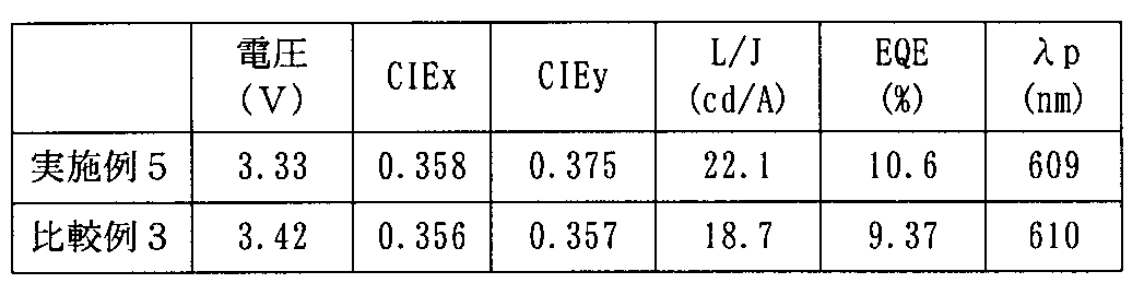
Table 2 shows the results of performance comparison of the elements of Example 5 and Comparative Example 3 at a current density of 1 mA / cm 2 .
膜厚130nmのITOが成膜されたITO基板上に、HI1、HT1、RH:RD(共蒸着)、HT1、BH1:BD2(共蒸着)、BH1:GD(共蒸着)、TB1、ET1を順次蒸着し、下記の構成からなる素子を得た。括弧内は膜厚(単位:nm)を示す。
ITO(130)/HI1(50)/HT1(35)/RH:RD(5;1%)/HT1(5)/BH1:BD2(25;7.5%)/BH1:GD(20:5wt%)/TB1(5)/ET1(20)/LiF(1)/Al(80) Example 6
HI1, HT1, RH: RD (co-evaporation), HT1, BH1: BD2 (co-evaporation), BH1: GD (co-evaporation), TB1, and ET1 are sequentially formed on an ITO substrate on which ITO having a thickness of 130 nm is formed. Evaporation was performed to obtain an element having the following configuration. The parentheses indicate the film thickness (unit: nm).
ITO (130) / HI1 (50) / HT1 (35) / RH: RD (5; 1%) / HT1 (5) / BH1: BD2 (25; 7.5%) / BH1: GD (20: 5 wt%) ) / TB1 (5) / ET1 (20) / LiF (1) / Al (80)
TB1を成膜しなかったこと以外は実施例6と同様にして順次成膜し、下記の構成からなる素子を得た。
ITO(130)/HI1(50)/HT1(35)/RH:RD(5:1wt%)/HT1(5)/BH1:BD2(25;7.5%)/BH1:GD(20;5%)/ET1(25)/LiF(1)/Al(80) Comparative Example 4
Except that TB1 was not formed, films were formed in the same manner as in Example 6 to obtain an element having the following configuration.
ITO (130) / HI1 (50) / HT1 (35) / RH: RD (5: 1 wt%) / HT1 (5) / BH1: BD2 (25; 7.5%) / BH1: GD (20; 5% ) / ET1 (25) / LiF (1) / Al (80)
実施例6と比較例4の素子について、電流密度1mA/cm2における性能比較を行った結果を表3に示す。
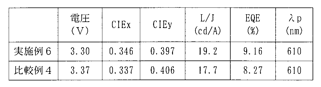
Table 3 shows the results of performance comparison of the elements of Example 6 and Comparative Example 4 at a current density of 1 mA / cm 2 .
実施例6と比較例4の外部量子効率を比較すると実施例6の方が1%程度高い値となっている。 In Example 6, a light-emitting layer in which a blue light-emitting layer and a green light-emitting layer are stacked is provided adjacent to an electron transport zone composed of a barrier layer TB1 and an electron injection layer ET1. Further, a red light emitting layer made of RH: RD is stacked via a charge barrier layer made of HT1. Thus, in Example 6, since three light emitting layers of blue, green, and red are laminated, white light emission is exhibited. In Comparative Example 4, the barrier layer TB1 is not used.
When the external quantum efficiencies of Example 6 and Comparative Example 4 are compared, Example 6 is about 1% higher.
実施例1と同様にして、下記の構成からなる素子を得た。括弧内は膜厚(単位:nm)を示す。
ITO(130)/HI2(50)/HT3(45)/BH2:BD3(25;5%)/TB1(5)/ET1(20)/LiF(1)/Al(80) Example 7
In the same manner as in Example 1, an element having the following configuration was obtained. The parentheses indicate the film thickness (unit: nm).
ITO (130) / HI2 (50) / HT3 (45) / BH2: BD3 (25; 5%) / TB1 (5) / ET1 (20) / LiF (1) / Al (80)
実施例1と同様にして、下記の構成からなる素子を得た。
ITO(130)/HI2(50)/HT3(45)/BH2:BD3(25;5%)/TB1(5)/ET2(20)/LiF(1)/Al(80) Example 8
In the same manner as in Example 1, an element having the following configuration was obtained.
ITO (130) / HI2 (50) / HT3 (45) / BH2: BD3 (25; 5%) / TB1 (5) / ET2 (20) / LiF (1) / Al (80)
実施例1と同様にして、下記の構成からなる素子を得た。
ITO(130)/HI2(50)/HT4(45)/BH3:BD3(25;5%)/TB1(5)/ET2(20)/LiF(1)/Al(80) Example 9
In the same manner as in Example 1, an element having the following configuration was obtained.
ITO (130) / HI2 (50) / HT4 (45) / BH3: BD3 (25; 5%) / TB1 (5) / ET2 (20) / LiF (1) / Al (80)
実施例1と同様にして、下記の構成からなる素子を得た。
ITO(130)/HI2(50)/HT3(45)/BH3:BD3(25;5%)/TB2(5)/ET2(20)/LiF(1)/Al(80) Example 10
In the same manner as in Example 1, an element having the following configuration was obtained.
ITO (130) / HI2 (50) / HT3 (45) / BH3: BD3 (25; 5%) / TB2 (5) / ET2 (20) / LiF (1) / Al (80)
実施例1と同様にして、下記の構成からなる素子を得た。
ITO(130)/HI2(50)/HT3(45)/BH2:BD3(25,5%)/TB2(5)/ET4(20)/LiF(1)/Al(80) Example 11
In the same manner as in Example 1, an element having the following configuration was obtained.
ITO (130) / HI2 (50) / HT3 (45) / BH2: BD3 (25,5%) / TB2 (5) / ET4 (20) / LiF (1) / Al (80)
実施例1と同様にして、下記の構成からなる素子を得た。
ITO(130)/HI2(50)/HT4(45)/BH3:BD3(25;5%)/TB2(5)/ET2(20)/LiF(1)/Al(80) Example 12
In the same manner as in Example 1, an element having the following configuration was obtained.
ITO (130) / HI2 (50) / HT4 (45) / BH3: BD3 (25; 5%) / TB2 (5) / ET2 (20) / LiF (1) / Al (80)
実施例1と同様にして、下記の構成からなる素子を得た。
ITO(130)/HI2(50)/HT4(45)/BH3:BD3(25;5%)/TB2(5)/ET3(20)/LiF(1)/Al(80) Example 13
In the same manner as in Example 1, an element having the following configuration was obtained.
ITO (130) / HI2 (50) / HT4 (45) / BH3: BD3 (25; 5%) / TB2 (5) / ET3 (20) / LiF (1) / Al (80)
実施例1と同様にして、下記の構成からなる素子を得た。
ITO(130)/HI2(50)/HT3(45)/BH3:BD3(25;5%)/TB3(5)/ET2(20)/LiF(1)/Al(80) Example 14
In the same manner as in Example 1, an element having the following configuration was obtained.
ITO (130) / HI2 (50) / HT3 (45) / BH3: BD3 (25; 5%) / TB3 (5) / ET2 (20) / LiF (1) / Al (80)
実施例1と同様にして、下記の構成からなる素子を得た。
ITO(130)/HI2(50)/HT4(45)/BH3:BD3(25;5%)/TB3(5)/ET2(20)/LiF(1)/Al(80) Example 15
In the same manner as in Example 1, an element having the following configuration was obtained.
ITO (130) / HI2 (50) / HT4 (45) / BH3: BD3 (25; 5%) / TB3 (5) / ET2 (20) / LiF (1) / Al (80)
実施例1と同様にして、下記の構成からなる素子を得た。
ITO(130)/HI2(50)/HT4(45)/BH3:BD3(25;5%)/TB4(5)/ET2(20)/LiF(1)/Al(80) Example 16
In the same manner as in Example 1, an element having the following configuration was obtained.
ITO (130) / HI2 (50) / HT4 (45) / BH3: BD3 (25; 5%) / TB4 (5) / ET2 (20) / LiF (1) / Al (80)
実施例1と同様にして、下記の構成からなる素子を得た。
ITO(130)/HI2(50)/HT4(45)/BH3:BD3(25;5%)/TB5(5)/ET2(20)/LiF(1)/Al(80) Example 17
In the same manner as in Example 1, an element having the following configuration was obtained.
ITO (130) / HI2 (50) / HT4 (45) / BH3: BD3 (25; 5%) / TB5 (5) / ET2 (20) / LiF (1) / Al (80)
実施例1と同様にして、下記の構成からなる素子を得た。
ITO(130)/HI2(50)/HT4(45)/BH3:BD3(25;5%)/TB6(5)/ET2(20)/LiF(1)/Al(80) Example 18
In the same manner as in Example 1, an element having the following configuration was obtained.
ITO (130) / HI2 (50) / HT4 (45) / BH3: BD3 (25; 5%) / TB6 (5) / ET2 (20) / LiF (1) / Al (80)
実施例1と同様にして、下記の構成からなる素子を得た。
ITO(130)/HI2(50)/HT4(45)/BH3:BD3(25;5%)/TB5(5)/ET3(20)/LiF(1)/Al(80) Example 19
In the same manner as in Example 1, an element having the following configuration was obtained.
ITO (130) / HI2 (50) / HT4 (45) / BH3: BD3 (25; 5%) / TB5 (5) / ET3 (20) / LiF (1) / Al (80)
実施例1と同様にして、下記の構成からなる素子を得た。
ITO(130)/HI2(50)/HT4(45)/BH3:BD3(25;5%)/TB6(5)/ET3(20)/LiF(1)/Al(80) Example 20
In the same manner as in Example 1, an element having the following configuration was obtained.
ITO (130) / HI2 (50) / HT4 (45) / BH3: BD3 (25; 5%) / TB6 (5) / ET3 (20) / LiF (1) / Al (80)
実施例7~20の素子について、実施例1と同様に電流密度10mA/cm2における性能評価を行った結果を表4に示す。
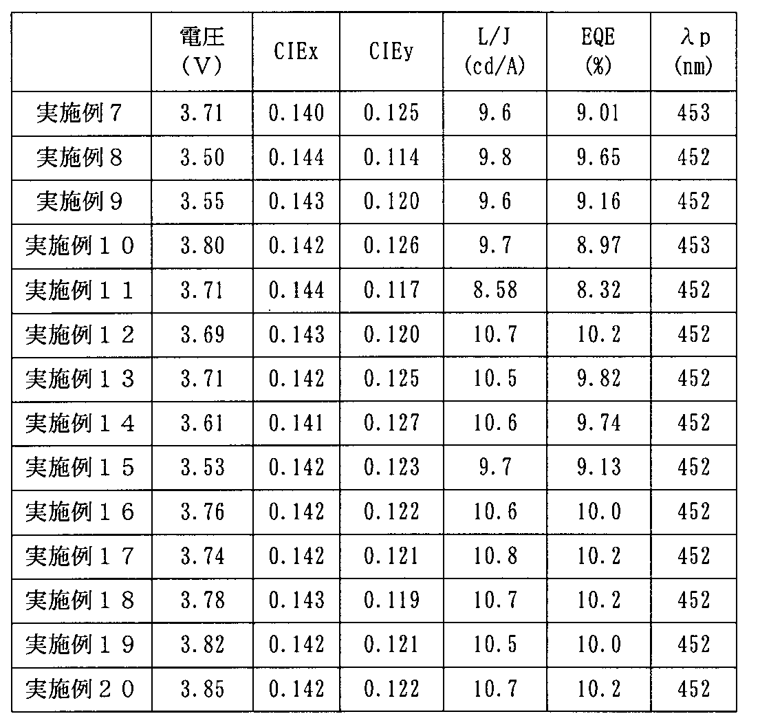
更に実施例8ではET1からより電子注入性の高いET2に代えることで0.21Vの低電圧化し、9.65%の高いEQEを示した。
実施例9では実施例7に対しHT4、BH3、ET2に変えても0.16V低電圧化し、9.16%のEQEを示した。
実施例10でTB1からTB2に変えることで若干の高電圧化を伴うものの、8.97%のEQEを示した。
実施例11で実施例10に対しET2をET4に代えても高い8.32%のEQEを示した。
実施例12で実施例10に対しHT3をHT4に変えることで0.11Vの低電圧化と共にEQEが10.2%にまで向上した。これは正孔注入量が増大したためである。
実施例13で実施例12に対しET2に代えてET3を用いた場合も、若干の高電圧化を伴うものの、高い効率を示した。
実施例14では実施例10に対しTB2に代えてTB3を用いた場合、0.19V低電圧化し9.74%のEQEを示した。
実施例15から18において、HT4とともにTB3,TB4,TB5,TB6のいずれを用いた場合でも高効率を示すことがわかる。
実施例19、20において、TB5,TB6とET3の組み合わせの場合でも高効率を示した。 Evaluation Example 4
Table 4 shows the results of performance evaluation of the elements of Examples 7 to 20 at a current density of 10 mA / cm 2 in the same manner as in Example 1.
Further, in Example 8, the voltage was lowered to 0.21 V by replacing ET1 with ET2 having higher electron injection property, and a high EQE of 9.65% was exhibited.
In Example 9, even when changed to HT4, BH3, and ET2 with respect to Example 7, the voltage was reduced by 0.16 V and showed an EQE of 9.16%.
In Example 10, changing from TB1 to TB2 resulted in a slight increase in voltage, but showed an EQE of 8.97%.
In Example 11, even when ET2 was replaced with ET4 compared to Example 10, a high 8.32% EQE was exhibited.
By changing HT3 from HT3 to HT4 in Example 12, the EQE was improved to 10.2% as the voltage decreased to 0.11V. This is because the hole injection amount has increased.
In Example 13, when ET3 was used in place of ET2 with respect to Example 12, high efficiency was exhibited although there was a slight increase in voltage.
In Example 14, when TB3 was used instead of TB2 with respect to Example 10, the voltage was reduced by 0.19 V and showed an EQE of 9.74%.
In Examples 15 to 18, it can be seen that high efficiency is exhibited when any of TB3, TB4, TB5, and TB6 is used together with HT4.
In Examples 19 and 20, high efficiency was exhibited even in the case of a combination of TB5, TB6 and ET3.
実施例1と同様にして、下記の構成からなる素子を得た。括弧内は膜厚(単位:nm)を示す。
ITO(130)/HI2(50)/HT5(45)/BH2:BD3(25;5%)/TB2(5)/ET2(20)/LiF(0.5)/Al(80) Example 21
In the same manner as in Example 1, an element having the following configuration was obtained. The parentheses indicate the film thickness (unit: nm).
ITO (130) / HI2 (50) / HT5 (45) / BH2: BD3 (25; 5%) / TB2 (5) / ET2 (20) / LiF (0.5) / Al (80)
実施例1と同様にして、下記の構成からなる素子を得た。
ITO(130)/HI2(50)/HT6(45)/BH2:BD3(25;5%)/TB2(5)/ET2(20)/LiF(0.5)/Al(80) Example 22
In the same manner as in Example 1, an element having the following configuration was obtained.
ITO (130) / HI2 (50) / HT6 (45) / BH2: BD3 (25; 5%) / TB2 (5) / ET2 (20) / LiF (0.5) / Al (80)
実施例1と同様にして、下記の構成からなる素子を得た。
ITO(130)/HI2(50)/HT7(45)/BH2:BD3(25;5%)/TB2(5)/ET2(20)/LiF(0.5)/Al(80) Example 23
In the same manner as in Example 1, an element having the following configuration was obtained.
ITO (130) / HI2 (50) / HT7 (45) / BH2: BD3 (25; 5%) / TB2 (5) / ET2 (20) / LiF (0.5) / Al (80)
実施例1と同様にして、下記の構成からなる素子を得た。
ITO(130)/HI2(50)/HT8(45)/BH2:BD3(25;5%)/TB2(5)/ET2(20)/LiF(0.5)/Al(80) Example 24
In the same manner as in Example 1, an element having the following configuration was obtained.
ITO (130) / HI2 (50) / HT8 (45) / BH2: BD3 (25; 5%) / TB2 (5) / ET2 (20) / LiF (0.5) / Al (80)
実施例1と同様にして、下記の構成からなる素子を得た。
ITO(130)/HI2(50)/HT9(45)/BH2:BD3(25;5%)/TB2(5)/ET2(20)/LiF(0.5)/Al(80) Example 25
In the same manner as in Example 1, an element having the following configuration was obtained.
ITO (130) / HI2 (50) / HT9 (45) / BH2: BD3 (25; 5%) / TB2 (5) / ET2 (20) / LiF (0.5) / Al (80)
実施例1と同様にして、下記の構成からなる素子を得た。
ITO(130)/HI2(50)/HT10(45)/BH2:BD3(25;5%)/TB2(5)/ET2(20)/LiF(0.5)/Al(80) Example 26
In the same manner as in Example 1, an element having the following configuration was obtained.
ITO (130) / HI2 (50) / HT10 (45) / BH2: BD3 (25; 5%) / TB2 (5) / ET2 (20) / LiF (0.5) / Al (80)
実施例21~26の素子について、実施例1と同様に電流密度10mA/cm2における性能評価を行った結果を表5に示す。
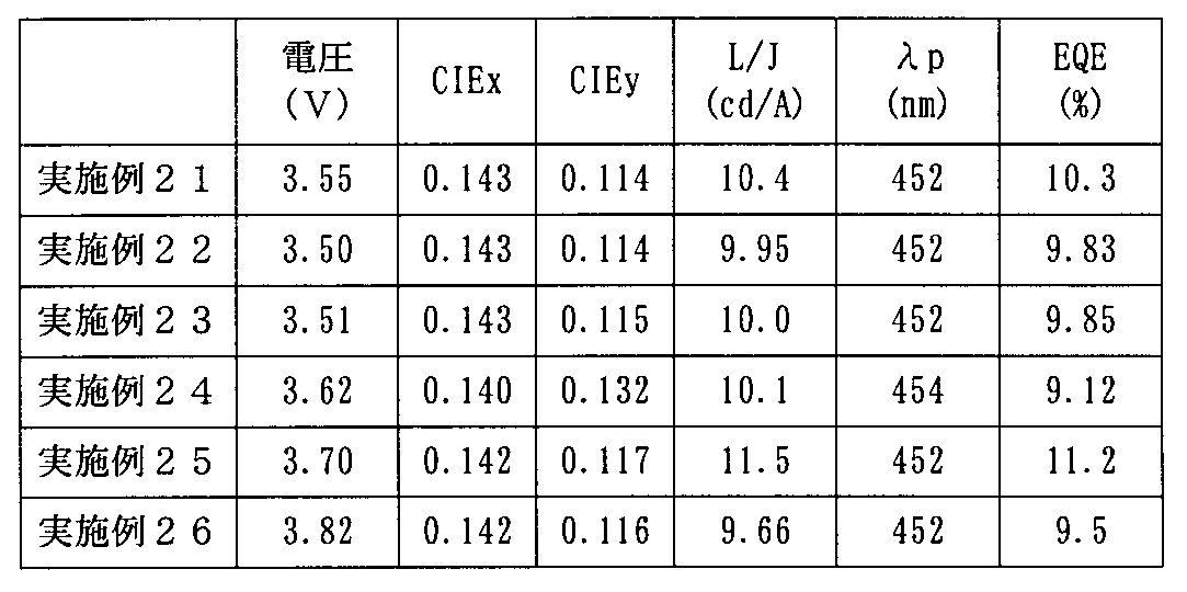
Table 5 shows the results of performance evaluation of the elements of Examples 21 to 26 at a current density of 10 mA / cm 2 in the same manner as in Example 1.
実施例1と同様にして、下記の構成からなる素子を得た。括弧内は膜厚(単位:nm)を示す。
ITO(130)/HI2(50)/HT4(45)/BH2:BD3(25;1.25%)/TB2(5)/ET2(20)/LiF(1)/Al(80) Example 27
In the same manner as in Example 1, an element having the following configuration was obtained. The parentheses indicate the film thickness (unit: nm).
ITO (130) / HI2 (50) / HT4 (45) / BH2: BD3 (25; 1.25%) / TB2 (5) / ET2 (20) / LiF (1) / Al (80)
実施例1と同様にして、下記の構成からなる素子を得た。
ITO(130)/HI2(50)/HT4(45)/BH3:BD4(25;1.25%)/TB2(5)/ET2(20)/LiF(1)/Al(80) Example 28
In the same manner as in Example 1, an element having the following configuration was obtained.
ITO (130) / HI2 (50) / HT4 (45) / BH3: BD4 (25; 1.25%) / TB2 (5) / ET2 (20) / LiF (1) / Al (80)
実施例27、28の素子について、実施例1と同様に電流密度10mA/cm2における性能評価を行った結果を表6に示す。

実施例28において、BD3に代えてBD4をドーパントとして用いた場合、電圧が3.91Vと高電圧化した。これはBD4のAfが3.45eVと大きく、電子トラップ性が大きいためである。一方、EQEは9.32%、TTF比率33.0%という高い値を示し、BD4を用いた場合でもTTFによる効率の向上効果が確認された。 Evaluation Example 6
Table 6 shows the results of performance evaluation of the elements of Examples 27 and 28 at a current density of 10 mA / cm 2 in the same manner as in Example 1.
In Example 28, when BD4 was used as a dopant instead of BD3, the voltage was increased to 3.91 V. This is because Af of BD4 is as large as 3.45 eV and the electron trapping property is large. On the other hand, EQE showed a high value of 9.32% and a TTF ratio of 33.0%, and even when BD4 was used, the effect of improving the efficiency by TTF was confirmed.
実施例1と同様にして、下記を順次積層した構成からなる素子を得た。括弧内は膜厚(単位:nm)を示す。
陽極 ITO(130)
正孔注入層 HI2(70)
正孔輸送層 HT4(10)/HT11(10)
赤緑発光層 PBH:PGD:PRD(50;10%,0.3%)
正孔障壁層 PGH(10)
電子輸送層 ET1(10)/ET3(5)
中間層 Li2O(0.1)/HAT(20)
正孔注入層 HI2(50)
正孔輸送層 HT3(45)
青発光層 BH2:BD3(25;5%)
障壁層 TB2(5)
電子輸送層 ET2(25)
電子注入層 LiF(1)
電極 Al(80) Example 29
In the same manner as in Example 1, an element having a structure in which the following was sequentially laminated was obtained. The parentheses indicate the film thickness (unit: nm).
Anode ITO (130)
Hole injection layer HI2 (70)
Hole transport layer HT4 (10) / HT11 (10)
Red-green light emitting layer PBH: PGD: PRD (50; 10%, 0.3%)
Hole barrier layer PGH (10)
Electron transport layer ET1 (10) / ET3 (5)
Intermediate layer Li 2 O (0.1) / HAT (20)
Hole injection layer HI2 (50)
Hole transport layer HT3 (45)
Blue light emitting layer BH2: BD3 (25; 5%)
Barrier layer TB2 (5)
Electron transport layer ET2 (25)
Electron injection layer LiF (1)
Electrode Al (80)
TB2を成膜しなかったこと以外は実施例29と同様にして順次成膜し、下記の構成からなる素子を得た。
陽極 ITO(130)
正孔注入層 HI2(70)
正孔輸送層 HT4(10)/HT11(10)
赤緑発光層 PBH:PGD:PRD(50;10%,0.3%)
正孔障壁層 PGH(10)
電子輸送層 ET1(10)/ET3(5)
中間層 Li2O(0.1)/HAT(20)
正孔注入層 HI2(50)
正孔輸送層 HT3(45)
青発光層 BH2:BD3(25;5%)
電子輸送層 ET2(25)
電子注入層 LiF(1)
電極 Al(80) Comparative Example 5
Except that TB2 was not formed, films were sequentially formed in the same manner as in Example 29 to obtain an element having the following configuration.
Anode ITO (130)
Hole injection layer HI2 (70)
Hole transport layer HT4 (10) / HT11 (10)
Red-green light emitting layer PBH: PGD: PRD (50; 10%, 0.3%)
Hole barrier layer PGH (10)
Electron transport layer ET1 (10) / ET3 (5)
Intermediate layer Li 2 O (0.1) / HAT (20)
Hole injection layer HI2 (50)
Hole transport layer HT3 (45)
Blue light emitting layer BH2: BD3 (25; 5%)
Electron transport layer ET2 (25)
Electron injection layer LiF (1)
Electrode Al (80)
実施例29、比較例5の素子について、実施例1と同様に電流密度10mA/cm2における性能評価を行った結果を表7に示す。
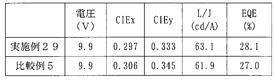
Table 7 shows the results of performance evaluation of the elements of Example 29 and Comparative Example 5 at a current density of 10 mA / cm 2 in the same manner as in Example 1.
Claims (15)
- 少なくとも陽極と、発光層と、電子輸送帯域と、陰極とをこの順に備え、
前記発光層は、ホストと、主ピーク波長が550nm以下の蛍光発光を示すドーパントとを含み、
前記ドーパントのアフィニティAdが前記ホストのアフィニティAh以上であり、
前記ドーパントの3重項エネルギーET dが前記ホストの3重項エネルギーET hより大きく、
前記電子輸送帯域内に、前記発光層に隣接して障壁層が設けられ、前記障壁層の3重項エネルギーET bがET hより大きい、
有機エレクトロルミネッセンス素子。 At least an anode, a light emitting layer, an electron transport zone, and a cathode are provided in this order,
The light emitting layer includes a host and a dopant exhibiting fluorescence emission having a main peak wavelength of 550 nm or less,
The dopant affinity Ad is greater than or equal to the host affinity Ah;
A triplet energy E T d of the dopant is greater than a triplet energy E T h of the host;
In the electron transport zone, a barrier layer is provided adjacent to the light emitting layer, and the triplet energy E T b of the barrier layer is greater than E T h .
Organic electroluminescence device. - 前記ドーパントがフルオランテン誘導体、ホウ素錯体から選択される化合物である請求項1に記載の有機エレクトロルミネッセンス素子。 The organic electroluminescence device according to claim 1, wherein the dopant is a compound selected from a fluoranthene derivative and a boron complex.
- 前記陽極と発光層の間に正孔輸送帯域を備え、
前記正孔輸送帯域内に、前記発光層に隣接して正孔輸送層が設けられ、前記正孔輸送層の3重項エネルギーET hoがET hより大きい、
請求項1又は2に記載の有機エレクトロルミネッセンス素子。 A hole transport zone is provided between the anode and the light emitting layer,
Wherein the hole transport in the band, the hole-transporting layer is provided adjacent to the light-emitting layer, the triplet energy E T ho of the hole-transporting layer is larger than E T h,
The organic electroluminescent element according to claim 1 or 2. - 前記障壁層が炭化水素芳香族化合物からなる請求項1~3のいずれかに記載の有機エレクトロルミネッセンス素子。 4. The organic electroluminescence device according to claim 1, wherein the barrier layer is made of a hydrocarbon aromatic compound.
- 前記炭化水素芳香族化合物が多環芳香族化合物である請求項4に記載の有機エレクトロルミネッセンス素子。 The organic electroluminescence device according to claim 4, wherein the hydrocarbon aromatic compound is a polycyclic aromatic compound.
- 前記障壁層を構成する材料の電子移動度が、電界強度0.04~0.5MV/cmの範囲において、10-6cm2/Vs以上である請求項1~5のいずれかに記載の有機エレクトロルミネッセンス素子。 6. The organic material according to claim 1, wherein the electron mobility of the material constituting the barrier layer is 10 −6 cm 2 / Vs or more in the range of electric field strength of 0.04 to 0.5 MV / cm. Electroluminescence element.
- 前記電子輸送帯域が前記障壁層及び電子注入層の積層体からなり、
前記電子注入層を構成する材料の電子移動度が、電界強度0.04~0.5MV/cmの範囲において、10-6cm2/Vs以上である請求項1~6のいずれかに記載の有機エレクトロルミネッセンス素子。 The electron transport zone comprises a laminate of the barrier layer and the electron injection layer;
7. The electron mobility of the material constituting the electron injection layer is 10 −6 cm 2 / Vs or more in the range of electric field strength of 0.04 to 0.5 MV / cm. Organic electroluminescence device. - 前記電子輸送帯域が前記障壁層及び電子注入層の積層体からなり、前記障壁層のアフィニティAb、前記電子注入層のアフィニティAeがAe-Ab<0.2eVで表わされる関係を満たす請求項1~6のいずれかに記載の有機エレクトロルミネッセンス素子。 The electron transport zone comprises a laminate of the barrier layer and the electron injection layer, and the affinity Ab of the barrier layer and the affinity Ae of the electron injection layer satisfy a relationship represented by Ae-Ab <0.2 eV. 6. The organic electroluminescence device according to any one of 6 above.
- 前記電子輸送帯域が前記障壁層1層で構成される請求項1~6のいずれかに記載の有機エレクトロルミネッセンス素子。 The organic electroluminescence device according to any one of claims 1 to 6, wherein the electron transport zone is composed of one barrier layer.
- 前記電子輸送帯域が前記障壁層1層で構成され、前記障壁層にドナーがドープされたものである請求項1~6のいずれかに記載の有機エレクトロルミネッセンス素子。 The organic electroluminescence device according to any one of claims 1 to 6, wherein the electron transport zone is composed of one barrier layer, and the barrier layer is doped with a donor.
- 前記ホストが環式構造以外に二重結合を含まない化合物である請求項1~10のいずれかに記載の有機エレクトロルミネッセンス素子。 The organic electroluminescence device according to any one of claims 1 to 10, wherein the host is a compound containing no double bond other than a cyclic structure.
- 前記ドーパントが環式構造以外に二重結合を含まない化合物である請求項1~11のいずれかに記載の有機エレクトロルミネッセンス素子。 12. The organic electroluminescence device according to claim 1, wherein the dopant is a compound containing no double bond other than a cyclic structure.
- 陽極と、発光層と、電子輸送帯域と、陰極とをこの順に備え、
前記発光層は、ホストと、蛍光発光性ドーパントとを含み、前記ドーパントのアフィニティAdが前記ホストのアフィニティAh以上であり、
前記ドーパントの3重項エネルギーET dが前記ホストの3重項エネルギーET hより大きく、
前記電子輸送帯域内に、前記発光層に隣接して障壁層が設けられ、前記障壁層を構成する材料の3重項エネルギーET bがET hより大きく、
電流効率(単位:cd/A)が最大となる印加電圧において、前記発光層に生成する3重項励起子同士が衝突して生成する1重項励起子由来の発光強度が、全発光強度に対して30%以上である、
有機エレクトロルミネッセンス素子。 An anode, a light emitting layer, an electron transport zone, and a cathode are provided in this order,
The light emitting layer includes a host and a fluorescent light emitting dopant, and the affinity Ad of the dopant is not less than the affinity Ah of the host,
A triplet energy E T d of the dopant is greater than a triplet energy E T h of the host;
In the electron transport zone, a barrier layer is provided adjacent to the light emitting layer, and the triplet energy E T b of the material constituting the barrier layer is larger than E T h ,
At an applied voltage at which current efficiency (unit: cd / A) is maximized, the emission intensity derived from singlet excitons generated by collision of triplet excitons generated in the light-emitting layer becomes the total emission intensity. For 30% or more,
Organic electroluminescence device. - 前記陽極と前記陰極の間に少なくとも2つの発光層を有し、2つの発光層の間に中間層を備える請求項1~13のいずれかに記載の有機エレクトロルミネッセンス素子。 The organic electroluminescence device according to any one of claims 1 to 13, wherein at least two light emitting layers are provided between the anode and the cathode, and an intermediate layer is provided between the two light emitting layers.
- 前記陽極と前記陰極の間に複数の発光層を含み、第一の発光層と第二の発光層の間に電荷障壁層を備える請求項1~13のいずれかに記載の有機エレクトロルミネッセンス素子。 The organic electroluminescence device according to any one of claims 1 to 13, further comprising a plurality of light-emitting layers between the anode and the cathode, and a charge barrier layer between the first light-emitting layer and the second light-emitting layer.
Priority Applications (3)
| Application Number | Priority Date | Filing Date | Title |
|---|---|---|---|
| JP2011514344A JP5208270B2 (en) | 2009-05-22 | 2010-05-21 | Organic electroluminescence device |
| EP10777586.8A EP2434558B1 (en) | 2009-05-22 | 2010-05-21 | Organic electroluminescent element |
| CN2010800218340A CN102428588A (en) | 2009-05-22 | 2010-05-21 | Organic electroluminescent element |
Applications Claiming Priority (2)
| Application Number | Priority Date | Filing Date | Title |
|---|---|---|---|
| JP2009124759 | 2009-05-22 | ||
| JP2009-124759 | 2009-05-22 |
Publications (1)
| Publication Number | Publication Date |
|---|---|
| WO2010134350A1 true WO2010134350A1 (en) | 2010-11-25 |
Family
ID=43124135
Family Applications (1)
| Application Number | Title | Priority Date | Filing Date |
|---|---|---|---|
| PCT/JP2010/003431 WO2010134350A1 (en) | 2009-05-22 | 2010-05-21 | Organic electroluminescent element |
Country Status (7)
| Country | Link |
|---|---|
| US (1) | US20100295444A1 (en) |
| EP (1) | EP2434558B1 (en) |
| JP (1) | JP5208270B2 (en) |
| KR (1) | KR20120029397A (en) |
| CN (1) | CN102428588A (en) |
| TW (1) | TW201103968A (en) |
| WO (1) | WO2010134350A1 (en) |
Cited By (126)
| Publication number | Priority date | Publication date | Assignee | Title |
|---|---|---|---|---|
| JP2009016478A (en) * | 2007-07-03 | 2009-01-22 | Canon Inc | Organic light emitting element |
| WO2011086941A1 (en) * | 2010-01-15 | 2011-07-21 | 出光興産株式会社 | Organic electroluminescent element |
| WO2012070233A1 (en) * | 2010-11-22 | 2012-05-31 | Idemitsu Kosan Co.,Ltd. | Organic electroluminescence device |
| WO2012133188A1 (en) | 2011-03-25 | 2012-10-04 | 出光興産株式会社 | Organic electroluminescent element |
| JP2013062262A (en) * | 2013-01-10 | 2013-04-04 | Panasonic Corp | Organic electroluminescent device |
| WO2013050862A1 (en) | 2011-10-07 | 2013-04-11 | ユーディーシー アイルランド リミテッド | Organic electroluminescent element, light emitting material therefor, light emitting device, display device, and illumination device |
| WO2013051234A1 (en) * | 2011-10-04 | 2013-04-11 | ソニー株式会社 | Organic electroluminescent element |
| JP2013084620A (en) * | 2013-01-10 | 2013-05-09 | Panasonic Corp | Organic electroluminescent element |
| WO2013064881A2 (en) | 2011-11-02 | 2013-05-10 | ユーディーシー アイルランド リミテッド | Organic electroluminescent element, material for organic electroluminescent element and light emitting device, display device, and illumination device, each employing organic electroluminescent element |
| WO2013072740A2 (en) | 2011-11-15 | 2013-05-23 | ユーディーシー アイルランド リミテッド | Charge-transporting material, organic electroluminescent element, and light-emitting device, display device and illumination device characterised by using said element |
| WO2013077352A1 (en) * | 2011-11-22 | 2013-05-30 | 出光興産株式会社 | Aromatic heterocyclic derivative, material for organic electroluminescent element, and organic electroluminescent element |
| WO2013084881A1 (en) | 2011-12-05 | 2013-06-13 | 出光興産株式会社 | Material for organic electroluminescent element and organic electroluminescent element |
| WO2013108069A2 (en) | 2011-10-06 | 2013-07-25 | ユーディーシー アイルランド リミテッド | Organic electroluminescent element, compound and material for organic electroluminescent element, used in the same, and light emitting device, display device and illumination device, using the element |
| DE102013201846A1 (en) | 2012-02-06 | 2013-08-14 | Udc Ireland Limited | Organic electroluminescence element, useful in a light emitting device, comprises substrate, pair of electrodes comprising anode and cathode, and layer of organic layers comprising light-emitting layer, which is arranged between electrodes |
| WO2013118846A1 (en) | 2012-02-10 | 2013-08-15 | 出光興産株式会社 | Aromatic amine derivative, organic electroluminescent element and electronic device |
| WO2013180241A1 (en) | 2012-06-01 | 2013-12-05 | 出光興産株式会社 | Organic electroluminescence element and material for organic electroluminescence element |
| WO2014013947A1 (en) | 2012-07-20 | 2014-01-23 | 出光興産株式会社 | Organic electroluminescent element |
| KR20140095491A (en) | 2011-11-22 | 2014-08-01 | 이데미쓰 고산 가부시키가이샤 | Aromatic heterocyclic derivative, material for organic electroluminescent element, and organic electroluminescent element |
| JP2014150249A (en) * | 2013-01-10 | 2014-08-21 | Semiconductor Energy Lab Co Ltd | Light-emitting element, light-emitting device, electronic apparatus and luminaire |
| WO2014168386A1 (en) * | 2013-04-08 | 2014-10-16 | 주식회사 엘엠에스 | Novel compound, and light-emitting device and electronic device including same |
| WO2014178441A1 (en) * | 2013-04-30 | 2014-11-06 | Canon Kabushiki Kaisha | Organic light emitting device |
| US8883323B2 (en) | 2010-11-22 | 2014-11-11 | Idemitsu Kosan Co., Ltd. | Organic electroluminescence device |
| WO2014199637A1 (en) | 2013-06-11 | 2014-12-18 | 出光興産株式会社 | Material for organic electroluminescent elements, organic electroluminescent element using same, and electronic device |
| WO2015005440A1 (en) * | 2013-07-10 | 2015-01-15 | Jnc株式会社 | Material for light-emitting auxiliary layer comprising ring-fused fluorene compound or fluorene compound |
| WO2015053403A1 (en) | 2013-10-11 | 2015-04-16 | 出光興産株式会社 | Aromatic amine compound, organic electroluminescent element and electronic device |
| WO2015072520A1 (en) | 2013-11-13 | 2015-05-21 | 出光興産株式会社 | Compound, material for organic electroluminescent element, organic electroluminescent element, and electronic device |
| KR20150060976A (en) | 2012-10-03 | 2015-06-03 | 이데미쓰 고산 가부시키가이샤 | Organic electroluminescent element |
| JP2015109407A (en) * | 2013-05-16 | 2015-06-11 | 株式会社半導体エネルギー研究所 | Light-emitting element, light-emitting device, electronic apparatus, and illumination apparatus |
| US9324950B2 (en) | 2010-11-22 | 2016-04-26 | Idemitsu Kosan Co., Ltd. | Organic electroluminescence device |
| JP2016092417A (en) * | 2014-10-31 | 2016-05-23 | 株式会社半導体エネルギー研究所 | Benzo[a]anthracene compound, light-emitting element, display device, electronic device, and illuminating device |
| JP2017022369A (en) * | 2015-07-09 | 2017-01-26 | 株式会社Joled | Organic EL element |
| WO2017018326A1 (en) * | 2015-07-24 | 2017-02-02 | コニカミノルタ株式会社 | Organic electroluminescent element, display device, and illumination device |
| KR20170021300A (en) | 2014-07-31 | 2017-02-27 | 코니카 미놀타 가부시키가이샤 | Organic electroluminescent element display device lighting device -conjugated compound and light-emitting thin film |
| KR20170021294A (en) | 2014-07-31 | 2017-02-27 | 코니카 미놀타 가부시키가이샤 | Organic electroluminescent device, light-emitting thin film, display unit, and illumination unit |
| WO2017065295A1 (en) * | 2015-10-15 | 2017-04-20 | 出光興産株式会社 | Organic electroluminescent element and electronic device |
| US9647226B2 (en) | 2012-12-03 | 2017-05-09 | Idemitsu Kosan Co., Ltd. | Organic electroluminescent element |
| WO2017082169A1 (en) * | 2015-11-10 | 2017-05-18 | シャープ株式会社 | Light-emitting element and method for manufacturing same, and light emission method |
| KR20170059985A (en) | 2014-09-17 | 2017-05-31 | 신닛테츠 수미킨 가가쿠 가부시키가이샤 | Organic electroluminescent element |
| WO2017115589A1 (en) | 2015-12-28 | 2017-07-06 | 新日鉄住金化学株式会社 | Organic electroluminescence element |
| JP2017147450A (en) * | 2017-03-22 | 2017-08-24 | 出光興産株式会社 | Organic electroluminescent element |
| WO2017159152A1 (en) | 2016-03-15 | 2017-09-21 | 新日鉄住金化学株式会社 | Organic electroluminescent element |
| KR20170128517A (en) | 2015-05-08 | 2017-11-22 | 코니카 미놀타 가부시키가이샤 | π conjugated compound, organic electroluminescent device material, luminescent material, luminescent thin film, organic electroluminescent device, display device and lighting device |
| KR20170134841A (en) | 2016-05-26 | 2017-12-07 | 삼성디스플레이 주식회사 | Compound including nitrogen and organic electroluminescence device including the same |
| KR20170137262A (en) | 2016-06-02 | 2017-12-13 | 삼성디스플레이 주식회사 | Polycyclic compound and organic electroluminescence device including the same |
| WO2017221999A1 (en) | 2016-06-22 | 2017-12-28 | Idemitsu Kosan Co., Ltd. | Specifically substituted benzofuro- and benzothienoquinolines for organic light emitting diodes |
| KR20180014723A (en) | 2015-05-29 | 2018-02-09 | 신닛테츠 수미킨 가가쿠 가부시키가이샤 | Organic electroluminescent device |
| WO2018061446A1 (en) | 2016-09-30 | 2018-04-05 | 新日鉄住金化学株式会社 | Organic electroluminescent element |
| US9966539B2 (en) | 2012-08-31 | 2018-05-08 | Idemitsu Kosan Co., Ltd. | Organic electroluminescence device |
| WO2018116152A1 (en) | 2016-12-19 | 2018-06-28 | Idemitsu Kosan Co., Ltd. | Specifically substituted ladder type compounds for organic light emitting devices |
| WO2018124313A1 (en) | 2016-12-29 | 2018-07-05 | Idemitsu Kosan Co., Ltd. | Nitrogen-containing heterocyclic compounds for organic light emitting devices |
| JP2018121064A (en) * | 2013-04-30 | 2018-08-02 | キヤノン株式会社 | Organic light-emitting element |
| WO2018154501A1 (en) | 2017-02-24 | 2018-08-30 | Idemitsu Kosan Co., Ltd. | Specific ladder type compounds for organic light emitting devices |
| KR20180099713A (en) | 2015-12-28 | 2018-09-05 | 신닛테츠 수미킨 가가쿠 가부시키가이샤 | Organic electroluminescent device |
| JPWO2017099160A1 (en) * | 2015-12-08 | 2018-09-27 | 出光興産株式会社 | ORGANIC EL LIGHT EMITTING DEVICE AND ELECTRONIC DEVICE |
| WO2018173593A1 (en) | 2017-03-23 | 2018-09-27 | 新日鉄住金化学株式会社 | Organic electroluminescent element |
| WO2018198844A1 (en) | 2017-04-27 | 2018-11-01 | 新日鉄住金化学株式会社 | Organic electroluminescent element |
| KR20180122645A (en) | 2016-03-28 | 2018-11-13 | 닛테츠 케미컬 앤드 머티리얼 가부시키가이샤 | Organic electroluminescent device |
| JP2019024140A (en) * | 2014-05-13 | 2019-02-14 | 株式会社半導体エネルギー研究所 | Light emitting device |
| JP2019091906A (en) * | 2013-09-17 | 2019-06-13 | 株式会社Kyulux | Organic electroluminescent device |
| KR20190097009A (en) | 2016-12-27 | 2019-08-20 | 닛테츠 케미컬 앤드 머티리얼 가부시키가이샤 | Materials for organic electroluminescent devices and organic electroluminescent devices |
| WO2019171891A1 (en) | 2018-03-07 | 2019-09-12 | 日鉄ケミカル&マテリアル株式会社 | Organic electroluminescent element |
| KR20190132629A (en) | 2017-03-30 | 2019-11-28 | 닛테츠 케미컬 앤드 머티리얼 가부시키가이샤 | Materials for organic electroluminescent devices and organic electroluminescent devices |
| WO2020009039A1 (en) * | 2018-07-05 | 2020-01-09 | キヤノン株式会社 | Organic el element and display device, image pickup device, communication equipment, illumination device, lamp fitting, and mobile body using said organic el element |
| JP2020013781A (en) * | 2018-07-05 | 2020-01-23 | キヤノン株式会社 | Organic el element, and display device, imaging device, communication apparatus, lighting device, lighting fixture, and mobile body using organic el element |
| EP3617210A1 (en) | 2018-08-31 | 2020-03-04 | Idemitsu Kosan Co., Ltd. | Polycyclic compound, and an organic electroluminescence device comprising the polycyclic compound |
| JP2020098916A (en) * | 2016-05-27 | 2020-06-25 | エルジー・ケム・リミテッド | Organic light emitting element |
| US10937979B2 (en) | 2018-04-26 | 2021-03-02 | Canon Kabushiki Kaisha | Organic el element, and display device, imaging apparatus, lighting device, and movable body including the same |
| WO2021065772A1 (en) * | 2019-10-04 | 2021-04-08 | 出光興産株式会社 | Organic electroluminescent element and electronic appliance |
| WO2021065491A1 (en) | 2019-09-30 | 2021-04-08 | 日鉄ケミカル&マテリアル株式会社 | Organic electroluminescent element |
| WO2021065774A1 (en) * | 2019-10-04 | 2021-04-08 | 出光興産株式会社 | Organic electroluminescent element and electronic device |
| WO2021065775A1 (en) * | 2019-10-04 | 2021-04-08 | 出光興産株式会社 | Organic electroluminescent element and electronic device |
| WO2021065492A1 (en) | 2019-09-30 | 2021-04-08 | 日鉄ケミカル&マテリアル株式会社 | Organic electroluminescent element |
| WO2021065773A1 (en) * | 2019-10-04 | 2021-04-08 | 出光興産株式会社 | Organic electroluminescent element and electronic device |
| WO2021132733A1 (en) | 2019-12-23 | 2021-07-01 | Idemitsu Kosan Co., Ltd. | Polycyclic compound, material for an organic electroluminescence device and an organic electroluminescence device comprising the polycyclic compound |
| WO2021131766A1 (en) | 2019-12-25 | 2021-07-01 | 日鉄ケミカル&マテリアル株式会社 | Organic electroluminescent element |
| WO2021131755A1 (en) | 2019-12-27 | 2021-07-01 | 日鉄ケミカル&マテリアル株式会社 | Organic electroluminescent element and method for manufacturing same |
| WO2021162122A1 (en) | 2020-02-14 | 2021-08-19 | Idemitsu Kosan Co., Ltd. | Compound, material for an organic electroluminescence device and an organic electroluminescence device comprising the compound |
| JP2021122018A (en) * | 2015-02-24 | 2021-08-26 | 株式会社半導体エネルギー研究所 | Light-emitting element, display device, electronic apparatus, and illumination device |
| EP3882238A1 (en) | 2020-03-19 | 2021-09-22 | Idemitsu Kosan Co.,Ltd. | Compound, material for an organic electroluminescence device and an organic electroluminescence device comprising the compound |
| WO2021200251A1 (en) | 2020-03-31 | 2021-10-07 | 日鉄ケミカル&マテリアル株式会社 | Organic electroluminescent device |
| WO2021200243A1 (en) | 2020-03-31 | 2021-10-07 | 日鉄ケミカル&マテリアル株式会社 | Organic electroluminescent element |
| WO2021220837A1 (en) | 2020-04-30 | 2021-11-04 | 日鉄ケミカル&マテリアル株式会社 | Material for organic electroluminescent element, and organic electroluminescent element |
| WO2021220838A1 (en) | 2020-04-30 | 2021-11-04 | 日鉄ケミカル&マテリアル株式会社 | Organic electroluminescence element material and organic electroluminescence element |
| KR20210143850A (en) | 2019-03-29 | 2021-11-29 | 닛테츠 케미컬 앤드 머티리얼 가부시키가이샤 | organic electroluminescent device |
| KR20210144768A (en) | 2019-03-25 | 2021-11-30 | 닛테츠 케미컬 앤드 머티리얼 가부시키가이샤 | Melt mixture for organic electroluminescent device, and organic electroluminescent device |
| KR20210148231A (en) | 2019-03-29 | 2021-12-07 | 닛테츠 케미컬 앤드 머티리얼 가부시키가이샤 | Polymers for organic electroluminescent devices and organic electroluminescent devices |
| KR20220002368A (en) | 2019-04-25 | 2022-01-06 | 닛테츠 케미컬 앤드 머티리얼 가부시키가이샤 | organic electroluminescent device |
| KR20220004655A (en) | 2019-04-25 | 2022-01-11 | 닛테츠 케미컬 앤드 머티리얼 가부시키가이샤 | organic electroluminescent device |
| WO2022009883A1 (en) | 2020-07-08 | 2022-01-13 | 日鉄ケミカル&マテリアル株式会社 | Heat-activated delayed fluorescence material and organic electroluminescent element |
| WO2022045272A1 (en) | 2020-08-28 | 2022-03-03 | 日鉄ケミカル&マテリアル株式会社 | Organic electroluminescent element |
| EP3975280A1 (en) | 2020-09-29 | 2022-03-30 | NIPPON STEEL Chemical & Material Co., Ltd. | Composition for organic electroluminescent element and organic electroluminescent element |
| WO2022085776A1 (en) | 2020-10-23 | 2022-04-28 | 日鉄ケミカル&マテリアル株式会社 | Material for organic electroluminescent element and organic electroluminescent element |
| WO2022085777A1 (en) | 2020-10-23 | 2022-04-28 | 日鉄ケミカル&マテリアル株式会社 | Material for organic electroluminescent elements, and organic electroluminescent element |
| WO2022085590A1 (en) | 2020-10-20 | 2022-04-28 | 日鉄ケミカル&マテリアル株式会社 | Light-emitting material, and organic electroluminescent element |
| KR20220061138A (en) | 2019-09-13 | 2022-05-12 | 이데미쓰 고산 가부시키가이샤 | Organic electroluminescent devices and electronic devices |
| WO2022118867A1 (en) * | 2020-12-02 | 2022-06-09 | 出光興産株式会社 | Organic electroluminescent element and electronic device |
| WO2022124366A1 (en) | 2020-12-11 | 2022-06-16 | 日鉄ケミカル&マテリアル株式会社 | Organic electroluminescent element |
| WO2022124367A1 (en) | 2020-12-11 | 2022-06-16 | 日鉄ケミカル&マテリアル株式会社 | Material for organic electroluminescent element and organic electroluminescent element |
| WO2022124365A1 (en) | 2020-12-11 | 2022-06-16 | 日鉄ケミカル&マテリアル株式会社 | Organic electroluminescent device |
| WO2022131123A1 (en) | 2020-12-18 | 2022-06-23 | 日鉄ケミカル&マテリアル株式会社 | Organic electroluminescent element and method for manufacturing same |
| WO2022149493A1 (en) | 2021-01-08 | 2022-07-14 | 日鉄ケミカル&マテリアル株式会社 | Organic electroluminescent element and method for producing same |
| EP4043453A1 (en) | 2021-02-11 | 2022-08-17 | Idemitsu Kosan Co., Ltd. | Compound, material for an organic electroluminescence device and an organic electroluminescence device comprising the compound |
| EP4060756A1 (en) | 2021-03-19 | 2022-09-21 | Idemitsu Kosan Co., Ltd. | An organic electroluminescence device comprising an azine compound and a rare earth metal, rare earth metal compound, and/or rare earth metal complex and an electronic equipment comprising said organic electroluminescence device |
| EP4068404A1 (en) | 2021-03-31 | 2022-10-05 | Idemitsu Kosan Co., Ltd. | An organic electroluminescence device comprising a light emitting layer comprising three different compounds and an electronic equipment comprising said organic electroluminescence device |
| WO2022215580A1 (en) | 2021-04-08 | 2022-10-13 | 日鉄ケミカル&マテリアル株式会社 | Light-emitting material, and organic electroluminescent element |
| KR20220141780A (en) | 2020-02-14 | 2022-10-20 | 이데미쓰 고산 가부시키가이샤 | Organic electroluminescent devices and electronic devices |
| KR20220160581A (en) | 2020-03-31 | 2022-12-06 | 닛테츠 케미컬 앤드 머티리얼 가부시키가이샤 | organic electroluminescent device |
| KR20220160573A (en) | 2020-03-31 | 2022-12-06 | 닛테츠 케미컬 앤드 머티리얼 가부시키가이샤 | organic electroluminescent device |
| WO2022255243A1 (en) | 2021-05-31 | 2022-12-08 | 日鉄ケミカル&マテリアル株式会社 | Deuteride and organic electroluminescent element |
| WO2022255241A1 (en) | 2021-05-31 | 2022-12-08 | 日鉄ケミカル&マテリアル株式会社 | Deuteride and organic electroluminescent element |
| WO2022255242A1 (en) | 2021-05-31 | 2022-12-08 | 日鉄ケミカル&マテリアル株式会社 | Deuteride and organic electroluminescent element |
| US11527720B1 (en) | 2021-08-13 | 2022-12-13 | Idemitsu Kosan Co., Ltd. | Organic electroluminescence device, electronic device, and compound |
| EP4124619A1 (en) | 2021-07-29 | 2023-02-01 | Idemitsu Kosan Co., Ltd. | Compound, material for an organic electroluminescence device and an organic electroluminescence device comprising the compound |
| US11575087B1 (en) | 2020-12-25 | 2023-02-07 | Idemitsu Kosan Co., Ltd. | Organic electroluminescence device, light emitting device, organic electroluminescence display device and electronic device |
| US11581487B2 (en) | 2017-04-26 | 2023-02-14 | Oti Lumionics Inc. | Patterned conductive coating for surface of an opto-electronic device |
| KR20230027191A (en) | 2020-06-19 | 2023-02-27 | 이데미쓰 고산 가부시키가이샤 | Organic electroluminescent elements and electronic devices |
| EP4140994A1 (en) | 2021-08-26 | 2023-03-01 | Idemitsu Kosan Co., Ltd. | Compound, material for an organic electroluminescence device and an organic electroluminescence device comprising the compound |
| EP4199130A1 (en) | 2021-12-15 | 2023-06-21 | Idemitsu Kosan Co.,Ltd. | An organic electroluminescence device comprising a light emitting layer comprising three different compounds and an electronic equipment comprising said organic electroluminescence device |
| US11730012B2 (en) | 2019-03-07 | 2023-08-15 | Oti Lumionics Inc. | Materials for forming a nucleation-inhibiting coating and devices incorporating same |
| KR20230125260A (en) | 2020-12-25 | 2023-08-29 | 이데미쓰 고산 가부시키가이샤 | Organic electroluminescent elements and electronic devices |
| US11751415B2 (en) | 2018-02-02 | 2023-09-05 | Oti Lumionics Inc. | Materials for forming a nucleation-inhibiting coating and devices incorporating same |
| KR20230134557A (en) | 2021-01-21 | 2023-09-21 | 이데미쓰 고산 가부시키가이샤 | Organic electroluminescent devices and electronic devices |
| KR20240001701A (en) | 2021-04-26 | 2024-01-03 | 이데미쓰 고산 가부시키가이샤 | Organic electroluminescent devices, organic electroluminescent display devices and electronic devices |
| KR20240023022A (en) | 2021-06-18 | 2024-02-20 | 닛테츠 케미컬 앤드 머티리얼 가부시키가이샤 | Materials for organic electroluminescent devices and organic electroluminescent devices |
| US11917844B2 (en) | 2018-04-26 | 2024-02-27 | Canon Kabushiki Kaisha | Organic EL element, and display apparatus, illumination apparatus, and moving object including the same |
| KR20240037890A (en) | 2021-07-30 | 2024-03-22 | 닛테츠 케미컬 앤드 머티리얼 가부시키가이샤 | organic electroluminescent device |
Families Citing this family (16)
| Publication number | Priority date | Publication date | Assignee | Title |
|---|---|---|---|---|
| US8154195B2 (en) * | 2007-07-07 | 2012-04-10 | Idemitsu Kosan Co., Ltd. | Organic electroluminescence device and material for organic electroluminescence device |
| WO2011148909A1 (en) | 2010-05-24 | 2011-12-01 | 出光興産株式会社 | Organic electroluminescent element |
| US20140231774A1 (en) * | 2011-09-09 | 2014-08-21 | Lg Chem, Ltd. | Material for organic light-emitting device, and organic light-emitting device using same |
| US10600983B2 (en) | 2013-03-29 | 2020-03-24 | Kyulux, Inc. | Organic electroluminescent device comprising delayed fluorescent materials |
| KR20230054771A (en) | 2013-12-02 | 2023-04-25 | 가부시키가이샤 한도오따이 에네루기 켄큐쇼 | Light-emitting element, light-emitting device, electronic appliance, and lighting device |
| CN105633295A (en) * | 2014-11-06 | 2016-06-01 | 上海和辉光电有限公司 | Organic light-emitting diode fluorescent device structure and manufacture method thereof |
| CN106033793B (en) * | 2015-03-09 | 2018-11-13 | 广东阿格蕾雅光电材料有限公司 | Organic electroluminescence device |
| US9525134B1 (en) * | 2015-08-11 | 2016-12-20 | E I Du Pont De Nemours And Company | Hole transport materials |
| JP6854489B2 (en) * | 2016-03-23 | 2021-04-07 | コニカミノルタ株式会社 | Method for Producing Triaryl Borane and Its Intermediate |
| KR102389824B1 (en) | 2017-12-29 | 2022-04-25 | 경희대학교 산학협력단 | Organic light emitting device and display device having the same |
| WO2019229591A1 (en) | 2018-05-31 | 2019-12-05 | 株式会社半導体エネルギー研究所 | Organic compound, light emitting element, light emitting device, electronic apparatus, and lighting device |
| CN109411633B (en) * | 2018-08-31 | 2020-12-15 | 昆山国显光电有限公司 | Organic electroluminescent device, preparation method thereof and display device |
| TWI826522B (en) * | 2018-09-12 | 2023-12-21 | 德商麥克專利有限公司 | Electroluminescent devices |
| KR20200110578A (en) | 2019-03-15 | 2020-09-24 | 삼성디스플레이 주식회사 | Organic light emitting device and display apparatus comprising the same |
| KR20210059526A (en) | 2019-11-15 | 2021-05-25 | 엘지디스플레이 주식회사 | Organic Light Emitting Device and Display Device Using the Same |
| CN116134982A (en) * | 2020-08-19 | 2023-05-16 | 株式会社弗莱斯克 | Organic EL element |
Citations (34)
| Publication number | Priority date | Publication date | Assignee | Title |
|---|---|---|---|---|
| JPS6479297A (en) | 1987-09-22 | 1989-03-24 | Mitsubishi Heavy Ind Ltd | Apparatus for production of high-concentration coal-water slurry |
| JPH11345687A (en) | 1998-06-01 | 1999-12-14 | Canon Inc | Luminescent element |
| JP2001357972A (en) * | 2000-06-13 | 2001-12-26 | Hitachi Ltd | Organic electroluminescent element |
| WO2002014244A1 (en) | 2000-08-10 | 2002-02-21 | Mitsui Chemicals, Inc. | Hydrocarbon compound, material for organic electroluminescent element and organic electroluminescent element |
| JP2002100478A (en) | 2000-09-20 | 2002-04-05 | Mitsubishi Chemicals Corp | Organic electroluminescence element and its method of manufacture |
| JP2002525808A (en) | 1998-09-14 | 2002-08-13 | ザ、トラスティーズ オブ プリンストン ユニバーシティ | Structure for high efficiency electroluminescent devices |
| JP2003338377A (en) | 2002-03-11 | 2003-11-28 | Tdk Corp | Organic el element |
| WO2004044088A1 (en) | 2002-11-12 | 2004-05-27 | Idemitsu Kosan Co., Ltd. | Material for organic electroluminescent device and organic electroluminescent device using same |
| JP2004204238A (en) | 2002-12-24 | 2004-07-22 | Lg Electronics Inc | Organic electroluminescent device |
| JP2004214180A (en) | 2002-12-16 | 2004-07-29 | Canon Inc | Organic light-emitting element |
| WO2004083162A1 (en) | 2003-03-20 | 2004-09-30 | Idemitsu Kosan Co. Ltd. | Aromatic amine derivative and organic electroluminescent element made with the same |
| JP2005072012A (en) | 2003-08-27 | 2005-03-17 | Novaled Gmbh | Light emitting device and manufacturing method therefor |
| JP2005314239A (en) | 2004-04-27 | 2005-11-10 | Mitsui Chemicals Inc | Anthracene compound and organic electroluminescent element containing the anthracene compound |
| WO2005108348A1 (en) | 2004-05-12 | 2005-11-17 | Idemitsu Kosan Co., Ltd. | Aromatic amine derivative, organic electroluminescent element employing the same, and process for producing aromatic amine derivative |
| WO2005113531A1 (en) | 2004-05-21 | 2005-12-01 | Toray Industries, Inc. | Light-emitting device material and light-emitting device |
| JP2005353288A (en) * | 2004-06-08 | 2005-12-22 | Canon Inc | Organic light-emitting element |
| US7018723B2 (en) | 2003-07-25 | 2006-03-28 | The University Of Southern California | Materials and structures for enhancing the performance of organic light emitting devices |
| JP2006278035A (en) | 2005-03-28 | 2006-10-12 | Idemitsu Kosan Co Ltd | Light emission distribution estimation method, light emission distribution estimation device, light emission distribution estimation program, record medium, display device, and image display device |
| WO2007021117A1 (en) | 2005-08-16 | 2007-02-22 | Gracel Display Inc. | Green electroluminescent compounds and organic electroluminescent device using the same |
| JP2007059903A (en) * | 2005-08-25 | 2007-03-08 | Internatl Business Mach Corp <Ibm> | Electroluminescence device (enhancement in stability of optoelectronic device) |
| WO2007100010A1 (en) | 2006-02-28 | 2007-09-07 | Idemitsu Kosan Co., Ltd. | Organic electroluminescent device |
| US20070273270A1 (en) | 2006-05-25 | 2007-11-29 | Idemitsu Kosan Co., Ltd. | Organic electroluminescence device |
| KR20070115588A (en) | 2006-06-01 | 2007-12-06 | 에스에프씨 주식회사 | Blue light emitting compound and organic electroluminescent device using the same |
| WO2008023623A1 (en) | 2006-08-22 | 2008-02-28 | Idemitsu Kosan Co., Ltd. | Organic electroluminescent device |
| JP2008506798A (en) * | 2004-07-15 | 2008-03-06 | メルク パテント ゲーエムベーハー | Use of polymers for upconversion and devices for upconversion |
| US7358661B2 (en) | 2003-04-24 | 2008-04-15 | Idemitsu Kosan Co., Ltd. | Organic electroluminescent device and display |
| WO2008062773A1 (en) | 2006-11-20 | 2008-05-29 | Idemitsu Kosan Co., Ltd. | Organic electroluminescent device |
| JP4134280B2 (en) | 2006-05-25 | 2008-08-20 | 出光興産株式会社 | Organic electroluminescence device and full-color light emitting device |
| KR20080079956A (en) | 2007-02-28 | 2008-09-02 | 에스에프씨 주식회사 | Blue light emitting compound and organic electroluminescent device using the same |
| JP2008212102A (en) | 2007-03-07 | 2008-09-18 | Mitsubishi Agricult Mach Co Ltd | Combine |
| WO2008145239A2 (en) | 2007-05-29 | 2008-12-04 | Merck Patent Gmbh | Benzanthracene derivatives for organic electroluminescent devices |
| JP2009090379A (en) | 2007-10-03 | 2009-04-30 | Nakamura Tome Precision Ind Co Ltd | Hard brittle sheet chamfering device having dress apparatus |
| WO2009084512A1 (en) | 2007-12-28 | 2009-07-09 | Idemitsu Kosan Co., Ltd. | Aromatic amine derivative and organic electroluminescent device using the same |
| KR20100024894A (en) | 2008-08-26 | 2010-03-08 | 에스에프씨 주식회사 | Pyrene compound and organic electroluminescent device using the same |
Family Cites Families (4)
| Publication number | Priority date | Publication date | Assignee | Title |
|---|---|---|---|---|
| JPH1079297A (en) * | 1996-07-09 | 1998-03-24 | Sony Corp | Electroluminescent element |
| US6660411B2 (en) * | 2000-09-20 | 2003-12-09 | Mitsubishi Chemical Corporation | Organic electroluminescent device |
| US9070884B2 (en) * | 2005-04-13 | 2015-06-30 | Universal Display Corporation | Hybrid OLED having phosphorescent and fluorescent emitters |
| US20080286610A1 (en) * | 2007-05-17 | 2008-11-20 | Deaton Joseph C | Hybrid oled with fluorescent and phosphorescent layers |
-
2009
- 2009-06-03 US US12/477,599 patent/US20100295444A1/en not_active Abandoned
-
2010
- 2010-05-21 CN CN2010800218340A patent/CN102428588A/en active Pending
- 2010-05-21 KR KR1020117027664A patent/KR20120029397A/en not_active Application Discontinuation
- 2010-05-21 EP EP10777586.8A patent/EP2434558B1/en active Active
- 2010-05-21 JP JP2011514344A patent/JP5208270B2/en active Active
- 2010-05-21 WO PCT/JP2010/003431 patent/WO2010134350A1/en active Application Filing
- 2010-05-24 TW TW099116455A patent/TW201103968A/en unknown
Patent Citations (34)
| Publication number | Priority date | Publication date | Assignee | Title |
|---|---|---|---|---|
| JPS6479297A (en) | 1987-09-22 | 1989-03-24 | Mitsubishi Heavy Ind Ltd | Apparatus for production of high-concentration coal-water slurry |
| JPH11345687A (en) | 1998-06-01 | 1999-12-14 | Canon Inc | Luminescent element |
| JP2002525808A (en) | 1998-09-14 | 2002-08-13 | ザ、トラスティーズ オブ プリンストン ユニバーシティ | Structure for high efficiency electroluminescent devices |
| JP2001357972A (en) * | 2000-06-13 | 2001-12-26 | Hitachi Ltd | Organic electroluminescent element |
| WO2002014244A1 (en) | 2000-08-10 | 2002-02-21 | Mitsui Chemicals, Inc. | Hydrocarbon compound, material for organic electroluminescent element and organic electroluminescent element |
| JP2002100478A (en) | 2000-09-20 | 2002-04-05 | Mitsubishi Chemicals Corp | Organic electroluminescence element and its method of manufacture |
| JP2003338377A (en) | 2002-03-11 | 2003-11-28 | Tdk Corp | Organic el element |
| WO2004044088A1 (en) | 2002-11-12 | 2004-05-27 | Idemitsu Kosan Co., Ltd. | Material for organic electroluminescent device and organic electroluminescent device using same |
| JP2004214180A (en) | 2002-12-16 | 2004-07-29 | Canon Inc | Organic light-emitting element |
| JP2004204238A (en) | 2002-12-24 | 2004-07-22 | Lg Electronics Inc | Organic electroluminescent device |
| WO2004083162A1 (en) | 2003-03-20 | 2004-09-30 | Idemitsu Kosan Co. Ltd. | Aromatic amine derivative and organic electroluminescent element made with the same |
| US7358661B2 (en) | 2003-04-24 | 2008-04-15 | Idemitsu Kosan Co., Ltd. | Organic electroluminescent device and display |
| US7018723B2 (en) | 2003-07-25 | 2006-03-28 | The University Of Southern California | Materials and structures for enhancing the performance of organic light emitting devices |
| JP2005072012A (en) | 2003-08-27 | 2005-03-17 | Novaled Gmbh | Light emitting device and manufacturing method therefor |
| JP2005314239A (en) | 2004-04-27 | 2005-11-10 | Mitsui Chemicals Inc | Anthracene compound and organic electroluminescent element containing the anthracene compound |
| WO2005108348A1 (en) | 2004-05-12 | 2005-11-17 | Idemitsu Kosan Co., Ltd. | Aromatic amine derivative, organic electroluminescent element employing the same, and process for producing aromatic amine derivative |
| WO2005113531A1 (en) | 2004-05-21 | 2005-12-01 | Toray Industries, Inc. | Light-emitting device material and light-emitting device |
| JP2005353288A (en) * | 2004-06-08 | 2005-12-22 | Canon Inc | Organic light-emitting element |
| JP2008506798A (en) * | 2004-07-15 | 2008-03-06 | メルク パテント ゲーエムベーハー | Use of polymers for upconversion and devices for upconversion |
| JP2006278035A (en) | 2005-03-28 | 2006-10-12 | Idemitsu Kosan Co Ltd | Light emission distribution estimation method, light emission distribution estimation device, light emission distribution estimation program, record medium, display device, and image display device |
| WO2007021117A1 (en) | 2005-08-16 | 2007-02-22 | Gracel Display Inc. | Green electroluminescent compounds and organic electroluminescent device using the same |
| JP2007059903A (en) * | 2005-08-25 | 2007-03-08 | Internatl Business Mach Corp <Ibm> | Electroluminescence device (enhancement in stability of optoelectronic device) |
| WO2007100010A1 (en) | 2006-02-28 | 2007-09-07 | Idemitsu Kosan Co., Ltd. | Organic electroluminescent device |
| US20070273270A1 (en) | 2006-05-25 | 2007-11-29 | Idemitsu Kosan Co., Ltd. | Organic electroluminescence device |
| JP4134280B2 (en) | 2006-05-25 | 2008-08-20 | 出光興産株式会社 | Organic electroluminescence device and full-color light emitting device |
| KR20070115588A (en) | 2006-06-01 | 2007-12-06 | 에스에프씨 주식회사 | Blue light emitting compound and organic electroluminescent device using the same |
| WO2008023623A1 (en) | 2006-08-22 | 2008-02-28 | Idemitsu Kosan Co., Ltd. | Organic electroluminescent device |
| WO2008062773A1 (en) | 2006-11-20 | 2008-05-29 | Idemitsu Kosan Co., Ltd. | Organic electroluminescent device |
| KR20080079956A (en) | 2007-02-28 | 2008-09-02 | 에스에프씨 주식회사 | Blue light emitting compound and organic electroluminescent device using the same |
| JP2008212102A (en) | 2007-03-07 | 2008-09-18 | Mitsubishi Agricult Mach Co Ltd | Combine |
| WO2008145239A2 (en) | 2007-05-29 | 2008-12-04 | Merck Patent Gmbh | Benzanthracene derivatives for organic electroluminescent devices |
| JP2009090379A (en) | 2007-10-03 | 2009-04-30 | Nakamura Tome Precision Ind Co Ltd | Hard brittle sheet chamfering device having dress apparatus |
| WO2009084512A1 (en) | 2007-12-28 | 2009-07-09 | Idemitsu Kosan Co., Ltd. | Aromatic amine derivative and organic electroluminescent device using the same |
| KR20100024894A (en) | 2008-08-26 | 2010-03-08 | 에스에프씨 주식회사 | Pyrene compound and organic electroluminescent device using the same |
Non-Patent Citations (10)
| Title |
|---|
| BERNHARD NICKEL ET AL.: "DELAYED FLUORESCENCE FROM THE LOWEST1B+3mum STATE OF ANTHRACENE, DUE TO HETERO-TRIPLET-TRIPLET ANNIHILATION OF 3ANTHRACENE* AND 3XANTHONE*", CHEMICAL PHYSICS, 1982, pages 365 - 376, XP008149484 * |
| CHIMED GANZORIG ET AL.: "A possible mechanism for enhanced electrofluoresecence emission through triplet-triplet annihilation in organic electroluminescent devices", APPLIED PHYSICS LETTERS, vol. 81, no. 17, 21 October 2002 (2002-10-21), pages 3137 - 3139, XP012032244 * |
| CHIMED GANZORIG ET AL.: "Evidence for enhanced electrofluorescence emission through triplet-triplet annihilation in organic electroluminescent devices", DAI 49 KAI EXTENDED ABSTRACTS, JAPAN SOCIETY OF APPLIED PHYSICS AND RELATED SOCIETIES, March 2002 (2002-03-01), pages 1314 - 28A-YE-4, XP008166764 * |
| D.V.KONDAKOV ET AL.: "Triplet annihilation exceeding spin statistical limit in highly efficient fluorescent organic light-emitting diodes", JOURNAL OF APPLIED PHYSICS, vol. 106, 2009, pages 124510, XP012127460 * |
| D.Y.KONDAKOV: "Characterization of triplet-triplet annihilation in organic light-emitting diodes based on anthracene derivatives", JOURNAL OF APPLIED PHYSICS, vol. 102, 2007, pages 114504, XP012105139 * |
| JOURNAL OF APPLIED PHYSICS, vol. 102, 2007, pages 114504 |
| S.M. BACHILO ET AL., J. PHYS. CHEM. A, vol. 104, 2000, pages 7711 |
| See also references of EP2434558A4 |
| SHIZUO TOKITO ET AL.: "Yuki EL Device no Ko Koritsuka", THE CHEMICAL TIMES, no. 2, 2010, pages 5, XP008149511 * |
| SID 2008 DIGEST, 2008, pages 709 |
Cited By (240)
| Publication number | Priority date | Publication date | Assignee | Title |
|---|---|---|---|---|
| JP2009016478A (en) * | 2007-07-03 | 2009-01-22 | Canon Inc | Organic light emitting element |
| US8803420B2 (en) | 2010-01-15 | 2014-08-12 | Idemitsu Kosan Co., Ltd. | Organic electroluminescence device |
| WO2011086941A1 (en) * | 2010-01-15 | 2011-07-21 | 出光興産株式会社 | Organic electroluminescent element |
| JP5238889B2 (en) * | 2010-01-15 | 2013-07-17 | 出光興産株式会社 | Organic electroluminescence device |
| USRE47654E1 (en) | 2010-01-15 | 2019-10-22 | Idemitsu Koasn Co., Ltd. | Organic electroluminescence device |
| US8883323B2 (en) | 2010-11-22 | 2014-11-11 | Idemitsu Kosan Co., Ltd. | Organic electroluminescence device |
| US9324950B2 (en) | 2010-11-22 | 2016-04-26 | Idemitsu Kosan Co., Ltd. | Organic electroluminescence device |
| WO2012070234A1 (en) * | 2010-11-22 | 2012-05-31 | Idemitsu Kosan Co.,Ltd. | Organic electroluminescence device |
| WO2012070233A1 (en) * | 2010-11-22 | 2012-05-31 | Idemitsu Kosan Co.,Ltd. | Organic electroluminescence device |
| US8643268B2 (en) | 2011-03-25 | 2014-02-04 | Idemitsu Kosan Co., Ltd. | Organic electroluminescence device |
| US10879482B2 (en) | 2011-03-25 | 2020-12-29 | Idemitsu Kosan Co., Ltd. | Organic electroluminescence device |
| WO2012133188A1 (en) | 2011-03-25 | 2012-10-04 | 出光興産株式会社 | Organic electroluminescent element |
| KR20140015385A (en) | 2011-03-25 | 2014-02-06 | 이데미쓰 고산 가부시키가이샤 | Organic electroluminescent element |
| EP3598520A1 (en) | 2011-03-25 | 2020-01-22 | Idemitsu Kosan Co., Ltd | Organic electroluminescent element |
| KR20160101214A (en) | 2011-03-25 | 2016-08-24 | 이데미쓰 고산 가부시키가이샤 | Organic electroluminescent element |
| US10411212B2 (en) | 2011-10-04 | 2019-09-10 | Idemitsu Kosan Co., Ltd. | Organic electroluminescent element |
| WO2013051234A1 (en) * | 2011-10-04 | 2013-04-11 | ソニー株式会社 | Organic electroluminescent element |
| WO2013108069A2 (en) | 2011-10-06 | 2013-07-25 | ユーディーシー アイルランド リミテッド | Organic electroluminescent element, compound and material for organic electroluminescent element, used in the same, and light emitting device, display device and illumination device, using the element |
| WO2013050862A1 (en) | 2011-10-07 | 2013-04-11 | ユーディーシー アイルランド リミテッド | Organic electroluminescent element, light emitting material therefor, light emitting device, display device, and illumination device |
| WO2013064881A2 (en) | 2011-11-02 | 2013-05-10 | ユーディーシー アイルランド リミテッド | Organic electroluminescent element, material for organic electroluminescent element and light emitting device, display device, and illumination device, each employing organic electroluminescent element |
| WO2013072740A2 (en) | 2011-11-15 | 2013-05-23 | ユーディーシー アイルランド リミテッド | Charge-transporting material, organic electroluminescent element, and light-emitting device, display device and illumination device characterised by using said element |
| CN107342368B (en) * | 2011-11-22 | 2019-05-28 | 出光兴产株式会社 | Aromatic heterocyclic derivative, material for organic electroluminescent element, and organic electroluminescent element |
| US9209406B2 (en) | 2011-11-22 | 2015-12-08 | Idemitsu Kosan Co., Ltd. | Aromatic heterocyclic derivative, material for organic electroluminescent element, and organic electroluminescent element |
| CN107342368A (en) * | 2011-11-22 | 2017-11-10 | 出光兴产株式会社 | Aromatic heterocyclic derivative, material for organic electroluminescent element, and organic electroluminescent element |
| US9847501B2 (en) | 2011-11-22 | 2017-12-19 | Idemitsu Kosan Co., Ltd. | Aromatic heterocyclic derivative, material for organic electroluminescent element, and organic electroluminescent element |
| CN107501244A (en) * | 2011-11-22 | 2017-12-22 | 出光兴产株式会社 | Aromatic heterocyclic derivative, material for organic electroluminescent element, and organic electroluminescent element |
| WO2013077352A1 (en) * | 2011-11-22 | 2013-05-30 | 出光興産株式会社 | Aromatic heterocyclic derivative, material for organic electroluminescent element, and organic electroluminescent element |
| KR20180008922A (en) | 2011-11-22 | 2018-01-24 | 이데미쓰 고산 가부시키가이샤 | Aromatic heterocyclic derivative, material for organic electroluminescent element, and organic electroluminescent element |
| US9893296B2 (en) | 2011-11-22 | 2018-02-13 | Idemitsu Kosan Co., Ltd. | Aromatic heterocyclic derivative, material for organic electroluminescent element, and organic electroluminescent element |
| KR20140095491A (en) | 2011-11-22 | 2014-08-01 | 이데미쓰 고산 가부시키가이샤 | Aromatic heterocyclic derivative, material for organic electroluminescent element, and organic electroluminescent element |
| EP3211682A1 (en) | 2011-11-22 | 2017-08-30 | Idemitsu Kosan Co., Ltd | Aromatic heterocyclic derivative, organic electroluminescence device material and organic electroluminescence device field |
| US10418563B2 (en) | 2011-11-22 | 2019-09-17 | Idemitsu Kosan Co., Ltd. | Aromatic heterocyclic derivative, material for organic electroluminescent element, and organic electroluminescent element |
| JPWO2013077352A1 (en) * | 2011-11-22 | 2015-04-27 | 出光興産株式会社 | Aromatic heterocyclic derivative, material for organic electroluminescence device, and organic electroluminescence device |
| KR20180049266A (en) | 2011-11-22 | 2018-05-10 | 이데미쓰 고산 가부시키가이샤 | Aromatic heterocyclic derivative, material for organic electroluminescent element, and organic electroluminescent element |
| US11374176B2 (en) | 2011-11-22 | 2022-06-28 | Idemitsu Kosan Co., Ltd. | Aromatic heterocyclic derivative, material for organic electroluminescent element, and organic electroluminescent element |
| US10199580B2 (en) | 2011-11-22 | 2019-02-05 | Idemitsu Kosan Co., Ltd. | Aromatic heterocyclic derivative, material for organic electroluminescent element, and organic electroluminescent element |
| CN103380508A (en) * | 2011-11-22 | 2013-10-30 | 出光兴产株式会社 | Aromatic heterocyclic derivative, material for organic electroluminescent element, and organic electroluminescent element |
| WO2013084881A1 (en) | 2011-12-05 | 2013-06-13 | 出光興産株式会社 | Material for organic electroluminescent element and organic electroluminescent element |
| US9306171B2 (en) | 2011-12-05 | 2016-04-05 | Idemitsu Kosan Co., Ltd. | Material for organic electroluminescence device and organic electroluminescence device |
| DE102013201846B4 (en) | 2012-02-06 | 2021-09-09 | Udc Ireland Limited | Organic electroluminescent element, compound for organic electroluminescent element that can be used here, light-emitting device, display device, and lighting device each using the element |
| DE102013201846A1 (en) | 2012-02-06 | 2013-08-14 | Udc Ireland Limited | Organic electroluminescence element, useful in a light emitting device, comprises substrate, pair of electrodes comprising anode and cathode, and layer of organic layers comprising light-emitting layer, which is arranged between electrodes |
| WO2013118846A1 (en) | 2012-02-10 | 2013-08-15 | 出光興産株式会社 | Aromatic amine derivative, organic electroluminescent element and electronic device |
| US9871203B2 (en) | 2012-02-10 | 2018-01-16 | Idemitsu Kosan Co., Ltd. | Aromatic amine derivative, organic electroluminescent element and electronic device |
| EP3809482A2 (en) | 2012-06-01 | 2021-04-21 | Idemitsu Kosan Co.,Ltd. | Organic electroluminescence element and material for organic electroluminescence element |
| US9099658B2 (en) | 2012-06-01 | 2015-08-04 | Idemitsu Kosan Co., Ltd. | Organic electroluminescence device |
| WO2013180241A1 (en) | 2012-06-01 | 2013-12-05 | 出光興産株式会社 | Organic electroluminescence element and material for organic electroluminescence element |
| USRE49343E1 (en) | 2012-06-01 | 2022-12-20 | Idemitsu Kosan Co., Ltd. | Organic electroluminescence device |
| US10032998B2 (en) | 2012-07-20 | 2018-07-24 | Idemitsu Kosan Co., Ltd. | Organic electroluminescent element |
| US10461264B2 (en) | 2012-07-20 | 2019-10-29 | Idemitsu Kosan Co., Ltd. | Organic electroluminescent element |
| US9608209B2 (en) | 2012-07-20 | 2017-03-28 | Idemitsu Kosan Co., Ltd. | Organic electroluminescent element |
| US9219242B2 (en) | 2012-07-20 | 2015-12-22 | Idemitsu Kosan Co., Ltd. | Organic electroluminescent element |
| US10930860B2 (en) | 2012-07-20 | 2021-02-23 | Idemitsu Kosan Co., Ltd. | Organic electroluminescent element |
| EP3249711A1 (en) | 2012-07-20 | 2017-11-29 | Idemitsu Kosan Co., Ltd. | Organic electroluminescent element |
| WO2014013947A1 (en) | 2012-07-20 | 2014-01-23 | 出光興産株式会社 | Organic electroluminescent element |
| US9966539B2 (en) | 2012-08-31 | 2018-05-08 | Idemitsu Kosan Co., Ltd. | Organic electroluminescence device |
| US9899620B2 (en) | 2012-10-03 | 2018-02-20 | Idemitsu Kosan Co. Ltd. | Organic electroluminescent element |
| KR20150060976A (en) | 2012-10-03 | 2015-06-03 | 이데미쓰 고산 가부시키가이샤 | Organic electroluminescent element |
| US9614170B2 (en) | 2012-10-03 | 2017-04-04 | Idemitsu Kosan Co., Ltd. | Organic electroluminescent element |
| KR20190131613A (en) | 2012-10-03 | 2019-11-26 | 이데미쓰 고산 가부시키가이샤 | Organic electroluminescent element |
| US9647226B2 (en) | 2012-12-03 | 2017-05-09 | Idemitsu Kosan Co., Ltd. | Organic electroluminescent element |
| JP2013084620A (en) * | 2013-01-10 | 2013-05-09 | Panasonic Corp | Organic electroluminescent element |
| JP2013062262A (en) * | 2013-01-10 | 2013-04-04 | Panasonic Corp | Organic electroluminescent device |
| JP2014150249A (en) * | 2013-01-10 | 2014-08-21 | Semiconductor Energy Lab Co Ltd | Light-emitting element, light-emitting device, electronic apparatus and luminaire |
| US9935286B2 (en) | 2013-01-10 | 2018-04-03 | Semiconductor Energy Laboratory Co., Ltd. | Light-emitting element, light-emitting device, electronic device, and lighting device |
| WO2014168386A1 (en) * | 2013-04-08 | 2014-10-16 | 주식회사 엘엠에스 | Novel compound, and light-emitting device and electronic device including same |
| US10141534B2 (en) | 2013-04-08 | 2018-11-27 | LMS Co.,Ltd. | Compound, and light-emitting device and electronic device including same |
| WO2014178441A1 (en) * | 2013-04-30 | 2014-11-06 | Canon Kabushiki Kaisha | Organic light emitting device |
| JP2014232861A (en) * | 2013-04-30 | 2014-12-11 | キヤノン株式会社 | Organic light-emitting element |
| US10854821B2 (en) | 2013-04-30 | 2020-12-01 | Canon Kabushiki Kaisha | Organic light emitting device |
| JP2018121064A (en) * | 2013-04-30 | 2018-08-02 | キヤノン株式会社 | Organic light-emitting element |
| JP2015109407A (en) * | 2013-05-16 | 2015-06-11 | 株式会社半導体エネルギー研究所 | Light-emitting element, light-emitting device, electronic apparatus, and illumination apparatus |
| KR20160008570A (en) * | 2013-05-16 | 2016-01-22 | 가부시키가이샤 한도오따이 에네루기 켄큐쇼 | Light-emitting element, light-emitting device, electronic device, and lighting device |
| JP2019216288A (en) * | 2013-05-16 | 2019-12-19 | 株式会社半導体エネルギー研究所 | Light emitting element |
| JP2021121041A (en) * | 2013-05-16 | 2021-08-19 | 株式会社半導体エネルギー研究所 | Light emitting element |
| KR102198634B1 (en) | 2013-05-16 | 2021-01-06 | 가부시키가이샤 한도오따이 에네루기 켄큐쇼 | Light-emitting element, light-emitting device, electronic device, and lighting device |
| US10128455B2 (en) | 2013-05-16 | 2018-11-13 | Semiconductor Energy Laboratory Co., Ltd. | Light-emitting element, light-emitting device, electronic device, and lighting device |
| JP7232868B2 (en) | 2013-05-16 | 2023-03-03 | 株式会社半導体エネルギー研究所 | light emitting element |
| US11462701B2 (en) | 2013-05-16 | 2022-10-04 | Semiconductor Energy Laboratory Co., Ltd. | Light-emitting element, light-emitting device, electronic device, and lighting device |
| WO2014199637A1 (en) | 2013-06-11 | 2014-12-18 | 出光興産株式会社 | Material for organic electroluminescent elements, organic electroluminescent element using same, and electronic device |
| WO2015005440A1 (en) * | 2013-07-10 | 2015-01-15 | Jnc株式会社 | Material for light-emitting auxiliary layer comprising ring-fused fluorene compound or fluorene compound |
| JPWO2015005440A1 (en) * | 2013-07-10 | 2017-03-02 | Jnc株式会社 | Material for light emitting auxiliary layer containing ring condensed fluorene compound or fluorene compound |
| JP2019091906A (en) * | 2013-09-17 | 2019-06-13 | 株式会社Kyulux | Organic electroluminescent device |
| EP4345089A2 (en) | 2013-10-11 | 2024-04-03 | Idemitsu Kosan Co.,Ltd. | Aromatic amine compound, organic electroluminescent element and electronic device |
| WO2015053403A1 (en) | 2013-10-11 | 2015-04-16 | 出光興産株式会社 | Aromatic amine compound, organic electroluminescent element and electronic device |
| WO2015072520A1 (en) | 2013-11-13 | 2015-05-21 | 出光興産株式会社 | Compound, material for organic electroluminescent element, organic electroluminescent element, and electronic device |
| US10217954B2 (en) | 2013-11-13 | 2019-02-26 | Idemitsu Kosan Co., Ltd. | Compound, material for organic electroluminescent element, organic electroluminescent element, and electronic device |
| JP2019024140A (en) * | 2014-05-13 | 2019-02-14 | 株式会社半導体エネルギー研究所 | Light emitting device |
| US11158832B2 (en) | 2014-05-13 | 2021-10-26 | Semiconductor Energy Laboratory Co., Ltd. | Light-emitting device with exciplex light-emitting layers |
| US10686153B2 (en) | 2014-05-13 | 2020-06-16 | Semiconductor Energy Laboratory Co., Ltd. | Exciplex light-emitting device |
| US11864403B2 (en) | 2014-05-13 | 2024-01-02 | Semiconductor Energy Laboratory Co., Ltd. | Light-emitting device comprising first to third light-emitting layers |
| US10950799B2 (en) | 2014-07-31 | 2021-03-16 | Merck Patent Gmbh | Organic electroluminescent element, display device, lighting device, PI-conjugated compound, and light-emitting thin film |
| KR20190115112A (en) | 2014-07-31 | 2019-10-10 | 코니카 미놀타 가부시키가이샤 | Organic electroluminescent device, light-emitting thin film, display unit, and illumination unit |
| KR20170021300A (en) | 2014-07-31 | 2017-02-27 | 코니카 미놀타 가부시키가이샤 | Organic electroluminescent element display device lighting device -conjugated compound and light-emitting thin film |
| US11329234B2 (en) | 2014-07-31 | 2022-05-10 | Merck Patent Gmbh | Organic electroluminescent element, display device, lighting device, π-conjugated compound, and light-emitting thin film |
| KR20170021294A (en) | 2014-07-31 | 2017-02-27 | 코니카 미놀타 가부시키가이샤 | Organic electroluminescent device, light-emitting thin film, display unit, and illumination unit |
| US10862048B2 (en) | 2014-07-31 | 2020-12-08 | Merck Patent Gmbh | Organic electroluminescent device, thin luminous film, display apparatus, and lighting apparatus |
| KR20170059985A (en) | 2014-09-17 | 2017-05-31 | 신닛테츠 수미킨 가가쿠 가부시키가이샤 | Organic electroluminescent element |
| US10862041B2 (en) | 2014-10-31 | 2020-12-08 | Semiconductor Energy Laboratory Co., Ltd. | Benzo[a]anthracene compound, light-emitting element, display device, electronic device, and lighting device |
| US11851594B2 (en) | 2014-10-31 | 2023-12-26 | Semiconductor Energy Laboratory Co., Ltd. | Benzo[a]anthracene compound, light-emitting element, display device, electronic device, and lighting device |
| JP2016092417A (en) * | 2014-10-31 | 2016-05-23 | 株式会社半導体エネルギー研究所 | Benzo[a]anthracene compound, light-emitting element, display device, electronic device, and illuminating device |
| US11563177B2 (en) | 2014-10-31 | 2023-01-24 | Semiconductor Energy Laboratory Co., Ltd. | Benzo[a]anthracene compound, light-emitting element, display device, electronic device, and lighting device |
| JP2021061417A (en) * | 2014-10-31 | 2021-04-15 | 株式会社半導体エネルギー研究所 | Light-emitting element, display device, electronic apparatus, and illumination device |
| JP7411765B2 (en) | 2014-10-31 | 2024-01-11 | 株式会社半導体エネルギー研究所 | Light emitting elements, display devices, electronic devices and lighting devices |
| JP2021122018A (en) * | 2015-02-24 | 2021-08-26 | 株式会社半導体エネルギー研究所 | Light-emitting element, display device, electronic apparatus, and illumination device |
| JP7179117B2 (en) | 2015-02-24 | 2022-11-28 | 株式会社半導体エネルギー研究所 | Light-emitting elements, display devices, electronic devices and lighting devices |
| US11358951B2 (en) | 2015-05-08 | 2022-06-14 | Merck Patent Gmbh | Π(PI)-conjugated compound, organic electroluminescence element material, light-emitting material, light-emitting thin film, organic electroluminescence element, display device, and illumination device |
| KR20170128517A (en) | 2015-05-08 | 2017-11-22 | 코니카 미놀타 가부시키가이샤 | π conjugated compound, organic electroluminescent device material, luminescent material, luminescent thin film, organic electroluminescent device, display device and lighting device |
| KR20180014723A (en) | 2015-05-29 | 2018-02-09 | 신닛테츠 수미킨 가가쿠 가부시키가이샤 | Organic electroluminescent device |
| JP2017022369A (en) * | 2015-07-09 | 2017-01-26 | 株式会社Joled | Organic EL element |
| US10651395B2 (en) | 2015-07-24 | 2020-05-12 | Konica Minolta, Inc. | Organic electroluminescent element, display device, and illumination device |
| CN107925006B (en) * | 2015-07-24 | 2020-09-01 | 柯尼卡美能达株式会社 | Organic electroluminescent element, display device, and lighting device |
| KR20180010223A (en) | 2015-07-24 | 2018-01-30 | 코니카 미놀타 가부시키가이샤 | Organic electroluminescence device, display device and lighting device |
| CN107925006A (en) * | 2015-07-24 | 2018-04-17 | 柯尼卡美能达株式会社 | Organic electroluminescent device, display device and lighting device |
| WO2017018326A1 (en) * | 2015-07-24 | 2017-02-02 | コニカミノルタ株式会社 | Organic electroluminescent element, display device, and illumination device |
| JPWO2017018326A1 (en) * | 2015-07-24 | 2018-05-24 | コニカミノルタ株式会社 | Organic electroluminescence element, display device and lighting device |
| WO2017065295A1 (en) * | 2015-10-15 | 2017-04-20 | 出光興産株式会社 | Organic electroluminescent element and electronic device |
| JPWO2017082169A1 (en) * | 2015-11-10 | 2018-08-09 | シャープ株式会社 | Light emitting device and light emitting method |
| WO2017082169A1 (en) * | 2015-11-10 | 2017-05-18 | シャープ株式会社 | Light-emitting element and method for manufacturing same, and light emission method |
| JPWO2017099160A1 (en) * | 2015-12-08 | 2018-09-27 | 出光興産株式会社 | ORGANIC EL LIGHT EMITTING DEVICE AND ELECTRONIC DEVICE |
| US11322711B2 (en) | 2015-12-08 | 2022-05-03 | Idemitsu Kosan Co., Ltd. | Organic EL light emitting apparatus and electronic instrument |
| JP2021009859A (en) * | 2015-12-08 | 2021-01-28 | 出光興産株式会社 | Organic el light-emitting device and electronic apparatus |
| US10854838B2 (en) | 2015-12-08 | 2020-12-01 | Idemitsu Kosan Co., Ltd. | Organic EL light emitting apparatus and electronic instrument |
| JP7017933B2 (en) | 2015-12-08 | 2022-02-09 | 出光興産株式会社 | Organic EL light emitting device and electronic device |
| KR20180099713A (en) | 2015-12-28 | 2018-09-05 | 신닛테츠 수미킨 가가쿠 가부시키가이샤 | Organic electroluminescent device |
| WO2017115589A1 (en) | 2015-12-28 | 2017-07-06 | 新日鉄住金化学株式会社 | Organic electroluminescence element |
| KR20180099669A (en) | 2015-12-28 | 2018-09-05 | 신닛테츠 수미킨 가가쿠 가부시키가이샤 | Organic electroluminescent device |
| US11088334B2 (en) | 2016-03-15 | 2021-08-10 | Nippon Steel Chemical & Material Co., Ltd. | Organic electroluminescent element |
| WO2017159152A1 (en) | 2016-03-15 | 2017-09-21 | 新日鉄住金化学株式会社 | Organic electroluminescent element |
| KR20180122645A (en) | 2016-03-28 | 2018-11-13 | 닛테츠 케미컬 앤드 머티리얼 가부시키가이샤 | Organic electroluminescent device |
| KR20170134841A (en) | 2016-05-26 | 2017-12-07 | 삼성디스플레이 주식회사 | Compound including nitrogen and organic electroluminescence device including the same |
| JP2020098916A (en) * | 2016-05-27 | 2020-06-25 | エルジー・ケム・リミテッド | Organic light emitting element |
| US10714693B2 (en) | 2016-06-02 | 2020-07-14 | Samsung Display Co., Ltd. | Polycyclic compound and organic electroluminescence device including the same |
| KR20170137262A (en) | 2016-06-02 | 2017-12-13 | 삼성디스플레이 주식회사 | Polycyclic compound and organic electroluminescence device including the same |
| WO2017221999A1 (en) | 2016-06-22 | 2017-12-28 | Idemitsu Kosan Co., Ltd. | Specifically substituted benzofuro- and benzothienoquinolines for organic light emitting diodes |
| KR20190055122A (en) | 2016-09-30 | 2019-05-22 | 닛테츠 케미컬 앤드 머티리얼 가부시키가이샤 | Organic electroluminescent device |
| WO2018061446A1 (en) | 2016-09-30 | 2018-04-05 | 新日鉄住金化学株式会社 | Organic electroluminescent element |
| WO2018116152A1 (en) | 2016-12-19 | 2018-06-28 | Idemitsu Kosan Co., Ltd. | Specifically substituted ladder type compounds for organic light emitting devices |
| KR20230024436A (en) | 2016-12-27 | 2023-02-20 | 닛테츠 케미컬 앤드 머티리얼 가부시키가이샤 | Material for organic electroluminescent element, and organic electroluminescent element |
| KR20190097009A (en) | 2016-12-27 | 2019-08-20 | 닛테츠 케미컬 앤드 머티리얼 가부시키가이샤 | Materials for organic electroluminescent devices and organic electroluminescent devices |
| WO2018124313A1 (en) | 2016-12-29 | 2018-07-05 | Idemitsu Kosan Co., Ltd. | Nitrogen-containing heterocyclic compounds for organic light emitting devices |
| WO2018154501A1 (en) | 2017-02-24 | 2018-08-30 | Idemitsu Kosan Co., Ltd. | Specific ladder type compounds for organic light emitting devices |
| JP2017147450A (en) * | 2017-03-22 | 2017-08-24 | 出光興産株式会社 | Organic electroluminescent element |
| WO2018173593A1 (en) | 2017-03-23 | 2018-09-27 | 新日鉄住金化学株式会社 | Organic electroluminescent element |
| US11374178B2 (en) | 2017-03-23 | 2022-06-28 | Nippon Steel Chemical & Material Co., Ltd. | Organic electroluminescent element |
| KR20190128208A (en) | 2017-03-23 | 2019-11-15 | 닛테츠 케미컬 앤드 머티리얼 가부시키가이샤 | Organic electroluminescent element |
| KR20190132629A (en) | 2017-03-30 | 2019-11-28 | 닛테츠 케미컬 앤드 머티리얼 가부시키가이샤 | Materials for organic electroluminescent devices and organic electroluminescent devices |
| US11581487B2 (en) | 2017-04-26 | 2023-02-14 | Oti Lumionics Inc. | Patterned conductive coating for surface of an opto-electronic device |
| KR20230151560A (en) | 2017-04-27 | 2023-11-01 | 닛테츠 케미컬 앤드 머티리얼 가부시키가이샤 | Organic electroluminescent element |
| KR20200002885A (en) | 2017-04-27 | 2020-01-08 | 닛테츠 케미컬 앤드 머티리얼 가부시키가이샤 | Organic electroluminescent element |
| WO2018198844A1 (en) | 2017-04-27 | 2018-11-01 | 新日鉄住金化学株式会社 | Organic electroluminescent element |
| US11751415B2 (en) | 2018-02-02 | 2023-09-05 | Oti Lumionics Inc. | Materials for forming a nucleation-inhibiting coating and devices incorporating same |
| WO2019171891A1 (en) | 2018-03-07 | 2019-09-12 | 日鉄ケミカル&マテリアル株式会社 | Organic electroluminescent element |
| KR20200129097A (en) | 2018-03-07 | 2020-11-17 | 닛테츠 케미컬 앤드 머티리얼 가부시키가이샤 | Organic electroluminescent device |
| US10937979B2 (en) | 2018-04-26 | 2021-03-02 | Canon Kabushiki Kaisha | Organic el element, and display device, imaging apparatus, lighting device, and movable body including the same |
| US11917844B2 (en) | 2018-04-26 | 2024-02-27 | Canon Kabushiki Kaisha | Organic EL element, and display apparatus, illumination apparatus, and moving object including the same |
| WO2020009039A1 (en) * | 2018-07-05 | 2020-01-09 | キヤノン株式会社 | Organic el element and display device, image pickup device, communication equipment, illumination device, lamp fitting, and mobile body using said organic el element |
| JP2020013781A (en) * | 2018-07-05 | 2020-01-23 | キヤノン株式会社 | Organic el element, and display device, imaging device, communication apparatus, lighting device, lighting fixture, and mobile body using organic el element |
| JP7336277B2 (en) | 2018-07-05 | 2023-08-31 | キヤノン株式会社 | Organic EL elements and display devices using the same, imaging devices, communication devices, lighting devices, lamps, mobile objects |
| WO2020044270A1 (en) | 2018-08-31 | 2020-03-05 | Idemitsu Kosan Co., Ltd. | Polycyclic compound, and an organic electroluminescence device comprising the polycyclic compound |
| EP3617210A1 (en) | 2018-08-31 | 2020-03-04 | Idemitsu Kosan Co., Ltd. | Polycyclic compound, and an organic electroluminescence device comprising the polycyclic compound |
| US11730012B2 (en) | 2019-03-07 | 2023-08-15 | Oti Lumionics Inc. | Materials for forming a nucleation-inhibiting coating and devices incorporating same |
| KR20210144768A (en) | 2019-03-25 | 2021-11-30 | 닛테츠 케미컬 앤드 머티리얼 가부시키가이샤 | Melt mixture for organic electroluminescent device, and organic electroluminescent device |
| KR20210148231A (en) | 2019-03-29 | 2021-12-07 | 닛테츠 케미컬 앤드 머티리얼 가부시키가이샤 | Polymers for organic electroluminescent devices and organic electroluminescent devices |
| KR20210143850A (en) | 2019-03-29 | 2021-11-29 | 닛테츠 케미컬 앤드 머티리얼 가부시키가이샤 | organic electroluminescent device |
| KR20220004655A (en) | 2019-04-25 | 2022-01-11 | 닛테츠 케미컬 앤드 머티리얼 가부시키가이샤 | organic electroluminescent device |
| KR20220002368A (en) | 2019-04-25 | 2022-01-06 | 닛테츠 케미컬 앤드 머티리얼 가부시키가이샤 | organic electroluminescent device |
| KR20220061138A (en) | 2019-09-13 | 2022-05-12 | 이데미쓰 고산 가부시키가이샤 | Organic electroluminescent devices and electronic devices |
| WO2021065492A1 (en) | 2019-09-30 | 2021-04-08 | 日鉄ケミカル&マテリアル株式会社 | Organic electroluminescent element |
| WO2021065491A1 (en) | 2019-09-30 | 2021-04-08 | 日鉄ケミカル&マテリアル株式会社 | Organic electroluminescent element |
| KR20220071204A (en) | 2019-09-30 | 2022-05-31 | 닛테츠 케미컬 앤드 머티리얼 가부시키가이샤 | organic electroluminescent device |
| KR20220075332A (en) | 2019-09-30 | 2022-06-08 | 닛테츠 케미컬 앤드 머티리얼 가부시키가이샤 | organic electroluminescent device |
| WO2021065772A1 (en) * | 2019-10-04 | 2021-04-08 | 出光興産株式会社 | Organic electroluminescent element and electronic appliance |
| WO2021065773A1 (en) * | 2019-10-04 | 2021-04-08 | 出光興産株式会社 | Organic electroluminescent element and electronic device |
| WO2021065775A1 (en) * | 2019-10-04 | 2021-04-08 | 出光興産株式会社 | Organic electroluminescent element and electronic device |
| WO2021065774A1 (en) * | 2019-10-04 | 2021-04-08 | 出光興産株式会社 | Organic electroluminescent element and electronic device |
| WO2021132733A1 (en) | 2019-12-23 | 2021-07-01 | Idemitsu Kosan Co., Ltd. | Polycyclic compound, material for an organic electroluminescence device and an organic electroluminescence device comprising the polycyclic compound |
| WO2021131766A1 (en) | 2019-12-25 | 2021-07-01 | 日鉄ケミカル&マテリアル株式会社 | Organic electroluminescent element |
| KR20220117207A (en) | 2019-12-25 | 2022-08-23 | 닛테츠 케미컬 앤드 머티리얼 가부시키가이샤 | organic electroluminescent device |
| KR20220119370A (en) | 2019-12-27 | 2022-08-29 | 닛테츠 케미컬 앤드 머티리얼 가부시키가이샤 | Organic electroluminescent device and its manufacturing method |
| WO2021131755A1 (en) | 2019-12-27 | 2021-07-01 | 日鉄ケミカル&マテリアル株式会社 | Organic electroluminescent element and method for manufacturing same |
| KR20220141780A (en) | 2020-02-14 | 2022-10-20 | 이데미쓰 고산 가부시키가이샤 | Organic electroluminescent devices and electronic devices |
| US11552259B1 (en) | 2020-02-14 | 2023-01-10 | Idemitsu Kosan Co., Ltd. | Organic electroluminescent element and electronic device |
| WO2021162122A1 (en) | 2020-02-14 | 2021-08-19 | Idemitsu Kosan Co., Ltd. | Compound, material for an organic electroluminescence device and an organic electroluminescence device comprising the compound |
| EP3882238A1 (en) | 2020-03-19 | 2021-09-22 | Idemitsu Kosan Co.,Ltd. | Compound, material for an organic electroluminescence device and an organic electroluminescence device comprising the compound |
| WO2021200251A1 (en) | 2020-03-31 | 2021-10-07 | 日鉄ケミカル&マテリアル株式会社 | Organic electroluminescent device |
| WO2021200243A1 (en) | 2020-03-31 | 2021-10-07 | 日鉄ケミカル&マテリアル株式会社 | Organic electroluminescent element |
| KR20220161305A (en) | 2020-03-31 | 2022-12-06 | 닛테츠 케미컬 앤드 머티리얼 가부시키가이샤 | organic electroluminescent device |
| KR20220161338A (en) | 2020-03-31 | 2022-12-06 | 닛테츠 케미컬 앤드 머티리얼 가부시키가이샤 | organic electroluminescent device |
| KR20220160581A (en) | 2020-03-31 | 2022-12-06 | 닛테츠 케미컬 앤드 머티리얼 가부시키가이샤 | organic electroluminescent device |
| KR20220160573A (en) | 2020-03-31 | 2022-12-06 | 닛테츠 케미컬 앤드 머티리얼 가부시키가이샤 | organic electroluminescent device |
| KR20230005838A (en) | 2020-04-30 | 2023-01-10 | 닛테츠 케미컬 앤드 머티리얼 가부시키가이샤 | Materials for organic electroluminescent devices and organic electroluminescent devices |
| WO2021220838A1 (en) | 2020-04-30 | 2021-11-04 | 日鉄ケミカル&マテリアル株式会社 | Organic electroluminescence element material and organic electroluminescence element |
| WO2021220837A1 (en) | 2020-04-30 | 2021-11-04 | 日鉄ケミカル&マテリアル株式会社 | Material for organic electroluminescent element, and organic electroluminescent element |
| KR20230005837A (en) | 2020-04-30 | 2023-01-10 | 닛테츠 케미컬 앤드 머티리얼 가부시키가이샤 | Materials for organic electroluminescent devices and organic electroluminescent devices |
| KR20230027191A (en) | 2020-06-19 | 2023-02-27 | 이데미쓰 고산 가부시키가이샤 | Organic electroluminescent elements and electronic devices |
| KR20230035528A (en) | 2020-07-08 | 2023-03-14 | 닛테츠 케미컬 앤드 머티리얼 가부시키가이샤 | Thermally activated delayed fluorescent materials, and organic electroluminescent devices |
| WO2022009883A1 (en) | 2020-07-08 | 2022-01-13 | 日鉄ケミカル&マテリアル株式会社 | Heat-activated delayed fluorescence material and organic electroluminescent element |
| WO2022045272A1 (en) | 2020-08-28 | 2022-03-03 | 日鉄ケミカル&マテリアル株式会社 | Organic electroluminescent element |
| KR20230057337A (en) | 2020-08-28 | 2023-04-28 | 닛테츠 케미컬 앤드 머티리얼 가부시키가이샤 | organic electroluminescent device |
| EP3975280A1 (en) | 2020-09-29 | 2022-03-30 | NIPPON STEEL Chemical & Material Co., Ltd. | Composition for organic electroluminescent element and organic electroluminescent element |
| KR20230091092A (en) | 2020-10-20 | 2023-06-22 | 닛테츠 케미컬 앤드 머티리얼 가부시키가이샤 | Light emitting materials, and organic electroluminescent devices |
| WO2022085590A1 (en) | 2020-10-20 | 2022-04-28 | 日鉄ケミカル&マテリアル株式会社 | Light-emitting material, and organic electroluminescent element |
| KR20230088691A (en) | 2020-10-23 | 2023-06-20 | 닛테츠 케미컬 앤드 머티리얼 가부시키가이샤 | Materials for organic electroluminescent devices and organic electroluminescent devices |
| KR20230093246A (en) | 2020-10-23 | 2023-06-27 | 닛테츠 케미컬 앤드 머티리얼 가부시키가이샤 | Materials for organic electroluminescent devices and organic electroluminescent devices |
| WO2022085776A1 (en) | 2020-10-23 | 2022-04-28 | 日鉄ケミカル&マテリアル株式会社 | Material for organic electroluminescent element and organic electroluminescent element |
| WO2022085777A1 (en) | 2020-10-23 | 2022-04-28 | 日鉄ケミカル&マテリアル株式会社 | Material for organic electroluminescent elements, and organic electroluminescent element |
| WO2022118867A1 (en) * | 2020-12-02 | 2022-06-09 | 出光興産株式会社 | Organic electroluminescent element and electronic device |
| KR20230117384A (en) | 2020-12-02 | 2023-08-08 | 이데미쓰 고산 가부시키가이샤 | Organic electroluminescent elements and electronic devices |
| WO2022124366A1 (en) | 2020-12-11 | 2022-06-16 | 日鉄ケミカル&マテリアル株式会社 | Organic electroluminescent element |
| WO2022124367A1 (en) | 2020-12-11 | 2022-06-16 | 日鉄ケミカル&マテリアル株式会社 | Material for organic electroluminescent element and organic electroluminescent element |
| WO2022124365A1 (en) | 2020-12-11 | 2022-06-16 | 日鉄ケミカル&マテリアル株式会社 | Organic electroluminescent device |
| KR20230119634A (en) | 2020-12-11 | 2023-08-16 | 닛테츠 케미컬 앤드 머티리얼 가부시키가이샤 | Materials for organic electroluminescent devices and organic electroluminescent devices |
| KR20230119115A (en) | 2020-12-11 | 2023-08-16 | 닛테츠 케미컬 앤드 머티리얼 가부시키가이샤 | organic electroluminescent device |
| KR20230118558A (en) | 2020-12-11 | 2023-08-11 | 닛테츠 케미컬 앤드 머티리얼 가부시키가이샤 | organic electroluminescent device |
| KR20230121083A (en) | 2020-12-18 | 2023-08-17 | 닛테츠 케미컬 앤드 머티리얼 가부시키가이샤 | Organic electroluminescent device and manufacturing method thereof |
| WO2022131123A1 (en) | 2020-12-18 | 2022-06-23 | 日鉄ケミカル&マテリアル株式会社 | Organic electroluminescent element and method for manufacturing same |
| US11575087B1 (en) | 2020-12-25 | 2023-02-07 | Idemitsu Kosan Co., Ltd. | Organic electroluminescence device, light emitting device, organic electroluminescence display device and electronic device |
| KR20230125260A (en) | 2020-12-25 | 2023-08-29 | 이데미쓰 고산 가부시키가이샤 | Organic electroluminescent elements and electronic devices |
| WO2022149493A1 (en) | 2021-01-08 | 2022-07-14 | 日鉄ケミカル&マテリアル株式会社 | Organic electroluminescent element and method for producing same |
| KR20230129396A (en) | 2021-01-08 | 2023-09-08 | 닛테츠 케미컬 앤드 머티리얼 가부시키가이샤 | Organic electroluminescent device and method of manufacturing the same |
| KR20230134557A (en) | 2021-01-21 | 2023-09-21 | 이데미쓰 고산 가부시키가이샤 | Organic electroluminescent devices and electronic devices |
| EP4043453A1 (en) | 2021-02-11 | 2022-08-17 | Idemitsu Kosan Co., Ltd. | Compound, material for an organic electroluminescence device and an organic electroluminescence device comprising the compound |
| EP4060756A1 (en) | 2021-03-19 | 2022-09-21 | Idemitsu Kosan Co., Ltd. | An organic electroluminescence device comprising an azine compound and a rare earth metal, rare earth metal compound, and/or rare earth metal complex and an electronic equipment comprising said organic electroluminescence device |
| EP4068404A1 (en) | 2021-03-31 | 2022-10-05 | Idemitsu Kosan Co., Ltd. | An organic electroluminescence device comprising a light emitting layer comprising three different compounds and an electronic equipment comprising said organic electroluminescence device |
| WO2022215580A1 (en) | 2021-04-08 | 2022-10-13 | 日鉄ケミカル&マテリアル株式会社 | Light-emitting material, and organic electroluminescent element |
| KR20230167351A (en) | 2021-04-08 | 2023-12-08 | 닛테츠 케미컬 앤드 머티리얼 가부시키가이샤 | Light-emitting materials, and organic electroluminescent devices |
| KR20240001701A (en) | 2021-04-26 | 2024-01-03 | 이데미쓰 고산 가부시키가이샤 | Organic electroluminescent devices, organic electroluminescent display devices and electronic devices |
| WO2022255241A1 (en) | 2021-05-31 | 2022-12-08 | 日鉄ケミカル&マテリアル株式会社 | Deuteride and organic electroluminescent element |
| WO2022255243A1 (en) | 2021-05-31 | 2022-12-08 | 日鉄ケミカル&マテリアル株式会社 | Deuteride and organic electroluminescent element |
| WO2022255242A1 (en) | 2021-05-31 | 2022-12-08 | 日鉄ケミカル&マテリアル株式会社 | Deuteride and organic electroluminescent element |
| KR20240016251A (en) | 2021-05-31 | 2024-02-06 | 닛테츠 케미컬 앤드 머티리얼 가부시키가이샤 | Deuteride and organic electroluminescent devices |
| KR20240016253A (en) | 2021-05-31 | 2024-02-06 | 닛테츠 케미컬 앤드 머티리얼 가부시키가이샤 | Deuteride and organic electroluminescent devices |
| KR20240016255A (en) | 2021-05-31 | 2024-02-06 | 닛테츠 케미컬 앤드 머티리얼 가부시키가이샤 | Deuteride and organic electroluminescent devices |
| KR20240023022A (en) | 2021-06-18 | 2024-02-20 | 닛테츠 케미컬 앤드 머티리얼 가부시키가이샤 | Materials for organic electroluminescent devices and organic electroluminescent devices |
| EP4124619A1 (en) | 2021-07-29 | 2023-02-01 | Idemitsu Kosan Co., Ltd. | Compound, material for an organic electroluminescence device and an organic electroluminescence device comprising the compound |
| KR20240037890A (en) | 2021-07-30 | 2024-03-22 | 닛테츠 케미컬 앤드 머티리얼 가부시키가이샤 | organic electroluminescent device |
| US11527720B1 (en) | 2021-08-13 | 2022-12-13 | Idemitsu Kosan Co., Ltd. | Organic electroluminescence device, electronic device, and compound |
| WO2023027196A1 (en) | 2021-08-26 | 2023-03-02 | Idemitsu Kosan Co., Ltd. | Compound, material for an organic electroluminescence device and an organic electroluminescence device comprising the compound |
| EP4140994A1 (en) | 2021-08-26 | 2023-03-01 | Idemitsu Kosan Co., Ltd. | Compound, material for an organic electroluminescence device and an organic electroluminescence device comprising the compound |
| EP4199130A1 (en) | 2021-12-15 | 2023-06-21 | Idemitsu Kosan Co.,Ltd. | An organic electroluminescence device comprising a light emitting layer comprising three different compounds and an electronic equipment comprising said organic electroluminescence device |
Also Published As
| Publication number | Publication date |
|---|---|
| EP2434558A4 (en) | 2013-05-01 |
| CN102428588A (en) | 2012-04-25 |
| EP2434558B1 (en) | 2018-07-04 |
| TW201103968A (en) | 2011-02-01 |
| US20100295444A1 (en) | 2010-11-25 |
| EP2434558A1 (en) | 2012-03-28 |
| KR20120029397A (en) | 2012-03-26 |
| JPWO2010134350A1 (en) | 2012-11-08 |
| JP5208270B2 (en) | 2013-06-12 |
Similar Documents
| Publication | Publication Date | Title |
|---|---|---|
| JP5208270B2 (en) | Organic electroluminescence device | |
| JP5208271B2 (en) | Organic electroluminescence device | |
| US9812661B2 (en) | Organic electroluminescent device | |
| JP5405653B1 (en) | Organic electroluminescence device | |
| US9153790B2 (en) | Organic electroluminescent device | |
| US9324950B2 (en) | Organic electroluminescence device | |
| JP6619021B2 (en) | Light emitting device and light emitting method | |
| US8883323B2 (en) | Organic electroluminescence device | |
| US20120126205A1 (en) | Organic electroluminescence device | |
| EP2166592A1 (en) | Organic el device | |
| EP2133932A1 (en) | Organic el device | |
| EP2166588A1 (en) | Organic el device | |
| EP2166591A1 (en) | Organic el device | |
| WO2012070227A1 (en) | Organic electroluminescent element |
Legal Events
| Date | Code | Title | Description |
|---|---|---|---|
| WWE | Wipo information: entry into national phase |
Ref document number: 201080021834.0 Country of ref document: CN |
|
| 121 | Ep: the epo has been informed by wipo that ep was designated in this application |
Ref document number: 10777586 Country of ref document: EP Kind code of ref document: A1 |
|
| WWE | Wipo information: entry into national phase |
Ref document number: 2011514344 Country of ref document: JP |
|
| WWE | Wipo information: entry into national phase |
Ref document number: 2010777586 Country of ref document: EP |
|
| ENP | Entry into the national phase |
Ref document number: 20117027664 Country of ref document: KR Kind code of ref document: A |
|
| NENP | Non-entry into the national phase |
Ref country code: DE |