WO2022009883A1 - Heat-activated delayed fluorescence material and organic electroluminescent element - Google Patents
Heat-activated delayed fluorescence material and organic electroluminescent element Download PDFInfo
- Publication number
- WO2022009883A1 WO2022009883A1 PCT/JP2021/025469 JP2021025469W WO2022009883A1 WO 2022009883 A1 WO2022009883 A1 WO 2022009883A1 JP 2021025469 W JP2021025469 W JP 2021025469W WO 2022009883 A1 WO2022009883 A1 WO 2022009883A1
- Authority
- WO
- WIPO (PCT)
- Prior art keywords
- ring
- activated delayed
- light emitting
- carbon atoms
- fluorescent material
- Prior art date
Links
- BWVNHVQXEHRNDX-UHFFFAOYSA-N CC(C)c1cc(C(C)C)c(B(c(c(Sc2c3)c4)ccc4-[n](c4ccccc44)c5c4c(cccc4)c4cc5)c2ccc3-[n]2c(cc(c(c3ccccc33)c4)[n]3-c3ccccc3)c4c3c2cccc3)c(C(C)C)c1 Chemical compound CC(C)c1cc(C(C)C)c(B(c(c(Sc2c3)c4)ccc4-[n](c4ccccc44)c5c4c(cccc4)c4cc5)c2ccc3-[n]2c(cc(c(c3ccccc33)c4)[n]3-c3ccccc3)c4c3c2cccc3)c(C(C)C)c1 BWVNHVQXEHRNDX-UHFFFAOYSA-N 0.000 description 1
- FZGOMOIHPGOOCK-UHFFFAOYSA-N CC(C)c1cc(C(C)C)c(B(c(ccc(-[n]2c(c(c3ccccc33)c(cc4)[n]3-c3ccccc3)c4c3ccccc23)c2)c2Sc2c3)c2ccc3-[n]2c(c(c3c4cccc3)c(cc3)[n]4-c4ccccc4)c3c3ccccc23)c(C(C)C)c1 Chemical compound CC(C)c1cc(C(C)C)c(B(c(ccc(-[n]2c(c(c3ccccc33)c(cc4)[n]3-c3ccccc3)c4c3ccccc23)c2)c2Sc2c3)c2ccc3-[n]2c(c(c3c4cccc3)c(cc3)[n]4-c4ccccc4)c3c3ccccc23)c(C(C)C)c1 FZGOMOIHPGOOCK-UHFFFAOYSA-N 0.000 description 1
- BDLMNJFGTTWGFR-UHFFFAOYSA-N CC(C)c1cc(C(C)C)c(B2c(ccc(-[n]3c(c(cccc4)c4cc4)c4c4ccccc34)c3)c3Sc3cc(-[n](c4ccccc4c4c5c6ccccc66)c4ccc5[n]6-c4ccccc4)ccc23)c(C(C)C)c1 Chemical compound CC(C)c1cc(C(C)C)c(B2c(ccc(-[n]3c(c(cccc4)c4cc4)c4c4ccccc34)c3)c3Sc3cc(-[n](c4ccccc4c4c5c6ccccc66)c4ccc5[n]6-c4ccccc4)ccc23)c(C(C)C)c1 BDLMNJFGTTWGFR-UHFFFAOYSA-N 0.000 description 1
- JVOUCXCUYMJUEN-UHFFFAOYSA-N CC(C)c1cc(C(C)C)c(B2c(ccc(-[n]3c4cc5ccccc5cc4c4ccccc34)c3)c3Sc3cc(-[n]4c5ccc(c(cccc6)c6[n]6-c7ccccc7)c6c5c5ccccc45)ccc23)c(C(C)C)c1 Chemical compound CC(C)c1cc(C(C)C)c(B2c(ccc(-[n]3c4cc5ccccc5cc4c4ccccc34)c3)c3Sc3cc(-[n]4c5ccc(c(cccc6)c6[n]6-c7ccccc7)c6c5c5ccccc45)ccc23)c(C(C)C)c1 JVOUCXCUYMJUEN-UHFFFAOYSA-N 0.000 description 1
Images
Classifications
-
- C—CHEMISTRY; METALLURGY
- C09—DYES; PAINTS; POLISHES; NATURAL RESINS; ADHESIVES; COMPOSITIONS NOT OTHERWISE PROVIDED FOR; APPLICATIONS OF MATERIALS NOT OTHERWISE PROVIDED FOR
- C09K—MATERIALS FOR MISCELLANEOUS APPLICATIONS, NOT PROVIDED FOR ELSEWHERE
- C09K11/00—Luminescent, e.g. electroluminescent, chemiluminescent materials
- C09K11/06—Luminescent, e.g. electroluminescent, chemiluminescent materials containing organic luminescent materials
-
- C—CHEMISTRY; METALLURGY
- C07—ORGANIC CHEMISTRY
- C07F—ACYCLIC, CARBOCYCLIC OR HETEROCYCLIC COMPOUNDS CONTAINING ELEMENTS OTHER THAN CARBON, HYDROGEN, HALOGEN, OXYGEN, NITROGEN, SULFUR, SELENIUM OR TELLURIUM
- C07F5/00—Compounds containing elements of Groups 3 or 13 of the Periodic System
- C07F5/02—Boron compounds
- C07F5/027—Organoboranes and organoborohydrides
-
- H—ELECTRICITY
- H10—SEMICONDUCTOR DEVICES; ELECTRIC SOLID-STATE DEVICES NOT OTHERWISE PROVIDED FOR
- H10K—ORGANIC ELECTRIC SOLID-STATE DEVICES
- H10K50/00—Organic light-emitting devices
- H10K50/10—OLEDs or polymer light-emitting diodes [PLED]
- H10K50/11—OLEDs or polymer light-emitting diodes [PLED] characterised by the electroluminescent [EL] layers
- H10K50/115—OLEDs or polymer light-emitting diodes [PLED] characterised by the electroluminescent [EL] layers comprising active inorganic nanostructures, e.g. luminescent quantum dots
-
- H—ELECTRICITY
- H10—SEMICONDUCTOR DEVICES; ELECTRIC SOLID-STATE DEVICES NOT OTHERWISE PROVIDED FOR
- H10K—ORGANIC ELECTRIC SOLID-STATE DEVICES
- H10K85/00—Organic materials used in the body or electrodes of devices covered by this subclass
- H10K85/60—Organic compounds having low molecular weight
- H10K85/649—Aromatic compounds comprising a hetero atom
- H10K85/657—Polycyclic condensed heteroaromatic hydrocarbons
-
- H—ELECTRICITY
- H10—SEMICONDUCTOR DEVICES; ELECTRIC SOLID-STATE DEVICES NOT OTHERWISE PROVIDED FOR
- H10K—ORGANIC ELECTRIC SOLID-STATE DEVICES
- H10K85/00—Organic materials used in the body or electrodes of devices covered by this subclass
- H10K85/60—Organic compounds having low molecular weight
- H10K85/658—Organoboranes
-
- C—CHEMISTRY; METALLURGY
- C09—DYES; PAINTS; POLISHES; NATURAL RESINS; ADHESIVES; COMPOSITIONS NOT OTHERWISE PROVIDED FOR; APPLICATIONS OF MATERIALS NOT OTHERWISE PROVIDED FOR
- C09K—MATERIALS FOR MISCELLANEOUS APPLICATIONS, NOT PROVIDED FOR ELSEWHERE
- C09K2211/00—Chemical nature of organic luminescent or tenebrescent compounds
- C09K2211/10—Non-macromolecular compounds
- C09K2211/1018—Heterocyclic compounds
- C09K2211/1025—Heterocyclic compounds characterised by ligands
- C09K2211/1029—Heterocyclic compounds characterised by ligands containing one nitrogen atom as the heteroatom
- C09K2211/1033—Heterocyclic compounds characterised by ligands containing one nitrogen atom as the heteroatom with oxygen
-
- C—CHEMISTRY; METALLURGY
- C09—DYES; PAINTS; POLISHES; NATURAL RESINS; ADHESIVES; COMPOSITIONS NOT OTHERWISE PROVIDED FOR; APPLICATIONS OF MATERIALS NOT OTHERWISE PROVIDED FOR
- C09K—MATERIALS FOR MISCELLANEOUS APPLICATIONS, NOT PROVIDED FOR ELSEWHERE
- C09K2211/00—Chemical nature of organic luminescent or tenebrescent compounds
- C09K2211/10—Non-macromolecular compounds
- C09K2211/1018—Heterocyclic compounds
- C09K2211/1025—Heterocyclic compounds characterised by ligands
- C09K2211/1029—Heterocyclic compounds characterised by ligands containing one nitrogen atom as the heteroatom
- C09K2211/1037—Heterocyclic compounds characterised by ligands containing one nitrogen atom as the heteroatom with sulfur
-
- C—CHEMISTRY; METALLURGY
- C09—DYES; PAINTS; POLISHES; NATURAL RESINS; ADHESIVES; COMPOSITIONS NOT OTHERWISE PROVIDED FOR; APPLICATIONS OF MATERIALS NOT OTHERWISE PROVIDED FOR
- C09K—MATERIALS FOR MISCELLANEOUS APPLICATIONS, NOT PROVIDED FOR ELSEWHERE
- C09K2211/00—Chemical nature of organic luminescent or tenebrescent compounds
- C09K2211/10—Non-macromolecular compounds
- C09K2211/1018—Heterocyclic compounds
- C09K2211/1025—Heterocyclic compounds characterised by ligands
- C09K2211/1029—Heterocyclic compounds characterised by ligands containing one nitrogen atom as the heteroatom
- C09K2211/104—Heterocyclic compounds characterised by ligands containing one nitrogen atom as the heteroatom with other heteroatoms
-
- C—CHEMISTRY; METALLURGY
- C09—DYES; PAINTS; POLISHES; NATURAL RESINS; ADHESIVES; COMPOSITIONS NOT OTHERWISE PROVIDED FOR; APPLICATIONS OF MATERIALS NOT OTHERWISE PROVIDED FOR
- C09K—MATERIALS FOR MISCELLANEOUS APPLICATIONS, NOT PROVIDED FOR ELSEWHERE
- C09K2211/00—Chemical nature of organic luminescent or tenebrescent compounds
- C09K2211/10—Non-macromolecular compounds
- C09K2211/1018—Heterocyclic compounds
- C09K2211/1025—Heterocyclic compounds characterised by ligands
- C09K2211/1044—Heterocyclic compounds characterised by ligands containing two nitrogen atoms as heteroatoms
-
- C—CHEMISTRY; METALLURGY
- C09—DYES; PAINTS; POLISHES; NATURAL RESINS; ADHESIVES; COMPOSITIONS NOT OTHERWISE PROVIDED FOR; APPLICATIONS OF MATERIALS NOT OTHERWISE PROVIDED FOR
- C09K—MATERIALS FOR MISCELLANEOUS APPLICATIONS, NOT PROVIDED FOR ELSEWHERE
- C09K2211/00—Chemical nature of organic luminescent or tenebrescent compounds
- C09K2211/10—Non-macromolecular compounds
- C09K2211/1018—Heterocyclic compounds
- C09K2211/1025—Heterocyclic compounds characterised by ligands
- C09K2211/1096—Heterocyclic compounds characterised by ligands containing other heteroatoms
-
- H—ELECTRICITY
- H10—SEMICONDUCTOR DEVICES; ELECTRIC SOLID-STATE DEVICES NOT OTHERWISE PROVIDED FOR
- H10K—ORGANIC ELECTRIC SOLID-STATE DEVICES
- H10K2101/00—Properties of the organic materials covered by group H10K85/00
- H10K2101/20—Delayed fluorescence emission
-
- H—ELECTRICITY
- H10—SEMICONDUCTOR DEVICES; ELECTRIC SOLID-STATE DEVICES NOT OTHERWISE PROVIDED FOR
- H10K—ORGANIC ELECTRIC SOLID-STATE DEVICES
- H10K50/00—Organic light-emitting devices
- H10K50/10—OLEDs or polymer light-emitting diodes [PLED]
- H10K50/11—OLEDs or polymer light-emitting diodes [PLED] characterised by the electroluminescent [EL] layers
- H10K50/12—OLEDs or polymer light-emitting diodes [PLED] characterised by the electroluminescent [EL] layers comprising dopants
-
- H—ELECTRICITY
- H10—SEMICONDUCTOR DEVICES; ELECTRIC SOLID-STATE DEVICES NOT OTHERWISE PROVIDED FOR
- H10K—ORGANIC ELECTRIC SOLID-STATE DEVICES
- H10K50/00—Organic light-emitting devices
- H10K50/10—OLEDs or polymer light-emitting diodes [PLED]
- H10K50/18—Carrier blocking layers
- H10K50/181—Electron blocking layers
Definitions
- the present invention relates to a thermally activated delayed fluorescent material and an organic electroluminescent device (referred to as an organic EL device) using the material as a light emitting layer.
- Patent Document 1 discloses an organic EL device using a TTF (Triplet-Triplet Fusion) mechanism, which is one of the mechanisms of delayed fluorescence.
- TTF Triplet-Triplet Fusion
- the TTF mechanism utilizes the phenomenon that singlet excitons are generated by the collision of two triplet excitons, and it is theoretically thought that the internal quantum efficiency can be increased to 40%.
- the efficiency is lower than that of the phosphorescent light emitting type organic EL element, further improvement in efficiency is required.
- Patent Document 2 discloses an organic EL device using a Thermally Activated Delayed Fluorescence (TADF) mechanism.
- the TADF mechanism utilizes the phenomenon that reverse intersystem crossing from a triplet exciter to a singlet exciter occurs in a material with a small energy difference between the singlet level and the triplet level, and theoretically determines the internal quantum efficiency. It is believed that it can be increased to 100%.
- Patent Document 2 discloses a thermally activated delayed fluorescent material composed of an indolocarbazole compound as shown below.
- Patent Document 3 discloses an organic electroluminescent device using an indrocarbazole compound as shown below for a delayed fluorescent light emitting layer.
- Patent Document 4 discloses a thermally activated delayed fluorescent material as shown below.
- the organic EL element with thermal activated delayed fluorescence is also required to have further improved life characteristics as in the case of the phosphorescent light emitting type element. That is, a delayed fluorescent organic EL device using such a thermally activated delayed fluorescent light emitting material is characterized by high luminous efficiency, but further improvement is required.
- the present invention has been made in view of such a situation, and is a thermally activated delayed fluorescent material capable of obtaining a practically useful organic EL device having high efficiency of light emission and high drive stability. , And an organic EL device using the same.
- the present invention is a thermally activated delayed material represented by the following general formula (1), and the present invention is an organic EL element including one or more light emitting layers between the opposing anode and cathode.
- the organic EL element characterized in that at least one light emitting layer contains the thermal activated delayed fluorescent material.
- X 1 represents O or S.
- D is independently a nitrogen-containing heterocycle represented by Eq. (1a). * In the formula (1a) represents a position to be bonded to the ring of the general formula (1), and the ring Y is the position of the formula (1a-1), (1a-2), or (1a-3). Either.
- the ring Y is condensed at either the position of d or e.
- the ring Y is condensed at the position of g, and X 2 represents O, S, or N-Ar 2 .
- the ring Y is of the above formula (1a-3)
- the ring Y is condensed at any of the positions i, j, or k.
- Ar 1 to Ar 3 are substituted or unsubstituted aromatic hydrocarbon groups having 6 to 18 carbon atoms, substituted or unsubstituted aromatic heterocyclic groups having 3 to 17 carbon atoms, or 2 to 2 of these aromatic rings.
- R 1 to R 4 are heavy hydrogens, aliphatic hydrocarbon groups having 1 to 10 carbon atoms, aromatic hydrocarbon groups having 6 to 18 substituted or unsubstituted carbon atoms, or substituted or unsubstituted aromatic hydrocarbon groups having 3 to 17 carbon atoms.
- a and b represent the number of permutations and represent an integer of 0 or 1, but a and b cannot be 0 at the same time.
- c, f, h, and l represent the number of permutations and represent integers from 0 to 4.
- the ring Y is represented by the formula (1a-2) or (1a-3).
- X 1 in the general formula (1) is S.
- the difference between the singlet excitation energy (S1) and the triplet excitation energy (T1) of the thermally activated delayed fluorescent material represented by the general formula (1) is preferably smaller than 0.20 eV, preferably. It should be less than 0.10 eV.
- thermally activated delayed fluorescent material of the present invention by incorporating this into the light emitting layer, it becomes possible to provide an organic EL device having high luminous efficiency and long life.
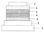
- FIG. 1 is a schematic cross-sectional view showing a structural example of the organic EL element used in the present invention.
- the organic EL element of the present invention has one or more light emitting layers between the facing anode and the cathode, and at least one of the light emitting layers is the thermally activated delayed fluorescence represented by the above general formula (1).
- Contains materials referred to as TADF materials.
- This organic EL device has a plurality of layers between the opposite anode and the cathode, and at least one of the plurality of layers is a light emitting layer, and the light emitting layer can contain a host material if necessary. Further, it can contain a luminescent dopant other than the thermally activated delayed fluorescent material represented by the general formula (1).
- the above general formula (1) will be described below.
- X 1 represents O or S. It preferably represents S.
- D is independently a nitrogen-containing heterocycle represented by the above formula (1a), and the ring Y in the above formula (1a) is the above formula (1a-1), (1a-2), or (1a-). It is any of 3), preferably the formula (1a-2) or (1a-3), and more preferably the formula (1a-3).
- the ring Y is of the above formula (1a-1)
- the ring Y is condensed at either the d or e position.
- the ring Y is of the above formula (1a-2
- the ring Y is condensed at the position of g.
- X 2 represents O, S, or N-Ar 2 , preferably N-Ar 2 .
- the ring Y is condensed at any position of i, j, or k, preferably at the position of i.
- a and b represent the number of permutations and represent an integer of 0 or 1, but a and b cannot be 0 at the same time.
- Ar 1 to Ar 3 are independently substituted or unsubstituted aromatic hydrocarbon groups having 6 to 18 carbon atoms, substituted or unsubstituted aromatic heterocyclic groups having 3 to 17 carbon atoms, or aromatic rings thereof.
- an unsubstituted aromatic hydrocarbon group having 6 to 15 carbon atoms, or an substituted or unsubstituted aromatic heterocyclic group having 3 to 15 carbon atoms, or 2 to 4 aromatic rings thereof are linked to each other.
- it is composed of an unsubstituted aromatic hydrocarbon group having 6 to 12 carbon atoms, an substituted or unsubstituted aromatic heterocyclic group having 3 to 12 carbon atoms, or a chain of 2 to 3 aromatic rings thereof. Represents a substituted or unsubstituted linked aromatic group to be substituted.
- unsubstituted Ar 1 to Ar 3 include benzene, naphthalene, acenaften, acenaphtylene, azulene, anthracene, chrysene, pyrene, phenanthrene, triphenylene, fluorene, benzo [a] anthracene, pyridine, pyrimidine, triazine, thiophene, Isothiazole, thiazole, pyridazine, pyrrol, pyrazole, imidazole, triazole, thiazylazole, pyrazine, furan, isoxazole, quinoline, isoquinoline, quinoxalin, quinazoline, thiazilazole, phthalazine, tetrazole, indol, benzofuran, benzothiophene, benzoxazole, benzothiazole, Indazole, benzimidazo
- a group produced by taking one hydrogen from the above can be mentioned.
- Each of these aromatic hydrocarbon groups, aromatic heterocyclic groups or linked aromatic groups may have a substituent.
- the substituents are a cyano group, an aliphatic hydrocarbon group having 1 to 10 carbon atoms, a diarylamino group having 12 to 44 carbon atoms, an alkoxy group having 1 to 10 carbon atoms, and 6 to 18 carbon atoms. It is an aryloxy group, an alkylthio group having 1 to 10 carbon atoms, and an arylthio group having 6 to 18 carbon atoms.
- the number of substituents is preferably 0 to 5, preferably 0 to 2.
- the carbon number calculation does not include the carbon number of the substituent. However, it is preferable that the total number of carbon atoms including the number of carbon atoms of the substituent satisfies the above range.
- substituents include cyano, methyl, ethyl, propyl, butyl, pentyl, hexyl, heptyl, octyl, nonyl, decyl, diphenylamino, naphthylphenylamino, dinaphthylamino, dianthranylamino and diphenan.
- substituents include cyano, methyl, ethyl, propyl, butyl, pentyl, hexyl, heptyl, octyl, nonyl, decyl, diphenylamino, naphthylphenylamino, dinaphthylamino, dianthranylamino and diphenan.
- examples thereof include threnylamino, dipyrenylamino, methoxy, ethoxy, phenol, diphenyloxy, methylthio, ethylthio, thi
- Preferred examples include cyano, methyl, ethyl, propyl, butyl, pentyl, hexyl, heptyl, octyl, diphenylamino, naphthylphenylamino, dinaphthylamino, phenol, or thiophenol.
- R 1 to R 4 are independently each of a heavy hydrogen, an aliphatic hydrocarbon group having 1 to 10 carbon atoms, an substituted or unsubstituted aromatic hydrocarbon group having 6 to 18 carbon atoms, or an aromatic hydrocarbon group having 3 to 17 carbon atoms. Represents an aromatic heterocyclic group.
- a heavy hydrogen, an aliphatic hydrocarbon group having 1 to 8 carbon atoms, a substituted or unsubstituted aromatic hydrocarbon group having 6 to 15 carbon atoms, or an aromatic heterocyclic group having 3 to 15 carbon atoms is preferable. show.
- c, f, h, and l represent integers from 0 to 4.
- R 1 to R 4 are aliphatic hydrocarbon groups having 1 to 10 carbon atoms
- R 1 to R 4 are aliphatic hydrocarbon groups having 1 to 10 carbon atoms
- Preferred examples include methyl, ethyl, propyl, butyl, pentyl, hexyl, heptyl and octyl.
- R 1 to R 4 are an substituted aromatic hydrocarbon group having 6 to 18 carbon atoms or an unsubstituted aromatic heterocyclic group having 3 to 17 carbon atoms include benzene, naphthalene, and acenaphene.
- Dibenzoselenovene a group produced by taking one hydrogen from carbazole. More preferably, benzene, naphthalene, azulene, pyridine, pyrimidine, triazine, thiophene, isothiazole, thiazole, pyridazine, pyrrole, pyrazole, imidazole, triazole, thiazylazole, pyrazine, furan, isoxazole, quinoline, isothiazole, quinoxalin, quinazoline, thiazylazole.
- Each of these aromatic hydrocarbon groups or aromatic heterocyclic groups may have a substituent.
- the substituent is a cyano group, an aliphatic hydrocarbon group having 1 to 10 carbon atoms, and a diarylamino group having 12 to 44 carbon atoms.
- the number of substituents is preferably 0 to 5, preferably 0 to 2.
- the carbon number calculation does not include the carbon number of the substituent. However, it is preferable that the total number of carbon atoms including the number of carbon atoms of the substituent satisfies the above range.
- substituents include cyano, methyl, ethyl, propyl, butyl, pentyl, hexyl, heptyl, octyl, nonyl, decyl, diphenylamino, naphthylphenylamino, dinaphthylamino, dianthranylamino and diphenan. Examples thereof include threnylamino and dipyrenylamino.
- Preferred examples include cyano, methyl, ethyl, propyl, butyl, pentyl, hexyl, heptyl, octyl, diphenylamino, naphthylphenylamino, or dinaphthylamino.
- thermally activated delayed fluorescent material represented by the general formula (1) Specific examples of the thermally activated delayed fluorescent material represented by the general formula (1) are shown below, but the present invention is not limited to these exemplified compounds.
- S1 and T1 are measured as follows.
- a sample compound thermalally activated delayed fluorescent material
- a quartz substrate by a vacuum vapor deposition method under the conditions of a vacuum degree of 10 -4 Pa or less to form a thin-film vapor deposition film with a thickness of 100 nm.
- S1 measures the emission spectrum of this vapor-deposited film, draws a tangent to the rising edge of the emission spectrum on the short wavelength side, and shows the wavelength value ⁇ edge [nm] at the intersection of the tangent and the horizontal axis in the following equation (i). Substitute in to calculate S1.
- S1 [eV] 1239.85 / ⁇ edge (i)
- T1 measures the phosphorescence spectrum of the vapor deposition film, draws a tangent to the rising edge of the phosphorescence spectrum on the short wavelength side, and formulates the wavelength value ⁇ edge [nm] at the intersection of the tangent and the horizontal axis (ii). Substitute in to calculate T1.
- T1 [eV] 1239.85 / ⁇ edge (ii)
- thermally activated delayed fluorescent material represented by the general formula (1) into the light emitting layer as a light emitting dopant or TADF material, an excellent delayed fluorescent organic EL element can be obtained.
- the light emitting layer can contain a host material together with the thermal activated delayed fluorescent material represented by the general formula (1). By containing the host material, it becomes an excellent organic EL element.
- the light emitting layer contains the thermally activated delayed fluorescent material represented by the general formula (1) and a fluorescent light emitting material other than the one represented by the general formula (1) as a light emitting dopant. Can be done. By containing a fluorescent light emitting material, it becomes an excellent organic EL element. In this case, the light emitting layer can further contain a host material.
- FIG. 1 is a cross-sectional view showing a structural example of a general organic EL device used in the present invention, in which 1 is a substrate, 2 is an anode, 3 is a hole injection layer, 4 is a hole transport layer, and 5 is a light emitting layer. , 6 represent an electron transport layer, and 7 represents a cathode.
- the organic EL device of the present invention may have an exciton blocking layer adjacent to the light emitting layer, or may have an electron blocking layer between the light emitting layer and the hole injection layer.
- the exciton blocking layer can be inserted into either the cathode side or the anode side of the light emitting layer, and both can be inserted at the same time.
- the organic EL device of the present invention has an anode, a light emitting layer, and a cathode as essential layers, but it is preferable to have a hole injection transport layer and an electron injection transport layer in addition to the essential layers, and further, a light emitting layer and an electron injection. It is preferable to have a hole blocking layer between the transport layers.
- the hole injection transport layer means either or both of the hole injection layer and the hole transport layer
- the electron injection transport layer means either or both of the electron injection layer and the electron transport layer.
- the structure opposite to that of FIG. 1, that is, the cathode 7, the electron transport layer 6, the light emitting layer 5, the hole transport layer 4, the hole injection layer 3, and the anode 2 can be laminated in this order on the substrate 1. In some cases, layers can be added or omitted as needed.
- the organic EL element as described above in addition to the electrodes such as the anode and the cathode, the layers constituting the laminated structure on the substrate may be collectively referred to as an organic layer.
- the organic EL element of the present invention is preferably supported by a substrate.
- the substrate is not particularly limited as long as it is conventionally used for an organic EL element, and for example, a substrate made of glass, transparent plastic, quartz or the like can be used.
- anode material in the organic EL element a material having a large work function (4 eV or more), an alloy, an electrically conductive compound, or a mixture thereof is preferably used.
- electrode materials include metals such as Au, and conductive transparent materials such as CuI, indium tin oxide (ITO), SnO 2, and ZnO.
- conductive transparent materials such as CuI, indium tin oxide (ITO), SnO 2, and ZnO.
- an amorphous material such as IDIXO (In 2 O 3- ZnO) capable of producing a transparent conductive film may be used.
- a thin film may be formed by forming a thin film of these electrode materials by a method such as thin film deposition or sputtering, and a pattern of a desired shape may be formed by a photolithography method, or when pattern accuracy is not required so much (about 100 ⁇ m or more).
- the pattern may be formed through a mask having a desired shape during vapor deposition or sputtering of the electrode material.
- a coatable substance such as an organic conductive compound
- a wet film forming method such as a printing method or a coating method can also be used.
- the sheet resistance as the anode is preferably several hundred ⁇ / ⁇ or less.
- the film thickness depends on the material, but is usually selected in the range of 10 to 1000 nm, preferably 10 to 200 nm.
- the cathode material a material consisting of a metal having a small work function (4 eV or less) (referred to as an electron-injectable metal), an alloy, an electrically conductive compound, or a mixture thereof is used.
- electrode materials include sodium, sodium-potassium alloy, magnesium, lithium, magnesium / copper mixture, magnesium / silver mixture, magnesium / aluminum mixture, magnesium / indium mixture, aluminum / aluminum oxide (Al 2 O). 3 ) Examples include mixtures, indium, lithium / aluminum mixtures, rare earth metals and the like.
- a mixture of an electron injectable metal and a second metal which is a stable metal having a larger work function value than this, for example, a magnesium / silver mixture, magnesium.
- a magnesium / silver mixture for example, magnesium.
- Aluminum mixture, magnesium / indium mixture, aluminum / aluminum oxide (Al 2 O 3 ) mixture, lithium / aluminum mixture, aluminum and the like are suitable.
- the cathode can be produced by forming a thin film of these cathode materials by a method such as vapor deposition or sputtering.
- the sheet resistance of the cathode is preferably several hundred ⁇ / ⁇ or less, and the film thickness is usually selected in the range of 10 nm to 5 ⁇ m, preferably 50 to 200 nm.
- the emission brightness is improved, which is convenient.
- a transparent or translucent cathode can be produced. By applying this, it is possible to manufacture an element in which both the anode and the cathode have transparency.
- the light emitting layer is a layer that emits light after excitons are generated by recombination of holes and electrons injected from the anode and the cathode, respectively.
- the TADF material represented by the general formula (1) may be used alone, or this TADF material may be used together with the host material. When a TADF material is used with a host material, the TADF material becomes a luminescent dopant. Further, the TADF material represented by the general formula (1) may be used together with a fluorescent light emitting material other than the material represented by the general formula (1). When used with a fluorescent material, it may be further used with a host material. When the TADF material represented by the general formula (1) is used together with the fluorescent light emitting material, the fluorescent light emitting material becomes a light emitting dopant.
- the content of the luminescent dopant is preferably 0.1 to 50 wt%, more preferably 0.1 to 40 wt% with respect to the host material.
- a known host material used in a phosphorescent light emitting element or a fluorescent light emitting element can be used.
- Known host materials that can be used are compounds having hole transporting ability and electron transporting ability and having a high glass transition temperature, and T1 is larger than T1 of the TADF material represented by the general formula (1). It is preferable to have.
- a TADF active compound may be used as the host material, in which case a compound having ⁇ EST of 0.20 eV or less is preferable.
- Anthracene derivatives fluorenone derivatives, stylben derivatives, triphenylene derivatives, carborane derivatives, porphyrin derivatives, phthalocyanine derivatives, metal complexes of 8-quinolinol derivatives and metal phthalocyanine, various metal complexes represented by metal complexes of benzoxazole and benzothiazole derivatives, poly Examples thereof include polymer compounds such as (N-vinylcarbazole) derivatives, aniline-based copolymers, thiophene oligomers, polythiophene derivatives, polyphenylene derivatives, polyphenylene vinylene derivatives, and polyfluorene derivatives.
- polymer compounds such as (N-vinylcarbazole) derivatives, aniline-based copolymers, thiophene oligomers, polythiophene derivatives, polyphenylene derivatives, polyphenylene vinylene derivatives, and polyfluorene derivatives.
- each host can be vapor-deposited from different vapor deposition sources, or multiple types of hosts can be simultaneously vapor-deposited from one vapor deposition source by premixing them before vapor deposition to form a premixture. ..
- a method capable of mixing as uniformly as possible is desirable, and examples thereof include pulverizing and mixing, heating and melting under reduced pressure or in an atmosphere of an inert gas such as nitrogen, sublimation, and the like. It is not limited to the method.
- the form of the host and its premixture may be powder, stick or granular.
- the preferred host is not particularly limited, but specific examples include the following.
- examples of the fluorescent light emitting material include a fused polycyclic aromatic derivative, a styrylamine derivative, a condensed ring amine derivative, and boron.
- examples thereof include compounds, pyrrole derivatives, indole derivatives, carbazole derivatives, indolecarbazole derivatives and the like.
- a fused ring amine derivative, a boron-containing compound, a carbazole derivative, and an indolocarbazole derivative are preferable.
- fused ring amine derivative examples include a diaminepyrene derivative, a diaminochrysene derivative, a diaminoanthracene derivative, a diaminofluorenone derivative, and a diaminofluorene derivative in which one or more benzoflo skeletons are fused.
- boron-containing compound examples include a pyrromethene derivative and a triphenylborane derivative.
- the preferable fluorescent light emitting material other than the one represented by the general formula (1) is not particularly limited, but specific examples thereof include the following.
- the injection layer is a layer provided between the electrode and the organic layer in order to reduce the driving voltage and improve the emission brightness.
- the injection layer includes a hole injection layer and an electron injection layer, and is located between the anode and the light emitting layer or the hole transport layer. And may be present between the cathode and the light emitting layer or the electron transporting layer.
- the injection layer can be provided as needed.
- the hole blocking layer has the function of an electron transporting layer in a broad sense, and is made of a hole blocking material having a function of transporting electrons and a significantly small ability to transport holes, and is composed of a hole blocking material while transporting electrons. It is possible to improve the recombination probability of electrons and holes in the light emitting layer by blocking the above.
- a known hole blocking material can be used for the hole blocking layer. Further, a plurality of types of hole blocking materials may be used in combination.
- the electron blocking layer has a function of a hole transporting layer in a broad sense, and by blocking electrons while transporting holes, the probability of recombination of electrons and holes in the light emitting layer can be improved. ..
- As the material of the electron blocking layer a known electron blocking layer material can be used.
- the exciton blocking layer is a layer for blocking excitons generated by recombination of holes and electrons in the light emitting layer from diffusing into the charge transport layer, and excitons are inserted by inserting this layer. It is possible to efficiently confine it in the light emitting layer, and it is possible to improve the light emitting efficiency of the element.
- the exciton blocking layer can be inserted between two adjacent light emitting layers in an element in which two or more light emitting layers are adjacent to each other. As the material of such an exciton blocking layer, a known exciton blocking layer material can be used.
- the layers adjacent to the light emitting layer include a hole blocking layer, an electron blocking layer, an exciton blocking layer, and the like, but if these layers are not provided, the hole transport layer, the electron transport layer, and the like are adjacent layers. Become.
- the hole transport layer is made of a hole transport material having a function of transporting holes, and the hole transport layer may be provided with a single layer or a plurality of layers.
- the hole transport material has any of hole injection, transport, and electron barrier properties, and may be either an organic substance or an inorganic substance. Any compound can be selected and used for the hole transport layer from conventionally known compounds. Examples of such hole transport materials include porphyrin derivatives, arylamine derivatives, triazole derivatives, oxadiazole derivatives, imidazole derivatives, polyarylalkane derivatives, phenylenediamine derivatives, arylamine derivatives, amino-substituted chalcone derivatives, oxazole derivatives, and styrylanthracene.
- Examples thereof include derivatives, fluorenone derivatives, hydrazone derivatives, stylben derivatives, silazane derivatives, aniline-based copolymers, and conductive polymer oligomers, especially thiophene oligomers, but porphyrin derivatives, arylamine derivatives and styrylamine derivatives may be used. It is preferable to use an arylamine compound, and it is more preferable to use an arylamine compound.
- the electron transport layer is made of a material having a function of transporting electrons, and the electron transport layer may be provided with a single layer or a plurality of layers.
- the electron transport material (which may also serve as a hole blocking material) may have a function of transmitting electrons injected from the cathode to the light emitting layer.
- any conventionally known compound can be selected and used, for example, a polycyclic aromatic derivative such as naphthalene, anthracene, phenanthroline, tris (8-quinolinolate) aluminum (III).
- Derivatives phosphine oxide derivatives, nitro-substituted fluorene derivatives, diphenylquinone derivatives, thiopyrandioxide derivatives, carbodiimide, fleolenilidene methane derivatives, anthracinodimethane and antron derivatives, bipyridine derivatives, quinoline derivatives, oxadiazole derivatives, benzoimidazole Derivatives, benzothiazole derivatives, indrocarbazole derivatives and the like can be mentioned. Further, a polymer material in which these materials are introduced into a polymer chain or these materials are used as a polymer main chain can also be used.
- the film forming method for each layer is not particularly limited, and it may be manufactured by either a dry process or a wet process.
- P (t-Bu) 3 / HBF 4 tri-tert-butylphosphonium tetrafluoroborate
- tert-BuONa sodium tert-butoxide
- toluene 42 ml in a three-necked flask, stir at 80 ° C for 15 minutes, and then bis (dibenzylideneacetone) palladium (0) [Pd (dba) 2 ] 0.12 g. was added, and the mixture was stirred at 110 ° C. for 30 minutes.
- Example 1 Each of the thin films shown below was laminated with a vacuum degree of 4.0 ⁇ 10 -5 Pa on a glass substrate having an anode made of ITO with a film thickness of 70 nm formed by a vacuum vapor deposition method.
- HAT-CN shown above as a hole injection layer was formed on ITO to a thickness of 10 nm, and then HT-1 was formed to a thickness of 25 nm as a hole transport layer.
- BH-1 was formed to a thickness of 5 nm as an electron blocking layer.
- BH-1 as a host and compound (1-15) as a dopant were co-deposited from different vapor deposition sources to form a light emitting layer having a thickness of 30 nm.
- HBL-1 was formed to a thickness of 5 nm as a hole blocking layer.
- ET-1 was formed to a thickness of 40 nm as an electron transport layer.
- lithium fluoride (LiF) was formed on the electron transport layer as an electron injection layer to a thickness of 1 nm.
- Al aluminum
- Example 2 An organic EL device was produced in the same manner as in Example 1 except that the dopant was compound (1-11).
- Example 3 An organic EL device was produced in the same manner as in Example 1 except that the dopant was compound (1-81).
- Example 4 Each of the thin films shown below was laminated with a vacuum degree of 4.0 ⁇ 10 -5 Pa on a glass substrate on which an anode made of ITO with a film thickness of 70 nm was formed by a vacuum vapor deposition method.
- HAT-CN shown above as a hole injection layer was formed on ITO to a thickness of 10 nm, and then HT-1 was formed to a thickness of 25 nm as a hole transport layer.
- BH-1 was formed to a thickness of 5 nm as an electron blocking layer.
- BH-1 as a host, compound (1-11) as a TADF material, and BD-1 as a dopant were co-deposited from different vapor deposition sources to form a light emitting layer having a thickness of 30 nm.
- co-deposited under the vapor deposition conditions where the concentration of BH-1 was 69% by mass, the concentration of compound (1-11) was 29%, and the concentration of BD-1 was 2% by mass.
- HBL-1 was formed to a thickness of 5 nm as a hole blocking layer.
- ET-1 was formed to a thickness of 40 nm as an electron transport layer.
- lithium fluoride (LiF) was formed on the electron transport layer as an electron injection layer to a thickness of 1 nm.
- aluminum (Al) was formed on the electron injection layer as a cathode to a thickness of 70 nm to produce an organic EL device according to Example 4.
- Comparative Example 1 An organic EL device was produced in the same manner as in Example 1 except that the dopant was TD-1.
- Table 2 shows the maximum emission wavelength, external quantum efficiency, and lifetime of the emission spectrum of the manufactured organic EL device.
- the maximum emission wavelength and external quantum efficiency are the values when the drive current density is 2.5 mA / cm 2, which are the initial characteristics.
- the life was measured by measuring the time until the brightness attenuated to 50% of the initial brightness when the initial brightness was 500 cd / m 2.
Abstract
Provided is a heat-activated delayed fluorescence-type organic EL element that is long lasting and that has high light emission efficiency. An organic EL element comprising a luminous layer between a positive electrode and a negative electrode facing each other, wherein a compound, in which a boron-containing electron acceptor backbone is linked with an electron donor backbone having a specific fused ring structure, is contained as a heat-activated delayed fluorescence material in at least one of the luminous layers, said compound is represented by general formula (1), and X1 in formula (1) represents O or S.
Description
本発明は、熱活性化遅延蛍光材料と、それを発光層に用いた有機電界発光素子(有機EL素子という)に関するものである。
The present invention relates to a thermally activated delayed fluorescent material and an organic electroluminescent device (referred to as an organic EL device) using the material as a light emitting layer.
有機EL素子に電圧を印加することで、陽極から正孔が、陰極からは電子がそれぞれ発光層に注入される。そして発光層において、注入された正孔と電子が再結合し、励起子が生成される。この際、電子スピンの統計則により、一重項励起子及び三重項励起子が1:3の割合で生成する。一重項励起子による発光を用いる蛍光発光型の有機EL素子は、内部量子効率は25%が限界であるといわれている。一方で三重項励起子による発光を用いる燐光発光型の有機EL素子は、一重項励起子から項間交差が効率的に行われた場合には、内部量子効率が100%まで高められることが知られている。
By applying a voltage to the organic EL element, holes are injected into the light emitting layer from the anode and electrons are injected from the cathode into the light emitting layer. Then, in the light emitting layer, the injected holes and electrons are recombined to generate excitons. At this time, singlet excitons and triplet excitons are generated at a ratio of 1: 3 according to the statistical law of electron spin. It is said that the internal quantum efficiency of a fluorescent light emitting type organic EL element using light emission by a singlet exciton is limited to 25%. On the other hand, it is known that the phosphorescent organic EL element that uses light emission by triplet excitons can increase the internal quantum efficiency to 100% when intersystem crossing is efficiently performed from the singlet excitons. Has been done.
近年では、燐光型有機EL素子の長寿命化技術が進展し、携帯電話等のディスプレイへ応用されつつある。しかしながら青色の有機EL素子に関しては、実用的な燐光発光型の有機EL素子は開発されておらず、高効率であり、且つ長寿命な青色有機EL素子の開発が求められている。
In recent years, technology for extending the life of phosphorescent organic EL devices has progressed and is being applied to displays such as mobile phones. However, as for the blue organic EL element, a practical phosphorescent type organic EL element has not been developed, and there is a demand for the development of a blue organic EL element having high efficiency and long life.
さらに最近では、遅延蛍光を利用した高効率の遅延蛍光型の有機EL素子の開発がなされている。例えば特許文献1には、遅延蛍光のメカニズムの1つであるTTF(Triplet-Triplet Fusion)機構を利用した有機EL素子が開示されている。TTF機構は2つの三重項励起子の衝突によって一重項励起子が生成する現象を利用するものであり、理論上内部量子効率を40%まで高められると考えられている。しかしながら、燐光発光型の有機EL素子と比較すると効率が低いため、更なる効率の改良が求められている。
More recently, a highly efficient delayed fluorescent organic EL device using delayed fluorescence has been developed. For example, Patent Document 1 discloses an organic EL device using a TTF (Triplet-Triplet Fusion) mechanism, which is one of the mechanisms of delayed fluorescence. The TTF mechanism utilizes the phenomenon that singlet excitons are generated by the collision of two triplet excitons, and it is theoretically thought that the internal quantum efficiency can be increased to 40%. However, since the efficiency is lower than that of the phosphorescent light emitting type organic EL element, further improvement in efficiency is required.
一方で特許文献2では、熱活性化遅延蛍光(TADF;Thermally Activated Delayed Fluorescence)機構を利用した有機EL素子が開示されている。TADF機構は一重項準位と三重項準位のエネルギー差が小さい材料において三重項励起子から一重項励起子への逆項間交差が生じる現象を利用するものであり、理論上内部量子効率を100%まで高められると考えられている。具体的に、特許文献2では、下記に示すようなインドロカルバゾール化合物からなる熱活性化遅延蛍光材料を開示している。

On the other hand, Patent Document 2 discloses an organic EL device using a Thermally Activated Delayed Fluorescence (TADF) mechanism. The TADF mechanism utilizes the phenomenon that reverse intersystem crossing from a triplet exciter to a singlet exciter occurs in a material with a small energy difference between the singlet level and the triplet level, and theoretically determines the internal quantum efficiency. It is believed that it can be increased to 100%. Specifically, Patent Document 2 discloses a thermally activated delayed fluorescent material composed of an indolocarbazole compound as shown below.
また、特許文献3では、下記に示すようなインドロカルバゾール化合物を遅延蛍光発光層に用いた有機電界発光素子を開示している。

Further, Patent Document 3 discloses an organic electroluminescent device using an indrocarbazole compound as shown below for a delayed fluorescent light emitting layer.
また、特許文献4では、下記に示すような熱活性化遅延蛍光材料を開示している。

Further, Patent Document 4 discloses a thermally activated delayed fluorescent material as shown below.
しかしながら、熱活性化遅延蛍光の有機EL素子についても燐光発光型の素子の場合と同様に寿命特性の更なる改善が求められている。つまり、このような熱活性化遅延蛍光発光材料を利用した遅延蛍光型の有機EL素子は、発光効率が高いという特徴があるが、更なる改良が求められている。
However, the organic EL element with thermal activated delayed fluorescence is also required to have further improved life characteristics as in the case of the phosphorescent light emitting type element. That is, a delayed fluorescent organic EL device using such a thermally activated delayed fluorescent light emitting material is characterized by high luminous efficiency, but further improvement is required.
有機EL素子をフラットパネルディスプレイ等の表示素子や光源として応用するためには、素子の発光効率を改善すると同時に駆動時の安定性を十分に確保する必要がある。本発明は、このような現状を鑑みてなされたものであり、高効率で発光し、且つ高い駆動安定性を有して実用上有用な有機EL素子を得ることができる熱活性化遅延蛍光材料、及びこれを用いた有機EL素子を提供することを目的とする。
In order to apply an organic EL element as a display element such as a flat panel display or a light source, it is necessary to improve the luminous efficiency of the element and at the same time ensure sufficient stability during driving. The present invention has been made in view of such a situation, and is a thermally activated delayed fluorescent material capable of obtaining a practically useful organic EL device having high efficiency of light emission and high drive stability. , And an organic EL device using the same.
すなわち、本発明は、下記一般式(1)で表される熱活性化遅延材料であり、また、本発明は、対向する陽極と陰極の間に1つ以上の発光層を含む有機EL素子において、少なくとも1つの発光層が、前記の熱活性化遅延蛍光材料を含有することを特徴とする有機EL素子である。

That is, the present invention is a thermally activated delayed material represented by the following general formula (1), and the present invention is an organic EL element including one or more light emitting layers between the opposing anode and cathode. , The organic EL element, characterized in that at least one light emitting layer contains the thermal activated delayed fluorescent material.
ここで、X1はO又はSを表す。
Dは独立に、式(1a)で表される含窒素複素環であり、
式(1a)中の*は前記一般式(1)の環と結合する位置を表し、また、環Yは、前記式(1a-1)、(1a-2)、又は(1a-3)のいずれかである。 Here, X 1 represents O or S.
D is independently a nitrogen-containing heterocycle represented by Eq. (1a).
* In the formula (1a) represents a position to be bonded to the ring of the general formula (1), and the ring Y is the position of the formula (1a-1), (1a-2), or (1a-3). Either.
環Yが前記式(1a-1)である場合、環Yはd又はeのいずれかの位置で縮合する。環Yが前記式(1a-2)である場合、環Yはgの位置で縮合し、X2はO、S、又はN-Ar2を表す。環Yが前記式(1a-3)である場合、環Yはi、j、又はkのいずれかの位置で縮合する。Ar1~Ar3は、置換若しくは未置換の炭素数6~18の芳香族炭化水素基、又は置換若しくは未置換の炭素数3~17の芳香族複素環基、又はこれらの芳香環が2~5個連結して構成される置換若しくは未置換の連結芳香族基を表す。R1~R4は重水素、炭素数1~10の脂肪族炭化水素基、置換若しくは未置換の炭素数6~18の芳香族炭化水素基、又は置換若しくは未置換の炭素数3~17の芳香族複素環基を表す。a、及びbは置換数を表し、0又は1の整数を表すが、a及びbが同時に0であることは無い。c、f、h、及びlは置換数を表し、0~4の整数を表す。
When the ring Y is of the above formula (1a-1), the ring Y is condensed at either the position of d or e. When the ring Y is of the above formula (1a-2), the ring Y is condensed at the position of g, and X 2 represents O, S, or N-Ar 2 . When the ring Y is of the above formula (1a-3), the ring Y is condensed at any of the positions i, j, or k. Ar 1 to Ar 3 are substituted or unsubstituted aromatic hydrocarbon groups having 6 to 18 carbon atoms, substituted or unsubstituted aromatic heterocyclic groups having 3 to 17 carbon atoms, or 2 to 2 of these aromatic rings. Represents a substituted or unsubstituted linked aromatic group composed of five linked aromatic groups. R 1 to R 4 are heavy hydrogens, aliphatic hydrocarbon groups having 1 to 10 carbon atoms, aromatic hydrocarbon groups having 6 to 18 substituted or unsubstituted carbon atoms, or substituted or unsubstituted aromatic hydrocarbon groups having 3 to 17 carbon atoms. Represents an aromatic heterocyclic group. a and b represent the number of permutations and represent an integer of 0 or 1, but a and b cannot be 0 at the same time. c, f, h, and l represent the number of permutations and represent integers from 0 to 4.
前記式(1a)において、環Yが前記式(1a-2)、又は(1a-3)で表されることが好ましい。
In the formula (1a), it is preferable that the ring Y is represented by the formula (1a-2) or (1a-3).
前記一般式(1)中のX1がSであることが好ましい。
It is preferable that X 1 in the general formula (1) is S.
また、前記一般式(1)で表される熱活性化遅延蛍光発光材料の一重項励起エネルギー(S1)と三重項励起エネルギー(T1)との差が0.20eVよりも小さいことがよく、好ましくは0.10eVよりも小さいことがよい。
Further, the difference between the singlet excitation energy (S1) and the triplet excitation energy (T1) of the thermally activated delayed fluorescent material represented by the general formula (1) is preferably smaller than 0.20 eV, preferably. It should be less than 0.10 eV.
本発明の熱活性化遅延蛍光材料によれば、これを発光層に含有させることで、高発光効率、且つ長寿命な有機EL素子を提供することができるようになる。
According to the thermally activated delayed fluorescent material of the present invention, by incorporating this into the light emitting layer, it becomes possible to provide an organic EL device having high luminous efficiency and long life.
本発明の有機EL素子は、対向する陽極と陰極の間に、1つ以上の発光層を有し、発光層の少なくとも1層が、上記一般式(1)で表される熱活性化遅延蛍光材料(TADF材料という。)を含有する。この有機EL素子は、対向する陽極と陰極の間に複数の層を有するが、複数の層の少なくとも1層は発光層であり、発光層には必要によりホスト材料を含有することができる。
さらに、上記一般式(1)で表される熱活性化遅延蛍光材料以外の発光性ドーパントを含有することができる。
上記一般式(1)について、以下で説明する。 The organic EL element of the present invention has one or more light emitting layers between the facing anode and the cathode, and at least one of the light emitting layers is the thermally activated delayed fluorescence represented by the above general formula (1). Contains materials (referred to as TADF materials). This organic EL device has a plurality of layers between the opposite anode and the cathode, and at least one of the plurality of layers is a light emitting layer, and the light emitting layer can contain a host material if necessary.
Further, it can contain a luminescent dopant other than the thermally activated delayed fluorescent material represented by the general formula (1).
The above general formula (1) will be described below.
先ず、X1はO又はSを表す。好ましくはSを表す。
First, X 1 represents O or S. It preferably represents S.
Dは独立に、前記式(1a)で表される含窒素複素環であり、前記式(1a)中の環Yは、前記式(1a-1)、(1a-2)、又は(1a-3)のいずれかであり、好ましくは、式(1a-2)又は(1a-3)であり、より好ましくは式(1a-3)である。環Yが前記式(1a-1)である場合、環Yはd、又はeのいずれかの位置で縮合する。環Yが前記式(1a-2)である場合、環Yはgの位置で縮合する。X2はO、S、又はN-Ar2を表し、好ましくはN-Ar2を表す。環Yが前記式(1a-3)である場合、環Yはi、j、又はkのいずれかの位置で縮合し、好ましくはiの位置で縮合する。a、及びbは置換数を表し、0又は1の整数を表すが、a及びbが同時に0であることは無い。
D is independently a nitrogen-containing heterocycle represented by the above formula (1a), and the ring Y in the above formula (1a) is the above formula (1a-1), (1a-2), or (1a-). It is any of 3), preferably the formula (1a-2) or (1a-3), and more preferably the formula (1a-3). When the ring Y is of the above formula (1a-1), the ring Y is condensed at either the d or e position. When the ring Y is of the above formula (1a-2), the ring Y is condensed at the position of g. X 2 represents O, S, or N-Ar 2 , preferably N-Ar 2 . When the ring Y is of the above formula (1a-3), the ring Y is condensed at any position of i, j, or k, preferably at the position of i. a and b represent the number of permutations and represent an integer of 0 or 1, but a and b cannot be 0 at the same time.
Ar1~Ar3は、それぞれ独立に置換若しくは未置換の炭素数6~18の芳香族炭化水素基、又は置換若しくは未置換の炭素数3~17の芳香族複素環基、又はこれらの芳香環が2~5個連結して構成される置換若しくは未置換の連結芳香族基を表す。好ましくは未置換の炭素数6~15の芳香族炭化水素基、又は置換若しくは未置換の炭素数3~15の芳香族複素環基、又はこれらの芳香環が2~4個連結して構成される置換若しくは未置換の連結芳香族基を表す。より好ましくは未置換の炭素数6~12の芳香族炭化水素基、又は置換若しくは未置換の炭素数3~12の芳香族複素環基、又はこれらの芳香環が2~3個連結して構成される置換若しくは未置換の連結芳香族基を表す。
Ar 1 to Ar 3 are independently substituted or unsubstituted aromatic hydrocarbon groups having 6 to 18 carbon atoms, substituted or unsubstituted aromatic heterocyclic groups having 3 to 17 carbon atoms, or aromatic rings thereof. Represents a substituted or unsubstituted linked aromatic group composed of 2 to 5 linked aromatic groups. Preferably, an unsubstituted aromatic hydrocarbon group having 6 to 15 carbon atoms, or an substituted or unsubstituted aromatic heterocyclic group having 3 to 15 carbon atoms, or 2 to 4 aromatic rings thereof are linked to each other. Represents a substituted or unsubstituted linked aromatic group. More preferably, it is composed of an unsubstituted aromatic hydrocarbon group having 6 to 12 carbon atoms, an substituted or unsubstituted aromatic heterocyclic group having 3 to 12 carbon atoms, or a chain of 2 to 3 aromatic rings thereof. Represents a substituted or unsubstituted linked aromatic group to be substituted.
未置換のAr1~Ar3の具体例としては、ベンゼン、ナフタレン、アセナフテン、アセナフチレン、アズレン、アントラセン、クリセン、ピレン、フェナントレン、トリフェニレン、フルオレン、ベンゾ[a]アントラセン、ピリジン、ピリミジン、トリアジン、チオフェン、イソチアゾール、チアゾール、ピリダジン、ピロール、ピラゾール、イミダゾール、トリアゾール、チアジアゾール、ピラジン、フラン、イソキサゾール、キノリン、イソキノリン、キノキサリン、キナゾリン、チアジアゾール、フタラジン、テトラゾール、インドール、ベンゾフラン、ベンゾチオフェン、ベンゾオキサゾール、ベンゾチアゾール、インダゾール、ベンズイミダゾール、ベンゾトリアゾール、ベンゾイソチアゾール、ベンゾチアジアゾール、プリン、ピラノン、クマリン、イソクマリン、クロモン、ジベンゾフラン、ジベンゾチオフェン、ジベンゾセレノフェン、カルバゾール、又はこれらが2~5個連結して構成される化合物から1個の水素を取って生じる基が挙げられる。好ましくは、ベンゼン、ナフタレン、アセナフテン、アセナフチレン、アズレン、アントラセン、フェナントレン、フルオレン、ピリジン、ピリミジン、トリアジン、チオフェン、イソチアゾール、チアゾール、ピリダジン、ピロール、ピラゾール、イミダゾール、トリアゾール、チアジアゾール、ピラジン、フラン、イソキサゾール、キノリン、イソキノリン、キノキサリン、キナゾリン、チアジアゾール、フタラジン、テトラゾール、インドール、ベンゾフラン、ベンゾチオフェン、ベンゾオキサゾール、ベンゾチアゾール、インダゾール、ベンズイミダゾール、ベンゾトリアゾール、ベンゾイソチアゾール、ベンゾチアジアゾール、プリン、ピラノン、クマリン、イソクマリン、クロモン、ジベンゾフラン、ジベンゾチオフェン、ジベンゾセレノフェン、カルバゾール、又はこれらが2~4個連結して構成される化合物から1個の水素を取って生じる基が挙げられる。より好ましくは、ベンゼン、ナフタレン、アセナフテン、アセナフチレン、アズレン、ピリジン、ピリミジン、トリアジン、チオフェン、イソチアゾール、チアゾール、ピリダジン、ピロール、ピラゾール、イミダゾール、トリアゾール、チアジアゾール、ピラジン、フラン、イソキサゾール、キノリン、イソキノリン、キノキサリン、キナゾリン、チアジアゾール、フタラジン、テトラゾール、インドール、ベンゾフラン、ベンゾチオフェン、ベンゾオキサゾール、ベンゾチアゾール、インダゾール、ベンズイミダゾール、ベンゾトリアゾール、ベンゾイソチアゾール、ベンゾチアジアゾール、プリン、ピラノン、クマリン、イソクマリン、クロモン、ジベンゾフラン、ジベンゾチオフェン、ジベンゾセレノフェン、カルバゾール、又はこれらが2~3連結して構成される化合物から1個の水素を取って生じる基が挙げられる。
Specific examples of the unsubstituted Ar 1 to Ar 3 include benzene, naphthalene, acenaften, acenaphtylene, azulene, anthracene, chrysene, pyrene, phenanthrene, triphenylene, fluorene, benzo [a] anthracene, pyridine, pyrimidine, triazine, thiophene, Isothiazole, thiazole, pyridazine, pyrrol, pyrazole, imidazole, triazole, thiazylazole, pyrazine, furan, isoxazole, quinoline, isoquinoline, quinoxalin, quinazoline, thiazilazole, phthalazine, tetrazole, indol, benzofuran, benzothiophene, benzoxazole, benzothiazole, Indazole, benzimidazole, benzotriazole, benzoisothiazole, benzothiazole, purine, pyranone, coumarin, isothiazole, chromon, dibenzofuran, dibenzothiophene, dibenzoselenovene, carbazole, or a compound composed of 2 to 5 of these linked together. A group produced by taking one hydrogen from the above can be mentioned. Preferably, benzene, naphthalene, acenaften, acenaphtylene, azulene, anthracene, phenanthrene, fluorene, pyridine, pyrimidine, triazine, thiophene, isothiazole, thiazole, pyridazine, pyrrole, pyrazole, imidazole, triazole, thiadiazol, pyrazine, furan, isoxazole, Kinolin, isoquinoline, quinoxalin, quinazoline, thiazylazole, phthalazine, tetrazole, indole, benzofuran, benzothiophene, benzoxazole, benzothiazole, indazole, benzimidazole, benzotriazole, benzoisothiazole, benzothiazole, purine, pyranone, coumarin, isocmarin, Examples thereof include chromone, dibenzofuran, dibenzothiophene, dibenzoselenophene, carbazole, or a group formed by taking one hydrogen from a compound composed of two to four linked compounds thereof. More preferably, benzene, naphthalene, acenaften, acenaphtylene, azulene, pyridine, pyrimidine, triazine, thiophene, isothiazole, thiazole, pyridazine, pyrrol, pyrazole, imidazole, triazole, thiaziazol, pyrazine, furan, isoxazole, quinoline, isoquinoline, quinoxalin. , Kinazoline, thiazylazole, phthalazine, tetrazole, indol, benzofuran, benzothiophene, benzoxazole, benzothiazole, indazole, benzimidazole, benzotriazole, benzoisothiazole, benzothiazole, purine, pyranone, coumarin, isocmarin, chromon, dibenzofuran, dibenzo Examples thereof include thiophene, dibenzoselenophene, carbazole, or a group formed by taking one hydrogen from a compound composed of two or three linkages thereof.
これら芳香族炭化水素基、芳香族複素環基又は連結芳香族基は、それぞれ置換基を有してもよい。置換基を有する場合の置換基は、シアノ基、炭素数1~10の脂肪族炭化水素基、炭素数12~44のジアリールアミノ基、炭素数1~10のアルコキシ基、炭素数6~18のアリールオキシ基、炭素数1~10のアルキルチオ基、炭素数6~18のアリールチオ基である。なお、置換基の数は0~5、好ましくは0~2がよい。芳香族炭化水素基及び芳香族複素環基が置換基を有する場合の炭素数の計算には、置換基の炭素数を含まない。しかし、置換基の炭素数を含んだ合計の炭素数が上記範囲を満足することが好ましい。
Each of these aromatic hydrocarbon groups, aromatic heterocyclic groups or linked aromatic groups may have a substituent. When having a substituent, the substituents are a cyano group, an aliphatic hydrocarbon group having 1 to 10 carbon atoms, a diarylamino group having 12 to 44 carbon atoms, an alkoxy group having 1 to 10 carbon atoms, and 6 to 18 carbon atoms. It is an aryloxy group, an alkylthio group having 1 to 10 carbon atoms, and an arylthio group having 6 to 18 carbon atoms. The number of substituents is preferably 0 to 5, preferably 0 to 2. When the aromatic hydrocarbon group and the aromatic heterocyclic group have a substituent, the carbon number calculation does not include the carbon number of the substituent. However, it is preferable that the total number of carbon atoms including the number of carbon atoms of the substituent satisfies the above range.
上記置換基の具体例としては、シアノ、メチル、エチル、プロピル、ブチル、ペンチル、へキシル、ヘプチル、オクチル、ノニル、デシル、ジフェニルアミノ、ナフチルフェニルアミノ、ジナフチルアミノ、ジアントラニルアミノ、ジフェナンスレニルアミノ、ジピレニルアミノ、メトキシ、エトキシ、フェノール、ジフェニルオキシ、メチルチオ、エチルチオ、チオフェノール、又はジフェニルチオが挙げられる。好ましくは、シアノ、メチル、エチル、プロピル、ブチル、ペンチル、へキシル、ヘプチル、オクチル、ジフェニルアミノ、ナフチルフェニルアミノ、ジナフチルアミノ、フェノール、又はチオフェノールが挙げられる。
Specific examples of the above substituents include cyano, methyl, ethyl, propyl, butyl, pentyl, hexyl, heptyl, octyl, nonyl, decyl, diphenylamino, naphthylphenylamino, dinaphthylamino, dianthranylamino and diphenan. Examples thereof include threnylamino, dipyrenylamino, methoxy, ethoxy, phenol, diphenyloxy, methylthio, ethylthio, thiophenol, or diphenylthio. Preferred examples include cyano, methyl, ethyl, propyl, butyl, pentyl, hexyl, heptyl, octyl, diphenylamino, naphthylphenylamino, dinaphthylamino, phenol, or thiophenol.
R1~R4は、それぞれ独立に、重水素、炭素数1~10の脂肪族炭化水素基、置換若しくは未置換の炭素数6~18の芳香族炭化水素基、又は炭素数3~17の芳香族複素環基を表す。このうち好ましくは、重水素、炭素数1~8の脂肪族炭化水素基、置換若しくは未置換の炭素数6~15の芳香族炭化水素基、又は炭素数3~15の芳香族複素環基を表す。より好ましくは、炭素数1~6の脂肪族炭化水素基、置換若しくは未置換の炭素数6~12の芳香族炭化水素基、又は炭素数3~12の芳香族複素環基を表す。c、f、h、及びlは0~4の整数を表す。
R 1 to R 4 are independently each of a heavy hydrogen, an aliphatic hydrocarbon group having 1 to 10 carbon atoms, an substituted or unsubstituted aromatic hydrocarbon group having 6 to 18 carbon atoms, or an aromatic hydrocarbon group having 3 to 17 carbon atoms. Represents an aromatic heterocyclic group. Of these, a heavy hydrogen, an aliphatic hydrocarbon group having 1 to 8 carbon atoms, a substituted or unsubstituted aromatic hydrocarbon group having 6 to 15 carbon atoms, or an aromatic heterocyclic group having 3 to 15 carbon atoms is preferable. show. More preferably, it represents an aliphatic hydrocarbon group having 1 to 6 carbon atoms, an substituted or unsubstituted aromatic hydrocarbon group having 6 to 12 carbon atoms, or an aromatic heterocyclic group having 3 to 12 carbon atoms. c, f, h, and l represent integers from 0 to 4.
R1~R4が炭素数1~10の脂肪族炭化水素基である場合の具体例としては、メチル、エチル、プロピル、ブチル、ペンチル、へキシル、ヘプチル、オクチル、ノニルが挙げられる。好ましくは、メチル、エチル、プロピル、ブチル、ペンチル、へキシル、ヘプチル、オクチルが挙げられる。
Specific examples of cases where R 1 to R 4 are aliphatic hydrocarbon groups having 1 to 10 carbon atoms include methyl, ethyl, propyl, butyl, pentyl, hexyl, heptyl, octyl, and nonyl. Preferred examples include methyl, ethyl, propyl, butyl, pentyl, hexyl, heptyl and octyl.
R1~R4が未置換の炭素数6~18の芳香族炭化水素基、又は未置換の炭素数3~17の芳香族複素環基である場合の具体例としては、ベンゼン、ナフタレン、アセナフテン、アセナフチレン、アズレン、アントラセン、クリセン、ピレン、フェナントレン、トリフェニレン、フルオレン、ベンゾ[a]アントラセン、ピリジン、ピリミジン、トリアジン、チオフェン、イソチアゾール、チアゾール、ピリダジン、ピロール、ピラゾール、イミダゾール、トリアゾール、チアジアゾール、ピラジン、フラン、イソキサゾール、キノリン、イソキノリン、キノキサリン、キナゾリン、チアジアゾール、フタラジン、テトラゾール、インドール、ベンゾフラン、ベンゾチオフェン、ベンゾオキサゾール、ベンゾチアゾール、インダゾール、ベンズイミダゾール、ベンゾトリアゾール、ベンゾイソチアゾール、ベンゾチアジアゾール、プリン、ピラノン、クマリン、イソクマリン、クロモン、ジベンゾフラン、ジベンゾチオフェン、ジベンゾセレノフェン、カルバゾールから1個の水素を取って生じる基が挙げられる。好ましくは、ベンゼン、ナフタレン、アセナフテン、アセナフチレン、アズレン、ピリジン、ピリミジン、トリアジン、チオフェン、イソチアゾール、チアゾール、ピリダジン、ピロール、ピラゾール、イミダゾール、トリアゾール、チアジアゾール、ピラジン、フラン、イソキサゾール、キノリン、イソキノリン、キノキサリン、キナゾリン、チアジアゾール、フタラジン、テトラゾール、インドール、ベンゾフラン、ベンゾチオフェン、ベンゾオキサゾール、ベンゾチアゾール、インダゾール、ベンズイミダゾール、ベンゾトリアゾール、ベンゾイソチアゾール、ベンゾチアジアゾール、プリン、ピラノン、クマリン、イソクマリン、クロモン、ジベンゾフラン、ジベンゾチオフェン、ジベンゾセレノフェン、カルバゾールから1個の水素を取って生じる基が挙げられる。より好ましくは、ベンゼン、ナフタレン、アズレン、ピリジン、ピリミジン、トリアジン、チオフェン、イソチアゾール、チアゾール、ピリダジン、ピロール、ピラゾール、イミダゾール、トリアゾール、チアジアゾール、ピラジン、フラン、イソキサゾール、キノリン、イソキノリン、キノキサリン、キナゾリン、チアジアゾール、フタラジン、テトラゾール、インドール、ベンゾフラン、ベンゾチオフェン、ベンゾオキサゾール、ベンゾチアゾール、インダゾール、ベンズイミダゾール、ベンゾトリアゾール、ベンゾイソチアゾール、ベンゾチアジアゾール、プリン、ピラノン、クマリン、イソクマリン、クロモン、ジベンゾフラン、ジベンゾチオフェン、ジベンゾセレノフェン、カルバゾールから1個の水素を取って生じる基が挙げられる。
Specific examples of cases where R 1 to R 4 are an substituted aromatic hydrocarbon group having 6 to 18 carbon atoms or an unsubstituted aromatic heterocyclic group having 3 to 17 carbon atoms include benzene, naphthalene, and acenaphene. , Asenaftylene, azulene, anthracene, chrysen, pyrene, phenanthrene, triphenylene, fluorene, benzo [a] anthracene, pyridine, pyrimidine, triazine, thiophene, isothiazole, thiazole, pyridazine, pyrrol, pyrazole, imidazole, triazole, thiadiazole, pyrazine, Fran, isoxazole, quinoline, isoquinoline, quinoxalin, quinazoline, thiadiazole, phthalazine, tetrazole, indole, benzofuran, benzothiophene, benzoxazole, benzothiazole, indazole, benzimidazole, benzotriazole, benzoisothiazole, benzothiazol, purine, pyranone, Examples thereof include groups formed by taking one hydrogen from coumarin, isocoumarin, chromon, dibenzofuran, dibenzothiophene, dibenzoselenophen, and carbazole. Preferably, benzene, naphthalene, acenaften, acenaphtylene, azulene, pyridine, pyrimidine, triazine, thiophene, isothiazole, thiazole, pyridazine, pyrrole, pyrazole, imidazole, triazole, thiaziazole, pyrazine, furan, isoxazole, quinoline, isoquinoline, quinoxalin, Kinazoline, thiazylazole, phthalazine, tetrazole, indol, benzofuran, benzothiophene, benzoxazole, benzothiazole, indazole, benzimidazole, benzotriazole, benzoisothiazole, benzothiazole, purine, pyranone, coumarin, isothiazole, chromon, dibenzofuran, dibenzothiophene. , Dibenzoselenovene, a group produced by taking one hydrogen from carbazole. More preferably, benzene, naphthalene, azulene, pyridine, pyrimidine, triazine, thiophene, isothiazole, thiazole, pyridazine, pyrrole, pyrazole, imidazole, triazole, thiazylazole, pyrazine, furan, isoxazole, quinoline, isothiazole, quinoxalin, quinazoline, thiazylazole. , Phthalazine, tetrazole, indole, benzofuran, benzothiophene, benzoxazole, benzothiazole, indazole, benzimidazole, benzotriazole, benzoisothiazole, benzothiazol, purine, pyranone, coumarin, isocmarin, chromon, dibenzofuran, dibenzothiophene, dibenzoseleno Examples thereof include a group formed by taking one hydrogen from fen and carbazole.
これら芳香族炭化水素基又は芳香族複素環基は、それぞれ置換基を有してもよい。置換基を有する場合の置換基は、シアノ基、炭素数1~10の脂肪族炭化水素基、炭素数12~44のジアリールアミノ基である。なお、置換基の数は0~5、好ましくは0~2がよい。芳香族炭化水素基及び芳香族複素環基が置換基を有する場合の炭素数の計算には、置換基の炭素数を含まない。しかし、置換基の炭素数を含んだ合計の炭素数が上記範囲を満足することが好ましい。
Each of these aromatic hydrocarbon groups or aromatic heterocyclic groups may have a substituent. When having a substituent, the substituent is a cyano group, an aliphatic hydrocarbon group having 1 to 10 carbon atoms, and a diarylamino group having 12 to 44 carbon atoms. The number of substituents is preferably 0 to 5, preferably 0 to 2. When the aromatic hydrocarbon group and the aromatic heterocyclic group have a substituent, the carbon number calculation does not include the carbon number of the substituent. However, it is preferable that the total number of carbon atoms including the number of carbon atoms of the substituent satisfies the above range.
上記置換基の具体例としては、シアノ、メチル、エチル、プロピル、ブチル、ペンチル、へキシル、ヘプチル、オクチル、ノニル、デシル、ジフェニルアミノ、ナフチルフェニルアミノ、ジナフチルアミノ、ジアントラニルアミノ、ジフェナンスレニルアミノ、ジピレニルアミノが挙げられる。好ましくは、シアノ、メチル、エチル、プロピル、ブチル、ペンチル、へキシル、ヘプチル、オクチル、ジフェニルアミノ、ナフチルフェニルアミノ、又はジナフチルアミノが挙げられる。
Specific examples of the above substituents include cyano, methyl, ethyl, propyl, butyl, pentyl, hexyl, heptyl, octyl, nonyl, decyl, diphenylamino, naphthylphenylamino, dinaphthylamino, dianthranylamino and diphenan. Examples thereof include threnylamino and dipyrenylamino. Preferred examples include cyano, methyl, ethyl, propyl, butyl, pentyl, hexyl, heptyl, octyl, diphenylamino, naphthylphenylamino, or dinaphthylamino.
一般式(1)で表される熱活性化遅延蛍光材料の具体的な例を以下に示すが、これら例示化合物に限定されるものではない。
Specific examples of the thermally activated delayed fluorescent material represented by the general formula (1) are shown below, but the present invention is not limited to these exemplified compounds.


前記一般式(1)で表される熱活性化遅延蛍光材料は、一重項励起エネルギー(S1)と三重項励起エネルギー(T1)との差(ΔEST=S1-T1)が0.20eVよりも小さいものであることが好ましく、0.10eVよりも小さいものであることがより好ましい。
The thermally activated delayed fluorescent material represented by the general formula (1) has a difference (ΔEST = S1-T1) between the singlet excitation energy (S1) and the triplet excitation energy (T1) smaller than 0.20 eV. It is preferably less than 0.10 eV, and more preferably less than 0.10 eV.
ここで、S1、T1は次のようにして測定される。
石英基板上に真空蒸着法にて、真空度10-4Pa以下の条件にて試料化合物(熱活性化遅延蛍光材料)を蒸着し、蒸着膜を100nmの厚さで形成する。S1は、この蒸着膜の発光スペクトルを測定し、発光スペクトルの短波長側の立ち上がりに対して接線を引き、その接線と横軸の交点の波長値λedge[nm]を次に示す式(i)に代入してS1を算出する。
S1[eV] = 1239.85/λedge (i) Here, S1 and T1 are measured as follows.
A sample compound (thermally activated delayed fluorescent material) is deposited on a quartz substrate by a vacuum vapor deposition method under the conditions of a vacuum degree of 10 -4 Pa or less to form a thin-film vapor deposition film with a thickness of 100 nm. S1 measures the emission spectrum of this vapor-deposited film, draws a tangent to the rising edge of the emission spectrum on the short wavelength side, and shows the wavelength value λedge [nm] at the intersection of the tangent and the horizontal axis in the following equation (i). Substitute in to calculate S1.
S1 [eV] = 1239.85 / λedge (i)
一方のT1は、前記蒸着膜の燐光スペクトルを測定し、この燐光スペクトルの短波長側の立ち上がりに対して接線を引き、その接線と横軸の交点の波長値λedge[nm]を式(ii)に代入してT1を算出する。
T1[eV] = 1239.85/λedge (ii) On the other hand, T1 measures the phosphorescence spectrum of the vapor deposition film, draws a tangent to the rising edge of the phosphorescence spectrum on the short wavelength side, and formulates the wavelength value λedge [nm] at the intersection of the tangent and the horizontal axis (ii). Substitute in to calculate T1.
T1 [eV] = 1239.85 / λedge (ii)
前記一般式(1)で表される熱活性化遅延蛍光材料を発光性ドーパント、又はTADF材料として、発光層に含有させることで優れた遅延蛍光型の有機EL素子とすることができる。
By incorporating the thermally activated delayed fluorescent material represented by the general formula (1) into the light emitting layer as a light emitting dopant or TADF material, an excellent delayed fluorescent organic EL element can be obtained.
また、発光層には必要により、前記一般式(1)で表される熱活性化遅延蛍光材料と共にホスト材料を含有させることができる。ホスト材料を含有させることにより、優れた有機EL素子となる。
Further, if necessary, the light emitting layer can contain a host material together with the thermal activated delayed fluorescent material represented by the general formula (1). By containing the host material, it becomes an excellent organic EL element.
また、発光層には必要により、前記一般式(1)で表される熱活性化遅延蛍光材料と共に前記一般式(1)で表されるもの以外の蛍光発光材料を発光性ドーパントとして含有させることができる。蛍光発光材料を含有させることにより、優れた有機EL素子となる。この場合、発光層には更にホスト材料を含有させることができる。
Further, if necessary, the light emitting layer contains the thermally activated delayed fluorescent material represented by the general formula (1) and a fluorescent light emitting material other than the one represented by the general formula (1) as a light emitting dopant. Can be done. By containing a fluorescent light emitting material, it becomes an excellent organic EL element. In this case, the light emitting layer can further contain a host material.
次に、本発明の有機EL素子の構造について、図面を参照しながら説明するが、本発明の有機EL素子の構造はこれに限定されない。
Next, the structure of the organic EL element of the present invention will be described with reference to the drawings, but the structure of the organic EL element of the present invention is not limited to this.
図1は本発明に用いられる一般的な有機EL素子の構造例を示す断面図であり、1は基板、2は陽極、3は正孔注入層、4は正孔輸送層、5は発光層、6は電子輸送層、7は陰極を表す。本発明の有機EL素子は発光層と隣接して励起子阻止層を有してもよく、また発光層と正孔注入層との間に電子阻止層を有してもよい。励起子阻止層は発光層の陰極側、陽極側のいずれにも挿入することができ、両方同時に挿入することも可能である。本発明の有機EL素子では、陽極、発光層、そして陰極を必須の層として有するが、必須の層以外に正孔注入輸送層、電子注入輸送層を有することがよく、更に発光層と電子注入輸送層の間に正孔阻止層を有することがよい。なお、正孔注入輸送層は、正孔注入層と正孔輸送層のいずれか、または両者を意味し、電子注入輸送層は、電子注入層と電子輸送層のいずれかまたは両者を意味する。
FIG. 1 is a cross-sectional view showing a structural example of a general organic EL device used in the present invention, in which 1 is a substrate, 2 is an anode, 3 is a hole injection layer, 4 is a hole transport layer, and 5 is a light emitting layer. , 6 represent an electron transport layer, and 7 represents a cathode. The organic EL device of the present invention may have an exciton blocking layer adjacent to the light emitting layer, or may have an electron blocking layer between the light emitting layer and the hole injection layer. The exciton blocking layer can be inserted into either the cathode side or the anode side of the light emitting layer, and both can be inserted at the same time. The organic EL device of the present invention has an anode, a light emitting layer, and a cathode as essential layers, but it is preferable to have a hole injection transport layer and an electron injection transport layer in addition to the essential layers, and further, a light emitting layer and an electron injection. It is preferable to have a hole blocking layer between the transport layers. The hole injection transport layer means either or both of the hole injection layer and the hole transport layer, and the electron injection transport layer means either or both of the electron injection layer and the electron transport layer.
図1とは逆の構造、すなわち基板1上に陰極7、電子輸送層6、発光層5、正孔輸送層4、正孔注入層3、陽極2の順に積層することも可能であり、この場合も必要により層を追加、省略することが可能である。なお、上述したような有機EL素子において、陽極や陰極のような電極以外に基板上で積層構造を構成する層をまとめて有機層という場合がある。
The structure opposite to that of FIG. 1, that is, the cathode 7, the electron transport layer 6, the light emitting layer 5, the hole transport layer 4, the hole injection layer 3, and the anode 2 can be laminated in this order on the substrate 1. In some cases, layers can be added or omitted as needed. In the organic EL element as described above, in addition to the electrodes such as the anode and the cathode, the layers constituting the laminated structure on the substrate may be collectively referred to as an organic layer.
-基板-
本発明の有機EL素子は、基板に支持されていることが好ましい。この基板については特に制限はなく、従来から有機EL素子に用いられているものであればよく、例えばガラス、透明プラスチック、石英等からなるものを用いることができる。 -substrate-
The organic EL element of the present invention is preferably supported by a substrate. The substrate is not particularly limited as long as it is conventionally used for an organic EL element, and for example, a substrate made of glass, transparent plastic, quartz or the like can be used.
-陽極-
有機EL素子における陽極材料としては、仕事関数の大きい(4eV以上)金属、合金、電気伝導性化合物又はこれらの混合物からなる材料が好ましく用いられる。このような電極材料の具体例としてはAu等の金属、CuI、インジウムチンオキシド(ITO)、SnO2、ZnO等の導電性透明材料が挙げられる。また、IDIXO(In2O3-ZnO)等の非晶質で、透明導電膜を作製可能な材料を用いてもよい。陽極はこれらの電極材料を蒸着やスパッタリング等の方法により薄膜を形成させ、フォトリソグラフィー法で所望の形状のパターンを形成してもよく、あるいはパターン精度をあまり必要としない場合(100μm以上程度)は、上記電極材料の蒸着やスパッタリング時に所望の形状のマスクを介してパターンを形成してもよい。あるいは有機導電性化合物のような塗布可能な物質を用いる場合には印刷方式、コーティング方式等湿式成膜法を用いることもできる。この陽極より発光を取り出す場合には、透過率を10%より大きくすることが望ましく、また、陽極としてのシート抵抗は数百Ω/□以下が好ましい。膜厚は材料にもよるが、通常10~1000nm、好ましくは10~200nmの範囲で選ばれる。 -anode-
As the anode material in the organic EL element, a material having a large work function (4 eV or more), an alloy, an electrically conductive compound, or a mixture thereof is preferably used. Specific examples of such electrode materials include metals such as Au, and conductive transparent materials such as CuI, indium tin oxide (ITO), SnO 2, and ZnO. Further, an amorphous material such as IDIXO (In 2 O 3- ZnO) capable of producing a transparent conductive film may be used. For the anode, a thin film may be formed by forming a thin film of these electrode materials by a method such as thin film deposition or sputtering, and a pattern of a desired shape may be formed by a photolithography method, or when pattern accuracy is not required so much (about 100 μm or more). The pattern may be formed through a mask having a desired shape during vapor deposition or sputtering of the electrode material. Alternatively, when a coatable substance such as an organic conductive compound is used, a wet film forming method such as a printing method or a coating method can also be used. When light emission is taken out from this anode, it is desirable to increase the transmittance to more than 10%, and the sheet resistance as the anode is preferably several hundred Ω / □ or less. The film thickness depends on the material, but is usually selected in the range of 10 to 1000 nm, preferably 10 to 200 nm.
-陰極-
一方、陰極材料としては仕事関数の小さい(4eV以下)金属(電子注入性金属と称する)、合金、電気伝導性化合物又はこれらの混合物からなる材料が用いられる。このような電極材料の具体例としては、ナトリウム、ナトリウム-カリウム合金、マグネシウム、リチウム、マグネシウム/銅混合物、マグネシウム/銀混合物、マグネシウム/アルミニウム混合物、マグネシウム/インジウム混合物、アルミニウム/酸化アルミニウム(Al2O3)混合物、インジウム、リチウム/アルミニウム混合物、希土類金属等が挙げられる。これらの中で、電子注入性及び酸化等に対する耐久性の点から、電子注入性金属とこれより仕事関数の値が大きく安定な金属である第二金属との混合物、例えばマグネシウム/銀混合物、マグネシウム/アルミニウム混合物、マグネシウム/インジウム混合物、アルミニウム/酸化アルミニウム(Al2O3)混合物、リチウム/アルミニウム混合物、アルミニウム等が好適である。陰極はこれらの陰極材料を蒸着やスパッタリング等の方法により薄膜を形成させることにより、作製することができる。また、陰極としてシート抵抗は数百Ω/□以下が好ましく、膜厚は通常10nm~5μm、好ましくは50~200nmの範囲で選ばれる。なお、発光した光を透過させるため、有機EL素子の陽極又は陰極のいずれか一方が透明又は半透明であれば発光輝度は向上し、好都合である。 -cathode-
On the other hand, as the cathode material, a material consisting of a metal having a small work function (4 eV or less) (referred to as an electron-injectable metal), an alloy, an electrically conductive compound, or a mixture thereof is used. Specific examples of such electrode materials include sodium, sodium-potassium alloy, magnesium, lithium, magnesium / copper mixture, magnesium / silver mixture, magnesium / aluminum mixture, magnesium / indium mixture, aluminum / aluminum oxide (Al 2 O). 3 ) Examples include mixtures, indium, lithium / aluminum mixtures, rare earth metals and the like. Among these, from the viewpoint of electron injectability and durability against oxidation, etc., a mixture of an electron injectable metal and a second metal, which is a stable metal having a larger work function value than this, for example, a magnesium / silver mixture, magnesium. / Aluminum mixture, magnesium / indium mixture, aluminum / aluminum oxide (Al 2 O 3 ) mixture, lithium / aluminum mixture, aluminum and the like are suitable. The cathode can be produced by forming a thin film of these cathode materials by a method such as vapor deposition or sputtering. The sheet resistance of the cathode is preferably several hundred Ω / □ or less, and the film thickness is usually selected in the range of 10 nm to 5 μm, preferably 50 to 200 nm. In order to transmit the emitted light, if either the anode or the cathode of the organic EL element is transparent or translucent, the emission brightness is improved, which is convenient.
また、陰極に上記金属を1~20nmの膜厚で形成した後に、陽極の説明で挙げた導電性透明材料をその上に形成することで、透明又は半透明の陰極を作製することができ、これを応用することで陽極と陰極の両方が透過性を有する素子を作製することができる。
Further, by forming the above metal on the cathode with a thickness of 1 to 20 nm and then forming the conductive transparent material mentioned in the description of the anode on the cathode, a transparent or translucent cathode can be produced. By applying this, it is possible to manufacture an element in which both the anode and the cathode have transparency.
-発光層-
発光層は陽極及び陰極のそれぞれから注入された正孔及び電子が再結合することにより励起子が生成した後、発光する層である。発光層には、一般式(1)で表されるTADF材料を単独で使用してもよいし、このTADF材料をホスト材料と共に使用してもよい。TADF材料をホスト材料と共に使用する場合、TADF材料は発光性ドーパントとなる。
また、前記一般式(1)で表されるTADF材料を前記一般式(1)で表されるもの以外の蛍光発光材料と共に使用してもよい。蛍光発光材料と共に使用する場合は、更にホスト材料と共に使用してもよい。前記一般式(1)で表されるTADF材料を蛍光発光材料と共に使用する場合は、蛍光発光材料が発光性ドーパントとなる。 -Light emitting layer-
The light emitting layer is a layer that emits light after excitons are generated by recombination of holes and electrons injected from the anode and the cathode, respectively. For the light emitting layer, the TADF material represented by the general formula (1) may be used alone, or this TADF material may be used together with the host material. When a TADF material is used with a host material, the TADF material becomes a luminescent dopant.
Further, the TADF material represented by the general formula (1) may be used together with a fluorescent light emitting material other than the material represented by the general formula (1). When used with a fluorescent material, it may be further used with a host material. When the TADF material represented by the general formula (1) is used together with the fluorescent light emitting material, the fluorescent light emitting material becomes a light emitting dopant.
発光性ドーパントの含有量は、ホスト材料に対して0.1~50wt%であることが好ましく、0.1~40wt %であることがより好ましい。
The content of the luminescent dopant is preferably 0.1 to 50 wt%, more preferably 0.1 to 40 wt% with respect to the host material.
発光層におけるホスト材料としては、燐光発光素子や蛍光発光素子で使用される公知のホスト材料をすることができる。使用できる公知のホスト材料としては、正孔輸送能、電子輸送能を有し、かつ高いガラス転移温度を有する化合物であり、前記一般式(1)で表されるTADF材料のT1よりも大きいT1を有していることが好ましい。また、ホスト材料にTADF活性な化合物を用いてもよく、その場合ΔESTが0.20eV以下の化合物が好ましい。
As the host material in the light emitting layer, a known host material used in a phosphorescent light emitting element or a fluorescent light emitting element can be used. Known host materials that can be used are compounds having hole transporting ability and electron transporting ability and having a high glass transition temperature, and T1 is larger than T1 of the TADF material represented by the general formula (1). It is preferable to have. Further, a TADF active compound may be used as the host material, in which case a compound having ΔEST of 0.20 eV or less is preferable.
公知のホストは、多数の特許文献等により知られているので、それらから選択することができる。ホストの具体例としては、特に限定されるものではないが、インドール誘導体、カルバゾール誘導体、インドロカルバゾール誘導体、トリアゾール誘導体、オキサゾール誘導体、オキサジアゾール誘導体、イミダゾール誘導体、フェニレンジアミン誘導体、アリールアミン誘導体、スチリルアントラセン誘導体、フルオレノン誘導体、スチルベン誘導体、トリフェニレン誘導体、カルボラン誘導体、ポルフィリン誘導体、フタロシアニン誘導体、8-キノリノール誘導体の金属錯体やメタルフタロシアニン、ベンゾオキサゾールやベンゾチアゾール誘導体の金属錯体に代表される各種金属錯体、ポリ(N-ビニルカルバゾール)誘導体、アニリン系共重合体、チオフェンオリゴマー、ポリチオフェン誘導体、ポリフェニレン誘導体、ポリフェニレンビニレン誘導体、ポリフルオレン誘導体等の高分子化合物等が挙げられる。
Since known hosts are known from a large number of patent documents, etc., they can be selected from them. Specific examples of the host are not particularly limited, but are limited to indole derivative, carbazole derivative, indolocarbazole derivative, triazole derivative, oxazole derivative, oxadiazole derivative, imidazole derivative, phenylenediamine derivative, arylamine derivative, and styryl. Anthracene derivatives, fluorenone derivatives, stylben derivatives, triphenylene derivatives, carborane derivatives, porphyrin derivatives, phthalocyanine derivatives, metal complexes of 8-quinolinol derivatives and metal phthalocyanine, various metal complexes represented by metal complexes of benzoxazole and benzothiazole derivatives, poly Examples thereof include polymer compounds such as (N-vinylcarbazole) derivatives, aniline-based copolymers, thiophene oligomers, polythiophene derivatives, polyphenylene derivatives, polyphenylene vinylene derivatives, and polyfluorene derivatives.
ホストを複数種使用する場合は、それぞれのホストを異なる蒸着源から蒸着するか、蒸着前に予備混合して予備混合物とすることで1つの蒸着源から複数種のホストを同時に蒸着することもできる。
When using multiple types of hosts, each host can be vapor-deposited from different vapor deposition sources, or multiple types of hosts can be simultaneously vapor-deposited from one vapor deposition source by premixing them before vapor deposition to form a premixture. ..
予備混合の方法としては可及的に均一に混合できる方法が望ましく、粉砕混合や、減圧下又は窒素のような不活性ガス雰囲気下で加熱溶融させる方法や、昇華等が挙げられるが、これらの方法に限定されるものではない。
As a method of premixing, a method capable of mixing as uniformly as possible is desirable, and examples thereof include pulverizing and mixing, heating and melting under reduced pressure or in an atmosphere of an inert gas such as nitrogen, sublimation, and the like. It is not limited to the method.
ホスト、及びその予備混合物の形態は、粉体、スティック状、または顆粒状であってもよい。
The form of the host and its premixture may be powder, stick or granular.
好ましいホストとしては、特に限定されるものではないが、具体的には以下のような例が挙げられる。
The preferred host is not particularly limited, but specific examples include the following.


発光層に前記一般式(1)で表されるもの以外の蛍光発光材料を使用する場合の蛍光発光材料としては、例えば、縮合多環芳香族誘導体、スチリルアミン誘導体、縮合環アミン誘導体、ホウ素含有化合物、ピロール誘導体、インドール誘導体、カルバゾール誘導体、インドロカルバゾール誘導体等が挙げられる。これらの中でも、縮合環アミン誘導体、ホウ素含有化合物、カルバゾール誘導体、インドロカルバゾール誘導体が好ましい。
縮合環アミン誘導体としては、例えば、ジアミンピレン誘導体、ジアミノクリセン誘導体、ジアミノアントラセン誘導体、ジアミノフルオレノン誘導体、ベンゾフロ骨格が1つ以上縮環したジアミノフルオレン誘導体等が挙げられる。
ホウ素含有化合物としては、例えば、ピロメテン誘導体、トリフェニルボラン誘導体等が挙げられる。 When a fluorescent light emitting material other than the one represented by the general formula (1) is used for the light emitting layer, examples of the fluorescent light emitting material include a fused polycyclic aromatic derivative, a styrylamine derivative, a condensed ring amine derivative, and boron. Examples thereof include compounds, pyrrole derivatives, indole derivatives, carbazole derivatives, indolecarbazole derivatives and the like. Among these, a fused ring amine derivative, a boron-containing compound, a carbazole derivative, and an indolocarbazole derivative are preferable.
Examples of the fused ring amine derivative include a diaminepyrene derivative, a diaminochrysene derivative, a diaminoanthracene derivative, a diaminofluorenone derivative, and a diaminofluorene derivative in which one or more benzoflo skeletons are fused.
Examples of the boron-containing compound include a pyrromethene derivative and a triphenylborane derivative.
前記一般式(1)で表されるもの以外の好ましい蛍光発光材料としては、特に限定されるものではないが、具体的には以下のような例が挙げられる。
The preferable fluorescent light emitting material other than the one represented by the general formula (1) is not particularly limited, but specific examples thereof include the following.


-注入層-
注入層とは、駆動電圧低下や発光輝度向上のために電極と有機層間に設けられる層のことで、正孔注入層と電子注入層があり、陽極と発光層又は正孔輸送層の間、及び陰極と発光層又は電子輸送層との間に存在させてもよい。注入層は必要に応じて設けることができる。 -Injection layer-
The injection layer is a layer provided between the electrode and the organic layer in order to reduce the driving voltage and improve the emission brightness. The injection layer includes a hole injection layer and an electron injection layer, and is located between the anode and the light emitting layer or the hole transport layer. And may be present between the cathode and the light emitting layer or the electron transporting layer. The injection layer can be provided as needed.
-正孔阻止層-
正孔阻止層とは広い意味では電子輸送層の機能を有し、電子を輸送する機能を有しつつ正孔を輸送する能力が著しく小さい正孔阻止材料からなり、電子を輸送しつつ正孔を阻止することで発光層中での電子と正孔の再結合確率を向上させることができる。正孔阻止層には、公知の正孔阻止材料をすることができる。また正孔阻止材料を複数種類併用して用いてもよい。 -Hole blocking layer-
The hole blocking layer has the function of an electron transporting layer in a broad sense, and is made of a hole blocking material having a function of transporting electrons and a significantly small ability to transport holes, and is composed of a hole blocking material while transporting electrons. It is possible to improve the recombination probability of electrons and holes in the light emitting layer by blocking the above. A known hole blocking material can be used for the hole blocking layer. Further, a plurality of types of hole blocking materials may be used in combination.
-電子阻止層-
電子阻止層とは広い意味では正孔輸送層の機能を有し、正孔を輸送しつつ電子を阻止することで発光層中での電子と正孔が再結合する確率を向上させることができる。電子阻止層の材料としては、公知の電子阻止層材料を用いることができる。 -Electron blocking layer-
The electron blocking layer has a function of a hole transporting layer in a broad sense, and by blocking electrons while transporting holes, the probability of recombination of electrons and holes in the light emitting layer can be improved. .. As the material of the electron blocking layer, a known electron blocking layer material can be used.
-励起子阻止層-
励起子阻止層とは、発光層内で正孔と電子が再結合することにより生じた励起子が電荷輸送層に拡散することを阻止するための層であり、本層の挿入により励起子を効率的に発光層内に閉じ込めることが可能となり、素子の発光効率を向上させることができる。励起子阻止層は2つ以上の発光層が隣接する素子において、隣接する2つの発光層の間に挿入することができる。このような励起子阻止層の材料としては、公知の励起子阻止層材料を用いることができる。 -Exciton blocking layer-
The exciton blocking layer is a layer for blocking excitons generated by recombination of holes and electrons in the light emitting layer from diffusing into the charge transport layer, and excitons are inserted by inserting this layer. It is possible to efficiently confine it in the light emitting layer, and it is possible to improve the light emitting efficiency of the element. The exciton blocking layer can be inserted between two adjacent light emitting layers in an element in which two or more light emitting layers are adjacent to each other. As the material of such an exciton blocking layer, a known exciton blocking layer material can be used.
発光層に隣接する層としては、正孔阻止層、電子阻止層、励起子阻止層などがあるが、これらの層が設けられない場合は、正孔輸送層、電子輸送層などが隣接層となる。
The layers adjacent to the light emitting layer include a hole blocking layer, an electron blocking layer, an exciton blocking layer, and the like, but if these layers are not provided, the hole transport layer, the electron transport layer, and the like are adjacent layers. Become.
-正孔輸送層-
正孔輸送層とは正孔を輸送する機能を有する正孔輸送材料からなり、正孔輸送層は単層又は複数層設けることができる。 -Hole transport layer-
The hole transport layer is made of a hole transport material having a function of transporting holes, and the hole transport layer may be provided with a single layer or a plurality of layers.
正孔輸送層とは正孔を輸送する機能を有する正孔輸送材料からなり、正孔輸送層は単層又は複数層設けることができる。 -Hole transport layer-
The hole transport layer is made of a hole transport material having a function of transporting holes, and the hole transport layer may be provided with a single layer or a plurality of layers.
正孔輸送材料としては、正孔の注入、又は輸送、電子の障壁性のいずれかを有するものであり、有機物、無機物のいずれであってもよい。正孔輸送層には従来公知の化合物の中から任意のものを選択して用いることができる。かかる正孔輸送材料としては例えば、ポルフィリン誘導体、アリールアミン誘導体、トリアゾール誘導体、オキサジアゾール誘導体、イミダゾール誘導体、ポリアリールアルカン誘導体、フェニレンジアミン誘導体、アリールアミン誘導体、アミノ置換カルコン誘導体、オキサゾール誘導体、スチリルアントラセン誘導体、フルオレノン誘導体、ヒドラゾン誘導体、スチルベン誘導体、シラザン誘導体、アニリン系共重合体、また導電性高分子オリゴマー、特にチオフェンオリゴマー等が挙げられるが、ポルフィリン誘導体、アリールアミン誘導体及びスチリルアミン誘導体を用いることが好ましく、アリールアミン化合物を用いることがより好ましい。
The hole transport material has any of hole injection, transport, and electron barrier properties, and may be either an organic substance or an inorganic substance. Any compound can be selected and used for the hole transport layer from conventionally known compounds. Examples of such hole transport materials include porphyrin derivatives, arylamine derivatives, triazole derivatives, oxadiazole derivatives, imidazole derivatives, polyarylalkane derivatives, phenylenediamine derivatives, arylamine derivatives, amino-substituted chalcone derivatives, oxazole derivatives, and styrylanthracene. Examples thereof include derivatives, fluorenone derivatives, hydrazone derivatives, stylben derivatives, silazane derivatives, aniline-based copolymers, and conductive polymer oligomers, especially thiophene oligomers, but porphyrin derivatives, arylamine derivatives and styrylamine derivatives may be used. It is preferable to use an arylamine compound, and it is more preferable to use an arylamine compound.
-電子輸送層-
電子輸送層とは電子を輸送する機能を有する材料からなり、電子輸送層は単層又は複数層設けることができる。 -Electron transport layer-
The electron transport layer is made of a material having a function of transporting electrons, and the electron transport layer may be provided with a single layer or a plurality of layers.
電子輸送層とは電子を輸送する機能を有する材料からなり、電子輸送層は単層又は複数層設けることができる。 -Electron transport layer-
The electron transport layer is made of a material having a function of transporting electrons, and the electron transport layer may be provided with a single layer or a plurality of layers.
電子輸送材料(正孔阻止材料を兼ねる場合もある)としては、陰極より注入された電子を発光層に伝達する機能を有していればよい。電子輸送層には、従来公知の化合物の中から任意のものを選択して用いることができ、例えば、ナフタレン、アントラセン、フェナントロリン等の多環芳香族誘導体、トリス(8-キノリノラート)アルミニウム(III)誘導体、ホスフィンオキサイド誘導体、ニトロ置換フルオレン誘導体、ジフェニルキノン誘導体、チオピランジオキシド誘導体、カルボジイミド、フレオレニリデンメタン誘導体、アントラキノジメタン及びアントロン誘導体、ビピリジン誘導体、キノリン誘導体、オキサジアゾール誘導体、ベンゾイミダゾール誘導体、ベンゾチアゾール誘導体、インドロカルバゾール誘導体等が挙げられる。更にこれらの材料を高分子鎖に導入した、又はこれらの材料を高分子の主鎖とした高分子材料を用いることもできる。
The electron transport material (which may also serve as a hole blocking material) may have a function of transmitting electrons injected from the cathode to the light emitting layer. For the electron transport layer, any conventionally known compound can be selected and used, for example, a polycyclic aromatic derivative such as naphthalene, anthracene, phenanthroline, tris (8-quinolinolate) aluminum (III). Derivatives, phosphine oxide derivatives, nitro-substituted fluorene derivatives, diphenylquinone derivatives, thiopyrandioxide derivatives, carbodiimide, fleolenilidene methane derivatives, anthracinodimethane and antron derivatives, bipyridine derivatives, quinoline derivatives, oxadiazole derivatives, benzoimidazole Derivatives, benzothiazole derivatives, indrocarbazole derivatives and the like can be mentioned. Further, a polymer material in which these materials are introduced into a polymer chain or these materials are used as a polymer main chain can also be used.
本発明の有機EL素子を作製する際の、各層の製膜方法は特に限定されず、ドライプロセス、ウェットプロセスのどちらで作製してもよい。
When the organic EL device of the present invention is manufactured, the film forming method for each layer is not particularly limited, and it may be manufactured by either a dry process or a wet process.
以下、本発明を実施例によって更に詳しく説明するが、本発明はこれらの実施例に限定されるものではない。
Hereinafter, the present invention will be described in more detail by way of examples, but the present invention is not limited to these examples.
実施例及び比較例で用いた化合物を次に示す。
The compounds used in Examples and Comparative Examples are shown below.

合成例1

Synthesis example 1
上記の反応式で示したように、窒素雰囲気下、原料(A)2.0g、原料(B)1.5g、トリ-tert-ブチルホスホニウムテトラフルオロボラート〔P(t-Bu)3/HBF4〕0.24g、ナトリウム tert-ブトキシド(tert-BuONa)1.2g、トルエン 42mlを三口フラスコに入れ、80℃で15分間攪拌後、ビス(ジベンジリデンアセトン)パラジウム(0)〔Pd(dba)2〕0.12gを加え110℃で30分撹拌した。反応溶液を室温まで冷却した後、反応溶液を水洗し、有機層を濃縮した。濃縮物をシリカゲルカラムクロマトグラフィーで精製後、濃縮物にトルエン21gを加え、110℃で加熱溶解後、イソプロピルアルコールを10g加え、室温まで冷却した。析出した固体をろ過し、得られた固体を減圧乾燥することで化合物(1-15)2.3g(収率:75%)を得た。
APCI-TOFMS m/z 729[M+1] As shown in the above reaction formula, under a nitrogen atmosphere, raw material (A) 2.0 g, raw material (B) 1.5 g, tri-tert-butylphosphonium tetrafluoroborate [P (t-Bu) 3 / HBF 4 ] Put 0.24 g, sodium tert-butoxide (tert-BuONa) 1.2 g, and toluene 42 ml in a three-necked flask, stir at 80 ° C for 15 minutes, and then bis (dibenzylideneacetone) palladium (0) [Pd (dba) 2 ] 0.12 g. Was added, and the mixture was stirred at 110 ° C. for 30 minutes. After cooling the reaction solution to room temperature, the reaction solution was washed with water and the organic layer was concentrated. The concentrate was purified by silica gel column chromatography, 21 g of toluene was added to the concentrate, the mixture was heated and dissolved at 110 ° C., 10 g of isopropyl alcohol was added, and the mixture was cooled to room temperature. The precipitated solid was filtered and the obtained solid was dried under reduced pressure to obtain 2.3 g (yield: 75%) of compound (1-15).
APCI-TOFMS m / z 729 [M + 1]
合成例2

Synthesis example 2
上記の反応式で示したように、窒素雰囲気下、原料(C)2.60g、原料(D)2.79g、tert-BuONa 1.57g、キシレン 55mlを三口フラスコに入れ、室温で20分間攪拌後、トリ-tert-ブチルホスフィン・ヘキサン溶液〔P(t-Bu)3/Hexane (10wt% in hexane)〕2.22g、Pd(dba)2 0.16g を加え90℃で30分撹拌した。反応溶液を室温まで冷却した後、反応溶液をろ過し、有機層を濃縮した。濃縮物をシリカゲルカラムクロマトグラフィーで精製後、得られた固体を減圧乾燥することで化合物(E)2.70g(収率:76%)を得た。
As shown in the above reaction formula, under a nitrogen atmosphere, 2.60 g of the raw material (C), 2.79 g of the raw material (D), 1.57 g of tert-BuONa, and 55 ml of hexane are placed in a three-necked flask, stirred at room temperature for 20 minutes, and then the chicken. -tert-Butylphosphine hexane solution [P (t-Bu) 3 / Hexane (10wt% in hexane)] 2.22 g and Pd (dba) 2 0.16 g were added, and the mixture was stirred at 90 ° C. for 30 minutes. After cooling the reaction solution to room temperature, the reaction solution was filtered and the organic layer was concentrated. The concentrate was purified by silica gel column chromatography, and the obtained solid was dried under reduced pressure to obtain 2.70 g (yield: 76%) of compound (E).

次いで、窒素雰囲気下、上記で得られた中間体(E)2.50g、原料(F)23.44g、銅 1.46
g、炭酸カリウム5.82gを三口フラスコに入れ、190℃で2.5時間撹拌した。反応溶液を室温
まで冷却した後、反応溶液をろ過し、得られた溶液を濃縮し、濃縮物をシリカゲルカラム
クロマトグラフィーで精製した。得られた固体にイソプロピルアルコール40gを加え、1
時間加熱攪拌後、室温まで冷却した。固体をろ過し、減圧乾燥することで化合物(1-11)
2.20g(収率:79%)を得た。
APCI-TOFMS m/z 729[M+1] Next, under a nitrogen atmosphere, 2.50 g of the above-mentioned intermediate (E), 23.44 g of raw material (F), and 1.46 of copper.
g and 5.82 g of potassium carbonate were placed in a three-necked flask and stirred at 190 ° C. for 2.5 hours. After cooling the reaction solution to room temperature, the reaction solution was filtered, the obtained solution was concentrated, and the concentrate was purified by silica gel column chromatography. Add 40 g of isopropyl alcohol to the obtained solid and add 1
After stirring for hours, the mixture was cooled to room temperature. Compound (1-11) by filtering the solid and drying under reduced pressure.
2.20 g (yield: 79%) was obtained.
APCI-TOFMS m / z 729 [M + 1]
合成例3

Synthesis example 3
上記の反応式で示したように、窒素雰囲気下、原料(G)4.00g、原料(D)2.22g、tert-BuONa 1.67g、酢酸パラジウム(II)〔Pd(OAc)2〕0.10g、キシレン 300mlを三口フラスコに入れ、室温で20分間攪拌後、P(t-Bu)3/Hexane (10wt% in hexane) 0.88g を加え140℃で3時間撹拌した。反応溶液を室温まで冷却した後、反応溶液をろ過し、有機層を濃縮した。濃縮物をシリカゲルカラムクロマトグラフィーで精製後、得られた固体を減圧乾燥することで化合物(H)1.49g(収率:27%)を得た。
As shown in the above reaction formula, under a nitrogen atmosphere, raw material (G) 4.00 g, raw material (D) 2.22 g, tert-BuONa 1.67 g, palladium acetate (II) [Pd (OAc) 2 ] 0.10 g, xylene 300 ml was placed in a three-necked flask, stirred at room temperature for 20 minutes, 0.88 g of P (t-Bu) 3 / Hexane (10 wt% in hexane) was added, and the mixture was stirred at 140 ° C. for 3 hours. After cooling the reaction solution to room temperature, the reaction solution was filtered and the organic layer was concentrated. The concentrate was purified by silica gel column chromatography, and the obtained solid was dried under reduced pressure to obtain 1.49 g of compound (H) (yield: 27%).

次いで、窒素雰囲気下、上記で得られた中間体(H)1.49g、原料(F)183g、銅 0.97g、炭酸カリウム3.56gを三口フラスコに入れ、190℃で6時間撹拌した。反応溶液を室温まで冷却した後、反
応溶液をろ過し、得られた溶液を濃縮し、濃縮物をシリカゲルカラムクロマトグラフィーで精製した。得られた固体にイソプロピルアルコール100gを加え、2時間加熱攪拌後、室温まで冷却した。固体をろ過し、減圧乾燥することで化合物(1-81)1.28g(収率:77%)を得た。
APCI-TOFMS m/z 716[M+1] Then, under a nitrogen atmosphere, 1.49 g of the intermediate (H) obtained above, 183 g of the raw material (F), 0.97 g of copper, and 3.56 g of potassium carbonate were placed in a three-necked flask and stirred at 190 ° C. for 6 hours. After cooling the reaction solution to room temperature, the reaction solution was filtered, the obtained solution was concentrated, and the concentrate was purified by silica gel column chromatography. 100 g of isopropyl alcohol was added to the obtained solid, and the mixture was heated and stirred for 2 hours and then cooled to room temperature. The solid was filtered and dried under reduced pressure to obtain 1.28 g (yield: 77%) of compound (1-81).
APCI-TOFMS m / z 716 [M + 1]
実験例1
合成例1で得られた化合物1-15の蛍光寿命を次のようにして測定した。
先ず、石英基板に対して、真空蒸着法にて、真空度10-4Pa以下の条件で化合物1-15と先に示したBH-1とを異なる蒸着源から蒸着し、化合物1-15の濃度が30質量%である共蒸着膜を100nmの厚さで形成した。この薄膜の発光スペクトルを測定したところ、474nmをピークとする発光が確認された。また、窒素雰囲気下で小型蛍光寿命測定装置(浜松ホトニクス(株)製Quantaurus-tau)により発光寿命を測定した。発光寿命が1.6nsの蛍光発光と1.9μsの遅延蛍光発光とが観測され、化合物1-15が遅延蛍光発光を示す化合物であることが確認された。 Experimental Example 1
The fluorescence lifetime of compound 1-15 obtained in Synthesis Example 1 was measured as follows.
First, on a quartz substrate, compound 1-15 and BH-1 shown above are vapor-deposited from different vapor deposition sources under the condition of a vacuum degree of 10 -4 Pa or less by a vacuum vapor deposition method, and then compound 1-15 is deposited. A co-deposited film having a concentration of 30% by mass was formed with a thickness of 100 nm. When the emission spectrum of this thin film was measured, emission with a peak of 474 nm was confirmed. In addition, the emission lifetime was measured with a small fluorescence lifetime measuring device (Quantaurus-tau manufactured by Hamamatsu Photonics Co., Ltd.) in a nitrogen atmosphere. Fluorescence emission with a emission lifetime of 1.6 ns and delayed fluorescence emission of 1.9 μs were observed, and it was confirmed that Compounds 1-15 are compounds showing delayed fluorescence emission.
実験例2
合成例2で得られた化合物1-11の蛍光寿命を次のようにして測定した。
先ず、石英基板に対して、真空蒸着法にて、真空度10-4Pa以下の条件で化合物1-11と先に示したBH-1とを異なる蒸着源から蒸着し、化合物1-11の濃度が30質量%である共蒸着膜を100nmの厚さで形成した。この薄膜の発光スペクトルを測定したところ、473nmをピークとする発光が確認された。また、窒素雰囲気下で小型蛍光寿命測定装置(浜松ホトニクス(株)製Quantaurus-tau)により発光寿命を測定した。発光寿命が2.0nsの蛍光発光と1.7μsの遅延蛍光発光とが観測され、化合物1-11が遅延蛍光発光を示す化合物であることが確認された。 Experimental Example 2
The fluorescence lifetime of compound 1-11 obtained in Synthesis Example 2 was measured as follows.
First, on a quartz substrate, compound 1-11 and BH-1 shown above are vapor-deposited from different vapor deposition sources under the condition of a vacuum degree of 10 -4 Pa or less by a vacuum vapor deposition method. A co-deposited film having a concentration of 30% by mass was formed with a thickness of 100 nm. When the emission spectrum of this thin film was measured, emission with a peak of 473 nm was confirmed. In addition, the emission lifetime was measured with a small fluorescence lifetime measuring device (Quantaurus-tau manufactured by Hamamatsu Photonics Co., Ltd.) in a nitrogen atmosphere. Fluorescence emission with a emission lifetime of 2.0 ns and delayed fluorescence emission of 1.7 μs were observed, and it was confirmed that Compounds 1-11 show delayed fluorescence emission.
実験例3
合成例3で得られた化合物1-81の蛍光寿命を次のようにして測定した。
先ず、石英基板に対して、真空蒸着法にて、真空度10-4Pa以下の条件で化合物1-81と先に示したBH-1とを異なる蒸着源から蒸着し、化合物1-81の濃度が30質量%である共蒸着膜を100nmの厚さで形成した。この薄膜の発光スペクトルを測定したところ、455nmをピークとする発光が確認された。また、窒素雰囲気下で小型蛍光寿命測定装置(浜松ホトニクス(株)製Quantaurus-tau)により発光寿命を測定した。発光寿命が7.4nsの蛍光発光と1.5μsの遅延蛍光発光とが観測され、化合物1-81が遅延蛍光発光を示す化合物であることが確認された。 Experimental Example 3
The fluorescence lifetime of compound 1-81 obtained in Synthesis Example 3 was measured as follows.
First, compound 1-81 and BH-1 shown above are vapor-deposited from different vapor deposition sources on a quartz substrate under the condition of a vacuum degree of 10 -4 Pa or less by a vacuum vapor deposition method. A co-deposited film having a concentration of 30% by mass was formed with a thickness of 100 nm. When the emission spectrum of this thin film was measured, emission with a peak of 455 nm was confirmed. In addition, the emission lifetime was measured with a small fluorescence lifetime measuring device (Quantaurus-tau manufactured by Hamamatsu Photonics Co., Ltd.) in a nitrogen atmosphere. Fluorescence emission with a emission lifetime of 7.4 ns and delayed fluorescence emission of 1.5 μs were observed, and it was confirmed that Compound 1-81 is a compound showing delayed fluorescence emission.
実験例4
前述の特許文献4に記載されているTD-1の蛍光寿命を次のようにして測定した。
先ず、石英基板に対して、真空蒸着法にて、真空度10-4Pa以下の条件でTD-1と先に示したBH-1とを異なる蒸着源から蒸着し、TD-1の濃度が30質量%である共蒸着膜を100nmの厚さで形成した。この薄膜の発光スペクトルを測定したところ、454nmをピークとする発光が確認された。また、窒素雰囲気下で小型蛍光寿命測定装置(浜松ホトニクス(株)製Quantaurus-tau)により発光寿命を測定した。発光寿命が12.7nsの蛍光発光と1.0μsの遅延蛍光発光とが観測され、TD-1が遅延蛍光発光を示す化合物であることが確認された。 Experimental Example 4
The fluorescence lifetime of TD-1 described in the above-mentionedPatent Document 4 was measured as follows.
First, on a quartz substrate, TD-1 and BH-1 shown above are vapor-deposited from different vapor deposition sources under the condition of a vacuum degree of 10 -4 Pa or less by a vacuum vapor deposition method, and the concentration of TD-1 is increased. A 30% by mass co-deposited film was formed with a thickness of 100 nm. When the emission spectrum of this thin film was measured, emission with a peak of 454 nm was confirmed. In addition, the emission lifetime was measured with a small fluorescence lifetime measuring device (Quantaurus-tau manufactured by Hamamatsu Photonics Co., Ltd.) in a nitrogen atmosphere. Fluorescence emission with a emission lifetime of 12.7 ns and delayed fluorescence emission of 1.0 μs were observed, confirming that TD-1 is a compound showing delayed fluorescence emission.
前述の特許文献4に記載されているTD-1の蛍光寿命を次のようにして測定した。
先ず、石英基板に対して、真空蒸着法にて、真空度10-4Pa以下の条件でTD-1と先に示したBH-1とを異なる蒸着源から蒸着し、TD-1の濃度が30質量%である共蒸着膜を100nmの厚さで形成した。この薄膜の発光スペクトルを測定したところ、454nmをピークとする発光が確認された。また、窒素雰囲気下で小型蛍光寿命測定装置(浜松ホトニクス(株)製Quantaurus-tau)により発光寿命を測定した。発光寿命が12.7nsの蛍光発光と1.0μsの遅延蛍光発光とが観測され、TD-1が遅延蛍光発光を示す化合物であることが確認された。 Experimental Example 4
The fluorescence lifetime of TD-1 described in the above-mentioned
First, on a quartz substrate, TD-1 and BH-1 shown above are vapor-deposited from different vapor deposition sources under the condition of a vacuum degree of 10 -4 Pa or less by a vacuum vapor deposition method, and the concentration of TD-1 is increased. A 30% by mass co-deposited film was formed with a thickness of 100 nm. When the emission spectrum of this thin film was measured, emission with a peak of 454 nm was confirmed. In addition, the emission lifetime was measured with a small fluorescence lifetime measuring device (Quantaurus-tau manufactured by Hamamatsu Photonics Co., Ltd.) in a nitrogen atmosphere. Fluorescence emission with a emission lifetime of 12.7 ns and delayed fluorescence emission of 1.0 μs were observed, confirming that TD-1 is a compound showing delayed fluorescence emission.
実験例1と実験例2で得られた共蒸着膜から前記化合物1-15、化合物1-11、化
合物1-81、TD-1のS1とT1を測定した。測定方法及び算出方法は、前述した方法と同様である。 From the co-deposited films obtained in Experimental Example 1 and Experimental Example 2, S1 and T1 of the above compounds 1-15, 1-11, compound 1-81 and TD-1 were measured. The measurement method and the calculation method are the same as those described above.
合物1-81、TD-1のS1とT1を測定した。測定方法及び算出方法は、前述した方法と同様である。 From the co-deposited films obtained in Experimental Example 1 and Experimental Example 2, S1 and T1 of the above compounds 1-15, 1-11, compound 1-81 and TD-1 were measured. The measurement method and the calculation method are the same as those described above.

実施例1
膜厚70nmのITOからなる陽極が形成されたガラス基板上に、以下に示す各薄膜を真空蒸着法にて、真空度4.0×10⁻⁵Paで積層した。先ず、ITO上に正孔注入層として先に示したHAT-CNを10nmの厚さに形成し、次に、正孔輸送層としてHT-1を25nmの厚さに形成した。次に、電子阻止層としてBH-1を5nmの厚さに形成した。そして、ホストとしてBH-1を、ドーパントとして化合物(1-15)をそれぞれ異なる蒸着源から共蒸着し、30nmの厚さを有する発光層を形成した。この時、化合物(1-15)の濃度30質量%となる蒸着条件で共蒸着した。次に、正孔阻止層としてHBL-1を5nmの厚さに形成した。次に電子輸送層としてET-1を40nmの厚さに形成した。更に、電子輸送層上に電子注入層としてフッ化リチウム(LiF)を1nmの厚さに形成した。最後に、電子注入層上に陰極としてアルミニウム(Al)を70nmの厚さに形成し、実施例1に係る有機EL素子を作製した。 Example 1
Each of the thin films shown below was laminated with a vacuum degree of 4.0 × 10 -5 Pa on a glass substrate having an anode made of ITO with a film thickness of 70 nm formed by a vacuum vapor deposition method. First, HAT-CN shown above as a hole injection layer was formed on ITO to a thickness of 10 nm, and then HT-1 was formed to a thickness of 25 nm as a hole transport layer. Next, BH-1 was formed to a thickness of 5 nm as an electron blocking layer. Then, BH-1 as a host and compound (1-15) as a dopant were co-deposited from different vapor deposition sources to form a light emitting layer having a thickness of 30 nm. At this time, co-deposited under the vapor deposition conditions where the concentration of the compound (1-15) was 30% by mass. Next, HBL-1 was formed to a thickness of 5 nm as a hole blocking layer. Next, ET-1 was formed to a thickness of 40 nm as an electron transport layer. Further, lithium fluoride (LiF) was formed on the electron transport layer as an electron injection layer to a thickness of 1 nm. Finally, aluminum (Al) was formed on the electron injection layer as a cathode to a thickness of 70 nm to produce an organic EL device according to Example 1.
実施例2
ドーパントを化合物(1-11)とした以外は実施例1と同様にして、有機EL素子を作製した。 Example 2
An organic EL device was produced in the same manner as in Example 1 except that the dopant was compound (1-11).
ドーパントを化合物(1-11)とした以外は実施例1と同様にして、有機EL素子を作製した。 Example 2
An organic EL device was produced in the same manner as in Example 1 except that the dopant was compound (1-11).
実施例3
ドーパントを化合物(1-81)とした以外は実施例1と同様にして、有機EL素子を作製した。 Example 3
An organic EL device was produced in the same manner as in Example 1 except that the dopant was compound (1-81).
ドーパントを化合物(1-81)とした以外は実施例1と同様にして、有機EL素子を作製した。 Example 3
An organic EL device was produced in the same manner as in Example 1 except that the dopant was compound (1-81).
実施例4
膜厚70nmのITOからなる陽極が形成されたガラス基板上に、以下に示す各薄膜を真空蒸着法にて、真空度4.0×10⁻⁵Paで積層した。先ず、ITO上に正孔注入層として先に示したHAT-CNを10nmの厚さに形成し、次に、正孔輸送層としてHT-1を25nmの厚さに形成した。次に、電子阻止層としてBH-1を5nmの厚さに形成した。そして、ホストとしてBH-1を、TADF材料として化合物(1-11)を、ドーパントとしてBD-1をそれぞれ異なる蒸着源から共蒸着し、30nmの厚さを有する発光層を形成した。この時、BH-1の濃度を69質量%、化合物(1-11)の濃度を29%、BD-1の濃度を2質量%となる蒸着条件で共蒸着した。次に、正孔阻止層としてHBL-1を5nmの厚さに形成した。次に電子輸送層としてET-1を40nmの厚さに形成した。更に、電子輸送層上に電子注入層としてフッ化リチウム(LiF)を1nmの厚さに形成した。最後に、電子注入層上に陰極としてアルミニウム(Al)を70nmの厚さに形成し、実施例4に係る有機EL素子を作製した。 Example 4
Each of the thin films shown below was laminated with a vacuum degree of 4.0 × 10 -5 Pa on a glass substrate on which an anode made of ITO with a film thickness of 70 nm was formed by a vacuum vapor deposition method. First, HAT-CN shown above as a hole injection layer was formed on ITO to a thickness of 10 nm, and then HT-1 was formed to a thickness of 25 nm as a hole transport layer. Next, BH-1 was formed to a thickness of 5 nm as an electron blocking layer. Then, BH-1 as a host, compound (1-11) as a TADF material, and BD-1 as a dopant were co-deposited from different vapor deposition sources to form a light emitting layer having a thickness of 30 nm. At this time, co-deposited under the vapor deposition conditions where the concentration of BH-1 was 69% by mass, the concentration of compound (1-11) was 29%, and the concentration of BD-1 was 2% by mass. Next, HBL-1 was formed to a thickness of 5 nm as a hole blocking layer. Next, ET-1 was formed to a thickness of 40 nm as an electron transport layer. Further, lithium fluoride (LiF) was formed on the electron transport layer as an electron injection layer to a thickness of 1 nm. Finally, aluminum (Al) was formed on the electron injection layer as a cathode to a thickness of 70 nm to produce an organic EL device according to Example 4.
比較例1
ドーパントをTD-1とした以外は実施例1と同様にして、有機EL素子を作製した。 Comparative Example 1
An organic EL device was produced in the same manner as in Example 1 except that the dopant was TD-1.
ドーパントをTD-1とした以外は実施例1と同様にして、有機EL素子を作製した。 Comparative Example 1
An organic EL device was produced in the same manner as in Example 1 except that the dopant was TD-1.
作製した有機EL素子の発光スペクトルの極大発光波長、外部量子効率、寿命を表2に示す。極大発光波長、外部量子効率は駆動電流密度が2.5mA/cm2時の値であり、初期特性である。寿命は、初期輝度が500cd/m2時に輝度が初期輝度の50%まで減衰するまでの時間を測定した。
Table 2 shows the maximum emission wavelength, external quantum efficiency, and lifetime of the emission spectrum of the manufactured organic EL device. The maximum emission wavelength and external quantum efficiency are the values when the drive current density is 2.5 mA / cm 2, which are the initial characteristics. The life was measured by measuring the time until the brightness attenuated to 50% of the initial brightness when the initial brightness was 500 cd / m 2.

表2に示した通り、実施例1と実施例2のデータと比較例1のデータの比較より、一般式(1)で表される特定の縮環構造を有する電子ドナー骨格と含ホウ素電子アクセプター骨格を連結したTADF材料を発光ドーパントとして使用した有機EL素子は、比較例1との比較から分かるように、効率及び寿命がともに優れた結果を示した。これは特定の縮環構造を有する電子ドナー骨格を使用したことで、ΔESTが減少しTADF特性が発現し易くなったことにより効率が向上したと考えられる。また特定の縮環構造を有する電子ドナー骨格を使用したことで、酸化に対する安定性が向上し、寿命特性が向上したと考えられる。
なかでも、実施例4のデータから一般式(1)で表される化合物をTADF材料として使用し、更に蛍光発光材料を発光性ドーパントとして使用したことで効率、寿命共に優れた結果を示した。 As shown in Table 2, by comparing the data of Example 1 and Example 2 with the data of Comparative Example 1, an electron donor skeleton having a specific condensed ring structure represented by the general formula (1) and a boron-containing electron acceptor As can be seen from the comparison with Comparative Example 1, the organic EL element using the TADF material having the skeleton connected as the light emitting dopant showed excellent results in both efficiency and lifetime. It is considered that this is because the efficiency was improved by using an electron donor skeleton having a specific condensed ring structure, which reduced ΔEST and facilitated the development of TADF characteristics. It is also considered that the use of an electron donor skeleton having a specific condensed ring structure improved the stability against oxidation and improved the lifetime characteristics.
Among them, the compound represented by the general formula (1) was used as the TADF material from the data of Example 4, and the fluorescent light emitting material was used as the light emitting dopant, so that excellent results were shown in both efficiency and life.
1 基板、2 陽極、3 正孔注入層、4 正孔輸送層、5 発光層、6 電子輸送層、7 陰極。
1 substrate, 2 anode, 3 hole injection layer, 4 hole transport layer, 5 light emitting layer, 6 electron transport layer, 7 cathode. The
Claims (9)
- 下記一般式(1)で表される熱活性化遅延蛍光材料。

Dは独立に、式(1a)で表される含窒素複素環であり、
式(1a)中の*は一般式(1)の環と結合する位置を表し、また、環Yは、式(1a-1)、(1a-2)、又は(1a-3)のいずれかである。
環Yが前記式(1a-1)である場合、環Yはd又はeのいずれかの位置で縮合する。
環Yが前記式(1a-2)である場合、環Yはgの位置で縮合し、X2はO、S、又はN-Ar2を表す。
環Yが前記式(1a-3)である場合、環Yはi、j、又はkのいずれかの位置で縮合する。
Ar1~Ar3は、置換若しくは未置換の炭素数6~18の芳香族炭化水素基、置換若しくは未置換の炭素数3~17の芳香族複素環基、又はこれらの芳香環が2~5個連結して構成される置換若しくは未置換の連結芳香族基を表す。
R1~R4は重水素、炭素数1~10の脂肪族炭化水素基、置換若しくは未置換の炭素数6~18の芳香族炭化水素基、又は置換若しくは未置換の炭素数3~17の芳香族複素環基を表す。
a、及びbは置換数を表し、0又は1の整数を表すが、a及びbが同時に0であることは無い。
c、f、h、及びlは置換数を表し、0~4の整数を表す。) Thermally activated delayed fluorescent material represented by the following general formula (1).
D is independently a nitrogen-containing heterocycle represented by Eq. (1a).
* In the formula (1a) represents a position to be bonded to the ring of the general formula (1), and the ring Y is any one of the formula (1a-1), (1a-2), or (1a-3). Is.
When the ring Y is of the above formula (1a-1), the ring Y is condensed at either the position of d or e.
When the ring Y is of the above formula (1a-2), the ring Y is condensed at the position of g, and X 2 represents O, S, or N-Ar 2 .
When the ring Y is of the above formula (1a-3), the ring Y is condensed at any of the positions i, j, or k.
Ar 1 to Ar 3 are substituted or unsubstituted aromatic hydrocarbon groups having 6 to 18 carbon atoms, substituted or unsubstituted aromatic heterocyclic groups having 3 to 17 carbon atoms, or these aromatic rings having 2 to 5 carbon atoms. Represents a substituted or unsubstituted linked aromatic group composed of concatenated pieces.
R 1 to R 4 are heavy hydrogens, aliphatic hydrocarbon groups having 1 to 10 carbon atoms, aromatic hydrocarbon groups having 6 to 18 substituted or unsubstituted carbon atoms, or substituted or unsubstituted aromatic hydrocarbon groups having 3 to 17 carbon atoms. Represents an aromatic heterocyclic group.
a and b represent the number of permutations and represent an integer of 0 or 1, but a and b cannot be 0 at the same time.
c, f, h, and l represent the number of permutations and represent integers from 0 to 4. ) - 前記環Yが前記式(1a-2)又は(1a-3)で表されることを特徴とする請求項1に記載の熱活性化遅延蛍光材料。 The thermally activated delayed fluorescent material according to claim 1, wherein the ring Y is represented by the formula (1a-2) or (1a-3).
- 前記環Yが前記式(1a-3)で表されることを特徴とする請求項1又は2に記載の熱活性化遅延蛍光材料。 The thermally activated delayed fluorescent material according to claim 1 or 2, wherein the ring Y is represented by the formula (1a-3).
- 前記X1がSであることを特徴とする請求項1~3のいずれかに記載の熱活性化遅延蛍光材料。 The thermally activated delayed fluorescent material according to any one of claims 1 to 3, wherein X 1 is S.
- 一重項励起エネルギー(S1)と三重項励起エネルギー(T1)との差が0.20eVよりも小さいことを特徴とする請求項1~4のいずれかに記載の熱活性化遅延蛍光材料。 The thermally activated delayed fluorescent material according to any one of claims 1 to 4, wherein the difference between the singlet excitation energy (S1) and the triplet excitation energy (T1) is smaller than 0.20 eV.
- 前記一重項励起エネルギー(S1)と、前記三重項励起エネルギー(T1)との差が0.10eVよりも小さいことを特徴とする請求項1~4のいずれかに記載の熱活性化遅延蛍光材料。 The thermally activated delayed fluorescent material according to any one of claims 1 to 4, wherein the difference between the singlet excitation energy (S1) and the triplet excitation energy (T1) is smaller than 0.10 eV.
- 対向する陽極と陰極の間に1つ以上の発光層を含む有機電界発光素子において、少なくとも1つの発光層が、請求項1~6のいずれかに記載の熱活性化遅延蛍光材料を含有することを特徴とする有機電界発光素子。 In an organic electroluminescent device comprising one or more light emitting layers between an opposing anode and cathode, at least one light emitting layer contains the thermally activated delayed fluorescent material according to any one of claims 1-6. An organic electroluminescent element characterized by.
- 前記熱活性化遅延蛍光材料を含有する発光層が、ホスト材料を含有することを特徴とする請求項7に記載の有機電界発光素子。 The organic electroluminescent device according to claim 7, wherein the light emitting layer containing the thermal activated delayed fluorescent material contains a host material.
- 前記熱活性化遅延蛍光材料を含有する発光層が、前記一般式(1)で表される熱活性化遅延蛍光材料以外の発光性ドーパントを更に含有することを特徴とする請求項7又は8のいずれかに記載の有機電界発光素子。 7. The organic electroluminescent device according to any one. The
Priority Applications (5)
| Application Number | Priority Date | Filing Date | Title |
|---|---|---|---|
| KR1020227044920A KR20230035528A (en) | 2020-07-08 | 2021-07-06 | Thermally activated delayed fluorescent materials, and organic electroluminescent devices |
| JP2022535348A JPWO2022009883A1 (en) | 2020-07-08 | 2021-07-06 | |
| US18/011,403 US20230309400A1 (en) | 2020-07-08 | 2021-07-06 | Thermally activated delayed fluorescence material and organic electroluminescent element |
| EP21837328.0A EP4180500A1 (en) | 2020-07-08 | 2021-07-06 | Heat-activated delayed fluorescence material and organic electroluminescent element |
| CN202180044870.7A CN115943193A (en) | 2020-07-08 | 2021-07-06 | Thermally activated delayed fluorescent material and organic electroluminescent element |
Applications Claiming Priority (2)
| Application Number | Priority Date | Filing Date | Title |
|---|---|---|---|
| JP2020-118001 | 2020-07-08 | ||
| JP2020118001 | 2020-07-08 |
Publications (1)
| Publication Number | Publication Date |
|---|---|
| WO2022009883A1 true WO2022009883A1 (en) | 2022-01-13 |
Family
ID=79553141
Family Applications (1)
| Application Number | Title | Priority Date | Filing Date |
|---|---|---|---|
| PCT/JP2021/025469 WO2022009883A1 (en) | 2020-07-08 | 2021-07-06 | Heat-activated delayed fluorescence material and organic electroluminescent element |
Country Status (6)
| Country | Link |
|---|---|
| US (1) | US20230309400A1 (en) |
| EP (1) | EP4180500A1 (en) |
| JP (1) | JPWO2022009883A1 (en) |
| KR (1) | KR20230035528A (en) |
| CN (1) | CN115943193A (en) |
| WO (1) | WO2022009883A1 (en) |
Citations (6)
| Publication number | Priority date | Publication date | Assignee | Title |
|---|---|---|---|---|
| WO2010134350A1 (en) | 2009-05-22 | 2010-11-25 | 出光興産株式会社 | Organic electroluminescent element |
| WO2011070963A1 (en) | 2009-12-07 | 2011-06-16 | 新日鐵化学株式会社 | Organic light-emitting material and organic light-emitting element |
| WO2014050904A1 (en) | 2012-09-28 | 2014-04-03 | 新日鉄住金化学株式会社 | Compound for organic electroluminescent elements, and organic electroluminescent element |
| WO2015072537A1 (en) | 2013-11-18 | 2015-05-21 | 国立大学法人九州大学 | Light-emitting material, organic light-emitting element, and compound |
| US20180366653A1 (en) * | 2015-12-04 | 2018-12-20 | Guangzhou Chinaray Optoelectronic Materials Ltd. | D-a type compound and application thereof |
| CN110698504A (en) * | 2019-10-31 | 2020-01-17 | 上海天马有机发光显示技术有限公司 | Boron heterocyclic compound, display panel, and display device |
-
2021
- 2021-07-06 US US18/011,403 patent/US20230309400A1/en active Pending
- 2021-07-06 EP EP21837328.0A patent/EP4180500A1/en active Pending
- 2021-07-06 WO PCT/JP2021/025469 patent/WO2022009883A1/en active Search and Examination
- 2021-07-06 JP JP2022535348A patent/JPWO2022009883A1/ja active Pending
- 2021-07-06 KR KR1020227044920A patent/KR20230035528A/en unknown
- 2021-07-06 CN CN202180044870.7A patent/CN115943193A/en active Pending
Patent Citations (6)
| Publication number | Priority date | Publication date | Assignee | Title |
|---|---|---|---|---|
| WO2010134350A1 (en) | 2009-05-22 | 2010-11-25 | 出光興産株式会社 | Organic electroluminescent element |
| WO2011070963A1 (en) | 2009-12-07 | 2011-06-16 | 新日鐵化学株式会社 | Organic light-emitting material and organic light-emitting element |
| WO2014050904A1 (en) | 2012-09-28 | 2014-04-03 | 新日鉄住金化学株式会社 | Compound for organic electroluminescent elements, and organic electroluminescent element |
| WO2015072537A1 (en) | 2013-11-18 | 2015-05-21 | 国立大学法人九州大学 | Light-emitting material, organic light-emitting element, and compound |
| US20180366653A1 (en) * | 2015-12-04 | 2018-12-20 | Guangzhou Chinaray Optoelectronic Materials Ltd. | D-a type compound and application thereof |
| CN110698504A (en) * | 2019-10-31 | 2020-01-17 | 上海天马有机发光显示技术有限公司 | Boron heterocyclic compound, display panel, and display device |
Non-Patent Citations (1)
| Title |
|---|
| AHN DAE HYUN, LEE HYUNA, KIM SI WOO, KARTHIK DURAI, LEE JUNGSUB, JEONG HYEIN, LEE JU YOUNG, KWON JANG HYUK: "Highly Twisted Donor–Acceptor Boron Emitter and High Triplet Host Material for Highly Efficient Blue Thermally Activated Delayed Fluorescent Device", APPLIED MATERIALS & INTERFACES, AMERICAN CHEMICAL SOCIETY, US, vol. 11, no. 16, 24 April 2019 (2019-04-24), US , pages 14909 - 14916, XP055886593, ISSN: 1944-8244, DOI: 10.1021/acsami.9b00931 * |
Also Published As
| Publication number | Publication date |
|---|---|
| EP4180500A1 (en) | 2023-05-17 |
| US20230309400A1 (en) | 2023-09-28 |
| KR20230035528A (en) | 2023-03-14 |
| JPWO2022009883A1 (en) | 2022-01-13 |
| CN115943193A (en) | 2023-04-07 |
Similar Documents
| Publication | Publication Date | Title |
|---|---|---|
| JP5723764B2 (en) | Organic electroluminescence device | |
| JP7037543B2 (en) | Organic electroluminescent device | |
| WO2011049063A1 (en) | Organic electroluminescent element | |
| CN108475732B (en) | Organic electroluminescent element | |
| JP7456997B2 (en) | Molten mixture for organic electroluminescent device and organic electroluminescent device | |
| WO2020218188A1 (en) | Organic electroluminescent element | |
| WO2019171891A1 (en) | Organic electroluminescent element | |
| WO2021131766A1 (en) | Organic electroluminescent element | |
| KR20190111687A (en) | Multicyclic compound and organic light emitting device comprising the same | |
| WO2022131123A1 (en) | Organic electroluminescent element and method for manufacturing same | |
| WO2021200250A1 (en) | Organic electroluminescent element | |
| JP7094215B2 (en) | Thermally activated delayed fluorescent light emitting material and organic electroluminescent device | |
| WO2022009883A1 (en) | Heat-activated delayed fluorescence material and organic electroluminescent element | |
| WO2022085590A1 (en) | Light-emitting material, and organic electroluminescent element | |
| WO2022085776A1 (en) | Material for organic electroluminescent element and organic electroluminescent element | |
| WO2024058146A1 (en) | Luminescent material, and organic electroluminescent element | |
| WO2023157629A1 (en) | Luminescent material, and organic electroluminescent element | |
| WO2022264638A1 (en) | Material for organic electroluminescent elements, and organic electroluminescent element | |
| WO2022149493A1 (en) | Organic electroluminescent element and method for producing same | |
| WO2022215580A1 (en) | Light-emitting material, and organic electroluminescent element | |
| WO2022085777A1 (en) | Material for organic electroluminescent elements, and organic electroluminescent element | |
| WO2022045272A1 (en) | Organic electroluminescent element | |
| WO2022124366A1 (en) | Organic electroluminescent element | |
| WO2021220837A1 (en) | Material for organic electroluminescent element, and organic electroluminescent element | |
| WO2021220838A1 (en) | Organic electroluminescence element material and organic electroluminescence element |
Legal Events
| Date | Code | Title | Description |
|---|---|---|---|
| 121 | Ep: the epo has been informed by wipo that ep was designated in this application |
Ref document number: 21837328 Country of ref document: EP Kind code of ref document: A1 |
|
| DPE1 | Request for preliminary examination filed after expiration of 19th month from priority date (pct application filed from 20040101) | ||
| ENP | Entry into the national phase |
Ref document number: 2022535348 Country of ref document: JP Kind code of ref document: A |
|
| NENP | Non-entry into the national phase |
Ref country code: DE |
|
| ENP | Entry into the national phase |
Ref document number: 2021837328 Country of ref document: EP Effective date: 20230208 |