KR20070115588A - Blue light emitting compound and organic electroluminescent device using the same - Google Patents
Blue light emitting compound and organic electroluminescent device using the same Download PDFInfo
- Publication number
- KR20070115588A KR20070115588A KR1020070020640A KR20070020640A KR20070115588A KR 20070115588 A KR20070115588 A KR 20070115588A KR 1020070020640 A KR1020070020640 A KR 1020070020640A KR 20070020640 A KR20070020640 A KR 20070020640A KR 20070115588 A KR20070115588 A KR 20070115588A
- Authority
- KR
- South Korea
- Prior art keywords
- light emitting
- organic light
- group
- mol
- layer
- Prior art date
Links
Images

Classifications
-
- C—CHEMISTRY; METALLURGY
- C09—DYES; PAINTS; POLISHES; NATURAL RESINS; ADHESIVES; COMPOSITIONS NOT OTHERWISE PROVIDED FOR; APPLICATIONS OF MATERIALS NOT OTHERWISE PROVIDED FOR
- C09K—MATERIALS FOR MISCELLANEOUS APPLICATIONS, NOT PROVIDED FOR ELSEWHERE
- C09K11/00—Luminescent, e.g. electroluminescent, chemiluminescent materials
- C09K11/06—Luminescent, e.g. electroluminescent, chemiluminescent materials containing organic luminescent materials
-
- H—ELECTRICITY
- H10—SEMICONDUCTOR DEVICES; ELECTRIC SOLID-STATE DEVICES NOT OTHERWISE PROVIDED FOR
- H10K—ORGANIC ELECTRIC SOLID-STATE DEVICES
- H10K50/00—Organic light-emitting devices
- H10K50/10—OLEDs or polymer light-emitting diodes [PLED]
- H10K50/11—OLEDs or polymer light-emitting diodes [PLED] characterised by the electroluminescent [EL] layers
-
- H—ELECTRICITY
- H10—SEMICONDUCTOR DEVICES; ELECTRIC SOLID-STATE DEVICES NOT OTHERWISE PROVIDED FOR
- H10K—ORGANIC ELECTRIC SOLID-STATE DEVICES
- H10K50/00—Organic light-emitting devices
- H10K50/10—OLEDs or polymer light-emitting diodes [PLED]
- H10K50/14—Carrier transporting layers
- H10K50/15—Hole transporting layers
-
- H—ELECTRICITY
- H10—SEMICONDUCTOR DEVICES; ELECTRIC SOLID-STATE DEVICES NOT OTHERWISE PROVIDED FOR
- H10K—ORGANIC ELECTRIC SOLID-STATE DEVICES
- H10K50/00—Organic light-emitting devices
- H10K50/10—OLEDs or polymer light-emitting diodes [PLED]
- H10K50/14—Carrier transporting layers
- H10K50/16—Electron transporting layers
-
- H—ELECTRICITY
- H10—SEMICONDUCTOR DEVICES; ELECTRIC SOLID-STATE DEVICES NOT OTHERWISE PROVIDED FOR
- H10K—ORGANIC ELECTRIC SOLID-STATE DEVICES
- H10K50/00—Organic light-emitting devices
- H10K50/10—OLEDs or polymer light-emitting diodes [PLED]
- H10K50/17—Carrier injection layers
-
- H—ELECTRICITY
- H10—SEMICONDUCTOR DEVICES; ELECTRIC SOLID-STATE DEVICES NOT OTHERWISE PROVIDED FOR
- H10K—ORGANIC ELECTRIC SOLID-STATE DEVICES
- H10K50/00—Organic light-emitting devices
- H10K50/10—OLEDs or polymer light-emitting diodes [PLED]
- H10K50/17—Carrier injection layers
- H10K50/171—Electron injection layers
-
- Y—GENERAL TAGGING OF NEW TECHNOLOGICAL DEVELOPMENTS; GENERAL TAGGING OF CROSS-SECTIONAL TECHNOLOGIES SPANNING OVER SEVERAL SECTIONS OF THE IPC; TECHNICAL SUBJECTS COVERED BY FORMER USPC CROSS-REFERENCE ART COLLECTIONS [XRACs] AND DIGESTS
- Y02—TECHNOLOGIES OR APPLICATIONS FOR MITIGATION OR ADAPTATION AGAINST CLIMATE CHANGE
- Y02B—CLIMATE CHANGE MITIGATION TECHNOLOGIES RELATED TO BUILDINGS, e.g. HOUSING, HOUSE APPLIANCES OR RELATED END-USER APPLICATIONS
- Y02B20/00—Energy efficient lighting technologies, e.g. halogen lamps or gas discharge lamps
- Y02B20/30—Semiconductor lamps, e.g. solid state lamps [SSL] light emitting diodes [LED] or organic LED [OLED]
-
- Y—GENERAL TAGGING OF NEW TECHNOLOGICAL DEVELOPMENTS; GENERAL TAGGING OF CROSS-SECTIONAL TECHNOLOGIES SPANNING OVER SEVERAL SECTIONS OF THE IPC; TECHNICAL SUBJECTS COVERED BY FORMER USPC CROSS-REFERENCE ART COLLECTIONS [XRACs] AND DIGESTS
- Y10—TECHNICAL SUBJECTS COVERED BY FORMER USPC
- Y10S—TECHNICAL SUBJECTS COVERED BY FORMER USPC CROSS-REFERENCE ART COLLECTIONS [XRACs] AND DIGESTS
- Y10S428/00—Stock material or miscellaneous articles
- Y10S428/917—Electroluminescent
Landscapes
- Physics & Mathematics (AREA)
- Optics & Photonics (AREA)
- Chemical & Material Sciences (AREA)
- Engineering & Computer Science (AREA)
- Materials Engineering (AREA)
- Organic Chemistry (AREA)
- Electroluminescent Light Sources (AREA)
Abstract
Description
도 1은 본 발명의 일 실시예에 따른 유기전계발광소자의 개략도이다.1 is a schematic diagram of an organic light emitting display device according to an embodiment of the present invention.
<도면의 주요부분에 대한 부호의 설명><Description of the symbols for the main parts of the drawings>
10: 기판 20: 애노드10: substrate 20: anode
30: 정공주입층 40: 정공수송층30: hole injection layer 40: hole transport layer
50: 유기발광층 60: 전자수송층50: organic light emitting layer 60: electron transport layer
70: 전자주입층 80: 캐소드70: electron injection layer 80: cathode
본 발명은 유기전계발광소자에 관한 것으로서, 더욱 상세하게는 청색의 색순도가 우수한 청색발광화합물 및 이를 이용하여 제조된 유기전계발광소자에 관한 것이다.The present invention relates to an organic light emitting device, and more particularly, to a blue light emitting compound having excellent blue color purity and an organic light emitting device manufactured using the same.
최근 표시장치의 대형화에 따라 공간 점유가 작은 평면표시소자의 요구가 증 대되고 있는데, 대표적인 평면표시소자인 액정 디스플레이는 기존의 CRT에 비해 경량화가 가능하다는 장점은 있으나, 시야각(viewing angle)이 제한되고 배면 광(back light)이 반드시 필요하다는 등의 단점을 갖고 있다. 이에 반하여, 새로운 평면표시소자인 유기전계발광소자 (organic light emitting diode:OLED)는 자기 발광 현상을 이용한 디스플레이로서, 시야각이 크고, 액정 디스플레이에 비해 경박, 단소해질 수 있으며, 빠른 응답 속도 등의 장점을 가지고 있다.Recently, as the size of the display device increases, the demand for a flat display device having a small space is increasing. A liquid crystal display, which is a typical flat display device, has the advantage of being lighter than a conventional CRT, but has a limited viewing angle. And back light is necessary. In contrast, the organic light emitting diode (OLED), which is a new flat panel display device, is a display using a self-luminous phenomenon, and has a large viewing angle, can be thinner and shorter than a liquid crystal display, and has a fast response speed. Have
대표적 유기전계발광소자는 1969년 구르니(Gurnee)에 의해서 공지(US3,172,862, US3,173,050)된 이후, 그 성능상의 한계로 인해 다양한 용도에의 사용이 제한되어 왔으나, 1987년 이스트만 코닥사 (Eastman Kodak co.)의 다층 구조의 유기 발광 다이오드 발표 (C. W. Tang et al., Appl. Phys. Lett ., 51, 913(1987); J. Applied Phys., 65, 3610(1989)) 이 후, 기존의 문제점을 극복하면서 빠른 속도의 발전하여 왔다. 현재 유기전계발광소자는 플라즈마 디스플레이 패널(PDP)이나 무기전계발광소자 디스플레이에 비해 낮은 구동전압(예, 10V이하), 넓은 시야각, 고속 응답성, 고 콘트라스트(contrast) 등의 뛰어난 특징을 갖게됨으로서, 그래픽 디스플레이의 픽셀(pixel), 텔레비전 영상 디스플레이나 표면광원(surface light source)의 픽셀로서 사용될 수 있으며, 휠 수 있는(flexible) 투명 기판 위에도 소자를 형성할 수 있고, 매우 얇고 가볍게 만들 수 있으며, 색감이 좋기 때문에 차세대 평면 디스플레이(flat panel display: FPD)에 적합한 소자로 부상하고 있다.Representative organic electroluminescent devices have been restricted to use in various applications since their performance limitations since they were announced by Gurnee in 1969 (US3,172,862, US3,173,050), but in 1987, Eastman Kodak ( Eastman Kodak Co.) 'S multi-layered organic light emitting diode presentation (CW Tang et al., Appl. Phys. Lett., 51, 913 (1987); J. Applied Phys., 65, 3610 (1989)). Overcoming the existing problems has been a rapid development. Currently, organic light emitting diodes have excellent characteristics such as low driving voltage (for example, 10V or less), wide viewing angle, high speed response, and high contrast compared to plasma display panel (PDP) or inorganic electroluminescent display. It can be used as a pixel for graphic displays, as a pixel for television image displays or surface light sources, to form devices on flexible transparent substrates, to be very thin and light, and to produce color Because of this, it is emerging as a suitable device for the next generation flat panel display (FPD).
이러한 유기전계발광소자는 정공 주입 전극(양극)인 제 1전극(anode)과 전자 주입 전극 (음극)인 제 2전극(cathode) 사이에 형성된 유기 발광층에 각각 전자와 정공을 주입하면 전자와 정공이 결합하여 쌍을 이루어 생성된 엑시톤(exciton)이 여기 상태로부터 기저 상태로 떨어지면서 소멸하여 발광하는 소자로서, 최근에는 풀-컬러(full-color) 디스플레이에의 응용이 기대되고 있다. 이처럼 풀-컬러(full-color)를 구현하기 위해서는, 녹색(green), 적색(red), 청색(blue)의 3원색의 발광을 나타내는 화소를 패널 위에 배열할 필요가 있는데, 그 방식으로는 i) 청색, 녹색, 적색의 발광을 나타내는 3종류의 유기발광소자를 배열하는 방법, ii) RGB의 혼색인 백색발광을 나타내는 소자로부터의 발광을 컬러 필터를 통해 3원색으로 분리하는 방법 및 iii) 청색발광을 나타내는 유기발광소자로부터의 발광을 형광발광원으로 이용하여 녹색 및 적색의 발광으로 변환시키는 방법 등이 제안되고 있는데, 어느 경우라도 청색 발광은 필수적이며 고휘도, 고효율 및 고색순도의 청색발광물질에 대한 필요성이 절실해지고 있다.Such an organic light emitting display device has electrons and holes when electrons and holes are injected into an organic light emitting layer formed between a first electrode (anode), which is a hole injection electrode (anode), and a second electrode (cathode), which is an electron injection electrode (cathode), respectively. Excitons formed in pairs in combination fall and disappear from the excited state to the ground state and emit light. Recently, application to a full-color display is expected. In order to realize full-color, it is necessary to arrange pixels on the panel which emit light of three primary colors of green, red, and blue. A) a method of arranging three types of organic light emitting devices that emit blue, green, and red light; ii) a method of separating light emission from devices exhibiting white light, which is a mixed color of RGB, into three primary colors through a color filter; and iii) blue A method of converting light emission from an organic light emitting device that emits light into green light and red light using a light emitting source has been proposed. In any case, blue light emission is essential and is required for a blue light emitting material having high brightness, high efficiency, and high color purity. The need for it is urgent.
미국등록특허공보 제US 6,455,720호에는 청색발광물질로서, 2,2-(디아릴)비닐포스핀 (2,2-(Diarlyl)vinylphosphine)이 개시되어 있고, 대한민국공개특허공보 제KR 2002-0070333호에는 중심부는 디페닐안트라센 구조를 가지며, 아릴기가 말단에 치환된 청색 발광 화합물 및 이를 이용한 유기전계발광소자가 개시되어 있지만 발광효율 및 휘도가 충분하지 않다는 문제점이 있었다.US Patent No. 6,455,720 discloses 2,2- (diaryl) vinylphosphine (2,2- (Diarlyl) vinylphosphine) as a blue light emitting material, and Korean Patent Publication No. KR 2002-0070333 In the center has a diphenyl anthracene structure, a blue light emitting compound having an aryl group substituted in the terminal and an organic light emitting device using the same are disclosed, but there is a problem that the luminous efficiency and luminance is not sufficient.
한편, 미국등록특허공보 제US 6852429호, 대한민국공개특허공보 제2005-0107809호 및 제2006-0006760호에는 치환된 피렌계 화합물을 이용한 유기전계발광소자가 개시되어 있으나, 청색의 색순도가 낮아서 진한 청색(deep blue)의 구현이 어렵기 때문에 천연색의 풀컬러 디스플레이를 구현하는데 문제점이 있었다.On the other hand, US Patent Publication No. US 6852429, Republic of Korea Patent Publication No. 2005-0107809 and 2006-0006760 discloses an organic electroluminescent device using a substituted pyrene-based compound, but the blue color purity is low blue Since deep blue is difficult to implement, there is a problem in implementing a full-color display of natural colors.
따라서, 본 발명이 이루고자 하는 기술적 과제는 청색의 색순도가 우수한 청색발광화합물을 제공하는 것이다.Therefore, the technical problem to be achieved by the present invention is to provide a blue light emitting compound excellent in color purity of blue.
본 발명이 이루고자 하는 두 번째 기술적 과제는 상기 청색발광화합물을 이용한 유기전계발광소자를 제공하는 것이다.The second technical problem to be achieved by the present invention is to provide an organic light emitting device using the blue light emitting compound.
본 발명은 상기 첫 번째 기술적 과제를 달성하기 위하여, The present invention to achieve the first technical problem,
하기 화학식 1의 청색발광화합물을 제공한다.It provides a blue light emitting compound of Formula 1.

(상기 식에서, Ar1과 Ar2는 각각 

A1 과 A2 는 각각 탄소수 1∼10의 알킬기, 탄소수 1∼10의 알콕시기, 탄소수 1∼10의 헤테로 알킬기, 치환되거나 치환되지 않은 탄소수 6∼14의 아릴기 또는 치환되거나 치환되지 않은 탄소수 4∼19의 N, S, O을 포함하는 헤테로 아릴기이고, 상기 치환기는 각각 탄소수 1∼10의 알킬기, 탄소수 1∼10의 알콕시기, 탄소수 1∼10의 알킬아미노기, 탄소수 1∼10의 알킬실릴기, 탄소수 6∼14의 아릴기, 탄소수 4∼19의 N, S, O을 포함하는 헤테로 아릴기, 시아노기 또는 할로겐임.)A 1 and A 2 each represent an alkyl group having 1 to 10 carbon atoms, an alkoxy group having 1 to 10 carbon atoms, a heteroalkyl group having 1 to 10 carbon atoms, a substituted or unsubstituted aryl group having 6 to 14 carbon atoms or a substituted or unsubstituted carbon atom 4 Heteroaryl group containing -19 N, S, O, The said substituent is a C1-C10 alkyl group, a C1-C10 alkoxy group, a C1-C10 alkylamino group, a C1-C10 alkylsilyl, respectively Group, a C6-C14 aryl group, a C4-C19 N, S, O heteroaryl group, cyano group, or halogen.)
본 발명의 일 실시예에 의하면 상기 청색발광화합물은 하기 화학식 2로 표시되는 군에서 선택된 어느 하나일 수 있다.According to an embodiment of the present invention, the blue light emitting compound may be any one selected from the group represented by the following Chemical Formula 2.

BD1 BD1

BD2 BD2


BD3 BD4 BD3 BD4


BD5 BD6 BD5 BD6


BD7 BD8 BD7 BD8


BD9 BD10 BD9 BD10


BD11 BD12 BD11 BD12


BD13 BD14 BD13 BD14


BD15 BD16 BD15 BD16


BD17 BD18 BD17 BD18

BD19 BD20 BD19 BD20


BD21 BD22 BD21 BD22


BD23 BD24 BD23 BD24


BD25 BD26 BD25 BD26


BD27 BD28 BD27 BD28

BD29 BD30 BD29 BD30


BD31 BD32 BD31 BD32


BD33 BD34 BD33 BD34


BD35 BD36 BD35 BD36


BD37 BD38 BD37 BD38


BD39 BD40 BD39 BD40


BD41 BD42 BD41 BD42
본 발명의 바람직한 실시예에 의하면, 상기 청색발광화합물은 하기 화학식 3으로 표시되는 군에서 선택된 어느 하나일 수 있다.According to a preferred embodiment of the present invention, the blue light emitting compound may be any one selected from the group represented by the following formula (3).

BD1 BD1

BD2 BD2


BD7 BD9 BD7 BD9


BD17 BD39 BD17 BD39
본 발명은 상기 두 번째 기술적 과제를 달성하기 위하여,The present invention to achieve the second technical problem,
애노드, 유기발광층 및 캐소드를 포함하는 유기전계발광소자에 있어서, 상기 유기발광층은 상기 화학식 1로 표시되는 청색발광화합물을 포함하는 유기전계발광소자를7 제공한다. An organic light emitting display device comprising an anode, an organic light emitting layer, and a cathode, wherein the organic light emitting layer provides an organic light emitting display device including a blue light emitting compound represented by Chemical Formula 1.
본 발명에 따른 유기전계발광소자는 상기 유기발광층에 하기 화학식 4로 표시되는 호스트화합물을 더 포함할 수 있다. The organic light emitting display device according to the present invention may further include a host compound represented by the following Chemical Formula 4 in the organic light emitting layer.

BH-1 BH-1
또는 
BH-2 BH-2
본 발명에 따른 유기전계발광소자는 상기 애노드와 상기 유기발광층 사이에 정공수송층이 추가로 적층되어 있고, 상기 캐소드와 상기 유기발광층 사이에 전자 수송층이 추가로 적층되어 있는 것일 수 있다.In the organic light emitting device according to the present invention, a hole transporting layer may be further stacked between the anode and the organic light emitting layer, and an electron transporting layer may be further stacked between the cathode and the organic light emitting layer.
또한, 상기 정공수송층의 하부에 정공주입층이 더 적층되어 있는 것일 수 있다.In addition, the hole injection layer may be further laminated on the lower portion of the hole transport layer.
또한, 상기 전자수송층의 상부에 전자주입층이 더 적층되어 있는 것일 수 있다.In addition, the electron injection layer may be further stacked on top of the electron transport layer.
본 발명의 또 다른 실시예에 의하면, 상기 정공수송층은 N,N'-비스(3-메틸페닐)-N,N'-디페닐 -[1,1-비페닐]-4,4'- 디아민(TPD) 또는 N,N'-디(나프탈렌-1-일)-N,N'-디페닐 벤지딘(α-NPD)을 포함하는 것일 수 있다.According to another embodiment of the present invention, the hole transport layer is N, N'-bis (3-methylphenyl) -N, N'-diphenyl- [1,1-biphenyl] -4,4'-diamine ( TPD) or N, N'-di (naphthalen-1-yl) -N, N'-diphenyl benzidine (α-NPD).
본 발명의 바람직한 실시예에 의하면, 상기 정공주입층은 CuPc, TCTA 또는 m-MTDATA을 포함하는 것일 수 있다.According to a preferred embodiment of the present invention, the hole injection layer may include CuPc, TCTA or m-MTDATA.
이하, 본 발명을 더욱 상세하게 설명한다.Hereinafter, the present invention will be described in more detail.
본 발명에 따른 청색발광화합물은 피렌 유도체의 페닐치환기에 시아노기가 치환됨으로 인해서 색순도를 향상시킬 수 있다는 것을 특징으로 한다. 일반적으로 전기음성도가 큰, 다양한 전자끌게(electron-withdrawing group)을 도입하게 되면 색순도가 향상되지만, 효율이 대폭 감소하게 되기 때문에 청색 발광화합물로 사용하기가 불가능한 반면, 시아노기를 치환하는 때에는 효율이 유지되면서도 색순도 향상의 효과를 가져올 수 있다는 장점이 있다. The blue light emitting compound according to the present invention is characterized in that color purity can be improved by replacing a cyano group with a phenyl substituent of a pyrene derivative . In general, the introduction of various electron-withdrawing groups with high electronegativity improves the color purity, but the efficiency is greatly reduced, making it impossible to use blue light emitting compounds. While maintaining this, there is an advantage that the effect of color purity improvement can be brought.
본 발명에 따른 유기전계발광소자는 상기 화학식 1로 표시되는 청색발광화합물을 포함하는 유기발광층과 애노드 및 캐소드를 포함하며, 상기 청색발광화합물의 색순도가 우수하기 때문에 풀컬러 디스플레이의 구현이 가능하다는 것을 특징으로 한다.The organic light emitting display device according to the present invention includes an organic light emitting layer including the blue light emitting compound represented by Chemical Formula 1, an anode and a cathode, and is capable of realizing a full color display because of excellent color purity of the blue light emitting compound. It features.
본 발명에 따른 유기전계발광소자는 상기 유기발광층에 상기 화학식 4로 표시되는 안트라센계 호스트화합물을 더 포함할 수 있다. 상기 발광층에 상기 안트라센계 화합물이 더 포함되는 경우에는 본 발명에 따른 피렌 유도체는 게스트 재료로서의 기능을 하고, 상기 안트라센계 화합물은 호스트 재료로서의 기능을 하게 된다. 즉, 상기 안트라센계 화합물의 광흡수 파장은 상기 피렌 유도체의 광흡수 파장보다 단파장측에 존재하며, 상기 안트라센계 화합물의 주발광파장은 상기 피렌 유도체의 광흡수 파장과 거의 일치하기 때문에, 양자가 유기발광층 내에 함께 존재하게 되면 호스트 재료는 여기 에너지를 게스트 재료로 전달시키면서 자체적으로 발광하지 않고 기저상태로 돌아가고, 여기 상태가 된 게스트 재료만이 여기 에너지를 청색광으로 발광하기 때문에 청색광의 발광효율이 우수해진다는 장점을 갖게 된다. 또한, 일반적으로 박막 중에 발광 분자가 단독 또는 고농도로 존재하는 경우에는 발광 분자까리 접근함으로써 발광 분자 사이에서 상호작용이 일어나고 농도소광 이라고 불리우는 발광 효율 저하 현상이 발생할 수 있게 되지만, 상기 유기발광층 내에 호스트 화합물을 함께 사용하게 되면 게스트 화합물이 비교적 저농도로 분산될 수 있으므로 상기와 같은 농도 소광 현상을 효과적으로 억제할 수 있다는 장점도 있다.The organic light emitting display device according to the present invention may further include an anthracene-based host compound represented by Chemical Formula 4 in the organic light emitting layer. When the anthracene-based compound is further included in the emission layer, the pyrene derivative according to the present invention functions as a guest material, and the anthracene-based compound functions as a host material. That is, the light absorption wavelength of the anthracene-based compound is located on the shorter wavelength side than the light absorption wavelength of the pyrene derivative, and since the main emission wavelength of the anthracene-based compound is almost identical to the light absorption wavelength of the pyrene derivative, both are organic light emitting layers When present together, the host material transfers the excitation energy to the guest material and returns to the ground state instead of emitting itself, and only the excited guest material emits the excitation energy as blue light, thereby improving the luminous efficiency of blue light. You have an advantage. In addition, when the light emitting molecules are present alone or in high concentration in the thin film, interaction between the light emitting molecules may occur by approaching the light emitting molecules, and a light emission efficiency degradation phenomenon called concentration quenching may occur, but the host compound may be formed in the organic light emitting layer. When used together, the guest compound may be dispersed at a relatively low concentration, and thus there is an advantage in that the concentration quenching phenomenon can be effectively suppressed.
본 발명에 따른 유기전계발광소자는 상기 애노드와 상기 유기발광층 사이에 정공수송층(HTL: Hole Transport Layer)이 추가로 적층되어 있고, 상기 캐소드와 상기 유기발광층 사이에 전자수송층(ETL: Electron Transport Layer)이 추가로 적 층되어 있는 것일 수 있는데, 상기 정공수송층은 애노드로부터 정공을 주입하기 쉽게 하기 위하여 적층되는 것으로서, 상기 정공수송층의 재료로는 이온화 포텐셜이 작은 전자공여성 분자가 사용되는데, 주로 트리페닐아민을 기본골격으로 하는 디아민, 트리아민 또는 테트라아민 유도체가 많이 사용되고 있다. 본 발명에서도 상기 정공수송층의 재료로서 당업계에 통상적으로 사용되는 것인 한 특별히 제한되지 않으며, 예를 들어, N,N'-비스(3-메틸페닐)-N,N'-디페닐 -[1,1-비페닐]-4,4'- 디아민(TPD) 또는 N,N'-디(나프탈렌-1-일)-N,N'-디페닐 벤지딘(α-NPD) 등을 사용할 수 있다.In the organic light emitting device according to the present invention, a hole transport layer (HTL) is further stacked between the anode and the organic light emitting layer, and an electron transport layer (ETL) is formed between the cathode and the organic light emitting layer. The hole transport layer may be laminated in order to easily inject holes from an anode. As the material of the hole transport layer, electron donating molecules having a small ionization potential are used, mainly triphenylamine. Diamine, triamine or tetraamine derivatives having a basic skeleton thereof are frequently used. The present invention is not particularly limited as long as it is commonly used in the art as a material of the hole transport layer. For example, N, N'-bis (3-methylphenyl) -N, N'-diphenyl-[1 , 1-biphenyl] -4,4'-diamine (TPD) or N, N'-di (naphthalen-1-yl) -N, N'-diphenyl benzidine (α-NPD) and the like can be used.
상기 정공수송층의 하부에는 정공주입층(HIL: Hole Injecting Layer)을 추가적으로 더 적층할 수 있는데, 상기 정공주입층 재료 역시 당업계에서 통상적으로 사용되는 것인 한 특별히 제한되지 않고 사용할 수 있으며, 예를 들어 하기 화학식 5에 열거되어 있는 CuPc 또는 스타버스트(Starburst)형 아민류인 TCTA, m-MTDATA 등을 사용할 수 있다.A hole injection layer (HIL) may be further stacked on the lower portion of the hole transport layer. The hole injection layer material may also be used without particular limitation as long as it is commonly used in the art. For example, CuPc or Starburst type amines listed in Chemical Formula 5, TCTA, m-MTDATA, and the like can be used.

CuPc, CuPc,


TCTA, m-MTDATATCTA, m -MTDATA
또한, 본 발명에 따른 유기전계발광소자에 사용되는 상기 전자수송층은 캐소드로부터 공급된 전자를 유기발광층으로 원활히 수송하고 상기 유기발광층에서 결합하지 못한 정공의 이동을 억제함으로써 발광층 내에서 재결합할 수 있는 기회를 증가시키는 역할을 한다. 상기 전자수송층 재료로는 당업계에서 통상적으로 사용되는 것이면 특별히 제한되지 않고 사용할 수 있음은 물론이며, 예를 들어, 옥사디아졸 유도체인 PBD, BMD, BND 또는 Alq3 등을 사용할 수 있다. In addition, the electron transport layer used in the organic electroluminescent device according to the present invention has the opportunity to recombine in the light emitting layer by smoothly transporting the electrons supplied from the cathode to the organic light emitting layer and suppressing the movement of holes not bonded in the organic light emitting layer. Serves to increase. The electron transport layer material may be used without particular limitation as long as it is commonly used in the art, and, for example, oxadiazole derivatives such as PBD, BMD, BND or Alq 3 may be used.
한편 상기 전자수송층의 상부에는 캐소드로 부터의 전자 주입을 용이하게 해주어 궁극적으로 파워효율을 개선 시키는 기능을 수행하는 전자주입층(EIL: Electron Injecting Layer)을 더 적층시킬 수도 있는데, 상기 전자주입층 재료 역시 당업계에서 통상적으로 사용되는 것이면 특별한 제한없이 사용할 수 있으며, 예를 들어, LiF, NaCl, CsF, Li2O, BaO 등의 물질을 이용할 수 있다.Meanwhile, an electron injection layer (EIL) may be further stacked on the upper portion of the electron transport layer to facilitate electron injection from the cathode and ultimately improve power efficiency. If it is also commonly used in the art can be used without particular limitation, for example, a material such as LiF, NaCl, CsF, Li 2 O, BaO and the like can be used.
도 1은 본 발명의 유기전계발광 소자의 구조를 나타내는 단면도이다. 본 발명에 따른 유기발광 다이오드는 애노드(20), 정공수송층(40), 유기발광층(50), 전 자수송층(60) 및 캐소드(80)을 포함하며, 필요에 따라 정공주입층(30)과 전자주입층(70)을 더 포함할 수 있으며, 그 이외에도 1층 또는 2층의 중간층을 더 형성하는 것도 가능하며, 정공저지층 또는 전자저지층을 더 형성시킬 수도 있다.1 is a cross-sectional view showing the structure of an organic light emitting display device according to the present invention. The organic light emitting diode according to the present invention includes an
도 1을 참조하여 본 발명의 유기전계발광소자 및 그 제조 방법에 대하여 살펴보면, 다음과 같다. 먼저 기판(10) 상부에 애노드 전극용 물질을 코팅하여 애노드(20)를 형성한다. 여기에서 기판(10)으로는 통상적인 유기 EL 소자에서 사용되는 기판을 사용하는데 투명성, 표면 평활성, 취급용이성 및 방수성이 우수한 유기 기판 또는 투명 플라스틱 기판이 바람직하다. 그리고 애노드 전극용 물질로는 투명하고 전도성이 우수한 산화인듐주석(ITO), 산화인듐아연(IZO), 산화주석(SnO2), 산화아연(ZnO) 등을 사용한다. 상기 애노드(20) 전극 상부에 정공 주입층 물질을 진공열 증착, 또는 스핀 코팅하여 정공주입층(30)을 형성한다. 그 다음으로 상기 정공주입층(30)의 상부에 정공수송층 물질을 진공 열증착 또는 스핀 코팅하여 정공수송층(40)을 형성한다. 이어서, 상기 정공수송층(40)의 상부에 유기발광층(50)을 적층하고 상기 유기발광층(50)의 상부에 선택적으로 정공저지층(미도시)을 진공 증착 방법, 또는 스핀 코팅 방법으로서 박막을 형성할 수 있다. 상기 정공저지층은 정공이 유기발광층을 통과하여 캐소드로 유입되는 경우에는 소자의 수명과 효율이 감소되기 때문에 HOMO 레벨이 매우 낮은 물질을 사용함으로써 이러한 문제를 방지하는 역할을 한다. 이때 사용되는 정공 저지 물질은 특별히 제한되지는 않으나 전자수송능력을 가지면서 발광 화합물보다 높은 이온화 포텐셜을 가져야 하며 대표적으로 BAlq, BCP, TPBI등이 사용될 수 있다. 이러한 정공저지층 위에 전자수송층(60)을 진공 증착 방법, 또는 스핀 코팅 방법을 통해 증착한 후에 전자주입층(70)을 형성하고 상기 전자주입층(70)의 상부에 캐소드 형성용 금속을 진공 열증착하여 캐소드(80) 전극을 형성함으로써 유기 EL 소자가 완성된다. 여기에서 캐소드 형성용 금속으로는 리튬(Li), 마그네슘(Mg), 알루미늄(Al), 알루미늄-리듐(Al-Li), 칼슘(Ca), 마그네슘-인듐(Mg-In), 마그네슘-은(Mg-Ag) 등을 사용할 수 있으며, 전면 발광 소자를 얻기 위해서는 ITO, IZO를 사용한 투과형 캐소드를 사용할 수 있다. Referring to Figure 1 with respect to the organic light emitting device and a method of manufacturing the present invention, as follows. First, the
이하, 바람직한 실시예를 들어 본 발명을 더욱 상세하게 설명하지만, 본 발명이 이에 한정되는 것은 아니다.Hereinafter, the present invention will be described in more detail with reference to preferred examples, but the present invention is not limited thereto.
실시예 1Example 1
1-(1) 1,6-1- (1) 1,6- 디브로모피렌(1,6-dibromopyrene)의Of dibromopyrene (1,6-dibromopyrene) 합성 synthesis
3구 둥근 바닥 플라스크에 피렌 (10 g, 0.049 mol)을 투입하고 CCl4 (300 mL)에 녹인 다음, 상기 용액에 Br2 (17.38 g, 0.108 mol)를 CCl4 로 희석시켜 4시간에 걸쳐 천천히 적가시켰다. 반응이 종결되면 생성된 침전물을 그대로 여과한 후 이 침전물을 다시 톨루엔으로 재결정하여 1,6-디브로모피렌 (6.05 g, 34 %) 흰색 고체를 얻었다.Pyrene (10 g, 0.049 mol) was added to a three necked round bottom flask and dissolved in CCl 4 (300 mL), followed by Br 2 (17.38 g, 0.108 mol) was diluted dropwise with CCl 4 and slowly added dropwise over 4 hours. After the reaction was completed, the resulting precipitate was filtered as it was, and the precipitate was recrystallized again with toluene to obtain 1,6-dibromopyrene (6.05 g, 34%) white solid.
1-(2) 4-1- (2) 4- 시아노페닐Cyanophenyl 페닐아민(4-cyanophenyl phenyl amine)의Of 4-cyanophenyl phenyl amine 합성 synthesis
2구 둥근 바닥 플라스크에 4-브로모시아노벤젠 (20.2 g, 0.11 mol), 아닐린 (12.4 g, 0.13 mol), BINAP (0.7 g, 1% mol), Pd(OAc)2 (0.5 g, 2% mol) 및 NaOtBu (21.3 g, 0.22 mol)를 톨루엔 (400 mL)에 녹인후 24시간 환류시켰다. 상기 반응이 종결된 후, 뜨거운 상태에서 여과한 다음 깔대기 위의 고체를 MC로 세척하고 여액을 받아 톨루엔을 제거한 후 물과 MC를 사용하여 추출하였다. 다음으로, 유기층의 물을 MgSO4로 제거하고 Hx:EA (8:1)을 전개용매로 사용하여 컬럼크로마토그래피로 분리하였다.4-bromocyanobenzene (20.2 g, 0.11 mol), aniline (12.4 g, 0.13 mol), BINAP (0.7 g, 1% mol), Pd (OAc) 2 (0.5 g, 2%) in a two- neck round bottom flask mol) and NaO t Bu (21.3 g, 0.22 mol) were dissolved in toluene (400 mL) and refluxed for 24 hours. After the reaction was terminated, the filtrate was filtered in a hot state, the solid on the funnel was washed with MC and the filtrate was removed toluene and extracted with water and MC. Next, water of the organic layer was removed with MgSO 4 and separated by column chromatography using Hx: EA (8: 1) as a developing solvent.
1-(3) N, N' - 비스 (4- 시아노페닐 )- N, N' - 디페닐피렌 -1,6-디아민(N, N' - Bis (4-cyanophenyl)-N,N'-diphenylpyrene-1,6-diamine)의 합성 (BD1) 1- (3) N, N' - bis (4- cyanophenyl ) -N, N' - diphenylpyrene- 1,6-diamine (N, N' - Bis (4- cyanophenyl) -N, N ' -diphenylpyrene-1,6-diamine) (BD1)
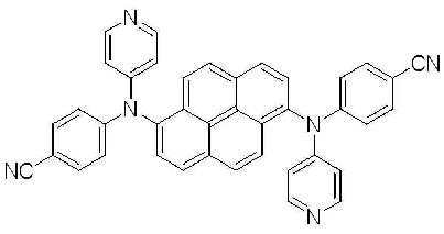
2구 둥근 바닥 플라스크에 상기 실시예 1-(1)에서 제조된 1,6-디브로모피렌 (6.9 g, 0.019 mol), 상기 실시예 1-(2)에서 얻어진 4-시아노페닐 페닐아민 (8.9 g, 0.046 mol), BINAP (0.48 g, 1% mol), Pd(OAc)2 (0.13 g, 1%mol) 및 NaOtBu (6.4 g, 0.07 mol)를 톨루엔 (400 mL)에 녹인후 24시간 동안 환류시켰다. 상기 반응이 종결된 후, 뜨거운 상태에서 여과한 뒤 깔대기 위의 고체를 MC로 세척한 후 용매를 제거하고 MC를 전개용매로 사용하여 컬럼크로마토그래피로 분리한 다음, 메탄올로 재결정하여 노란색의 고체 1.5g을 얻었다. 1,6-dibromopyrene (6.9 g, 0.019 mol) prepared in Example 1- (1) in a two-neck round bottom flask, 4-cyanophenyl phenylamine obtained in Example 1- (2) (8.9 g, 0.046 mol), BINAP (0.48 g, 1% mol), Pd (OAc) 2 (0.13 g, 1% mol) and NaO t Bu (6.4 g, 0.07 mol) were dissolved in toluene (400 mL) It was then refluxed for 24 hours. After the reaction was completed, the mixture was filtered in a hot state, washed with solid MC on the funnel, and then the solvent was removed, and then separated by column chromatography using MC as a developing solvent, and then recrystallized with methanol to give a yellow solid 1.5. g was obtained.
m.p.353.31℃, m.p. 353.31 ° C.,
λABS max : 408nm λFlu max : 453nm, λ ABS max : 408nm λ Flu max : 453 nm,
1H NMR (500 MHz, CDCl3) δ8.19 (d, 2H, J=9 Hz), 8.09 (d, 2H, J=9 Hz), 8.11 (d, 2H, J=9 Hz), 7.85 (d, 2H, J=9 Hz), 7.40 (d, 4H, J=9 Hz), 7.31 (t, 4H, J=8 Hz), 7.26 (d, 4H, J=9 Hz), 7.14 (t, 2H, J=8 Hz), 6.88 (d, 4H, J=9 Hz)) 1 H NMR (500 MHz, CDCl 3 ) δ8.19 (d, 2H, J = 9 Hz), 8.09 (d, 2H, J = 9 Hz), 8.11 (d, 2H, J = 9 Hz), 7.85 ( d, 2H, J = 9 Hz), 7.40 (d, 4H, J = 9 Hz), 7.31 (t, 4H, J = 8 Hz), 7.26 (d, 4H, J = 9 Hz), 7.14 (t, 2H, J = 8 Hz), 6.88 (d, 4H, J = 9 Hz))
1-(4) 1- (4) 유기전계발광소자의Of organic light emitting device 제조 Produce
ITO 글래스의 발광 면적이 3mm X 3mm 크기가 되도록 패터닝한 후 세정하고 진공 챔버에 장착한 다음, 압력이 1X10⁻⁶torr가 되도록 한 후 유기물을 상기 ITO 글래스위에 CuPC (650Å), NPD(400Å), 상기 실시예 1-(3)에서 제조된 BD1(5%) + BH-1(200Å), Alq3(350Å), LiF(5Å), Al(1000Å)의 순서로 성막하여 유기전계발광소자를 제조하였다. After patterning the luminous area of the ITO glass so that it is 3 mm x 3 mm in size, it is cleaned, mounted in a vacuum chamber, the pressure is 1X10 -6 torr, and then the organic material is deposited on the ITO glass, CuPC (650 kPa), NPD (400 kPa), An organic light emitting display device was manufactured by forming a film in a sequence of BD1 (5%) + BH-1 (200kV), Alq3 (350kV), LiF (5kV), and Al (1000kV) prepared in Example 1- (3). .
실시예 2Example 2
2-(1) 4-2- (1) 4- 시아노페닐Cyanophenyl 나프틸아민(4-cyanophenyl naphtylamine)의Of naphthylamine (4-cyanophenyl naphtylamine) 합성 synthesis
2구 둥근 바닥 플라스크에 4-브로모시아노벤젠 (15.3 g, 0.08 mol), 1-나프틸아민 (12.0 g, 0.08 mol), BINAP (0.7 g, 1% mol), Pd(OAc)2 (0.5 g, 2% mol) 및 NaOtBu (21.3 g, 0.22 mol)를 톨루엔 (300 mL)에 녹인후 24시간 환류시켰다. 상기 반응이 종결된 후, 뜨거운 상태에서 여과한 다음 깔대기 위의 고체를 MC로 세척하 고 여액을 받아 톨루엔을 제거한 후 물과 MC를 사용하여 추출하였다. 다음으로, 유기층의 물을 MgSO4로 제거하고 Hx:EA (10:1)을 전개용매로 사용하여 컬럼크로마토그래피로 분리하였다.4-bromocyanobenzene (15.3 g, 0.08 mol), 1-naphthylamine (12.0 g, 0.08 mol), BINAP (0.7 g, 1% mol), Pd (OAc) 2 (0.5) g, 2% mol) and NaO t Bu (21.3 g, 0.22 mol) were dissolved in toluene (300 mL) and refluxed for 24 hours. After the reaction was terminated, the filtrate was filtered in a hot state, the solid on the funnel was washed with MC and the filtrate was removed toluene and extracted with water and MC. Next, water of the organic layer was removed with MgSO 4 and separated by column chromatography using Hx: EA (10: 1) as a developing solvent.
2-(2) N, N' - 비스 (4- 시아노페닐 )-N, N' - 디나프틸피렌 -1,6-디아민(N, N' - Bis (4-cyanophenyl)-N,N'-dinaphtylpyrene-1,6-diamine)의 합성 (BD2) 2- (2) N, N ' - bis (4-cyanophenyl) -N, N' - di-naphthyl pyrene-1,6-diamine (N, N '- Bis (4-cyanophenyl) -N, N '-dinaphtylpyrene-1,6-diamine) synthesis (BD2)
2구 둥근 바닥 플라스크에 상기 실시예 1-(1)에서 제조된 1,6-디브로모피렌 (3.9 g, 0.011 mol), 상기 실시예 2-(1)에서 얻어진 4-시아노페닐 나프틸아민 (6.4 g, 0.026 mol), BINAP (0.3 g, 4% mol), Pd(OAc)2 (0.1 g, 4%mol) 및 NaOtBu (6.4 g, 0.07 mol)를 톨루엔 (180 mL)에 녹인후 24시간 동안 환류시켰다. 상기 반응이 종결된 후, 뜨거운 상태에서 여과한 뒤 깔대기 위의 고체를 MC로 세척한 후 용매를 제거하고 MC를 전개용매로 사용하여 컬럼크로마토그래피로 분리한 다음, 에테르로 재결정하여 노란색의 고체 0.5g을 얻었다. 1,6-dibromopyrene (3.9 g, 0.011 mol) prepared in Example 1- (1) in a two-neck round bottom flask, 4-cyanophenyl naphthyl obtained in Example 2- (1) Amine (6.4 g, 0.026 mol), BINAP (0.3 g, 4% mol), Pd (OAc) 2 (0.1 g, 4% mol) and NaO t Bu (6.4 g, 0.07 mol) were added to toluene (180 mL). After thawing, the mixture was refluxed for 24 hours. After completion of the reaction, the filtrate was filtered in a hot state, the solid on the funnel was washed with MC, the solvent was removed, MC was separated by column chromatography using a developing solvent, and recrystallized with ether to give a yellow solid 0.5. g was obtained.
m.p.373.7℃, m.p. 373.7 ° C.,
λABS max : 408nm λFlu max : 450nm, λ ABS max : 408nm λ Flu max : 450nm,
1H NMR (500 MHz, CDCl3) δ8.18 (d, 2H, J=9 Hz), 8.12 (d, 2H, J=8 Hz), 8.07 (d, 2H, J=9 Hz), 7.98 (m, 4H), 7.89 (d, 2H, J=9 Hz), 7.83 (t, 2H, 6Hz), 7.55 (t, 2H, J=8 Hz), 7.50 (m, 2H), 7.42 (d, 4H, J=6 Hz), 7.38 (d, 4H, J=9 Hz), 6.62 (m, 4H) 1 H NMR (500 MHz, CDCl 3 ) δ8.18 (d, 2H, J = 9 Hz), 8.12 (d, 2H, J = 8 Hz), 8.07 (d, 2H, J = 9 Hz), 7.98 ( m, 4H), 7.89 (d, 2H, J = 9 Hz), 7.83 (t, 2H, 6 Hz), 7.55 (t, 2H, J = 8 Hz), 7.50 (m, 2H), 7.42 (d, 4H , J = 6 Hz), 7.38 (d, 4H, J = 9 Hz), 6.62 (m, 4H)
2-(3) 2- (3) 유기전계발광소자의Of organic light emitting device 제조 Produce
ITO 글래스의 발광 면적이 3mm X 3mm 크기가 되도록 패터닝한 후 세정하고, 진공 챔버에 장착한 다음, 압력이 1X10⁻⁶torr가 되도록 한 후 유기물을 상기 ITO 글래스위에 CuPC (650Å), NPD(400Å), 상기 실시예 2-(2)에서 제조된 BD2(5%) + BH-1(200Å), Alq3(350Å), LiF(5Å), Al(1000Å)의 순서로 성막하여 유기전계발광소자를 제조하였다. After patterning the light emitting area of the ITO glass to a size of 3 mm X 3 mm, washing it, mounting it in a vacuum chamber, and then adjusting the pressure to 1 × 10 -6 torr. , An organic light emitting display device was manufactured by forming a film in the order of BD2 (5%) + BH-1 (200Å), Alq3 (350Å), LiF (5Å), and Al (1000Å) manufactured in Example 2- (2). It was.
실시예 3Example 3
3-(1) 4-3- (1) 4- 시아노페닐Cyanophenyl 비페닐아민(4- Biphenylamine (4- cyanophenylcyanophenyl biphenylaminebiphenylamine )의 합성) Synthesis
2구 둥근 바닥 플라스크에 4-브로모비페닐 (30 g, 0.13 mol), 4-아미노벤조니트릴 (15.2 g, 0.13 mol), BINAP (1.6 g, 2% mol), Pd(OAc)2 (0.6 g, 2% mol) 및 NaOtBu (24.7 g, 0.26 mol)를 톨루엔 (600 mL)에 녹인후 24시간 환류시켰다. 상기 반응이 종결된 후, 뜨거운 상태에서 여과한 다음 깔대기 위의 고체를 MC로 세척하고 여액을 감압증류 후 톨루엔이 소량 남은 상태에서 헥산을 부어 생긴 결정을 여과하여 10.6g의 고체를 얻었다.4-bromobiphenyl (30 g, 0.13 mol), 4-aminobenzonitrile (15.2 g, 0.13 mol), BINAP (1.6 g, 2% mol), Pd (OAc) 2 (0.6 g) in a two- neck round bottom flask , 2% mol) and NaO t Bu (24.7 g, 0.26 mol) were dissolved in toluene (600 mL) and refluxed for 24 hours. After the reaction was terminated, the mixture was filtered in a hot state and the solid on the funnel was washed with MC, and the filtrate was distilled under reduced pressure, and crystals formed by pouring hexane in a small amount of toluene were filtered to obtain 10.6 g of solid.
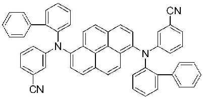
3-(2) N, N' - 비스 (4- 시아노페닐 )-N, N' - 디비페닐피렌 -1,6-디아민(N, N' - Bis (4- cyanophenyl)-N,N'-dibiphenylpyrene-1,6-diamine)의 합성 (BD4) 3- (2) N, N ' - bis (4-cyanophenyl) -N, N' - DB phenyl pyrene-1,6-diamine (N, N '- Bis (4-cyanophenyl) -N, N' -dibiphenylpyrene-1,6-diamine) (BD4)
2구 둥근 바닥 플라스크에 상기 실시예 1-(1)에서 제조된 1,6-디브로모피렌 (5.9 g, 0.016 mol), 상기 실시예 3-(1)에서 얻어진 4-시아노페닐 비페닐아민 (10.6 g, 0.039 mol), BINAP (0.41 g, 4% mol), Pd(OAc)2 (0.1 g, 3% mol) 및 NaOtBu (5.5 g, 0.06 mol)를 톨루엔 (270 mL)에 녹인후 24시간 동안 환류시켰다. 상기 반응이 종결된 후, 뜨거운 상태에서 여과한 뒤 깔대기 위의 고체를 MC로 세척한 후 용매를 제거하고 MC를 전개용매로 사용하여 컬럼크로마토그래피로 분리한 다음, 메탄올로 재결정하여 고체 4.8g을 얻었다. 1,6-dibromopyrene (5.9 g, 0.016 mol) prepared in Example 1- (1) in a two-neck round bottom flask, 4-cyanophenyl biphenyl obtained in Example 3- (1) Amine (10.6 g, 0.039 mol), BINAP (0.41 g, 4% mol), Pd (OAc) 2 (0.1 g, 3% mol) and NaO t Bu (5.5 g, 0.06 mol) were added to toluene (270 mL). After thawing, the mixture was refluxed for 24 hours. After the reaction was terminated, the mixture was filtered in a hot state, washed with solid MC on the funnel, the solvent was removed, and MC was separated by column chromatography using a developing solvent, and then recrystallized with methanol to give 4.8 g of solid. Got it.
m.p.325.9℃, m.p. 325.9 ° C.,
λABS max : 412nm λFlu max : 462nm, λ ABS max : 412nm λ Flu max : 462 nm,
1H NMR (500 MHz, CDCl3) δ8.22 (d, 2H, J=9 Hz), 8.12 (d, 2H, J=9 Hz), 8.05 (d, 2H, J=9 Hz), 7.91 (d, 2H, J=9 Hz), 7.55 (m, 8H), 7.42 (m, 8H), 7.35 (d, 2H, J=9 Hz), 7.30 (m, 4H), 6.95 (d, 4H, J=9 Hz) 1 H NMR (500 MHz, CDCl 3 ) δ8.22 (d, 2H, J = 9 Hz), 8.12 (d, 2H, J = 9 Hz), 8.05 (d, 2H, J = 9 Hz), 7.91 ( d, 2H, J = 9 Hz), 7.55 (m, 8H), 7.42 (m, 8H), 7.35 (d, 2H, J = 9 Hz), 7.30 (m, 4H), 6.95 (d, 4H, J = 9 Hz)
3-(3) 3- (3) 유기전계발광소자의Of organic light emitting device 제조 Produce
ITO 글래스의 발광 면적이 3mm X 3mm 크기가 되도록 패터닝한 후 세정하고, 진공 챔버에 장착한 다음, 압력이 1X10⁻⁶torr가 되도록 한 후 유기물을 상기 ITO 글래스위에 CuPC (650Å), NPD(400Å), 상기 실시예 3-(2)에서 제조된 BD4(5%) + BH- 1(200Å), Alq3(350Å), LiF(5Å), Al(1000Å)의 순서로 성막하여 유기전계발광소자를 제조하였다. After patterning the light emitting area of the ITO glass to a size of 3mm x 3mm, washing it, mounting it in a vacuum chamber, and then adjusting the pressure to 1X10 -6 torr, the organic material was deposited on the ITO glass, CuPC (650Å), NPD (400Å). , An organic light emitting diode was manufactured by forming a film in the order of BD4 (5%) + BH-1 (200kV), Alq3 (350kV), LiF (5kV), and Al (1000kV) prepared in Example 3- (2). It was.
실시예 4Example 4
4-(1) 4- 시아노페닐 -(2-비페닐)아민(4- cyanophenyl -(2- bipheny ) lamine )의 합성 Synthesis of 4- (1) 4- cyanophenyl- (2-biphenyl) amine (4- cyanophenyl- (2- bipheny ) lamine )
2구 둥근 바닥 플라스크에 4-브로모비페닐 (20.2g, 0.087 mol), 4-아미노벤조니트릴 (12.5 g, 0.106 mol), DPPF (2.5 g, 5% mol), Pd(OAc)2 (5 g, 4% mol) 및 NaOtBu (17 g, 0.177 mol)를 톨루엔 (400 mL)에 녹인후 24시간 환류시켰다. 상기 반응이 종결된 후, 뜨거운 상태에서 여과한 다음 깔대기 위의 고체를 MC로 세척하고 용매를 제거한 후 MC를 전개용매로 사용하여 컬럼크로마토그래피로 분리한 뒤 과량의 헥산을 가하여 생긴 결정을 여과하여 11g의 고체를 얻었다.4-bromobiphenyl (20.2 g, 0.087 mol), 4-aminobenzonitrile (12.5 g, 0.106 mol), DPPF (2.5 g, 5% mol), Pd (OAc) 2 (5 g) in a two- neck round bottom flask , 4% mol) and NaO t Bu (17 g, 0.177 mol) were dissolved in toluene (400 mL) and refluxed for 24 hours. After the reaction was completed, the mixture was filtered in a hot state, washed with MC on the funnel, the solvent was removed, MC was separated by column chromatography using a developing solvent, and the crystals formed by adding excess hexane were filtered. 11 g of solid was obtained.
4-(2) N, N' - 비스 (4- 시아노페닐 )-N, N' - 디(2-비페닐)피렌 -1,6- 디아민 (N, N' -Bis (4-cyanophenyl)-N,N'-di(2-biphenyl)pyrene-1,6-diamine)의 합성 (BD5) 4- (2) N, N' - bis (4- cyanophenyl ) -N, N' - di (2-biphenyl) pyrene- 1,6- diamine (N, N' - Bis (4-cyanophenyl) Synthesis of -N, N'-di (2-biphenyl) pyrene-1,6-diamine) (BD5)
2구 둥근 바닥 플라스크에 상기 실시예 1-(1)에서 제조된 1,6-디브로모피렌 (9.85 g, 0.027 mol), 상기 실시예 4-(1)에서 얻어진 4-시아노페닐-(2-비페닐)아민 (14.8 g, 0.055 mol), BINAP (0.68 g, 4% mol), Pd(OAc)2 (0.25 g, 4% mol) 및 NaOtBu (10.6 g, 0.11 mol)를 톨루엔 (450 mL)에 녹인후 24시간 동안 환류시켰다. 상기 반응이 종결된 후, 뜨거운 상태에서 여과한 뒤 깔대기 위의 고체를 MC로 세척한 후 용매를 제거하고 MC를 전개용매로 사용하여 컬럼크로마토그래피로 분리한 다음, 헥산으로 재결정하여 고체 1.3g을 얻었다. 1,6-dibromopyrene (9.85 g, 0.027 mol) prepared in Example 1- (1) in a two-neck round bottom flask, 4-cyanophenyl- (obtained in Example 4- (1) 2-biphenyl) amine (14.8 g, 0.055 mol), BINAP (0.68 g, 4% mol), Pd (OAc) 2 (0.25 g, 4% mol) and NaO t Bu (10.6 g, 0.11 mol) It was dissolved in (450 mL) and refluxed for 24 hours. After the reaction was terminated, the mixture was filtered in a hot state, washed with solid MC on the funnel, the solvent was removed, and MC was separated by column chromatography using a developing solvent, and then recrystallized with hexane to give 1.3 g of solid. Got it.
m.p.335.84℃, m.p. 335.84 ° C.,
λABS max : 418nm λFlu max : 453nm, λ ABS max : 418nm λ Flu max : 453 nm,
1H NMR (500 MHz, CDCl3) δ7.93 (d, 2H, J=8 Hz), 7.65 (d, 2H, J=9 Hz), 7.58 (d, 2H, J=8 Hz), 7.55 (d, 2H, J=9 Hz), 7.42 (m, 4H), 7.35 (m, 4H), 7.25(m, 6H), 7.08 (d, 6H, J=6 Hz), 6.90 (d, 6H, J=6 Hz) 1 H NMR (500 MHz, CDCl 3 ) δ7.93 (d, 2H, J = 8 Hz), 7.65 (d, 2H, J = 9 Hz), 7.58 (d, 2H, J = 8 Hz), 7.55 ( d, 2H, J = 9 Hz), 7.42 (m, 4H), 7.35 (m, 4H), 7.25 (m, 6H), 7.08 (d, 6H, J = 6 Hz), 6.90 (d, 6H, J = 6 Hz)
4-(3) 4- (3) 유기전계발광소자의Of organic light emitting device 제조 Produce
ITO 글래스의 발광 면적이 3mm X 3mm 크기가 되도록 패터닝한 후 세정하고, 진공 챔버에 장착한 다음, 압력이 1X10⁻⁶torr가 되도록 한 후 유기물을 상기 ITO 글래스위에 CuPC (650Å), NPD(400Å), 상기 실시예 4-(2)에서 제조된 BD5(5%) + BH-1(200Å), Alq3(350Å), LiF(5Å), Al(1000Å)의 순서로 성막하여 유기전계발광소자를 제조하였다.After patterning the light emitting area of the ITO glass to a size of 3 mm X 3 mm, washing it, mounting it in a vacuum chamber, and then adjusting the pressure to 1 × 10 -6 torr. , An organic light emitting diode was manufactured by forming a film in the order of BD5 (5%) + BH-1 (200kV), Alq3 (350kV), LiF (5kV), and Al (1000kV) prepared in Example 4- (2). It was.
실시예 5 Example 5
5-(1) 4-5- (1) 4- 시아노페닐Cyanophenyl -(2--(2- 메틸페닐Methylphenyl )아민(4-) Amine (4- cyanophenylcyanophenyl -(2--(2- methylphenymethylpheny ))
laminelamine )의 합성) Synthesis
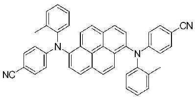
2구 둥근 바닥 플라스크에 4-브로모벤조니트릴 (30g, 0.165 mol), o-톨루이딘 (17.7 g, 0.1653 mol), BINAP (4.1 g, 4% mol), Pd(OAc)2 (0.7 g, 2% mol) 및 NaOtBu (31.7 g, 0.33 mol)를 톨루엔 (400 mL)에 녹인후 24시간 환류시켰다. 상기 반응이 종결된 후, 뜨거운 상태에서 여과한 다음 깔대기 위의 고체를 MC로 세척하고 용매를 제거한 후 MC를 전개용매로 사용하여 컬럼크로마토그래피로 분리한 뒤 과량의 헥산을 가하여 생긴 결정을 여과하여 7.9g의 고체를 얻었다.4-bromobenzonitrile (30 g, 0.165 mol), o-toluidine (17.7 g, 0.1653 mol), BINAP (4.1 g, 4% mol), Pd (OAc) 2 (0.7 g, 2) in a two -neck round bottom flask % mol) and NaO t Bu (31.7 g, 0.33 mol) were dissolved in toluene (400 mL) and refluxed for 24 hours. After the reaction was completed, the mixture was filtered in a hot state, washed with MC on the funnel, the solvent was removed, MC was separated by column chromatography using a developing solvent, and the crystals formed by adding excess hexane were filtered. 7.9 g of solid were obtained.
5-(2) N, N' - 비스 (4- 시아노페닐 )-N, N' - 비스(2-메틸페닐)피렌 -1,6- 디아민 (N,N'-Bis (4-cyanophenyl)-N,N'-bis(2-methylphenyl)pyrene-1,6-diamine)의 합성 (BD7) 5- (2) N, N' - bis (4- cyanophenyl ) -N, N' - bis (2-methylphenyl) pyrene- 1,6- diamine Synthesis of (N, N'-Bis (4-cyanophenyl) -N, N'-bis (2-methylphenyl) pyrene-1,6-diamine) (BD7)
2구 둥근 바닥 플라스크에 상기 실시예 1-(1)에서 제조된 1,6-디브로모피렌 (5.7 g, 0.016 mol), 상기 실시예 5-(1)에서 얻어진 4-시아노페닐-(2-메틸페닐)아민 (7.9 g, 0.038 mol), BINAP (0.39 g, 1% mol), Pd(OAc)2 (0.11 g, 3% mol) 및 NaOtBu (5.3 g, 0.06 mol)를 톨루엔 (260 mL)에 녹인후 24시간 동안 환류시켰다. 상기 반응이 종결된 후, 뜨거운 상태에서 여과한 뒤 깔대기 위의 고체를 MC로 세척한 후 용매를 제거하고 소량의 MC를 첨가한 다음, 에테르를 첨가하고 결정을 여과하여 연두색 고체 1.7g을 얻었다. In a two-neck round bottom flask, 1,6-dibromopyrene (5.7 g, 0.016 mol) prepared in Example 1- (1), 4-cyanophenyl- (obtained in Example 5- (1) 2-methylphenyl) amine (7.9 g, 0.038 mol), BINAP (0.39 g, 1% mol), Pd (OAc) 2 (0.11 g, 3% mol) and NaO t Bu (5.3 g, 0.06 mol) were added to toluene ( 260 mL) and refluxed for 24 hours. After the reaction was terminated, the mixture was filtered in a hot state and the solid on the funnel was washed with MC, the solvent was removed, a small amount of MC was added, ether was added, and the crystals were filtered to obtain 1.7 g of a light green solid.
m.p.373.1℃, m.p. 373.1 ° C.,
λABS max : 408nm λFlu max : 450nm, λ ABS max : 408nm λ Flu max : 450nm,
1H NMR (500 MHz, CDCl3) δ8.12 (d, 2H, J=8 Hz), 8.0 (d, 2H, J=8 Hz), 7.98 (d, 2H, J=8 Hz), 7.72 (d, 2H, J=8 Hz), 7.38 (d, 4H, J=8 Hz), 7.34 (d, 4H, J= 8 Hz), 7.20 (m, 6H), 6.60 (m, 4H), 2.20 (s, 6H) 1 H NMR (500 MHz, CDCl 3 ) δ8.12 (d, 2H, J = 8 Hz), 8.0 (d, 2H, J = 8 Hz), 7.98 (d, 2H, J = 8 Hz), 7.72 ( d, 2H, J = 8 Hz), 7.38 (d, 4H, J = 8 Hz), 7.34 (d, 4H, J = 8 Hz), 7.20 (m, 6H), 6.60 (m, 4H), 2.20 ( s, 6 H)
5-(3) 5- (3) 유기전계발광소자의Of organic light emitting device 제조 Produce
ITO 글래스의 발광 면적이 3mm X 3mm 크기가 되도록 패터닝한 후 세정하고, 진공 챔버에 장착한 다음, 압력이 1X10⁻⁶torr가 되도록 한 후 유기물을 상기 ITO 글래스위에 CuPC (650Å), NPD(400Å), 상기 실시예 5-(2)에서 제조된 BD7(5%) + BH-1(200Å), Alq3(350Å), LiF(5Å), Al(1000Å)의 순서로 성막하여 유기전계발광소자를 제조하였다.After patterning the light emitting area of the ITO glass to a size of 3mm x 3mm, washing it, mounting it in a vacuum chamber, and then adjusting the pressure to 1X10 -6 torr, the organic material was deposited on the ITO glass, CuPC (650Å), NPD (400Å). , An organic light emitting diode was manufactured by forming a film in the order of BD7 (5%) + BH-1 (200kV), Alq3 (350kV), LiF (5kV), and Al (1000kV) prepared in Example 5- (2). It was.
실시예 6Example 6
6-(1) 4-6- (1) 4- 시아노페닐Cyanophenyl -4-t-부틸페닐아민(4-4-t-butylphenylamine (4- cyanophenylcyanophenyl -4-t--4-t- buthylphenylbuthylphenyl
amineamine )의 합성) Synthesis
2구 둥근 바닥 플라스크에 4-브로모벤조니트릴 (15g, 0.08 mol), 4-t-부틸벤젠 (12.3 g, 0.08 mol), BINAP (1 g, 2% mol), Pd(OAc)2 (0.4 g, 2% mol) 및 NaOtBu (15.8 g, 0.16 mol)를 톨루엔 (300 mL)에 녹인후 24시간 환류시켰다. 상기 반응이 종결된 후, 뜨거운 상태에서 여과한 다음 깔대기 위의 고체를 MC로 세척하고 용매를 감압증류하여 제거한 뒤 MC와 물로 추출하고 유기층을 분리하였다. 마지막으로 상기 유기층의 물을 MgSO4로 제거한 후 MC를 전개용매로 사용하여 컬럼크로마토그래피로 분리한 뒤 메탄올로 재결정하여 5.5g의 고체를 얻었다.4-bromobenzonitrile (15 g, 0.08 mol), 4-t-butylbenzene (12.3 g, 0.08 mol), BINAP (1 g, 2% mol), Pd (OAc) 2 (0.4 in a two -neck round bottom flask g, 2% mol) and NaO t Bu (15.8 g, 0.16 mol) were dissolved in toluene (300 mL) and refluxed for 24 hours. After the reaction was terminated, the mixture was filtered in a hot state and the solid on the funnel was washed with MC, the solvent was distilled off under reduced pressure, extracted with MC and water, and the organic layer was separated. Finally, water of the organic layer was removed with MgSO 4 , MC was separated by column chromatography using a developing solvent, and recrystallized with methanol to obtain 5.5 g of solid.
6-(2) N, N' - 비스 (4- 시아노페닐 )-N, N' - 비스(4-t-부틸페닐)피렌 -1,6- 디아민 (N,N'-Bis (4-cyanophenyl)-N,N'-bis(4-t-buthylphenyl)pyrene-1,6-diamine)의 합성 (BD9) 6- (2) N, N' - bis (4- cyanophenyl ) -N, N' - bis (4-t-butylphenyl) pyrene- 1,6- diamine Synthesis of (N, N'-Bis (4-cyanophenyl) -N, N'-bis (4-t-buthylphenyl) pyrene-1,6-diamine) (BD9)
2구 둥근 바닥 플라스크에 상기 실시예 1-(1)에서 제조된 1,6-디브로모피렌 (3.3 g, 0.009 mol), 상기 실시예 6-(1)에서 얻어진 4-시아노페닐-4-t-부틸페닐아민 (5.5 g, 0.022 mol), BINAP (0.23 g, 4% mol), Pd(OAc)2 (0.08 g, 4% mol) 및 NaOtBu (3.5 g, 0.06 mol)를 톨루엔 (150 mL)에 녹인후 24시간 동안 환류시켰다. 상기 반응이 종결된 후, 뜨거운 상태에서 여과한 뒤 깔대기 위의 고체를 MC로 세척한 후 용매를 제거하고 소량의 MC를 첨가한 다음, 메탄올을 첨가하여 결정을 얻었다. 다음으로, MC를 전개용매로 사용하여 컬럼크로마토그래피로 분리한 후 에테르로 재결정하여 고체 1.7g을 얻었다. 1,6-dibromopyrene (3.3 g, 0.009 mol) prepared in Example 1- (1) in a two-neck round bottom flask, 4-cyanophenyl-4 obtained in Example 6- (1) -t-butylphenylamine (5.5 g, 0.022 mol), BINAP (0.23 g, 4% mol), Pd (OAc) 2 (0.08 g, 4% mol) and NaO t Bu (3.5 g, 0.06 mol) toluene It was dissolved in (150 mL) and refluxed for 24 hours. After the reaction was terminated, the mixture was filtered in a hot state, the solid on the funnel was washed with MC, the solvent was removed, a small amount of MC was added, and methanol was added to obtain crystals. Next, using MC as a developing solvent and separated by column chromatography and recrystallized with ether to give a 1.7g of a solid.
m.p.425.1℃, m.p. 425.1 ° C.,
λABS max : 410nm λFlu max : 461nm, λ ABS max : 410nm λ Flu max : 461 nm,
1H NMR (500 MHz, CDCl3) δ8.22 (d, 2H, J=8 Hz), 8.12 (d, 2H, J=9 Hz), 8.05 (d, 2H, J=9 Hz), 7.90 (d, 2H, J=8 Hz), 7.42 (d, 2H, J=8 Hz), 7.35 (d, 4H, J=8 Hz), 7.22 (d, 4H, J=8 Hz), 6.88 (d, 4H, J=8 Hz), 1.30 (s, 18H) 1 H NMR (500 MHz, CDCl 3 ) δ8.22 (d, 2H, J = 8 Hz), 8.12 (d, 2H, J = 9 Hz), 8.05 (d, 2H, J = 9 Hz), 7.90 ( d, 2H, J = 8 Hz), 7.42 (d, 2H, J = 8 Hz), 7.35 (d, 4H, J = 8 Hz), 7.22 (d, 4H, J = 8 Hz), 6.88 (d, 4H, J = 8 Hz), 1.30 (s, 18H)
6-(3) 6- (3) 유기전계발광소자의Of organic light emitting device 제조 Produce
ITO 글래스의 발광 면적이 3mm X 3mm 크기가 되도록 패터닝한 후 세정하고, 진공 챔버에 장착한 다음, 압력이 1X10⁻⁶torr가 되도록 한 후 유기물을 상기 ITO 글래스위에 CuPC (650Å), NPD(400Å), 상기 실시예 6-(2)에서 제조된 BD9(5%) + BH-1(200Å), Alq3(350Å), LiF(5Å), Al(1000Å)의 순서로 성막하여 유기전계발광소자를 제조하였다.After patterning the light emitting area of the ITO glass to a size of 3mm x 3mm, washing it, mounting it in a vacuum chamber, and then adjusting the pressure to 1X10 -6 torr, the organic material was deposited on the ITO glass, CuPC (650Å), NPD (400Å). , An organic light emitting display device was manufactured by forming a film of BD9 (5%) + BH-1 (200kV), Alq3 (350kV), LiF (5kV), and Al (1000kV) in the order of Example 6- (2). It was.
실시예 7Example 7
7-(1) 4-브로모페닐트리메틸실란(4-7- (1) 4-bromophenyltrimethylsilane (4- bromophenyltrimethylsilanebromophenyltrimethylsilane )의 합성) Synthesis
3구 둥근 바닥 플라스크에 1,4-디브로모벤젠 (12.7 g, 0.053 mol)과 디에틸에테르(300ml)를 넣고 용해시킨 다음, 플라스크의 외부온도를 -78℃로 냉각시키고 n-BuLi을 천천히 적가시켰다. 다음으로 온도를 0℃로 1시간에 걸쳐 승온하고 클로로트리메틸실란(7.51ml, 0.059mol)을 천천히 적가하고 다시 온도를 상온으로 승온하였다. 반응이 종결된 후 물과 디에틸에테르를 사용하여 추출하고 MgSO4로 물을 제 거한 다음 용매를 제거하고 감압하에서 분별증류하여 4-브로모페닐트리메틸실란 (11.3 g, 92 %) 을 얻었다.Dissolve 1,4-dibromobenzene (12.7 g, 0.053 mol) and diethyl ether (300 ml) in a three-neck round bottom flask, cool the flask to -78 ° C and slowly n-BuLi I dropped it. Next, the temperature was raised to 0 ° C. over 1 hour, and chlorotrimethylsilane (7.51 ml, 0.059 mol) was slowly added dropwise, and the temperature was again raised to room temperature. After completion of the reaction, the mixture was extracted with water and diethyl ether, water was removed with MgSO 4 , and then the solvent was removed and fractional distillation was performed under reduced pressure to obtain 4-bromophenyltrimethylsilane (11.3 g, 92%).
7-(2)4- 시아노페닐 -4-트리메틸실리페닐아민(4- cyanophenyl -4-trimethyl silylphenylamine)의 합성 7- (2) Synthesis of 4-cyano-4-trimethylsilyoxy phenylamine (4-cyanophenyl-4-trimethyl silylphenylamine)
2구 둥근 바닥 플라스크에 상기 실시예 1-(2)에서 제조된 4-시아노페닐 페닐아민 (1.2ml, 0.0076 mol), 상기 실시예 7-(1)에서 제조된 4-브로모페닐트리메틸실란 (1 g, 0.0044 mol), BINAP (0.03 g, 1% mol), Pd(OAc)2 (0.01 g, 1% mol) 및 NaOtBu (1.5 g, 0.016 mol)를 톨루엔 (50 mL)에 녹인후 24시간 환류시켰다. 상기 반응이 종결된 후, 플라스크를 냉각시키고 반응용액인 톨루엔을 제거한 다음 헥산을 사용하여 컬럼 분리를 하고 에탄올과 물을 사용하여 침전이 생기면 이것을 여과하여 흰색 고체인 4-시아노페닐-4-트리메틸실릴페닐아민(1.12g, 86%)을 얻었다.4-cyanophenyl phenylamine (1.2 ml, 0.0076 mol) prepared in Example 1- (2), 4-bromophenyltrimethylsilane prepared in Example 7- (1) in a two-neck round bottom flask (1 g, 0.0044 mol), BINAP (0.03 g, 1% mol), Pd (OAc) 2 (0.01 g, 1% mol) and NaO t Bu (1.5 g, 0.016 mol) dissolved in toluene (50 mL) It was refluxed for 24 hours. After the reaction was completed, the flask was cooled, the reaction solution toluene was removed, and the column was separated using hexane, and then precipitated using ethanol and water. The precipitate was filtered to give 4-cyanophenyl-4-trimethyl as a white solid. Silylphenylamine (1.12 g, 86%) was obtained.
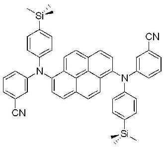
7-(3)N, N' - 비스 (4- 시아노페닐 )-N, N' - 비스(4-트리메틸실릴페닐)피렌 -1,6- 디아민 (N,N'-Bis (4-cyanophenyl)-N,N'-bis(4-trimethylsilylphenyl) pyrene-1,6-diamine)의 합성 (BD17) 7- (3) N, N' - bis (4- cyanophenyl ) -N, N' - bis (4-trimethylsilylphenyl) pyrene- 1,6 - diamine (N, N'-Bis (4- cyanophenyl) -N, N'-bis (4-trimethylsilylphenyl) pyrene-1,6-diamine) (BD17)
2구 둥근 바닥 플라스크에 상기 실시예 1-(1)에서 제조된 1,6-디브로모피렌 (3.9 g, 0.011 mol), 상기 실시예 7-(2)에서 얻어진 4-시아노페닐-4-트리메틸실릴페닐아민 (6.9 g, 0.026 mol), BINAP (0.27 g, 4% mol), Pd(OAc)2 (0.10 g, 4% mol) 및 NaOtBu (4.2 g, 0.04 mol)를 톨루엔 (50 mL)에 녹인후 24시간 동안 환류시켰다. 상기 반응이 종결된 후, 뜨거운 상태에서 여과한 뒤 깔대기 위의 고체를 MC로 세척하였다. 상기 MC 및 톨루엔을 감압하여 제거한 다음 메탄올을 첨가하여 결정을 얻고, 상기 결정을 MC로 컬럼분리하였다. 마지막으로, 상기 MC를 감압하여 제거한 후 소량의 MC에 에테르를 첨가하여 결정을 얻은 다음, MC/MeOH로 재결정하여 2g의 고체를 얻었다. 1,6-dibromopyrene (3.9 g, 0.011 mol) prepared in Example 1- (1) in a two-neck round bottom flask, 4-cyanophenyl-4 obtained in Example 7- (2) -Trimethylsilylphenylamine (6.9 g, 0.026 mol), BINAP (0.27 g, 4% mol), Pd (OAc) 2 (0.10 g, 4% mol) and NaO t Bu (4.2 g, 0.04 mol) were added to toluene ( 50 mL) and refluxed for 24 hours. After the reaction was completed, the solid on the funnel was washed with MC after filtration in hot state. The MC and toluene were removed under reduced pressure, and methanol was added to obtain crystals, and the crystals were column separated with MC. Finally, the MC was removed under reduced pressure, and then ether was added to a small amount of MC to obtain crystals, followed by recrystallization with MC / MeOH to obtain 2 g of solid.
m.p.361.8℃, m.p. 361.8 ° C.,
λABS max : 410nm λFlu max : 456nm, λ ABS max : 410nm λ Flu max : 456 nm,
1H NMR (500 MHz, CDCl3) δ8.18 (d, 2H, J=8 Hz), 8.08 (d, 2H, J=9 Hz), 8.0 (d, 2H, J=9 Hz), 7.42 (d, 4H, J=9 Hz), 7.40 (d, 4H, J=9 Hz), 7.20 (d, 4H, J=9 Hz), 6.92 (d, 4H, J=9 Hz), 0.25(s, 18H) 1 H NMR (500 MHz, CDCl 3 ) δ8.18 (d, 2H, J = 8 Hz), 8.08 (d, 2H, J = 9 Hz), 8.0 (d, 2H, J = 9 Hz), 7.42 ( d, 4H, J = 9 Hz), 7.40 (d, 4H, J = 9 Hz), 7.20 (d, 4H, J = 9 Hz), 6.92 (d, 4H, J = 9 Hz), 0.25 (s, 18H)
7-(4) 7- (4) 유기전계발광소자의Of organic light emitting device 제조 Produce
ITO 글래스의 발광 면적이 3mm X 3mm 크기가 되도록 패터닝한 후 세정하고, 진공 챔버에 장착한 다음, 압력이 1X10⁻⁶torr가 되도록 한 후 유기물을 상기 ITO 글래스위에 CuPC (650Å), NPD(400Å), 상기 실시예 7-(3)에서 제조된 BD17(5%) + BH-1(200Å), Alq3(350Å), LiF(5Å), Al(1000Å)의 순서로 성막하여 유기전계발광소자를 제조하였다.After patterning the light emitting area of the ITO glass to a size of 3 mm X 3 mm, washing it, mounting it in a vacuum chamber, and then adjusting the pressure to 1 × 10 -6 torr. , An organic light emitting diode was manufactured by forming a film of BD17 (5%) + BH-1 (200kV), Alq3 (350kV), LiF (5kV), and Al (1000kV) in the order of Example 7- (3). It was.
실시예 8Example 8
8-(1) 디-4-8- (1) Di-4- 시아노페닐아민(di-4-cyanophenylamine)의Of di-4-cyanophenylamine 합성 synthesis
2구 둥근 바닥 플라스크에 4-브로모벤조니트릴 (30g, 0.16 mol), 4-아미노벤조니트릴 (19.5 g, 0.16 mol), BINAP (2.0 g, 2% mol), Pd(OAc)2 (0.9 g, 2% mol) 및 NaOtBu (31.7 g, 0.33 mol)를 톨루엔 (600 mL)에 녹인후 24시간 환류시켰다. 상기 반응이 종결된 후, 뜨거운 상태에서 여과한 다음 깔대기 위의 고체를 MC로 세척하고 용매를 제거한 후 MC 및 과량의 메탄올로 세척하고 얻은 용액을 감압하여 용매를 제거한 다음, 톨루엔을 소량 첨가한 후 헥산을 부어 재결정하여 베이지색의 고체 16.7g을 얻었다.4-bromobenzonitrile (30 g, 0.16 mol), 4-aminobenzonitrile (19.5 g, 0.16 mol), BINAP (2.0 g, 2% mol), Pd (OAc) 2 (0.9 g) in a two -necked round bottom flask , 2% mol) and NaO t Bu (31.7 g, 0.33 mol) were dissolved in toluene (600 mL) and refluxed for 24 hours. After the reaction was completed, the mixture was filtered under hot state, washed with solid MC on the funnel, the solvent was removed, the MC was washed with excess methanol, and the resulting solution was removed under reduced pressure to remove the solvent, and then a small amount of toluene was added. Hexane was poured and recrystallized to give 16.7 g of a beige solid.
8-(2)N,N, N' , N' - 테트라시아노페닐피렌 -1,6-디아민(N,N, N' , N' -Tetracyano phenylpyrene-1,6-diamine)의 합성 (BD19) Synthesis of 8- (2) N, N, N ' , N' - tetracyanophenylpyrene- 1,6-diamine (N, N, N' , N' - Tetracyano phenylpyrene-1,6-diamine) (BD19 )
2구 둥근 바닥 플라스크에 상기 실시예 1-(1)에서 제조된 1,6-디브로모피렌 (5.0 g, 0.014 mol), 상기 실시예 8-(1)에서 얻어진 디-4-시아노페닐아민 (7.3 g, 0.033 mol), BINAP (1.73 g, 2% mol), Pd(OAc)2 (0.16 g, 1% mol) 및 NaOtBu (5.3 g, 0.06 mol)를 톨루엔 (50 mL)에 녹인후 24시간 동안 환류시켰다. 상기 반응이 종결된 후, 뜨거운 상태에서 여과한 뒤 깔대기 위의 고체를 MC로 세척한 후 용매를 제거하고 메탄올을 첨가하여 결정을 얻었다. 다음으로 상기 고체를 MC를 전개용매로 사용하여 컬럼크로마토그래피로 분리하고, MC를 감압하여 제거한 후 소량의 MC 에 에테르를 첨가하여 0.2g의 고체를 얻었다. 1,6-dibromopyrene (5.0 g, 0.014 mol) prepared in Example 1- (1) in a two-neck round bottom flask, di-4-cyanophenyl obtained in Example 8- (1) Amine (7.3 g, 0.033 mol), BINAP (1.73 g, 2% mol), Pd (OAc) 2 (0.16 g, 1% mol) and NaO t Bu (5.3 g, 0.06 mol) were added to toluene (50 mL). After thawing, the mixture was refluxed for 24 hours. After the reaction was terminated, the mixture was filtered in a hot state and the solid on the funnel was washed with MC and then the solvent was removed and methanol was added to obtain crystals. Next, the solid was separated by column chromatography using MC as a developing solvent, MC was removed under reduced pressure, and a small amount of MC was added to ether to obtain 0.2 g of solid.
m.p.417.4℃, m.p. 417.4 ° C.,
λABS max : 390nm λFlu max : 441nm, λ ABS max : 390nm λ Flu max : 441 nm,
1H NMR (500 MHz, CDCl3) δ8.25 (d, 2H, J=8 Hz), 8.05 (d, 2H, J=9 Hz), 7.95 (d, 2H, J=9 Hz), 7.85 (d, 2H, J=8 Hz), 7.52 (d, 8H, J=8 Hz), 7.12 (d, 8H, J=8 Hz) 1 H NMR (500 MHz, CDCl 3 ) δ8.25 (d, 2H, J = 8 Hz), 8.05 (d, 2H, J = 9 Hz), 7.95 (d, 2H, J = 9 Hz), 7.85 ( d, 2H, J = 8 Hz), 7.52 (d, 8H, J = 8 Hz), 7.12 (d, 8H, J = 8 Hz)
8-(3) 8- (3) 유기전계발광소자의Of organic light emitting device 제조 Produce
ITO 글래스의 발광 면적이 3mm X 3mm 크기가 되도록 패터닝한 후 세정하고, 진공 챔버에 장착한 다음, 압력이 1X10⁻⁶torr가 되도록 한 후 유기물을 상기 ITO 글래스위에 CuPC (650Å), NPD(400Å), 상기 실시예 8-(2)에서 제조된 BD19(5%) + BH-1(200Å), Alq3(350Å), LiF(5Å), Al(1000Å)의 순서로 성막하여 유기전계발광소자를 제조하였다.After patterning the light emitting area of the ITO glass to a size of 3 mm X 3 mm, washing it, mounting it in a vacuum chamber, and then adjusting the pressure to 1 × 10 -6 torr. In Example 8- (2), the BD19 (5%) + BH-1 (200 H), Alq3 (350 Å), LiF (5 Å), Al (1000 Å) to form a film in order to manufacture an organic light emitting device It was.
실시예 9Example 9
9-(1)3- 시아노페닐 -4-트리메틸실릴페닐아민(3- cyanophenyl -4-trimethylsilylphenylamine)의 합성 9 (1) Synthesis of 3-cyano-4-trimethylsilyl-phenyl amine (3-cyanophenyl-4-trimethylsilylphenylamine)
2구 둥근 바닥 플라스크에 3-시아노페닐아민 (1.2ml, 0.0076 mol), 상기 실 시예 7-(1)에서 제조된 4-브로모페닐트리메틸실란 (1 g, 0.0044 mol), BINAP (0.03 g, 1% mol), Pd(OAc)2 (0.01 g, 1% mol) 및 NaOtBu (1.5 g, 0.016 mol)를 톨루엔 (50 mL)에 녹인후 24시간 환류시켰다. 상기 반응이 종결된 후, 플라스크를 냉각시키고 반응용액인 톨루엔을 제거한 다음 물과 MC를 사용하여 추출하고 MgSO4로 물을 제거한 다음 MC를 감압으로 제거하였다. 다음으로 헥산을 사용하여 실리카겔 쇼트 컬럼을 거치게 하고 에탄올과 물을 사용하여 침전이 생기면 이를 여과하여 흰색 고체를 얻었다.3-cyanophenylamine (1.2 ml, 0.0076 mol), 4-bromophenyltrimethylsilane (1 g, 0.0044 mol) prepared in Example 7- (1), BINAP (0.03 g) in a two-neck round bottom flask , 1% mol), Pd (OAc) 2 (0.01 g, 1% mol) and NaO t Bu (1.5 g, 0.016 mol) were dissolved in toluene (50 mL) and refluxed for 24 hours. After the reaction was completed, the flask was cooled, the reaction solution toluene was removed, extracted with water and MC, water was removed with MgSO 4 , and MC was removed under reduced pressure. Next, the mixture was subjected to a silica gel short column using hexane, and precipitated using ethanol and water to obtain a white solid.
9-(2)N, N' - 비스 (3- 시아노페닐 )-N, N' - 비스(4-트리메틸실릴페닐)피렌 -1,6- 디아민(N,N'-Bis(3-cyanophenyl)-N,N'-bis(4-trimethylsilylphenyl)pyrene-1,6-diamine)의 합성 (BD39) 9- (2) N, N' - bis (3- cyanophenyl ) -N, N' - bis (4-trimethylsilylphenyl) pyrene- 1,6 - diamine (N, N'-Bis (3- cyanophenyl) -N, N'-bis (4-trimethylsilylphenyl) pyrene-1,6-diamine) (BD39)
2구 둥근 바닥 플라스크에 상기 실시예 1-(1)에서 제조된 1,6-디브로모피렌 (5.0 g, 0.014 mol), 상기 실시예 9-(1)에서 얻어진 3-시아노페닐-4-트리메틸실릴페닐아민 (8.9 g, 0.033 mol), DPPF (0.38 g, 5% mol), Pd(PPh3)4 (0.80 g, 5% mol) 및 NaOtBu (4 g, 0.04 mol)를 톨루엔 (100 mL)에 녹인후 24시간 동안 환류시켰다. 상기 반응이 종결된 후, EA:Hx(1:8)을 전개용매로 사용하여 컬럼크로마토그래피로 분리한 후 메탄올로 재결정하여 1.4g의 고체를 얻었다. 1,6-dibromopyrene (5.0 g, 0.014 mol) prepared in Example 1- (1) in a two-neck round bottom flask, 3-cyanophenyl-4 obtained in Example 9- (1) Trimethylsilylphenylamine (8.9 g, 0.033 mol), DPPF (0.38 g, 5% mol), Pd (PPh 3 ) 4 (0.80 g, 5% mol) and NaO t Bu (4 g, 0.04 mol) It was dissolved in (100 mL) and refluxed for 24 hours. After completion of the reaction, EA: Hx (1: 8) was used as a developing solvent and separated by column chromatography, and recrystallized with methanol to obtain 1.4g of solid.
m.p.282.0℃, m.p. 282.0 ° C.,
λABS max : 412nm λFlu max : 455nm, λ ABS max : 412nm λ Flu max : 455 nm,
1H NMR (500 MHz, CDCl3) δ8.18 (d, 2H, J=8 Hz), 8.08 (d, 2H, J=9 Hz), 7.98 (d, 2H, J=9 Hz), 7.84 (d, 2H, J=8 Hz), 7.42 (d, 4H, J=8 Hz), 7.22 (m, 6H), 7.15 (d, 2H, J=8 Hz), 7.12 (d, 4H, J=8 Hz), 0.25 (s, 18H) 1 H NMR (500 MHz, CDCl 3 ) δ8.18 (d, 2H, J = 8 Hz), 8.08 (d, 2H, J = 9 Hz), 7.98 (d, 2H, J = 9 Hz), 7.84 ( d, 2H, J = 8 Hz), 7.42 (d, 4H, J = 8 Hz), 7.22 (m, 6H), 7.15 (d, 2H, J = 8 Hz), 7.12 (d, 4H, J = 8 Hz), 0.25 (s, 18H)
9-(3) 9- (3) 유기전계발광소자의Of organic light emitting device 제조 Produce
ITO 글래스의 발광 면적이 3mm X 3mm 크기가 되도록 패터닝한 후 세정하고, 진공 챔버에 장착한 다음, 압력이 1X10⁻⁶torr가 되도록 한 후 유기물을 상기 ITO 글래스위에 CuPC (650Å), NPD(400Å), 상기 실시예 9-(2)에서 제조된 BD39(5%) + BH-2(200Å), Alq3(350Å), LiF(5Å), Al(1000Å)의 순서로 성막하여 유기전계발광소자를 제조하였다.After patterning the light emitting area of the ITO glass to a size of 3 mm X 3 mm, washing it, mounting it in a vacuum chamber, and then adjusting the pressure to 1 × 10 -6 torr. , An organic light emitting diode was manufactured by forming a film in the order of BD39 (5%) + BH-2 (200kV), Alq3 (350kV), LiF (5kV), and Al (1000kV) manufactured in Example 9- (2). It was.
비교예 1Comparative Example 1
ITO 글래스의 발광 면적이 3mm X 3mm 크기가 되도록 패터닝한 후 세정하고, 진공 챔버에 장착한 다음, 압력이 1X10⁻⁶torr가 되도록 한 후 유기물을 상기 ITO 글래스위에 CuPC (650Å), NPD(400Å), 하기 화학식 6의 화합물(5%) + BH-2(200Å), Alq3(350Å), LiF(5Å), Al(1000Å)의 순서로 성막하여 유기전계발광소자를 제조하였다.After patterning the light emitting area of the ITO glass to a size of 3 mm X 3 mm, washing it, mounting it in a vacuum chamber, and then adjusting the pressure to 1 × 10 -6 torr. To form an organic light emitting device was formed by the compound of Formula 6 (5%) + BH-2 (200 Å), Alq3 (350 Å), LiF (5 Å), Al (1000 Å) in order.

비교예 2Comparative Example 2
ITO 글래스의 발광 면적이 3mm X 3mm 크기가 되도록 패터닝한 후 세정하고, 진공 챔버에 장착한 다음, 압력이 1X10⁻⁶torr가 되도록 한 후 유기물을 상기 ITO 글래스위에 CuPC (650Å), NPD(400Å), 하기 화학식 7의 화합물(5%) + BH-1(200Å), Alq3(350Å), LiF(5Å), Al(1000Å)의 순서로 성막하여 유기전계발광소자를 제조하였다.After patterning the light emitting area of the ITO glass to a size of 3 mm X 3 mm, washing it, mounting it in a vacuum chamber, and then adjusting the pressure to 1 × 10 -6 torr. , A compound of Formula 7 (5%) + BH-1 (200 Pa), An organic light emitting display device was fabricated by forming Alq 3 (350 kV), LiF (5 kV), and Al (1000 kV) in this order.

시험예 1Test Example 1
실시예 1∼9와 비교예 1∼2에 따라 제조된 유기전계발광소자에 대하여, 전압, 전류, 휘도 및 색좌표를 측정하고 그 결과를 하기 표 1에 나타내었다.For the organic light emitting diodes manufactured according to Examples 1 to 9 and Comparative Examples 1 and 2, voltage, current, brightness, and color coordinates were measured, and the results are shown in Table 1 below.
상기 시험예의 결과에서 알 수 있는 바와 같이, 본 발명에 따른 유기전계발광소자는 색순도가 종래의 청색발광화합물을 사용한 경우보다 우수하면서도 종래의 발광화합물과 비교할 때에 동등하거나 우수한 수준의 휘도를 가지기 때문에 풀컬러 디스플레이에 유용하게 사용될 수 있다는 것을 확인할 수 있다. As can be seen from the results of the above test example, the organic light emitting display device according to the present invention has a color purity higher than that of the conventional blue light emitting compound, but has the same or superior level of brightness as compared with the conventional light emitting compound. It can be seen that it can be usefully used for color displays.
상기에서 살펴본 바와 같이, 본 발명에 따른 유기전계발광소자는 휘도의 감소 없이 청색의 색순도가 우수하기 때문에 풀컬러 디스플레이에 유용하게 사용될 수 있다.As described above, the organic light emitting display device according to the present invention can be usefully used for full color display because it has excellent color purity of blue without decreasing luminance.
Claims (10)


Applications Claiming Priority (2)
| Application Number | Priority Date | Filing Date | Title |
|---|---|---|---|
| KR1020060049154 | 2006-06-01 | ||
| KR20060049154 | 2006-06-01 |
Publications (2)
| Publication Number | Publication Date |
|---|---|
| KR20070115588A true KR20070115588A (en) | 2007-12-06 |
| KR100874749B1 KR100874749B1 (en) | 2008-12-29 |
Family
ID=39142009
Family Applications (1)
| Application Number | Title | Priority Date | Filing Date |
|---|---|---|---|
| KR1020070020640A KR100874749B1 (en) | 2006-06-01 | 2007-02-28 | Blue light emitting compound and organic light emitting device using the same |
Country Status (1)
| Country | Link |
|---|---|
| KR (1) | KR100874749B1 (en) |
Cited By (11)
| Publication number | Priority date | Publication date | Assignee | Title |
|---|---|---|---|---|
| WO2010134350A1 (en) | 2009-05-22 | 2010-11-25 | 出光興産株式会社 | Organic electroluminescent element |
| WO2010134352A1 (en) | 2009-05-22 | 2010-11-25 | 出光興産株式会社 | Organic electroluminescent element |
| WO2010143434A1 (en) | 2009-06-12 | 2010-12-16 | 出光興産株式会社 | Organic electroluminescent element |
| WO2011074252A1 (en) * | 2009-12-16 | 2011-06-23 | 出光興産株式会社 | Aromatic amine derivative and organic electroluminescent element using same |
| WO2011074253A1 (en) | 2009-12-16 | 2011-06-23 | 出光興産株式会社 | Organic light-emitting medium |
| WO2011074254A1 (en) | 2009-12-16 | 2011-06-23 | 出光興産株式会社 | Organic luminescent medium |
| WO2012070233A1 (en) | 2010-11-22 | 2012-05-31 | Idemitsu Kosan Co.,Ltd. | Organic electroluminescence device |
| KR101359701B1 (en) * | 2008-12-05 | 2014-02-11 | 엘지디스플레이 주식회사 | Blue color fluorescent material and Organic electroluminescent device using the same |
| KR101400391B1 (en) * | 2013-02-26 | 2014-05-27 | 엘지디스플레이 주식회사 | Blue color fluorescent material and Organic electroluminescent device using the same |
| US9126892B2 (en) | 2009-12-29 | 2015-09-08 | Lg Display Co., Ltd. | Blue fluorescence compound and organic electroluminescence device using the same |
| EP3211682A1 (en) | 2011-11-22 | 2017-08-30 | Idemitsu Kosan Co., Ltd | Aromatic heterocyclic derivative, organic electroluminescence device material and organic electroluminescence device field |
Families Citing this family (2)
| Publication number | Priority date | Publication date | Assignee | Title |
|---|---|---|---|---|
| US20240090318A1 (en) | 2020-12-29 | 2024-03-14 | Sfc Co., Ltd. | Novel organic compound and organic light-emitting device comprising same |
| KR20220095145A (en) | 2020-12-29 | 2022-07-06 | 에스에프씨 주식회사 | Organic light emitting diode including Novel Organic compounds in light emitting layer |
-
2007
- 2007-02-28 KR KR1020070020640A patent/KR100874749B1/en active IP Right Grant
Cited By (24)
| Publication number | Priority date | Publication date | Assignee | Title |
|---|---|---|---|---|
| US8835020B2 (en) | 2008-12-05 | 2014-09-16 | Lg Display Co., Ltd. | Blue fluorescent composition and organic electroluminescent device using the same |
| KR101359701B1 (en) * | 2008-12-05 | 2014-02-11 | 엘지디스플레이 주식회사 | Blue color fluorescent material and Organic electroluminescent device using the same |
| WO2010134350A1 (en) | 2009-05-22 | 2010-11-25 | 出光興産株式会社 | Organic electroluminescent element |
| WO2010134352A1 (en) | 2009-05-22 | 2010-11-25 | 出光興産株式会社 | Organic electroluminescent element |
| WO2010143434A1 (en) | 2009-06-12 | 2010-12-16 | 出光興産株式会社 | Organic electroluminescent element |
| EP3104428A1 (en) | 2009-06-12 | 2016-12-14 | Idemitsu Kosan Co., Ltd | Organic electroluminescence device |
| KR101358494B1 (en) * | 2009-12-16 | 2014-02-05 | 이데미쓰 고산 가부시키가이샤 | Aromatic amine derivative, and organic electroluminescent element comprising same |
| US9331285B2 (en) | 2009-12-16 | 2016-05-03 | Idemitsu Kosan Co., Ltd. | Aromatic amine derivative and organic electroluminescent element using same |
| US9923146B2 (en) | 2009-12-16 | 2018-03-20 | Idemitsu Kosan Co., Ltd. | Aromatic amine derivative and organic electroluminescent element using same |
| WO2011074252A1 (en) * | 2009-12-16 | 2011-06-23 | 出光興産株式会社 | Aromatic amine derivative and organic electroluminescent element using same |
| JPWO2011074252A1 (en) * | 2009-12-16 | 2013-04-25 | 出光興産株式会社 | Aromatic amine derivative and organic electroluminescence device using the same |
| EP2390938A4 (en) * | 2009-12-16 | 2013-07-17 | Idemitsu Kosan Co | Organic luminescent medium |
| CN102239141A (en) * | 2009-12-16 | 2011-11-09 | 出光兴产株式会社 | Aromatic amine derivative and organic electroluminescent element using same |
| WO2011074254A1 (en) | 2009-12-16 | 2011-06-23 | 出光興産株式会社 | Organic luminescent medium |
| KR101379114B1 (en) * | 2009-12-16 | 2014-03-31 | 이데미쓰 고산 가부시키가이샤 | Organic light-emitting medium |
| EP2390938A1 (en) * | 2009-12-16 | 2011-11-30 | Idemitsu Kosan Co., Ltd. | Organic luminescent medium |
| JP5587302B2 (en) * | 2009-12-16 | 2014-09-10 | 出光興産株式会社 | Aromatic amine derivative and organic electroluminescence device using the same |
| WO2011074253A1 (en) | 2009-12-16 | 2011-06-23 | 出光興産株式会社 | Organic light-emitting medium |
| US9126892B2 (en) | 2009-12-29 | 2015-09-08 | Lg Display Co., Ltd. | Blue fluorescence compound and organic electroluminescence device using the same |
| WO2012070234A1 (en) | 2010-11-22 | 2012-05-31 | Idemitsu Kosan Co.,Ltd. | Organic electroluminescence device |
| WO2012070233A1 (en) | 2010-11-22 | 2012-05-31 | Idemitsu Kosan Co.,Ltd. | Organic electroluminescence device |
| EP2643866B1 (en) * | 2010-11-22 | 2019-05-08 | Idemitsu Kosan Co., Ltd. | Organic electroluminescence device |
| EP3211682A1 (en) | 2011-11-22 | 2017-08-30 | Idemitsu Kosan Co., Ltd | Aromatic heterocyclic derivative, organic electroluminescence device material and organic electroluminescence device field |
| KR101400391B1 (en) * | 2013-02-26 | 2014-05-27 | 엘지디스플레이 주식회사 | Blue color fluorescent material and Organic electroluminescent device using the same |
Also Published As
| Publication number | Publication date |
|---|---|
| KR100874749B1 (en) | 2008-12-29 |
Similar Documents
| Publication | Publication Date | Title |
|---|---|---|
| KR100874749B1 (en) | Blue light emitting compound and organic light emitting device using the same | |
| JP4538752B2 (en) | Blue light emitting compound and organic electroluminescent device using the same | |
| JP5937002B2 (en) | 2-Azatriphenylene materials for organic light-emitting diodes | |
| KR101216004B1 (en) | Anthracene derivatives and organic light-emitting diode including the same | |
| KR101132635B1 (en) | Pyrene compound and organic electroluminescent device using the same | |
| KR102268119B1 (en) | Pyrene compound and organic light emitting diode device comprising the same | |
| KR101092006B1 (en) | Anthracene derivatives and organic light-emitting diode including the same | |
| KR101195863B1 (en) | Aromatic compound and organic electroluminescent device using the same | |
| KR20140020208A (en) | Organic electroluminescent compound comprising acridine derivative and organic electroluminescent device comprising same | |
| KR20120117675A (en) | Pyrene derivative compounds and organic light-emitting diode including the same | |
| JP7181397B2 (en) | Novel boron compound and organic light-emitting device containing the same | |
| KR20130110347A (en) | Indenophenanthrene derivatives and organic light emitting diodes comprising the derivatives | |
| KR20140015202A (en) | Organic electroluminescent compound comprising acridine derivative and organic electroluminescent device comprising same | |
| KR20170031614A (en) | Novel compound and organic electroluminescent device comprising same | |
| KR20170081149A (en) | Condensed aryl compounds and organic light-diode including the same | |
| KR20100069360A (en) | Electron transporting-injection material and organic electroluminescent device using the same | |
| KR20130007495A (en) | Host compounds and organic electroluminescent device using the same | |
| KR102402220B1 (en) | Novel blue fluorescent host compound and organic electroluminescent device comprising same | |
| KR101554680B1 (en) | Aromatic amine compound and organic electroluminescent device including the same | |
| KR20140081735A (en) | Novel organic electroluminescent compound substituted with deuterium and organic electroluminescent device comprising same | |
| CN106255695B (en) | Compound and organic light-emitting element comprising same | |
| KR102394380B1 (en) | Novel electroluminescent compound and organic electroluminescent device comprising same | |
| KR20130121516A (en) | Using new alylamine as hole transporting mateial and organic electroluminescent device using the same | |
| KR20140086880A (en) | Novel organic compound and organic electroluminescent device comprising same | |
| KR102659372B1 (en) | Novel compound and organic electroluminescent device comprising the same |
Legal Events
| Date | Code | Title | Description |
|---|---|---|---|
| A201 | Request for examination | ||
| E902 | Notification of reason for refusal | ||
| E701 | Decision to grant or registration of patent right | ||
| GRNT | Written decision to grant | ||
| FPAY | Annual fee payment |
Payment date: 20121115 Year of fee payment: 5 |
|
| FPAY | Annual fee payment |
Payment date: 20131210 Year of fee payment: 6 |
|
| FPAY | Annual fee payment |
Payment date: 20141118 Year of fee payment: 9 |
|
| FPAY | Annual fee payment |
Payment date: 20170921 Year of fee payment: 10 |
|
| FPAY | Annual fee payment |
Payment date: 20181107 Year of fee payment: 11 |
|
| FPAY | Annual fee payment |
Payment date: 20190917 Year of fee payment: 12 |