WO2012133188A1 - Organic electroluminescent element - Google Patents
Organic electroluminescent element Download PDFInfo
- Publication number
- WO2012133188A1 WO2012133188A1 PCT/JP2012/057520 JP2012057520W WO2012133188A1 WO 2012133188 A1 WO2012133188 A1 WO 2012133188A1 JP 2012057520 W JP2012057520 W JP 2012057520W WO 2012133188 A1 WO2012133188 A1 WO 2012133188A1
- Authority
- WO
- WIPO (PCT)
- Prior art keywords
- organic
- compound
- energy
- layer
- egs
- Prior art date
Links
Images


Classifications
-
- C—CHEMISTRY; METALLURGY
- C07—ORGANIC CHEMISTRY
- C07D—HETEROCYCLIC COMPOUNDS
- C07D401/00—Heterocyclic compounds containing two or more hetero rings, having nitrogen atoms as the only ring hetero atoms, at least one ring being a six-membered ring with only one nitrogen atom
- C07D401/14—Heterocyclic compounds containing two or more hetero rings, having nitrogen atoms as the only ring hetero atoms, at least one ring being a six-membered ring with only one nitrogen atom containing three or more hetero rings
-
- C—CHEMISTRY; METALLURGY
- C07—ORGANIC CHEMISTRY
- C07D—HETEROCYCLIC COMPOUNDS
- C07D403/00—Heterocyclic compounds containing two or more hetero rings, having nitrogen atoms as the only ring hetero atoms, not provided for by group C07D401/00
- C07D403/14—Heterocyclic compounds containing two or more hetero rings, having nitrogen atoms as the only ring hetero atoms, not provided for by group C07D401/00 containing three or more hetero rings
-
- C—CHEMISTRY; METALLURGY
- C09—DYES; PAINTS; POLISHES; NATURAL RESINS; ADHESIVES; COMPOSITIONS NOT OTHERWISE PROVIDED FOR; APPLICATIONS OF MATERIALS NOT OTHERWISE PROVIDED FOR
- C09K—MATERIALS FOR MISCELLANEOUS APPLICATIONS, NOT PROVIDED FOR ELSEWHERE
- C09K11/00—Luminescent, e.g. electroluminescent, chemiluminescent materials
- C09K11/02—Use of particular materials as binders, particle coatings or suspension media therefor
- C09K11/025—Use of particular materials as binders, particle coatings or suspension media therefor non-luminescent particle coatings or suspension media
-
- C—CHEMISTRY; METALLURGY
- C09—DYES; PAINTS; POLISHES; NATURAL RESINS; ADHESIVES; COMPOSITIONS NOT OTHERWISE PROVIDED FOR; APPLICATIONS OF MATERIALS NOT OTHERWISE PROVIDED FOR
- C09K—MATERIALS FOR MISCELLANEOUS APPLICATIONS, NOT PROVIDED FOR ELSEWHERE
- C09K11/00—Luminescent, e.g. electroluminescent, chemiluminescent materials
- C09K11/06—Luminescent, e.g. electroluminescent, chemiluminescent materials containing organic luminescent materials
-
- H—ELECTRICITY
- H10—SEMICONDUCTOR DEVICES; ELECTRIC SOLID-STATE DEVICES NOT OTHERWISE PROVIDED FOR
- H10K—ORGANIC ELECTRIC SOLID-STATE DEVICES
- H10K50/00—Organic light-emitting devices
- H10K50/10—OLEDs or polymer light-emitting diodes [PLED]
- H10K50/11—OLEDs or polymer light-emitting diodes [PLED] characterised by the electroluminescent [EL] layers
-
- H—ELECTRICITY
- H10—SEMICONDUCTOR DEVICES; ELECTRIC SOLID-STATE DEVICES NOT OTHERWISE PROVIDED FOR
- H10K—ORGANIC ELECTRIC SOLID-STATE DEVICES
- H10K85/00—Organic materials used in the body or electrodes of devices covered by this subclass
- H10K85/60—Organic compounds having low molecular weight
- H10K85/631—Amine compounds having at least two aryl rest on at least one amine-nitrogen atom, e.g. triphenylamine
- H10K85/633—Amine compounds having at least two aryl rest on at least one amine-nitrogen atom, e.g. triphenylamine comprising polycyclic condensed aromatic hydrocarbons as substituents on the nitrogen atom
-
- H—ELECTRICITY
- H10—SEMICONDUCTOR DEVICES; ELECTRIC SOLID-STATE DEVICES NOT OTHERWISE PROVIDED FOR
- H10K—ORGANIC ELECTRIC SOLID-STATE DEVICES
- H10K85/00—Organic materials used in the body or electrodes of devices covered by this subclass
- H10K85/60—Organic compounds having low molecular weight
- H10K85/649—Aromatic compounds comprising a hetero atom
- H10K85/654—Aromatic compounds comprising a hetero atom comprising only nitrogen as heteroatom
-
- H—ELECTRICITY
- H10—SEMICONDUCTOR DEVICES; ELECTRIC SOLID-STATE DEVICES NOT OTHERWISE PROVIDED FOR
- H10K—ORGANIC ELECTRIC SOLID-STATE DEVICES
- H10K85/00—Organic materials used in the body or electrodes of devices covered by this subclass
- H10K85/60—Organic compounds having low molecular weight
- H10K85/649—Aromatic compounds comprising a hetero atom
- H10K85/657—Polycyclic condensed heteroaromatic hydrocarbons
- H10K85/6572—Polycyclic condensed heteroaromatic hydrocarbons comprising only nitrogen in the heteroaromatic polycondensed ring system, e.g. phenanthroline or carbazole
-
- C—CHEMISTRY; METALLURGY
- C09—DYES; PAINTS; POLISHES; NATURAL RESINS; ADHESIVES; COMPOSITIONS NOT OTHERWISE PROVIDED FOR; APPLICATIONS OF MATERIALS NOT OTHERWISE PROVIDED FOR
- C09K—MATERIALS FOR MISCELLANEOUS APPLICATIONS, NOT PROVIDED FOR ELSEWHERE
- C09K2211/00—Chemical nature of organic luminescent or tenebrescent compounds
- C09K2211/10—Non-macromolecular compounds
- C09K2211/1003—Carbocyclic compounds
- C09K2211/1007—Non-condensed systems
-
- C—CHEMISTRY; METALLURGY
- C09—DYES; PAINTS; POLISHES; NATURAL RESINS; ADHESIVES; COMPOSITIONS NOT OTHERWISE PROVIDED FOR; APPLICATIONS OF MATERIALS NOT OTHERWISE PROVIDED FOR
- C09K—MATERIALS FOR MISCELLANEOUS APPLICATIONS, NOT PROVIDED FOR ELSEWHERE
- C09K2211/00—Chemical nature of organic luminescent or tenebrescent compounds
- C09K2211/10—Non-macromolecular compounds
- C09K2211/1003—Carbocyclic compounds
- C09K2211/1011—Condensed systems
-
- C—CHEMISTRY; METALLURGY
- C09—DYES; PAINTS; POLISHES; NATURAL RESINS; ADHESIVES; COMPOSITIONS NOT OTHERWISE PROVIDED FOR; APPLICATIONS OF MATERIALS NOT OTHERWISE PROVIDED FOR
- C09K—MATERIALS FOR MISCELLANEOUS APPLICATIONS, NOT PROVIDED FOR ELSEWHERE
- C09K2211/00—Chemical nature of organic luminescent or tenebrescent compounds
- C09K2211/10—Non-macromolecular compounds
- C09K2211/1003—Carbocyclic compounds
- C09K2211/1014—Carbocyclic compounds bridged by heteroatoms, e.g. N, P, Si or B
-
- H—ELECTRICITY
- H10—SEMICONDUCTOR DEVICES; ELECTRIC SOLID-STATE DEVICES NOT OTHERWISE PROVIDED FOR
- H10K—ORGANIC ELECTRIC SOLID-STATE DEVICES
- H10K2101/00—Properties of the organic materials covered by group H10K85/00
- H10K2101/20—Delayed fluorescence emission
-
- H—ELECTRICITY
- H10—SEMICONDUCTOR DEVICES; ELECTRIC SOLID-STATE DEVICES NOT OTHERWISE PROVIDED FOR
- H10K—ORGANIC ELECTRIC SOLID-STATE DEVICES
- H10K2101/00—Properties of the organic materials covered by group H10K85/00
- H10K2101/27—Combination of fluorescent and phosphorescent emission
-
- H—ELECTRICITY
- H10—SEMICONDUCTOR DEVICES; ELECTRIC SOLID-STATE DEVICES NOT OTHERWISE PROVIDED FOR
- H10K—ORGANIC ELECTRIC SOLID-STATE DEVICES
- H10K2101/00—Properties of the organic materials covered by group H10K85/00
- H10K2101/30—Highest occupied molecular orbital [HOMO], lowest unoccupied molecular orbital [LUMO] or Fermi energy values
-
- H—ELECTRICITY
- H10—SEMICONDUCTOR DEVICES; ELECTRIC SOLID-STATE DEVICES NOT OTHERWISE PROVIDED FOR
- H10K—ORGANIC ELECTRIC SOLID-STATE DEVICES
- H10K2101/00—Properties of the organic materials covered by group H10K85/00
- H10K2101/40—Interrelation of parameters between multiple constituent active layers or sublayers, e.g. HOMO values in adjacent layers
-
- H—ELECTRICITY
- H10—SEMICONDUCTOR DEVICES; ELECTRIC SOLID-STATE DEVICES NOT OTHERWISE PROVIDED FOR
- H10K—ORGANIC ELECTRIC SOLID-STATE DEVICES
- H10K85/00—Organic materials used in the body or electrodes of devices covered by this subclass
- H10K85/60—Organic compounds having low molecular weight
- H10K85/615—Polycyclic condensed aromatic hydrocarbons, e.g. anthracene
Definitions
- the present invention relates to an organic electroluminescence element.
- an organic electroluminescence element (hereinafter referred to as an organic EL element)
- holes from the anode and electrons from the cathode are injected into the light emitting layer.
- the injected holes and electrons are recombined to form excitons.
- singlet excitons and triplet excitons are generated at a ratio of 25%: 75% according to the statistical rule of electron spin.
- the fluorescence type uses light emitted from singlet excitons, and therefore the internal quantum efficiency of the organic EL element is said to be limited to 25%.
- Patent Document 1 discloses an organic EL element using a TTF (triplet-triplet fusion) mechanism, which is one of delayed fluorescence mechanisms.
- the TTF mechanism uses a phenomenon in which singlet excitons are generated by collision of two triplet excitons. If delayed fluorescence due to this TTF mechanism is used, it is considered that the internal quantum efficiency can be theoretically increased to 40% even in fluorescence type light emission. However, it still has a problem of higher efficiency than phosphorescent light emission. Therefore, in order to further improve the internal quantum efficiency, a method using another delayed fluorescence mechanism has been studied.
- a TADF Thermally Activated Delayed Fluorescence, heat activated delayed fluorescence
- This TADF mechanism uses the phenomenon that reverse intersystem crossing from triplet excitons to singlet excitons occurs when a material with a small energy difference ( ⁇ ST) between singlet levels and triplet levels is used.
- ⁇ ST small energy difference
- An organic EL element using this TADF mechanism is disclosed in Non-Patent Document 1, for example.
- the organic EL element of Non-Patent Document 1 by adopting a material having a small ⁇ ST as a dopant material, an inverse intersystem crossing from a triplet level to a singlet level due to thermal energy occurs. It is considered that the internal quantum efficiency can be theoretically increased to 100% even in fluorescent light emission by using delayed fluorescence by this TADF mechanism.
- Non-Patent Document 1 shows a maximum emission efficiency at a low current density region of 0.01mA / cm 2, 1mA / cm 2 ⁇ 10mA / cm 2 of about practical high current In the density region, so-called roll-off occurs, and there is a problem that the light emission efficiency is lowered. For this reason, it is considered that there are still many practical problems regarding the use of delayed fluorescence by the TADF mechanism, and there is a demand for improvement in luminous efficiency particularly in a practical high current density region.
- An object of the present invention is to provide an organic EL element that emits light efficiently using a TADF mechanism that employs a material having a small ⁇ ST even in a practical high current density region.
- the present inventors have used a material that exhibits fluorescence emission as the second material among the first material and the second material contained in the light emitting layer.
- a compound that satisfies a specific condition for one material it was found that the organic EL element emits light efficiently even in a high current density region, and the present invention has been completed.
- the organic EL element of the present invention is An organic electroluminescence device comprising an organic compound layer between a pair of electrodes,
- the organic compound layer has a light emitting layer including a first material and a second material,
- the second material is a material that exhibits fluorescence
- the singlet energy EgS (H) of the first material and the singlet energy EgS (D) of the second material satisfy the relationship of the following formula (1):
- the difference ⁇ ST (H) between the singlet energy EgS (H) and the energy gap Eg 77K (H) at 77 [K] satisfies the relationship of the following formula (2).
- the delayed fluorescence ratio is preferably greater than 37.5%.
- the delayed fluorescence ratio corresponds to the ratio of the emission intensity derived from delayed fluorescence to the total emission intensity. More specifically, it is derived by a calculation method described later.
- the residual intensity ratio after the elapse of 1 ⁇ s after voltage removal in transient EL measurement is greater than 36.0%.
- the half width of the photoluminescence spectrum of the first material is 50 nm or more.
- the half width of the photoluminescence spectrum of the first material is preferably 75 nm or more.
- the difference ⁇ T between the energy gap Eg 77K (H) at 77 [K] of the first material and the energy gap Eg 77K (D) at 77 [K] of the second material is expressed by the following formula (3). It is preferable to satisfy the relationship.
- the organic EL element emits light efficiently even in a practical high current density region using a TADF mechanism that employs a material having a small ⁇ ST.
- the organic EL device of the present invention includes an organic compound layer between a pair of electrodes.
- This organic compound layer has at least one layer composed of an organic compound.
- the organic compound layer may contain an inorganic compound.
- at least one of the organic compound layers has a light emitting layer. Therefore, the organic compound layer may be composed of, for example, a single light emitting layer, such as a hole injection layer, a hole transport layer, an electron injection layer, an electron transport layer, a hole barrier layer, an electron barrier layer, etc. You may have the layer employ
- the configuration (d) is preferably used, but it is of course not limited thereto.
- the “light emitting layer” is an organic compound layer that generally employs a doping system and includes a first material and a second material.
- the first material generally promotes recombination of electrons and holes, and transmits excitation energy generated by the recombination to the second material.
- a first material is often called a host material, and in the following description, the first material is also called a host material.
- the second material generally receives excitation energy from the host material (first material) and exhibits high light emission performance.
- a second material is often called a dopant material, and the second material is also referred to as a dopant material in the following description.
- As the dopant material a compound having a high quantum yield is preferred.
- a material that exhibits fluorescence emission is used as the dopant material.
- the above “hole injection / transport layer” means “at least one of a hole injection layer and a hole transport layer”, and “electron injection / transport layer” means “an electron injection layer and an electron transport layer”. “At least one of them”.
- the positive hole injection layer is provided in the anode side.
- the electron injection layer is provided in the cathode side.
- the electron transport layer refers to an organic layer having the highest electron mobility among the organic layers in the electron transport region existing between the light emitting layer and the cathode.
- the layer is an electron transport layer.
- a barrier layer that does not necessarily have high electron mobility is provided between the light-emitting layer and the electron-transporting layer in order to prevent diffusion of excitation energy generated in the light-emitting layer as shown in the configuration (e). There is. Therefore, the organic layer adjacent to the light emitting layer does not necessarily correspond to the electron transport layer.
- the organic EL element 1 includes a light-transmitting substrate 2, an anode 3, a cathode 4, and an organic compound layer 10 disposed between the anode 3 and the cathode 4.
- the organic compound layer 10 has a light emitting layer 5 containing a host material and a dopant material.
- the organic compound layer 10 includes a hole injection layer 6 and a hole transport layer 7 in order from the anode 3 between the light emitting layer 5 and the anode 3. Further, the organic compound layer 10 includes an electron transport layer 8 and an electron injection layer 9 in this order from the light emitting layer 5 side between the light emitting layer 5 and the cathode 4.
- Light emitting layer In the present invention, as described above, a compound that satisfies a specific condition is used for the host material and the dopant material of the light emitting layer. This specific condition will be described next.
- ⁇ ST small energy difference
- An example of a compound having a small ⁇ ST used for the host material of the present invention is a compound in which a donor element and an acceptor element are bonded in the molecule, and further, in consideration of electrochemical stability (redox stability), ⁇ ST Of 0 eV or more and less than 0.3 eV.
- Preferred donor elements are carbazole structures, arylamine structures and the like.
- Preferred acceptor elements are azine ring structures, azaaromatic ring structures, aza oxygen-containing ring structures, CN-substituted aromatic rings, ketone-containing rings and the like.
- a carbazole structure, an azine ring structure, an aza aromatic ring structure, and an aza oxygen-containing ring structure include rings each including a carbazole, an azine ring, an aza aromatic ring, and an aza oxygen-containing ring as a partial structure.
- these ring structures may appropriately have a substituent. Examples of the substituent include aryl groups having 6 to 40 carbon atoms, heterocyclic groups having 2 to 40 carbon atoms, trialkylsilyl groups, dialkylarylsilyl groups, alkyldiarylsilyl groups, triarylsilyl groups, fluorine atoms, cyano groups, and the like. Is given.
- the trialkylsilyl group, dialkylarylsilyl group, alkyldiarylsilyl group, and triarylsilyl group in this substituent include at least one of an alkyl group having 1 to 30 carbon atoms and an aryl group having 6 to 30 carbon atoms.
- a hydrogen atom includes a deuterium atom.
- Bonding a donor element and an acceptor element means bonding with various linking groups.
- Preferred linking groups are a single bond, a phenylene structure, and a metabiphenylene structure. Based on the disclosure of the present invention, a compound having a ⁇ ST of less than 0.3 eV can be used as the host material of the present invention by adding quantum chemical considerations and further optimization.
- a more preferable compound is a compound that forms an aggregate in which dipoles formed in an excited state of a molecule interact with each other and exchange interaction energy becomes small. According to the study by the present inventors, such a compound has approximately the same dipole direction, and ⁇ ST can be further reduced by molecular interaction. In such a case, ⁇ ST can be extremely small, from 0 eV to 0.2 eV.
- the aggregate does not reflect a simple electronic state of only one molecule, but a few molecules are physically close to each other.
- the electronic state between the plurality of molecules is mixed, the energy level changes due to the change of the electronic state, and the value of singlet energy mainly decreases, thereby reducing the value of ⁇ ST. It is considered to be.
- Such a decrease in the value of ⁇ ST due to the formation of aggregates can also be explained by a Davydov splitting model in which the electronic state changes as two molecules approach (see FIG. 2).
- the relationship between the half-value width of the photoluminescence spectrum and the ease of formation of the aggregate can be estimated as follows.
- the vibration level in the excited singlet state is small, and as a result, the half width of the photoluminescence spectrum is observed to be narrow.
- CBP has a property that exists mainly in a single molecule state, and the half-value width of the photoluminescence spectrum is relatively narrow at about 50 nm.
- a plurality of vibration levels exist in the excited singlet state due to the electronic influence of a plurality of molecules.
- the aggregate in the present invention means that single molecules form an arbitrary aggregate. That is, it does not indicate a specific meeting state.
- the association state of organic molecules allows a variety of states in the thin film to be stochastically different from that of inorganic molecules.
- ⁇ ST (H) of an organic material when ⁇ ST (H) of an organic material is small, the reverse intersystem crossing from the triplet level of the host material to the singlet level of the host material is likely to occur due to externally applied thermal energy. Become.
- an energy state conversion mechanism in which the excited triplet state of the electrically excited exciton inside the organic EL element is spin-exchanged to the excited singlet state by the inverse intersystem crossing is called a TADF mechanism.
- a material having a small ⁇ ST (H) is used for the host material, reverse intersystem crossing from the triplet level of the host material to the singlet level of the host material easily occurs due to externally applied thermal energy. To do. FIG.
- S0 represents the ground state
- S1 H represents the lowest excited singlet state of the host material
- T1 H represents the lowest excited triplet state of the host material
- S1 D represents the lowest of the dopant material. It represents an excited singlet state
- T1 D represents the lowest excited triplet state of the dopant material.
- the difference between the S1 H and T1 H corresponds to .DELTA.St (H)
- the difference between the S1 H and S0 correspond to EGS (H)
- the difference between the S1 D and S0 is EGS ( D)
- the difference between T1 H and T1 D corresponds to ⁇ T.
- FIG. 3 represents energy transfer between the respective excited states.
- a compound having a small ⁇ ST (H) is selected as a compound used for the host material of the present invention. This is because in a material having a small ⁇ ST (H), a triplet exciton generated in the lowest excited triplet state T1 H crosses back to the lowest excited singlet state S1 H of the host material due to thermal energy. This is because it is considered easy. Since ⁇ ST (H) is small, for example, reverse intersystem crossing easily occurs even at about room temperature.
- the rate of energy transfer due to Forster transfer from the host material to the lowest excited singlet state T1 D of the fluorescent material dopant material also increases, and as a result, the fluorescent organic EL
- the luminous efficiency of the device is improved. That is, by using a compound having a small ⁇ ST (H) as the host material, light emission derived from the TADF mechanism is increased, and as a result, the delayed fluorescence ratio is increased. If the delayed fluorescence ratio is increased, a high internal quantum efficiency can be obtained. Note that it is theoretically possible to increase the internal quantum efficiency to 100% by using delayed fluorescence by this TADF mechanism.
- FIG. 4 shows the relationship between the energy levels of the host material and the dopant material of the light emitting layer in the TADF mechanism described in Patent Document 1.
- S0, S1 H, T1 H, S1 D, T1 D has the same meaning as in FIG. 3, dashed arrows represent energy transfer between the excited state.
- a material having a small ⁇ ST (D) is used as a dopant material.
- the lowest excited triplet state T1 D of the dopant material can be cross-reversely crossed to the lowest excited singlet state S1 D by thermal energy, and as a result, from the lowest excited singlet state T1 D of the dopant material. Fluorescence emission can be observed. It is believed that the internal efficiency can theoretically be increased to 100% also by utilizing delayed fluorescence due to this TADF mechanism.
- Non-Patent Document 1 the present inventors employ a fluorescent compound having a small ⁇ ST (H) in the host-dopant system. Therefore, the present inventors decided to use a fluorescent compound having a small ⁇ ST (H) as the host material for the reason described in detail below.
- the dopant material when considering the energy state conversion by the TADF mechanism on the dopant material, the dopant material emits fluorescence, and therefore has a relatively high singlet energy and a comparable triplet energy. Become. In order to effectively confine the triplet energy in the light emitting layer, it is necessary to select a host material having a larger triplet energy.
- the singlet energy of the host material that is, the energy difference between the HOMO level and the LUMO level becomes very large. .
- the inventors of the present invention preferably convert the energy state by the TADF mechanism on the host material, which makes carrier injection into the light emitting layer advantageous and facilitates carrier balance as a whole of the organic EL element. Think.
- triplet-triplet-annihilation means that triplet excitons generated on a molecule having a long exciton lifetime are adjacent to each other at high density, and excitons collide with each other. Is a physical phenomenon that causes heat inactivation.
- the present inventors believe that in a host-dopant system in which the triplet energy is unlikely to transition from the host material to the dopant material, a decrease in light emission efficiency in the high current density region can be suppressed to some extent.
- a compound having a small ⁇ ST is used as the host material of the light-emitting layer, and the triplet excitation level of the host material is changed to a singlet excitation level after the back-to-back crossing to the singlet excitation level by the TADF mechanism. Move energy to the place. Therefore, the triplet exciton generated is maintained in the triplet excited state on the host material having a large abundance ratio in the light emitting layer.
- the triplet excitons generated are maintained in a triplet excited state on the dopant material having a very small abundance ratio in the light emitting layer. That is, in driving an organic EL in a high current region, it is preferable to design a system in which triplet excited states are not concentrated on the dopant material.
- a material having a small ⁇ ST (H) is used as the host material. adopt.
- a material having a high emission quantum yield can be easily selected as a dopant material by adopting, as a host material, a material that causes reverse intersystem crossing from a triplet level to a singlet level.
- the singlet excitons whose energy has been transferred to the dopant material quickly relax the light emission, so that it is possible to suppress energy quenching in a high current density region.
- the host material has a carrier transport function and an exciton generation function
- the dopant material has a light emission function.
- This function separates the carrier transport function and the light emitting function in the light emitting layer, and promotes effective organic EL light emission by doping the light emitting layer with a small amount of a dopant material having a high light emission quantum yield. is there.
- a function that causes reverse intersystem crossing by the TADF mechanism is required.
- the inventors have increased the selectivity of a dopant material having a high emission quantum yield that greatly contributes to the light emission efficiency of the organic EL by requiring the host material to have a function that causes reverse intersystem crossing by the TADF mechanism. Thereby, it is possible to select a fluorescent light-emitting dopant material that is conventionally known as high efficiency.
- triplet energy is obtained by measuring a phosphorescence spectrum (vertical axis: phosphorescence emission intensity, horizontal axis: wavelength) of a sample in which a compound to be measured is dissolved in a solvent at a low temperature (77 [K]).
- a tangent line is drawn with respect to the rising edge of the phosphorescence spectrum on the short wavelength side, and is calculated from a predetermined conversion formula based on the wavelength value at the intersection of the tangent line and the horizontal axis.
- the compound used for the host material of the present invention has a small ⁇ ST as described above.
- ⁇ ST is small, intersystem crossing and reverse intersystem crossing easily occur even in a low temperature (77 [K]) state, and an excited singlet state and an excited triplet state are mixed.
- the spectrum measured in the same manner as described above includes light emission from both the excited singlet state and the excited triplet state, and it is difficult to distinguish from which state the light is emitted.
- the normal triplet energy EgT and the measurement method are the same, but in order to distinguish the difference in the strict meaning, a low temperature (77 [77 [ K]), the phosphorescence spectrum (vertical axis: phosphorescence emission intensity, horizontal axis: wavelength) is measured, a tangent line is drawn with respect to the short wavelength side rise of this phosphorescence spectrum, and the intersection of the tangent line and the horizontal axis based on the wavelength values, and the energy gap Eg 77K energy amount calculated from a predetermined conversion equation, defines the ⁇ ST as the difference between the singlet energy EgS and energy gap Eg 77K. Therefore, ⁇ ST (H) is expressed as in the above equation (1).
- the measurement of triplet energy in a solution state may include an error in triplet energy due to the interaction between the target molecule and the solvent. Therefore, as an ideal condition, measurement in a thin film state is desired in order to eliminate the interaction between the target molecule and the solvent.
- the molecule of the compound used for the host material in the present invention shows a photoluminescence spectrum having a wide half-value width in the solution state, it is strongly suggested that an association state is formed even in the solution state. Since it is considered that the conditions are equivalent to those in the thin film state, in the present invention, the value measured for the triplet energy under the solution conditions is used.
- the singlet energy EgS is also defined in the present invention as calculated in the same manner as a normal method. That is, a sample to be measured is deposited on a quartz substrate to prepare a sample, and the absorption spectrum (vertical axis: absorbance, horizontal axis: wavelength) of this sample is measured at room temperature (300 K). A tangent line is drawn with respect to the rising edge of the absorption spectrum on the long wavelength side, and is calculated from a predetermined conversion formula based on the wavelength value at the intersection of the tangent line and the horizontal axis. Further, EgS in the case of forming an aggregate corresponds to the energy gap between S1-m- and the ground state S0 in the Davydov splitting model. The specific calculation of the singlet energy EgS and the energy gap Eg 77K will be described later.
- the delayed fluorescence ratio exceeds the upper limit of the theoretical value of the delayed fluorescence ratio (TTF ratio) when it is assumed that delayed fluorescence occurs only by the TTF mechanism. I found. That is, according to the present invention, an organic EL element with higher internal quantum efficiency can be realized.
- the delayed fluorescence ratio can be measured by a transient EL method.
- the transient EL method is a method of measuring the decay behavior (transient characteristic) of EL light emission after removing the pulse voltage applied to the element.
- the EL emission intensity is classified into a light emission component from a singlet exciton generated by the first recombination and a light emission component from a singlet exciton generated via a triplet exciton.
- the lifetime of singlet excitons generated by the first recombination is on the order of nanoseconds and is very short, and therefore decays quickly after removal of the pulse voltage.
- delayed fluorescence is slowly attenuated due to light emission from singlet excitons generated via long-lived triplet excitons.
- the emission from the singlet exciton generated by the first recombination and the emission from the singlet exciton generated via the triplet exciton are greatly different in time, so the emission from delayed fluorescence
- the strength can be determined. Specifically, it can be determined by the following method.
- the transient EL waveform is measured as follows (see Fig. 5).
- a pulse voltage waveform output from the voltage pulse generator (PG) 11 is applied to the organic EL element (EL) 12.
- the applied voltage waveform is taken into the oscilloscope (OSC) 13.
- OSC oscilloscope
- PMT photomultiplier tube
- the voltage waveform and pulse emission are synchronized and taken into the personal computer (PC) 15.
- the emission intensity ratio derived from delayed fluorescence is defined as follows.
- the TTF ratio calculation formula described in International Publication No. 2010/134352 can be used.
- the delayed fluorescence component defined in the present invention is considered to include the delayed fluorescence due to thermal activation (TADF mechanism) disclosed in the present invention in addition to the TTF-derived luminescent component. Therefore, in the present invention, the ratio of the delayed fluorescence component obtained from the following formula (4) is not called the TTF ratio but is called the delayed fluorescence ratio.
- the delayed fluorescence ratio is obtained using Equation (4).
- the graph of FIG. 6A is a measurement example of a transient EL waveform when a predetermined pulse voltage is applied to the organic EL element and then the voltage is removed, and shows a change with time of the emission intensity of the organic EL element.
- the pulse voltage was removed at about 3 ⁇ 10 ⁇ 8 seconds.
- the graph of FIG. 6A represents the luminance when the voltage is removed as 1.
- the graph of FIG. 6B is a graph in which the reciprocal of the square root of the light intensity up to 1.5 ⁇ 10 ⁇ 5 seconds after the voltage removal is plotted with the voltage removal time point as the origin.
- the emission intensity derived from delayed fluorescence obtained from the transient EL waveform varies depending on the temperature to be measured. Such a phenomenon is considered to be peculiar to fluorescence emission mainly by the TADF mechanism.
- the fitting to a straight line is preferably performed by the least square method. In this case, the fitting is preferably performed using a value up to 10 ⁇ 5 seconds.
- FIG. 7 shows the relationship between the energy levels of the host material and the dopant material in the organic EL element using the TTF mechanism.
- S0, S1 H, T1 H, S1 D, T1 D has the same meaning as in FIG.
- the arrows represent energy transfer between each excited state.
- the TTF mechanism uses a phenomenon in which singlet excitons are generated by collision of two triplet excitons.
- the lowest excited triplet state T1 H of the host material is preferably smaller than the lowest excited triplet state T1 D of the dopant material.
- the triplet exciton is present on the host material molecule. Concentrate on. As the density of these triplet excitons increases, the triplet excitons efficiently cause pair collisions, and part of them change to singlet excitons.
- the lowest excited singlet state S1 H of the host material generated by the TTF mechanism rapidly causes a Forster transfer to the lowest excited singlet state S1 D of the dopant material, and the dopant material emits fluorescence.
- the upper limit of the theoretical value of the TTF ratio can be obtained as follows. According to SMBachilo et al. (J. Phys. Cem. A, 104, 7711 (2000)), assuming that higher-order excitons such as quintets immediately return to triplets, triplet excitons (hereinafter , 3 A * ) increases, and triplet excitons collide with each other to cause a reaction represented by the following formula (5).
- 1 A represents the ground state
- 1 A * represents the lowest excited singlet exciton.
- TTF ratio TTF-derived emission ratio
- the residual intensity at 1 ⁇ s can be measured.
- the residual intensity ratio at 1 ⁇ s is defined as the ratio of the emission intensity after the elapse of 1 ⁇ s after removing the pulse voltage with respect to the voltage at the time when the pulse voltage measured by the transient EL method is removed.
- the amount of relative delayed fluorescence can be estimated from the decay behavior of the EL emission after removing the pulse voltage measured by the transient EL method.
- the residual intensity ratio at 1 ⁇ s can be obtained by reading the emission intensity at 1.0 ⁇ s in the graph of FIG. 6A.
- the residual strength ratio at 1 ⁇ s is preferably larger than 36.0%. More preferably, it is 38.0% or more.
- Preferred characteristics of the dopant material in the present invention include fluorescence and high rate constant of radiation transition.
- singlet excitons electrically excited by the host material, singlet excitons generated by the TADF mechanism, etc. transfer Forster energy to the singlet excitons of the dopant material, and the dopant material rapidly Emits light. That is, before triplet excitons on the host material cause TTA, fluorescence can be emitted through the above energy transition, and the efficiency reduction in the high current region may be greatly improved.
- a dopant material having a large rate constant of radiation transition in the present invention a dopant material having a fluorescence lifetime of 5 ns or less is preferably selected.
- the fluorescence quantum yield of dopant material is 80% or more in a solution state.
- the fluorescence quantum yield should be measured, for example, using an absolute PL quantum yield measuring device C9920-02 manufactured by Hamamatsu Photonics Co., Ltd. in a toluene solution with a concentration of 10 ⁇ 5 to 10 ⁇ 6 mol / l. Can be obtained.
- it is a dopant material with a large rate constant of a radiant transition from measuring the EL spectrum of an element, and confirming that other luminescent components are 1/10 or less with respect to the luminescent component of a dopant material. Is also estimated.
- IP HT ⁇ 5.7 eV. This makes it possible to further balance the electron and hole.
- the ionization potential can be obtained, for example, by measuring the material in a thin film state using a photoelectron spectrometer (manufactured by Riken Keiki Co., Ltd .: AC-3).
- the dopant material is a fluorescent material dopant material
- the compound used for the host material and the compound used for the dopant material are as shown in the formula (2). Satisfies the magnitude relationship of singlet energy. By satisfying such a relationship, the singlet excitons initially generated in the host material and the singlet excitons derived from delayed fluorescence can be easily transferred to the dopant material. As a result, the dopant material efficiently emits fluorescence.
- ⁇ n is a refractive index n Z in a direction perpendicular to the silicon substrate surface in a region where a reflectance observed simultaneously with a refractive index in spectroscopic ellipsometry measurement (measurement range: 200 nm to 1000 nm) is not observed.
- the value when the difference from the refractive index n X in the direction parallel to the silicon substrate is the largest is taken.
- the relationship between the magnitude of ⁇ n and the ease of forming aggregates is presumed as follows.
- the compound used for the host material of the present invention is a compound having a predetermined ⁇ n, forms an aggregate in a thin film state, and is presumed to exist with a certain degree of regularity.
- a compound having a very small ⁇ n such as CBP or Alq 3 , exists in an amorphous state where the molecules have no regularity in the thin film state.
- Reference 6 D.
- ⁇ n can be calculated based on the refractive index of each compound measured by spectroscopic ellipsometry.
- Spectral ellipsometry is a method for measuring the optical constant (refractive index n and extinction coefficient k) and film thickness of a thin film.
- a multi-angle high-speed spectroscopic ellipsometer manufactured by JA Woollam, M-2000D.
- FIG. 8A shows an incident angle of incident light from a light source
- FIG. 8B shows a cross-sectional view of an organic thin film on a silicon substrate to be measured.
- Each compound is deposited on a silicon substrate (Si (100)) to form an organic thin film having a thickness of 100 nm. Then, using a multi-incidence high-speed spectroscopic ellipsometer (JA Woollam, M-2000D), an ellipso with an incident angle of 45 ° to 80 ° (every 5 °) and a wavelength of 200 nm to 1000 nm (every 1.6 nm). The parameters ⁇ and ⁇ are measured. The optical anisotropy of the film is examined by performing batch analysis on the obtained parameters using analysis software WVASE32 (manufactured by JA Woollam).
- analysis software WVASE32 manufactured by JA Woollam
- the anisotropy of the optical constant (refractive index n and extinction coefficient k) of the film reflects the anisotropy of molecular orientation in the film.
- ⁇ n can be obtained as a difference in refractive index n between the vertical direction z and the parallel direction x with respect to the silicon substrate surface.
- the vertical direction z and the parallel direction x with respect to the silicon substrate surface are shown in FIG. 8A.
- the half width indicates the width of the emission spectrum when the emission intensity is halved with respect to the maximum emission intensity of the emission spectrum.
- the inventor of the present invention is a material in which the host material easily forms an association state when the half width of the photoluminescence spectrum of the host material is 50 nm or more, and is a material in which reverse intersystem crossing easily occurs in a thin film. I found out. Therefore, the TADF mechanism is likely to occur in the host material having a half width of the photoluminescence spectrum of 50 nm or more. Particularly preferably, the half width of the photoluminescence spectrum of the host material is 75 nm or more.
- ⁇ T the difference between the triplet energy Eg 77K (H) of the host material and the triplet energy Eg 77K (D) of the dopant material satisfies the relationship of the above formula (3).
- ⁇ T is more preferably 0.8 eV or more, and further preferably 1.0 eV or more.
- Host material examples include carbazole derivatives, biscarbazole derivatives, indolocarbazole derivatives, acridine derivatives, oxazine derivatives, pyrazine derivatives, pyrimidine derivatives, triazine derivatives, dibenzofuran derivatives, dibenzothiophene derivatives, and the like. These derivatives may appropriately have a substituent. Examples of the substituent include aryl groups having 6 to 40 carbon atoms, heterocyclic groups having 2 to 40 carbon atoms, trialkylsilyl groups, dialkylarylsilyl groups, alkyldiarylsilyl groups, triarylsilyl groups, fluorine atoms, cyano groups, and the like.
- the trialkylsilyl group, dialkylarylsilyl group, alkyldiarylsilyl group, and triarylsilyl group in this substituent include at least one of an alkyl group having 1 to 30 carbon atoms and an aryl group having 6 to 30 carbon atoms.
- a hydrogen atom includes a deuterium atom.
- the host material is preferably at least one selected from a carbazole structure, a biscarbazole structure, an indolocarbazole structure, and an acridine structure, and at least one selected from an oxazine structure, a pyrazine structure, a pyrimidine structure, a triazine structure, and a dibenzofuran structure. And a compound having a structure in which and are bonded.
- the bonding of these structures means bonding with various linking groups.
- Preferred linking groups are a single bond, a phenylene structure, and a metabiphenylene structure.
- the carbazole structure, indolocarbazole structure, acridine structure, oxazine structure, pyrazine structure, pyrimidine structure, triazine structure, and dibenzofuran structure are partial structures of indolocarbazole, acridine, oxazine, pyrazine, pyrimidine, triazine, and dibenzofuran, respectively. It also refers to a ring structure that includes things.
- the carbazole structure, biscarbazole structure, indolocarbazole structure, acridine structure, oxazine structure, pyrazine structure, pyrimidine structure, triazine structure, and dibenzofuran structure may have a substituent as appropriate.
- substituents examples include aryl groups having 6 to 40 carbon atoms, heterocyclic groups having 2 to 40 carbon atoms, trialkylsilyl groups, dialkylarylsilyl groups, alkyldiarylsilyl groups, triarylsilyl groups, fluorine atoms, cyano groups, and the like. Is given.
- the trialkylsilyl group, dialkylarylsilyl group, alkyldiarylsilyl group, and triarylsilyl group in this substituent include at least one of an alkyl group having 1 to 30 carbon atoms and an aryl group having 6 to 30 carbon atoms.
- a hydrogen atom includes a deuterium atom.
- the host material is preferably selected from the following general formula (101) or (102) from the viewpoint of becoming a compound in which a donor element and an acceptor element are combined in a molecule.
- Ring A, Ring B, and Ring C are A substituted or unsubstituted 5- to 7-membered ring having an atom selected from a carbon atom, a nitrogen atom, an oxygen atom, a sulfur atom, and a silicon atom as a ring constituent atom; Ring A and ring B, and ring C and ring B are fused. Ring C may be further condensed with another ring.
- Q is a group represented by the following general formula (103). k is 1 or 2.
- At least one of Y 1 to Y 6 is a carbon atom bonded to L; 1 to 3 of Y 1 to Y 6 are nitrogen atoms, Of Y 1 to Y 6 , other than the carbon atom or nitrogen atom bonded to L is CAr 1 .
- Ar 1 is a substituted or unsubstituted aromatic hydrocarbon group.
- General Formula (103) has a plurality of CAr 1 , Ar 1 are the same or different from each other.
- L represents a single bond or a linking group.
- Ring A, Ring B, Ring C, Q, and k are as defined in General Formula (101) above.
- Ar is a substituted or unsubstituted aromatic hydrocarbon group.
- Examples of the structure of the compound in which another ring is condensed to the ring C of the general formulas (101) and (102) include the following general formulas (101A), (101B), (102A), and (102B). .
- Ring D and ring E are carbon atoms, (It is a substituted or unsubstituted 5- to 7-membered ring having an atom selected from a nitrogen atom, an oxygen atom, a sulfur atom and a silicon atom as a ring constituent atom.)
- the compound represented by the general formula (101) is preferably a compound represented by the following general formula.
- R is an alkyl group
- X is CH, CRx, or a nitrogen atom.
- Rx represents a substituent.
- Bx is a 5- to 7-membered ring formed of carbon atoms.
- the compound represented by the general formula (101) is more preferably a compound represented by the following general formula.
- the compound represented by the general formula (102) is preferably a compound represented by the following general formula.
- R is an alkyl group.
- X and X 1 to X 4 are CH, CRx, or a nitrogen atom.
- Rx represents a substituent. However, one of X 1 to X 4 is a carbon atom bonded to Q.
- Bx is a 5- to 7-membered ring formed of carbon atoms.
- Ar represents an aromatic hydrocarbon group, and Ph represents a phenyl group.
- the compound represented by the general formula (102) is more preferably a compound represented by the following general formula.
- the group represented by the general formula (103) is preferably a group represented by the following general formula.
- Ph is a phenyl group.
- a fluorescent material is used for the dopant material of a light emitting layer.
- a known fluorescent material can be used as the fluorescent material.
- bisarylaminonaphthalene derivatives, aryl-substituted naphthalene derivatives, bisarylaminoanthracene derivatives, aryl group-substituted anthracene derivatives, bisarylaminopyrene derivatives, aryl group-substituted pyrene derivatives, bisarylaminochrysene derivatives, aryl-substituted Examples include chrysene derivatives, bisarylaminofluoranthene derivatives, aryl-substituted fluoranthene derivatives, indenoperylene derivatives, pyromethene boron complex compounds, compounds having a pyromethene skeleton or metal complexes thereof, diketopyrrolo
- the film thickness of the light emitting layer is preferably 5 nm to 50 nm, more preferably 7 nm to 50 nm, and most preferably 10 nm to 50 nm. If the thickness is less than 5 nm, it is difficult to form a light emitting layer and the adjustment of chromaticity may be difficult, and if it exceeds 50 nm, the driving voltage may increase.
- the mass ratio of the host material to the fluorescent light emitting dopant material is preferably 99: 1 or more and 50:50 or less.
- the organic EL element of the present invention is produced on a translucent substrate.
- This translucent substrate is a substrate that supports an anode, an organic compound layer, a cathode, and the like constituting the organic EL element, and is preferably a smooth substrate having a light transmittance in the visible region of 400 nm to 700 nm of 50% or more.
- the translucent substrate include a glass plate and a polymer plate.
- the glass plate include those using soda lime glass, barium / strontium-containing glass, lead glass, aluminosilicate glass, borosilicate glass, barium borosilicate glass, quartz and the like as raw materials.
- the polymer plate include those using polycarbonate, acrylic, polyethylene terephthalate, polyether sulfide, polysulfone and the like as raw materials.
- the anode of the organic EL element plays a role of injecting holes into the light emitting layer, and it is effective to have a work function of 4.5 eV or more.
- Specific examples of the anode material include indium tin oxide alloy (ITO), tin oxide (NESA), indium zinc oxide, gold, silver, platinum, and copper.
- ITO indium tin oxide alloy
- NESA tin oxide
- the light transmittance in the visible region of the anode be greater than 10%.
- the sheet resistance of the anode is preferably several hundred ⁇ / ⁇ ( ⁇ / sq. Ohm per square) or less.
- the film thickness of the anode depends on the material, it is usually selected in the range of 10 nm to 1 ⁇ m, preferably 10 nm to 200 nm.
- the cathode a material having a small work function is preferable for the purpose of injecting electrons into the light emitting layer.
- the cathode material is not particularly limited, and specifically, indium, aluminum, magnesium, magnesium-indium alloy, magnesium-aluminum alloy, aluminum-lithium alloy, aluminum-scandium-lithium alloy, magnesium-silver alloy and the like can be used.
- the cathode can be formed, for example, on the electron transport layer or the electron injection layer by a method such as vapor deposition.
- the aspect which takes out light emission from a light emitting layer from a cathode side is also employable.
- the light transmittance in the visible region of the cathode be greater than 10%.
- the sheet resistance of the cathode is preferably several hundred ⁇ / ⁇ or less.
- the thickness of the cathode depends on the material, but is usually selected in the range of 10 nm to 1 ⁇ m, preferably 50 nm to 200 nm.
- the hole injection / transport layer is a layer that assists hole injection into the light emitting layer and transports it to the light emitting region, and a compound having a high hole mobility and a low ionization energy is used.
- a material for forming the hole injecting / transporting layer a material that transports holes to the light emitting layer with lower electric field strength is preferable.
- an aromatic amine compound is preferably used.
- the electron injection / transport layer is a layer that assists injection of electrons into the light emitting layer and transports it to the light emitting region, and a compound having a high electron mobility is used.
- a compound used in the electron injecting / transporting layer for example, an aromatic heterocyclic compound containing one or more hetero atoms in the molecule is preferably used, and a nitrogen-containing ring derivative is particularly preferable.
- a nitrogen-containing ring derivative a heterocyclic compound having a nitrogen-containing 6-membered ring or 5-membered ring skeleton is preferable.
- an organic compound layer other than the light-emitting layer may be used by selecting an arbitrary compound from known compounds used in conventional organic EL devices in addition to the compounds exemplified above. it can.
- the method for forming each layer of the organic EL element of the present invention is not limited except as specifically mentioned above, but is a dry film forming method such as vacuum deposition, sputtering, plasma, ion plating, spin coating, dipping, flow.
- a known method such as a wet film forming method such as coating or ink jetting can be employed.
- each organic layer of the organic EL device of the present invention is not limited except as specifically mentioned above, but in general, if the film thickness is too thin, defects such as pinholes are likely to occur. Since a voltage is required and efficiency is lowered, the range of several nm to 1 ⁇ m is usually preferable.
- the light emitting layer is not limited to one layer, and a plurality of light emitting layers may be stacked.
- the organic EL element has a plurality of light emitting layers, it is sufficient that at least one light emitting layer contains the host material and the fluorescent dopant material defined in the present invention, and the other light emitting layers emit fluorescent light. It may be a layer or a phosphorescent light emitting layer.
- these light emitting layers may be provided adjacent to each other.
- the compounds used are as follows.
- EgS Singlet energy EgS was determined by the following method.
- the sample to be measured was deposited on a quartz substrate to prepare a sample, and the absorption spectrum of this sample was measured at room temperature (300K).
- the film thickness of the sample was 100 nm. In the absorption spectrum, the vertical axis represents absorbance and the horizontal axis represents wavelength.
- the tangent with respect to the fall of the long wavelength side of an absorption spectrum was drawn as follows.
- the tangent at each point on the curve is considered. This tangent repeats as the curve falls (ie, as the value on the vertical axis decreases), the slope decreases and then increases.
- the tangent drawn at the point where the slope value takes the minimum value on the long wavelength side is taken as the tangent to the fall on the long wavelength side of the absorption spectrum.
- the maximum point whose absorbance value is 0.2 or less was not included in the maximum value on the longest wavelength side.
- the phosphorescence measurement sample placed in the quartz cell was cooled to 77 [K], the excitation light was irradiated onto the phosphorescence measurement sample, and the phosphorescence intensity was measured while changing the wavelength. Is the phosphorescence intensity, and the horizontal axis is the wavelength.
- a tangent line was drawn with respect to the rising edge of the phosphorescence spectrum on the short wavelength side, and a wavelength value ⁇ edge [nm] at the intersection of the tangent line and the horizontal axis was obtained.
- the tangent to the short wavelength rising edge of the phosphorescence spectrum was drawn as follows. When moving on the spectrum curve from the short wavelength side of the phosphorescence spectrum to the maximum value on the shortest wavelength side among the maximum values of the spectrum, tangents at each point on the curve are considered toward the long wavelength side. The slope of this tangent line increases as the curve rises (that is, as the vertical axis increases). The tangent drawn at the point where the value of the slope takes the maximum value was taken as the tangent to the rising edge of the phosphorescence spectrum on the short wavelength side.
- the maximum point having a peak intensity of 10% or less of the maximum peak intensity of the spectrum is not included in the above-mentioned maximum value on the shortest wavelength side, and has the maximum slope value closest to the maximum value on the shortest wavelength side.
- the tangent drawn at the point where the value is taken is taken as the tangent to the rising edge of the phosphorescence spectrum on the short wavelength side.
- an F-4500 spectrofluorometer main body manufactured by Hitachi High-Technology Co., Ltd. and optional equipment for low temperature measurement were used. Note that the measurement device is not limited to this, and the measurement may be performed by combining a cooling device and a cryogenic container, an excitation light source, and a light receiving device.
- ⁇ T ⁇ T was determined as the difference between Eg 77K (H) and EgT (D) measured in (1) and (2) above.
- ⁇ T Eg 77K (H) -EgT (D)
- ⁇ T 1.11 [eV] It became.
- ⁇ T was not known because EgT (D) of the dopant material BD-1 could not be measured.
- the half width was obtained as follows. Each compound was dissolved in a solvent (dichloromethane) (sample 10 [ ⁇ mol / liter]) to obtain a sample for fluorescence measurement.
- the fluorescence measurement sample placed in the quartz cell was irradiated with excitation light at room temperature (300 [K]), and the fluorescence intensity was measured while changing the wavelength.
- the vertical axis represents fluorescence intensity and the horizontal axis represents wavelength.
- the apparatus used for the fluorescence measurement is an F-4500 type spectrofluorometer manufactured by Hitachi High-Technology Corporation.
- the full width at half maximum (unit: nm) was measured from this photoluminescence spectrum.
- the compounds whose half widths are measured are GH-4 and BH-1. As a result, GH-4 was 79 nm and BH-1 was 98 nm.
- Example 1 A 25 mm ⁇ 75 mm ⁇ 1.1 mm thick glass substrate with ITO transparent electrode (anode) (manufactured by Geomatic) was ultrasonically cleaned in isopropyl alcohol for 5 minutes, and then UV ozone cleaning was performed for 30 minutes.
- the film thickness of ITO was 130 nm.
- a glass substrate with a transparent electrode line after washing is mounted on a substrate holder of a vacuum vapor deposition apparatus, and first, compound HI-1 is vapor-deposited so as to cover the transparent electrode on the surface where the transparent electrode line is formed.
- a compound HI-1 film having a thickness of 50 nm was formed. This HI-1 film functions as a hole injection layer.
- the compound HT-1 was evaporated, and an HT-1 film having a thickness of 60 nm was formed on the HI-1 film.
- This HT-1 film functions as a hole transport layer.
- compound GH-4 host material
- compound GD-1 fluorescent dopant material
- the dopant material concentration was 5% by mass.
- ET-1 which is an electron transporting compound was vapor-deposited to form an electron transporting layer having a film thickness of 25 nm.
- LiF was vapor-deposited on this electron transport layer to form a 1-nm thick LiF film.
- Example 1 Metal Al was vapor-deposited on this LiF film to form a metal cathode having a thickness of 80 nm.
- the organic EL element of Example 1 was produced.
- a device arrangement of the organic EL device of Example 1 is schematically shown as follows. ITO (130) / HI-1 (50) / HT-1 (60) / GH-4: GD-1 (30,5%) / ET-1 (25) / LiF (1) / Al (80)
- the numbers in parentheses indicate the film thickness (unit: nm). Similarly, in the parentheses, the number displayed as a percentage indicates the ratio (mass%) of the added component such as a fluorescent light-emitting dopant material in the light-emitting layer.
- V voltage (unit: V) when electricity was supplied between ITO and Al so that a current density might be set to 1.00 mA / cm ⁇ 2 > or 10.00 mA / cm ⁇ 2 > was measured.
- CIE1931 chromaticity CIE1931 chromaticity coordinates (x, y) when a voltage is applied to the element so that the current density is 1.00 mA / cm 2 or 10.00 mA / cm 2 is a spectral radiance meter CS-1000 (Measured by Konica Minolta).
- Main peak wavelength ⁇ p was determined from the obtained spectral radiance spectrum.
- Voltage pulse waveform output from a pulse generator (Agilent 8114A) (pulse width: 500 microseconds, frequency: 20 Hz, voltage: voltage corresponding to 0.1 to 100 mA / cm 2 is applied to emit EL light) It was input into a photomultiplier tube (R928 manufactured by Hamamatsu Photonics), and the pulse voltage waveform and EL light emission were synchronized and taken in an oscilloscope (Tektronix 2440) to obtain a transient EL waveform. Fitting to a straight line using values up to -5 seconds, the delayed fluorescence ratio was determined.
- the transient EL waveform when the organic EL element of Example 1 is energized at 0.14 mA / cm 2 at room temperature is shown in FIG. 6A described above.
- the pulse voltage was removed at about 3 ⁇ 10 ⁇ 8 seconds.
- the graph of FIG. 6B described above is a graph in which the reciprocal of the square root of the light intensity up to 1.5 ⁇ 10 ⁇ 5 seconds after the voltage removal is taken as the origin at the time of voltage removal.
- the delayed fluorescence ratio in the organic EL device of Example 1 obtained from this graph was 41%.
- strength ratio in 1 microsecond was read from the figure of FIG. 6A, it was 39.8%.
- FIG. 9 shows the measurement results as a graph showing the relationship between the current efficiency and the current efficiency. As shown in Figure 9, than when the current density is 0.01 mA / cm 2, is more time at a current density region of 1mA / cm 2 ⁇ 10mA / cm 2, the current efficiency was increased.
- Example 2 A 25 mm ⁇ 75 mm ⁇ 1.1 mm thick glass substrate with ITO transparent electrode (anode) (manufactured by Geomatic) was ultrasonically cleaned in isopropyl alcohol for 5 minutes, and then UV ozone cleaning was performed for 30 minutes.
- the film thickness of ITO was 70 nm.
- a glass substrate with a transparent electrode line after washing is mounted on a substrate holder of a vacuum deposition apparatus, and firstly compound HI-2 is vapor-deposited so as to cover the transparent electrode on the surface where the transparent electrode line is formed.
- a compound HI-2 film having a thickness of 5 nm was formed. This HI-2 film functions as a hole injection layer.
- the compound HT-2 was vapor-deposited to form an HT-2 film having a thickness of 125 nm on the HI-2 film.
- the compound HT-3 was vapor-deposited to form a HT-3 film having a thickness of 25 nm on the HT-2 film.
- the HT-2 and HT-3 films function as a hole transport layer.
- compound BH-1 (host material) and compound BD-1 (fluorescent dopant material) were co-evaporated to form a light-emitting layer having a thickness of 25 nm.
- the dopant material concentration was 4% by mass.
- ET-2 which is an electron transporting compound
- ET-3 and Liq were co-deposited on this hole blocking layer to form an electron transport film having a thickness of 20 nm.
- the concentration ratio of ET-3 and Liq was 50% by mass: 50% by mass.
- Liq was vapor-deposited on this electron transport layer to form a Liq layer having a thickness of 1 nm.
- Metal Al was vapor-deposited on this Liq film to form a metal cathode having a thickness of 80 nm.
- a device arrangement of the organic EL device of Example 2 is schematically shown as follows.
- FIG. 10 shows a transient EL waveform when the organic EL element of Example 2 is energized at 1.00 mA / cm 2 at room temperature. The pulse voltage was removed at about 3 ⁇ 10 ⁇ 8 seconds. Taking the time point of voltage removal as the origin, a graph plotting the reciprocal of the square root of the light intensity up to 1.0 ⁇ 10 ⁇ 5 seconds after voltage removal was created in the same manner as in Example 1, and the delayed fluorescence ratio was calculated from this graph. Asked.
- the delayed fluorescence ratio in the organic EL device of Example 2 was 38.7%.
- the value of the delayed fluorescence ratio exceeded the theoretical limit of 37.5% of the TTF ratio.
- -Residual intensity ratio in 1 microsecond Moreover, when the residual intensity ratio in 1 microsecond was read from FIG. 10, it was 36.3%.
- Non-Patent Document 1 the organic EL element described in Non-Patent Document 1 is cited as a reference example, and a comparison with the element configuration of the organic EL element of Example 1 is performed.
- the structure of the organic EL element of this reference example is as follows, following the schematic display of Example 1. ITO (110) / NPD (40) / m-CP (10) / m-CP: PIC-TRZ (20,6%) / BP4mPy (40) / LiF (0.8) / Al (70)
- the compounds used in the device of the reference example are shown below.
- the EQE of this element is only 0.01 mA / cm 2 , which is a current density region considerably lower than the actual use region, and only shows a maximum of 5.1%. Therefore, in a high current density region of about 1 to 10 mA / cm 2, there is a problem that roll-off occurs and the light emission efficiency is lowered.
- the organic EL element of Example 1 emitted light with high efficiency even in a high current density region.
- the present invention can be used in a display device, a lighting device, and the like as a fluorescent organic EL element capable of emitting light with high efficiency even in a high current density region.
Abstract
Description
蛍光型の有機EL素子は、近年、長寿命化技術が進展し、携帯電話やテレビ等のフルカラーディスプレイへ応用されつつあるものの、高効率化が課題であった。 When a voltage is applied to an organic electroluminescence element (hereinafter referred to as an organic EL element), holes from the anode and electrons from the cathode are injected into the light emitting layer. Then, in the light emitting layer, the injected holes and electrons are recombined to form excitons. At this time, singlet excitons and triplet excitons are generated at a ratio of 25%: 75% according to the statistical rule of electron spin. When classified according to the light emission principle, the fluorescence type uses light emitted from singlet excitons, and therefore the internal quantum efficiency of the organic EL element is said to be limited to 25%. On the other hand, in the phosphorescent type, since light emission by triplet excitons is used, it is known that the internal quantum efficiency can be increased to 100% when intersystem crossing is efficiently performed from singlet excitons.
In recent years, fluorescent organic EL devices have been developed for long-life technology and are being applied to full-color displays such as mobile phones and televisions.
このTTF機構による遅延蛍光を利用すると、蛍光型発光においても理論的に内部量子効率を40%まで高めることができると考えられている。しかしながら、依然として燐光型発光に比べて高効率化の課題を有するものである。そこで、さらなる内部量子効率向上を図るべく、他の遅延蛍光のメカニズムを利用するものが検討されている。 Against this background, highly efficient fluorescent organic EL elements using delayed fluorescence have been proposed and developed. For example,
If delayed fluorescence due to this TTF mechanism is used, it is considered that the internal quantum efficiency can be theoretically increased to 40% even in fluorescence type light emission. However, it still has a problem of higher efficiency than phosphorescent light emission. Therefore, in order to further improve the internal quantum efficiency, a method using another delayed fluorescence mechanism has been studied.
このため、TADF機構による遅延蛍光を利用については、まだ実用上の課題が多く残されていると考えられ、特に実用的な高電流密度領域における発光効率の向上が要望されている。 However, the organic EL element described in
For this reason, it is considered that there are still many practical problems regarding the use of delayed fluorescence by the TADF mechanism, and there is a demand for improvement in luminous efficiency particularly in a practical high current density region.
一対の電極間に有機化合物層を備える有機エレクトロルミネッセンス素子であって、
前記有機化合物層は、第一の材料と第二の材料とを含む発光層を有し、
前記第二の材料は、蛍光発光を示す材料であり、
前記第一の材料の一重項エネルギーEgS(H)と前記第二の材料の一重項エネルギーEgS(D)とが、下記数式(1)の関係を満たし、
前記第一の材料は、前記一重項エネルギーEgS(H)と、77[K]におけるエネルギーギャップEg77K(H)との差ΔST(H)が、下記数式(2)の関係を満たす
ことを特徴とする。 The organic EL element of the present invention is
An organic electroluminescence device comprising an organic compound layer between a pair of electrodes,
The organic compound layer has a light emitting layer including a first material and a second material,
The second material is a material that exhibits fluorescence,
The singlet energy EgS (H) of the first material and the singlet energy EgS (D) of the second material satisfy the relationship of the following formula (1):
In the first material, the difference ΔST (H) between the singlet energy EgS (H) and the energy gap Eg 77K (H) at 77 [K] satisfies the relationship of the following formula (2). And
遅延蛍光比率とは、全発光強度に対する遅延蛍光に由来する発光強度の割合に相当する。より具体的には、後述の算出方法により導かれるものである。 In the organic EL device of the present invention, the delayed fluorescence ratio is preferably greater than 37.5%.
The delayed fluorescence ratio corresponds to the ratio of the emission intensity derived from delayed fluorescence to the total emission intensity. More specifically, it is derived by a calculation method described later.
前記第一の材料の77[K]におけるエネルギーギャップEg77K(H)と、前記第二の材料の77[K]におけるエネルギーギャップEg77K(D)との差ΔTが、下記数式(3)の関係を満たす
ことが好ましい。 In the organic EL device of the present invention,
The difference ΔT between the energy gap Eg 77K (H) at 77 [K] of the first material and the energy gap Eg 77K (D) at 77 [K] of the second material is expressed by the following formula (3). It is preferable to satisfy the relationship.
以下、本発明に係る有機EL素子の素子構成について説明する。
本発明の有機EL素子は、一対の電極間に有機化合物層を備える。この有機化合物層は、有機化合物で構成される層を少なくとも一層、有する。有機化合物層は、無機化合物を含んでいてもよい。
本発明の有機EL素子において、有機化合物層のうち少なくとも1層は、発光層を有する。そのため、有機化合物層は、例えば、一層の発光層で構成されていてもよいし、正孔注入層、正孔輸送層、電子注入層、電子輸送層、正孔障壁層、電子障壁層等の公知の有機EL素子で採用される層を有していてもよい。 (Element structure of organic EL element)
Hereinafter, the element configuration of the organic EL element according to the present invention will be described.
The organic EL device of the present invention includes an organic compound layer between a pair of electrodes. This organic compound layer has at least one layer composed of an organic compound. The organic compound layer may contain an inorganic compound.
In the organic EL device of the present invention, at least one of the organic compound layers has a light emitting layer. Therefore, the organic compound layer may be composed of, for example, a single light emitting layer, such as a hole injection layer, a hole transport layer, an electron injection layer, an electron transport layer, a hole barrier layer, an electron barrier layer, etc. You may have the layer employ | adopted by a well-known organic EL element.
(a)陽極/発光層/陰極
(b)陽極/正孔注入・輸送層/発光層/陰極
(c)陽極/発光層/電子注入・輸送層/陰極
(d)陽極/正孔注入・輸送層/発光層/電子注入・輸送層/陰極
(e)陽極/正孔注入・輸送層/発光層/障壁層/電子注入・輸送層/陰極
などの構造を挙げることができる。
上記の中で(d)の構成が好ましく用いられるが、もちろんこれらに限定されるものではない。
なお、上記「発光層」とは、一般的にドーピングシステムが採用されており、第一の材料と第二の材料とを含む有機化合物層である。第一の材料は、一般的に電子と正孔の再結合を促し、再結合により生じた励起エネルギーを第二の材料に伝達させる。このような第一の材料は、ホスト材料と呼ばれることが多く、以下の説明でも、第一の材料のことをホスト材料という。また、第二の材料は、一般的にホスト材料(第一の材料)から励起エネルギーを受け取り、高い発光性能を示す。このような第二の材料は、ドーパント材料と呼ばれることが多く、以下の説明でも、第二の材料のことをドーパント材料という。ドーパント材料としては、量子収率の高い化合物が好まれる。本発明では、ドーパント材料は、蛍光発光を示す材料が用いられる。
上記「正孔注入・輸送層」は「正孔注入層および正孔輸送層のうちの少なくともいずれか1つ」を意味し、「電子注入・輸送層」は「電子注入層および電子輸送層のうちの少なくともいずれか1つ」を意味する。ここで、正孔注入層および正孔輸送層を有する場合には、陽極側に正孔注入層が設けられていることが好ましい。また、電子注入層および電子輸送層を有する場合には、陰極側に電子注入層が設けられていることが好ましい。
本発明において電子輸送層といった場合には、発光層と陰極との間に存在する電子輸送領域の有機層のうち、最も電子移動度の高い有機層をいう。電子輸送領域が一層で構成されている場合には、当該層が電子輸送層である。また、発光層と電子輸送層との間には、構成(e)に示すように発光層で生成された励起エネルギーの拡散を防ぐ目的で、必ずしも電子移動度の高くない障壁層が設けられることがある。そのため、発光層に隣接する有機層が電子輸送層に必ずしも該当しない。 As a typical element configuration of the organic EL element,
(A) Anode / light emitting layer / cathode (b) Anode / hole injection / transport layer / light emitting layer / cathode (c) Anode / light emitting layer / electron injection / transport layer / cathode (d) Anode / hole injection / transport Examples of the structure include layer / light emitting layer / electron injection / transport layer / cathode (e) anode / hole injection / transport layer / light emitting layer / barrier layer / electron injection / transport layer / cathode.
Among the above, the configuration (d) is preferably used, but it is of course not limited thereto.
The “light emitting layer” is an organic compound layer that generally employs a doping system and includes a first material and a second material. The first material generally promotes recombination of electrons and holes, and transmits excitation energy generated by the recombination to the second material. Such a first material is often called a host material, and in the following description, the first material is also called a host material. The second material generally receives excitation energy from the host material (first material) and exhibits high light emission performance. Such a second material is often called a dopant material, and the second material is also referred to as a dopant material in the following description. As the dopant material, a compound having a high quantum yield is preferred. In the present invention, a material that exhibits fluorescence emission is used as the dopant material.
The above “hole injection / transport layer” means “at least one of a hole injection layer and a hole transport layer”, and “electron injection / transport layer” means “an electron injection layer and an electron transport layer”. "At least one of them". Here, when it has a positive hole injection layer and a positive hole transport layer, it is preferable that the positive hole injection layer is provided in the anode side. Moreover, when it has an electron injection layer and an electron carrying layer, it is preferable that the electron injection layer is provided in the cathode side.
In the present invention, the electron transport layer refers to an organic layer having the highest electron mobility among the organic layers in the electron transport region existing between the light emitting layer and the cathode. When the electron transport region is composed of one layer, the layer is an electron transport layer. In addition, a barrier layer that does not necessarily have high electron mobility is provided between the light-emitting layer and the electron-transporting layer in order to prevent diffusion of excitation energy generated in the light-emitting layer as shown in the configuration (e). There is. Therefore, the organic layer adjacent to the light emitting layer does not necessarily correspond to the electron transport layer.
有機EL素子1は、透光性の基板2と、陽極3と、陰極4と、陽極3と陰極4との間に配置された有機化合物層10と、を有する。
有機化合物層10は、ホスト材料およびドーパント材料を含む発光層5を有する。また、有機化合物層10は、発光層5と陽極3との間に、陽極3から順に、正孔注入層6、正孔輸送層7を有する。さらに、有機化合物層10は、発光層5と陰極4との間に、発光層5側から順に、電子輸送層8、電子注入層9を有する。 In FIG. 1, schematic structure of an example of the organic EL element in embodiment of this invention is shown.
The
The
本発明では、上記のとおり、発光層のホスト材料、及びドーパント材料に特定の条件を満たす化合物を用いる。この特定の条件について、次に説明する。 (Light emitting layer)
In the present invention, as described above, a compound that satisfies a specific condition is used for the host material and the dopant material of the light emitting layer. This specific condition will be described next.
本発明者らは、ホスト材料として、一重項エネルギーEgSと三重項エネルギーEgTとのエネルギー差(ΔST)が小さい化合物を用いると、高電流密度領域で有機EL素子が高効率で発光することを見出した。上記ΔST(H)は、ホスト材料のΔSTについて示すものである。
一重項エネルギーEgSと三重項エネルギーEgTの差に値するΔSTを小さくするには、量子化学的には、一重項エネルギーEgSと三重項エネルギーEgTにおける交換相互作用が小さいことで実現する。ΔSTと交換相互作用の関係性における物理的な詳細に関しては、例えば、
文献1:安達千波矢ら、有機EL討論会 第10回例会予稿集、S2-5,p11~12
文献2:徳丸克己、有機光化学反応論、東京化学同人出版、(1973)
に記載されている。このような材料は、量子計算により分子設計を行い合成することが可能であり、具体的には、LUMO、及びHOMOの電子軌道を重ねないように局在化させた化合物である。
本発明のホスト材料に用いるΔSTの小さな化合物の例としては、分子内でドナー要素とアクセプター要素とを結合した化合物であり、さらに電気化学的な安定性(酸化還元安定性)を考慮し、ΔSTが0eV以上0.3eV未満の化合物が挙げられる。
好ましいドナー要素は、カルバゾール構造、アリールアミン構造等である。
好ましいアクセプター要素は、アジン環構造、アザ芳香族環構造、アザ含酸素環構造、CN置換芳香族環、ケトン含有環等である。
本発明における、カルバゾール構造、アジン環構造、アザ芳香族環構造、アザ含酸素環構造とは、それぞれ、カルバゾール、アジン環、アザ芳香族環、アザ含酸素環を部分構造とするものも含む環構造をいう。また、これらの環構造は適宜、置換基を保有してもよい。置換基としては、炭素数6~40のアリール基、炭素数2~40の複素環基、トリアルキルシリル基、ジアルキルアリールシリル基、アルキルジアリールシリル基、トリアリールシリル基、フッ素原子、シアノ基等があげられる。この置換基におけるトリアルキルシリル基、ジアルキルアリールシリル基、アルキルジアリールシリル基、及びトリアリールシリル基は、炭素数1~30のアルキル基、及び炭素数6~30のアリール基の少なくともいずれかを含む。なお、水素原子には重水素原子を含む。
ドナー要素とアクセプター要素とを結合するとは各種、連結基で結合することを意味する。好ましい連結基は、単結合、フェニレン構造、メタビフェニレン構造である。本発明の開示に基づき、量子化学的な考察を加え、さらに最適化を行うことにより、ΔSTが0.3eV未満の化合物を本発明のホスト材料として使用することができる。
また、より好ましい化合物は、分子の励起状態で形成される双極子(ダイポール)が互いに相互作用し、交換相互作用エネルギーが小さくなるような会合体を形成する化合物である。本発明者らの検討によれば、このような化合物は、双極子(ダイポール)の方向がおおよそ揃い、分子の相互作用により、さらにΔSTが小さくなり得る。このような場合、ΔSTは、0eV以上0.2eV以下と極めて小さくなり得る。 ・ ΔST
The present inventors have found that when a compound having a small energy difference (ΔST) between singlet energy EgS and triplet energy EgT is used as a host material, the organic EL element emits light with high efficiency in a high current density region. It was. The above ΔST (H) represents ΔST of the host material.
In order to reduce ΔST which is equivalent to the difference between the singlet energy EgS and the triplet energy EgT, quantum exchange is realized by a small exchange interaction between the singlet energy EgS and the triplet energy EgT. For physical details on the relationship between ΔST and exchange interaction, for example:
Reference 1: Chiyaya Adachi et al., Organic EL Discussion Group 10th Annual Meeting Proceedings, S2-5, p11-12
Reference 2: Katsumi Tokumaru, Organic Photochemical Reaction Theory, Tokyo Kagaku Doujin Publishing, (1973)
It is described in. Such a material can be synthesized by molecular design by quantum calculation. Specifically, it is a compound localized so as not to overlap the LUMO and HOMO electron orbitals.
An example of a compound having a small ΔST used for the host material of the present invention is a compound in which a donor element and an acceptor element are bonded in the molecule, and further, in consideration of electrochemical stability (redox stability), ΔST Of 0 eV or more and less than 0.3 eV.
Preferred donor elements are carbazole structures, arylamine structures and the like.
Preferred acceptor elements are azine ring structures, azaaromatic ring structures, aza oxygen-containing ring structures, CN-substituted aromatic rings, ketone-containing rings and the like.
In the present invention, a carbazole structure, an azine ring structure, an aza aromatic ring structure, and an aza oxygen-containing ring structure include rings each including a carbazole, an azine ring, an aza aromatic ring, and an aza oxygen-containing ring as a partial structure. Refers to the structure. In addition, these ring structures may appropriately have a substituent. Examples of the substituent include aryl groups having 6 to 40 carbon atoms, heterocyclic groups having 2 to 40 carbon atoms, trialkylsilyl groups, dialkylarylsilyl groups, alkyldiarylsilyl groups, triarylsilyl groups, fluorine atoms, cyano groups, and the like. Is given. The trialkylsilyl group, dialkylarylsilyl group, alkyldiarylsilyl group, and triarylsilyl group in this substituent include at least one of an alkyl group having 1 to 30 carbon atoms and an aryl group having 6 to 30 carbon atoms. . Note that a hydrogen atom includes a deuterium atom.
Bonding a donor element and an acceptor element means bonding with various linking groups. Preferred linking groups are a single bond, a phenylene structure, and a metabiphenylene structure. Based on the disclosure of the present invention, a compound having a ΔST of less than 0.3 eV can be used as the host material of the present invention by adding quantum chemical considerations and further optimization.
Further, a more preferable compound is a compound that forms an aggregate in which dipoles formed in an excited state of a molecule interact with each other and exchange interaction energy becomes small. According to the study by the present inventors, such a compound has approximately the same dipole direction, and ΔST can be further reduced by molecular interaction. In such a case, ΔST can be extremely small, from 0 eV to 0.2 eV.
また、一重項エネルギーEgSと三重項エネルギーEgTとのエネルギー差(ΔST)を小さくするには、会合体を形成することによっても可能である。ここでの会合体とは、単純な1分子だけの電子状態を反映したものではなく、数分子が物理的に接近したものである。複数の分子が接近した結果、複数の分子間における電子状態が混ざり、電子状態が変化することによりエネルギー準位が変化し、主に一重項エネルギーの値が減少することで、ΔSTの値が小さくなると考えられる。このような会合体形成によるΔSTの値の減少は、2分子が接近した事により電子状態が変化するDavydov splitting modelによっても説明することができる(図2参照)。このDavydov splitting modelで示されるように、2分子が物理的に接近する事で、1分子と異なる電子状態の変化が考えられる。励起一重項状態がS1‐m+、及びS1‐m-の2つの状態で存在し、励起三重項状態がT1‐m+、及びT1‐m-の2つの状態で存在する。この結果、エネルギー準位が低いS1‐m-、及びT1‐m-が存在する事により、S1‐m-とT1‐m-との差であるΔSTの大きさは、1分子での電子状態と比べて、小さくなる。
上記Davydov splitting modelについては、例えば、
文献3:J. Kang, et al, International Journal of Polymer Science, Volume 2010,Article ID 264781,
文献4:M. Kasha, et al, Pure and Applied Chemistry, Vol.11, pp371, 1965
文献5:S. Das, et al, J. Phys. Chem. B., vol.103, pp209, 1999
に記載されている。
また、本発明者は薄膜中に会合体を形成しやすい化合物を用いることによって、励起一重項状態と励起三重項状態の副準位を利用し、結果的に薄膜中の分子や会合体による逆項間交差が促進される可能性を見出した。
例えば、フォトルミネッセンススペクトルの半値幅が大きい化合物は、当該化合物の薄膜内において会合体を形成し易いと考えられる。また、フォトルミネッセンススペクトルの半値幅の大きさと会合体の形成し易さとの関連性は、次のように推測できる。
会合体を形成せずに主として1分子状態で存在する性質の化合物については、励起一重項状態における振動準位の存在が少なく、その結果、フォトルミネッセンススペクトルの半値幅が狭く観測される。例えば、CBPは、主として1分子状態で存在する性質を有し、フォトルミネッセンススペクトルの半値幅の大きさは、50nm程度と比較的狭い。
一方、会合体を形成し易い化合物については、複数の分子が電子的に影響しあう事により、励起一重項状態に多くの振動準位が存在する。この結果、各振動準位から基底状態に緩和する状態が多くなるので、フォトルミネッセンススペクトルの半値幅が大きくなる。
このような会合体を形成しやすい化合物は、励起三重項状態においても多くの振動準位が存在すると予想される。その結果、励起一重項状態と励起三重項状態との間に副準位が多く存在することになるため、この副準位を介在して熱的なΔSTが小さくなり、逆項間交差が促進されると考えられる。 -Aggregate In addition, in order to reduce the energy difference (ΔST) between the singlet energy EgS and the triplet energy EgT, it is also possible to form an aggregate. The aggregate here does not reflect a simple electronic state of only one molecule, but a few molecules are physically close to each other. As a result of the approach of a plurality of molecules, the electronic state between the plurality of molecules is mixed, the energy level changes due to the change of the electronic state, and the value of singlet energy mainly decreases, thereby reducing the value of ΔST. It is considered to be. Such a decrease in the value of ΔST due to the formation of aggregates can also be explained by a Davydov splitting model in which the electronic state changes as two molecules approach (see FIG. 2). As indicated by this Davydov splitting model, changes in the electronic state different from one molecule can be considered by physically approaching two molecules. An excited singlet state exists in two states, S1-m + and S1-m − , and an excited triplet state exists in two states, T1-m + and T1-m − . As a result, the energy level is low S1-m -, and T1-m - By the presence, S1-m - and T1-m - difference in a magnitude of ΔST with electronic states at 1 molecule Compared to
For the Davydov splitting model, for example,
Reference 3: J. Kang, et al, International Journal of Polymer Science, Volume 2010, Article ID 264781,
Reference 4: M. Kasha, et al, Pure and Applied Chemistry, Vol. 11, pp371, 1965
Reference 5: S. Das, et al, J. Phys. Chem. B., vol.103, pp209, 1999
It is described in.
In addition, the present inventor uses sub-levels of the excited singlet state and the excited triplet state by using a compound that easily forms an association in the thin film, and as a result, the reverse due to molecules and associations in the thin film. We found that interterm crossing could be promoted.
For example, a compound having a large half width of the photoluminescence spectrum is considered to easily form an aggregate in the thin film of the compound. In addition, the relationship between the half-value width of the photoluminescence spectrum and the ease of formation of the aggregate can be estimated as follows.
For compounds having the property of mainly existing in a single molecular state without forming an aggregate, the vibration level in the excited singlet state is small, and as a result, the half width of the photoluminescence spectrum is observed to be narrow. For example, CBP has a property that exists mainly in a single molecule state, and the half-value width of the photoluminescence spectrum is relatively narrow at about 50 nm.
On the other hand, for a compound that easily forms an aggregate, a plurality of vibration levels exist in the excited singlet state due to the electronic influence of a plurality of molecules. As a result, since the number of states that relax from each vibration level to the ground state increases, the half-value width of the photoluminescence spectrum increases.
Such a compound that easily forms an aggregate is expected to have many vibration levels even in an excited triplet state. As a result, a large number of sublevels exist between the excited singlet state and the excited triplet state, so that the thermal ΔST is reduced through the sublevels, and the reverse intersystem crossing is promoted. It is thought that it is done.
前述したとおり、有機材料のΔST(H)が小さいと、外部から与えられる熱エネルギーによって、ホスト材料の三重項準位からホスト材料の一重項準位への逆項間交差が起こり易くなる。ここで、有機EL素子内部の電気励起された励起子の励起三重項状態が、逆項間交差によって、励起一重項状態へスピン交換がされるエネルギー状態変換機構をTADF機構と呼ぶ。
本発明では、ホスト材料にΔST(H)が小さい材料を用いるため、外部から与えられる熱エネルギーによって、ホスト材料の三重項準位からホスト材料の一重項準位への逆項間交差が起こり易くする。
図3は、発光層におけるホスト材料、及びドーパント材料のエネルギー準位の関係を示す図である。図3において、S0は、基底状態を表し、S1Hは、ホスト材料の最低励起一重項状態を表し、T1Hは、ホスト材料の最低励起三重項状態を表し、S1Dは、ドーパント材料の最低励起一重項状態を表し、T1Dは、ドーパント材料の最低励起三重項状態を表す。図3に示すように、S1HとT1Hとの差がΔST(H)に相当し、S1HとS0との差がEgS(H)に相当し、S1DとS0との差がEgS(D)に相当し、T1HとT1Dとの差がΔTに相当する。図3中の破線矢印は、各励起状態間のエネルギー移動を表す。
上記のとおり、本発明のホスト材料に用いる化合物として選択されるのは、ΔST(H)の小さい材料である。何故なら、ΔST(H)の小さな材料では、最低励起三重項状態T1Hに生じた三重項励起子が熱エネルギーにより、ホスト材料の最低励起一重項状態S1Hに逆項間交差する現象が起こり易くなると考えられるからである。ΔST(H)が小さいため、例えば、室温程度でも逆項間交差が起こり易くなる。このような逆項間交差が起こり易くなれば、ホスト材料から蛍光発光性のドーパント材料の最低励起一重項状態T1Dへとフェルスター移動によりエネルギー移動する割合も増え、結果として蛍光型の有機EL素子の発光効率が向上する。
つまり、ホスト材料にΔST(H)が小さい化合物を用いることで、TADF機構に由来する発光が増え、結果として遅延蛍光比率が大きくなる。遅延蛍光比率が大きくなれば、高い内部量子効率を得ることができる。なお、このTADF機構による遅延蛍光を利用することにより、理論的に内部量子効率を100%まで高めることができると考えられる。 ・ TADF mechanism As described above, when ΔST (H) of an organic material is small, the reverse intersystem crossing from the triplet level of the host material to the singlet level of the host material is likely to occur due to externally applied thermal energy. Become. Here, an energy state conversion mechanism in which the excited triplet state of the electrically excited exciton inside the organic EL element is spin-exchanged to the excited singlet state by the inverse intersystem crossing is called a TADF mechanism.
In the present invention, since a material having a small ΔST (H) is used for the host material, reverse intersystem crossing from the triplet level of the host material to the singlet level of the host material easily occurs due to externally applied thermal energy. To do.
FIG. 3 is a diagram showing the relationship between the energy levels of the host material and the dopant material in the light emitting layer. In FIG. 3, S0 represents the ground state, S1 H represents the lowest excited singlet state of the host material, T1 H represents the lowest excited triplet state of the host material, and S1 D represents the lowest of the dopant material. It represents an excited singlet state, and T1 D represents the lowest excited triplet state of the dopant material. As shown in FIG. 3, the difference between the S1 H and T1 H corresponds to .DELTA.St (H), the difference between the S1 H and S0 correspond to EGS (H), the difference between the S1 D and S0 is EGS ( D), and the difference between T1 H and T1 D corresponds to ΔT. Broken line arrows in FIG. 3 represent energy transfer between the respective excited states.
As described above, a compound having a small ΔST (H) is selected as a compound used for the host material of the present invention. This is because in a material having a small ΔST (H), a triplet exciton generated in the lowest excited triplet state T1 H crosses back to the lowest excited singlet state S1 H of the host material due to thermal energy. This is because it is considered easy. Since ΔST (H) is small, for example, reverse intersystem crossing easily occurs even at about room temperature. If such reverse intersystem crossing easily occurs, the rate of energy transfer due to Forster transfer from the host material to the lowest excited singlet state T1 D of the fluorescent material dopant material also increases, and as a result, the fluorescent organic EL The luminous efficiency of the device is improved.
That is, by using a compound having a small ΔST (H) as the host material, light emission derived from the TADF mechanism is increased, and as a result, the delayed fluorescence ratio is increased. If the delayed fluorescence ratio is increased, a high internal quantum efficiency can be obtained. Note that it is theoretically possible to increase the internal quantum efficiency to 100% by using delayed fluorescence by this TADF mechanism.
そこで、本発明者らは、以下に詳述する理由からΔST(H)が小さい蛍光発光性化合物をホスト材料に用いることにした。 Here, as described in
Therefore, the present inventors decided to use a fluorescent compound having a small ΔST (H) as the host material for the reason described in detail below.
本発明者らは、ホスト材料からドーパント材料へ三重項エネルギーが遷移しにくいホスト-ドーパントシステムにおいては、高電流密度領域における発光効率の低下をある程度抑制することができると考える。本発明では、ΔSTが小さい化合物を発光層のホスト材料に用いており、ホスト材料の三重項励起準位はTADF機構によって一重項励起準位へ逆項間交差後、ドーパント材料の一重項励起準位にエネルギー移動する。従って、生成された三重項励起子は、発光層中において存在比が大きいホスト材料上で三重項励状態が保たれることになる。一方、ΔSTが小さい化合物を発光層のドーパント材料に用いる場合、生成された三重項励起子は、発光層中において存在比が極めて小さいドーパント材料上で三重項励状態が保たれることになる。即ち、高電流領域の有機ELの駆動においては、三重項励起状態がドーパント材料上に集中しないようなシステムを設計することが好ましいと考え、本発明ではΔST(H)が小さい材料をホスト材料として採用する。 Secondly, by using a fluorescent compound having a small ΔST (H) as the host material, it is considered that a decrease in luminous efficiency due to triplet-triplet-annihilation in a high current density region can be suppressed. Here, triplet-triplet-annihilation (hereinafter referred to as TTA) means that triplet excitons generated on a molecule having a long exciton lifetime are adjacent to each other at high density, and excitons collide with each other. Is a physical phenomenon that causes heat inactivation.
The present inventors believe that in a host-dopant system in which the triplet energy is unlikely to transition from the host material to the dopant material, a decrease in light emission efficiency in the high current density region can be suppressed to some extent. In the present invention, a compound having a small ΔST is used as the host material of the light-emitting layer, and the triplet excitation level of the host material is changed to a singlet excitation level after the back-to-back crossing to the singlet excitation level by the TADF mechanism. Move energy to the place. Therefore, the triplet exciton generated is maintained in the triplet excited state on the host material having a large abundance ratio in the light emitting layer. On the other hand, when a compound having a small ΔST is used as the dopant material of the light emitting layer, the triplet excitons generated are maintained in a triplet excited state on the dopant material having a very small abundance ratio in the light emitting layer. That is, in driving an organic EL in a high current region, it is preferable to design a system in which triplet excited states are not concentrated on the dopant material. In the present invention, a material having a small ΔST (H) is used as the host material. adopt.
ここで、本発明ではΔSTが所定値以下である化合物を用いており、上記した三重項エネルギーEgTは、通常定義される三重項エネルギーとは異なる点がある。この点について、以下に説明する。
一般に、三重項エネルギーは、測定対象となる化合物を溶媒に溶解させた試料を低温(77[K])で燐光スペクトル(縦軸:燐光発光強度、横軸:波長とする。)を測定し、この燐光スペクトルの短波長側の立ち上がりに対して接線を引き、その接線と横軸との交点の波長値に基づいて、所定の換算式から算出される。
ここで、本発明のホスト材料に用いる化合物は、上記のとおりΔSTが小さい。ΔSTが小さいと、低温(77[K])状態でも、項間交差、及び逆項間交差が起こりやすく、励起一重項状態と励起三重項状態とが混在する。その結果、上記と同様にして測定されるスペクトルは、励起一重項状態、及び励起三重項状態の両者からの発光を含んだものとなり、いずれの状態から発光したものかについて峻別することは困難であるが、基本的には3重項エネルギーの値が支配的と考えられる。
そのため、本発明では、通常の三重項エネルギーEgTと測定手法は同じであるが、その厳密な意味において異なることを区別するため、測定対象となる化合物を溶媒に溶解させた試料について低温(77[K])で燐光スペクトル(縦軸:燐光発光強度、横軸:波長とする。)を測定し、この燐光スペクトルの短波長側の立ち上がりに対して接線を引き、その接線と横軸との交点の波長値に基づいて、所定の換算式から算出されるエネルギー量をエネルギーギャップEg77Kとし、ΔSTを一重項エネルギーEgSとエネルギーギャップEg77Kとの差として定義する。それゆえ、ΔST(H)については、上記式(1)のように表される。 -Relationship between EgT and Eg 77K Here, in the present invention, a compound in which ΔST is not more than a predetermined value is used, and the above-described triplet energy EgT is different from the normally defined triplet energy. This point will be described below.
In general, triplet energy is obtained by measuring a phosphorescence spectrum (vertical axis: phosphorescence emission intensity, horizontal axis: wavelength) of a sample in which a compound to be measured is dissolved in a solvent at a low temperature (77 [K]). A tangent line is drawn with respect to the rising edge of the phosphorescence spectrum on the short wavelength side, and is calculated from a predetermined conversion formula based on the wavelength value at the intersection of the tangent line and the horizontal axis.
Here, the compound used for the host material of the present invention has a small ΔST as described above. When ΔST is small, intersystem crossing and reverse intersystem crossing easily occur even in a low temperature (77 [K]) state, and an excited singlet state and an excited triplet state are mixed. As a result, the spectrum measured in the same manner as described above includes light emission from both the excited singlet state and the excited triplet state, and it is difficult to distinguish from which state the light is emitted. There are fundamentally triplet energy values that are considered dominant.
Therefore, in the present invention, the normal triplet energy EgT and the measurement method are the same, but in order to distinguish the difference in the strict meaning, a low temperature (77 [77 [ K]), the phosphorescence spectrum (vertical axis: phosphorescence emission intensity, horizontal axis: wavelength) is measured, a tangent line is drawn with respect to the short wavelength side rise of this phosphorescence spectrum, and the intersection of the tangent line and the horizontal axis based on the wavelength values, and the energy gap Eg 77K energy amount calculated from a predetermined conversion equation, defines the ΔST as the difference between the singlet energy EgS and energy gap Eg 77K. Therefore, ΔST (H) is expressed as in the above equation (1).
一重項エネルギーEgSについては、本発明においても通常の手法と同様にして算出されるもので定義される。すなわち、測定対象となる化合物を石英基板上に蒸着して試料を作製し、常温(300K)でこの試料の吸収スペクトル(縦軸:吸光度、横軸:波長とする。)を測定する。この吸収スペクトルの長波長側の立ち上がりに対して接線を引き、その接線と横軸との交点の波長値に基づいて、所定の換算式から算出される。また、会合体を形成する場合の、EgSは、上記Davydov splitting modelにおけるS1‐m-と基底状態S0とのエネルギーギャップに対応する。
なお、一重項エネルギーEgS、及びエネルギーギャップEg77Kの具体的な算出については、後述する。 ・ Singlet energy EgS
The singlet energy EgS is also defined in the present invention as calculated in the same manner as a normal method. That is, a sample to be measured is deposited on a quartz substrate to prepare a sample, and the absorption spectrum (vertical axis: absorbance, horizontal axis: wavelength) of this sample is measured at room temperature (300 K). A tangent line is drawn with respect to the rising edge of the absorption spectrum on the long wavelength side, and is calculated from a predetermined conversion formula based on the wavelength value at the intersection of the tangent line and the horizontal axis. Further, EgS in the case of forming an aggregate corresponds to the energy gap between S1-m- and the ground state S0 in the Davydov splitting model.
The specific calculation of the singlet energy EgS and the energy gap Eg 77K will be described later.
本発明の有機EL素子によれば、遅延蛍光の比率が、TTF機構のみで遅延蛍光が起こっていると仮定した場合の遅延蛍光の比率(TTF比率)の理論値上限を上回ることを見出した。つまり、本発明によれば、より高い内部量子効率の有機EL素子を実現することができる。 -Delayed fluorescence ratio According to the organic EL device of the present invention, the delayed fluorescence ratio exceeds the upper limit of the theoretical value of the delayed fluorescence ratio (TTF ratio) when it is assumed that delayed fluorescence occurs only by the TTF mechanism. I found. That is, according to the present invention, an organic EL element with higher internal quantum efficiency can be realized.
ただし、本発明で定義される遅延蛍光成分とは、TTF由来の発光成分に加え、本発明が開示する熱活性化による遅延蛍光(TADF機構)が含まれると考えられる。従って、本発明では、以下の数式(4)から求められる遅延蛍光成分の比率をTTF比率とは呼ばず、遅延蛍光比率と呼ぶことにする。
遅延蛍光比率は、数式(4)を用いて求める。 By analyzing the transient EL waveform, the emission intensity ratio derived from delayed fluorescence is defined as follows. In order to calculate the emission intensity ratio derived from delayed fluorescence, the TTF ratio calculation formula described in International Publication No. 2010/134352 can be used.
However, the delayed fluorescence component defined in the present invention is considered to include the delayed fluorescence due to thermal activation (TADF mechanism) disclosed in the present invention in addition to the TTF-derived luminescent component. Therefore, in the present invention, the ratio of the delayed fluorescence component obtained from the following formula (4) is not called the TTF ratio but is called the delayed fluorescence ratio.
The delayed fluorescence ratio is obtained using Equation (4).
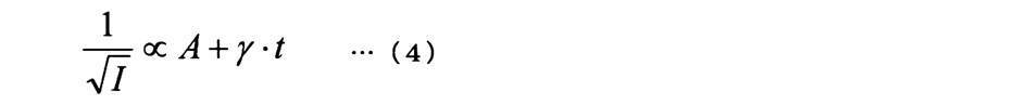
図6Aのグラフにて、時刻約3×10⁻⁸秒のところでパルス電圧を除去した。なお、図6Aのグラフは電圧を除去した時の輝度を1として表したものである。
電圧除去後、約2×10⁻⁷秒までの急速な減衰の後、緩やかな減衰成分が現れる。 The graph of FIG. 6A is a measurement example of a transient EL waveform when a predetermined pulse voltage is applied to the organic EL element and then the voltage is removed, and shows a change with time of the emission intensity of the organic EL element.
In the graph of FIG. 6A, the pulse voltage was removed at about 3 × 10 −8 seconds. Note that the graph of FIG. 6A represents the luminance when the voltage is removed as 1. FIG.
After voltage removal, a slow decay component appears after a rapid decay to about 2 × 10 −7 seconds.
直線部分を時間原点へ延長したときの縦軸との交点Aの値は1.55である。すると、この過渡EL波形から得られる遅延蛍光由来の発光強度比は、1/(1.55)2=0.41となる。つまり、41%が遅延蛍光由来であることになる。すなわち、TTF比率の理論限界と考えられる37.5%を超えるものである。
過渡EL波形から得られる遅延蛍光由来の発光強度は、測定する温度により変化している。このような現象は、主にTADF機構による蛍光発光特有のものと考えられる。
直線へのフィッティングは、最小二乗法により行うことが好ましい。この場合、10-5秒までの値を用いてフィッティングすることが好ましい。 The graph of FIG. 6B is a graph in which the reciprocal of the square root of the light intensity up to 1.5 × 10 −5 seconds after the voltage removal is plotted with the voltage removal time point as the origin. The fitting is performed as follows.
The value of the intersection A with the vertical axis when the straight line portion is extended to the time origin is 1.55. Then, the emission intensity ratio derived from delayed fluorescence obtained from this transient EL waveform is 1 / (1.55) 2 = 0.41. That is, 41% comes from delayed fluorescence. That is, it exceeds 37.5%, which is considered as the theoretical limit of the TTF ratio.
The emission intensity derived from delayed fluorescence obtained from the transient EL waveform varies depending on the temperature to be measured. Such a phenomenon is considered to be peculiar to fluorescence emission mainly by the TADF mechanism.
The fitting to a straight line is preferably performed by the least square method. In this case, the fitting is preferably performed using a value up to 10 −5 seconds.
上記したように、TTF機構は、2つの三重項励起子の衝突によって、一重項励起子が生成する現象を利用するものである。図7に示すように、ホスト材料の最低励起三重項状態T1Hは、ドーパント材料の最低励起三重項状態T1Dよりも小さいことが好ましいとされ、この結果、三重項励起子はホスト材料分子上に集中する。これらの三重項励起子の密度が高まることで三重項励起子同士が効率的に対衝突を起していき、一部は一重項励起子に変化することになる。TTF機構によって生成されたホスト材料の最低励起一重項状態S1Hは速やかにドーパント材料の最低励起一重項状態S1Dへのフェルスター移動を起こし、ドーパント材料が蛍光発光をする。 Here, a TTF mechanism having a light emission mechanism by delayed fluorescence will be described with reference to FIG. FIG. 7 shows the relationship between the energy levels of the host material and the dopant material in the organic EL element using the TTF mechanism. In FIG. 7, S0, S1 H, T1 H, S1 D, T1 D has the same meaning as in FIG. In FIG. 7, the arrows represent energy transfer between each excited state.
As described above, the TTF mechanism uses a phenomenon in which singlet excitons are generated by collision of two triplet excitons. As shown in FIG. 7, the lowest excited triplet state T1 H of the host material is preferably smaller than the lowest excited triplet state T1 D of the dopant material. As a result, the triplet exciton is present on the host material molecule. Concentrate on. As the density of these triplet excitons increases, the triplet excitons efficiently cause pair collisions, and part of them change to singlet excitons. The lowest excited singlet state S1 H of the host material generated by the TTF mechanism rapidly causes a Forster transfer to the lowest excited singlet state S1 D of the dopant material, and the dopant material emits fluorescence.
S.M.Bachiloらによれば(J.Phys.Cem.A,104,7711(2000))、五重項等の高次の励起子が、すぐに三重項に戻ると仮定すると、三重項励起子(以下、3A*と記載する)の密度が上がってきたとき、三重項励起子同士が衝突し下記数式(5)のような反応が起きる。ここで、1Aは基底状態、1A*は最低励起一重項励起子を表す。 The upper limit of the theoretical value of the TTF ratio can be obtained as follows.
According to SMBachilo et al. (J. Phys. Cem. A, 104, 7711 (2000)), assuming that higher-order excitons such as quintets immediately return to triplets, triplet excitons (hereinafter , 3 A * ) increases, and triplet excitons collide with each other to cause a reaction represented by the following formula (5). Here, 1 A represents the ground state, and 1 A * represents the lowest excited singlet exciton.
すなわち、
53A*→41A+1A*
となり、当初生成した75%の三重項励起子のうち、1/5、つまり20%が一重項励起子に変化することが予測されている。
従って、光として寄与する一重項励起子は、当初生成する25%分に75%×(1/5)=15%を加えた40%ということになる。
このとき、全発光強度中に占めるTTF由来の発光比率(TTF比率)は、15/40、すなわち37.5%となる。よって、本発明の有機EL素子の遅延蛍光比率は、TTF比率のみの理論値上限を上回ることが分かる。
That is,
5 3 A * → 4 1 A + 1 A *
Thus, it is predicted that 1/5, that is, 20% of the initially generated 75% triplet excitons will change to singlet excitons.
Therefore, the singlet excitons that contribute as light are 40%, which is 75% × (1/5) = 15% added to 25% initially generated.
At this time, the TTF-derived emission ratio (TTF ratio) in the total emission intensity is 15/40, that is, 37.5%. Therefore, it can be seen that the delayed fluorescence ratio of the organic EL device of the present invention exceeds the upper limit of the theoretical value of only the TTF ratio.
遅延蛍光の大きさを相対的に知る方法としては、1μsにおける残存強度を測定することが挙げられる。1μsにおける残存強度比は、過渡EL法により測定したパルス電圧を除去した時点における電圧に対する、パルス電圧を除去したのち1μs経過後の発光強度の比と定義する。過渡EL法により測定したパルス電圧を除去した後のEL発光の減衰挙動から、相対的な遅延蛍光の量を見積もることができる。1μsにおける残存強度比は、図6Aのグラフにおける1.0μs時の発光強度を読み取ることにより取得できる。
なお、1μsにおける残存強度比は、36.0%より大きいことが好ましい。さらに好ましくは、38.0%以上である。 -Residual intensity ratio at 1 μs As a method for relatively knowing the magnitude of delayed fluorescence, the residual intensity at 1 μs can be measured. The residual intensity ratio at 1 μs is defined as the ratio of the emission intensity after the elapse of 1 μs after removing the pulse voltage with respect to the voltage at the time when the pulse voltage measured by the transient EL method is removed. The amount of relative delayed fluorescence can be estimated from the decay behavior of the EL emission after removing the pulse voltage measured by the transient EL method. The residual intensity ratio at 1 μs can be obtained by reading the emission intensity at 1.0 μs in the graph of FIG. 6A.
The residual strength ratio at 1 μs is preferably larger than 36.0%. More preferably, it is 38.0% or more.
本発明における好ましいドーパント材料の特性としては、蛍光発光性で、かつ輻射遷移の速度定数が大きいものである。このような場合、ホスト材料で電気励起された一重項励起子及び、TADF機構によって生成された一重項励起子等は、ドーパント材料の一重項励起子にフェルスターエネルギー移動し、ドーパント材料は速やかに発光する。即ち、ホスト材料上の三重項励起子がTTAを起こす前に、上記エネルギー遷移を経て蛍光発光することが可能となり、高電流領域の効率低下が大きく改善される可能性がある。
本発明における輻射遷移の速度定数が大きいドーパント材料は、ドーパント材料の蛍光寿命が、5ns以下となるものを選択することが好ましい。さらに好ましくは、2ns以下であることである。また、ドーパント材料の蛍光量子収率は、溶液状態で80%以上であることが好ましい。蛍光量子収率は、例えば、浜松ホトニクス(株)製、絶対PL量子収率測定装置 C9920-02を用い、トルエン溶液中の濃度が10-5~10-6mol/lの範囲で測定することによって求めることができる。
また、輻射遷移の速度定数の大きいドーパント材料であることは、素子のELスペクトルを測定し、ドーパント材料の発光成分に対し、それ以外の発光成分が1/10以下であることを確認することからも推定される。 -Characteristics of dopants Preferred characteristics of the dopant material in the present invention include fluorescence and high rate constant of radiation transition. In such a case, singlet excitons electrically excited by the host material, singlet excitons generated by the TADF mechanism, etc. transfer Forster energy to the singlet excitons of the dopant material, and the dopant material rapidly Emits light. That is, before triplet excitons on the host material cause TTA, fluorescence can be emitted through the above energy transition, and the efficiency reduction in the high current region may be greatly improved.
As the dopant material having a large rate constant of radiation transition in the present invention, a dopant material having a fluorescence lifetime of 5 ns or less is preferably selected. More preferably, it is 2 ns or less. Moreover, it is preferable that the fluorescence quantum yield of dopant material is 80% or more in a solution state. The fluorescence quantum yield should be measured, for example, using an absolute PL quantum yield measuring device C9920-02 manufactured by Hamamatsu Photonics Co., Ltd. in a toluene solution with a concentration of 10 −5 to 10 −6 mol / l. Can be obtained.
Moreover, it is a dopant material with a large rate constant of a radiant transition from measuring the EL spectrum of an element, and confirming that other luminescent components are 1/10 or less with respect to the luminescent component of a dopant material. Is also estimated.
また、ホスト材料のΔST(H)が小さいと、ホスト材料と、発光層に隣接する電子輸送層とのエネルギー差が小さくなり、発光層に電子が注入しやすくなる。その結果、キャリアバランスが取りやすくなり、ロールオフが小さくなる -Relationship between the light-emitting layer and the electron transport layer Also, if ΔST (H) of the host material is small, the energy difference between the host material and the electron transport layer adjacent to the light-emitting layer is small, and electrons are injected into the light-emitting layer. It becomes easy. As a result, it becomes easier to balance the carrier and roll-off becomes smaller.
また、正孔輸送層のイオン化ポテンシャルをIPHTとしたとき、IPHT≦5.7eVであることが好ましい。これにより、電子と正孔とのバランスをより整えることが可能となる。イオン化ポテンシャルは、例えば、光電子分光装置(理研計器(株)製:AC-3)を用いて当該材料の薄膜状態で測定することによって求めることができる。 - the relationship between the light-emitting layer and the hole transporting layer also when the ionization potential of the hole transport layer and the IP HT, it is preferable that IP HT ≦ 5.7 eV. This makes it possible to further balance the electron and hole. The ionization potential can be obtained, for example, by measuring the material in a thin film state using a photoelectron spectrometer (manufactured by Riken Keiki Co., Ltd .: AC-3).
本発明において、ドーパント材料は、蛍光発光性のドーパント材料であり、ホスト材料に用いる化合物とドーパント材料に用いる化合物は、前記数式(2)のような一重項エネルギーの大小関係を満たす。
このような関係を満たすことで、ホスト材料の当初生成する一重項励起子と遅延蛍光由来の一重項励起子が、ドーパント材料へエネルギー移動し易くなる。その結果、ドーパント材料が効率良く蛍光発光する。 -Relationship between the singlet energy of the host material and the dopant material In the present invention, the dopant material is a fluorescent material dopant material, and the compound used for the host material and the compound used for the dopant material are as shown in the formula (2). Satisfies the magnitude relationship of singlet energy.
By satisfying such a relationship, the singlet excitons initially generated in the host material and the singlet excitons derived from delayed fluorescence can be easily transferred to the dopant material. As a result, the dopant material efficiently emits fluorescence.
本発明者らは、ΔSTを小さくする手段の一つとして会合体を形成する化合物を用いることを見出し、Δnが大きい化合物は、当該化合物の膜内において会合体を形成し易いことを見出した。ここでのΔnとは、分光エリプソメトリー測定(測定範囲:200nm~1000nm)において屈折率と同時に観測される反射率が観測されない領域において、シリコン基板面に対して垂直方向の屈折率nZと、シリコン基板に対して平行方向の屈折率nXとの差が最も大きい時の値を取ったものである。
Δnの大きさと会合体の形成し易さとの関連性は、次のように推測される。
シリコン基板面に対して垂直方向zと平行方向xの屈折率nに大きな違いが生じる場合は、薄膜状態において分子が、ある程度の規則性を有する状態で存在していることを意味していると考えられる。すなわち、本発明のホスト材料に用いる化合物は、所定の大きさのΔnを有する化合物であり、薄膜状態において会合体を形成し、ある程度の規則性を有して存在していると推測される。
一方で、このΔnが非常に小さい化合物、例えば、CBPやAlq3などは、薄膜状態において分子が全く規則性を有していないアモルファス状態で存在している。
Δnの大きさと会合体の形成し易さとの関連性については、例えば、
文献6:D. Yokoyama et al., Org. Electron. 10, 127-137 (2009)、
文献7:D. Yokoyama et al., Appl. Phys. Lett. 93, 173302 (2008)、
文献8:D. Yokoyama et al., Appl. Phys. Lett. 95, 243303 (2009)、
の文献に記載されている。 ・ Δn
The present inventors have found that a compound that forms an aggregate is used as one means for reducing ΔST, and that a compound having a large Δn easily forms an aggregate in the film of the compound. Here, Δn is a refractive index n Z in a direction perpendicular to the silicon substrate surface in a region where a reflectance observed simultaneously with a refractive index in spectroscopic ellipsometry measurement (measurement range: 200 nm to 1000 nm) is not observed. The value when the difference from the refractive index n X in the direction parallel to the silicon substrate is the largest is taken.
The relationship between the magnitude of Δn and the ease of forming aggregates is presumed as follows.
When there is a large difference in the refractive index n between the vertical direction z and the parallel direction x with respect to the silicon substrate surface, it means that molecules exist in a state having a certain degree of regularity in the thin film state. Conceivable. That is, the compound used for the host material of the present invention is a compound having a predetermined Δn, forms an aggregate in a thin film state, and is presumed to exist with a certain degree of regularity.
On the other hand, a compound having a very small Δn, such as CBP or Alq 3 , exists in an amorphous state where the molecules have no regularity in the thin film state.
Regarding the relationship between the size of Δn and the ease of forming aggregates, for example,
Reference 6: D. Yokoyama et al., Org. Electron. 10, 127-137 (2009),
Reference 7: D. Yokoyama et al., Appl. Phys. Lett. 93, 173302 (2008),
Reference 8: D. Yokoyama et al., Appl. Phys. Lett. 95, 243303 (2009),
In the literature.
各化合物をシリコン基板(Si(100))上に蒸着し、厚さ100nmの有機薄膜を形成する。そして多入角高速分光エリプソメータ(J.A.Woollam社製、M-2000D)を用い、入射角45度から80度(5度おき)、波長200nmから1000nm(1.6nmおき)の範囲でエリプソパラメーターψおよびΔを測定する。得られたパラメーターに対し、解析ソフトWVASE32(J.A.Woollam社製)を用いて一括解析を行う事で、膜の光学異方性を調べる。膜の光学定数(屈折率nや消衰係数k)の異方性が、膜内における分子配向の異方性を反映する。詳細な測定方法・解析方法は、上記文献6~8に記載されている。
Δnは、シリコン基板面に対して垂直方向zと平行方向xの屈折率nの差として求めることができる。シリコン基板面に対する垂直方向z、及び平行方向xについては、図8Aに示す。 Δn can be calculated based on the refractive index of each compound measured by spectroscopic ellipsometry. Spectral ellipsometry is a method for measuring the optical constant (refractive index n and extinction coefficient k) and film thickness of a thin film. For example, a multi-angle high-speed spectroscopic ellipsometer (manufactured by JA Woollam, M-2000D). Can be used. 8A and 8B show an example of spectroscopic ellipsometry measurement. FIG. 8A shows an incident angle of incident light from a light source, and FIG. 8B shows a cross-sectional view of an organic thin film on a silicon substrate to be measured.
Each compound is deposited on a silicon substrate (Si (100)) to form an organic thin film having a thickness of 100 nm. Then, using a multi-incidence high-speed spectroscopic ellipsometer (JA Woollam, M-2000D), an ellipso with an incident angle of 45 ° to 80 ° (every 5 °) and a wavelength of 200 nm to 1000 nm (every 1.6 nm). The parameters ψ and Δ are measured. The optical anisotropy of the film is examined by performing batch analysis on the obtained parameters using analysis software WVASE32 (manufactured by JA Woollam). The anisotropy of the optical constant (refractive index n and extinction coefficient k) of the film reflects the anisotropy of molecular orientation in the film. Detailed measurement methods and analysis methods are described in the
Δn can be obtained as a difference in refractive index n between the vertical direction z and the parallel direction x with respect to the silicon substrate surface. The vertical direction z and the parallel direction x with respect to the silicon substrate surface are shown in FIG. 8A.
半値幅は、発光スペクトルの最大発光強度に対して発光強度が半分になった時の発光スペクトルの幅を示す。本発明者は、ホスト材料のフォトルミネッセンススペクトルの半値幅が50nm以上であることによって、ホスト材料が会合状態を形成しやすい材料であって、薄膜中での逆項間交差の起こしやすい材料であることを見出した。したがって、フォトルミネッセンススペクトルの半値幅が50nm以上であるホスト材料では、TADF機構が起こりやすい。特に好ましくは、ホスト材料のフォトルミネッセンススペクトルの半値幅が75nm以上である。 -Half width The half width indicates the width of the emission spectrum when the emission intensity is halved with respect to the maximum emission intensity of the emission spectrum. The inventor of the present invention is a material in which the host material easily forms an association state when the half width of the photoluminescence spectrum of the host material is 50 nm or more, and is a material in which reverse intersystem crossing easily occurs in a thin film. I found out. Therefore, the TADF mechanism is likely to occur in the host material having a half width of the photoluminescence spectrum of 50 nm or more. Particularly preferably, the half width of the photoluminescence spectrum of the host material is 75 nm or more.
本発明において、ホスト材料の三重項エネルギーEg77K(H)と、ドーパント材料の三重項エネルギーEg77K(D)との差ΔTが、上記数式(3)の関係を満たすことが好ましい。また、ΔTが、0.8eV以上であることがより好ましく、1.0eV以上であることがよりさらに好ましい。
ΔTが数式(3)の関係を満たすことで、再結合により生成したホスト材料上の三重項励起子が、ドーパント材料の三重項準位にエネルギー移動し難くなり、三重項励起子が熱失活し難くなると考えられるからである。その結果、ドーパント材料が効率良く蛍光発光する。 ・ ΔT
In the present invention, it is preferable that the difference ΔT between the triplet energy Eg 77K (H) of the host material and the triplet energy Eg 77K (D) of the dopant material satisfies the relationship of the above formula (3). Further, ΔT is more preferably 0.8 eV or more, and further preferably 1.0 eV or more.
When ΔT satisfies the relationship of Equation (3), triplet excitons on the host material generated by recombination become difficult to transfer energy to the triplet level of the dopant material, and the triplet excitons are thermally deactivated. It is because it is thought that it becomes difficult to do. As a result, the dopant material efficiently emits fluorescence.
上記数式(1)、及び(2)の関係を満たす、ホスト材料、及びドーパント材料に用いる化合物は、次の通りである。 (Compound of light emitting layer)
The compounds used for the host material and the dopant material satisfying the relations of the above formulas (1) and (2) are as follows.
ホスト材料としては、カルバゾール誘導体、ビスカルバゾール誘導体、インドロカルバゾール誘導体、アクリジン誘導体、オキサジン誘導体、ピラジン誘導体、ピリミジン誘導体、トリアジン誘導体、ジベンゾフラン誘導体、ジベンゾチオフェン誘導体などが挙げられる。これらの誘導体は、適宜、置換基を保有してもよい。
置換基としては、炭素数6~40のアリール基、炭素数2~40の複素環基、トリアルキルシリル基、ジアルキルアリールシリル基、アルキルジアリールシリル基、トリアリールシリル基、フッ素原子、シアノ基等があげられる。この置換基におけるトリアルキルシリル基、ジアルキルアリールシリル基、アルキルジアリールシリル基、及びトリアリールシリル基は、炭素数1~30のアルキル基、及び炭素数6~30のアリール基の少なくともいずれかを含む。なお、水素原子には重水素原子を含む。
また、ホスト材料として好ましくは、カルバゾール構造、ビスカルバゾール構造、インドロカルバゾール構造、アクリジン構造から選ばれる少なくとも1種と、オキサジン構造、ピラジン構造、ピリミジン構造、トリアジン構造、ジベンゾフラン構造から選ばれる少なくとも1種とが結合した構造の化合物が挙げられる。
これらの構造が結合するとは各種、連結基で結合することを意味する。好ましい連結基は、単結合、フェニレン構造、メタビフェニレン構造である。
カルバゾール構造、インドロカルバゾール構造、アクリジン構造、オキサジン構造、ピラジン構造、ピリミジン構造、トリアジン構造、ジベンゾフラン構造とは、それぞれ、インドロカルバゾール、アクリジン、オキサジン、ピラジン、ピリミジン、トリアジン、ジベンゾフランを部分構造とするものも含む環構造をいう。
また、カルバゾール構造、ビスカルバゾール構造、インドロカルバゾール構造、アクリジン構造、オキサジン構造、ピラジン構造、ピリミジン構造、トリアジン構造、ジベンゾフラン構造は適宜、置換基を保有してもよい。
置換基としては、炭素数6~40のアリール基、炭素数2~40の複素環基、トリアルキルシリル基、ジアルキルアリールシリル基、アルキルジアリールシリル基、トリアリールシリル基、フッ素原子、シアノ基等があげられる。この置換基におけるトリアルキルシリル基、ジアルキルアリールシリル基、アルキルジアリールシリル基、及びトリアリールシリル基は、炭素数1~30のアルキル基、及び炭素数6~30のアリール基の少なくともいずれかを含む。なお、水素原子には重水素原子を含む。 Host material Examples of the host material include carbazole derivatives, biscarbazole derivatives, indolocarbazole derivatives, acridine derivatives, oxazine derivatives, pyrazine derivatives, pyrimidine derivatives, triazine derivatives, dibenzofuran derivatives, dibenzothiophene derivatives, and the like. These derivatives may appropriately have a substituent.
Examples of the substituent include aryl groups having 6 to 40 carbon atoms, heterocyclic groups having 2 to 40 carbon atoms, trialkylsilyl groups, dialkylarylsilyl groups, alkyldiarylsilyl groups, triarylsilyl groups, fluorine atoms, cyano groups, and the like. Is given. The trialkylsilyl group, dialkylarylsilyl group, alkyldiarylsilyl group, and triarylsilyl group in this substituent include at least one of an alkyl group having 1 to 30 carbon atoms and an aryl group having 6 to 30 carbon atoms. . Note that a hydrogen atom includes a deuterium atom.
The host material is preferably at least one selected from a carbazole structure, a biscarbazole structure, an indolocarbazole structure, and an acridine structure, and at least one selected from an oxazine structure, a pyrazine structure, a pyrimidine structure, a triazine structure, and a dibenzofuran structure. And a compound having a structure in which and are bonded.
The bonding of these structures means bonding with various linking groups. Preferred linking groups are a single bond, a phenylene structure, and a metabiphenylene structure.
The carbazole structure, indolocarbazole structure, acridine structure, oxazine structure, pyrazine structure, pyrimidine structure, triazine structure, and dibenzofuran structure are partial structures of indolocarbazole, acridine, oxazine, pyrazine, pyrimidine, triazine, and dibenzofuran, respectively. It also refers to a ring structure that includes things.
The carbazole structure, biscarbazole structure, indolocarbazole structure, acridine structure, oxazine structure, pyrazine structure, pyrimidine structure, triazine structure, and dibenzofuran structure may have a substituent as appropriate.
Examples of the substituent include aryl groups having 6 to 40 carbon atoms, heterocyclic groups having 2 to 40 carbon atoms, trialkylsilyl groups, dialkylarylsilyl groups, alkyldiarylsilyl groups, triarylsilyl groups, fluorine atoms, cyano groups, and the like. Is given. The trialkylsilyl group, dialkylarylsilyl group, alkyldiarylsilyl group, and triarylsilyl group in this substituent include at least one of an alkyl group having 1 to 30 carbon atoms and an aryl group having 6 to 30 carbon atoms. . Note that a hydrogen atom includes a deuterium atom.
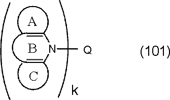
環A,環B,環Cは、
炭素原子、窒素原子、酸素原子、硫黄原子、ケイ素原子から選ばれる原子を環構成原子として有する置換または無置換の5~7員環であり、
環Aと環B,および環Cと環Bは縮合している。
環Cには、さらに別の環が縮合されていてもよい。
Qは、下記一般式(103)で表される基である。
kは1または2である。) (In general formula (101),
Ring A, Ring B, and Ring C are
A substituted or unsubstituted 5- to 7-membered ring having an atom selected from a carbon atom, a nitrogen atom, an oxygen atom, a sulfur atom, and a silicon atom as a ring constituent atom;
Ring A and ring B, and ring C and ring B are fused.
Ring C may be further condensed with another ring.
Q is a group represented by the following general formula (103).
k is 1 or 2. )
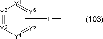
Y1~Y6の少なくとも1個はLに結合する炭素原子であり、
Y1~Y6のうち1~3個は窒素原子であり、
Y1~Y6のうちLに結合する炭素原子または窒素原子以外のものは、CAr1である。
Ar1は置換または無置換の芳香族炭化水素基である。
一般式(103)が複数のCAr1を有する場合、Ar1は互いに同一または異なる。
Lは単結合または連結基を表す。) (In general formula (103),
At least one of Y 1 to Y 6 is a carbon atom bonded to L;
1 to 3 of Y 1 to Y 6 are nitrogen atoms,
Of Y 1 to Y 6 , other than the carbon atom or nitrogen atom bonded to L is CAr 1 .
Ar 1 is a substituted or unsubstituted aromatic hydrocarbon group.
When General Formula (103) has a plurality of CAr 1 , Ar 1 are the same or different from each other.
L represents a single bond or a linking group. )
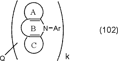
Arは置換または無置換の芳香族炭化水素基である。) (In General Formula (102), Ring A, Ring B, Ring C, Q, and k are as defined in General Formula (101) above.
Ar is a substituted or unsubstituted aromatic hydrocarbon group. )
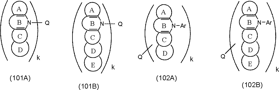
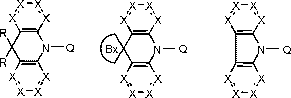
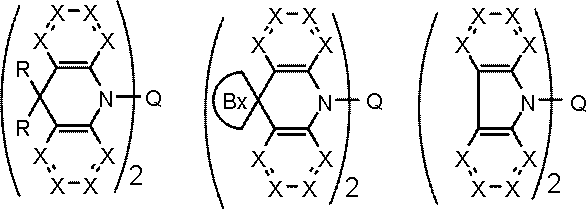
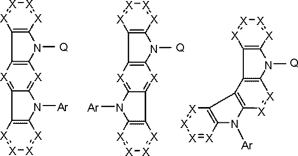
Rxは置換基を表す。
Bxは炭素原子で形成される5~7員環である。) (In the above general formula, R is an alkyl group, X is CH, CRx, or a nitrogen atom.
Rx represents a substituent.
Bx is a 5- to 7-membered ring formed of carbon atoms. )
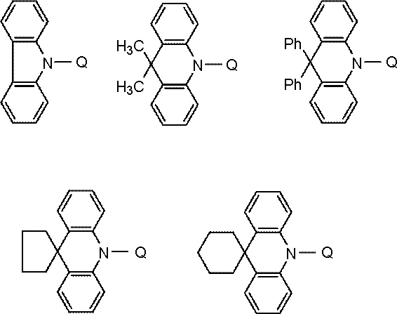
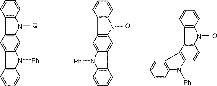

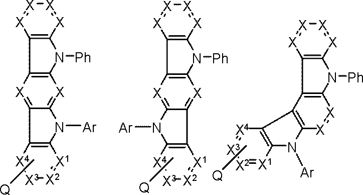
X,X1~X4はCH、CRxまたは窒素原子である。
Rxは、置換基を表す。
ただし、X1~X4のうち1つは、Qに結合する炭素原子である。
Bxは炭素原子で形成される5~7員環である。
Arは芳香族炭化水素基、Phはフェニル基を表す。) (In the above general formula, R is an alkyl group.
X and X 1 to X 4 are CH, CRx, or a nitrogen atom.
Rx represents a substituent.
However, one of X 1 to X 4 is a carbon atom bonded to Q.
Bx is a 5- to 7-membered ring formed of carbon atoms.
Ar represents an aromatic hydrocarbon group, and Ph represents a phenyl group. )
上記一般式(102)で表される化合物は、さらに好ましくは、下記一般式で表される化合物である。 Of the compounds represented by the above general formula, those in which X 1 or X 3 is a carbon atom bonded to Q are preferred.
The compound represented by the general formula (102) is more preferably a compound represented by the following general formula.
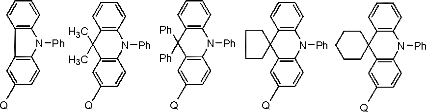
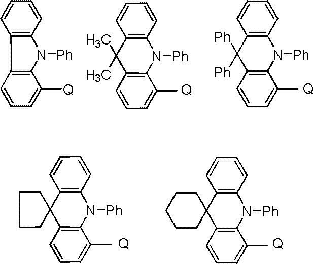
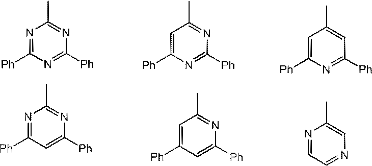
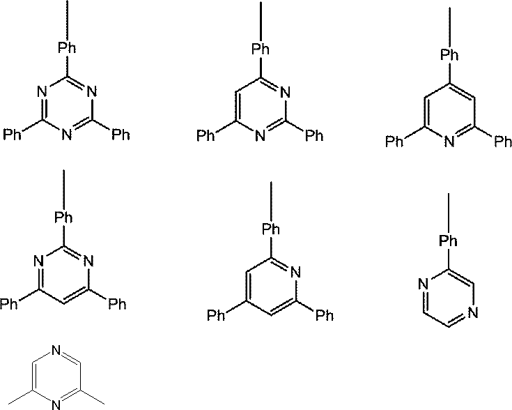
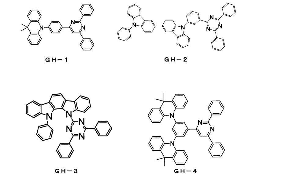
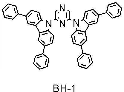
本発明では、上記のとおり、発光層のドーパント材料に蛍光発光性のドーパント材料を用いる。
蛍光発光性ドーパント材料としては、公知の蛍光発光性材料を用いることができる。具体的には、例えば、ビスアリールアミノナフタレン誘導体、アリール置換ナフタレン誘導体、ビスアリールアミノアントラセン誘導体、アリール基置換アントラセン誘導体、ビスアリールアミノピレン誘導体、アリール基置換ピレン誘導体、ビスアリールアミノクリセン誘導体、アリール置換クリセン誘導体、ビスアリールアミノフルオランテン誘導体、アリール置換フルオランテン誘導体、インデノペリレン誘導体、ピロメテンホウ素錯体化合物、ピロメテン骨格を有する化合物もしくはその金属錯体、ジケトピロロピロール誘導体、ペリレン誘導体が挙げられる。 -Dopant material In this invention, as above-mentioned, a fluorescent material is used for the dopant material of a light emitting layer.
A known fluorescent material can be used as the fluorescent material. Specifically, for example, bisarylaminonaphthalene derivatives, aryl-substituted naphthalene derivatives, bisarylaminoanthracene derivatives, aryl group-substituted anthracene derivatives, bisarylaminopyrene derivatives, aryl group-substituted pyrene derivatives, bisarylaminochrysene derivatives, aryl-substituted Examples include chrysene derivatives, bisarylaminofluoranthene derivatives, aryl-substituted fluoranthene derivatives, indenoperylene derivatives, pyromethene boron complex compounds, compounds having a pyromethene skeleton or metal complexes thereof, diketopyrrolopyrrole derivatives, and perylene derivatives.
本発明の有機EL素子は、透光性の基板上に作製する。この透光性基板は、有機EL素子を構成する陽極、有機化合物層、陰極等を支持する基板であり、400nm以上700nm以下の可視領域の光の透過率が50%以上で平滑な基板が好ましい。
透光性基板としては、ガラス板やポリマー板などが挙げられる。
ガラス板としては、特にソーダ石灰ガラス、バリウム・ストロンチウム含有ガラス、鉛ガラス、アルミノケイ酸ガラス、ホウケイ酸ガラス、バリウムホウケイ酸ガラス、石英などを原料として用いてなるものを挙げられる。
またポリマー板としては、ポリカーボネート、アクリル、ポリエチレンテレフタレート、ポリエーテルサルファイド、ポリサルフォンなどを原料として用いてなるものを挙げることができる。 (substrate)
The organic EL element of the present invention is produced on a translucent substrate. This translucent substrate is a substrate that supports an anode, an organic compound layer, a cathode, and the like constituting the organic EL element, and is preferably a smooth substrate having a light transmittance in the visible region of 400 nm to 700 nm of 50% or more. .
Examples of the translucent substrate include a glass plate and a polymer plate.
Examples of the glass plate include those using soda lime glass, barium / strontium-containing glass, lead glass, aluminosilicate glass, borosilicate glass, barium borosilicate glass, quartz and the like as raw materials.
Examples of the polymer plate include those using polycarbonate, acrylic, polyethylene terephthalate, polyether sulfide, polysulfone and the like as raw materials.
有機EL素子の陽極は、正孔を発光層に注入する役割を担うものであり、4.5eV以上の仕事関数を有することが効果的である。
陽極材料の具体例としては、酸化インジウム錫合金(ITO)、酸化錫(NESA)、酸化インジウム亜鉛酸化物、金、銀、白金、銅などが挙げられる。
発光層からの発光を陽極側から取り出す場合、陽極の可視領域の光の透過率を10%より大きくすることが好ましい。また、陽極のシート抵抗は、数百Ω/□(Ω/sq。オーム・パー・スクウェア。)以下が好ましい。陽極の膜厚は、材料にもよるが、通常10nm以上1μm以下、好ましくは10nm以上200nm以下の範囲で選択される。 (Anode and cathode)
The anode of the organic EL element plays a role of injecting holes into the light emitting layer, and it is effective to have a work function of 4.5 eV or more.
Specific examples of the anode material include indium tin oxide alloy (ITO), tin oxide (NESA), indium zinc oxide, gold, silver, platinum, and copper.
When light emitted from the light-emitting layer is extracted from the anode side, it is preferable that the light transmittance in the visible region of the anode be greater than 10%. The sheet resistance of the anode is preferably several hundred Ω / □ (Ω / sq. Ohm per square) or less. Although the film thickness of the anode depends on the material, it is usually selected in the range of 10 nm to 1 μm, preferably 10 nm to 200 nm.
陰極材料は特に限定されないが、具体的にはインジウム、アルミニウム、マグネシウム、マグネシウム-インジウム合金、マグネシウム-アルミニウム合金、アルミニウム-リチウム合金、アルミニウム-スカンジウム-リチウム合金、マグネシウム-銀合金などが使用できる。
陰極も、陽極と同様に、蒸着法などの方法で、例えば、電子輸送層や電子注入層上に薄膜を形成できる。また、陰極側から、発光層からの発光を取り出す態様を採用することもできる。発光層からの発光を陰極側から取り出す場合、陰極の可視領域の光の透過率を10%より大きくすることが好ましい。
陰極のシート抵抗は、数百Ω/□以下が好ましい。
陰極の膜厚は、材料にもよるが、通常10nm以上1μm以下、好ましくは50nm以上200nm以下の範囲で選択される。 As the cathode, a material having a small work function is preferable for the purpose of injecting electrons into the light emitting layer.
The cathode material is not particularly limited, and specifically, indium, aluminum, magnesium, magnesium-indium alloy, magnesium-aluminum alloy, aluminum-lithium alloy, aluminum-scandium-lithium alloy, magnesium-silver alloy and the like can be used.
Similarly to the anode, the cathode can be formed, for example, on the electron transport layer or the electron injection layer by a method such as vapor deposition. Moreover, the aspect which takes out light emission from a light emitting layer from a cathode side is also employable. When light emitted from the light emitting layer is extracted from the cathode side, it is preferable that the light transmittance in the visible region of the cathode be greater than 10%.
The sheet resistance of the cathode is preferably several hundred Ω / □ or less.
The thickness of the cathode depends on the material, but is usually selected in the range of 10 nm to 1 μm, preferably 50 nm to 200 nm.
正孔注入・輸送層は、発光層への正孔注入を助け、発光領域まで輸送する層であって、正孔移動度が大きく、イオン化エネルギーが小さい化合物が用いられる。
正孔注入・輸送層を形成する材料としては、より低い電界強度で正孔を発光層に輸送する材料が好ましく、例えば、芳香族アミン化合物が好適に用いられる。 (Hole injection / transport layer)
The hole injection / transport layer is a layer that assists hole injection into the light emitting layer and transports it to the light emitting region, and a compound having a high hole mobility and a low ionization energy is used.
As a material for forming the hole injecting / transporting layer, a material that transports holes to the light emitting layer with lower electric field strength is preferable. For example, an aromatic amine compound is preferably used.
電子注入・輸送層は、発光層への電子の注入を助け、発光領域まで輸送する層であって、電子移動度が大きい化合物が用いられる。
電子注入・輸送層に用いられる化合物としては、例えば、分子内にヘテロ原子を1個以上含有する芳香族ヘテロ環化合物が好ましく用いられ、特に含窒素環誘導体が好ましい。含窒素環誘導体としては、含窒素6員環もしくは5員環骨格を有する複素環化合物が好ましい。 (Electron injection / transport layer)
The electron injection / transport layer is a layer that assists injection of electrons into the light emitting layer and transports it to the light emitting region, and a compound having a high electron mobility is used.
As the compound used in the electron injecting / transporting layer, for example, an aromatic heterocyclic compound containing one or more hetero atoms in the molecule is preferably used, and a nitrogen-containing ring derivative is particularly preferable. As the nitrogen-containing ring derivative, a heterocyclic compound having a nitrogen-containing 6-membered ring or 5-membered ring skeleton is preferable.
本発明の有機EL素子の各層の形成方法としては、上記で特に言及した以外には制限されないが、真空蒸着、スパッタリング、プラズマ、イオンプレーティングなどの乾式成膜法や、スピンコーティング、ディッピング、フローコーティング、インクジェットなどの湿式成膜法などの公知の方法を採用することができる。 (Layer formation method)
The method for forming each layer of the organic EL element of the present invention is not limited except as specifically mentioned above, but is a dry film forming method such as vacuum deposition, sputtering, plasma, ion plating, spin coating, dipping, flow. A known method such as a wet film forming method such as coating or ink jetting can be employed.
本発明の有機EL素子の各有機層の膜厚は、上記で特に言及した以外には制限されないが、一般に膜厚が薄すぎるとピンホール等の欠陥が生じやすく、逆に厚すぎると高い印加電圧が必要となり効率が悪くなるため、通常は数nmから1μmの範囲が好ましい。 (Film thickness)
The film thickness of each organic layer of the organic EL device of the present invention is not limited except as specifically mentioned above, but in general, if the film thickness is too thin, defects such as pinholes are likely to occur. Since a voltage is required and efficiency is lowered, the range of several nm to 1 μm is usually preferable.
なお、本発明は、上述の実施形態に限定されるものではなく、本発明の目的を達成できる範囲での変更、改良などは、本発明に含まれるものである。 [Modification of Embodiment]
In addition, this invention is not limited to the above-mentioned embodiment, The change in the range which can achieve the objective of this invention, improvement, etc. are included in this invention.
また、有機EL素子が複数の発光層を有する場合、これらの発光層が互いに隣接して設けられていてもよい。 The light emitting layer is not limited to one layer, and a plurality of light emitting layers may be stacked. When the organic EL element has a plurality of light emitting layers, it is sufficient that at least one light emitting layer contains the host material and the fluorescent dopant material defined in the present invention, and the other light emitting layers emit fluorescent light. It may be a layer or a phosphorescent light emitting layer.
Moreover, when an organic EL element has a several light emitting layer, these light emitting layers may be provided adjacent to each other.

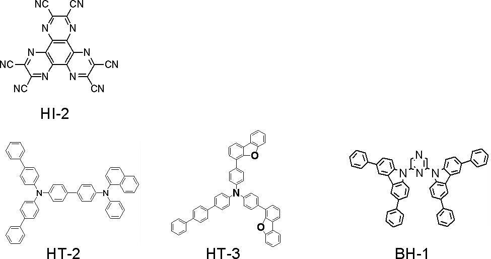
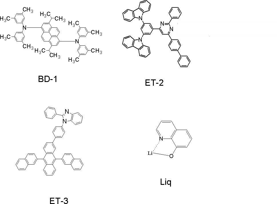
〔合成例1〕 GH-4の合成
アルゴン雰囲気下、特開2010-180204号公報に記載の方法に従って合成した中間体A(4.4g、21mmol)、国際公開第2003/080760号に記載の方法に従って合成した中間体B(4.7g、10mmol)、トリス(ジベンジリデンアセトン)ジパラジウム(0.37g、0.4mmol)、トリ-t-ブチルホスホニウムテトラフルオロほう酸塩(0.46g、1.6mmol)、t-ブトキシナトリウム(2.7g、28mmol)、無水トルエン(100mL)を順次加えて8時間加熱還流した。
室温まで反応液を冷却した後、有機層を分離し、有機溶媒を減圧下で留去した。得られた残渣をシリカゲルカラムクロマトグラフィーにて精製し、目的化合物GH-4(3.6g、収率50%)を得た。
FD-MS分析の結果、分子量722に対してm/e=722であった。
以下に目的化合物GH-4の合成スキームを示す。 <Synthesis of compounds>
[Synthesis Example 1] Synthesis of GH-4 Intermediate A (4.4 g, 21 mmol) synthesized according to the method described in JP2010-180204A in an argon atmosphere, the method described in WO2003 / 080760 Intermediate B (4.7 g, 10 mmol), tris (dibenzylideneacetone) dipalladium (0.37 g, 0.4 mmol), tri-t-butylphosphonium tetrafluoroborate (0.46 g, 1.6 mmol) synthesized according to ), Sodium t-butoxy (2.7 g, 28 mmol) and anhydrous toluene (100 mL) were sequentially added, and the mixture was heated to reflux for 8 hours.
After cooling the reaction solution to room temperature, the organic layer was separated, and the organic solvent was distilled off under reduced pressure. The obtained residue was purified by silica gel column chromatography to obtain the target compound GH-4 (3.6 g, yield 50%).
As a result of FD-MS analysis, it was m / e = 722 with respect to the molecular weight 722.
The synthesis scheme of the target compound GH-4 is shown below.
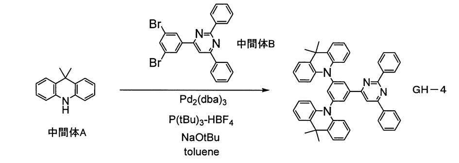

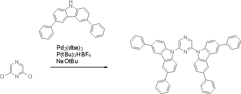
室温まで反応液を冷却した後、有機層を分離し、有機溶媒を減圧下留去した。得られた残渣をシリカゲルカラムクロマトグラフィーにて精製し、1.8gの固体を得た。
得られた化合物について、FD-MSを行った結果、化合物BH-1と同定した。
FD-MS:
calcd for C52H34N4=714,found m/z=714(M+,100) Under an argon atmosphere, 2,6-dichloropyrazine (0.6 g, 3.9 mmol), 3,6-dibromocarbazole (2.6 g, 8 mmol), tris (dibenzylideneacetone) dipalladium (0.07 g, 0.08 mmol) ), Tri-t-butylphosphonium tetrafluoroborate (0.09 g, 0.3 mmol), t-butoxy sodium (0.5 g, 5.5 mmol), and anhydrous toluene (20 mL) were sequentially added and heated for 8 hours. Refluxed.
After cooling the reaction solution to room temperature, the organic layer was separated, and the organic solvent was distilled off under reduced pressure. The obtained residue was purified by silica gel column chromatography to obtain 1.8 g of a solid.
The obtained compound was subjected to FD-MS and identified as Compound BH-1.
FD-MS:
calcd for C 52 H 34 N 4 = 714, found m / z = 714 (M +, 100)
次に、本実施例で使用した化合物の物性を測定した。対象化合物は、GH-4、GD-1、BH-1、BD-1である。測定方法、又は算出方法を以下に示すとともに、測定結果、又は算出結果を表1に示す。
(1)一重項エネルギーEgS
一重項エネルギーEgSは、以下の方法により求めた。
測定対象化合物を石英基板上に蒸着して試料を作製し、常温(300K)でこの試料の吸収スペクトルを測定した。試料の膜厚は100nmとした。吸収スペクトルは、縦軸を吸光度、横軸を波長とした。この吸収スペクトルの長波長側の立ち下がりに対して接線を引き、その接線と横軸との交点の波長値λedge[nm]を求めた。この波長値を次に示す換算式でエネルギー値に換算した値をEgSとした。
換算式:EgS[eV]=1239.85/λedge
吸収スペクトルの測定には、分光光度計(日立製、U3310)を用いた。 <Evaluation of compound>
Next, the physical properties of the compounds used in this example were measured. The target compounds are GH-4, GD-1, BH-1, and BD-1. The measurement method or calculation method is shown below, and the measurement result or calculation result is shown in Table 1.
(1) Singlet energy EgS
Singlet energy EgS was determined by the following method.
The sample to be measured was deposited on a quartz substrate to prepare a sample, and the absorption spectrum of this sample was measured at room temperature (300K). The film thickness of the sample was 100 nm. In the absorption spectrum, the vertical axis represents absorbance and the horizontal axis represents wavelength. A tangent line was drawn with respect to the fall of the absorption spectrum on the long wavelength side, and a wavelength value λ edge [nm] at the intersection of the tangent line and the horizontal axis was obtained. A value obtained by converting this wavelength value into an energy value by the following conversion formula was defined as EgS.
Conversion formula: EgS [eV] = 1239.85 / λedge
A spectrophotometer (Hitachi, U3310) was used for the measurement of the absorption spectrum.
なお、吸光度の値が0.2以下の極大点は、上記最も長波長側の極大値には含めなかった。 In addition, the tangent with respect to the fall of the long wavelength side of an absorption spectrum was drawn as follows. When moving on the spectrum curve in the long wavelength direction from the maximum value on the longest wavelength side among the maximum values of the absorption spectrum, the tangent at each point on the curve is considered. This tangent repeats as the curve falls (ie, as the value on the vertical axis decreases), the slope decreases and then increases. The tangent drawn at the point where the slope value takes the minimum value on the long wavelength side (except when the absorbance is 0.1 or less) is taken as the tangent to the fall on the long wavelength side of the absorption spectrum.
In addition, the maximum point whose absorbance value is 0.2 or less was not included in the maximum value on the longest wavelength side.
Eg77K、及びEgTDは、以下の方法により求めた。
各化合物を、公知の燐光測定法(例えば、「光化学の世界」(日本化学会編・1993)50頁付近の記載の方法)により測定した。具体的には、各化合物を溶媒に溶解(試料10[μmol/リットル]、EPA(ジエチルエーテル:イソペンタン:エタノール=5:5:5(容積比)、各溶媒は分光用グレード)し、燐光測定用試料とした。石英セルへ入れた燐光測定用試料を77[K]に冷却し、励起光を燐光測定用試料に照射し、波長を変えながら燐光強度を測定した。燐光スペクトルは、縦軸を燐光強度、横軸を波長とした。
この燐光スペクトルの短波長側の立ち上がりに対して接線を引き、その接線と横軸との交点の波長値λedge[nm]を求めた。この波長値を次に示す換算式でエネルギー値に換算した値をEg77K(H)又はEgTD(Eg77K(D))とした。
換算式:Eg77K(H)[eV]=1239.85/λedge
:EgTD[eV]=1239.85/λedge (2) Energy gap Eg 77K, and triplet energy EgT D
Eg 77K, and EgT D was determined by the following method.
Each compound was measured by a known phosphorescence measurement method (for example, “the world of photochemistry” (edited by the Chemical Society of Japan, 1993), page 50). Specifically, each compound is dissolved in a solvent (sample 10 [μmol / liter], EPA (diethyl ether: isopentane: ethanol = 5: 5: 5 (volume ratio), each solvent is a spectroscopic grade), and phosphorescence measurement is performed. The phosphorescence measurement sample placed in the quartz cell was cooled to 77 [K], the excitation light was irradiated onto the phosphorescence measurement sample, and the phosphorescence intensity was measured while changing the wavelength. Is the phosphorescence intensity, and the horizontal axis is the wavelength.
A tangent line was drawn with respect to the rising edge of the phosphorescence spectrum on the short wavelength side, and a wavelength value λ edge [nm] at the intersection of the tangent line and the horizontal axis was obtained. A value obtained by converting the wavelength value into an energy value by the following conversion formula was defined as Eg 77K (H) or EgT D (Eg 77K (D)).
Conversion formula: Eg 77K (H) [eV] = 1239.85 / λedge
: EgT D [eV] = 1239.85 / λedge
なお、スペクトルの最大ピーク強度の10%以下のピーク強度をもつ極大点は、上述の最も短波長側の極大値には含めず、最も短波長側の極大値に最も近い、傾きの値が極大値をとる点において引いた接線を当該燐光スペクトルの短波長側の立ち上がりに対する接線とする。
燐光の測定には、(株)日立ハイテクノロジー製のF-4500形分光蛍光光度計本体と低温測定用オプション備品を用いた。なお、測定装置はこの限りではなく、冷却装置及び低温用容器と、励起光源と、受光装置とを組み合わせることにより、測定してもよい。 The tangent to the short wavelength rising edge of the phosphorescence spectrum was drawn as follows. When moving on the spectrum curve from the short wavelength side of the phosphorescence spectrum to the maximum value on the shortest wavelength side among the maximum values of the spectrum, tangents at each point on the curve are considered toward the long wavelength side. The slope of this tangent line increases as the curve rises (that is, as the vertical axis increases). The tangent drawn at the point where the value of the slope takes the maximum value was taken as the tangent to the rising edge of the phosphorescence spectrum on the short wavelength side.
In addition, the maximum point having a peak intensity of 10% or less of the maximum peak intensity of the spectrum is not included in the above-mentioned maximum value on the shortest wavelength side, and has the maximum slope value closest to the maximum value on the shortest wavelength side. The tangent drawn at the point where the value is taken is taken as the tangent to the rising edge of the phosphorescence spectrum on the short wavelength side.
For the phosphorescence measurement, an F-4500 spectrofluorometer main body manufactured by Hitachi High-Technology Co., Ltd. and optional equipment for low temperature measurement were used. Note that the measurement device is not limited to this, and the measurement may be performed by combining a cooling device and a cryogenic container, an excitation light source, and a light receiving device.
ΔSTは、上記(1)、及び(2)で測定したEgSとEg77Kとの差として求めた(上記数式(2)参照)。結果を表1に示す。 (3) ΔST
ΔST was determined as the difference between EgS and Eg 77K measured in the above (1) and (2) (see the above formula (2)). The results are shown in Table 1.
ΔTは、上記(1)、及び(2)で測定したEg77K(H)とEgT(D)との差として求めた。
ΔT=Eg77K(H)-EgT(D)
ホスト材料GH-4とドーパント材料GD-1の組み合わせの場合、
ΔT=1.11[eV]
となった。
なおホスト材料BH-1とドーパント材料BD-1の組み合わせの場合、ドーパント材料BD-1のEgT(D)が測定できなかったためΔTは、分からなかった。
また、GD-1について、浜松ホトニクス(株)製、絶対PL量子収率測定装置C9920-02を用いて、トルエン溶液で濃度を10-5~10-6mol/lの範囲で測定した結果、100%という値を得た。
また、BD-1について、浜松ホトニクス(株)製、絶対PL量子収率測定装置C9920-02を用いて、トルエン溶液で濃度を10-5~10-6mol/lの範囲で測定した結果、90%という値を得た。
HT-1のIPの値は、薄膜状態を光電子分光装置(理研計器(株)製:AC-3)を用いて測定し、5.6eVという値を得た。 (4) ΔT
ΔT was determined as the difference between Eg 77K (H) and EgT (D) measured in (1) and (2) above.
ΔT = Eg 77K (H) -EgT (D)
In the case of a combination of the host material GH-4 and the dopant material GD-1,
ΔT = 1.11 [eV]
It became.
In the case of a combination of the host material BH-1 and the dopant material BD-1, ΔT was not known because EgT (D) of the dopant material BD-1 could not be measured.
As a result of measuring GD-1 in a toluene solution with a concentration of 10 −5 to 10 −6 mol / l using an absolute PL quantum yield measuring device C9920-02 manufactured by Hamamatsu Photonics Co., Ltd. A value of 100% was obtained.
As a result of measuring BD-1 in a toluene solution with a concentration of 10 −5 to 10 −6 mol / l using an absolute PL quantum yield measuring device C9920-02 manufactured by Hamamatsu Photonics Co., Ltd. A value of 90% was obtained.
The IP value of HT-1 was measured using a photoelectron spectrometer (manufactured by Riken Keiki Co., Ltd .: AC-3) to obtain a value of 5.6 eV.
各化合物を溶媒(ジクロロメタン)に溶解(試料10[μmol/リットル])し、蛍光測定用試料とした。石英セルへ入れた蛍光測定用試料に室温(300[K])で励起光を照射し、波長を変えながら蛍光強度を測定した。フォトルミネッセンススペクトルは、縦軸を蛍光強度、横軸を波長とした。蛍光の測定に用いた装置は、(株)日立ハイテクノロジー製のF-4500形分光蛍光光度計である。
このフォトルミネッセンススペクトルから半値幅(単位は、nm。)を測定した。
半値幅を測定した化合物は、GH-4、BH-1である。その結果、GH-4は79nm、BH-1は98nmであった。 Further, the half width was obtained as follows.
Each compound was dissolved in a solvent (dichloromethane) (sample 10 [μmol / liter]) to obtain a sample for fluorescence measurement. The fluorescence measurement sample placed in the quartz cell was irradiated with excitation light at room temperature (300 [K]), and the fluorescence intensity was measured while changing the wavelength. In the photoluminescence spectrum, the vertical axis represents fluorescence intensity and the horizontal axis represents wavelength. The apparatus used for the fluorescence measurement is an F-4500 type spectrofluorometer manufactured by Hitachi High-Technology Corporation.
The full width at half maximum (unit: nm) was measured from this photoluminescence spectrum.
The compounds whose half widths are measured are GH-4 and BH-1. As a result, GH-4 was 79 nm and BH-1 was 98 nm.
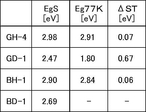
有機EL素子を以下のように作製し、評価した。 <Production and Evaluation of Organic EL Element>
An organic EL element was produced and evaluated as follows.
25mm×75mm×1.1mm厚のITO透明電極(陽極)付きガラス基板(ジオマティック社製)をイソプロピルアルコール中で超音波洗浄を5分間行なった後、UVオゾン洗浄を30分間行なった。ITOの膜厚は、130nmとした。
洗浄後の透明電極ライン付きガラス基板を真空蒸着装置の基板ホルダーに装着し、まず透明電極ラインが形成されている側の面上に透明電極を覆うようにして化合物HI-1を蒸着し、膜厚50nmの化合物HI-1膜を形成した。このHI-1膜は、正孔注入層として機能する。
このHI-1膜の成膜に続けて、化合物HT-1を蒸着し、HI-1膜上に膜厚60nmのHT-1膜を成膜した。このHT-1膜は、正孔輸送層として機能する。
このHT-1膜上に化合物GH-4(ホスト材料)および化合物GD-1(蛍光発光性ドーパント材料)を共蒸着し、膜厚30nmの発光層を成膜した。ドーパント材料濃度は、5質量%とした。
この発光層上に電子輸送性化合物であるET-1を蒸着し、膜厚25nmの電子輸送層を形成した。
この電子輸送層上にLiFを蒸着して、膜厚1nmのLiF膜を形成した。
このLiF膜上に金属Alを蒸着して、膜厚80nmの金属陰極を形成した。
このようにして、実施例1の有機EL素子を作製した。
実施例1の有機EL素子の素子構成を略式的に示すと、次のとおりである。
ITO(130)/HI-1(50)/HT-1(60)/GH-4:GD-1(30,5%)/ET-1(25)/LiF(1)/Al(80)
なお、括弧内の数字は、膜厚(単位:nm)を示す。また、同じく括弧内において、パーセント表示された数字は、発光層における蛍光光発光性ドーパント材料等のように、添加される成分の割合(質量%)を示す。 Example 1
A 25 mm × 75 mm × 1.1 mm thick glass substrate with ITO transparent electrode (anode) (manufactured by Geomatic) was ultrasonically cleaned in isopropyl alcohol for 5 minutes, and then UV ozone cleaning was performed for 30 minutes. The film thickness of ITO was 130 nm.
A glass substrate with a transparent electrode line after washing is mounted on a substrate holder of a vacuum vapor deposition apparatus, and first, compound HI-1 is vapor-deposited so as to cover the transparent electrode on the surface where the transparent electrode line is formed. A compound HI-1 film having a thickness of 50 nm was formed. This HI-1 film functions as a hole injection layer.
Subsequent to the formation of the HI-1 film, the compound HT-1 was evaporated, and an HT-1 film having a thickness of 60 nm was formed on the HI-1 film. This HT-1 film functions as a hole transport layer.
On this HT-1 film, compound GH-4 (host material) and compound GD-1 (fluorescent dopant material) were co-evaporated to form a light emitting layer having a thickness of 30 nm. The dopant material concentration was 5% by mass.
On this light emitting layer, ET-1 which is an electron transporting compound was vapor-deposited to form an electron transporting layer having a film thickness of 25 nm.
LiF was vapor-deposited on this electron transport layer to form a 1-nm thick LiF film.
Metal Al was vapor-deposited on this LiF film to form a metal cathode having a thickness of 80 nm.
Thus, the organic EL element of Example 1 was produced.
A device arrangement of the organic EL device of Example 1 is schematically shown as follows.
ITO (130) / HI-1 (50) / HT-1 (60) / GH-4: GD-1 (30,5%) / ET-1 (25) / LiF (1) / Al (80)
The numbers in parentheses indicate the film thickness (unit: nm). Similarly, in the parentheses, the number displayed as a percentage indicates the ratio (mass%) of the added component such as a fluorescent light-emitting dopant material in the light-emitting layer.
作製した有機EL素子について、駆動電圧、CIE1931色度、電流効率L/J、電力効率、外部量子効率EQE、及び遅延蛍光比率の評価を行った。遅延蛍光比率以外の各評価項目について、電流密度を1.00mA/cm2、又は10.00mA/cm2とした場合について行い、前者の場合を評価例1、後者の場合を評価例2とした。結果を表2に示す。 [Evaluation of organic EL elements]
About the produced organic EL element, drive voltage, CIE1931 chromaticity, current efficiency L / J, power efficiency, external quantum efficiency EQE, and delayed fluorescence ratio were evaluated. For each evaluation item other than the delayed fluorescence ratio, the current density was set to 1.00 mA / cm 2 or 10.00 mA / cm 2 , the former case being Evaluation Example 1, and the latter case being Evaluation Example 2. . The results are shown in Table 2.
電流密度が1.00mA/cm2、又は10.00mA/cm2となるようにITOとAlとの間に通電したときの電圧(単位:V)を計測した。 -Driving voltage The voltage (unit: V) when electricity was supplied between ITO and Al so that a current density might be set to 1.00 mA / cm < 2 > or 10.00 mA / cm < 2 > was measured.
電流密度が1.00mA/cm2、又は10.00mA/cm2となるように素子に電圧を印加した時のCIE1931色度座標(x、y)を分光放射輝度計CS-1000(コニカミノルタ社製)で計測した。 CIE1931 chromaticity CIE1931 chromaticity coordinates (x, y) when a voltage is applied to the element so that the current density is 1.00 mA / cm 2 or 10.00 mA / cm 2 is a spectral radiance meter CS-1000 (Measured by Konica Minolta).
電流密度が1.00mA/cm2、又は10.00mA/cm2となるように素子に電圧を印加した時の分光放射輝度スペクトルを上記分光放射輝度計で計測し、得られた分光放射輝度スペクトルから、電流効率(単位:cd/A)、及び電力効率η(単位:lm/W)を算出した。 ・ Current efficiency L / J and power efficiency η
The spectral radiance spectrum obtained by measuring the spectral radiance spectrum when a voltage was applied to the device so that the current density was 1.00 mA / cm 2 or 10.00 mA / cm 2 was obtained. From these, current efficiency (unit: cd / A) and power efficiency η (unit: lm / W) were calculated.
得られた上記分光放射輝度スペクトルから主ピーク波長λpを求めた。 ・ Main peak wavelength λ p
The main peak wavelength λ p was determined from the obtained spectral radiance spectrum.
得られた上記分光放射輝度スペクトルから、ランバシアン放射を行なったと仮定し外部量子効率EQE(単位:%)を算出した。 ・ External quantum efficiency EQE
From the obtained spectral radiance spectrum, the external quantum efficiency EQE (unit:%) was calculated on the assumption that Lambtian radiation was performed.

パルスジェネレータ(アジレント社製8114A)から出力した電圧パルス波形(パルス幅:500マイクロ秒、周波数:20Hz、電圧:0.1~100mA/cm2相当の電圧を印加し、EL発光を光電子増倍管(浜松ホトニクス社製R928)に入力し、パルス電圧波形とEL発光とを同期させてオシロスコープ(テクトロニクス社製2440)に取り込んで過渡EL波形を得た。これを最小二乗法により10-5秒までの値を用いて直線へフィッティングし、遅延蛍光比率を決定した。
実施例1の有機EL素子に対して、室温下、0.14mA/cm2で通電した時の過渡EL波形を、前述の図6Aに示した。時刻約3×10-8秒のところでパルス電圧を除去した。
電圧除去時点を原点にとり、電圧除去後、1.5×10⁻⁵秒までの光強度の平方根の逆数をプロットしたグラフが、前述の図6Bのグラフである。このグラフから求めた実施例1の有機EL素子における遅延蛍光比率は、41%であった。この遅延蛍光比率の値は、TTF比率の理論値限界37.5%を超えるものであった。
また、図6Aの図から、1μsにおける残存強度比を読み取ったところ、39.8%であった。 -Delayed fluorescence ratio Voltage pulse waveform output from a pulse generator (Agilent 8114A) (pulse width: 500 microseconds, frequency: 20 Hz, voltage: voltage corresponding to 0.1 to 100 mA / cm 2 is applied to emit EL light) It was input into a photomultiplier tube (R928 manufactured by Hamamatsu Photonics), and the pulse voltage waveform and EL light emission were synchronized and taken in an oscilloscope (Tektronix 2440) to obtain a transient EL waveform. Fitting to a straight line using values up to -5 seconds, the delayed fluorescence ratio was determined.
The transient EL waveform when the organic EL element of Example 1 is energized at 0.14 mA / cm 2 at room temperature is shown in FIG. 6A described above. The pulse voltage was removed at about 3 × 10 −8 seconds.
The graph of FIG. 6B described above is a graph in which the reciprocal of the square root of the light intensity up to 1.5 × 10 −5 seconds after the voltage removal is taken as the origin at the time of voltage removal. The delayed fluorescence ratio in the organic EL device of Example 1 obtained from this graph was 41%. The value of the delayed fluorescence ratio exceeded the theoretical limit of 37.5% of the TTF ratio.
Moreover, when the residual intensity | strength ratio in 1 microsecond was read from the figure of FIG. 6A, it was 39.8%.
実施例1の有機EL素子について、電流密度を変化させた場合の電流効率を測定した。図9に、電流効率及びの関係を示すグラフとして測定結果を示す。
図9に示されているように、電流密度が0.01mA/cm2のときよりも、1mA/cm2~10mA/cm2の電流密度領域におけるときの方が、電流効率が高くなった。 -Relationship between current efficiency and current density About the organic EL element of Example 1, the current efficiency at the time of changing a current density was measured. FIG. 9 shows the measurement results as a graph showing the relationship between the current efficiency and the current efficiency.
As shown in Figure 9, than when the current density is 0.01 mA / cm 2, is more time at a current density region of 1mA /
25mm×75mm×1.1mm厚のITO透明電極(陽極)付きガラス基板(ジオマティック社製)をイソプロピルアルコール中で超音波洗浄を5分間行なった後、UVオゾン洗浄を30分間行なった。ITOの膜厚は、70nmとした。
洗浄後の透明電極ライン付きガラス基板を真空蒸着装置の基板ホルダーに装着し、まず透明電極ラインが形成されている側の面上に透明電極を覆うようにして化合物HI-2を蒸着し、膜厚5nmの化合物HI-2膜を形成した。このHI-2膜は、正孔注入層として機能する。
このHI-2膜の成膜に続けて、化合物HT-2を蒸着し、HI-2膜上に膜厚125nmのHT-2膜を成膜した。このHT-2膜の成膜に続けて、化合物HT-3を蒸着し、HT-2膜上に膜厚25nmのHT-3膜を成膜した。このHT-2、HT-3膜は、正孔輸送層として機能する。
このHT-3膜上に化合物BH-1(ホスト材料)および化合物BD-1(蛍光発光性ドーパント材料)を共蒸着し、膜厚25nmの発光層を成膜した。ドーパント材料濃度は、4質量%とした。
この発光層上に電子輸送性化合物であるET-2を蒸着し、膜厚5nmの正孔阻止層を形成した。
この正孔阻止層上にET-3およびLiqを共蒸着して、膜厚20nmの電子輸送膜を形成した。ET-3およびLiqの濃度比は50質量%:50質量%とした。
この電子輸送層上にLiqを蒸着し、膜厚1nmのLiq層を形成した。
このLiq膜上に金属Alを蒸着して、膜厚80nmの金属陰極を形成した。
このようにして、実施例2の有機EL素子を作製した。
実施例2の有機EL素子の素子構成を略式的に示すと、次のとおりである。
ITO(70)/HI-2(5)/HT-2(125)/ HT-3(25)/BH-1:BD-1(25,4%)/ET-2(5)/ ET-3:Liq(20,50%)/Liq(1)/Al(80)
なお、括弧内の数字は、膜厚(単位:nm)を示す。また、同じく括弧内において、パーセント表示された数字は、BD-1、Liqの割合(質量%)を示す。 (Example 2)
A 25 mm × 75 mm × 1.1 mm thick glass substrate with ITO transparent electrode (anode) (manufactured by Geomatic) was ultrasonically cleaned in isopropyl alcohol for 5 minutes, and then UV ozone cleaning was performed for 30 minutes. The film thickness of ITO was 70 nm.
A glass substrate with a transparent electrode line after washing is mounted on a substrate holder of a vacuum deposition apparatus, and firstly compound HI-2 is vapor-deposited so as to cover the transparent electrode on the surface where the transparent electrode line is formed. A compound HI-2 film having a thickness of 5 nm was formed. This HI-2 film functions as a hole injection layer.
Subsequent to the formation of the HI-2 film, the compound HT-2 was vapor-deposited to form an HT-2 film having a thickness of 125 nm on the HI-2 film. Following the formation of the HT-2 film, the compound HT-3 was vapor-deposited to form a HT-3 film having a thickness of 25 nm on the HT-2 film. The HT-2 and HT-3 films function as a hole transport layer.
On this HT-3 film, compound BH-1 (host material) and compound BD-1 (fluorescent dopant material) were co-evaporated to form a light-emitting layer having a thickness of 25 nm. The dopant material concentration was 4% by mass.
ET-2, which is an electron transporting compound, was vapor-deposited on this light emitting layer to form a hole blocking layer having a thickness of 5 nm.
ET-3 and Liq were co-deposited on this hole blocking layer to form an electron transport film having a thickness of 20 nm. The concentration ratio of ET-3 and Liq was 50% by mass: 50% by mass.
Liq was vapor-deposited on this electron transport layer to form a Liq layer having a thickness of 1 nm.
Metal Al was vapor-deposited on this Liq film to form a metal cathode having a thickness of 80 nm.
Thus, the organic EL element of Example 2 was produced.
A device arrangement of the organic EL device of Example 2 is schematically shown as follows.
ITO (70) / HI-2 (5) / HT-2 (125) / HT-3 (25) / BH-1: BD-1 (25,4%) / ET-2 (5) / ET-3 : Liq (20,50%) / Liq (1) / Al (80)
The numbers in parentheses indicate the film thickness (unit: nm). Also, in the parentheses, the number displayed as a percentage indicates the ratio (mass%) of BD-1 and Liq.
作製した有機EL素子について、駆動電圧、CIE1931色度、電流効率L/J、電力効率、外部量子効率EQE、及び遅延蛍光比率の評価を行った。遅延蛍光比率以外の各評価項目について、電流密度を1.00mA/cm2とした場合について実施例1と同様の方法で行い、評価例3とした。結果を表3に示す。 [Evaluation of organic EL elements]
About the produced organic EL element, drive voltage, CIE1931 chromaticity, current efficiency L / J, power efficiency, external quantum efficiency EQE, and delayed fluorescence ratio were evaluated. With respect to each evaluation item other than the delayed fluorescence ratio, the case where the current density was set to 1.00 mA / cm 2 was performed in the same manner as in Example 1 and was set as Evaluation Example 3. The results are shown in Table 3.
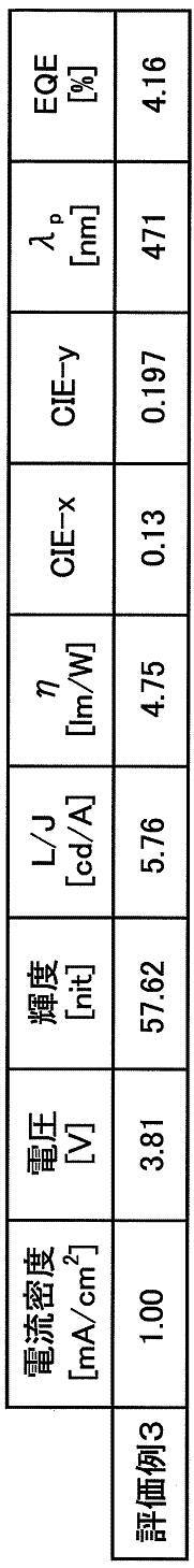
実施例1と同様の方法で、過渡EL波形を得た。これを最小二乗法により10-5秒までの値を用いて直線へフィッティングし、解析して遅延蛍光比率を決定した。
実施例2の有機EL素子に対して、室温下、1.00mA/cm2で通電した時の過渡EL波形を、図10に示した。時刻約3×10-8秒のところでパルス電圧を除去した。
電圧除去時点を原点にとり、実施例1と同様にして、電圧除去後、1.0×10⁻⁵秒までの光強度の平方根の逆数をプロットしたグラフを作成し、このグラフから遅延蛍光比率を求めた。実施例2の有機EL素子における遅延蛍光比率は、38.7%であった。この遅延蛍光比率の値は、TTF比率の理論値限界37.5%を超えるものであった。
・1μsにおける残存強度比
また、図10から、1μsにおける残存強度比を読み取ったところ、36.3%であった。 -Delayed fluorescence ratio A transient EL waveform was obtained in the same manner as in Example 1. This was fitted to a straight line using values up to 10 −5 seconds by the method of least squares and analyzed to determine the delayed fluorescence ratio.
FIG. 10 shows a transient EL waveform when the organic EL element of Example 2 is energized at 1.00 mA / cm 2 at room temperature. The pulse voltage was removed at about 3 × 10 −8 seconds.
Taking the time point of voltage removal as the origin, a graph plotting the reciprocal of the square root of the light intensity up to 1.0 × 10 −5 seconds after voltage removal was created in the same manner as in Example 1, and the delayed fluorescence ratio was calculated from this graph. Asked. The delayed fluorescence ratio in the organic EL device of Example 2 was 38.7%. The value of the delayed fluorescence ratio exceeded the theoretical limit of 37.5% of the TTF ratio.
-Residual intensity ratio in 1 microsecond Moreover, when the residual intensity ratio in 1 microsecond was read from FIG. 10, it was 36.3%.
ここで、非特許文献1に記載された有機EL素子を参考例として挙げ、実施例1の有機EL素子の素子構成との比較を行う。
この参考例の有機EL素子の構成は、実施例1の略式的表示に倣って示すと、次のとおりである。ITO(110)/NPD(40)/m-CP(10)/m-CP:PIC-TRZ(20,6%)/BP4mPy(40)/LiF(0.8)/Al(70)
参考例の素子に使用された化合物を以下に示す。 (Reference example)
Here, the organic EL element described in
The structure of the organic EL element of this reference example is as follows, following the schematic display of Example 1. ITO (110) / NPD (40) / m-CP (10) / m-CP: PIC-TRZ (20,6%) / BP4mPy (40) / LiF (0.8) / Al (70)
The compounds used in the device of the reference example are shown below.

2…基板
3…陽極
4…陰極
5…発光層
6…正孔注入層
7…正孔輸送層
8…電子輸送層
9…電子注入層
10…有機化合物層 DESCRIPTION OF
Claims (6)
- 一対の電極間に有機化合物層を備える有機エレクトロルミネッセンス素子であって、
前記有機化合物層は、第一の材料と第二の材料とを含む発光層を有し、
前記第二の材料は、蛍光発光を示す材料であり、
前記第一の材料の一重項エネルギーEgS(H)と前記第二の材料の一重項エネルギーEgS(D)とが、下記数式(1)の関係を満たし、
前記第一の材料は、前記一重項エネルギーEgS(H)と、77[K]におけるエネルギーギャップEg77K(H)との差ΔST(H)が、下記数式(2)の関係を満たす
ことを特徴とする有機エレクトロルミネッセンス素子。
[数1]
EgS(H)>EgS(D) …(1)
[数2]
ΔST(H)=EgS(H)-Eg77K(H)<0.3[eV]…(2) An organic electroluminescence device comprising an organic compound layer between a pair of electrodes,
The organic compound layer has a light emitting layer including a first material and a second material,
The second material is a material that exhibits fluorescence,
The singlet energy EgS (H) of the first material and the singlet energy EgS (D) of the second material satisfy the relationship of the following formula (1):
In the first material, the difference ΔST (H) between the singlet energy EgS (H) and the energy gap Eg 77K (H) at 77 [K] satisfies the relationship of the following formula (2). An organic electroluminescence element.
[Equation 1]
EgS (H)> EgS (D) (1)
[Equation 2]
ΔST (H) = EgS (H) −Eg 77K (H) <0.3 [eV] (2) - 請求項1に記載の有機エレクトロルミネッセンス素子において、
遅延蛍光比率が37.5%より大きい
ことを特徴とする有機エレクトロルミネッセンス素子。 The organic electroluminescent device according to claim 1,
An organic electroluminescence device having a delayed fluorescence ratio of greater than 37.5%. - 請求項1または請求項2に記載の有機エレクトロルミネッセンス素子において、
過渡EL測定における電圧除去後1μs経過後の残存強度比が36.0%より大きい
ことを特徴とする有機エレクトロルミネッセンス素子。 In the organic electroluminescent element according to claim 1 or 2,
An organic electroluminescence device, wherein a residual intensity ratio after 1 μs has elapsed after voltage removal in transient EL measurement is greater than 36.0%. - 請求項1から請求項3のいずれか一項に記載の有機エレクトロルミネッセンス素子において、
前記第一の材料のフォトルミネッセンススペクトルの半値幅が50nm以上である
ことを特徴とする有機エレクトロルミネッセンス素子。 In the organic electroluminescent element according to any one of claims 1 to 3,
The organic electroluminescent element characterized by the half-value width of the photoluminescence spectrum of said 1st material being 50 nm or more. - 請求項1から請求項3のいずれか一項に記載の有機エレクトロルミネッセンス素子において、
前記第一の材料のフォトルミネッセンススペクトルの半値幅が75nm以上である
ことを特徴とする有機エレクトロルミネッセンス素子。 In the organic electroluminescent element according to any one of claims 1 to 3,
The organic electroluminescent element characterized by the half-value width of the photoluminescence spectrum of said 1st material being 75 nm or more. - 請求項1から請求項5のいずれか一項に記載の有機エレクトロルミネッセンス素子において、
前記第一の材料の77[K]におけるエネルギーギャップEg77K(H)と、前記第二の材料の77[K]におけるエネルギーギャップEg77K(D)との差ΔTが、下記数式(3)の関係を満たす
ことを特徴とする有機エレクトロルミネッセンス素子。
[数3]
ΔT=Eg77K(H)―Eg77K(D)≧0.6[eV] …(3) In the organic electroluminescent element according to any one of claims 1 to 5,
The difference ΔT between the energy gap Eg 77K (H) at 77 [K] of the first material and the energy gap Eg 77K (D) at 77 [K] of the second material is expressed by the following formula (3). An organic electroluminescence device characterized by satisfying the relationship.
[Equation 3]
ΔT = Eg 77K (H) −Eg 77K (D) ≧ 0.6 [eV] (3)
Priority Applications (6)
| Application Number | Priority Date | Filing Date | Title |
|---|---|---|---|
| EP12762893.1A EP2690681B1 (en) | 2011-03-25 | 2012-03-23 | Organic electroluminescent element |
| JP2013507516A JP5889280B2 (en) | 2011-03-25 | 2012-03-23 | Organic electroluminescence device |
| KR1020137024878A KR101650996B1 (en) | 2011-03-25 | 2012-03-23 | Organic electroluminescent element |
| CN201280013486.1A CN103443949B9 (en) | 2011-03-25 | 2012-03-23 | Organic electroluminescent device |
| EP19191788.9A EP3598520A1 (en) | 2011-03-25 | 2012-03-23 | Organic electroluminescent element |
| KR1020167022479A KR102018418B1 (en) | 2011-03-25 | 2012-03-23 | Organic electroluminescent element |
Applications Claiming Priority (2)
| Application Number | Priority Date | Filing Date | Title |
|---|---|---|---|
| JP2011068758 | 2011-03-25 | ||
| JP2011-068758 | 2011-03-25 |
Publications (1)
| Publication Number | Publication Date |
|---|---|
| WO2012133188A1 true WO2012133188A1 (en) | 2012-10-04 |
Family
ID=46926281
Family Applications (1)
| Application Number | Title | Priority Date | Filing Date |
|---|---|---|---|
| PCT/JP2012/057520 WO2012133188A1 (en) | 2011-03-25 | 2012-03-23 | Organic electroluminescent element |
Country Status (7)
| Country | Link |
|---|---|
| US (4) | US8643268B2 (en) |
| EP (2) | EP3598520A1 (en) |
| JP (1) | JP5889280B2 (en) |
| KR (2) | KR102018418B1 (en) |
| CN (1) | CN105762279B (en) |
| TW (2) | TWI552406B (en) |
| WO (1) | WO2012133188A1 (en) |
Cited By (57)
| Publication number | Priority date | Publication date | Assignee | Title |
|---|---|---|---|---|
| WO2013172255A1 (en) * | 2012-05-17 | 2013-11-21 | 国立大学法人九州大学 | Compound, light emitting material, and organic light emitting element |
| WO2013180241A1 (en) * | 2012-06-01 | 2013-12-05 | 出光興産株式会社 | Organic electroluminescence element and material for organic electroluminescence element |
| JP2013258402A (en) * | 2012-05-18 | 2013-12-26 | Semiconductor Energy Lab Co Ltd | Light-emitting element, light-emitting device, display, electronic apparatus, and lighting device |
| WO2014013947A1 (en) * | 2012-07-20 | 2014-01-23 | 出光興産株式会社 | Organic electroluminescent element |
| KR20140018133A (en) * | 2012-08-03 | 2014-02-12 | 가부시키가이샤 한도오따이 에네루기 켄큐쇼 | Light-emitting element |
| WO2014092083A1 (en) * | 2012-12-10 | 2014-06-19 | 出光興産株式会社 | Organic electroluminescent element |
| WO2014104346A1 (en) * | 2012-12-28 | 2014-07-03 | 出光興産株式会社 | Organic electroluminescent element |
| WO2014104315A1 (en) * | 2012-12-28 | 2014-07-03 | 出光興産株式会社 | Organic electroluminescent element |
| WO2014109274A1 (en) * | 2013-01-10 | 2014-07-17 | Semiconductor Energy Laboratory Co., Ltd. | Light-emitting element, light-emitting device, electronic device, and lighting device |
| JP2014182898A (en) * | 2013-03-18 | 2014-09-29 | Idemitsu Kosan Co Ltd | Manufacturing method of organic electroluminescent element, organic electroluminescent element, and electronic apparatus |
| WO2014157619A1 (en) * | 2013-03-29 | 2014-10-02 | 国立大学法人九州大学 | Organic electroluminescent element |
| WO2014157610A1 (en) | 2013-03-29 | 2014-10-02 | コニカミノルタ株式会社 | Organic electroluminescent element, lighting device, display device, light-emitting thin film and composition for organic electroluminescent element, and light-emitting method |
| KR20150002534A (en) * | 2013-06-28 | 2015-01-07 | 가부시키가이샤 한도오따이 에네루기 켄큐쇼 | Method for fabricating light-emitting element and light-emitting element |
| JP5669163B1 (en) * | 2013-08-14 | 2015-02-12 | 国立大学法人九州大学 | Organic electroluminescence device |
| JP2015037138A (en) * | 2013-08-14 | 2015-02-23 | コニカミノルタ株式会社 | Organic electroluminescence element, metal complex for organic electroluminescence element, display device, and illumination device |
| JP2015038941A (en) * | 2013-08-19 | 2015-02-26 | コニカミノルタ株式会社 | Organic electroluminescent element, fluorescent emission compound used therefor, illumination device with the organic electroluminescent element and display device |
| JP2015053476A (en) * | 2013-07-30 | 2015-03-19 | 出光興産株式会社 | Organic electroluminescent element and electronic apparatus |
| JP2015065225A (en) * | 2013-09-24 | 2015-04-09 | 日本放送協会 | Organic electroluminescent element, and display device and lighting device using the same |
| JP2015106659A (en) * | 2013-11-29 | 2015-06-08 | 出光興産株式会社 | Organic electroluminescent element and electronic device |
| WO2015098975A1 (en) | 2013-12-26 | 2015-07-02 | 出光興産株式会社 | Organic electroluminescent element and electronic device |
| WO2015198987A1 (en) * | 2014-06-26 | 2015-12-30 | 出光興産株式会社 | Organic electroluminescent element, material for organic electroluminescent elements, and electronic device |
| WO2016010136A1 (en) * | 2014-07-18 | 2016-01-21 | 国立大学法人九州大学 | Organic light-emitting element |
| JP2016036022A (en) * | 2014-07-31 | 2016-03-17 | コニカミノルタ株式会社 | Organic electroluminescent device material, organic electroluminescent device, charge-transferable thin film, display and illuminating apparatus |
| KR20160045569A (en) * | 2014-10-17 | 2016-04-27 | 엘지디스플레이 주식회사 | Delayed fluorescence compound, and Organic light emitting diode device and Display device using the same |
| JP2016129262A (en) * | 2013-12-26 | 2016-07-14 | 出光興産株式会社 | Organic electroluminescent element and electronic device |
| JP2016522579A (en) * | 2013-06-06 | 2016-07-28 | メルク パテント ゲーエムベーハー | Organic electroluminescent device |
| WO2016125807A1 (en) * | 2015-02-06 | 2016-08-11 | 出光興産株式会社 | Organic electroluminescence element and electronic device |
| KR20160099644A (en) * | 2013-12-17 | 2016-08-22 | 베이징 비젼녹스 테크놀로지 컴퍼니 리미티드 | Organic electroluminescent device and method for manufacture thereof |
| KR20160113219A (en) | 2014-03-07 | 2016-09-28 | 코니카 미놀타 가부시키가이샤 | Organic electroluminescence element, display device, illumination device, and light-emitting composition |
| JP2017054972A (en) * | 2015-09-10 | 2017-03-16 | コニカミノルタ株式会社 | ORGANIC ELECTROLUMINESCENCE ELEMENT, DISPLAY DEVICE, LIGHTING DEVICE, π-CONJUGATED COMPOUND, AND LIGHT-EMITTING THIN FILM |
| JP2017509164A (en) * | 2014-03-13 | 2017-03-30 | メルク パテント ゲーエムベーハー | Organic electroluminescent device |
| KR20170085434A (en) | 2014-10-07 | 2017-07-24 | 이데미쓰 고산 가부시키가이샤 | Organic electroluminescence device and electronic device |
| JP2017197482A (en) * | 2016-04-28 | 2017-11-02 | コニカミノルタ株式会社 | π-CONJUGATED COMPOUND, ORGANIC ELECTROLUMINESCENT ELEMENT MATERIAL, LIGHT-EMITTING MATERIAL, CHARGE TRANSPORT MATERIAL, LUMINESCENT THIN FILM, ORGANIC ELECTROLUMINESCENT ELEMENT, DISPLAY DEVICE, AND LIGHTING DEVICE |
| KR101835934B1 (en) * | 2015-05-04 | 2018-03-08 | 단국대학교 산학협력단 | Oled having host exhibiting delayed fluorescence |
| JP2018519663A (en) * | 2015-06-16 | 2018-07-19 | 昆山国顕光電有限公司Kunshan Go−Visionox Opto−Electronics Co., Ltd. | Organic electroluminescence device and manufacturing method thereof |
| US10043982B2 (en) | 2013-04-26 | 2018-08-07 | Semiconductor Energy Laboratory Co., Ltd. | Light-emitting element, light-emitting device, display device, electronic device, and lighting device |
| JP2018524803A (en) * | 2015-06-03 | 2018-08-30 | ユー・ディー・シー アイルランド リミテッド | Highly efficient OLED device with extremely short decay time |
| JP2018524819A (en) * | 2015-07-23 | 2018-08-30 | メルク パテント ゲーエムベーハー | Phenyl derivatives substituted with at least two electron acceptors and at least two electron donors for use in organic electronic devices |
| JPWO2017115608A1 (en) * | 2015-12-28 | 2018-10-18 | コニカミノルタ株式会社 | π-conjugated compound, organic electroluminescence element material, light emitting material, charge transport material, light emitting thin film, organic electroluminescence element, display device and lighting device |
| US10141520B2 (en) | 2013-04-05 | 2018-11-27 | Konica Minolta, Inc. | Coating liquid for forming light emitting layer, organic electroluminescent element, method for manufacturing organic electroluminescent element, and lighting/display device |
| JP2019054261A (en) * | 2013-08-26 | 2019-04-04 | 株式会社半導体エネルギー研究所 | Light emitting device |
| WO2019115577A1 (en) | 2017-12-15 | 2019-06-20 | Merck Patent Gmbh | Substituted aromatic amines for use in organic electroluminescent devices |
| US10388888B2 (en) | 2014-12-29 | 2019-08-20 | University Court Of The University Of St Andrews | Light emitting electrochemical cells and compounds |
| WO2019225483A1 (en) * | 2018-05-21 | 2019-11-28 | 住友化学株式会社 | Composition for light-emitting element, method for producing composition for light-emitting element, method for evaluating composition for light-emitting element, light-emitting element, and method for producing light-emitting element |
| WO2020064582A1 (en) | 2018-09-24 | 2020-04-02 | Merck Patent Gmbh | Method for the production of a granular material |
| US10693095B2 (en) | 2014-08-29 | 2020-06-23 | Semiconductor Energy Laboratory Co., Ltd. | Light-emitting element, display device, electronic device, and lighting device |
| WO2020178230A1 (en) | 2019-03-04 | 2020-09-10 | Merck Patent Gmbh | Ligands for nano-sized materials |
| WO2021122868A1 (en) | 2019-12-19 | 2021-06-24 | Merck Patent Gmbh | Compounds for electronic devices |
| WO2021192159A1 (en) * | 2020-03-26 | 2021-09-30 | シャープ株式会社 | Light-emitting element and display device |
| WO2022129114A1 (en) | 2020-12-18 | 2022-06-23 | Merck Patent Gmbh | Nitrogenous compounds for organic electroluminescent devices |
| WO2022129116A1 (en) | 2020-12-18 | 2022-06-23 | Merck Patent Gmbh | Indolo[3.2.1-jk]carbazole-6-carbonitrile derivatives as blue fluorescent emitters for use in oleds |
| WO2022129113A1 (en) | 2020-12-18 | 2022-06-23 | Merck Patent Gmbh | Nitrogenous heteroaromatic compounds for organic electroluminescent devices |
| WO2022229234A1 (en) | 2021-04-30 | 2022-11-03 | Merck Patent Gmbh | Nitrogenous heterocyclic compounds for organic electroluminescent devices |
| WO2023041454A1 (en) | 2021-09-14 | 2023-03-23 | Merck Patent Gmbh | Boronic heterocyclic compounds for organic electroluminescent devices |
| WO2023072799A1 (en) | 2021-10-27 | 2023-05-04 | Merck Patent Gmbh | Boronic and nitrogenous heterocyclic compounds for organic electroluminescent devices |
| WO2023161167A1 (en) | 2022-02-23 | 2023-08-31 | Merck Patent Gmbh | Nitrogenous heterocycles for organic electroluminescent devices |
| WO2023161168A1 (en) | 2022-02-23 | 2023-08-31 | Merck Patent Gmbh | Aromatic hetreocycles for organic electroluminescent devices |
Families Citing this family (56)
| Publication number | Priority date | Publication date | Assignee | Title |
|---|---|---|---|---|
| US8847218B2 (en) * | 2011-01-20 | 2014-09-30 | Idemitsu Kosan Co., Ltd. | Organic electroluminescent element |
| EP3598520A1 (en) * | 2011-03-25 | 2020-01-22 | Idemitsu Kosan Co., Ltd | Organic electroluminescent element |
| DE102011089687A1 (en) * | 2011-12-22 | 2013-06-27 | Hartmut Yersin | Singlet Harvesting with special organic molecules without metal centers for opto-electronic devices |
| US10957870B2 (en) * | 2012-09-07 | 2021-03-23 | Universal Display Corporation | Organic light emitting device |
| JP6113993B2 (en) * | 2012-10-03 | 2017-04-12 | 出光興産株式会社 | Organic electroluminescence device |
| WO2014157433A1 (en) | 2013-03-26 | 2014-10-02 | Semiconductor Energy Laboratory Co., Ltd. | Light-emitting element, light-emitting device, electronic device, and lighting device |
| EP2984692B1 (en) * | 2013-04-08 | 2018-01-31 | Merck Patent GmbH | Organic electroluminescence device with thermally activated delayed fluorescence (tadf) material |
| EP2984691B1 (en) | 2013-04-08 | 2018-02-21 | Merck Patent GmbH | Organic light-emitting device having delayed fluorescence |
| JP6567499B2 (en) | 2013-04-08 | 2019-08-28 | メルク パテント ゲーエムベーハー | Organic electroluminescent device |
| WO2014185434A1 (en) * | 2013-05-16 | 2014-11-20 | Semiconductor Energy Laboratory Co., Ltd. | Light-emitting element, light-emitting device, electronic device, and lighting device |
| US9130182B2 (en) * | 2013-06-28 | 2015-09-08 | Semiconductor Energy Laboratory Co., Ltd. | Light-emitting element, lighting device, light-emitting device, and electronic device |
| JP6318155B2 (en) | 2013-08-01 | 2018-04-25 | 国立大学法人九州大学 | COMPOUND, LIGHT EMITTING MATERIAL AND ORGANIC LIGHT EMITTING DEVICE |
| US10734587B2 (en) | 2014-03-13 | 2020-08-04 | Merck Patent Gmbh | Formulations of luminescent compounds |
| US10461260B2 (en) * | 2014-06-03 | 2019-10-29 | Universal Display Corporation | Organic electroluminescent materials and devices |
| KR102031678B1 (en) | 2014-09-19 | 2019-10-14 | 이데미쓰 고산 가부시키가이샤 | Novel compound |
| CN111293226B (en) | 2014-09-30 | 2022-10-28 | 株式会社半导体能源研究所 | Light-emitting element, display device, electronic device, and lighting device |
| KR102409803B1 (en) | 2014-10-10 | 2022-06-17 | 가부시키가이샤 한도오따이 에네루기 켄큐쇼 | Light-emitting element, display device, electronic device, and lighting device |
| EP3010052B1 (en) * | 2014-10-17 | 2017-08-09 | LG Display Co., Ltd. | Delayed fluorescence compound, and organic light emitting diode and display device using the same |
| US10334685B2 (en) * | 2014-11-14 | 2019-06-25 | Board Of Supervisors Of Louisiana State University And Agricultural And Mechanical College | Carbon dot light emitting diodes |
| US9957280B2 (en) | 2014-12-15 | 2018-05-01 | Samsung Electronics Co., Ltd. | Luminescent compound and electroluminescent device exhibiting thermally activated delayed fluorescence |
| WO2016129536A1 (en) * | 2015-02-13 | 2016-08-18 | 出光興産株式会社 | Organic el light-emitting apparatus and electronic instrument |
| KR101706752B1 (en) * | 2015-02-17 | 2017-02-27 | 서울대학교산학협력단 | Organic light-emitting device comprising delayed fluorescent host, phosphorescent dopant and fluorescent dopant |
| TW202404148A (en) | 2015-03-09 | 2024-01-16 | 日商半導體能源研究所股份有限公司 | Light-emitting element, display device, electronic device, and lighting device |
| DE102015106941A1 (en) * | 2015-05-05 | 2016-11-10 | Osram Oled Gmbh | Organic emitter layer, organic light-emitting diode and use of heavy atoms in an organic emitter layer of an organic light-emitting diode |
| US11183645B2 (en) * | 2015-05-11 | 2021-11-23 | Nippon Hoso Kyokai | Organic thin film and method for manufacturing organic thin film, organic electroluminescence element, display device, illumination device, organic thin film solar cell, thin film transistor, and coating composition |
| US10651392B2 (en) | 2015-09-30 | 2020-05-12 | Samsung Electronics Co., Ltd. | Organic light-emitting device |
| JP6622569B2 (en) * | 2015-11-13 | 2019-12-18 | 株式会社ジャパンディスプレイ | Organic EL device |
| CN109196679B (en) * | 2015-12-01 | 2021-06-08 | 株式会社半导体能源研究所 | Light-emitting element, light-emitting device, electronic device, and lighting device |
| EP3389107A4 (en) | 2015-12-08 | 2019-08-14 | Idemitsu Kosan Co., Ltd | Organic el light emitting apparatus and electronic instrument |
| TWI594476B (en) * | 2015-12-11 | 2017-08-01 | 友達光電股份有限公司 | Organic fluorescent luminescent material and organic electro-luminescence device |
| CN106898709B (en) * | 2015-12-18 | 2019-03-29 | 昆山国显光电有限公司 | A kind of red phosphorescent organic electroluminescence device |
| US10604697B2 (en) * | 2016-02-19 | 2020-03-31 | Toray Industries, Inc. | Color conversion sheet, light source unit including the same, display, and lighting apparatus |
| CN105895819B (en) * | 2016-04-28 | 2018-07-06 | 京东方科技集团股份有限公司 | A kind of OLED device and preparation method thereof, OLED display panel |
| WO2018083801A1 (en) | 2016-11-07 | 2018-05-11 | 日立化成株式会社 | Organic electronic material, organic layer, organic electronic element, organic electroluminescent element, display element, illumination device, and display device |
| US10988447B2 (en) | 2016-06-30 | 2021-04-27 | Samsung Electronics Co., Ltd. | Bipyridine derivatives and their uses for organic light emitting diodes |
| US10665792B2 (en) * | 2016-08-24 | 2020-05-26 | Cynora Gmbh | Organic molecules for use in optoelectronic devices |
| CN109790086A (en) * | 2016-10-03 | 2019-05-21 | 出光兴产株式会社 | Compound, composition, organic electroluminescent element, and electronic device |
| KR102037816B1 (en) * | 2016-11-16 | 2019-10-29 | 삼성에스디아이 주식회사 | Organic optoelectronic device and display device |
| US10153445B2 (en) * | 2016-11-21 | 2018-12-11 | Universal Display Corporation | Organic electroluminescent materials and devices |
| US11637244B2 (en) * | 2016-12-21 | 2023-04-25 | Kyushu University, National University Corporation | Light-emitting material, compound, and organic light-emitting element |
| WO2018159694A1 (en) | 2017-03-02 | 2018-09-07 | 日立化成株式会社 | Organic electronic material and use of same |
| US10636977B2 (en) | 2017-04-14 | 2020-04-28 | Feng-wen Yen | Light emitting material for organic electroluminescence device |
| KR102515592B1 (en) | 2017-08-24 | 2023-03-30 | 삼성디스플레이 주식회사 | Compound including nitrogen and organic electroluminescence device including the same |
| CN109599493B (en) * | 2017-09-30 | 2021-06-29 | 昆山国显光电有限公司 | Organic electroluminescent device |
| JP7218348B2 (en) | 2018-03-07 | 2023-02-06 | 株式会社半導体エネルギー研究所 | Light-emitting elements, light-emitting devices, electronic devices and lighting devices |
| KR102477354B1 (en) * | 2018-03-29 | 2022-12-15 | 삼성전자주식회사 | Plasma processing apparatus including gas distribution plate |
| US20210057667A1 (en) * | 2018-05-11 | 2021-02-25 | Semiconductor Energy Laboratory Co., Ltd. | Light-emitting element, display device, electronic appliance, organic compound, and lighting device |
| US11063224B2 (en) * | 2018-05-30 | 2021-07-13 | Kunshan Go-Visionox Opto-Electronics Co., Ltd. | Organic electroluminescent device |
| KR102648402B1 (en) | 2018-06-12 | 2024-03-18 | 삼성디스플레이 주식회사 | Condensed-cyclic compound and organic light emitting device including the same |
| EP3844244B1 (en) * | 2018-08-28 | 2022-08-03 | Merck Patent GmbH | Materials for organic electroluminescent devices |
| KR102647025B1 (en) | 2018-12-28 | 2024-03-12 | 엘지디스플레이 주식회사 | Organic compounds having improved luminsecent properties, organic light emitting diode and organic light emitting device including the compounds |
| US11930653B2 (en) | 2019-02-06 | 2024-03-12 | Semiconductor Energy Laboratory Co., Ltd. | Light-emitting device, light-emitting appliance, display device, electronic appliance, and lighting device |
| CN110854279B (en) * | 2019-10-22 | 2021-06-01 | Tcl华星光电技术有限公司 | OLED display panel and display device |
| JP2021172603A (en) * | 2020-04-22 | 2021-11-01 | 出光興産株式会社 | Compound, material for organic electroluminescent device, organic electroluminescent device, and electronic apparatus |
| US20230345751A1 (en) | 2020-09-18 | 2023-10-26 | Samsung Display Co., Ltd. | Organic electroluminescent device |
| EP4223853A1 (en) | 2022-02-04 | 2023-08-09 | Samsung Display Co., Ltd. | Organic electroluminescent devices |
Citations (7)
| Publication number | Priority date | Publication date | Assignee | Title |
|---|---|---|---|---|
| WO2003080761A1 (en) * | 2002-03-25 | 2003-10-02 | Idemitsu Kosan Co., Ltd. | Material for organic electroluminescent element and organic electroluminescent element employing the same |
| WO2003080760A1 (en) | 2002-03-22 | 2003-10-02 | Idemitsu Kosan Co., Ltd. | Material for organic electroluminescent devices and organic electroluminescent devices made by using the same |
| JP2010180204A (en) | 2009-01-06 | 2010-08-19 | Fujifilm Corp | Charge transport material and organic electroluminescent device |
| WO2010134350A1 (en) | 2009-05-22 | 2010-11-25 | 出光興産株式会社 | Organic electroluminescent element |
| WO2010134352A1 (en) | 2009-05-22 | 2010-11-25 | 出光興産株式会社 | Organic electroluminescent element |
| WO2011070963A1 (en) * | 2009-12-07 | 2011-06-16 | 新日鐵化学株式会社 | Organic light-emitting material and organic light-emitting element |
| WO2011132683A1 (en) * | 2010-04-20 | 2011-10-27 | 出光興産株式会社 | Bis-carbazole derivative, material for organic electroluminescent element and organic electroluminescent element using same |
Family Cites Families (47)
| Publication number | Priority date | Publication date | Assignee | Title |
|---|---|---|---|---|
| JPS5821635B2 (en) | 1971-12-06 | 1983-05-02 | エリ− リリ− エンド カンパニ− | 3- Methyl -3- |
| JPH11307255A (en) | 1998-04-22 | 1999-11-05 | Matsushita Electric Ind Co Ltd | Organic electroluminecence element |
| US20030205696A1 (en) * | 2002-04-25 | 2003-11-06 | Canon Kabushiki Kaisha | Carbazole-based materials for guest-host electroluminescent systems |
| WO2004034751A1 (en) * | 2002-10-09 | 2004-04-22 | Idemitsu Kosan Co., Ltd. | Organic electroluminescent device |
| JP4287198B2 (en) * | 2002-11-18 | 2009-07-01 | 出光興産株式会社 | Organic electroluminescence device |
| CN100518424C (en) * | 2002-11-18 | 2009-07-22 | 出光兴产株式会社 | organic electroluminescent element |
| WO2004055921A2 (en) * | 2002-12-13 | 2004-07-01 | Philips Intellectual Property & Standards Gmbh | Organic electroluminescent component with triplet emitter complex |
| JP2004214180A (en) * | 2002-12-16 | 2004-07-29 | Canon Inc | Organic light-emitting element |
| JP2004241374A (en) | 2003-01-17 | 2004-08-26 | Sogo Pharmaceutical Co Ltd | Organic electroluminescent element |
| JP4188369B2 (en) | 2003-04-10 | 2008-11-26 | 出光興産株式会社 | Aromatic amine derivatives |
| JP4552436B2 (en) | 2003-12-24 | 2010-09-29 | コニカミノルタホールディングス株式会社 | Organic electroluminescence element, display device and lighting device |
| CN1934906A (en) | 2004-03-19 | 2007-03-21 | 出光兴产株式会社 | organic electroluminescent element |
| KR100573137B1 (en) | 2004-04-02 | 2006-04-24 | 삼성에스디아이 주식회사 | Fluorene-based compound and organic electroluminescent display device using the same |
| KR100787425B1 (en) | 2004-11-29 | 2007-12-26 | 삼성에스디아이 주식회사 | Phenylcarbazole-based compound and Organic electroluminescence display employing the same |
| JP2006024830A (en) | 2004-07-09 | 2006-01-26 | Sogo Pharmaceutical Co Ltd | Organic electroluminescent device |
| JP4541809B2 (en) | 2004-09-08 | 2010-09-08 | キヤノン株式会社 | Organic compound and organic light emitting device |
| US7597967B2 (en) * | 2004-12-17 | 2009-10-06 | Eastman Kodak Company | Phosphorescent OLEDs with exciton blocking layer |
| US7768194B2 (en) | 2005-06-01 | 2010-08-03 | The Trustees Of Princeton University | Fluorescent filtered electrophosphorescence |
| US7474048B2 (en) | 2005-06-01 | 2009-01-06 | The Trustees Of Princeton University | Fluorescent filtered electrophosphorescence |
| WO2007065550A1 (en) | 2005-12-08 | 2007-06-14 | Merck Patent Gmbh | Novel materials for organic electroluminescent devices |
| DE102005058557A1 (en) | 2005-12-08 | 2007-06-14 | Merck Patent Gmbh | Organic electroluminescent device |
| KR100752321B1 (en) * | 2005-12-23 | 2007-08-29 | 주식회사 두산 | White light emitting oragnic electroluminecent device |
| JP4388590B2 (en) | 2006-11-09 | 2009-12-24 | 新日鐵化学株式会社 | Compound for organic electroluminescence device and organic electroluminescence device |
| JP2007208289A (en) * | 2007-03-30 | 2007-08-16 | Idemitsu Kosan Co Ltd | Organic electroluminescent device |
| JP5481385B2 (en) * | 2007-11-15 | 2014-04-23 | 日東電工株式会社 | Light emitting device and light emitting composition |
| JP2009123976A (en) | 2007-11-16 | 2009-06-04 | Toyo Ink Mfg Co Ltd | Material for organic electroluminescent element, and organic electroluminescent element |
| KR100966885B1 (en) * | 2008-02-29 | 2010-06-30 | 다우어드밴스드디스플레이머티리얼 유한회사 | Novel organic electroluminescent compounds and organic electroluminescent device using the same |
| KR100946411B1 (en) | 2008-03-28 | 2010-03-09 | 다우어드밴스드디스플레이머티리얼 유한회사 | Novel organic electroluminescent compounds and organic electroluminescent device using the same |
| KR100964232B1 (en) | 2008-09-03 | 2010-06-17 | 삼성모바일디스플레이주식회사 | Silicon-containing compound and organic light emitting devide employing the same |
| JP2010114070A (en) | 2008-10-10 | 2010-05-20 | Canon Inc | White organic el element |
| JP2010114425A (en) | 2008-10-10 | 2010-05-20 | Canon Inc | Organic el display device |
| JP5448680B2 (en) | 2008-10-10 | 2014-03-19 | キヤノン株式会社 | Display device |
| JP2010114428A (en) | 2008-10-10 | 2010-05-20 | Canon Inc | Organic electroluminescent display device |
| EP2337785A1 (en) * | 2008-10-16 | 2011-06-29 | Solvay SA | N-phenyl carbazole-based host material for light-emitting diodes |
| DE102009023155A1 (en) * | 2009-05-29 | 2010-12-02 | Merck Patent Gmbh | Materials for organic electroluminescent devices |
| CN101740723B (en) | 2009-11-03 | 2011-09-21 | 电子科技大学 | Organic electroluminescent device and preparation method thereof |
| KR101506999B1 (en) * | 2009-11-03 | 2015-03-31 | 제일모직 주식회사 | Compound for organic photoelectric device and organic photoelectric device including the same |
| US8617720B2 (en) * | 2009-12-21 | 2013-12-31 | E I Du Pont De Nemours And Company | Electroactive composition and electronic device made with the composition |
| JP2011222831A (en) | 2010-04-12 | 2011-11-04 | Idemitsu Kosan Co Ltd | Organic electroluminescent element |
| KR101957527B1 (en) | 2010-06-24 | 2019-03-13 | 도레이 카부시키가이샤 | Light-emitting device material and light-emitting device |
| JP5594031B2 (en) | 2010-10-01 | 2014-09-24 | 東レ株式会社 | Light emitting device material and light emitting device |
| EP3598520A1 (en) * | 2011-03-25 | 2020-01-22 | Idemitsu Kosan Co., Ltd | Organic electroluminescent element |
| US9530969B2 (en) | 2011-12-05 | 2016-12-27 | Idemitsu Kosan Co., Ltd. | Material for organic electroluminescence device and organic electroluminescence device |
| CN103959503B (en) | 2011-12-05 | 2016-08-24 | 出光兴产株式会社 | Material for organic electroluminescent element and organic electroluminescent element |
| WO2013084885A1 (en) | 2011-12-05 | 2013-06-13 | 出光興産株式会社 | Organic electroluminescent element |
| JP5959970B2 (en) * | 2012-07-20 | 2016-08-02 | 出光興産株式会社 | Organic electroluminescence device |
| CN106104839B (en) * | 2014-03-13 | 2018-12-18 | 默克专利有限公司 | Organic electroluminescence device |
-
2012
- 2012-03-23 EP EP19191788.9A patent/EP3598520A1/en active Pending
- 2012-03-23 TW TW101110136A patent/TWI552406B/en active
- 2012-03-23 KR KR1020167022479A patent/KR102018418B1/en active IP Right Grant
- 2012-03-23 US US13/428,314 patent/US8643268B2/en active Active
- 2012-03-23 EP EP12762893.1A patent/EP2690681B1/en active Active
- 2012-03-23 CN CN201610200978.1A patent/CN105762279B/en active Active
- 2012-03-23 JP JP2013507516A patent/JP5889280B2/en active Active
- 2012-03-23 WO PCT/JP2012/057520 patent/WO2012133188A1/en active Application Filing
- 2012-03-23 TW TW105121552A patent/TW201638086A/en unknown
- 2012-03-23 KR KR1020137024878A patent/KR101650996B1/en active IP Right Grant
-
2013
- 2013-12-26 US US14/141,364 patent/US20140103329A1/en not_active Abandoned
-
2017
- 2017-02-01 US US15/422,054 patent/US10879482B2/en active Active
-
2020
- 2020-11-20 US US17/100,128 patent/US20210074941A1/en active Pending
Patent Citations (7)
| Publication number | Priority date | Publication date | Assignee | Title |
|---|---|---|---|---|
| WO2003080760A1 (en) | 2002-03-22 | 2003-10-02 | Idemitsu Kosan Co., Ltd. | Material for organic electroluminescent devices and organic electroluminescent devices made by using the same |
| WO2003080761A1 (en) * | 2002-03-25 | 2003-10-02 | Idemitsu Kosan Co., Ltd. | Material for organic electroluminescent element and organic electroluminescent element employing the same |
| JP2010180204A (en) | 2009-01-06 | 2010-08-19 | Fujifilm Corp | Charge transport material and organic electroluminescent device |
| WO2010134350A1 (en) | 2009-05-22 | 2010-11-25 | 出光興産株式会社 | Organic electroluminescent element |
| WO2010134352A1 (en) | 2009-05-22 | 2010-11-25 | 出光興産株式会社 | Organic electroluminescent element |
| WO2011070963A1 (en) * | 2009-12-07 | 2011-06-16 | 新日鐵化学株式会社 | Organic light-emitting material and organic light-emitting element |
| WO2011132683A1 (en) * | 2010-04-20 | 2011-10-27 | 出光興産株式会社 | Bis-carbazole derivative, material for organic electroluminescent element and organic electroluminescent element using same |
Non-Patent Citations (13)
| Title |
|---|
| "Hikarikagaku no Sekai", 1993, pages: 50 |
| "Organic EL Symposium", 17 June 2010, article "Expression of Highly-Efficient Thermally-Activated Delayed-Fluorescence and Application thereof to OLED", pages: 11 - 12 |
| "Organic EL Symposium", vol. S2-5, pages: II-12 |
| "Organic Photochemical Reaction Theory", 1973, TOKYO KAGAKU DOJIN CO., LTD. |
| D. YOKOYAMA ET AL., APPL. PHYS. LETT., vol. 93, 2008, pages 173302 |
| D. YOKOYAMA ET AL., APPL. PHYS. LETT., vol. 95, 2009, pages 243303 |
| D. YOKOYAMA ET AL., ORG. ELECTRON., vol. 10, 2009, pages 127 - 137 |
| ENDO ET AL.: "Efficient up-conversion of triplet excitons into a singlet state and its application for organic light emitting diodes", APPLIED PHYSICS LETTERS, vol. 98, no. 8, 24 February 2011 (2011-02-24), pages 083302 - 1-3, XP012140060 * |
| J. KANG ET AL., INTERNATIONAL JOURNAL OF POLYMER SCIENCE, vol. 2010 |
| M. KASHA ET AL., PURE AND APPLIED CHEMISTRY, vol. 11, 1965, pages 371 |
| S. DAS ET AL., J. PHYS. CHEM. B., vol. 103, 1999, pages 209 |
| S. M. BACHILO ET AL., J. PHYS. CHEM. A, vol. 104, 2000, pages 7711 |
| See also references of EP2690681A4 |
Cited By (135)
| Publication number | Priority date | Publication date | Assignee | Title |
|---|---|---|---|---|
| US9660199B2 (en) | 2012-05-17 | 2017-05-23 | Kyulux, Inc. | Compound, light-emitting material, and organic light-emitting device |
| WO2013172255A1 (en) * | 2012-05-17 | 2013-11-21 | 国立大学法人九州大学 | Compound, light emitting material, and organic light emitting element |
| JP2013258402A (en) * | 2012-05-18 | 2013-12-26 | Semiconductor Energy Lab Co Ltd | Light-emitting element, light-emitting device, display, electronic apparatus, and lighting device |
| US9099658B2 (en) | 2012-06-01 | 2015-08-04 | Idemitsu Kosan Co., Ltd. | Organic electroluminescence device |
| WO2013180241A1 (en) * | 2012-06-01 | 2013-12-05 | 出光興産株式会社 | Organic electroluminescence element and material for organic electroluminescence element |
| USRE49343E1 (en) | 2012-06-01 | 2022-12-20 | Idemitsu Kosan Co., Ltd. | Organic electroluminescence device |
| WO2014013947A1 (en) * | 2012-07-20 | 2014-01-23 | 出光興産株式会社 | Organic electroluminescent element |
| US10461264B2 (en) | 2012-07-20 | 2019-10-29 | Idemitsu Kosan Co., Ltd. | Organic electroluminescent element |
| US10930860B2 (en) | 2012-07-20 | 2021-02-23 | Idemitsu Kosan Co., Ltd. | Organic electroluminescent element |
| US10032998B2 (en) | 2012-07-20 | 2018-07-24 | Idemitsu Kosan Co., Ltd. | Organic electroluminescent element |
| US9608209B2 (en) | 2012-07-20 | 2017-03-28 | Idemitsu Kosan Co., Ltd. | Organic electroluminescent element |
| US9219242B2 (en) | 2012-07-20 | 2015-12-22 | Idemitsu Kosan Co., Ltd. | Organic electroluminescent element |
| JP7030927B2 (en) | 2012-08-03 | 2022-03-07 | 株式会社半導体エネルギー研究所 | Light emitting elements, lighting devices, light emitting devices and electronic devices |
| JP2021022744A (en) * | 2012-08-03 | 2021-02-18 | 株式会社半導体エネルギー研究所 | Light-emitting element, lighting device, light-emitting device and electronic device |
| JP2020141138A (en) * | 2012-08-03 | 2020-09-03 | 株式会社半導体エネルギー研究所 | Light-emitting device |
| US10644254B2 (en) | 2012-08-03 | 2020-05-05 | Semiconductor Energy Laboratory Co., Ltd. | Light-emitting element |
| US9947885B2 (en) | 2012-08-03 | 2018-04-17 | Semiconductor Energy Laboratory Co., Ltd. | Light-emitting element |
| JP2022065158A (en) * | 2012-08-03 | 2022-04-26 | 株式会社半導体エネルギー研究所 | Light-emitting element, illumination device, light-emitting device, and electronic apparatus |
| US10734594B2 (en) | 2012-08-03 | 2020-08-04 | Semiconductor Energy Laboratory Co., Ltd. | Light-emitting element |
| US10505132B2 (en) | 2012-08-03 | 2019-12-10 | Semiconductor Energy Laboratory Co., Ltd. | Light-emitting element |
| KR102208540B1 (en) * | 2012-08-03 | 2021-01-28 | 가부시키가이샤 한도오따이 에네루기 켄큐쇼 | Light-emitting element |
| KR20140018133A (en) * | 2012-08-03 | 2014-02-12 | 가부시키가이샤 한도오따이 에네루기 켄큐쇼 | Light-emitting element |
| JP2018152589A (en) * | 2012-08-03 | 2018-09-27 | 株式会社半導体エネルギー研究所 | Light emission method, light-emitting element, illuminating device, light-emitting device and electronic equipment |
| JP7202491B2 (en) | 2012-08-03 | 2023-01-11 | 株式会社半導体エネルギー研究所 | Light-emitting elements, lighting devices, light-emitting devices, and electronic devices |
| JP2014045179A (en) * | 2012-08-03 | 2014-03-13 | Semiconductor Energy Lab Co Ltd | Light-emitting element |
| JP2017195389A (en) * | 2012-08-03 | 2017-10-26 | 株式会社半導体エネルギー研究所 | Light-emitting element, illuminating device, light-emitting device, and electronic equipment |
| US9559313B2 (en) | 2012-08-03 | 2017-01-31 | Semiconductor Energy Laboratory Co., Ltd. | Light-emitting element |
| KR20180133352A (en) * | 2012-08-03 | 2018-12-14 | 가부시키가이샤 한도오따이 에네루기 켄큐쇼 | Light-emitting element |
| JP2016006906A (en) * | 2012-08-03 | 2016-01-14 | 株式会社半導体エネルギー研究所 | Light emitting element |
| JP2019054257A (en) * | 2012-08-03 | 2019-04-04 | 株式会社半導体エネルギー研究所 | Light-emitting device and light emitting method |
| JP2019041114A (en) * | 2012-08-03 | 2019-03-14 | 株式会社半導体エネルギー研究所 | Light emitting device |
| US9276228B2 (en) | 2012-08-03 | 2016-03-01 | Semiconductor Energy Laboratory Co., Ltd. | Light-emitting element |
| US11355722B2 (en) | 2012-08-03 | 2022-06-07 | Semiconductor Energy Laboratory Co., Ltd. | Light-emitting element |
| US11730007B2 (en) | 2012-08-03 | 2023-08-15 | Semiconductor Energy Laboratory Co., Ltd. | Light-emitting element |
| US10297761B2 (en) | 2012-12-10 | 2019-05-21 | Idemitsu Kosan Co., Ltd. | Organic electroluminescent element |
| WO2014092083A1 (en) * | 2012-12-10 | 2014-06-19 | 出光興産株式会社 | Organic electroluminescent element |
| US10186665B2 (en) | 2012-12-28 | 2019-01-22 | Idemitsu Kosan Co., Ltd. | Organic electroluminescent element |
| JPWO2014104315A1 (en) * | 2012-12-28 | 2017-01-19 | 出光興産株式会社 | Organic electroluminescence device |
| WO2014104315A1 (en) * | 2012-12-28 | 2014-07-03 | 出光興産株式会社 | Organic electroluminescent element |
| WO2014104346A1 (en) * | 2012-12-28 | 2014-07-03 | 出光興産株式会社 | Organic electroluminescent element |
| US9882144B2 (en) | 2012-12-28 | 2018-01-30 | Idemitsu Kosan Co., Ltd. | Organic electroluminescent element |
| US9391290B2 (en) | 2013-01-10 | 2016-07-12 | Semiconductor Energy Laboratory Co., Ltd. | Light-emitting device comprising an organic compound |
| US9634267B2 (en) | 2013-01-10 | 2017-04-25 | Semiconductor Energy Laboratory Co., Ltd. | Light-emitting element, light-emitting device, electronic device, and lighting device |
| WO2014109274A1 (en) * | 2013-01-10 | 2014-07-17 | Semiconductor Energy Laboratory Co., Ltd. | Light-emitting element, light-emitting device, electronic device, and lighting device |
| US9935286B2 (en) | 2013-01-10 | 2018-04-03 | Semiconductor Energy Laboratory Co., Ltd. | Light-emitting element, light-emitting device, electronic device, and lighting device |
| JP2014182898A (en) * | 2013-03-18 | 2014-09-29 | Idemitsu Kosan Co Ltd | Manufacturing method of organic electroluminescent element, organic electroluminescent element, and electronic apparatus |
| JPWO2014157619A1 (en) * | 2013-03-29 | 2017-02-16 | 国立大学法人九州大学 | Organic electroluminescence device |
| US10600983B2 (en) | 2013-03-29 | 2020-03-24 | Kyulux, Inc. | Organic electroluminescent device comprising delayed fluorescent materials |
| WO2014157619A1 (en) * | 2013-03-29 | 2014-10-02 | 国立大学法人九州大学 | Organic electroluminescent element |
| CN105074951A (en) * | 2013-03-29 | 2015-11-18 | 国立大学法人九州大学 | Organic electroluminescent element |
| WO2014157610A1 (en) | 2013-03-29 | 2014-10-02 | コニカミノルタ株式会社 | Organic electroluminescent element, lighting device, display device, light-emitting thin film and composition for organic electroluminescent element, and light-emitting method |
| US10141520B2 (en) | 2013-04-05 | 2018-11-27 | Konica Minolta, Inc. | Coating liquid for forming light emitting layer, organic electroluminescent element, method for manufacturing organic electroluminescent element, and lighting/display device |
| US10043982B2 (en) | 2013-04-26 | 2018-08-07 | Semiconductor Energy Laboratory Co., Ltd. | Light-emitting element, light-emitting device, display device, electronic device, and lighting device |
| US10833279B2 (en) | 2013-04-26 | 2020-11-10 | Semiconductor Energy Laboratory Co., Ltd. | Light-emitting element, light-emitting device, display device, electronic device, and lighting device |
| JP2016522579A (en) * | 2013-06-06 | 2016-07-28 | メルク パテント ゲーエムベーハー | Organic electroluminescent device |
| KR102550264B1 (en) * | 2013-06-28 | 2023-07-04 | 가부시키가이샤 한도오따이 에네루기 켄큐쇼 | Method for fabricating light-emitting element and light-emitting element |
| KR20150002534A (en) * | 2013-06-28 | 2015-01-07 | 가부시키가이샤 한도오따이 에네루기 켄큐쇼 | Method for fabricating light-emitting element and light-emitting element |
| JP2015053476A (en) * | 2013-07-30 | 2015-03-19 | 出光興産株式会社 | Organic electroluminescent element and electronic apparatus |
| CN105453294A (en) * | 2013-08-14 | 2016-03-30 | 国立大学法人九州大学 | Organic electroluminescent element |
| US11944010B2 (en) | 2013-08-14 | 2024-03-26 | Kyulux, Inc. | Organic electroluminescent device |
| JP5669163B1 (en) * | 2013-08-14 | 2015-02-12 | 国立大学法人九州大学 | Organic electroluminescence device |
| CN105453294B (en) * | 2013-08-14 | 2018-02-02 | 国立大学法人九州大学 | Organic electroluminescent device |
| WO2015022974A1 (en) * | 2013-08-14 | 2015-02-19 | 国立大学法人九州大学 | Organic electroluminescent element |
| JP2015037138A (en) * | 2013-08-14 | 2015-02-23 | コニカミノルタ株式会社 | Organic electroluminescence element, metal complex for organic electroluminescence element, display device, and illumination device |
| EP4152910A1 (en) * | 2013-08-14 | 2023-03-22 | Kyulux, Inc. | Organic electroluminescent device |
| US11450817B2 (en) | 2013-08-14 | 2022-09-20 | Kyulux, Inc. | Organic electroluminescent device |
| US10862047B2 (en) | 2013-08-14 | 2020-12-08 | Kyushu University, National University Corporation | Organic electroluminescent device |
| JP2015179817A (en) * | 2013-08-14 | 2015-10-08 | 国立大学法人九州大学 | Organic electroluminescent device |
| JP2015179809A (en) * | 2013-08-14 | 2015-10-08 | 国立大学法人九州大学 | Organic electroluminescent device |
| JP2015038941A (en) * | 2013-08-19 | 2015-02-26 | コニカミノルタ株式会社 | Organic electroluminescent element, fluorescent emission compound used therefor, illumination device with the organic electroluminescent element and display device |
| JP2019054261A (en) * | 2013-08-26 | 2019-04-04 | 株式会社半導体エネルギー研究所 | Light emitting device |
| US11825718B2 (en) | 2013-08-26 | 2023-11-21 | Semiconductor Energy Laboratory Co., Ltd. | Light-emitting element, display module, lighting module, light-emitting device, display device, electronic appliance, and lighting device |
| US11049908B2 (en) | 2013-08-26 | 2021-06-29 | Semiconductor Energy Laboratory Co., Ltd. | Light-emitting element, display module, lighting module, light-emitting device, display device, electronic appliance, and lighting device |
| JP2015065225A (en) * | 2013-09-24 | 2015-04-09 | 日本放送協会 | Organic electroluminescent element, and display device and lighting device using the same |
| JP2015106659A (en) * | 2013-11-29 | 2015-06-08 | 出光興産株式会社 | Organic electroluminescent element and electronic device |
| US10312453B2 (en) | 2013-12-17 | 2019-06-04 | Beijing Visionox Technology Co., Ltd. | Organic electroluminescent device and method for manufacture thereof |
| KR101930146B1 (en) * | 2013-12-17 | 2018-12-17 | 베이징 비젼녹스 테크놀로지 컴퍼니 리미티드 | Organic electroluminescent device and method for manufacture thereof |
| JP2017503343A (en) * | 2013-12-17 | 2017-01-26 | 北京維信諾科技有限公司 | ORGANIC ELECTROLUMINESCENT DEVICE AND MANUFACTURING METHOD THEREOF |
| KR20160099644A (en) * | 2013-12-17 | 2016-08-22 | 베이징 비젼녹스 테크놀로지 컴퍼니 리미티드 | Organic electroluminescent device and method for manufacture thereof |
| KR20190083000A (en) | 2013-12-26 | 2019-07-10 | 이데미쓰 고산 가부시키가이샤 | Organic electroluminescent element and electronic device |
| EP3879592A1 (en) | 2013-12-26 | 2021-09-15 | Idemitsu Kosan Co., Ltd. | Organic electroluminescent element and electronic device |
| JP2016129262A (en) * | 2013-12-26 | 2016-07-14 | 出光興産株式会社 | Organic electroluminescent element and electronic device |
| KR20180020320A (en) | 2013-12-26 | 2018-02-27 | 이데미쓰 고산 가부시키가이샤 | Organic electroluminescent element and electronic device |
| JP2019054262A (en) * | 2013-12-26 | 2019-04-04 | 出光興産株式会社 | Organic electroluminescent device and electronic device |
| WO2015098975A1 (en) | 2013-12-26 | 2015-07-02 | 出光興産株式会社 | Organic electroluminescent element and electronic device |
| US10811616B2 (en) | 2013-12-26 | 2020-10-20 | Idemitsu Kosan Co., Ltd. | Organic electroluminescent element and electronic device |
| US9905779B2 (en) | 2013-12-26 | 2018-02-27 | Idemitsu Kosan Co., Ltd. | Organic electroluminescent element and electronic device |
| US11569456B2 (en) | 2013-12-26 | 2023-01-31 | Idemitsu Kosan Co., Ltd. | Organic electroluminescent element and electronic device |
| KR20160113219A (en) | 2014-03-07 | 2016-09-28 | 코니카 미놀타 가부시키가이샤 | Organic electroluminescence element, display device, illumination device, and light-emitting composition |
| JP2017509164A (en) * | 2014-03-13 | 2017-03-30 | メルク パテント ゲーエムベーハー | Organic electroluminescent device |
| US11611046B2 (en) | 2014-03-13 | 2023-03-21 | Merck Patent Gmbh | Organic electroluminescent device |
| JP2016027605A (en) * | 2014-06-26 | 2016-02-18 | 出光興産株式会社 | Organic electroluminescent element, material for organic electroluminescent element, and electronic device |
| WO2015198987A1 (en) * | 2014-06-26 | 2015-12-30 | 出光興産株式会社 | Organic electroluminescent element, material for organic electroluminescent elements, and electronic device |
| WO2016010136A1 (en) * | 2014-07-18 | 2016-01-21 | 国立大学法人九州大学 | Organic light-emitting element |
| JP2016036022A (en) * | 2014-07-31 | 2016-03-17 | コニカミノルタ株式会社 | Organic electroluminescent device material, organic electroluminescent device, charge-transferable thin film, display and illuminating apparatus |
| US10693095B2 (en) | 2014-08-29 | 2020-06-23 | Semiconductor Energy Laboratory Co., Ltd. | Light-emitting element, display device, electronic device, and lighting device |
| US11563191B2 (en) | 2014-08-29 | 2023-01-24 | Semiconductor Energy Laboratory Co., Ltd. | Light-emitting element with light-emitting layer including first and second organic compounds, display device, electronic device, and lighting device |
| US10714700B2 (en) | 2014-08-29 | 2020-07-14 | Semiconductor Energy Laboratory Co., Ltd. | Light-emitting element, display device, electronic device, and lighting device |
| US11043638B2 (en) | 2014-10-07 | 2021-06-22 | Idemitsu Kosan Co., Ltd. | Organic electroluminescence device and electronic device |
| KR20170085434A (en) | 2014-10-07 | 2017-07-24 | 이데미쓰 고산 가부시키가이샤 | Organic electroluminescence device and electronic device |
| KR20160045569A (en) * | 2014-10-17 | 2016-04-27 | 엘지디스플레이 주식회사 | Delayed fluorescence compound, and Organic light emitting diode device and Display device using the same |
| KR102503744B1 (en) | 2014-10-17 | 2023-02-24 | 엘지디스플레이 주식회사 | Delayed fluorescence compound, and Organic light emitting diode device and Display device using the same |
| US10388888B2 (en) | 2014-12-29 | 2019-08-20 | University Court Of The University Of St Andrews | Light emitting electrochemical cells and compounds |
| US10351765B2 (en) | 2015-02-06 | 2019-07-16 | Idemitsu Kosan Co., Ltd. | Organic electroluminescence element and electronic device |
| CN107112431A (en) * | 2015-02-06 | 2017-08-29 | 出光兴产株式会社 | Organic electroluminescent element and electronic device |
| CN107112431B (en) * | 2015-02-06 | 2019-08-23 | 出光兴产株式会社 | Organic electroluminescent element and electronic device |
| JPWO2016125807A1 (en) * | 2015-02-06 | 2017-11-24 | 出光興産株式会社 | Organic electroluminescence device and electronic device |
| WO2016125807A1 (en) * | 2015-02-06 | 2016-08-11 | 出光興産株式会社 | Organic electroluminescence element and electronic device |
| US10125310B2 (en) | 2015-02-06 | 2018-11-13 | Idemitsu Kosan Co., Ltd. | Organic electroluminescence element and electronic device |
| KR101835934B1 (en) * | 2015-05-04 | 2018-03-08 | 단국대학교 산학협력단 | Oled having host exhibiting delayed fluorescence |
| JP2018524803A (en) * | 2015-06-03 | 2018-08-30 | ユー・ディー・シー アイルランド リミテッド | Highly efficient OLED device with extremely short decay time |
| US11437582B2 (en) | 2015-06-16 | 2022-09-06 | Kunshan Go-Visionox Opto-Electronics Co., Ltd. | Organic electroluminescent device and manufacturing method thereof |
| JP2018519663A (en) * | 2015-06-16 | 2018-07-19 | 昆山国顕光電有限公司Kunshan Go−Visionox Opto−Electronics Co., Ltd. | Organic electroluminescence device and manufacturing method thereof |
| JP2018524819A (en) * | 2015-07-23 | 2018-08-30 | メルク パテント ゲーエムベーハー | Phenyl derivatives substituted with at least two electron acceptors and at least two electron donors for use in organic electronic devices |
| JP2017054972A (en) * | 2015-09-10 | 2017-03-16 | コニカミノルタ株式会社 | ORGANIC ELECTROLUMINESCENCE ELEMENT, DISPLAY DEVICE, LIGHTING DEVICE, π-CONJUGATED COMPOUND, AND LIGHT-EMITTING THIN FILM |
| JPWO2017115608A1 (en) * | 2015-12-28 | 2018-10-18 | コニカミノルタ株式会社 | π-conjugated compound, organic electroluminescence element material, light emitting material, charge transport material, light emitting thin film, organic electroluminescence element, display device and lighting device |
| JP2017197482A (en) * | 2016-04-28 | 2017-11-02 | コニカミノルタ株式会社 | π-CONJUGATED COMPOUND, ORGANIC ELECTROLUMINESCENT ELEMENT MATERIAL, LIGHT-EMITTING MATERIAL, CHARGE TRANSPORT MATERIAL, LUMINESCENT THIN FILM, ORGANIC ELECTROLUMINESCENT ELEMENT, DISPLAY DEVICE, AND LIGHTING DEVICE |
| WO2019115577A1 (en) | 2017-12-15 | 2019-06-20 | Merck Patent Gmbh | Substituted aromatic amines for use in organic electroluminescent devices |
| WO2019225483A1 (en) * | 2018-05-21 | 2019-11-28 | 住友化学株式会社 | Composition for light-emitting element, method for producing composition for light-emitting element, method for evaluating composition for light-emitting element, light-emitting element, and method for producing light-emitting element |
| CN111095590B (en) * | 2018-05-21 | 2021-12-17 | 住友化学株式会社 | Method for producing composition for light-emitting element and method for producing light-emitting element |
| CN111095590A (en) * | 2018-05-21 | 2020-05-01 | 住友化学株式会社 | Composition for light-emitting element, method for producing composition for light-emitting element, method for evaluating composition for light-emitting element, and method for producing light-emitting element |
| US11158829B2 (en) | 2018-05-21 | 2021-10-26 | Sumitomo Chemical Company, Limited | Method for producing a composition for a light-emitting element and method for evaluating same |
| WO2020064582A1 (en) | 2018-09-24 | 2020-04-02 | Merck Patent Gmbh | Method for the production of a granular material |
| WO2020178230A1 (en) | 2019-03-04 | 2020-09-10 | Merck Patent Gmbh | Ligands for nano-sized materials |
| WO2021122868A1 (en) | 2019-12-19 | 2021-06-24 | Merck Patent Gmbh | Compounds for electronic devices |
| CN115298723A (en) * | 2020-03-26 | 2022-11-04 | 夏普株式会社 | Light-emitting element and display device |
| WO2021192159A1 (en) * | 2020-03-26 | 2021-09-30 | シャープ株式会社 | Light-emitting element and display device |
| WO2022129113A1 (en) | 2020-12-18 | 2022-06-23 | Merck Patent Gmbh | Nitrogenous heteroaromatic compounds for organic electroluminescent devices |
| WO2022129116A1 (en) | 2020-12-18 | 2022-06-23 | Merck Patent Gmbh | Indolo[3.2.1-jk]carbazole-6-carbonitrile derivatives as blue fluorescent emitters for use in oleds |
| WO2022129114A1 (en) | 2020-12-18 | 2022-06-23 | Merck Patent Gmbh | Nitrogenous compounds for organic electroluminescent devices |
| WO2022229234A1 (en) | 2021-04-30 | 2022-11-03 | Merck Patent Gmbh | Nitrogenous heterocyclic compounds for organic electroluminescent devices |
| WO2023041454A1 (en) | 2021-09-14 | 2023-03-23 | Merck Patent Gmbh | Boronic heterocyclic compounds for organic electroluminescent devices |
| WO2023072799A1 (en) | 2021-10-27 | 2023-05-04 | Merck Patent Gmbh | Boronic and nitrogenous heterocyclic compounds for organic electroluminescent devices |
| WO2023161167A1 (en) | 2022-02-23 | 2023-08-31 | Merck Patent Gmbh | Nitrogenous heterocycles for organic electroluminescent devices |
| WO2023161168A1 (en) | 2022-02-23 | 2023-08-31 | Merck Patent Gmbh | Aromatic hetreocycles for organic electroluminescent devices |
Also Published As
| Publication number | Publication date |
|---|---|
| US20140103329A1 (en) | 2014-04-17 |
| US10879482B2 (en) | 2020-12-29 |
| US8643268B2 (en) | 2014-02-04 |
| CN103443949B (en) | 2016-03-09 |
| TW201638086A (en) | 2016-11-01 |
| US20170149007A1 (en) | 2017-05-25 |
| EP2690681A4 (en) | 2014-09-03 |
| EP2690681B1 (en) | 2019-09-11 |
| US20120248968A1 (en) | 2012-10-04 |
| US20210074941A1 (en) | 2021-03-11 |
| KR20160101214A (en) | 2016-08-24 |
| CN105762279A (en) | 2016-07-13 |
| KR20140015385A (en) | 2014-02-06 |
| TWI552406B (en) | 2016-10-01 |
| EP3598520A1 (en) | 2020-01-22 |
| CN103443949A (en) | 2013-12-11 |
| JPWO2012133188A1 (en) | 2014-07-28 |
| CN105762279B (en) | 2018-04-17 |
| KR101650996B1 (en) | 2016-08-24 |
| KR102018418B1 (en) | 2019-09-04 |
| TW201248965A (en) | 2012-12-01 |
| EP2690681A1 (en) | 2014-01-29 |
| JP5889280B2 (en) | 2016-03-22 |
Similar Documents
| Publication | Publication Date | Title |
|---|---|---|
| JP5889280B2 (en) | Organic electroluminescence device | |
| JP5959970B2 (en) | Organic electroluminescence device | |
| US9899620B2 (en) | Organic electroluminescent element | |
| US8847218B2 (en) | Organic electroluminescent element | |
| JP5925308B2 (en) | Organic electroluminescence device | |
| KR101831015B1 (en) | Organic electroluminescent element | |
| WO2014087913A1 (en) | Organic electroluminescent element | |
| JP6317499B2 (en) | Organic electroluminescence device | |
| JP6117413B2 (en) | Organic electroluminescence device |
Legal Events
| Date | Code | Title | Description |
|---|---|---|---|
| WWE | Wipo information: entry into national phase |
Ref document number: 201280013486.1 Country of ref document: CN |
|
| 121 | Ep: the epo has been informed by wipo that ep was designated in this application |
Ref document number: 12762893 Country of ref document: EP Kind code of ref document: A1 |
|
| ENP | Entry into the national phase |
Ref document number: 2013507516 Country of ref document: JP Kind code of ref document: A |
|
| ENP | Entry into the national phase |
Ref document number: 20137024878 Country of ref document: KR Kind code of ref document: A |
|
| NENP | Non-entry into the national phase |
Ref country code: DE |