KR20180133352A - Light-emitting element - Google Patents
Light-emitting element Download PDFInfo
- Publication number
- KR20180133352A KR20180133352A KR1020180155052A KR20180155052A KR20180133352A KR 20180133352 A KR20180133352 A KR 20180133352A KR 1020180155052 A KR1020180155052 A KR 1020180155052A KR 20180155052 A KR20180155052 A KR 20180155052A KR 20180133352 A KR20180133352 A KR 20180133352A
- Authority
- KR
- South Korea
- Prior art keywords
- light
- excited state
- light emitting
- emitting element
- fluorescence
- Prior art date
Links
- 239000000463 material Substances 0.000 claims abstract description 314
- 230000005281 excited state Effects 0.000 claims abstract description 168
- 238000007725 thermal activation Methods 0.000 claims abstract description 97
- 239000000126 substance Substances 0.000 claims abstract description 37
- 238000010521 absorption reaction Methods 0.000 claims abstract description 23
- 238000000295 emission spectrum Methods 0.000 claims abstract description 23
- 230000003111 delayed effect Effects 0.000 claims abstract description 20
- 150000002894 organic compounds Chemical class 0.000 claims description 70
- 238000000034 method Methods 0.000 claims description 50
- OAICVXFJPJFONN-UHFFFAOYSA-N Phosphorus Chemical compound [P] OAICVXFJPJFONN-UHFFFAOYSA-N 0.000 claims description 45
- 238000012546 transfer Methods 0.000 claims description 45
- 230000000979 retarding effect Effects 0.000 claims description 22
- 238000001748 luminescence spectrum Methods 0.000 claims description 17
- 238000000862 absorption spectrum Methods 0.000 claims description 13
- 238000006243 chemical reaction Methods 0.000 claims description 7
- 239000000203 mixture Substances 0.000 abstract description 4
- 230000002441 reversible effect Effects 0.000 abstract description 4
- 239000010410 layer Substances 0.000 description 264
- 230000000052 comparative effect Effects 0.000 description 74
- 239000000758 substrate Substances 0.000 description 41
- 238000005401 electroluminescence Methods 0.000 description 38
- 230000005284 excitation Effects 0.000 description 35
- 229910052757 nitrogen Inorganic materials 0.000 description 32
- 150000001875 compounds Chemical class 0.000 description 30
- -1 9H-carbazol-9-yl Chemical group 0.000 description 28
- 239000010408 film Substances 0.000 description 27
- 238000002347 injection Methods 0.000 description 24
- 239000007924 injection Substances 0.000 description 24
- 230000006870 function Effects 0.000 description 22
- YYMBJDOZVAITBP-UHFFFAOYSA-N rubrene Chemical compound C1=CC=CC=C1C(C1=C(C=2C=CC=CC=2)C2=CC=CC=C2C(C=2C=CC=CC=2)=C11)=C(C=CC=C2)C2=C1C1=CC=CC=C1 YYMBJDOZVAITBP-UHFFFAOYSA-N 0.000 description 20
- 230000008569 process Effects 0.000 description 19
- 238000010586 diagram Methods 0.000 description 17
- 239000011159 matrix material Substances 0.000 description 17
- 238000004020 luminiscence type Methods 0.000 description 16
- 230000007246 mechanism Effects 0.000 description 14
- 229910052751 metal Inorganic materials 0.000 description 14
- 239000002184 metal Substances 0.000 description 14
- 125000001997 phenyl group Chemical group [H]C1=C([H])C([H])=C(*)C([H])=C1[H] 0.000 description 14
- 238000006862 quantum yield reaction Methods 0.000 description 13
- 238000001228 spectrum Methods 0.000 description 13
- 238000002156 mixing Methods 0.000 description 12
- 230000002829 reductive effect Effects 0.000 description 12
- 229940125782 compound 2 Drugs 0.000 description 11
- 230000006798 recombination Effects 0.000 description 11
- 238000005215 recombination Methods 0.000 description 11
- 238000007789 sealing Methods 0.000 description 11
- 239000002131 composite material Substances 0.000 description 10
- HXWWMGJBPGRWRS-CMDGGOBGSA-N 4- -2-tert-butyl-6- -4h-pyran Chemical compound O1C(C(C)(C)C)=CC(=C(C#N)C#N)C=C1\C=C\C1=CC(C(CCN2CCC3(C)C)(C)C)=C2C3=C1 HXWWMGJBPGRWRS-CMDGGOBGSA-N 0.000 description 9
- 239000012298 atmosphere Substances 0.000 description 9
- 238000000151 deposition Methods 0.000 description 9
- 230000005525 hole transport Effects 0.000 description 9
- 239000011229 interlayer Substances 0.000 description 9
- XLOMVQKBTHCTTD-UHFFFAOYSA-N Zinc monoxide Chemical compound [Zn]=O XLOMVQKBTHCTTD-UHFFFAOYSA-N 0.000 description 8
- VBVAVBCYMYWNOU-UHFFFAOYSA-N coumarin 6 Chemical compound C1=CC=C2SC(C3=CC4=CC=C(C=C4OC3=O)N(CC)CC)=NC2=C1 VBVAVBCYMYWNOU-UHFFFAOYSA-N 0.000 description 8
- 238000005137 deposition process Methods 0.000 description 8
- 238000004519 manufacturing process Methods 0.000 description 8
- 239000000969 carrier Substances 0.000 description 7
- 229940126214 compound 3 Drugs 0.000 description 7
- 230000007704 transition Effects 0.000 description 7
- LNNMKLNCLINVKV-UHFFFAOYSA-N 9-[3-[6-(3-carbazol-9-ylphenyl)pyrimidin-4-yl]phenyl]carbazole Chemical compound C12=CC=CC=C2C2=CC=CC=C2N1C1=CC(C=2C=C(N=CN=2)C=2C=CC=C(C=2)N2C3=CC=CC=C3C3=CC=CC=C32)=CC=C1 LNNMKLNCLINVKV-UHFFFAOYSA-N 0.000 description 6
- UHOVQNZJYSORNB-UHFFFAOYSA-N Benzene Chemical compound C1=CC=CC=C1 UHOVQNZJYSORNB-UHFFFAOYSA-N 0.000 description 6
- 229910008449 SnF 2 Inorganic materials 0.000 description 6
- 239000011521 glass Substances 0.000 description 6
- 150000002391 heterocyclic compounds Chemical class 0.000 description 6
- 229910000476 molybdenum oxide Inorganic materials 0.000 description 6
- PQQKPALAQIIWST-UHFFFAOYSA-N oxomolybdenum Chemical compound [Mo]=O PQQKPALAQIIWST-UHFFFAOYSA-N 0.000 description 6
- BASFCYQUMIYNBI-UHFFFAOYSA-N platinum Chemical compound [Pt] BASFCYQUMIYNBI-UHFFFAOYSA-N 0.000 description 6
- 239000003566 sealing material Substances 0.000 description 6
- 238000004544 sputter deposition Methods 0.000 description 6
- 238000012360 testing method Methods 0.000 description 6
- 239000007983 Tris buffer Substances 0.000 description 5
- 229910052782 aluminium Inorganic materials 0.000 description 5
- 150000004945 aromatic hydrocarbons Chemical class 0.000 description 5
- 125000003118 aryl group Chemical group 0.000 description 5
- 230000015572 biosynthetic process Effects 0.000 description 5
- 238000010438 heat treatment Methods 0.000 description 5
- 238000005286 illumination Methods 0.000 description 5
- 230000006872 improvement Effects 0.000 description 5
- QGLKJKCYBOYXKC-UHFFFAOYSA-N nonaoxidotritungsten Chemical compound O=[W]1(=O)O[W](=O)(=O)O[W](=O)(=O)O1 QGLKJKCYBOYXKC-UHFFFAOYSA-N 0.000 description 5
- 125000000962 organic group Chemical group 0.000 description 5
- 238000005192 partition Methods 0.000 description 5
- 239000004065 semiconductor Substances 0.000 description 5
- 229910001930 tungsten oxide Inorganic materials 0.000 description 5
- 125000000391 vinyl group Chemical group [H]C([*])=C([H])[H] 0.000 description 5
- VFUDMQLBKNMONU-UHFFFAOYSA-N 9-[4-(4-carbazol-9-ylphenyl)phenyl]carbazole Chemical group C12=CC=CC=C2C2=CC=CC=C2N1C1=CC=C(C=2C=CC(=CC=2)N2C3=CC=CC=C3C3=CC=CC=C32)C=C1 VFUDMQLBKNMONU-UHFFFAOYSA-N 0.000 description 4
- KDLHZDBZIXYQEI-UHFFFAOYSA-N Palladium Chemical compound [Pd] KDLHZDBZIXYQEI-UHFFFAOYSA-N 0.000 description 4
- 229910052783 alkali metal Inorganic materials 0.000 description 4
- 150000001340 alkali metals Chemical class 0.000 description 4
- 239000000956 alloy Substances 0.000 description 4
- 229910045601 alloy Inorganic materials 0.000 description 4
- XAGFODPZIPBFFR-UHFFFAOYSA-N aluminium Chemical compound [Al] XAGFODPZIPBFFR-UHFFFAOYSA-N 0.000 description 4
- MWPLVEDNUUSJAV-UHFFFAOYSA-N anthracene Chemical compound C1=CC=CC2=CC3=CC=CC=C3C=C21 MWPLVEDNUUSJAV-UHFFFAOYSA-N 0.000 description 4
- 150000004982 aromatic amines Chemical class 0.000 description 4
- 239000002585 base Substances 0.000 description 4
- XJHCXCQVJFPJIK-UHFFFAOYSA-M caesium fluoride Chemical compound [F-].[Cs+] XJHCXCQVJFPJIK-UHFFFAOYSA-M 0.000 description 4
- 230000008859 change Effects 0.000 description 4
- 229940125904 compound 1 Drugs 0.000 description 4
- 230000003247 decreasing effect Effects 0.000 description 4
- 238000002189 fluorescence spectrum Methods 0.000 description 4
- 230000005283 ground state Effects 0.000 description 4
- 125000001072 heteroaryl group Chemical group 0.000 description 4
- AMWRITDGCCNYAT-UHFFFAOYSA-L hydroxy(oxo)manganese;manganese Chemical compound [Mn].O[Mn]=O.O[Mn]=O AMWRITDGCCNYAT-UHFFFAOYSA-L 0.000 description 4
- 229910003437 indium oxide Inorganic materials 0.000 description 4
- PJXISJQVUVHSOJ-UHFFFAOYSA-N indium(iii) oxide Chemical compound [O-2].[O-2].[O-2].[In+3].[In+3] PJXISJQVUVHSOJ-UHFFFAOYSA-N 0.000 description 4
- 239000011777 magnesium Substances 0.000 description 4
- 238000005259 measurement Methods 0.000 description 4
- 239000012299 nitrogen atmosphere Substances 0.000 description 4
- 229920003227 poly(N-vinyl carbazole) Polymers 0.000 description 4
- 239000011787 zinc oxide Substances 0.000 description 4
- 125000001637 1-naphthyl group Chemical group [H]C1=C([H])C([H])=C2C(*)=C([H])C([H])=C([H])C2=C1[H] 0.000 description 3
- PXHVJJICTQNCMI-UHFFFAOYSA-N Nickel Chemical compound [Ni] PXHVJJICTQNCMI-UHFFFAOYSA-N 0.000 description 3
- JUJWROOIHBZHMG-UHFFFAOYSA-N Pyridine Chemical compound C1=CC=NC=C1 JUJWROOIHBZHMG-UHFFFAOYSA-N 0.000 description 3
- VYPSYNLAJGMNEJ-UHFFFAOYSA-N Silicium dioxide Chemical compound O=[Si]=O VYPSYNLAJGMNEJ-UHFFFAOYSA-N 0.000 description 3
- 238000001994 activation Methods 0.000 description 3
- 230000004913 activation Effects 0.000 description 3
- 229910052784 alkaline earth metal Inorganic materials 0.000 description 3
- 150000001342 alkaline earth metals Chemical class 0.000 description 3
- 230000008033 biological extinction Effects 0.000 description 3
- 150000001716 carbazoles Chemical class 0.000 description 3
- 229920000642 polymer Polymers 0.000 description 3
- 229910052814 silicon oxide Inorganic materials 0.000 description 3
- 238000001771 vacuum deposition Methods 0.000 description 3
- 238000007738 vacuum evaporation Methods 0.000 description 3
- 239000003981 vehicle Substances 0.000 description 3
- 239000011701 zinc Substances 0.000 description 3
- UHXOHPVVEHBKKT-UHFFFAOYSA-N 1-(2,2-diphenylethenyl)-4-[4-(2,2-diphenylethenyl)phenyl]benzene Chemical group C=1C=C(C=2C=CC(C=C(C=3C=CC=CC=3)C=3C=CC=CC=3)=CC=2)C=CC=1C=C(C=1C=CC=CC=1)C1=CC=CC=C1 UHXOHPVVEHBKKT-UHFFFAOYSA-N 0.000 description 2
- IYZMXHQDXZKNCY-UHFFFAOYSA-N 1-n,1-n-diphenyl-4-n,4-n-bis[4-(n-phenylanilino)phenyl]benzene-1,4-diamine Chemical compound C1=CC=CC=C1N(C=1C=CC(=CC=1)N(C=1C=CC(=CC=1)N(C=1C=CC=CC=1)C=1C=CC=CC=1)C=1C=CC(=CC=1)N(C=1C=CC=CC=1)C=1C=CC=CC=1)C1=CC=CC=C1 IYZMXHQDXZKNCY-UHFFFAOYSA-N 0.000 description 2
- SPDPTFAJSFKAMT-UHFFFAOYSA-N 1-n-[4-[4-(n-[4-(3-methyl-n-(3-methylphenyl)anilino)phenyl]anilino)phenyl]phenyl]-4-n,4-n-bis(3-methylphenyl)-1-n-phenylbenzene-1,4-diamine Chemical compound CC1=CC=CC(N(C=2C=CC(=CC=2)N(C=2C=CC=CC=2)C=2C=CC(=CC=2)C=2C=CC(=CC=2)N(C=2C=CC=CC=2)C=2C=CC(=CC=2)N(C=2C=C(C)C=CC=2)C=2C=C(C)C=CC=2)C=2C=C(C)C=CC=2)=C1 SPDPTFAJSFKAMT-UHFFFAOYSA-N 0.000 description 2
- FBTOLQFRGURPJH-UHFFFAOYSA-N 1-phenyl-9h-carbazole Chemical compound C1=CC=CC=C1C1=CC=CC2=C1NC1=CC=CC=C12 FBTOLQFRGURPJH-UHFFFAOYSA-N 0.000 description 2
- BFTIPCRZWILUIY-UHFFFAOYSA-N 2,5,8,11-tetratert-butylperylene Chemical group CC(C)(C)C1=CC(C2=CC(C(C)(C)C)=CC=3C2=C2C=C(C=3)C(C)(C)C)=C3C2=CC(C(C)(C)C)=CC3=C1 BFTIPCRZWILUIY-UHFFFAOYSA-N 0.000 description 2
- IXHWGNYCZPISET-UHFFFAOYSA-N 2-[4-(dicyanomethylidene)-2,3,5,6-tetrafluorocyclohexa-2,5-dien-1-ylidene]propanedinitrile Chemical compound FC1=C(F)C(=C(C#N)C#N)C(F)=C(F)C1=C(C#N)C#N IXHWGNYCZPISET-UHFFFAOYSA-N 0.000 description 2
- MKAQNAJLIITRHR-UHFFFAOYSA-N 3-(3-dibenzothiophen-4-ylphenyl)phenanthro[9,10-b]pyrazine Chemical compound C1=CC=C2C3=NC(C=4C=CC=C(C=4)C4=C5SC=6C(C5=CC=C4)=CC=CC=6)=CN=C3C3=CC=CC=C3C2=C1 MKAQNAJLIITRHR-UHFFFAOYSA-N 0.000 description 2
- DHDHJYNTEFLIHY-UHFFFAOYSA-N 4,7-diphenyl-1,10-phenanthroline Chemical compound C1=CC=CC=C1C1=CC=NC2=C1C=CC1=C(C=3C=CC=CC=3)C=CN=C21 DHDHJYNTEFLIHY-UHFFFAOYSA-N 0.000 description 2
- 108091006149 Electron carriers Proteins 0.000 description 2
- FYYHWMGAXLPEAU-UHFFFAOYSA-N Magnesium Chemical compound [Mg] FYYHWMGAXLPEAU-UHFFFAOYSA-N 0.000 description 2
- 229920001609 Poly(3,4-ethylenedioxythiophene) Polymers 0.000 description 2
- SMWDFEZZVXVKRB-UHFFFAOYSA-N Quinoline Chemical compound N1=CC=CC2=CC=CC=C21 SMWDFEZZVXVKRB-UHFFFAOYSA-N 0.000 description 2
- ATJFFYVFTNAWJD-UHFFFAOYSA-N Tin Chemical compound [Sn] ATJFFYVFTNAWJD-UHFFFAOYSA-N 0.000 description 2
- HCHKCACWOHOZIP-UHFFFAOYSA-N Zinc Chemical compound [Zn] HCHKCACWOHOZIP-UHFFFAOYSA-N 0.000 description 2
- XHCLAFWTIXFWPH-UHFFFAOYSA-N [O-2].[O-2].[O-2].[O-2].[O-2].[V+5].[V+5] Chemical compound [O-2].[O-2].[O-2].[O-2].[O-2].[V+5].[V+5] XHCLAFWTIXFWPH-UHFFFAOYSA-N 0.000 description 2
- AZWHFTKIBIQKCA-UHFFFAOYSA-N [Sn+2]=O.[O-2].[In+3] Chemical compound [Sn+2]=O.[O-2].[In+3] AZWHFTKIBIQKCA-UHFFFAOYSA-N 0.000 description 2
- 230000001133 acceleration Effects 0.000 description 2
- 238000013459 approach Methods 0.000 description 2
- 229910052790 beryllium Inorganic materials 0.000 description 2
- ATBAMAFKBVZNFJ-UHFFFAOYSA-N beryllium atom Chemical compound [Be] ATBAMAFKBVZNFJ-UHFFFAOYSA-N 0.000 description 2
- 239000011575 calcium Substances 0.000 description 2
- 125000000609 carbazolyl group Chemical group C1(=CC=CC=2C3=CC=CC=C3NC12)* 0.000 description 2
- 230000001413 cellular effect Effects 0.000 description 2
- 239000011651 chromium Substances 0.000 description 2
- 239000003086 colorant Substances 0.000 description 2
- VPUGDVKSAQVFFS-UHFFFAOYSA-N coronene Chemical compound C1=C(C2=C34)C=CC3=CC=C(C=C3)C4=C4C3=CC=C(C=C3)C4=C2C3=C1 VPUGDVKSAQVFFS-UHFFFAOYSA-N 0.000 description 2
- 239000002274 desiccant Substances 0.000 description 2
- 238000013461 design Methods 0.000 description 2
- 150000004985 diamines Chemical class 0.000 description 2
- ZUOUZKKEUPVFJK-UHFFFAOYSA-N diphenyl Chemical compound C1=CC=CC=C1C1=CC=CC=C1 ZUOUZKKEUPVFJK-UHFFFAOYSA-N 0.000 description 2
- 230000000694 effects Effects 0.000 description 2
- 230000001747 exhibiting effect Effects 0.000 description 2
- 239000010931 gold Substances 0.000 description 2
- 230000002779 inactivation Effects 0.000 description 2
- AMGQUBHHOARCQH-UHFFFAOYSA-N indium;oxotin Chemical compound [In].[Sn]=O AMGQUBHHOARCQH-UHFFFAOYSA-N 0.000 description 2
- 238000003780 insertion Methods 0.000 description 2
- 230000037431 insertion Effects 0.000 description 2
- 230000003993 interaction Effects 0.000 description 2
- MRELNEQAGSRDBK-UHFFFAOYSA-N lanthanum(3+);oxygen(2-) Chemical compound [O-2].[O-2].[O-2].[La+3].[La+3] MRELNEQAGSRDBK-UHFFFAOYSA-N 0.000 description 2
- PQXKHYXIUOZZFA-UHFFFAOYSA-M lithium fluoride Chemical compound [Li+].[F-] PQXKHYXIUOZZFA-UHFFFAOYSA-M 0.000 description 2
- 229910052749 magnesium Inorganic materials 0.000 description 2
- 239000007769 metal material Substances 0.000 description 2
- IBHBKWKFFTZAHE-UHFFFAOYSA-N n-[4-[4-(n-naphthalen-1-ylanilino)phenyl]phenyl]-n-phenylnaphthalen-1-amine Chemical group C1=CC=CC=C1N(C=1C2=CC=CC=C2C=CC=1)C1=CC=C(C=2C=CC(=CC=2)N(C=2C=CC=CC=2)C=2C3=CC=CC=C3C=CC=2)C=C1 IBHBKWKFFTZAHE-UHFFFAOYSA-N 0.000 description 2
- 230000003287 optical effect Effects 0.000 description 2
- 230000010355 oscillation Effects 0.000 description 2
- 230000000737 periodic effect Effects 0.000 description 2
- KBBSSGXNXGXONI-UHFFFAOYSA-N phenanthro[9,10-b]pyrazine Chemical compound C1=CN=C2C3=CC=CC=C3C3=CC=CC=C3C2=N1 KBBSSGXNXGXONI-UHFFFAOYSA-N 0.000 description 2
- IEQIEDJGQAUEQZ-UHFFFAOYSA-N phthalocyanine Chemical class N1C(N=C2C3=CC=CC=C3C(N=C3C4=CC=CC=C4C(=N4)N3)=N2)=C(C=CC=C2)C2=C1N=C1C2=CC=CC=C2C4=N1 IEQIEDJGQAUEQZ-UHFFFAOYSA-N 0.000 description 2
- 229920003023 plastic Polymers 0.000 description 2
- 239000004033 plastic Substances 0.000 description 2
- 229910052697 platinum Inorganic materials 0.000 description 2
- 229920000078 poly(4-vinyltriphenylamine) Polymers 0.000 description 2
- 150000004032 porphyrins Chemical class 0.000 description 2
- 125000002924 primary amino group Chemical group [H]N([H])* 0.000 description 2
- 230000009467 reduction Effects 0.000 description 2
- 229910052710 silicon Inorganic materials 0.000 description 2
- 239000010703 silicon Substances 0.000 description 2
- 239000002356 single layer Substances 0.000 description 2
- 238000003980 solgel method Methods 0.000 description 2
- 238000004528 spin coating Methods 0.000 description 2
- 229910001935 vanadium oxide Inorganic materials 0.000 description 2
- 210000003462 vein Anatomy 0.000 description 2
- 230000000007 visual effect Effects 0.000 description 2
- 229910052725 zinc Inorganic materials 0.000 description 2
- OYQCBJZGELKKPM-UHFFFAOYSA-N zinc indium(3+) oxygen(2-) Chemical compound [O-2].[Zn+2].[O-2].[In+3] OYQCBJZGELKKPM-UHFFFAOYSA-N 0.000 description 2
- CBCKQZAAMUWICA-UHFFFAOYSA-N 1,4-phenylenediamine Chemical compound NC1=CC=C(N)C=C1 CBCKQZAAMUWICA-UHFFFAOYSA-N 0.000 description 1
- YZMIEPNNVHZOGG-UHFFFAOYSA-N 1-(4-methylphenyl)tetracene-5,11-diamine Chemical compound CC1=CC=C(C=C1)C1=CC=CC2=C(C3=CC4=CC=CC=C4C(=C3C=C12)N)N YZMIEPNNVHZOGG-UHFFFAOYSA-N 0.000 description 1
- FQNVFRPAQRVHKO-UHFFFAOYSA-N 1-n,4-n-bis(4-methylphenyl)-1-n,4-n-diphenylbenzene-1,4-diamine Chemical compound C1=CC(C)=CC=C1N(C=1C=CC(=CC=1)N(C=1C=CC=CC=1)C=1C=CC(C)=CC=1)C1=CC=CC=C1 FQNVFRPAQRVHKO-UHFFFAOYSA-N 0.000 description 1
- XNCMQRWVMWLODV-UHFFFAOYSA-N 1-phenylbenzimidazole Chemical compound C1=NC2=CC=CC=C2N1C1=CC=CC=C1 XNCMQRWVMWLODV-UHFFFAOYSA-N 0.000 description 1
- OOWLPGTVRWFLCX-UHFFFAOYSA-N 2,3,6,7-tetramethyl-9,10-dinaphthalen-1-ylanthracene Chemical compound C1=CC=C2C(C=3C4=CC(C)=C(C)C=C4C(C=4C5=CC=CC=C5C=CC=4)=C4C=C(C(=CC4=3)C)C)=CC=CC2=C1 OOWLPGTVRWFLCX-UHFFFAOYSA-N 0.000 description 1
- JEBPFDQAOYARIB-UHFFFAOYSA-N 2,3,6,7-tetramethyl-9,10-dinaphthalen-2-ylanthracene Chemical compound C1=CC=CC2=CC(C=3C4=CC(C)=C(C)C=C4C(C=4C=C5C=CC=CC5=CC=4)=C4C=C(C(=CC4=3)C)C)=CC=C21 JEBPFDQAOYARIB-UHFFFAOYSA-N 0.000 description 1
- UOCMXZLNHQBBOS-UHFFFAOYSA-N 2-(1,3-benzoxazol-2-yl)phenol zinc Chemical compound [Zn].Oc1ccccc1-c1nc2ccccc2o1.Oc1ccccc1-c1nc2ccccc2o1 UOCMXZLNHQBBOS-UHFFFAOYSA-N 0.000 description 1
- IFZHMNDOZJZGRD-UHFFFAOYSA-N 2-(4-dibenzothiophen-4-ylphenyl)-1-phenylbenzimidazole Chemical compound C1=CC=CC=C1N1C2=CC=CC=C2N=C1C1=CC=C(C=2C=3SC4=CC=CC=C4C=3C=CC=2)C=C1 IFZHMNDOZJZGRD-UHFFFAOYSA-N 0.000 description 1
- QUOSAXMWQSSMJW-UHFFFAOYSA-N 2-[2,6-bis[2-[4-(dimethylamino)phenyl]ethenyl]pyran-4-ylidene]propanedinitrile Chemical compound C1=CC(N(C)C)=CC=C1C=CC1=CC(=C(C#N)C#N)C=C(C=CC=2C=CC(=CC=2)N(C)C)O1 QUOSAXMWQSSMJW-UHFFFAOYSA-N 0.000 description 1
- GEQBRULPNIVQPP-UHFFFAOYSA-N 2-[3,5-bis(1-phenylbenzimidazol-2-yl)phenyl]-1-phenylbenzimidazole Chemical compound C1=CC=CC=C1N1C2=CC=CC=C2N=C1C1=CC(C=2N(C3=CC=CC=C3N=2)C=2C=CC=CC=2)=CC(C=2N(C3=CC=CC=C3N=2)C=2C=CC=CC=2)=C1 GEQBRULPNIVQPP-UHFFFAOYSA-N 0.000 description 1
- HONWGFNQCPRRFM-UHFFFAOYSA-N 2-n-(3-methylphenyl)-1-n,1-n,2-n-triphenylbenzene-1,2-diamine Chemical compound CC1=CC=CC(N(C=2C=CC=CC=2)C=2C(=CC=CC=2)N(C=2C=CC=CC=2)C=2C=CC=CC=2)=C1 HONWGFNQCPRRFM-UHFFFAOYSA-N 0.000 description 1
- MTUBTKOZCCGPSU-UHFFFAOYSA-N 2-n-naphthalen-1-yl-1-n,1-n,2-n-triphenylbenzene-1,2-diamine Chemical compound C1=CC=CC=C1N(C=1C(=CC=CC=1)N(C=1C=CC=CC=1)C=1C2=CC=CC=C2C=CC=1)C1=CC=CC=C1 MTUBTKOZCCGPSU-UHFFFAOYSA-N 0.000 description 1
- OBAJPWYDYFEBTF-UHFFFAOYSA-N 2-tert-butyl-9,10-dinaphthalen-2-ylanthracene Chemical compound C1=CC=CC2=CC(C3=C4C=CC=CC4=C(C=4C=C5C=CC=CC5=CC=4)C4=CC=C(C=C43)C(C)(C)C)=CC=C21 OBAJPWYDYFEBTF-UHFFFAOYSA-N 0.000 description 1
- CWMRCWLCHQMXOQ-UHFFFAOYSA-N 3-(3-phenylphenyl)pyridine Chemical compound C1=CC=CC=C1C1=CC=CC(C=2C=NC=CC=2)=C1 CWMRCWLCHQMXOQ-UHFFFAOYSA-N 0.000 description 1
- LLDZJTIZVZFNCM-UHFFFAOYSA-J 3-[18-(2-carboxyethyl)-8,13-diethyl-3,7,12,17-tetramethylporphyrin-21,24-diid-2-yl]propanoic acid;dichlorotin(2+) Chemical compound [H+].[H+].[Cl-].[Cl-].[Sn+4].[N-]1C(C=C2C(=C(C)C(=CC=3C(=C(C)C(=C4)N=3)CC)[N-]2)CCC([O-])=O)=C(CCC([O-])=O)C(C)=C1C=C1C(C)=C(CC)C4=N1 LLDZJTIZVZFNCM-UHFFFAOYSA-J 0.000 description 1
- CINYXYWQPZSTOT-UHFFFAOYSA-N 3-[3-[3,5-bis(3-pyridin-3-ylphenyl)phenyl]phenyl]pyridine Chemical compound C1=CN=CC(C=2C=C(C=CC=2)C=2C=C(C=C(C=2)C=2C=C(C=CC=2)C=2C=NC=CC=2)C=2C=C(C=CC=2)C=2C=NC=CC=2)=C1 CINYXYWQPZSTOT-UHFFFAOYSA-N 0.000 description 1
- OGGKVJMNFFSDEV-UHFFFAOYSA-N 3-methyl-n-[4-[4-(n-(3-methylphenyl)anilino)phenyl]phenyl]-n-phenylaniline Chemical compound CC1=CC=CC(N(C=2C=CC=CC=2)C=2C=CC(=CC=2)C=2C=CC(=CC=2)N(C=2C=CC=CC=2)C=2C=C(C)C=CC=2)=C1 OGGKVJMNFFSDEV-UHFFFAOYSA-N 0.000 description 1
- RASCYALPQVJIRT-UHFFFAOYSA-N 3-phenyl-2-pyridin-2-ylpyridine Chemical compound C1=CC=CC=C1C1=CC=CN=C1C1=CC=CC=N1 RASCYALPQVJIRT-UHFFFAOYSA-N 0.000 description 1
- DGVHCUNJUVMAKG-UHFFFAOYSA-N 4,6-bis(3-phenanthren-9-ylphenyl)pyrimidine Chemical compound C1=CC=C2C(C=3C=CC=C(C=3)C=3C=C(N=CN=3)C=3C=CC=C(C=3)C=3C4=CC=CC=C4C4=CC=CC=C4C=3)=CC3=CC=CC=C3C2=C1 DGVHCUNJUVMAKG-UHFFFAOYSA-N 0.000 description 1
- ZNJRONVKWRHYBF-VOTSOKGWSA-N 4-(dicyanomethylene)-2-methyl-6-julolidyl-9-enyl-4h-pyran Chemical compound O1C(C)=CC(=C(C#N)C#N)C=C1\C=C\C1=CC(CCCN2CCC3)=C2C3=C1 ZNJRONVKWRHYBF-VOTSOKGWSA-N 0.000 description 1
- SMAJQIMJGFHCCR-UHFFFAOYSA-N 4-[3,5-di(dibenzothiophen-4-yl)phenyl]dibenzothiophene Chemical compound C12=CC=CC=C2SC2=C1C=CC=C2C1=CC(C=2C=3SC4=CC=CC=C4C=3C=CC=2)=CC(C2=C3SC=4C(C3=CC=C2)=CC=CC=4)=C1 SMAJQIMJGFHCCR-UHFFFAOYSA-N 0.000 description 1
- 125000000590 4-methylphenyl group Chemical group [H]C1=C([H])C(=C([H])C([H])=C1*)C([H])([H])[H] 0.000 description 1
- 229940044174 4-phenylenediamine Drugs 0.000 description 1
- UOOBIWAELCOCHK-BQYQJAHWSA-N 870075-87-9 Chemical compound O1C(C(C)C)=CC(=C(C#N)C#N)C=C1\C=C\C1=CC(C(CCN2CCC3(C)C)(C)C)=C2C3=C1 UOOBIWAELCOCHK-BQYQJAHWSA-N 0.000 description 1
- USIXUMGAHVBSHQ-UHFFFAOYSA-N 9,10-bis(3,5-diphenylphenyl)anthracene Chemical compound C1=CC=CC=C1C1=CC(C=2C=CC=CC=2)=CC(C=2C3=CC=CC=C3C(C=3C=C(C=C(C=3)C=3C=CC=CC=3)C=3C=CC=CC=3)=C3C=CC=CC3=2)=C1 USIXUMGAHVBSHQ-UHFFFAOYSA-N 0.000 description 1
- YTSGZCWSEMDTBC-UHFFFAOYSA-N 9,10-bis(4-methylnaphthalen-1-yl)anthracene Chemical compound C12=CC=CC=C2C(C)=CC=C1C(C1=CC=CC=C11)=C(C=CC=C2)C2=C1C1=CC=C(C)C2=CC=CC=C12 YTSGZCWSEMDTBC-UHFFFAOYSA-N 0.000 description 1
- VIZUPBYFLORCRA-UHFFFAOYSA-N 9,10-dinaphthalen-2-ylanthracene Chemical compound C12=CC=CC=C2C(C2=CC3=CC=CC=C3C=C2)=C(C=CC=C2)C2=C1C1=CC=C(C=CC=C2)C2=C1 VIZUPBYFLORCRA-UHFFFAOYSA-N 0.000 description 1
- VDHOGVHFPFGPIP-UHFFFAOYSA-N 9-[3-[5-(3-carbazol-9-ylphenyl)pyridin-3-yl]phenyl]carbazole Chemical compound C12=CC=CC=C2C2=CC=CC=C2N1C1=CC(C=2C=NC=C(C=2)C=2C=CC=C(C=2)N2C3=CC=CC=C3C3=CC=CC=C32)=CC=C1 VDHOGVHFPFGPIP-UHFFFAOYSA-N 0.000 description 1
- ZWSVEGKGLOHGIQ-UHFFFAOYSA-N 9-[4-[4-(4-carbazol-9-ylphenyl)-2,3,5,6-tetraphenylphenyl]phenyl]carbazole Chemical compound C1=CC=CC=C1C(C(=C(C=1C=CC=CC=1)C(C=1C=CC=CC=1)=C1C=2C=CC(=CC=2)N2C3=CC=CC=C3C3=CC=CC=C32)C=2C=CC(=CC=2)N2C3=CC=CC=C3C3=CC=CC=C32)=C1C1=CC=CC=C1 ZWSVEGKGLOHGIQ-UHFFFAOYSA-N 0.000 description 1
- SXGIRTCIFPJUEQ-UHFFFAOYSA-N 9-anthracen-9-ylanthracene Chemical group C1=CC=CC2=CC3=CC=CC=C3C(C=3C4=CC=CC=C4C=C4C=CC=CC4=3)=C21 SXGIRTCIFPJUEQ-UHFFFAOYSA-N 0.000 description 1
- NBYGJKGEGNTQBK-UHFFFAOYSA-N 9-phenyl-10-(10-phenylanthracen-9-yl)anthracene Chemical group C1=CC=CC=C1C(C1=CC=CC=C11)=C(C=CC=C2)C2=C1C(C1=CC=CC=C11)=C(C=CC=C2)C2=C1C1=CC=CC=C1 NBYGJKGEGNTQBK-UHFFFAOYSA-N 0.000 description 1
- ZJQCOVBALALRCC-UHFFFAOYSA-N 9-phenyl-9h-fluorene Chemical compound C1=CC=CC=C1C1C2=CC=CC=C2C2=CC=CC=C21 ZJQCOVBALALRCC-UHFFFAOYSA-N 0.000 description 1
- 229910017073 AlLi Inorganic materials 0.000 description 1
- 102100025982 BMP/retinoic acid-inducible neural-specific protein 1 Human genes 0.000 description 1
- IIIYNKAFZLNHPQ-UHFFFAOYSA-N C1=CC=CC=2C3=CC=CC=C3N(C12)C1=CC=C(C=C1)N(C1=CC=C2C=CC=3C(=CC=C4C=CC1=C2C34)N(C3=CC=CC=C3)C3=CC=C(C=C3)N3C4=CC=CC=C4C=4C=CC=CC34)C3=CC=CC=C3.C3(=CC=CC=C3)C3C4=CC=CC=C4C=4C=CC=CC34 Chemical compound C1=CC=CC=2C3=CC=CC=C3N(C12)C1=CC=C(C=C1)N(C1=CC=C2C=CC=3C(=CC=C4C=CC1=C2C34)N(C3=CC=CC=C3)C3=CC=C(C=C3)N3C4=CC=CC=C4C=4C=CC=CC34)C3=CC=CC=C3.C3(=CC=CC=C3)C3C4=CC=CC=C4C=4C=CC=CC34 IIIYNKAFZLNHPQ-UHFFFAOYSA-N 0.000 description 1
- XMWRBQBLMFGWIX-UHFFFAOYSA-N C60 fullerene Chemical compound C12=C3C(C4=C56)=C7C8=C5C5=C9C%10=C6C6=C4C1=C1C4=C6C6=C%10C%10=C9C9=C%11C5=C8C5=C8C7=C3C3=C7C2=C1C1=C2C4=C6C4=C%10C6=C9C9=C%11C5=C5C8=C3C3=C7C1=C1C2=C4C6=C2C9=C5C3=C12 XMWRBQBLMFGWIX-UHFFFAOYSA-N 0.000 description 1
- OYPRJOBELJOOCE-UHFFFAOYSA-N Calcium Chemical compound [Ca] OYPRJOBELJOOCE-UHFFFAOYSA-N 0.000 description 1
- OKTJSMMVPCPJKN-UHFFFAOYSA-N Carbon Chemical compound [C] OKTJSMMVPCPJKN-UHFFFAOYSA-N 0.000 description 1
- VYZAMTAEIAYCRO-UHFFFAOYSA-N Chromium Chemical compound [Cr] VYZAMTAEIAYCRO-UHFFFAOYSA-N 0.000 description 1
- 229910052693 Europium Inorganic materials 0.000 description 1
- YLQBMQCUIZJEEH-UHFFFAOYSA-N Furan Chemical group C=1C=COC=1 YLQBMQCUIZJEEH-UHFFFAOYSA-N 0.000 description 1
- 101000933342 Homo sapiens BMP/retinoic acid-inducible neural-specific protein 1 Proteins 0.000 description 1
- 101000715194 Homo sapiens Cell cycle and apoptosis regulator protein 2 Proteins 0.000 description 1
- XEEYBQQBJWHFJM-UHFFFAOYSA-N Iron Chemical compound [Fe] XEEYBQQBJWHFJM-UHFFFAOYSA-N 0.000 description 1
- KDXKERNSBIXSRK-YFKPBYRVSA-N L-lysine Chemical compound NCCCC[C@H](N)C(O)=O KDXKERNSBIXSRK-YFKPBYRVSA-N 0.000 description 1
- WHXSMMKQMYFTQS-UHFFFAOYSA-N Lithium Chemical compound [Li] WHXSMMKQMYFTQS-UHFFFAOYSA-N 0.000 description 1
- KDXKERNSBIXSRK-UHFFFAOYSA-N Lysine Natural products NCCCCC(N)C(O)=O KDXKERNSBIXSRK-UHFFFAOYSA-N 0.000 description 1
- 239000004472 Lysine Substances 0.000 description 1
- ZOKXTWBITQBERF-UHFFFAOYSA-N Molybdenum Chemical compound [Mo] ZOKXTWBITQBERF-UHFFFAOYSA-N 0.000 description 1
- CBENFWSGALASAD-UHFFFAOYSA-N Ozone Chemical compound [O-][O+]=O CBENFWSGALASAD-UHFFFAOYSA-N 0.000 description 1
- CZPWVGJYEJSRLH-UHFFFAOYSA-N Pyrimidine Chemical compound C1=CN=CN=C1 CZPWVGJYEJSRLH-UHFFFAOYSA-N 0.000 description 1
- XUIMIQQOPSSXEZ-UHFFFAOYSA-N Silicon Chemical compound [Si] XUIMIQQOPSSXEZ-UHFFFAOYSA-N 0.000 description 1
- XBDYBAVJXHJMNQ-UHFFFAOYSA-N Tetrahydroanthracene Natural products C1=CC=C2C=C(CCCC3)C3=CC2=C1 XBDYBAVJXHJMNQ-UHFFFAOYSA-N 0.000 description 1
- NRTOMJZYCJJWKI-UHFFFAOYSA-N Titanium nitride Chemical compound [Ti]#N NRTOMJZYCJJWKI-UHFFFAOYSA-N 0.000 description 1
- WGLPBDUCMAPZCE-UHFFFAOYSA-N Trioxochromium Chemical compound O=[Cr](=O)=O WGLPBDUCMAPZCE-UHFFFAOYSA-N 0.000 description 1
- YZCKVEUIGOORGS-NJFSPNSNSA-N Tritium Chemical compound [3H] YZCKVEUIGOORGS-NJFSPNSNSA-N 0.000 description 1
- 229910052769 Ytterbium Inorganic materials 0.000 description 1
- OEEBMHFZRDUQFW-UHFFFAOYSA-L [Pt](Cl)Cl.C(C)C1=C(C=2C=C3C(=C(C(=CC=4C(=C(C(=CC5=C(C(=C(N5)C=C1N2)CC)CC)N4)CC)CC)N3)CC)CC)CC Chemical compound [Pt](Cl)Cl.C(C)C1=C(C=2C=C3C(=C(C(=CC=4C(=C(C(=CC5=C(C(=C(N5)C=C1N2)CC)CC)N4)CC)CC)N3)CC)CC)CC OEEBMHFZRDUQFW-UHFFFAOYSA-L 0.000 description 1
- FYNZMQVSXQQRNQ-UHFFFAOYSA-J [Sn](F)(F)(F)F.C(C)C1=C(C=2C=C3C(=C(C(=CC=4C(=C(C(=CC5=C(C(=C(N5)C=C1N2)CC)CC)N4)CC)CC)N3)CC)CC)CC Chemical compound [Sn](F)(F)(F)F.C(C)C1=C(C=2C=C3C(=C(C(=CC=4C(=C(C(=CC5=C(C(=C(N5)C=C1N2)CC)CC)N4)CC)CC)N3)CC)CC)CC FYNZMQVSXQQRNQ-UHFFFAOYSA-J 0.000 description 1
- SORGEQQSQGNZFI-UHFFFAOYSA-N [azido(phenoxy)phosphoryl]oxybenzene Chemical compound C=1C=CC=CC=1OP(=O)(N=[N+]=[N-])OC1=CC=CC=C1 SORGEQQSQGNZFI-UHFFFAOYSA-N 0.000 description 1
- 125000000641 acridinyl group Chemical class C1(=CC=CC2=NC3=CC=CC=C3C=C12)* 0.000 description 1
- VCDPEVKSRRTMJM-UHFFFAOYSA-N aluminum(2+) monohydride Chemical compound [AlH+2] VCDPEVKSRRTMJM-UHFFFAOYSA-N 0.000 description 1
- 125000002490 anilino group Chemical group [H]N(*)C1=C([H])C([H])=C([H])C([H])=C1[H] 0.000 description 1
- 239000010405 anode material Substances 0.000 description 1
- 229940027998 antiseptic and disinfectant acridine derivative Drugs 0.000 description 1
- 230000004888 barrier function Effects 0.000 description 1
- 230000008901 benefit Effects 0.000 description 1
- HFACYLZERDEVSX-UHFFFAOYSA-N benzidine Chemical compound C1=CC(N)=CC=C1C1=CC=C(N)C=C1 HFACYLZERDEVSX-UHFFFAOYSA-N 0.000 description 1
- QPNTVQDJTQUQFX-UHFFFAOYSA-N benzo[b][1,10]phenanthroline Chemical compound C1=CN=C2C3=NC4=CC=CC=C4C=C3C=CC2=C1 QPNTVQDJTQUQFX-UHFFFAOYSA-N 0.000 description 1
- WZJYKHNJTSNBHV-UHFFFAOYSA-N benzo[h]quinoline Chemical group C1=CN=C2C3=CC=CC=C3C=CC2=C1 WZJYKHNJTSNBHV-UHFFFAOYSA-N 0.000 description 1
- 235000010290 biphenyl Nutrition 0.000 description 1
- 239000004305 biphenyl Substances 0.000 description 1
- 125000000319 biphenyl-4-yl group Chemical group [H]C1=C([H])C([H])=C([H])C([H])=C1C1=C([H])C([H])=C([*])C([H])=C1[H] 0.000 description 1
- UFVXQDWNSAGPHN-UHFFFAOYSA-K bis[(2-methylquinolin-8-yl)oxy]-(4-phenylphenoxy)alumane Chemical compound [Al+3].C1=CC=C([O-])C2=NC(C)=CC=C21.C1=CC=C([O-])C2=NC(C)=CC=C21.C1=CC([O-])=CC=C1C1=CC=CC=C1 UFVXQDWNSAGPHN-UHFFFAOYSA-K 0.000 description 1
- 230000000903 blocking effect Effects 0.000 description 1
- XZCJVWCMJYNSQO-UHFFFAOYSA-N butyl pbd Chemical compound C1=CC(C(C)(C)C)=CC=C1C1=NN=C(C=2C=CC(=CC=2)C=2C=CC=CC=2)O1 XZCJVWCMJYNSQO-UHFFFAOYSA-N 0.000 description 1
- 229910052793 cadmium Inorganic materials 0.000 description 1
- BDOSMKKIYDKNTQ-UHFFFAOYSA-N cadmium atom Chemical compound [Cd] BDOSMKKIYDKNTQ-UHFFFAOYSA-N 0.000 description 1
- 229910052792 caesium Inorganic materials 0.000 description 1
- TVFDJXOCXUVLDH-UHFFFAOYSA-N caesium atom Chemical compound [Cs] TVFDJXOCXUVLDH-UHFFFAOYSA-N 0.000 description 1
- 229910052791 calcium Inorganic materials 0.000 description 1
- WUKWITHWXAAZEY-UHFFFAOYSA-L calcium difluoride Chemical compound [F-].[F-].[Ca+2] WUKWITHWXAAZEY-UHFFFAOYSA-L 0.000 description 1
- 125000004432 carbon atom Chemical group C* 0.000 description 1
- 230000015556 catabolic process Effects 0.000 description 1
- 229910052804 chromium Inorganic materials 0.000 description 1
- 229910000423 chromium oxide Inorganic materials 0.000 description 1
- 238000010549 co-Evaporation Methods 0.000 description 1
- 229910017052 cobalt Inorganic materials 0.000 description 1
- 239000010941 cobalt Substances 0.000 description 1
- GUTLYIVDDKVIGB-UHFFFAOYSA-N cobalt atom Chemical compound [Co] GUTLYIVDDKVIGB-UHFFFAOYSA-N 0.000 description 1
- 238000004040 coloring Methods 0.000 description 1
- 238000004891 communication Methods 0.000 description 1
- 230000002860 competitive effect Effects 0.000 description 1
- 239000004020 conductor Substances 0.000 description 1
- 238000012790 confirmation Methods 0.000 description 1
- 238000010276 construction Methods 0.000 description 1
- 150000004696 coordination complex Chemical class 0.000 description 1
- JRUYYVYCSJCVMP-UHFFFAOYSA-N coumarin 30 Chemical compound C1=CC=C2N(C)C(C=3C4=CC=C(C=C4OC(=O)C=3)N(CC)CC)=NC2=C1 JRUYYVYCSJCVMP-UHFFFAOYSA-N 0.000 description 1
- BHQBDOOJEZXHPS-UHFFFAOYSA-N ctk3i0272 Chemical group C1=CC=CC=C1C(C(=C(C=1C=CC=CC=1)C(=C1C=2C=CC=CC=2)C=2C3=CC=CC=C3C(C=3C4=CC=CC=C4C(C=4C(=C(C=5C=CC=CC=5)C(C=5C=CC=CC=5)=C(C=5C=CC=CC=5)C=4C=4C=CC=CC=4)C=4C=CC=CC=4)=C4C=CC=CC4=3)=C3C=CC=CC3=2)C=2C=CC=CC=2)=C1C1=CC=CC=C1 BHQBDOOJEZXHPS-UHFFFAOYSA-N 0.000 description 1
- 230000009849 deactivation Effects 0.000 description 1
- 230000007547 defect Effects 0.000 description 1
- 238000006731 degradation reaction Methods 0.000 description 1
- 239000000412 dendrimer Substances 0.000 description 1
- 229920000736 dendritic polymer Polymers 0.000 description 1
- 238000001514 detection method Methods 0.000 description 1
- 238000011161 development Methods 0.000 description 1
- 125000005331 diazinyl group Chemical group N1=NC(=CC=C1)* 0.000 description 1
- FJAGOJXXUFSXJX-UHFFFAOYSA-N dibenzothiophene 9-phenylcarbazole Chemical compound C1=CC=CC=2SC3=C(C21)C=CC=C3.C3(=CC=CC=C3)N3C2=CC=CC=C2C=2C=CC=CC32 FJAGOJXXUFSXJX-UHFFFAOYSA-N 0.000 description 1
- 238000003618 dip coating Methods 0.000 description 1
- 238000006073 displacement reaction Methods 0.000 description 1
- 230000005684 electric field Effects 0.000 description 1
- 230000005611 electricity Effects 0.000 description 1
- 239000007772 electrode material Substances 0.000 description 1
- 238000010893 electron trap Methods 0.000 description 1
- YQGOJNYOYNNSMM-UHFFFAOYSA-N eosin Chemical compound [Na+].OC(=O)C1=CC=CC=C1C1=C2C=C(Br)C(=O)C(Br)=C2OC2=C(Br)C(O)=C(Br)C=C21 YQGOJNYOYNNSMM-UHFFFAOYSA-N 0.000 description 1
- OGPBJKLSAFTDLK-UHFFFAOYSA-N europium atom Chemical compound [Eu] OGPBJKLSAFTDLK-UHFFFAOYSA-N 0.000 description 1
- 238000000695 excitation spectrum Methods 0.000 description 1
- 239000000945 filler Substances 0.000 description 1
- 238000010304 firing Methods 0.000 description 1
- 229910003472 fullerene Inorganic materials 0.000 description 1
- PCHJSUWPFVWCPO-UHFFFAOYSA-N gold Chemical compound [Au] PCHJSUWPFVWCPO-UHFFFAOYSA-N 0.000 description 1
- 229910052737 gold Inorganic materials 0.000 description 1
- 229910021389 graphene Inorganic materials 0.000 description 1
- RBTKNAXYKSUFRK-UHFFFAOYSA-N heliogen blue Chemical compound [Cu].[N-]1C2=C(C=CC=C3)C3=C1N=C([N-]1)C3=CC=CC=C3C1=NC([N-]1)=C(C=CC=C3)C3=C1N=C([N-]1)C3=CC=CC=C3C1=N2 RBTKNAXYKSUFRK-UHFFFAOYSA-N 0.000 description 1
- MYIHTEGJOCMTII-UHFFFAOYSA-N heptacyclo[12.10.1.13,7.02,12.018,25.019,24.011,26]hexacosa-1(25),2(12),3,5,7,9,11(26),13,15,17,19(24),20,22-tridecaene-9,21-diamine Chemical compound C1=CC(=CC=2C=3C=CC=C4C=C5C(=C(C1=2)C4=3)C=1C=CC=C2C=C(C=C5C=12)N)N MYIHTEGJOCMTII-UHFFFAOYSA-N 0.000 description 1
- 238000003384 imaging method Methods 0.000 description 1
- 229910052738 indium Inorganic materials 0.000 description 1
- APFVFJFRJDLVQX-UHFFFAOYSA-N indium atom Chemical compound [In] APFVFJFRJDLVQX-UHFFFAOYSA-N 0.000 description 1
- 229910052741 iridium Inorganic materials 0.000 description 1
- GKOZUEZYRPOHIO-UHFFFAOYSA-N iridium atom Chemical compound [Ir] GKOZUEZYRPOHIO-UHFFFAOYSA-N 0.000 description 1
- 239000003446 ligand Substances 0.000 description 1
- 239000007788 liquid Substances 0.000 description 1
- 239000004973 liquid crystal related substance Substances 0.000 description 1
- 229910052744 lithium Inorganic materials 0.000 description 1
- 125000000040 m-tolyl group Chemical group [H]C1=C([H])C(*)=C([H])C(=C1[H])C([H])([H])[H] 0.000 description 1
- 229910044991 metal oxide Inorganic materials 0.000 description 1
- 150000004706 metal oxides Chemical class 0.000 description 1
- 150000002739 metals Chemical class 0.000 description 1
- 239000011259 mixed solution Substances 0.000 description 1
- 229910052750 molybdenum Inorganic materials 0.000 description 1
- 239000011733 molybdenum Substances 0.000 description 1
- WOYDRSOIBHFMGB-UHFFFAOYSA-N n,9-diphenyl-n-(9-phenylcarbazol-3-yl)carbazol-3-amine Chemical compound C1=CC=CC=C1N(C=1C=C2C3=CC=CC=C3N(C=3C=CC=CC=3)C2=CC=1)C1=CC=C(N(C=2C=CC=CC=2)C=2C3=CC=CC=2)C3=C1 WOYDRSOIBHFMGB-UHFFFAOYSA-N 0.000 description 1
- UMFJAHHVKNCGLG-UHFFFAOYSA-N n-Nitrosodimethylamine Chemical compound CN(C)N=O UMFJAHHVKNCGLG-UHFFFAOYSA-N 0.000 description 1
- BIWQNAUHSWTLBO-UHFFFAOYSA-N n-phenylanthracen-2-amine Chemical compound C=1C=C2C=C3C=CC=CC3=CC2=CC=1NC1=CC=CC=C1 BIWQNAUHSWTLBO-UHFFFAOYSA-N 0.000 description 1
- 229910052759 nickel Inorganic materials 0.000 description 1
- 229910000484 niobium oxide Inorganic materials 0.000 description 1
- URLJKFSTXLNXLG-UHFFFAOYSA-N niobium(5+);oxygen(2-) Chemical compound [O-2].[O-2].[O-2].[O-2].[O-2].[Nb+5].[Nb+5] URLJKFSTXLNXLG-UHFFFAOYSA-N 0.000 description 1
- 150000004767 nitrides Chemical class 0.000 description 1
- 239000003921 oil Substances 0.000 description 1
- 238000005457 optimization Methods 0.000 description 1
- AHLBNYSZXLDEJQ-FWEHEUNISA-N orlistat Chemical compound CCCCCCCCCCC[C@H](OC(=O)[C@H](CC(C)C)NC=O)C[C@@H]1OC(=O)[C@H]1CCCCCC AHLBNYSZXLDEJQ-FWEHEUNISA-N 0.000 description 1
- BPUBBGLMJRNUCC-UHFFFAOYSA-N oxygen(2-);tantalum(5+) Chemical compound [O-2].[O-2].[O-2].[O-2].[O-2].[Ta+5].[Ta+5] BPUBBGLMJRNUCC-UHFFFAOYSA-N 0.000 description 1
- 229910052763 palladium Inorganic materials 0.000 description 1
- 230000000149 penetrating effect Effects 0.000 description 1
- SLIUAWYAILUBJU-UHFFFAOYSA-N pentacene Chemical compound C1=CC=CC2=CC3=CC4=CC5=CC=CC=C5C=C4C=C3C=C21 SLIUAWYAILUBJU-UHFFFAOYSA-N 0.000 description 1
- 125000002080 perylenyl group Chemical group C1(=CC=C2C=CC=C3C4=CC=CC5=CC=CC(C1=C23)=C45)* 0.000 description 1
- CSHWQDPOILHKBI-UHFFFAOYSA-N peryrene Natural products C1=CC(C2=CC=CC=3C2=C2C=CC=3)=C3C2=CC=CC3=C1 CSHWQDPOILHKBI-UHFFFAOYSA-N 0.000 description 1
- 238000001296 phosphorescence spectrum Methods 0.000 description 1
- 229920000172 poly(styrenesulfonic acid) Polymers 0.000 description 1
- 125000003373 pyrazinyl group Chemical group 0.000 description 1
- UMJSCPRVCHMLSP-UHFFFAOYSA-N pyridine Natural products COC1=CC=CN=C1 UMJSCPRVCHMLSP-UHFFFAOYSA-N 0.000 description 1
- 125000002943 quinolinyl group Chemical group N1=C(C=CC2=CC=CC=C12)* 0.000 description 1
- 239000012857 radioactive material Substances 0.000 description 1
- 229910052761 rare earth metal Inorganic materials 0.000 description 1
- 150000002910 rare earth metals Chemical class 0.000 description 1
- 238000011160 research Methods 0.000 description 1
- 238000012827 research and development Methods 0.000 description 1
- 230000004044 response Effects 0.000 description 1
- 229910001925 ruthenium oxide Inorganic materials 0.000 description 1
- WOCIAKWEIIZHES-UHFFFAOYSA-N ruthenium(iv) oxide Chemical compound O=[Ru]=O WOCIAKWEIIZHES-UHFFFAOYSA-N 0.000 description 1
- 229910052709 silver Inorganic materials 0.000 description 1
- 239000007858 starting material Substances 0.000 description 1
- 230000003068 static effect Effects 0.000 description 1
- 229910052712 strontium Inorganic materials 0.000 description 1
- CIOAGBVUUVVLOB-UHFFFAOYSA-N strontium atom Chemical compound [Sr] CIOAGBVUUVVLOB-UHFFFAOYSA-N 0.000 description 1
- SEEPANYCNGTZFQ-UHFFFAOYSA-N sulfadiazine Chemical compound C1=CC(N)=CC=C1S(=O)(=O)NC1=NC=CC=N1 SEEPANYCNGTZFQ-UHFFFAOYSA-N 0.000 description 1
- 125000000446 sulfanediyl group Chemical group *S* 0.000 description 1
- 230000001502 supplementing effect Effects 0.000 description 1
- 229910001936 tantalum oxide Inorganic materials 0.000 description 1
- JBQYATWDVHIOAR-UHFFFAOYSA-N tellanylidenegermanium Chemical compound [Te]=[Ge] JBQYATWDVHIOAR-UHFFFAOYSA-N 0.000 description 1
- IFLREYGFSNHWGE-UHFFFAOYSA-N tetracene Chemical compound C1=CC=CC2=CC3=CC4=CC=CC=C4C=C3C=C21 IFLREYGFSNHWGE-UHFFFAOYSA-N 0.000 description 1
- UGNWTBMOAKPKBL-UHFFFAOYSA-N tetrachloro-1,4-benzoquinone Chemical compound ClC1=C(Cl)C(=O)C(Cl)=C(Cl)C1=O UGNWTBMOAKPKBL-UHFFFAOYSA-N 0.000 description 1
- 239000010409 thin film Substances 0.000 description 1
- 150000003573 thiols Chemical class 0.000 description 1
- 229910000314 transition metal oxide Inorganic materials 0.000 description 1
- 238000002834 transmittance Methods 0.000 description 1
- ODHXBMXNKOYIBV-UHFFFAOYSA-N triphenylamine Chemical compound C1=CC=CC=C1N(C=1C=CC=CC=1)C1=CC=CC=C1 ODHXBMXNKOYIBV-UHFFFAOYSA-N 0.000 description 1
- 229910052722 tritium Inorganic materials 0.000 description 1
- WFKWXMTUELFFGS-UHFFFAOYSA-N tungsten Chemical compound [W] WFKWXMTUELFFGS-UHFFFAOYSA-N 0.000 description 1
- 229910052721 tungsten Inorganic materials 0.000 description 1
- 239000010937 tungsten Substances 0.000 description 1
- 238000007740 vapor deposition Methods 0.000 description 1
- XLYOFNOQVPJJNP-UHFFFAOYSA-N water Substances O XLYOFNOQVPJJNP-UHFFFAOYSA-N 0.000 description 1
- NAWDYIZEMPQZHO-UHFFFAOYSA-N ytterbium Chemical compound [Yb] NAWDYIZEMPQZHO-UHFFFAOYSA-N 0.000 description 1
- CJGUQZGGEUNPFQ-UHFFFAOYSA-L zinc;2-(1,3-benzothiazol-2-yl)phenolate Chemical compound [Zn+2].[O-]C1=CC=CC=C1C1=NC2=CC=CC=C2S1.[O-]C1=CC=CC=C1C1=NC2=CC=CC=C2S1 CJGUQZGGEUNPFQ-UHFFFAOYSA-L 0.000 description 1
- HTPBWAPZAJWXKY-UHFFFAOYSA-L zinc;quinolin-8-olate Chemical compound [Zn+2].C1=CN=C2C([O-])=CC=CC2=C1.C1=CN=C2C([O-])=CC=CC2=C1 HTPBWAPZAJWXKY-UHFFFAOYSA-L 0.000 description 1
Images


Classifications
-
- H01L51/5016—
-
- C—CHEMISTRY; METALLURGY
- C09—DYES; PAINTS; POLISHES; NATURAL RESINS; ADHESIVES; COMPOSITIONS NOT OTHERWISE PROVIDED FOR; APPLICATIONS OF MATERIALS NOT OTHERWISE PROVIDED FOR
- C09K—MATERIALS FOR MISCELLANEOUS APPLICATIONS, NOT PROVIDED FOR ELSEWHERE
- C09K11/00—Luminescent, e.g. electroluminescent, chemiluminescent materials
- C09K11/02—Use of particular materials as binders, particle coatings or suspension media therefor
-
- C—CHEMISTRY; METALLURGY
- C09—DYES; PAINTS; POLISHES; NATURAL RESINS; ADHESIVES; COMPOSITIONS NOT OTHERWISE PROVIDED FOR; APPLICATIONS OF MATERIALS NOT OTHERWISE PROVIDED FOR
- C09K—MATERIALS FOR MISCELLANEOUS APPLICATIONS, NOT PROVIDED FOR ELSEWHERE
- C09K11/00—Luminescent, e.g. electroluminescent, chemiluminescent materials
- C09K11/06—Luminescent, e.g. electroluminescent, chemiluminescent materials containing organic luminescent materials
-
- H01L51/0072—
-
- H01L51/0079—
-
- H01L51/5004—
-
- H01L51/5012—
-
- H01L51/5203—
-
- H—ELECTRICITY
- H10—SEMICONDUCTOR DEVICES; ELECTRIC SOLID-STATE DEVICES NOT OTHERWISE PROVIDED FOR
- H10K—ORGANIC ELECTRIC SOLID-STATE DEVICES
- H10K50/00—Organic light-emitting devices
- H10K50/10—OLEDs or polymer light-emitting diodes [PLED]
- H10K50/11—OLEDs or polymer light-emitting diodes [PLED] characterised by the electroluminescent [EL] layers
-
- H—ELECTRICITY
- H10—SEMICONDUCTOR DEVICES; ELECTRIC SOLID-STATE DEVICES NOT OTHERWISE PROVIDED FOR
- H10K—ORGANIC ELECTRIC SOLID-STATE DEVICES
- H10K50/00—Organic light-emitting devices
- H10K50/10—OLEDs or polymer light-emitting diodes [PLED]
- H10K50/14—Carrier transporting layers
- H10K50/15—Hole transporting layers
-
- H—ELECTRICITY
- H10—SEMICONDUCTOR DEVICES; ELECTRIC SOLID-STATE DEVICES NOT OTHERWISE PROVIDED FOR
- H10K—ORGANIC ELECTRIC SOLID-STATE DEVICES
- H10K50/00—Organic light-emitting devices
- H10K50/10—OLEDs or polymer light-emitting diodes [PLED]
- H10K50/14—Carrier transporting layers
- H10K50/16—Electron transporting layers
-
- H—ELECTRICITY
- H10—SEMICONDUCTOR DEVICES; ELECTRIC SOLID-STATE DEVICES NOT OTHERWISE PROVIDED FOR
- H10K—ORGANIC ELECTRIC SOLID-STATE DEVICES
- H10K50/00—Organic light-emitting devices
- H10K50/80—Constructional details
- H10K50/805—Electrodes
- H10K50/81—Anodes
-
- H—ELECTRICITY
- H10—SEMICONDUCTOR DEVICES; ELECTRIC SOLID-STATE DEVICES NOT OTHERWISE PROVIDED FOR
- H10K—ORGANIC ELECTRIC SOLID-STATE DEVICES
- H10K50/00—Organic light-emitting devices
- H10K50/80—Constructional details
- H10K50/805—Electrodes
- H10K50/82—Cathodes
-
- H—ELECTRICITY
- H10—SEMICONDUCTOR DEVICES; ELECTRIC SOLID-STATE DEVICES NOT OTHERWISE PROVIDED FOR
- H10K—ORGANIC ELECTRIC SOLID-STATE DEVICES
- H10K85/00—Organic materials used in the body or electrodes of devices covered by this subclass
- H10K85/30—Coordination compounds
- H10K85/321—Metal complexes comprising a group IIIA element, e.g. Tris (8-hydroxyquinoline) gallium [Gaq3]
-
- H—ELECTRICITY
- H10—SEMICONDUCTOR DEVICES; ELECTRIC SOLID-STATE DEVICES NOT OTHERWISE PROVIDED FOR
- H10K—ORGANIC ELECTRIC SOLID-STATE DEVICES
- H10K85/00—Organic materials used in the body or electrodes of devices covered by this subclass
- H10K85/60—Organic compounds having low molecular weight
- H10K85/611—Charge transfer complexes
-
- H—ELECTRICITY
- H10—SEMICONDUCTOR DEVICES; ELECTRIC SOLID-STATE DEVICES NOT OTHERWISE PROVIDED FOR
- H10K—ORGANIC ELECTRIC SOLID-STATE DEVICES
- H10K85/00—Organic materials used in the body or electrodes of devices covered by this subclass
- H10K85/60—Organic compounds having low molecular weight
- H10K85/615—Polycyclic condensed aromatic hydrocarbons, e.g. anthracene
- H10K85/622—Polycyclic condensed aromatic hydrocarbons, e.g. anthracene containing four rings, e.g. pyrene
-
- H—ELECTRICITY
- H10—SEMICONDUCTOR DEVICES; ELECTRIC SOLID-STATE DEVICES NOT OTHERWISE PROVIDED FOR
- H10K—ORGANIC ELECTRIC SOLID-STATE DEVICES
- H10K85/00—Organic materials used in the body or electrodes of devices covered by this subclass
- H10K85/60—Organic compounds having low molecular weight
- H10K85/631—Amine compounds having at least two aryl rest on at least one amine-nitrogen atom, e.g. triphenylamine
- H10K85/633—Amine compounds having at least two aryl rest on at least one amine-nitrogen atom, e.g. triphenylamine comprising polycyclic condensed aromatic hydrocarbons as substituents on the nitrogen atom
-
- H—ELECTRICITY
- H10—SEMICONDUCTOR DEVICES; ELECTRIC SOLID-STATE DEVICES NOT OTHERWISE PROVIDED FOR
- H10K—ORGANIC ELECTRIC SOLID-STATE DEVICES
- H10K85/00—Organic materials used in the body or electrodes of devices covered by this subclass
- H10K85/60—Organic compounds having low molecular weight
- H10K85/631—Amine compounds having at least two aryl rest on at least one amine-nitrogen atom, e.g. triphenylamine
- H10K85/636—Amine compounds having at least two aryl rest on at least one amine-nitrogen atom, e.g. triphenylamine comprising heteroaromatic hydrocarbons as substituents on the nitrogen atom
-
- H—ELECTRICITY
- H10—SEMICONDUCTOR DEVICES; ELECTRIC SOLID-STATE DEVICES NOT OTHERWISE PROVIDED FOR
- H10K—ORGANIC ELECTRIC SOLID-STATE DEVICES
- H10K85/00—Organic materials used in the body or electrodes of devices covered by this subclass
- H10K85/60—Organic compounds having low molecular weight
- H10K85/649—Aromatic compounds comprising a hetero atom
- H10K85/654—Aromatic compounds comprising a hetero atom comprising only nitrogen as heteroatom
-
- H—ELECTRICITY
- H10—SEMICONDUCTOR DEVICES; ELECTRIC SOLID-STATE DEVICES NOT OTHERWISE PROVIDED FOR
- H10K—ORGANIC ELECTRIC SOLID-STATE DEVICES
- H10K85/00—Organic materials used in the body or electrodes of devices covered by this subclass
- H10K85/60—Organic compounds having low molecular weight
- H10K85/649—Aromatic compounds comprising a hetero atom
- H10K85/657—Polycyclic condensed heteroaromatic hydrocarbons
- H10K85/6572—Polycyclic condensed heteroaromatic hydrocarbons comprising only nitrogen in the heteroaromatic polycondensed ring system, e.g. phenanthroline or carbazole
-
- H—ELECTRICITY
- H10—SEMICONDUCTOR DEVICES; ELECTRIC SOLID-STATE DEVICES NOT OTHERWISE PROVIDED FOR
- H10K—ORGANIC ELECTRIC SOLID-STATE DEVICES
- H10K85/00—Organic materials used in the body or electrodes of devices covered by this subclass
- H10K85/60—Organic compounds having low molecular weight
- H10K85/649—Aromatic compounds comprising a hetero atom
- H10K85/657—Polycyclic condensed heteroaromatic hydrocarbons
- H10K85/6576—Polycyclic condensed heteroaromatic hydrocarbons comprising only sulfur in the heteroaromatic polycondensed ring system, e.g. benzothiophene
-
- C—CHEMISTRY; METALLURGY
- C09—DYES; PAINTS; POLISHES; NATURAL RESINS; ADHESIVES; COMPOSITIONS NOT OTHERWISE PROVIDED FOR; APPLICATIONS OF MATERIALS NOT OTHERWISE PROVIDED FOR
- C09K—MATERIALS FOR MISCELLANEOUS APPLICATIONS, NOT PROVIDED FOR ELSEWHERE
- C09K2211/00—Chemical nature of organic luminescent or tenebrescent compounds
- C09K2211/10—Non-macromolecular compounds
- C09K2211/1003—Carbocyclic compounds
- C09K2211/1007—Non-condensed systems
-
- C—CHEMISTRY; METALLURGY
- C09—DYES; PAINTS; POLISHES; NATURAL RESINS; ADHESIVES; COMPOSITIONS NOT OTHERWISE PROVIDED FOR; APPLICATIONS OF MATERIALS NOT OTHERWISE PROVIDED FOR
- C09K—MATERIALS FOR MISCELLANEOUS APPLICATIONS, NOT PROVIDED FOR ELSEWHERE
- C09K2211/00—Chemical nature of organic luminescent or tenebrescent compounds
- C09K2211/10—Non-macromolecular compounds
- C09K2211/1003—Carbocyclic compounds
- C09K2211/1011—Condensed systems
-
- C—CHEMISTRY; METALLURGY
- C09—DYES; PAINTS; POLISHES; NATURAL RESINS; ADHESIVES; COMPOSITIONS NOT OTHERWISE PROVIDED FOR; APPLICATIONS OF MATERIALS NOT OTHERWISE PROVIDED FOR
- C09K—MATERIALS FOR MISCELLANEOUS APPLICATIONS, NOT PROVIDED FOR ELSEWHERE
- C09K2211/00—Chemical nature of organic luminescent or tenebrescent compounds
- C09K2211/10—Non-macromolecular compounds
- C09K2211/1003—Carbocyclic compounds
- C09K2211/1014—Carbocyclic compounds bridged by heteroatoms, e.g. N, P, Si or B
-
- C—CHEMISTRY; METALLURGY
- C09—DYES; PAINTS; POLISHES; NATURAL RESINS; ADHESIVES; COMPOSITIONS NOT OTHERWISE PROVIDED FOR; APPLICATIONS OF MATERIALS NOT OTHERWISE PROVIDED FOR
- C09K—MATERIALS FOR MISCELLANEOUS APPLICATIONS, NOT PROVIDED FOR ELSEWHERE
- C09K2211/00—Chemical nature of organic luminescent or tenebrescent compounds
- C09K2211/10—Non-macromolecular compounds
- C09K2211/1018—Heterocyclic compounds
- C09K2211/1025—Heterocyclic compounds characterised by ligands
- C09K2211/1029—Heterocyclic compounds characterised by ligands containing one nitrogen atom as the heteroatom
-
- C—CHEMISTRY; METALLURGY
- C09—DYES; PAINTS; POLISHES; NATURAL RESINS; ADHESIVES; COMPOSITIONS NOT OTHERWISE PROVIDED FOR; APPLICATIONS OF MATERIALS NOT OTHERWISE PROVIDED FOR
- C09K—MATERIALS FOR MISCELLANEOUS APPLICATIONS, NOT PROVIDED FOR ELSEWHERE
- C09K2211/00—Chemical nature of organic luminescent or tenebrescent compounds
- C09K2211/10—Non-macromolecular compounds
- C09K2211/1018—Heterocyclic compounds
- C09K2211/1025—Heterocyclic compounds characterised by ligands
- C09K2211/1044—Heterocyclic compounds characterised by ligands containing two nitrogen atoms as heteroatoms
-
- C—CHEMISTRY; METALLURGY
- C09—DYES; PAINTS; POLISHES; NATURAL RESINS; ADHESIVES; COMPOSITIONS NOT OTHERWISE PROVIDED FOR; APPLICATIONS OF MATERIALS NOT OTHERWISE PROVIDED FOR
- C09K—MATERIALS FOR MISCELLANEOUS APPLICATIONS, NOT PROVIDED FOR ELSEWHERE
- C09K2211/00—Chemical nature of organic luminescent or tenebrescent compounds
- C09K2211/10—Non-macromolecular compounds
- C09K2211/1018—Heterocyclic compounds
- C09K2211/1025—Heterocyclic compounds characterised by ligands
- C09K2211/1092—Heterocyclic compounds characterised by ligands containing sulfur as the only heteroatom
-
- H—ELECTRICITY
- H10—SEMICONDUCTOR DEVICES; ELECTRIC SOLID-STATE DEVICES NOT OTHERWISE PROVIDED FOR
- H10K—ORGANIC ELECTRIC SOLID-STATE DEVICES
- H10K2101/00—Properties of the organic materials covered by group H10K85/00
- H10K2101/10—Triplet emission
-
- H—ELECTRICITY
- H10—SEMICONDUCTOR DEVICES; ELECTRIC SOLID-STATE DEVICES NOT OTHERWISE PROVIDED FOR
- H10K—ORGANIC ELECTRIC SOLID-STATE DEVICES
- H10K2101/00—Properties of the organic materials covered by group H10K85/00
- H10K2101/27—Combination of fluorescent and phosphorescent emission
-
- H—ELECTRICITY
- H10—SEMICONDUCTOR DEVICES; ELECTRIC SOLID-STATE DEVICES NOT OTHERWISE PROVIDED FOR
- H10K—ORGANIC ELECTRIC SOLID-STATE DEVICES
- H10K2101/00—Properties of the organic materials covered by group H10K85/00
- H10K2101/30—Highest occupied molecular orbital [HOMO], lowest unoccupied molecular orbital [LUMO] or Fermi energy values
-
- H—ELECTRICITY
- H10—SEMICONDUCTOR DEVICES; ELECTRIC SOLID-STATE DEVICES NOT OTHERWISE PROVIDED FOR
- H10K—ORGANIC ELECTRIC SOLID-STATE DEVICES
- H10K2101/00—Properties of the organic materials covered by group H10K85/00
- H10K2101/40—Interrelation of parameters between multiple constituent active layers or sublayers, e.g. HOMO values in adjacent layers
-
- H—ELECTRICITY
- H10—SEMICONDUCTOR DEVICES; ELECTRIC SOLID-STATE DEVICES NOT OTHERWISE PROVIDED FOR
- H10K—ORGANIC ELECTRIC SOLID-STATE DEVICES
- H10K85/00—Organic materials used in the body or electrodes of devices covered by this subclass
- H10K85/60—Organic compounds having low molecular weight
- H10K85/615—Polycyclic condensed aromatic hydrocarbons, e.g. anthracene
- H10K85/624—Polycyclic condensed aromatic hydrocarbons, e.g. anthracene containing six or more rings
Landscapes
- Chemical & Material Sciences (AREA)
- Physics & Mathematics (AREA)
- Engineering & Computer Science (AREA)
- Materials Engineering (AREA)
- Spectroscopy & Molecular Physics (AREA)
- Optics & Photonics (AREA)
- Organic Chemistry (AREA)
- Inorganic Chemistry (AREA)
- Electroluminescent Light Sources (AREA)
- Led Devices (AREA)
- Led Device Packages (AREA)
Abstract
Description
본 발명은, 유기 화합물을 발광 물질로서 사용한 발광 소자에 관한 것이다.The present invention relates to a light emitting device using an organic compound as a light emitting material.
최근들어 일렉트로루미네센스(EL: Electroluminescence)를 이용한 발광 소자의 연구 개발이 활발히 행해지고 있다. 이들 발광 소자의 기본적인 구성은, 한 쌍의 전극 사이에 발광 물질을 포함하는 층(EL층)을 끼운 것이다. 이 소자에 전압을 인가함으로써, 발광 물질로부터의 발광을 얻을 수 있다.In recent years, research and development of a light emitting device using electroluminescence (EL) has been actively conducted. The basic structure of these light emitting elements is such that a layer (EL layer) containing a light emitting material is sandwiched between a pair of electrodes. By applying a voltage to this device, light emission from the light emitting material can be obtained.
이러한 발광 소자는 자발광형이기 때문에, 액정 디스플레이에 비하여 화소의 시인성이 높고, 백라이트가 불필요하다는 등의 이점이 있어, 플랫 패널 디스플레이 소자로서 적합하다. 또한, 이러한 발광 소자를 사용한 디스플레이는, 박형경량으로 제작할 수 있는 것도 큰 이점이다. 또한 응답 속도가 매우 빠른 것도 특징의 하나이다.Since such a light emitting device is of self-emission type, it has advantages such as high visibility of pixels and no need of backlight as compared with a liquid crystal display, and is suitable as a flat panel display device. In addition, a display using such a light-emitting element is also advantageous in that it can be manufactured in a thin and light weight. It is also one of the features that the response speed is very fast.
이들 발광 소자는 발광층을 막 형상으로 형성하는 것이 가능하기 때문에, 면 형상으로 발광을 얻을 수 있다. 따라서, 대면적의 광원을 용이하게 형성할 수 있다. 이것은, 백열 전구나 LED로 대표되는 점광원, 혹은 형광등으로 대표되는 선광원에서는 얻기 어려운 특색이기 때문에, 조명 등에 응용할 수 있는 면광원으로서의 이용 가치도 높다.Since these light emitting elements can form the light emitting layer in a film shape, light emission can be obtained in the form of a plane. Therefore, a large-area light source can be easily formed. This is a characteristic that is difficult to obtain in a point light source represented by an incandescent lamp or an LED, or a point light source typified by a fluorescent lamp, and thus has a high value as a surface light source applicable to illumination and the like.
발광 물질에 유기 화합물을 사용하여, 한 쌍의 전극 사이에 상기 발광 물질을 포함하는 EL층을 형성한 유기 EL 소자의 경우, 한 쌍의 전극 사이에 전압을 인가함으로써, 음극으로부터 전자가, 양극으로부터 정공(홀)이 각각 발광성 EL층에 주입되어, 전류가 흐른다. 그리고, 주입된 전자 및 정공이 재결합함으로써 발광성 유기 화합물이 여기 상태로 되고, 여기된 발광성 유기 화합물로부터 발광을 얻을 수 있다.In the case of an organic EL element in which an organic compound is used as a luminescent material and an EL layer containing the luminescent material is formed between a pair of electrodes, a voltage is applied between the pair of electrodes, Holes (holes) are injected into the luminescent EL layer, respectively, and a current flows. Then, the injected electrons and the holes are recombined to bring the luminous organic compound into an excited state, and light emission can be obtained from the excited luminous organic compound.
유기 화합물이 형성하는 여기 상태의 종류로서는, 일중항 여기 상태와 삼중항 여기 상태가 있으며, 일중항 여기 상태(S1)로부터의 발광을 형광, 삼중항 여기 상태(T1)로부터의 발광을 인광이라고 한다. 또한, 발광 소자에 있어서의 그 통계적인 생성 비율은, S1:T1=1:3이라고 생각되어진다. 그로 인해, 삼중항 여기 상태를 발광으로 변환하는 것이 가능한 인광성 화합물을 사용한 발광 소자의 개발이 최근들어 활발히 행해지고 있다.Examples of the type of the excited state formed by the organic compound include a singlet excited state and a triplet excited state, in which luminescence from the singlet excited state (S 1 ) is fluorescence and luminescence from the triplet excited state (T 1 ) . Further, the statistical generation ratio of the light emitting element is considered to be S 1 : T 1 = 1: 3. Accordingly, the development of a light emitting device using a phosphorescent compound capable of converting a triplet excited state into light emission has been actively conducted recently.
그러나, 한편으로, 현재 이용되고 있는 인광성 화합물은 그 대부분이 이리듐 등의 희소 금속을 중심 금속으로 한 착체이며, 그 비용이나 공급의 안정성이 불안하다.On the other hand, on the other hand, most of the currently used phosphorescent compounds are complexes containing a rare metal such as iridium as a central metal, and the cost and stability of supply are unstable.
이로 인해, 희소 금속을 사용하지 않고, 삼중항 여기 상태의 일부를 발광으로 변환하는 것이 가능한 재료로서, 지연 형광을 발하는 재료의 연구도 행해지고 있다. 지연 형광을 발하는 재료에서는, 삼중항 여기 상태로부터 역항간 교차에 의해 일중항 여기 상태가 생성되고, 일중항 여기 상태가 발광으로 변환된다.As a result, researches have been made on materials that emit retarded fluorescence as a material capable of converting part of the triplet excited state into luminescence without using a rare metal. In the material which emits the delayed fluorescent light, singlet excited state is generated by crossing from the triplet excited state to the inverse term, and singlet excited state is converted into light emission.
특허문헌 1 및 특허문헌 2에서는, 열 활성화 지연 형광(TADF: Thermally activated delayed fluorescence)을 발하는 재료에 대하여 개시되어 있다.
단, 발광 소자로서 발광 효율을 높이기 위해서는, 삼중항 여기 상태로부터 일중항 여기 상태를 생성할 뿐만 아니라, 일중항 여기 상태로부터 효율적으로 발광을 얻을 수 있는 것, 즉 형광 양자 효율이 높은 것이 중요하다. 그로 인해, 상기 특허문헌 1 등의 구성에 있어서, 보다 발광 효율을 높이기 위해서는, TADF를 발하는 재료이면서, 또한 형광 양자 수율이 높은 재료가 필요하게 되지만, 이 2개를 동시에 만족하는 재료의 설계는 대단히 곤란하다.However, in order to increase the luminous efficiency as a light emitting element, it is important not only to generate a singlet excited state from the triplet excited state but also to efficiently emit light from the singlet excited state, that is, high fluorescence quantum efficiency. Therefore, in the structure of
따라서 본 발명의 일 형태에서는, 형광을 발하는 재료를 발광 물질로서 사용한 발광 소자에 있어서, 발광 효율이 보다 높은 발광 소자를 제공하는 것을 목적의 하나로 한다.Therefore, one object of the present invention is to provide a light emitting device having a higher luminous efficiency in a light emitting device using a material emitting fluorescence as a light emitting material.
상기 목적을 달성하기 위하여 본 발명의 일 형태에서는, 삼중항 여기 상태로부터 일중항 여기 상태를 생성하는 기능과, 일중항 여기 상태로부터 효율적으로 발광을 얻는 기능을 상이한 재료에 담당시키기로 했다.In order to achieve the above object, according to one aspect of the present invention, a function of generating a singlet excited state from a triplet excited state and a function of efficiently obtaining light emission from a singlet excited state are assigned to different materials.
보다 구체적으로는, 발광층에, 삼중항 여기 상태로부터 일중항 여기 상태를 생성할 수 있는 재료와, 일중항 여기 상태로부터 효율적으로 발광을 얻을 수 있는 재료를 혼합하여 사용하기로 했다.More specifically, a material capable of generating a singlet excited state from the triplet excited state and a material capable of efficiently emitting light from the singlet excited state are mixed and used in the light emitting layer.
삼중항 여기 상태로부터 일중항 여기 상태를 생성할 수 있는 재료로서는, 열 활성화 지연 형광체를 적용한다.As a material capable of generating singlet excited state from the triplet excited state, a thermal activation retarding fluorescent material is applied.
본 명세서 등에 있어서, 열 활성화 지연 형광체란, 열 활성화에 의해 삼중항 여기 상태로부터 역항간 교차에 의해 일중항 여기 상태를 생성할 수 있는 재료를 의미한다. 열 활성화 지연 형광체는, 예를 들어 TADF를 발하는 재료와 같이, 단독으로 삼중항 여기 상태로부터 역항간 교차에 의해 일중항 여기 상태를 생성할 수 있는 재료를 포함해도 좋다. 또한 여기 착체(엑시플렉스)를 형성하는 2종의 재료의 조합을 포함해도 좋다.In this specification and the like, a heat activation retarding fluorescent substance means a material capable of generating a singly excited state by crossing from a triplet excited state to a reverse excitation state by thermal activation. The thermal activation retarding phosphor may include a material capable of generating a singly excited state by inverse crossing from a triplet excited state alone, such as a material that emits, for example, TADF. Or a combination of two kinds of materials forming an excited complex (exciplex).
열 활성화 지연 형광체란, 삼중항 여기 상태와 일중항 여기 상태가 가까운 재료라고 할 수도 있다. 보다 구체적으로는, 삼중항 여기 상태와 일중항 여기 상태의 준위의 차가 0.2eV 이내인 재료가 바람직하다. 즉, TADF를 발하는 재료와 같이 단독으로 삼중항 여기 상태로부터 역항간 교차에 의해 일중항 여기 상태를 생성할 수 있는 재료에 있어서의, 삼중항 여기 상태와 일중항 여기 상태의 준위의 차가 0.2eV 이내이거나, 여기 착체에 있어서의 삼중항 여기 상태와 일중항 여기 상태의 준위의 차가 0.2eV 이내인 것이 바람직하다.The thermal activation retarding phosphor may be a material close to the triplet excited state and singlet excited state. More specifically, a material in which the difference between the triplet excited state and the singlet excited state is within 0.2 eV is preferable. That is, the difference between the triplet excited state and the singlet excited state difference in the material capable of generating a singlet excited state by crossing the triplet excited state alone, such as a material emitting TADF, is 0.2 eV or less Or the difference between the triplet excited state in the excited complex and the singlet excited state is preferably within 0.2 eV.
일중항 여기 상태로부터 효율적으로 발광을 얻을 수 있는 재료로서는, 공지의 형광을 발하는 재료를 적용한다. 그 중에서도 형광 양자 수율이 높은 재료, 예를 들어 형광 양자 수율이 50% 이상인 재료를 사용하는 것이 바람직하다.As a material capable of efficiently emitting light from singlet excited state, a known fluorescent material is applied. Among them, it is preferable to use a material having a high fluorescent quantum yield, for example, a material having a fluorescence quantum yield of 50% or more.
상술한 바와 같이, 본 발명의 일 형태는 에너지 도너에 열 활성화 지연 형광체를 사용하고, 에너지 억셉터에 형광을 발하는 재료를 사용한 발광 소자를 제공한다. 이러한 구성으로 하고, 형광을 발하는 재료의 일중항 여기 상태의 흡수 중 최장파장측의 흡수대에, 열 활성화 지연 형광체의 발광 스펙트럼을 중첩시킴으로써, 열 활성화 지연 형광체의 일중항 여기 상태의 에너지를, 형광을 발하는 재료의 일중항 여기 상태로 이동시킬 수 있다. 또한, 열 활성화 지연 형광체의 삼중항 여기 상태의 에너지의 일부로부터, 열 활성화 지연 형광체의 일중항 여기 상태를 생성하고, 형광을 발하는 재료의 일중항 여기 상태로 이동시킬 수도 있다.As described above, one embodiment of the present invention provides a light emitting device using a thermally activated delayed fluorescent material for an energy donor and a material for emitting energy to an energy acceptor. With this configuration, the energy of the singlet excitation state of the thermal activation retardation fluorescent material can be obtained by superimposing the emission spectrum of the thermal activation retardation fluorescent material on the absorption band on the longest wavelength side of the absorption in the singlet excitation state of the fluorescent material To the singlet excited state of the emitting material. Further, a singlet excitation state of the thermal activation retardation phosphor may be generated from a part of the energy of the triplet excited state of the thermal activation retardation phosphor and moved to the singlet excited state of the fluorescent material.
예를 들어, TADF를 발하는 재료를 에너지 억셉터로서 사용하는 구성의 경우, 발광 효율을 높이기 위해서는, TADF를 발하는 재료이면서, 또한 형광 양자 수율이 높은 재료가 필요해져 버린다. 그러나 상술한 바와 같이 에너지 도너에 열 활성화 지연 형광체를 사용하는 구성으로 함으로써, TADF의 유무와 관계없이, 에너지 억셉터에 형광 양자 수율이 높은 재료를 선택할 수 있다.For example, in the case of using a material that emits TADF as an energy acceptor, a material that emits TADF and has a high fluorescent quantum yield is required in order to increase the luminous efficiency. However, as described above, by employing a thermal activation retarding fluorescent material in the energy donor, a material having a high fluorescent quantum yield in the energy acceptor can be selected regardless of the presence or absence of TADF.
그로 인해, 열 활성화 지연 형광체의 일중항 여기 상태와, 열 활성화 지연 형광체의 삼중항 여기 상태의 에너지의 일부로부터 생성된 열 활성화 지연 형광체의 일중항 여기 상태를 형광을 발하는 재료의 일중항 여기 상태를 거쳐서 보다 효율적으로 발광으로 변환할 수 있다. 이에 의해, 보다 발광 효율이 높은 발광 소자로 할 수 있다.Thereby, the singly excited state of the thermally activated delayed fluorescent material generated from the singlet excited state of the thermal activation retarding fluorescent material and a part of the energy of the triplet excited state of the thermal activation retarding fluorescent material is singlet excited state of the fluorescent material It can be converted into light emission more efficiently. As a result, a light emitting device having higher light emitting efficiency can be obtained.
본 발명의 일 형태는, 한 쌍의 전극과, 한 쌍의 전극 사이에 끼워진 EL층을 갖고, EL층은 적어도 발광층을 갖고, 발광층은 열 활성화 지연 형광체와, 형광을 발하는 재료를 적어도 포함하는 발광 소자이다.An embodiment of the present invention is a light emitting device comprising a pair of electrodes and an EL layer sandwiched between a pair of electrodes, wherein the EL layer has at least a light emitting layer, and the light emitting layer comprises a thermally activatable fluorescent material and a light emitting Device.
또한, 상기에 있어서, 열 활성화 지연 형광체는, 제1 유기 화합물과 제2 유기 화합물을 포함하고, 제1 유기 화합물과 제2 유기 화합물은 여기 착체를 형성하는 조합으로 하는 것이 바람직하다.In addition, in the above, it is preferable that the thermal activation retardation fluorescent material contains a first organic compound and a second organic compound, and the first organic compound and the second organic compound form a combination of excited complexes.
또한, 상기에 있어서, 형광을 발하는 재료의 최저 에너지측의 흡수대와, 열 활성화 지연 형광체의 발광이 중첩되는 것이 바람직하다.In the above, it is preferable that the absorption band on the lowest energy side of the material emitting fluorescence overlaps the light emission of the thermal activation retardation fluorescent substance.
또한, 상기에 있어서, 형광을 발하는 재료의 최저 에너지측의 흡수대의 피크 파장과, 열 활성화 지연 형광체의 발광의 피크 파장의 에너지 환산값의 차를 0.2eV 이하로 하는 것이 바람직하다.In the above, it is preferable that the difference between the peak wavelength of the absorption band on the lowest energy side of the fluorescent material and the energy conversion value of the peak wavelength of the emission of the thermal activation retardation phosphor is 0.2 eV or less.
또한, 상기에 있어서, 열 활성화 지연 형광체의 발광의 피크 파장과, 형광을 발하는 재료의 발광의 피크 파장의 차를 30nm 이내로 하는 것이 바람직하다.In the above, it is preferable that the difference between the peak wavelength of the light emission of the thermal activation retardation fluorescent substance and the peak wavelength of the light emission of the fluorescent material be within 30 nm.
또한, 상기에 있어서, 제1 유기 화합물과 제2 유기 화합물은, 한쪽이 전자 수송성을 갖는 재료이며, 다른쪽이 정공 수송성을 갖는 재료인 것이 바람직하다.In the above, it is preferable that the first organic compound and the second organic compound are a material having one electron transporting property and the other one having a hole transporting property.
또한, 상기에 있어서, 제1 유기 화합물과 제2 유기 화합물은, 한쪽이 π 전자 부족형 복소 방향족이며, 다른쪽이 π 전자 과잉형 복소 방향족 또는 방향족 아민인 것이 바람직하다.In the above, it is preferable that the first organic compound and the second organic compound have a π electron shortage type complex aromatic group on one side and a π electron excess type aromatic aromatic or aromatic amine on the other side.
본 발명의 일 형태에 의해, 형광을 발하는 재료를 발광 물질로서 사용한 발광 소자에 있어서, 발광 효율이 보다 높은 발광 소자를 제공할 수 있다.According to one aspect of the present invention, in a light emitting device using a material emitting fluorescence as a light emitting material, a light emitting device having a higher light emitting efficiency can be provided.
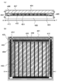
도 1은 발광 소자의 개념도.
도 2는 발광층의 에너지 이동을 도시하는 도면.
도 3은 조명 장치의 개념도.
도 4는 패시브 매트릭스형 발광 장치의 개념도.
도 5는 액티브 매트릭스형 발광 장치의 개념도.
도 6은 액티브 매트릭스형 발광 장치의 개념도.
도 7은 전자 기기를 도시하는 도면.
도 8은 조명 장치를 도시하는 도면.
도 9는 차량 탑재 표시 장치 및 전자 기기를 도시하는 도면.
도 10은 여기 착체의 발광 파장에 대하여 설명하는 도면.
도 11은 실시예 1의 발광 소자 1 및 비교 발광 소자 1의 구성을 도시하는 도면.
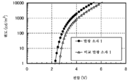
도 12는 실시예 1의 발광 소자 1 및 비교 발광 소자 1의 전압-휘도 특성을 도시하는 도면.
도 13은 실시예 1의 발광 소자 1 및 비교 발광 소자 1의 휘도-전류 효율 특성을 도시하는 도면.
도 14는 실시예 1의 발광 소자 1 및 비교 발광 소자 1의 휘도-전력 효율 특성을 도시하는 도면.
도 15는 실시예 1의 발광 소자 1 및 비교 발광 소자 1의 휘도-외부 양자 효율을 도시하는 도면.
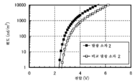
도 16은 실시예 2의 발광 소자 2 및 비교 발광 소자 2의 전압-휘도 특성을 도시하는 도면.
도 17은 실시예 2의 발광 소자 2 및 비교 발광 소자 2의 휘도-전류 효율 특성을 도시하는 도면.
도 18은 실시예 2의 발광 소자 2 및 비교 발광 소자 2의 전압-전류 특성을 도시하는 도면.
도 19는 실시예 2의 발광 소자 2 및 비교 발광 소자 2의 휘도-전력 효율 특성을 도시하는 도면.
도 20은 실시예 2의 발광 소자 2 및 비교 발광 소자 2의 휘도-외부 양자 효율 특성을 도시하는 도면.
도 21은 실시예 2의 발광 소자 2 및 비교 발광 소자 2의 발광 스펙트럼을 도시하는 도면.
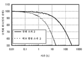
도 22는 실시예 2의 발광 소자 2 및 비교 발광 소자 2의 신뢰성 시험의 결과를 도시하는 도면.
도 23은 실시예 3의 발광 소자 3 및 비교 발광 소자 3의 전압-휘도 특성을 도시하는 도면.
도 24는 실시예 3의 발광 소자 3 및 비교 발광 소자 3의 휘도-전류 효율 특성을 도시하는 도면.
도 25는 실시예 3의 발광 소자 3 및 비교 발광 소자 3의 전압-전류 특성을 도시하는 도면.
도 26은 실시예 3의 발광 소자 3 및 비교 발광 소자 3의 휘도-전력 효율 특성을 도시하는 도면.
도 27은 실시예 3의 발광 소자 3 및 비교 발광 소자 3의 휘도-외부 양자 효율 특성을 도시하는 도면.
도 28은 실시예 3의 발광 소자 3 및 비교 발광 소자 3의 발광 스펙트럼을 도시하는 도면.
도 29는 실시예 3의 발광 소자 3 및 비교 발광 소자 3의 신뢰성 시험의 결과를 도시하는 도면.
도 30은 실시예 4의 발광 소자 4 및 비교 발광 소자 4의 전압-휘도 특성을 도시하는 도면.
도 31은 실시예 4의 발광 소자 4 및 비교 발광 소자 4의 휘도-전류 효율 특성을 도시하는 도면.
도 32는 실시예 4의 발광 소자 4 및 비교 발광 소자 4의 전압-전류 특성을 도시하는 도면.
도 33은 실시예 4의 발광 소자 4 및 비교 발광 소자 4의 휘도-전력 효율 특성을 도시하는 도면.
도 34는 실시예 4의 발광 소자 4 및 비교 발광 소자 4의 휘도-외부 양자 효율 특성을 도시하는 도면.
도 35는 실시예 4의 발광 소자 4 및 비교 발광 소자 4의 발광 스펙트럼을 도시하는 도면.
도 36은 실시예 4의 발광 소자 4 및 비교 발광 소자 4의 신뢰성 시험의 결과를 도시하는 도면.1 is a conceptual view of a light emitting device;
2 is a diagram showing energy transfer in a light emitting layer;
3 is a conceptual view of a lighting device.
4 is a conceptual view of a passive matrix type light emitting device.
5 is a conceptual view of an active matrix light emitting device.
6 is a conceptual diagram of an active matrix type light emitting device.
7 is a view showing an electronic apparatus;
8 is a view showing a lighting device.
9 is a view showing an in-vehicle display apparatus and an electronic apparatus.
10 is a view for explaining emission wavelength of an excited complex;
11 is a view showing the constructions of the light-emitting
12 is a diagram showing voltage-luminance characteristics of the light-emitting
13 is a graph showing the luminance-current efficiency characteristics of the light-emitting
14 is a graph showing the luminance-power efficiency characteristics of the light-emitting
15 is a graph showing the luminance-external quantum efficiency of the light-emitting
16 is a diagram showing voltage-luminance characteristics of the light-emitting
17 is a diagram showing luminance-current efficiency characteristics of the light-emitting
18 is a diagram showing voltage-current characteristics of the light-emitting
19 is a graph showing the luminance-power efficiency characteristics of the light-emitting
20 is a diagram showing luminance-external quantum efficiency characteristics of the light-emitting
21 is a diagram showing the luminescence spectra of the light-emitting
22 is a diagram showing the results of a reliability test of the
23 is a diagram showing voltage-luminance characteristics of the light-emitting
24 is a graph showing the luminance-current efficiency characteristics of the light-emitting
25 is a graph showing voltage-current characteristics of the light-emitting
26 is a graph showing the luminance-power efficiency characteristics of the light-emitting
27 is a graph showing the luminance-external quantum efficiency characteristics of the light-emitting
28 is a diagram showing the emission spectra of the light-emitting
29 is a diagram showing the results of a reliability test of the
30 is a diagram showing voltage-luminance characteristics of the light-emitting
31 is a graph showing luminance-current efficiency characteristics of the light-emitting
32 is a diagram showing voltage-current characteristics of the light-emitting
33 is a graph showing luminance-power efficiency characteristics of the light-emitting
34 is a graph showing the luminance-external quantum efficiency characteristics of the light-emitting
35 is a diagram showing the luminescence spectra of the light-emitting
36 is a diagram showing the results of a reliability test of the light-emitting
이하, 본 발명의 실시의 형태에 대하여 도면을 사용하여 상세하게 설명한다. 단, 본 발명은 이하의 설명에 한정되지 않고, 본 발명의 취지 및 그 범위로부터 일탈하지 않고 그 형태 및 상세를 다양하게 변경할 수 있는 것은 당업자라면 용이하게 이해된다. 따라서, 본 발명은 이하에 기재하는 실시 형태의 기재 내용에 한정하여 해석되는 것은 아니다.Hereinafter, embodiments of the present invention will be described in detail with reference to the drawings. However, the present invention is not limited to the following description, and it is easily understood by those skilled in the art that various changes in form and detail can be made without departing from the spirit and scope of the present invention. Accordingly, the present invention is not construed as being limited to the description of the embodiments described below.
(실시 형태 1) (Embodiment 1)
열 활성화 지연 형광체와, 형광을 발하는 재료를 혼합하여 사용한 발광 소자에서는, 이하와 같은 에너지의 과정을 거쳐 발광이 일어난다.In a light emitting device using a mixture of a thermal activation retardation fluorescent material and a fluorescent material, light emission occurs through the following energy process.
(1) 전자 및 정공(홀)이 형광을 발하는 재료에 있어서 재결합하여, 형광을 발하는 재료가 여기 상태로 되는 경우(직접 재결합 과정).(1) When electrons and holes (holes) are recombined in a material emitting fluorescence, and a material emitting fluorescence is brought into an excited state (direct recombination process).
(1-1) 형광을 발하는 재료의 여기 상태가 일중항 여기 상태일 때. : 형광을 발한다.(1-1) When the excited state of the material emitting fluorescence is singlet excited state. : It emits fluorescence.
(1-2) 형광을 발하는 재료의 여기 상태가 삼중항 여기 상태일 때. : 열 실활한다.(1-2) When the excited state of the fluorescent material is triplet excited state. : Heat is inactive.
상기 (1)의 직접 재결합 과정에 있어서는, 형광 양자 효율이 높으면, 높은 발광 효율이 얻어진다. 또한, 열 활성화 지연 형광체의 일중항 여기 상태의 준위는 형광을 발하는 재료의 일중항 여기 상태의 준위보다도 높은 것이 바람직하다.In the direct recombination process of (1) above, high fluorescence quantum efficiency results in high luminescence efficiency. It is preferable that the singlet excitation state level of the thermal activation retardation phosphor is higher than the singlet excitation state level of the material emitting fluorescence.
(2) 전자 및 정공(홀)이 열 활성화 지연 형광체에 있어서 재결합하여, 열 활성화 지연 형광체가 여기 상태로 되는 경우(에너지 이동 과정).(2) In the case where electrons and holes (holes) recombine in the thermally-activating retarded fluorescent material and the thermal activation retarded fluorescent material is brought into an excited state (energy transfer process).
(2-1) 열 활성화 지연 형광체의 여기 상태가 일중항 여기 상태일 때(2-1) When the excitation state of the thermal activation retardation phosphor is singlet excited state
열 활성화 지연 형광체의 일중항 여기 상태의 준위가, 형광을 발하는 재료의 일중항 여기 상태의 준위보다도 높은 경우, 열 활성화 지연 형광체로부터, 형광을 발하는 재료로 여기 에너지가 이동하여, 형광을 발하는 재료가 일중항 여기 상태로 된다. 일중항 여기 상태로 된 형광을 발하는 재료는 형광을 발한다. 또한, 열 활성화 지연 형광체의 일중항 여기 상태의 준위로부터, 형광을 발하는 재료의 삼중항 여기 상태의 준위로의 에너지 이동은, 형광을 발하는 재료에 있어서의 일중항 기저 상태로부터 삼중항 여기 상태로의 직접 전이가 금제인 점에서, 주된 에너지 이동 과정으로 되기 어렵기 때문에, 여기에서는 생략한다. 즉, 하기 수학식 (2-1)과 같이, 열 활성화 지연 형광체의 일중항 여기 상태(1H*)로부터, 형광을 발하는 재료의 일중항 여기 상태(1G*)로의 에너지 이동이 중요하다(수학식 중 1G는 형광을 발하는 재료의 일중항 기저 상태, 1H는 열 활성화 지연 형광체의 일중항 기저 상태를 나타낸다). When the level of the singly excited state of the thermally-activating retarder is higher than the level of the singly excited state of the material emitting the fluorescence, the excitation energy is shifted from the thermal activation retardation phosphor to the material emitting fluorescence, And becomes a singlet excited state. Fluorescent materials emit fluorescence in the singlet excited state. The energy transfer from the singlet excited state level of the thermally-activatable retarder to the triplet excited state level of the material emitting fluorescence is the same as the energy transfer from the singlet ground state to the triplet excited state Since the direct transition is prohibited, it is difficult to proceed with the main energy transfer process, so it is omitted here. That is, to be, it is important to the energy transfer from the singlet excited state (1 H *) of the heat activated delayed fluorescent material, a singlet material emitting fluorescence excited state (G 1 *) as shown in Equation (2-1) ( 1 G in the equation represents the singlet state basis state of the fluorescent material, and 1 H represents the singlet state state of the thermal activation retardation fluorescent substance).
![]()
![]()
(2-2) 열 활성화 지연 형광체의 여기 상태가 삼중항 여기 상태일 때(2-2) When the excitation state of the thermal activation retardation phosphor is triplet excited state
열 활성화 지연 형광체의 일중항 여기 상태의 준위가 형광을 발하는 재료의 일중항 여기 상태의 준위보다도 높은 경우, 하기의 과정을 거쳐 발광이 일어난다. 우선, 열 활성화 지연 형광체의 삼중항 여기 상태의 준위로부터 역항간 교차에 의해, 열 활성화 지연 형광체의 일중항 여기 상태의 준위로 여기 에너지가 이동한다. 그 후 열 활성화 지연 형광체의 일중항 여기 상태의 준위로부터 형광을 발하는 재료의 일중항 여기 상태의 준위로 여기 에너지가 이동하여, 형광을 발하는 재료가 일중항 여기 상태로 된다. 일중항 여기 상태로 된 형광을 발하는 재료는 형광을 발한다.When the level of singlet excitation state of the thermal activation retardation phosphor is higher than the level of singlet excited state of the material emitting fluorescence, light emission occurs through the following process. First, excited energy is transferred to the singly excited state of the thermally-activating retarder by crossing the inverse of the triplet excited state of the thermally-activating retarder. Thereafter, excitation energy moves from the singlet excited state level of the thermal activation retardation phosphor to the singlet excited state level of the material emitting fluorescence, and the material emitting fluorescence becomes singlet excited state. Fluorescent materials emit fluorescence in the singlet excited state.
즉, 하기 수학식 (2-2)와 같이, 열 활성화 지연 형광체의 삼중항 여기 상태(3H*)로부터 역항간 교차에 의해 열 활성화 지연 형광체의 일중항 여기 상태(1H*)가 생성되고, 그 후 형광을 발하는 재료의 일중항 여기 상태(1G*)로 에너지 이동한다.That is, as shown in the following formula (2-2), the singlet excited state ( 1 H * ) of the thermal activation retardation phosphor is generated by crossing the triplet excited state ( 3 H * ) of the thermal activation retarding phosphor , And then energy is transferred to the singlet excited state ( 1 G * ) of the fluorescent material.
![]()
![]()
상기 (2)에서 설명한 모든 에너지 이동 과정이 효율적으로 발생하면, 열 활성화 지연 형광체의 삼중항 여기 에너지 및 일중항 여기 에너지 모두 효율적으로 형광을 발하는 재료의 일중항 여기 상태(1G*)로 변환되기 때문에, 고효율의 발광이 가능해진다. 반대로, 열 활성화 지연 형광체로부터 형광을 발하는 재료로 여기 에너지가 이동하기 전에, 열 활성화 지연 형광체 자체가 그 여기 에너지를 광 또는 열로서 방출하여 실활해 버리면, 발광 효율이 저하되게 된다.When all of the energy transfer processes described in (2) above occur efficiently, both the triplet excitation energy and the singlet excitation energy of the thermal activation retardation phosphor are efficiently converted to the singlet excitation state ( 1 G * ) of the fluorescent material Thus, high-efficiency light emission is possible. On the contrary, if the thermal activation delayed fluorescent material itself emits the excited energy as light or heat and inactivates before the excitation energy moves from the thermal activation retarding fluorescent material to the fluorescent material, the light emitting efficiency is lowered.
이어서, 상술한 열 활성화 지연 형광체와 형광을 발하는 재료의 분자간의 에너지 이동 과정의 지배 인자에 대하여 설명한다. 분자간의 에너지 이동의 기구로서는, 포스터(Forster) 기구와 덱스터(Dexter) 기구의 2개의 기구가 제창되고 있다.Next, the dominant factors of the energy transfer process between the above-mentioned thermally activated retarder and the molecule of the fluorescent material will be described. As mechanisms of energy transfer between molecules, two mechanisms are proposed, namely a Forster mechanism and a Dexter mechanism.
우선, 첫번째 기구인 포스터 기구(쌍극자-쌍극자 상호 작용)는, 에너지 이동에, 분자간의 직접적 접촉을 필요로 하지 않고, 열 활성화 지연 형광체 및 형광을 발하는 재료간의 쌍극자 진동의 공명 현상을 통하여 에너지 이동이 일어나는 기구이다. 쌍극자 진동의 공명 현상에 의해 열 활성화 지연 형광체가 형광을 발하는 재료에 에너지를 주고 받아, 열 활성화 지연 형광체가 기저 상태로 되고, 형광을 발하는 재료가 여기 상태로 된다. 또한, 포스터 기구의 속도 상수 kh*→g를 수학식 (1)로 나타낸다.First, the poster mechanism (dipole-dipole interaction), which is the first mechanism, does not require direct contact between the molecules in energy transfer, but rather causes energy transfer through resonance of dipole oscillation between the thermally activated retarder and the fluorescent material It is an apparatus that arises. Due to the resonance phenomenon of the dipole oscillation, the thermal activation delayed fluorescent material imparts energy to the material emitting fluorescence, and the thermal activation delayed fluorescent material becomes a ground state, and the material emitting fluorescence becomes an excited state. Further, the velocity constant k h * - g of the poster mechanism is expressed by the equation (1).

수학식 (1)에 있어서, ν는 진동수를 나타내고, f'h(ν)는 열 활성화 지연 형광체의 규격화된 발광 스펙트럼(일중항 여기 상태로부터의 에너지 이동을 논하는 경우에는 형광 스펙트럼, 삼중항 여기 상태로부터의 에너지 이동을 논하는 경우에는 인광 스펙트럼)을 나타내고, εg(ν)는 형광을 발하는 재료의 몰 흡광 계수를 나타내고, N은 아보가드로수를 나타내고, n은 매체의 굴절률을 나타내고, R은 열 활성화 지연 형광체와 형광을 발하는 재료의 분자간 거리를 나타내고, τ는 실측되는 여기 상태의 수명(형광 수명이나 인광 수명)을 나타내고, φ는 발광 양자 수율(일중항 여기 상태로부터의 에너지 이동을 논하는 경우에는 형광 양자 수율, 삼중항 여기 상태로부터의 에너지 이동을 논하는 경우에는 인광 양자 수율)을 나타내고, K2는 열 활성화 지연 형광체와 형광을 발하는 재료의 전이 쌍극자 모멘트의 배향을 나타내는 계수(0 내지 4)이다. 또한, 랜덤 배향의 경우에는 K2=2/3이다.In the formula (1), v denotes a frequency, f ' h (v) denotes a normalized emission spectrum of the thermal activation retarding phosphor (fluorescence spectrum when discussing energy transfer from singlet excited state, (N) represents the refractive index of the medium, R represents the refractive index of the medium, and? G (?) Represents the molar extinction coefficient of the material that emits fluorescence, N represents Avogadro's number, Represents the lifetime (fluorescent lifetime or phosphorescence lifetime) of the actually observed excited state, and [phi] represents the emission quantum yield (energy transfer from singlet excited state) case, fluorescence quantum yield, if the non-energy transfer from a triplet excited state, represents a phosphorescence quantum yield), K 2 is a heat activated delayed fluorescence It is a coefficient that represents the orientation of the transition dipole moment of the material that emits fluorescence (0-4). In the case of random orientation, K 2 = 2/3.
이어서, 두번째 기구인 덱스터 기구(전자 교환 상호 작용)에서는, 열 활성화 지연 형광체와 형광을 발하는 재료가 궤도의 중첩을 발생시키는 접촉 유효 거리에 접근하고, 여기 상태의 열 활성화 지연 형광체의 전자와 기저 상태의 형광을 발하는 재료의 전자의 교환을 통하여 에너지 이동이 일어난다. 또한, 덱스터 기구의 속도 상수 kh*→g를 수학식 (2)로 나타낸다.Then, in the second mechanism, the dexter mechanism (electron exchange interaction), the thermal activation delayed fluorescent material and the fluorescent material approach the contact effective distance causing the overlap of the orbit, and the electrons of the excited thermal activation retarded fluorescent material and the base state Energy transfer occurs through the exchange of electrons in the fluorescent material. Further, the rate constant k h * - g of the Dexter mechanism is expressed by Equation (2).
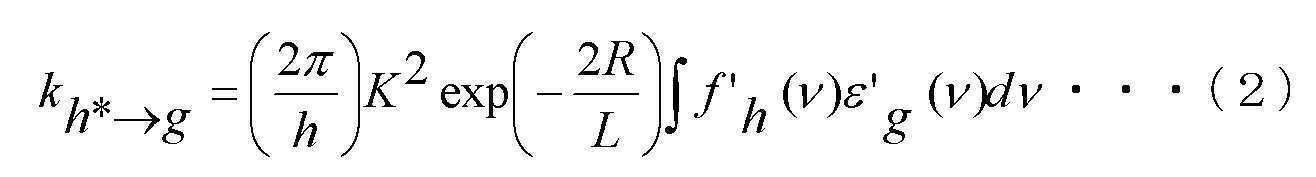
수학식 (2)에 있어서, h는 플랑크 상수이며, K는 에너지의 차원을 갖는 상수이며, ν는 진동수를 나타내고, f'h(ν)는 열 활성화 지연 형광체의 규격화된 발광 스펙트럼(일중항 여기 상태로부터의 에너지 이동을 논하는 경우에는 형광 스펙트럼, 삼중항 여기 상태로부터의 에너지 이동을 논하는 경우에는 인광 스펙트럼)을 나타내고, ε'g(ν)는 형광을 발하는 재료의 규격화된 흡수 스펙트럼을 나타내고, L은 실효 분자 반경을 나타내고, R은 열 활성화 지연 형광체와 형광을 발하는 재료의 분자간 거리를 나타낸다.In Equation (2), h is a Planck constant, K is a constant having a dimension of energy, v is a frequency, f ' h (v) is a normalized excitation spectrum of a thermal activation retarding phosphor Represents a fluorescence spectrum when discussing energy transfer from a state, or a phosphorescence spectrum when discussing energy transfer from a triplet excited state), 竜 ' g (僚) represents a normalized absorption spectrum of a material emitting fluorescence , L represents the effective molecular radius, and R represents the intermolecular distance of the material which emits fluorescence with the thermal activation retarding phosphor.
여기서, 열 활성화 지연 형광체로부터 형광을 발하는 재료로의 에너지 이동 효율 ΦET는, 수학식 (3)으로 나타난다고 생각되어진다. kr은 열 활성화 지연 형광체의 발광 과정(일중항 여기 상태로부터의 에너지 이동을 논하는 경우에는 형광, 삼중항 여기 상태로부터의 에너지 이동을 논하는 경우에는 인광)의 속도 상수를 나타내고, kn은 열 활성화 지연 형광체의 비발광 과정(열 실활이나 항간 교차)의 속도 상수를 나타내고, τ는 실측되는 열 활성화 지연 형광체의 여기 상태의 수명을 나타낸다.Here, it is considered that the energy transfer efficiency Φ ET from the thermal activation retarding phosphor to the material emitting fluorescence is represented by the following equation (3). k r is the rate constant of the thermal activation retarding phosphor (fluorescence when discussing energy transfer from singlet excited state, phosphorescence when discussing energy transfer from triplet excited state), k n Represents the rate constant of the non-emission process (thermal deactivation or intersection crossing) of the thermally activated retarded phosphor, and τ represents the lifetime of the excited state of the thermally activated retarded phosphor actually observed.

수학식 (3)으로부터, 에너지 이동 효율 ΦET를 높이기 위해서는, 에너지 이동의 속도 상수 kh*→g를 크게 하고, 다른 경합하는 속도 상수 kr+kn(=1/τ)이 상대적으로 작아지면 되는 것을 알 수 있다.From Equation (3), it is necessary to increase the energy transfer rate constant k h * → g and to increase the energy transfer efficiency Φ ET so that the other competitive rate constant k r + k n (= 1 / τ) is relatively small It can be seen that it is put down.
상기 (2-1) 및 (2-2)의 에너지 이동 과정의 어떤 경우든, 열 활성화 지연 형광체의 일중항 여기 상태(1H*)로부터 형광을 발하는 재료로의 에너지 이동이기 때문에, 포스터 기구(수학식 (1)) 및 덱스터 기구(수학식 (2)) 양쪽 기구에 의한 에너지 이동을 생각할 수 있다.In any of the energy transfer processes of (2-1) and (2-2), since the energy transfer from the singly excited state ( 1 H * ) of the thermal activation retardation phosphor to the material emitting fluorescence, Energy transfer by both mechanisms of equation (1)) and Dexter mechanism (equation (2)) can be considered.
우선, 포스터 기구에 의한 에너지 이동을 생각해 보자. 수학식 (1)과 수학식 (3)으로부터 τ를 소거하면, 에너지 이동 효율 ΦET는, 양자 수율 φ(일중항 여기 상태로부터의 에너지 이동을 논하고 있으므로, 형광 양자 효율)가 높은 편이 좋다고 할 수 있다. 그러나 실제로는, 더욱 중요한 팩터로서, 열 활성화 지연 형광체의 발광 스펙트럼(일중항 여기 상태로부터의 에너지 이동을 논하고 있으므로 형광 스펙트럼)과 형광을 발하는 재료의 흡수 스펙트럼(일중항 기저 상태로부터 일중항 여기 상태로의 전이에 상당하는 흡수)의 중첩이 큰 것도 필요하다(또한, 형광을 발하는 재료의 몰 흡광 계수도 높은 편이 바람직하다). 이것은, 열 활성화 지연 형광체의 발광 스펙트럼과, 형광을 발하는 재료의 최장파장측에 나타나는 흡수대가 중첩되는 것을 의미한다.First, consider the energy transfer by the poster mechanism. From the equations (1) and (3), it can be said that the energy transfer efficiency Φ ET is preferably higher than the quantum yield Φ (fluorescence quantum efficiency since energy transfer from singlet excited state is discussed) have. In practice, however, as a more important factor, the emission spectrum of the thermally-activating retarder (fluorescence spectrum is discussed because of energy transfer from the singlet excited state) and the absorption spectrum of the fluorescent material (monomodal ground state to singlet excitation state (The absorption corresponding to the transition of the fluorescence) is also required to be large (the molar extinction coefficient of the fluorescent material is also preferably high). This means that the emission spectrum of the thermally-activating retarder and the absorption band appearing on the longest wavelength side of the fluorescent material overlap.
이어서, 덱스터 기구에 의한 에너지 이동을 생각해 보자. 수학식 (2)에 의하면, 속도 상수 kh*→g를 크게 하기 위해서는 열 활성화 지연 형광체의 발광 스펙트럼(일중항 여기 상태로부터의 에너지 이동을 논하고 있으므로 형광 스펙트럼)과 형광을 발하는 재료의 흡수 스펙트럼(일중항 기저 상태로부터 일중항 여기 상태로의 전이에 상당하는 흡수)의 중첩이 큰 편이 좋은 것을 알 수 있다.Next, consider the energy transfer by the Dexter mechanism. According to the equation (2), in order to increase the rate constant k h * → g , the emission spectrum of the thermally-activating retarded fluorescent material (fluorescence spectrum for energy transfer from singlet excited state) and the absorption spectrum of the fluorescent material The absorption corresponding to the transition from the singlet state ground state to the singlet excitation state).
이상으로부터, (2-1), (2-2)의 어느 과정에 있어서든, 에너지 이동 효율의 최적화는, 열 활성화 지연 형광체의 발광 스펙트럼과, 형광을 발하는 재료의 최장파장측에 나타나는 흡수대가 중첩됨으로써 실현된다.Thus, in any of the processes (2-1) and (2-2), the optimization of the energy transfer efficiency is based on the fact that the emission spectrum of the thermal activation retardation fluorescent substance and the absorption band appearing on the longest wavelength side of the fluorescent material overlap .
단, 발광 소자로서 발광 효율을 높이기 위해서는, 열 활성화 지연 형광체가 삼중항 여기 상태로부터 일중항 여기 상태를 생성할 뿐만 아니라, 형광을 발하는 재료의 형광 양자 수율이 높은 것이 중요하다.However, in order to increase the luminous efficiency as a light emitting element, it is important that not only the thermal activation retarding phosphor generates singlet excited state from the triplet excited state but also the fluorescent quantum yield of the material emitting fluorescence is high.
그러나, 삼중항 여기 상태로부터 일중항 여기 상태를 생성할 수 있으며, 또한 형광 양자 수율이 높은 재료의 설계는 대단히 곤란하다.However, the singlet excited state can be generated from the triplet excited state, and the design of a material having a high fluorescent quantum yield is extremely difficult.
또한, (2)의 에너지 이동 과정의 비율이 많고, (1)의 직접 재결합 과정의 비율이 적은 쪽이, (1-2)의 열 실활 과정을 감소시킬 수 있기 때문에 바람직하다. 따라서, 형광을 발하는 재료의 농도는 5wt% 이하가 바람직하고, 1wt% 이하가 보다 바람직하다.It is also preferable that the ratio of the energy transfer process of (2) is large and the ratio of the direct recombination process of (1) is small, since the thermal inactivation process of (1-2) can be reduced. Therefore, the concentration of the fluorescent material is preferably 5 wt% or less, more preferably 1 wt% or less.
따라서 본 발명의 일 형태는, 형광을 발하는 재료를 발광 물질로서 사용한 경우의, 열 활성화 지연 형광체의 삼중항 여기 상태로부터의 형광을 발하는 재료로의 에너지 이동 효율 및 형광을 발하는 재료의 일중항 여기 상태의 형광 양자 효율에 관한 문제점을 극복할 수 있는, 유용한 방법을 제공한다. 이하에, 그 구체적인 형태를 설명한다.Accordingly, an aspect of the present invention is to provide an energy transfer efficiency from a triplet excited state of a thermal activation retarding fluorescent material to a material that emits fluorescence and a singlet excitation state of a material that emits fluorescence when a fluorescent material is used as a light emitting material Lt; RTI ID = 0.0 > fluorescence < / RTI > efficiency. The specific form thereof will be described below.
본 발명의 일 형태에서는, 형광을 발하는 재료에 효율적으로 에너지 이동이 가능한 에너지 도너로서, 열 활성화 지연 형광체를 사용한 발광 소자를 제공한다. 열 활성화 지연 형광체는, 그 일중항 여기 상태와, 삼중항 여기 상태가 근접하고 있다는 특징을 갖는다. 그로 인해, 열 활성화 지연 형광체는 삼중항 여기 상태로부터 일중항 여기 상태로의 전이가 일어나기 쉽다. 또한 에너지 억셉터인 형광을 발하는 재료의 일중항 여기 상태의 흡수 중 최장파장측의 흡수대(일중항 기저 상태로부터 일중항 여기 상태로의 전이에 상당하는 흡수)에, 열 활성화 지연 형광체의 발광 스펙트럼을 중첩시킴으로써, 열 활성화 지연 형광체의 삼중항 여기 상태 및 일중항 여기 상태로부터 형광을 발하는 재료의 일중항 여기 상태로의 에너지 이동 효율을 높일 수 있다.According to an aspect of the present invention, there is provided a light emitting device using an energy-activating retarder as an energy donor capable of efficiently transferring energy to a fluorescent material. The thermally-activating retarded phosphor has a characteristic that the singly excited state and the triplet excited state are close to each other. As a result, the thermal activation delayed phosphor is liable to undergo transition from triplet excited state to singlet excited state. Further, the absorption spectrum of the thermal activation retardation fluorescent material is shown in the absorption band on the longest wavelength side (absorption corresponding to the transition from the singlet state basis state to the singlet excitation state) among the absorption in the singlet excitation state of the material emitting fluorescence as the energy acceptor It is possible to increase the energy transfer efficiency from the triplet excited state and the singlet excited state of the thermal activation retarding fluorescent material to the singlet excited state of the fluorescent material.
또한, 삼중항 여기 상태로부터 일중항 여기 상태를 생성하는 기능과, 일중항 여기 상태로부터 효율적으로 발광을 얻는 기능을 상이한 재료에 담당시킴으로써, 발광 물질로서 열 활성화 지연의 유무와 관계없이 형광 양자 수율이 높은 재료(예를 들어 형광 양자 수율이 50% 이상인 재료)를 선택할 수 있다.Further, by taking the function of generating a singlet excited state from the triplet excited state and the function of efficiently obtaining light emission from the singlet excited state as different materials, the fluorescence quantum yield A high material (for example, a material having a fluorescence quantum yield of 50% or more) can be selected.
이에 의해, 열 활성화 지연 형광체의 삼중항 여기 상태 및 일중항 여기 상태의 에너지를, 형광을 발하는 재료의 일중항 여기 상태를 거쳐서 보다 효율적으로 발광으로 변환할 수 있어, 발광 효율이 높은 발광 소자로 하는 것이 가능해진다.As a result, the energy of the triplet excited state and singlet excited state of the thermal activation retardation phosphor can be more efficiently converted into light emission through the singlet excitation state of the material emitting fluorescence, Lt; / RTI >
이상과 같은 구성을 갖는 발광 소자는, 도 2와 같이 효율적으로 에너지 이동이 일어난다. 도 2에 있어서는, 전극(101)과 전극(102) 사이에 발광층(113)이 형성되어 있는 모습이 기재되어 있다. 각 전극과 발광층(113) 사이에는 임의의 층이 존재하고 있어도 좋다. 열 활성화 지연 형광체(113D)의 일중항 여기 상태 SD로부터는, 발광 물질(113A)의 일중항 여기 상태 SA로 에너지 이동이 일어난다. 또한, 열 활성화 지연 형광체(113D)의 삼중항 여기 상태 TD는, 열 활성화 지연 형광체(113D)의 일중항 여기 상태 SD로 역항간 교차하고 나서, 발광 물질(113A)의 일중항 여기 상태 SA로 에너지 이동이 일어난다. 그리고 발광 물질(113A)의 일중항 여기 상태 SA로부터 발광이 일어난다. 이렇게 본 실시 형태에 있어서의 발광 소자에서는, 삼중항 여기 상태로부터 일중항 여기 상태를 생성하는 기능과, 일중항 여기 상태로부터 효율적으로 발광을 얻는 기능을 상이한 재료에 담당시킴으로써, 에너지 이동 및 발광이 각각 양호하게 행해져, 발광 효율이 높은 발광 소자를 제공할 수 있다.In the light emitting device having the above-described structure, energy transfer occurs efficiently as shown in FIG. In Fig. 2, a state in which the
도 1에 본 실시 형태에 있어서의 발광 소자의 개념도를 도시한다. 도 1의 (A)는 발광 소자의 도면, 도 1의 (B) 및 도 1의 (C)는 발광층(113)만을 확대하여 도시한 도면이다.Fig. 1 is a conceptual diagram of a light emitting element in the present embodiment. 1 (A) is a view of a light emitting device, and FIG. 1 (B) and FIG. 1 (C) are enlarged views of only a
발광 소자는 제1 전극(101) 및 제2 전극(102)의 한 쌍의 전극에 끼워진 EL층(103)을 갖고 있으며, EL층(103)은 유기 화합물을 발광 물질로서 포함한다. 또한, EL층은 발광층(113)을 갖고 있으며, 발광 물질은 적어도 발광층(113)에 포함된다. 발광층(113) 이외의 층에 대해서는, 한정되지 않기 때문에, 그 밖의 층은 어떤 층을 사용해도 좋지만, 대표적인 적층 구조로서는, 정공 주입층(111), 정공 수송층(112), 전자 수송층(114), 전자 주입층(115) 등이 있다. 이 외에, 캐리어 블록층 등을 형성해도 좋고, 발광층을 복수 형성해도 좋다.The light emitting element has an
발광층(113)에는 열 활성화 지연 형광체(113D) 및 발광 물질(113A)이 포함되어 있다. 도 1의 (B)에 도시한 바와 같이, 열 활성화 지연 형광체(113D)는 단독으로 삼중항 여기 상태로부터 역항간 교차에 의해 일중항 여기 상태를 생성할 수 있는 재료로 구성되어도 좋다. 또한 열 활성화 지연 형광체(113D)는 복수종의 재료로 구성되어 있어도 좋다. 그 중에서도 도 1의 (C)에 도시한 바와 같이, 제1 유기 화합물(113D1) 및 제2 유기 화합물(113D2)의 2종의 재료로 구성되며, 이들이 여기 착체(엑시플렉스)를 형성하는 조합이면 특히 바람직하다. 엑시플렉스는 일중항 여기 상태의 준위와 삼중항 여기 상태의 준위의 차가 매우 작아지기 쉬운 성질을 갖고 있기 때문에, 삼중항 여기 상태의 준위로부터 일중항 여기 상태의 준위로의 에너지 이동이 일어나기 쉽다. 그 때문에 여기 착체를 형성하는 제1 유기 화합물과 제2 유기 화합물을 조합하여 구성된 열 활성화 지연 형광체는, 본 발명의 일 형태에 있어서의 열 활성화 지연 형광체로서 최적이다. 또한, 제1 유기 화합물과 제2 유기 화합물 중, 한쪽을 정공 수송성, 다른쪽을 전자 수송성의 재료로 하면, 제1 유기 화합물과 제2 유기 화합물의 혼합 비율을 조절함으로써, 발광층에 있어서의 정공과 전자의 캐리어 밸런스를 최적화하는 것이 용이하기 때문에, 발광 효율뿐만 아니라 신뢰성의 관점에서도 바람직하다. 또한, 본 실시 형태의 발광 소자에서는, 발광층(113)에 그 밖의 물질이 포함되어 있는 것을 배제하지 않는다.The
열 활성화 지연 형광체는 그 일중항 여기 상태와 삼중항 여기 상태가 근접하고 있는 상태에 있지만, 특히 일중항 여기 상태와 삼중항 여기 상태의 에너지 차가 0eV 이상 0.2eV 이하인 것이 바람직하다.The thermal activation retardation phosphor is in a state in which the singly excited state and the triplet excited state are in close proximity to each other. In particular, the energy difference between the singly excited state and the triplet excited state is preferably 0 eV or more and 0.2 eV or less.
또한, 이 열 활성화 지연 형광체와 형광을 발하는 재료는, 상술한 바와 같이 열 활성화 지연 형광체의 발광과, 발광 물질(113A)의 최장파장측의 흡수대가 중첩되는 조합인 것이 바람직하다. 이것에 의해, 열 활성화 지연 형광체의 일중항 여기 상태로부터 형광을 발하는 재료의 일중항 여기 상태로 효율적으로 에너지의 이동이 행해진다.It is preferable that the material for emitting the thermal activation retarding fluorescent substance and the fluorescent material is a combination in which the light emission of the thermal activation retardation fluorescent substance and the absorption band on the longest wavelength side of the
상기 발광 물질(113A)로서 사용할 수 있는 형광을 발하는 재료로서는 예를 들어, 이하와 같은 것을 들 수 있다. 5,6-비스[4-(10-페닐-9-안트릴)페닐]-2,2'-비피리딘(약칭: PAP2BPy), 5,6-비스[4'-(10-페닐-9-안트릴)비페닐-4-일]-2,2'-비피리딘(약칭: PAPP2BPy), N,N'-비스〔4-(9-페닐-9H-플루오렌-9-일)페닐〕-N,N'-디페닐-피렌-1,6-디아민(약칭: 1,6FLPAPrn), N,N'-비스[4-(9H-카르바졸-9-일)페닐]-N,N'-디페닐스틸벤-4,4'-디아민(약칭: YGA2S), 4-(9H-카르바졸-9-일)-4'-(10-페닐-9-안트릴)트리페닐아민(약칭: YGAPA), 4-(9H-카르바졸-9-일)-4'-(9,10-디페닐-2-안트릴)트리페닐아민(약칭: 2YGAPPA), N,9-디페닐-N-[4-(10-페닐-9-안트릴)페닐]-9H-카르바졸-3-아민(약칭: PCAPA), 페릴렌, 2,5,8,11-테트라-tert-부틸페릴렌(약칭: TBP), 4-(10-페닐-9-안트릴)-4'-(9-페닐-9H-카르바졸-3-일)트리페닐아민(약칭: PCBAPA), N,N"-(2-tert-부틸안트라센-9,10-디일디-4,1-페닐렌)비스[N,N',N'-트리페닐-1,4-페닐렌디아민](약칭: DPABPA), N,9-디페닐-N-[4-(9,10-디페닐-2-안트릴)페닐]-9H-카르바졸-3-아민(약칭: 2PCAPPA), N-[4-(9,10-디페닐-2-안트릴)페닐]-N,N',N'-트리페닐-1,4-페닐렌디아민(약칭: 2DPAPPA), N,N,N',N',N",N",N''',N'''-옥타페닐디벤조[g,p]크리센-2,7,10,15-테트라아민(약칭: DBC1), 쿠마린 30, N-(9,10-디페닐-2-안트릴)-N,9-디페닐-9H-카르바졸-3-아민(약칭: 2PCAPA), N-[9,10-비스(1,1'-비페닐-2-일)-2-안트릴]-N,9-디페닐-9H-카르바졸-3-아민(약칭: 2PCABPhA), N-(9,10-디페닐-2-안트릴)-N,N',N'-트리페닐-1,4-페닐렌디아민(약칭: 2DPAPA), N-[9,10-비스(1,1'-비페닐-2-일)-2-안트릴]-N,N',N'-트리페닐-1,4-페닐렌디아민(약칭: 2DPABPhA), 9,10-비스(1,1'-비페닐-2-일)-N-[4-(9H-카르바졸-9-일)페닐]-N-페닐안트라센-2-아민(약칭: 2YGABPhA), N,N,9-트리페닐안트라센-9-아민(약칭: DPhAPhA)쿠마린 545T, N,N'-디페닐퀴나크리돈(약칭: DPQd), 루브렌, 5,12-비스(1,1'-비페닐-4-일)-6,11-디페닐테트라센(약칭: BPT), 2-(2-{2-[4-(디메틸아미노)페닐]에테닐}-6-메틸-4H-피란-4-일리덴)프로판디니트릴(약칭: DCM1), 2-{2-메틸-6-[2-(2,3,6,7-테트라히드로-1H,5H-벤조[ij]퀴놀리진-9-일)에테닐]-4H-피란-4-일리덴}프로판디니트릴(약칭: DCM2), N,N,N',N'-테트라키스(4-메틸페닐)테트라센-5,11-디아민(약칭: p-mPhTD), 7,14-디페닐-N,N,N',N'-테트라키스(4-메틸페닐)아세나프토[1,2-a]플루오란텐-3,10-디아민(약칭: p-mPhAFD), 2-{2-이소프로필-6-[2-(1,1,7,7-테트라메틸-2,3,6,7-테트라히드로-1H,5H-벤조[ij]퀴놀리진-9-일)에테닐]-4H-피란-4-일리덴}프로판디니트릴(약칭: DCJTI), 2-{2-tert-부틸-6-[2-(1,1,7,7-테트라메틸-2,3,6,7-테트라히드로-1H, 5H-벤조[ij]퀴놀리진-9-일)에테닐]-4H-피란-4-일리덴}프로판디니트릴(약칭: DCJTB), 2-(2,6-비스{2-[4-(디메틸아미노)페닐]에테닐}-4H-피란-4-일리덴)프로판디니트릴(약칭: BisDCM), 2-{2,6-비스[2-(8-메톡시-1,1,7,7-테트라메틸-2,3,6,7-테트라히드로-1H,5H-벤조[ij]퀴놀리진-9-일)에테닐]-4H-피란-4-일리덴}프로판디니트릴(약칭: BisDCJTM) 등을 들 수 있다.Examples of the fluorescent material that can be used as the
상술한 형광을 발하는 재료의, 발광층(113) 중의 농도는 5wt% 이하가 바람직하고, 1wt% 이하가 보다 바람직하다. 이러한 농도로 함으로써, (2)의 에너지 이동 과정의 비율을 많게, (1)의 직접 재결합 과정의 비율을 적게 하여, (1-2)의 열 실활 과정을 감소시킬 수 있다.The concentration of the fluorescent material in the
열 활성화 지연 형광체로서는, 예를 들어 1종의 재료로 구성되는 경우에는 이하와 같은 것을 사용할 수 있다.As the thermal activation retardation phosphor, for example, the following thermal phosphor can be used when it is composed of one kind of material.
우선, 풀러렌이나 그의 유도체, 프로플라빈 등의 아크리딘 유도체, 에오신 등을 들 수 있다. 또한 마그네슘(Mg), 아연(Zn), 카드뮴(Cd), 주석(Sn), 백금(Pt), 인듐(In), 혹은 팔라듐(Pd) 등을 포함하는 금속 함유 포르피린을 들 수 있다. 상기 금속 함유 포르피린으로서는, 예를 들어 이하의 화학식으로 나타내는 프로토포르피린-불화주석 착체(SnF2(Proto IX)), 메소포르피린-불화주석 착체(SnF2(Meso IX)), 헤마토포르피린-불화주석 착체(SnF2(Hemato IX)), 코프로포르피린테트라메틸에스테르-불화주석 착체(SnF2(Copro III-4Me)), 옥타에틸포르피린-불화주석 착체(SnF2(OEP)), 에티오포르피린-불화주석 착체(SnF2(Etio I)), 옥타에틸포르피린-염화백금 착체(PtCl2OEP) 등도 들 수 있다.First, fullerene and its derivatives, acridine derivatives such as proparbene, and eosin are listed. And metal-containing porphyrins including magnesium (Mg), zinc (Zn), cadmium (Cd), tin (Sn), platinum (Pt), indium (In), or palladium (Pd). Examples of the metal-containing porphyrin include protoporphyrin-tin fluoride complexes (SnF 2 (Proto IX)), meso porphyrin-tin fluoride complex (SnF 2 (Meso IX)), hematoporphyrin- complex (SnF 2 (Hemato IX)) , the porphyrin tetramethyl ester as a Cope-fluoride tin complex (SnF 2 (Copro III-4Me )), octa-ethyl-porphyrin-fluoride tin complex (SnF 2 (OEP)), a thio porphyrin- Tin fluoride complex (SnF 2 (Etio I)), octaethylporphyrin-platinum chloride complex (PtCl 2 OEP), and the like.

또한, 1종의 재료로 구성되는 열 활성화 지연 형광체로서는, 이하의 화학식으로 나타내는 2-(비페닐-4-일)-4,6-비스(12-페닐린돌[2,3-a]카르바졸-11-일)-1,3,5-트리아진(PIC-TRZ) 등의 π 전자 과잉형 복소 방향환 및 π 전자 부족형 복소 방향환을 갖는 복소환 화합물도 사용할 수 있다. 상기 복소환 화합물은, π 전자 과잉형 복소 방향환 및 π 전자 부족형 복소 방향환을 갖기 때문에, 전자 수송성 및 정공 수송성이 높아, 바람직하다. 또한, π 전자 과잉형 복소 방향환과 π 전자 부족형 복소 방향환이 직접 결합한 물질은, π 전자 과잉형 복소 방향환의 도너성과 π 전자 부족형 복소 방향환의 억셉터성이 모두 강해져, 일중항 여기 상태의 준위와 삼중항 여기 상태의 준위의 차가 작아지기 때문에, 특히 바람직하다.Examples of the thermally-activating retarder composed of one kind of material include 2- (biphenyl-4-yl) -4,6-bis (12-phenylindol [2,3-a] -11-yl) -1,3,5-triazine (PIC-TRZ), etc., and heterocyclic compounds having a? -Electronic shortage complex aromatic ring can also be used. The heterocyclic compound is preferable because it has a? -Electron excess type heteroaromatic ring and a? -Electronic shortage type heteroaromatic ring and therefore has high electron transportability and hole transportability. Further, the substance in which the? -Electron excess type complex aromatic ring and the? -Electronic shortage type complex aromatic ring are directly bonded becomes stronger in both the donor state of the? -Electron excess complex ring and the acceptor of the? -Electron short type complex aromatic ring, And the difference in the level of the triplet excited state becomes smaller.

또한 열 활성화 지연 형광체로서, 제1 유기 화합물 및 제2 유기 화합물의, 2종의 여기 착체를 형성하는 조합의 유기 화합물을 사용할 수 있다. 이 경우 공지의 캐리어 수송 재료를 적절히 사용할 수 있지만, 효율적으로 여기 착체를 형성하기 위해, 전자를 수취하기 쉬운 화합물(전자 수송성을 갖는 재료)과, 정공을 수취하기 쉬운 화합물(정공 수송성을 갖는 재료)을 조합하는 것이 특히 바람직하다.Further, as the thermal activation retardation fluorescent substance, an organic compound of a combination of a first organic compound and a second organic compound to form two kinds of excited complexes can be used. In this case, a known carrier transporting material can be suitably used. However, in order to efficiently form an excited complex, a compound (a material having an electron transporting property) that easily receives electrons and a compound (a material having a hole transporting property) Is particularly preferable.
왜냐하면, 전자 수송성을 갖는 재료와, 정공 수송성을 갖는 재료를 조합하여 열 활성화 지연 형광체로서 사용하여, 전자 수송성을 갖는 재료 및 정공 수송성을 갖는 재료의 혼합 비율을 조절함으로써, 발광층에 있어서의 정공과 전자의 캐리어 밸런스를 최적화하는 것이 용이해지기 때문이다. 발광층에 있어서의 정공과 전자의 캐리어 밸런스를 최적화함으로써, 발광층 중에서 전자와 정공의 재결합이 일어나는 영역이 치우치는 것을 억제할 수 있다. 재결합이 일어나는 영역의 치우침을 억제함으로써, 발광 소자의 신뢰성을 향상시킬 수 있다.This is because, by combining a material having an electron transporting property and a material having a hole transporting property as a thermal activation retardation fluorescent material and controlling the mixing ratio of a material having an electron transporting property and a material having a hole transporting property, This is because it is easy to optimize the carrier balance. By optimizing the carrier balance of the holes and electrons in the light emitting layer, it is possible to suppress the shift of the regions where electron and hole recombination occur in the light emitting layer. The reliability of the light emitting device can be improved by suppressing the unevenness of the region where recombination occurs.
전자를 수취하기 쉬운 화합물(전자 수송성을 갖는 재료)로서는, π 전자 부족형 복소 방향족이나 금속 착체 등을 사용할 수 있다. 구체적으로는, 비스(10-히드록시벤조[h]퀴놀리나토)베릴륨(II)(약칭: BeBq2), 비스(2-메틸-8-퀴놀리놀라토)(4-페닐페놀라토)알루미늄(III)(약칭: BAlq), 비스(8-퀴놀리놀라토)아연(II)(약칭: Znq), 비스[2-(2-벤조옥사졸릴)페놀라토]아연(II)(약칭: ZnPBO), 비스[2-(2-벤조티아졸릴)페놀라토]아연(II)(약칭: ZnBTZ) 등의 금속 착체나, 2-(4-비페닐릴)-5-(4-tert-부틸페닐)-1,3,4-옥사디아졸(약칭: PBD), 3-(4-비페닐릴)-4-페닐-5-(4-tert-부틸페닐)-1,2,4-트리아졸(약칭: TAZ), 1,3-비스[5-(p-tert-부틸페닐)-1,3,4-옥사디아졸-2-일]벤젠(약칭: OXD-7), 9-[4-(5-페닐-1,3,4-옥사디아졸-2-일)페닐] -9H-카르바졸(약칭: CO11), 2,2',2"-(1,3,5-벤젠트리일)트리스(1-페닐-1H-벤즈이미다졸)(약칭: TPBI), 2-[3-(디벤조티오펜-4-일)페닐]-1-페닐-1H-벤즈이미다졸(약칭: mDBTBIm-II) 등의 폴리아졸 골격을 갖는 복소환 화합물이나, 2-[3-(디벤조티오펜-4-일)페닐]디벤조[f,h]퀴녹살린(약칭: 2mDBTPDBq-II), 2-[3'-(디벤조티오펜-4-일) 비페닐-3-일]디벤조[f,h]퀴녹살린(약칭: 2mDBTBPDBq-II), 2-[3'-(9H-카르바졸-9-일)비페닐-3-일]디벤조[f,h]퀴녹살린(약칭: 2mCzBPDBq), 4,6-비스[3-(페난트렌-9-일)페닐]피리미딘(약칭: 4,6mPnP2Pm), 4,6-비스3-(4-디벤조티에닐)페닐〕피리미딘(약칭: 4,6mDBTP2Pm-II) 등의 디아진 골격을 갖는 복소환 화합물이나, 3,5-비스[3-(9H-카르바졸-9-일)페닐]피리딘(약칭: 35DCzPPy), 1,3,5-트리[3-(3-피리딜)페닐]벤젠(약칭: TmPyPB) 등의 피리딘 골격을 갖는 복소환 화합물을 들 수 있다. 상술한 것 중에서도, 디아진 골격을 갖는 복소환 화합물이나 피리딘 골격을 갖는 복소환 화합물은, 신뢰성이 양호하여 바람직하다. 특히, 디아진(피리미딘이나 피라진) 골격을 갖는 복소환 화합물은, 전자 수송성이 높아, 구동 전압 저감에도 기여한다.As a compound (a material having an electron transporting property) that can easily receive electrons, a π electron shortage type heteroaromatic or metal complex can be used. Specific examples thereof include beryllium (II) (abbreviation: BeBq 2 ), bis (2-methyl-8-quinolinolato) (4-phenylphenolato) aluminum (II) (abbreviation: ZnPBO 3) (abbreviation: BAlq), bis (8-quinolinolato) zinc (II) (abbreviation: Znq), bis [2- (2-benzoxazolyl) phenolato] ), Bis [2- (2-benzothiazolyl) phenolato] zinc (II) (abbreviated as ZnBTZ), 2- (4-biphenylyl) -5- ) -1,3,4-oxadiazole (abbreviation: PBD), 3- (4-biphenylyl) -4-phenyl-5- (4- (Abbreviated as TAZ), 1,3-bis [5- (p-tert-butylphenyl) -1,3,4-oxadiazol- Phenyl] -9H-carbazole (abbreviated as CO11), 2,2 ', 2 "- (1,3,5-benzenetri 1-phenyl-1H-benzimidazole (abbreviation: TPBI), 2- [3- (dibenzothiophen-4-yl) phenyl] mDBTBIm-II) or a heterocyclic compound having a polyazole skeleton such as 2- [3- (dibenzo (Dibenzothiophen-4-yl) phenyl] dibenzo [f, h] quinoxaline (abbreviated as 2mDBTPDBq-II) Yl) dibenzo [f, h] quinoxaline (abbreviated as 2mDBTBPDBq-II), 2- [3'- (9H- (2mCzBPDBq), 4,6-bis [3- (phenanthren-9-yl) phenyl] pyrimidine (abbreviated as 4,6 mPnP2Pm), 4,6- 3- (9H-carbazol-9-yl) phenyl] pyridine (abbreviated as " 35DCzPPy "), 1 , And 3,5-tri [3- (3-pyridyl) phenyl] benzene (abbreviation: TmPyPB). Among the above, heterocyclic compounds having a diazine skeleton Or a heterocyclic compound having a pyridine skeleton are preferable because of good reliability. In particular, a heterocyclic compound having a diazine (pyrimidine or pyrazine) skeleton has high electron transportability and contributes to reduction of driving voltage.
정공을 수취하기 쉬운 화합물(정공 수송성을 갖는 재료)로서는, π 전자 과잉형 복소 방향족 또는 방향족 아민 등을 적절하게 사용할 수 있다. 구체적으로는, 2-[N-(9-페닐카르바졸-3-일)-N-페닐아미노]스피로-9,9'-비플루오렌(약칭: PCASF), 4,4'-비스[N-(1-나프틸)-N-페닐아미노]비페닐(약칭: NPB), N,N'-비스(3-메틸페닐)-N,N'-디페닐-[1,1'-비페닐]-4,4'-디아민(약칭: TPD), 4,4'-비스[N-(스피로-9,9'-비플루오렌-2-일)-N-페닐아미노]비페닐(약칭: BSPB), 4-페닐-4'-(9-페닐플루오렌-9-일)트리페닐아민(약칭: BPAFLP), 4-페닐-3'-(9-페닐플루오렌-9-일)트리페닐아민(약칭: mBPAFLP), 4-페닐-4'-(9-페닐-9H-카르바졸-3-일)트리페닐아민(약칭: PCBA1BP), 4,4'-디페닐-4"-(9-페닐-9H-카르바졸-3-일)트리페닐아민(약칭: PCBBi1BP), 4-(1-나프틸)-4'-(9-페닐-9H-카르바졸-3-일)트리페닐아민(약칭: PCBANB), 4,4'-디(1-나프틸)-4"-(9-페닐-9H-카르바졸-3-일)트리페닐아민(약칭: PCBNBB), 9,9-디메틸-N-페닐-N-[4-(9-페닐-9H-카르바졸-3-일)페닐]-플루오렌-2-아민(약칭: PCBAF), N-페닐-N-[4-(9-페닐-9H-카르바졸-3-일)페닐]-스피로-9,9'-비플루오렌-2-아민(약칭: PCBASF) 등의 방향족 아민 골격을 갖는 화합물이나, 1,3-비스(N-카르바졸릴)벤젠(약칭: mCP), 4,4'-디(N-카르바졸릴)비페닐(약칭: CBP), 3,6-비스(3,5-디페닐페닐)-9-페닐카르바졸(약칭: CzTP), 9-페닐-9H-3-(9-페닐-9H-카르바졸-3-일)카르바졸(약칭: PCCP) 등의 카르바졸 골격을 갖는 화합물이나, 4,4',4"-(벤젠-1,3,5-트리일)트리(디벤조티오펜)(약칭: DBT3P-II), 2,8-디페닐-4-[4-(9-페닐-9H-플루오렌-9-일)페닐]디벤조티오펜(약칭: DBTFLP-III), 4-[4-(9-페닐-9H-플루오렌-9-일)페닐]-6-페닐디벤조티오펜(약칭: DBTFLP-IV) 등의 티오펜 골격을 갖는 화합물이나, 4,4',4"-(벤젠-1,3,5-트리일)트리(디벤조푸란)(약칭: DBF3P-II), 4-{3-[3-(9-페닐-9H-플루오렌-9-일)페닐]페닐}디벤조푸란(약칭: mmDBFFLBi-II) 등의 푸란 골격을 갖는 화합물을 들 수 있다. 상술한 것 중에서도, 방향족 아민 골격을 갖는 화합물이나 카르바졸 골격을 갖는 화합물은, 신뢰성이 양호하고, 또한, 정공 수송성이 높아, 구동 전압 저감에도 기여하기 때문에 바람직하다.As a compound (a material having hole transportability) that can easily receive holes, a? -Electron excess type heteroaromatic or aromatic amine can be suitably used. Specific examples thereof include 2- [N- (9-phenylcarbazol-3-yl) -N-phenylamino] spiro-9,9'-bipluorene (abbreviation: PCASF), 4,4'-bis [N (NPB), N, N'-bis (3-methylphenyl) -N, N'-diphenyl- [1,1'-biphenyl] 4,4'-diamine (abbreviated as TPD), 4,4'-bis [N- (spiro-9,9'-bifluoren-2-yl) ), 4-phenyl-4 '- (9-phenylfluorene-9-yl) triphenylamine (abbreviation: BPAFLP) (Abbreviated as mBPAFLP), 4-phenyl-4 '- (9-phenyl-9H-carbazol-3-yl) triphenylamine (abbreviation: PCBA1BP), 4,4'- Phenyl-9H-carbazol-3-yl) triphenylamine (abbreviation: PCBBi1BP), 4- (1-naphthyl) -4 ' PCBANB), 4,4'-di (1-naphthyl) -4 "- (9-phenyl-9H-carbazol-3- yl) triphenylamine (abbreviation: PCBNBB), 9,9- N-phenyl-N- [4- (9-phenyl-9H-carbazol-3-yl) phenyl] 3-yl) phenyl] -spiro-9,9'-bifluorene-2-amine (abbreviation: PCBASF), or a compound having an aromatic amine skeleton such as 1,3-bis -Carbazolyl) benzene (abbreviated as mCP), 4,4'-di (N-carbazolyl) biphenyl (abbreviated as CBP), 3,6-bis (3,5- A compound having a carbazole skeleton such as phenylcarbazole (abbreviated as CzTP), 9-phenyl-9H-3- (9-phenyl-9H-carbazol- (Dibenzothiophene) (abbreviation: DBT3P-II), 2,8-diphenyl-4- [4- (9- 9-yl) phenyl] -6-phenyldibenzothiophene (abbrev., DBTFLP-III), 4- [4- (9- (Benzene-1,3,5-triyl) tri (dibenzofuran) (abbreviation: DBF3P-IV) (Abbreviation: " mmDBFFLBi-II "), and a compound having a furan skeleton such as 4- {3- [3- (9- phenyl-9H- fluoren- . Among the above-mentioned compounds, a compound having an aromatic amine skeleton and a compound having a carbazole skeleton are preferable because they have good reliability, high hole transportability, and contribute to a reduction in driving voltage.
제1 유기 화합물 및 제2 유기 화합물은, 이들에 한정되지 않고, 캐리어를 수송할 수 있고, 또한 여기 착체를 형성할 수 있는 조합이며, 상기 여기 착체의 발광이, 발광 물질의 흡수 스펙트럼에 있어서의 최장파장측의 흡수대(발광 물질의 일중항 기저 상태로부터 일중항 여기 상태로의 전이에 상당하는 흡수)와 중첩되어 있으면 되며, 공지의 다른 재료를 사용해도 좋다.The first organic compound and the second organic compound are not limited to these, but are combinations that can transport carriers and can form excited complexes, and the luminescence of the excited complexes is the absorption spectrum of the luminescent material It may be superimposed on the absorption band on the longest wavelength side (absorption corresponding to the transition of the light emitting material from the singlet excited state to the singlet excited state), or other known materials may be used.
또한, 전자 수송성을 갖는 재료와 정공 수송성을 갖는 재료에 의해 제1 유기 화합물 및 제2 유기 화합물을 구성하는 경우, 그 혼합비에 의해 캐리어 밸런스를 제어할 수 있다. 구체적으로는, 제1 유기 화합물:제2 유기 화합물=1:9 내지 9:1의 범위가 바람직하다.When the first organic compound and the second organic compound are constituted by a material having an electron transporting property and a material having a hole transporting property, the carrier balance can be controlled by the mixing ratio. Concretely, the ratio of the first organic compound: the second organic compound = 1: 9 to 9: 1 is preferable.
여기서, 여기 착체를 형성하는 각 화합물(제1 유기 화합물(113D1) 및 제2 유기 화합물(113D2)) 및 여기 착체에 대하여 조금 상세하게 설명한다.Here, the compounds (the first organic compound 113D1 and the second organic compound 113D2) forming the excitation complex and the excited complexes will be described in detail.
도 10의 (A), 도 10의 (B)에 4종의 유기 화합물 단독의 발광 스펙트럼과, 이들로 형성된 여기 착체의 발광 스펙트럼을 도시했다. 또한, 도면 중, 화합물 1이 2-[4-(디벤조티오펜-4-일)페닐]-1-페닐-1H-벤즈이미다졸(약칭: DBTBIm-II), 화합물 2가 2-[3-(디벤조티오펜-4-일)페닐]디벤조[f,h]퀴녹살린(약칭: 2mDBTPDBq-II), 화합물 3이 4,4',4"-트리스[N-(1-나프틸)-N-페닐아미노]트리페닐아민(약칭: 1'-TNATA), 화합물 4가 2,7-비스[N-(4-디페닐아미노페닐)-N-페닐아미노]-스피로-9,9'-비플루오렌(약칭: DPA2SF)이다. 여기 착체 1은 화합물 1과 화합물 3의 여기 착체, 여기 착체 2는 화합물 2와 화합물 3의 여기 착체, 여기 착체 3이 화합물 2와 4,4'-비스[N-(1-나프틸)-N-페닐아미노]비페닐(약칭: NPB)의 여기 착체, 여기 착체 4가 화합물 2와 화합물 4의 여기 착체의 스펙트럼이다.Fig. 10 (A) and Fig. 10 (B) show emission spectra of four types of organic compounds alone and emission spectra of excited complexes formed from these. In the figure, the
이하에 각 화합물의 화학식을 나타낸다.The chemical formula of each compound is shown below.
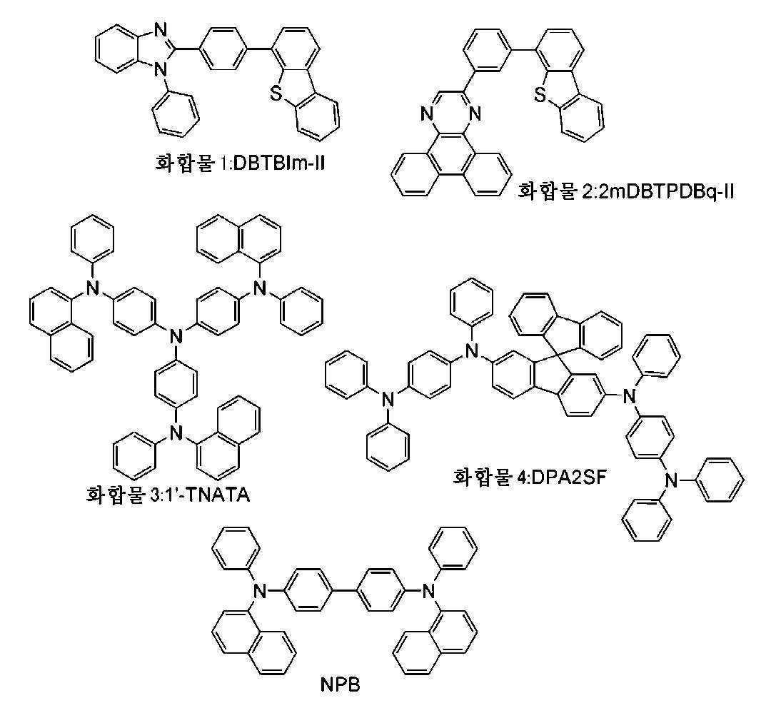
도 10의 (A)에는 여기 착체 1 및 여기 착체 2 외에, 화합물 1 내지 화합물 3의 발광 스펙트럼을 도시한다. 여기 착체 1로 표현되는 스펙트럼에는 화합물 1을 베이스로 화합물 3을 소량 첨가한 재료의 발광을 측정한 결과를, 여기 착체 2로 표현되는 스펙트럼에는, 화합물 2를 베이스로 화합물 3을 소량 첨가한 재료의 발광을 측정한 결과를 각각 나타냈다. 즉, 여기 착체 1의 측정을 행한 시료에 있어서는, 화합물 1과 화합물 3의 어느 한쪽이 제1 유기 화합물(113D1)에 상당하고, 다른쪽이 제2 유기 화합물(113D2)에 상당한다. 또한, 여기 착체 2의 측정을 행한 시료에 있어서는, 화합물 2와 화합물 3의 어느 한쪽이 제1 유기 화합물(113D1)에 상당하고, 다른쪽이 제2 유기 화합물(113D2)에 상당한다.FIG. 10 (A) shows the luminescence spectra of the
도 10의 (A)로부터 알 수 있는 바와 같이, 소량 성분인 화합물 3이 동일해도, 여기 착체 1과 여기 착체 2의 발광은 100nm 이상의 차가 있다. 즉, 베이스의 물질을 변경함으로써, 여기 착체의 발광 파장을 용이하게 조정할 수 있다.As can be seen from Fig. 10 (A), even if
또한, 여기 착체 1의 발광 스펙트럼의 피크 파장은 520nm 정도이기 때문에, 화합물 1과 화합물 3을 포함하는 열 활성화 지연 형광체는, 청록색으로부터 적색의 형광을 발하는 재료와 혼합하여 적절하게 사용할 수 있다.Further, since the peak wavelength of the luminescence spectrum of the
또한, 여기 착체 2의 발광 스펙트럼의 피크 파장은 610nm 정도이기 때문에, 화합물 2와 화합물 3을 포함하는 열 활성화 지연 형광체는, 적색의 형광을 발하는 재료와 혼합하여 적절하게 사용할 수 있다.Further, since the peak wavelength of the luminescence spectrum of the
도 10의 (B)에서는, 여기 착체 3 및 여기 착체 4 이외에, 화합물 2와 화합물 4의 발광 스펙트럼을 도시한다. 여기 착체 3으로 표현되는 스펙트럼에는 화합물 2를 베이스로 NPB를 소량 첨가한 재료의 발광을 측정한 결과를, 여기 착체 4로 표현되는 스펙트럼에는 화합물 2를 베이스로 화합물 4를 소량 첨가한 재료의 발광을 측정한 결과를 각각 나타냈다. 즉, 여기 착체 3의 측정을 행한 시료에 있어서는, 화합물 2와 NPB의 어느 한쪽이 제1 유기 화합물(113D1)에 상당하고, 다른쪽이 제2 유기 화합물(113D2)에 상당한다. 또한, 여기 착체 4의 측정을 행한 시료에 있어서는, 화합물 2와 화합물 4의 어느 한쪽이 제1 유기 화합물(113D1)에 상당하고, 다른쪽이 제2 유기 화합물(113D2)에 상당한다.In Fig. 10 (B), the luminescence spectra of
도 10의 (B)로부터 알 수 있는 바와 같이, 베이스의 재료가 동일해도, 여기 착체 3과 여기 착체 4의 발광에는 100nm 가량의 차가 있다. 즉, 소량 성분인 물질을 변경함으로써도, 여기 착체의 발광 파장을 용이하게 조정하는 것이 가능하다.As can be seen from FIG. 10 (B), even if the base material is the same, there is a difference of about 100 nm between the excitation of the
또한, 여기 착체 3의 발광 스펙트럼의 피크 파장은 520nm 정도이기 때문에, 화합물 2와 NPB를 포함하는 열 활성화 지연 형광체는, 청록색으로부터 적색의 형광을 발하는 재료와 혼합하여 적절하게 사용할 수 있다.Further, since the peak wavelength of the luminescence spectrum of the
또한, 여기 착체 4의 발광 스펙트럼의 피크 파장은 580nm 정도이기 때문에, 화합물 2와 화합물 4를 포함하는 열 활성화 지연 형광체는, 주황색으로부터 적색의 형광을 발하는 재료와 혼합하여 적절하게 사용할 수 있다.Further, since the peak wavelength of the luminescence spectrum of the
이상과 같은 구성을 갖는 발광 소자는, 형광을 발하는 재료로의 에너지 이동 효율이 높고, 발광 효율이 양호한 발광 소자이다.The light-emitting element having the above-described structure is a light-emitting element having high energy transfer efficiency to a material that emits fluorescence and having a high luminous efficiency.
또한, 열 활성화 지연 형광체로서 여기 착체를 형성하는 조합의 2종의 유기 화합물을 사용하면, 발광 소자의 구동 전압을 낮출 수 있는 점도 바람직하다. 구동 전압을 낮춤으로써, 저소비 전력한 발광 소자로 하는 것이 가능해진다. 여기 착체를 사용하여 발광 소자의 구동 전압을 낮출 수 있는 이유에 대해, 이하에 설명한다.It is also preferable that the driving voltage of the light-emitting element can be lowered by using two kinds of organic compounds of the combination of forming the excited complex as the thermal activation retardation fluorescent substance. By lowering the driving voltage, it becomes possible to provide a light-emitting element with low power consumption. The reason why the excitation complex can be used to lower the driving voltage of the light emitting element will be described below.
열 활성화 지연 형광체로서 여기 착체를 형성하는 조합의 유기 화합물을 사용하는 경우, 캐리어의 재결합(또는 일중항 여기자)에 의해 여기 착체가 형성되는 전압의 임계값은, 상기 여기 착체의 발광 스펙트럼의 피크의 에너지에 의해 정해진다. 예를 들어, 여기 착체의 발광 스펙트럼의 피크가 620nm(2.0eV)이면, 그 여기 착체를 전기 에너지에 의해 형성하는 데 필요한 전압의 임계값도 2.0V 정도이다.When a combination of organic compounds forming an excited complex is used as the thermal activation retardation fluorescent substance, the threshold value of the voltage at which the excited complex is formed by the recombination of carriers (or singlet excitons) is the peak of the emission spectrum of the excited complex It is determined by energy. For example, when the peak of the luminescence spectrum of the excited complex is 620 nm (2.0 eV), the threshold value of the voltage required for forming the excited complex by electric energy is also about 2.0V.
여기서, 여기 착체의 발광 스펙트럼의 피크의 에너지가 지나치게 높으면(파장이 지나치게 짧으면), 여기 착체가 형성되는 전압의 임계값도 증대해 버린다. 이 경우, 여기 착체로부터 형광을 발하는 재료로 에너지 이동하여 형광을 발하는 재료를 발광시키기 위해, 보다 큰 전압을 필요로 하게 되어, 여분의 에너지를 소비해 버리기 때문에, 바람직하지 않다. 이 관점에서는, 여기 착체의 발광 스펙트럼의 피크의 에너지가 낮을수록(파장이 길수록), 상기 전압의 임계값은 작아져 바람직하다.Here, when the energy of the peak of the emission spectrum of the excited complex is too high (the wavelength is excessively short), the threshold value of the voltage at which the excited complex is formed also increases. In this case, it is not preferable because a larger voltage is required to emit the fluorescent material from the excited complex to the material emitting fluorescence and to emit fluorescence, consuming extra energy. From this viewpoint, the lower the energy of the peak of the emission spectrum of the excited complex (the longer the wavelength), the smaller the threshold value of the voltage is.
그로 인해, 여기 착체의 발광 스펙트럼의 피크 파장을, 형광을 발하는 재료의 흡수 스펙트럼의 최장파장측에 위치하는 흡수대의 피크 파장 이상으로 하면, 구동 전압이 낮은 발광 소자를 얻을 수 있다. 이 경우에도, 여기 착체의 발광 스펙트럼과 형광을 발하는 재료의 흡수 스펙트럼의 최장파장측에 위치하는 흡수대의 중첩을 이용하여 에너지 이동이 가능하기 때문에, 높은 발광 효율을 얻을 수 있다. 이와 같이, 구동 전압을 저감시키면서, 높은 발광 효율(외부 양자 효율)이 얻어짐으로써, 높은 전력 효율을 실현할 수 있다.Therefore, when the peak wavelength of the luminescence spectrum of the excited complex is set to be equal to or more than the peak wavelength of the absorption band located on the longest wavelength side of the absorption spectrum of the material emitting fluorescence, a light emitting device having a low driving voltage can be obtained. Even in this case, since the energy transfer can be performed using the overlapping of the absorption spectrum of the excited complex and the absorption band located on the longest wavelength side of the absorption spectrum of the material emitting fluorescence, high luminous efficiency can be obtained. In this manner, a high power efficiency can be realized by obtaining a high luminous efficiency (external quantum efficiency) while reducing the driving voltage.
상기 발광 소자는, 캐리어의 재결합에 의해 형광을 발하는 재료가 발광을 시작하는 임계값 전압보다도, 캐리어의 재결합에 의해 여기 착체가 형성되는 임계값 전압이 더 작다. 즉, 발광 소자에 인가되는 전압이, 형광을 발하는 재료가 발광을 시작하는 임계값 전압 미만이라도, 캐리어가 재결합하여 여기 착체를 형성함으로써, 발광 소자에 재결합 전류가 흐르기 시작한다. 따라서, 보다 구동 전압이 낮은(전압-전류 특성이 좋은) 발광 소자를 실현할 수 있다.The threshold voltage at which the excited complex is formed by the recombination of carriers is smaller than the threshold voltage at which the material emitting fluorescence by the recombination of carriers starts emitting light. That is, even if the voltage applied to the light emitting element is less than the threshold voltage at which the fluorescent material starts emitting light, the carriers recombine to form an excited complex, so that a recombination current starts to flow in the light emitting element. Therefore, a light emitting device having a lower driving voltage (good voltage-current characteristics) can be realized.
또한, 이에 의해, 형광을 발하는 재료가 발광을 시작하는 임계값 전압에 도달했을 때에는 발광층 중에 충분한 수의 캐리어가 존재하여, 형광을 발하는 재료의 발광에 기여할 수 있는 캐리어의 재결합이 원활하면서 또한 수많이 행해진다. 따라서, 형광을 발하는 재료의 임계값 전압(발광 개시 전압) 부근에 있어서, 휘도는 급격하게 높아진다. 즉, 전압-휘도 특성의 발광 개시 전압 부근의 상승을 급준하게 할 수 있기 때문에, 원하는 휘도에 필요로 하는 구동 전압도 낮출 수 있다. 또한, 실용적인 휘도를 얻기 위해서는, 형광을 발하는 재료의 임계값 전압(발광 개시 전압) 이상의 전압으로 구동하기 때문에, 형광을 발하는 재료의 발광이 지배적이며, 발광 소자는 높은 전류 효율을 실현할 수도 있다.Further, when the fluorescent material reaches a threshold voltage at which light emission starts, a sufficient number of carriers are present in the light emitting layer, and the recombination of the carriers, which can contribute to the emission of the fluorescent material, Is done. Therefore, in the vicinity of the threshold voltage (emission start voltage) of the fluorescent material, the brightness rapidly increases. That is, since the rise in the vicinity of the light emission start voltage of the voltage-luminance characteristic can be made steep, the driving voltage necessary for the desired luminance can also be lowered. Further, in order to obtain practical luminance, since the organic EL element is driven with a voltage equal to or higher than the threshold voltage (emission start voltage) of the fluorescent material, the emission of the fluorescent material dominates and the light emitting element can realize high current efficiency.
상기의 저전압화의 효과는, 여기 착체의 발광 스펙트럼의 피크가, 형광을 발하는 재료의 발광 스펙트럼의 피크 +30nm 이내 또는 여기 착체의 발광 스펙트럼의 피크 파장과, 형광을 발하는 재료의 발광의 피크 파장의 에너지 환산값의 차가 +0.2eV 이하인 영역에서 현저하게 보인다. 또한, 여기 착체의 발광 스펙트럼의 피크가, 형광을 발하는 재료의 발광 스펙트럼의 피크 -30nm 이내 또는 여기 착체의 발광 스펙트럼의 피크 파장과, 형광을 발하는 재료의 발광의 피크 파장의 에너지 환산값의 차가 -0.2eV 이상인 영역이면, 비교적 높은 발광 효율도 유지할 수 있다.The effect of lowering the voltage is that the peak of the luminescence spectrum of the excited complex is within 30 nm of the peak of the luminescence spectrum of the fluorescent material or the peak wavelength of the luminescence spectrum of the excited complex and the peak wavelength of luminescence of the luminescent material And the difference in energy conversion value is +0.2 eV or less. The difference between the peak wavelength of the luminescence spectrum of the exciting complex and the energy conversion value of the peak wavelength of the luminescence of the fluorescent material is within a range of -30 nm or less, If the region is 0.2 eV or more, a relatively high luminescence efficiency can be maintained.
(실시 형태 2) (Embodiment 2)
본 실시 형태에서는 실시 형태 1에서 설명한 발광 소자의 상세한 구조의 예에 대하여 도 1을 사용하여 이하에 설명한다.In this embodiment, an example of a detailed structure of the light emitting element described in
본 실시 형태에 있어서의 발광 소자는, 한 쌍의 전극 사이에 복수의 층을 포함하여 이루어지는 EL층을 갖는다. 본 실시 형태에 있어서, 발광 소자는, 제1 전극(101)과, 제2 전극(102)과, 제1 전극(101)과 제2 전극(102) 사이에 형성된 EL층(103)으로 구성되어 있다. 또한, 본 형태에서는 제1 전극(101)은 양극으로서 기능하고, 제2 전극(102)은 음극으로서 기능하는 것으로서, 이하에 설명한다. 즉, 제1 전극(101) 쪽이 제2 전극(102)보다도 전위가 높아지도록, 제1 전극(101)과 제2 전극(102)에 전압을 인가했을 때에, 발광이 얻어지는 구성으로 되어 있다.The light emitting element in this embodiment has an EL layer including a plurality of layers between a pair of electrodes. The light emitting element includes a
제1 전극(101)은 양극으로서 기능하기 때문에, 일함수가 큰(구체적으로는 4.0eV 이상) 금속, 합금, 도전성 화합물 및 이들 혼합물 등을 사용하여 형성하는 것이 바람직하다. 구체적으로는, 예를 들어 산화인듐-산화주석(ITO: Indium Tin Oxide), 규소 혹은 산화규소를 함유한 산화인듐-산화주석, 산화인듐-산화아연, 산화텅스텐 및 산화아연을 함유한 산화인듐(IWZO) 등을 들 수 있다. 이들 도전성 금속 산화물막은, 통상 스퍼터링법에 의해 성막되지만, 졸-겔법 등을 응용하여 제작해도 상관없다. 제작 방법의 예로서는, 산화인듐-산화아연은, 산화인듐에 대하여 1 내지 20wt%의 산화아연을 첨가한 타깃을 사용하여 스퍼터링법에 의해 형성하는 방법 등이 있다. 또한, 산화텅스텐 및 산화아연을 함유한 산화인듐(IWZO)은, 산화인듐에 대하여 산화텅스텐을 0.5 내지 5wt%, 산화아연을 0.1 내지 1wt% 함유한 타깃을 사용하여 스퍼터링법에 의해 형성할 수도 있다. 이밖에, 금(Au), 백금(Pt), 니켈(Ni), 텅스텐(W), 크롬(Cr), 몰리브덴(Mo), 철(Fe), 코발트(Co), 구리(Cu), 팔라듐(Pd) 또는 금속 재료의 질화물(예를 들어, 질화티타늄) 등을 들 수 있다. 그래핀도 사용할 수 있다. 또한, 후술하는 복합 재료를 EL층(103)에 있어서의 제1 전극(101)과 접하는 층에 사용함으로써 일함수와 관계없이, 전극 재료를 선택할 수 있게 된다.Since the
EL층(103)의 적층 구조에 대해서는, 발광층(113)이 실시 형태 1에 기재된 바와 같은 구성으로 되어 있으면 나머지는 특별히 한정되지 않는다. 예를 들어, 정공 주입층, 정공 수송층, 발광층, 전자 수송층, 전자 주입층, 캐리어 블록층, 중간층 등을 적절히 조합하여 구성할 수 있다. 본 실시 형태에서는, EL층(103)은, 제1 전극(101) 위에 순서대로 적층한 정공 주입층(111), 정공 수송층(112), 발광층(113), 전자 수송층(114), 전자 주입층(115)을 갖는 구성에 대하여 설명한다. 각 층을 구성하는 재료에 대하여 이하에 구체적으로 기재한다.With regard to the laminated structure of the
정공 주입층(111)은, 정공 주입성이 높은 재료를 포함하는 층이다. 몰리브덴 산화물이나 바나듐 산화물, 루테늄 산화물, 텅스텐 산화물, 망간 산화물 등을 사용할 수 있다. 이밖에, 프탈로시아닌(약칭: H2Pc)이나 구리프탈로시아닌(CuPC) 등의 프탈로시아닌계의 화합물, 4,4'-비스[N-(4-디페닐아미노페닐)-N-페닐아미노]비페닐(약칭: DPAB), N,N'-비스{4-[비스(3-메틸페닐)아미노]페닐}-N,N'-디페닐-(1,1'-비페닐)-4,4'-디아민(약칭: DNTPD) 등의 방향족 아민 화합물, 혹은 폴리(에틸렌디옥시티오펜)/폴리(스티렌술폰산)(PEDOT/PSS) 등의 고분자 등에 의해서도 정공 주입층(111)을 형성할 수 있다.The hole injection layer 111 is a layer containing a material having high hole injectability. Molybdenum oxide, vanadium oxide, ruthenium oxide, tungsten oxide, manganese oxide and the like can be used. In addition, phthalocyanine compounds such as phthalocyanine (abbreviated as H2Pc) and copper phthalocyanine (CuPC), 4,4'-bis [N- (4-diphenylaminophenyl) Diamine (abbreviated as DPAB), N, N'-bis {4- [bis (3-methylphenyl) amino] phenyl} -N, N'- : DNTPD) or a polymer such as poly (ethylene dioxythiophene) / poly (styrenesulfonic acid) (PEDOT / PSS) can be used to form the hole injection layer 111.
또한, 정공 주입층(111)으로서, 정공 수송성을 갖는 재료에 억셉터성 물질을 함유시킨 복합 재료를 사용할 수 있다. 또한, 정공 수송성 물질에 억셉터성 물질을 함유시킨 것을 사용함으로써, 전극의 일함수와 상관없이 전극을 형성하는 재료를 선택할 수 있다. 즉, 제1 전극(101)으로서 일함수가 큰 재료뿐만 아니라, 일함수가 작은 재료도 사용할 수 있게 된다. 억셉터성 물질로서는, 7,7,8,8-테트라시아노-2,3,5,6-테트라플루오로퀴노디메탄(약칭: F4-TCNQ), 클로라닐 등을 들 수 있다. 또한, 전이 금속 산화물을 들 수 있다. 또한 원소 주기율표에 있어서의 제4족 내지 제8족에 속하는 금속의 산화물을 들 수 있다. 구체적으로는, 산화바나듐, 산화니오븀, 산화탄탈, 산화크롬, 산화몰리브덴, 산화텅스텐, 산화망간, 산화레니움은 전자 수용성이 높기 때문에 바람직하다. 그 중에서도 특히, 산화몰리브덴은 대기 중에서도 안정되고, 흡습성이 낮고, 취급하기 쉽기 때문에 바람직하다.As the hole injection layer 111, a composite material containing an acceptor material in a material having hole transportability can be used. Further, by using the hole-transporting material containing the acceptor material, it is possible to select a material for forming the electrode regardless of the work function of the electrode. That is, not only a material having a large work function but also a material having a small work function can be used as the
복합 재료에 사용하는 정공 수송성 물질로서는, 방향족 아민 화합물, 카르바졸 유도체, 방향족 탄화수소, 고분자 화합물(올리고머, 덴드리머, 중합체 등) 등, 다양한 유기 화합물을 사용할 수 있다. 또한, 복합 재료에 사용하는 유기 화합물로서는, 정공 수송성이 높은 유기 화합물인 것이 바람직하다. 구체적으로는 10-6㎠/Vs 이상의 정공 이동도를 갖는 물질인 것이 바람직하다. 이하에서는, 복합 재료에 있어서의 정공 수송성 물질로서 사용할 수 있는 유기 화합물을 구체적으로 열거한다.As the hole-transporting material for use in the composite material, various organic compounds such as aromatic amine compounds, carbazole derivatives, aromatic hydrocarbons, high molecular compounds (oligomers, dendrimers, polymers, etc.) can be used. The organic compound used for the composite material is preferably an organic compound having a high hole-transporting property. Specifically, it is preferably a material having a hole mobility of 10 -6
예를 들어, 방향족 아민 화합물로서는, N,N'-디(p-톨릴)-N,N'-디페닐-p-페닐렌디아민(약칭: DTDPPA), 4,4'-비스[N-(4-디페닐아미노페닐)-N-페닐아미노]비페닐(약칭: DPAB), N,N'-비스{4-[비스(3-메틸페닐)아미노]페닐}-N,N'-디페닐-(1,1'-비페닐)-4,4'-디아민(약칭: DNTPD), 1,3,5-트리스[N-(4-디페닐아미노페닐)-N-페닐아미노]벤젠(약칭: DPA3B) 등을 들 수 있다.Examples of the aromatic amine compound include N, N'-di (p-tolyl) -N, N'-diphenyl-p-phenylenediamine (abbreviation: DTDPPA), 4,4'- Bis (4-diphenylaminophenyl) -N-phenylamino] biphenyl (abbreviated as DPAB), N, N'- (Abbreviation: DNTPD), 1,3,5-tris [N- (4-diphenylaminophenyl) DPA3B).
복합 재료에 사용할 수 있는 카르바졸 유도체로서는, 구체적으로는 3-[N-(9-페닐카르바졸-3-일)-N-페닐아미노]-9-페닐카르바졸(약칭: PCzPCA1), 3,6-비스[N-(9-페닐카르바졸-3-일)-N-페닐아미노]-9-페닐카르바졸(약칭: PCzPCA2), 3-[N-(1-나프틸)-N-(9-페닐카르바졸-3-일)아미노]-9-페닐카르바졸(약칭: PCzPCN1) 등을 들 수 있다.Specific examples of the carbazole derivative that can be used for the composite material include 3- [N- (9-phenylcarbazol-3-yl) -N-phenylamino] -9-phenylcarbazole (abbreviation: PCzPCA1) Phenylcarbazole (abbreviation: PCzPCA2), 3- [N- (1-naphthyl) -N- (9-phenylcarbazol- 9-phenylcarbazol-3-yl) amino] -9-phenylcarbazole (abbreviation: PCzPCN1).
또한, 복합 재료에 사용할 수 있는 카르바졸 유도체로서는, 그외에, 4,4'-디(N-카르바졸릴)비페닐(약칭: CBP), 1,3,5-트리스[4-(N-카르바졸릴)페닐]벤젠(약칭: TCPB), 9-[4-(10-페닐-9-안트라세닐)페닐]-9H-카르바졸(약칭: CzPA), 1,4-비스[4-(N-카르바졸릴)페닐]-2,3,5,6-테트라페닐벤젠 등을 사용할 수 있다.Examples of carbazole derivatives that can be used for the composite material include 4,4'-di (N-carbazolyl) biphenyl (abbreviated as CBP), 1,3,5-tris [4- 9-anthracenyl) phenyl] -9H-carbazole (abbreviation: CzPA), 1,4-bis [4- ( N-carbazolyl) phenyl] -2,3,5,6-tetraphenylbenzene, and the like.
또한, 복합 재료에 사용할 수 있는 방향족 탄화수소로서는, 예를 들어 2-tert-부틸-9,10-디(2-나프틸)안트라센(약칭: t-BuDNA), 2-tert-부틸-9,10-디(1-나프틸)안트라센, 9,10-비스(3,5-디페닐페닐)안트라센(약칭: DPPA), 2-tert-부틸-9,10-비스(4-페닐페닐)안트라센(약칭: t-BuDBA), 9,10-디(2-나프틸)안트라센(약칭: DNA), 9,10-디페닐안트라센(약칭: DPAnth), 2-tert-부틸안트라센(약칭: t-BuAnth), 9,10-비스(4-메틸-1-나프틸)안트라센(약칭: DMNA), 2-tert-부틸-9,10-비스[2-(1-나프틸)페닐]안트라센, 9,10-비스[2-(1-나프틸)페닐]안트라센, 2,3,6,7-테트라메틸-9,10-디(1-나프틸)안트라센, 2,3,6,7-테트라메틸-9,10-디(2-나프틸)안트라센, 9,9'-비안트릴, 10,10'-디페닐-9,9'-비안트릴, 10,10'-비스(2-페닐페닐)-9,9'-비안트릴, 10,10'-비스[(2,3,4,5,6-펜타페닐)페닐]-9,9'-비안트릴, 안트라센, 테트라센, 루브렌, 페릴렌, 2,5,8,11-테트라(tert-부틸)페릴렌 등을 들 수 있다. 또한, 이밖에, 펜타센, 코로넨 등도 사용할 수 있다. 이와 같이, 1×10⁻⁶㎠/Vs 이상의 정공 이동도를 갖고, 탄소수 14 내지 42인 방향족 탄화수소를 사용하는 것이 보다 바람직하다.Examples of the aromatic hydrocarbons which can be used for the composite material include 2-tert-butyl-9,10-di (2-naphthyl) anthracene (abbreviated as t-BuDNA), 2-tert- Di (1-naphthyl) anthracene, 9,10-bis (3,5-diphenylphenyl) anthracene (abbreviation: DPPA), 2-tert- butyl-9,10- Dianthracene (abbreviation: t-BuDBA), 9,10-di (2-naphthyl) anthracene (abbreviated as DNA), 9,10- ), 9,10-bis (4-methyl-1-naphthyl) anthracene (abbreviated as DMNA), 2-tert- (1-naphthyl) anthracene, 2,3,6,7-tetramethyl-9,10-di (1-naphthyl) anthracene, 2,3,6,7-tetramethyl -9,10-di (2-naphthyl) anthracene, 9,9'-bianthryl, 10,10'-diphenyl- -9,9'-bianthryl, 10,10'-bis [(2,3,4,5,6-pentaphenyl) phenyl] -9,9'-bianthryl, anthracene, tetracene, rubrene, Lysine, 2,5,8,11-tetra (Tert-butyl) perylene, and the like. In addition, pentacene, coronene and the like can also be used. As described above, it is more preferable to use an aromatic hydrocarbon having a hole mobility of 1 x 10 -6
또한, 복합 재료에 사용할 수 있는 방향족 탄화수소는, 비닐 골격을 가져도 좋다. 비닐기를 갖고 있는 방향족 탄화수소로서는, 예를 들어 4,4'-비스(2,2-디페닐 비닐)비페닐(약칭: DPVBi), 9,10-비스[4-(2,2-디페닐 비닐)페닐]안트라센(약칭: DPVPA) 등을 들 수 있다.The aromatic hydrocarbons usable in the composite material may have a vinyl skeleton. Examples of the aromatic hydrocarbon having a vinyl group include 4,4'-bis (2,2-diphenylvinyl) biphenyl (abbreviated as DPVBi), 9,10-bis [4- (2,2- ) Phenyl] anthracene (abbreviation: DPVPA).
또한, 폴리(N-비닐카르바졸)(약칭: PVK)이나 폴리(4-비닐트리페닐아민)(약칭: PVTPA), 폴리[N-(4-{N'-[4-(4-디페닐아미노)페닐]페닐-N'-페닐아미노}페닐)메타크릴아미드](약칭: PTPDMA), 폴리[N,N'-비스(4-부틸페닐)-N,N'-비스(페닐)벤지딘](약칭: Poly-TPD) 등의 고분자 화합물을 사용할 수도 있다.Further, a poly (N-vinylcarbazole) (abbreviation: PVK), poly (4-vinyltriphenylamine) (abbreviation: PVTPA) Phenyl) -N, N'-bis (phenyl) benzidine] (hereinafter abbreviated as PTPDMA), poly [N, N'- (Abbreviation: Poly-TPD) may be used.
정공 주입층(111)을 형성함으로써, 정공의 주입성이 양호해져, 구동 전압이 작은 발광 소자를 얻는 것이 가능해진다.By forming the hole injection layer 111, the injection property of holes becomes good, and a light emitting element having a small driving voltage can be obtained.
정공 수송층(112)은, 정공 수송성을 갖는 재료를 포함하는 층이다. 정공 수송성 물질로서는, 예를 들어 4,4'-비스[N-(1-나프틸)-N-페닐아미노]비페닐(약칭: NPB)이나 N,N'-비스(3-메틸페닐)-N,N'-디페닐-[1,1'-비페닐]-4,4'-디아민(약칭: TPD), 4,4',4"-트리스(N,N-디페닐아미노)트리페닐아민(약칭: TDATA), 4,4',4"-트리스[N-(3-메틸페닐)-N-페닐아미노]트리페닐아민(약칭: MTDATA), 4,4'-비스[N-(스피로-9,9'-비플루오렌-2-일)-N-페닐아미노]비페닐(약칭: BSPB), 4-페닐-4'-(9-페닐 플루오렌-9-일)트리페닐아민(약칭: BPAFLP) 등의 방향족 아민 화합물 등을 사용할 수 있다. 여기에 설명한 물질은, 정공 수송성이 높고, 주로 10-6㎠/Vs 이상의 정공 이동도를 갖는 물질이다. 또한, 상술한 복합 재료에 있어서의 정공 수송성 물질로서 예시한 유기 화합물도 정공 수송층(112)에 사용할 수 있다. 또한, 폴리(N-비닐카르바졸)(약칭: PVK)이나 폴리(4-비닐 트리페닐아민)(약칭: PVTPA) 등의 고분자 화합물을 사용할 수도 있다. 또한, 정공 수송성 물질을 포함하는 층은, 단층의 것뿐만 아니라, 상기 물질을 포함하여 이루어지는 층이 2층 이상 적층된 것으로 해도 좋다.The hole transporting layer 112 is a layer containing a material having hole transportability. Examples of the hole-transporting material include 4,4'-bis [N- (1-naphthyl) -N-phenylamino] biphenyl (abbreviated as NPB) or N, N'- , N'-diphenyl- [1,1'-biphenyl] -4,4'-diamine (abbreviated as TPD), 4,4 ', 4 "-tris (N, N-diphenylamino) triphenylamine (Abbreviated as TDATA), 4,4 ', 4 "-tris [N- (3-methylphenyl) -N-phenylamino] triphenylamine (abbreviation: MTDATA), 4,4'- (Abbreviation: BSPB), 4-phenyl-4 '- (9-phenylfluoren-9-yl) triphenylamine : BPAFLP), and the like can be used. The material described here is a material having a high hole transportability and a hole mobility of 10 < -6 > / Vs or more. The organic compound exemplified as the hole-transporting material in the above-described composite material can also be used for the hole transporting layer 112. Further, a polymer compound such as poly (N-vinylcarbazole) (abbreviation: PVK) or poly (4-vinyltriphenylamine) (abbreviation: PVTPA) may be used. Further, the layer containing the hole-transporting material may be not only a single layer but also a layer comprising two or more layers including the above-described material.
발광층(113)은, 발광 물질과, 열 활성화 지연 형광체를 적어도 포함하는 층이다. 발광층(113)은, 실시 형태 1에서 설명한 바와 같은 구성을 갖고 있는 점에서, 본 실시 형태에 있어서의 발광 소자는 매우 발광 효율이 양호한 발광 소자로 할 수 있다. 발광층(113)의 주된 구성에 대해서는 실시 형태 1의 기재를 참조하길 바란다.The
이상과 같은 구성을 갖는 발광층(113)은, 진공 증착법에 의한 공증착이나, 혼합 용액으로서 잉크젯법이나 스핀 코트법이나 딥 코트법 등을 사용하여 성막함으로써 제작할 수 있다.The light-emitting
전자 수송층(114)은 전자 수송성을 갖는 재료를 포함하는 층이다. 예를 들어, 트리스(8-퀴놀리놀라토)알루미늄(약칭: Alq), 트리스(4-메틸-8-퀴놀리놀라토)알루미늄(약칭: Almq3), 비스(10-히드록시벤조[h]퀴놀리나토)베릴륨(약칭: BeBq2), 비스(2-메틸-8-퀴놀리놀라토)(4-페닐페놀라토)알루미늄(약칭: BAlq) 등, 퀴놀린 골격 또는 벤조퀴놀린 골격을 갖는 금속 착체 등을 포함하여 이루어지는 층이다. 또한, 이밖에 비스[2-(2-히드록시페닐)벤즈옥사졸라토]아연(약칭: Zn(BOX)2), 비스[2-(2-히드록시페닐)벤조티아졸라토]아연(약칭: Zn(BTZ)2) 등의 옥사졸계, 티아졸계 배위자를 갖는 금속 착체 등도 사용할 수 있다. 또한, 금속 착체 이외에도, 2-(4-비페닐릴)-5-(4-tert-부틸페닐)-1,3,4-옥사디아졸(약칭: PBD)이나, 1,3-비스[5-(p-tert-부틸페닐)-1,3,4-옥사디아졸-2-일]벤젠(약칭: OXD-7), 3-(4-비페닐릴)-4-페닐-5-(4-tert-부틸페닐)-1,2,4-트리아졸(약칭: TAZ), 바소페난트롤린(약칭: BPhen), 바소큐프로인(약칭: BCP) 등도 사용할 수 있다. 여기에 설명한 물질은, 전자 수송성이 높고, 주로 10-6㎠/Vs 이상의 전자 이동도를 갖는 물질이다. 또한, 상술한 전자 수송성 열 활성화 지연 형광체를 전자 수송층(114)에 사용해도 좋다.The electron transporting layer 114 is a layer containing a material having an electron transporting property. Aluminum (abbreviation: Alq), tris (4-methyl-8-quinolinolato) aluminum (abbreviation: Almq 3 ), bis (10-hydroxybenzo [h ] Quinolinato) metal having a quinoline skeleton or a benzoquinoline skeleton such as beryllium (abbreviated as BeBq 2 ), bis (2-methyl-8-quinolinolato) Complex and the like. In addition, zinc (abbreviated as Zn (BOX) 2 ), bis [2- (2-hydroxyphenyl) benzothiazolato] zinc : Zn (BTZ) 2 ), and metal complexes having a thiol-based ligand can also be used. In addition to the metal complexes, there may be mentioned 2- (4-biphenylyl) -5- (4-tert-butylphenyl) -1,3,4-oxadiazole (abbreviation: PBD) - (p-tert-butylphenyl) -1,3,4-oxadiazol-2-yl] benzene (abbreviation: OXD- 4-tert-butylphenyl) -1,2,4-triazole (abbreviated as TAZ), basophenanthroline (abbreviated as BPhen), and basocuproin (abbreviation: BCP). The material described here is a substance having a high electron transporting property and having an electron mobility of 10 -6
또한, 전자 수송층(114)은 단층의 것뿐만아니라, 상기 물질을 포함하여 이루어지는 층이 2층 이상 적층한 것으로 해도 된다.In addition, the electron transport layer 114 may be a single layer or a stack of two or more layers including the above-described materials.
또한, 전자 수송층과 발광층 사이에 전자의 이동을 제어하는 층을 형성해도 된다. 이것은 상술한 바와 같은 전자 수송성이 높은 재료에 전자 트랩성이 높은 물질을 소량 첨가한 층이며, 전자 캐리어의 이동을 억제함으로써 캐리어 밸런스를 조절하는 것이 가능하게 된다. 이와 같은 구성은, 발광층을 전자가 꿰뚫고 나가버리는 것에 의해 발생하는 문제(예를 들어 소자 수명의 저하)의 억제에 큰 효과를 발휘한다.Further, a layer for controlling the movement of electrons may be formed between the electron transporting layer and the light emitting layer. This is a layer in which a small amount of a substance having a high electron trapping property is added to a material having high electron transportability as described above, and it is possible to control the carrier balance by suppressing the movement of the electron carrier. Such a configuration exerts a great effect in suppressing problems (for example, degradation of device life) caused by electrons penetrating through the light emitting layer.
또한, 전자 수송층(114)과 제2 전극(102)의 사이에, 제2 전극(102)에 접하여 전자 주입층(115)을 설치해도 된다. 전자 주입층(115)으로서는, 불화 리튬(LiF), 불화 세슘(CsF), 불화칼슘(CaF2) 등과 같은 알칼리 금속 또는 알칼리 토금속 또는 그것들의 화합물을 사용할 수 있다. 예를 들어, 전자 수송성을 갖는 물질을 포함하여 이루어지는 층 중에 알칼리 금속 또는 알칼리 토금속 또는 그것들의 화합물을 함유시킨 것을 사용할 수 있다. 또한, 전자 주입층(115)으로서, 전자 수송성을 갖는 물질을 포함하여 이루어지는 층 중에 알칼리 금속 또는 알칼리 토금속을 함유시킨 것을 사용함으로써, 제2 전극(102)으로부터의 전자 주입이 효율적으로 행해지기 때문에 보다 바람직하다.The
제2 전극(102)을 형성하는 물질로서는, 일함수가 작은(구체적으로는 3.8 eV 이하) 금속, 합금, 전기 전도성 화합물 및 이들의 혼합물 등을 사용할 수 있다. 이러한 음극 재료의 구체예로서는, 리튬(Li)이나 세슘(Cs) 등의 알칼리 금속 및 마그네슘(Mg), 칼슘(Ca), 스트론튬(Sr) 등의 원소 주기율표의 제1족 또는 제2족에 속하는 원소 및 이들을 포함하는 합금(MgAg, AlLi), 유로퓸(Eu), 이테르븀(Yb) 등의 희토류 금속 및 이들을 포함하는 합금 등을 들 수 있다. 그러나, 제2 전극(102)과 전자 수송층의 사이에 전자 주입층을 형성함으로써, 일함수의 대소에 관계없이, Al, Ag, ITO, 규소 또는 산화규소를 함유한 산화인듐- 산화주석 등 여러가지 도전성 재료를 제2 전극(102)으로서 사용할 수 있다. 이들 도전성 재료는, 스퍼터링법이나 잉크젯법, 스핀 코트법 등을 사용하여 성막하는 것이 가능하다.As the material for forming the
또한, EL층(103)의 형성 방법으로서는, 건식법, 습식법을 막론하고, 다양한 방법을 사용할 수 있다. 예를 들어, 진공 증착법, 잉크젯법 또는 스핀 코트법 등 사용해도 상관없다. 또한 각 전극 또는 각 층 마다 상이한 성막 방법을 사용하여 형성해도 상관없다.As the method of forming the
전극에 대해서도, 졸-겔법을 사용하여 습식법으로 형성해도 되고, 금속 재료의 페이스트를 사용하여 습식법으로 형성해도 된다. 또한, 스퍼터링법이나 진공 증착법 등의 건식법을 사용하여 형성해도 된다.The electrode may be formed by a wet process using a sol-gel method, or may be formed by a wet process using a paste of a metal material. Further, it may be formed by a dry method such as a sputtering method or a vacuum evaporation method.
이상과 같은 구성을 갖는 발광 소자는, 제1 전극(101)과 제2 전극(102)의 사이에 발생한 전위차에 의해 전류가 흘러, 발광 물질을 포함하는 층인 발광층(113)에 있어서 정공과 전자가 재결합하여 발광하는 것이다. 즉 발광층(113)에 발광 영역이 형성되는 것과 같은 구성으로 되어 있다.In the light emitting device having the above-described configuration, a current flows due to a potential difference generated between the
발광은, 제1 전극(101) 또는 제2 전극(102) 중 어느 한쪽 또는 양쪽을 통하여 외부에 취출된다. 따라서, 제1 전극(101) 또는 제2 전극(102) 중 어느 한쪽 또는 양쪽은 투광성을 갖는 전극이다. 제1 전극(101)만이 투광성을 갖는 전극일 경우, 발광은 제1 전극(101)을 통하여 취출된다. 또한, 제2 전극(102)만이 투광성을 갖는 전극일 경우, 발광은 제2 전극(102)을 통하여 취출된다. 제1 전극(101) 및 제2 전극(102)이 모두 투광성을 갖는 전극일 경우, 발광은 제1 전극(101) 및 제2 전극(102)을 통하여, 양쪽으로부터 취출된다.Light emission is extracted to the outside through either or both of the
또한, 제1 전극(101)과 제2 전극(102)의 사이에 설치되는 층의 구성은 상기의 것에는 한정되지 않는다. 그러나, 발광 영역과 전극이나 캐리어 주입층에 사용되는 금속이 근접함으로써 발생하는 소광이 억제되도록, 제1 전극(101) 및 제2 전극(102)으로부터 이격된 부위에 정공과 전자가 재결합하는 발광 영역을 형성한 구성이 바람직하다.The structure of the layer provided between the
또한, 발광층(113)에 접하는 정공 수송층이나 전자 수송층, 특히 발광층(113)에 있어서의 발광 영역에 가까운 쪽에 접하는 캐리어 수송층은, 발광층에서 생성한 여기자로부터의 에너지 이동을 억제하기 위해서, 그 밴드갭이 발광 물질이 갖는 밴드갭보다 큰 밴드갭을 갖는 물질로 구성하는 것이 바람직하다.The band gap of the hole transporting layer or the electron transporting layer in contact with the
본 실시 형태에 있어서의 발광 소자는, 유리, 플라스틱, 금속 등을 포함하여 이루어지는 기판에 설치된다. 발광 소자로부터의 광이 투과하는 기판은, 가시광 영역에 높은 투광성을 갖고 있는 것을 사용한다. 기판 위에 제작하는 순서로서는, 제1 전극(101)측부터 순서대로 적층하거나, 제2 전극(102)측부터 순서대로 적층해도 된다. 발광 장치는 1 기판 위에 하나의 발광 소자를 형성한 것일 수도 있지만, 복수의 발광 소자를 형성해도 된다. 1 기판 위에 이러한 발광 소자를 복수 제작함으로써, 소자 분할된 조명 장치나 패시브 매트릭스형의 발광 장치를 제작할 수 있다. 또한, 유리, 플라스틱 등을 포함하여 이루어지는 기판 위에, 예를 들어 박막 트랜지스터(TFT)를 형성하고, TFT와 전기적으로 접속된 전극 위에 발광 소자를 제작해도 된다. 이에 의해, TFT에 의해 발광 소자의 구동을 제어하는 액티브 매트릭스형의 발광 장치를 제작할 수 있다. 또한, TFT의 구조는 특별히 한정되지 않는다. 스태거형의 TFT여도 되고 역 스태거형의 TFT여도 된다. 또한, TFT에 사용하는 반도체의 결정성에 대해서도 특별히 한정되지 않고 비정질 반도체를 사용해도 되고, 결정성 반도체를 사용해도 된다. 또한, TFT 기판에 형성되는 구동용 회로에 대해서도, N형 및 P형의 TFT를 포함하여 이루어지는 것이어도 되고, 또는 N형의 TFT 또는 P형의 TFT 중 어느 한쪽만을 포함하여 이루어지는 것이어도 된다.The light emitting element in this embodiment is provided on a substrate including glass, plastic, metal, and the like. The substrate through which light from the light emitting element is transmitted has a high light transmittance in the visible light region. The order of fabrication on the substrate may be laminated in order from the
또한, 본 실시 형태는 다른 실시 형태와 적절히 조합하는 것이 가능하다.The present embodiment can be combined with other embodiments as appropriate.
(실시 형태 3)(Embodiment 3)
본 실시 형태에서는, 실시 형태 1 또는 실시 형태 2에 기재된 발광 소자를 조명 장치로서 사용하는 예를, 도 3을 참조하면서 설명한다. 도 3의 (B)는 조명 장치의 상면도, 도 3의 (A)는 도 3의 (B)에 있어서의 e-f 단면도이다.In this embodiment, an example in which the light-emitting device described in
본 실시 형태에 있어서의 조명 장치는, 지지체인 투광성을 갖는 기판(400) 위에 제1 전극(401)이 형성되어 있다. 제1 전극(401)은 실시 형태 2에 있어서의 제1 전극(101)에 상당한다.In the illumination device of this embodiment, the
제1 전극(401) 위에는 보조 전극(402)이 설치되어 있다. 본 실시 형태에서는, 제1 전극(401)측으로부터 발광을 취출하는 예를 나타냈기 때문에, 제1 전극(401)은 투광성을 갖는 재료에 의해 형성한다. 보조 전극(402)은 투광성을 갖는 재료의 도전율의 낮음을 보충하기 위하여 설치되어 있고, 제1 전극(401)의 저항이 높은 것에 의한 전압 강하를 기인으로 하는 발광면 내의 휘도 편차를 억제하는 기능을 갖는다. 보조 전극(402)은 적어도 제1 전극(401)의 재료보다도 도전율이 큰 재료를 사용하여 형성하고, 바람직하게는 알루미늄 등의 도전율이 큰 재료를 사용하여 형성하면 된다. 또한, 보조 전극(402)에 있어서의 제1 전극(401)과 접하는 부분 이외의 표면은 절연층으로 덮여 있는 것이 바람직하다. 이것은, 취출할 수 없는 보조 전극(402) 상부로부터의 발광을 억제하기 위해서이며, 무효 전류를 저감하여, 전력 효율의 저하를 억제하기 위해서이다. 또한, 보조 전극(402)의 형성과 동시에 제2 전극(404)에 전압을 공급하기 위한 패드(412)를 형성해도 된다.An
제1 전극(401)과 보조 전극(402) 위에는 EL층(403)이 형성되어 있다. EL층(403)은 실시 형태 1 또는 실시 형태 2에 설명한 구성을 갖는다. 또한, EL층(403)은 제1 전극(401)보다도 평면적으로 보아 조금 크게 형성하는 것이, 제1 전극(401)과 제2 전극(404)의 쇼트를 억제하는 절연층의 역할도 할 수 있기 때문에 바람직한 구성이다.An
EL층(403)을 덮어서 제2 전극(404)을 형성한다. 제2 전극(404)은 실시 형태 2에 있어서의 제2 전극(102)에 상당하고, 마찬가지의 구성을 갖는다. 본 실시 형태에 있어서는, 발광은 제1 전극(401)측으로부터 취출되기 때문에, 제2 전극(404)은 반사율이 높은 재료에 의해 형성되는 것이 바람직하다. 본 실시 형태에 있어서, 제2 전극(404)은 패드(412)와 접속함으로써 전압이 공급되는 것으로 한다.The
이상, 제1 전극(401), EL층(403) 및 제2 전극(404)(및 보조 전극(402))을 갖는 발광 소자를 본 실시 형태에서 나타내는 조명 장치는 갖고 있다. 상기 발광 소자는 발광 효율이 높은 발광 소자이기 때문에, 본 실시 형태에 있어서의 조명 장치는 소비 전력이 작은 조명 장치로 할 수 있다.The light emitting device having the
이상의 구성을 갖는 발광 소자를, 시일재(405, 406)를 사용하여 밀봉 기판(407)을 고착하고, 밀봉함으로써 조명 장치가 완성한다. 시일재(405, 406)는 어느 쪽이어도 상관없다. 또한, 내측의 시일재(406)에는 건조제를 섞을 수도 있고, 이에 의해 수분을 흡착할 수 있어, 신뢰성의 향상으로 이어진다.The light emitting device having the above-described configuration is completed by sealing and sealing the sealing
또한, 패드(412), 제1 전극(401) 및 보조 전극(402)의 일부를 시일재(405, 406)의 밖으로 신장하여 설치함으로써 외부 입력 단자로 할 수 있다. 또한, 그 위에 컨버터 등을 탑재한 IC칩(420) 등을 설치해도 된다.The
이상, 본 실시 형태에 기재된 조명 장치는, EL 소자에 실시 형태 1 또는 실시 형태 2에 기재된 발광 소자를 갖는 점에서, 발광 효율이 높고, 소비 전력이 작은 조명 장치로 할 수 있다.As described above, the illuminating device according to the present embodiment can provide an illuminating device with high luminous efficiency and low power consumption in that it has the light emitting element described in
(실시 형태 4)(Fourth Embodiment)
본 실시 형태에서는, 도 4를 사용하여 실시 형태 1 또는 실시 형태 2에 기재된 발광 소자를 적용하여 제작한 패시브 매트릭스형의 발광 장치에 대하여 설명한다. 도 4의 (A)는 발광 장치를 도시하는 사시도, 도 4의 (B)는 도 4의 (A)를 X-Y에서 절단한 단면도이다. 도 4에 있어서, 기판(951) 위에는, 전극(952)과 전극(956)과의 사이에는 EL층(955)이 설치되어 있다. 전극(952)의 단부는 절연층(953)으로 덮여 있다. 그리고, 절연층(953) 위에는 격벽층(954)이 설치되어 있다. 격벽층(954)의 측벽은, 기판면에 가까워지는 것에 수반하여, 한쪽 측벽과 다른쪽 측벽과의 간격이 좁아져 가는 경사를 갖는다. 즉, 격벽층(954)의 짧은 변 방향의 단면은 사다리꼴 형상이며, 저변(절연층(953)의 면 방향과 마찬가지의 방향을 향하고, 절연층(953)과 접하는 변)쪽이 상변(절연층(953)의 면 방향과 마찬가지의 방향을 향하고, 절연층(953)과 접하지 않는 변)보다도 짧다. 이와 같이, 격벽층(954)을 설치함으로써, 정전기 등에 기인한 발광 소자의 불량을 방지할 수 있다. 또한, 패시브 매트릭스형의 발광 장치에 있어서도, 실시 형태 1 또는 실시 형태 2에 기재된 발광 소자를 가짐으로써, 발광 효율이 높고, 소비 전력이 작은 조명 장치로 할 수 있다.In the present embodiment, a passive matrix type light emitting device manufactured by applying the light emitting element described in
(실시 형태 5)(Embodiment 5)
본 실시 형태에서는, 실시 형태 1 또는 실시 형태 2에 기재된 발광 소자를 적용하여 제작된 액티브 매트릭스형의 발광 장치에 대하여 도 5를 사용하여 설명한다.In this embodiment, an active matrix type light emitting device manufactured by applying the light emitting element described in
도 5의 (A) 및 도 5의 (B)는 착색층 등을 설치함으로써 풀컬러화한 발광 장치의 예이다. 도 5의 (A)에는 기판(1001), 하지 절연막(1002), 게이트 절연막(1003), 게이트 전극(1006, 1007, 1008), 제1 층간 절연막(1020), 제2 층간 절연막(1021), 주변부(1042), 화소부(1040), 구동 회로부(1041), 발광 소자의 제1 전극(1024W), 제1 전극(1024R), 제1 전극(1024G), 제1 전극(1024B), 격벽(1025), EL층(1028), 발광 소자의 제2 전극(1029), 밀봉 기판(1031), 시일재(1032a), 시일재(1032b) 등이 도시되어 있다. 시일재(1032b)에는 건조제를 섞을 수도 있다. 또한, 착색층(적색의 착색층(1034R), 녹색의 착색층(1034G), 청색의 착색층(1034B))은 투명한 기재(1033)에 설치한다. 또한, 흑색층(블랙 매트릭스)(1035)을 더 설치해도 된다. 착색층 및 흑색층이 설치된 투명한 기재(1033)는 위치 정렬하고, 기판(1001)에 고정한다. 또한, 착색층 및 흑색층은 오버코트층(1036)으로 덮여 있다. 또한, 본 실시 형태에 있어서는, 광이 착색층을 투과하지 않고 외부로 나오는 발광층과, 각 색의 착색층을 투과하여 외부로 광이 나오는 발광층이 있고, 착색층을 투과하지 않는 광은 백색, 착색층을 투과하는 광은 적색, 청색, 녹색이 되는 것으로부터, 4색의 화소로 영상을 표현할 수 있다.Figs. 5A and 5B are examples of a light-emitting device which is full-colored by providing a colored layer or the like. 5A, a
또한, 이상에 설명한 발광 장치에서는, TFT가 형성되어 있는 기판(1001)측에 광을 취출하는 구조(보텀에미션형)의 발광 장치로 했지만, 밀봉 기판(1031)측에 발광을 취출하는 구조(톱에미션형)의 발광 장치로 해도 된다. 톱에미션형의 발광 장치의 단면도를 도 6에 나타내었다. 이 경우, 기판(1001)은 광을 통과시키지 않는 기판을 사용할 수 있다. TFT와 발광 소자의 양극을 접속하는 접속 전극을 제작할때까지는, 보텀에미션형의 발광 장치와 마찬가지로 형성한다. 그 후, 제3 층간 절연막(1037)을 전극(1022)을 덮어서 형성한다. 이 절연막은 평탄화의 역할을 담당하고 있어도 된다. 제3 층간 절연막(1037)은 제2 층간 절연막(1021)과 마찬가지의 재료 외에, 다른 공지된 재료를 사용하여 형성할 수 있다.In the light emitting device described above, the light emitting device is a structure (bottom emission type) in which light is extracted on the side of the
발광 소자의 제1 전극(1024W, 1024R, 1024G, 1024B)은 여기에서는 양극으로 하지만, 음극이어도 상관없다. 또한, 도 6과 같은 톱에미션형의 발광 장치인 경우, 제1 전극을 반사 전극으로 하는 것이 바람직하다. EL층(1028)의 구성은, 실시 형태 1 또는 실시 형태 2에서 설명한 바와 같은 구성으로 하고, 백색의 발광이 얻어지는 것과 같은 소자 구조로 한다. 백색의 발광이 얻어지는 구성으로서는, EL층을 2층 사용한 경우에는 한쪽의 EL층에 있어서의 발광층으로부터 청색의 광이, 다른 한쪽의 EL층에 있어서의 발광층으로부터 주황색의 광이 얻어지는 것과 같은 구성이나, 한쪽의 EL층에 있어서의 발광층으로부터 청색의 광이, 다른 한쪽의 EL층에 있어서의 발광층으로부터는 적색과 녹색의 광이 얻어지는 구성 등이 생각된다. 또한, EL층을 3층 사용한 경우에는, 각각의 발광층으로부터, 적색, 녹색, 청색의 발광이 얻어지도록 함으로써 백색 발광을 나타내는 발광 소자를 얻을 수 있다. 또한, 실시 형태 1 또는 실시 형태 2에서 나타낸 구성을 적용하고 있는 것이라면, 백색 발광을 얻는 구성은 이것에 제한하지 않는 것은 물론이다.The
착색층은 발광 소자로부터의 광이 외부로 나오는 광로 위에 설치한다. 도 5의 (A)와 같은 보텀에미션형의 발광 장치의 경우, 투명한 기재(1033)에 착색층(1034R, 1034G, 1034B)을 설치하여 기판(1001)에 고정함으로써 설치할 수 있다. 또한, 도 5의 (B)와 같이 착색층을 게이트 절연막(1003)과 제1 층간 절연막(1020)과의 사이에 설치하는 구성으로 하여도 된다. 도 6과 같은 톱에미션의 구조이면 착색층(적색의 착색층(1034R), 녹색의 착색층(1034G), 청색의 착색층(1034B))을 설치한 밀봉 기판(1031)으로 밀봉을 행할 수도 있다. 밀봉 기판(1031)에는 화소와 화소와의 사이에 위치하도록 흑색층(블랙 매트릭스)(1035)을 설치해도 된다. 착색층(적색의 착색층(1034R), 녹색의 착색층(1034G), 청색의 착색층(1034B))이나 흑색층(블랙 매트릭스)은 오버코트층(1036)에 의해 덮여 있어도 된다. 또한 밀봉 기판(1031)은 투광성을 갖는 기판을 사용하는 것으로 한다.The colored layer is provided on an optical path where light from the light emitting element exits to the outside. In the case of the bottom emission type light emitting device as shown in FIG. 5A, the coloring layers 1034R, 1034G, and 1034B may be provided on the
이렇게 하여 얻어진 발광 소자의 한 쌍의 전극 간에 전압을 인가하면 백색의 발광 영역(1044W)이 얻어진다. 또한, 착색층과 조합함으로써, 적색의 발광 영역(1044R)과, 청색의 발광 영역(1044B)과, 녹색의 발광 영역(1044G)이 얻어진다. 본 실시 형태의 발광 장치는 실시 형태 1 또는 실시 형태 2에 기재된 발광 소자를 사용하고 있는 점에서, 구동 전압이 낮고, 소비 전력이 작은 발광 장치의 실현이 가능하다.When a voltage is applied between a pair of electrodes of the light emitting element thus obtained, a white
또한, 여기서는 적색, 녹색, 청색, 백색의 4색으로 풀컬러 표시를 행하는 예를 나타냈지만 특별히 한정되지 않고 적색, 녹색, 청색의 3색으로 풀컬러 표시를 행해도 된다.Here, an example in which full-color display is performed in four colors of red, green, blue, and white is shown here, but not limited thereto, and full-color display may be performed with three colors of red, green, and blue.
또한, 본 실시 형태는 다른 실시 형태와 자유롭게 조합할 수 있다.The present embodiment can be freely combined with other embodiments.
(실시 형태 6)(Embodiment 6)
본 실시 형태에서는, 실시 형태 1 또는 실시 형태 2에 기재된 발광 소자를 그 일부에 포함하는 전자 기기의 예에 대하여 설명한다. 실시 형태 1 또는 실시 형태 2에 기재된 발광 소자는 발광 효율이 높고, 소비 전력이 저감된 발광 소자이다. 그 결과, 본 실시 형태에 기재된 전자 기기는, 소비 전력이 저감된 발광부를 갖는 전자 기기로 하는 것이 가능하다.In this embodiment, an example of an electronic apparatus including the light emitting element described in
상기 발광 소자를 적용한 전자 기기로서, 예를 들어 텔레비전 장치(텔레비전 또는 텔레비전 수신기라고도 함), 컴퓨터용 등의 모니터, 디지털 카메라, 디지털 비디오 카메라, 디지털 포토 프레임, 휴대 전화기(휴대 전화, 휴대 전화 장치라고도 함), 휴대형 게임기, 휴대 정보 단말기, 음향 재생 장치, 파칭코기 등의 대형 게임기 등을 들 수 있다. 이들 전자 기기의 구체예를 이하에 나타내었다.Examples of the electronic device to which the light emitting element is applied include a television (such as a television or a television receiver), a monitor for a computer or the like, a digital camera, a digital video camera, a digital photo frame, a mobile phone , A portable game machine, a portable information terminal, a sound reproducing device, a pachinko machine, and the like. Specific examples of these electronic devices are shown below.
도 7의 (A)는 텔레비전 장치의 일례를 나타내고 있다. 텔레비전 장치는, 하우징(7101)에 표시부(7103)가 내장되어 있다. 또한, 여기서는, 설치구(7105)에 의해 하우징(7101)을 벽면에 지지할 수 있는 구성을 나타내고 있다. 표시부(7103)에 의해, 영상을 표시하는 것이 가능하고, 표시부(7103)는 실시 형태 1 또는 실시 형태 2에 기재된 발광 소자를 매트릭스 형상으로 배열하여 구성되어 있다. 상기 발광 소자는, 발광 효율이 양호한 발광 소자로 하는 것이 가능하다. 그로 인해, 상기 발광 소자로 구성되는 표시부(7103)를 갖는 텔레비전 장치는 소비 전력이 저감된 텔레비전 장치로 할 수 있다.7 (A) shows an example of a television apparatus. In the television device, a
텔레비전 장치의 조작은, 하우징(7101)이 구비하는 조작 스위치나, 별체의 리모콘 조작기(7110)에 의해 행할 수 있다. 리모콘 조작기(7110)가 구비하는 조작 키(7109)에 의해, 채널이나 음량의 조작을 행할 수 있고, 표시부(7103)에 표시되는 영상을 조작할 수 있다. 또한, 리모콘 조작기(7110)에, 상기 리모콘 조작기(7110)로부터 출력하는 정보를 표시하는 표시부(7107)를 설치하는 구성으로 해도 된다.The operation of the television apparatus can be performed by an operation switch provided in the
도 7의 (B)는 컴퓨터이며, 본체(7201), 하우징(7202), 표시부(7203), 키보드(7204), 외부 접속 포트(7205), 포인팅 디바이스(7206) 등을 포함한다.7B is a computer and includes a
또한, 이 컴퓨터는, 실시 형태 1 또는 실시 형태 2에서 설명한 것과 마찬가지의 발광 소자를 매트릭스 형상으로 배열하여 표시부(7203)에 사용함으로써 제작된다. 도 7의 (B)의 컴퓨터는, 도 7의 (C)와 같은 형태여도 된다. 도 7의 (C)의 컴퓨터는, 키보드(7204), 포인팅 디바이스(7206) 대신 제2 표시부(7210)가 설치되어 있다. 제2 표시부(7210)는 터치 패널식이 되어 있고, 제2 표시부(7210)에 표시된 입력용의 표시를 손가락이나 전용의 펜으로 조작함으로써 입력을 행할 수 있다. 또한, 제2 표시부(7210)는 입력용 표시뿐만아니라, 그 밖의 화상을 표시하는 것도 가능하다. 또한 표시부(7203)도 터치 패널이어도 된다. 둘의 화면이 힌지로 접속되어 있는 것에 의해, 수납이나 운반을 할 때에 화면에 손상을 주거나, 파손하는 등의 트러블의 발생도 방지할 수 있다. 또한, 이 컴퓨터는, 실시 형태 1 또는 실시 형태 2에 기재된 발광 소자를 매트릭스 형상으로 배열하여 표시부(7203)에 사용함으로써 제작된다. 상기 발광 소자는 발광 효율이 양호한 발광 소자로 하는 것이 가능하다. 그로 인해, 상기 발광 소자로 구성되는 표시부(7203)를 갖는 컴퓨터는 소비 전력이 저감된 컴퓨터로 할 수 있다.This computer is also manufactured by arranging the light emitting elements similar to those described in
도 7의 (D)는 휴대형 유기기이며, 하우징(7301)과 하우징(7302)의 2개의 하우징으로 구성되어 있고, 연결부(7303)에 의해 개폐 가능하게 연결되어 있다. 하우징(7301)에는, 실시 형태 1 또는 실시 형태 2에서 설명한 발광 소자를 매트릭스 형상으로 배열하여 제작된 표시부(7304)가 내장되고, 하우징(7302)에는 표시부(7305)가 내장되어 있다. 또한, 도 7의 (D)에 나타내는 휴대형 유기기는, 그 외, 스피커부(7306), 기록 매체 삽입부(7307), LED 램프(7308), 입력 수단(조작 키(7309), 접속 단자(7310), 센서(7311)(힘, 변위, 위치, 속도, 가속도, 각속도, 회전수, 거리, 광, 액, 자기, 온도, 화학 물질, 음성, 시간, 경도, 전기장, 전류, 전압, 전력, 방사선, 유량, 습도, 경도, 진동, 냄새 또는 적외선을 측정하는 기능을 포함하는 것), 마이크로폰(7312)) 등을 구비하고 있다. 물론, 휴대형 유기기의 구성은 상술한 것에 한정되지 않고, 적어도 표시부(7304) 및 표시부(7305)의 양쪽 또는 한쪽에 실시 형태 1 또는 실시 형태 2에 기재된 발광 소자를 매트릭스 형상으로 배열하여 제작된 표시부를 사용하고 있으면 되고, 기타 부속 설비가 적절히 설치된 구성으로 할 수 있다. 도 7의 (D)에 나타내는 휴대형 유기기는, 기록 매체에 기록되어 있는 프로그램 또는 데이터를 판독하여 표시부에 표시하는 기능이나, 다른 휴대형 유기기와 무선 통신을 행하여 정보를 공유하는 기능을 갖는다. 또한, 도 7의 (D)에 나타내는 휴대형 유기기가 갖는 기능은 이것에 한정되지 않고, 여러가지 기능을 가질 수 있다. 상술한 바와 같은 표시부(7304)를 갖는 휴대형 유기기는, 표시부(7304)에 사용되고 있는 발광 소자가 양호한 발광 효율을 갖는 점에서, 소비 전력이 저감된 휴대형 유기기로 할 수 있다. 또한, 표시부(7304)에 사용되고 있는 발광 소자가 낮은 구동 전압에서 구동시킬 수 있는 점에서, 구동 전압이 작은 휴대형 유기기로 할 수 있다. 또한, 표시부(7304)에 사용되고 있는 발광 소자가 수명이 긴 발광 소자인 점에서, 신뢰성이 높은 휴대형 유기기로 할 수 있다.7D is a portable type organic device, which is composed of two housings, a
도 7의 (E)는 휴대 전화기의 일례를 나타내고 있다. 휴대 전화기는, 하우징(7401)에 내장된 표시부(7402) 외에, 조작 버튼(7403), 외부 접속 포트(7404), 스피커(7405), 마이크(7406) 등을 구비하고 있다. 또한, 휴대 전화기(7400)는 실시 형태 1 또는 실시 형태 2에 기재된 발광 소자를 매트릭스 형상으로 배열하여 제작된 표시부(7402)를 갖고 있다. 상기 발광 소자는 발광 효율이 양호한 발광 소자로 하는 것이 가능하다. 또한, 구동 전압이 작은 발광 소자로 하는 것이 가능하다. 또한, 수명이 긴 발광 소자로 하는 것이 가능하다. 그로 인해, 상기 발광 소자로 구성되는 표시부(7402)를 갖는 휴대 전화기는 소비 전력이 저감된 휴대 전화기로 할 수 있다. 또한, 구동 전압이 작은 휴대 전화기로 하는 것이 가능하다. 또한, 신뢰성이 높은 휴대 전화기로 하는 것이 가능하다.7 (E) shows an example of a mobile phone. The portable telephone further includes an
도 7의 (E)에 나타내는 휴대 전화기는, 표시부(7402)를 손가락 등으로 접촉함으로써, 정보를 입력할 수 있는 구성으로 할 수도 있다. 이 경우, 전화를 거는, 또는 메일을 작성하는 등의 조작은, 표시부(7402)를 손가락 등으로 접촉함으로써 행할 수 있다.The portable telephone shown in FIG. 7E can be configured to be able to input information by touching the
표시부(7402)의 화면은 주로 3개의 모드가 있다. 제1은, 화상의 표시를 주로 하는 표시 모드이며, 제2는, 문자 등의 정보의 입력을 주로 하는 입력 모드이다. 제3은 표시 모드와 입력 모드의 2개의 모드가 혼합한 표시+입력 모드이다.The screen of the
예를 들어, 전화를 거는, 또는 메일을 작성하는 경우에는, 표시부(7402)를 문자의 입력을 주로 하는 문자 입력 모드로 하고, 화면에 표시시킨 문자의 입력 조작을 행하면 된다. 이 경우, 표시부(7402)의 화면의 대부분에 키보드 또는 번호 버튼을 표시시키는 것이 바람직하다.For example, in the case of making a call or composing a mail, the
또한, 휴대 전화기 내부에, 자이로, 가속도 센서 등의 기울기를 검출하는 센서를 갖는 검출 장치를 설치함으로써, 휴대 전화기의 방향(세로인가 가로인가)을 판단하고, 표시부(7402)의 화면 표시를 자동으로 전환하도록 할 수 있다.In addition, by providing a detection device having a sensor for detecting the inclination of a gyro, an acceleration sensor, or the like inside the mobile phone, it is possible to determine the direction (longitudinal or transverse) of the mobile phone, automatically display the screen of the
또한, 화면 모드의 전환은, 표시부(7402)를 접촉하는 것, 또는 하우징(7401)의 조작 버튼(7403)의 조작에 의해 행해진다. 또한, 표시부(7402)에 표시되는 화상의 종류에 의해 전환하도록 할 수도 있다. 예를 들어, 표시부에 표시하는 화상 신호가 동화상의 데이터이면 표시 모드, 텍스트 데이터이면 입력 모드로 전환한다.The switching of the screen mode is performed by touching the
또한, 입력 모드에서, 표시부(7402)의 광 센서로 검출되는 신호를 검지하고, 표시부(7402)의 터치 조작에 의한 입력이 일정 기간 없는 경우에는, 화면의 모드를 입력 모드로부터 표시 모드로 전환하게 제어해도 된다.In the input mode, a signal detected by the optical sensor of the
표시부(7402)는 이미지 센서로서 기능시킬 수도 있다. 예를 들어, 표시부(7402)에 손바닥이나 손가락으로 접촉, 장문, 지문 등을 촬영함으로써, 본인 인증을 행할 수 있다. 또한, 표시부에 근적외광을 발광하는 백라이트 또는 근적외광을 발광하는 센싱용 광원을 사용하면, 손가락 정맥, 손바닥 정맥 등을 촬상할 수도 있다.The
또한, 본 실시 형태에 나타내는 구성은, 실시 형태 1 내지 실시 형태 5에 나타낸 구성을 적절히 조합하여 사용할 수 있다.The configuration shown in this embodiment mode can be used by appropriately combining the configurations shown in
도 8의 (A)에 나타내는 전기 스탠드(2003)는 실시 형태 1 또는 실시 형태 2에 기재된 발광 소자를 조명 장치에 사용한 예이다. 전기 스탠드(2003)는 하우징(2001)과, 광원(2002)을 갖고, 광원(2002)으로서, 실시 형태 1 및 실시 형태 2에 기재된 발광 소자가 사용되고 있다. 또한 도 8의 (B)는 실시 형태 1 및 실시 형태 2에 기재된 발광 소자를 실내의 조명 장치(3001) 및 텔레비전 장치(3002)로서 사용한 예이다. 실시 형태 1 또는 실시 형태 2에 기재된 발광 소자를 이들 조명 장치에 사용함으로써 소비 전력이 저감된 조명 장치 또는 대면적의 조명 장치 또는 박형의 조명 장치로서 사용하는 것이 가능하게 된다.The
실시 형태 1 또는 실시 형태 2에 기재된 발광 소자는, 자동차의 앞유리나 대시보드에도 탑재할 수 있다. 도 9의 (A)에 실시 형태 1 및 실시 형태 2에 기재된 발광 소자를 자동차의 앞유리나 대시보드에 사용하는 일 형태를 나타낸다.The light emitting element described in
표시(5000)와 표시(5001)는 자동차의 앞유리에 설치된 실시 형태 1 또는 실시 형태 2에 기재된 발광 소자를 탑재한 표시 장치이다. 실시 형태 1 또는 실시 형태 2에 기재된 발광 소자는, 제1 전극과 제2 전극을, 투광성을 갖는 전극으로 제작함으로써, 반대측이 들여다 보이는, 소위 시쓰루 상태의 표시 장치로 할 수 있다. 시쓰루 상태의 표시이면, 자동차의 앞유리에 설치했다고 해도, 시야의 방해가 될 일 없이 설치할 수 있다. 또한, 구동을 위한 트랜지스터 등을 설치하는 경우에는, 유기 반도체 재료에 의한 유기 트랜지스터나, 산화물 반도체를 사용한 트랜지스터 등, 투광성을 갖는 트랜지스터를 사용하면 된다.The
표시(5002)는 필러 부분에 설치된 실시 형태 1 또는 실시 형태 2에 기재된 발광 소자를 탑재한 표시 장치이다. 표시(5002)에는, 차체에 설치된 촬상 수단으로부터의 영상을 비추는 것에 의해, 필러로 차단된 시야를 보완할 수 있다. 또한, 마찬가지로, 대시보드 부분에 설치된 표시(5003)는 차체에 의해 차단된 시야를, 자동차의 외측에 설치된 촬상 수단으로부터의 영상을 비추는 것에 의해, 사각을 보충하여 안전성을 높일 수 있다. 보이지 않는 부분을 보완하도록 영상을 비추는 것에 의해, 보다 자연스럽게 위화감 없이 안전 확인을 행할 수 있다.The
표시(5004)나 표시(5005)는 내비게이션 정보, 스피드미터나 타코미터, 주행 거리, 급유량, 기어 상태, 에어컨의 설정 등, 그 외 여러가지 정보를 제공할 수 있다. 표시는 사용자의 기호에 맞추어서 적절히 그 표시 항목이나 레이아웃을 변경할 수 있다. 또한, 이들 정보는 표시(5000) 내지 표시(5003)에도 설치할 수 있다. 또한, 표시(5000) 내지 표시(5005)는 조명 장치로서 사용하는 것도 가능하다.The
또한, 도 9의 (B)에 도시한 바와 같이, 넘버 플레이트(5011)의 표시부에, 실시 형태 1 또는 실시 형태 2에 기재된 발광 소자를 적용해도 된다. 이에 의해 넘버 플레이트(5011)의 시인성을 향상시킬 수 있다.9B, the light emitting element described in
또한, 도 9의 (C)에 도시한 바와 같이, 손목 시계의 바늘(5021)이나 표시부(5022)에 실시 형태 1 또는 실시 형태 2에 기재된 발광 소자를 탑재해도 된다. 이에 의해, 종래의 발광형 손목 시계와 같이 트리튬 등의 방사성 물질을 사용하지 않고 말고, 어두운 곳에서의 시인성을 향상시킬 수 있다.9 (C), the light emitting element described in
이상과 같이 실시 형태 1 또는 실시 형태 2에 기재된 발광 소자를 구비한 발광 장치의 적용 범위는 매우 넓어, 이 발광 장치를 모든 분야의 전자 기기에 적용하는 것이 가능하다. 실시 형태 1 또는 실시 형태 2에 기재된 발광 소자를 사용함으로써, 소비 전력이 작은 전자 기기를 얻을 수 있다.As described above, the application range of the light-emitting device having the light-emitting element described in
본 실시예에서는, 열 활성화 지연 형광체와 형광을 발하는 재료를 혼합하여 발광층에 사용한 발광 소자와, 열 활성화 지연 형광을 발하지 않는 재료와 형광을 발하는 재료를 혼합하여 발광층에 사용한 비교 발광 소자를 실제로 제작해 비교한 결과에 대해서, 도 11 내지 도 15를 사용하여 설명한다.In this embodiment, a comparative light-emitting element used in a light-emitting layer is actually manufactured by mixing a light-emitting element using a thermally-activating fluorescent substance and a fluorescent material in a light-emitting layer and a material not emitting heat- The comparison result will be described using Figs. 11 to 15. Fig.
이하, 발광 소자 1을 열 활성화 지연 형광체와 형광을 발하는 재료를 혼합하여 발광층에 사용한 발광 소자로 한다. 또한 비교 발광 소자 1을 열 활성화 지연 형광을 갖지 않은 재료와 형광을 발하는 재료를 혼합하여 발광층에 사용한 발광 소자로 한다.Hereinafter, the light-emitting
발광 소자 1 및 비교 발광 소자 1에서 사용한 형광을 발하는 재료는, 5,6,11,12-테트라페닐나프타센(관용명: 루브렌)이다.The fluorescent material used in the light-emitting
발광 소자 1에서는 열 활성화 지연 형광체로서, 여기 착체를 형성하는 조합의 2종의 유기 화합물을 사용하였다. 구체적으로는 제1 유기 화합물로서 2-[3-(디벤조티오펜-4-일)페닐]디벤조[f,h]퀴녹살린(약칭: 2mDBTPDBq-II)을 사용하고, 제2 유기 화합물로서 2-[N-(9-페닐 카르바졸-3-일)-N-페닐 아미노]스피로-9,9'-비플루오렌(약칭: PCASF)을 사용하였다.In the light-emitting
비교 발광 소자 1에서는 열 활성화 지연 형광을 발하지 않는 재료로서, 2-[3-(디벤조티오펜-4-일)페닐]디벤조[f,h]퀴녹살린(약칭: 2mDBTPDBq-II)을 사용하였다. 즉, 열 활성화 지연 형광을 발하지 않는 재료로서, 발광 소자 1에 있어서의 제1 유기 화합물만을 사용하였다.In the comparative light-emitting
본 실시예에서 사용한 재료의 화학식을 이하에 나타내었다.The chemical formula of the material used in this example is shown below.

이하에, 발광 소자 1 및 비교 발광 소자 1의 제작 방법을 나타낸다.Hereinafter, a manufacturing method of the light-emitting
(발광 소자 1)(Light emitting element 1)
우선, 유리 기판(1100) 위에 산화규소를 포함하는 인듐 주석 산화물(ITSO)을 스퍼터링법으로 성막하여, 양극으로서 기능하는 제1 전극(1101)을 형성하였다. 또한, 그 막 두께는 110 nm로 하고, 전극 면적은 2 mm×2 mm로 했다(도 11 참조).First, indium tin oxide (ITSO) containing silicon oxide was formed on the
이어서, 기판(1100) 위에 발광 소자를 형성하기 위한 전처리로서, 기판 표면을 물로 세정하고, 200℃에서 1시간 소성한 후, UV오존 처리를 370초 행하였다.Next, as a pretreatment for forming a light emitting device on the
그 후, 10-4 Pa 정도까지 내부가 감압된 진공 증착 장치에 기판을 도입하고, 진공 증착 장치 내의 가열실에 있어서, 170℃에서 30분간의 진공 소성을 행한 후, 기판(1100)을 30분 정도 방냉하였다.Thereafter, the substrate was introduced into a vacuum evaporation apparatus whose inside was reduced to about 10 -4 Pa, vacuum firing was performed at 170 ° C for 30 minutes in a heating chamber in a vacuum evaporation apparatus, the
이어서, 제1 전극(1101)이 형성된 면이 하방으로 되도록, 제1 전극(1101)이 형성된 기판(1100)을 진공 증착 장치 내에 설치된 기판 홀더에 고정하고, 10-4 Pa 정도까지 감압한 후, 제1 전극(1101) 위에 1,3,5-트리(디벤조티오펜-4-일)-벤젠(약칭: DBT3P-II)과 산화몰리브덴을 공증착함으로써 정공 주입층(1111)을 형성하였다. 그 막 두께는, 40 nm로 하고, DBT3P-II와 산화몰리브덴의 비율은, 질량비로 1:0.5(=DBT3P-II:산화몰리브덴)이 되도록 조절하였다.Subsequently, the
이어서, 정공 주입층(1111) 위에 BPAFLP(약칭)을 20 nm의 막 두께가 되도록 성막하여 정공 수송층(1112)을 형성하였다.Subsequently, BPAFLP (abbreviation) was formed on the
또한, 2mDBTPDBq-II(약칭), PCASF(약칭) 및 루브렌을 공증착하여 정공 수송층(1112) 위에 발광층(1113)을 형성하였다. 여기서, 2mDBTPDBq-II, PCASF 및 루브렌의 중량비는, 0.8:0.2:0.01(=2mDBTPDBq-II:PCASF:루브렌)이 되도록 조절하였다. 또한, 발광층(1113)의 막 두께는 30 nm로 하였다.Further, 2mDBTPDBq-II (abbreviation), PCASF (abbreviation) and rubrene were co-deposited to form a
이어서, 발광층(1113) 위에 2mDBTPDBq-II(약칭)을 막 두께 20 nm가 되도록 성막하여 제1 전자 수송층(1114a)을 형성하였다.Subsequently, 2mDBTPDBq-II (abbreviation) was deposited on the light-emitting
이어서, 제1 전자 수송층(1114a) 위에 바소페난트롤린(약칭: BPhen)을 막 두께 20 nm가 되도록 성막하여 제2 전자 수송층(1114b)을 형성하였다.Then, a second
또한, 제2 전자 수송층(1114b) 위에 불화 리튬(LiF)을 1 nm의 막 두께로 증착하여 전자 주입층(1115)을 형성하였다.Further, lithium fluoride (LiF) was vapor-deposited on the second
마지막으로, 음극으로서 기능하는 제2 전극(1103)으로서, 알루미늄을 200 nm의 막 두께가 되도록 증착함으로써 본 실시예의 발광 소자 1을 제작하였다.Lastly, as the
(비교 발광 소자 1)(Comparative Light-emitting Element 1)
비교 발광 소자 1의 발광층(1113)은 2mDBTPDBq-II(약칭) 및 루브렌을 공증착함으로써 형성하였다. 여기서, 2mDBTPDBq-II(약칭) 및 루브렌의 중량비는, 1:0.01(=2mDBTPDBq-II:루브렌)이 되도록 조절하였다. 또한, 발광층(1113)의 막 두께는 30 nm로 하였다. 발광층(1113) 이외에는, 발광 소자 1과 마찬가지로 제작하였다.The
또한, 상술한 증착 과정에 있어서, 증착은 모두 저항 가열법을 사용하였다.Further, in the above-described deposition process, resistance heating method was used for all deposition processes.
이상으로부터 얻어진 발광 소자 1 및 비교 발광 소자 1의 소자 구조를 표 1에 나타내었다.The device structures of the light-emitting
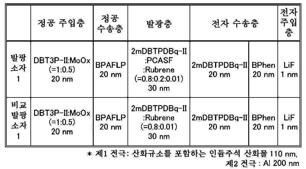
이들 발광 소자를, 질소 분위기의 글로브 박스 내에 있어서, 발광 소자가 대기에 노출되지 않도록 밀봉하는 작업을 행한 후, 발광 소자의 동작 특성에 대하여 측정을 행하였다. 또한, 측정은 실온(25 ℃에서 유지된 분위기)에서 행하였다.These light emitting devices were sealed in a glove box with a nitrogen atmosphere so that the light emitting devices were not exposed to the atmosphere, and then the operating characteristics of the light emitting devices were measured. The measurement was carried out at room temperature (an atmosphere maintained at 25 캜).
발광 소자 1 및 비교 발광 소자 1의 전압-휘도 특성을 도 12에 나타내었다. 도 12에 있어서, 횡축은 전압(V)을 종축은 휘도(cd/㎡)를 나타낸다. 또한, 휘도-전류 효율 특성을 도 13에 나타내었다. 도 13에 있어서, 횡축은 휘도(cd/㎡)를 종축은 전류 효율(cd/A)을 나타낸다. 또한 휘도-전력 효율 특성을 도 14에 도시한다. 도 14에 있어서, 횡축은 휘도(cd/㎡)를, 종축은 전력 효율(lm/W)을 나타낸다. 또한 휘도-외부 양자 효율을 도 15에 도시한다. 도 15에 있어서, 횡축은 휘도(cd/㎡)를 종축은 외부 양자 효율(%)을 나타낸다.The voltage-luminance characteristics of the light-emitting
또한, 발광 소자 1 및 비교 발광 소자 1에 있어서의 휘도 1000 cd/㎡ 부근인 때의 전압(V), 전류 밀도(mA/㎠), CIE 색도 좌표(x, y), 전류 효율(cd/A), 전력 효율(lm/W), 외부 양자 효율(%)을 표 2에 나타내었다.(V), current density (mA / cm2), CIE chromaticity coordinates (x, y), current efficiency (cd / A) at the luminance of about 1000 cd / ), Power efficiency (lm / W), and external quantum efficiency (%) are shown in Table 2.

표 2에 나타내는 바와 같이, 휘도 1000 cd/㎡ 부근인 때의 발광 소자 1의 CIE 색도 좌표는 (x, y)=(0.47, 0.52)이며, 휘도 1000 cd/㎡ 부근인 때의 비교 발광 소자 1의 CIE 색도 좌표는 (x, y)=(0.46, 0.50)였다. 이 결과로부터, 발광 소자 1 및 비교 발광 소자 1은 루브렌에서 유래되는 황색 발광이 얻어진 것을 알았다.As shown in Table 2, the CIE chromaticity coordinates of the light-emitting
표 2, 도 12 내지 도 15로부터 알 수 있는 바와 같이, 발광 소자 1은 비교 발광 소자 1과 비교하여 발광을 개시하는 임계값 전압(발광 개시 전압)이 낮고, 전류 효율, 전력 효율 및 외부 양자 효율에 있어서 높은 값을 나타냈다. 발광층(1113)에 사용한 2mDBTPDBq-II와 PCASF는 여기 착체를 형성하기 위해서, 발광층(1113) 중의 여기 착체의 삼중항 여기 상태의 일부로부터 여기 착체의 일중항 여기 상태가 생성된다. 이 여기 착체의 일중항 여기 상태의 에너지가, 형광을 발하는 재료의 일중항 여기 상태로 이동함으로써, 발광 효율의 향상으로 이어졌다고 생각된다. 또한, 이 여기 착체의 형성의 영향에 의해, 발광 개시 전압이 저하했다고 생각된다.As can be seen from Table 2 and FIGS. 12 to 15, the
본 실시예에 있어서도 실시예 1과 마찬가지로, 열 활성화 지연 형광체와 형광을 발하는 재료를 혼합하여 발광층에 사용한 발광 소자와, 열 활성화 지연 형광을 발하지 않는 재료와 형광을 발하는 재료를 혼합하여 발광층에 사용한 비교 발광 소자를 실제로 제작해 비교한 결과에 대해서, 도 16 내지 도 22를 사용하여 설명한다.Also in this embodiment, as in Example 1, the light-emitting element in which the thermally-activating fluorescent material and the fluorescent material are mixed to form the light-emitting layer, the material that does not emit thermal activation retardation fluorescence, and the material that emits fluorescence are mixed, The results of actually making and comparing light emitting elements will be described with reference to Figs. 16 to 22. Fig.
이하, 발광 소자 2를 열 활성화 지연 형광체와 형광을 발하는 재료를 혼합하여 발광층에 사용한 발광 소자로 한다. 또한 비교 발광 소자 2를 열 활성화 지연 형광을 갖지 않은 재료와 형광을 발하는 재료를 혼합하여 발광층에 사용한 발광 소자로 한다.Hereinafter, the light-emitting
발광 소자 2 및 비교 발광 소자 2에서 사용한 형광을 발하는 재료는, 5,6,11,12-테트라페닐 나프타센(관용명: 루브렌)이다.The fluorescent material used in the light-emitting
발광 소자 2에서는 열 활성화 지연 형광체로서, 여기 착체를 형성하는 조합의 2종의 유기 화합물을 사용하였다. 구체적으로는 제1 유기 화합물로서 4,6-비스[3-(9H-카르바졸-9-일)페닐]피리미딘(약칭: 4,6mCzP2Pm)을 사용하고, 제2 유기 화합물로서 N-(1,1'-비페닐-4-일)-N-[4-(9-페닐-9H-카르바졸-3-일)페닐]-9,9-디메틸-9H-플루오렌-2-아민(약칭: PCBBiF)을 사용하였다.In the light-emitting
비교 발광 소자 2에서는 열 활성화 지연 형광을 발하지 않는 재료로서, 4,6-비스[3-(9H-카르바졸-9-일)페닐]피리미딘(약칭: 4,6mCzP2Pm)을 사용하였다. 즉, 열 활성화 지연 형광을 발하지 않는 재료로서, 발광 소자 2에 있어서의 제1 유기 화합물만을 사용하였다.4,6-bis [3- (9H-carbazol-9-yl) phenyl] pyrimidine (abbreviation: 4,6 mCzP2Pm) was used as the material which does not emit thermal activation delayed fluorescence. That is, only the first organic compound in the light-emitting
본 실시예에서 사용한 재료의 화학식을 이하에 나타내었다.The chemical formula of the material used in this example is shown below.

이하에, 발광 소자 2 및 비교 발광 소자 2의 제작 방법을 나타낸다.Hereinafter, a manufacturing method of the light-emitting
(발광 소자 2)(Light emitting element 2)
우선, 발광 소자 1과 마찬가지의 재료 및 조건에서 유리 기판(1100) 위에 제1 전극(1101), 정공 주입층(1111) 및 정공 수송층(1112)을 형성하였다.First, a
이어서, 4,6mCzP2Pm(약칭), PCBBiF(약칭) 및 루브렌을 공증착하여 정공 수송층(1112) 위에 발광층(1113)을 형성하였다. 여기서, 4,6mCzP2Pm, PCBBiF 및 루브렌의 중량비는, 0.8:0.2:0.0075(=4,6mCzP2Pm:PCBBiF:루브렌)이 되도록 조절하였다. 또한, 발광층(1113)의 막 두께는 40 nm로 하였다.Subsequently, 4,6 mCzP2Pm (abbreviated name), PCBBiF (abbreviation) and rubrene were co-deposited to form a
이어서, 발광층(1113) 위에 4,6mCzP2Pm(약칭)을 막 두께 10 nm가 되도록 성막하여 제1 전자 수송층(1114a)을 형성하였다.Subsequently, 4,6 mCzP2Pm (abbreviation) was deposited on the light-emitting
이어서, 제1 전자 수송층(1114a) 위에 바소페난트롤린(약칭: BPhen)을 막 두께 15 nm가 되도록 성막하여 제2 전자 수송층(1114b)을 형성하였다.Then, a second
또한, 발광 소자 1과 마찬가지의 재료 및 조건에서 전자 주입층(1115) 및 제2 전극을 형성함으로써 본 실시예의 발광 소자 2를 제작하였다.Further, the light-emitting
(비교 발광 소자 2)(Comparative Light-Emitting Element 2)
비교 발광 소자 2의 발광층(1113)은 4,6mCzP2Pm(약칭) 및 루브렌을 공증착함으로써 형성하였다. 여기서, 4,6mCzP2Pm 및 루브렌의 중량비는, 1:0.005(=4,6mCzP2Pm:루브렌)이 되도록 조절하였다. 또한, 발광층(1113)의 막 두께는 40 nm로 하였다. 발광층(1113) 이외에는, 발광 소자 2와 마찬가지로 제작하였다.The
또한, 상술한 증착 과정에 있어서, 증착은 모두 저항 가열법을 사용하였다.Further, in the above-described deposition process, resistance heating method was used for all deposition processes.
이상으로부터 얻어진 발광 소자 2 및 비교 발광 소자 2의 소자 구조를 표 3에 나타내었다.Table 3 shows the device structures of the light-emitting

이들 발광 소자를, 질소 분위기의 글로브 박스 내에 있어서, 발광 소자가 대기에 노출되지 않도록 밀봉하는 작업을 행한 후, 발광 소자의 동작 특성에 대하여 측정을 행하였다. 또한, 측정은 실온(25 ℃에서 유지된 분위기)에서 행하였다.These light emitting devices were sealed in a glove box with a nitrogen atmosphere so that the light emitting devices were not exposed to the atmosphere, and then the operating characteristics of the light emitting devices were measured. The measurement was carried out at room temperature (an atmosphere maintained at 25 캜).
발광 소자 2 및 비교 발광 소자 2의 전압-휘도 특성을 도 16에 나타내었다. 도 16에 있어서, 횡축은 전압(V)을 종축은 휘도(cd/㎡)를 나타낸다. 또한, 휘도-전류 효율 특성을 도 17에 나타내었다. 도 17에 있어서, 횡축은 휘도(cd/㎡)를 종축은 전류 효율(cd/A)을 나타낸다. 또한, 전압-전류 특성을 도 18에 나타내었다. 도 18에 있어서, 횡축은 전압(V)을 종축은 전류(mA)를 나타낸다. 또한, 휘도-전력 효율 특성을 도 19에 나타내었다. 도 19에 있어서, 횡축은 휘도(cd/㎡)를 종축은 전력 효율(lm/W)을 나타낸다. 또한 휘도-외부 양자 효율을 도 20에 나타내었다. 도 20에 있어서, 횡축은 휘도(cd/㎡)를 종축은 외부 양자 효율(%)을 나타낸다.The voltage-luminance characteristics of the light-emitting
또한, 발광 소자 2 및 비교 발광 소자 2에 있어서의 휘도 1000 cd/㎡ 부근인 때의 전압(V), 전류 밀도(mA/㎠), CIE 색도 좌표(x, y), 전류 효율(cd/A), 전력 효율(lm/W), 외부 양자 효율(%)을 표 4에 나타내었다.(V), current density (mA / cm 2), CIE chromaticity coordinates (x, y), current efficiency (cd / A) at a luminance of about 1000 cd /
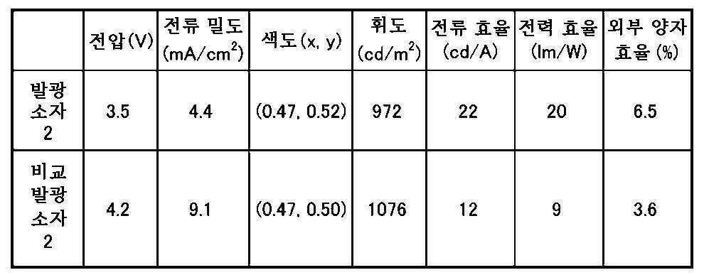
표 4에 나타내는 바와 같이, 휘도 1000 cd/㎡ 부근의 발광 소자 2의 CIE 색도 좌표는 (x, y)=(0.47, 0.52)이며, 휘도 1000 cd/㎡ 부근의 휘도인 때의 비교 발광 소자 2의 CIE 색도 좌표는 (x, y)=(0.47, 0.50)이었다.As shown in Table 4, the CIE chromaticity coordinates of the
또한, 발광 소자 2 및 비교 발광 소자 2에 0.1 mA의 전류를 흘렸을 때의 발광 스펙트럼을 도 21에 나타내었다. 도 21에서는 종축이 발광 강도(임의 단위), 횡축이 파장(nm)을 나타낸다. 발광 강도는 최대 출발 광강도를 1로 한 상대적인 값으로서 나타낸다. 도 21에 나타내는 바와 같이, 발광 소자 2 및 비교 발광 소자 2의 발광 스펙트럼은 558 nm 부근에 최대 발광 파장을 가진 루브렌 유래의 스펙트럼을 나타내고 있고, 표 4의 결과와 아울러, 발광 소자 2 및 비교 발광 소자 2은 노란 발광을 나타내는 발광 소자인 것을 알았다.21 shows the emission spectrum when a current of 0.1 mA was passed through the light-emitting
또한, 초기 휘도를 5000 cd/㎡로 하고, 전류 밀도 일정의 조건으로 발광 소자 2 및 비교 발광 소자 2를 구동하고, 신뢰성 시험을 행한 결과를 도 22에 나타내었다. 도 22에서는, 초기 휘도를 100%로 한 규격화 휘도의 변화를 나타내고 있다.Fig. 22 shows a result of reliability test in which the
표 4, 도 16 내지 도 22의 결과로부터, 발광 소자 2은 비교 발광 소자 2와 비교하여 발광을 개시하는 임계값 전압(발광 개시 전압)이 낮고, 전류 효율, 전력 효율 및 외부 양자 효율에 있어서 높은 값을 나타냈다. 또한 구동 시간에 수반하는 휘도 저하가 작은, 양호한 신뢰성을 갖는 발광 소자인 것을 알았다.From the results of Table 4 and Figs. 16 to 22, it can be seen that the
발광층(1113)에 사용한 4,6mCzP2Pm과 PCBBiF는 여기 착체를 형성하기 때문에, 발광층(1113) 중의 여기 착체의 삼중항 여기 상태의 일부로부터 여기 착체의 일중항 여기 상태가 생성된다. 이 여기 착체의 일중항 여기 상태의 에너지가, 형광을 발하는 재료의 일중항 여기 상태로 이동함으로써, 발광 효율의 향상으로 이어졌다고 생각된다. 또한, 이 여기 착체의 형성의 영향에 의해, 발광 개시 전압이 저하했다고 생각된다.Since 4,6 mCzP2Pm and PCBBiF used in the
본 실시예에 있어서도 실시예 1과 마찬가지로, 열 활성화 지연 형광체와 형광을 발하는 재료를 혼합하여 발광층에 사용한 발광 소자와, 열 활성화 지연 형광을 발하지 않는 재료와 형광을 발하는 재료를 혼합하여 발광층에 사용한 비교 발광 소자를 실제로 제작해 비교한 결과에 대해서, 도 23 내지 도 29를 사용하여 설명한다.Also in this embodiment, as in Example 1, the light-emitting element in which the thermally-activating fluorescent material and the fluorescent material are mixed to form the light-emitting layer, the material that does not emit thermal activation retardation fluorescence, and the material that emits fluorescence are mixed, The results of actual fabrication and comparison of the light emitting device will be described with reference to FIGS. 23 to 29. FIG.
이하, 발광 소자 3을 열 활성화 지연 형광체와 형광을 발하는 재료를 혼합하여 발광층에 사용한 발광 소자로 한다. 또한 비교 발광 소자 3을 열 활성화 지연 형광을 갖지 않은 재료와 형광을 발하는 재료를 혼합하여 발광층에 사용한 발광 소자로 한다.Hereinafter, the light-emitting
발광 소자 3 및 비교 발광 소자 3에서 사용한 형광을 발하는 재료는, 쿠마린6(관용명)이다.The material emitting fluorescence used in the light-emitting
발광 소자 3에서는 열 활성화 지연 형광체로서, 실시예 2와 같은 여기 착체를 형성하는 조합의 2종의 유기 화합물을 사용하였다. 구체적으로는 제1 유기 화합물로서 4,6-비스[3-(9H-카르바졸-9-일)페닐]피리미딘(약칭: 4,6mCzP2Pm)을 사용하고, 제2 유기 화합물로서 N-(1,1'-비페닐-4-일)-N-[4-(9-페닐-9H-카르바졸-3-일)페닐]-9,9-디메틸-9H-플루오렌-2-아민(약칭: PCBBiF)을 사용하였다.In the light-emitting
비교 발광 소자 3에서는 열 활성화 지연 형광을 발하지 않는 재료로서, 실시예 2와 같은 4,6-비스[3-(9H-카르바졸-9-일)페닐]피리미딘(약칭: 4,6mCzP2Pm)을 사용하였다. 즉, 열 활성화 지연 형광을 발하지 않는 재료로서, 발광 소자 3에 있어서의 제1 유기 화합물만을 사용하였다.In the comparative light-emitting
본 실시예에서 사용한 재료의 화학식에 대해서는, 실시예 2의 화학식을 참조하면 된다.With respect to the chemical formula of the material used in this embodiment, reference may be made to the chemical formula of Example 2. [
이하에, 발광 소자 3 및 비교 발광 소자 3의 제작 방법을 나타낸다.Hereinafter, a manufacturing method of the light-emitting
(발광 소자 3)(Light emitting element 3)
우선, 발광 소자 1과 마찬가지의 재료 및 조건에서 유리 기판(1100) 위에 제1 전극(1101), 정공 주입층(1111) 및 정공 수송층(1112)을 형성하였다.First, a
이어서, 4,6mCzP2Pm(약칭), PCBBiF(약칭) 및 쿠마린6을 공증착하여 정공 수송층(1112) 위에 발광층(1113)을 형성하였다. 여기서, 4,6mCzP2Pm, PCBBiF 및 쿠마린6의 중량비는, 0.8:0.2:0.005(=4,6mCzP2Pm:PCBBiF:쿠마린6)이 되도록 조절하였다. 또한, 발광층(1113)의 막 두께는 40 nm로 하였다.Subsequently, 4,6 mCzP2Pm (abbreviation), PCBBiF (abbreviation) and
이어서, 발광층(1113) 위에 4,6mCzP2Pm(약칭)을 막 두께 10 nm가 되도록 성막하여 제1 전자 수송층(1114a)을 형성하였다.Subsequently, 4,6 mCzP2Pm (abbreviation) was deposited on the light-emitting
이어서, 제1 전자 수송층(1114a) 위에 바소페난트롤린(약칭: BPhen)을 막 두께 15 nm가 되도록 성막하여 제2 전자 수송층(1114b)을 형성하였다.Then, a second
또한, 발광 소자 1과 마찬가지의 재료 및 조건에서 전자 주입층(1115) 및 제2 전극을 형성함으로써 본 실시예의 발광 소자 3을 제작하였다.Further, the light-emitting
(비교 발광 소자 3)(Comparative Light-emitting Element 3)
비교 발광 소자 3의 발광층(1113)은 4,6mCzP2Pm(약칭) 및 쿠마린6을 공증착함으로써 형성하였다. 여기서, 4,6mCzP2Pm 및 쿠마린6의 중량비는, 1:0.005(=4,6mCzP2Pm:쿠마린6)이 되도록 조절하였다. 또한, 발광층(1113)의 막 두께는 40 nm로 하였다. 발광층(1113) 이외에는, 발광 소자 3과 마찬가지로 제작하였다.The
또한, 상술한 증착 과정에 있어서, 증착은 모두 저항 가열법을 사용하였다.Further, in the above-described deposition process, resistance heating method was used for all deposition processes.
이상으로부터 얻어진 발광 소자 3 및 비교 발광 소자 3의 소자 구조를 표 5에 나타내었다.The device structures of the light-emitting

이들 발광 소자를, 질소 분위기의 글로브 박스 내에 있어서, 발광 소자가 대기에 노출되지 않도록 밀봉하는 작업을 행한 후, 발광 소자의 동작 특성에 대하여 측정을 행하였다. 또한, 측정은 실온(25 ℃에서 유지된 분위기)에서 행하였다.These light emitting devices were sealed in a glove box with a nitrogen atmosphere so that the light emitting devices were not exposed to the atmosphere, and then the operating characteristics of the light emitting devices were measured. The measurement was carried out at room temperature (an atmosphere maintained at 25 캜).
발광 소자 3 및 비교 발광 소자 3의 전압-휘도 특성을 도 23에 나타내었다. 도 23에 있어서, 횡축은 전압(V)을 종축은 휘도(cd/㎡)를 나타낸다. 또한, 휘도-전류 효율 특성을 도 24에 나타내었다. 도 24에 있어서, 횡축은 휘도(cd/㎡)를 종축은 전류 효율(cd/A)을 나타낸다. 또한, 전압-전류 특성을 도 25에 나타내었다. 도 25에 있어서, 횡축은 전압(V)을 종축은 전류(mA)를 나타낸다. 또한, 휘도-전력 효율 특성을 도 26에 나타내었다. 도 26에 있어서, 횡축은 휘도(cd/㎡)를 종축은 전력 효율(lm/W)을 나타낸다. 또한 휘도-외부 양자 효율을 도 27에 나타내었다. 도 27에 있어서, 횡축은 휘도(cd/㎡)를 종축은 외부 양자 효율(%)을 나타낸다.The voltage-luminance characteristics of the light-emitting
또한, 발광 소자 3 및 비교 발광 소자 3에 있어서의 휘도 1000 cd/㎡ 부근인 때의 전압(V), 전류 밀도(mA/㎠), CIE 색도 좌표(x, y), 전류 효율(cd/A), 전력 효율(lm/W), 외부 양자 효율(%)을 표 6에 나타내었다.(V), current density (mA / cm 2), CIE chromaticity coordinates (x, y), current efficiency (cd / A) at the luminance of about 1000 cd /

표 6에 나타내는 바와 같이, 휘도 1000 cd/㎡ 부근의 발광 소자 3의 CIE 색도 좌표는 (x, y)=(0.28, 0.60)이며, 휘도 1000 cd/㎡ 부근의 휘도인 때의 비교 발광 소자 3의 CIE 색도 좌표는 (x, y)=(0.26, 0.58)이었다.As shown in Table 6, the CIE chromaticity coordinates of the
또한, 발광 소자 3 및 비교 발광 소자 3에 0.1 mA의 전류를 흘렸을 때의 발광 스펙트럼을 도 28에 나타내었다. 도 28에서는 종축이 발광 강도(임의 단위), 횡축이 파장(nm)을 나타낸다. 발광 강도는 최대 출발 광강도를 1로 한 상대적인 값으로서 나타낸다. 도 28에 나타내는 바와 같이, 발광 소자 3 및 비교 발광 소자 3의 발광 스펙트럼은 500 nm 부근에 최대 발광 파장을 가진 쿠마린6 유래의 스펙트럼을 나타내고 있어, 표 6의 결과와 아울러, 발광 소자 3 및 비교 발광 소자 3은 녹색의 발광을 나타내는 발광 소자인 것을 알았다.28 shows the emission spectrum when a current of 0.1 mA was passed through the light-emitting
또한, 초기 휘도를 5000 cd/㎡로 하고, 전류 밀도 일정의 조건으로 발광 소자 3 및 비교 발광 소자 3을 구동하고, 신뢰성 시험을 행한 결과를 도 29에 나타내었다. 도 29에서는, 초기 휘도를 100%로 한 규격화 휘도의 변화를 나타내고 있다.29 shows the results of the reliability test in which the
표 6, 도 23 내지 도 29의 결과로부터, 발광 소자 3은 비교 발광 소자 3과 비교하여 발광을 개시하는 임계값 전압(발광 개시 전압)이 낮고, 전류 효율, 전력 효율 및 외부 양자 효율에 있어서 높은 값을 나타냈다. 또한 구동 시간에 수반하는 휘도 저하가 작은, 양호한 신뢰성을 갖는 발광 소자인 것을 알았다.From the results shown in Table 6 and Figs. 23 to 29, the
발광층(1113)에 사용한 4,6mCzP2Pm과 PCBBiF는 여기 착체를 형성하기 위해서, 발광층(1113) 중의 여기 착체의 삼중항 여기 상태의 일부로부터 여기 착체의 일중항 여기 상태가 생성된다. 이 여기 착체의 일중항 여기 상태의 에너지가, 형광을 발하는 재료의 일중항 여기 상태로 이동함으로써, 발광 효율의 향상으로 이어졌다고 생각된다. 또한, 이 여기 착체의 형성의 영향에 의해 발광 개시 전압이 저하했다고 생각된다.The singlet excited state of the excited complex is generated from a part of the triplet excited state of the excited complex in the
본 실시예에 있어서도 실시예 1과 마찬가지로, 열 활성화 지연 형광체와 형광을 발하는 재료를 혼합하여 발광층에 사용한 발광 소자와, 열 활성화 지연 형광을 발하지 않는 재료와 형광을 발하는 재료를 혼합하여 발광층에 사용한 비교 발광 소자를 실제로 제작해 비교한 결과에 대해서, 도 30 내지 도 35를 사용하여 설명한다.Also in this embodiment, as in Example 1, the light-emitting element in which the thermally-activating fluorescent material and the fluorescent material are mixed to form the light-emitting layer, the material that does not emit thermal activation retardation fluorescence, and the material that emits fluorescence are mixed, The results of actually making and comparing light emitting elements will be described with reference to Figs. 30 to 35. Fig.
이하, 발광 소자 4를 열 활성화 지연 형광체와 형광을 발하는 재료를 혼합하여 발광층에 사용한 발광 소자로 한다. 또한 비교 발광 소자 4를 열 활성화 지연 형광을 갖지 않은 재료와 형광을 발하는 재료를 혼합하여 발광층에 사용한 발광 소자로 한다.Hereinafter, the light-emitting
발광 소자 3 및 비교 발광 소자 3에서 사용한 형광을 발하는 재료는, {2-tert-부틸-6-[2-(1,1,7,7-테트라메틸-2,3,6,7-테트라히드로-1H,5H-벤조[ij]퀴놀리진-9-일)에테닐]-4H-피란-4-일리덴}프로판 디니트릴(약칭:DCJTB)이다.The fluorescent material used in the
발광 소자 4에서는 열 활성화 지연 형광체로서, 실시예 2와 같은 여기 착체를 형성하는 조합의 2종의 유기 화합물을 사용하였다. 구체적으로는 제1 유기 화합물로서 4,6-비스[3-(9H-카르바졸-9-일)페닐]피리미딘(약칭: 4,6mCzP2Pm)을 사용하고, 제2 유기 화합물로서 N-(1,1'-비페닐-4-일)-N-[4-(9-페닐-9H-카르바졸-3-일)페닐]-9,9-디메틸-9H-플루오렌-2-아민(약칭: PCBBiF)을 사용하였다.In the light-emitting
비교 발광 소자 4에서는 열 활성화 지연 형광을 발하지 않는 재료로서, 실시예 2와 같은 4,6-비스[3-(9H-카르바졸-9-일)페닐]피리미딘(약칭: 4,6mCzP2Pm)을 사용하였다. 즉, 열 활성화 지연 형광을 발하지 않는 재료로서, 발광 소자 4에 있어서의 제1 유기 화합물만을 사용하였다.In the comparative light-emitting
본 실시예에서 사용한 재료의 화학식에 대해서는, 실시예 2의 화학식을 참조하면 된다.With respect to the chemical formula of the material used in this embodiment, reference may be made to the chemical formula of Example 2. [
이하에, 발광 소자 4 및 비교 발광 소자 4의 제작 방법을 나타낸다.Hereinafter, a manufacturing method of the light-emitting
(발광 소자 4)(Light emitting element 4)
우선, 발광 소자 1과 마찬가지의 재료 및 조건에서 유리 기판(1100) 위에 제1 전극(1101), 정공 주입층(1111) 및 정공 수송층(1112)을 형성하였다.First, a
이어서, 4,6mCzP2Pm(약칭), PCBBiF(약칭) 및 DCJTB(약칭)를 공증착하여 정공 수송층(1112) 위에 발광층(1113)을 형성하였다. 여기서, 4,6mCzP2Pm, PCBBiF 및 DCJTB의 중량비는, 0.8:0.2:0.005(=4,6mCzP2Pm: PCBBiF:DCJTB)가 되도록 조절하였다. 또한, 발광층(1113)의 막 두께는 40 nm로 하였다.Subsequently, 4,6mCzP2Pm (abbreviation), PCBBiF (abbreviation) and DCJTB (abbreviation) were co-deposited to form a
이어서, 발광층(1113) 위에 4,6mCzP2Pm(약칭)을 막 두께 10 nm가 되도록 성막하여 제1 전자 수송층(1114a)을 형성하였다.Subsequently, 4,6 mCzP2Pm (abbreviation) was deposited on the light-emitting
이어서, 제1 전자 수송층(1114a) 위에 바소페난트롤린(약칭: BPhen)을 막 두께 15 nm가 되도록 성막하여 제2 전자 수송층(1114b)을 형성하였다.Then, a second
또한, 발광 소자 1과 마찬가지의 재료 및 조건에서 전자 주입층(1115) 및 제2 전극을 형성함으로써 본 실시예의 발광 소자 4를 제작하였다.In addition, the light-emitting
(비교 발광 소자 4)(Comparative Light-emitting Element 4)
비교 발광 소자 3의 발광층(1113)은 4,6mCzP2Pm(약칭) 및 DCJTB(약칭)를 공증착함으로써 형성하였다. 여기서, 4,6mCzP2Pm 및 DCJTB의 중량비는, 1:0.005(=4,6mCzP2Pm:DCJTB)가 되도록 조절하였다. 또한, 발광층(1113)의 막 두께는 40 nm로 하였다. 발광층(1113) 이외에는, 발광 소자 4과 마찬가지로 제작하였다.The
또한, 상술한 증착 과정에 있어서, 증착은 모두 저항 가열법을 사용하였다.Further, in the above-described deposition process, resistance heating method was used for all deposition processes.
이상으로부터 얻어진 발광 소자 4 및 비교 발광 소자 4의 소자 구조를 표 7에 나타내었다.The device structures of the light-emitting

이들 발광 소자를, 질소 분위기의 글로브 박스 내에 있어서, 발광 소자가 대기에 노출되지 않도록 밀봉하는 작업을 행한 후, 발광 소자의 동작 특성에 대하여 측정을 행하였다. 또한, 측정은 실온(25 ℃에서 유지된 분위기)에서 행하였다.These light emitting devices were sealed in a glove box with a nitrogen atmosphere so that the light emitting devices were not exposed to the atmosphere, and then the operating characteristics of the light emitting devices were measured. The measurement was carried out at room temperature (an atmosphere maintained at 25 캜).
발광 소자 3 및 비교 발광 소자 3의 전압-휘도 특성을 도 30에 나타내었다. 도 30에 있어서, 횡축은 전압(V)을 종축은 휘도(cd/㎡)를 나타낸다. 또한, 휘도-전류 효율 특성을 도 31에 나타내었다. 도 31에 있어서, 횡축은 휘도(cd/㎡)를 종축은 전류 효율(cd/A)을 나타낸다. 또한, 전압-전류 특성을 도 32에 나타내었다. 도 32에 있어서, 횡축은 전압(V)을 종축은 전류(mA)를 나타낸다. 또한, 휘도-전력 효율 특성을 도 33에 나타내었다. 도 33에 있어서, 횡축은 휘도(cd/㎡)를 종축은 전력 효율(lm/W)을 나타낸다. 또한 휘도-외부 양자 효율을 도 34에 나타내었다. 도 34에 있어서, 횡축은 휘도(cd/㎡)를 종축은 외부 양자 효율(%)을 나타낸다.The voltage-luminance characteristics of the light-emitting
또한, 발광 소자 4 및 비교 발광 소자 4에 있어서의 휘도 1000 cd/㎡ 부근인 때의 전압(V), 전류 밀도(mA/㎠), CIE 색도 좌표(x, y), 전류 효율(cd/A), 전력 효율(lm/W), 외부 양자 효율(%)을 표 8에 나타내었다.(V), current density (mA / cm2), CIE chromaticity coordinates (x, y), current efficiency (cd / A) at the luminance of about 1000 cd / ), Power efficiency (lm / W), and external quantum efficiency (%) are shown in Table 8.

표 8에 나타내는 바와 같이, 휘도 1000 cd/㎡ 부근의 발광 소자 4의 CIE 색도 좌표는 (x, y)=(0.57, 0.43)이며, 휘도 1000 cd/㎡ 부근의 휘도인 때의 비교 발광 소자 4의 CIE 색도 좌표는 (x, y)=(0.56, 0.41)이었다.As shown in Table 8, the CIE chromaticity coordinates of the
또한, 발광 소자 4 및 비교 발광 소자 4에 0.1 mA의 전류를 흘렸을 때의 발광 스펙트럼을 도 35에 나타내었다. 도 35에서는 종축이 발광 강도(임의 단위), 횡축이 파장(nm)을 나타낸다. 발광 강도는 최대 출발 광강도를 1로 한 상대적인 값으로서 나타낸다. 도 35에 나타내는 바와 같이, 발광 소자 4 및 비교 발광 소자 4의 발광 스펙트럼은 595 nm 부근에 최대 발광 파장을 가진 DCJTB 유래의 스펙트럼을 나타내고 있어, 표 8의 결과와 아울러, 발광 소자 4 및 비교 발광 소자 4은 노란 발광을 나타내는 발광 소자인 것을 알았다.35 shows the emission spectrum when a current of 0.1 mA was passed through the light-emitting
또한, 초기 휘도를 5000 cd/㎡로 하고, 전류 밀도 일정의 조건으로 발광 소자 4 및 비교 발광 소자 4를 구동하고, 신뢰성 시험을 행한 결과를 도 36에 나타내었다. 도 36에서는, 초기 휘도를 100%로 한 규격화 휘도의 변화를 나타내고 있다.Fig. 36 shows the result of reliability test in which the
표 8, 도 30 내지 도 36의 결과로부터, 발광 소자 4은 비교 발광 소자 4과 비교하여 발광을 개시하는 임계값 전압(발광 개시 전압)이 낮고, 전류 효율, 전력 효율 및 외부 양자 효율에 있어서 높은 값을 나타냈다. 또한 구동 시간에 수반하는 휘도 저하가 작은, 양호한 신뢰성을 갖는 발광 소자인 것을 알았다.From the results of Table 8 and FIG. 30 to FIG. 36, it can be seen that the
발광층(1113)에 사용한 4,6mCzP2Pm과 PCBBiF는 여기 착체를 형성하기 위해서, 발광층(1113) 중의 여기 착체의 삼중항 여기 상태의 일부로부터 여기 착체의 일중항 여기 상태가 생성된다. 이 여기 착체의 일중항 여기 상태의 에너지가, 형광을 발하는 재료의 일중항 여기 상태로 이동함으로써, 발광 효율의 향상으로 이어졌다고 생각된다. 또한, 이 여기 착체의 형성의 영향에 의해, 발광 개시 전압이 저하했다고 생각된다.The singlet excited state of the excited complex is generated from a part of the triplet excited state of the excited complex in the
101: 전극
102: 전극
103: EL층
111: 정공 주입층
112: 정공 수송층
113: 발광층
113A: 발광 물질
113D: 열 활성화 지연 형광체
113D1: 유기 화합물
113D2: 유기 화합물
114: 전자 수송층
115: 전자 주입층
400: 기판
401: 전극
402: 보조 전극
403: EL층
404: 전극
405: 시일재
406: 시일재
407: 밀봉 기판
412: 패드
420: IC칩
951: 기판
952: 전극
953: 절연층
954: 격벽층
955: EL층
956: 전극
1001: 기판
1002: 하지 절연막
1003: 게이트 절연막
1006: 게이트 전극
1007: 게이트 전극
1008: 게이트 전극
1020: 층간 절연막
1021: 층간 절연막
1022: 전극
1024R 전극
1024G: 전극
1024B: 전극
1024W: 전극
1025: 격벽
1028: EL층
1029: 전극
1031: 밀봉 기판
1032a: 시일재
1032b: 시일재
1033: 기재
1034B: 착색층
1034G: 착색층
1034R: 착색층
1036: 오버코트층
1037: 층간 절연막
1040: 화소부
1041: 구동 회로부
1042: 주변부
1044B: 발광 영역
1044G: 발광 영역
1044R: 발광 영역
1044W: 발광 영역
1100: 기판
1101: 전극
1103: 전극
1111: 정공 주입층
1112: 정공 수송층
1113: 발광층
1114a: 전자 수송층
1114b: 전자 수송층
1115: 전자 주입층
2001: 하우징
2002: 광원
2003: 전기 스탠드
3001: 조명 장치
5000: 표시
5001: 표시
5002: 표시
5003: 표시
5004: 표시
5005: 표시
5021: 바늘
5022: 표시부
7101: 하우징
7103: 표시부
7105: 설치구(부재)
7107: 표시부
7109: 조작 키
7110: 리모콘 조작기
7201: 본체
7202: 하우징
7203: 표시부
7204: 키보드
7205: 외부 접속 포트
7206: 포인팅 디바이스
7210: 표시부
7301: 하우징
7302: 하우징
7303: 연결부
7304: 표시부
7305: 표시부
7306: 스피커부
7307: 기록 매체 삽입부
7308: LED 램프
7309: 조작 키
7310: 접속 단자
7311: 센서
7312: 마이크로폰
7400: 휴대 전화기
7401: 하우징
7402: 표시부
7403: 조작 버튼
7404: 외부 접속 포트
7405: 스피커
7406: 마이크101: Electrode
102: electrode
103: EL layer
111: Hole injection layer
112: hole transport layer
113: light emitting layer
113A: luminescent material
113D: Thermal activation retarding phosphor
113D1: Organic compounds
113D2: Organic compounds
114: electron transport layer
115: electron injection layer
400: substrate
401: electrode
402: auxiliary electrode
403: EL layer
404: Electrode
405: Seal material
406: Seal material
407: sealing substrate
412: Pad
420: IC chip
951: substrate
952: Electrode
953: insulating layer
954: partition wall layer
955: EL layer
956: Electrode
1001: substrate
1002:
1003: Gate insulating film
1006: gate electrode
1007: gate electrode
1008: gate electrode
1020: Interlayer insulating film
1021: Interlayer insulating film
1022: electrode
1024R electrode
1024G: Electrode
1024B: Electrode
1024W: Electrode
1025:
1028: EL layer
1029: Electrode
1031: sealing substrate
1032a: sealing material
1032b:
1033: Equipment
1034B: colored layer
1034G: colored layer
1034R: colored layer
1036: Overcoat layer
1037: Interlayer insulating film
1040:
1041:
1042:
1044B:
1044G: light emitting region
1044R: light emitting region
1044W: light emitting region
1100: substrate
1101: electrode
1103: Electrode
1111: Hole injection layer
1112: Hole transport layer
1113: light emitting layer
1114a: electron transport layer
1114b: electron transport layer
1115: electron injection layer
2001: Housing
2002: Light source
2003: Electric stand
3001: Lighting system
5000: Display
5001: Display
5002: Display
5003: Display
5004: Show
5005: Show
5021: Needle
5022:
7101: Housing
7103:
7105: Mounting hole (member)
7107:
7109: Operation keys
7110: Remote controller
7201:
7202: Housings
7203:
7204: Keyboard
7205: External connection port
7206: Pointing device
7210:
7301: Housing
7302: Housing
7303: Connection
7304:
7305:
7306:
7307: recording medium insertion portion
7308: LED lamp
7309: Operation keys
7310: Connection terminal
7311: Sensor
7312: microphone
7400: Mobile phone
7401: Housing
7402:
7403: Operation button
7404: External connection port
7405: Speaker
7406: Microphone
Claims (16)
열 활성화 지연 형광체(thermally activated delayed fluorescent substance) 및 형광을 발하는 재료를 포함하고,
상기 열 활성화 지연 형광체의 삼중항 여기 상태의 준위로부터 상기 열 활성화 지연 형광체의 일중항 여기 상태의 준위로 에너지가 이동하고,
상기 열 활성화 지연 형광체의 일중항 여기 상태의 준위로부터 상기 형광을 발하는 재료의 흡수 스펙트럼에 있어서 최장파장 측에 나타나는 흡수대를 거쳐서, 상기 형광을 발하는 재료의 일중항 여기 상태의 준위로 에너지가 이동하고,
상기 형광을 발하는 재료의 일중항 여기 상태의 준위로부터 형광을 발하는, 발광 장치.As a light emitting device,
A thermally activated delayed fluorescent substance and a fluorescent material,
Energy is shifted from the triplet excited state of the thermal activation retardation phosphor to the singlet excited state of the thermal activation retardation phosphor,
The energy is shifted from the level of the singly excited state of the thermal activation retardation phosphor to the singlet excited state level of the material emitting the fluorescence through the absorption band appearing on the longest wavelength side in the absorption spectrum of the material emitting the fluorescence,
And emits fluorescence from the singlet excited state level of the fluorescent material.
상기 열 활성화 지연 형광체의 삼중항 여기 상태의 준위로부터 상기 열 활성화 지연 형광체의 일중항 여기 상태의 준위로의 에너지 이동은 역항간 교차에 의한 것인, 발광 장치.The method according to claim 1,
Wherein energy transfer from the triplet excited state level of the thermal activation retardation phosphor to the level of the singly excited state of the thermal activation retardation phosphor is caused by crossing of the inverse term.
상기 열 활성화 지연 형광체는 일중항 여기 상태와 삼중항 여기 상태의 에너지 차가 0eV 이상 0.2eV 이하인, 발광 장치.The method according to claim 1,
And the energy difference between the singly excited state and the triplet excited state of the thermal activation retardation fluorescent material is 0 eV or more and 0.2 eV or less.
상기 열 활성화 지연 형광체의 발광 스펙트럼과, 상기 형광을 발하는 재료의 흡수 스펙트럼에 있어서 최장파장 측에 나타나는 흡수대가 중첩되는, 발광 장치.The method according to claim 1,
And the absorption band appearing on the longest wavelength side in the absorption spectrum of the material emitting the fluorescence overlaps with the emission spectrum of the thermal activation delayed fluorescent substance.
상기 열 활성화 지연 형광체의 발광 스펙트럼의 피크 파장과 상기 형광을 발하는 재료의 발광 스펙트럼의 피크 파장의 차가 30nm 이내인, 발광 장치.The method according to claim 1,
Wherein the difference between the peak wavelength of the luminescence spectrum of the thermal activation retardation phosphor and the peak wavelength of the luminescence spectrum of the material emitting the fluorescence is within 30 nm.
제1 유기 화합물, 제2 유기 화합물, 및 형광을 발하는 재료를 포함하는 발광층을 포함하고,
상기 제1 유기 화합물 및 상기 제2 유기 화합물은 여기 착체를 형성하는 조합이고,
상기 여기 착체의 삼중항 여기 상태의 준위로부터 상기 여기 착체의 일중항 여기 상태의 준위로 에너지가 이동하고,
상기 여기 착체의 일중항 여기 상태의 준위로부터 상기 형광을 발하는 재료의 일중항 여기 상태의 준위로 에너지가 이동하고,
상기 형광을 발하는 재료의 일중항 여기 상태의 준위로부터 형광을 발하는, 발광 장치.As a light emitting device,
A light-emitting layer comprising a first organic compound, a second organic compound, and a fluorescent material,
Wherein the first organic compound and the second organic compound are combinations that form an excited complex,
Energy is transferred from the triplet excited state level of the excited complex to the singlet excited state level of the excited complex,
Energy is transferred from the singlet excited state level of the excited complex to the singlet excited state level of the material emitting the fluorescence,
And emits fluorescence from the singlet excited state level of the fluorescent material.
상기 여기 착체의 삼중항 여기 상태의 준위로부터 상기 여기 착체의 일중항 여기 상태의 준위로의 에너지 이동은 역항간 교차에 의한 것인, 발광 장치.The method according to claim 6,
Wherein the energy transfer from the triplet excited state level of the excited complex to the singlet excited state level of the excited complex is due to inverse crossing.
상기 여기 착체는 일중항 여기 상태와 삼중항 여기 상태의 에너지 차가 0eV 이상 0.2eV 이하인, 발광 장치.The method according to claim 6,
Wherein the excited complex has an energy difference between singlet excited state and triplet excited state of 0 eV to 0.2 eV.
상기 여기 착체의 발광 스펙트럼과, 상기 형광을 발하는 재료의 흡수 스펙트럼에 있어서 최장파장 측에 나타나는 흡수대가 중첩되는, 발광 장치.The method according to claim 6,
And the absorption band appearing on the longest wavelength side in the absorption spectrum of the material emitting the fluorescence overlaps with the emission spectrum of the excited complex.
상기 여기 착체의 발광 스펙트럼의 피크 파장은 상기 형광을 발하는 재료의 흡수 스펙트럼에 있어서 최장파장 측에 나타나는 흡수대의 피크 파장 이상인, 발광 장치.10. The method of claim 9,
Wherein the peak wavelength of the luminescence spectrum of the excited complex is at least the peak wavelength of the absorption band appearing on the longest wavelength side in the absorption spectrum of the material emitting the fluorescence.
상기 여기 착체의 발광 스펙트럼의 피크는 상기 형광을 발하는 재료의 발광 스펙트럼의 피크의 +30㎚ 이내인, 발광 장치.The method according to claim 6,
And the peak of the luminescence spectrum of the excited complex is within +30 nm of the peak of the luminescence spectrum of the material emitting the fluorescence.
상기 여기 착체의 발광 스펙트럼의 피크는 상기 형광을 발하는 재료의 발광 스펙트럼의 피크의 -30㎚ 이내인, 발광 장치.The method according to claim 6,
And the peak of the luminescence spectrum of the excited complex is within -30 nm of the peak of the luminescence spectrum of the material emitting the fluorescence.
상기 여기 착체의 발광 스펙트럼의 피크 파장의 에너지 환산값은 상기 형광을 발하는 재료의 발광의 피크 파장의 에너지 환산값의 +0.2eV 이하인, 발광 장치.The method according to claim 6,
Wherein the energy conversion value of the peak wavelength of the emission spectrum of the excited complex is +0.2 eV or less of the energy conversion value of the peak wavelength of the emission of the fluorescent material.
상기 여기 착체의 발광 스펙트럼의 피크 파장의 에너지 환산값은 상기 형광을 발하는 재료의 발광의 피크 파장의 에너지 환산값의 -0.2eV 이상인, 발광 장치.The method according to claim 6,
Wherein the energy conversion value of the peak wavelength of the emission spectrum of the excited complex is -0.2 eV or more of the energy conversion value of the peak wavelength of the emission of the fluorescent material.
상기 열 활성화 지연 형광체의 삼중항 여기 상태의 준위로부터 상기 열 활성화 지연 형광체의 일중항 여기 상태의 준위로 에너지가 이동하고,
상기 열 활성화 지연 형광체의 일중항 여기 상태의 준위로부터 상기 형광을 발하는 재료의 흡수 스펙트럼에 있어서 최장파장 측에 나타나는 흡수대를 거쳐서, 상기 형광을 발하는 재료의 일중항 여기 상태의 준위로 에너지가 이동하고,
상기 형광을 발하는 재료의 일중항 여기 상태의 준위로부터 형광을 발하는, 발광 방법.A light-emitting method in a light-emitting device comprising a thermally-activatable retarding phosphor and a material emitting fluorescence,
Energy is shifted from the triplet excited state of the thermal activation retardation phosphor to the singlet excited state of the thermal activation retardation phosphor,
The energy is shifted from the level of the singly excited state of the thermal activation retardation phosphor to the singlet excited state level of the material emitting the fluorescence through the absorption band appearing on the longest wavelength side in the absorption spectrum of the material emitting the fluorescence,
And emits fluorescence from the singlet excited state level of the fluorescent material.
상기 여기 착체의 삼중항 여기 상태의 준위로부터 상기 여기 착체의 일중항 여기 상태의 준위로 에너지가 이동하고,
상기 여기 착체의 일중항 여기 상태의 준위로부터 상기 형광을 발하는 재료의 일중항 여기 상태의 준위로 에너지가 이동하고,
상기 형광을 발하는 재료의 일중항 여기 상태의 준위로부터 형광을 발하는, 발광 방법.A light emitting method in a light emitting device comprising a first organic compound, a second organic compound forming an excited complex together with the first organic compound, and a light emitting layer containing a fluorescent material,
Energy is transferred from the triplet excited state level of the excited complex to the singlet excited state level of the excited complex,
Energy is transferred from the singlet excited state level of the excited complex to the singlet excited state level of the material emitting the fluorescence,
And emits fluorescence from the singlet excited state level of the fluorescent material.
Priority Applications (1)
| Application Number | Priority Date | Filing Date | Title |
|---|---|---|---|
| KR1020210008941A KR102440283B1 (en) | 2012-08-03 | 2021-01-21 | Light-emitting element |
Applications Claiming Priority (2)
| Application Number | Priority Date | Filing Date | Title |
|---|---|---|---|
| JP2012172830 | 2012-08-03 | ||
| JPJP-P-2012-172830 | 2012-08-03 |
Related Parent Applications (1)
| Application Number | Title | Priority Date | Filing Date |
|---|---|---|---|
| KR1020180132276A Division KR102207668B1 (en) | 2012-08-03 | 2018-10-31 | Light-emitting element |
Related Child Applications (1)
| Application Number | Title | Priority Date | Filing Date |
|---|---|---|---|
| KR1020210008941A Division KR102440283B1 (en) | 2012-08-03 | 2021-01-21 | Light-emitting element |
Publications (2)
| Publication Number | Publication Date |
|---|---|
| KR20180133352A true KR20180133352A (en) | 2018-12-14 |
| KR102208540B1 KR102208540B1 (en) | 2021-01-28 |
Family
ID=50024594
Family Applications (7)
| Application Number | Title | Priority Date | Filing Date |
|---|---|---|---|
| KR1020130091374A KR102014549B1 (en) | 2012-08-03 | 2013-08-01 | Light-emitting element |
| KR1020180132276A KR102207668B1 (en) | 2012-08-03 | 2018-10-31 | Light-emitting element |
| KR1020180155052A KR102208540B1 (en) | 2012-08-03 | 2018-12-05 | Light-emitting element |
| KR1020210008941A KR102440283B1 (en) | 2012-08-03 | 2021-01-21 | Light-emitting element |
| KR1020220110026A KR102481960B1 (en) | 2012-08-03 | 2022-08-31 | Light-emitting element |
| KR1020220181943A KR102676322B1 (en) | 2012-08-03 | 2022-12-22 | Light-emitting element |
| KR1020240077139A KR20240093436A (en) | 2012-08-03 | 2024-06-13 | Light-emitting element |
Family Applications Before (2)
| Application Number | Title | Priority Date | Filing Date |
|---|---|---|---|
| KR1020130091374A KR102014549B1 (en) | 2012-08-03 | 2013-08-01 | Light-emitting element |
| KR1020180132276A KR102207668B1 (en) | 2012-08-03 | 2018-10-31 | Light-emitting element |
Family Applications After (4)
| Application Number | Title | Priority Date | Filing Date |
|---|---|---|---|
| KR1020210008941A KR102440283B1 (en) | 2012-08-03 | 2021-01-21 | Light-emitting element |
| KR1020220110026A KR102481960B1 (en) | 2012-08-03 | 2022-08-31 | Light-emitting element |
| KR1020220181943A KR102676322B1 (en) | 2012-08-03 | 2022-12-22 | Light-emitting element |
| KR1020240077139A KR20240093436A (en) | 2012-08-03 | 2024-06-13 | Light-emitting element |
Country Status (5)
| Country | Link |
|---|---|
| US (9) | US9276228B2 (en) |
| JP (16) | JP2014045179A (en) |
| KR (7) | KR102014549B1 (en) |
| CN (3) | CN103579530B (en) |
| TW (7) | TWI650399B (en) |
Families Citing this family (93)
| Publication number | Priority date | Publication date | Assignee | Title |
|---|---|---|---|---|
| KR20240100473A (en) * | 2011-04-07 | 2024-07-01 | 가부시키가이샤 한도오따이 에네루기 켄큐쇼 | Light-emitting element |
| KR101803537B1 (en) | 2012-02-09 | 2017-11-30 | 가부시키가이샤 한도오따이 에네루기 켄큐쇼 | Light-emitting element |
| DE112013007607B3 (en) * | 2012-03-14 | 2018-02-08 | Semiconductor Energy Laboratory Co., Ltd. | Light emitting device, electronic device and lighting device |
| KR101419810B1 (en) * | 2012-04-10 | 2014-07-15 | 서울대학교산학협력단 | Organic light-emitting diode comprising exciplex forming co-host |
| CN107039593B (en) | 2012-04-20 | 2019-06-04 | 株式会社半导体能源研究所 | Light-emitting component, light emitting device, electronic equipment and lighting device |
| KR20210008947A (en) | 2012-04-20 | 2021-01-25 | 가부시키가이샤 한도오따이 에네루기 켄큐쇼 | Light-emitting element, light-emitting device, electronic appliance, and lighting device |
| TWI651878B (en) | 2012-08-03 | 2019-02-21 | 日商半導體能源研究所股份有限公司 | Light-emitting element, light-emitting device, display device, electronic device and lighting device |
| TWI650399B (en) * | 2012-08-03 | 2019-02-11 | 日商半導體能源研究所股份有限公司 | Light-emitting element |
| JP6312960B2 (en) * | 2012-08-03 | 2018-04-18 | 株式会社半導体エネルギー研究所 | Light emitting element, light emitting device, electronic device, lighting device, and heterocyclic compound |
| ES2661409T3 (en) | 2013-03-29 | 2018-03-28 | Kyulux, Inc. | Organic electroluminescent device |
| US10043982B2 (en) | 2013-04-26 | 2018-08-07 | Semiconductor Energy Laboratory Co., Ltd. | Light-emitting element, light-emitting device, display device, electronic device, and lighting device |
| JP6545934B2 (en) | 2013-06-28 | 2019-07-17 | 株式会社半導体エネルギー研究所 | Light emitting element, lighting device, light emitting device, and electronic device |
| KR102290674B1 (en) | 2013-08-26 | 2021-08-19 | 가부시키가이샤 한도오따이 에네루기 켄큐쇼 | Light-emitting element, light-emitting device, display device, lighting device, and electronic appliance |
| US10014487B2 (en) | 2013-09-17 | 2018-07-03 | Kyulux, Inc. | Organic electroluminescent device |
| CN108630826B (en) | 2013-12-02 | 2021-12-10 | 株式会社半导体能源研究所 | Light emitting element |
| JP5905916B2 (en) * | 2013-12-26 | 2016-04-20 | 出光興産株式会社 | Organic electroluminescence device and electronic device |
| TWI715527B (en) | 2014-02-21 | 2021-01-11 | 日商半導體能源研究所股份有限公司 | Light-emitting element, light-emitting device, electronic device, and lighting device |
| US11611046B2 (en) | 2014-03-13 | 2023-03-21 | Merck Patent Gmbh | Organic electroluminescent device |
| US20170092875A1 (en) * | 2014-03-18 | 2017-03-30 | Merck Patent Gmbh | Organic electroluminescent device |
| TWI729649B (en) | 2014-05-30 | 2021-06-01 | 日商半導體能源研究所股份有限公司 | Light-emitting element, light-emitting device, electronic device, and lighting device |
| DE102015213426B4 (en) * | 2014-07-25 | 2022-05-05 | Semiconductor Energy Laboratory Co.,Ltd. | Light-emitting element, light-emitting device, electronic device, lighting device, and organic compound |
| JP6367340B2 (en) * | 2014-08-22 | 2018-08-01 | シャープ株式会社 | ORGANIC ELECTROLUMINESCENT DEVICE, ITS MANUFACTURING METHOD, AND LIGHT EMITTING METHOD |
| KR102353647B1 (en) * | 2014-08-29 | 2022-01-20 | 가부시키가이샤 한도오따이 에네루기 켄큐쇼 | Light-emitting element, display device, electronic device, and lighting device |
| KR20230051628A (en) * | 2014-09-30 | 2023-04-18 | 가부시키가이샤 한도오따이 에네루기 켄큐쇼 | Light-emitting element, display device, electronic device, and lighting device |
| KR102409803B1 (en) * | 2014-10-10 | 2022-06-17 | 가부시키가이샤 한도오따이 에네루기 켄큐쇼 | Light-emitting element, display device, electronic device, and lighting device |
| JP6494079B2 (en) * | 2014-10-31 | 2019-04-03 | 国立大学法人九州大学 | Organic light emitting device |
| US9957280B2 (en) | 2014-12-15 | 2018-05-01 | Samsung Electronics Co., Ltd. | Luminescent compound and electroluminescent device exhibiting thermally activated delayed fluorescence |
| KR101706752B1 (en) * | 2015-02-17 | 2017-02-27 | 서울대학교산학협력단 | Organic light-emitting device comprising delayed fluorescent host, phosphorescent dopant and fluorescent dopant |
| US10903440B2 (en) | 2015-02-24 | 2021-01-26 | Semiconductor Energy Laboratory Co., Ltd. | Light-emitting element, light-emitting device, electronic device, and lighting device |
| US10062861B2 (en) * | 2015-02-24 | 2018-08-28 | Semiconductor Energy Laboratory Co., Ltd. | Light-emitting element, display device, electronic device, and lighting device |
| TWI779405B (en) | 2015-03-09 | 2022-10-01 | 日商半導體能源研究所股份有限公司 | Light-emitting element, display device, electronic device, and lighting device |
| TWI704706B (en) * | 2015-03-09 | 2020-09-11 | 日商半導體能源研究所股份有限公司 | Light-emitting element, display device, electronic device, and lighting device |
| CN106206997B (en) * | 2015-04-29 | 2018-03-20 | 北京维信诺科技有限公司 | A kind of organic electroluminescence device |
| CN106206996A (en) * | 2015-04-29 | 2016-12-07 | 北京维信诺科技有限公司 | A kind of organic electroluminescence device |
| KR102382005B1 (en) * | 2015-05-13 | 2022-04-01 | 삼성디스플레이 주식회사 | Organic light emitting diode display |
| TWI837587B (en) | 2015-05-21 | 2024-04-01 | 日商半導體能源研究所股份有限公司 | Light-emitting element, display device, electronic device, and lighting device |
| KR102697259B1 (en) | 2015-05-21 | 2024-08-20 | 가부시키가이샤 한도오따이 에네루기 켄큐쇼 | Light-emitting elements, display devices, electronic devices, and lighting devices |
| KR102646440B1 (en) | 2015-07-08 | 2024-03-13 | 가부시키가이샤 한도오따이 에네루기 켄큐쇼 | Light-emitting devices, display devices, electronic devices, and lighting devices |
| WO2017037571A1 (en) | 2015-09-04 | 2017-03-09 | Semiconductor Energy Laboratory Co., Ltd. | Compound, light-emitting element, display device, electronic device, and lighting device |
| US10008648B2 (en) * | 2015-10-08 | 2018-06-26 | Semicon Light Co., Ltd. | Semiconductor light emitting device |
| KR102362839B1 (en) | 2015-10-28 | 2022-02-15 | 삼성디스플레이 주식회사 | Organic light emitting device, fabrication method of the same and organic light emitting display device including the same |
| JP6622569B2 (en) * | 2015-11-13 | 2019-12-18 | 株式会社ジャパンディスプレイ | Organic EL device |
| KR102397823B1 (en) * | 2015-11-30 | 2022-05-12 | 엘지디스플레이 주식회사 | Organic light emitting display device |
| CN106920884B (en) * | 2015-12-25 | 2019-08-16 | 昆山工研院新型平板显示技术中心有限公司 | A kind of organic electroluminescence device |
| KR20180095919A (en) | 2015-12-25 | 2018-08-28 | 가부시키가이샤 한도오따이 에네루기 켄큐쇼 | Compound, light-emitting device, display device, electronic device, and lighting device |
| GB201523037D0 (en) * | 2015-12-29 | 2016-02-10 | Univ St Andrews | Light emitting compounds |
| US20170271610A1 (en) * | 2016-03-18 | 2017-09-21 | Semiconductor Energy Laboratory Co., Ltd. | Light-emitting element, display device, electronic device, and lighting device |
| US10998516B2 (en) | 2016-05-06 | 2021-05-04 | Semiconductor Energy Laboratory Co., Ltd. | Light-emitting element, display device, electronic device, and lighting device |
| US10988447B2 (en) | 2016-06-30 | 2021-04-27 | Samsung Electronics Co., Ltd. | Bipyridine derivatives and their uses for organic light emitting diodes |
| CN109196954B (en) * | 2016-09-06 | 2021-01-05 | 九州有机光材股份有限公司 | Organic light emitting element |
| CN109791994B (en) * | 2016-09-28 | 2021-10-01 | 夏普株式会社 | Display device and method for manufacturing the same |
| WO2018100476A1 (en) | 2016-11-30 | 2018-06-07 | Semiconductor Energy Laboratory Co., Ltd. | Light-emitting element, light-emitting device, electronic device, and lighting device |
| CN106654030A (en) * | 2016-12-14 | 2017-05-10 | 上海天马有机发光显示技术有限公司 | Organic light-emitting display panel and device |
| CN106816540B (en) * | 2016-12-28 | 2019-04-23 | 上海天马有机发光显示技术有限公司 | A kind of organic light emitting display panel and device |
| US10276801B2 (en) | 2017-01-25 | 2019-04-30 | Industrial Technology Research Institute | Triazine-based compound and light emitting device |
| CN107221603B (en) * | 2017-04-24 | 2019-10-11 | 中山大学 | A kind of undoped white organic light emitting device and preparation method thereof |
| CN106972111B (en) * | 2017-06-01 | 2018-11-20 | 上海天马有机发光显示技术有限公司 | Organic luminescent device and display device |
| JP2019006763A (en) | 2017-06-22 | 2019-01-17 | 株式会社半導体エネルギー研究所 | Organic compound, light-emitting element, light-emitting device, electronic apparatus, and lighting device |
| CN110892541B (en) | 2017-07-10 | 2022-06-24 | 东丽株式会社 | Light-emitting element, display including the same, lighting device, and sensor |
| WO2019049190A1 (en) | 2017-09-05 | 2019-03-14 | シャープ株式会社 | Light emitting device and manufacturing apparatus of light emitting device |
| JP6962773B2 (en) * | 2017-10-12 | 2021-11-05 | 株式会社ジャパンディスプレイ | Display device |
| CN109671850A (en) * | 2017-10-16 | 2019-04-23 | 北京鼎材科技有限公司 | A kind of organic electroluminescence device |
| WO2019082024A1 (en) | 2017-10-27 | 2019-05-02 | Semiconductor Energy Laboratory Co., Ltd. | Light-emitting element, display device, electronic device, and lighting device |
| US11637263B2 (en) | 2017-11-02 | 2023-04-25 | Semiconductor Energy Laboratory Co., Ltd. | Light-emitting element, display device, electronic device, and lighting device each including TADF organic compound |
| KR102516057B1 (en) | 2017-11-17 | 2023-03-31 | 삼성디스플레이 주식회사 | Organic light emitting device |
| EP3486688A1 (en) * | 2017-11-19 | 2019-05-22 | Sensonica Limited | Radiation detection apparatus and method |
| US10908289B2 (en) | 2017-11-19 | 2021-02-02 | Sensonica Limited | Navigation system, navigation method and receivers |
| CN109935723A (en) * | 2017-12-18 | 2019-06-25 | 北京鼎材科技有限公司 | A kind of organic electroluminescence device |
| CN108232025B (en) * | 2018-01-31 | 2020-07-28 | 昆山国显光电有限公司 | Organic electroluminescent device |
| WO2019171197A1 (en) | 2018-03-07 | 2019-09-12 | 株式会社半導体エネルギー研究所 | Light emitting element, display device, electronic device, organic compound, and lighting device |
| EP3565018B1 (en) * | 2018-05-04 | 2024-05-08 | Samsung Display Co., Ltd. | Organic electroluminescent device emitting blue light |
| CN112189265A (en) * | 2018-05-11 | 2021-01-05 | 株式会社半导体能源研究所 | Light-emitting element, display device, electronic device, organic compound, and lighting device |
| US20210280811A1 (en) | 2018-07-11 | 2021-09-09 | Semiconductor Energy Laboratory Co., Ltd. | Light-emitting device, display device, electronic device, organic compound, and lighting device |
| JP7303869B2 (en) * | 2018-09-07 | 2023-07-05 | 三星ディスプレイ株式會社 | organic electroluminescent element |
| DE112019005603T5 (en) | 2018-11-09 | 2021-07-22 | Semiconductor Energy Laboratory Co., Ltd. | Light-emitting device, light-emitting device, display device, electronic device and lighting device |
| WO2020111850A1 (en) * | 2018-11-30 | 2020-06-04 | 주식회사 엘지화학 | Compound and organic light-emitting device comprising same |
| CN113169286A (en) * | 2018-11-30 | 2021-07-23 | 九州有机光材股份有限公司 | Organic light emitting element |
| WO2020161556A1 (en) | 2019-02-06 | 2020-08-13 | 株式会社半導体エネルギー研究所 | Light-emitting device, light-emitting apparatus, display device, electronic apparatus, and lighting device |
| WO2020183264A1 (en) | 2019-03-08 | 2020-09-17 | 株式会社半導体エネルギー研究所 | Light-emitting device, light-emitting equipment, display apparatus, electronic equipment, and lighting apparatus |
| US20220220105A1 (en) | 2019-04-25 | 2022-07-14 | Semiconductor Energy Laboratory Co., Ltd. | Light-emitting device, light-emitting apparatus, electronic device, and lighting device |
| WO2020229918A1 (en) | 2019-05-10 | 2020-11-19 | 株式会社半導体エネルギー研究所 | Light-emitting device, light-emitting apparatus, display device, electronic apparatus, and lighting device |
| US11930701B2 (en) | 2019-08-29 | 2024-03-12 | Semiconductor Energy Laboratory Co., Ltd. | Compound, light-emitting device, light-emitting apparatus, electronic device, and lighting device |
| TW202110791A (en) | 2019-08-29 | 2021-03-16 | 日商半導體能源研究所股份有限公司 | Compound, light-emitting device, light-emitting apparatus, electronic device, and lighting device |
| KR102460911B1 (en) | 2019-10-01 | 2022-11-01 | 삼성디스플레이 주식회사 | Organic electroluminescence device |
| KR20210051998A (en) * | 2019-10-31 | 2021-05-10 | 삼성전자주식회사 | Light emitting device, production method thereof, and display device including the same |
| CN110878062A (en) * | 2019-11-27 | 2020-03-13 | 武汉华星光电半导体显示技术有限公司 | Thermal activation delayed fluorescent material, preparation method thereof and electroluminescent device |
| DE102020134845A1 (en) | 2019-12-27 | 2021-07-01 | Semiconductor Energy Laboratory Co., Ltd. | Connection, light emitting device, light emitting device, electronic device and lighting device |
| CN113224244B (en) * | 2020-04-10 | 2022-12-20 | 广东聚华印刷显示技术有限公司 | Light-emitting device, preparation method thereof and display device |
| US20230312458A1 (en) | 2020-07-03 | 2023-10-05 | Semiconductor Energy Laboratory Co., Ltd. | Compound, light-emitting device, light-emitting apparatus, electronic device, and alighting device |
| KR102493132B1 (en) * | 2020-09-11 | 2023-01-31 | 삼성디스플레이 주식회사 | Light-emitting device and electronic apparatus including the same |
| TW202229305A (en) | 2020-10-02 | 2022-08-01 | 日商半導體能源研究所股份有限公司 | Light-emitting device, energy donor material, light-emitting apparatus, display device, lighting device, and electronic device |
| KR20230104066A (en) * | 2020-11-05 | 2023-07-07 | 이데미쓰 고산 가부시키가이샤 | Chemical compounds, materials for organic electroluminescent devices, organic electroluminescent devices and electronic devices |
| KR20230137317A (en) | 2021-01-28 | 2023-10-04 | 가부시키가이샤 한도오따이 에네루기 켄큐쇼 | Light-emitting device, light-emitting device, electronic device, display device, lighting device |
Citations (9)
| Publication number | Priority date | Publication date | Assignee | Title |
|---|---|---|---|---|
| JPH0785972A (en) * | 1993-09-20 | 1995-03-31 | Toshiba Corp | Organic el element |
| JP2004241374A (en) | 2003-01-17 | 2004-08-26 | Sogo Pharmaceutical Co Ltd | Organic electroluminescent element |
| JP2006024830A (en) | 2004-07-09 | 2006-01-26 | Sogo Pharmaceutical Co Ltd | Organic electroluminescent device |
| JP2011088887A (en) * | 2009-09-22 | 2011-05-06 | Semiconductor Energy Lab Co Ltd | Halogenated diarylamine compound and method for synthesizing the same |
| JP2011213643A (en) * | 2010-03-31 | 2011-10-27 | Canon Inc | Copper complex compound and organic luminescent element using the same |
| WO2011139055A2 (en) * | 2010-05-03 | 2011-11-10 | 제일모직 주식회사 | Compound for organic optoelectronic device, organic light emitting diode including same, and display device including organic light emitting diode |
| WO2012050002A1 (en) * | 2010-10-13 | 2012-04-19 | 新日鐵化学株式会社 | Nitrogenated aromatic compound, organic semiconductor material, and organic electronic device |
| WO2012133188A1 (en) * | 2011-03-25 | 2012-10-04 | 出光興産株式会社 | Organic electroluminescent element |
| WO2013081088A1 (en) * | 2011-12-02 | 2013-06-06 | 国立大学法人九州大学 | Organic light emitting device and delayed fluorescent material and compound used therein |
Family Cites Families (91)
| Publication number | Priority date | Publication date | Assignee | Title |
|---|---|---|---|---|
| US5574288A (en) * | 1995-04-17 | 1996-11-12 | Minnesota Mining And Manufacturing Company | Method for measuring residual radiation-curable monomers or oligomers |
| DE19638770A1 (en) * | 1996-09-21 | 1998-03-26 | Philips Patentverwaltung | Organic electroluminescent device with Exciplex |
| JP2000252076A (en) * | 1999-03-03 | 2000-09-14 | Honda Motor Co Ltd | Organic electroluminescence element and its manufacture |
| CN100407448C (en) | 1999-05-13 | 2008-07-30 | 普林斯顿大学理事会 | Very high efficiency organic light emitting devices based on electrophosphorescence |
| JP5062797B2 (en) * | 2000-05-22 | 2012-10-31 | 昭和電工株式会社 | Organic electroluminescence device and light emitting material |
| AU5678101A (en) | 2000-05-22 | 2001-12-03 | Showa Denko Kabushiki Kaisha | Organic electroluminescent device and light-emitting material |
| TW518768B (en) | 2000-05-22 | 2003-01-21 | Showa Denko Kk | Organic electroluminescent device and light-emitting material |
| DE60111473T3 (en) | 2000-10-30 | 2012-09-06 | Kabushiki Kaisha Toyota Chuo Kenkyusho | Organic light emitting devices |
| SG138466A1 (en) | 2000-12-28 | 2008-01-28 | Semiconductor Energy Lab | Luminescent device |
| TW519770B (en) | 2001-01-18 | 2003-02-01 | Semiconductor Energy Lab | Light emitting device and manufacturing method thereof |
| ITTO20010692A1 (en) | 2001-07-13 | 2003-01-13 | Consiglio Nazionale Ricerche | ORGANIC ELECTROLUMINESCENT DEVICE BASED ON THE EMISSION OF EXCIPLEXES OR ELECTROPLLEXES AND ITS REALIZATION. |
| US6863997B2 (en) | 2001-12-28 | 2005-03-08 | The Trustees Of Princeton University | White light emitting OLEDs from combined monomer and aggregate emission |
| US6869695B2 (en) | 2001-12-28 | 2005-03-22 | The Trustees Of Princeton University | White light emitting OLEDs from combined monomer and aggregate emission |
| US6951694B2 (en) | 2002-03-29 | 2005-10-04 | The University Of Southern California | Organic light emitting devices with electron blocking layers |
| ITBO20020165A1 (en) | 2002-03-29 | 2003-09-29 | Consiglio Nazionale Ricerche | ORGANIC ELECTROLUMINESCENT DEVICE WITH CHROMOPHOR DROGANTS |
| TWI314947B (en) | 2002-04-24 | 2009-09-21 | Eastman Kodak Compan | Organic light emitting diode devices with improved operational stability |
| JP3941006B2 (en) * | 2003-02-12 | 2007-07-04 | 栗田工業株式会社 | Silica removal apparatus and method for treating silica-containing water |
| TWI316827B (en) | 2003-02-27 | 2009-11-01 | Toyota Jidoshokki Kk | Organic electroluminescent device |
| JP4531342B2 (en) | 2003-03-17 | 2010-08-25 | 株式会社半導体エネルギー研究所 | White organic light emitting device and light emitting device |
| JP2005032629A (en) * | 2003-07-08 | 2005-02-03 | Univ Nihon | Organic electroluminescent element and its manufacturing method |
| US7175922B2 (en) | 2003-10-22 | 2007-02-13 | Eastman Kodak Company | Aggregate organic light emitting diode devices with improved operational stability |
| US7767316B2 (en) | 2004-09-20 | 2010-08-03 | Global Oled Technology Llc | Organic electroluminescent devices and composition |
| US7597967B2 (en) | 2004-12-17 | 2009-10-06 | Eastman Kodak Company | Phosphorescent OLEDs with exciton blocking layer |
| JP2006203172A (en) | 2004-12-22 | 2006-08-03 | Fuji Photo Film Co Ltd | Organic electroluminescent element |
| US20060134464A1 (en) | 2004-12-22 | 2006-06-22 | Fuji Photo Film Co. Ltd | Organic electroluminescent element |
| US20070090756A1 (en) | 2005-10-11 | 2007-04-26 | Fujifilm Corporation | Organic electroluminescent element |
| US7993760B2 (en) | 2005-12-01 | 2011-08-09 | Nippon Steel Chemical Co., Ltd. | Compound for use in organic electroluminescent device and organic electroluminescent device |
| EP1963346B1 (en) | 2005-12-05 | 2012-08-22 | Semiconductor Energy Laboratory Co., Ltd. | Organometallic complex and light-emitting element, light-emitting device and electronic device using the same |
| JP2007217312A (en) * | 2006-02-15 | 2007-08-30 | Canon Inc | Naphthodithiophene compound, naphthodithiophene oligomer compound, and organic light-emitting element |
| DE602007008642D1 (en) | 2006-03-21 | 2010-10-07 | Semiconductor Energy Lab | Organometallic complex and light emitting element, light emitting device and electronic device using the organometallic complex |
| JP5238227B2 (en) | 2006-12-27 | 2013-07-17 | 株式会社半導体エネルギー研究所 | ORGANIC METAL COMPLEX AND LIGHT EMITTING ELEMENT, LIGHT EMITTING DEVICE, AND ELECTRONIC DEVICE |
| JP2008288344A (en) | 2007-05-16 | 2008-11-27 | Nippon Hoso Kyokai <Nhk> | Organic el element |
| KR101324155B1 (en) | 2007-05-18 | 2013-11-01 | 가부시키가이샤 한도오따이 에네루기 켄큐쇼 | Organometallic complex |
| US8034465B2 (en) | 2007-06-20 | 2011-10-11 | Global Oled Technology Llc | Phosphorescent oled having double exciton-blocking layers |
| CN101114700B (en) * | 2007-08-30 | 2010-09-15 | 电子科技大学 | Organic electroluminescent device capable of emitting white light and method for fabricating the same |
| US8080811B2 (en) | 2007-12-28 | 2011-12-20 | Semiconductor Energy Laboratory Co., Ltd. | Method for manufacturing evaporation donor substrate and light-emitting device |
| JP5325707B2 (en) | 2008-09-01 | 2013-10-23 | 株式会社半導体エネルギー研究所 | Light emitting element |
| CN102144313B (en) | 2008-09-05 | 2014-07-30 | 株式会社半导体能源研究所 | Organic semiconductor material and light-emitting element, light-emitting device, lighting system, and electronic device using the same |
| CN102217419A (en) | 2008-09-05 | 2011-10-12 | 株式会社半导体能源研究所 | Light-emitting element, light-emitting device, and electronic device |
| JP2010084729A (en) | 2008-10-02 | 2010-04-15 | Toyota Industries Corp | Control method for variable displacement compressor |
| JP2010114425A (en) * | 2008-10-10 | 2010-05-20 | Canon Inc | Organic el display device |
| JP2010114428A (en) * | 2008-10-10 | 2010-05-20 | Canon Inc | Organic electroluminescent display device |
| DE102008054234A1 (en) * | 2008-10-31 | 2010-05-06 | Osram Opto Semiconductors Gmbh | Radiation-emitting device |
| WO2010084729A1 (en) | 2009-01-22 | 2010-07-29 | 保土谷化学工業株式会社 | Compound having triazole ring structure with pyridyl group attached thereto, and organic electroluminescent element |
| US8476823B2 (en) * | 2009-05-22 | 2013-07-02 | Idemitsu Kosan Co., Ltd. | Organic electroluminescent device |
| US8766269B2 (en) | 2009-07-02 | 2014-07-01 | Semiconductor Energy Laboratory Co., Ltd. | Light-emitting device, lighting device, and electronic device |
| JP5486440B2 (en) | 2009-08-27 | 2014-05-07 | 日本放送協会 | Organic EL elements, display devices, lighting equipment |
| EP2471116B1 (en) | 2009-10-05 | 2013-12-11 | Thorn Lighting Ltd | Multilayer organic device |
| KR101352116B1 (en) | 2009-11-24 | 2014-01-14 | 엘지디스플레이 주식회사 | White Organic Light Emitting Device |
| EP3176241A1 (en) | 2009-12-07 | 2017-06-07 | Nippon Steel & Sumikin Chemical Co., Ltd. | Organic light-emitting material and organic light-emitting element |
| TWI620747B (en) | 2010-03-01 | 2018-04-11 | 半導體能源研究所股份有限公司 | Heterocyclic compound and light-emitting device |
| EP2366753B1 (en) | 2010-03-02 | 2015-06-17 | Semiconductor Energy Laboratory Co., Ltd. | Light-Emitting Element and Lighting Device |
| JP2011204801A (en) | 2010-03-24 | 2011-10-13 | Toshiba Mobile Display Co Ltd | Organic electroluminescence apparatus |
| JP5602555B2 (en) | 2010-05-17 | 2014-10-08 | 株式会社半導体エネルギー研究所 | LIGHT EMITTING ELEMENT, LIGHT EMITTING DEVICE, ELECTRONIC DEVICE, AND LIGHTING DEVICE |
| JP5594031B2 (en) * | 2010-10-01 | 2014-09-24 | 東レ株式会社 | Light emitting device material and light emitting device |
| JP5834014B2 (en) * | 2010-10-12 | 2015-12-16 | 新日鉄住金化学株式会社 | Organic semiconductor material containing chalcogen-containing aromatic compound and organic electronic device |
| CN103254241B (en) | 2010-10-22 | 2015-06-17 | 株式会社半导体能源研究所 | Organometallic complex, light-emitting element, light-emitting device, electronic device and lighting device |
| JPWO2012099219A1 (en) | 2011-01-20 | 2014-06-30 | 出光興産株式会社 | Organic electroluminescence device |
| JP5870385B2 (en) * | 2011-02-08 | 2016-03-01 | アピックヤマダ株式会社 | Mold and resin sealing device |
| DE202012013738U1 (en) | 2011-02-16 | 2020-09-30 | Semiconductor Energy Laboratory Co., Ltd. | Light emitting element |
| KR101750040B1 (en) | 2011-02-16 | 2017-06-22 | 가부시키가이샤 한도오따이 에네루기 켄큐쇼 | Light-emitting element |
| WO2012111680A1 (en) | 2011-02-16 | 2012-08-23 | Semiconductor Energy Laboratory Co., Ltd. | Light-emitting body, light-emitting layer, and light-emitting device |
| TWI831058B (en) * | 2011-02-28 | 2024-02-01 | 日商半導體能源研究所股份有限公司 | Light-emitting element |
| US8969854B2 (en) | 2011-02-28 | 2015-03-03 | Semiconductor Energy Laboratory Co., Ltd. | Light-emitting layer and light-emitting element |
| JP5694019B2 (en) | 2011-03-17 | 2015-04-01 | 株式会社東芝 | Organic electroluminescent element, display device and lighting device |
| DE202012013751U1 (en) | 2011-03-23 | 2021-03-01 | Semiconductor Energy Laboratory Co., Ltd. | Light emitting element |
| CN103518268B (en) | 2011-03-30 | 2016-05-18 | 株式会社半导体能源研究所 | Light-emitting component |
| KR20240100473A (en) | 2011-04-07 | 2024-07-01 | 가부시키가이샤 한도오따이 에네루기 켄큐쇼 | Light-emitting element |
| TWI613195B (en) | 2011-08-25 | 2018-02-01 | 半導體能源研究所股份有限公司 | Light-emitting element, light-emitting device, electronic device, lighting device, and novel organic compound |
| JP2013116975A (en) * | 2011-12-02 | 2013-06-13 | Kyushu Univ | Delayed fluorescent material, organic light emitting device, and compound |
| KR101803537B1 (en) | 2012-02-09 | 2017-11-30 | 가부시키가이샤 한도오따이 에네루기 켄큐쇼 | Light-emitting element |
| JP2013232629A (en) * | 2012-04-06 | 2013-11-14 | Semiconductor Energy Lab Co Ltd | Light-emitting element, light-emitting device, electronic device, and lighting device |
| KR101419810B1 (en) | 2012-04-10 | 2014-07-15 | 서울대학교산학협력단 | Organic light-emitting diode comprising exciplex forming co-host |
| JP6158543B2 (en) * | 2012-04-13 | 2017-07-05 | 株式会社半導体エネルギー研究所 | LIGHT EMITTING ELEMENT, LIGHT EMITTING DEVICE, ELECTRONIC DEVICE, AND LIGHTING DEVICE |
| JP6158542B2 (en) * | 2012-04-13 | 2017-07-05 | 株式会社半導体エネルギー研究所 | LIGHT EMITTING ELEMENT, LIGHT EMITTING DEVICE, ELECTRONIC DEVICE, AND LIGHTING DEVICE |
| CN107039593B (en) * | 2012-04-20 | 2019-06-04 | 株式会社半导体能源研究所 | Light-emitting component, light emitting device, electronic equipment and lighting device |
| KR102198635B1 (en) * | 2012-04-20 | 2021-01-05 | 가부시키가이샤 한도오따이 에네루기 켄큐쇼 | Organic compound, light-emitting element, light-emitting device, electronic device, and lighting device |
| KR20210008947A (en) * | 2012-04-20 | 2021-01-25 | 가부시키가이샤 한도오따이 에네루기 켄큐쇼 | Light-emitting element, light-emitting device, electronic appliance, and lighting device |
| US8994013B2 (en) * | 2012-05-18 | 2015-03-31 | Semiconductor Energy Laboratory Co., Ltd. | Light-emitting element, light-emitting device, display device, electronic device, and lighting device |
| JP5925308B2 (en) | 2012-06-01 | 2016-05-25 | 出光興産株式会社 | Organic electroluminescence device |
| US20140014930A1 (en) * | 2012-07-13 | 2014-01-16 | Semiconductor Energy Laboratory Co., Ltd. | Organic Compound, Light-Emitting Element, Light-Emitting Device, Electronic Device, and Lighting Device |
| JP5959970B2 (en) * | 2012-07-20 | 2016-08-02 | 出光興産株式会社 | Organic electroluminescence device |
| JP6298602B2 (en) * | 2012-07-31 | 2018-03-20 | 株式会社半導体エネルギー研究所 | LIGHT EMITTING ELEMENT, LIGHT EMITTING DEVICE, ELECTRONIC DEVICE, AND LIGHTING DEVICE |
| KR102285527B1 (en) * | 2012-08-03 | 2021-08-04 | 가부시키가이샤 한도오따이 에네루기 켄큐쇼 | Light-emitting element, light-emitting device, display device, electronic appliance, and lighting device |
| JP6312960B2 (en) * | 2012-08-03 | 2018-04-18 | 株式会社半導体エネルギー研究所 | Light emitting element, light emitting device, electronic device, lighting device, and heterocyclic compound |
| TWI650399B (en) | 2012-08-03 | 2019-02-11 | 日商半導體能源研究所股份有限公司 | Light-emitting element |
| DE102013214661B4 (en) * | 2012-08-03 | 2023-01-05 | Semiconductor Energy Laboratory Co., Ltd. | Light-emitting element, light-emitting device and lighting device |
| TWI651878B (en) * | 2012-08-03 | 2019-02-21 | 日商半導體能源研究所股份有限公司 | Light-emitting element, light-emitting device, display device, electronic device and lighting device |
| TW201509920A (en) | 2013-05-24 | 2015-03-16 | Univ Kyushu Nat Univ Corp | Compound, linght-emitting material and organic electroluminescence device |
| US10062861B2 (en) * | 2015-02-24 | 2018-08-28 | Semiconductor Energy Laboratory Co., Ltd. | Light-emitting element, display device, electronic device, and lighting device |
| US11637263B2 (en) | 2017-11-02 | 2023-04-25 | Semiconductor Energy Laboratory Co., Ltd. | Light-emitting element, display device, electronic device, and lighting device each including TADF organic compound |
-
2013
- 2013-07-22 TW TW106140132A patent/TWI650399B/en active
- 2013-07-22 TW TW112140166A patent/TW202424157A/en unknown
- 2013-07-22 TW TW102126105A patent/TWI638472B/en active
- 2013-07-22 TW TW108142189A patent/TWI720697B/en active
- 2013-07-22 TW TW107147017A patent/TWI679790B/en active
- 2013-07-22 TW TW107135507A patent/TWI666299B/en active
- 2013-07-22 TW TW110104513A patent/TWI792181B/en active
- 2013-07-29 JP JP2013156525A patent/JP2014045179A/en not_active Withdrawn
- 2013-08-01 KR KR1020130091374A patent/KR102014549B1/en active IP Right Grant
- 2013-08-02 CN CN201310333077.6A patent/CN103579530B/en active Active
- 2013-08-02 US US13/957,612 patent/US9276228B2/en active Active
- 2013-08-02 CN CN201710710105.XA patent/CN107579161B/en active Active
- 2013-08-02 CN CN201710710202.9A patent/CN107591492B/en active Active
-
2014
- 2014-11-07 JP JP2014226698A patent/JP2015065448A/en not_active Withdrawn
-
2015
- 2015-09-03 JP JP2015173623A patent/JP6345159B2/en active Active
- 2015-09-03 JP JP2015173622A patent/JP2016006905A/en not_active Withdrawn
-
2016
- 2016-02-24 US US15/051,910 patent/US9559313B2/en active Active
-
2017
- 2017-01-23 US US15/412,515 patent/US9947885B2/en active Active
- 2017-05-31 JP JP2017107691A patent/JP6629261B2/en active Active
-
2018
- 2018-04-05 US US15/946,094 patent/US10644254B2/en active Active
- 2018-05-22 JP JP2018097657A patent/JP2018152589A/en not_active Withdrawn
- 2018-10-26 JP JP2018201861A patent/JP2019041114A/en not_active Withdrawn
- 2018-10-31 KR KR1020180132276A patent/KR102207668B1/en active IP Right Grant
- 2018-10-31 US US16/176,018 patent/US10505132B2/en active Active
- 2018-10-31 JP JP2018204625A patent/JP2019054257A/en not_active Withdrawn
- 2018-10-31 JP JP2018204627A patent/JP6684332B2/en active Active
- 2018-12-05 KR KR1020180155052A patent/KR102208540B1/en active Application Filing
-
2019
- 2019-05-15 US US16/412,529 patent/US10734594B2/en active Active
-
2020
- 2020-03-27 JP JP2020057412A patent/JP2020141138A/en not_active Withdrawn
- 2020-03-27 JP JP2020057407A patent/JP2020115560A/en not_active Withdrawn
- 2020-07-31 US US16/944,257 patent/US11355722B2/en active Active
- 2020-10-23 JP JP2020177907A patent/JP7030927B2/en active Active
-
2021
- 2021-01-21 KR KR1020210008941A patent/KR102440283B1/en active IP Right Grant
- 2021-11-01 JP JP2021178608A patent/JP7245308B2/en active Active
-
2022
- 2022-02-22 JP JP2022025672A patent/JP7202491B2/en active Active
- 2022-06-01 US US17/829,498 patent/US11730007B2/en active Active
- 2022-08-31 KR KR1020220110026A patent/KR102481960B1/en active IP Right Grant
- 2022-12-22 KR KR1020220181943A patent/KR102676322B1/en active IP Right Grant
- 2022-12-23 JP JP2022206314A patent/JP7520099B2/en active Active
-
2023
- 2023-03-10 JP JP2023037336A patent/JP2023071999A/en not_active Withdrawn
- 2023-08-11 US US18/232,861 patent/US20240049493A1/en active Pending
-
2024
- 2024-06-13 KR KR1020240077139A patent/KR20240093436A/en unknown
Patent Citations (9)
| Publication number | Priority date | Publication date | Assignee | Title |
|---|---|---|---|---|
| JPH0785972A (en) * | 1993-09-20 | 1995-03-31 | Toshiba Corp | Organic el element |
| JP2004241374A (en) | 2003-01-17 | 2004-08-26 | Sogo Pharmaceutical Co Ltd | Organic electroluminescent element |
| JP2006024830A (en) | 2004-07-09 | 2006-01-26 | Sogo Pharmaceutical Co Ltd | Organic electroluminescent device |
| JP2011088887A (en) * | 2009-09-22 | 2011-05-06 | Semiconductor Energy Lab Co Ltd | Halogenated diarylamine compound and method for synthesizing the same |
| JP2011213643A (en) * | 2010-03-31 | 2011-10-27 | Canon Inc | Copper complex compound and organic luminescent element using the same |
| WO2011139055A2 (en) * | 2010-05-03 | 2011-11-10 | 제일모직 주식회사 | Compound for organic optoelectronic device, organic light emitting diode including same, and display device including organic light emitting diode |
| WO2012050002A1 (en) * | 2010-10-13 | 2012-04-19 | 新日鐵化学株式会社 | Nitrogenated aromatic compound, organic semiconductor material, and organic electronic device |
| WO2012133188A1 (en) * | 2011-03-25 | 2012-10-04 | 出光興産株式会社 | Organic electroluminescent element |
| WO2013081088A1 (en) * | 2011-12-02 | 2013-06-06 | 国立大学法人九州大学 | Organic light emitting device and delayed fluorescent material and compound used therein |
Also Published As
Similar Documents
| Publication | Publication Date | Title |
|---|---|---|
| KR102481960B1 (en) | Light-emitting element | |
| JP6449414B2 (en) | LIGHT EMITTING ELEMENT, LIGHTING DEVICE, LIGHT EMITTING DEVICE, DISPLAY DEVICE, AND ELECTRONIC DEVICE | |
| JP6542855B2 (en) | Light emitting element, light emitting module, display module, lighting device, light emitting device, display device, electronic device | |
| JP2019175870A (en) | Light-emitting device | |
| TWI849444B (en) | Light-emitting device |
Legal Events
| Date | Code | Title | Description |
|---|---|---|---|
| A107 | Divisional application of patent | ||
| A201 | Request for examination | ||
| E902 | Notification of reason for refusal | ||
| E701 | Decision to grant or registration of patent right | ||
| A107 | Divisional application of patent |