WO2020161556A1 - Light-emitting device, light-emitting apparatus, display device, electronic apparatus, and lighting device - Google Patents
Light-emitting device, light-emitting apparatus, display device, electronic apparatus, and lighting device Download PDFInfo
- Publication number
- WO2020161556A1 WO2020161556A1 PCT/IB2020/050550 IB2020050550W WO2020161556A1 WO 2020161556 A1 WO2020161556 A1 WO 2020161556A1 IB 2020050550 W IB2020050550 W IB 2020050550W WO 2020161556 A1 WO2020161556 A1 WO 2020161556A1
- Authority
- WO
- WIPO (PCT)
- Prior art keywords
- light
- compound
- light emitting
- emitting layer
- group
- Prior art date
Links
Images


Classifications
-
- H—ELECTRICITY
- H10—SEMICONDUCTOR DEVICES; ELECTRIC SOLID-STATE DEVICES NOT OTHERWISE PROVIDED FOR
- H10K—ORGANIC ELECTRIC SOLID-STATE DEVICES
- H10K50/00—Organic light-emitting devices
- H10K50/10—OLEDs or polymer light-emitting diodes [PLED]
- H10K50/11—OLEDs or polymer light-emitting diodes [PLED] characterised by the electroluminescent [EL] layers
- H10K50/125—OLEDs or polymer light-emitting diodes [PLED] characterised by the electroluminescent [EL] layers specially adapted for multicolour light emission, e.g. for emitting white light
- H10K50/13—OLEDs or polymer light-emitting diodes [PLED] characterised by the electroluminescent [EL] layers specially adapted for multicolour light emission, e.g. for emitting white light comprising stacked EL layers within one EL unit
-
- G—PHYSICS
- G06—COMPUTING; CALCULATING OR COUNTING
- G06F—ELECTRIC DIGITAL DATA PROCESSING
- G06F3/00—Input arrangements for transferring data to be processed into a form capable of being handled by the computer; Output arrangements for transferring data from processing unit to output unit, e.g. interface arrangements
- G06F3/01—Input arrangements or combined input and output arrangements for interaction between user and computer
- G06F3/03—Arrangements for converting the position or the displacement of a member into a coded form
- G06F3/041—Digitisers, e.g. for touch screens or touch pads, characterised by the transducing means
-
- G—PHYSICS
- G09—EDUCATION; CRYPTOGRAPHY; DISPLAY; ADVERTISING; SEALS
- G09F—DISPLAYING; ADVERTISING; SIGNS; LABELS OR NAME-PLATES; SEALS
- G09F9/00—Indicating arrangements for variable information in which the information is built-up on a support by selection or combination of individual elements
- G09F9/30—Indicating arrangements for variable information in which the information is built-up on a support by selection or combination of individual elements in which the desired character or characters are formed by combining individual elements
- G09F9/301—Indicating arrangements for variable information in which the information is built-up on a support by selection or combination of individual elements in which the desired character or characters are formed by combining individual elements flexible foldable or roll-able electronic displays, e.g. thin LCD, OLED
-
- G—PHYSICS
- G09—EDUCATION; CRYPTOGRAPHY; DISPLAY; ADVERTISING; SEALS
- G09F—DISPLAYING; ADVERTISING; SIGNS; LABELS OR NAME-PLATES; SEALS
- G09F9/00—Indicating arrangements for variable information in which the information is built-up on a support by selection or combination of individual elements
- G09F9/30—Indicating arrangements for variable information in which the information is built-up on a support by selection or combination of individual elements in which the desired character or characters are formed by combining individual elements
- G09F9/33—Indicating arrangements for variable information in which the information is built-up on a support by selection or combination of individual elements in which the desired character or characters are formed by combining individual elements being semiconductor devices, e.g. diodes
- G09F9/335—Indicating arrangements for variable information in which the information is built-up on a support by selection or combination of individual elements in which the desired character or characters are formed by combining individual elements being semiconductor devices, e.g. diodes being organic light emitting diodes [OLED]
-
- H—ELECTRICITY
- H05—ELECTRIC TECHNIQUES NOT OTHERWISE PROVIDED FOR
- H05B—ELECTRIC HEATING; ELECTRIC LIGHT SOURCES NOT OTHERWISE PROVIDED FOR; CIRCUIT ARRANGEMENTS FOR ELECTRIC LIGHT SOURCES, IN GENERAL
- H05B33/00—Electroluminescent light sources
- H05B33/12—Light sources with substantially two-dimensional radiating surfaces
-
- H—ELECTRICITY
- H10—SEMICONDUCTOR DEVICES; ELECTRIC SOLID-STATE DEVICES NOT OTHERWISE PROVIDED FOR
- H10K—ORGANIC ELECTRIC SOLID-STATE DEVICES
- H10K50/00—Organic light-emitting devices
- H10K50/10—OLEDs or polymer light-emitting diodes [PLED]
- H10K50/11—OLEDs or polymer light-emitting diodes [PLED] characterised by the electroluminescent [EL] layers
- H10K50/12—OLEDs or polymer light-emitting diodes [PLED] characterised by the electroluminescent [EL] layers comprising dopants
- H10K50/121—OLEDs or polymer light-emitting diodes [PLED] characterised by the electroluminescent [EL] layers comprising dopants for assisting energy transfer, e.g. sensitization
-
- H—ELECTRICITY
- H10—SEMICONDUCTOR DEVICES; ELECTRIC SOLID-STATE DEVICES NOT OTHERWISE PROVIDED FOR
- H10K—ORGANIC ELECTRIC SOLID-STATE DEVICES
- H10K85/00—Organic materials used in the body or electrodes of devices covered by this subclass
-
- H—ELECTRICITY
- H10—SEMICONDUCTOR DEVICES; ELECTRIC SOLID-STATE DEVICES NOT OTHERWISE PROVIDED FOR
- H10K—ORGANIC ELECTRIC SOLID-STATE DEVICES
- H10K85/00—Organic materials used in the body or electrodes of devices covered by this subclass
- H10K85/30—Coordination compounds
- H10K85/341—Transition metal complexes, e.g. Ru(II)polypyridine complexes
- H10K85/342—Transition metal complexes, e.g. Ru(II)polypyridine complexes comprising iridium
-
- H—ELECTRICITY
- H10—SEMICONDUCTOR DEVICES; ELECTRIC SOLID-STATE DEVICES NOT OTHERWISE PROVIDED FOR
- H10K—ORGANIC ELECTRIC SOLID-STATE DEVICES
- H10K85/00—Organic materials used in the body or electrodes of devices covered by this subclass
- H10K85/30—Coordination compounds
- H10K85/341—Transition metal complexes, e.g. Ru(II)polypyridine complexes
- H10K85/346—Transition metal complexes, e.g. Ru(II)polypyridine complexes comprising platinum
-
- H—ELECTRICITY
- H10—SEMICONDUCTOR DEVICES; ELECTRIC SOLID-STATE DEVICES NOT OTHERWISE PROVIDED FOR
- H10K—ORGANIC ELECTRIC SOLID-STATE DEVICES
- H10K85/00—Organic materials used in the body or electrodes of devices covered by this subclass
- H10K85/40—Organosilicon compounds, e.g. TIPS pentacene
-
- H—ELECTRICITY
- H10—SEMICONDUCTOR DEVICES; ELECTRIC SOLID-STATE DEVICES NOT OTHERWISE PROVIDED FOR
- H10K—ORGANIC ELECTRIC SOLID-STATE DEVICES
- H10K85/00—Organic materials used in the body or electrodes of devices covered by this subclass
- H10K85/60—Organic compounds having low molecular weight
- H10K85/631—Amine compounds having at least two aryl rest on at least one amine-nitrogen atom, e.g. triphenylamine
- H10K85/633—Amine compounds having at least two aryl rest on at least one amine-nitrogen atom, e.g. triphenylamine comprising polycyclic condensed aromatic hydrocarbons as substituents on the nitrogen atom
-
- H—ELECTRICITY
- H10—SEMICONDUCTOR DEVICES; ELECTRIC SOLID-STATE DEVICES NOT OTHERWISE PROVIDED FOR
- H10K—ORGANIC ELECTRIC SOLID-STATE DEVICES
- H10K85/00—Organic materials used in the body or electrodes of devices covered by this subclass
- H10K85/60—Organic compounds having low molecular weight
- H10K85/649—Aromatic compounds comprising a hetero atom
- H10K85/654—Aromatic compounds comprising a hetero atom comprising only nitrogen as heteroatom
-
- H—ELECTRICITY
- H10—SEMICONDUCTOR DEVICES; ELECTRIC SOLID-STATE DEVICES NOT OTHERWISE PROVIDED FOR
- H10K—ORGANIC ELECTRIC SOLID-STATE DEVICES
- H10K85/00—Organic materials used in the body or electrodes of devices covered by this subclass
- H10K85/60—Organic compounds having low molecular weight
- H10K85/649—Aromatic compounds comprising a hetero atom
- H10K85/657—Polycyclic condensed heteroaromatic hydrocarbons
- H10K85/6572—Polycyclic condensed heteroaromatic hydrocarbons comprising only nitrogen in the heteroaromatic polycondensed ring system, e.g. phenanthroline or carbazole
-
- H—ELECTRICITY
- H10—SEMICONDUCTOR DEVICES; ELECTRIC SOLID-STATE DEVICES NOT OTHERWISE PROVIDED FOR
- H10K—ORGANIC ELECTRIC SOLID-STATE DEVICES
- H10K85/00—Organic materials used in the body or electrodes of devices covered by this subclass
- H10K85/60—Organic compounds having low molecular weight
- H10K85/649—Aromatic compounds comprising a hetero atom
- H10K85/657—Polycyclic condensed heteroaromatic hydrocarbons
- H10K85/6574—Polycyclic condensed heteroaromatic hydrocarbons comprising only oxygen in the heteroaromatic polycondensed ring system, e.g. cumarine dyes
-
- H—ELECTRICITY
- H10—SEMICONDUCTOR DEVICES; ELECTRIC SOLID-STATE DEVICES NOT OTHERWISE PROVIDED FOR
- H10K—ORGANIC ELECTRIC SOLID-STATE DEVICES
- H10K2101/00—Properties of the organic materials covered by group H10K85/00
- H10K2101/30—Highest occupied molecular orbital [HOMO], lowest unoccupied molecular orbital [LUMO] or Fermi energy values
-
- H—ELECTRICITY
- H10—SEMICONDUCTOR DEVICES; ELECTRIC SOLID-STATE DEVICES NOT OTHERWISE PROVIDED FOR
- H10K—ORGANIC ELECTRIC SOLID-STATE DEVICES
- H10K2101/00—Properties of the organic materials covered by group H10K85/00
- H10K2101/90—Multiple hosts in the emissive layer
-
- Y—GENERAL TAGGING OF NEW TECHNOLOGICAL DEVELOPMENTS; GENERAL TAGGING OF CROSS-SECTIONAL TECHNOLOGIES SPANNING OVER SEVERAL SECTIONS OF THE IPC; TECHNICAL SUBJECTS COVERED BY FORMER USPC CROSS-REFERENCE ART COLLECTIONS [XRACs] AND DIGESTS
- Y02—TECHNOLOGIES OR APPLICATIONS FOR MITIGATION OR ADAPTATION AGAINST CLIMATE CHANGE
- Y02P—CLIMATE CHANGE MITIGATION TECHNOLOGIES IN THE PRODUCTION OR PROCESSING OF GOODS
- Y02P20/00—Technologies relating to chemical industry
- Y02P20/50—Improvements relating to the production of bulk chemicals
- Y02P20/55—Design of synthesis routes, e.g. reducing the use of auxiliary or protecting groups
Definitions
- One embodiment of the present invention relates to a light emitting device, a display device including the light emitting device, an electronic device, and a lighting device.
- one embodiment of the present invention is not limited to the above technical field.
- the technical field of one embodiment of the invention disclosed in this specification and the like relates to an object, a method, or a manufacturing method.
- one embodiment of the present invention relates to a process, a machine, a manufacture, or a composition (composition of matter). Therefore, as a technical field of one embodiment of the present invention disclosed more specifically in this specification, a semiconductor device, a display device, a liquid crystal display device, a light-emitting device, a lighting device, a power storage device, a memory device, and a driving method thereof, Alternatively, those manufacturing methods can be cited as an example.
- the basic structure of these light emitting devices is a structure in which a layer containing a light emitting substance (EL layer) is sandwiched between a pair of electrodes. By applying a voltage between the electrodes of this device, light emission from a light-emitting substance can be obtained.
- EL layer a layer containing a light emitting substance
- a display device using the light emitting device has advantages such as excellent visibility, no backlight required, and low power consumption. Further, it has advantages that it can be manufactured to be thin and lightweight and has a high response speed.
- a light-emitting device for example, an organic EL device
- an organic compound for example, an organic compound
- an EL layer containing the light-emitting organic compound is provided between the pair of electrodes
- voltage must be applied between the pair of electrodes.
- electrons are injected from the cathode and holes (holes) are injected from the anode into the EL layer, which emits light, and a current flows.
- the injected electrons and holes are recombined with each other, so that the light-emitting organic compound enters an excited state, and light emission can be obtained from the excited light-emitting organic compound.
- thermally activated delayed fluorescence (TADF) materials are known as materials capable of converting part or all of the energy of the triplet excited state into luminescence. ..
- TADF thermally activated delayed fluorescence
- a light emitting device using a heat-activated delayed fluorescent material in order to increase the light emission efficiency, not only the singlet excited state is efficiently generated from the triplet excited state but also the singlet excited state is generated in the heat activated delayed fluorescent material. It is important that light emission can be efficiently obtained from the term excited state, that is, high fluorescence quantum yield. However, it is difficult to design a light emitting material that satisfies both of these requirements at the same time.
- a light emitting device having a heat-activated delayed fluorescent material and a fluorescent material singlet excitation energy of the heat-activated delayed fluorescent material is transferred to the fluorescent material so that the fluorescent material emits light.
- a method of obtaining it has been proposed (see Patent Document 1). That is, a light emitting device using a thermally activated delayed fluorescent material as a host material and a fluorescent material as a guest material has been proposed.
- a multicolor light emitting device represented by a white light emitting device is expected to be applied to a display or the like.
- a structure of a multicolor light emitting device a device including a plurality of light emitting layers each exhibiting different light emitting colors between a pair of electrodes is preferable.
- development of a light emitting device in which a light emitting layer containing a phosphorescent material and a light emitting layer containing a fluorescent material are combined is required.
- the triplet excitation energy of the host material may not be sufficiently converted to the singlet excitation energy in some cases.
- Examples of the path of deactivation of triplet excitation energy include, for example, loss of transfer of triplet excitation energy of the host material to the lowest triplet excitation energy level (T 1 level) of the fluorescent material in the fluorescent emission layer.
- T 1 level triplet excitation energy level
- a live route is possible.
- the energy transfer due to this deactivation path does not contribute to light emission, which leads to a decrease in the luminous efficiency of the fluorescent light emitting layer.
- This deactivation pathway can be suppressed by decreasing the concentration of the fluorescent material as the guest material, but at the same time, the energy transfer rate from the host material to the singlet excited state of the fluorescent material also decreases. Quenching due to deteriorated substances and impurities is likely to occur. Therefore, the brightness of the light emitting device is likely to be lowered, and the reliability is lowered.
- the T 1 level of the above-mentioned fluorescent material can be a deactivation path of triplet excitation energy of the phosphorescent light emitting layer. That is, the luminous efficiency of the phosphorescent emitting layer is lowered.
- the triplet excitation energy of the host material is suppressed from moving to the T 1 level of the fluorescent material in the fluorescent light-emitting layer, and the triplet excitation energy of the host material is efficiently converted into the fluorescent material.
- the purpose of the present invention is to convert the material into singlet excitation energy, increase the fluorescence emission efficiency of the light emitting device, and further improve the reliability.
- another object is to increase the luminous efficiency of both the phosphorescent light emitting layer and the fluorescent light emitting layer.
- Another object of one embodiment of the present invention is to provide a light-emitting device with high emission efficiency. Another object of one embodiment of the present invention is to provide a highly reliable light emitting device. Another object of one embodiment of the present invention is to provide a light-emitting device with reduced power consumption. Another object of one embodiment of the present invention is to provide a novel light emitting device. Another object of one embodiment of the present invention is to provide a novel light-emitting device. Another object of one embodiment of the present invention is to provide a novel display device.
- One embodiment of the present invention includes a first light-emitting layer and a second light-emitting layer between a pair of electrodes, the first light-emitting layer includes a first material and a second material, and The material has a function of converting triplet excitation energy into light emission, and the second material has a function of converting singlet excitation energy into light emission, and has a luminophore and 5 or more protecting groups.
- the luminophore is a condensed aromatic ring or a condensed heteroaromatic ring, and the five or more protective groups are each independently an alkyl group having 1 to 10 carbon atoms, a substituted or unsubstituted cycloalkyl having 3 to 10 carbon atoms.
- the fourth material has a function of converting triplet excitation energy into light emission, and is a light-emitting device in which the absorption band of the longest wavelength in the emission spectrum of the third material overlaps with the absorption spectrum of the fourth material. ..
- another embodiment of the present invention has a first light-emitting layer and a second light-emitting layer between a pair of electrodes, and the first light-emitting layer has a first material and a second material.
- the first material has a function of converting triplet excitation energy into light emission
- the second material has a function of converting singlet excitation energy into light emission
- It has a protecting group
- the luminophore is a condensed aromatic ring or a condensed heteroaromatic ring
- 5 or more protecting groups are each independently an alkyl group having 1 to 10 carbon atoms, a substituted or unsubstituted 3 or more carbon atoms.
- the second light-emitting layer includes the sixth material and the seventh material.
- the fourth material has a function of converting triplet excitation energy into light emission, the sixth material and the seventh material form an exciplex, and the exciplex emits light. It is a light emitting device in which the absorption band of the longest wavelength overlaps in the spectrum and the absorption spectrum of the fourth material.
- At least 4 of the 5 or more protective groups are each independently a C 3 to C 10 alkyl group, a substituted or unsubstituted C 3 to C 10 cycloalkyl group, and a carbon 3 It is preferably any one of the above trialkylsilyl groups of 12 or less.
- another embodiment of the present invention has a first light-emitting layer and a second light-emitting layer between a pair of electrodes, and the first light-emitting layer has a first material and a second material.
- the first material has a function of converting triplet excitation energy into light emission
- the second material has a function of converting singlet excitation energy into light emission
- the luminophore is a condensed aromatic ring or a condensed heteroaromatic ring
- the four protective groups are not directly bonded to the condensed aromatic ring or the condensed heteroaromatic ring
- the four protective groups are each independently a carbon number.
- the obtained second light emitting layer has a third material and a fourth material, and the fourth material has a function of converting triplet excitation energy into light emission, and has an emission spectrum of the third material. It is a light emitting device in which the absorption bands of the longest wavelengths overlap in the absorption spectrum of the fourth material.
- another embodiment of the present invention has a first light-emitting layer and a second light-emitting layer between a pair of electrodes, and the first light-emitting layer has a first material and a second material.
- the first material has a function of converting triplet excitation energy into light emission
- the second material has a function of converting singlet excitation energy into light emission
- the second material is a luminophore.
- a luminescent group which is a condensed aromatic ring or a condensed heteroaromatic ring, and the condensed aromatic ring or the condensed heteroaromatic ring is bonded to two or more diarylamino groups and has two or more diarylamino groups.
- the first material has a T1 level higher than the S1 level having a second material
- the second light emitting layer has a third
- a fourth material the fourth material has a function of converting triplet excitation energy into light emission, and has the longest wavelength in the emission spectrum of the third material and the absorption spectrum of the fourth material.
- another embodiment of the present invention has a first light-emitting layer and a second light-emitting layer between a pair of electrodes, and the first light-emitting layer has a first material and a second material.
- the first material has a function of converting triplet excitation energy into light emission
- the second material has a function of converting singlet excitation energy into light emission, and has a luminophore and two or more diaryls.
- the luminophore is a condensed aromatic ring or a condensed heteroaromatic ring
- the condensed aromatic ring or the condensed heteroaromatic ring is bonded to two or more diarylamino groups
- the aryl group in the two or more diarylamino groups is ,
- Each independently having at least two protecting groups, and the protecting groups include an alkyl group having 3 to 10 carbon atoms, a substituted or unsubstituted cycloalkyl group having 3 to 10 carbon atoms, and 3 to 12 carbon atoms.
- the T1 level of the first material is higher than the S1 level of the second material
- the second light-emitting layer includes the third material and the fourth material.
- the fourth material has a function of converting triplet excitation energy into light emission, and the absorption band of the longest wavelength overlaps in the emission spectrum of the third material and the absorption spectrum of the fourth material. It is a light emitting device.
- the diarylamino group is preferably a diphenylamino group.
- another embodiment of the present invention has a first light-emitting layer and a second light-emitting layer between a pair of electrodes, and the first light-emitting layer has a first material and a second material.
- the first material has a function of converting triplet excitation energy into light emission
- the second material has a function of converting singlet excitation energy into light emission
- the luminophore is a fused aromatic ring or a fused heteroaromatic ring
- the plurality of protecting groups are each independently a C3 to C10 alkyl group, or a substituted or unsubstituted C3 to C10 cycloalkyl group.
- An alkyl group or a trialkylsilyl group having 3 to 12 carbon atoms, and at least one atom constituting a plurality of protective groups is directly on one surface of the condensed aromatic ring or the condensed heteroaromatic ring. Is located and at least one of the atoms constituting the plurality of protecting groups is located directly on the other surface of the condensed aromatic ring or the condensed heteroaromatic ring, and the emission of the second material is obtained, and the second emission is obtained.
- the layer has a third material and a fourth material, the fourth material has a function of converting triplet excitation energy into light emission, and the emission spectrum of the third material and the absorption spectrum of the fourth material. Is a light emitting device in which the absorption bands of the longest wavelengths overlap.
- another embodiment of the present invention has a first light-emitting layer and a second light-emitting layer between a pair of electrodes, and the first light-emitting layer has a first material and a second material.
- the first material has a function of converting triplet excitation energy into light emission
- the second material has a function of converting singlet excitation energy into light emission, and has a luminophore and two or more diphenyls.
- the luminophore is a condensed aromatic ring or a condensed heteroaromatic ring
- the condensed aromatic ring or the condensed heteroaromatic ring is bonded to two or more diphenylamino groups
- the phenyl group in the two or more diphenylamino groups is ,
- Each independently having a protecting group at the 3-position and the 5-position, and the protecting group is independently an alkyl group having 3 to 10 carbon atoms, a substituted or unsubstituted cycloalkyl group having 3 to 10 carbon atoms.
- the second light emitting layer has a third material and a fourth material
- the fourth material has a function of converting triplet excitation energy into light emission, and is a light-emitting device in which the emission spectrum of the third material and the absorption spectrum of the longest wavelength in the absorption spectrum of the fourth material overlap each other.
- the alkyl group is preferably a branched chain alkyl group.
- the branched chain alkyl group preferably has quaternary carbon.
- the condensed aromatic ring or the condensed heteroaromatic ring preferably contains any one of naphthalene, anthracene, fluorene, chrysene, triphenylene, pyrene, tetracene, perylene, coumarin, quinacridone, and naphthobisbenzofuran.
- the light emitting layer further includes a fifth material, and the first material and the fifth material form an exciplex.
- the emission spectrum of the first exciplex preferably overlaps with the absorption band of the second material having the longest wavelength.
- the third material is composed of the sixth material and the seventh material, the sixth material and the seventh material form a second exciplex, and the third material is the second exciter. It is preferably a complex.
- the first material is the first phosphorescent material and the fourth material is the second phosphorescent material.
- the first material is a compound exhibiting heat-activated delayed fluorescence and the fourth material is a phosphorescent material.
- the difference between the energy value of the peak of the emission spectrum of the third material and the energy value of the peak of the absorption band of the longest wavelength in the absorption spectrum of the fourth material is preferably 0.2 eV or less. ..
- the emission color obtained from the first emission layer and the emission color obtained from the second emission layer are different, and the peak wavelength of the emission spectrum obtained from the first emission layer is the second wavelength. It is more preferable that the wavelength is shorter than the peak wavelength of the emission spectrum obtained from the light emitting layer.
- Another embodiment of the present invention is a display device including the light-emitting device having each of the above structures and at least one of a color filter and a transistor.
- Another embodiment of the present invention is an electronic device including the display device and at least one of a housing and a touch sensor.
- Another embodiment of the present invention is a lighting device including the light-emitting device having any of the above structures and at least one of a housing and a touch sensor.
- one embodiment of the present invention includes not only a light-emitting device having a light-emitting device but also an electronic device having a light-emitting device in its category. Therefore, the light-emitting device in this specification refers to an image display device or a light source (including a lighting device).
- a light emitting device is provided with a connector, for example, a FPC (Flexible Printed Circuit), a TCP (Tape Carrier Package) attached display module, a display module provided with a printed wiring board in front of the TCP, or a light emitting device COG (Chip On).
- a connector for example, a FPC (Flexible Printed Circuit), a TCP (Tape Carrier Package) attached display module, a display module provided with a printed wiring board in front of the TCP, or a light emitting device COG (Chip On).
- a light emitting device may include a display module in which an IC (integrated circuit) is directly mounted by a glass method.
- a light-emitting device with high emission efficiency can be provided.
- a highly reliable light emitting device can be provided.
- a light-emitting device with low power consumption can be provided.
- a novel light emitting device can be provided.
- a novel light-emitting device can be provided.
- a novel display device can be provided.
- FIG. 1A and 1B are schematic cross-sectional views of a light-emitting device of one embodiment of the present invention.
- 2A is a schematic cross-sectional view of a light-emitting layer of a light-emitting device of one embodiment of the present invention
- FIG. 2B is a diagram illustrating energy level correlation.
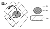
- FIG. 3A is a conceptual diagram of a conventional guest material.
- FIG. 3B is a conceptual diagram of a guest material used for the light-emitting device of one embodiment of the present invention.
- FIG. 4A is a structural formula of a guest material used for the light-emitting device of one embodiment of the present invention.
- FIG. 4B is a ball-and-stick diagram of a guest material used in the light-emitting device of one embodiment of the present invention.
- FIG. 5A is a schematic sectional view of a light emitting layer of a light emitting device of one embodiment of the present invention.
- 5B to 5D are diagrams illustrating the correlation of energy levels of the light emitting layer of the light emitting device of one embodiment of the present invention.
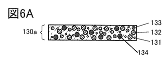
- FIG. 6A is a schematic sectional view of a light emitting layer of a light emitting device of one embodiment of the present invention.
- 6B and 6C are diagrams illustrating the correlation of energy levels of the light emitting layer of the light emitting device of one embodiment of the present invention.
- FIG. 7A is a schematic sectional view of a light emitting layer of a light emitting device of one embodiment of the present invention.
- 7B and 7C are diagrams illustrating the correlation of energy levels of the light emitting layer of the light emitting device of one embodiment of the present invention.
- FIG. 8A is a schematic sectional view of a light emitting layer of a light emitting device of one embodiment of the present invention.
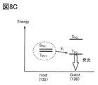
- 8B and 8C are diagrams illustrating the correlation of energy levels of the light emitting layer of the light emitting device of one embodiment of the present invention.
- FIG. 9A is a schematic sectional view of a light emitting layer of a light emitting device of one embodiment of the present invention.
- FIG. 9B and 9C are diagrams illustrating the correlation of energy levels of the light emitting layer of the light emitting device of one embodiment of the present invention.
- FIG. 10A is a schematic sectional view of a light emitting layer of a light emitting device of one embodiment of the present invention.
- 10B and 10C are diagrams illustrating the correlation of energy levels of the light emitting layer of the light emitting device of one embodiment of the present invention.
- FIG. 11A is a schematic sectional view of a light emitting layer of a light emitting device of one embodiment of the present invention.
- FIG. 11B is a diagram illustrating a correlation of energy levels of a light emitting layer of a light emitting device of one embodiment of the present invention.
- FIG. 10A is a schematic sectional view of a light emitting layer of a light emitting device of one embodiment of the present invention.
- FIG. 11B is a diagram illustrating a correlation of energy levels of a light emitting layer of a light emitting device of one embodiment
- FIG. 12 is a schematic cross-sectional view of a light emitting device of one embodiment of the present invention.
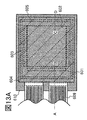
- FIG. 13A is a top view illustrating a display device of one embodiment of the present invention.
- FIG. 13B is a schematic cross-sectional view illustrating the display device of one embodiment of the present invention.
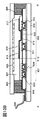
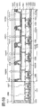
- 14A and 14B are schematic cross-sectional views each illustrating a display device of one embodiment of the present invention.
- 15A and 15B are schematic cross-sectional views each illustrating a display device of one embodiment of the present invention.
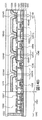
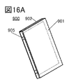
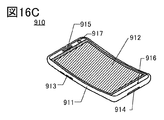
- 16A to 16D are perspective views illustrating a display module of one embodiment of the present invention.
- 17A to 17C are diagrams illustrating electronic devices of one embodiment of the present invention.
- 18A and 18B are perspective views each illustrating a display device of one embodiment of the present invention.
- FIG. 19 is a diagram illustrating a lighting device of one embodiment of the present invention.
- the ordinal numbers given as the first, second, etc. are used for convenience, and may not indicate the process order or the stacking order. Therefore, for example, the description can be made by appropriately replacing “first” with “second” or “third”.
- the ordinal numbers described in this specification and the like may be different from the ordinal numbers used to specify one embodiment of the present invention.
- film and “layer” can be interchanged with each other.
- conductive layer to the term “conductive film”.
- insulating film to the term “insulating layer”.
- a singlet excited state is a singlet state having excitation energy.
- the S1 level is the lowest singlet excitation energy level, and is the lowest singlet excited state (S1 state) excitation energy level.
- a triplet excited state (T * ) is a triplet state having excitation energy.
- the T1 level is the lowest triplet excitation energy level, and is the lowest triplet excited state (T1 state) excitation energy level. Note that in this specification and the like, the S1 state and the S1 level may be expressed even if they are simply described as a singlet excited state and a singlet excited energy level. Further, even when described as a triplet excited state and a triplet excited energy level, it may represent the T1 state and the T1 level.
- the fluorescent material is a compound that emits light in the visible light region when relaxing from the singlet excited state to the ground state.
- a phosphorescent material is a compound that emits light in the visible light region at room temperature when the triplet excited state is relaxed to the ground state.
- the phosphorescent material is one of compounds capable of converting triplet excitation energy into visible light.
- the blue wavelength region is 400 nm or more and less than 490 nm, and blue light emission has at least one emission spectrum peak in the wavelength region.
- the green wavelength region is 490 nm or more and less than 580 nm, and the green emission has at least one emission spectrum peak in the wavelength region.
- the red wavelength region is 580 nm or more and 680 nm or less, and red emission has at least one emission spectrum peak in the wavelength region.
- a light-emitting layer is a layer containing one or more kinds of fluorescent materials or phosphorescent materials.
- the fluorescent light emitting layer is a layer from which light emission having fluorescent light emission is obtained
- the phosphorescent light emitting layer is a layer from which light emission having phosphorescent light emission is obtained.
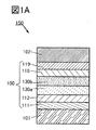
- FIG. 1A and 1B are schematic cross-sectional views of a light emitting device 150 and a light emitting device 152 according to one embodiment of the present invention.
- Each of the light emitting device 150 and the light emitting device 152 has a pair of electrodes (the electrode 101 and the electrode 102) and the EL layer 100 or the EL layer 200 provided between the pair of electrodes.
- the EL layers 100 and 200 each include at least a light emitting layer 130a and a light emitting layer 130b.
- the EL layer 100 illustrated in FIG. 1A has functional layers such as a hole injection layer 111, a hole transport layer 112, an electron transport layer 118, and an electron injection layer 119 in addition to the light emitting layers 130a and 130b.
- the EL layer 200 illustrated in FIG. 1B further includes a separation layer 120. That is, the EL layer 200 has a structure in which the separation layer 120 is added to the EL layer 100.
- the electrode 101 of the pair of electrodes will be described as the anode and the electrode 102 will be described as the cathode, but the configurations of the light emitting device 150 and the light emitting device 152 are not limited thereto. That is, the electrode 101 may be the cathode, the electrode 102 may be the anode, and the layers of the layers between the electrodes may be laminated in the reverse order. That is, the hole injection layer 111, the hole transport layer 112, the light emitting layer 130a, the light emitting layer 130b, the electron transport layer 118, and the electron injection layer 119 may be stacked in this order from the anode side. ..
- the hole transport layer 112 and the light emitting layer 130a are adjacent to each other, and the electron transport layer 118 and the light emitting layer 130b are adjacent to each other, the light emitting device 150 and the light emitting device 152 are configured as follows. Is not the case. That is, in the light emitting device 150 and the light emitting device 152, the hole transport layer 112 and the light emitting layer 130b may be adjacent to each other, and the electron transport layer 118 and the light emitting layer 130a may be adjacent to each other.
- the structures of the EL layer 100 and the EL layer 200 are not limited to those illustrated in FIGS. 1A and 1B, and may be any of the hole injection layer 111, the hole transport layer 112, the electron transport layer 118, and the electron injection layer 119. It suffices to adopt a configuration having at least one selected from Alternatively, the EL layer 100 and the EL layer 200 reduce an injection barrier of holes or electrons, improve transportability of holes or electrons, inhibit transportability of holes or electrons, or have an electrode quenching phenomenon. It may be configured to have a functional layer having a function of suppressing or the like.
- the functional layers may each be a single layer or a structure in which a plurality of layers are laminated.
- the light-emitting layer 130a is described as a fluorescent light-emitting layer containing a fluorescent material
- the light-emitting layer 130b is described as a phosphorescent light-emitting layer containing a phosphorescent material. Therefore, both fluorescence emission and phosphorescence emission can be obtained from the light-emitting device of one embodiment of the present invention.
- the light-emitting device 150 and the light-emitting device 152 of one embodiment of the present invention by applying a voltage between the pair of electrodes (the electrode 101 and the electrode 102), electrons are emitted from the cathode and holes are emitted from the anode, respectively.
- a current flows.
- excitons generated by recombination of carriers electrons and holes
- the ratio of singlet excitons to triplet excitons hereinafter, exciton generation probability
- the proportion of singlet excitons generated is 25% and the proportion of triplet excitons generated is 75%.
- Phosphorescent materials are examples of materials that have the function of converting triplet excitation energy into luminescence.
- a phosphorescent material refers to a compound that exhibits phosphorescence and does not emit fluorescence in any of a temperature range of low temperature (eg, 77 K) to room temperature (ie, 77 K to 313 K). ..
- the phosphorescent material preferably contains a metal element having a large spin-orbit interaction, specifically a transition metal element, particularly a platinum group element (ruthenium (Ru), rhodium (Rh), palladium (Pd), osmium). It is preferable to have (Os), iridium (Ir), or platinum (Pt), and iridium is particularly preferable.
- the presence of Ir can increase the transition probability associated with the direct transition between the singlet ground state and the triplet excited state.
- a TADF material As a material having a function of converting triplet excitation energy into light emission, a TADF material can be mentioned.
- the TADF material is a material having a small difference between the S1 level and the T1 level and capable of converting energy from triplet excitation energy to singlet excitation energy by the intersystem crossing. Therefore, the triplet excitation energy can be up-converted (reverse intersystem crossing) to a singlet excitation energy with a small amount of thermal energy, and a singlet excited state can be efficiently generated.
- an exciplex (also referred to as an exciplex, an exciplex, or an exciplex) that forms an excited state with two kinds of substances has an extremely small difference between the S1 level and the T1 level, and has triplet excitation energy as singlet excitation energy. It has a function as a TADF material that can be converted into.
- a phosphorescence spectrum observed at low temperature may be used as an index of the T1 level.
- a tangent line is drawn at the short wavelength side skirt of the fluorescence spectrum at room temperature or low temperature
- the energy of the wavelength of the extrapolation line is set to the S1 level
- a tangent line is drawn at the short wavelength side skirt of the phosphorescence spectrum.
- the difference between S1 and T1 is preferably 0.2 eV or less.
- a nanostructure of a transition metal compound having a perovskite structure can be mentioned.
- nanostructures of metal halide perovskites are preferable.
- nanoparticles and nanorods are preferable.
- FIG. 2A is a schematic sectional view showing a light emitting layer 130a of a light emitting device which is one embodiment of the present invention.
- the light emitting layer 130a includes the compound 131 and the compound 132.
- the compound 131 has a function of converting triplet excitation energy into light emission
- the compound 132 has a function of converting singlet excitation energy into light emission. Since a fluorescent material has high stability, it is preferable to use a fluorescent material as the compound 132 in order to obtain a highly reliable light emitting device. Since the compound 131 has a function of converting triplet excitation energy into light emission, carrier recombination occurs in the compound 131 in order to obtain a light-emitting device with high emission efficiency.
- both singlet excitation energy and triplet excitation energy of excitons generated by recombination of carriers in the compound 131 finally transfer energy to the singlet excited state of the compound 132 and the compound 132 emits light.
- the compound 131 is an energy donor and the compound 132 is an energy acceptor.
- the light emitting layer 130a is a fluorescent light emitting layer using the compound 131 as a host material and the compound 132 as a guest material. That is, in FIGS. 2A and 2B, the host material has a function as an energy donor and the guest material has a function as an energy acceptor. Further, the light emitting layer 130a can obtain light emission derived from the compound 132 which is a guest material.
- FIG. 2B is an example of energy level correlation in a light emitting layer in a light emitting device of one embodiment of the present invention. This structural example shows the case where a TADF material is used for the compound 131.
- FIG. 2B shows the energy level correlation between the compound 131 and the compound 132 in the light emitting layer 130a.
- the vertical axis of FIG. 2B represents energy (arbitrary unit).
- the notations and symbols in FIG. 2B are as follows.
- the compound 131 has TADF property. Therefore, the compound 131 has a function of converting triplet excitation energy into singlet excitation energy by upconversion (FIG. 2B route A 1 ).
- the singlet excitation energy of the compound 131 can be quickly transferred to the compound 132. (FIG. 2B route A 2 ).
- S C1 ⁇ S G it is preferable that S C1 ⁇ S G.
- a tangent line is drawn at the skirt on the short wavelength side of the fluorescence spectrum of the compound 131, the energy of the wavelength of the extrapolation line is S C1, and the energy of the wavelength of the absorption edge of the absorption spectrum of the compound 132 is S G. In doing so, it is preferable that S C1 ⁇ S G. Since the compound 131 is a material having TADF property, S C1 and T C1 are very small. Therefore, S C1 ⁇ S T1 ⁇ S G.
- the triplet excitation energy generated in the compound 131 transfers energy to the S1 level of the compound 132, which is the guest material, through the routes A 1 and A 2 described above, and the compound 132 emits light, thereby improving the emission efficiency of the fluorescent light emitting device. Can be increased.
- Route A 2 the compound 131 functions as an energy donor and the compound 132 functions as an energy acceptor.
- the compound 131 and the compound 132 are mixed in the light emitting layer 130a. Therefore, a process in which the triplet excitation energy of the compound 131 is converted into the triplet excitation energy of the compound 132 in competition with the routes A 1 and A 2 (FIG. 2B, route A 3 ) may occur. Since the compound 132 is a fluorescent material, the triplet excitation energy of the compound 132 does not contribute to light emission. That is, if the energy transfer of the route A 3 occurs, the luminous efficiency of the light emitting device will decrease. In reality, energy transfer from T C1 to T G (route A 3 ) is not direct, but energy transfer once to a triplet excited state higher than T G of compound 132, and then becomes T G by internal conversion. There may be a route, but the process is omitted in the figure. The subsequent undesired heat deactivation process in the present specification, that is, the deactivation process to TG is all the same.
- the Forster mechanism dipole-dipole interaction
- the Dexter mechanism electron exchange interaction
- the compound 132 which is an energy acceptor
- the Dexter mechanism is dominant in the energy transfer of route A 3 .
- the Dexter mechanism significantly occurs when the distance between the compound 131 which is an energy donor and the compound 132 which is an energy acceptor is 1 nm or less. Therefore, in order to suppress the route A 3 , it is important to increase the distance between the host material and the guest material, that is, the distance between the energy donor and the energy acceptor.
- the concentration of the energy acceptor in the mixed film of these compounds may be lowered.
- the concentration of the energy acceptor in the mixed film is reduced, not only the energy transfer from the energy donor to the energy acceptor based on the Dexter mechanism but also the energy transfer based on the Forster mechanism is suppressed. In that case, since the route A 2 is based on the Forster mechanism, problems such as a decrease in light emitting efficiency and a decrease in reliability of the light emitting device occur.
- the inventors of the present invention can suppress the above-mentioned decrease in luminous efficiency and decrease in reliability by using a fluorescent material having a protective group for increasing the distance from the energy donor as the energy acceptor. I found it. Further, they have found that it is possible to suppress a decrease in the luminous efficiency of the phosphorescent emitting layer which occurs when the phosphorescent emitting layer and the fluorescent emitting layer are combined.
- FIG. 3A shows a conceptual diagram in which a fluorescent material having no protective group, which is a general fluorescent material, is dispersed as a guest material in a host material
- FIG. 3B shows a light emitting device of one embodiment of the present invention.
- the conceptual diagram in the case of using the fluorescent material which has a protective group and is used as a guest material and disperse
- the host material may be read as an energy donor and the guest material may be read as an energy acceptor.
- the protective group has a function of increasing the distance between the luminophore and the host material.
- the guest material 301 has a luminophore 310.
- the guest material 301 has a function as an energy acceptor.
- the guest material 302 has a luminophore 310 and a protective group 320.
- the guest material 301 and the guest material 302 are surrounded by the host material 330. Since the distance between the luminophore and the host material is short in FIG. 3A, energy transfer from the host material 330 to the guest material 301 is performed by energy transfer by the Forster mechanism (route A 4 in FIGS. 3A and 3B) and energy by the Dexter mechanism. Both movement (route A 5 in FIGS. 3A and 3B) can occur.
- the triplet excited state of the guest material is generated by energy transfer of the triplet excited energy from the host material to the guest material by the Dexter mechanism, the triplet excited energy is non-radiatively deactivated when the guest material is a fluorescent material. Therefore, it is one of the causes of the decrease in luminous efficiency.
- the guest material 302 has a protective group 320. Therefore, the distance between the luminescent group 310 and the host material 330 can be increased. Therefore, energy transfer (route A 5 ) by the Dexter mechanism can be suppressed.
- the guest material 302 in order for the guest material 302 to emit light, since the Dexter mechanism is suppressed, the guest material 302 needs to receive energy from the host material 330 by the Forster mechanism. That is, it is preferable to efficiently use the energy transfer by the Forster mechanism while suppressing the energy transfer by the Dexter mechanism. It is known that energy transfer by the Forster mechanism is also affected by the distance between the host material and the guest material. Generally, when the distance between the host material 330 and the guest material 302 is 1 nm or less, the Dexter mechanism is dominant, and when the distance is 1 nm or more and 10 nm or less, the Forster mechanism is dominant.
- the distance between the host material 330 and the guest material 302 is 10 nm or more, energy transfer hardly occurs.
- the distance between the host material 330 and the guest material 302 may be read as the distance between the host material 330 and the light-emitting group 310.
- the protective group 320 extends from the luminophore 310 to a range of 1 nm or more and 10 nm or less. More preferably, it is 1 nm or more and 5 nm or less. With this structure, energy transfer by the Forster mechanism can be efficiently used while suppressing energy transfer from the host material 330 to the guest material 302 by the Dexter mechanism. Therefore, a light emitting device having high luminous efficiency can be manufactured.
- the concentration of the guest material 301 or the guest material 302 with respect to the host material 330.
- the concentration of the guest material is increased, the energy transfer speed of the Dexter mechanism is also increased, and the luminous efficiency is decreased. Therefore, it was difficult to increase the concentration of the guest material.
- a fluorescent light emitting device in which a material having a function of converting triplet excitation energy into light emission is used as a host material, a light emitting device having a low guest material concentration of 1 wt% or less has been reported.
- a guest material having a protective group in a light-emitting group is used for a light-emitting layer. Therefore, the energy transfer by the Forster mechanism can be efficiently used while suppressing the energy transfer by the Dexter mechanism, so that the concentration of the guest material that is the energy acceptor can be increased. As a result, an originally contradictory phenomenon of increasing the energy transfer speed by the Forster mechanism while suppressing the energy transfer by the Dexter mechanism can be enabled. By increasing the energy transfer rate by the Forster mechanism, the excitation lifetime of the energy acceptor in the light emitting layer is shortened, so that the reliability of the light emitting device can be improved.
- the concentration of the guest material is preferably 2 wt% or more and 30 wt% or less with respect to the host material, more preferably 5 wt% or more and 20 wt% or less, and further preferably 5 wt% or more and 15 wt% or less.
- the concentration of the guest material is preferably 2 wt% or more and 30 wt% or less with respect to the host material, more preferably 5 wt% or more and 20 wt% or less, and further preferably 5 wt% or more and 15 wt% or less.
- the light emitting efficiency can be improved by using a fluorescent material having high stability, a light emitting device with favorable reliability can be manufactured.
- the above concentration is a concentration in a case where a material that mainly emits light is a guest material and a material other than the guest material is a host material in the light emitting layer.
- the effect of the light-emitting device of one embodiment of the present invention is not only the effect of improving reliability by using a fluorescent material with high stability.
- the energy transfer as described above always competes with the quenching process due to the influence of deteriorated substances and impurities.
- the rate of light emitted by the light emitting device decreases. That is, the brightness of the light emitting device deteriorates.
- one embodiment of the present invention can suppress energy transfer by the Dexter mechanism and increase the energy transfer speed by the Forster mechanism as compared with a conventional light-emitting device; thus, the influence of competition with the quenching process. Can be made smaller and the life of the device can be extended.
- the luminescent group refers to an atomic group (skeleton) that causes light emission in the fluorescent material.
- the luminophore generally has a ⁇ bond, preferably contains an aromatic ring, and preferably has a condensed aromatic ring or a condensed heteroaromatic ring.
- the luminophore can be regarded as an atomic group (skeleton) including an aromatic ring having a transition dipole vector on the ring plane.
- the skeleton having the lowest S1 level among the plurality of condensed aromatic rings or condensed heteroaromatic rings is used as the fluorescent material.
- the skeleton having the absorption edge at the longest wavelength may be considered as the luminescent group of the fluorescent material.
- the luminophore of the fluorescent material can be predicted from the shape of the emission spectrum of each of the plurality of condensed aromatic rings or the condensed heteroaromatic rings.
- Examples of the condensed aromatic ring or the condensed heteroaromatic ring include a phenanthrene skeleton, a stilbene skeleton, an acridone skeleton, a phenoxazine skeleton, and a phenothiazine skeleton.
- a fluorescent material having a naphthalene skeleton, anthracene skeleton, fluorene skeleton, chrysene skeleton, triphenylene skeleton, tetracene skeleton, pyrene skeleton, perylene skeleton, coumarin skeleton, quinacridone skeleton, and naphthobisbenzofuran skeleton is preferable because of high fluorescence quantum yield.
- the substituent used as the protective group needs to have a triplet excitation energy level higher than the T1 level of the luminophore and the host material. Therefore, it is preferable to use a saturated hydrocarbon group. This is because the substituent having no ⁇ bond has a high triplet excitation energy level. Further, a substituent having no ⁇ bond has a low function of transporting carriers (electrons or holes). Therefore, the saturated hydrocarbon group can increase the distance between the luminophore and the host material without affecting the excited state of the host material or the carrier transport property.
- the frontier orbital ⁇ HOMO Highest Occupied Molecular Orbital, and the highest occupied molecular orbital are present
- LUMO Large Unoccupied Molecular Orbital, also referred to as the lowest unoccupied orbit
- the luminophore often has a frontier orbit.
- overlapping of HOMO of energy donor and energy acceptor and overlapping of LUMO are important.
- the distance between the frontier orbital of the host material, which is the energy donor, and the frontier orbital of the guest material, which is the energy acceptor, can be increased, and energy transfer by the Dexter mechanism can be achieved. Can be suppressed.
- the protective group examples include an alkyl group having 1 to 10 carbon atoms. Further, since the protective group needs to increase the distance between the luminophore and the host material, a bulky substituent is preferable. Therefore, an alkyl group having 3 to 10 carbon atoms, a substituted or unsubstituted cycloalkyl group having 3 to 10 carbon atoms, or a trialkylsilyl group having 3 to 12 carbon atoms can be preferably used. Particularly, as the alkyl group, a bulky branched chain alkyl group is preferable. Further, it is particularly preferable that the substituent has a quaternary carbon because it becomes a bulky substituent.
- one luminophore has five or more protecting groups.
- the entire luminophore can be covered with the protective group, so that the distance between the host material and the luminophore can be appropriately adjusted.
- FIG. 3B shows a state in which the luminophore and the protective group are directly bonded, but it is more preferable that the protective group is not directly bonded to the luminophore.
- the protecting group may be bonded to the luminophore through a divalent or higher valent substituent such as an arylene group or an amino group.
- the protective group is bonded to the luminophore through the substituent, the distance between the luminophore and the host material can be effectively increased. Therefore, when the luminophore and the protecting group are not directly bonded, if four or more protecting groups are provided for one luminophore, the energy transfer due to the Dexter mechanism can be effectively suppressed.
- the divalent or higher valent substituent that connects the luminescent group and the protective group is preferably a substituent having a ⁇ -conjugated system. With such a structure, physical properties such as an emission color of the guest material, a HOMO level, and a glass transition point can be adjusted.
- the protective group is preferably arranged on the outermost side when the molecular structure is centered around the luminophore.
- N,N′-[(2-tert-butylanthracene)-9,10- which is a fluorescent material represented by the following structural formula (102) and can be used for the light-emitting device of one embodiment of the present invention.
- the structure of diyl]-N,N'-bis(3,5-di-tert-butylphenyl)amine (abbreviation: 2tBu-mmtBuDPhA2Anth) is shown.
- 2tBu-mmtBuDPhA2Anth the anthracene ring is a luminescent group, and the tertiary butyl (tBu) group acts as a protective group.
- FIG. 4B shows a state when 2tBu-mmtBuDPhA2Anth is viewed from the direction of the arrow in FIG. 4A (horizontal direction with respect to the anthracene ring surface).
- the shaded portion in FIG. 4B represents the portion directly above the anthracene ring surface that is the luminescent group, and it can be seen that there is a region where the tBu group, which is a protecting group, overlaps with the portion directly above this.
- the atom indicated by the arrow (a) is a carbon atom of the tBu group overlapping with the shaded portion
- the atom indicated by the arrow (b) is a hydrogen atom of the tBu group overlapping with the shaded portion.
- the distance between the anthracene ring and the host material can be increased in both the plane direction and the vertical direction of the anthracene ring that is the luminescent group, Energy transfer due to the Dexter mechanism can be suppressed.
- the Dexter mechanism significantly occurs when the HOMO and LUMO of both materials overlap. Therefore, in order to suppress the Dexter mechanism, it is important to suppress the overlap of HOMO and LUMO of both materials. That is, it is important to increase the distance between the skeleton related to the excited state and the host material.
- the luminophore often has both HOMO and LUMO.
- the HOMO and LUMO of the guest material are spread above and below the surface of the luminophore (in the case of 2tBu-mmtBuDPhA2Anth, above and below the anthracene ring), they cover the above and below the surface of the luminophore with protective groups. Is important in the molecular structure.
- the upper side and the lower side of the anthracene ring represent the upper side and the lower side with the anthracene ring surface as the reference plane when viewed from the arrow in FIG. 4A.
- a protective group such as a tBu group is arranged so as to cover a luminescent group such as an anthracene ring.
- FIG. 5C is an example of a correlation of energy levels in the light emitting layer 130a of the light emitting device 150 and the light emitting device 152 according to one embodiment of the present invention.
- the light-emitting layer 130a illustrated in FIG. 5A includes the compound 131, the compound 132, and the compound 133.
- compound 132 is preferably a fluorescent material.
- the compound 131 and the compound 133 are a combination that forms an exciplex.
- the combination of the compound 131 and the compound 133 may be a combination capable of forming an exciplex, but one is a compound having a function of transporting holes (hole transporting property) and the other is a compound of electrons.
- a compound having a transporting function is more preferable.
- a donor-acceptor type exciplex can be easily formed, and an exciplex can be efficiently formed.
- the carrier balance can be easily controlled by the mixing ratio.
- the range of compound having hole transporting property: compound having electron transporting property 1:9 to 9:1 (weight ratio) is preferable.
- the carrier balance can be easily controlled by having the structure, the carrier recombination region can be easily controlled.
- one of the compound 131 and the compound 133 has a higher HOMO level than the other HOMO level, and one LUMO level higher than the other LUMO level. It is preferable.
- the HOMO level of the compound 131 may be equivalent to the HOMO level of the compound 133, or the LUMO level of the compound 131 may be equivalent to the LUMO level of the compound 133.
- the LUMO level and HOMO level of a compound can be derived from the electrochemical characteristics (reduction potential and oxidation potential) of the compound measured by cyclic voltammetry (CV) measurement.
- the HOMO level of the compound 131 is higher than the HOMO level of the compound 133 as shown in the energy band diagram in FIG. 5B.
- the LUMO level of the compound 131 is preferably higher than the LUMO level of the compound 133.
- Comp(131) represents the compound 131
- Comp(133) represents the compound 133
- ⁇ E C1 represents the energy difference between the LUMO level and the HOMO level of the compound 131
- ⁇ E C3 represents the compound.
- 133 represents the energy difference between the LUMO level and the HOMO level of 133
- ⁇ E E is a notation and code indicating the energy difference between the LUMO level of the compound 131 and the HOMO level of the compound 133.
- the excitation energy of the exciplex approximately corresponds to the energy difference ( ⁇ E E ) between the LUMO level of the compound 133 and the HOMO level of the compound 131, and the energy difference between the LUMO level and the HOMO level of the compound 131. ( ⁇ E C1 ) and the energy difference ( ⁇ E C3 ) between the LUMO level and the HOMO level of Compound 133. Therefore, by forming an exciplex with the compound 131 and the compound 133, it becomes possible to form an excited state with lower excitation energy. Further, since it has a lower excitation energy, the exciplex can form a stable excited state.
- FIG. 5C shows the correlation of the energy levels of the compound 131, the compound 132, and the compound 133 in the light emitting layer 130a.
- -Comp(131) Compound 131
- -Comp(133) Compound 133 ⁇ Guest (132): Compound 132
- S C1 S1 level of compound 131.
- T C1 T1 level of compound 131.
- S C3 S1 level of compound 133.
- T C3 S1 level of compound 133.
- T G T1 level of compound 132.
- the compound 131 and the compound 133 included in the light-emitting layer 130a form an exciplex.
- the S1 level (S E ) of the exciplex and the T1 level (T E ) of the exciplex are energy levels adjacent to each other (see route A 6 in FIG. 5C).
- the excitation energy levels (S E and T E ) of the exciplex are lower than the S1 levels (S C1 and S C3 ) of the substances (compound 131 and compound 133) forming the exciplex, lower excitation energy is obtained.
- the excited state can be formed by. Accordingly, the driving voltage of the light-emitting device of one embodiment of the present invention can be reduced.
- the exciplex Since the S1 level (S E ) and the T1 level (T E ) of the exciplex are energy levels adjacent to each other, the inter-reciprocal intersections easily occur and TADF property is exhibited. Therefore, the exciplex has a function of converting triplet excitation energy into singlet excitation energy by upconversion (FIG. 5C, route A 7 ). The singlet excitation energy of the exciplex can quickly move to the compound 132. ( Figure 5C route A 8). At this time, it is preferable that S E ⁇ S G. In Route A 8 , the exciplex is the energy donor and compound 132 functions as the energy acceptor.
- a tangent line is drawn at the short wavelength side skirt of the fluorescence spectrum of the exciplex, the energy of the wavelength of the extrapolation line is S E, and the energy of the wavelength of the absorption edge of the absorption spectrum of the compound 132 is S G. In doing so, it is preferable that S E ⁇ S G.
- the T1 levels of both the compound 131 and the compound 133 are equal to or higher than T E.
- the index it is preferable that the shortest emission peak wavelengths of the phosphorescence spectra of the compound 131 and the compound 133 are both less than or equal to the maximum emission peak wavelength of the exciplex.
- a tangent line is drawn at the short wavelength side skirt of the fluorescence spectrum of the exciplex, the energy of the wavelength of the extrapolation line is S E, and a tangent line is drawn at the short wavelength side skirt of the compound 131 and compound 133, respectively.
- S E ⁇ T C1 ⁇ 0.2 eV and S E ⁇ T C3 ⁇ 0.2 eV when the energy of the wavelength of the extrapolated line is T C1 and T C3 of each compound. ..
- the guest material emits light by the triplet excitation energy generated in the light emitting layer 130a passing through energy transfer (route A 8 ) from the S1 level of the above-mentioned route A 6 and exciplex to the S1 level of the guest material. be able to. Therefore, by using a combination of materials that form an exciplex in the light emitting layer 130a, it is possible to increase the light emission efficiency of the fluorescent light emitting device.
- a guest material having a protective group in a light-emitting group is used for the compound 132.
- energy transfer by the Dexter mechanism represented by route A 9 can be suppressed, and deactivation of triplet excitation energy can be suppressed. Therefore, a fluorescent light emitting device device having high luminous efficiency can be obtained.
- the processes of the routes A 6 to A 8 described above may be referred to as “Exset-Singlet Energy Transfer” or “ExEF (Enhanced-Enhanced Fluorescence)”.
- ExEF Enhanced-Enhanced Fluorescence
- the light emitting layer 130a has donation of excitation energy from the exciplex to the fluorescent material.
- a compound having a heavy atom is used as one of the compounds forming the exciplex. Therefore, intersystem crossing between the singlet state and the triplet state is promoted. Therefore, an exciplex capable of transition from the triplet excited state to the singlet ground state (that is, capable of exhibiting phosphorescence) can be formed.
- the triplet excitation energy level (T E ) of the exciplex becomes an energy donor level, so that T E is a singlet excitation energy level of the compound 132 which is a light-emitting material. It is preferably at least (S G ).
- a tangent line is drawn at the short-wavelength side skirt of the emission spectrum of an exciplex in which one compound has a heavy atom, and the energy of the wavelength of the extrapolation line is set to T E, and the absorption of the compound 132 is absorbed.
- T E the energy of the wavelength of the absorption edge of the spectrum upon the S G.
- S G compound 132 from the triplet excited energy level of the exciplex (T E) Energy can be transferred to.
- S1 quasi-position of the exciplex (S E) and the T1 level position (T E) are the energy levels adjacent to each other, in an emission spectrum, when it is difficult to clearly distinguish between fluorescence and phosphorescence There is. In that case, it may be possible to distinguish between fluorescence and phosphorescence depending on the emission lifetime.
- the phosphorescent material used in the above structure preferably contains a heavy atom such as Ir, Pt, Os, Ru, or Pd.
- the quantum yield may be high or low. That is, the energy transfer from the triplet excitation energy level of the exciplex to the singlet excitation energy level of the guest material may be allowed transition.
- the energy transfer from the exciplex composed of the phosphorescent material or the phosphorescent material to the guest material as described above is performed from the triplet excitation energy level of the energy donor to the singlet excitation energy level of the guest material (energy acceptor). Is preferable because the energy transfer to is an allowable transition.
- the triplet excitation energy of the exciplex can be transferred to the S1 level (S G ) of the guest material by the process of route A 8 without passing through the process of route A 7 in FIG. 5C. That is, the triplet and singlet excitation energies can be transferred to the S1 level of the guest material only in the processes of route A 6 and route A 8 .
- the exciplex is the energy donor and compound 132 functions as the energy acceptor.
- a guest material having a protective group in a light-emitting group is used for the compound 132.
- energy transfer by the Dexter mechanism represented by route A 9 can be suppressed, and deactivation of triplet excitation energy can be suppressed. Therefore, a fluorescent light emitting device with high luminous efficiency can be obtained.
- the compound 133 Since the compound 133 is a TADF material, the compound 133 that does not form an exciplex has a function of converting triplet excitation energy into singlet excitation energy by upconversion (FIG. 5D route A 10 ). The singlet excitation energy of the compound 133 can quickly move to the compound 132. (FIG. 5D Route A 11 ). At this time, it is preferable that S C3 ⁇ S G.
- a route in which triplet excitation energy moves to the compound 132 which is a guest material through the route A 6 to the route A 8 in FIG. 5D. Then, there is a route to move to the compound 132 via route A 10 and route A 11 in FIG. 5D. Since there are multiple paths through which the triplet excitation energy moves to the fluorescent material, the light emission efficiency can be further increased.
- the exciplex is the energy donor and compound 132 functions as the energy acceptor.
- compound 133 is an energy donor and compound 132 functions as an energy acceptor.
- the exciplex and the compound 133 are energy donors, and the compound 132 functions as an energy acceptor.
- FIG. 6A shows the case where four kinds of materials are used for the light emitting layer 130a.
- the light emitting layer 130a includes a compound 131, a compound 132, a compound 133, and a compound 134.
- the compound 133 has a function of converting triplet excitation energy into light emission.
- the compound 133 is a phosphorescent compound will be described.
- the compound 132 is a guest material that exhibits fluorescence emission.
- the compound 131 is an organic compound that forms an exciplex with the compound 134.
- FIG. 6B shows the correlation of energy levels of the compound 131, the compound 132, the compound 133, and the compound 134 in the light emitting layer 130a.
- the notations and symbols in FIG. 6B are as follows, and the other notations and symbols are the same as the notations and symbols shown in FIG. 5C.
- S C4 S1 level of compound 134
- T C4 T1 level of compound 134
- the compound 131 and the compound 134 included in the light-emitting layer 130a form an exciplex.
- the exciplex formed in the above process loses its excitation energy, and the two kinds of substances that formed the exciplex behave as the original separate substances.
- the excitation energy levels (S E and T E ) of the exciplex are lower than the S1 levels (S C1 and S C4 ) of the substances (compound 131 and compound 134) forming the exciplex, the excitation energy is lower. It is possible to form an excited state with. Thereby, the drive voltage of the light emitting device 150 and the light emitting device 152 can be reduced.
- the compound 133 when the compound 133 is a phosphorescent material, the intersystem crossing between the singlet state and the triplet state is allowed. Therefore, both the singlet excitation energy and the triplet excitation energy of the exciplex rapidly move to the compound 133 (route A 13 ). At this time, it is preferable that T E ⁇ T C3 . Further, the triplet excitation energy of the compound 133 can be efficiently converted into the singlet excitation energy of the compound 132 (route A 14 ).
- T E ⁇ T C3 ⁇ S G is preferable because the excitation energy of the compound 133 is efficiently transferred to the compound 132 which is a guest material as singlet excitation energy.
- a tangent line is drawn at the short wavelength side skirt of the phosphorescence spectrum of the compound 133, the energy of the wavelength of the extrapolation line is T C3, and the energy of the wavelength of the absorption edge of the absorption spectrum of the compound 132 is S G. In doing so, it is preferable that T C3 ⁇ S G.
- compound 133 functions as an energy donor and compound 132 functions as an energy acceptor.
- the combination of the compound 131 and the compound 134 may be a combination capable of forming an exciplex, but one is a compound having a hole transporting property and the other is a compound having an electron transporting property. More preferably.
- the HOMO level of the compound 131 is higher than the HOMO level of the compound 134 and the LUMO level of the compound 131 is higher than the LUMO level of the compound 134, or the HOMO level of the compound 134 is HOMO of the compound 131. It is preferable that the combination is higher than the level and the LUMO level of the compound 134 is higher than the LUMO level of the compound 131 because an exciplex can be efficiently formed.
- the correlation of the energy levels of the compound 131 and the compound 134 is not limited to FIG. 6B. That is, the singlet excitation energy level (S C1 ) of the compound 131 may be higher or lower than the singlet excitation energy level (S C4 ) of the compound 134. In addition, the triplet excitation energy level (T C1 ) of the compound 131 may be higher or lower than the triplet excitation energy level (T C4 ) of the compound 134.
- the compound 131 preferably has a ⁇ -electron deficient skeleton. With such a structure, the LUMO level of the compound 131 is lowered, which is suitable for formation of an exciplex.
- the compound 131 preferably has a ⁇ -electron excess skeleton. With such a structure, the HOMO level of the compound 131 is increased, which is suitable for formation of an exciplex.
- a guest material having a protective group in a light-emitting group is used for the compound 132.
- energy transfer by the Dexter mechanism represented by route A 15 can be suppressed, and deactivation of triplet excitation energy can be suppressed. Therefore, a fluorescent light emitting device with high luminous efficiency can be obtained.
- concentration of the compound 133 which is an energy donor can be increased. As a result, an originally contradictory phenomenon of increasing the energy transfer speed by the Forster mechanism while suppressing the energy transfer by the Dexter mechanism can be enabled.
- the concentration thereof is preferably 2 wt% or more and 50 wt% or less, more preferably 5 wt% or more and 30 wt% or less, and further preferably 5 wt% or more and 20 wt% with respect to the host material. % Or less.
- the processes of the routes A 12 and A 13 described above may be referred to as ExTET (Exciplex-Triple Energy Transfer) in this specification and the like.
- the light emitting layer 130a has the donation of the excitation energy from the exciplex to the compound 133. Therefore, the present configuration example can be said to be a configuration in which a fluorescent material having a protective group is mixed with a light emitting layer that can use ExTET.
- FIG. 6C shows the case where four kinds of materials are used for the light emitting layer 130a.
- the light emitting layer 130a includes a compound 131, a compound 132, a compound 133, and a compound 134.
- the compound 133 has a function of converting triplet excitation energy into light emission.
- the compound 132 is a guest material that exhibits fluorescence emission.
- the compound 131 is an organic compound that forms an exciplex with the compound 134.
- the compound 134 since the compound 134 is a TADF material, the compound 134 that does not form an exciplex has a function of converting triplet excitation energy into singlet excitation energy by up-conversion (route A 16 in FIG. 6C ). The singlet excitation energy possessed by the compound 134 can be rapidly transferred to the compound 132. (FIG. 6C Route A 17 ).
- S C4 ⁇ S G.
- a tangent line is drawn at the short wavelength side skirt of the fluorescence spectrum of the compound 134, the energy of the wavelength of the extrapolation line is S C4, and the energy of the wavelength of the absorption edge of the absorption spectrum of the compound 132 is S G. In doing so, it is preferable that S C4 ⁇ S G.
- a route in which triplet excitation energy moves to the compound 132 which is a guest material through the route A 12 to the route A 14 in FIG. 6B. Then, there is a route to move to the compound 132 via route A 16 and route A 17 in FIG. 6C. Since there are multiple paths through which the triplet excitation energy moves to the fluorescent material, the light emission efficiency can be further increased.
- compound 133 functions as an energy donor and compound 132 functions as an energy acceptor.
- the compound 134 functions as an energy donor and the compound 132 functions as an energy acceptor.
- FIG. 7B illustrates an example of energy level correlation in the light-emitting layer 130a of the light-emitting device 150 and the light-emitting device 152 of one embodiment of the present invention.
- the light emitting layer 130a illustrated in FIG. 7A includes the compound 131, the compound 132, and the compound 133.
- compound 132 is a fluorescent material having a protecting group.
- the compound 133 has a function of converting triplet excitation energy into light emission. In this structural example, the case where the compound 133 is a phosphorescent material will be described.
- singlet excitons and triplet excitons are generated mainly by carrier recombination in the compound 131 included in the light-emitting layer 130a.
- the compound 133 is a phosphorescent material
- both singlet and triplet excitation energies generated in the compound 131 are transferred to the T C3 level of the compound 133. This can be done (Fig. 7B route A 18 ). Note that some carriers can be recombined with the compound 133.
- the phosphorescent material used in the above structure preferably contains a heavy atom such as Ir, Pt, Os, Ru, or Pd.
- the phosphorescent material acts as an energy donor, so that the quantum yield may be high or low.
- energy transfer from the triplet excitation energy level of the energy donor to the singlet excitation energy level of the guest material (energy acceptor) is an allowable transition, which is preferable. Therefore, the triplet excitation energy of the compound 133 can be transferred to the S1 level (S G ) of the guest material by the process of Route A 19 .
- compound 133 functions as an energy donor and compound 132 functions as an energy acceptor.
- T C3 ⁇ S G because the excitation energy of the compound 133 is efficiently transferred to the singlet excited state of the compound 132 which is a guest material.
- a tangent line is drawn at the short wavelength side skirt of the phosphorescence spectrum of the compound 133, the energy of the wavelength of the extrapolation line is T C3, and the energy of the wavelength of the absorption edge of the absorption spectrum of the compound 132 is S G. In doing so, it is preferable that T C3 ⁇ S G.
- a guest material having a protective group in a light-emitting group is used for the compound 132.
- energy transfer by the Dexter mechanism represented by the route A 20 can be suppressed, and deactivation of triplet excitation energy can be suppressed. Therefore, a fluorescent light emitting device with high luminous efficiency can be obtained.
- FIG. 7C is an example of a correlation of energy levels in the light-emitting device 150 and the light-emitting layer 130a of the light-emitting device of one embodiment of the present invention.
- the light emitting layer 130a illustrated in FIG. 7A includes the compound 131, the compound 132, and the compound 133.
- compound 132 is a fluorescent material having a protecting group.
- the compound 133 has a function of converting triplet excitation energy into light emission. In this structural example, the case where the compound 133 is a compound having a TADF property will be described.
- singlet excitons and triplet excitons are generated mainly by carrier recombination in the compound 131 included in the light-emitting layer 130a.
- a material having a relationship of S C3 ⁇ S C1 and T C3 ⁇ T C1 here, both the singlet excitation energy and the triplet excitation energy generated in the compound 131 are transferred to the S C3 and T C3 levels of the compound 133. It can be moved (Fig. 7C Route A 21 ). Note that some carriers can be recombined with the compound 133.
- compound 133 is a TADF material, it has a function of converting triplet excitation energy into singlet excitation energy by up-conversion (FIG. 7C, route A 22 ). Further, the singlet excitation energy of the compound 133 can be quickly transferred to the compound 132. ( Figure 7C route A 23).
- S C3 ⁇ S G it is preferable that S C3 ⁇ S G. Specifically, a tangent line is drawn on the short wavelength side skirt of the fluorescence spectrum of the compound 133, the energy of the wavelength of the extrapolation line is S C3, and the energy of the wavelength of the absorption edge of the absorption spectrum of the compound 132 is S G. In doing so, it is preferable that S C3 ⁇ S G.
- the triplet excitation energy in the light emitting layer 130a can be converted into the fluorescence emission of the compound 132.
- the compound 133 functions as an energy donor and the compound 132 functions as an energy acceptor.
- a guest material having a protective group in a light-emitting group is used for the compound 132.
- energy transfer by the Dexter mechanism represented by route A 24 can be suppressed, and deactivation of triplet excitation energy can be suppressed. Therefore, a fluorescent light emitting device with high luminous efficiency can be obtained.
- FIG. 8B is an example of a correlation of energy levels in the light emitting layer 130b of the light emitting device 150 and the light emitting device 152 according to one embodiment of the present invention.
- the light emitting layer 130b illustrated in FIGS. 8A, 8B, and 8C includes at least the compound 135 and the compound 136.
- the compound 136 has a function of converting triplet excitation energy into light emission.
- compound 136 is preferably a phosphorescent material.
- 8A, 8B, and 8C show the case where the compound 136 is a phosphorescent material in this structural example.
- FIGS. 8B and 8C The notations and symbols in FIGS. 8B and 8C are as follows.
- singlet excitons and triplet excitons are generated mainly by recombination of carriers in the compound 135 included in the light-emitting layer 130b.
- the compound 136 is a phosphorescent material
- both singlet and triplet excitation energies generated in the compound 135 are transferred to the T PG1 level of the compound 136.
- Can be done (FIGS. 8B and 8C route E 1 ). Note that some carriers can be recombined with the compound 136.
- the absorption band of the longest wavelength in the absorption spectrum of the compound 136 overlaps with the emission spectrum of the compound 135.
- the longest wavelength absorption band of the phosphorescent material is the absorption band that contributes to the strongest emission in the absorption bands included in the entire absorption spectrum.
- examples of the emission spectrum of the compound 135 include a fluorescence spectrum which is light emission derived from a singlet excited state of the compound and a phosphorescence spectrum which is derived from a triplet excited state of the compound.
- both the fluorescence spectrum and the phosphorescence spectrum of the compound 135 overlap with the absorption band of the compound 136 having the longest wavelength.
- the excitation energy of the compound 135 is converted into the excitation energy of the compound 136.
- the energy value of the fluorescence spectrum peak of the compound 135 and the peak of the absorption band of the longest wavelength (low energy side) of the absorption spectrum is preferably 0.2 eV or less. More preferably, it is 0.1 eV or less. With such a structure, a light-emitting layer with high emission efficiency can be obtained.
- the magnitude relationship between the peak energy value of the fluorescence spectrum and the peak value of the absorption band at the longest wavelength (low energy side) of the absorption spectrum does not matter. That is, the energy value of the peak of the fluorescence spectrum may be larger or smaller than the peak value of the absorption band at the longest wavelength (low energy side) of the absorption spectrum.
- the driving voltage of the light emitting device can be reduced while having high light emission efficiency.
- the material having a small energy difference between the S1 level and the T1 level include a TADF material and an exciplex.
- ⁇ Structure Example 2 of Light-Emitting Layer 130b> 9B and 9C are examples of energy level correlations in the light-emitting layer 130b of the light-emitting device 150 and the light-emitting device 152 of one embodiment of the present invention.
- the light-emitting layer 130b illustrated in FIGS. 9A, 9B, and 9C includes at least the compound 135_1, the compound 135_2, and the compound 136.
- the compound 136 has a function of converting triplet excitation energy into light emission.
- compound 136 is preferably a phosphorescent material.
- 9A, 9B, and 9C show the case where the compound 136 is a phosphorescent material in this structural example.
- the compound 135_1 and the compound 135_2 are a combination that forms an exciplex.
- the combination of the compound 135_1 and the compound 135_2 may be a combination capable of forming an exciplex, but one has a function of transporting holes ( More preferably, it is a compound having a hole transporting property, and the other is a compound having a function of transporting an electron (electron transporting property).
- 9B is different from that of FIG. 5B in the reference numerals of the compounds, and the other configurations are the same, and the configurations of the compound 135_1 and the compound 135_2 are the same as the configurations of the compound 131 and the compound 133 in FIG. 5B. Therefore, detailed description of FIG. 9B is omitted.
- Comp(135_1) represents the compound 135_1
- Comp(135_2) represents the compound 135_2
- ⁇ E PH2 represents the energy difference between the LUMO level and the HOMO level of the compound 135_1
- ⁇ E PH3 is the compound.
- 135_2 represents the energy difference between the LUMO level and HOMO level of 135_2
- ⁇ E PH1 is a notation and code indicating the energy difference between the LUMO level of compound 135_1 and the HOMO level of compound 135_2.
- -Host (135_1) Compound 135_1 ⁇ Host (135_2): Compound 135_2 ⁇ Guest (136): Compound 136 • S PH2 : S1 level of compound 135_1 • T PH2 : T1 level of compound 135_1 • S PH3 : S1 level of compound 135_2 • T PH3 : T1 level of compound 135_2 • T PG : T1 level of compound 136 -SPG : S1 level of compound 136- SPE : S1 level of exciplex- TPE : T1 level of exciplex
- One of Compound 135_1 and Compound 135_2 rapidly forms an exciplex by receiving a hole in one and the electron in the other (see Route E 2 in FIG. 9C).
- it when one is in an excited state, it rapidly interacts with the other to form an exciplex.
- the excitation energy level (S PE or T PE ) of the exciplex is lower than the S1 level (S PH1 and S PH2 ) of the host material (compound 135_1 and compound 135_2) forming the exciplex, the excitation energy is lower.
- the drive voltage of the light emitting device can be reduced.
- ExTET The process of the routes E 1 to E 4 described above may be referred to as ExTET in this specification and the like.
- the light emitting layer 130b has the donation of excitation energy from the exciplex to the compound 136. Therefore, in this configuration example, ExTET is applied to the light emitting layer 130b.
- the absorption band of the longest wavelength in the absorption spectrum of the compound 136 overlaps with the emission spectrum of the exciplex. It is known that the S1 level and the T1 level of the exciplex are close to each other. Therefore, at least one of the fluorescence spectrum and the phosphorescence spectrum of the exciplex overlaps with the absorption band of the longest wavelength of the compound 136, so that both the singlet excitation energy and the triplet excitation energy generated in the light-emitting layer 130b can be efficiently compounded. It can be converted into light emission of 136.
- the energy value of the peak of the fluorescence spectrum of the exciplex and the longest wavelength (low energy side) of the absorption spectrum of The difference from the peak value of the absorption band is preferably 0.2 eV or less. More preferably, it is 0.1 eV or less. With such a structure, a phosphorescent light emitting layer with high emission efficiency can be obtained.
- the magnitude relationship between the peak energy value of the fluorescence spectrum of the exciplex and the peak value of the absorption band at the longest wavelength (low energy side) of the absorption spectrum of the compound 136 does not matter. That is, the peak energy value of the fluorescence spectrum of the exciplex may be larger or smaller than the peak value of the absorption band at the longest wavelength (low energy side) of the absorption spectrum of the compound 136.
- the light-emitting device of one embodiment of the present invention includes both the light-emitting layer 130a and the light-emitting layer 130b described above.
- FIG. 10B is an example of a correlation of energy levels in the light-emitting layers 130a and 130b of the light-emitting device 150 and the light-emitting device 152 of one embodiment of the present invention.
- FIG. 10A illustrates a state in which the light emitting layer 130a and the light emitting layer 130b are brought close to each other, and the light emitting layer 130a includes a compound 131_f and a compound 132_f.
- the light-emitting layer 130b includes the compound 135_p and the compound 136_p.
- the compound 132_f is a fluorescent material having a protective group.
- the compound 131_f has a function of converting triplet excitation energy into light emission.
- the compound 131_f is a material having a TADF property and the compound 136_p is a phosphorescent material will be described. That is, in this configuration example, the configuration shown in the configuration example 1 of the light emitting layer 130a as the light emitting layer 130a and the configuration shown in the configuration example 1 of the light emitting layer 130b as the light emitting layer 130b are applied.
- the energy transfer of the routes A 1 to A 3 and the route E 1 is as described above.
- the light emitting layer 130a and the light emitting layer 130b are close to each other.
- the triplet excitation energy generated in the phosphorescent light emitting layer causes the host material (see route Q 1 in FIG. 10B) or the guest material (route 10 in FIG. 10B) included in the fluorescent light emitting layer. move to Q reference 2), resulting in deactivation. That is, there is a problem that the luminous efficiency is lowered when the fluorescent light emitting layer and the phosphorescent light emitting layer are brought close to each other.
- the triplet excited state has a long relaxation time and thus the exciton has a long diffusion distance, and even if it is an exciton generated inside the light emitting layer separated from the fluorescence emitting layer, the exciton moves to the fluorescence emitting layer, It may be deactivated.
- a compound having a function of converting triplet excitation energy into light emission is used in order to transfer the triplet excitation energy generated in the light-emitting layer 130a to the compound 132_f.
- 10B and 10C show an example in which a material having a TADF property is used as the compound 131_f.
- FIG. 10B shows the case where a compound satisfying T FH ⁇ T PH is further used as the compound 135_p.
- the triplet excitation energy transferred to T FH by the route Q 1 which has been a problem until now is converted into fluorescence emission via the route A 1 and the route A 2 . That is, the route Q 1 does not become a deactivation route.
- the triplet excited energy transferred to the T FH similarly by the root Q 1 even when using a phosphorescent compound to compound 131_f is converted into fluorescence (see FIG. 7B route A 19).
- the singlet and triplet excitation energies generated in the light emitting layer 130b which is a phosphorescent light emitting layer are also converted into phosphorescent light emission via the route E 1 .
- a fluorescent material having a protective group is used as the compound 132_f. Therefore, triplet excitation energy transfer from the compound 131_f by the Dexter mechanism can be suppressed. Similarly, triplet excitation energy transfer from the phosphorescent host material to the fluorescent guest material, which is shown in Route Q 2 , is also suppressed because it is energy transfer by the Dexter mechanism.
- the triplet excitation energy of the phosphorescent light emitting layer can be suppressed even though the fluorescent light emitting layer and the phosphorescent light emitting layer are close to each other. Therefore, both fluorescence emission and phosphorescence emission can be efficiently obtained.
- the ratio of fluorescent emission to phosphorescent emission can be changed by adjusting the light emitting region in the light emitting device. Therefore, it is possible to finely adjust the emission color by using a material in which the fluorescent material and the phosphorescent material exhibit different emission colors.
- T FH ⁇ T PG when T FH ⁇ T PG , the triplet excitation energy of the compound 136 — p is transferred to the compound 131 — f, so that the triplet excitation energy is not deactivated but phosphorescence emission is difficult to be obtained. Therefore, in one embodiment of the present invention, T PG ⁇ T FH is preferable.
- the structure of S FG ⁇ T FH is preferable as described above. That is, it is preferable that T PG ⁇ S FG ⁇ T FH .
- the emission color of the fluorescent material is preferably shorter than the emission color of the phosphorescent material.
- the peak wavelength of the emission spectrum of the fluorescent material is preferably shorter than the peak wavelength of the phosphorescent material.
- FIG. 11B illustrates an example of energy level correlation in the light-emitting layers 130a and 130b of the light-emitting device 150 and the light-emitting device 152 of one embodiment of the present invention.
- FIG. 11A illustrates a state in which the light emitting layer 130a and the light emitting layer 130b are brought close to each other, and the light emitting layer 130a includes a compound 131_f and a compound 132_f.
- the light-emitting layer 130b includes the compound 135_p and the compound 136_p, and the compound 135_p includes the compound 135_1p and the compound 135_2p.
- the compound 132_f is a fluorescent material having a protective group.
- the compound 131_f has a function of converting triplet excitation energy into light emission.
- the compound 131_f is a material having a TADF property
- the compound 136_p is a phosphorescent material
- the compounds 135_1p and 135_2p are a combination forming an exciplex. That is, in the present configuration example, the configuration shown in the configuration example 1 of the light emitting layer 130a as the light emitting layer 130a and the configuration shown in the configuration example 2 of the light emitting layer 130b as the light emitting layer 130b are applied.
- FIG. 11B shows only the excitation level of the compound 135_p as the excitation level of the host material of the light-emitting layer 130b.
- the singlet level and triplet level of the compound 135_1p and the compound 135_2p are shown. Exists respectively.
- a material having a function of converting triplet excitation energy into light emission in the compound 131_f also in this structural example as in FIGS. 10B and 10C. Can suppress quenching of triplet excitation energy generated in the light emitting layer 130b in the light emitting layer 130b by using a fluorescent material having a protective group in the compound 132_f (see route Q 5 in FIG. 11B). ).
- ExTET is applied to the light emitting layer 130b that is a phosphorescent light emitting layer. Therefore, it is considered that an exciplex composed of the compound 135_1p and the compound 135_2p is generated in the light emitting layer 130b, and most of singlet and triplet excitons generated in the light emitting layer 130b are present as an exciplex.
- T PH ⁇ S PE or T PE
- energy transfer of singlet and triplet excitation energies of the exciplex to the compound 135 — p routess Q 3 and Q 4 in FIG. 11B). ) Does not occur.
- the light-emitting device of one embodiment of the present invention the structure example 1 of the light-emitting layer 130a described with reference to FIG. 2 and the structure example 1 of the light-emitting layer 130b described with reference to FIGS.
- the combination of the light emitting layer 130a and the light emitting layer 130b illustrated in the configuration example 2 of the light emitting layer 130b is illustrated, the light emitting device of one embodiment of the present invention is not limited to this.
- one of the configurations described in Structural Examples 1 to 8 of the light emitting layer 130a is used as the light emitting layer 130a
- one of the configurations described in Structural Examples 1 and 2 of the light emitting layer 130b is used as the light emitting layer 130b.
- the light-emitting device of one embodiment of the present invention is not limited to these combinations.
- the separation layer 120 can be provided between the light emitting layer 130a and the light emitting layer 130b.
- the separation layer 120 has a function of suppressing transfer of triplet excitation energy generated in the light emitting layer 130b to the light emitting layer 130a. Since energy transfer by the Dexter mechanism significantly occurs at 1 nm or less, the thickness of the separation layer 120 is preferably 1 nm or more. On the other hand, if the separation layer 120 is too thick, it becomes difficult to adjust the recombination region in the light emitting device 152. Therefore, the thickness of the separation layer 120 is preferably 1 nm or more and 20 nm or less, more preferably 2 nm or more and 10 nm or less.
- ⁇ Forster mechanism In the Forster mechanism, energy transfer does not require direct contact between molecules, and energy transfer occurs through a resonance phenomenon of dipole vibration of the first material and the second material. Due to the resonance phenomenon of the dipole vibration, the first material transfers energy to the second material, the first material in the excited state becomes the ground state, and the second material in the ground state becomes the excited state.
- the rate constant kh * ⁇ g of the Forster mechanism is shown in Formula (1).
- ⁇ represents a frequency
- f′ h ( ⁇ ) is a normalized emission spectrum of the first material (a fluorescence spectrum when discussing energy transfer from a singlet excited state, a triple spectrum).
- ⁇ g ( ⁇ ) represents the molar extinction coefficient of the second material
- N represents the Avogadro's number
- n is the refractive index of the medium.
- the concentration of energy donors in the light-emitting layer can be increased as described above, so that the value of R in Expression (1) can be increased and kh * ⁇ The decrease of g can be suppressed.
- a fluorescent material having a light emission color close to that of an energy donor can be used as a light-emitting material. Note that the light-emitting device of one embodiment of the present invention can be used even when the energy donor and the energy acceptor have different emission colors.
- Equation (2) h is a Planck's constant, K is a constant having a dimension of energy, ⁇ is a frequency, and f′ h ( ⁇ ) is a normalized value of the first material.
- Emission spectrum fluorescence spectrum when discussing energy transfer from a singlet excited state, phosphorescence spectrum when discussing energy transfer from a triplet excited state
- ⁇ ′ g ( ⁇ ) Emission spectrum (fluorescence spectrum when discussing energy transfer from a singlet excited state, phosphorescence spectrum when discussing energy transfer from a triplet excited state) is represented by ⁇ ′ g ( ⁇ ) of the second material. It represents a normalized absorption spectrum, L represents the effective molecular radius, and R represents the intermolecular distance between the first material and the second material.
- the energy transfer efficiency ⁇ ET from the first material to the second material is represented by the mathematical expression (3).
- k r represents the rate constant of the emission process of the first material (fluorescence when discussing energy transfer from the singlet excited state, phosphorescence when discussing energy transfer from the triplet excited state)
- k n is The rate constant of the non-luminous process (heat deactivation or intersystem crossing) of the second material
- ⁇ is the actually measured excited state lifetime of the first material.
- the emission spectrum of the first material and the absorption spectrum of the second material have a large overlap.
- the second material also has a high molar extinction coefficient. This means that the emission spectrum of the first material and the absorption band of the second material that appears at the longest wavelength overlap. Since the direct transition from the singlet ground state to the triplet excited state in the second material is prohibited, the molar extinction coefficient associated with the triplet excited state in the second material is a negligible amount. From this, the energy transfer process from the excited state of the first material to the triplet excited state of the second material due to the Forster mechanism can be ignored, and only the energy transfer process of the second material to the singlet excited state is neglected. You should consider it.
- the energy transfer rate by the Forster mechanism is inversely proportional to the sixth power of the intermolecular distance R of the first material and the second material from the mathematical expression (1).
- R when R is 1 nm or less, energy transfer by the Dexter mechanism becomes dominant. Therefore, in order to suppress the energy transfer by the Dexter mechanism and increase the energy transfer speed by the Forster mechanism, the intermolecular distance is preferably 1 nm or more and 10 nm or less. Therefore, the above-mentioned protective group is required not to be too bulky, and therefore the number of carbon atoms constituting the protective group is preferably 3 or more and 10 or less.
- Equation (2) the emission spectrum of the first material (fluorescence spectrum when discussing energy transfer from the singlet excited state, energy from the triplet excited state) is used to increase the rate constant k h * ⁇ g.
- the overlap between the phosphorescence spectrum) and the absorption spectrum of the second material is large. Therefore, the optimization of the energy transfer efficiency is realized by overlapping the emission spectrum of the first material and the absorption band of the second material, which appears at the longest wavelength.
- the energy transfer efficiency ⁇ ET in the Dexter mechanism depends on ⁇ . Since the Dexter mechanism is an energy transfer process based on electron exchange, the triplet excitation of the first material is similar to the energy transfer from the singlet excited state of the first material to the singlet excited state of the second material. Energy transfer from the state to the triplet excited state of the second material also occurs.
- the second material is a fluorescent material
- the energy transfer efficiency of the second material to the triplet excited state is low. That is, it is preferable that the energy transfer efficiency based on the Dexter mechanism from the first material to the second material is low, and the energy transfer efficiency based on the Forster mechanism from the first material to the second material is high. ..
- the energy transfer efficiency in the Forster mechanism does not depend on the lifetime ⁇ of the excited state of the first material.
- the energy transfer efficiency in the Dexter mechanism depends on the excitation lifetime ⁇ of the first material, and in order to reduce the energy transfer efficiency in the Dexter mechanism, the excitation lifetime ⁇ of the first material is preferably short.
- an exciplex, a phosphorescent material, or a TADF material is used as the first material.
- These materials have a function of converting triplet excitation energy into light emission. Since the energy transfer efficiency of the Forster mechanism depends on the light emission quantum yield of the energy donor, the first material capable of converting triplet excited state energy into light emission, such as a phosphorescent compound, an exciplex, or a TADF material, is used. , Its excitation energy can be transferred to the second material by the Forster mechanism.
- triplet excitation of the first material is promoted by promoting intersystem crossing from a triplet excited state to a singlet excited state.
- the excitation lifetime ⁇ of the state can be shortened.
- the transition from the triplet excited state of the first material (phosphorescent material or exciplex using the phosphorescent material) to the singlet ground state is promoted, and the excitation lifetime ⁇ of the triplet excited state of the first material is ⁇ .
- the energy transfer efficiency in the Dexter mechanism from the triplet excited state of the first material to the triplet excited state of the fluorescent material (second material) can be reduced.
- the first material is a material having a function of converting triplet excitation energy into light emission
- the second material is a fluorescent material having a protective group. The energy transfer efficiency of the mechanism can be reduced. As a result, non-radiative deactivation of triplet excitation energy in the light emitting layer 130a can be suppressed, and a light emitting device with high light emitting efficiency can be provided.
- an energy acceptor having a function of converting triplet excitation energy into light emission and an energy donor having a luminophore and a protective group are used.
- the material having a function of converting triplet excitation energy into light emission include a TADF material, an exciplex, and a phosphorescent material.
- the material applicable to the compound 131 is applicable to the compound 131_f
- the material applicable to the compound 132 is applicable to the compound 132_f.
- Examples of the luminophore included in the compound 132 that functions as an energy acceptor include a phenanthrene skeleton, a stilbene skeleton, an acridone skeleton, a phenoxazine skeleton, and a phenothiazine skeleton.
- a fluorescent compound having a naphthalene skeleton, anthracene skeleton, fluorene skeleton, chrysene skeleton, triphenylene skeleton, tetracene skeleton, pyrene skeleton, perylene skeleton, coumarin skeleton, quinacridone skeleton, and naphthobisbenzofuran skeleton is preferable because of high fluorescence quantum yield.
- an alkyl group having 1 to 10 carbon atoms, a cycloalkyl group having 3 to 10 carbon atoms, a branched chain alkyl group having 3 to 10 carbon atoms, and a trialkylsilyl group having 3 to 12 carbon atoms is preferred.
- alkyl group having 1 to 10 carbon atoms examples include a methyl group, an ethyl group, a propyl group, a pentyl group, and a hexyl group, and a branched alkyl group having 3 to 10 carbon atoms described below is particularly preferable.
- the alkyl group is not limited to these.
- Examples of the cycloalkyl group having 3 to 10 carbon atoms include cyclopropyl group, cyclobutyl group, cyclohexyl group, norbornyl group and adamantyl group.
- the cycloalkyl group is not limited to these.
- the substituent is a methyl group, an ethyl group, a propyl group, an isopropyl group, a butyl group, an isobutyl group, a sec-butyl group, a tert-butyl group, a pentyl group, a hexyl group.
- Examples of the branched chain alkyl group having 3 to 10 carbon atoms include isopropyl group, sec-butyl group, isobutyl group, tert-butyl group, isopentyl group, sec-pentyl group, tert-pentyl group, neopentyl group, isohexyl group, 3 -Methylpentyl group, 2-methylpentyl group, 2-ethylbutyl group, 1,2-dimethylbutyl group, 2,3-dimethylbutyl group and the like.
- the branched chain alkyl group is not limited to these.
- trialkylsilyl group having 3 to 12 carbon atoms examples include a trimethylsilyl group, a triethylsilyl group, and a tert-butyldimethylsilyl group.
- the trialkylsilyl group is not limited to these.
- the molecular structure of the energy acceptor is preferably a structure in which a luminophore and two or more diarylamino groups are bound to each other and each of the aryl groups of the diarylamino group has at least one protective group. More preferably, at least two protecting groups are attached to each of the aryl groups. This is because the larger the number of protective groups is, the greater the effect of suppressing energy transfer by the Dexter mechanism is when the guest material is used in the light emitting layer.
- the diarylamino group is preferably a diphenylamino group in order to suppress an increase in molecular weight and maintain sublimation properties.
- the structure in which the luminophore and the diarylamino group have a bond at the nitrogen atom of the diarylamino group is preferable.
- a fluorescent material having a high quantum yield can be obtained while adjusting the emission color. Further, it is preferable that the diarylamino group is bonded to a position symmetrical with respect to the luminophore. With such a structure, a fluorescent material having a high quantum yield can be obtained.
- the protecting group may be introduced via the aryl group of the diarylamino group.
- the protective group can be provided so as to cover the luminescent group, and thus the distance between the host material and the luminescent group can be increased from any direction, which is preferable.
- the protecting group is not directly bonded to the luminophore, it is preferable to introduce four or more protecting groups to one luminophore.
- At least one of the atoms constituting the plurality of protecting groups is located immediately above one surface of the luminescent group, that is, the condensed aromatic ring or the condensed heteroaromatic ring, and the plurality of protecting groups are present. It is preferable that at least one of the atoms constituting is located directly on the other surface of the condensed aromatic ring or the condensed heteroaromatic ring.
- the following configuration can be given as a specific method thereof.
- a condensed aromatic ring or a condensed heteroaromatic ring which is a luminophore, is bonded to two or more diphenylamino groups, and the phenyl groups in the two or more diphenylamino groups are independently protected at the 3- and 5-positions.
- the protecting group at the 3-position or 5-position on the phenyl group comes directly above the condensed aromatic ring or condensed heteroaromatic ring which is the luminescent group. It can have a three-dimensional configuration. As a result, the upper and lower sides of the surface of the condensed aromatic ring or the condensed heteroaromatic ring can be efficiently covered, and energy transfer due to the Dexter mechanism can be suppressed.
- the organic compound represented by the following general formula (G1) or (G2) can be preferably used.
- A represents a substituted or unsubstituted fused aromatic ring having 10 to 30 carbon atoms or a substituted or unsubstituted fused heteroaromatic ring having 10 to 30 carbon atoms
- Ar 1 to Ar And 6 each independently represents a substituted or unsubstituted aromatic hydrocarbon group having 6 to 13 carbon atoms
- X 1 to X 12 each independently represent a branched chain alkyl group having 3 to 10 carbon atoms
- substituted or unsubstituted represents a cycloalkyl group having 3 or more and 10 or less carbon atoms and a trialkylsilyl group having 3 or more and 12 or less carbon atoms
- R 1 to R 10 each independently represent hydrogen or alkyl having 3 or more and 10 or less carbon atoms.
- Examples of the aromatic hydrocarbon group having 6 to 13 carbon atoms include phenyl group, biphenyl group, naphthyl group and fluorenyl group.
- the aromatic hydrocarbon group is not limited to these.
- the aromatic hydrocarbon group has a substituent, the substituent is a methyl group, an ethyl group, a propyl group, an isopropyl group, a butyl group, an isobutyl group, a sec-butyl group, a tert-butyl group, a pentyl group.
- alkyl group having 1 to 7 carbon atoms such as a hexyl group, a cycloalkyl group having 5 to 7 carbon atoms such as a cyclopentyl group, a cyclohexyl group, a cycloheptyl group, and an 8,9,10-trinorbornanyl group.
- aryl groups having 6 to 12 carbon atoms such as phenyl group, naphthyl group and biphenyl group.
- a substituted or unsubstituted fused aromatic ring having 10 to 30 carbon atoms or a substituted or unsubstituted fused heteroaromatic ring having 10 to 30 carbon atoms represents the above luminescent group and uses the above skeleton. be able to.
- X 1 to X 12 represent a protective group.
- the protective group is bonded to the quinacridone skeleton which is a light-emitting group through an aromatic hydrocarbon group.
- the protective group can be arranged so as to cover the luminophore, and thus energy transfer due to the Dexter mechanism can be suppressed.
- it may have a protective group which is directly bonded to the luminophore.
- an organic compound represented by the following general formula (G3) or (G4) can be preferably used as the energy acceptor material.
- A represents a substituted or unsubstituted fused aromatic ring having 10 to 30 carbon atoms or a substituted or unsubstituted fused heteroaromatic ring having 10 to 30 carbon atoms
- X 1 to X 12 Each independently represents any one of a branched chain alkyl group having 3 to 10 carbon atoms, a substituted or unsubstituted cycloalkyl group having 3 to 10 carbon atoms, and a trialkylsilyl group having 3 to 12 carbon atoms. ..
- R 1 , R 3 , R 6 and R 8 are each independently hydrogen, an alkyl group having 3 to 10 carbon atoms, a substituted or unsubstituted cycloalkyl group having 3 to 10 carbon atoms, or 3 to 12 carbon atoms. Represents any one of the trialkylsilyl groups.
- the protecting group be attached to the luminophore via the phenylene group.
- the protective group can be arranged so as to cover the luminophore, and thus energy transfer due to the Dexter mechanism can be suppressed.
- the two protecting groups are represented by the general formulas (G3) and (G4).
- the phenylene group is bonded at the meta position.
- the luminophore can be covered efficiently, and energy transfer due to the Dexter mechanism can be suppressed.
- Examples of the organic compound represented by the general formula (G3) include 2tBu-mmtBuDPhA2Anth described above. That is, in one embodiment of the present invention, the general formula (G3) is a particularly preferable example.
- an organic compound represented by the following general formula (G5) can be preferably used as the energy acceptor material.
- X 1 to X 8 are each independently a branched chain alkyl group having 3 to 10 carbon atoms, a substituted or unsubstituted cycloalkyl group having 3 to 10 carbon atoms, or 3 to 12 carbon atoms.
- Examples of the aryl group having 6 to 25 carbon atoms include a phenyl group, a naphthyl group, a biphenyl group, a fluorenyl group, and a spirofluorenyl group.
- the aryl group having 6 to 25 carbon atoms is not limited to these.
- the substituent is, for example, an alkyl group having 1 to 10 carbon atoms, a branched chain alkyl group having 3 to 10 carbon atoms, or a substituted or unsubstituted 3 carbon atom. Examples thereof include a cycloalkyl group having 10 or less and a trialkylsilyl group having 3 to 12 carbon atoms.
- the protective group can efficiently cover the upper and lower sides of the surface of the anthracene.
- Examples of the organic compound represented by the general formula (G5) include 2tBu-mmtBuDPhA2Anth described above.
- examples of the compounds represented by the general formulas (G1) to (G5) are shown in structural formulas (102) to (105) and (200) to (284) below. Note that the compounds represented by General Formulas (G1) to (G5) are not limited to these. Further, the compounds represented by the structural formulas (102) to (105) and (200) to (284) can be preferably used as the fluorescent material of the light-emitting device of one embodiment of the present invention. Note that the fluorescent material is not limited to these.
- Structural formulas (100) and (101) show examples of materials that can be favorably used as the fluorescent material of the light-emitting device of one embodiment of the present invention.
- the fluorescent material is not limited to these.
- compound 133 functions as an energy donor, for example, TADF material can be used.
- the energy difference between the S1 level and the T1 level of the compound 133 is preferably small, and specifically, it is larger than 0 eV and 0.2 eV or less.
- the compound 133 When the compound 133 is a TADF material, it preferably has a skeleton having a hole-transporting property and a skeleton having an electron-transporting property.
- the compound 133 preferably has a ⁇ -electron excess skeleton or an aromatic amine skeleton and a ⁇ -electron deficient skeleton. By doing so, it becomes easy to form a donor-acceptor type excited state in the molecule.
- the skeleton having an electron-transporting property and the skeleton having a hole-transporting property be directly bonded to each other so that the donor property and the acceptor property are both strong in the molecule of the compound 133.
- the ⁇ -electron excess skeleton or the aromatic amine skeleton and the ⁇ -electron deficient skeleton are directly bonded.
- the acceptor property in the molecule it is possible to reduce the overlap between the region in which the molecular orbitals in HOMO of compound 133 are distributed and the region in which the molecular orbitals in LUMO are distributed, and thus compound 133 It is possible to reduce the energy difference between the singlet excitation energy level and the triplet excitation energy level. Further, the triplet excitation energy level of the compound 133 can be maintained at high energy.
- the TADF material is composed of one type of material, the following materials can be used, for example.
- fullerene and its derivatives, acridine derivatives such as proflavin, eosin and the like can be mentioned.
- a metal-containing porphyrin containing magnesium (Mg), zinc (Zn), cadmium (Cd), tin (Sn), platinum (Pt), indium (In), palladium (Pd), or the like can be given.
- the metal-containing porphyrin for example, protoporphyrin-tin fluoride complex (SnF 2 (Proto IX)), mesoporphyrin-tin fluoride complex (SnF 2 (Meso IX)), hematoporphyrin-tin fluoride complex (SnF).
- a heterocyclic compound having one or both of a ⁇ -electron excess skeleton and a ⁇ -electron deficient skeleton can be used.
- a heterocyclic compound having one or both of a ⁇ -electron excess skeleton and a ⁇ -electron deficient skeleton can be used.
- PIC-TRZ 2-(biphenyl-4-yl)-4,6-bis(12-phenylindolo[2,3-a]carbazol-11-yl)-1,3,5-triazine
- PCCzPTzn 2-[4-(10H-phenoxazin-10-yl)phenyl]-4,6-diphenyl-1,3,5-triazine
- PXZ-TRZ 3-[4 -(5-Pheny
- the heterocyclic compound has a ⁇ -electron excess type heteroaromatic ring and a ⁇ -electron deficient heteroaromatic ring, it has a high electron-transporting property and a hole-transporting property, which is preferable.
- a pyridine skeleton, a diazine skeleton (pyrimidine skeleton, pyrazine skeleton, pyridazine skeleton) and a triazine skeleton are preferable because they are stable and have good reliability.
- a benzofuropyrimidine skeleton, a benzothienopyrimidine skeleton, a benzofuropyrazine skeleton, and a benzothienopyrazine skeleton are preferable because they have high acceptor properties and favorable reliability.
- an acridine skeleton, a phenoxazine skeleton, a phenothiazine skeleton, a furan skeleton, a thiophene skeleton, and a pyrrole skeleton are stable and have good reliability; It is preferable to have A dibenzofuran skeleton is preferable as the furan skeleton, and a dibenzothiophene skeleton is preferable as the thiophene skeleton.
- an indole skeleton, a carbazole skeleton, a bicarbazole skeleton, and a 3-(9-phenyl-9H-carbazol-3-yl)-9H-carbazole skeleton are particularly preferable.
- the substance in which the ⁇ -electron excess heteroaromatic ring and the ⁇ -electron deficient heteroaromatic ring are directly bound to each other has a strong donor property of the ⁇ -electron excess heteroaromatic ring and a strong acceptor property of the ⁇ -electron deficient heteroaromatic ring It is particularly preferable because the difference between the level in the singlet excited state and the level in the triplet excited state becomes small.
- an aromatic ring having an electron-withdrawing group such as a cyano group bonded thereto may be used.
- an aromatic amine skeleton, a phenazine skeleton, or the like can be used as the ⁇ -electron excess skeleton.
- a xanthene skeleton a thioxanthenedioxide skeleton, an oxadiazole skeleton, a triazole skeleton, an imidazole skeleton, an anthraquinone skeleton, a boron-containing skeleton such as phenylborane or borantrene, a nitrile such as benzonitrile or cyanobenzene.
- An aromatic ring or a heteroaromatic ring having a group or a cyano group, a carbonyl skeleton such as benzophenone, a phosphine oxide skeleton, a sulfone skeleton, or the like can be used.
- a ⁇ -electron-deficient skeleton and a ⁇ -electron-excess skeleton can be used in place of at least one of the ⁇ -electron-deficient heteroaromatic ring and the ⁇ -electron-excess heteroaromatic ring.
- the combination of the compound 131 and the compound 133 or the combination of the compound 131 and the compound 134 is preferably a combination forming an exciplex, but is not particularly limited. .. It is preferable that one has a function of transporting electrons and the other has a function of transporting holes. Further, it is preferable that one has a ⁇ -electron deficient heteroaromatic ring and the other has a ⁇ -electron excess heteroaromatic ring.
- Examples of the compound 131 include zinc and aluminum-based metal complexes, oxadiazole derivatives, triazole derivatives, benzimidazole derivatives, quinoxaline derivatives, dibenzoquinoxaline derivatives, dibenzothiophene derivatives, dibenzofuran derivatives, pyrimidine derivatives, triazine derivatives, pyridine derivatives, bipyridine. Examples thereof include derivatives and phenanthroline derivatives. Other examples include aromatic amines and carbazole derivatives.
- the hole-transporting material a material having a property of transporting more holes than electrons can be used, and a material having a hole mobility of 1 ⁇ 10 ⁇ 6 cm 2 /Vs or higher is preferable.
- an aromatic amine, a carbazole derivative, an aromatic hydrocarbon, a stilbene derivative, or the like can be used.
- the hole transporting material may be a polymer compound.
- Examples of the material having a high hole transport property include aromatic amine compounds such as N,N′-di(p-tolyl)-N,N′-diphenyl-p-phenylenediamine (abbreviation: DTDPPA), 4, 4′-bis[N-(4-diphenylaminophenyl)-N-phenylamino]biphenyl (abbreviation: DPAB), N,N′-bis ⁇ 4-[bis(3-methylphenyl)amino]phenyl ⁇ -N , N'-diphenyl-(1,1'-biphenyl)-4,4'-diamine (abbreviation: DNTPD), 1,3,5-tris[N-(4-diphenylaminophenyl)-N-phenylamino] Examples thereof include benzene (abbreviation: DPA3B).
- DTDPPA 4, 4′-bis[N-(4-diphenylaminophenyl)-N-
- carbazole derivative specifically, 3-[N-(4-diphenylaminophenyl)-N-phenylamino]-9-phenylcarbazole (abbreviation: PCzDPA1), 3,6-bis[N-( 4-diphenylaminophenyl)-N-phenylamino]-9-phenylcarbazole (abbreviation: PCzDPA2), 3,6-bis[N-(4-diphenylaminophenyl)-N-(1-naphthyl)amino]-9 -Phenylcarbazole (abbreviation: PCzTPN2), 3-[N-(9-phenylcarbazol-3-yl)-N-phenylamino]-9-phenylcarbazole (abbreviation: PCzPCA1), 3,6-bis[N-( 9-phenylcarbazol-3-yl)-N-phenylamino]-9-phenylcarbazole (abbrevi
- carbazole derivative 4,4′-di(N-carbazolyl)biphenyl (abbreviation: CBP), 1,3,5-tris[4-(N-carbazolyl)phenyl]benzene (abbreviation: TCPB) is also used as a carbazole derivative.
- CBP 4,4′-di(N-carbazolyl)biphenyl
- TCPB 1,3,5-tris[4-(N-carbazolyl)phenyl]benzene
- CzPA 9-[4-(10-phenyl-9-anthryl)phenyl]-9H-carbazole
- CzPA 1,4-bis[4-(N-carbazolyl)phenyl]-2,3,5, 6-Tetraphenylbenzene or the like
- aromatic hydrocarbons examples include 2-tert-butyl-9,10-di(2-naphthyl)anthracene (abbreviation: t-BuDNA), 2-tert-butyl-9,10-di(1- Naphthyl)anthracene, 9,10-bis(3,5-diphenylphenyl)anthracene (abbreviation: DPPA), 2-tert-butyl-9,10-bis(4-phenylphenyl)anthracene (abbreviation: t-BuDBA), 9,10-di(2-naphthyl)anthracene (abbreviation: DNA), 9,10-diphenylanthracene (abbreviation: DPAnth), 2-tert-butylanthracene (abbreviation: t-BuAnth), 9,10-bis(4) -Methyl-1-naphthyl)anthracene (abbreviation:
- pentacene coronene, and the like can also be used.
- an aromatic hydrocarbon having a hole mobility of 1 ⁇ 10 ⁇ 6 cm 2 /Vs or higher and having 14 to 42 carbon atoms.
- the aromatic hydrocarbon may have a vinyl skeleton.
- the aromatic hydrocarbon having a vinyl group examples include 4,4′-bis(2,2-diphenylvinyl)biphenyl (abbreviation: DPVBi) and 9,10-bis[4-(2,2- And diphenylvinyl)phenyl]anthracene (abbreviation: DPVPA).
- poly(N-vinylcarbazole) (abbreviation: PVK), poly(4-vinyltriphenylamine) (abbreviation: PVTPA), poly[N-(4- ⁇ N'-[4-(4-diphenylamino)) Phenyl]phenyl-N'-phenylamino ⁇ phenyl)methacrylamide] (abbreviation: PTPDMA), poly[N,N'-bis(4-butylphenyl)-N,N'-bis(phenyl)benzidine] (abbreviation: Polymer compounds such as Poly-TPD) can also be used.
- PVK poly(N-vinylcarbazole)
- PVTPA poly(4-vinyltriphenylamine)
- PTPDMA poly[N-(4- ⁇ N'-[4-(4-diphenylamino)) Phenyl]phenyl-N'-phenylamino ⁇ phenyl)methacrylamide]
- NPB or ⁇ -NPD N,N′-bis(3-methylphenyl)-N,N′-diphenyl-[1,1′-biphenyl]-4,4′-diamine
- TPD 4,4′,4′′-tris(carbazole-9) -Yl)triphenylamine
- TCTA 4,4',4''-tris[N-(1-naphthyl)-N-phenylamino]triphenylamine
- 1'-TNATA 4, 4′,4′′-tris(N,N-diphenylamino)triphenylamine
- TDATA 4,4′,4′′-tris[N-(3-
- YGA1BP 9,9-dimethylfluorene-2,7-diamine
- YGA2F 9,9-dimethylfluorene-2,7-diamine
- PCPN 3-[4-(1-naphthyl)-phenyl]-9-phenyl-9H-carbazole
- PCPPn 3-[4-(9-phenanthryl)-phenyl]-9-phenyl-9H-carbazole
- PCCPn 3,3′-bis(9-phenyl-9H-carbazole)
- mCP 1,3-bis(N-carbazolyl)benzene
- CzTP 3,6-bis( 3,5-Diphenylphenyl)-9-phenylcarbazole
- mmDBFFLBi-II 4- ⁇ 3-[3-(9-phenyl-9H-fluoren-9-yl)phenyl]phenyl ⁇ dibenzofuran
- mmDBFFLBi-II 4,4′,4′′-(benzene-1,3,5-triyl)tri(dibenzofuran
- the electron-transporting material a material having a higher electron-transporting property than a hole-transporting property can be used, and a material having an electron mobility of 1 ⁇ 10 ⁇ 6 cm 2 /Vs or more is preferable.
- a material that easily accepts electrons a material having an electron transporting property
- a ⁇ -electron-deficient heteroaromatic compound such as a nitrogen-containing heteroaromatic compound, a metal complex, or the like can be used.
- a metal complex having a quinoline ligand, a benzoquinoline ligand, an oxazole ligand, or a thiazole ligand, an oxadiazole derivative, a triazole derivative, a phenanthroline derivative, a pyridine derivative, a bipyridine derivative, a pyrimidine derivative. And so on.
- tris(8-quinolinolato)aluminum (III) (abbreviation: Alq)
- tris(4-methyl-8-quinolinolato)aluminum (III) (abbreviation: Almq 3 )
- bis(10-hydroxybenzo[h]quinolinato) Beryllium (II) (abbreviation: BeBq 2 )
- bis(2-methyl-8-quinolinolato) (4-phenylphenolato) aluminum (III) abbreviation: BAlq
- bis(8-quinolinolato) zinc (II) (abbreviation) : Znq) and the like
- a metal complex having a quinoline skeleton or a benzoquinoline skeleton.
- ZnPBO bis[2-(2-benzoxazolyl)phenolato]zinc(II)
- ZnBTZ bis[2-(2-benzothiazolyl)phenolato]zinc(II)
- a metal complex having an oxazole-based or thiazole-based ligand can also be used.
- poly(2,5-pyridinediyl) (abbreviation: PPy), poly[(9,9-dihexylfluorene-2,7-diyl)-co-(pyridine-3,5-diyl)] (abbreviation: PF) -Py), poly[(9,9-dioctylfluorene-2,7-diyl)-co-(2,2'-bipyridine-6,6'-diyl)] (abbreviation: PF-BPy).
- PF-BPy poly[(9,9-dioctylfluorene-2,7-diyl)-co-(2,2'-bipyridine-6,6'-diyl)]
- PF-BPy poly(2,5-pyridinediyl)
- a molecular compound can also be used.
- the substances described here are mainly substances having an electron mobility of 1 ⁇ 10 ⁇ 6 cm 2 /V
- the compound 133 or the compound 134 a material capable of forming an exciplex with the compound 131 is preferable. Specifically, the hole transporting material and electron transporting material shown above can be used.
- the compound 131 and the compound 133 or the compound 131 and the compound 134 are compounded so that the emission peak of the exciplex formed with the compound 134 overlaps with the absorption band of the longest wavelength (low energy side) of the compound 132 (fluorescent material). It is preferable to select 131 and compound 133 or compound 131 and compound 134, and compound 132 (fluorescent material). As a result, a light emitting device with dramatically improved light emitting efficiency can be obtained.
- a phosphorescent material can be used as the compound 133.
- the phosphorescent material include iridium, rhodium, or platinum-based organometallic complexes or metal complexes. Further, examples thereof include a platinum complex having a porphyrin ligand and an organic iridium complex. Among them, an organic iridium complex such as an iridium orthometal complex is preferable.
- the orthometallated ligand may be a 4H-triazole ligand, a 1H-triazole ligand, an imidazole ligand, a pyridine ligand, a pyrimidine ligand, a pyrazine ligand, or an isoquinoline ligand.
- the compound 133 (phosphorescent material) has an absorption band of a triplet MLCT (Metal to Ligand Charge Transfer) transition. Further, it is preferable to select the compound 133 and the compound 132 (fluorescent material) so that the emission peak of the compound 133 overlaps with the absorption band of the longest wavelength (low energy side) of the compound 132 (fluorescent material). As a result, a light emitting device with dramatically improved light emitting efficiency can be obtained. Further, even when the compound 133 is a phosphorescent material, it may form an exciplex with the compound 131.
- MLCT Metal to Ligand Charge Transfer
- the phosphorescent compound does not need to emit light at room temperature as long as it can emit light at room temperature when the exciplex is formed.
- Ir(ppz) 3 can be used as the phosphorescent compound.
- Examples of the substance having a blue or green emission peak include tris ⁇ 2-[5-(2-methylphenyl)-4-(2,6-dimethylphenyl)-4H-1,2,4-triazole-3. -Yl- ⁇ N 2 ]phenyl- ⁇ C ⁇ iridium(III) (abbreviation: Ir(mpptz-dmp) 3 ), tris(5-methyl-3,4-diphenyl-4H-1,2,4-triazolato)iridium( III) (abbreviation: Ir(Mptz) 3 ), tris[4-(3-biphenyl)-5-isopropyl-3-phenyl-4H-1,2,4-triazolato]iridium(III) (abbreviation: Ir(iPrptz) -3b) 3 ), tris[3-(5-biphenyl)-5-isopropyl-4-phenyl-4H-1,2,4-triazolato]irid
- Iridium complex having a complex 4H-triazole skeleton and tris[3-methyl-1-(2-methylphenyl)-5-phenyl-1H-1,2,4-triazolato]iridium(III) (abbreviation: Ir) (Mptz1-mp) 3 ), tris(1-methyl-5-phenyl-3-propyl-1H-1,2,4-triazolato)iridium(III) (abbreviation: Ir(Prptz1-Me) 3 )
- An organometallic iridium complex having a 1H-triazole skeleton, fac-tris[1-(2,6-diisopropylphenyl)-2-phenyl-1H-imidazole]iridium(III) (abbreviation: Ir(iPrpmi) 3 ), tris It has an imidazole skeleton such as [3-(2,6-dimethylphenyl)-7-methylimidazo[
- Organometallic iridium complex bis[2-(4',6'-difluorophenyl)pyridinato-N,C2 ' ]iridium(III) tetrakis(1-pyrazolyl)borate (abbreviation: FIr6), bis[2-( 4',6'-difluorophenyl)pyridinato-N,C2 ' ]iridium(III) picolinate (abbreviation: FIrpic), bis ⁇ 2-[3',5'-bis(trifluoromethyl)phenyl]pyridinato-N , C 2′ ⁇ iridium(III) picolinate (abbreviation: Ir(CF 3 ppy) 2 (pic)), bis[2-(4′,6′-difluorophenyl)pyridinato An organometallic iridium complex having a phenylpyridine derivative having an electron-withdrawing group such as —N,C 2 ′
- an organometallic iridium complex having a nitrogen-containing five-membered heterocyclic skeleton such as a 4H-triazole skeleton, a 1H-triazole skeleton, and an imidazole skeleton has high triplet excitation energy and has high reliability and emission efficiency. It is particularly preferable because it is excellent.
- Examples of the substance having an emission peak in green or yellow include tris(4-methyl-6-phenylpyrimidinato)iridium(III) (abbreviation: Ir(mppm) 3 ), tris(4-t-butyl).
- -6-Phenylpyrimidinato)iridium(III) abbreviation: Ir(tBuppm) 3
- Ir(tBuppm) 3 -6-Phenylpyrimidinato)iridium(III)
- Ir(tBuppm) 3 acetylacetonato)bis(6-methyl-4-phenylpyrimidinato)iridium(III) (abbreviation: Ir(mppm) ) 2 (acac)
- acetylacetonato)bis(6-tert-butyl-4-phenylpyrimidinato)iridium(III) abbreviation: Ir(tBuppm) 2 (acac)
- Iridium(III) acetylacetonate (abbreviation: Ir(dpo) 2 (acac)), bis ⁇ 2-[4'-(perfluorophenyl)phenyl]pyridinato-N,C2 ' ⁇ iridium(III)acetylacetate Nato (abbreviation: Ir(p-PF-ph) 2 (acac)), bis(2-phenylbenzothiazolate-N,C 2 ′ )iridium(III) acetylacetonate (abbreviation: Ir(bt) 2 (
- organometallic iridium complexes such as acac)
- rare earth metal complexes such as tris(acetylacetonato)(monophenanthroline)terbium(III) (abbreviation: Tb(acac) 3 (Phen)) can be given.
- An organometallic iridium complex having a pyrimidine skeleton such as (naphthalen-1-yl)pyrimidinato](dipivaloylmethanato)iridium (III) (abbreviation: Ir(d1npm) 2 (dpm)), or (acetylacetonato) Bis(2,3,5-triphenylpyrazinato)iridium(III) (abbreviation: Ir(tppr) 2 (acac)), bis(2,3,5-triphenylpyrazinato)(dipivaloylme Tanato)iridium (III) (abbreviation: Ir(tppr) 2 (dpm)), (acetylacetonato)bis[2,3-bis(4-fluorophenyl)quinoxalinato]iridium (III) (abbreviation: Ir(Fdpq) 2 (acac)), an organometallic iridium complex having a
- a rare earth metal complex such as (abbreviation: Eu(TTA) 3 (Phen)) can be given.
- an organometallic iridium complex having a pyrimidine skeleton is particularly preferable because it is extremely excellent in reliability and light emission efficiency.
- the organometallic iridium complex having a pyrazine skeleton can emit red light with favorable chromaticity.
- examples of the material that can be used as the energy donor include metal halide perovskites.
- the metal perovskite can be represented by any of the following general formulas (g1) to (g3).
- M represents a divalent metal ion
- X represents a halogen ion
- divalent cations such as lead and tin are used as the divalent metal ions.
- halogen ion specifically, anions such as chlorine, bromine, iodine and fluorine are used.
- n represents an integer of 1 to 10, and when n is larger than 10 in the general formula (g2) or the general formula (g3), the property thereof is the metal halogen represented by the general formula (g1). It is close to the compound perovskites.
- LA is an ammonium ion represented by R 30 -NH 3 +.
- R 30 is any one of an alkyl group having 2 to 20 carbon atoms, an aryl group and a heteroaryl group, or an alkyl group having 2 to 20 carbon atoms, an aryl group. Alternatively, it is a group formed by combining a heteroaryl group, an alkylene group having 1 to 12 carbon atoms, a vinylene group, an arylene group having 6 to 13 carbon atoms and a heteroarylene group, and in the latter case, an alkylene group, an arylene group and heteroarylene.
- a plurality of groups may be connected, and a plurality of groups of the same type may be used. When a plurality of the above alkylene groups, vinylene groups, arylene groups and heteroarylene groups are connected in series, the total number of alkylene groups, vinylene groups, arylene groups and heteroarylene groups is preferably 35 or less.
- SA is a monovalent metal ion or R 31 —NH 3 +
- R 31 is an ammonium ion in which C 31 is an alkyl group having 1 to 6 carbon atoms.
- PA is, NH 3 + -R 32 -NH 3 + or NH 3 + -R 33 -R 34 -R 35 -NH 3 +, or represents a portion or all of the branched polyethylene imine having an ammonium cation, the The valence of the part is +2.
- the charges in the general formula are almost balanced.
- the charges of the metal halide perovskites are not strictly balanced in all parts of the material according to the above formula, and it is sufficient that the neutrality of the entire material is maintained.
- free ammonium ions, free halogen ions, and other ions such as impurity ions may locally exist in the material, and these ions may neutralize the charges.
- the neutrality may not be maintained locally even at the surface of the particles or the film, grain boundaries of crystals, etc., and the neutrality may not necessarily be maintained at all places.
- (LA) in the above formula (g2) includes, for example, substances represented by the following general formulas (a-1) to (a-11) and general formulas (b-1) to (b-6). Can be used.
- (PA) in the above general formula (g3) is typically a branch having a substance represented by any of the following general formulas (c-1), (c-2) and (d) and an ammonium cation. It represents a part or all of polyethyleneimine and the like and has a +2 valence charge. These polymers may neutralize the charge across a plurality of unit cells, or the charge of one unit cell may be neutralized by the charges of two different polymer molecules.
- R 20 represents an alkyl group having 2 to 18 carbon atoms
- R 21 , R 22 and R 23 represent hydrogen or an alkyl group having 1 to 18 carbon atoms
- R 24 represents the following structural formula and general formula.
- R 25 and R 26 each independently represent hydrogen or an alkyl group having 1 to 6 carbon atoms.
- X has a combination of the monomer units A and B represented by any one of the groups (d-1) to (d-6), and has a structure in which u is included in A and v is included in B.
- the order of A and B is not limited.
- m and l are each independently an integer of 0 to 12, and t is an integer of 1 to 18.
- u is an integer of 0 to 17
- v is an integer of 1 to 18, and
- u+v is an integer of 1 to 18.
- metal halide perovskite having a three-dimensional structure having a composition of (SA)MX 3 represented by the general formula (g1)
- SA metal halide perovskite
- a regular octahedral structure in which a metal atom M is placed at the center and halogen atoms are arranged at six vertices is used.
- the skeleton is formed by three-dimensionally arranging the halogen atoms at each vertex in common.
- the regular octahedral structural unit having a halogen atom at each vertex will be referred to as a perovskite unit.
- Zero-dimensional structure in which the perovskite units exist independently linear structure that is one-dimensionally connected through a halogen atom at the vertex, sheet-like structure that is two-dimensionally connected, and structure that is three-dimensionally connected
- a body there is also a complicated two-dimensional structure formed by laminating a plurality of sheet-like structures in which perovskite units are two-dimensionally connected.
- metal halide perovskites are defined and used.
- the light emitting layer 130a may be composed of two or more layers.
- a substance having a hole-transporting property is used as a host material of the first light-emitting layer
- the light emitting layer 130a may include a material (compound 135) other than the compound 131, the compound 132, the compound 133, and the compound 134.
- a material compound 135 other than the compound 131, the compound 132, the compound 133, and the compound 134.
- one of the compound 131 and the compound 133 (or the compound 134) has a HOMO level which is higher than that of the material in the light-emitting layer 130a. It is preferable that one of them has the highest HOMO level and the other LUMO level has the lowest LUMO level of the materials in the light emitting layer 130a. With such a correlation of energy levels, the reaction of forming an exciplex with the compound 131 and the compound 135 can be suppressed.
- the HOMO level of the compound 131 is higher than the HOMO level of the compound 133 and the HOMO level of the compound 135. It is preferable that the LUMO level of the compound 133 is lower than the LUMO level of the compound 131 and the LUMO level of the compound 135. In this case, the LUMO level of the compound 135 may be higher or lower than the LUMO level of the compound 131. Further, the HOMO level of the compound 135 may be higher or lower than the HOMO level of the compound 133.
- the material (compound 135) that can be used for the light emitting layer 130a is not particularly limited, and examples thereof include tris(8-quinolinolato)aluminum(III) (abbreviation: Alq), tris(4-methyl-8-quinolinolato).
- Aluminum (III) (abbreviation: Almq 3 ), bis(10-hydroxybenzo[h]quinolinato) beryllium (II) (abbreviation: BeBq 2 ), bis(2-methyl-8-quinolinolato) (4-phenylphenolato) ) Aluminum (III) (abbreviation: BAlq), bis(8-quinolinolato)zinc (II) (abbreviation: Znq), bis[2-(2-benzoxazolyl)phenolato]zinc (II) (abbreviation: ZnPBO) , A metal complex such as bis[2-(2-benzothiazolyl)phenolato]zinc(II) (abbreviation: ZnBTZ), 2-(4-biphenylyl)-5-(4-tert-butylphenyl)-1,3,4 -Oxadiazole (abbreviation: PBD), 1,3-bis[5-(p-tert-butylphenyl
- a condensed polycyclic aromatic compound such as an anthracene derivative, a phenanthrene derivative, a pyrene derivative, a chrysene derivative, or a dibenzo[g,p]chrysene derivative can be given.
- 9,10-diphenylanthracene (abbreviation: DPAnth) , N,N-diphenyl-9-[4-(10-phenyl-9-anthryl)phenyl]-9H-carbazol-3-amine (abbreviation: CzA1PA), 4-(10-phenyl-9-anthryl)triphenyl Amine (abbreviation: DPhPA), 4-(9H-carbazol-9-yl)-4'-(10-phenyl-9-anthryl)triphenylamine (abbreviation: YGAPA), N,9-diphenyl-N-[4 -(10-phenyl-9-anthryl)phenyl]-9H-carbazol-3-amine (abbreviation: PCAPA), N,9-diphenyl-N- ⁇ 4-[4-(10-phenyl-9-anthryl)phenyl ] Phenyl ⁇ -9H-carbazol-3-amine (abbreviation: P
- [4-(10-phenyl-9-anthryl)phenyl]-9H-carbazole (abbreviation: DPCzPA), 9,10-bis(3,5-diphenylphenyl)anthracene (abbreviation: DPPA), 9,10-di( 2-naphthyl)anthracene (abbreviation: DNA), 2-tert-butyl-9,10-di(2-naphthyl)anthracene (abbreviation: t-BuDNA), 9,9′-bianthryl (abbreviation: BANT), 9, 9'-(stilbene-3,3'-diyl)diphenanthrene (abbreviation: DPNS), 9,9'-(stilbene-4,4'-diyl)diphenanthrene (abbreviation: DPNS2), 1,3,5- Examples thereof include tri(1-pyrenyl)benzene (abbreviation: TPB3).
- one or more kinds of substances
- a host material and a guest material having a function of converting triplet excitation energy into light emission are used.
- the guest materials include TADF materials, exciplexes, and phosphorescent materials.
- TADF materials and phosphorescent materials are preferable, and phosphorescent materials are more preferable.
- a TADF material or a phosphorescent material that can be used as an energy donor of the light emitting layer 130a can be used.
- the host material (the compound 135 and the compound 135_p) of the light emitting layer 130b the above hole transporting material or electron transporting material can be used.
- the hole-transporting material a material having a property of transporting more holes than electrons can be used, and a material having a hole mobility of 1 ⁇ 10 ⁇ 6 cm 2 /Vs or higher is preferable.
- the aromatic amine and the carbazole derivative described as the hole-transporting material that can be used for the light-emitting layer 130a can be used.
- the electron-transporting material a material having a higher electron-transporting property than a hole-transporting property can be used, and a material having an electron mobility of 1 ⁇ 10 ⁇ 6 cm 2 /Vs or more is preferable.
- a compound that easily accepts electrons a material having an electron-transporting property
- a ⁇ -electron-deficient heteroaromatic compound such as a nitrogen-containing heteroaromatic compound, a metal complex, or the like can be used.
- a metal complex having a quinoline ligand, a benzoquinoline ligand, an oxazole ligand, or a thiazole ligand, which is given as an electron-transporting material which can be used for the light-emitting layer 130a can be given.
- oxadiazole derivatives, triazole derivatives, phenanthroline derivatives, pyridine derivatives, bipyridine derivatives, pyrimidine derivatives and the like can be mentioned.
- a substance having an electron mobility of 1 ⁇ 10 ⁇ 6 cm 2 /Vs or more is preferable.
- the host material of the light-emitting layer 130b preferably includes two kinds of materials (a compound 135_1p and a compound 135_2p) as illustrated in FIG. 11A, and more preferably, the two kinds of materials form an exciplex. Therefore, it is preferable to use a hole-transporting material for either the compound 135_1p or the compound 135_2p and an electron-transporting material for the other. With this structure, ExTET can be applied to the light emitting layer 130b.
- the separation layer 120 has a function of suppressing transfer of triplet excitation energy generated in the light emitting layer 130b to the light emitting layer 130a.
- the separation layer 120 transports carriers (electrons and/or holes) in order to efficiently obtain light emission from the light emitting layer 130a and the light emitting layer 130b. It is preferable to have a property. Therefore, the hole-transporting material and the electron-transporting material described above can be used for the separation layer 120.
- the separation layer 120 may be composed of two or more kinds of materials.
- the separation layer 120 is composed of two or more kinds of materials, it is preferable to include both the hole transporting material and the electron transporting material.
- the carrier balance can be easily controlled by having the structure, the carrier recombination region can be easily controlled.
- the hole-transporting material and the electron-transporting material are preferably a combination that forms an exciplex.
- the T1 level of the material used for the separation layer 120 is preferable that the T1 level of the material used for the separation layer 120 ⁇ the T1 level of the host material used for the light-emitting layer 130b because diffusion of triplet excitons generated in the light-emitting layer 130b can be suppressed.
- the T1 level of the host material used for the light emitting layer 130b ⁇ the T1 level of the material used for the separation layer 120 ⁇ the T1 level of the energy donor used for the light emitting layer 130a. In this case, triplet excitons generated in the light emitting layer 130b move to the light emitting layer 130a and are converted into fluorescence emission.
- the electrodes 101 and 102 have a function of injecting holes and electrons into the light-emitting layer 130a and the light-emitting layer 130b.
- the electrodes 101 and 102 can be formed using a metal, an alloy, a conductive compound, a mixture thereof, a stacked body, or the like.
- Aluminum (Al) is a typical example of the metal.
- transition metals such as silver (Ag), tungsten, chromium, molybdenum, copper and titanium, alkali metals such as lithium (Li) and cesium, calcium and magnesium (Mg). Group 2 metals such as) can be used.
- a rare earth metal such as ytterbium (Yb) may be used as the transition metal.
- an alloy containing the above metal can be used, and examples thereof include MgAg and AlLi.
- the conductive compound include indium tin oxide (hereinafter referred to as ITO), indium tin oxide containing silicon or silicon oxide (abbreviation: ITSO), indium zinc oxide (indium zinc oxide), tungsten and zinc. Metal oxides such as indium oxide containing are included.
- An inorganic carbon-based material such as graphene may be used as the conductive compound. As described above, one or both of the electrode 101 and the electrode 102 may be formed by stacking a plurality of these materials.
- the conductive material having a function of transmitting light has a visible light transmittance of 40% to 100%, preferably 60% to 100%, and a resistivity of 1 ⁇ 10 ⁇ 2 ⁇ cm.
- the following conductive materials may be mentioned.
- the electrode for extracting light may be formed of a conductive material having a function of transmitting light and a function of reflecting light.
- the conductive material a conductive material having a visible light reflectance of 20% or more and 80% or less, preferably 40% or more and 70% or less and a resistivity of 1 ⁇ 10 ⁇ 2 ⁇ cm or less is used. Can be mentioned.
- the electrodes 101 and 102 have a thickness (for example, 1 nm to 10 nm) that allows visible light to pass therethrough. One or both may be formed.
- a material having a function of transmitting visible light and having conductivity may be used for the electrode having a function of transmitting light, and is represented by, for example, ITO as described above.
- an oxide semiconductor layer or an organic conductor layer containing an organic substance is included.
- the organic conductor layer containing an organic material include a layer containing a composite material obtained by mixing an organic compound and an electron donor (donor), and a composite material obtained by mixing an organic compound and an electron acceptor (acceptor). And the like.
- the resistivity of the transparent conductive layer is preferably 1 ⁇ 10 5 ⁇ cm or less, more preferably 1 ⁇ 10 4 ⁇ cm or less.
- a sputtering method As a film forming method for the electrodes 101 and 102, a sputtering method, an evaporation method, a printing method, a coating method, an MBE (Molecular Beam Epitaxy) method, a CVD method, a pulse laser deposition method, an ALD (Atomic Layer Deposition) method, or the like is used. It can be used as appropriate.
- the hole-injection layer 111 has a function of promoting hole injection by reducing a hole-injection barrier from one of the pair of electrodes (the electrode 101 or the electrode 102).
- a transition metal oxide a phthalocyanine derivative, or an aroma. It is formed by a group amine or the like.
- the transition metal oxide include molybdenum oxide, vanadium oxide, ruthenium oxide, tungsten oxide, manganese oxide and the like.
- the phthalocyanine derivative include phthalocyanine and metal phthalocyanine.
- aromatic amines include benzidine derivatives and phenylenediamine derivatives.
- Polymer compounds such as polythiophene and polyaniline can also be used, and a typical example thereof is self-doped polythiophene such as poly(ethylenedioxythiophene)/poly(styrenesulfonic acid).
- a layer including a composite material of a hole-transporting material and a material having an electron-accepting property therefor can be used.
- a stack of a layer containing a material having an electron-accepting property and a layer containing a hole-transporting material may be used. It is possible to transfer charges between these materials in a steady state or in the presence of an electric field.
- the material having an electron accepting property include organic acceptors such as quinodimethane derivatives, chloranil derivatives, and hexaazatriphenylene derivatives.
- a compound such as HAT-CN in which an electron-withdrawing group is bonded to a condensed aromatic ring having a plurality of heteroatoms is thermally stable and preferable.
- a [3]radialene derivative having an electron-withdrawing group (especially a halogen group such as a fluoro group or a cyano group) is preferable because it has a very high electron accepting property.
- a transition metal oxide for example, an oxide of a Group 4 to Group 8 metal can be used.
- a transition metal oxide for example, an oxide of a Group 4 to Group 8 metal
- vanadium oxide, niobium oxide, tantalum oxide, chromium oxide, molybdenum oxide, tungsten oxide, manganese oxide, rhenium oxide, and the like are given.
- molybdenum oxide is preferable because it is stable in the air, has low hygroscopicity, and is easy to handle.
- the hole-transporting material a material having a property of transporting more holes than electrons can be used, and a material having a hole mobility of 1 ⁇ 10 ⁇ 6 cm 2 /Vs or higher is preferable.
- the aromatic amine and the carbazole derivative described as the hole-transporting material that can be used for the light-emitting layer 130a can be used.
- aromatic hydrocarbons and stilbene derivatives can be used.
- the hole transporting material may be a polymer compound.
- aromatic hydrocarbon examples include 2-tert-butyl-9,10-di(2-naphthyl)anthracene (abbreviation: t-BuDNA), 2-tert-butyl-9,10-di(1-naphthyl).
- pentacene, coronene, and the like can also be used.
- an aromatic hydrocarbon having a hole mobility of 1 ⁇ 10 ⁇ 6 cm 2 /Vs or more and having 14 or more carbon atoms and 42 or less carbon atoms.
- the aromatic hydrocarbon may have a vinyl skeleton.
- the aromatic hydrocarbon having a vinyl group examples include 4,4′-bis(2,2-diphenylvinyl)biphenyl (abbreviation: DPVBi) and 9,10-bis[4-(2,2- And diphenylvinyl)phenyl]anthracene (abbreviation: DPVPA).
- poly(N-vinylcarbazole) (abbreviation: PVK), poly(4-vinyltriphenylamine) (abbreviation: PVTPA), poly[N-(4- ⁇ N'-[4-(4-diphenylamino)) Phenyl]phenyl-N'-phenylamino ⁇ phenyl)methacrylamide] (abbreviation: PTPDMA), poly[N,N'-bis(4-butylphenyl)-N,N'-bis(phenyl)benzidine] (abbreviation: Polymer compounds such as Poly-TPD) can also be used.
- PVK poly(N-vinylcarbazole)
- PVTPA poly(4-vinyltriphenylamine)
- PTPDMA poly[N-(4- ⁇ N'-[4-(4-diphenylamino)) Phenyl]phenyl-N'-phenylamino ⁇ phenyl)methacrylamide]
- the hole-transporting layer 112 is a layer containing a hole-transporting material, and the materials exemplified as the material of the hole-injecting layer 111 can be used.
- the hole-transporting layer 112 has a function of transporting holes injected into the hole-injecting layer 111 to the light-emitting layer 130a or the light-emitting layer 130b; It is preferable to have
- the materials exemplified as the material of the hole injection layer 111 can be used.
- a substance having a hole mobility of 1 ⁇ 10 ⁇ 6 cm 2 /Vs or higher is preferable.
- a substance other than these substances may be used as long as the substance has a property of transporting more holes than electrons.
- the layer containing a substance having a high hole-transport property is not limited to a single layer, and two or more layers containing the above substance may be stacked.
- the electron-transport layer 118 has a function of transporting electrons, which are injected from the other of the pair of electrodes (the electrode 101 or the electrode 102) through the electron-injection layer 119, to the light-emitting layer 130a or the light-emitting layer 130b.
- the electron-transporting material a material having a higher electron-transporting property than a hole-transporting property can be used, and a material having an electron mobility of 1 ⁇ 10 ⁇ 6 cm 2 /Vs or more is preferable.
- a ⁇ -electron-deficient heteroaromatic compound such as a nitrogen-containing heteroaromatic compound, a metal complex, or the like
- a metal complex having a quinoline ligand, a benzoquinoline ligand, an oxazole ligand, or a thiazole ligand, which is given as an electron-transporting material which can be used for the light-emitting layer 130a can be given.
- oxadiazole derivatives, triazole derivatives, phenanthroline derivatives, pyridine derivatives, bipyridine derivatives, pyrimidine derivatives and the like can be mentioned.
- a substance having an electron mobility of 1 ⁇ 10 ⁇ 6 cm 2 /Vs or more is preferable.
- a substance other than the above substances may be used for the electron-transport layer as long as the substance has a property of transporting more electrons than holes.
- the electron-transport layer 118 is not limited to a single layer and may be a stack of two or more layers containing any of the above substances.
- a layer for controlling the movement of electron carriers may be provided between the electron transport layer 118 and the light emitting layer 130a or the light emitting layer 130b.
- the layer for controlling the movement of electron carriers is a layer in which a small amount of a substance having a high electron trapping property is added to the above-mentioned material having a high electron transporting property, and the carrier balance is adjusted by suppressing the movement of the electron carriers. It becomes possible to do.
- Such a structure exerts a great effect in suppressing a problem (for example, reduction in device life) caused by electrons penetrating the light emitting layer.
- the electron injection layer 119 has a function of promoting electron injection by reducing an electron injection barrier from the electrode 102, and includes, for example, a Group 1 metal, a Group 2 metal, or an oxide, halide, or carbonate thereof. Can be used. Alternatively, a composite material of the above-described electron-transporting material and a material having an electron-donating property can be used. Examples of the material having an electron donating property include Group 1 metals, Group 2 metals, and oxides thereof.
- alkali metal such as lithium fluoride (LiF), sodium fluoride (NaF), cesium fluoride (CsF), calcium fluoride (CaF 2 ), lithium oxide (LiO x ), alkaline earth. Metals or compounds thereof can be used. Further, a rare earth metal compound such as erbium fluoride (ErF 3 ) can be used. Further, electride may be used for the electron injection layer 119. Examples of the electride include a substance obtained by adding a high concentration of electrons to a mixed oxide of calcium and aluminum. Alternatively, the electron-injection layer 119 may be formed using a substance that can be used for the electron-transport layer 118.
- a composite material obtained by mixing an organic compound and an electron donor (donor) may be used.
- a composite material is excellent in electron injection property and electron transport property because electrons are generated in the organic compound by the electron donor.
- the organic compound is preferably a material excellent in transporting the generated electrons, and specifically, for example, a substance (metal complex, heteroaromatic compound, or the like) forming the electron transport layer 118 described above is used.
- the electron donor may be any substance that exhibits an electron donating property to the organic compound.
- alkali metals, alkaline earth metals and rare earth metals are preferable, and examples thereof include lithium, cesium, magnesium, calcium, erbium and ytterbium.
- alkali metal oxides and alkaline earth metal oxides are preferable, and lithium oxide, calcium oxide, barium oxide and the like can be mentioned.
- a Lewis base such as magnesium oxide.
- an organic compound such as tetrathiafulvalene (abbreviation: TTF) can be used.
- the light emitting layer, the hole injecting layer, the hole transporting layer, the electron transporting layer, and the electron injecting layer described above are each formed by a vapor deposition method (including a vacuum vapor deposition method), an inkjet method, a coating method, a nozzle printing method, It can be formed by a method such as gravure printing. Further, in the above-described light emitting layer, hole injection layer, hole transport layer, electron transport layer, and electron injection layer, in addition to the above materials, inorganic compounds or polymer compounds (oligomers, dendrimers, quantum dots, etc.). Polymer etc.) may be used.
- quantum dots colloidal quantum dots, alloy quantum dots, core/shell quantum dots, core quantum dots, etc. may be used.
- a quantum dot including an element group of groups 2 and 16, groups 13 and 15, groups 13 and 17, groups 11 and 17, or groups 14 and 15 may be used.
- cadmium (Cd), selenium (Se), zinc (Zn), sulfur (S), phosphorus (P), indium (In), tellurium (Te), lead (Pb), gallium (Ga), arsenic (As). ), aluminum (Al), and the like may be used.
- liquid medium used in the wet process examples include ketones such as methyl ethyl ketone and cyclohexanone, fatty acid esters such as ethyl acetate, halogenated hydrocarbons such as dichlorobenzene, and aromatic hydrocarbons such as toluene, xylene, mesitylene, and cyclohexylbenzene.
- Hydrogen hydrocarbons, aliphatic hydrocarbons such as cyclohexane, decalin and dodecane, and organic solvents such as dimethylformamide (DMF) and dimethylsulfoxide (DMSO) can be used.
- polymer compound that can be used for the light emitting layer examples include poly[2-methoxy-5-(2-ethylhexyloxy)-1,4-phenylenevinylene] (abbreviation: MEH-PPV) and poly(2 ,5-Dioctyl-1,4-phenylenevinylene) and other polyphenylenevinylene (PPV) derivatives, poly(9,9-di-n-octylfluorenyl-2,7-diyl) (abbreviation: PF8), poly[ (9,9-di-n-octylfluorenyl-2,7-diyl)-alt-(benzo[2,1,3]thiadiazole-4,8-diyl)] (abbreviation: F8BT), poly[( 9,9-di-n-octylfluorenyl-2,7-diyl)-alt-(2,2′-bithiophene-5,5′
- poly(N-vinylcarbazole) (abbreviation: PVK)
- poly(2-vinylnaphthalene) poly[bis(4-phenyl)(2,4,6-trimethylphenyl)amine]
- a polymer compound such as (abbreviation: PTAA) may be doped with a light emitting compound and used for the light emitting layer.
- the light-emitting compound the above-described light-emitting compounds can be used.
- the light-emitting device may be manufactured over a substrate made of glass, plastic, or the like.
- the electrodes 101 may be sequentially stacked from the electrode 101 side or the electrode 102 side.
- glass, quartz, plastic, or the like can be used as a substrate over which the light-emitting device of one embodiment of the present invention can be formed.
- a flexible substrate may be used.
- the flexible substrate is a substrate that can be bent (flexible), and examples thereof include a plastic substrate made of polycarbonate or polyarylate.
- a film, an inorganic vapor deposition film, or the like can be used.
- other materials may be used as long as they function as a support in the manufacturing process of the light emitting device and the optical element. Alternatively, it may have any function as long as it has a function of protecting the light emitting device and the optical element.
- a light emitting device can be formed using various substrates.
- the type of substrate is not particularly limited.
- the substrate include a semiconductor substrate (for example, a single crystal substrate or a silicon substrate), an SOI substrate, a glass substrate, a quartz substrate, a plastic substrate, a metal substrate, a stainless steel substrate, a substrate having a stainless steel foil, a tungsten substrate.
- glass substrates include barium borosilicate glass, aluminoborosilicate glass, and soda lime glass.
- Examples of the flexible substrate, the laminated film, the base film, and the like include the following.
- plastics represented by polyethylene terephthalate (PET), polyethylene naphthalate (PEN), polyether sulfone (PES), and polytetrafluoroethylene (PTFE).
- PET polyethylene terephthalate
- PEN polyethylene naphthalate
- PES polyether sulfone
- PTFE polytetrafluoroethylene
- a resin such as acrylic resin.
- polypropylene, polyester, polyvinyl fluoride, polyvinyl chloride, or the like can be used.
- polyamide, polyimide, aramid, epoxy, an inorganic vapor deposition film, paper, or the like can be given.
- a flexible substrate may be used as the substrate, and the light emitting device may be directly formed on the flexible substrate.
- a release layer may be provided between the substrate and the light emitting device. The release layer can be used for separating a part of the light-emitting device or the whole of the light-emitting device from the substrate, separating the light-emitting device from the substrate, and transferring to another substrate. At that time, the light emitting device can be transferred to a substrate having poor heat resistance or a flexible substrate.
- release layer for example, a structure having a laminated structure of an inorganic film of a tungsten film and a silicon oxide film, a structure in which a resin film such as polyimide is formed on a substrate, or the like can be used.
- a light emitting device may be formed using a certain substrate, then the light emitting device may be transferred to another substrate, and the light emitting device may be arranged on another substrate.
- the substrate to which the light emitting device is transferred in addition to the above-mentioned substrate, a cellophane substrate, a stone substrate, a wood substrate, a cloth substrate (natural fiber (silk, cotton, hemp), synthetic fiber (nylon, polyurethane, polyester) or Recycled fibers (including acetate, cupra, rayon, recycled polyester, etc.), leather substrate, or rubber substrate.
- a light-emitting device that is hard to break, a light-emitting device with high heat resistance, a light-emitting device that is lightweight, or a light-emitting device that is thin can be provided.
- a field effect transistor may be formed on the above-mentioned substrate, and the light emitting device 150 may be manufactured on an electrode electrically connected to the FET.
- FET field effect transistor
- the organic compound represented by the general formula (G1) can be synthesized by a synthesis method to which various reactions are applied. For example, it can be synthesized by the synthesis schemes (S-1) and (S-2) shown below.
- the diamine compound (compound 4) is obtained by coupling the compound 1, the arylamine (compound 2), and the arylamine (compound 3).
- A is a substituted or unsubstituted fused aromatic ring having 10 to 30 carbon atoms or a substituted or unsubstituted fused heteroaromatic ring having 10 to 30 carbon atoms.
- Ar 1 to Ar 4 each independently represent a substituted or unsubstituted aromatic hydrocarbon group having 6 to 13 carbon atoms
- X 1 to X 8 each independently represent an alkyl group having 3 to 10 carbon atoms.
- condensed aromatic ring or condensed heteroaromatic ring examples include chrysene, phenanthrene, stilbene, acridone, phenoxazine, phenothiazine and the like. Particularly preferred are anthracene, pyrene, coumarin, quinacridone, perylene, tetracene, and naphthobisbenzofuran.
- X 10 to X 13 represent a halogen group or a triflate group, and as halogen, Iodine or bromine or chlorine is preferred.
- a palladium compound such as bis(dibenzylideneacetone)palladium(0) and palladium(II) acetate, and tri(tert-butyl)phosphine, tri(n-hexyl)phosphine, tricyclohexylphosphine, di(1-).
- Ligands such as adamantyl)-n-butylphosphine and 2-dicyclohexylphosphino-2′,6′-dimethoxy-1,1′-biphenyl can be used.
- an organic base such as sodium tert-butoxide, an inorganic base such as potassium carbonate, cesium carbonate, sodium carbonate or the like can be used.
- an inorganic base such as potassium carbonate, cesium carbonate, sodium carbonate or the like can be used.
- solvent toluene, xylene, mesitylene, benzene, tetrahydrofuran, dioxane or the like can be used.
- the reagents that can be used in the reaction are not limited to these reagents.
- the reactions carried out in the above synthetic schemes (S-1) and (S-2) are not limited to the Buchwald-Hartwig reaction, but include the Uda-Kosugi-Still coupling reaction using an organic tin compound, the Grignard reagent. And a Ullmann reaction using copper or a copper compound can be used.
- the first method is composed of the following synthesis schemes (S-3) to (S-8).
- the amine compound (compound 9) is obtained by the condensation reaction of the aniline compound (compound 7) and the 1,4-cyclohexadiene-1,4-dicarboxylic acid compound (compound 8).
- the step is shown in scheme (S-3).
- 2 equivalents of the aniline compound (compound 7) are added to obtain the same compound. It is preferable to carry out the reaction. In that case, the target compound can be obtained even if the carbonyl group of compound 8 has no reaction selectivity.
- the 1,4-cyclohexadiene compound (Compound 11) can be obtained by subjecting the amine compound (Compound 9) and the aniline derivative (Compound 10) to a condensation reaction.
- the step of obtaining compound 11 is shown in scheme (S-4).
- the terephthalic acid compound (compound 12) can be obtained by oxidizing the 1,4-cyclohexadiene compound (compound 11) in the air.
- the step of obtaining compound 12 is shown in scheme (S-5).
- a quinacridone compound (compound 13) and an aryl halide (compound 14) are coupled to obtain a quinacridone compound (compound 15).
- the step of obtaining compound 15 is shown in scheme (S-7).
- two aryl halides (compound 8) having the same substituent can be coupled in one step, and when an amino group having the same substituent is introduced, 2 equivalents of the aryl halide (compound 8) can be introduced. It is preferable to carry out the same reaction by adding 14). In this case, the desired product can be obtained even if the amino group of compound 14 has no reaction selectivity.
- the second method consists of synthesis schemes (S-3) to (S-5), and the following (S-9), (S-10), and (S-11).
- the explanation of (S-3) to (S-5) is as described above.
- the diamine compound (Compound 17) can be obtained by coupling the terephthalic acid compound (Compound 12) and the aryl halide (Compound 14).
- the step of obtaining compound 17 is shown in scheme (S-9).
- two molecules of aryl halide having the same substituent can be coupled in one step, and when introducing an amino group having the same substituent, 2 equivalents of aryl halide (compound 14) are added. It is preferable to carry out the same reaction. In that case, the target compound can be obtained even if the amino group of the compound 12 has no reaction selectivity.
- the diamine compound (Compound 18) is condensed with an acid to obtain an organic compound represented by the above general formula (G2).
- the step is shown in scheme (S-11).
- hydrogen at the ortho position of Ar 5 or Ar 6 may react to generate an isomer of the organic compound represented by the general formula (G2).
- Al 1 represents an alkyl group such as a methyl group.
- Y 1 and Y 2 each represent chlorine, bromine, iodine, or a triflate group.
- the Ullmann reaction is preferably carried out because the reaction can proceed at a high temperature and the target compound can be obtained in a relatively high yield.
- the reagent that can be used in the reaction include copper or a copper compound
- the base include inorganic bases such as potassium carbonate and sodium hydride.
- Solvents that can be used in the reaction include 2,2,6,6-tetramethyl-3,5-heptanedione, 1,3-dimethyl-3,4,5,6-tetrahydro-2(1H)pyrimidinone. (DMPU), toluene, xylene, benzene and the like can be mentioned. In the Ullmann reaction, when the reaction temperature is 100° C.
- the target product can be obtained in a shorter time and in a high yield, and therefore 2,2,6,6-tetramethyl-3,5-heptanedione, DMPU having a high boiling point is obtained. It is preferable to use xylene. Moreover, since the reaction temperature is more preferably higher than 150° C. or higher, DMPU is more preferably used.
- the reagents that can be used in the reaction are not limited to the above reagents.
- the Buchwald-Hartwig reaction using a palladium catalyst can be performed, and in the reaction, bis(dibenzylideneacetone)palladium(0), palladium acetate(II ), [1,1-bis(diphenylphosphino)ferrocene]palladium(II) dichloride, tetrakis(triphenylphosphine)palladium(0), allylpalladium(II) chloride (dimer), and tri(tert.
- -Butyl)phosphine tri(n-hexyl)phosphine, tricyclohexylphosphine, di(1-adamantyl)-n-butylphosphine, 2-dicyclohexylphosphino-2',6'-dimethoxybiphenyl, tri(ortho-tolyl)
- a ligand such as phosphine or (S)-(6,6′-dimethoxybiphenyl-2,2′-diyl)bis(diisopropylphosphine) (abbreviation: cBRIDP (registered trademark)) can be used.
- an organic base such as sodium tert-butoxide, an inorganic base such as potassium carbonate, cesium carbonate, sodium carbonate or the like can be used.
- an inorganic base such as potassium carbonate, cesium carbonate, sodium carbonate or the like.
- toluene, xylene, benzene, tetrahydrofuran, dioxane or the like can be used as a solvent.
- the reagents that can be used in the reaction are not limited to the above reagents.
- the method for synthesizing the organic compound represented by General Formula (G2) of the present invention is not limited to the synthetic schemes (S-1) to (S-11).
- R 1 to R 10 substituted on the quinacridone skeleton include n-propyl group, isopropyl group, n-butyl group, isobutyl group, tert-butyl group, cyclopropyl group, cyclobutyl group, cyclopentyl group, cyclohexyl group.
- Ar 5 substituted with X 9 and X 10 and Ar 6 substituted with X 11 and X 12 include 2-isopropylphenyl group, 2-butylphenyl group, 2-isobutylphenyl group, and 2-tert-.
- Embodiment 3 In this embodiment mode, a light emitting device having a structure different from that of the light emitting device described in Embodiment Mode 1 is described below with reference to FIGS. Note that in FIG. 12, the portions having the same functions as the reference numerals shown in FIG. 1A have the same hatch pattern, and the reference numerals may be omitted. In addition, parts having similar functions are given the same reference numerals, and detailed description thereof may be omitted.
- FIG. 12 is a schematic sectional view of the light emitting device 250.
- a light emitting device 250 shown in FIG. 12 has a plurality of light emitting units (light emitting unit 106 and light emitting unit 108) between a pair of electrodes (electrode 101 and electrode 102). Any one of the plurality of light emitting units preferably has the same structure as the EL layer 100 shown in FIG. 1A. That is, it is preferable that the light emitting device 150 shown in FIG. 1A has one light emitting unit and the light emitting device 250 has a plurality of light emitting units. Note that, in the light emitting device 250, the electrode 101 functions as an anode and the electrode 102 functions as a cathode, which will be described below, but the structure of the light emitting device 250 may be reversed.
- the light emitting unit 106 and the light emitting unit 108 are stacked, and the charge generation layer 115 is provided between the light emitting unit 106 and the light emitting unit 108.
- the light emitting unit 106 and the light emitting unit 108 may have the same configuration or different configurations.
- the light-emitting unit 108 preferably has a structure similar to that of the EL layer 100.
- the light emitting device 250 also includes a light emitting layer 160 and a light emitting layer 170.
- the light emitting unit 106 includes a hole injection layer 111, a hole transport layer 112, an electron transport layer 113, and an electron injection layer 114.
- the light emitting unit 108 includes a hole injection layer 116, a hole transport layer 117, an electron transport layer 118, and an electron injection layer 119.
- the light-emitting device 250 include the compound according to one embodiment of the present invention in any layer of the light-emitting unit 106 and the light-emitting unit 108.
- the layer containing the compound is preferably the light emitting layer 160 or the light emitting layer 170.
- the charge generation layer 115 has a structure in which a donor substance which is an electron donor is added to the electron transporting material even though the acceptor substance which is an electron acceptor is added to the hole transporting material. May be. Also, both of these configurations may be laminated.
- the charge generation layer 115 contains a composite material of an organic compound and an acceptor substance
- the composite material which can be used for the hole-injection layer 111 described in Embodiment 1 may be used.
- the organic compound various compounds such as aromatic amine compounds, carbazole compounds, aromatic hydrocarbons, polymer compounds (oligomers, dendrimers, polymers, etc.) can be used. Note that it is preferable to apply an organic compound having a hole mobility of 1 ⁇ 10 ⁇ 6 cm 2 /Vs or higher. However, a substance other than these substances may be used as long as it has a property of transporting more holes than electrons.
- the charge generating layer 115 can also serve as a hole injection layer or a hole transporting layer of the light emitting unit.
- the unit may not have the hole injection layer or the hole transport layer.
- the charge generating layer 115 can also serve as an electron injection layer or an electron transporting layer of the light emitting unit, so May have no electron injection layer or electron transport layer.
- the charge generation layer 115 may be formed as a stacked structure in which a layer including a composite material of an organic compound and an acceptor substance and a layer formed of another material are combined.
- a layer containing a composite material of an organic compound and an acceptor substance, and a layer containing one compound selected from electron-donating substances and a compound having a high electron-transporting property may be formed in combination.
- a layer containing a composite material of an organic compound and an acceptor substance and a layer containing a transparent conductive film may be formed in combination.
- the charge generation layer 115 sandwiched between the light emitting unit 106 and the light emitting unit 108 injects electrons into one of the light emitting units and holes into the other light emitting unit when a voltage is applied to the electrodes 101 and 102. What is necessary is just to inject. For example, in FIG. 12, when a voltage is applied so that the potential of the electrode 101 is higher than the potential of the electrode 102, the charge-generation layer 115 injects electrons into the light-emitting unit 106 and holes in the light-emitting unit 108. Inject.
- the charge generation layer 115 preferably has a property of transmitting visible light (specifically, the visible light transmittance of the charge generation layer 115 is 40% or more) from the viewpoint of light extraction efficiency. Further, the charge generation layer 115 functions even if it has lower conductivity than the pair of electrodes (the electrode 101 and the electrode 102).
- the charge generation layer 115 By forming the charge generation layer 115 using the above-described material, it is possible to suppress an increase in drive voltage when the light emitting layers are stacked.
- FIG. 12 a light emitting device having two light emitting units has been described, but the same can be applied to a light emitting device in which three or more light emitting units are stacked.
- the light emitting device 250 by disposing a plurality of light emitting units between a pair of electrodes by partitioning the charge generating layer, it is possible to perform high brightness light emission while keeping the current density low, and to further extend the life of the light emitting device. Can be realized. Further, a light emitting device with low power consumption can be realized.
- the light emitting colors of the guest materials used for the light emitting unit 106 and the light emitting unit 108 may be the same or different from each other.
- the light-emitting device 250 is preferably a light-emitting device that exhibits high emission brightness with a small current value.
- the light emitting device 250 is preferably a light emitting device that emits multicolor light.
- the emission spectrum of the light-emitting device 250 is combined with light having emission peaks different from each other. Therefore, the emission spectrum has at least two local maximum values.
- White light emission can be obtained by making the light of the light emitting layer 160 and the light of the light emitting layer 170 have a complementary color relationship.
- the structure of the light-emitting layer 130a and the light-emitting layer 130b described in Embodiment 1 is used for the light-emitting layer 160, green and red light emission is obtained from the light-emitting layer 160, and blue light emission is obtained from the light-emitting layer 170. Possible configurations.
- the structure of the light emitting layer 130a and the light emitting layer 130b described in Embodiment 1 for one or both of the light emitting layer 160 and the light emitting layer 170.
- a light-emitting device with favorable emission efficiency and reliability can be obtained.
- the structure of the light-emitting layer 130a and the light-emitting layer 130b described in Embodiment 1 is used for the light-emitting layer 160, the light-emitting layer 170 emits phosphorescent light-emitting layer, fluorescent light-emitting layer, or both fluorescent light and phosphorescent light.
- the emission colors exhibited by the guest materials used for the respective light emitting units may be the same or different from each other.
- the plurality of light emitting units can emit high intensity light with a small current value.
- Such a configuration can be suitably used for adjusting the emission color.
- guest materials having different luminous efficiencies and different luminescent colors are used.
- two layers of light emitting units having a fluorescent material of the same color and one layer of a light emitting unit having a phosphorescent material exhibiting a light emission color different from that of the fluorescent material are used to obtain fluorescence.
- the emission intensity of light emission and phosphorescence emission can be adjusted. That is, the intensity of the emission color can be adjusted by the number of light emitting units.
- At least one of the light emitting layer 160 and the light emitting layer 170 may be further divided into layers, and different light emitting materials may be contained in the respective divided layers. That is, at least one of the light emitting layer 160 and the light emitting layer 170 can be configured by a plurality of layers of two or more layers. For example, in the case where the first light-emitting layer and the second light-emitting layer are sequentially stacked from the hole-transporting layer side to form a light-emitting layer, a material having a hole-transporting property is used as a host material of the first light-emitting layer, and There is a configuration in which a material having an electron transporting property is used as the host material of the second light emitting layer.
- the light emitting material of the first light emitting layer and the light emitting material of the second light emitting layer may be the same material or different materials, or different materials having a function of emitting light of the same color. It may be a material having a function of emitting colored light. With a structure including a plurality of light-emitting materials having a function of emitting light of different colors, white light emission with high color rendering properties including three primary colors or four or more emission colors can be obtained.
- the hole-transporting material, the electron-transporting material, and the phosphorescent material described in Embodiment 1 can be used in appropriate combination.
- the host material and guest material used for the blue fluorescent light emitting layer described in the third embodiment are not particularly limited, but the following materials can be given as examples.
- a guest material for example, a pyrene derivative, a perylene derivative, or the like can be used, and for example, the following materials can be used.
- N,N′-diphenyl-N,N′-bis[4-(9-phenyl-9H-fluoren-9-yl)phenyl]pyrene-1,6-diamine abbreviation: 1,6FLPAPrn
- 1,6FLPAPrn N,N'-bis(3-methylphenyl)-N,N'-bis[3-(9-phenyl-9H-fluoren-9-yl)phenyl]pyrene-1,6-diamine
- 1, 6 mMemFLPAPrn N,N'-bis[4-(9-phenyl-9H-fluoren-9-yl)phenyl]-N,N'-bis(4-tert-butylphenyl)-pyrene-1,6-diamine.
- Examples of the host material include condensed polycyclic aromatic compounds such as anthracene derivatives, phenanthrene derivatives, pyrene derivatives, chrysene derivatives, and dibenzo[g,p]chrysene derivatives, and specifically, tris(8-quinolinolato).
- condensed polycyclic aromatic compounds such as anthracene derivatives, phenanthrene derivatives, pyrene derivatives, chrysene derivatives, and dibenzo[g,p]chrysene derivatives, and specifically, tris(8-quinolinolato).
- a condensed polycyclic aromatic compound such as an anthracene derivative, a phenanthrene derivative, a pyrene derivative, a chrysene derivative, or a dibenzo[g,p]chrysene derivative can be given.
- 9,10-diphenylanthracene (abbreviation: DPAnth) , N,N-diphenyl-9-[4-(10-phenyl-9-anthryl)phenyl]-9H-carbazol-3-amine (abbreviation: CzA1PA), 4-(10-phenyl-9-anthryl)triphenyl Amine (abbreviation: DPhPA), 4-(9H-carbazol-9-yl)-4'-(10-phenyl-9-anthryl)triphenylamine (abbreviation: YGAPA), N,9-diphenyl-N-[4 -(10-phenyl-9-anthryl)phenyl]-9H-carbazol-3-amine (abbreviation: PCAPA), N,9-diphenyl-N- ⁇ 4-[4-(10-phenyl-9-anthryl)phenyl ] Phenyl ⁇ -9H-carbazol-3-amine (abbreviation: P
- Embodiment 4 In this embodiment mode, a light emitting device using the light emitting device described in Embodiment Modes 1 and 3 will be described with reference to FIGS. 13A and 13B.
- FIG. 13A is a top view showing a light emitting device
- FIG. 13B is a cross-sectional view taken along line AB and CD in FIG. 13A.
- This light emitting device includes a driving circuit portion (source side driving circuit) 601, a pixel portion 602, and a driving circuit portion (gate side driving circuit) 603, which are shown by dotted lines, for controlling the light emission of the light emitting device.
- 604 is a sealing substrate
- 625 is a drying material
- 605 is a sealing material
- the inside surrounded by the sealing material 605 is a space 607.
- the lead wiring 608 is a wiring for transmitting a signal input to the source side driver circuit 601 and the gate side driver circuit 603, and a video signal, a clock signal from an FPC (flexible printed circuit) 609 serving as an external input terminal. Receives start signal, reset signal, etc.
- FPC flexible printed circuit
- a printed wiring board PWB: Printed Wiring Board
- the light emitting device in this specification includes not only the light emitting device main body but also a state in which the FPC or PWB is attached thereto.
- the driver circuit portion and the pixel portion are formed over the element substrate 610, here, the source side driver circuit 601 which is the driver circuit portion and one pixel in the pixel portion 602 are shown.
- the source side driver circuit 601 is formed with a CMOS circuit in which an n-channel TFT 623 and a p-channel TFT 624 are combined. Further, the driver circuit may be formed with various CMOS circuits, PMOS circuits, and NMOS circuits. Further, although a driver integrated type in which a driver circuit is formed over a substrate is shown in this embodiment mode, the driver circuit is not necessarily required and the driver circuit can be formed outside not on the substrate.
- the pixel portion 602 is formed by a pixel including a switching TFT 611, a current control TFT 612, and a first electrode 613 electrically connected to the drain thereof.
- an insulator 614 is formed so as to cover an end portion of the first electrode 613.
- the insulator 614 can be formed by using a positive photosensitive resin film.
- a surface having a curvature is formed at the upper end portion or the lower end portion of the insulator 614.
- photosensitive acrylic is used as the material of the insulator 614
- the radius of curvature of the curved surface is preferably 0.2 ⁇ m or more and 0.3 ⁇ m or less.
- the insulator 614 either a negative type or a positive type photosensitive material can be used.
- An EL layer 616 and a second electrode 617 are formed over the first electrode 613.
- a material used for the first electrode 613 which functions as an anode a material having a high work function is preferably used.
- a single layer such as an ITO film or an indium tin oxide film containing silicon, an indium oxide film containing 2 wt% to 20 wt% of zinc oxide, a titanium nitride film, a chromium film, a tungsten film, a Zn film, a Pt film, etc.
- a stacked layer of titanium nitride and a film containing aluminum as a main component a three-layer structure of a titanium nitride film, a film containing aluminum as a main component, and a titanium nitride film can be used. Note that when a stacked structure is used, resistance as a wiring is low, favorable ohmic contact can be obtained, and further, it can function as an anode.
- the EL layer 616 is formed by various methods such as an evaporation method using an evaporation mask, an inkjet method, and a spin coating method.
- the material forming the EL layer 616 may be a low molecular compound or a high molecular compound (including an oligomer and a dendrimer).
- a material used for the second electrode 617 formed on the EL layer 616 and functioning as a cathode a material having a low work function (Al, Mg, Li, Ca, or an alloy or compound thereof, MgAg, MgIn, (AlLi etc.) is preferably used.
- a metal thin film with a thin film thickness and a transparent conductive film ITO, 2 wt% or more and 20 wt% or less
- ITO transparent conductive film
- Light-emitting device 618 is preferably a light-emitting device having the structure of Embodiments 1 and 2. Note that the pixel portion is formed with a plurality of light-emitting devices. However, in the light-emitting device in this embodiment, a light-emitting device having the structure described in Embodiments 1 and 2 and other structures are provided. May be included.
- the sealing substrate 604 is attached to the element substrate 610 with the sealing material 605, whereby a structure where the light emitting device 618 is provided in the space 607 surrounded by the element substrate 610, the sealing substrate 604, and the sealing material 605 is formed.
- the space 607 is filled with a filling material, and may be filled with an inert gas (nitrogen, argon, or the like), or may be filled with a resin, a drying material, or both.
- epoxy resin or glass frit for the sealant 605. Further, it is desirable that these materials are materials that are as impermeable to moisture and oxygen as possible. Further, as the material used for the sealing substrate 604, a glass substrate, a quartz substrate, or a plastic substrate made of FRP (Fiber Reinforced Plastics), PVF (polyvinyl fluoride), polyester, acrylic, or the like can be used.
- FRP Fiber Reinforced Plastics
- PVF polyvinyl fluoride
- polyester acrylic, or the like
- FIG. 14 illustrates an example of a light-emitting device in which a light-emitting device that emits white light is formed and a coloring layer (color filter) is formed.
- colored layers (red colored layer 1034R, green colored layer 1034G, and blue colored layer 1034B are provided on the transparent base material 1033. Further, a black layer (black matrix) 1035 is provided. The transparent base material 1033 provided with the coloring layer and the black layer is aligned and fixed to the substrate 1001. Note that the coloring layer and the black layer are covered with the overcoat layer 1036. 14A, there are a light emitting layer that emits light to the outside without passing through the colored layer and a light emitting layer that transmits the colored layer of each color to emit light to the outside, and does not pass through the colored layer. Since the light is white and the light transmitted through the colored layer is red, blue, and green, an image can be expressed by pixels of four colors.
- FIG. 14B shows an example in which the red colored layer 1034R, the green colored layer 1034G, and the blue colored layer 1034B are formed between the gate insulating film 1003 and the first interlayer insulating film 1020.
- the coloring layer may be provided between the substrate 1001 and the sealing substrate 1031 as illustrated in FIG. 14B.
- the light emitting device has a structure (bottom emission type) for extracting light to the substrate 1001 side on which the TFT is formed, but a structure for extracting light to the sealing substrate 1031 side (top emission type). ) May be used as the light emitting device.
- ⁇ Structure example 2 of light emitting device> 15A and 15B are cross-sectional views of a top emission light emitting device.
- the substrate 1001 can be a substrate that does not transmit light.
- the connection electrode that connects the TFT and the anode of the light emitting device is manufactured, the same process as in the bottom emission type light emitting device is performed.
- a third interlayer insulating film 1037 is formed so as to cover the electrode 1022. This insulating film may play a role of flattening.
- the third interlayer insulating film 1037 can be formed using a material similar to that of the second interlayer insulating film 1021 and various other materials.
- the lower electrode 1025W, the lower electrode 1025R, the lower electrode 1025G, and the lower electrode 1025B of the light emitting device are anodes here, but may be cathodes. In the case of a top emission type light emitting device as shown in FIGS. 15A and 15B, it is preferable that the lower electrode 1025W, the lower electrode 1025R, the lower electrode 1025G, and the lower electrode 1025B be reflective electrodes.
- the second electrode 1029 preferably has a function of reflecting light and a function of transmitting light.
- a microcavity structure be applied between the second electrode 1029 and the lower electrode 1025W, the lower electrode 1025R, the lower electrode 1025G, and the lower electrode 1025B to have a function of amplifying light of a specific wavelength.
- the EL layer 1028 has a structure as described in Embodiment Modes 1 and 3 and has an element structure capable of obtaining white light emission.
- the structure of the EL layer capable of obtaining white light emission may be realized by using a plurality of light emitting layers, a plurality of light emitting units, or the like. Note that the configuration for obtaining white light emission is not limited to these.
- sealing can be performed with the sealing substrate 1031 provided with coloring layers (red coloring layer 1034R, green coloring layer 1034G, and blue coloring layer 1034B).
- a black layer (black matrix) 1030 may be provided on the sealing substrate 1031 so as to be located between pixels.
- the coloring layer (red coloring layer 1034R, green coloring layer 1034G, blue coloring layer 1034B) or black layer (black matrix) may be covered with an overcoat layer. Note that a light-transmitting substrate is used as the sealing substrate 1031.
- FIG. 15A shows a configuration in which full color display is performed with three colors of red, green and blue
- full color display with four colors of red, green, blue and white may be performed.
- the configuration for performing full-color display is not limited to these.
- full-color display may be performed with four colors of red, green, blue, and yellow.
- a light emitting device uses a fluorescent material as a guest material. Since the fluorescent material has a sharper spectrum than the phosphorescent material, light emission with high color purity can be obtained. Therefore, by using the light emitting device in the light emitting device described in this embodiment, a light emitting device with high color reproducibility can be obtained.
- a highly reliable electronic device and a display device having a flat surface and having favorable light emission efficiency can be manufactured. Further, according to one embodiment of the present invention, a highly reliable electronic device and a display device which have a curved surface and have favorable light emission efficiency can be manufactured. In addition, a light emitting device having high color reproducibility can be obtained as described above.
- Examples of the electronic device include a television device, a desktop or notebook personal computer, a monitor for a computer, a digital camera, a digital video camera, a digital photo frame, a mobile phone, a portable game machine, a portable information terminal, and sound.
- Examples include a playback device and a large game machine such as a pachinko machine.
- the portable information terminal 900 illustrated in FIGS. 16A and 16B includes a housing 901, a housing 902, a display portion 903, a hinge portion 905, and the like.
- the housing 901 and the housing 902 are connected by a hinge portion 905.
- the portable information terminal 900 can be expanded as shown in FIG. 16B from the folded state (FIG. 16A). As a result, it is excellent in portability when it is carried, and is excellent in visibility due to the large display area when it is used.
- the portable information terminal 900 is provided with a flexible display portion 903 across a housing 901 and a housing 902 which are connected by a hinge portion 905.
- a light-emitting device manufactured using one embodiment of the present invention can be used for the display portion 903.
- a highly reliable mobile information terminal can be manufactured.
- the display unit 903 can display at least one of document information, a still image, a moving image, and the like.
- the mobile information terminal 900 can be used as an electronic book terminal.
- the display unit 903 When the mobile information terminal 900 is expanded, the display unit 903 is held in a state where the radius of curvature is large.
- the display portion 903 is held by including a curved portion with a radius of curvature of 1 mm to 50 mm, preferably 5 mm to 30 mm.
- pixels are continuously arranged from a housing 901 to a housing 902, and curved display can be performed.
- the display portion 903 functions as a touch panel and can be operated with a finger, a stylus, or the like.
- the display unit 903 is preferably composed of one flexible display. Accordingly, continuous display can be performed between the housings 901 and 902 without interruption. Note that a display may be provided in each of the housing 901 and the housing 902.
- the hinge portion 905 preferably has a lock mechanism so that the angle between the housing 901 and the housing 902 does not become larger than a predetermined angle when the portable information terminal 900 is unfolded.
- the angle of locking (not opening further) is preferably 90 degrees or more and less than 180 degrees, and is typically 90 degrees, 120 degrees, 135 degrees, 150 degrees, or 175 degrees. be able to. Thereby, convenience, safety, and reliability of the mobile information terminal 900 can be improved.
- the hinge portion 905 has a lock mechanism, it is possible to prevent the display portion 903 from being damaged without applying excessive force to the display portion 903. Therefore, a highly reliable portable information terminal can be realized.
- the housings 901 and 902 may each include a power button, operation buttons, an external connection port, a speaker, a microphone, and the like.
- a wireless communication module is provided in either the housing 901 or the housing 902, and data can be transmitted and received via a computer network such as the Internet, a LAN (Local Area Network), or Wi-Fi (registered trademark). Is possible.
- a computer network such as the Internet, a LAN (Local Area Network), or Wi-Fi (registered trademark). Is possible.
- a portable information terminal 910 illustrated in FIG. 16C includes a housing 911, a display portion 912, operation buttons 913, an external connection port 914, a speaker 915, a microphone 916, a camera 917, and the like.
- a light-emitting device manufactured using one embodiment of the present invention can be used for the display portion 912. Thereby, the portable information terminal can be manufactured with high yield.
- the mobile information terminal 910 includes a touch sensor on the display unit 912. All operations such as making a call and inputting a character can be performed by touching the display portion 912 with a finger, a stylus, or the like.
- the power can be turned on and off, and the type of image displayed on the display unit 912 can be switched.
- the mail composition screen can be switched to the main menu screen.
- the orientation (portrait or landscape) of the mobile information terminal 910 is determined, and the orientation of the screen display of the display unit 912 is determined. It can be switched automatically. Further, the switching of the screen display direction can be performed by touching the display portion 912, operating the operation button 913, inputting voice by using the microphone 916, or the like.
- the mobile information terminal 910 has one or more functions selected from, for example, a telephone, a notebook, an information browsing device, and the like. Specifically, it can be used as a smartphone.
- the portable information terminal 910 can execute various applications such as mobile phone, electronic mail, text browsing and creation, music playback, video playback, Internet communication, and games.
- the camera 920 illustrated in FIG. 16D includes a housing 921, a display portion 922, operation buttons 923, a shutter button 924, and the like.
- a detachable lens 926 is attached to the camera 920.
- a light-emitting device manufactured using one embodiment of the present invention can be used for the display portion 922. Thereby, a camera with high reliability can be manufactured.
- the camera 920 is configured such that the lens 926 can be removed from the housing 921 and replaced, but the lens 926 and the housing 921 may be integrated.
- the camera 920 can capture a still image or a moving image by pressing the shutter button 924.
- the display portion 922 has a function as a touch panel, and an image can be taken by touching the display portion 922.
- the camera 920 can be equipped with a strobe device, a viewfinder, or the like separately. Alternatively, these may be incorporated in the housing 921.
- FIG. 17A is a schematic diagram showing an example of a cleaning robot.
- the cleaning robot 5100 has a display 5101 arranged on the top surface, a plurality of cameras 5102 arranged on the side surface, a brush 5103, and operation buttons 5104. Although not shown, the cleaning robot 5100 is provided with a tire, a suction port, and the like on its lower surface.
- the cleaning robot 5100 additionally includes various sensors such as an infrared sensor, an ultrasonic sensor, an acceleration sensor, a piezo sensor, an optical sensor, and a gyro sensor.
- the cleaning robot 5100 also includes wireless communication means.
- the cleaning robot 5100 is self-propelled, detects dust 5120, and can suck the dust from the suction port provided on the lower surface.
- the cleaning robot 5100 can analyze an image captured by the camera 5102 and determine the presence or absence of an obstacle such as a wall, furniture, or a step. Further, when an object such as wiring that is likely to be entangled with the brush 5103 is detected by image analysis, rotation of the brush 5103 can be stopped.
- the display 5101 can display the remaining amount of the battery, the amount of dust sucked, and the like.
- the display 5101 may display the route traveled by the cleaning robot 5100.
- the display 5101 may be a touch panel and the operation buttons 5104 may be provided on the display 5101.
- the cleaning robot 5100 can communicate with a mobile electronic device 5140 such as a smartphone.
- the image captured by the camera 5102 can be displayed on the mobile electronic device 5140. Therefore, the owner of the cleaning robot 5100 can know the state of the room even from the outside. Further, the display on the display 5101 can be confirmed on the mobile electronic device 5140 such as a smartphone.
- the light-emitting device of one embodiment of the present invention can be used for the display 5101.
- the robot 2100 illustrated in FIG. 17B includes an arithmetic device 2110, an illuminance sensor 2101, a microphone 2102, an upper camera 2103, a speaker 2104, a display 2105, a lower camera 2106, an obstacle sensor 2107, and a moving mechanism 2108.
- the microphone 2102 has a function of detecting a user's voice and environmental sounds. Further, the speaker 2104 has a function of emitting sound. The robot 2100 can communicate with the user using the microphone 2102 and the speaker 2104.
- the display 2105 has a function of displaying various kinds of information.
- the robot 2100 can display information desired by the user on the display 2105.
- the display 2105 may be equipped with a touch panel. Further, the display 2105 may be a removable information terminal, and by being installed at a fixed position of the robot 2100, charging and data transfer are possible.
- the upper camera 2103 and the lower camera 2106 have a function of capturing an image around the robot 2100. Further, the obstacle sensor 2107 can detect the presence or absence of an obstacle in the traveling direction when the robot 2100 moves forward by using the moving mechanism 2108. The robot 2100 can recognize the surrounding environment and safely move using the upper camera 2103, the lower camera 2106, and the obstacle sensor 2107.
- the light-emitting device of one embodiment of the present invention can be used for the display 2105.
- FIG. 17C is a diagram showing an example of a goggle type display.
- the goggle type display includes, for example, a housing 5000, a display unit 5001, a speaker 5003, an LED lamp 5004, operation keys (including a power switch or an operation switch), a connection terminal 5006, a sensor 5007 (force, displacement, position, speed, Acceleration, angular velocity, rotation speed, distance, light, liquid, magnetism, temperature, chemical substance, voice, time, hardness, electric field, current, voltage, power, radiation, flow rate, humidity, gradient, vibration, odor, or infrared measurement (Including a function to perform), a microphone 5008, a second display portion 5002, a supporting portion 5012, an earphone 5013, and the like.
- a sensor 5007 force, displacement, position, speed, Acceleration, angular velocity, rotation speed, distance, light, liquid, magnetism, temperature, chemical substance, voice, time, hardness, electric field, current, voltage, power, radiation, flow rate, humidity,
- the light-emitting device of one embodiment of the present invention can be used for the display portion 5001 and the second display portion 5002.
- FIGS. 18A and 18B show a portable information terminal 5150 which can be folded.
- the foldable portable information terminal 5150 includes a housing 5151, a display area 5152, and a bent portion 5153.
- FIG. 18A shows the mobile information terminal 5150 in an expanded state.
- FIG. 18B shows the portable information terminal 5150 in a folded state. Despite having a large display area 5152, the portable information terminal 5150 is compact and excellent in portability when folded.
- the display region 5152 can be folded in half by the bent portion 5153.
- the bent portion 5153 is composed of a stretchable member and a plurality of support members, and when it is folded, the stretchable member extends so that the bent portion 5153 has a radius of curvature of 2 mm or more, preferably 5 mm or more. Be folded.
- the display area 5152 may be a touch panel (input/output device) equipped with a touch sensor (input device).
- the light-emitting device of one embodiment of the present invention can be used for the display region 5152.
- an electronic device or a lighting device having a curved light-emitting region can be realized.
- the light-emitting device to which the light-emitting device of one embodiment of the present invention is applied can also be applied to lighting of automobiles, for example, lighting can be installed on a windshield, a ceiling, or the like.
- FIG. 19 shows an example in which a light emitting device is used as an indoor lighting device 8501. Since the light-emitting device can have a large area, a large-area lighting device can be formed. Alternatively, by using a housing having a curved surface, the lighting device 8502 having a curved light emitting region can be formed.
- the light-emitting device described in this embodiment has a thin film shape and has a high degree of freedom in designing a housing. Therefore, a lighting device with various designs can be formed. Further, a large-sized lighting device 8503 may be provided on the wall surface in the room. Further, a touch sensor may be provided in each of the lighting devices 8501, 8502, and 8503 to turn on or off the power.
- a lighting device 8504 having a function as a table can be obtained.
- a lighting device 8504 having a function as a table can be obtained.
- the lighting device and the electronic device can be obtained by applying the light-emitting device of one embodiment of the present invention.
- applicable lighting devices and electronic devices are not limited to those described in this embodiment, and can be applied to lighting devices and electronic devices in all fields.
- EL layer 101: electrode, 102: electrode, 106: light emitting unit, 108: light emitting unit, 111: hole injection layer, 112: hole transport layer, 113: electron transport layer, 114: electron injection layer, 115 : Charge generation layer, 116: hole injection layer, 117: hole transport layer, 118: electron transport layer, 119: electron injection layer, 120: separation layer, 130a: light emitting layer, 130b: light emitting layer, 131: compound, 131_f: compound, 132: compound, 132_f: compound, 133: compound, 134: compound, 135: compound, 135_p: compound, 135_1: compound, 135_1p: compound, 135_2: compound, 135_2p: compound, 136: compound, 136_p: Compound, 150: Light emitting device, 152: Light emitting device, 160: Light emitting layer, 170: Light emitting layer, 200: EL layer, 250: Light emitting device, 301: Guest material, 30
Abstract
Provided is a light-emitting device with high light-emission efficiency and reliability. This light-emitting device has a fluorescent light-emitting layer and a phosphorescent light-emitting layer. The host material used in the fluorescent light-emitting layer has the function of converting triplet excitation energy into light emission, and the guest material used in the fluorescent light-emitting layer emits fluorescent light. The molecular structure of the guest material is a structure having a luminophore and a protective group, five or more protective groups being included within one molecule of the guest material. Triplet excitation energy transfer from the host material to the guest material via the Dexter mechanism is suppressed by introducing the protective group into the molecule. Used as the protective group is an alkyl group, or a branched chain alkyl group. An overlap exists between the emission spectrum for the host material of the phosphorescent light-emitting layer and the longest wavelength absorption band from the absorption spectrum for the guest material of the phosphorescent light-emitting layer.
Description
本発明の一態様は、発光デバイス、または該発光デバイスを有する表示装置、電子機器及び照明装置に関する。
One embodiment of the present invention relates to a light emitting device, a display device including the light emitting device, an electronic device, and a lighting device.
なお、本発明の一態様は、上記の技術分野に限定されない。本明細書等で開示する発明の一態様の技術分野は、物、方法、または、製造方法に関する。または、本発明の一態様は、プロセス、マシン、マニュファクチャ、または、組成物(コンポジション・オブ・マター)に関する。そのため、より具体的に本明細書で開示する本発明の一態様の技術分野としては、半導体装置、表示装置、液晶表示装置、発光デバイス、照明装置、蓄電装置、記憶装置、それらの駆動方法、または、それらの製造方法、を一例として挙げることができる。
Note that one embodiment of the present invention is not limited to the above technical field. The technical field of one embodiment of the invention disclosed in this specification and the like relates to an object, a method, or a manufacturing method. Alternatively, one embodiment of the present invention relates to a process, a machine, a manufacture, or a composition (composition of matter). Therefore, as a technical field of one embodiment of the present invention disclosed more specifically in this specification, a semiconductor device, a display device, a liquid crystal display device, a light-emitting device, a lighting device, a power storage device, a memory device, and a driving method thereof, Alternatively, those manufacturing methods can be cited as an example.
近年、エレクトロルミネッセンス(Electroluminescence:EL)を利用した発光デバイスの研究開発が盛んに行われている。これら発光デバイスの基本的な構成は、一対の電極間に発光性の物質を含む層(EL層)を挟んだ構成である。このデバイスの電極間に電圧を印加することにより、発光性の物質からの発光が得られる。
In recent years, research and development of light emitting devices using electroluminescence (EL) have been actively conducted. The basic structure of these light emitting devices is a structure in which a layer containing a light emitting substance (EL layer) is sandwiched between a pair of electrodes. By applying a voltage between the electrodes of this device, light emission from a light-emitting substance can be obtained.
上述の発光デバイスは自発光型であるため、これを用いた表示装置は、視認性に優れ、バックライトが不要であり、消費電力が少ない等の利点を有する。さらに、薄型軽量に作製でき、応答速度が高いなどの利点も有する。
Since the above-mentioned light emitting device is a self-luminous type, a display device using the light emitting device has advantages such as excellent visibility, no backlight required, and low power consumption. Further, it has advantages that it can be manufactured to be thin and lightweight and has a high response speed.
発光性の物質に有機化合物を用い、一対の電極間に当該発光性の有機化合物を含むEL層を設けた発光デバイス(例えば、有機ELデバイス)の場合、一対の電極間に電圧を印加することにより、陰極から電子が、陽極から正孔(ホール)がそれぞれ発光性のEL層に注入され、電流が流れる。そして、注入された電子及び正孔が再結合することによって発光性の有機化合物が励起状態となり、励起された発光性の有機化合物から発光を得ることができる。
In the case of a light-emitting device (for example, an organic EL device) in which an organic compound is used for a light-emitting substance and an EL layer containing the light-emitting organic compound is provided between the pair of electrodes, voltage must be applied between the pair of electrodes. As a result, electrons are injected from the cathode and holes (holes) are injected from the anode into the EL layer, which emits light, and a current flows. Then, the injected electrons and holes are recombined with each other, so that the light-emitting organic compound enters an excited state, and light emission can be obtained from the excited light-emitting organic compound.
有機化合物が形成する励起状態の種類としては、一重項励起状態(S*)と三重項励起状態(T*)があり、一重項励起状態からの発光が蛍光、三重項励起状態からの発光が燐光と呼ばれている。また、発光デバイスにおけるそれらの統計的な生成比率は、S*:T*=1:3である。そのため、蛍光を発する化合物(蛍光性材料)を用いた発光デバイスより、燐光を発する化合物(燐光性材料)を用いた発光デバイスの方が、高い発光効率を得ることが可能となる。したがって、三重項励起状態のエネルギーを発光に変換することが可能な燐光性材料を用いた発光デバイスの開発が近年盛んに行われている。
There are a singlet excited state (S * ) and a triplet excited state (T * ) as types of excited states formed by an organic compound, and light emission from the singlet excited state is fluorescence and emission from the triplet excited state is It is called phosphorescence. In addition, their statistical generation ratio in the light emitting device is S * :T * =1:3. Therefore, a light-emitting device using a compound emitting phosphorescence (a phosphorescent material) can obtain higher luminous efficiency than a light-emitting device using a compound emitting fluorescence (a fluorescent material). Therefore, a light emitting device using a phosphorescent material capable of converting energy in a triplet excited state into light emission has been actively developed in recent years.
燐光性材料を用いた発光デバイスのうち、特に青色の発光を呈する発光デバイスにおいては、高い三重項励起エネルギー準位を有する安定な化合物の開発が困難であるため、青色燐光発光デバイスは未だ実用化に至っていない。そのため、より安定な蛍光性材料を用いた発光デバイスの開発が行われており、蛍光性材料を用いた発光デバイス(蛍光発光デバイス)の発光効率を高める手法が探索されている。
Among light-emitting devices using a phosphorescent material, it is difficult to develop a stable compound having a high triplet excitation energy level, particularly in a light-emitting device that emits blue light. Has not reached. Therefore, a light emitting device using a more stable fluorescent material is being developed, and a method for increasing the light emission efficiency of a light emitting device using a fluorescent material (fluorescent light emitting device) is being searched for.
三重項励起状態のエネルギーの一部または全てを発光に変換することが可能な材料として、燐光性材料の他に、熱活性化遅延蛍光(Thermally Activated Delayed Fluorescence:TADF)性材料が知られている。熱活性化遅延蛍光性材料では、三重項励起状態から逆項間交差により一重項励起状態が生成され、一重項励起状態から発光に変換される。
In addition to phosphorescent materials, thermally activated delayed fluorescence (TADF) materials are known as materials capable of converting part or all of the energy of the triplet excited state into luminescence. .. In the heat-activated delayed fluorescent material, a singlet excited state is generated from the triplet excited state by inverse intersystem crossing, and the singlet excited state is converted to light emission.
熱活性化遅延蛍光性材料を用いた発光デバイスにおいて、発光効率を高めるためには、熱活性化遅延蛍光性材料において、三重項励起状態から一重項励起状態が効率よく生成するだけでなく、一重項励起状態から効率よく発光が得られること、すなわち蛍光量子収率が高いことが重要となる。しかしながら、この2つを同時に満たす発光材料を設計することは困難である。
In a light emitting device using a heat-activated delayed fluorescent material, in order to increase the light emission efficiency, not only the singlet excited state is efficiently generated from the triplet excited state but also the singlet excited state is generated in the heat activated delayed fluorescent material. It is important that light emission can be efficiently obtained from the term excited state, that is, high fluorescence quantum yield. However, it is difficult to design a light emitting material that satisfies both of these requirements at the same time.
また、熱活性化遅延蛍光性材料と、蛍光性材料と、を有する発光デバイスにおいて、熱活性化遅延蛍光性材料の一重項励起エネルギーを、蛍光性材料へと移動させ、蛍光性材料から発光を得る方法が提案されている(特許文献1参照)。すなわち、熱活性化遅延蛍光性材料をホスト材料として、蛍光性材料をゲスト材料として用いる発光デバイスが提案されている。
Further, in a light emitting device having a heat-activated delayed fluorescent material and a fluorescent material, singlet excitation energy of the heat-activated delayed fluorescent material is transferred to the fluorescent material so that the fluorescent material emits light. A method of obtaining it has been proposed (see Patent Document 1). That is, a light emitting device using a thermally activated delayed fluorescent material as a host material and a fluorescent material as a guest material has been proposed.
白色発光デバイスに代表される多色発光デバイスはディスプレイ等に応用が期待される。多色発光デバイスの構造としては一対の電極間にそれぞれが異なる発光色を呈する複数の発光層を含むデバイスが好ましい。この場合、信頼性や色純度の観点から燐光性材料を含む発光層と蛍光性材料を含む発光層を組み合わせた発光デバイスの開発が求められている。
A multicolor light emitting device represented by a white light emitting device is expected to be applied to a display or the like. As a structure of a multicolor light emitting device, a device including a plurality of light emitting layers each exhibiting different light emitting colors between a pair of electrodes is preferable. In this case, from the viewpoint of reliability and color purity, development of a light emitting device in which a light emitting layer containing a phosphorescent material and a light emitting layer containing a fluorescent material are combined is required.
発光デバイスにおける蛍光発光層の発光効率向上の手法としては例えば、ホスト材料とゲスト材料として蛍光性材料を有する蛍光発光層において、ホスト材料が有する三重項励起エネルギーを一重項励起エネルギーに変換後に、蛍光性材料へ一重項励起エネルギーを移動させる方法が挙げられる。しかし、上述のホスト材料が有する三重項励起エネルギーが一重項励起エネルギーに変換される過程は、三重項励起エネルギーが失活する過程と競合する。そのため、ホスト材料の三重項励起エネルギーが十分に一重項励起エネルギーに変換されない場合がある。三重項励起エネルギーが失活する経路としては例えば、蛍光発光層中において、蛍光性材料が有する最低三重項励起エネルギー準位(T1準位)にホスト材料が有する三重項励起エネルギーが移動する失活経路が考えられる。この失活経路によるエネルギー移動は発光に寄与しないため、蛍光発光層の発光効率低下につながる。この失活経路は、ゲスト材料である蛍光性材料の濃度を薄くすることで抑制可能であるが、その場合同時に、ホスト材料から蛍光性材料の一重項励起状態へのエネルギー移動速度も低下するため、劣化物や不純物による消光が起こりやすくなる。そのため、発光デバイスの輝度が低下しやすくなり、信頼性の低下を招く。また、燐光発光層と蛍光発光層が近接する場合、上述の蛍光性材料のT1準位は燐光発光層が有する三重項励起エネルギーの失活経路にもなり得る。すなわち燐光発光層の発光効率低下を招く。
As a method for improving the light emission efficiency of the fluorescent light emitting layer in the light emitting device, for example, in a fluorescent light emitting layer having a fluorescent material as a host material and a guest material, after converting the triplet excitation energy of the host material into singlet excitation energy, fluorescence There is a method of transferring singlet excitation energy to the organic material. However, the process in which the triplet excitation energy of the host material is converted into the singlet excitation energy competes with the process in which the triplet excitation energy is deactivated. Therefore, the triplet excitation energy of the host material may not be sufficiently converted to the singlet excitation energy in some cases. Examples of the path of deactivation of triplet excitation energy include, for example, loss of transfer of triplet excitation energy of the host material to the lowest triplet excitation energy level (T 1 level) of the fluorescent material in the fluorescent emission layer. A live route is possible. The energy transfer due to this deactivation path does not contribute to light emission, which leads to a decrease in the luminous efficiency of the fluorescent light emitting layer. This deactivation pathway can be suppressed by decreasing the concentration of the fluorescent material as the guest material, but at the same time, the energy transfer rate from the host material to the singlet excited state of the fluorescent material also decreases. Quenching due to deteriorated substances and impurities is likely to occur. Therefore, the brightness of the light emitting device is likely to be lowered, and the reliability is lowered. Further, when the phosphorescent light emitting layer and the fluorescent light emitting layer are close to each other, the T 1 level of the above-mentioned fluorescent material can be a deactivation path of triplet excitation energy of the phosphorescent light emitting layer. That is, the luminous efficiency of the phosphorescent emitting layer is lowered.
そこで、本発明の一態様では、蛍光発光層において、ホスト材料の三重項励起エネルギーが蛍光性材料のT1準位へ移動することを抑制し、ホスト材料の三重項励起エネルギーを効率良く蛍光性材料の一重項励起エネルギーへ変換し、発光デバイスの蛍光発光効率を高めること、さらに信頼性を向上させることを目的とする。また、燐光発光層及び蛍光発光層を有する発光デバイスにおいて、燐光発光層及び蛍光発光層双方の発光効率を高めることを目的とする。
Therefore, in one embodiment of the present invention, the triplet excitation energy of the host material is suppressed from moving to the T 1 level of the fluorescent material in the fluorescent light-emitting layer, and the triplet excitation energy of the host material is efficiently converted into the fluorescent material. The purpose of the present invention is to convert the material into singlet excitation energy, increase the fluorescence emission efficiency of the light emitting device, and further improve the reliability. In addition, in a light emitting device having a phosphorescent light emitting layer and a fluorescent light emitting layer, another object is to increase the luminous efficiency of both the phosphorescent light emitting layer and the fluorescent light emitting layer.
また、本発明の一態様では、発光効率が高い発光デバイスを提供することを課題とする。また、本発明の一態様では、信頼性が高い発光デバイスを提供することを課題とする。また、本発明の一態様では、消費電力が低減された発光デバイスを提供することを課題とする。また、本発明の一態様では、新規な発光デバイスを提供することを課題とする。また、本発明の一態様では、新規な発光機器を提供することを課題とする。また、本発明の一態様では、新規な表示装置を提供することを課題とする。
Another object of one embodiment of the present invention is to provide a light-emitting device with high emission efficiency. Another object of one embodiment of the present invention is to provide a highly reliable light emitting device. Another object of one embodiment of the present invention is to provide a light-emitting device with reduced power consumption. Another object of one embodiment of the present invention is to provide a novel light emitting device. Another object of one embodiment of the present invention is to provide a novel light-emitting device. Another object of one embodiment of the present invention is to provide a novel display device.
なお、上記の課題の記載は、他の課題の存在を妨げない。なお、本発明の一態様は、必ずしも、これらの課題の全てを解決する必要はない。上記以外の課題は、明細書等の記載から自ずと明らかであり、明細書等の記載から上記以外の課題を抽出することが可能である。
Note that the description of the above issues does not prevent the existence of other issues. Note that one embodiment of the present invention does not necessarily have to solve all of these problems. Problems other than the above are naturally apparent from the description in the specification and the like, and problems other than the above can be extracted from the description in the specification and the like.
本発明の一態様は、一対の電極間に第1の発光層及び第2の発光層を有し、第1の発光層は、第1の材料と第2の材料とを有し、第1の材料は、三重項励起エネルギーを発光に変換する機能を有し、第2の材料は、一重項励起エネルギーを発光に変換する機能を有し、かつ発光団および5個以上の保護基を有し、発光団は縮合芳香環または縮合複素芳香環であり、5個以上の保護基は、それぞれ独立に炭素数1以上10以下のアルキル基、置換若しくは無置換の炭素数3以上10以下のシクロアルキル基、炭素数3以上12以下のトリアルキルシリル基のいずれか一を有し、第2の材料から発光が得られ、第2の発光層は、第3の材料と第4の材料を有し、第4の材料は三重項励起エネルギーを発光に変換する機能を有し、第3の材料の発光スペクトルと第4の材料の吸収スペクトルにおいて最も長波長の吸収帯が重なる、発光デバイスである。
One embodiment of the present invention includes a first light-emitting layer and a second light-emitting layer between a pair of electrodes, the first light-emitting layer includes a first material and a second material, and The material has a function of converting triplet excitation energy into light emission, and the second material has a function of converting singlet excitation energy into light emission, and has a luminophore and 5 or more protecting groups. The luminophore is a condensed aromatic ring or a condensed heteroaromatic ring, and the five or more protective groups are each independently an alkyl group having 1 to 10 carbon atoms, a substituted or unsubstituted cycloalkyl having 3 to 10 carbon atoms. It has any one of an alkyl group and a trialkylsilyl group having 3 to 12 carbon atoms, light emission is obtained from the second material, and the second light-emitting layer contains the third material and the fourth material. However, the fourth material has a function of converting triplet excitation energy into light emission, and is a light-emitting device in which the absorption band of the longest wavelength in the emission spectrum of the third material overlaps with the absorption spectrum of the fourth material. ..
また、本発明の別の一態様は、一対の電極間に第1の発光層及び第2の発光層を有し、第1の発光層は、第1の材料と第2の材料とを有し、第1の材料は、三重項励起エネルギーを発光に変換する機能を有し、第2の材料は、一重項励起エネルギーを発光に変換する機能を有し、かつ発光団および5個以上の保護基を有し、発光団は縮合芳香環または縮合複素芳香環であり、5個以上の保護基は、それぞれ独立に炭素数1以上10以下のアルキル基、置換若しくは無置換の炭素数3以上10以下のシクロアルキル基、炭素数3以上12以下のトリアルキルシリル基のいずれか一を有し、第2の材料から発光が得られ、第2の発光層は、第6の材料、第7の材料及び第4の材料を有し、第4の材料は三重項励起エネルギーを発光に変換する機能を有し、第6の材料及び第7の材料は励起錯体を形成し、励起錯体の発光スペクトルと第4の材料の吸収スペクトルにおいて最も長波長の吸収帯が重なる、発光デバイスである。
Further, another embodiment of the present invention has a first light-emitting layer and a second light-emitting layer between a pair of electrodes, and the first light-emitting layer has a first material and a second material. However, the first material has a function of converting triplet excitation energy into light emission, and the second material has a function of converting singlet excitation energy into light emission, and has a luminophore and five or more groups. It has a protecting group, the luminophore is a condensed aromatic ring or a condensed heteroaromatic ring, and 5 or more protecting groups are each independently an alkyl group having 1 to 10 carbon atoms, a substituted or unsubstituted 3 or more carbon atoms. Having any one of a cycloalkyl group having 10 or less and a trialkylsilyl group having 3 to 12 carbon atoms, light emission can be obtained from the second material, and the second light-emitting layer includes the sixth material and the seventh material. And a fourth material, the fourth material has a function of converting triplet excitation energy into light emission, the sixth material and the seventh material form an exciplex, and the exciplex emits light. It is a light emitting device in which the absorption band of the longest wavelength overlaps in the spectrum and the absorption spectrum of the fourth material.
上記構成において、5個以上の保護基の内、少なくとも4個がそれぞれ独立に、炭素数3以上10以下のアルキル基、置換または無置換の炭素数3以上10以下のシクロアルキル基、炭素数3以上12以下のトリアルキルシリル基のいずれか一であると好ましい。
In the above structure, at least 4 of the 5 or more protective groups are each independently a C 3 to C 10 alkyl group, a substituted or unsubstituted C 3 to C 10 cycloalkyl group, and a carbon 3 It is preferably any one of the above trialkylsilyl groups of 12 or less.
また、本発明の別の一態様は、一対の電極間に第1の発光層及び第2の発光層を有し、第1の発光層は、第1の材料と第2の材料とを有し、第1の材料は、三重項励起エネルギーを発光に変換する機能を有し、第2の材料は、一重項励起エネルギーを発光に変換する機能を有し、かつ発光団および少なくとも4つの保護基を有し、発光団は縮合芳香環または縮合複素芳香環であり、4つの保護基は縮合芳香環または縮合複素芳香環とは直接結合せず、4つの保護基はそれぞれ独立に、炭素数3以上10以下のアルキル基、置換若しくは無置換の炭素数3以上10以下のシクロアルキル基、炭素数3以上12以下のトリアルキルシリル基のいずれか一を有し、第2の材料から発光が得られ、第2の発光層は、第3の材料と第4の材料を有し、第4の材料は三重項励起エネルギーを発光に変換する機能を有し、第3の材料の発光スペクトルと第4の材料の吸収スペクトルにおいて最も長波長の吸収帯が重なる、発光デバイスである。
Further, another embodiment of the present invention has a first light-emitting layer and a second light-emitting layer between a pair of electrodes, and the first light-emitting layer has a first material and a second material. However, the first material has a function of converting triplet excitation energy into light emission, and the second material has a function of converting singlet excitation energy into light emission, and has a luminophore and at least four protective groups. Group, the luminophore is a condensed aromatic ring or a condensed heteroaromatic ring, the four protective groups are not directly bonded to the condensed aromatic ring or the condensed heteroaromatic ring, and the four protective groups are each independently a carbon number. It has any one of an alkyl group having 3 or more and 10 or less, a substituted or unsubstituted cycloalkyl group having 3 or more and 10 or less carbon atoms, and a trialkylsilyl group having 3 or more and 12 or less carbon atoms, and light is emitted from the second material. The obtained second light emitting layer has a third material and a fourth material, and the fourth material has a function of converting triplet excitation energy into light emission, and has an emission spectrum of the third material. It is a light emitting device in which the absorption bands of the longest wavelengths overlap in the absorption spectrum of the fourth material.
また、本発明の別の一態様は、一対の電極間に第1の発光層及び第2の発光層を有し、第1の発光層は、第1の材料と第2の材料とを有し、第1の材料は、三重項励起エネルギーを発光に変換する機能を有し、第2の材料は、一重項励起エネルギーを発光に変換する機能を有し、第2の材料は、発光団及び2以上のジアリールアミノ基を有し、発光団は縮合芳香環または縮合複素芳香環であり、縮合芳香環または縮合複素芳香環は2以上のジアリールアミノ基と結合し、2以上のジアリールアミノ基中のアリール基は、それぞれ独立に、少なくとも1つの保護基を有し、保護基は、炭素数3以上10以下のアルキル基、置換若しくは無置換の炭素数3以上10以下のシクロアルキル基、炭素数3以上12以下のトリアルキルシリル基のいずれか一を有し、第1の材料が有するT1準位は第2の材料が有するS1準位よりも高く、第2の発光層は、第3の材料と第4の材料を有し、第4の材料は三重項励起エネルギーを発光に変換する機能を有し、第3の材料の発光スペクトルと第4の材料の吸収スペクトルにおいて最も長波長の吸収帯が重なる、発光デバイスである。
Further, another embodiment of the present invention has a first light-emitting layer and a second light-emitting layer between a pair of electrodes, and the first light-emitting layer has a first material and a second material. The first material has a function of converting triplet excitation energy into light emission, the second material has a function of converting singlet excitation energy into light emission, and the second material is a luminophore. And a luminescent group which is a condensed aromatic ring or a condensed heteroaromatic ring, and the condensed aromatic ring or the condensed heteroaromatic ring is bonded to two or more diarylamino groups and has two or more diarylamino groups. The aryl groups in each independently have at least one protecting group, and the protecting groups include an alkyl group having 3 to 10 carbon atoms, a substituted or unsubstituted cycloalkyl group having 3 to 10 carbon atoms, and a carbon atom. Having any one of the number 3 to 12 trialkylsilyl groups, the first material has a T1 level higher than the S1 level having a second material, and the second light emitting layer has a third And a fourth material, the fourth material has a function of converting triplet excitation energy into light emission, and has the longest wavelength in the emission spectrum of the third material and the absorption spectrum of the fourth material. A light-emitting device with overlapping absorption bands.
また、本発明の別の一態様は、一対の電極間に第1の発光層及び第2の発光層を有し、第1の発光層は、第1の材料と第2の材料とを有し、第1の材料は、三重項励起エネルギーを発光に変換する機能を有し、第2の材料は、一重項励起エネルギーを発光に変換する機能を有し、かつ発光団及び2以上のジアリールアミノ基を有し、発光団は縮合芳香環または縮合複素芳香環であり、縮合芳香環または縮合複素芳香環は2以上のジアリールアミノ基と結合し、2以上のジアリールアミノ基中のアリール基は、それぞれ独立に、少なくとも2つの保護基を有し、保護基は、炭素数3以上10以下のアルキル基、置換若しくは無置換の炭素数3以上10以下のシクロアルキル基、炭素数3以上12以下のトリアルキルシリル基のいずれか一を有し、第1の材料が有するT1準位は第2の材料が有するS1準位よりも高く、第2の発光層は、第3の材料と第4の材料を有し、第4の材料は三重項励起エネルギーを発光に変換する機能を有し、第3の材料の発光スペクトルと第4の材料の吸収スペクトルにおいて最も長波長の吸収帯が重なる、発光デバイスである。
Further, another embodiment of the present invention has a first light-emitting layer and a second light-emitting layer between a pair of electrodes, and the first light-emitting layer has a first material and a second material. However, the first material has a function of converting triplet excitation energy into light emission, and the second material has a function of converting singlet excitation energy into light emission, and has a luminophore and two or more diaryls. It has an amino group, the luminophore is a condensed aromatic ring or a condensed heteroaromatic ring, the condensed aromatic ring or the condensed heteroaromatic ring is bonded to two or more diarylamino groups, and the aryl group in the two or more diarylamino groups is , Each independently having at least two protecting groups, and the protecting groups include an alkyl group having 3 to 10 carbon atoms, a substituted or unsubstituted cycloalkyl group having 3 to 10 carbon atoms, and 3 to 12 carbon atoms. Of the first material, the T1 level of the first material is higher than the S1 level of the second material, and the second light-emitting layer includes the third material and the fourth material. The fourth material has a function of converting triplet excitation energy into light emission, and the absorption band of the longest wavelength overlaps in the emission spectrum of the third material and the absorption spectrum of the fourth material. It is a light emitting device.
上記構成において、ジアリールアミノ基がジフェニルアミノ基であると好ましい。
In the above structure, the diarylamino group is preferably a diphenylamino group.
また、本発明の別の一態様は、一対の電極間に第1の発光層及び第2の発光層を有し、第1の発光層は、第1の材料と第2の材料とを有し、第1の材料は、三重項励起エネルギーを発光に変換する機能を有し、第2の材料は、一重項励起エネルギーを発光に変換する機能を有し、かつ発光団及び複数の保護基を有し、発光団は縮合芳香環または縮合複素芳香環であり、複数の保護基はそれぞれ独立に、炭素数3以上10以下のアルキル基、置換若しくは無置換の炭素数3以上10以下のシクロアルキル基、炭素数3以上12以下のトリアルキルシリル基のいずれか一を有し、複数の保護基を構成する原子の少なくとも一つが、縮合芳香環または縮合複素芳香環の一方の面の直上に位置し、かつ、複数の保護基を構成する原子の少なくとも一つが、縮合芳香環または縮合複素芳香環の他方の面の直上に位置し、第2の材料の発光が得られ、第2の発光層は、第3の材料と第4の材料を有し、第4の材料は三重項励起エネルギーを発光に変換する機能を有し、第3の材料の発光スペクトルと第4の材料の吸収スペクトルにおいて最も長波長の吸収帯が重なる、発光デバイスである。
Further, another embodiment of the present invention has a first light-emitting layer and a second light-emitting layer between a pair of electrodes, and the first light-emitting layer has a first material and a second material. However, the first material has a function of converting triplet excitation energy into light emission, and the second material has a function of converting singlet excitation energy into light emission, and has a luminophore and a plurality of protective groups. And the luminophore is a fused aromatic ring or a fused heteroaromatic ring, and the plurality of protecting groups are each independently a C3 to C10 alkyl group, or a substituted or unsubstituted C3 to C10 cycloalkyl group. An alkyl group or a trialkylsilyl group having 3 to 12 carbon atoms, and at least one atom constituting a plurality of protective groups is directly on one surface of the condensed aromatic ring or the condensed heteroaromatic ring. Is located and at least one of the atoms constituting the plurality of protecting groups is located directly on the other surface of the condensed aromatic ring or the condensed heteroaromatic ring, and the emission of the second material is obtained, and the second emission is obtained. The layer has a third material and a fourth material, the fourth material has a function of converting triplet excitation energy into light emission, and the emission spectrum of the third material and the absorption spectrum of the fourth material. Is a light emitting device in which the absorption bands of the longest wavelengths overlap.
また、本発明の別の一態様は、一対の電極間に第1の発光層及び第2の発光層を有し、第1の発光層は、第1の材料と第2の材料とを有し、第1の材料は、三重項励起エネルギーを発光に変換する機能を有し、第2の材料は、一重項励起エネルギーを発光に変換する機能を有し、かつ発光団及び2以上のジフェニルアミノ基を有し、発光団は縮合芳香環または縮合複素芳香環であり、縮合芳香環または縮合複素芳香環は2以上のジフェニルアミノ基と結合し、2以上のジフェニルアミノ基中のフェニル基は、それぞれ独立に、3位および5位に保護基を有し、保護基は、それぞれ独立に、炭素数3以上10以下のアルキル基、置換若しくは無置換の炭素数3以上10以下のシクロアルキル基、炭素数3以上12以下のトリアルキルシリル基のいずれか一を有し、第2の材料の発光が得られ、第2の発光層は、第3の材料と第4の材料を有し、第4の材料は三重項励起エネルギーを発光に変換する機能を有し、第3の材料の発光スペクトルと第4の材料の吸収スペクトルにおいて最も長波長の吸収帯が重なる、発光デバイスである。
Further, another embodiment of the present invention has a first light-emitting layer and a second light-emitting layer between a pair of electrodes, and the first light-emitting layer has a first material and a second material. However, the first material has a function of converting triplet excitation energy into light emission, and the second material has a function of converting singlet excitation energy into light emission, and has a luminophore and two or more diphenyls. It has an amino group, the luminophore is a condensed aromatic ring or a condensed heteroaromatic ring, the condensed aromatic ring or the condensed heteroaromatic ring is bonded to two or more diphenylamino groups, and the phenyl group in the two or more diphenylamino groups is , Each independently having a protecting group at the 3-position and the 5-position, and the protecting group is independently an alkyl group having 3 to 10 carbon atoms, a substituted or unsubstituted cycloalkyl group having 3 to 10 carbon atoms. And having any one of trialkylsilyl groups having 3 to 12 carbon atoms, light emission of the second material is obtained, and the second light emitting layer has a third material and a fourth material, The fourth material has a function of converting triplet excitation energy into light emission, and is a light-emitting device in which the emission spectrum of the third material and the absorption spectrum of the longest wavelength in the absorption spectrum of the fourth material overlap each other.
また、上記構成において、アルキル基が分岐鎖アルキル基であると好ましい。
Further, in the above structure, the alkyl group is preferably a branched chain alkyl group.
また、上記構成において、分岐鎖アルキル基が4級炭素を有すると好ましい。
Further, in the above structure, the branched chain alkyl group preferably has quaternary carbon.
また、上記構成において、縮合芳香環または縮合複素芳香環が、ナフタレン、アントラセン、フルオレン、クリセン、トリフェニレン、ピレン、テトラセン、ペリレン、クマリン、キナクリドン、ナフトビスベンゾフランのいずれか一を含むと好ましい。
Further, in the above structure, the condensed aromatic ring or the condensed heteroaromatic ring preferably contains any one of naphthalene, anthracene, fluorene, chrysene, triphenylene, pyrene, tetracene, perylene, coumarin, quinacridone, and naphthobisbenzofuran.
また、上記構成において、発光層はさらに第5の材料を有し、第1の材料と第5の材料は励起錯体を形成すると好ましい。
Further, in the above structure, it is preferable that the light emitting layer further includes a fifth material, and the first material and the fifth material form an exciplex.
上記構成において、第1の励起錯体の発光スペクトルは第2の材料の最も長波長の吸収帯と重なると好ましい。
In the above structure, the emission spectrum of the first exciplex preferably overlaps with the absorption band of the second material having the longest wavelength.
上記構成において、第3の材料は、第6の材料及び第7の材料からなり、第6の材料及び第7の材料は第2の励起錯体を形成し、第3の材料は第2の励起錯体であると好ましい。
In the above structure, the third material is composed of the sixth material and the seventh material, the sixth material and the seventh material form a second exciplex, and the third material is the second exciter. It is preferably a complex.
また、上記構成において、第1の材料が第1の燐光性材料であり、第4の材料は第2の燐光性材料であると好ましい。
In the above structure, it is preferable that the first material is the first phosphorescent material and the fourth material is the second phosphorescent material.
また、上記構成において、第1の材料が熱活性化遅延蛍光を呈する化合物であり、第4の材料は燐光性材料であると好ましい。
In the above structure, it is preferable that the first material is a compound exhibiting heat-activated delayed fluorescence and the fourth material is a phosphorescent material.
また、上記構成において、第3の材料の発光スペクトルのピークのエネルギー値と第4の材料の吸収スペクトルにおける最も長波長の吸収帯のピークのエネルギー値との差が0.2eV以下であると好ましい。
Further, in the above structure, the difference between the energy value of the peak of the emission spectrum of the third material and the energy value of the peak of the absorption band of the longest wavelength in the absorption spectrum of the fourth material is preferably 0.2 eV or less. ..
また、上記構成において、第1の発光層から得られる発光色と第2の発光層から得られる発光色が異なると好ましく、第1の発光層から得られる発光スペクトルのピーク波長は、第2の発光層から得られる発光スペクトルのピーク波長よりも短波長であるとさらに好ましい。
Further, in the above structure, it is preferable that the emission color obtained from the first emission layer and the emission color obtained from the second emission layer are different, and the peak wavelength of the emission spectrum obtained from the first emission layer is the second wavelength. It is more preferable that the wavelength is shorter than the peak wavelength of the emission spectrum obtained from the light emitting layer.
また、本発明の他の一態様は、上記各構成の発光デバイスと、カラーフィルタまたはトランジスタの少なくとも一方と、を有する表示装置である。また、本発明の他の一態様は、当該表示装置と、筐体またはタッチセンサの少なくとも一方と、を有する電子機器である。また、本発明の他の一態様は、上記各構成の発光デバイスと、筐体またはタッチセンサの少なくとも一方と、を有する照明装置である。また、本発明の一態様は、発光デバイスを有する発光装置だけでなく、発光デバイスを有する電子機器も範疇に含める。従って、本明細書中における発光装置とは、画像表示デバイス、または光源(照明装置含む)を指す。また、発光デバイスにコネクター、例えばFPC(Flexible Printed Circuit)、TCP(Tape Carrier Package)が取り付けられた表示モジュール、TCPの先にプリント配線板が設けられた表示モジュール、または発光デバイスにCOG(Chip On Glass)方式によりIC(集積回路)が直接実装された表示モジュールも発光装置に含む場合がある。
Another embodiment of the present invention is a display device including the light-emitting device having each of the above structures and at least one of a color filter and a transistor. Another embodiment of the present invention is an electronic device including the display device and at least one of a housing and a touch sensor. Another embodiment of the present invention is a lighting device including the light-emitting device having any of the above structures and at least one of a housing and a touch sensor. Further, one embodiment of the present invention includes not only a light-emitting device having a light-emitting device but also an electronic device having a light-emitting device in its category. Therefore, the light-emitting device in this specification refers to an image display device or a light source (including a lighting device). Further, a light emitting device is provided with a connector, for example, a FPC (Flexible Printed Circuit), a TCP (Tape Carrier Package) attached display module, a display module provided with a printed wiring board in front of the TCP, or a light emitting device COG (Chip On The light emitting device may include a display module in which an IC (integrated circuit) is directly mounted by a glass method.
本発明の一態様により、発光効率が高い発光デバイスを提供することができる。または、本発明の一態様では、信頼性が高い発光デバイスを提供することができる。または、本発明の一態様では、消費電力が低減された発光デバイスを提供することができる。または、本発明の一態様では、新規な発光デバイスを提供することができる。または、本発明の一態様では、新規な発光機器を提供することができる。または、本発明の一態様では、新規な表示装置を提供することができる。
According to one embodiment of the present invention, a light-emitting device with high emission efficiency can be provided. Alternatively, according to one embodiment of the present invention, a highly reliable light emitting device can be provided. Alternatively, according to one embodiment of the present invention, a light-emitting device with low power consumption can be provided. Alternatively, according to one embodiment of the present invention, a novel light emitting device can be provided. Alternatively, according to one embodiment of the present invention, a novel light-emitting device can be provided. Alternatively, according to one embodiment of the present invention, a novel display device can be provided.
なお、これらの効果の記載は、他の効果の存在を妨げない。なお、本発明の一態様は、必ずしも、これらの効果の全てを有する必要はない。なお、これら以外の効果は、明細書、図面、請求項などの記載から、自ずと明らかであり、明細書、図面、請求項などの記載から、これら以外の効果を抽出することが可能である。
Note that the description of these effects does not prevent the existence of other effects. Note that one embodiment of the present invention does not necessarily have to have all of these effects. The effects other than these are naturally apparent from the description of the specification, drawings, claims and the like, and it is possible to extract the effects other than these from the description of the specification, drawings, claims and the like.
図1A及び図1Bは、本発明の一態様の発光デバイスの断面模式図である。
図2Aは、本発明の一態様の発光デバイスの発光層の断面模式図であり、図2Bはエネルギー準位の相関を説明する図である。
図3Aは従来のゲスト材料の概念図である。図3Bは本発明の一態様の発光デバイスに用いるゲスト材料の概念図である。
図4Aは本発明の一態様の発光デバイスに用いるゲスト材料の構造式である。図4Bは、本発明の一態様の発光デバイスに用いるゲスト材料の球棒図である。
図5Aは、本発明の一態様の発光デバイスの発光層の断面模式図である。図5B乃至図5Dは、本発明の一態様の発光デバイスの発光層のエネルギー準位の相関を説明する図である。
図6Aは、本発明の一態様の発光デバイスの発光層の断面模式図である。図6B及び図6Cは、本発明の一態様の発光デバイスの発光層のエネルギー準位の相関を説明する図である。
図7Aは、本発明の一態様の発光デバイスの発光層の断面模式図である。図7B及び図7Cは、本発明の一態様の発光デバイスの発光層のエネルギー準位の相関を説明する図である。
図8Aは、本発明の一態様の発光デバイスの発光層の断面模式図である。図8B及び図8Cは、本発明の一態様の発光デバイスの発光層のエネルギー準位の相関を説明する図である。
図9Aは、本発明の一態様の発光デバイスの発光層の断面模式図である。図9B及び図9Cは、本発明の一態様の発光デバイスの発光層のエネルギー準位の相関を説明する図である。
図10Aは、本発明の一態様の発光デバイスの発光層の断面模式図である。図10B及び図10Cは、本発明の一態様の発光デバイスの発光層のエネルギー準位の相関を説明する図である。
図11Aは、本発明の一態様の発光デバイスの発光層の断面模式図である。図11Bは、本発明の一態様の発光デバイスの発光層のエネルギー準位の相関を説明する図である。
図12は、本発明の一態様の発光デバイスの断面模式図である。
図13Aは、本発明の一態様の表示機器を説明する上面図である。図13Bは、本発明の一態様の表示機器を説明する断面模式図である。
図14A及び図14Bは、本発明の一態様の表示機器を説明する断面模式図である。
図15A及び図15Bは、本発明の一態様の表示機器を説明する断面模式図である。
図16A乃至図16Dは、本発明の一態様の表示モジュールを説明する斜視図である。
図17A乃至図17Cは、本発明の一態様の電子機器について説明する図である。
図18A及び図18Bは、本発明の一態様の表示装置を説明する斜視図である。
図19は、本発明の一態様の照明装置について説明する図である。 1A and 1B are schematic cross-sectional views of a light-emitting device of one embodiment of the present invention.
2A is a schematic cross-sectional view of a light-emitting layer of a light-emitting device of one embodiment of the present invention, and FIG. 2B is a diagram illustrating energy level correlation.
FIG. 3A is a conceptual diagram of a conventional guest material. FIG. 3B is a conceptual diagram of a guest material used for the light-emitting device of one embodiment of the present invention.
FIG. 4A is a structural formula of a guest material used for the light-emitting device of one embodiment of the present invention. FIG. 4B is a ball-and-stick diagram of a guest material used in the light-emitting device of one embodiment of the present invention.
FIG. 5A is a schematic sectional view of a light emitting layer of a light emitting device of one embodiment of the present invention. 5B to 5D are diagrams illustrating the correlation of energy levels of the light emitting layer of the light emitting device of one embodiment of the present invention.
FIG. 6A is a schematic sectional view of a light emitting layer of a light emitting device of one embodiment of the present invention. 6B and 6C are diagrams illustrating the correlation of energy levels of the light emitting layer of the light emitting device of one embodiment of the present invention.
FIG. 7A is a schematic sectional view of a light emitting layer of a light emitting device of one embodiment of the present invention. 7B and 7C are diagrams illustrating the correlation of energy levels of the light emitting layer of the light emitting device of one embodiment of the present invention.
FIG. 8A is a schematic sectional view of a light emitting layer of a light emitting device of one embodiment of the present invention. 8B and 8C are diagrams illustrating the correlation of energy levels of the light emitting layer of the light emitting device of one embodiment of the present invention.
FIG. 9A is a schematic sectional view of a light emitting layer of a light emitting device of one embodiment of the present invention. 9B and 9C are diagrams illustrating the correlation of energy levels of the light emitting layer of the light emitting device of one embodiment of the present invention.
FIG. 10A is a schematic sectional view of a light emitting layer of a light emitting device of one embodiment of the present invention. 10B and 10C are diagrams illustrating the correlation of energy levels of the light emitting layer of the light emitting device of one embodiment of the present invention.
FIG. 11A is a schematic sectional view of a light emitting layer of a light emitting device of one embodiment of the present invention. FIG. 11B is a diagram illustrating a correlation of energy levels of a light emitting layer of a light emitting device of one embodiment of the present invention.
FIG. 12 is a schematic cross-sectional view of a light emitting device of one embodiment of the present invention.
FIG. 13A is a top view illustrating a display device of one embodiment of the present invention. FIG. 13B is a schematic cross-sectional view illustrating the display device of one embodiment of the present invention.
14A and 14B are schematic cross-sectional views each illustrating a display device of one embodiment of the present invention.
15A and 15B are schematic cross-sectional views each illustrating a display device of one embodiment of the present invention.
16A to 16D are perspective views illustrating a display module of one embodiment of the present invention.
17A to 17C are diagrams illustrating electronic devices of one embodiment of the present invention.
18A and 18B are perspective views each illustrating a display device of one embodiment of the present invention.
FIG. 19 is a diagram illustrating a lighting device of one embodiment of the present invention.
以下、本発明の実施の態様について図面を用いて詳細に説明する。但し、本発明は以下の説明に限定されず、本発明の趣旨及びその範囲から逸脱することなくその形態及び詳細を様々に変更し得ることが可能である。従って、本発明は以下に示す実施の形態の記載内容に限定して解釈されない。
Hereinafter, embodiments of the present invention will be described in detail with reference to the drawings. However, the present invention is not limited to the following description, and its form and details can be variously modified without departing from the spirit and scope of the present invention. Therefore, the present invention should not be construed as being limited to the description of the embodiments below.
なお、図面等において示す各構成の、位置、大きさ、範囲などは、理解の簡単のため、実際の位置、大きさ、範囲などを表していない場合がある。このため、開示する発明は、必ずしも、図面等に開示された位置、大きさ、範囲などに限定されない。
Note that the position, size, range, etc. of each configuration shown in the drawings, etc. may not represent the actual position, size, range, etc. for easy understanding. Therefore, the disclosed invention is not necessarily limited to the position, size, range, or the like disclosed in the drawings and the like.
また、本明細書等において、第1、第2等として付される序数詞は便宜上用いており、工程順又は積層順を示さない場合がある。そのため、例えば、「第1の」を「第2の」又は「第3の」などと適宜置き換えて説明することができる。また、本明細書等に記載されている序数詞と、本発明の一態様を特定するために用いられる序数詞は一致しない場合がある。
Also, in this specification and the like, the ordinal numbers given as the first, second, etc. are used for convenience, and may not indicate the process order or the stacking order. Therefore, for example, the description can be made by appropriately replacing "first" with "second" or "third". In addition, the ordinal numbers described in this specification and the like may be different from the ordinal numbers used to specify one embodiment of the present invention.
また、本明細書等において、図面を用いて発明の構成を説明するにあたり、同じものを指す符号は異なる図面間でも共通して用いる場合がある。
Further, in the present specification and the like, when describing the configuration of the invention with reference to the drawings, the same reference numerals may be commonly used in different drawings.
また、本明細書等において、「膜」という用語と、「層」という用語とは、互いに入れ替えることが可能である。例えば、「導電層」という用語を、「導電膜」という用語に変更することが可能な場合がある。または、例えば、「絶縁膜」という用語を、「絶縁層」という用語に変更することが可能な場合がある。
In addition, in this specification and the like, the terms “film” and “layer” can be interchanged with each other. For example, it may be possible to change the term "conductive layer" to the term "conductive film". Alternatively, for example, it may be possible to change the term “insulating film” to the term “insulating layer”.
また、本明細書等において、一重項励起状態(S*)は、励起エネルギーを有する一重項状態のことである。また、S1準位は一重項励起エネルギー準位の最も低い準位であり、最も低い一重項励起状態(S1状態)の励起エネルギー準位のことである。また、三重項励起状態(T*)は、励起エネルギーを有する三重項状態のことである。また、T1準位は、三重項励起エネルギー準位の最も低い準位であり、最も低い三重項励起状態(T1状態)の励起エネルギー準位のことである。なお、本明細書等において、単に一重項励起状態および一重項励起エネルギー準位と表記した場合であっても、S1状態およびS1準位を表す場合がある。また、三重項励起状態および三重項励起エネルギー準位と表記した場合であっても、T1状態およびT1準位を表す場合がある。
In addition, in this specification and the like, a singlet excited state (S * ) is a singlet state having excitation energy. The S1 level is the lowest singlet excitation energy level, and is the lowest singlet excited state (S1 state) excitation energy level. A triplet excited state (T * ) is a triplet state having excitation energy. The T1 level is the lowest triplet excitation energy level, and is the lowest triplet excited state (T1 state) excitation energy level. Note that in this specification and the like, the S1 state and the S1 level may be expressed even if they are simply described as a singlet excited state and a singlet excited energy level. Further, even when described as a triplet excited state and a triplet excited energy level, it may represent the T1 state and the T1 level.
また、本明細書等において蛍光性材料とは、一重項励起状態から基底状態へ緩和する際に可視光領域に発光を与える化合物である。燐光性材料とは、三重項励起状態から基底状態へ緩和する際に、室温において可視光領域に発光を与える化合物である。換言すると燐光性材料とは、三重項励起エネルギーを可視光へ変換可能な化合物の一つである。
In addition, in the present specification and the like, the fluorescent material is a compound that emits light in the visible light region when relaxing from the singlet excited state to the ground state. A phosphorescent material is a compound that emits light in the visible light region at room temperature when the triplet excited state is relaxed to the ground state. In other words, the phosphorescent material is one of compounds capable of converting triplet excitation energy into visible light.
また、本明細書等において、青色の波長領域は、400nm以上490nm未満であり、青色の発光は、該波長領域に少なくとも一つの発光スペクトルピークを有する。また、緑色の波長領域は、490nm以上580nm未満であり、緑色の発光は、該波長領域に少なくとも一つの発光スペクトルピークを有する。また、赤色の波長領域は、580nm以上680nm以下であり、赤色の発光は、該波長領域に少なくとも一つの発光スペクトルピークを有する。
In this specification and the like, the blue wavelength region is 400 nm or more and less than 490 nm, and blue light emission has at least one emission spectrum peak in the wavelength region. Further, the green wavelength region is 490 nm or more and less than 580 nm, and the green emission has at least one emission spectrum peak in the wavelength region. Further, the red wavelength region is 580 nm or more and 680 nm or less, and red emission has at least one emission spectrum peak in the wavelength region.
また、本明細書等において、発光層は1種以上の蛍光性材料または燐光性材料を含む層である。蛍光発光層とは蛍光発光を有する発光が得られる層であり、燐光発光層とは燐光発光を有する発光が得られる層である。発光デバイスに電流を流した際に、発光デバイスからは発光層に含まれる蛍光性材料または燐光性材料に由来する発光が得られる。
In addition, in this specification and the like, a light-emitting layer is a layer containing one or more kinds of fluorescent materials or phosphorescent materials. The fluorescent light emitting layer is a layer from which light emission having fluorescent light emission is obtained, and the phosphorescent light emitting layer is a layer from which light emission having phosphorescent light emission is obtained. When a current is applied to the light emitting device, the light emitting device emits light derived from the fluorescent material or the phosphorescent material contained in the light emitting layer.
(実施の形態1)
本実施の形態では、本発明の一態様の発光デバイスについて、図1乃至図5を用いて以下説明する。 (Embodiment 1)
In this embodiment, a light-emitting device of one embodiment of the present invention will be described below with reference to FIGS.
本実施の形態では、本発明の一態様の発光デバイスについて、図1乃至図5を用いて以下説明する。 (Embodiment 1)
In this embodiment, a light-emitting device of one embodiment of the present invention will be described below with reference to FIGS.
<発光デバイスの構成例>
まず、本発明の一態様の発光デバイスの構成について、図1を用いて、以下説明する。 <Example of configuration of light emitting device>
First, the structure of the light-emitting device of one embodiment of the present invention will be described below with reference to FIG.
まず、本発明の一態様の発光デバイスの構成について、図1を用いて、以下説明する。 <Example of configuration of light emitting device>
First, the structure of the light-emitting device of one embodiment of the present invention will be described below with reference to FIG.
図1A及び図1Bは、本発明の一態様の発光デバイス150及び発光デバイス152の断面模式図である。
1A and 1B are schematic cross-sectional views of a light emitting device 150 and a light emitting device 152 according to one embodiment of the present invention.
発光デバイス150及び発光デバイス152はそれぞれ、一対の電極(電極101及び電極102)を有し、該一対の電極間に設けられたEL層100またはEL層200を有する。EL層100及びEL層200は、少なくとも発光層130a及び発光層130bを有する。
Each of the light emitting device 150 and the light emitting device 152 has a pair of electrodes (the electrode 101 and the electrode 102) and the EL layer 100 or the EL layer 200 provided between the pair of electrodes. The EL layers 100 and 200 each include at least a light emitting layer 130a and a light emitting layer 130b.
また、図1Aに示すEL層100は、発光層130a及び発光層130bの他に、正孔注入層111、正孔輸送層112、電子輸送層118、及び電子注入層119等の機能層を有し、図1Bに示すEL層200はさらに分離層120を有する。すなわち、EL層200はEL層100に分離層120を加えた構成である。
The EL layer 100 illustrated in FIG. 1A has functional layers such as a hole injection layer 111, a hole transport layer 112, an electron transport layer 118, and an electron injection layer 119 in addition to the light emitting layers 130a and 130b. However, the EL layer 200 illustrated in FIG. 1B further includes a separation layer 120. That is, the EL layer 200 has a structure in which the separation layer 120 is added to the EL layer 100.
なお、本実施の形態においては、一対の電極のうち、電極101を陽極として、電極102を陰極として説明するが、発光デバイス150及び発光デバイス152の構成としては、その限りではない。つまり、電極101を陰極とし、電極102を陽極とし、当該電極間の各層の積層を、逆の順番にしてもよい。すなわち、陽極側から、正孔注入層111と、正孔輸送層112と、発光層130aと、発光層130bと、電子輸送層118と、電子注入層119と、が積層する順番とすればよい。
In the present embodiment, the electrode 101 of the pair of electrodes will be described as the anode and the electrode 102 will be described as the cathode, but the configurations of the light emitting device 150 and the light emitting device 152 are not limited thereto. That is, the electrode 101 may be the cathode, the electrode 102 may be the anode, and the layers of the layers between the electrodes may be laminated in the reverse order. That is, the hole injection layer 111, the hole transport layer 112, the light emitting layer 130a, the light emitting layer 130b, the electron transport layer 118, and the electron injection layer 119 may be stacked in this order from the anode side. ..
また、図1A及び図1Bは、正孔輸送層112と発光層130aが、電子輸送層118と発光層130bがそれぞれ隣接するように図示しているが、発光デバイス150及び発光デバイス152の構成としてはその限りではない。つまり、発光デバイス150及び発光デバイス152は正孔輸送層112と発光層130bが、電子輸送層118と発光層130aがそれぞれ隣接する構成としても良い。
1A and 1B show that the hole transport layer 112 and the light emitting layer 130a are adjacent to each other, and the electron transport layer 118 and the light emitting layer 130b are adjacent to each other, the light emitting device 150 and the light emitting device 152 are configured as follows. Is not the case. That is, in the light emitting device 150 and the light emitting device 152, the hole transport layer 112 and the light emitting layer 130b may be adjacent to each other, and the electron transport layer 118 and the light emitting layer 130a may be adjacent to each other.
なお、EL層100及びEL層200の構成は、図1A及び図1Bに示す構成に限定されず、正孔注入層111、正孔輸送層112、電子輸送層118、及び電子注入層119の中から選ばれた少なくとも一つを有する構成とすればよい。あるいは、EL層100及びEL層200は、正孔または電子の注入障壁を低減する、正孔または電子の輸送性を向上する、正孔または電子の輸送性を阻害する、または電極による消光現象を抑制する、ことができる等の機能を有する機能層を有する構成としてもよい。なお、機能層はそれぞれ単層であっても、複数の層が積層された構成であってもよい。
Note that the structures of the EL layer 100 and the EL layer 200 are not limited to those illustrated in FIGS. 1A and 1B, and may be any of the hole injection layer 111, the hole transport layer 112, the electron transport layer 118, and the electron injection layer 119. It suffices to adopt a configuration having at least one selected from Alternatively, the EL layer 100 and the EL layer 200 reduce an injection barrier of holes or electrons, improve transportability of holes or electrons, inhibit transportability of holes or electrons, or have an electrode quenching phenomenon. It may be configured to have a functional layer having a function of suppressing or the like. The functional layers may each be a single layer or a structure in which a plurality of layers are laminated.
なお、本実施の形態において発光層130aは蛍光性材料を含む蛍光発光層、発光層130bは燐光性材料を含む燐光発光層として説明する。よって、本発明の一態様の発光デバイスから蛍光発光及び燐光発光双方を得ることができる。
Note that in this embodiment mode, the light-emitting layer 130a is described as a fluorescent light-emitting layer containing a fluorescent material, and the light-emitting layer 130b is described as a phosphorescent light-emitting layer containing a phosphorescent material. Therefore, both fluorescence emission and phosphorescence emission can be obtained from the light-emitting device of one embodiment of the present invention.
<発光層130aの発光機構>
次に、蛍光発光層である発光層130aの発光機構について、以下説明を行う。 <Light-Emitting Mechanism of Light-EmittingLayer 130a>
Next, the light emitting mechanism of thelight emitting layer 130a which is the fluorescent light emitting layer will be described below.
次に、蛍光発光層である発光層130aの発光機構について、以下説明を行う。 <Light-Emitting Mechanism of Light-Emitting
Next, the light emitting mechanism of the
本発明の一態様の発光デバイス150及び発光デバイス152においては、一対の電極(電極101及び電極102)間に電圧を印加することにより、陰極から電子が、陽極から正孔(ホール)が、それぞれEL層100またはEL層200に注入され、電流が流れる。キャリア(電子および正孔)の再結合によって生じる励起子のうち、一重項励起子と三重項励起子の比(以下、励起子生成確率)は、統計的確率により、1:3となる。すなわち、一重項励起子が生成する割合は25%であり、三重項励起子が生成する割合は75%であるため、三重項励起子を発光に寄与させることが、発光デバイスの発光効率を向上させるためには重要である。したがって、発光層130aには、三重項励起エネルギーを発光に変換する機能を有する材料を用いると好ましい。
In the light-emitting device 150 and the light-emitting device 152 of one embodiment of the present invention, by applying a voltage between the pair of electrodes (the electrode 101 and the electrode 102), electrons are emitted from the cathode and holes are emitted from the anode, respectively. When injected into the EL layer 100 or the EL layer 200, a current flows. Among excitons generated by recombination of carriers (electrons and holes), the ratio of singlet excitons to triplet excitons (hereinafter, exciton generation probability) is 1:3 due to statistical probability. That is, the proportion of singlet excitons generated is 25% and the proportion of triplet excitons generated is 75%. Therefore, contributing triplet excitons to light emission improves the light emission efficiency of the light emitting device. It is important to let. Therefore, it is preferable to use a material having a function of converting triplet excitation energy into light emission for the light emitting layer 130a.
三重項励起エネルギーを発光に変換する機能を有する材料として燐光性材料が挙げられる。本明細書等において、燐光性材料とは、低温(例えば77K)以上室温以下の温度範囲(すなわち、77K以上313K以下)のいずれかにおいて、燐光を呈し、且つ蛍光を呈さない化合物のことをいう。該燐光性材料は、スピン軌道相互作用の大きい金属元素を有すると好ましく、具体的には遷移金属元素が好ましく、特に白金族元素(ルテニウム(Ru)、ロジウム(Rh)、パラジウム(Pd)、オスミウム(Os)、イリジウム(Ir)、または白金(Pt))を有することが好ましく、中でもイリジウムが好ましい。Irを有することで、一重項基底状態と三重項励起状態との間の直接遷移に係わる遷移確率を高めることができる。
Phosphorescent materials are examples of materials that have the function of converting triplet excitation energy into luminescence. In this specification and the like, a phosphorescent material refers to a compound that exhibits phosphorescence and does not emit fluorescence in any of a temperature range of low temperature (eg, 77 K) to room temperature (ie, 77 K to 313 K). .. The phosphorescent material preferably contains a metal element having a large spin-orbit interaction, specifically a transition metal element, particularly a platinum group element (ruthenium (Ru), rhodium (Rh), palladium (Pd), osmium). It is preferable to have (Os), iridium (Ir), or platinum (Pt), and iridium is particularly preferable. The presence of Ir can increase the transition probability associated with the direct transition between the singlet ground state and the triplet excited state.
また、三重項励起エネルギーを発光に変換する機能を有する材料としては、TADF材料が挙げられる。なお、TADF材料とは、S1準位とT1準位との差が小さく、逆項間交差によって三重項励起エネルギーから一重項励起エネルギーへエネルギーを変換することができる材料である。そのため、三重項励起エネルギーをわずかな熱エネルギーによって一重項励起エネルギーにアップコンバート(逆項間交差)が可能で、一重項励起状態を効率よく生成することができる。また、2種類の物質で励起状態を形成する励起錯体(エキサイプレックス、エキシプレックスまたはExciplexともいう)は、S1準位とT1準位との差が極めて小さく、三重項励起エネルギーを一重項励起エネルギーに変換することが可能なTADF材料としての機能を有する。
Further, as a material having a function of converting triplet excitation energy into light emission, a TADF material can be mentioned. Note that the TADF material is a material having a small difference between the S1 level and the T1 level and capable of converting energy from triplet excitation energy to singlet excitation energy by the intersystem crossing. Therefore, the triplet excitation energy can be up-converted (reverse intersystem crossing) to a singlet excitation energy with a small amount of thermal energy, and a singlet excited state can be efficiently generated. In addition, an exciplex (also referred to as an exciplex, an exciplex, or an exciplex) that forms an excited state with two kinds of substances has an extremely small difference between the S1 level and the T1 level, and has triplet excitation energy as singlet excitation energy. It has a function as a TADF material that can be converted into.
なお、T1準位の指標としては、低温(例えば10K)で観測される燐光スペクトルを用いればよい。TADF材料としては、室温または低温における蛍光スペクトルの短波長側の裾において接線を引き、その外挿線の波長のエネルギーをS1準位とし、燐光スペクトルの短波長側の裾において接線を引き、その外挿線の波長のエネルギーをT1準位とした際に、そのS1とT1の差が0.2eV以下であることが好ましい。
Note that a phosphorescence spectrum observed at low temperature (eg, 10 K) may be used as an index of the T1 level. As the TADF material, a tangent line is drawn at the short wavelength side skirt of the fluorescence spectrum at room temperature or low temperature, the energy of the wavelength of the extrapolation line is set to the S1 level, and a tangent line is drawn at the short wavelength side skirt of the phosphorescence spectrum. When the energy of the wavelength of the extrapolation line is the T1 level, the difference between S1 and T1 is preferably 0.2 eV or less.
また、三重項励起エネルギーを発光に変換する機能を有する材料としては、ペロブスカイト構造を有する遷移金属化合物のナノ構造体が挙げられる。特に金属ハロゲン化物ペロブスカイト類のナノ構造体がこのましい。該ナノ構造体としては、ナノ粒子、ナノロッドが好ましい。
Further, as a material having a function of converting triplet excitation energy into light emission, a nanostructure of a transition metal compound having a perovskite structure can be mentioned. In particular, nanostructures of metal halide perovskites are preferable. As the nanostructure, nanoparticles and nanorods are preferable.
図2Aは本発明の一態様である発光デバイスの発光層130aを表す断面模式図である。本発明の一態様では、発光層130aは化合物131及び化合物132を有する。化合物131は三重項励起エネルギーを発光に変換する機能を有し、化合物132は一重項励起エネルギーを発光に変換する機能を有する。蛍光性材料は安定性が高いため、信頼性の高い発光デバイスを得るためには、化合物132として蛍光性材料を用いることが好ましい。また、化合物131は三重項励起エネルギーを発光に変換する機能を有するため、発光効率の高い発光デバイスを得るためには、化合物131でキャリアの再結合が生じると好ましい。したがって、化合物131でキャリアが再結合し生成した励起子の一重項励起エネルギー及び三重項励起エネルギーの双方が、最終的に化合物132の一重項励起状態にエネルギー移動し、化合物132が発光すると好ましい。ここで、発光層130aにおいて、化合物131はエネルギードナー、化合物132はエネルギーアクセプターである。図2A及び図2Bにおいては、発光層130aは化合物131をホスト材料、化合物132をゲスト材料とする蛍光発光層である。すなわち図2A及び図2Bにおいては、ホスト材料はエネルギードナー、ゲスト材料はエネルギーアクセプターとしての機能を有する。また、発光層130aはゲスト材料である化合物132に由来する発光を得ることができる。
FIG. 2A is a schematic sectional view showing a light emitting layer 130a of a light emitting device which is one embodiment of the present invention. In one embodiment of the present invention, the light emitting layer 130a includes the compound 131 and the compound 132. The compound 131 has a function of converting triplet excitation energy into light emission, and the compound 132 has a function of converting singlet excitation energy into light emission. Since a fluorescent material has high stability, it is preferable to use a fluorescent material as the compound 132 in order to obtain a highly reliable light emitting device. Since the compound 131 has a function of converting triplet excitation energy into light emission, carrier recombination occurs in the compound 131 in order to obtain a light-emitting device with high emission efficiency. Therefore, it is preferable that both singlet excitation energy and triplet excitation energy of excitons generated by recombination of carriers in the compound 131 finally transfer energy to the singlet excited state of the compound 132 and the compound 132 emits light. Here, in the light emitting layer 130a, the compound 131 is an energy donor and the compound 132 is an energy acceptor. 2A and 2B, the light emitting layer 130a is a fluorescent light emitting layer using the compound 131 as a host material and the compound 132 as a guest material. That is, in FIGS. 2A and 2B, the host material has a function as an energy donor and the guest material has a function as an energy acceptor. Further, the light emitting layer 130a can obtain light emission derived from the compound 132 which is a guest material.
<発光層130aの構成例1>
図2Bは、本発明の一態様の発光デバイス中の発光層におけるエネルギー準位の相関の一例である。本構成例では化合物131にTADF材料を用いた場合について示している。 <Structure Example 1 of Light-EmittingLayer 130a>
FIG. 2B is an example of energy level correlation in a light emitting layer in a light emitting device of one embodiment of the present invention. This structural example shows the case where a TADF material is used for thecompound 131.
図2Bは、本発明の一態様の発光デバイス中の発光層におけるエネルギー準位の相関の一例である。本構成例では化合物131にTADF材料を用いた場合について示している。 <Structure Example 1 of Light-Emitting
FIG. 2B is an example of energy level correlation in a light emitting layer in a light emitting device of one embodiment of the present invention. This structural example shows the case where a TADF material is used for the
また、発光層130aにおける化合物131と、化合物132と、のエネルギー準位の相関を図2Bに示す。図2Bの縦軸はエネルギー(Energy)(任意単位)を示す。なお、図2Bにおける表記及び符号は、以下の通りである。
・Host(131):化合物131
・Guest(132):化合物132
・TC1:化合物131のT1準位
・SC1:化合物131のS1準位
・SG:化合物132のS1準位
・TG:化合物132のT1準位 Further, FIG. 2B shows the energy level correlation between thecompound 131 and the compound 132 in the light emitting layer 130a. The vertical axis of FIG. 2B represents energy (arbitrary unit). The notations and symbols in FIG. 2B are as follows.
-Host (131):Compound 131
・Guest (132):Compound 132
T C1 : T1 level of compound 131 S C1 : S1 level of compound 131 S G : S1 level of compound 132 T G : T1 level ofcompound 132
・Host(131):化合物131
・Guest(132):化合物132
・TC1:化合物131のT1準位
・SC1:化合物131のS1準位
・SG:化合物132のS1準位
・TG:化合物132のT1準位 Further, FIG. 2B shows the energy level correlation between the
-Host (131):
・Guest (132):
T C1 : T1 level of compound 131 S C1 : S1 level of compound 131 S G : S1 level of compound 132 T G : T1 level of
ここで、電流励起によって生じた化合物131の三重項励起エネルギーに着目する。化合物131はTADF性を有する。そのため、化合物131は三重項励起エネルギーをアップコンバージョンによって一重項励起エネルギーに変換する機能を有する(図2B ルートA1)。化合物131が有する一重項励起エネルギーは、速やかに化合物132へ移動することができる。(図2B ルートA2)。このとき、SC1≧SGであると好ましい。具体的には、化合物131の蛍光スペクトルの短波長側の裾において接線を引き、その外挿線の波長のエネルギーをSC1とし、化合物132の吸収スペクトルの吸収端の波長のエネルギーをSGとした際に、SC1≧SGであることが好ましい。なお、化合物131はTADF性を有する材料であるため、SC1とTC1が非常に小さい。そのためSC1≧ST1≧SGとなり得る。
Here, pay attention to the triplet excitation energy of the compound 131 generated by the current excitation. The compound 131 has TADF property. Therefore, the compound 131 has a function of converting triplet excitation energy into singlet excitation energy by upconversion (FIG. 2B route A 1 ). The singlet excitation energy of the compound 131 can be quickly transferred to the compound 132. (FIG. 2B route A 2 ). At this time, it is preferable that S C1 ≧S G. Specifically, a tangent line is drawn at the skirt on the short wavelength side of the fluorescence spectrum of the compound 131, the energy of the wavelength of the extrapolation line is S C1, and the energy of the wavelength of the absorption edge of the absorption spectrum of the compound 132 is S G. In doing so, it is preferable that S C1 ≧S G. Since the compound 131 is a material having TADF property, S C1 and T C1 are very small. Therefore, S C1 ≧S T1 ≧S G.
化合物131で生じた三重項励起エネルギーが、上記ルートA1及びルートA2を経てゲスト材料である化合物132のS1準位へエネルギー移動し化合物132が発光することによって、蛍光発光デバイスの発光効率を高めることができる。ルートA2において、化合物131がエネルギードナー、化合物132がエネルギーアクセプターとして機能する。
The triplet excitation energy generated in the compound 131 transfers energy to the S1 level of the compound 132, which is the guest material, through the routes A 1 and A 2 described above, and the compound 132 emits light, thereby improving the emission efficiency of the fluorescent light emitting device. Can be increased. In Route A 2 , the compound 131 functions as an energy donor and the compound 132 functions as an energy acceptor.
ここで、発光層130aにおいて、化合物131と化合物132は混合されている。そのため、上記ルートA1及びルートA2と競合して化合物131の三重項励起エネルギーが化合物132の三重項励起エネルギーへ変換される過程(図2B ルートA3)が起こり得る。化合物132は蛍光性材料であるため、化合物132の三重項励起エネルギーは発光に寄与しない。すなわち、ルートA3のエネルギー移動が生じると発光デバイスの発光効率が低下してしまう。なお実際は、TC1からTGへのエネルギー移動(ルートA3)は、直接ではなく、化合物132のTGよりも高位の三重項励起状態に一度エネルギー移動し、その後内部変換によりTGになる経路があり得るが、図中ではその過程を省略している。以降の本明細書中における望ましくない熱失活過程、すなわちTGへの失活過程は、全て同様である。
Here, the compound 131 and the compound 132 are mixed in the light emitting layer 130a. Therefore, a process in which the triplet excitation energy of the compound 131 is converted into the triplet excitation energy of the compound 132 in competition with the routes A 1 and A 2 (FIG. 2B, route A 3 ) may occur. Since the compound 132 is a fluorescent material, the triplet excitation energy of the compound 132 does not contribute to light emission. That is, if the energy transfer of the route A 3 occurs, the luminous efficiency of the light emitting device will decrease. In reality, energy transfer from T C1 to T G (route A 3 ) is not direct, but energy transfer once to a triplet excited state higher than T G of compound 132, and then becomes T G by internal conversion. There may be a route, but the process is omitted in the figure. The subsequent undesired heat deactivation process in the present specification, that is, the deactivation process to TG is all the same.
ここで、分子間のエネルギー移動機構として、フェルスター機構(双極子−双極子相互作用)と、デクスター機構(電子交換相互作用)が知られている。エネルギーアクセプターである化合物132が蛍光性材料であるため、ルートA3のエネルギー移動はデクスター機構が支配的である。一般的に、デクスター機構はエネルギードナーである化合物131とエネルギーアクセプターである化合物132の距離が1nm以下で有意に生じる。そのため、ルートA3を抑制するためには、ホスト材料とゲスト材料の距離、すなわちエネルギードナーとエネルギーアクセプターの距離を遠ざけることが重要である。
Here, the Forster mechanism (dipole-dipole interaction) and the Dexter mechanism (electron exchange interaction) are known as energy transfer mechanisms between molecules. Since the compound 132, which is an energy acceptor, is a fluorescent material, the Dexter mechanism is dominant in the energy transfer of route A 3 . Generally, the Dexter mechanism significantly occurs when the distance between the compound 131 which is an energy donor and the compound 132 which is an energy acceptor is 1 nm or less. Therefore, in order to suppress the route A 3 , it is important to increase the distance between the host material and the guest material, that is, the distance between the energy donor and the energy acceptor.
また、化合物131の一重項励起エネルギー準位(SC1)から、化合物132の三重項励起エネルギー準位(TG)へのエネルギー移動は、化合物132における一重項基底状態から三重項励起状態への直接遷移が禁制であることから、主たるエネルギー移動過程になりにくいため、図示していない。
In addition, energy transfer from the singlet excitation energy level (S C1 ) of the compound 131 to the triplet excitation energy level ( TG ) of the compound 132 is performed from the singlet ground state to the triplet excited state of the compound 132. Since the direct transition is forbidden, the main energy transfer process is less likely to occur, and therefore is not shown.
図2B中のTGはエネルギーアクセプター中の発光団に由来するエネルギー準位であることが多い。そのため、より詳細にはルートA3を抑制するためには、エネルギードナーとエネルギーアクセプターが有する発光団の距離を遠ざけることが重要である。エネルギードナーとエネルギーアクセプターが有する発光団の距離を遠ざけるための手法として一般には、これら化合物の混合膜中のエネルギーアクセプターの濃度を低くすることが挙げられる。しかし、混合膜中のエネルギーアクセプターの濃度を低くすると、エネルギードナーからエネルギーアクセプターへのデクスター機構に基づくエネルギー移動だけでなく、フェルスター機構に基づくエネルギー移動も抑制されてしまう。その場合、ルートA2がフェルスター機構に基づくため、発光デバイスの発光効率の低下や信頼性の低下といった問題が生じる。
2G is often an energy level derived from the luminophore in the energy acceptor. Therefore, more specifically, in order to suppress the route A 3 , it is important to increase the distance between the luminophores of the energy donor and the energy acceptor. As a method for increasing the distance between the luminophores of the energy donor and the energy acceptor, generally, the concentration of the energy acceptor in the mixed film of these compounds may be lowered. However, when the concentration of the energy acceptor in the mixed film is reduced, not only the energy transfer from the energy donor to the energy acceptor based on the Dexter mechanism but also the energy transfer based on the Forster mechanism is suppressed. In that case, since the route A 2 is based on the Forster mechanism, problems such as a decrease in light emitting efficiency and a decrease in reliability of the light emitting device occur.
そこで、本発明者らはエネルギーアクセプターとして、エネルギードナーとの距離を遠ざけるための保護基を有する蛍光性材料を用いることで、上記発光効率の低下及び信頼性の低下を抑制可能であることを見出した。また、燐光発光層と蛍光発光層を組み合わせた際に生じる燐光発光層の発光効率の低下も抑制できることを見出した。
Therefore, the inventors of the present invention can suppress the above-mentioned decrease in luminous efficiency and decrease in reliability by using a fluorescent material having a protective group for increasing the distance from the energy donor as the energy acceptor. I found it. Further, they have found that it is possible to suppress a decrease in the luminous efficiency of the phosphorescent emitting layer which occurs when the phosphorescent emitting layer and the fluorescent emitting layer are combined.
<保護基を有する蛍光性材料の概念>
図3Aに一般的な蛍光性材料である、保護基を有さない蛍光性材料をゲスト材料としてホスト材料に分散させた場合の概念図を示し、図3Bに本発明の一態様の発光デバイスに用いる、保護基を有する蛍光性材料をゲスト材料としてホスト材料に分散させた場合の概念図を示す。ホスト材料はエネルギードナー、ゲスト材料はエネルギーアクセプターと読み替えても構わない。ここで、保護基は、発光団とホスト材料との距離を遠ざける機能を有する。図3Aにおいて、ゲスト材料301は発光団310を有する。ゲスト材料301はエネルギーアクセプターとしての機能を有する。一方、図3Bにおいて、ゲスト材料302は発光団310と保護基320を有する。また、図3A及び図3Bにおいてゲスト材料301及びゲスト材料302はホスト材料330に囲まれている。図3Aでは発光団とホスト材料の距離が近いため、ホスト材料330からゲスト材料301へのエネルギー移動として、フェルスター機構によるエネルギー移動(図3A及び図3B中、ルートA4)とデクスター機構によるエネルギー移動(図3A及び図3B中、ルートA5)の両方が生じうる。デクスター機構によるホスト材料からゲスト材料への三重項励起エネルギーのエネルギー移動が生じゲスト材料の三重項励起状態が生成すると、ゲスト材料が蛍光性材料である場合、三重項励起エネルギーが無放射失活するため、発光効率低下の一因となる。 <Concept of fluorescent material having protective group>
FIG. 3A shows a conceptual diagram in which a fluorescent material having no protective group, which is a general fluorescent material, is dispersed as a guest material in a host material, and FIG. 3B shows a light emitting device of one embodiment of the present invention. The conceptual diagram in the case of using the fluorescent material which has a protective group and is used as a guest material and disperse|distributed in a host material is shown. The host material may be read as an energy donor and the guest material may be read as an energy acceptor. Here, the protective group has a function of increasing the distance between the luminophore and the host material. In FIG. 3A, theguest material 301 has a luminophore 310. The guest material 301 has a function as an energy acceptor. On the other hand, in FIG. 3B, the guest material 302 has a luminophore 310 and a protective group 320. Further, in FIGS. 3A and 3B, the guest material 301 and the guest material 302 are surrounded by the host material 330. Since the distance between the luminophore and the host material is short in FIG. 3A, energy transfer from the host material 330 to the guest material 301 is performed by energy transfer by the Forster mechanism (route A 4 in FIGS. 3A and 3B) and energy by the Dexter mechanism. Both movement (route A 5 in FIGS. 3A and 3B) can occur. When the triplet excited state of the guest material is generated by energy transfer of the triplet excited energy from the host material to the guest material by the Dexter mechanism, the triplet excited energy is non-radiatively deactivated when the guest material is a fluorescent material. Therefore, it is one of the causes of the decrease in luminous efficiency.
図3Aに一般的な蛍光性材料である、保護基を有さない蛍光性材料をゲスト材料としてホスト材料に分散させた場合の概念図を示し、図3Bに本発明の一態様の発光デバイスに用いる、保護基を有する蛍光性材料をゲスト材料としてホスト材料に分散させた場合の概念図を示す。ホスト材料はエネルギードナー、ゲスト材料はエネルギーアクセプターと読み替えても構わない。ここで、保護基は、発光団とホスト材料との距離を遠ざける機能を有する。図3Aにおいて、ゲスト材料301は発光団310を有する。ゲスト材料301はエネルギーアクセプターとしての機能を有する。一方、図3Bにおいて、ゲスト材料302は発光団310と保護基320を有する。また、図3A及び図3Bにおいてゲスト材料301及びゲスト材料302はホスト材料330に囲まれている。図3Aでは発光団とホスト材料の距離が近いため、ホスト材料330からゲスト材料301へのエネルギー移動として、フェルスター機構によるエネルギー移動(図3A及び図3B中、ルートA4)とデクスター機構によるエネルギー移動(図3A及び図3B中、ルートA5)の両方が生じうる。デクスター機構によるホスト材料からゲスト材料への三重項励起エネルギーのエネルギー移動が生じゲスト材料の三重項励起状態が生成すると、ゲスト材料が蛍光性材料である場合、三重項励起エネルギーが無放射失活するため、発光効率低下の一因となる。 <Concept of fluorescent material having protective group>
FIG. 3A shows a conceptual diagram in which a fluorescent material having no protective group, which is a general fluorescent material, is dispersed as a guest material in a host material, and FIG. 3B shows a light emitting device of one embodiment of the present invention. The conceptual diagram in the case of using the fluorescent material which has a protective group and is used as a guest material and disperse|distributed in a host material is shown. The host material may be read as an energy donor and the guest material may be read as an energy acceptor. Here, the protective group has a function of increasing the distance between the luminophore and the host material. In FIG. 3A, the
一方、図3Bでは、ゲスト材料302は保護基320を有している。そのため、発光団310とホスト材料330の距離を遠ざけることができる。よって、デクスター機構によるエネルギー移動(ルートA5)を抑制することができる。
On the other hand, in FIG. 3B, the guest material 302 has a protective group 320. Therefore, the distance between the luminescent group 310 and the host material 330 can be increased. Therefore, energy transfer (route A 5 ) by the Dexter mechanism can be suppressed.
ここで、ゲスト材料302が発光するためには、デクスター機構を抑制しているため、ゲスト材料302はフェルスター機構によりホスト材料330からエネルギーを受け取る必要がある。すなわち、デクスター機構によるエネルギー移動は抑制しつつ、フェルスター機構によるエネルギー移動を効率良く利用することが好ましい。フェルスター機構によるエネルギー移動もホスト材料とゲスト材料の距離に影響を受けることが知られている。一般に、ホスト材料330とゲスト材料302の距離が1nm以下ではデクスター機構が優勢となり、1nm以上10nm以下ではフェルスター機構が優勢となる。一般にホスト材料330とゲスト材料302の距離が10nm以上ではエネルギー移動は生じにくい。ここで、ホスト材料330とゲスト材料302の距離はホスト材料330と発光団310との距離と読み替えて構わない。
Here, in order for the guest material 302 to emit light, since the Dexter mechanism is suppressed, the guest material 302 needs to receive energy from the host material 330 by the Forster mechanism. That is, it is preferable to efficiently use the energy transfer by the Forster mechanism while suppressing the energy transfer by the Dexter mechanism. It is known that energy transfer by the Forster mechanism is also affected by the distance between the host material and the guest material. Generally, when the distance between the host material 330 and the guest material 302 is 1 nm or less, the Dexter mechanism is dominant, and when the distance is 1 nm or more and 10 nm or less, the Forster mechanism is dominant. Generally, when the distance between the host material 330 and the guest material 302 is 10 nm or more, energy transfer hardly occurs. Here, the distance between the host material 330 and the guest material 302 may be read as the distance between the host material 330 and the light-emitting group 310.
よって、保護基320は発光団310から1nm以上10nm以下の範囲に広がると好ましい。より好ましくは1nm以上5nm以下である。該構成とすることで、ホスト材料330からゲスト材料302へのデクスター機構によるエネルギー移動を抑制しつつ、効率良くフェルスター機構によるエネルギー移動を利用することができる。そのため、高い発光効率を有する発光デバイスを作製することができる。
Therefore, it is preferable that the protective group 320 extends from the luminophore 310 to a range of 1 nm or more and 10 nm or less. More preferably, it is 1 nm or more and 5 nm or less. With this structure, energy transfer by the Forster mechanism can be efficiently used while suppressing energy transfer from the host material 330 to the guest material 302 by the Dexter mechanism. Therefore, a light emitting device having high luminous efficiency can be manufactured.
また、フェルスター機構によるエネルギー移動効率を高める(エネルギー移動速度を向上させる)ためには、ホスト材料330に対するゲスト材料301またはゲスト材料302の濃度を高めることが好ましい。しかし通常は、ゲスト材料の濃度が高まると、デクスター機構のエネルギー移動速度も向上してしまい、発光効率の低下してしまう。そのため、ゲスト材料の濃度を高めることは困難であった。三重項励起エネルギーを発光に変換する機能を有する材料をホスト材料として用いた場合の蛍光発光デバイスでは、ゲスト材料の濃度は1wt%以下とゲスト材料濃度が薄い発光デバイスが報告されている。
Further, in order to increase the energy transfer efficiency by the Forster mechanism (improve the energy transfer rate), it is preferable to increase the concentration of the guest material 301 or the guest material 302 with respect to the host material 330. However, usually, when the concentration of the guest material is increased, the energy transfer speed of the Dexter mechanism is also increased, and the luminous efficiency is decreased. Therefore, it was difficult to increase the concentration of the guest material. As a fluorescent light emitting device in which a material having a function of converting triplet excitation energy into light emission is used as a host material, a light emitting device having a low guest material concentration of 1 wt% or less has been reported.
一方、本発明の一態様の発光デバイスには、発光層に発光団に保護基を有するゲスト材料を用いる。そのため、デクスター機構によるエネルギー移動を抑制しながら、フェルスター機構によるエネルギー移動を効率良く利用することができるため、エネルギーアクセプターであるゲスト材料の濃度を高めることができる。その結果、デクスター機構によるエネルギー移動を抑制しつつ、フェルスター機構によるエネルギー移動速度を高めるという、本来相矛盾する現象を可能とすることができる。フェルスター機構によるエネルギー移動速度を高めることによって、発光層中のエネルギーアクセプターの励起寿命が短くなるため、発光デバイスの信頼性を向上させることができる。ゲスト材料の濃度はホスト材料に対して、2wt%以上30wt%以下が好ましく、より好ましくは5wt%以上20wt%以下、さらに好ましくは5wt%以上15wt%以下である。該構成とすることによって、フェルスター機構によるエネルギー移動速度を高めることができるため、発光効率が高い発光デバイスを得ることができる。さらに、三重項励起エネルギーを発光に変換する機能を有する材料をホスト材料に利用することによって、燐光発光デバイスと同等の高い発光効率を有する蛍光発光デバイスを作製できる。また、安定性が高い蛍光性材料を用いて発光効率を向上させることができるので、信頼性の良好な発光デバイスを作製できる。なお、上記濃度は発光層において、主として発光を呈する材料をゲスト材料とし、ゲスト材料以外の材料をホスト材料とした場合の濃度である。
On the other hand, in the light-emitting device of one embodiment of the present invention, a guest material having a protective group in a light-emitting group is used for a light-emitting layer. Therefore, the energy transfer by the Forster mechanism can be efficiently used while suppressing the energy transfer by the Dexter mechanism, so that the concentration of the guest material that is the energy acceptor can be increased. As a result, an originally contradictory phenomenon of increasing the energy transfer speed by the Forster mechanism while suppressing the energy transfer by the Dexter mechanism can be enabled. By increasing the energy transfer rate by the Forster mechanism, the excitation lifetime of the energy acceptor in the light emitting layer is shortened, so that the reliability of the light emitting device can be improved. The concentration of the guest material is preferably 2 wt% or more and 30 wt% or less with respect to the host material, more preferably 5 wt% or more and 20 wt% or less, and further preferably 5 wt% or more and 15 wt% or less. With this structure, the energy transfer speed by the Forster mechanism can be increased, and thus a light emitting device with high light emission efficiency can be obtained. Furthermore, by using a material having a function of converting triplet excitation energy into light emission as a host material, a fluorescent light emitting device having high luminous efficiency equivalent to that of a phosphorescent light emitting device can be manufactured. Further, since the light emitting efficiency can be improved by using a fluorescent material having high stability, a light emitting device with favorable reliability can be manufactured. Note that the above concentration is a concentration in a case where a material that mainly emits light is a guest material and a material other than the guest material is a host material in the light emitting layer.
また特に、本発明の一態様の発光デバイスの効果は、単に安定性の高い蛍光材料を用いることによる信頼性向上効果だけではない。上述したようなエネルギー移動は、常に劣化物や不純物の影響による消光過程と競合する。該消光過程の消光速度定数が経時的に大きくなると、発光デバイスが発光する割合が減少する。すなわち、発光デバイスの輝度が劣化してしまう。しかし上述の通り、本発明の一態様は、デクスター機構によるエネルギー移動を抑制しつつも、フェルスター機構によるエネルギー移動速度を従来の発光デバイスよりも高めることができるため、消光過程との競合の影響を小さくし、素子を長寿命化させることができる。
In addition, in particular, the effect of the light-emitting device of one embodiment of the present invention is not only the effect of improving reliability by using a fluorescent material with high stability. The energy transfer as described above always competes with the quenching process due to the influence of deteriorated substances and impurities. As the extinction rate constant of the extinction process increases with time, the rate of light emitted by the light emitting device decreases. That is, the brightness of the light emitting device deteriorates. However, as described above, one embodiment of the present invention can suppress energy transfer by the Dexter mechanism and increase the energy transfer speed by the Forster mechanism as compared with a conventional light-emitting device; thus, the influence of competition with the quenching process. Can be made smaller and the life of the device can be extended.
ここで、発光団とは、蛍光性材料において、発光の原因となる原子団(骨格)を指す。発光団は一般的にπ結合を有しており、芳香環を含むことが好ましく、縮合芳香環または縮合複素芳香環を有すると好ましい。また、他の態様として、発光団とは、環平面上に遷移双極子ベクトルが存在する芳香環を含む原子団(骨格)と見なすことができる。また、一つの蛍光性材料が複数の縮合芳香環または縮合複素芳香環を有する場合、該複数の縮合芳香環または縮合複素芳香環のうち、最も低いS1準位を有する骨格を該蛍光性材料の発光団と考える場合がある。また、該複数の縮合芳香環または縮合複素芳香環のうち、最も長波長に吸収端を有する骨格を該蛍光性材料の発光団と考える場合がある。また、該複数の縮合芳香環または縮合複素芳香環それぞれの発光スペクトルの形状から該蛍光性材料の発光団を予想できる場合がある。
Here, the luminescent group refers to an atomic group (skeleton) that causes light emission in the fluorescent material. The luminophore generally has a π bond, preferably contains an aromatic ring, and preferably has a condensed aromatic ring or a condensed heteroaromatic ring. In addition, as another aspect, the luminophore can be regarded as an atomic group (skeleton) including an aromatic ring having a transition dipole vector on the ring plane. When one fluorescent material has a plurality of condensed aromatic rings or condensed heteroaromatic rings, the skeleton having the lowest S1 level among the plurality of condensed aromatic rings or condensed heteroaromatic rings is used as the fluorescent material. Sometimes considered a luminophore. Further, among the plurality of condensed aromatic rings or condensed heteroaromatic rings, the skeleton having the absorption edge at the longest wavelength may be considered as the luminescent group of the fluorescent material. In some cases, the luminophore of the fluorescent material can be predicted from the shape of the emission spectrum of each of the plurality of condensed aromatic rings or the condensed heteroaromatic rings.
縮合芳香環または縮合複素芳香環としては、フェナントレン骨格、スチルベン骨格、アクリドン骨格、フェノキサジン骨格、フェノチアジン骨格等が挙げられる。特にナフタレン骨格、アントラセン骨格、フルオレン骨格、クリセン骨格、トリフェニレン骨格、テトラセン骨格、ピレン骨格、ペリレン骨格、クマリン骨格、キナクリドン骨格、ナフトビスベンゾフラン骨格を有する蛍光性材料は蛍光量子収率が高いため好ましい。
Examples of the condensed aromatic ring or the condensed heteroaromatic ring include a phenanthrene skeleton, a stilbene skeleton, an acridone skeleton, a phenoxazine skeleton, and a phenothiazine skeleton. In particular, a fluorescent material having a naphthalene skeleton, anthracene skeleton, fluorene skeleton, chrysene skeleton, triphenylene skeleton, tetracene skeleton, pyrene skeleton, perylene skeleton, coumarin skeleton, quinacridone skeleton, and naphthobisbenzofuran skeleton is preferable because of high fluorescence quantum yield.
また保護基として用いられる置換基は発光団及びホスト材料が有するT1準位よりも高い三重項励起エネルギー準位を有する必要がある。そのため飽和炭化水素基を用いることが好ましい。π結合を有さない置換基は三重項励起エネルギー準位が高いためである。また、π結合を有さない置換基は、キャリア(電子またはホール)を輸送する機能が低い。そのため、飽和炭化水素基はホスト材料の励起状態またはキャリア輸送性にほとんど影響を与えずに、発光団とホスト材料の距離を遠ざけることができる。また、π結合を有さない置換基とπ共役系を有する置換基を同時に有する有機化合物においては、π共役系を有する置換基側にフロンティア軌道{HOMO(Highest Occupied Molecular Orbital、最高被占軌道ともいう)及びLUMO(Lowest Unoccupied Molecular Orbital、最低空軌道ともいう)}が存在する場合が多く、特に発光団がフロンティア軌道を有する場合が多い。後述するように、デクスター機構によるエネルギー移動には、エネルギードナー及びエネルギーアクセプターのHOMOの重なりと、LUMOの重なりが重要になる。そのため、飽和炭化水素基を保護基に用いることによって、エネルギードナーであるホスト材料のフロンティア軌道と、エネルギーアクセプターであるゲスト材料のフロンティア軌道との距離を遠ざけることができ、デクスター機構によるエネルギー移動を抑制することができる。
Further, the substituent used as the protective group needs to have a triplet excitation energy level higher than the T1 level of the luminophore and the host material. Therefore, it is preferable to use a saturated hydrocarbon group. This is because the substituent having no π bond has a high triplet excitation energy level. Further, a substituent having no π bond has a low function of transporting carriers (electrons or holes). Therefore, the saturated hydrocarbon group can increase the distance between the luminophore and the host material without affecting the excited state of the host material or the carrier transport property. In addition, in an organic compound having both a substituent having no π bond and a substituent having a π-conjugated system at the same time, the frontier orbital {HOMO (Highest Occupied Molecular Orbital, and the highest occupied molecular orbital are present And LUMO (Lowest Unoccupied Molecular Orbital, also referred to as the lowest unoccupied orbit)}, and in particular, the luminophore often has a frontier orbit. As will be described later, for energy transfer by the Dexter mechanism, overlapping of HOMO of energy donor and energy acceptor and overlapping of LUMO are important. Therefore, by using a saturated hydrocarbon group as the protective group, the distance between the frontier orbital of the host material, which is the energy donor, and the frontier orbital of the guest material, which is the energy acceptor, can be increased, and energy transfer by the Dexter mechanism can be achieved. Can be suppressed.
保護基の具体例としては、炭素数1以上10以下のアルキル基が挙げられる。また、保護基は発光団とホスト材料との距離を遠ざける必要があるため、嵩高い置換基が好ましい。そのため、炭素数3以上10以下のアルキル基、置換若しくは無置換の炭素数3以上10以下のシクロアルキル基、炭素数3以上12以下のトリアルキルシリル基を好適に用いることができる。特にアルキル基としては、嵩高い分岐鎖アルキル基が好ましい。また、該置換基は4級炭素を有すると嵩高い置換基となるため特に好ましい。
Specific examples of the protective group include an alkyl group having 1 to 10 carbon atoms. Further, since the protective group needs to increase the distance between the luminophore and the host material, a bulky substituent is preferable. Therefore, an alkyl group having 3 to 10 carbon atoms, a substituted or unsubstituted cycloalkyl group having 3 to 10 carbon atoms, or a trialkylsilyl group having 3 to 12 carbon atoms can be preferably used. Particularly, as the alkyl group, a bulky branched chain alkyl group is preferable. Further, it is particularly preferable that the substituent has a quaternary carbon because it becomes a bulky substituent.
また、保護基は1つの発光団に対して5個以上有すると好ましい。該構成とすることで、発光団全体を保護基で覆うことができるため、ホスト材料と発光団との距離を適当に調整することができる。また、図3Bでは発光団と保護基が直接結合している様子を表しているが、保護基は発光団と直接結合していない方がより好ましい。例えば、保護基はアリーレン基やアミノ基等の2価以上の置換基を介して発光団と結合していても良い。該置換基を介して保護基が発光団と結合することによって、効果的に発光団とホスト材料の距離を遠ざけることができる。そのため、発光団と保護基が直接結合しない場合、保護基は1つの発光団に対して4個以上有すると、効果的にデクスター機構によるエネルギー移動を抑制することができる。
Further, it is preferable that one luminophore has five or more protecting groups. With this structure, the entire luminophore can be covered with the protective group, so that the distance between the host material and the luminophore can be appropriately adjusted. Further, FIG. 3B shows a state in which the luminophore and the protective group are directly bonded, but it is more preferable that the protective group is not directly bonded to the luminophore. For example, the protecting group may be bonded to the luminophore through a divalent or higher valent substituent such as an arylene group or an amino group. When the protective group is bonded to the luminophore through the substituent, the distance between the luminophore and the host material can be effectively increased. Therefore, when the luminophore and the protecting group are not directly bonded, if four or more protecting groups are provided for one luminophore, the energy transfer due to the Dexter mechanism can be effectively suppressed.
また、発光団と保護基を結ぶ2価以上の置換基はπ共役系を有する置換基であると好ましい。該構成とすることで、ゲスト材料の発光色やHOMO準位、ガラス転移点等の物性を調整することができる。なお、保護基は発光団を中心に分子構造を見た際に、最も外側に配置されると好ましい。
Further, the divalent or higher valent substituent that connects the luminescent group and the protective group is preferably a substituent having a π-conjugated system. With such a structure, physical properties such as an emission color of the guest material, a HOMO level, and a glass transition point can be adjusted. The protective group is preferably arranged on the outermost side when the molecular structure is centered around the luminophore.
<保護基を有する蛍光性材料と分子構造例>
ここで下記構造式(102)で示される、本発明の一態様の発光デバイスに用いることができる蛍光性材料である、N,N’−[(2−tert−ブチルアントラセン)−9,10−ジイル]−N,N’−ビス(3,5−ジ−tert−ブチルフェニル)アミン(略称:2tBu−mmtBuDPhA2Anth)の構造を示す。2tBu−mmtBuDPhA2Anthにおいて、アントラセン環が発光団であり、ターシャリーブチル(tBu)基が保護基として作用する。 <Fluorescent Material Having Protecting Group and Example of Molecular Structure>
Here, N,N′-[(2-tert-butylanthracene)-9,10-, which is a fluorescent material represented by the following structural formula (102) and can be used for the light-emitting device of one embodiment of the present invention. The structure of diyl]-N,N'-bis(3,5-di-tert-butylphenyl)amine (abbreviation: 2tBu-mmtBuDPhA2Anth) is shown. In 2tBu-mmtBuDPhA2Anth, the anthracene ring is a luminescent group, and the tertiary butyl (tBu) group acts as a protective group.

上記2tBu−mmtBuDPhA2Anthの球棒モデルによる表示を図4Bに示す。なお図4Bは2tBu−mmtBuDPhA2Anthを図4Aの矢印の方向(アントラセン環面に対して水平方向)から見た時の様子を表している。図4Bの網掛け部分は発光団であるアントラセン環面の直上部分を表しており、該直上部分に保護基であるtBu基が重なる領域を有することが分かる。例えば、図4B中、矢印(a)で示す原子は、該網掛け部分と重なるtBu基の炭素原子であり、矢印(b)で示す原子は、該網掛け部分と重なるtBu基の水素原子である。すなわち、2tBu−mmtBuDPhA2Anthは発光団面の一方の直上に保護基を構成する原子が位置し、他方の面直上にも、保護基を構成する原子が位置している。該構成とすることによって、ゲスト材料がホスト材料に分散した状態であっても、発光団であるアントラセン環の平面方向および垂直方向の双方において、アントラセン環とホスト材料の距離を遠ざけることができ、デクスター機構によるエネルギー移動を抑制することができる。
The display of the above 2tBu-mmtBuDPhA2Anth by the ball-and-stick model is shown in FIG. 4B. Note that FIG. 4B shows a state when 2tBu-mmtBuDPhA2Anth is viewed from the direction of the arrow in FIG. 4A (horizontal direction with respect to the anthracene ring surface). The shaded portion in FIG. 4B represents the portion directly above the anthracene ring surface that is the luminescent group, and it can be seen that there is a region where the tBu group, which is a protecting group, overlaps with the portion directly above this. For example, in FIG. 4B, the atom indicated by the arrow (a) is a carbon atom of the tBu group overlapping with the shaded portion, and the atom indicated by the arrow (b) is a hydrogen atom of the tBu group overlapping with the shaded portion. is there. That is, in 2tBu-mmtBuDPhA2Anth, the atom constituting the protective group is located directly on one side of the luminophore surface, and the atom constituting the protective group is also located directly on the other surface. With this structure, even when the guest material is dispersed in the host material, the distance between the anthracene ring and the host material can be increased in both the plane direction and the vertical direction of the anthracene ring that is the luminescent group, Energy transfer due to the Dexter mechanism can be suppressed.
また、デクスター機構によるエネルギー移動は、例えばエネルギー移動に係わる遷移がHOMOとLUMOとの間の遷移である場合、ホスト材料とゲスト材料のHOMOの重なり及びホスト材料とゲスト材料のLUMOの重なりが重要である。両材料のHOMO及びLUMOが重なるとデクスター機構は有意に生じる。そのため、デクスター機構を抑制するためには、両材料のHOMO及びLUMOの重なりを抑制することが重要である。すなわち、励起状態に関わる骨格とホスト材料との距離を遠ざけることが重要である。ここで、蛍光性材料においては、HOMO及びLUMO共に発光団が有することが多い。例えば、ゲスト材料のHOMO及びLUMOは発光団の面の上方と下方(2tBu−mmtBuDPhA2Anthにおいては、アントラセン環の上方と下方)に広がっている場合、発光団の面の上方及び下方を保護基で覆うことが分子構造において重要である。なお、アントラセン環の上方と下方とは、図4Aの矢印からみてアントラセン環面を基準面として上、下を表現している。
In the energy transfer by the Dexter mechanism, for example, when the transition related to the energy transfer is a transition between HOMO and LUMO, the overlap of HOMO of the host material and the guest material and the overlap of LUMO of the host material and the guest material are important. is there. The Dexter mechanism significantly occurs when the HOMO and LUMO of both materials overlap. Therefore, in order to suppress the Dexter mechanism, it is important to suppress the overlap of HOMO and LUMO of both materials. That is, it is important to increase the distance between the skeleton related to the excited state and the host material. Here, in the fluorescent material, the luminophore often has both HOMO and LUMO. For example, when the HOMO and LUMO of the guest material are spread above and below the surface of the luminophore (in the case of 2tBu-mmtBuDPhA2Anth, above and below the anthracene ring), they cover the above and below the surface of the luminophore with protective groups. Is important in the molecular structure. The upper side and the lower side of the anthracene ring represent the upper side and the lower side with the anthracene ring surface as the reference plane when viewed from the arrow in FIG. 4A.
また、ピレン環やアントラセン環のような発光団として機能する縮合芳香環や縮合複素芳香環は、該環平面上に遷移双極子ベクトルが存在する。よって図4Bにおいては2tBu−mmtBuDPhA2Anthは遷移双極子ベクトルが存在する面、すなわちアントラセン環の面直上に、保護基であるtBu基が重なる領域を有すると好ましい。具体的には、複数の保護基(図4においてはtBu基)を構成する原子の少なくとも一つが、縮合芳香環または縮合複素芳香環(図4においてはアントラセン環)の一方の面の直上に位置し、かつ、該複数の保護基を構成する原子の少なくとも一つが、該縮合芳香環または縮合複素芳香環の他方の面の直上に位置する。該構成とすることによって、ゲスト材料がホスト材料に分散した状態であっても、発光団とホスト材料の距離を遠ざけることができ、デクスター機構によるエネルギー移動を抑制することができる。また、アントラセン環のような発光団を覆うようにtBu基のような保護基が配置されていることが好ましい。
A condensed aromatic ring or a condensed heteroaromatic ring that functions as a luminescent group, such as a pyrene ring or an anthracene ring, has a transition dipole vector on the plane of the ring. Therefore, in FIG. 4B, 2tBu-mmtBuDPhA2Anth preferably has a region where the tBu group, which is a protecting group, overlaps with the plane where the transition dipole vector exists, that is, just above the plane of the anthracene ring. Specifically, at least one of the atoms constituting the plurality of protecting groups (tBu group in FIG. 4) is located directly on one surface of the fused aromatic ring or the fused heteroaromatic ring (anthracene ring in FIG. 4). And at least one of the atoms constituting the plurality of protecting groups is located directly on the other surface of the condensed aromatic ring or the condensed heteroaromatic ring. With this structure, even when the guest material is dispersed in the host material, the distance between the luminophore and the host material can be increased, and energy transfer due to the Dexter mechanism can be suppressed. Further, it is preferable that a protective group such as a tBu group is arranged so as to cover a luminescent group such as an anthracene ring.
<発光層130aの構成例2>
図5Cは、本発明の一態様の発光デバイス150及び発光デバイス152の発光層130aにおけるエネルギー準位の相関の一例である。図5Aに示す発光層130aは、化合物131と、化合物132と、さらに化合物133と、を有する。本発明の一態様において、化合物132は、蛍光性材料であると好ましい。また、本構成例では、化合物131と化合物133は励起錯体を形成する組合せである。 <Structure Example 2 of Light-EmittingLayer 130a>
FIG. 5C is an example of a correlation of energy levels in thelight emitting layer 130a of the light emitting device 150 and the light emitting device 152 according to one embodiment of the present invention. The light-emitting layer 130a illustrated in FIG. 5A includes the compound 131, the compound 132, and the compound 133. In one aspect of the invention, compound 132 is preferably a fluorescent material. In addition, in this structural example, the compound 131 and the compound 133 are a combination that forms an exciplex.
図5Cは、本発明の一態様の発光デバイス150及び発光デバイス152の発光層130aにおけるエネルギー準位の相関の一例である。図5Aに示す発光層130aは、化合物131と、化合物132と、さらに化合物133と、を有する。本発明の一態様において、化合物132は、蛍光性材料であると好ましい。また、本構成例では、化合物131と化合物133は励起錯体を形成する組合せである。 <Structure Example 2 of Light-Emitting
FIG. 5C is an example of a correlation of energy levels in the
化合物131と化合物133との組み合わせは、励起錯体を形成することが可能な組み合わせであればよいが、一方が正孔を輸送する機能(正孔輸送性)を有する化合物であり、他方が電子を輸送する機能(電子輸送性)を有する化合物であることが、より好ましい。この場合、ドナー−アクセプター型の励起錯体を形成しやすくなり、効率よく励起錯体を形成することができる。また、化合物131と化合物133との組み合わせが、正孔輸送性を有する化合物と電子輸送性を有する化合物との組み合わせである場合、その混合比によってキャリアバランスを容易に制御することが可能となる。具体的には、正孔輸送性を有する化合物:電子輸送性を有する化合物=1:9から9:1(重量比)の範囲が好ましい。また、該構成を有することで、容易にキャリアバランスを制御することができることから、キャリア再結合領域の制御も簡便に行うことができる。
The combination of the compound 131 and the compound 133 may be a combination capable of forming an exciplex, but one is a compound having a function of transporting holes (hole transporting property) and the other is a compound of electrons. A compound having a transporting function (electron transporting property) is more preferable. In this case, a donor-acceptor type exciplex can be easily formed, and an exciplex can be efficiently formed. When the combination of the compound 131 and the compound 133 is a combination of a compound having a hole transporting property and a compound having an electron transporting property, the carrier balance can be easily controlled by the mixing ratio. Specifically, the range of compound having hole transporting property: compound having electron transporting property=1:9 to 9:1 (weight ratio) is preferable. In addition, since the carrier balance can be easily controlled by having the structure, the carrier recombination region can be easily controlled.
また、効率よく励起錯体を形成するホスト材料の組み合わせとしては、化合物131及び化合物133のうち一方のHOMO準位が他方のHOMO準位より高く、一方のLUMO準位が他方のLUMO準位より高いことが好ましい。なお、化合物131のHOMO準位が化合物133のHOMO準位と同等、または化合物131のLUMO準位が化合物133のLUMO準位と同等であってもよい。
As a combination of host materials that efficiently form an exciplex, one of the compound 131 and the compound 133 has a higher HOMO level than the other HOMO level, and one LUMO level higher than the other LUMO level. It is preferable. The HOMO level of the compound 131 may be equivalent to the HOMO level of the compound 133, or the LUMO level of the compound 131 may be equivalent to the LUMO level of the compound 133.
なお、化合物のLUMO準位およびHOMO準位は、サイクリックボルタンメトリ(CV)測定によって測定される化合物の電気化学特性(還元電位および酸化電位)から導出することができる。
Note that the LUMO level and HOMO level of a compound can be derived from the electrochemical characteristics (reduction potential and oxidation potential) of the compound measured by cyclic voltammetry (CV) measurement.
例えば、化合物131が正孔輸送性を有し、化合物133が電子輸送性を有する場合、図5Bに示すエネルギーバンド図のように、化合物131のHOMO準位が化合物133のHOMO準位より高いことが好ましく、化合物131のLUMO準位が化合物133のLUMO準位より高いことが好ましい。このようなエネルギー準位の相関とすることで、一対の電極(電極101および電極102)から注入されたキャリアである正孔及び電子が、化合物131および化合物133に、それぞれ注入されやすくなり好適である。
For example, when the compound 131 has a hole-transporting property and the compound 133 has an electron-transporting property, the HOMO level of the compound 131 is higher than the HOMO level of the compound 133 as shown in the energy band diagram in FIG. 5B. Is preferred, and the LUMO level of the compound 131 is preferably higher than the LUMO level of the compound 133. With such energy level correlation, holes and electrons, which are carriers injected from the pair of electrodes (electrode 101 and electrode 102), are easily injected into the compound 131 and the compound 133, respectively, which is preferable. is there.
なお、図5Bにおいて、Comp(131)は化合物131を表し、Comp(133)は化合物133を表し、ΔEC1は化合物131のLUMO準位とHOMO準位とのエネルギー差を表し、ΔEC3は化合物133のLUMO準位とHOMO準位とのエネルギー差を表し、ΔEEは化合物131のLUMO準位と化合物133のHOMO準位とのエネルギー差を表す、表記及び符号である。
5B, Comp(131) represents the compound 131, Comp(133) represents the compound 133, ΔE C1 represents the energy difference between the LUMO level and the HOMO level of the compound 131, and ΔE C3 represents the compound. 133 represents the energy difference between the LUMO level and the HOMO level of 133, and ΔE E is a notation and code indicating the energy difference between the LUMO level of the compound 131 and the HOMO level of the compound 133.
また、化合物131と化合物133とが励起錯体を形成する場合、化合物131のHOMOに正孔が注入され、化合物133のLUMOに電子が注入される。また、該励起錯体の励起エネルギーは、化合物133のLUMO準位と化合物131のHOMO準位とのエネルギー差(ΔEE)に概ね相当し、化合物131のLUMO準位とHOMO準位とのエネルギー差(ΔEC1)及び化合物133のLUMO準位とHOMO準位とのエネルギー差(ΔEC3)より小さくなる。したがって、化合物131と化合物133とで励起錯体を形成することで、より低い励起エネルギーで励起状態を形成することが可能となる。また、より低い励起エネルギーを有するため、該励起錯体は、安定な励起状態を形成することができる。
When the compound 131 and the compound 133 form an exciplex, holes are injected into the HOMO of the compound 131 and electrons are injected into the LUMO of the compound 133. In addition, the excitation energy of the exciplex approximately corresponds to the energy difference (ΔE E ) between the LUMO level of the compound 133 and the HOMO level of the compound 131, and the energy difference between the LUMO level and the HOMO level of the compound 131. (ΔE C1 ) and the energy difference (ΔE C3 ) between the LUMO level and the HOMO level of Compound 133. Therefore, by forming an exciplex with the compound 131 and the compound 133, it becomes possible to form an excited state with lower excitation energy. Further, since it has a lower excitation energy, the exciplex can form a stable excited state.
また、発光層130aにおける化合物131と、化合物132と、化合物133と、のエネルギー準位の相関を図5Cに示す。なお、図5Cにおける表記及び符号は、以下の通りである。
・Comp(131):化合物131
・Comp(133):化合物133
・Guest(132):化合物132
・SC1:化合物131のS1準位
・TC1:化合物131のT1準位
・SC3:化合物133のS1準位
・TC3:化合物133のS1準位
・TG:化合物132のT1準位
・SE:励起錯体のS1準位
・TE:励起錯体のT1準位 Further, FIG. 5C shows the correlation of the energy levels of thecompound 131, the compound 132, and the compound 133 in the light emitting layer 130a. Note that the notations and symbols in FIG. 5C are as follows.
-Comp(131):Compound 131
-Comp(133):Compound 133
・Guest (132):Compound 132
S C1 : S1 level ofcompound 131. T C1 : T1 level of compound 131. S C3 : S1 level of compound 133. T C3 : S1 level of compound 133. T G : T1 level of compound 132. S E : S1 level of exciplex ・T E : T1 level of exciplex
・Comp(131):化合物131
・Comp(133):化合物133
・Guest(132):化合物132
・SC1:化合物131のS1準位
・TC1:化合物131のT1準位
・SC3:化合物133のS1準位
・TC3:化合物133のS1準位
・TG:化合物132のT1準位
・SE:励起錯体のS1準位
・TE:励起錯体のT1準位 Further, FIG. 5C shows the correlation of the energy levels of the
-Comp(131):
-Comp(133):
・Guest (132):
S C1 : S1 level of
本発明の一態様の発光デバイスにおいては、発光層130aが有する化合物131と化合物133とで励起錯体を形成する。励起錯体のS1準位(SE)と励起錯体のT1準位(TE)とは、互いに隣接したエネルギー準位となる(図5C ルートA6参照)。
In the light-emitting device of one embodiment of the present invention, the compound 131 and the compound 133 included in the light-emitting layer 130a form an exciplex. The S1 level (S E ) of the exciplex and the T1 level (T E ) of the exciplex are energy levels adjacent to each other (see route A 6 in FIG. 5C).
励起錯体の励起エネルギー準位(SEおよびTE)は、励起錯体を形成する各物質(化合物131および化合物133)のS1準位(SC1およびSC3)より低くなるため、より低い励起エネルギーで励起状態を形成することが可能となる。これによって、本発明の一態様の発光デバイスの駆動電圧を低減することができる。
Since the excitation energy levels (S E and T E ) of the exciplex are lower than the S1 levels (S C1 and S C3 ) of the substances (compound 131 and compound 133) forming the exciplex, lower excitation energy is obtained. The excited state can be formed by. Accordingly, the driving voltage of the light-emitting device of one embodiment of the present invention can be reduced.
励起錯体のS1準位(SE)とT1準位(TE)は、互いに隣接したエネルギー準位であるため、逆項間交差しやすく、TADF性を有する。そのため、励起錯体は三重項励起エネルギーをアップコンバージョンによって一重項励起エネルギーに変換する機能を有する(図5C ルートA7)。励起錯体が有する一重項励起エネルギーは、速やかに化合物132へ移動することができる。(図5C ルートA8)。このとき、SE≧SGであると好ましい。ルートA8において、励起錯体がエネルギードナーであり、化合物132がエネルギーアクセプターとして機能する。具体的には、励起錯体の蛍光スペクトルの短波長側の裾において接線を引き、その外挿線の波長のエネルギーをSEとし、化合物132の吸収スペクトルの吸収端の波長のエネルギーをSGとした際に、SE≧SGであることが好ましい。
Since the S1 level (S E ) and the T1 level (T E ) of the exciplex are energy levels adjacent to each other, the inter-reciprocal intersections easily occur and TADF property is exhibited. Therefore, the exciplex has a function of converting triplet excitation energy into singlet excitation energy by upconversion (FIG. 5C, route A 7 ). The singlet excitation energy of the exciplex can quickly move to the compound 132. (Figure 5C route A 8). At this time, it is preferable that S E ≧S G. In Route A 8 , the exciplex is the energy donor and compound 132 functions as the energy acceptor. Specifically, a tangent line is drawn at the short wavelength side skirt of the fluorescence spectrum of the exciplex, the energy of the wavelength of the extrapolation line is S E, and the energy of the wavelength of the absorption edge of the absorption spectrum of the compound 132 is S G. In doing so, it is preferable that S E ≧S G.
なお、TADF性を高めるには、化合物131および化合物133の双方のT1準位、すなわちTC1およびTC3が、TE以上であることが好ましい。その指標としては、化合物131および化合物133の燐光スペクトルの最も短波長の発光ピーク波長が、いずれも励起錯体の最大発光ピーク波長以下であることが好ましい。あるいは、励起錯体の蛍光スペクトルの短波長側の裾において接線を引き、その外挿線の波長のエネルギーをSEとし、化合物131および化合物133の燐光スペクトルの短波長側の裾において各々接線を引き、それらの外挿線の波長のエネルギーを各化合物のTC1およびTC3とした際に、SE−TC1≦0.2eV、かつ、SE−TC3≦0.2eVであることが好ましい。
In addition, in order to improve the TADF property, it is preferable that the T1 levels of both the compound 131 and the compound 133, that is, T C1 and T C3 are equal to or higher than T E. As the index, it is preferable that the shortest emission peak wavelengths of the phosphorescence spectra of the compound 131 and the compound 133 are both less than or equal to the maximum emission peak wavelength of the exciplex. Alternatively, a tangent line is drawn at the short wavelength side skirt of the fluorescence spectrum of the exciplex, the energy of the wavelength of the extrapolation line is S E, and a tangent line is drawn at the short wavelength side skirt of the compound 131 and compound 133, respectively. It is preferable that S E −T C1 ≦0.2 eV and S E −T C3 ≦0.2 eV when the energy of the wavelength of the extrapolated line is T C1 and T C3 of each compound. ..
発光層130aで生じた三重項励起エネルギーが、上記ルートA6及び励起錯体のS1準位からゲスト材料へのS1準位へのエネルギー移動(ルートA8)を経ることで、ゲスト材料が発光することができる。よって、発光層130aに励起錯体を形成する組合せの材料を用いることで、蛍光発光デバイスデバイスの発光効率を高めることができる。
The guest material emits light by the triplet excitation energy generated in the light emitting layer 130a passing through energy transfer (route A 8 ) from the S1 level of the above-mentioned route A 6 and exciplex to the S1 level of the guest material. be able to. Therefore, by using a combination of materials that form an exciplex in the light emitting layer 130a, it is possible to increase the light emission efficiency of the fluorescent light emitting device.
ここで、本発明の一態様である発光デバイスでは、化合物132に発光団に保護基を有するゲスト材料を用いる。該構成とすることで、上述のように、ルートA9で表されるデクスター機構によるエネルギー移動を抑制し、三重項励起エネルギーの失活を抑制することができる。そのため、発光効率の高い蛍光発光デバイスデバイスを得ることができる。
Here, in the light-emitting device which is one embodiment of the present invention, a guest material having a protective group in a light-emitting group is used for the compound 132. With this configuration, as described above, energy transfer by the Dexter mechanism represented by route A 9 can be suppressed, and deactivation of triplet excitation energy can be suppressed. Therefore, a fluorescent light emitting device device having high luminous efficiency can be obtained.
上記に示すルートA6乃至A8の過程を、本明細書等において、ExSET(Exciplex−Singlet Energy Transfer)またはExEF(Exciplex−Enhanced Fluorescence)と呼称する場合がある。別言すると、発光層130aは、励起錯体から蛍光性材料への励起エネルギーの供与がある。
In the present specification and the like, the processes of the routes A 6 to A 8 described above may be referred to as “Exset-Singlet Energy Transfer” or “ExEF (Enhanced-Enhanced Fluorescence)”. In other words, the light emitting layer 130a has donation of excitation energy from the exciplex to the fluorescent material.
<発光層130aの構成例3>
本構成例では、上述のExEFを利用した発光デバイスの化合物133として、燐光性材料を用いた場合について説明する。すなわち、励起錯体を形成する化合物の一方に燐光性材料を用いた場合について説明する。 <Structure Example 3 of Light-EmittingLayer 130a>
In this structural example, a case where a phosphorescent material is used as thecompound 133 of the above-described light-emitting device utilizing ExEF will be described. That is, the case where a phosphorescent material is used as one of the compounds forming an exciplex will be described.
本構成例では、上述のExEFを利用した発光デバイスの化合物133として、燐光性材料を用いた場合について説明する。すなわち、励起錯体を形成する化合物の一方に燐光性材料を用いた場合について説明する。 <Structure Example 3 of Light-Emitting
In this structural example, a case where a phosphorescent material is used as the
本構成例では励起錯体を形成する一方の化合物に重原子を有する化合物を用いる。そのため、一重項状態と三重項状態との間の項間交差が促進される。よって、三重項励起状態から一重項基底状態への遷移が可能な(すなわち燐光を呈することが可能な)励起錯体を形成することができる。この場合、通常の励起錯体とは異なり、励起錯体の三重項励起エネルギー準位(TE)がエネルギードナーの準位となるため、TEが発光材料である化合物132の一重項励起エネルギー準位(SG)以上であることが好ましい。具体的には、一方の化合物に重原子を有する化合物を用いた励起錯体の発光スペクトルの短波長側の裾において接線を引き、その外挿線の波長のエネルギーをTEとし、化合物132の吸収スペクトルの吸収端の波長のエネルギーをSGとした際に、TE≧SGであることが好ましい。
In this structural example, a compound having a heavy atom is used as one of the compounds forming the exciplex. Therefore, intersystem crossing between the singlet state and the triplet state is promoted. Therefore, an exciplex capable of transition from the triplet excited state to the singlet ground state (that is, capable of exhibiting phosphorescence) can be formed. In this case, unlike an ordinary exciplex, the triplet excitation energy level (T E ) of the exciplex becomes an energy donor level, so that T E is a singlet excitation energy level of the compound 132 which is a light-emitting material. It is preferably at least (S G ). Specifically, a tangent line is drawn at the short-wavelength side skirt of the emission spectrum of an exciplex in which one compound has a heavy atom, and the energy of the wavelength of the extrapolation line is set to T E, and the absorption of the compound 132 is absorbed. the energy of the wavelength of the absorption edge of the spectrum upon the S G, it is preferable that T E ≧ S G.
このようなエネルギー準位の相関とすることで、生成した励起錯体の三重項励起エネルギーは、励起錯体の三重項励起エネルギー準位(TE)から化合物132の一重項励起エネルギー準位(SG)へエネルギー移動することができる。なお、励起錯体のS1準位(SE)とT1準位(TE)は、互いに隣接したエネルギー準位であるため、発光スペクトルにおいて、蛍光と燐光とを明確に区別することが困難な場合がある。その場合、発光寿命によって、蛍光または燐光を区別することが可能な場合がある。
By correlation of such energy level, a triplet excitation energy of the generated exciplex, singlet excitation energy level (S G compound 132 from the triplet excited energy level of the exciplex (T E) Energy can be transferred to. Incidentally, S1 quasi-position of the exciplex (S E) and the T1 level position (T E) are the energy levels adjacent to each other, in an emission spectrum, when it is difficult to clearly distinguish between fluorescence and phosphorescence There is. In that case, it may be possible to distinguish between fluorescence and phosphorescence depending on the emission lifetime.
なお、上記構成で用いる燐光性材料はIr、Pt、Os、Ru、Pd等の重原子を含んでいることが好ましい。一方、本構成例では燐光性材料はエネルギードナーとして作用するため、量子収率は高くても低くても構わない。すなわち、励起錯体が有する三重項励起エネルギー準位からゲスト材料の一重項励起エネルギー準位へのエネルギー移動が許容遷移となれば良い。上述のような燐光性材料から構成される励起錯体や燐光性材料からゲスト材料へのエネルギー移動は、エネルギードナーの三重項励起エネルギー準位からゲスト材料(エネルギーアクセプター)の一重項励起エネルギー準位へのエネルギー移動が許容遷移となるため好ましい。よって、図5C中のルートA7の過程を経ることなく、励起錯体の三重項励起エネルギーをルートA8の過程によってゲスト材料のS1準位(SG)へ移動させることができる。すなわち、ルートA6及びルートA8の過程のみでゲスト材料のS1準位へ三重項及び一重項励起エネルギーを移動させることができる。ルートA8において、励起錯体がエネルギードナーであり、化合物132がエネルギーアクセプターとして機能する。
The phosphorescent material used in the above structure preferably contains a heavy atom such as Ir, Pt, Os, Ru, or Pd. On the other hand, in this structural example, since the phosphorescent material acts as an energy donor, the quantum yield may be high or low. That is, the energy transfer from the triplet excitation energy level of the exciplex to the singlet excitation energy level of the guest material may be allowed transition. The energy transfer from the exciplex composed of the phosphorescent material or the phosphorescent material to the guest material as described above is performed from the triplet excitation energy level of the energy donor to the singlet excitation energy level of the guest material (energy acceptor). Is preferable because the energy transfer to is an allowable transition. Therefore, the triplet excitation energy of the exciplex can be transferred to the S1 level (S G ) of the guest material by the process of route A 8 without passing through the process of route A 7 in FIG. 5C. That is, the triplet and singlet excitation energies can be transferred to the S1 level of the guest material only in the processes of route A 6 and route A 8 . In Route A 8 , the exciplex is the energy donor and compound 132 functions as the energy acceptor.
ここで、本発明の一態様である発光デバイスでは、化合物132に発光団に保護基を有するゲスト材料を用いる。該構成とすることで、上述のように、ルートA9で表されるデクスター機構によるエネルギー移動を抑制し、三重項励起エネルギーの失活を抑制することができる。そのため、発光効率の高い蛍光発光デバイスを得ることができる。
Here, in the light-emitting device which is one embodiment of the present invention, a guest material having a protective group in a light-emitting group is used for the compound 132. With this configuration, as described above, energy transfer by the Dexter mechanism represented by route A 9 can be suppressed, and deactivation of triplet excitation energy can be suppressed. Therefore, a fluorescent light emitting device with high luminous efficiency can be obtained.
<発光層130aの構成例4>
本構成例では上述のExEFを利用した発光デバイスの化合物133として、TADF性を有する材料を用いた場合について図5Dを用いて説明する。 <Structure Example 4 of Light-EmittingLayer 130a>
In this structural example, a case where a material having a TADF property is used as thecompound 133 of the above-described light emitting device utilizing ExEF will be described with reference to FIG. 5D.
本構成例では上述のExEFを利用した発光デバイスの化合物133として、TADF性を有する材料を用いた場合について図5Dを用いて説明する。 <Structure Example 4 of Light-Emitting
In this structural example, a case where a material having a TADF property is used as the
化合物133はTADF材料であるため、励起錯体を形成していない化合物133は、三重項励起エネルギーをアップコンバージョンによって一重項励起エネルギーに変換する機能を有する(図5D ルートA10)。化合物133が有する一重項励起エネルギーは、速やかに化合物132へ移動することができる。(図5D ルートA11)。このとき、SC3≧SGであると好ましい。
Since the compound 133 is a TADF material, the compound 133 that does not form an exciplex has a function of converting triplet excitation energy into singlet excitation energy by upconversion (FIG. 5D route A 10 ). The singlet excitation energy of the compound 133 can quickly move to the compound 132. (FIG. 5D Route A 11 ). At this time, it is preferable that S C3 ≧S G.
先の発光層の構成例と同様に、本発明の一態様の発光デバイスでは、図5D中のルートA6乃至ルートA8を経て、三重項励起エネルギーがゲスト材料である化合物132へ移動する経路と、図5D中のルートA10及びルートA11を経て化合物132へ移動する経路が存在する。三重項励起エネルギーが蛍光性材料へ移動する経路が複数存在することで、さらに発光効率を高めることができる。ルートA8において、励起錯体がエネルギードナーであり、化合物132がエネルギーアクセプターとして機能する。ルートA11において、化合物133がエネルギードナーであり、化合物132がエネルギーアクセプターとして機能する。
Similar to the above structural example of the light-emitting layer, in the light-emitting device of one embodiment of the present invention, a route in which triplet excitation energy moves to the compound 132 which is a guest material through the route A 6 to the route A 8 in FIG. 5D. Then, there is a route to move to the compound 132 via route A 10 and route A 11 in FIG. 5D. Since there are multiple paths through which the triplet excitation energy moves to the fluorescent material, the light emission efficiency can be further increased. In Route A 8 , the exciplex is the energy donor and compound 132 functions as the energy acceptor. In Route A 11 , compound 133 is an energy donor and compound 132 functions as an energy acceptor.
本構成例において、励起錯体及び化合物133がエネルギードナーであり、化合物132がエネルギーアクセプターとして機能する。
In this structural example, the exciplex and the compound 133 are energy donors, and the compound 132 functions as an energy acceptor.
<発光層130aの構成例5>
図6Aは発光層130aに4種の材料を用いた場合について示している。図6Aにおいて発光層130aは化合物131、化合物132、化合物133、化合物134と、を有する。本発明の一態様において、化合物133は、三重項励起エネルギーを発光に変換する機能を有する。本構成例では化合物133が燐光性化合物である場合について説明する。化合物132は、蛍光発光を呈するゲスト材料である。また、化合物131は化合物134と励起錯体を形成する有機化合物である。 <Structure Example 5 of Light-EmittingLayer 130a>
FIG. 6A shows the case where four kinds of materials are used for thelight emitting layer 130a. In FIG. 6A, the light emitting layer 130a includes a compound 131, a compound 132, a compound 133, and a compound 134. In one embodiment of the present invention, the compound 133 has a function of converting triplet excitation energy into light emission. In this structural example, the case where the compound 133 is a phosphorescent compound will be described. The compound 132 is a guest material that exhibits fluorescence emission. The compound 131 is an organic compound that forms an exciplex with the compound 134.
図6Aは発光層130aに4種の材料を用いた場合について示している。図6Aにおいて発光層130aは化合物131、化合物132、化合物133、化合物134と、を有する。本発明の一態様において、化合物133は、三重項励起エネルギーを発光に変換する機能を有する。本構成例では化合物133が燐光性化合物である場合について説明する。化合物132は、蛍光発光を呈するゲスト材料である。また、化合物131は化合物134と励起錯体を形成する有機化合物である。 <Structure Example 5 of Light-Emitting
FIG. 6A shows the case where four kinds of materials are used for the
また、発光層130aにおける化合物131と、化合物132と、化合物133と、化合物134のエネルギー準位の相関を図6Bに示す。なお、図6Bにおける表記及び符号は、以下の通りであり、その他の表記及び符号は図5Cに示す表記及び符号と同様である。
・SC4:化合物134のS1準位
・TC4:化合物134のT1準位 Further, FIG. 6B shows the correlation of energy levels of thecompound 131, the compound 132, the compound 133, and the compound 134 in the light emitting layer 130a. The notations and symbols in FIG. 6B are as follows, and the other notations and symbols are the same as the notations and symbols shown in FIG. 5C.
S C4 : S1 level of compound 134 T C4 : T1 level ofcompound 134
・SC4:化合物134のS1準位
・TC4:化合物134のT1準位 Further, FIG. 6B shows the correlation of energy levels of the
S C4 : S1 level of compound 134 T C4 : T1 level of
本構成例に示す、本発明の一態様の発光デバイスにおいては、発光層130aが有する化合物131と化合物134とで励起錯体を形成する。励起錯体のS1準位(SE)と励起錯体のT1準位(TE)とは、互いに隣接したエネルギー準位となる(図6B ルートA12参照)。
In the light-emitting device of one embodiment of the present invention shown in this structural example, the compound 131 and the compound 134 included in the light-emitting layer 130a form an exciplex. S1 level position of the exciplex (S E) and the T1 level position of the exciplex The (T E), the energy level adjacent to each other (see FIG. 6B route A 12).
上記の過程によって生成した励起錯体は、上述の通り、励起エネルギーを失うことによって励起錯体を形成していた2種類の物質は、また元の別々の物質として振る舞う。
As described above, the exciplex formed in the above process loses its excitation energy, and the two kinds of substances that formed the exciplex behave as the original separate substances.
励起錯体の励起エネルギー準位(SEおよびTE)は、励起錯体を形成する各物質(化合物131および化合物134)のS1準位(SC1およびSC4)より低くなるため、より低い励起エネルギーで励起状態を形成することが可能となる。これによって、発光デバイス150及び発光デバイス152の駆動電圧を低減することができる。
Since the excitation energy levels (S E and T E ) of the exciplex are lower than the S1 levels (S C1 and S C4 ) of the substances (compound 131 and compound 134) forming the exciplex, the excitation energy is lower. It is possible to form an excited state with. Thereby, the drive voltage of the light emitting device 150 and the light emitting device 152 can be reduced.
ここで、化合物133は燐光性材料であると、一重項状態と三重項状態との間の項間交差が許容される。そのため、励起錯体が有する一重項励起エネルギー及び三重項励起エネルギーの双方が速やかに化合物133へと移動する(ルートA13)。このとき、TE≧TC3であると好ましい。また、化合物133が有する三重項励起エネルギーを効率良く化合物132の一重項励起エネルギーへと変換することができる(ルートA14)。ここで、図6Bに示すように、TE≧TC3≧SGであると、化合物133の励起エネルギーが一重項励起エネルギーとして効率良くゲスト材料である化合物132へ移動するため好ましい。具体的には、化合物133の燐光スペクトルの短波長側の裾において接線を引き、その外挿線の波長のエネルギーをTC3とし、化合物132の吸収スペクトルの吸収端の波長のエネルギーをSGとした際に、TC3≧SGであることが好ましい。ルートA14において、化合物133はエネルギードナー、化合物132はエネルギーアクセプターとして機能する。
Here, when the compound 133 is a phosphorescent material, the intersystem crossing between the singlet state and the triplet state is allowed. Therefore, both the singlet excitation energy and the triplet excitation energy of the exciplex rapidly move to the compound 133 (route A 13 ). At this time, it is preferable that T E ≧T C3 . Further, the triplet excitation energy of the compound 133 can be efficiently converted into the singlet excitation energy of the compound 132 (route A 14 ). Here, as shown in FIG. 6B, T E ≧T C3 ≧S G is preferable because the excitation energy of the compound 133 is efficiently transferred to the compound 132 which is a guest material as singlet excitation energy. Specifically, a tangent line is drawn at the short wavelength side skirt of the phosphorescence spectrum of the compound 133, the energy of the wavelength of the extrapolation line is T C3, and the energy of the wavelength of the absorption edge of the absorption spectrum of the compound 132 is S G. In doing so, it is preferable that T C3 ≧S G. In Route A 14 , compound 133 functions as an energy donor and compound 132 functions as an energy acceptor.
このとき、化合物131と化合物134との組み合わせは、励起錯体を形成することが可能な組み合わせであればよいが、一方が正孔輸送性を有する化合物であり、他方が電子輸送性を有する化合物であることが、より好ましい。
At this time, the combination of the compound 131 and the compound 134 may be a combination capable of forming an exciplex, but one is a compound having a hole transporting property and the other is a compound having an electron transporting property. More preferably.
また、化合物131のHOMO準位が化合物134のHOMO準位よりも高く、化合物131のLUMO準位が化合物134のLUMO準位よりも高い組み合わせ、または、化合物134のHOMO準位が化合物131のHOMO準位よりも高く、化合物134のLUMO準位が化合物131のLUMO準位よりも高い組み合わせであると、効率よく励起錯体を形成可能であるため好ましい。
Further, the HOMO level of the compound 131 is higher than the HOMO level of the compound 134 and the LUMO level of the compound 131 is higher than the LUMO level of the compound 134, or the HOMO level of the compound 134 is HOMO of the compound 131. It is preferable that the combination is higher than the level and the LUMO level of the compound 134 is higher than the LUMO level of the compound 131 because an exciplex can be efficiently formed.
また、化合物131と化合物134とのエネルギー準位の相関は、図6Bに限定されない。すなわち、化合物131の一重項励起エネルギー準位(SC1)は、化合物134の一重項励起エネルギー準位(SC4)より高くても低くてもよい。また、化合物131の三重項励起エネルギー準位(TC1)は、化合物134の三重項励起エネルギー準位(TC4)より高くても低くてもよい。
Moreover, the correlation of the energy levels of the compound 131 and the compound 134 is not limited to FIG. 6B. That is, the singlet excitation energy level (S C1 ) of the compound 131 may be higher or lower than the singlet excitation energy level (S C4 ) of the compound 134. In addition, the triplet excitation energy level (T C1 ) of the compound 131 may be higher or lower than the triplet excitation energy level (T C4 ) of the compound 134.
また、本発明の一態様における発光デバイスにおいて、化合物131はπ電子不足骨格を有すると好ましい。該構成とすることで、化合物131のLUMO準位が低くなり、励起錯体の形成に好適となる。
In addition, in the light-emitting device of one embodiment of the present invention, the compound 131 preferably has a π-electron deficient skeleton. With such a structure, the LUMO level of the compound 131 is lowered, which is suitable for formation of an exciplex.
また、本発明の一態様における発光デバイスにおいて、化合物131はπ電子過剰骨格を有すると好ましい。該構成とすることで、化合物131のHOMO準位が高くなり、励起錯体の形成に好適となる。
In addition, in the light-emitting device of one embodiment of the present invention, the compound 131 preferably has a π-electron excess skeleton. With such a structure, the HOMO level of the compound 131 is increased, which is suitable for formation of an exciplex.
ここで、本発明の一態様である発光デバイスでは、化合物132に発光団に保護基を有するゲスト材料を用いる。該構成とすることで、上述のように、ルートA15で表されるデクスター機構によるエネルギー移動を抑制し、三重項励起エネルギーの失活を抑制することができる。そのため、発光効率の高い蛍光発光デバイスを得ることができる。また、エネルギードナーである化合物133の濃度を高めることができる。その結果、デクスター機構によるエネルギー移動を抑制しつつ、フェルスター機構によるエネルギー移動速度を高めるという、本来相矛盾する現象を可能とすることができる。フェルスター機構によるエネルギー移動速度を高めることによって、発光層中のエネルギーアクセプターの励起寿命が短くなるため、発光デバイスの信頼性を向上させることができる。エネルギードナーである化合物133が発光層に添加されるとき、その濃度はホスト材料に対して、2wt%以上50wt%以下が好ましく、より好ましくは5wt%以上30wt%以下、さらに好ましくは5wt%以上20wt%以下である。該構成とすることによって、フェルスター機構によるエネルギー移動速度を高めることができるため、発光効率が高い発光デバイスを得ることができる。
Here, in the light-emitting device which is one embodiment of the present invention, a guest material having a protective group in a light-emitting group is used for the compound 132. With this structure, as described above, energy transfer by the Dexter mechanism represented by route A 15 can be suppressed, and deactivation of triplet excitation energy can be suppressed. Therefore, a fluorescent light emitting device with high luminous efficiency can be obtained. Further, the concentration of the compound 133 which is an energy donor can be increased. As a result, an originally contradictory phenomenon of increasing the energy transfer speed by the Forster mechanism while suppressing the energy transfer by the Dexter mechanism can be enabled. By increasing the energy transfer rate by the Forster mechanism, the excitation lifetime of the energy acceptor in the light emitting layer is shortened, so that the reliability of the light emitting device can be improved. When the compound 133 as an energy donor is added to the light emitting layer, the concentration thereof is preferably 2 wt% or more and 50 wt% or less, more preferably 5 wt% or more and 30 wt% or less, and further preferably 5 wt% or more and 20 wt% with respect to the host material. % Or less. With this structure, the energy transfer speed by the Forster mechanism can be increased, and thus a light emitting device with high light emission efficiency can be obtained.
なお、上記に示すルートA12及びA13の過程を、本明細書等においてExTET(Exciplex−Triplet Energy Transfer)と呼称する場合がある。別言すると、発光層130aは、励起錯体から化合物133への励起エネルギーの供与がある。よって、本構成例は、ExTETを利用可能な発光層に保護基を有する蛍光性材料を混合した構成と言うことができる。
The processes of the routes A 12 and A 13 described above may be referred to as ExTET (Exciplex-Triple Energy Transfer) in this specification and the like. In other words, the light emitting layer 130a has the donation of the excitation energy from the exciplex to the compound 133. Therefore, the present configuration example can be said to be a configuration in which a fluorescent material having a protective group is mixed with a light emitting layer that can use ExTET.
<発光層130aの構成例6>
本構成例では、上述の発光層の構成例5で説明した化合物134にTADF性を有する材料を用いた場合について説明する。 <Structure Example 6 of Light-EmittingLayer 130a>
In this structural example, a case where a material having a TADF property is used for thecompound 134 described in Structural Example 5 of the light emitting layer will be described.
本構成例では、上述の発光層の構成例5で説明した化合物134にTADF性を有する材料を用いた場合について説明する。 <Structure Example 6 of Light-Emitting
In this structural example, a case where a material having a TADF property is used for the
図6Cは発光層130aに4種の材料を用いた場合について示している。図6Cにおいて発光層130aは化合物131、化合物132、化合物133、化合物134と、を有する。本発明の一態様において、化合物133は三重項励起エネルギーを発光に変換する機能を有する。化合物132は、蛍光発光を呈するゲスト材料である。また、化合物131は化合物134と励起錯体を形成する有機化合物である。
FIG. 6C shows the case where four kinds of materials are used for the light emitting layer 130a. In FIG. 6C, the light emitting layer 130a includes a compound 131, a compound 132, a compound 133, and a compound 134. In one embodiment of the present invention, the compound 133 has a function of converting triplet excitation energy into light emission. The compound 132 is a guest material that exhibits fluorescence emission. The compound 131 is an organic compound that forms an exciplex with the compound 134.
ここで、化合物134はTADF材料であるため、励起錯体を形成していない化合物134は、三重項励起エネルギーをアップコンバージョンによって一重項励起エネルギーに変換する機能を有する(図6C ルートA16)。化合物134が有する一重項励起エネルギーは、速やかに化合物132へ移動することができる。(図6C ルートA17)。このとき、SC4≧SGであると好ましい。具体的には、化合物134の蛍光スペクトルの短波長側の裾において接線を引き、その外挿線の波長のエネルギーをSC4とし、化合物132の吸収スペクトルの吸収端の波長のエネルギーをSGとした際に、SC4≧SGであることが好ましい。
Here, since the compound 134 is a TADF material, the compound 134 that does not form an exciplex has a function of converting triplet excitation energy into singlet excitation energy by up-conversion (route A 16 in FIG. 6C ). The singlet excitation energy possessed by the compound 134 can be rapidly transferred to the compound 132. (FIG. 6C Route A 17 ). At this time, it is preferable that S C4 ≧S G. Specifically, a tangent line is drawn at the short wavelength side skirt of the fluorescence spectrum of the compound 134, the energy of the wavelength of the extrapolation line is S C4, and the energy of the wavelength of the absorption edge of the absorption spectrum of the compound 132 is S G. In doing so, it is preferable that S C4 ≧S G.
先の発光層の構成例と同様に、本発明の一態様の発光デバイスでは、図6B中のルートA12乃至ルートA14を経て、三重項励起エネルギーがゲスト材料である化合物132へ移動する経路と、図6C中のルートA16及びルートA17を経て化合物132へ移動する経路が存在する。三重項励起エネルギーが蛍光性材料へ移動する経路が複数存在することで、さらに発光効率を高めることができる。ルートA14において、化合物133はエネルギードナー、化合物132はエネルギーアクセプターとして機能する。また、ルートA17において、化合物134はエネルギードナー、化合物132はエネルギーアクセプターとして機能する。
Similar to the above structural example of the light-emitting layer, in the light-emitting device of one embodiment of the present invention, a route in which triplet excitation energy moves to the compound 132 which is a guest material through the route A 12 to the route A 14 in FIG. 6B. Then, there is a route to move to the compound 132 via route A 16 and route A 17 in FIG. 6C. Since there are multiple paths through which the triplet excitation energy moves to the fluorescent material, the light emission efficiency can be further increased. In Route A 14 , compound 133 functions as an energy donor and compound 132 functions as an energy acceptor. In Route A 17 , the compound 134 functions as an energy donor and the compound 132 functions as an energy acceptor.
<発光層130aの構成例7>
図7Bは、本発明の一態様の発光デバイス150及び発光デバイス152の発光層130aにおけるエネルギー準位の相関の一例である。図7Aに示す発光層130aは、化合物131と、化合物132と、さらに化合物133と、を有する。本発明の一態様において、化合物132は、保護基を有する蛍光性材料である。また、化合物133は、三重項励起エネルギーを発光に変換する機能を有する。本構成例では化合物133が燐光性材料である場合について説明する。 <Structure Example 7 of Light-EmittingLayer 130a>
FIG. 7B illustrates an example of energy level correlation in the light-emittinglayer 130a of the light-emitting device 150 and the light-emitting device 152 of one embodiment of the present invention. The light emitting layer 130a illustrated in FIG. 7A includes the compound 131, the compound 132, and the compound 133. In one aspect of the invention, compound 132 is a fluorescent material having a protecting group. In addition, the compound 133 has a function of converting triplet excitation energy into light emission. In this structural example, the case where the compound 133 is a phosphorescent material will be described.
図7Bは、本発明の一態様の発光デバイス150及び発光デバイス152の発光層130aにおけるエネルギー準位の相関の一例である。図7Aに示す発光層130aは、化合物131と、化合物132と、さらに化合物133と、を有する。本発明の一態様において、化合物132は、保護基を有する蛍光性材料である。また、化合物133は、三重項励起エネルギーを発光に変換する機能を有する。本構成例では化合物133が燐光性材料である場合について説明する。 <Structure Example 7 of Light-Emitting
FIG. 7B illustrates an example of energy level correlation in the light-emitting
なお、図7B及び後述する図7Cにおける表記及び符号は、以下の通りである。
・Comp(131):化合物131
・Comp(133):化合物133
・Guest(132):化合物132
・SC1:化合物131のS1準位
・TC1:化合物131のT1準位
・TC3:化合物133のT1準位
・TG:化合物132のT1準位
・SG:化合物132のS1準位 The notations and symbols in FIG. 7B and FIG. 7C described later are as follows.
-Comp(131):Compound 131
-Comp(133):Compound 133
・Guest (132):Compound 132
S C1 : S1 level ofcompound 131. T C1 : T1 level of compound 131. T C3 : T1 level of compound 133. T G : T1 level of compound 132. S G : S1 level of compound 132.
・Comp(131):化合物131
・Comp(133):化合物133
・Guest(132):化合物132
・SC1:化合物131のS1準位
・TC1:化合物131のT1準位
・TC3:化合物133のT1準位
・TG:化合物132のT1準位
・SG:化合物132のS1準位 The notations and symbols in FIG. 7B and FIG. 7C described later are as follows.
-Comp(131):
-Comp(133):
・Guest (132):
S C1 : S1 level of
本発明の一態様の発光デバイスにおいては、発光層130aが有する化合物131において主としてキャリアの再結合が生じることにより、一重項励起子及び三重項励起子が生じる。ここで化合物133は燐光性材料であるため、TC3≦TC1という関係の材料を選択することで、化合物131で生じた一重項及び三重項励起エネルギー双方を化合物133のTC3準位へ移動することができる(図7B ルートA18)。なお、一部のキャリアは、化合物133で再結合し得る。
In the light-emitting device of one embodiment of the present invention, singlet excitons and triplet excitons are generated mainly by carrier recombination in the compound 131 included in the light-emitting layer 130a. Here, since the compound 133 is a phosphorescent material, by selecting a material having a relationship of T C3 ≦T C1 , both singlet and triplet excitation energies generated in the compound 131 are transferred to the T C3 level of the compound 133. This can be done (Fig. 7B route A 18 ). Note that some carriers can be recombined with the compound 133.
なお、上記構成で用いる燐光性材料はIr、Pt、Os、Ru、Pd等の重原子を含んでいることが好ましい。一方、上述のように本構成例においても、燐光性材料はエネルギードナーとして作用するため、量子収率は高くても低くても構わない。燐光性材料を化合物133として用いた場合、エネルギードナーの三重項励起エネルギー準位からゲスト材料(エネルギーアクセプター)の一重項励起エネルギー準位へのエネルギー移動が許容遷移となるため好ましい。よって、化合物133の三重項励起エネルギーをルートA19の過程によってゲスト材料のS1準位(SG)へ移動させることができる。ルートA19において、化合物133はエネルギードナー、化合物132はエネルギーアクセプターとして機能する。この場合、TC3≧SGであると、化合物133の励起エネルギーが効率良くゲスト材料である化合物132の一重項励起状態へ移動するため好ましい。具体的には、化合物133の燐光スペクトルの短波長側の裾において接線を引き、その外挿線の波長のエネルギーをTC3とし、化合物132の吸収スペクトルの吸収端の波長のエネルギーをSGとした際に、TC3≧SGであることが好ましい。
The phosphorescent material used in the above structure preferably contains a heavy atom such as Ir, Pt, Os, Ru, or Pd. On the other hand, as described above, also in the present configuration example, the phosphorescent material acts as an energy donor, so that the quantum yield may be high or low. When a phosphorescent material is used as the compound 133, energy transfer from the triplet excitation energy level of the energy donor to the singlet excitation energy level of the guest material (energy acceptor) is an allowable transition, which is preferable. Therefore, the triplet excitation energy of the compound 133 can be transferred to the S1 level (S G ) of the guest material by the process of Route A 19 . In Route A 19 , compound 133 functions as an energy donor and compound 132 functions as an energy acceptor. In this case, it is preferable that T C3 ≧S G because the excitation energy of the compound 133 is efficiently transferred to the singlet excited state of the compound 132 which is a guest material. Specifically, a tangent line is drawn at the short wavelength side skirt of the phosphorescence spectrum of the compound 133, the energy of the wavelength of the extrapolation line is T C3, and the energy of the wavelength of the absorption edge of the absorption spectrum of the compound 132 is S G. In doing so, it is preferable that T C3 ≧S G.
ここで、本発明の一態様である発光デバイスでは、化合物132に発光団に保護基を有するゲスト材料を用いる。該構成とすることで、上述のように、ルートA20で表されるデクスター機構によるエネルギー移動を抑制し、三重項励起エネルギーの失活を抑制することができる。そのため、発光効率の高い蛍光発光デバイスを得ることができる。
Here, in the light-emitting device which is one embodiment of the present invention, a guest material having a protective group in a light-emitting group is used for the compound 132. With this structure, as described above, energy transfer by the Dexter mechanism represented by the route A 20 can be suppressed, and deactivation of triplet excitation energy can be suppressed. Therefore, a fluorescent light emitting device with high luminous efficiency can be obtained.
<発光層130aの構成例8>
図7Cは、本発明の一態様の発光デバイス150及び発光デバイスの発光層130aにおけるエネルギー準位の相関の一例である。図7Aに示す発光層130aは、化合物131と、化合物132と、さらに化合物133と、を有する。本発明の一態様において、化合物132は、保護基を有する蛍光性材料である。また、化合物133は、三重項励起エネルギーを発光に変換する機能を有する。本構成例では化合物133がTADF性を有する化合物である場合について説明する。 <Structure Example 8 of Light-EmittingLayer 130a>
FIG. 7C is an example of a correlation of energy levels in the light-emittingdevice 150 and the light-emitting layer 130a of the light-emitting device of one embodiment of the present invention. The light emitting layer 130a illustrated in FIG. 7A includes the compound 131, the compound 132, and the compound 133. In one aspect of the invention, compound 132 is a fluorescent material having a protecting group. In addition, the compound 133 has a function of converting triplet excitation energy into light emission. In this structural example, the case where the compound 133 is a compound having a TADF property will be described.
図7Cは、本発明の一態様の発光デバイス150及び発光デバイスの発光層130aにおけるエネルギー準位の相関の一例である。図7Aに示す発光層130aは、化合物131と、化合物132と、さらに化合物133と、を有する。本発明の一態様において、化合物132は、保護基を有する蛍光性材料である。また、化合物133は、三重項励起エネルギーを発光に変換する機能を有する。本構成例では化合物133がTADF性を有する化合物である場合について説明する。 <Structure Example 8 of Light-Emitting
FIG. 7C is an example of a correlation of energy levels in the light-emitting
図7Cにおける表記及び符号は、以下の通りであり、その他の表記及び符号は図7Bに示す表記及び符号と同様である。
・SC3:化合物133のS1準位 The notations and symbols in FIG. 7C are as follows, and other notations and symbols are the same as the notations and symbols shown in FIG. 7B.
S C3 : S1 level ofcompound 133
・SC3:化合物133のS1準位 The notations and symbols in FIG. 7C are as follows, and other notations and symbols are the same as the notations and symbols shown in FIG. 7B.
S C3 : S1 level of
本発明の一態様の発光デバイスにおいては、発光層130aが有する化合物131において主としてキャリアの再結合が生じることにより、一重項励起子及び三重項励起子が生じる。ここでSC3≦SC1かつTC3≦TC1という関係の材料を選択することで、化合物131で生じた一重項励起エネルギー及び三重項励起エネルギー双方を化合物133のSC3及びTC3準位へ移動することができる(図7C ルートA21)。なお、一部のキャリアは、化合物133で再結合し得る。
In the light-emitting device of one embodiment of the present invention, singlet excitons and triplet excitons are generated mainly by carrier recombination in the compound 131 included in the light-emitting layer 130a. By selecting a material having a relationship of S C3 ≦S C1 and T C3 ≦T C1 here, both the singlet excitation energy and the triplet excitation energy generated in the compound 131 are transferred to the S C3 and T C3 levels of the compound 133. It can be moved (Fig. 7C Route A 21 ). Note that some carriers can be recombined with the compound 133.
ここで、化合物133はTADF材料であるため、三重項励起エネルギーをアップコンバージョンによって一重項励起エネルギーに変換する機能を有する(図7C ルートA22)。また、化合物133が有する一重項励起エネルギーは、速やかに化合物132へ移動することができる。(図7C ルートA23)。このとき、SC3≧SGであると好ましい。具体的には、化合物133の蛍光スペクトルの短波長側の裾において接線を引き、その外挿線の波長のエネルギーをSC3とし、化合物132の吸収スペクトルの吸収端の波長のエネルギーをSGとした際に、SC3≧SGであることが好ましい。ルートA21乃至ルートA23の過程を経ることで、発光層130a中の三重項励起エネルギーを化合物132の蛍光発光へ変換することができる。ルートA23において、化合物133はエネルギードナー、化合物132はエネルギーアクセプターとして機能する。
Here, since compound 133 is a TADF material, it has a function of converting triplet excitation energy into singlet excitation energy by up-conversion (FIG. 7C, route A 22 ). Further, the singlet excitation energy of the compound 133 can be quickly transferred to the compound 132. (Figure 7C route A 23). At this time, it is preferable that S C3 ≧S G. Specifically, a tangent line is drawn on the short wavelength side skirt of the fluorescence spectrum of the compound 133, the energy of the wavelength of the extrapolation line is S C3, and the energy of the wavelength of the absorption edge of the absorption spectrum of the compound 132 is S G. In doing so, it is preferable that S C3 ≧S G. Through the processes of Route A 21 to Route A 23, the triplet excitation energy in the light emitting layer 130a can be converted into the fluorescence emission of the compound 132. In Route A 23 , the compound 133 functions as an energy donor and the compound 132 functions as an energy acceptor.
ここで、本発明の一態様である発光デバイスでは、化合物132に発光団に保護基を有するゲスト材料を用いる。該構成とすることで、上述のように、ルートA24で表されるデクスター機構によるエネルギー移動を抑制し、三重項励起エネルギーの失活を抑制することができる。そのため、発光効率の高い蛍光発光デバイスを得ることができる。
Here, in the light-emitting device which is one embodiment of the present invention, a guest material having a protective group in a light-emitting group is used for the compound 132. With this configuration, as described above, energy transfer by the Dexter mechanism represented by route A 24 can be suppressed, and deactivation of triplet excitation energy can be suppressed. Therefore, a fluorescent light emitting device with high luminous efficiency can be obtained.
<発光層130bの構成例1>
次に、燐光発光層である発光層130bの発光機構について、以下説明を行う。 <Structural Example 1 of Light-EmittingLayer 130b>
Next, a light emitting mechanism of thelight emitting layer 130b which is a phosphorescent light emitting layer will be described below.
次に、燐光発光層である発光層130bの発光機構について、以下説明を行う。 <Structural Example 1 of Light-Emitting
Next, a light emitting mechanism of the
図8Bは、本発明の一態様の発光デバイス150及び発光デバイス152の発光層130bにおけるエネルギー準位の相関の一例である。図8A、図8B及び図8Cに示す発光層130bは、化合物135と及び化合物136を少なくとも有する。化合物136は三重項励起エネルギーを発光に変換する機能を有する。本発明の一態様において、化合物136は、燐光性材料であると好ましい。なお、図8A、図8B及び図8Cにおいて、本構成例では化合物136が燐光性材料の場合について示している。
FIG. 8B is an example of a correlation of energy levels in the light emitting layer 130b of the light emitting device 150 and the light emitting device 152 according to one embodiment of the present invention. The light emitting layer 130b illustrated in FIGS. 8A, 8B, and 8C includes at least the compound 135 and the compound 136. The compound 136 has a function of converting triplet excitation energy into light emission. In one aspect of the invention, compound 136 is preferably a phosphorescent material. 8A, 8B, and 8C show the case where the compound 136 is a phosphorescent material in this structural example.
なお、図8B及び図8Cにおける表記及び符号は、以下の通りである。
・Host(135):化合物135
・Guest(136):化合物136
・SPH1:化合物135のS1準位
・TPH1:化合物135のT1準位
・TPG:化合物136のT1準位
・SPG:化合物136のS1準位 The notations and symbols in FIGS. 8B and 8C are as follows.
-Host (135):Compound 135
・Guest (136):Compound 136
S PH1 : S1 level of compound 135 T PH1 : T1 level of compound 135 T PG : T1 level of compound 136 S PG : S1 level ofcompound 136
・Host(135):化合物135
・Guest(136):化合物136
・SPH1:化合物135のS1準位
・TPH1:化合物135のT1準位
・TPG:化合物136のT1準位
・SPG:化合物136のS1準位 The notations and symbols in FIGS. 8B and 8C are as follows.
-Host (135):
・Guest (136):
S PH1 : S1 level of compound 135 T PH1 : T1 level of compound 135 T PG : T1 level of compound 136 S PG : S1 level of
本発明の一態様の発光デバイスにおいては、発光層130bが有する化合物135において主としてキャリアの再結合が生じることにより、一重項励起子及び三重項励起子が生じる。ここで化合物136は燐光性材料であるため、TPH3≦TGP1という関係の材料を選択することで、化合物135で生じた一重項及び三重項励起エネルギー双方を化合物136のTPG1準位へ移動することができる(図8B及び図8C ルートE1)。なお、一部のキャリアは、化合物136で再結合し得る。
In the light-emitting device of one embodiment of the present invention, singlet excitons and triplet excitons are generated mainly by recombination of carriers in the compound 135 included in the light-emitting layer 130b. Here, since the compound 136 is a phosphorescent material, by selecting a material having a relationship of T PH3 ≦T GP1 , both singlet and triplet excitation energies generated in the compound 135 are transferred to the T PG1 level of the compound 136. Can be done (FIGS. 8B and 8C route E 1 ). Note that some carriers can be recombined with the compound 136.
化合物136が効率良く発光するために、化合物136の吸収スペクトルにおける最も長波長の吸収帯と化合物135の発光スペクトルが重なりを有すると好ましい。燐光性材料の最も長波長の吸収帯は、吸収スペクトル全体に含まれる吸収帯の中で最も強く発光に寄与する吸収帯である。また、化合物135が呈する発光スペクトルとしては化合物の一重項励起状態に由来する発光である蛍光スペクトルと三重項励起状態に由来する燐光スペクトルが挙げられる。よって、化合物136が効率良く発光するために、化合物135が示す蛍光スペクトルと燐光スペクトルの双方が化合物136の最も長波長の吸収帯と重なりを有すると好ましい。該重なりを有することで、化合物135の励起エネルギーが化合物136の励起エネルギーに変換される。該構成とすることによって、発光層130bで生じる一重項励起エネルギーと三重項励起エネルギーの双方を効率良く化合物136の発光に変換することができる。
In order for the compound 136 to emit light efficiently, it is preferable that the absorption band of the longest wavelength in the absorption spectrum of the compound 136 overlaps with the emission spectrum of the compound 135. The longest wavelength absorption band of the phosphorescent material is the absorption band that contributes to the strongest emission in the absorption bands included in the entire absorption spectrum. In addition, examples of the emission spectrum of the compound 135 include a fluorescence spectrum which is light emission derived from a singlet excited state of the compound and a phosphorescence spectrum which is derived from a triplet excited state of the compound. Therefore, in order for the compound 136 to emit light efficiently, it is preferable that both the fluorescence spectrum and the phosphorescence spectrum of the compound 135 overlap with the absorption band of the compound 136 having the longest wavelength. By having the overlap, the excitation energy of the compound 135 is converted into the excitation energy of the compound 136. With such a structure, both singlet excitation energy and triplet excitation energy generated in the light emitting layer 130b can be efficiently converted into light emission of the compound 136.
化合物135の蛍光スペクトル及び燐光スペクトルを十分化合物136の最も長波長の吸収帯と重なるために、化合物135の蛍光スペクトルピークのエネルギー値と吸収スペクトルの最も長波長(低エネルギー側)の吸収帯のピーク値との差が0.2eV以下であると好ましい。より好ましくは0.1eV以下である。該構成とすることによって、発光効率が高い発光層とすることができる。なお、蛍光スペクトルのピークのエネルギー値と吸収スペクトルの最も長波長(低エネルギー側)の吸収帯のピーク値の大小関係は問わない。すなわち、蛍光スペクトルのピークのエネルギー値は吸収スペクトルの最も長波長(低エネルギー側)の吸収帯のピーク値よりも大きくても小さくても構わない。
Since the fluorescence spectrum and the phosphorescence spectrum of the compound 135 sufficiently overlap with the absorption band of the longest wavelength of the compound 136, the energy value of the fluorescence spectrum peak of the compound 135 and the peak of the absorption band of the longest wavelength (low energy side) of the absorption spectrum. The difference from the value is preferably 0.2 eV or less. More preferably, it is 0.1 eV or less. With such a structure, a light-emitting layer with high emission efficiency can be obtained. The magnitude relationship between the peak energy value of the fluorescence spectrum and the peak value of the absorption band at the longest wavelength (low energy side) of the absorption spectrum does not matter. That is, the energy value of the peak of the fluorescence spectrum may be larger or smaller than the peak value of the absorption band at the longest wavelength (low energy side) of the absorption spectrum.
また、図8Cに示すように化合物135としてはS1準位とT1準位とのエネルギー差が小さい材料を用いるとより好ましい。該構成とすることで、高い発光効率を有しつつ、発光デバイスの駆動電圧を低減することができる。S1準位とT1準位とのエネルギー差が小さい材料としては例えば、TADF材料や励起錯体が挙げられる。
Further, as shown in FIG. 8C, it is more preferable to use a material having a small energy difference between the S1 level and the T1 level as the compound 135. With this structure, the driving voltage of the light emitting device can be reduced while having high light emission efficiency. Examples of the material having a small energy difference between the S1 level and the T1 level include a TADF material and an exciplex.
<発光層130bの構成例2>
図9B及び図9Cは、本発明の一態様の発光デバイス150及び発光デバイス152の発光層130bにおけるエネルギー準位の相関の一例である。図9A、図9B及び図9Cに示す発光層130bは、化合物135_1、化合物135_2及び化合物136を少なくとも有する。化合物136は三重項励起エネルギーを発光に変換する機能を有する。本発明の一態様において、化合物136は、燐光性材料であると好ましい。なお、図9A、図9B及び図9Cにおいて、本構成例では化合物136が燐光性材料の場合について示している。また、化合物135_1、化合物135_2は励起錯体を形成する組合せである。 <Structure Example 2 of Light-EmittingLayer 130b>
9B and 9C are examples of energy level correlations in the light-emittinglayer 130b of the light-emitting device 150 and the light-emitting device 152 of one embodiment of the present invention. The light-emitting layer 130b illustrated in FIGS. 9A, 9B, and 9C includes at least the compound 135_1, the compound 135_2, and the compound 136. The compound 136 has a function of converting triplet excitation energy into light emission. In one aspect of the invention, compound 136 is preferably a phosphorescent material. 9A, 9B, and 9C show the case where the compound 136 is a phosphorescent material in this structural example. Further, the compound 135_1 and the compound 135_2 are a combination that forms an exciplex.
図9B及び図9Cは、本発明の一態様の発光デバイス150及び発光デバイス152の発光層130bにおけるエネルギー準位の相関の一例である。図9A、図9B及び図9Cに示す発光層130bは、化合物135_1、化合物135_2及び化合物136を少なくとも有する。化合物136は三重項励起エネルギーを発光に変換する機能を有する。本発明の一態様において、化合物136は、燐光性材料であると好ましい。なお、図9A、図9B及び図9Cにおいて、本構成例では化合物136が燐光性材料の場合について示している。また、化合物135_1、化合物135_2は励起錯体を形成する組合せである。 <Structure Example 2 of Light-Emitting
9B and 9C are examples of energy level correlations in the light-emitting
図5A及び図5Bにおける化合物131及び化合物133と同様に、化合物135_1と化合物135_2との組み合わせは、励起錯体を形成することが可能な組み合わせであればよいが、一方が正孔を輸送する機能(正孔輸送性)を有する化合物であり、他方が電子を輸送する機能(電子輸送性)を有する化合物であることが、より好ましい。図9Bは図5Bと比べ、化合物の符号が異なり、他の構成は同様であり、化合物135_1と化合物135_2の構成は図5Bにおける化合物131及び化合物133の構成と同様である。そのため、図9Bの詳細な説明は省略する。
Similar to the compound 131 and the compound 133 in FIGS. 5A and 5B, the combination of the compound 135_1 and the compound 135_2 may be a combination capable of forming an exciplex, but one has a function of transporting holes ( More preferably, it is a compound having a hole transporting property, and the other is a compound having a function of transporting an electron (electron transporting property). 9B is different from that of FIG. 5B in the reference numerals of the compounds, and the other configurations are the same, and the configurations of the compound 135_1 and the compound 135_2 are the same as the configurations of the compound 131 and the compound 133 in FIG. 5B. Therefore, detailed description of FIG. 9B is omitted.
なお、図9Bにおいて、Comp(135_1)は化合物135_1を表し、Comp(135_2)は化合物135_2を表し、ΔEPH2は化合物135_1のLUMO準位とHOMO準位とのエネルギー差を表し、ΔEPH3は化合物135_2のLUMO準位とHOMO準位とのエネルギー差を表し、ΔEPH1は化合物135_1のLUMO準位と化合物135_2のHOMO準位とのエネルギー差を表す、表記及び符号である。
9B, Comp(135_1) represents the compound 135_1, Comp(135_2) represents the compound 135_2, ΔE PH2 represents the energy difference between the LUMO level and the HOMO level of the compound 135_1, and ΔE PH3 is the compound. 135_2 represents the energy difference between the LUMO level and HOMO level of 135_2, and ΔE PH1 is a notation and code indicating the energy difference between the LUMO level of compound 135_1 and the HOMO level of compound 135_2.
また、図9Cにおける表記及び符号は、以下の通りである。
・Host(135_1):化合物135_1
・Host(135_2):化合物135_2
・Guest(136):化合物136
・SPH2:化合物135_1のS1準位
・TPH2:化合物135_1のT1準位
・SPH3:化合物135_2のS1準位
・TPH3:化合物135_2のT1準位
・TPG:化合物136のT1準位
・SPG:化合物136のS1準位
・SPE:励起錯体のS1準位
・TPE:励起錯体のT1準位 Further, the notations and reference numerals in FIG. 9C are as follows.
-Host (135_1): Compound 135_1
・Host (135_2): Compound 135_2
・Guest (136):Compound 136
• S PH2 : S1 level of compound 135_1 • T PH2 : T1 level of compound 135_1 • S PH3 : S1 level of compound 135_2 • T PH3 : T1 level of compound 135_2 • T PG : T1 level of compound 136 -SPG : S1 level of compound 136- SPE : S1 level of exciplex- TPE : T1 level of exciplex
・Host(135_1):化合物135_1
・Host(135_2):化合物135_2
・Guest(136):化合物136
・SPH2:化合物135_1のS1準位
・TPH2:化合物135_1のT1準位
・SPH3:化合物135_2のS1準位
・TPH3:化合物135_2のT1準位
・TPG:化合物136のT1準位
・SPG:化合物136のS1準位
・SPE:励起錯体のS1準位
・TPE:励起錯体のT1準位 Further, the notations and reference numerals in FIG. 9C are as follows.
-Host (135_1): Compound 135_1
・Host (135_2): Compound 135_2
・Guest (136):
• S PH2 : S1 level of compound 135_1 • T PH2 : T1 level of compound 135_1 • S PH3 : S1 level of compound 135_2 • T PH3 : T1 level of compound 135_2 • T PG : T1 level of compound 136 -SPG : S1 level of compound 136- SPE : S1 level of exciplex- TPE : T1 level of exciplex
化合物135_1及び化合物135_2は、一方がホールを、他方が電子を受け取ることで速やかに励起錯体を形成する(図9C ルートE2参照)。あるいは、一方が励起状態となると、速やかに他方と相互作用することで励起錯体を形成する。励起錯体の励起エネルギー準位(SPEまたはTPE)は、励起錯体を形成するホスト材料(化合物135_1及び化合物135_2)のS1準位(SPH1及びSPH2)より低くなるため、より低い励起エネルギーで化合物135の励起状態を形成することが可能となる。これによって、発光デバイスの駆動電圧を下げることができる。
One of Compound 135_1 and Compound 135_2 rapidly forms an exciplex by receiving a hole in one and the electron in the other (see Route E 2 in FIG. 9C). Alternatively, when one is in an excited state, it rapidly interacts with the other to form an exciplex. Since the excitation energy level (S PE or T PE ) of the exciplex is lower than the S1 level (S PH1 and S PH2 ) of the host material (compound 135_1 and compound 135_2) forming the exciplex, the excitation energy is lower. Can form an excited state of the compound 135. As a result, the drive voltage of the light emitting device can be reduced.
そして、励起錯体の(SPE)と(TPE)の双方のエネルギーを、化合物136(燐光性化合物)のT1準位へ移動させて発光が得られる(図9C ルートE3、E4参照)。
Then, the energies of both (S PE ) and (T PE ) of the exciplex are transferred to the T1 level of the compound 136 (phosphorescent compound) to obtain light emission (see routes E 3 and E 4 in FIG. 9C). ..
なお、上記に示すルートE1乃至E4の過程を、本明細書等においてExTETと呼称する場合がある。別言すると、発光層130bは、励起錯体から化合物136への励起エネルギーの供与がある。よって、本構成例では、発光層130bにExTETを適用した構成である。
The process of the routes E 1 to E 4 described above may be referred to as ExTET in this specification and the like. In other words, the light emitting layer 130b has the donation of excitation energy from the exciplex to the compound 136. Therefore, in this configuration example, ExTET is applied to the light emitting layer 130b.
化合物136が効率良く発光するために、化合物136の吸収スペクトルにおける最も長波長の吸収帯と励起錯体の発光スペクトルが重なりを有すると好ましい。励起錯体のS1準位とT1準位は近接することが知られている。そのため、励起錯体の蛍光スペクトルまたは燐光スペクトルの少なくともどちらか一方が化合物136の最も長波長の吸収帯と重なることで、発光層130bで生じる一重項励起エネルギーと三重項励起エネルギーの双方を効率良く化合物136の発光に変換することができる。
In order for the compound 136 to emit light efficiently, it is preferable that the absorption band of the longest wavelength in the absorption spectrum of the compound 136 overlaps with the emission spectrum of the exciplex. It is known that the S1 level and the T1 level of the exciplex are close to each other. Therefore, at least one of the fluorescence spectrum and the phosphorescence spectrum of the exciplex overlaps with the absorption band of the longest wavelength of the compound 136, so that both the singlet excitation energy and the triplet excitation energy generated in the light-emitting layer 130b can be efficiently compounded. It can be converted into light emission of 136.
励起錯体の蛍光スペクトルまたは燐光スペクトルが十分化合物136の吸収スペクトルの最も長波長の吸収帯と重なるために、励起錯体の蛍光スペクトルのピークのエネルギー値と吸収スペクトルの最も長波長(低エネルギー側)の吸収帯のピーク値との差が0.2eV以下であると好ましい。より好ましくは0.1eV以下である。該構成とすることによって、発光効率が高い燐光発光層とすることができる。なお、励起錯体の蛍光スペクトルのピークのエネルギー値と化合物136の吸収スペクトルの最も長波長(低エネルギー側)の吸収帯のピーク値の大小関係は問わない。すなわち、励起錯体の蛍光スペクトルのピークのエネルギー値は化合物136の吸収スペクトルの最も長波長(低エネルギー側)の吸収帯のピーク値よりも大きくても小さくても構わない。
Since the fluorescence spectrum or phosphorescence spectrum of the exciplex sufficiently overlaps with the absorption band of the longest wavelength of the absorption spectrum of the compound 136, the energy value of the peak of the fluorescence spectrum of the exciplex and the longest wavelength (low energy side) of the absorption spectrum of The difference from the peak value of the absorption band is preferably 0.2 eV or less. More preferably, it is 0.1 eV or less. With such a structure, a phosphorescent light emitting layer with high emission efficiency can be obtained. The magnitude relationship between the peak energy value of the fluorescence spectrum of the exciplex and the peak value of the absorption band at the longest wavelength (low energy side) of the absorption spectrum of the compound 136 does not matter. That is, the peak energy value of the fluorescence spectrum of the exciplex may be larger or smaller than the peak value of the absorption band at the longest wavelength (low energy side) of the absorption spectrum of the compound 136.
<発光層130a及び発光層130bの構成例1>
本発明の一態様の発光デバイスは上述の発光層130aと発光層130bの双方を有する。図10Bは、本発明の一態様の発光デバイス150及び発光デバイス152の発光層130a及び発光層130bにおけるエネルギー準位の相関の一例である。図10Aは発光層130aと発光層130bを近接させた様子を表し、発光層130aは化合物131_f及び化合物132_fを有する。また発光層130bは化合物135_pと、化合物136_pを有する。本発明の一態様において、化合物132_fは、保護基を有する蛍光性材料である。また、化合物131_fは、三重項励起エネルギーを発光に変換する機能を有する。また本構成例では化合物131_fがTADF性を有する材料であり、化合物136_pが燐光性材料である場合について説明する。すなわち、本構成例では、発光層130aとして発光層130aの構成例1で示した構成を、発光層130bとして発光層130bの構成例1で示した構成を適用した例を示している。なお、ルートA1乃至ルートA3及びルートE1のエネルギー移動に関しては上述の通りである。 <Structure Example 1 of Light-EmittingLayer 130a and Light-Emitting Layer 130b>
The light-emitting device of one embodiment of the present invention includes both the light-emittinglayer 130a and the light-emitting layer 130b described above. FIG. 10B is an example of a correlation of energy levels in the light-emitting layers 130a and 130b of the light-emitting device 150 and the light-emitting device 152 of one embodiment of the present invention. FIG. 10A illustrates a state in which the light emitting layer 130a and the light emitting layer 130b are brought close to each other, and the light emitting layer 130a includes a compound 131_f and a compound 132_f. The light-emitting layer 130b includes the compound 135_p and the compound 136_p. In one embodiment of the present invention, the compound 132_f is a fluorescent material having a protective group. In addition, the compound 131_f has a function of converting triplet excitation energy into light emission. In this structure example, the case where the compound 131_f is a material having a TADF property and the compound 136_p is a phosphorescent material will be described. That is, in this configuration example, the configuration shown in the configuration example 1 of the light emitting layer 130a as the light emitting layer 130a and the configuration shown in the configuration example 1 of the light emitting layer 130b as the light emitting layer 130b are applied. The energy transfer of the routes A 1 to A 3 and the route E 1 is as described above.
本発明の一態様の発光デバイスは上述の発光層130aと発光層130bの双方を有する。図10Bは、本発明の一態様の発光デバイス150及び発光デバイス152の発光層130a及び発光層130bにおけるエネルギー準位の相関の一例である。図10Aは発光層130aと発光層130bを近接させた様子を表し、発光層130aは化合物131_f及び化合物132_fを有する。また発光層130bは化合物135_pと、化合物136_pを有する。本発明の一態様において、化合物132_fは、保護基を有する蛍光性材料である。また、化合物131_fは、三重項励起エネルギーを発光に変換する機能を有する。また本構成例では化合物131_fがTADF性を有する材料であり、化合物136_pが燐光性材料である場合について説明する。すなわち、本構成例では、発光層130aとして発光層130aの構成例1で示した構成を、発光層130bとして発光層130bの構成例1で示した構成を適用した例を示している。なお、ルートA1乃至ルートA3及びルートE1のエネルギー移動に関しては上述の通りである。 <Structure Example 1 of Light-Emitting
The light-emitting device of one embodiment of the present invention includes both the light-emitting
なお、図10Bにおける表記及び符号は、以下の通りである。
・F−Host(131_f):化合物131_f
・F−Guest(132_f):化合物132_f
・P−Host(135_p):化合物135_p
・P−Guest(136_p):化合物136_p
・SFH:化合物131_fのS1準位
・TFH:化合物131_fのT1準位
・SFG:化合物132_fのS1準位
・TFG:化合物132_fのT1準位
・SPH:化合物135_pのS1準位
・TPH:化合物135_pのT1準位
・TPG:化合物136_pのT1準位 The notations and symbols in FIG. 10B are as follows.
F-Host (131_f): compound 131_f
F-Guest (132_f): compound 132_f
-P-Host (135_p): Compound 135_p
-P-Guest (136_p): Compound 136_p
S FH : S1 level of compound 131_f T FH : T1 level of compound 131_f S FG : S1 level of compound 132_f T FG : T1 level of compound 132_f S PH : S1 level of compound 135_p · T PH: T1 level · T PG compounds 135_p: T1 level of the compound 136_p
図10Aに示すように発光層130a及び発光層130bは近接している。通常、蛍光発光層と燐光発光層を近接させると燐光発光層で生じた三重項励起エネルギーは蛍光発光層が有するホスト材料(図10B中、ルートQ1参照)またはゲスト材料(図10B中、ルートQ2参照)へ移動し、失活してしまう。すなわち、蛍光発光層と燐光発光層を近接させると発光効率が低下する問題があった。これは、通常の蛍光発光層では、ホスト材料及びゲスト材料として、アントラセン骨格に代表される縮合芳香族炭化水素環を有する物質が用いられているためである。縮合芳香族炭化水素環を有する物質はT1準位が低い傾向にある。これらの骨格を用いずに良好な特性を有する蛍光発光層を作製するのは困難であった。
As shown in FIG. 10A, the light emitting layer 130a and the light emitting layer 130b are close to each other. Usually, when the fluorescent light emitting layer and the phosphorescent light emitting layer are brought close to each other, the triplet excitation energy generated in the phosphorescent light emitting layer causes the host material (see route Q 1 in FIG. 10B) or the guest material (route 10 in FIG. 10B) included in the fluorescent light emitting layer. move to Q reference 2), resulting in deactivation. That is, there is a problem that the luminous efficiency is lowered when the fluorescent light emitting layer and the phosphorescent light emitting layer are brought close to each other. This is because a substance having a condensed aromatic hydrocarbon ring represented by an anthracene skeleton is used as a host material and a guest material in a usual fluorescent light emitting layer. A substance having a condensed aromatic hydrocarbon ring tends to have a low T1 level. It was difficult to produce a fluorescent light emitting layer having good characteristics without using these skeletons.
また、三重項励起状態は緩和時間が長いため励起子の拡散距離も長く、蛍光発光層から離れた発光層内部で生成した励起子であっても、該励起子が蛍光発光層へ移動し、失活してしまう場合が考えられる。
Further, the triplet excited state has a long relaxation time and thus the exciton has a long diffusion distance, and even if it is an exciton generated inside the light emitting layer separated from the fluorescence emitting layer, the exciton moves to the fluorescence emitting layer, It may be deactivated.
ここで、本発明の一態様の発光デバイスでは、化合物132_fに発光層130aで生じる三重項励起エネルギーを移動させるため、三重項励起エネルギーを発光に変換する機能を有する化合物を用いる。図10B及び図10Cでは化合物131_fとしてTADF性を有する材料を用いた例を示している。図10BはさらにTFH≦TPHとなる化合物を化合物135_pとして用いた場合を示している。この場合、これまで問題になっていた、ルートQ1によってTFHに移動した三重項励起エネルギーはルートA1及びルートA2を経由し、蛍光発光に変換される。すなわち、ルートQ1は失活経路にならない。なお、化合物131_fに燐光性化合物を用いた場合も同様にルートQ1によってTFHに移動した三重項励起エネルギーは蛍光発光に変換される(図7B ルートA19参照)。なお、燐光発光層である発光層130bで生じた一重項及び三重項励起エネルギーはルートE1を経由し、燐光発光にも変換される。
Here, in the light-emitting device of one embodiment of the present invention, a compound having a function of converting triplet excitation energy into light emission is used in order to transfer the triplet excitation energy generated in the light-emitting layer 130a to the compound 132_f. 10B and 10C show an example in which a material having a TADF property is used as the compound 131_f. FIG. 10B shows the case where a compound satisfying T FH ≦T PH is further used as the compound 135_p. In this case, the triplet excitation energy transferred to T FH by the route Q 1 which has been a problem until now is converted into fluorescence emission via the route A 1 and the route A 2 . That is, the route Q 1 does not become a deactivation route. Note that the triplet excited energy transferred to the T FH similarly by the root Q 1 even when using a phosphorescent compound to compound 131_f is converted into fluorescence (see FIG. 7B route A 19). The singlet and triplet excitation energies generated in the light emitting layer 130b which is a phosphorescent light emitting layer are also converted into phosphorescent light emission via the route E 1 .
さらに、本発明の一態様の発光デバイスでは、化合物132_fとして保護基を有する蛍光性材料を用いる。そのため、化合物131_fからのデクスター機構による三重項励起エネルギー移動を抑制することができる。同様に、ルートQ2に示す燐光ホスト材料から蛍光ゲスト材料への三重項励起エネルギー移動もデクスター機構によるエネルギー移動であるため抑制される。
Further, in the light-emitting device of one embodiment of the present invention, a fluorescent material having a protective group is used as the compound 132_f. Therefore, triplet excitation energy transfer from the compound 131_f by the Dexter mechanism can be suppressed. Similarly, triplet excitation energy transfer from the phosphorescent host material to the fluorescent guest material, which is shown in Route Q 2 , is also suppressed because it is energy transfer by the Dexter mechanism.
すなわち、本発明の一態様の発光デバイスでは、蛍光発光層と燐光発光層が近接しているにも関わらず、燐光発光層の三重項励起エネルギーを抑制することができる。よって、蛍光発光と燐光発光双方を効率良く得ることができる。なお、発光デバイス中の発光領域を調整することで、蛍光発光と燐光発光の割合を変化させることができる。そのため、蛍光性材料と燐光性材料が異なる発光色を示す材料を用いることで、細かな発光色の調整を行うことができる。
That is, in the light-emitting device of one embodiment of the present invention, the triplet excitation energy of the phosphorescent light emitting layer can be suppressed even though the fluorescent light emitting layer and the phosphorescent light emitting layer are close to each other. Therefore, both fluorescence emission and phosphorescence emission can be efficiently obtained. Note that the ratio of fluorescent emission to phosphorescent emission can be changed by adjusting the light emitting region in the light emitting device. Therefore, it is possible to finely adjust the emission color by using a material in which the fluorescent material and the phosphorescent material exhibit different emission colors.
なお、TFH≦TPGである場合、化合物136_pの三重項励起エネルギーが化合物131_fへ移動することによって、三重項励起エネルギーは失活しないが、燐光発光が得られにくくなることが考えられる。そのため、本発明の一態様においてはTPG≦TFHであると好ましい。また、特に化合物131_fに燐光性化合物を用いる場合、上述のようにSFG≦TFHの構成が好ましい。すなわち、TPG≦SFG≦TFHとなると好ましい。よって、本発明の一態様の発光デバイスでは、蛍光性材料の発光色は燐光性材料の発光色よりも短波長であると好ましい。蛍光性材料の発光スペクトルのピーク波長が燐光性材料のピーク波長よりも短波長であると好ましい。
Note that when T FH ≦T PG , the triplet excitation energy of the compound 136 — p is transferred to the compound 131 — f, so that the triplet excitation energy is not deactivated but phosphorescence emission is difficult to be obtained. Therefore, in one embodiment of the present invention, T PG ≦T FH is preferable. In addition, particularly when a phosphorescent compound is used as the compound 131 — f, the structure of S FG ≦T FH is preferable as described above. That is, it is preferable that T PG ≤S FG ≤T FH . Therefore, in the light-emitting device of one embodiment of the present invention, the emission color of the fluorescent material is preferably shorter than the emission color of the phosphorescent material. The peak wavelength of the emission spectrum of the fluorescent material is preferably shorter than the peak wavelength of the phosphorescent material.
<発光層130a及び発光層130bの構成例2>
図11Bは、本発明の一態様の発光デバイス150及び発光デバイス152の発光層130a及び発光層130bにおけるエネルギー準位の相関の一例である。図11Aは発光層130aと発光層130bを近接させた様子を表し、発光層130aは化合物131_f及び化合物132_fを有する。また発光層130bは化合物135_pと、化合物136_pを有し、化合物135_pは化合物135_1p及び化合物135_2pからなる。本発明の一態様において、化合物132_fは、保護基を有する蛍光性材料である。また、化合物131_fは、三重項励起エネルギーを発光に変換する機能を有する。また本構成例では化合物131_fがTADF性を有する材料であり、化合物136_pが燐光性材料であり、化合物135_1p及び化合物135_2pは励起錯体を形成する組合せである場合について説明する。すなわち、本構成例では、発光層130aとして発光層130aの構成例1で示した構成を、発光層130bとして発光層130bの構成例2で示した構成を適用した例を示している。なお、ルートA1乃至ルートA3、ルートE3及びE4のエネルギー移動に関しては上述の通りである。なお、簡単のため、図11Bには発光層130bのホスト材料の励起準位として、化合物135_pの励起準位しか示してないが、実際は化合物135_1p及び化合物135_2pの一重項準位と三重項準位がそれぞれ存在する。 <Structure Example 2 of Light-EmittingLayer 130a and Light-Emitting Layer 130b>
FIG. 11B illustrates an example of energy level correlation in the light-emitting layers 130a and 130b of the light-emitting device 150 and the light-emitting device 152 of one embodiment of the present invention. FIG. 11A illustrates a state in which the light emitting layer 130a and the light emitting layer 130b are brought close to each other, and the light emitting layer 130a includes a compound 131_f and a compound 132_f. The light-emitting layer 130b includes the compound 135_p and the compound 136_p, and the compound 135_p includes the compound 135_1p and the compound 135_2p. In one embodiment of the present invention, the compound 132_f is a fluorescent material having a protective group. In addition, the compound 131_f has a function of converting triplet excitation energy into light emission. In this structural example, the case where the compound 131_f is a material having a TADF property, the compound 136_p is a phosphorescent material, and the compounds 135_1p and 135_2p are a combination forming an exciplex is described. That is, in the present configuration example, the configuration shown in the configuration example 1 of the light emitting layer 130a as the light emitting layer 130a and the configuration shown in the configuration example 2 of the light emitting layer 130b as the light emitting layer 130b are applied. The energy transfer of the routes A 1 to A 3 , routes E 3 and E 4 is as described above. Note that, for simplicity, FIG. 11B shows only the excitation level of the compound 135_p as the excitation level of the host material of the light-emitting layer 130b. However, in reality, the singlet level and triplet level of the compound 135_1p and the compound 135_2p are shown. Exists respectively.
図11Bは、本発明の一態様の発光デバイス150及び発光デバイス152の発光層130a及び発光層130bにおけるエネルギー準位の相関の一例である。図11Aは発光層130aと発光層130bを近接させた様子を表し、発光層130aは化合物131_f及び化合物132_fを有する。また発光層130bは化合物135_pと、化合物136_pを有し、化合物135_pは化合物135_1p及び化合物135_2pからなる。本発明の一態様において、化合物132_fは、保護基を有する蛍光性材料である。また、化合物131_fは、三重項励起エネルギーを発光に変換する機能を有する。また本構成例では化合物131_fがTADF性を有する材料であり、化合物136_pが燐光性材料であり、化合物135_1p及び化合物135_2pは励起錯体を形成する組合せである場合について説明する。すなわち、本構成例では、発光層130aとして発光層130aの構成例1で示した構成を、発光層130bとして発光層130bの構成例2で示した構成を適用した例を示している。なお、ルートA1乃至ルートA3、ルートE3及びE4のエネルギー移動に関しては上述の通りである。なお、簡単のため、図11Bには発光層130bのホスト材料の励起準位として、化合物135_pの励起準位しか示してないが、実際は化合物135_1p及び化合物135_2pの一重項準位と三重項準位がそれぞれ存在する。 <Structure Example 2 of Light-Emitting
FIG. 11B illustrates an example of energy level correlation in the light-emitting
なお、図11Bにおける表記及び符号は、以下の通りである。
・F−Host(131_f):化合物131_f
・F−Guest(132_f):化合物132_f
・P−Host(135_p):化合物135_p
・P−Guest(136_p):化合物136_p
・SFH:化合物131_fのS1準位
・TFH:化合物131_fのT1準位
・SFG:化合物132_fのS1準位
・TFG:化合物132_fのT1準位
・SPH:化合物135_pのS1準位
・TPH:化合物135_pのT1準位
・TPG:化合物136_pのT1準位
・SPE:励起錯体のS1準位
・TPE:励起錯体のT1準位 The notations and reference numerals in FIG. 11B are as follows.
F-Host (131_f): compound 131_f
F-Guest (132_f): compound 132_f
-P-Host (135_p): Compound 135_p
-P-Guest (136_p): Compound 136_p
S FH : S1 level of compound 131_f T FH : T1 level of compound 131_f S FG : S1 level of compound 132_f T FG : T1 level of compound 132_f S PH : S1 level of compound 135_p · T PH: T1 level · T PG compounds 135_p: T1 level · S PE compound 136_p: S1 level · T PE exciplex: T1 level of the exciplex
図11Aに示すように発光層130a及び発光層130bは近接しているが、図10B及び図10Cと同様に本構成例においても、化合物131_fに三重項励起エネルギーを発光に変換する機能を有する材料を、化合物132_fに保護基を有する蛍光性材料を用いることによって発光層130bで生じた三重項励起エネルギーが発光層130bで消光されるのを抑制することができる(図11B中、ルートQ5参照)。
Although the light emitting layer 130a and the light emitting layer 130b are close to each other as illustrated in FIG. 11A, a material having a function of converting triplet excitation energy into light emission in the compound 131_f also in this structural example as in FIGS. 10B and 10C. Can suppress quenching of triplet excitation energy generated in the light emitting layer 130b in the light emitting layer 130b by using a fluorescent material having a protective group in the compound 132_f (see route Q 5 in FIG. 11B). ).
ここで本構成例では燐光発光層である発光層130bにExTETを適用している。このため、発光層130bでは化合物135_1p及び化合物135_2pからなる励起錯体が生じ、発光層130bで生じる一重項及び三重項励起子のほとんどが励起錯体として存在すると考えられる。ここで、TPH≧SPE(またはTPE)となる材料を選択することで、励起錯体の一重項及び三重項励起エネルギーの化合物135_pへのエネルギー移動(図11B中、ルートQ3及びQ4)は生じない。また、励起錯体は励起状態であるため、励起錯体から他の励起錯体へのエネルギー移動(図11B中、ルートQ6)も生じない。そのため、ExTETを適用した燐光発光層の一重項励起エネルギー及び三重項励起エネルギーの拡散距離は非常に小さい。そのため、発光層130bで生じた一重項及び三重項励起エネルギーは発光層130aへ拡散しにくく、効率良く燐光発光に変換される。
In this configuration example, ExTET is applied to the light emitting layer 130b that is a phosphorescent light emitting layer. Therefore, it is considered that an exciplex composed of the compound 135_1p and the compound 135_2p is generated in the light emitting layer 130b, and most of singlet and triplet excitons generated in the light emitting layer 130b are present as an exciplex. Here, by selecting a material satisfying T PH ≧S PE (or T PE ), energy transfer of singlet and triplet excitation energies of the exciplex to the compound 135 — p (routes Q 3 and Q 4 in FIG. 11B). ) Does not occur. Further, since the exciplex is in an excited state, energy transfer from the exciplex to another exciplex (route Q 6 in FIG. 11B) does not occur. Therefore, the diffusion lengths of singlet excitation energy and triplet excitation energy of the phosphorescent light emitting layer to which ExTET is applied are very small. Therefore, singlet and triplet excitation energies generated in the light emitting layer 130b are less likely to diffuse into the light emitting layer 130a, and are efficiently converted into phosphorescence.
すなわち、蛍光発光層に化合物131_fに三重項励起エネルギーを発光に変換する機能を有する材料を、化合物132_fに保護基を有する蛍光性材料を用いるだけでなく、燐光発光層にExTETを適用した発光デバイスとすることで、さらに三重項励起エネルギーの失活を抑制した発光デバイスとすることができる。
That is, not only a fluorescent material having a function of converting triplet excitation energy into light emission is used for the compound 131_f and a fluorescent material having a protective group for the compound 132_f is used for the fluorescent light emitting layer, and ExTET is applied to the phosphorescent light emitting layer. By setting the above, a light emitting device in which deactivation of triplet excitation energy is further suppressed can be obtained.
なお、本発明の一態様の発光デバイスとして、図2を用いて説明した発光層130aの構成例1及び、図8を用いて説明した発光層130bの構成例1または図9を用いて説明した発光層130bの構成例2に例示した発光層130aと発光層130bの組合せを例示したが、本発明の一態様の発光デバイスはこれに限られない。例えば発光層130aとして発光層130aの構成例1乃至8で述べた構成のいずれかを一を用い、発光層130bとして発光層130bの構成例1及び2で述べた構成のいずれか一を用いることができる。すなわち、適宜発光層130aの構成と発光層130bの構成を組み合わせることができる。なお、本発明の一態様の発光デバイスはこれらの組合せに限られない。
Note that as the light-emitting device of one embodiment of the present invention, the structure example 1 of the light-emitting layer 130a described with reference to FIG. 2 and the structure example 1 of the light-emitting layer 130b described with reference to FIGS. Although the combination of the light emitting layer 130a and the light emitting layer 130b illustrated in the configuration example 2 of the light emitting layer 130b is illustrated, the light emitting device of one embodiment of the present invention is not limited to this. For example, one of the configurations described in Structural Examples 1 to 8 of the light emitting layer 130a is used as the light emitting layer 130a, and one of the configurations described in Structural Examples 1 and 2 of the light emitting layer 130b is used as the light emitting layer 130b. You can That is, the structure of the light emitting layer 130a and the structure of the light emitting layer 130b can be appropriately combined. Note that the light-emitting device of one embodiment of the present invention is not limited to these combinations.
また、図1Bに示すように発光層130aと発光層130bの間に分離層120を設けることもできる。分離層120は発光層130bで生じた三重項励起エネルギーが発光層130aへ移動するのを抑制する機能を有する。デクスター機構によるエネルギー移動は1nm以下で有意に生じるため、分離層120の膜厚は1nm以上であると好ましい。一方、分離層120の膜厚が厚すぎると、発光デバイス152における再結合領域の調整が困難になる。そのため分離層120の膜厚は1nm以上20nm以下が好ましく、2nm以上10nm以下がより好ましい。
Further, as shown in FIG. 1B, the separation layer 120 can be provided between the light emitting layer 130a and the light emitting layer 130b. The separation layer 120 has a function of suppressing transfer of triplet excitation energy generated in the light emitting layer 130b to the light emitting layer 130a. Since energy transfer by the Dexter mechanism significantly occurs at 1 nm or less, the thickness of the separation layer 120 is preferably 1 nm or more. On the other hand, if the separation layer 120 is too thick, it becomes difficult to adjust the recombination region in the light emitting device 152. Therefore, the thickness of the separation layer 120 is preferably 1 nm or more and 20 nm or less, more preferably 2 nm or more and 10 nm or less.
<エネルギー移動機構>
ここで、フェルスター機構と、デクスター機構について説明する。ここでは、励起状態である第1の材料から基底状態である第2の材料への励起エネルギーの供与に関し、第1の材料と第2の材料との分子間のエネルギー移動過程について説明するが、どちらか一方が励起錯体の場合も同様である。 <Energy transfer mechanism>
Here, the Forster mechanism and the Dexter mechanism will be described. Here, the energy transfer process between molecules of the first material and the second material will be described regarding the supply of the excitation energy from the first material in the excited state to the second material in the ground state. The same applies when either one is an exciplex.
≪フェルスター機構≫
フェルスター機構では、エネルギー移動に、分子間の直接的接触を必要とせず、第1の材料及び第2の材料の双極子振動の共鳴現象を通じてエネルギー移動が起こる。双極子振動の共鳴現象によって第1の材料が第2の材料にエネルギーを受け渡し、励起状態の第1の材料が基底状態になり、基底状態の第2の材料が励起状態になる。なお、フェルスター機構の速度定数kh*→gを数式(1)に示す。 ≪Forster mechanism≫
In the Forster mechanism, energy transfer does not require direct contact between molecules, and energy transfer occurs through a resonance phenomenon of dipole vibration of the first material and the second material. Due to the resonance phenomenon of the dipole vibration, the first material transfers energy to the second material, the first material in the excited state becomes the ground state, and the second material in the ground state becomes the excited state. The rate constant kh *→g of the Forster mechanism is shown in Formula (1).

数式(1)において、νは、振動数を表し、f’h(ν)は、第1の材料の規格化された発光スペクトル(一重項励起状態からのエネルギー移動を論じる場合は蛍光スペクトル、三重項励起状態からのエネルギー移動を論じる場合は燐光スペクトル)を表し、εg(ν)は、第2の材料のモル吸光係数を表し、Nは、アボガドロ数を表し、nは、媒体の屈折率を表し、Rは、第1の材料と第2の材料の分子間距離を表し、τは、実測される励起状態の寿命(蛍光寿命や燐光寿命)を表し、cは、光速を表し、φは、発光量子収率(一重項励起状態からのエネルギー移動を論じる場合は蛍光量子収率、三重項励起状態からのエネルギー移動を論じる場合は燐光量子収率)を表し、K2は、第1の材料と第2の材料の遷移双極子モーメントの配向を表す係数(0から4)である。なお、ランダム配向の場合はK2=2/3である。
In Expression (1), ν represents a frequency, and f′ h (ν) is a normalized emission spectrum of the first material (a fluorescence spectrum when discussing energy transfer from a singlet excited state, a triple spectrum). Represents the phosphorescence spectrum when discussing energy transfer from the term excited state, ε g (ν) represents the molar extinction coefficient of the second material, N represents the Avogadro's number, and n is the refractive index of the medium. Represents the intermolecular distance between the first material and the second material, τ represents the actually measured lifetime of the excited state (fluorescence lifetime or phosphorescence lifetime), c represents the speed of light, and φ Represents the emission quantum yield (fluorescence quantum yield when discussing energy transfer from singlet excited state, phosphorescence quantum yield when discussing energy transfer from triplet excited state), and K 2 is the first 3 is a coefficient (0 to 4) representing the orientation of the transition dipole moment of the material No. 2 and the material No. 2 In the case of random orientation, K 2 =2/3.
ここで、エネルギードナーを第1の材料、エネルギーアクセプターを第2の材料とした場合、第1の材料及び第2の材料の発光色が近いと、上記数式(1)より、f’h(ν)及びεg(ν)の重なりが小さくなる(εg(ν)は第2の材料の発光スペクトルよりも長波長側に存在)ため、kh*→gが小さくなってしまう。しかし、本発明の一態様の発光デバイスでは、上述の通り発光層中におけるエネルギードナーの濃度を高めることができるため、数式(1)中のRの値を大きくすることができ、kh*→gの低下を抑制することができる。よって本発明の一態様の発光デバイスでは、エネルギードナーに近い発光色を有する蛍光性材料を発光材料として用いることができる。なお、本発明の一態様の発光デバイスはエネルギードナーとエネルギーアクセプターの発光色が異なっていても用いることができる。
Here, when the energy donor is the first material and the energy acceptor is the second material, if the emission colors of the first material and the second material are close to each other, f′ h ( Since the overlap of ν) and ε g (ν) becomes small (ε g (ν) exists on the longer wavelength side than the emission spectrum of the second material), k h * →g becomes small. However, in the light-emitting device of one embodiment of the present invention, the concentration of energy donors in the light-emitting layer can be increased as described above, so that the value of R in Expression (1) can be increased and kh *→ The decrease of g can be suppressed. Therefore, in the light-emitting device of one embodiment of the present invention, a fluorescent material having a light emission color close to that of an energy donor can be used as a light-emitting material. Note that the light-emitting device of one embodiment of the present invention can be used even when the energy donor and the energy acceptor have different emission colors.
≪デクスター機構≫
デクスター機構では、第1の材料と第2の材料が軌道の重なりを生じる接触有効距離に近づき、励起状態の第1の材料の電子と、基底状態の第2の材料との電子の交換を通じてエネルギー移動が起こる。なお、デクスター機構の速度定数kh*→gを数式(2)に示す。 ≪Dexter mechanism≫
In the Dexter mechanism, the first material and the second material approach the contact effective distance that causes orbital overlap, and the energy is exchanged through the exchange of electrons between the excited first material and the ground-state second material. Movement occurs. The rate constant kh *→g of the Dexter mechanism is shown in Formula (2).

数式(2)において、hは、プランク定数であり、Kは、エネルギーの次元を持つ定数であり、νは、振動数を表し、f’h(ν)は、第1の材料の規格化された発光スペクトル(一重項励起状態からのエネルギー移動を論じる場合は蛍光スペクトル、三重項励起状態からのエネルギー移動を論じる場合は燐光スペクトル)を表し、ε’g(ν)は、第2の材料の規格化された吸収スペクトルを表し、Lは、実効分子半径を表し、Rは、第1の材料と第2の材料の分子間距離を表す。
In Equation (2), h is a Planck's constant, K is a constant having a dimension of energy, ν is a frequency, and f′ h (ν) is a normalized value of the first material. Emission spectrum (fluorescence spectrum when discussing energy transfer from a singlet excited state, phosphorescence spectrum when discussing energy transfer from a triplet excited state) is represented by ε′ g (ν) of the second material. It represents a normalized absorption spectrum, L represents the effective molecular radius, and R represents the intermolecular distance between the first material and the second material.
ここで、第1の材料から第2の材料へのエネルギー移動効率φETは、数式(3)で表される。krは、第1の材料の発光過程(一重項励起状態からのエネルギー移動を論じる場合は蛍光、三重項励起状態からのエネルギー移動を論じる場合は燐光)の速度定数を表し、knは、第2の材料の非発光過程(熱失活や項間交差)の速度定数を表し、τは、実測される第1の材料の励起状態の寿命を表す。
Here, the energy transfer efficiency φ ET from the first material to the second material is represented by the mathematical expression (3). k r represents the rate constant of the emission process of the first material (fluorescence when discussing energy transfer from the singlet excited state, phosphorescence when discussing energy transfer from the triplet excited state), and k n is The rate constant of the non-luminous process (heat deactivation or intersystem crossing) of the second material is represented, and τ is the actually measured excited state lifetime of the first material.

数式(3)より、エネルギー移動効率φETを高くするためには、エネルギー移動の速度定数kh*→gを大きくし、他の競合する速度定数kr+kn(=1/τ)が相対的に小さくなれば良いことがわかる。
From the formula (3), in order to increase the energy transfer efficiency φ ET , the energy transfer rate constant k h *→g is increased, and the other competing rate constants k r +k n (=1/τ) are relative. It turns out that it is better if it becomes smaller.
≪エネルギー移動を高めるための概念≫
まず、フェルスター機構によるエネルギー移動を考える。数式(3)に数式(1)を代入することでτを消去することができる。したがって、フェルスター機構の場合、エネルギー移動効率φETは、第1の材料の励起状態の寿命τに依存しない。また、エネルギー移動効率φETは、発光量子収率φが高い方が良いと言える。 ≪Concept to increase energy transfer≫
First, consider energy transfer by the Forster mechanism. Τ can be eliminated by substituting the equation (1) into the equation (3). Therefore, in the case of the Forster mechanism, the energy transfer efficiency φ ET does not depend on the excited state lifetime τ of the first material. It can be said that the energy transfer efficiency φ ET is better when the emission quantum yield φ is higher.
また、第1の材料の発光スペクトルと第2の材料の吸収スペクトル(一重項基底状態から一重項励起状態への遷移に相当する吸収)との重なりが大きいことが好ましい。さらに、第2の材料のモル吸光係数も高い方が好ましい。このことは、第1の材料の発光スペクトルと、第2の材料の最も長波長に現れる吸収帯とが重なることを意味する。なお、第2の材料における一重項基底状態から三重項励起状態への直接遷移が禁制であることから、第2の材料において三重項励起状態が係わるモル吸光係数は無視できる量である。このことから、フェルスター機構による第1の材料の励起状態から第2の材料への三重項励起状態へのエネルギー移動過程は無視でき、第2の材料の一重項励起状態へのエネルギー移動過程のみ考慮すればよい。
Further, it is preferable that the emission spectrum of the first material and the absorption spectrum of the second material (absorption corresponding to the transition from the singlet ground state to the singlet excited state) have a large overlap. Furthermore, it is preferable that the second material also has a high molar extinction coefficient. This means that the emission spectrum of the first material and the absorption band of the second material that appears at the longest wavelength overlap. Since the direct transition from the singlet ground state to the triplet excited state in the second material is prohibited, the molar extinction coefficient associated with the triplet excited state in the second material is a negligible amount. From this, the energy transfer process from the excited state of the first material to the triplet excited state of the second material due to the Forster mechanism can be ignored, and only the energy transfer process of the second material to the singlet excited state is neglected. You should consider it.
また、フェルスター機構によるエネルギー移動速度は数式(1)より第1の材料と第2の材料の分子間距離Rの6乗に反比例する。また上述のように、Rが1nm以下ではデクスター機構によるエネルギー移動が優勢となる。そのため、デクスター機構によるエネルギー移動を抑制しつつ、フェルスター機構によるエネルギー移動速度を高めるためには、分子間距離は1nm以上10nm以下が好ましい。よって、上述の保護基は嵩高くなりすぎないことが求められるため、保護基を構成する炭素数は3以上10以下が好ましい。
Further, the energy transfer rate by the Forster mechanism is inversely proportional to the sixth power of the intermolecular distance R of the first material and the second material from the mathematical expression (1). As described above, when R is 1 nm or less, energy transfer by the Dexter mechanism becomes dominant. Therefore, in order to suppress the energy transfer by the Dexter mechanism and increase the energy transfer speed by the Forster mechanism, the intermolecular distance is preferably 1 nm or more and 10 nm or less. Therefore, the above-mentioned protective group is required not to be too bulky, and therefore the number of carbon atoms constituting the protective group is preferably 3 or more and 10 or less.
次に、デクスター機構によるエネルギー移動を考える。数式(2)によれば、速度定数kh*→gを大きくするには第1の材料の発光スペクトル(一重項励起状態からのエネルギー移動を論じる場合は蛍光スペクトル、三重項励起状態からのエネルギー移動を論じる場合は燐光スペクトル)と第2の材料の吸収スペクトル(一重項基底状態から一重項励起状態への遷移に相当する吸収)との重なりが大きい方が良いことがわかる。したがって、エネルギー移動効率の最適化は、第1の材料の発光スペクトルと、第2の材料の最も長波長に現れる吸収帯とが重なることによって実現される。
Next, consider energy transfer by the Dexter mechanism. According to Equation (2), the emission spectrum of the first material (fluorescence spectrum when discussing energy transfer from the singlet excited state, energy from the triplet excited state) is used to increase the rate constant k h *→g. When discussing transfer, it is understood that it is better that the overlap between the phosphorescence spectrum) and the absorption spectrum of the second material (absorption corresponding to the transition from the singlet ground state to the singlet excited state) is large. Therefore, the optimization of the energy transfer efficiency is realized by overlapping the emission spectrum of the first material and the absorption band of the second material, which appears at the longest wavelength.
また、数式(3)に数式(2)を代入すると、デクスター機構におけるエネルギー移動効率φETは、τに依存することが分かる。デクスター機構は、電子交換に基づくエネルギー移動過程であるため、第1の材料の一重項励起状態から第2の材料の一重項励起状態へのエネルギー移動と同様に、第1の材料の三重項励起状態から第2の材料の三重項励起状態へのエネルギー移動も生じる。
Further, by substituting the equation (2) into the equation (3), it can be seen that the energy transfer efficiency φ ET in the Dexter mechanism depends on τ. Since the Dexter mechanism is an energy transfer process based on electron exchange, the triplet excitation of the first material is similar to the energy transfer from the singlet excited state of the first material to the singlet excited state of the second material. Energy transfer from the state to the triplet excited state of the second material also occurs.
本発明の一態様の発光デバイスにおいては、第2の材料は蛍光性材料であるため、第2の材料の三重項励起状態へのエネルギー移動効率は低いことが好ましい。すなわち、第1の材料から第2の材料へのデクスター機構に基づくエネルギー移動効率は低いことが好ましく、第1の材料から第2の材料へのフェルスター機構に基づくエネルギー移動効率は高いことが好ましい。
In the light emitting device of one embodiment of the present invention, since the second material is a fluorescent material, it is preferable that the energy transfer efficiency of the second material to the triplet excited state is low. That is, it is preferable that the energy transfer efficiency based on the Dexter mechanism from the first material to the second material is low, and the energy transfer efficiency based on the Forster mechanism from the first material to the second material is high. ..
また、既に述べたように、フェルスター機構におけるエネルギー移動効率は、第1の材料の励起状態の寿命τに依存しない。一方、デクスター機構におけるエネルギー移動効率は、第1の材料の励起寿命τに依存し、デクスター機構におけるエネルギー移動効率を低下させるためには、第1の材料の励起寿命τは短いことが好ましい。
Also, as already mentioned, the energy transfer efficiency in the Forster mechanism does not depend on the lifetime τ of the excited state of the first material. On the other hand, the energy transfer efficiency in the Dexter mechanism depends on the excitation lifetime τ of the first material, and in order to reduce the energy transfer efficiency in the Dexter mechanism, the excitation lifetime τ of the first material is preferably short.
そこで、本発明の一態様は、第1の材料として励起錯体や燐光性材料、TADF材料を用いる。これらの材料は三重項励起エネルギーを発光に変換する機能を有する。フェルスター機構のエネルギー移動効率は、エネルギードナーの発光量子収率に依存するため、燐光性化合物、励起錯体、あるいはTADF材料のように三重項励起状態のエネルギーを発光に変換できる第1の材料は、その励起エネルギーをフェルスター機構により第2の材料に移動させることができる。一方、本発明の一態様の構成により、第1の材料(励起錯体またはTADF材料)の三重項励起状態から一重項励起状態への逆項間交差を促進させ、第1の材料の三重項励起状態の励起寿命τを短くすることができる。また、第1の材料(燐光性材料または燐光性材料を用いた励起錯体)の三重項励起状態から一重項基底状態への遷移を促進させ、第1の材料の三重項励起状態の励起寿命τを短くすることができる。その結果、第1の材料の三重項励起状態から蛍光性材料(第2の材料)への三重項励起状態へのデクスター機構におけるエネルギー移動効率を低下させることができる。
Therefore, in one embodiment of the present invention, an exciplex, a phosphorescent material, or a TADF material is used as the first material. These materials have a function of converting triplet excitation energy into light emission. Since the energy transfer efficiency of the Forster mechanism depends on the light emission quantum yield of the energy donor, the first material capable of converting triplet excited state energy into light emission, such as a phosphorescent compound, an exciplex, or a TADF material, is used. , Its excitation energy can be transferred to the second material by the Forster mechanism. On the other hand, with the structure of one embodiment of the present invention, triplet excitation of the first material (exciplex or TADF material) is promoted by promoting intersystem crossing from a triplet excited state to a singlet excited state. The excitation lifetime τ of the state can be shortened. In addition, the transition from the triplet excited state of the first material (phosphorescent material or exciplex using the phosphorescent material) to the singlet ground state is promoted, and the excitation lifetime τ of the triplet excited state of the first material is τ. Can be shortened. As a result, the energy transfer efficiency in the Dexter mechanism from the triplet excited state of the first material to the triplet excited state of the fluorescent material (second material) can be reduced.
また、本発明の一態様の発光デバイスでは、上述の通り、第2の材料として保護基を有する蛍光性材料を用いる。そのため、第1の材料と第2の材料の分子間距離を大きくすることができる。よって、本発明の一態様の発光デバイスでは、第1の材料に三重項励起エネルギーを発光に変換する機能を有する材料を、第2の材料に保護基を有する蛍光性材料を用いることによって、デクスター機構によるエネルギー移動効率を低下させることができる。その結果、発光層130aにおける三重項励起エネルギーの無放射失活を抑制することができ、発光効率の高い発光デバイスを提供することができる。
In addition, in the light-emitting device of one embodiment of the present invention, as described above, a fluorescent material having a protective group is used as the second material. Therefore, the intermolecular distance between the first material and the second material can be increased. Therefore, in the light-emitting device of one embodiment of the present invention, the first material is a material having a function of converting triplet excitation energy into light emission, and the second material is a fluorescent material having a protective group. The energy transfer efficiency of the mechanism can be reduced. As a result, non-radiative deactivation of triplet excitation energy in the light emitting layer 130a can be suppressed, and a light emitting device with high light emitting efficiency can be provided.
<材料>
次に、本発明の一態様に係わる発光デバイスの構成要素の詳細について、以下説明を行う。 <Material>
Next, details of components of the light-emitting device according to one embodiment of the present invention will be described below.
次に、本発明の一態様に係わる発光デバイスの構成要素の詳細について、以下説明を行う。 <Material>
Next, details of components of the light-emitting device according to one embodiment of the present invention will be described below.
≪発光層130a≫
発光層130aに用いることができる材料について、それぞれ以下に説明する。本発明の一態様の発光デバイスの発光層130aには、三重項励起エネルギーを発光に変換する機能を有するエネルギーアクセプターと、発光団及び保護基を有するエネルギードナーを用いる。三重項励起エネルギーを発光に変換する機能を有する材料としては、TADF性材料、励起錯体及び燐光性材料等が挙げられる。なお、化合物131に適用可能な材料は化合物131_fに、化合物132に適用可能な材料は化合物132_fにも同様に適用可能である。 <<Light-emittinglayer 130a>>
Materials that can be used for thelight emitting layer 130a will be described below. For the light-emitting layer 130a of the light-emitting device of one embodiment of the present invention, an energy acceptor having a function of converting triplet excitation energy into light emission and an energy donor having a luminophore and a protective group are used. Examples of the material having a function of converting triplet excitation energy into light emission include a TADF material, an exciplex, and a phosphorescent material. The material applicable to the compound 131 is applicable to the compound 131_f, and the material applicable to the compound 132 is applicable to the compound 132_f.
発光層130aに用いることができる材料について、それぞれ以下に説明する。本発明の一態様の発光デバイスの発光層130aには、三重項励起エネルギーを発光に変換する機能を有するエネルギーアクセプターと、発光団及び保護基を有するエネルギードナーを用いる。三重項励起エネルギーを発光に変換する機能を有する材料としては、TADF性材料、励起錯体及び燐光性材料等が挙げられる。なお、化合物131に適用可能な材料は化合物131_fに、化合物132に適用可能な材料は化合物132_fにも同様に適用可能である。 <<Light-emitting
Materials that can be used for the
エネルギーアクセプターとして機能する化合物132が有する発光団としては、例えばフェナントレン骨格、スチルベン骨格、アクリドン骨格、フェノキサジン骨格、フェノチアジン骨格等が挙げられる。特にナフタレン骨格、アントラセン骨格、フルオレン骨格、クリセン骨格、トリフェニレン骨格、テトラセン骨格、ピレン骨格、ペリレン骨格、クマリン骨格、キナクリドン骨格、ナフトビスベンゾフラン骨格を有する蛍光性化合物は蛍光量子収率が高いため好ましい。
Examples of the luminophore included in the compound 132 that functions as an energy acceptor include a phenanthrene skeleton, a stilbene skeleton, an acridone skeleton, a phenoxazine skeleton, and a phenothiazine skeleton. In particular, a fluorescent compound having a naphthalene skeleton, anthracene skeleton, fluorene skeleton, chrysene skeleton, triphenylene skeleton, tetracene skeleton, pyrene skeleton, perylene skeleton, coumarin skeleton, quinacridone skeleton, and naphthobisbenzofuran skeleton is preferable because of high fluorescence quantum yield.
また、保護基としては炭素数1以上10以下のアルキル基、炭素数3以上10以下のシクロアルキル基、炭素数3以上10以下の分岐鎖アルキル基、炭素数3以上12以下のトリアルキルシリル基が好ましい。
Further, as the protecting group, an alkyl group having 1 to 10 carbon atoms, a cycloalkyl group having 3 to 10 carbon atoms, a branched chain alkyl group having 3 to 10 carbon atoms, and a trialkylsilyl group having 3 to 12 carbon atoms Is preferred.
炭素数1以上10以下のアルキル基としては、メチル基、エチル基、プロピル基、ペンチル基、ヘキシル基が挙げられるが、後述する炭素数3以上10以下の分岐鎖アルキル基が特に好ましい。なお、該アルキル基はこれらに限定されない。
Examples of the alkyl group having 1 to 10 carbon atoms include a methyl group, an ethyl group, a propyl group, a pentyl group, and a hexyl group, and a branched alkyl group having 3 to 10 carbon atoms described below is particularly preferable. The alkyl group is not limited to these.
炭素数3以上10以下のシクロアルキル基としては、シクロプロピル基、シクロブチル基、シクロヘキシル基、ノルボルニル基、アダマンチル基等が挙げられる。該シクロアルキル基はこれらに限定されない。また該シクロアルキル基が置換基を有する場合、該置換基としてはメチル基、エチル基、プロピル基、イソプロピル基、ブチル基、イソブチル基、sec−ブチル基、tert−ブチル基、ペンチル基、ヘキシル基のような炭素数1以上7以下のアルキル基や、シクロペンチル基、シクロヘキシル基、シクロヘプチル基、8,9,10−トリノルボルナニル基、のような炭素数5以上7以下のシクロアルキル基や、フェニル基、ナフチル基、ビフェニル基のような炭素数6以上12以下のアリール基等が挙げられる。
Examples of the cycloalkyl group having 3 to 10 carbon atoms include cyclopropyl group, cyclobutyl group, cyclohexyl group, norbornyl group and adamantyl group. The cycloalkyl group is not limited to these. When the cycloalkyl group has a substituent, the substituent is a methyl group, an ethyl group, a propyl group, an isopropyl group, a butyl group, an isobutyl group, a sec-butyl group, a tert-butyl group, a pentyl group, a hexyl group. Such as an alkyl group having 1 to 7 carbon atoms, a cyclopentyl group, a cyclohexyl group, a cycloheptyl group, an 8,9,10-trinorbornanyl group, a cycloalkyl group having 5 to 7 carbon atoms, And aryl groups having 6 to 12 carbon atoms such as phenyl group, naphthyl group and biphenyl group.
炭素数3以上10以下の分岐鎖アルキル基としては、イソプロピル基、sec−ブチル基、イソブチル基、tert−ブチル基、イソペンチル基、sec−ペンチル基、tert−ペンチル基、ネオペンチル基、イソヘキシル基、3−メチルペンチル基、2−メチルペンチル基、2−エチルブチル基、1,2−ジメチルブチル基、2,3−ジメチルブチル基等が挙げられる。該分岐鎖アルキル基はこれらに限定されない。
Examples of the branched chain alkyl group having 3 to 10 carbon atoms include isopropyl group, sec-butyl group, isobutyl group, tert-butyl group, isopentyl group, sec-pentyl group, tert-pentyl group, neopentyl group, isohexyl group, 3 -Methylpentyl group, 2-methylpentyl group, 2-ethylbutyl group, 1,2-dimethylbutyl group, 2,3-dimethylbutyl group and the like. The branched chain alkyl group is not limited to these.
炭素数3以上12以下のトリアルキルシリル基としては、トリメチルシリル基、トリエチルシリル基、tert−ブチルジメチルシリル基等が挙げられる。該トリアルキルシリル基はこれらに限定されない。
Examples of the trialkylsilyl group having 3 to 12 carbon atoms include a trimethylsilyl group, a triethylsilyl group, and a tert-butyldimethylsilyl group. The trialkylsilyl group is not limited to these.
また、該エネルギーアクセプターの分子構造としては、発光団と2つ以上のジアリールアミノ基が結合し、ジアリールアミノ基が有するアリール基のそれぞれが少なくとも一つの保護基を有する構造であると好ましい。該アリール基のそれぞれに少なくとも2つの保護基が結合するとさらに好ましい。保護基の数が多い方が、発光層に該ゲスト材料を用いた場合、デクスター機構によるエネルギー移動を抑制する効果が大きいためである。なお、分子量の増大を抑制し、昇華性を保つため、ジアリールアミノ基はジフェニルアミノ基であることが好ましい。なお、発光団とジアリールアミノ基はジアリールアミノ基が有する窒素原子で結合を有する構造が好ましい。
Further, the molecular structure of the energy acceptor is preferably a structure in which a luminophore and two or more diarylamino groups are bound to each other and each of the aryl groups of the diarylamino group has at least one protective group. More preferably, at least two protecting groups are attached to each of the aryl groups. This is because the larger the number of protective groups is, the greater the effect of suppressing energy transfer by the Dexter mechanism is when the guest material is used in the light emitting layer. The diarylamino group is preferably a diphenylamino group in order to suppress an increase in molecular weight and maintain sublimation properties. The structure in which the luminophore and the diarylamino group have a bond at the nitrogen atom of the diarylamino group is preferable.
また、発光団に2つ以上のジアリールアミノ基を結合させることによって、発光色を調整しつつ、量子収率が高い蛍光性材料を得ることができる。また、該ジアリールアミノ基は発光団に対して対称の位置に結合すると好ましい。該構成とすることによって、高い量子収率を有する蛍光性材料とすることができる。
Further, by binding two or more diarylamino groups to the luminophore, a fluorescent material having a high quantum yield can be obtained while adjusting the emission color. Further, it is preferable that the diarylamino group is bonded to a position symmetrical with respect to the luminophore. With such a structure, a fluorescent material having a high quantum yield can be obtained.
また、発光団に直接保護基を導入するのではなく、ジアリールアミノ基が有するアリール基を介して保護基を導入しても構わない。該構成とすることで、発光団を覆うように保護基を配置することができるため、どの方向からでもホスト材料と発光団との距離を遠ざけることができるため好ましい。また、発光団に直接保護基を結合させない場合、保護基は発光団1つに対して4つ以上導入することが好ましい。
Further, instead of directly introducing the protecting group into the luminescent group, the protecting group may be introduced via the aryl group of the diarylamino group. With such a structure, the protective group can be provided so as to cover the luminescent group, and thus the distance between the host material and the luminescent group can be increased from any direction, which is preferable. Further, when the protecting group is not directly bonded to the luminophore, it is preferable to introduce four or more protecting groups to one luminophore.
また、図3で示したように、複数の保護基を構成する原子の少なくとも一つが、発光団すなわち縮合芳香環または縮合複素芳香環の一方の面の直上に位置し、かつ、複数の保護基を構成する原子の少なくとも一つが、該縮合芳香環または該縮合複素芳香環の他方の面の直上に位置する構成が好ましい。その具体的な手法としては、以下のような構成が挙げられる。すなわち、発光団である縮合芳香環または縮合複素芳香環が、2以上のジフェニルアミノ基と結合し、該2以上のジフェニルアミノ基中のフェニル基は、それぞれ独立に、3位および5位に保護基を有する。
In addition, as shown in FIG. 3, at least one of the atoms constituting the plurality of protecting groups is located immediately above one surface of the luminescent group, that is, the condensed aromatic ring or the condensed heteroaromatic ring, and the plurality of protecting groups are present. It is preferable that at least one of the atoms constituting is located directly on the other surface of the condensed aromatic ring or the condensed heteroaromatic ring. The following configuration can be given as a specific method thereof. That is, a condensed aromatic ring or a condensed heteroaromatic ring, which is a luminophore, is bonded to two or more diphenylamino groups, and the phenyl groups in the two or more diphenylamino groups are independently protected at the 3- and 5-positions. Has a group.
このような構成とすることで、図4にて示したように、フェニル基上の3位または5位の保護基が、発光団である縮合芳香環または縮合複素芳香環の直上に来るような立体配置を取ることができる。その結果、該縮合芳香環または該縮合複素芳香環の面の上方及び下方を効率良く覆うことができ、デクスター機構によるエネルギー移動を抑制することができる。
With such a structure, as shown in FIG. 4, the protecting group at the 3-position or 5-position on the phenyl group comes directly above the condensed aromatic ring or condensed heteroaromatic ring which is the luminescent group. It can have a three-dimensional configuration. As a result, the upper and lower sides of the surface of the condensed aromatic ring or the condensed heteroaromatic ring can be efficiently covered, and energy transfer due to the Dexter mechanism can be suppressed.
以上で述べたようなエネルギーアクセプター材料としては、下記一般式(G1)または(G2)で表される有機化合物を好適に用いることができる。
As the energy acceptor material as described above, the organic compound represented by the following general formula (G1) or (G2) can be preferably used.

一般式(G1)及び(G2)中、Aは炭素数10乃至30の置換若しくは無置換の縮合芳香環または炭素数10乃至30の置換若しくは無置換の縮合複素芳香環を表し、Ar1乃至Ar6はそれぞれ独立に置換または無置換の炭素数6乃至13の芳香族炭化水素基を表し、X1乃至X12はそれぞれ独立に、炭素数3以上10以下の分岐鎖アルキル基、置換若しくは無置換の炭素数3以上10以下のシクロアルキル基、炭素数3以上12以下のトリアルキルシリル基のいずれか一を表し、R1乃至R10はそれぞれ独立に、水素、炭素数3以上10以下のアルキル基、置換若しくは無置換の炭素数3以上10以下のシクロアルキル基、炭素数3以上12以下のトリアルキルシリル基のいずれか一を表す。
In general formulas (G1) and (G2), A represents a substituted or unsubstituted fused aromatic ring having 10 to 30 carbon atoms or a substituted or unsubstituted fused heteroaromatic ring having 10 to 30 carbon atoms, and Ar 1 to Ar And 6 each independently represents a substituted or unsubstituted aromatic hydrocarbon group having 6 to 13 carbon atoms, and X 1 to X 12 each independently represent a branched chain alkyl group having 3 to 10 carbon atoms, substituted or unsubstituted Represents a cycloalkyl group having 3 or more and 10 or less carbon atoms and a trialkylsilyl group having 3 or more and 12 or less carbon atoms, and R 1 to R 10 each independently represent hydrogen or alkyl having 3 or more and 10 or less carbon atoms. Represents a group, a substituted or unsubstituted cycloalkyl group having 3 to 10 carbon atoms, and a trialkylsilyl group having 3 to 12 carbon atoms.
炭素数6乃至13の芳香族炭化水素基としては、フェニル基、ビフェニル基、ナフチル基、フルオレニル基等が挙げられる。なお、該芳香族炭化水素基はこれらに限定されない。また、該芳香族炭化水素基が置換基を有する場合、該置換基としてはメチル基、エチル基、プロピル基、イソプロピル基、ブチル基、イソブチル基、sec−ブチル基、tert−ブチル基、ペンチル基、ヘキシル基のような炭素数1乃至7のアルキル基や、シクロペンチル基、シクロヘキシル基、シクロヘプチル基、8,9,10−トリノルボルナニル基、のような炭素数5乃至7のシクロアルキル基や、フェニル基、ナフチル基、ビフェニル基のような炭素数6乃至12のアリール基等が挙げられる。
Examples of the aromatic hydrocarbon group having 6 to 13 carbon atoms include phenyl group, biphenyl group, naphthyl group and fluorenyl group. The aromatic hydrocarbon group is not limited to these. When the aromatic hydrocarbon group has a substituent, the substituent is a methyl group, an ethyl group, a propyl group, an isopropyl group, a butyl group, an isobutyl group, a sec-butyl group, a tert-butyl group, a pentyl group. An alkyl group having 1 to 7 carbon atoms such as a hexyl group, a cycloalkyl group having 5 to 7 carbon atoms such as a cyclopentyl group, a cyclohexyl group, a cycloheptyl group, and an 8,9,10-trinorbornanyl group. And aryl groups having 6 to 12 carbon atoms such as phenyl group, naphthyl group and biphenyl group.
一般式(G1)中、炭素数10乃至30の置換若しくは無置換の縮合芳香環または炭素数10乃至30の置換若しくは無置換の縮合複素芳香環は上述の発光団を表し、上述の骨格を用いることができる。また、一般式(G1)及び(G2)中、X1乃至X12は保護基を表す。
In the general formula (G1), a substituted or unsubstituted fused aromatic ring having 10 to 30 carbon atoms or a substituted or unsubstituted fused heteroaromatic ring having 10 to 30 carbon atoms represents the above luminescent group and uses the above skeleton. be able to. Further, in the general formulas (G1) and (G2), X 1 to X 12 represent a protective group.
また、一般式(G2)では、保護基が芳香族炭化水素基を介して発光団であるキナクリドン骨格と結合されている。該構成とすることによって、発光団を覆うように保護基を配置することができるため、デクスター機構によるエネルギー移動を抑制することができる。なお、発光団に直接結合する保護基を有していても構わない。
Further, in the general formula (G2), the protective group is bonded to the quinacridone skeleton which is a light-emitting group through an aromatic hydrocarbon group. With this structure, the protective group can be arranged so as to cover the luminophore, and thus energy transfer due to the Dexter mechanism can be suppressed. In addition, it may have a protective group which is directly bonded to the luminophore.
また、該エネルギーアクセプター材料としては、下記一般式(G3)または(G4)で表される有機化合物を好適に用いることができる。
Moreover, as the energy acceptor material, an organic compound represented by the following general formula (G3) or (G4) can be preferably used.

一般式(G3)及び(G4)中、Aは炭素数10乃至30の置換若しくは無置換の縮合芳香環または炭素数10乃至30の置換若しくは無置換の縮合複素芳香環を表しX1乃至X12はそれぞれ独立に、炭素数3以上10以下の分岐鎖アルキル基、置換若しくは無置換の炭素数3以上10以下のシクロアルキル基、炭素数3以上12以下のトリアルキルシリル基のいずれか一を表す。R1、R3、R6及びR8はそれぞれ独立に、水素、炭素数3以上10以下のアルキル基、置換若しくは無置換の炭素数3以上10以下のシクロアルキル基、炭素数3以上12以下のトリアルキルシリル基のいずれか一を表す。
In general formulas (G3) and (G4), A represents a substituted or unsubstituted fused aromatic ring having 10 to 30 carbon atoms or a substituted or unsubstituted fused heteroaromatic ring having 10 to 30 carbon atoms, X 1 to X 12 Each independently represents any one of a branched chain alkyl group having 3 to 10 carbon atoms, a substituted or unsubstituted cycloalkyl group having 3 to 10 carbon atoms, and a trialkylsilyl group having 3 to 12 carbon atoms. .. R 1 , R 3 , R 6 and R 8 are each independently hydrogen, an alkyl group having 3 to 10 carbon atoms, a substituted or unsubstituted cycloalkyl group having 3 to 10 carbon atoms, or 3 to 12 carbon atoms. Represents any one of the trialkylsilyl groups.
また、保護基がフェニレン基を介して発光団と結合されていると好ましい。該構成とすることによって、発光団を覆うように保護基を配置することができるため、デクスター機構によるエネルギー移動を抑制することができる。また、発光団と保護基がフェニレン基を介して結合し、該フェニレン基に2つの保護基が結合される場合、一般式(G3)及び(G4)に示すように、該2つの保護基はフェニレン基に対してメタ位で結合されると好ましい。該構成とすることによって、発光団を効率良く覆うことができるため、デクスター機構によるエネルギー移動を抑制することができる。一般式(G3)で表される有機化合物の一例としては、上述の2tBu−mmtBuDPhA2Anthが挙げられる。すなわち、本発明の一態様において、一般式(G3)は特に好ましい例である。
It is also preferred that the protecting group be attached to the luminophore via the phenylene group. With this structure, the protective group can be arranged so as to cover the luminophore, and thus energy transfer due to the Dexter mechanism can be suppressed. When the luminophore and the protecting group are bonded via a phenylene group and two protecting groups are bonded to the phenylene group, the two protecting groups are represented by the general formulas (G3) and (G4). It is preferable that the phenylene group is bonded at the meta position. With this structure, the luminophore can be covered efficiently, and energy transfer due to the Dexter mechanism can be suppressed. Examples of the organic compound represented by the general formula (G3) include 2tBu-mmtBuDPhA2Anth described above. That is, in one embodiment of the present invention, the general formula (G3) is a particularly preferable example.
また、該エネルギーアクセプター材料としては、下記一般式(G5)で表される有機化合物を好適に用いることができる。
As the energy acceptor material, an organic compound represented by the following general formula (G5) can be preferably used.

一般式(G5)中、X1乃至X8はそれぞれ独立に、炭素数3以上10以下の分岐鎖アルキル基、置換若しくは無置換の炭素数3以上10以下のシクロアルキル基、炭素数3以上12以下のトリアルキルシリル基のいずれか一を表し、R11乃至R18はそれぞれ独立に、水素、炭素数3以上10以下の分岐鎖アルキル基、置換若しくは無置換の炭素数3以上10以下のシクロアルキル基、炭素数3以上12以下のトリアルキルシリル基、置換若しくは無置換の炭素数6以上25以下のアリール基のいずれか一を表す。
In formula (G5), X 1 to X 8 are each independently a branched chain alkyl group having 3 to 10 carbon atoms, a substituted or unsubstituted cycloalkyl group having 3 to 10 carbon atoms, or 3 to 12 carbon atoms. Represents any one of the following trialkylsilyl groups, and R 11 to R 18 each independently represent hydrogen, a branched chain alkyl group having 3 to 10 carbon atoms, and a substituted or unsubstituted cycloalkyl having 3 to 10 carbon atoms. It represents any one of an alkyl group, a trialkylsilyl group having 3 to 12 carbon atoms, and a substituted or unsubstituted aryl group having 6 to 25 carbon atoms.
炭素数6以上25以下のアリール基としては、例えば、フェニル基、ナフチル基、ビフェニル基、フルオレニル基、スピロフルオレニル基等が挙げられる。なお、炭素数6以上25以下のアリール基はこれらに限定されない。なお、該アリール基が置換基を有する場合、該置換基としては、上述の炭素数1以上10以下のアルキル基、炭素数3以上10以下の分岐鎖アルキル基、置換若しくは無置換の炭素数3以上10以下のシクロアルキル基、炭素数3以上12以下のトリアルキルシリル基が挙げられる。
Examples of the aryl group having 6 to 25 carbon atoms include a phenyl group, a naphthyl group, a biphenyl group, a fluorenyl group, and a spirofluorenyl group. The aryl group having 6 to 25 carbon atoms is not limited to these. When the aryl group has a substituent, the substituent is, for example, an alkyl group having 1 to 10 carbon atoms, a branched chain alkyl group having 3 to 10 carbon atoms, or a substituted or unsubstituted 3 carbon atom. Examples thereof include a cycloalkyl group having 10 or less and a trialkylsilyl group having 3 to 12 carbon atoms.
アントラセン化合物は発光量子収率が高く、発光団の面積が小さいため、保護基によってアントラセンの面の上方及び下方を効率良く覆うことができる。一般式(G5)で表される有機化合物の一例としては、上述の2tBu−mmtBuDPhA2Anthが挙げられる。
Since the anthracene compound has a high emission quantum yield and a small area of the luminophore, the protective group can efficiently cover the upper and lower sides of the surface of the anthracene. Examples of the organic compound represented by the general formula (G5) include 2tBu-mmtBuDPhA2Anth described above.
また、一般式(G1)乃至(G5)で挙げられる化合物の一例を以下に構造式(102)乃至(105)及び(200)乃至(284)に示す。なお、一般式(G1)乃至(G5)で挙げられる化合物はこれらに限定されない。また、構造式(102)乃至(105)及び(200)乃至(284)に示す化合物は本発明の一態様の発光デバイスの蛍光性材料として好適に用いることができる。なお、該蛍光性材料はこれらに限定されない。
Further, examples of the compounds represented by the general formulas (G1) to (G5) are shown in structural formulas (102) to (105) and (200) to (284) below. Note that the compounds represented by General Formulas (G1) to (G5) are not limited to these. Further, the compounds represented by the structural formulas (102) to (105) and (200) to (284) can be preferably used as the fluorescent material of the light-emitting device of one embodiment of the present invention. Note that the fluorescent material is not limited to these.


また、本発明の一態様の発光デバイスの蛍光性材料に好適に用いることができる材料の一例を構造式(100)及び(101)に示す。なお、蛍光性材料はこれらに限定されない。
Structural formulas (100) and (101) show examples of materials that can be favorably used as the fluorescent material of the light-emitting device of one embodiment of the present invention. The fluorescent material is not limited to these.

化合物133がエネルギードナーとして機能する場合、例えばTADF材料を用いることができる。化合物133のS1準位とT1準位とのエネルギー差は小さいことが好ましく、具体的には0eVより大きく0.2eV以下である。
If compound 133 functions as an energy donor, for example, TADF material can be used. The energy difference between the S1 level and the T1 level of the compound 133 is preferably small, and specifically, it is larger than 0 eV and 0.2 eV or less.
化合物133がTADF材料の場合、正孔輸送性を有する骨格と、電子輸送性を有する骨格と、を有することが好ましい。あるいは、化合物133は、π電子過剰骨格または芳香族アミン骨格と、π電子不足骨格と、を有することが好ましい。そうすることで、分子内でドナー−アクセプター型の励起状態を形成しやすくなる。さらに、化合物133の分子内でドナー性とアクセプター性が共に強くなるよう、電子輸送性を有する骨格と、正孔輸送性を有する骨格と、が直接結合する構造を有することが好ましい。あるいは、π電子過剰骨格または芳香族アミン骨格と、π電子不足骨格と、が直接結合する構造を有すると好ましい。分子内でのドナー性とアクセプター性を共に強くすることで、化合物133のHOMOにおける分子軌道が分布する領域と、LUMOにおける分子軌道が分布する領域との重なりを小さくすることができ、化合物133の一重項励起エネルギー準位と三重項励起エネルギー準位とのエネルギー差を小さくすることが可能となる。また、化合物133の三重項励起エネルギー準位を高いエネルギーに保つことが可能となる。
When the compound 133 is a TADF material, it preferably has a skeleton having a hole-transporting property and a skeleton having an electron-transporting property. Alternatively, the compound 133 preferably has a π-electron excess skeleton or an aromatic amine skeleton and a π-electron deficient skeleton. By doing so, it becomes easy to form a donor-acceptor type excited state in the molecule. Further, it is preferable that the skeleton having an electron-transporting property and the skeleton having a hole-transporting property be directly bonded to each other so that the donor property and the acceptor property are both strong in the molecule of the compound 133. Alternatively, it is preferable to have a structure in which the π-electron excess skeleton or the aromatic amine skeleton and the π-electron deficient skeleton are directly bonded. By strengthening both the donor property and the acceptor property in the molecule, it is possible to reduce the overlap between the region in which the molecular orbitals in HOMO of compound 133 are distributed and the region in which the molecular orbitals in LUMO are distributed, and thus compound 133 It is possible to reduce the energy difference between the singlet excitation energy level and the triplet excitation energy level. Further, the triplet excitation energy level of the compound 133 can be maintained at high energy.
TADF材料が、一種類の材料から構成される場合、例えば以下の材料を用いることができる。
When the TADF material is composed of one type of material, the following materials can be used, for example.
まず、フラーレンやその誘導体、プロフラビン等のアクリジン誘導体、エオシン等が挙げられる。また、マグネシウム(Mg)、亜鉛(Zn)、カドミウム(Cd)、スズ(Sn)、白金(Pt)、インジウム(In)、もしくはパラジウム(Pd)等を含む金属含有ポルフィリンが挙げられる。該金属含有ポルフィリンとしては、例えば、プロトポルフィリン−フッ化スズ錯体(SnF2(Proto IX))、メソポルフィリン−フッ化スズ錯体(SnF2(Meso IX))、ヘマトポルフィリン−フッ化スズ錯体(SnF2(Hemato IX))、コプロポルフィリンテトラメチルエステル−フッ化スズ錯体(SnF2(Copro III−4Me))、オクタエチルポルフィリン−フッ化スズ錯体(SnF2(OEP))、エチオポルフィリン−フッ化スズ錯体(SnF2(Etio I))、オクタエチルポルフィリン−塩化白金錯体(PtCl2OEP)等が挙げられる。
First, fullerene and its derivatives, acridine derivatives such as proflavin, eosin and the like can be mentioned. Further, a metal-containing porphyrin containing magnesium (Mg), zinc (Zn), cadmium (Cd), tin (Sn), platinum (Pt), indium (In), palladium (Pd), or the like can be given. As the metal-containing porphyrin, for example, protoporphyrin-tin fluoride complex (SnF 2 (Proto IX)), mesoporphyrin-tin fluoride complex (SnF 2 (Meso IX)), hematoporphyrin-tin fluoride complex (SnF). 2 (Hemato IX)), coproporphyrin tetramethyl ester-tin fluoride complex (SnF 2 (Copro III-4Me)), octaethylporphyrin-tin fluoride complex (SnF 2 (OEP)), ethioporphyrin-tin fluoride. complex (SnF 2 (Etio I)) , octaethylporphyrin - like such as platinum chloride complex (PtCl 2 OEP) is.

また、一種の材料から構成される熱活性化遅延蛍光性材料としては、π電子過剰骨格及びπ電子不足骨格の一方または双方を有する複素環化合物も用いることができる。具体的には、2−(ビフェニル−4−イル)−4,6−ビス(12−フェニルインドロ[2,3−a]カルバゾール−11−イル)−1,3,5−トリアジン(略称:PIC−TRZ)、2−{4−[3−(N−フェニル−9H−カルバゾール−3−イル)−9H−カルバゾール−9−イル]フェニル}−4,6−ジフェニル−1,3,5−トリアジン(略称:PCCzPTzn)、2−[4−(10H−フェノキサジン−10−イル)フェニル]−4,6−ジフェニル−1,3,5−トリアジン(略称:PXZ−TRZ)、3−[4−(5−フェニル−5,10−ジヒドロフェナジン−10−イル)フェニル]−4,5−ジフェニル−1,2,4−トリアゾール(略称:PPZ−3TPT)、3−(9,9−ジメチル−9H−アクリジン−10−イル)−9H−キサンテン−9−オン(略称:ACRXTN)、ビス[4−(9,9−ジメチル−9,10−ジヒドロアクリジン)フェニル]スルホン(略称:DMAC−DPS)、10−フェニル−10H,10’H−スピロ[アクリジン−9,9’−アントラセン]−10’−オン(略称:ACRSA)、4−(9’−フェニル−3,3’−ビ−9H−カルバゾール−9−イル)ベンゾフロ[3,2−d]ピリミジン(略称:4PCCzBfpm)、4−[4−(9’−フェニル−3,3’−ビ−9H−カルバゾール−9−イル)フェニル]ベンゾフロ[3,2−d]ピリミジン(略称:4PCCzPBfpm)、9−[3−(4,6−ジフェニル−1,3,5−トリアジン−2−イル)フェニル]−9’−フェニル−2,3’−ビ−9H−カルバゾール(略称:mPCCzPTzn−02)等が挙げられる。該複素環化合物は、π電子過剰型複素芳香環及びπ電子不足型複素芳香環を有するため、電子輸送性及び正孔輸送性が高く、好ましい。中でも、π電子不足型複素芳香環を有する骨格のうち、ピリジン骨格、ジアジン骨格(ピリミジン骨格、ピラジン骨格、ピリダジン骨格)、およびトリアジン骨格は、安定で信頼性が良好なため好ましい。特に、ベンゾフロピリミジン骨格、ベンゾチエノピリミジン骨格、ベンゾフロピラジン骨格、ベンゾチエノピラジン骨格はアクセプター性が高く、信頼性が良好なため好ましい。また、π電子過剰型複素芳香環を有する骨格の中でも、アクリジン骨格、フェノキサジン骨格、フェノチアジン骨格、フラン骨格、チオフェン骨格、及びピロール骨格は、安定で信頼性が良好なため、当該骨格の少なくとも一を有することが好ましい。なお、フラン骨格としてはジベンゾフラン骨格が、チオフェン骨格としてはジベンゾチオフェン骨格が、それぞれ好ましい。また、ピロール骨格としては、インドール骨格、カルバゾール骨格、ビカルバゾール骨格、3−(9−フェニル−9H−カルバゾール−3−イル)−9H−カルバゾール骨格が特に好ましい。なお、π電子過剰型複素芳香環とπ電子不足型複素芳香環とが直接結合した物質は、π電子過剰型複素芳香環のドナー性とπ電子不足型複素芳香環のアクセプター性が共に強く、一重項励起状態の準位と三重項励起状態の準位の差が小さくなるため、特に好ましい。なお、π電子不足型複素芳香環の代わりに、シアノ基のような電子吸引基が結合した芳香環を用いても良い。また、π電子過剰型骨格として、芳香族アミン骨格、フェナジン骨格等を用いることができる。また、π電子不足型骨格として、キサンテン骨格、チオキサンテンジオキサイド骨格、オキサジアゾール骨格、トリアゾール骨格、イミダゾール骨格、アントラキノン骨格、フェニルボランやボラントレン等の含ホウ素骨格、ベンゾニトリルまたはシアノベンゼン等のニトリル基またはシアノ基を有する芳香環や複素芳香環、ベンゾフェノン等のカルボニル骨格、ホスフィンオキシド骨格、スルホン骨格等を用いることができる。このように、π電子不足型複素芳香環およびπ電子過剰型複素芳香環の少なくとも一方の代わりにπ電子不足型骨格およびπ電子過剰型骨格を用いることができる。
Further, as the heat-activated delayed fluorescent material composed of one kind of material, a heterocyclic compound having one or both of a π-electron excess skeleton and a π-electron deficient skeleton can be used. Specifically, 2-(biphenyl-4-yl)-4,6-bis(12-phenylindolo[2,3-a]carbazol-11-yl)-1,3,5-triazine (abbreviation: PIC-TRZ), 2-{4-[3-(N-phenyl-9H-carbazol-3-yl)-9H-carbazol-9-yl]phenyl}-4,6-diphenyl-1,3,5- Triazine (abbreviation: PCCzPTzn), 2-[4-(10H-phenoxazin-10-yl)phenyl]-4,6-diphenyl-1,3,5-triazine (abbreviation: PXZ-TRZ), 3-[4 -(5-Phenyl-5,10-dihydrophenazin-10-yl)phenyl]-4,5-diphenyl-1,2,4-triazole (abbreviation: PPZ-3TPT), 3-(9,9-dimethyl- 9H-acridin-10-yl)-9H-xanthen-9-one (abbreviation: ACRXTN), bis[4-(9,9-dimethyl-9,10-dihydroacridine)phenyl]sulfone (abbreviation: DMAC-DPS) 10-phenyl-10H,10'H-spiro[acridin-9,9'-anthracene]-10'-one (abbreviation: ACRSA), 4-(9'-phenyl-3,3'-bi-9H- Carbazol-9-yl)benzofuro[3,2-d]pyrimidine (abbreviation: 4PCCzBfpm), 4-[4-(9'-phenyl-3,3'-bi-9H-carbazol-9-yl)phenyl]benzofuro [3,2-d]pyrimidine (abbreviation: 4PCCzPBfpm), 9-[3-(4,6-diphenyl-1,3,5-triazin-2-yl)phenyl]-9'-phenyl-2,3'. -Bi-9H-carbazole (abbreviation: mPCCzPTzn-02) and the like. Since the heterocyclic compound has a π-electron excess type heteroaromatic ring and a π-electron deficient heteroaromatic ring, it has a high electron-transporting property and a hole-transporting property, which is preferable. Among them, among the skeletons having a π-electron-deficient heteroaromatic ring, a pyridine skeleton, a diazine skeleton (pyrimidine skeleton, pyrazine skeleton, pyridazine skeleton) and a triazine skeleton are preferable because they are stable and have good reliability. In particular, a benzofuropyrimidine skeleton, a benzothienopyrimidine skeleton, a benzofuropyrazine skeleton, and a benzothienopyrazine skeleton are preferable because they have high acceptor properties and favorable reliability. Further, among the skeletons having a π-electron excess heteroaromatic ring, an acridine skeleton, a phenoxazine skeleton, a phenothiazine skeleton, a furan skeleton, a thiophene skeleton, and a pyrrole skeleton are stable and have good reliability; It is preferable to have A dibenzofuran skeleton is preferable as the furan skeleton, and a dibenzothiophene skeleton is preferable as the thiophene skeleton. Moreover, as the pyrrole skeleton, an indole skeleton, a carbazole skeleton, a bicarbazole skeleton, and a 3-(9-phenyl-9H-carbazol-3-yl)-9H-carbazole skeleton are particularly preferable. The substance in which the π-electron excess heteroaromatic ring and the π-electron deficient heteroaromatic ring are directly bound to each other has a strong donor property of the π-electron excess heteroaromatic ring and a strong acceptor property of the π-electron deficient heteroaromatic ring It is particularly preferable because the difference between the level in the singlet excited state and the level in the triplet excited state becomes small. Instead of the π-electron-deficient heteroaromatic ring, an aromatic ring having an electron-withdrawing group such as a cyano group bonded thereto may be used. As the π-electron excess skeleton, an aromatic amine skeleton, a phenazine skeleton, or the like can be used. Further, as the π-electron deficient skeleton, a xanthene skeleton, a thioxanthenedioxide skeleton, an oxadiazole skeleton, a triazole skeleton, an imidazole skeleton, an anthraquinone skeleton, a boron-containing skeleton such as phenylborane or borantrene, a nitrile such as benzonitrile or cyanobenzene. An aromatic ring or a heteroaromatic ring having a group or a cyano group, a carbonyl skeleton such as benzophenone, a phosphine oxide skeleton, a sulfone skeleton, or the like can be used. As described above, a π-electron-deficient skeleton and a π-electron-excess skeleton can be used in place of at least one of the π-electron-deficient heteroaromatic ring and the π-electron-excess heteroaromatic ring.

化合物133が三重項励起エネルギーを発光に変換する機能を有さない場合、化合物131と化合物133または化合物131と化合物134の組合せとしては、互いに励起錯体を形成する組み合わせが好ましいが、特に限定はない。一方が電子を輸送する機能を有し、他方が正孔を輸送する機能を有すると好ましい。また、一方がπ電子不足型複素芳香環を有し、他方がπ電子過剰型複素芳香環を有すると好ましい。
When the compound 133 does not have a function of converting triplet excitation energy into light emission, the combination of the compound 131 and the compound 133 or the combination of the compound 131 and the compound 134 is preferably a combination forming an exciplex, but is not particularly limited. .. It is preferable that one has a function of transporting electrons and the other has a function of transporting holes. Further, it is preferable that one has a π-electron deficient heteroaromatic ring and the other has a π-electron excess heteroaromatic ring.
化合物131としては、亜鉛やアルミニウム系金属錯体の他、オキサジアゾール誘導体、トリアゾール誘導体、ベンゾイミダゾール誘導体、キノキサリン誘導体、ジベンゾキノキサリン誘導体、ジベンゾチオフェン誘導体、ジベンゾフラン誘導体、ピリミジン誘導体、トリアジン誘導体、ピリジン誘導体、ビピリジン誘導体、フェナントロリン誘導体などが挙げられる。他の例としては、芳香族アミンやカルバゾール誘導体などが挙げられる。
Examples of the compound 131 include zinc and aluminum-based metal complexes, oxadiazole derivatives, triazole derivatives, benzimidazole derivatives, quinoxaline derivatives, dibenzoquinoxaline derivatives, dibenzothiophene derivatives, dibenzofuran derivatives, pyrimidine derivatives, triazine derivatives, pyridine derivatives, bipyridine. Examples thereof include derivatives and phenanthroline derivatives. Other examples include aromatic amines and carbazole derivatives.
また、以下の正孔輸送性材料および電子輸送性材料を用いることができる。
Further, the following hole transporting material and electron transporting material can be used.
正孔輸送性材料としては、電子よりも正孔の輸送性の高い材料を用いることができ、1×10⁻⁶cm2/Vs以上の正孔移動度を有する材料であることが好ましい。具体的には、芳香族アミン、カルバゾール誘導体、芳香族炭化水素、スチルベン誘導体などを用いることができる。また、該正孔輸送性材料は高分子化合物であっても良い。
As the hole-transporting material, a material having a property of transporting more holes than electrons can be used, and a material having a hole mobility of 1×10 −6 cm 2 /Vs or higher is preferable. Specifically, an aromatic amine, a carbazole derivative, an aromatic hydrocarbon, a stilbene derivative, or the like can be used. Further, the hole transporting material may be a polymer compound.
これら正孔輸送性の高い材料として、例えば、芳香族アミン化合物としては、N,N’−ジ(p−トリル)−N,N’−ジフェニル−p−フェニレンジアミン(略称:DTDPPA)、4,4’−ビス[N−(4−ジフェニルアミノフェニル)−N−フェニルアミノ]ビフェニル(略称:DPAB)、N,N’−ビス{4−[ビス(3−メチルフェニル)アミノ]フェニル}−N,N’−ジフェニル−(1,1’−ビフェニル)−4,4’−ジアミン(略称:DNTPD)、1,3,5−トリス[N−(4−ジフェニルアミノフェニル)−N−フェニルアミノ]ベンゼン(略称:DPA3B)等を挙げることができる。
Examples of the material having a high hole transport property include aromatic amine compounds such as N,N′-di(p-tolyl)-N,N′-diphenyl-p-phenylenediamine (abbreviation: DTDPPA), 4, 4′-bis[N-(4-diphenylaminophenyl)-N-phenylamino]biphenyl (abbreviation: DPAB), N,N′-bis{4-[bis(3-methylphenyl)amino]phenyl}-N , N'-diphenyl-(1,1'-biphenyl)-4,4'-diamine (abbreviation: DNTPD), 1,3,5-tris[N-(4-diphenylaminophenyl)-N-phenylamino] Examples thereof include benzene (abbreviation: DPA3B).
また、カルバゾール誘導体としては、具体的には、3−[N−(4−ジフェニルアミノフェニル)−N−フェニルアミノ]−9−フェニルカルバゾール(略称:PCzDPA1)、3,6−ビス[N−(4−ジフェニルアミノフェニル)−N−フェニルアミノ]−9−フェニルカルバゾール(略称:PCzDPA2)、3,6−ビス[N−(4−ジフェニルアミノフェニル)−N−(1−ナフチル)アミノ]−9−フェニルカルバゾール(略称:PCzTPN2)、3−[N−(9−フェニルカルバゾール−3−イル)−N−フェニルアミノ]−9−フェニルカルバゾール(略称:PCzPCA1)、3,6−ビス[N−(9−フェニルカルバゾール−3−イル)−N−フェニルアミノ]−9−フェニルカルバゾール(略称:PCzPCA2)、3−[N−(1−ナフチル)−N−(9−フェニルカルバゾール−3−イル)アミノ]−9−フェニルカルバゾール(略称:PCzPCN1)等を挙げることができる。
As the carbazole derivative, specifically, 3-[N-(4-diphenylaminophenyl)-N-phenylamino]-9-phenylcarbazole (abbreviation: PCzDPA1), 3,6-bis[N-( 4-diphenylaminophenyl)-N-phenylamino]-9-phenylcarbazole (abbreviation: PCzDPA2), 3,6-bis[N-(4-diphenylaminophenyl)-N-(1-naphthyl)amino]-9 -Phenylcarbazole (abbreviation: PCzTPN2), 3-[N-(9-phenylcarbazol-3-yl)-N-phenylamino]-9-phenylcarbazole (abbreviation: PCzPCA1), 3,6-bis[N-( 9-phenylcarbazol-3-yl)-N-phenylamino]-9-phenylcarbazole (abbreviation: PCzPCA2), 3-[N-(1-naphthyl)-N-(9-phenylcarbazol-3-yl)amino ]-9-Phenylcarbazole (abbreviation: PCzPCN1) and the like can be given.
また、カルバゾール誘導体としては、他に、4,4’−ジ(N−カルバゾリル)ビフェニル(略称:CBP)、1,3,5−トリス[4−(N−カルバゾリル)フェニル]ベンゼン(略称:TCPB)、9−[4−(10−フェニル−9−アントリル)フェニル]−9H−カルバゾール(略称:CzPA)、1,4−ビス[4−(N−カルバゾリル)フェニル]−2,3,5,6−テトラフェニルベンゼン等を用いることができる。
In addition, as the carbazole derivative, 4,4′-di(N-carbazolyl)biphenyl (abbreviation: CBP), 1,3,5-tris[4-(N-carbazolyl)phenyl]benzene (abbreviation: TCPB) is also used as a carbazole derivative. ), 9-[4-(10-phenyl-9-anthryl)phenyl]-9H-carbazole (abbreviation: CzPA), 1,4-bis[4-(N-carbazolyl)phenyl]-2,3,5, 6-Tetraphenylbenzene or the like can be used.
また、芳香族炭化水素としては、例えば、2−tert−ブチル−9,10−ジ(2−ナフチル)アントラセン(略称:t−BuDNA)、2−tert−ブチル−9,10−ジ(1−ナフチル)アントラセン、9,10−ビス(3,5−ジフェニルフェニル)アントラセン(略称:DPPA)、2−tert−ブチル−9,10−ビス(4−フェニルフェニル)アントラセン(略称:t−BuDBA)、9,10−ジ(2−ナフチル)アントラセン(略称:DNA)、9,10−ジフェニルアントラセン(略称:DPAnth)、2−tert−ブチルアントラセン(略称:t−BuAnth)、9,10−ビス(4−メチル−1−ナフチル)アントラセン(略称:DMNA)、2−tert−ブチル−9,10−ビス[2−(1−ナフチル)フェニル]アントラセン、9,10−ビス[2−(1−ナフチル)フェニル]アントラセン、2,3,6,7−テトラメチル−9,10−ジ(1−ナフチル)アントラセン、2,3,6,7−テトラメチル−9,10−ジ(2−ナフチル)アントラセン、9,9’−ビアントリル、10,10’−ジフェニル−9,9’−ビアントリル、10,10’−ビス(2−フェニルフェニル)−9,9’−ビアントリル、10,10’−ビス[(2,3,4,5,6−ペンタフェニル)フェニル]−9,9’−ビアントリル、アントラセン、テトラセン、ルブレン、ペリレン、2,5,8,11−テトラ(tert−ブチル)ペリレン等が挙げられる。また、この他、ペンタセン、コロネン等も用いることができる。このように、1×10−6cm2/Vs以上の正孔移動度を有し、炭素数14乃至炭素数42である芳香族炭化水素を用いることがより好ましい。
Examples of aromatic hydrocarbons include 2-tert-butyl-9,10-di(2-naphthyl)anthracene (abbreviation: t-BuDNA), 2-tert-butyl-9,10-di(1- Naphthyl)anthracene, 9,10-bis(3,5-diphenylphenyl)anthracene (abbreviation: DPPA), 2-tert-butyl-9,10-bis(4-phenylphenyl)anthracene (abbreviation: t-BuDBA), 9,10-di(2-naphthyl)anthracene (abbreviation: DNA), 9,10-diphenylanthracene (abbreviation: DPAnth), 2-tert-butylanthracene (abbreviation: t-BuAnth), 9,10-bis(4) -Methyl-1-naphthyl)anthracene (abbreviation: DMNA), 2-tert-butyl-9,10-bis[2-(1-naphthyl)phenyl]anthracene, 9,10-bis[2-(1-naphthyl) Phenyl]anthracene, 2,3,6,7-tetramethyl-9,10-di(1-naphthyl)anthracene, 2,3,6,7-tetramethyl-9,10-di(2-naphthyl)anthracene, 9,9'-Bianthryl, 10,10'-diphenyl-9,9'-bianthryl, 10,10'-bis(2-phenylphenyl)-9,9'-bianthryl, 10,10'-bis[(2 , 3,4,5,6-Pentaphenyl)phenyl]-9,9'-bianthryl, anthracene, tetracene, rubrene, perylene, 2,5,8,11-tetra(tert-butyl)perylene and the like. In addition to these, pentacene, coronene, and the like can also be used. As described above, it is more preferable to use an aromatic hydrocarbon having a hole mobility of 1×10 −6 cm 2 /Vs or higher and having 14 to 42 carbon atoms.
なお、芳香族炭化水素は、ビニル骨格を有していてもよい。ビニル基を有している芳香族炭化水素としては、例えば、4,4’−ビス(2,2−ジフェニルビニル)ビフェニル(略称:DPVBi)、9,10−ビス[4−(2,2−ジフェニルビニル)フェニル]アントラセン(略称:DPVPA)等が挙げられる。
Note that the aromatic hydrocarbon may have a vinyl skeleton. Examples of the aromatic hydrocarbon having a vinyl group include 4,4′-bis(2,2-diphenylvinyl)biphenyl (abbreviation: DPVBi) and 9,10-bis[4-(2,2- And diphenylvinyl)phenyl]anthracene (abbreviation: DPVPA).
また、ポリ(N−ビニルカルバゾール)(略称:PVK)やポリ(4−ビニルトリフェニルアミン)(略称:PVTPA)、ポリ[N−(4−{N’−[4−(4−ジフェニルアミノ)フェニル]フェニル−N’−フェニルアミノ}フェニル)メタクリルアミド](略称:PTPDMA)、ポリ[N,N’−ビス(4−ブチルフェニル)−N,N’−ビス(フェニル)ベンジジン](略称:Poly−TPD)等の高分子化合物を用いることもできる。
In addition, poly(N-vinylcarbazole) (abbreviation: PVK), poly(4-vinyltriphenylamine) (abbreviation: PVTPA), poly[N-(4-{N'-[4-(4-diphenylamino)) Phenyl]phenyl-N'-phenylamino}phenyl)methacrylamide] (abbreviation: PTPDMA), poly[N,N'-bis(4-butylphenyl)-N,N'-bis(phenyl)benzidine] (abbreviation: Polymer compounds such as Poly-TPD) can also be used.
また、正孔輸送性の高い材料としては、例えば、4,4’−ビス[N−(1−ナフチル)−N−フェニルアミノ]ビフェニル(略称:NPBまたはα−NPD)やN,N’−ビス(3−メチルフェニル)−N,N’−ジフェニル−[1,1’−ビフェニル]−4,4’−ジアミン(略称:TPD)、4,4’,4’’−トリス(カルバゾール−9−イル)トリフェニルアミン(略称:TCTA)、4,4’,4’’−トリス[N−(1−ナフチル)−N−フェニルアミノ]トリフェニルアミン(略称:1’−TNATA)、4,4’,4’’−トリス(N,N−ジフェニルアミノ)トリフェニルアミン(略称:TDATA)、4,4’,4’’−トリス[N−(3−メチルフェニル)−N−フェニルアミノ]トリフェニルアミン(略称:MTDATA)、4,4’−ビス[N−(スピロ−9,9’−ビフルオレン−2−イル)−N−フェニルアミノ]ビフェニル(略称:BSPB)、4−フェニル−4’−(9−フェニルフルオレン−9−イル)トリフェニルアミン(略称:BPAFLP)、4−フェニル−3’−(9−フェニルフルオレン−9−イル)トリフェニルアミン(略称:mBPAFLP)、N−(9,9−ジメチル−9H−フルオレン−2−イル)−N−{9,9−ジメチル−2−[N’−フェニル−N’−(9,9−ジメチル−9H−フルオレン−2−イル)アミノ]−9H−フルオレン−7−イル}フェニルアミン(略称:DFLADFL)、N−(9,9−ジメチル−2−ジフェニルアミノ−9H−フルオレン−7−イル)ジフェニルアミン(略称:DPNF)、2−[N−(4−ジフェニルアミノフェニル)−N−フェニルアミノ]スピロ−9,9’−ビフルオレン(略称:DPASF)、4−フェニル−4’−(9−フェニル−9H−カルバゾール−3−イル)トリフェニルアミン(略称:PCBA1BP)、4,4’−ジフェニル−4’’−(9−フェニル−9H−カルバゾール−3−イル)トリフェニルアミン(略称:PCBBi1BP)、4−(1−ナフチル)−4’−(9−フェニル−9H−カルバゾール−3−イル)トリフェニルアミン(略称:PCBANB)、4,4’−ジ(1−ナフチル)−4’’−(9−フェニル−9H−カルバゾール−3−イル)トリフェニルアミン(略称:PCBNBB)、4−フェニルジフェニル−(9−フェニル−9H−カルバゾール−3−イル)アミン(略称:PCA1BP)、N,N’−ビス(9−フェニルカルバゾール−3−イル)−N,N’−ジフェニルベンゼン−1,3−ジアミン(略称:PCA2B)、N,N’,N’’−トリフェニル−N,N’,N’’−トリス(9−フェニルカルバゾール−3−イル)ベンゼン−1,3,5−トリアミン(略称:PCA3B)、N−(4−ビフェニル)−N−(9,9−ジメチル−9H−フルオレン−2−イル)−9−フェニル−9H−カルバゾール−3−アミン(略称:PCBiF)、N−(1,1’−ビフェニル−4−イル)−N−[4−(9−フェニル−9H−カルバゾール−3−イル)フェニル]−9,9−ジメチル−9H−フルオレン−2−アミン(略称:PCBBiF)、9,9−ジメチル−N−フェニル−N−[4−(9−フェニル−9H−カルバゾール−3−イル)フェニル]フルオレン−2−アミン(略称:PCBAF)、N−フェニル−N−[4−(9−フェニル−9H−カルバゾール−3−イル)フェニル]スピロ−9,9’−ビフルオレン−2−アミン(略称:PCBASF)、2−[N−(9−フェニルカルバゾール−3−イル)−N−フェニルアミノ]スピロ−9,9’−ビフルオレン(略称:PCASF)、2,7−ビス[N−(4−ジフェニルアミノフェニル)−N−フェニルアミノ]−スピロ−9,9’−ビフルオレン(略称:DPA2SF)、N−[4−(9H−カルバゾール−9−イル)フェニル]−N−(4−フェニル)フェニルアニリン(略称:YGA1BP)、N,N’−ビス[4−(カルバゾール−9−イル)フェニル]−N,N’−ジフェニル−9,9−ジメチルフルオレン−2,7−ジアミン(略称:YGA2F)などの芳香族アミン化合物等を用いることができる。また、3−[4−(1−ナフチル)−フェニル]−9−フェニル−9H−カルバゾール(略称:PCPN)、3−[4−(9−フェナントリル)−フェニル]−9−フェニル−9H−カルバゾール(略称:PCPPn)、3,3’−ビス(9−フェニル−9H−カルバゾール)(略称:PCCP)、1,3−ビス(N−カルバゾリル)ベンゼン(略称:mCP)、3,6−ビス(3,5−ジフェニルフェニル)−9−フェニルカルバゾール(略称:CzTP)、4−{3−[3−(9−フェニル−9H−フルオレン−9−イル)フェニル]フェニル}ジベンゾフラン(略称:mmDBFFLBi−II)、4,4’,4’’−(ベンゼン−1,3,5−トリイル)トリ(ジベンゾフラン)(略称:DBF3P−II)、1,3,5−トリ(ジベンゾチオフェン−4−イル)−ベンゼン(略称:DBT3P−II)、2,8−ジフェニル−4−[4−(9−フェニル−9H−フルオレン−9−イル)フェニル]ジベンゾチオフェン(略称:DBTFLP−III)、4−[4−(9−フェニル−9H−フルオレン−9−イル)フェニル]−6−フェニルジベンゾチオフェン(略称:DBTFLP−IV)、4−[3−(トリフェニレン−2−イル)フェニル]ジベンゾチオフェン(略称:mDBTPTp−II)等のアミン化合物、カルバゾール化合物、チオフェン化合物、フラン化合物、フルオレン化合物、トリフェニレン化合物、フェナントレン化合物等を用いることができる。ここに述べた物質は、主に1×10−6cm2/Vs以上の正孔移動度を有する物質である。但し、電子よりも正孔の輸送性の高い物質であれば、これら以外の物質を用いてもよい。
As a material having a high hole-transporting property, for example, 4,4′-bis[N-(1-naphthyl)-N-phenylamino]biphenyl (abbreviation: NPB or α-NPD) or N,N′- Bis(3-methylphenyl)-N,N′-diphenyl-[1,1′-biphenyl]-4,4′-diamine (abbreviation: TPD), 4,4′,4″-tris(carbazole-9) -Yl)triphenylamine (abbreviation: TCTA), 4,4',4''-tris[N-(1-naphthyl)-N-phenylamino]triphenylamine (abbreviation: 1'-TNATA), 4, 4′,4″-tris(N,N-diphenylamino)triphenylamine (abbreviation: TDATA), 4,4′,4″-tris[N-(3-methylphenyl)-N-phenylamino] Triphenylamine (abbreviation: MTDATA), 4,4′-bis[N-(spiro-9,9′-bifluoren-2-yl)-N-phenylamino]biphenyl (abbreviation: BSPB), 4-phenyl-4 '-(9-Phenylfluoren-9-yl)triphenylamine (abbreviation: BPAFLP), 4-phenyl-3'-(9-phenylfluoren-9-yl)triphenylamine (abbreviation: mBPAFLP), N-( 9,9-Dimethyl-9H-fluoren-2-yl)-N-{9,9-dimethyl-2-[N'-phenyl-N'-(9,9-dimethyl-9H-fluoren-2-yl) Amino]-9H-fluoren-7-yl}phenylamine (abbreviation: DFLADFL), N-(9,9-dimethyl-2-diphenylamino-9H-fluoren-7-yl)diphenylamine (abbreviation: DPNF), 2- [N-(4-diphenylaminophenyl)-N-phenylamino]spiro-9,9'-bifluorene (abbreviation: DPASF), 4-phenyl-4'-(9-phenyl-9H-carbazol-3-yl) Triphenylamine (abbreviation: PCBA1BP), 4,4′-diphenyl-4″-(9-phenyl-9H-carbazol-3-yl)triphenylamine (abbreviation: PCBBi1BP), 4-(1-naphthyl)- 4′-(9-phenyl-9H-carbazol-3-yl)triphenylamine (abbreviation: PCBANB), 4,4′-di(1-naphthyl)-4″-(9-phenyl-9H-carbazole- 3-yl)triphenylamine (abbreviation: PCBNBB), 4-phenyldiphenyl-(9-phenyl-9H-carbazol-3-yl)amine (Abbreviation: PCA1BP), N,N′-bis(9-phenylcarbazol-3-yl)-N,N′-diphenylbenzene-1,3-diamine (abbreviation: PCA2B), N,N′,N″ -Triphenyl-N,N',N"-tris(9-phenylcarbazol-3-yl)benzene-1,3,5-triamine (abbreviation: PCA3B), N-(4-biphenyl)-N-( 9,9-Dimethyl-9H-fluoren-2-yl)-9-phenyl-9H-carbazol-3-amine (abbreviation: PCBiF), N-(1,1'-biphenyl-4-yl)-N-[ 4-(9-phenyl-9H-carbazol-3-yl)phenyl]-9,9-dimethyl-9H-fluoren-2-amine (abbreviation: PCBBiF), 9,9-dimethyl-N-phenyl-N-[ 4-(9-phenyl-9H-carbazol-3-yl)phenyl]fluoren-2-amine (abbreviation: PCBAF), N-phenyl-N-[4-(9-phenyl-9H-carbazol-3-yl) Phenyl]spiro-9,9'-bifluoren-2-amine (abbreviation: PCBASF), 2-[N-(9-phenylcarbazol-3-yl)-N-phenylamino]spiro-9,9'-bifluorene( Abbreviation: PCASF), 2,7-Bis[N-(4-diphenylaminophenyl)-N-phenylamino]-spiro-9,9'-bifluorene (abbreviation: DPA2SF), N-[4-(9H-carbazole. -9-yl)phenyl]-N-(4-phenyl)phenylaniline (abbreviation: YGA1BP), N,N'-bis[4-(carbazol-9-yl)phenyl]-N,N'-diphenyl-9. An aromatic amine compound such as 9,9-dimethylfluorene-2,7-diamine (abbreviation: YGA2F) can be used. In addition, 3-[4-(1-naphthyl)-phenyl]-9-phenyl-9H-carbazole (abbreviation: PCPN), 3-[4-(9-phenanthryl)-phenyl]-9-phenyl-9H-carbazole (Abbreviation: PCPPn), 3,3′-bis(9-phenyl-9H-carbazole) (abbreviation: PCCP), 1,3-bis(N-carbazolyl)benzene (abbreviation: mCP), 3,6-bis( 3,5-Diphenylphenyl)-9-phenylcarbazole (abbreviation: CzTP), 4-{3-[3-(9-phenyl-9H-fluoren-9-yl)phenyl]phenyl}dibenzofuran (abbreviation: mmDBFFLBi-II) ), 4,4′,4″-(benzene-1,3,5-triyl)tri(dibenzofuran) (abbreviation: DBF3P-II), 1,3,5-tri(dibenzothiophen-4-yl)- Benzene (abbreviation: DBT3P-II), 2,8-diphenyl-4-[4-(9-phenyl-9H-fluoren-9-yl)phenyl]dibenzothiophene (abbreviation: DBTFLP-III), 4-[4- (9-Phenyl-9H-fluoren-9-yl)phenyl]-6-phenyldibenzothiophene (abbreviation: DBTFLP-IV), 4-[3-(triphenylen-2-yl)phenyl]dibenzothiophene (abbreviation: mDBTPTp-) Amine compounds such as II), carbazole compounds, thiophene compounds, furan compounds, fluorene compounds, triphenylene compounds, phenanthrene compounds and the like can be used. The substances described here are mainly substances having a hole mobility of 1×10 −6 cm 2 /Vs or higher. However, a substance other than these substances may be used as long as the substance has a property of transporting more holes than electrons.
電子輸送性材料としては、正孔よりも電子の輸送性の高い材料を用いることができ、1×10⁻⁶cm2/Vs以上の電子移動度を有する材料であることが好ましい。電子を受け取りやすい材料(電子輸送性を有する材料)としては、含窒素複素芳香族化合物のようなπ電子不足型複素芳香族化合物や金属錯体などを用いることができる。具体的には、キノリン配位子、ベンゾキノリン配位子、オキサゾール配位子、あるいはチアゾール配位子を有する金属錯体、オキサジアゾール誘導体、トリアゾール誘導体、フェナントロリン誘導体、ピリジン誘導体、ビピリジン誘導体、ピリミジン誘導体などが挙げられる。
As the electron-transporting material, a material having a higher electron-transporting property than a hole-transporting property can be used, and a material having an electron mobility of 1×10 −6 cm 2 /Vs or more is preferable. As a material that easily accepts electrons (a material having an electron transporting property), a π-electron-deficient heteroaromatic compound such as a nitrogen-containing heteroaromatic compound, a metal complex, or the like can be used. Specifically, a metal complex having a quinoline ligand, a benzoquinoline ligand, an oxazole ligand, or a thiazole ligand, an oxadiazole derivative, a triazole derivative, a phenanthroline derivative, a pyridine derivative, a bipyridine derivative, a pyrimidine derivative. And so on.
例えば、トリス(8−キノリノラト)アルミニウム(III)(略称:Alq)、トリス(4−メチル−8−キノリノラト)アルミニウム(III)(略称:Almq3)、ビス(10−ヒドロキシベンゾ[h]キノリナト)ベリリウム(II)(略称:BeBq2)、ビス(2−メチル−8−キノリノラト)(4−フェニルフェノラト)アルミニウム(III)(略称:BAlq)、ビス(8−キノリノラト)亜鉛(II)(略称:Znq)など、キノリン骨格またはベンゾキノリン骨格を有する金属錯体等が挙げられる。また、この他ビス[2−(2−ベンゾオキサゾリル)フェノラト]亜鉛(II)(略称:ZnPBO)、ビス[2−(2−ベンゾチアゾリル)フェノラト]亜鉛(II)(略称:ZnBTZ)などのオキサゾール系、チアゾール系配位子を有する金属錯体なども用いることができる。さらに、金属錯体以外にも、2−(4−ビフェニリル)−5−(4−tert−ブチルフェニル)−1,3,4−オキサジアゾール(略称:PBD)や、1,3−ビス[5−(p−tert−ブチルフェニル)−1,3,4−オキサジアゾール−2−イル]ベンゼン(略称:OXD−7)、9−[4−(5−フェニル−1,3,4−オキサジアゾール−2−イル)フェニル]−9H−カルバゾール(略称:CO11)、3−(4−ビフェニリル)−4−フェニル−5−(4−tert−ブチルフェニル)−1,2,4−トリアゾール(略称:TAZ)、2,2’,2’’−(1,3,5−ベンゼントリイル)トリス(1−フェニル−1H−ベンゾイミダゾール)(略称:TPBI)、2−[3−(ジベンゾチオフェン−4−イル)フェニル]−1−フェニル−1H−ベンゾイミダゾール(略称:mDBTBIm−II)、バソフェナントロリン(略称:BPhen)、2,9−ビス(ナフタレン−2−イル)−4,7−ジフェニル−1,10−フェナントロリン(略称:NBPhen)、バソキュプロイン(略称:BCP)などの複素環化合物や、2−[3−(ジベンゾチオフェン−4−イル)フェニル]ジベンゾ[f,h]キノキサリン(略称:2mDBTPDBq−II)、2−[3’−(ジベンゾチオフェン−4−イル)ビフェニル−3−イル]ジベンゾ[f,h]キノキサリン(略称:2mDBTBPDBq−II)、2−[3’−(9H−カルバゾール−9−イル)ビフェニル−3−イル]ジベンゾ[f,h]キノキサリン(略称:2mCzBPDBq)、2−[4−(3,6−ジフェニル−9H−カルバゾール−9−イル)フェニル]ジベンゾ[f,h]キノキサリン(略称:2CzPDBq−III)、7−[3−(ジベンゾチオフェン−4−イル)フェニル]ジベンゾ[f,h]キノキサリン(略称:7mDBTPDBq−II)、及び、6−[3−(ジベンゾチオフェン−4−イル)フェニル]ジベンゾ[f,h]キノキサリン(略称:6mDBTPDBq−II)、4,6−ビス[3−(フェナントレン−9−イル)フェニル]ピリミジン(略称:4,6mPnP2Pm)、4,6−ビス[3−(4−ジベンゾチエニル)フェニル]ピリミジン(略称:4,6mDBTP2Pm−II)、4,6−ビス[3−(9H−カルバゾール−9−イル)フェニル]ピリミジン(略称:4,6mCzP2Pm)などのジアジン骨格を有する複素環化合物や、2−{4−[3−(N−フェニル−9H−カルバゾール−3−イル)−9H−カルバゾール−9−イル]フェニル}−4,6−ジフェニル−1,3,5−トリアジン(略称:PCCzPTzn)などのトリアジン骨格を有する複素環化合物や、3,5−ビス[3−(9H−カルバゾール−9−イル)フェニル]ピリジン(略称:35DCzPPy)、1,3,5−トリ[3−(3−ピリジル)フェニル]ベンゼン(略称:TmPyPB)などのピリジン骨格を有する複素環化合物、4,4’−ビス(5−メチルベンゾオキサゾール−2−イル)スチルベン(略称:BzOs)などの複素芳香族化合物も用いることができる。また、ポリ(2,5−ピリジンジイル)(略称:PPy)、ポリ[(9,9−ジヘキシルフルオレン−2,7−ジイル)−co−(ピリジン−3,5−ジイル)](略称:PF−Py)、ポリ[(9,9−ジオクチルフルオレン−2,7−ジイル)−co−(2,2’−ビピリジン−6,6’−ジイル)](略称:PF−BPy)のような高分子化合物を用いることもできる。ここに述べた物質は、主に1×10−6cm2/Vs以上の電子移動度を有する物質である。なお、正孔よりも電子の輸送性の高い物質であれば、上記以外の物質を用いても構わない。
For example, tris(8-quinolinolato)aluminum (III) (abbreviation: Alq), tris(4-methyl-8-quinolinolato)aluminum (III) (abbreviation: Almq 3 ), bis(10-hydroxybenzo[h]quinolinato) Beryllium (II) (abbreviation: BeBq 2 ), bis(2-methyl-8-quinolinolato) (4-phenylphenolato) aluminum (III) (abbreviation: BAlq), bis(8-quinolinolato) zinc (II) (abbreviation) : Znq) and the like, and a metal complex having a quinoline skeleton or a benzoquinoline skeleton. In addition, bis[2-(2-benzoxazolyl)phenolato]zinc(II) (abbreviation: ZnPBO), bis[2-(2-benzothiazolyl)phenolato]zinc(II) (abbreviation: ZnBTZ), and the like A metal complex having an oxazole-based or thiazole-based ligand can also be used. Further, in addition to the metal complex, 2-(4-biphenylyl)-5-(4-tert-butylphenyl)-1,3,4-oxadiazole (abbreviation: PBD) or 1,3-bis[5 -(P-tert-butylphenyl)-1,3,4-oxadiazol-2-yl]benzene (abbreviation: OXD-7), 9-[4-(5-phenyl-1,3,4-oxa) Diazol-2-yl)phenyl]-9H-carbazole (abbreviation: CO11), 3-(4-biphenylyl)-4-phenyl-5-(4-tert-butylphenyl)-1,2,4-triazole( Abbreviation: TAZ), 2,2′,2″-(1,3,5-benzenetriyl)tris(1-phenyl-1H-benzimidazole) (abbreviation: TPBI), 2-[3-(dibenzothiophene -4-yl)phenyl]-1-phenyl-1H-benzimidazole (abbreviation: mDBTBIm-II), bathophenanthroline (abbreviation: BPhen), 2,9-bis(naphthalen-2-yl)-4,7-diphenyl Heterocyclic compounds such as -1,10-phenanthroline (abbreviation: NBPhen) and bathocuproine (abbreviation: BCP) and 2-[3-(dibenzothiophen-4-yl)phenyl]dibenzo[f,h]quinoxaline (abbreviation: 2mDBTPDBq-II), 2-[3'-(dibenzothiophen-4-yl)biphenyl-3-yl]dibenzo[f,h]quinoxaline (abbreviation: 2mDBTBPDBq-II), 2-[3'-(9H-carbazole. -9-yl)biphenyl-3-yl]dibenzo[f,h]quinoxaline (abbreviation: 2mCzBPDBq), 2-[4-(3,6-diphenyl-9H-carbazol-9-yl)phenyl]dibenzo[f, h]quinoxaline (abbreviation: 2CzPDBq-III), 7-[3-(dibenzothiophen-4-yl)phenyl]dibenzo[f,h]quinoxaline (abbreviation: 7mDBTPDBq-II), and 6-[3-(dibenzo Thiophen-4-yl)phenyl]dibenzo[f,h]quinoxaline (abbreviation: 6mDBTPDBq-II), 4,6-bis[3-(phenanthren-9-yl)phenyl]pyrimidine (abbreviation: 4,6mPnP2Pm), 4 ,6-bis[3-(4-dibenzothienyl)phenyl]pyrimidine (abbreviation: 4,6mDBTP2Pm-II), 4,6-bis[3-(9H-carbazol-9-yl)phenyl]pyrimidine (abbreviation: 4) , 6mCzP2Pm) A heterocyclic compound having any diazine skeleton or 2-{4-[3-(N-phenyl-9H-carbazol-3-yl)-9H-carbazol-9-yl]phenyl}-4,6-diphenyl-1 , 3,5-triazine (abbreviation: PCCzPTzn) and other heterocyclic compounds having a triazine skeleton, 3,5-bis[3-(9H-carbazol-9-yl)phenyl]pyridine (abbreviation: 35DCzPPy), 1, A heterocyclic compound having a pyridine skeleton such as 3,5-tri[3-(3-pyridyl)phenyl]benzene (abbreviation: TmPyPB), 4,4′-bis(5-methylbenzoxazol-2-yl)stilbene ( Heteroaromatic compounds such as abbreviations: BzOs) can also be used. In addition, poly(2,5-pyridinediyl) (abbreviation: PPy), poly[(9,9-dihexylfluorene-2,7-diyl)-co-(pyridine-3,5-diyl)] (abbreviation: PF) -Py), poly[(9,9-dioctylfluorene-2,7-diyl)-co-(2,2'-bipyridine-6,6'-diyl)] (abbreviation: PF-BPy). A molecular compound can also be used. The substances described here are mainly substances having an electron mobility of 1×10 −6 cm 2 /Vs or higher. Note that a substance other than the above substances may be used as long as the substance has a property of transporting more electrons than holes.
化合物133または化合物134としては、化合物131と励起錯体を形成できる材料が好ましい。具体的には、上記で示した正孔輸送性材料および電子輸送性材料を用いることができる。この場合、化合物131と化合物133または化合物131と化合物134とで形成される励起錯体の発光ピークが、化合物132(蛍光性材料)の最も長波長(低エネルギー側)の吸収帯と重なるように化合物131と化合物133または化合物131と化合物134、および化合物132(蛍光性材料)を選択することが好ましい。これにより、発光効率が飛躍的に向上した発光デバイスとすることができる。
As the compound 133 or the compound 134, a material capable of forming an exciplex with the compound 131 is preferable. Specifically, the hole transporting material and electron transporting material shown above can be used. In this case, the compound 131 and the compound 133 or the compound 131 and the compound 134 are compounded so that the emission peak of the exciplex formed with the compound 134 overlaps with the absorption band of the longest wavelength (low energy side) of the compound 132 (fluorescent material). It is preferable to select 131 and compound 133 or compound 131 and compound 134, and compound 132 (fluorescent material). As a result, a light emitting device with dramatically improved light emitting efficiency can be obtained.
また、化合物133としては、燐光性材料を用いることができる。燐光性材料としては、イリジウム、ロジウム、または白金系の有機金属錯体、あるいは金属錯体が挙げられる。また、ポルフィリン配位子を有する白金錯体や有機イリジウム錯体が挙げられ、中でも例えば、イリジウム系オルトメタル錯体等の有機イリジウム錯体が好ましい。オルトメタル化する配位子としては4H−トリアゾール配位子、1H−トリアゾール配位子、イミダゾール配位子、ピリジン配位子、ピリミジン配位子、ピラジン配位子、あるいはイソキノリン配位子などが挙げられる。この場合、化合物133(燐光性材料)は三重項MLCT(Metal to Ligand Charge Transfer)遷移の吸収帯を有する。また化合物133の発光ピークが、化合物132(蛍光性材料)の最も長波長(低エネルギー側)の吸収帯と重なるよう化合物133、および化合物132(蛍光性材料)を選択することが好ましい。これにより、発光効率が飛躍的に向上した発光デバイスとすることができる。また、化合物133が燐光性材料の場合であっても、化合物131と励起錯体を形成して構わない。励起錯体を形成する場合、燐光性化合物は常温で発光する必要はなく、励起錯体を形成した際に常温で発光できればよい。この場合、例えば、Ir(ppz)3などを燐光性化合物として用いることができる。
Further, as the compound 133, a phosphorescent material can be used. Examples of the phosphorescent material include iridium, rhodium, or platinum-based organometallic complexes or metal complexes. Further, examples thereof include a platinum complex having a porphyrin ligand and an organic iridium complex. Among them, an organic iridium complex such as an iridium orthometal complex is preferable. The orthometallated ligand may be a 4H-triazole ligand, a 1H-triazole ligand, an imidazole ligand, a pyridine ligand, a pyrimidine ligand, a pyrazine ligand, or an isoquinoline ligand. Can be mentioned. In this case, the compound 133 (phosphorescent material) has an absorption band of a triplet MLCT (Metal to Ligand Charge Transfer) transition. Further, it is preferable to select the compound 133 and the compound 132 (fluorescent material) so that the emission peak of the compound 133 overlaps with the absorption band of the longest wavelength (low energy side) of the compound 132 (fluorescent material). As a result, a light emitting device with dramatically improved light emitting efficiency can be obtained. Further, even when the compound 133 is a phosphorescent material, it may form an exciplex with the compound 131. In the case of forming an exciplex, the phosphorescent compound does not need to emit light at room temperature as long as it can emit light at room temperature when the exciplex is formed. In this case, for example, Ir(ppz) 3 can be used as the phosphorescent compound.
青色または緑色に発光ピークを有する物質としては、例えば、トリス{2−[5−(2−メチルフェニル)−4−(2,6−ジメチルフェニル)−4H−1,2,4−トリアゾール−3−イル−κN2]フェニル−κC}イリジウム(III)(略称:Ir(mpptz−dmp)3)、トリス(5−メチル−3,4−ジフェニル−4H−1,2,4−トリアゾラト)イリジウム(III)(略称:Ir(Mptz)3)、トリス[4−(3−ビフェニル)−5−イソプロピル−3−フェニル−4H−1,2,4−トリアゾラト]イリジウム(III)(略称:Ir(iPrptz−3b)3)、トリス[3−(5−ビフェニル)−5−イソプロピル−4−フェニル−4H−1,2,4−トリアゾラト]イリジウム(III)(略称:Ir(iPr5btz)3)、のような4H−トリアゾール骨格を有する有機金属イリジウム錯体や、トリス[3−メチル−1−(2−メチルフェニル)−5−フェニル−1H−1,2,4−トリアゾラト]イリジウム(III)(略称:Ir(Mptz1−mp)3)、トリス(1−メチル−5−フェニル−3−プロピル−1H−1,2,4−トリアゾラト)イリジウム(III)(略称:Ir(Prptz1−Me)3)のような1H−トリアゾール骨格を有する有機金属イリジウム錯体や、fac−トリス[1−(2,6−ジイソプロピルフェニル)−2−フェニル−1H−イミダゾール]イリジウム(III)(略称:Ir(iPrpmi)3)、トリス[3−(2,6−ジメチルフェニル)−7−メチルイミダゾ[1,2−f]フェナントリジナト]イリジウム(III)(略称:Ir(dmpimpt−Me)3)のようなイミダゾール骨格を有する有機金属イリジウム錯体や、ビス[2−(4’,6’−ジフルオロフェニル)ピリジナト−N,C2’]イリジウム(III)テトラキス(1−ピラゾリル)ボラート(略称:FIr6)、ビス[2−(4’,6’−ジフルオロフェニル)ピリジナト−N,C2’]イリジウム(III)ピコリナート(略称:FIrpic)、ビス{2−[3’,5’−ビス(トリフルオロメチル)フェニル]ピリジナト−N,C2’}イリジウム(III)ピコリナート(略称:Ir(CF3ppy)2(pic))、ビス[2−(4’,6’−ジフルオロフェニル)ピリジナト−N,C2’]イリジウム(III)アセチルアセトナート(略称:FIr(acac))のような電子吸引基を有するフェニルピリジン誘導体を配位子とする有機金属イリジウム錯体が挙げられる。上述した中でも、4H−トリアゾール骨格、1H−トリアゾール骨格およびイミダゾール骨格のような含窒素五員複素環骨格を有する有機金属イリジウム錯体は、高い三重項励起エネルギーを有し、信頼性や発光効率にも優れるため、特に好ましい。
Examples of the substance having a blue or green emission peak include tris{2-[5-(2-methylphenyl)-4-(2,6-dimethylphenyl)-4H-1,2,4-triazole-3. -Yl-κN 2 ]phenyl-κC}iridium(III) (abbreviation: Ir(mpptz-dmp) 3 ), tris(5-methyl-3,4-diphenyl-4H-1,2,4-triazolato)iridium( III) (abbreviation: Ir(Mptz) 3 ), tris[4-(3-biphenyl)-5-isopropyl-3-phenyl-4H-1,2,4-triazolato]iridium(III) (abbreviation: Ir(iPrptz) -3b) 3 ), tris[3-(5-biphenyl)-5-isopropyl-4-phenyl-4H-1,2,4-triazolato]iridium(III) (abbreviation: Ir(iPr5btz) 3 ), and the like. Iridium complex having a complex 4H-triazole skeleton and tris[3-methyl-1-(2-methylphenyl)-5-phenyl-1H-1,2,4-triazolato]iridium(III) (abbreviation: Ir) (Mptz1-mp) 3 ), tris(1-methyl-5-phenyl-3-propyl-1H-1,2,4-triazolato)iridium(III) (abbreviation: Ir(Prptz1-Me) 3 ) An organometallic iridium complex having a 1H-triazole skeleton, fac-tris[1-(2,6-diisopropylphenyl)-2-phenyl-1H-imidazole]iridium(III) (abbreviation: Ir(iPrpmi) 3 ), tris It has an imidazole skeleton such as [3-(2,6-dimethylphenyl)-7-methylimidazo[1,2-f]phenanthridinato]iridium(III) (abbreviation: Ir(dmpimpt-Me) 3 ). Organometallic iridium complex, bis[2-(4',6'-difluorophenyl)pyridinato-N,C2 ' ]iridium(III) tetrakis(1-pyrazolyl)borate (abbreviation: FIr6), bis[2-( 4',6'-difluorophenyl)pyridinato-N,C2 ' ]iridium(III) picolinate (abbreviation: FIrpic), bis{2-[3',5'-bis(trifluoromethyl)phenyl]pyridinato-N , C 2′ }iridium(III) picolinate (abbreviation: Ir(CF 3 ppy) 2 (pic)), bis[2-(4′,6′-difluorophenyl)pyridinato An organometallic iridium complex having a phenylpyridine derivative having an electron-withdrawing group such as —N,C 2 ′ ]iridium(III) acetylacetonate (abbreviation: FIr(acac)) as a ligand can be given. Among the above, an organometallic iridium complex having a nitrogen-containing five-membered heterocyclic skeleton such as a 4H-triazole skeleton, a 1H-triazole skeleton, and an imidazole skeleton has high triplet excitation energy and has high reliability and emission efficiency. It is particularly preferable because it is excellent.
また、緑色または黄色に発光ピークを有する物質としては、例えば、トリス(4−メチル−6−フェニルピリミジナト)イリジウム(III)(略称:Ir(mppm)3)、トリス(4−t−ブチル−6−フェニルピリミジナト)イリジウム(III)(略称:Ir(tBuppm)3)、(アセチルアセトナト)ビス(6−メチル−4−フェニルピリミジナト)イリジウム(III)(略称:Ir(mppm)2(acac))、(アセチルアセトナト)ビス(6−tert−ブチル−4−フェニルピリミジナト)イリジウム(III)(略称:Ir(tBuppm)2(acac))、(アセチルアセトナト)ビス[4−(2−ノルボルニル)−6−フェニルピリミジナト]イリジウム(III)(略称:Ir(nbppm)2(acac))、(アセチルアセトナト)ビス[5−メチル−6−(2−メチルフェニル)−4−フェニルピリミジナト]イリジウム(III)(略称:Ir(mpmppm)2(acac))、(アセチルアセトナト)ビス{4,6−ジメチル−2−[6−(2,6−ジメチルフェニル)−4−ピリミジニル−κN3]フェニル−κC}イリジウム(III)(略称:Ir(dmppm−dmp)2(acac))、(アセチルアセトナト)ビス(4,6−ジフェニルピリミジナト)イリジウム(III)(略称:Ir(dppm)2(acac))のようなピリミジン骨格を有する有機金属イリジウム錯体や、(アセチルアセトナト)ビス(3,5−ジメチル−2−フェニルピラジナト)イリジウム(III)(略称:Ir(mppr−Me)2(acac))、(アセチルアセトナト)ビス(5−イソプロピル−3−メチル−2−フェニルピラジナト)イリジウム(III)(略称:Ir(mppr−iPr)2(acac))のようなピラジン骨格を有する有機金属イリジウム錯体や、トリス(2−フェニルピリジナト−N,C2’)イリジウム(III)(略称:Ir(ppy)3)、ビス(2−フェニルピリジナト−N,C2’)イリジウム(III)アセチルアセトナート(略称:Ir(ppy)2(acac))、ビス(ベンゾ[h]キノリナト)イリジウム(III)アセチルアセトナート(略称:Ir(bzq)2(acac))、トリス(ベンゾ[h]キノリナト)イリジウム(III)(略称:Ir(bzq)3)、トリス(2−フェニルキノリナト−N,C2’)イリジウム(III)(略称:Ir(pq)3)、ビス(2−フェニルキノリナト−N,C2’)イリジウム(III)アセチルアセトナート(略称:Ir(pq)2(acac))のようなピリジン骨格を有する有機金属イリジウム錯体や、ビス(2,4−ジフェニル−1,3−オキサゾラト−N,C2’)イリジウム(III)アセチルアセトナート(略称:Ir(dpo)2(acac))、ビス{2−[4’−(パーフルオロフェニル)フェニル]ピリジナト−N,C2’}イリジウム(III)アセチルアセトナート(略称:Ir(p−PF−ph)2(acac))、ビス(2−フェニルベンゾチアゾラト−N,C2’)イリジウム(III)アセチルアセトナート(略称:Ir(bt)2(acac))など有機金属イリジウム錯体の他、トリス(アセチルアセトナト)(モノフェナントロリン)テルビウム(III)(略称:Tb(acac)3(Phen))のような希土類金属錯体が挙げられる。上述した中でも、ピリミジン骨格を有する有機金属イリジウム錯体は、信頼性や発光効率にも際だって優れるため、特に好ましい。
Examples of the substance having an emission peak in green or yellow include tris(4-methyl-6-phenylpyrimidinato)iridium(III) (abbreviation: Ir(mppm) 3 ), tris(4-t-butyl). -6-Phenylpyrimidinato)iridium(III) (abbreviation: Ir(tBuppm) 3 ), (acetylacetonato)bis(6-methyl-4-phenylpyrimidinato)iridium(III) (abbreviation: Ir(mppm) ) 2 (acac)), (acetylacetonato)bis(6-tert-butyl-4-phenylpyrimidinato)iridium(III) (abbreviation: Ir(tBuppm) 2 (acac)), (acetylacetonato)bis [4-(2-norbornyl)-6-phenylpyrimidinato]iridium (III) (abbreviation: Ir(nbppm) 2 (acac)), (acetylacetonato)bis[5-methyl-6-(2-methyl (Phenyl)-4-phenylpyrimidinato]iridium (III) (abbreviation: Ir(mpmppm) 2 (acac)), (acetylacetonato)bis{4,6-dimethyl-2-[6-(2,6- Dimethylphenyl)-4-pyrimidinyl-κN3]phenyl-κC}iridium (III) (abbreviation: Ir(dmppm-dmp) 2 (acac)), (acetylacetonato)bis(4,6-diphenylpyrimidinato)iridium (III) (abbreviation: Ir(dppm) 2 (acac)), an organometallic iridium complex having a pyrimidine skeleton, or (acetylacetonato)bis(3,5-dimethyl-2-phenylpyrazinato)iridium( III) (abbreviation: Ir(mppr-Me) 2 (acac)), (acetylacetonato)bis(5-isopropyl-3-methyl-2-phenylpyrazinato)iridium(III) (abbreviation: Ir(mppr- organometallic iridium complexes having a pyrazine skeleton such as iPr) 2 (acac)), tris(2-phenylpyridinato-N,C 2 ′ )iridium(III) (abbreviation: Ir(ppy) 3 ), bis (2-Phenylpyridinato-N,C2 ' )iridium(III)acetylacetonate (abbreviation: Ir(ppy) 2 (acac)), bis(benzo[h]quinolinato)iridium(III)acetylacetonate( Abbreviation: Ir(bzq) 2 (acac)), tris(benzo[h]quinolinato)iridium(III) (abbreviation: I) r(bzq) 3 ), tris(2-phenylquinolinato-N,C 2 ′ )iridium (III) (abbreviation: Ir(pq) 3 ), bis(2-phenylquinolinato-N,C 2 ′ )iridium (III) Organometallic iridium complex having a pyridine skeleton such as acetylacetonate (abbreviation: Ir(pq) 2 (acac)) and bis(2,4-diphenyl-1,3-oxazolato-N,C 2 ′). ) Iridium(III) acetylacetonate (abbreviation: Ir(dpo) 2 (acac)), bis{2-[4'-(perfluorophenyl)phenyl]pyridinato-N,C2 ' }iridium(III)acetylacetate Nato (abbreviation: Ir(p-PF-ph) 2 (acac)), bis(2-phenylbenzothiazolate-N,C 2 ′ )iridium(III) acetylacetonate (abbreviation: Ir(bt) 2 ( In addition to organometallic iridium complexes such as acac)), rare earth metal complexes such as tris(acetylacetonato)(monophenanthroline)terbium(III) (abbreviation: Tb(acac) 3 (Phen)) can be given. Among the above, an organometallic iridium complex having a pyrimidine skeleton is particularly preferable because it is extremely excellent in reliability and light emission efficiency.
また、黄色または赤色に発光ピークを有する物質としては、例えば、(ジイソブチリルメタナト)ビス[4,6−ビス(3−メチルフェニル)ピリミジナト]イリジウム(III)(略称:Ir(5mdppm)2(dibm))、ビス[4,6−ビス(3−メチルフェニル)ピリミジナト](ジピバロイルメタナト)イリジウム(III)(略称:Ir(5mdppm)2(dpm))、ビス[4,6−ジ(ナフタレン−1−イル)ピリミジナト](ジピバロイルメタナト)イリジウム(III)(略称:Ir(d1npm)2(dpm))のようなピリミジン骨格を有する有機金属イリジウム錯体や、(アセチルアセトナト)ビス(2,3,5−トリフェニルピラジナト)イリジウム(III)(略称:Ir(tppr)2(acac))、ビス(2,3,5−トリフェニルピラジナト)(ジピバロイルメタナト)イリジウム(III)(略称:Ir(tppr)2(dpm))、(アセチルアセトナト)ビス[2,3−ビス(4−フルオロフェニル)キノキサリナト]イリジウム(III)(略称:Ir(Fdpq)2(acac))のようなピラジン骨格を有する有機金属イリジウム錯体や、トリス(1−フェニルイソキノリナト−N,C2’)イリジウム(III)(略称:Ir(piq)3)、ビス(1−フェニルイソキノリナト−N,C2’)イリジウム(III)アセチルアセトナート(略称:Ir(piq)2(acac))のようなピリジン骨格を有する有機金属イリジウム錯体の他、2,3,7,8,12,13,17,18−オクタエチル−21H,23H−ポルフィリン白金(II)(略称:PtOEP)のような白金錯体や、トリス(1,3−ジフェニル−1,3−プロパンジオナト)(モノフェナントロリン)ユーロピウム(III)(略称:Eu(DBM)3(Phen))、トリス[1−(2−テノイル)−3,3,3−トリフルオロアセトナト](モノフェナントロリン)ユーロピウム(III)(略称:Eu(TTA)3(Phen))のような希土類金属錯体が挙げられる。上述した中でも、ピリミジン骨格を有する有機金属イリジウム錯体は、信頼性や発光効率にも際だって優れるため、特に好ましい。また、ピラジン骨格を有する有機金属イリジウム錯体は、色度の良い赤色発光が得られる。
In addition, as a substance having an emission peak in yellow or red, for example, (diisobutyrylmethanato)bis[4,6-bis(3-methylphenyl)pyrimidinato]iridium(III) (abbreviation: Ir(5mdppm) 2 ( dibm)), bis[4,6-bis(3-methylphenyl)pyrimidinato](dipivaloylmethanato)iridium(III) (abbreviation: Ir(5 mdppm) 2 (dpm)), bis[4,6-di). An organometallic iridium complex having a pyrimidine skeleton such as (naphthalen-1-yl)pyrimidinato](dipivaloylmethanato)iridium (III) (abbreviation: Ir(d1npm) 2 (dpm)), or (acetylacetonato) Bis(2,3,5-triphenylpyrazinato)iridium(III) (abbreviation: Ir(tppr) 2 (acac)), bis(2,3,5-triphenylpyrazinato)(dipivaloylme Tanato)iridium (III) (abbreviation: Ir(tppr) 2 (dpm)), (acetylacetonato)bis[2,3-bis(4-fluorophenyl)quinoxalinato]iridium (III) (abbreviation: Ir(Fdpq) 2 (acac)), an organometallic iridium complex having a pyrazine skeleton, tris(1-phenylisoquinolinato-N,C 2′ )iridium(III) (abbreviation: Ir(piq) 3 ), bis(1) -Phenylisoquinolinato-N,C2 ' )iridium(III) acetylacetonate (abbreviation: Ir(piq) 2 (acac)), other than organometallic iridium complexes having a pyridine skeleton, 2,3,7 , 8,12,13,17,18-octaethyl-21H,23H-porphyrin platinum (II) (abbreviation: PtOEP), and tris(1,3-diphenyl-1,3-propanedionate). (Monophenanthroline) europium (III) (abbreviation: Eu(DBM) 3 (Phen)), tris[1-(2-thenoyl)-3,3,3-trifluoroacetonato] (monophenanthroline) europium (III) A rare earth metal complex such as (abbreviation: Eu(TTA) 3 (Phen)) can be given. Among the above, an organometallic iridium complex having a pyrimidine skeleton is particularly preferable because it is extremely excellent in reliability and light emission efficiency. In addition, the organometallic iridium complex having a pyrazine skeleton can emit red light with favorable chromaticity.
また、上述のエネルギードナーとして用いることができる材料としては、金属ハロゲン化物ペロブスカイト類を挙げることができる。該金属ペロブスカイト類は下記一般式(g1)乃至(g3)のいずれかで表すことができる。
Further, examples of the material that can be used as the energy donor include metal halide perovskites. The metal perovskite can be represented by any of the following general formulas (g1) to (g3).
(SA)MX3:(g1)
(LA)2(SA)n−1MnX3n+1:(g2)
(PA)(SA)n−1MnX3n+1:(g3) (SA)MX 3 : (g1)
(LA) 2 (SA) n-1 M n X 3n+1 : (g2)
(PA)(SA) n-1 M n X 3n+1 : (g3)
(LA)2(SA)n−1MnX3n+1:(g2)
(PA)(SA)n−1MnX3n+1:(g3) (SA)MX 3 : (g1)
(LA) 2 (SA) n-1 M n X 3n+1 : (g2)
(PA)(SA) n-1 M n X 3n+1 : (g3)
上記一般式においてMは2価の金属イオンを表し、Xはハロゲンイオンを表す。
In the above general formula, M represents a divalent metal ion, and X represents a halogen ion.
2価の金属イオンとしては具体的には、鉛、スズなどの2価の陽イオンが用いられている
Specifically, divalent cations such as lead and tin are used as the divalent metal ions.
ハロゲンイオンとしては、具体的には、塩素、臭素、ヨウ素、フッ素などのアニオンが用いられる。
As the halogen ion, specifically, anions such as chlorine, bromine, iodine and fluorine are used.
また、nは1乃至10の整数を表しているが、一般式(g2)または一般式(g3)において、nが10よりも大きい場合、その性質は一般式(g1)で表される金属ハロゲン化物ペロブスカイト類に近いものとなる。
Further, n represents an integer of 1 to 10, and when n is larger than 10 in the general formula (g2) or the general formula (g3), the property thereof is the metal halogen represented by the general formula (g1). It is close to the compound perovskites.
また、LAはR30−NH3
+で表されるアンモニウムイオンを表す。
Also, LA is an ammonium ion represented by R 30 -NH 3 +.
一般式R30−NH3
+で表されるアンモニウムイオンにおいて、R30は炭素数2乃至20のアルキル基、アリール基及びヘテロアリール基のいずれか1又は炭素数2乃至20のアルキル基、アリール基またはヘテロアリール基と、炭素数1乃至12のアルキレン基、ビニレン基、炭素数6乃至13のアリーレン基及びヘテロアリーレン基の組み合わせからなる基であり、後者の場合はアルキレン基、アリーレン基及びヘテロアリーレン基は複数連なっていても良く、同じ種類の基が複数個用いられても良い。なお、上記アルキレン基、ビニレン基、アリーレン基及びヘテロアリーレン基が複数連なっている場合、アルキレン基、ビニレン基、アリーレン基及びヘテロアリーレン基の総数は35以下であることが好ましい。
In the ammonium ion represented by the general formula R 30 —NH 3 + , R 30 is any one of an alkyl group having 2 to 20 carbon atoms, an aryl group and a heteroaryl group, or an alkyl group having 2 to 20 carbon atoms, an aryl group. Alternatively, it is a group formed by combining a heteroaryl group, an alkylene group having 1 to 12 carbon atoms, a vinylene group, an arylene group having 6 to 13 carbon atoms and a heteroarylene group, and in the latter case, an alkylene group, an arylene group and heteroarylene. A plurality of groups may be connected, and a plurality of groups of the same type may be used. When a plurality of the above alkylene groups, vinylene groups, arylene groups and heteroarylene groups are connected in series, the total number of alkylene groups, vinylene groups, arylene groups and heteroarylene groups is preferably 35 or less.
また、SAは一価の金属イオンまたはR31−NH3
+で表され、R31が炭素数1乃至6のアルキル基であるアンモニウムイオンを表す。
SA is a monovalent metal ion or R 31 —NH 3 + , and R 31 is an ammonium ion in which C 31 is an alkyl group having 1 to 6 carbon atoms.
また、PAは、NH3
+−R32−NH3
+若しくはNH3
+−R33−R34−R35−NH3
+、またはアンモニウムカチオンを有する分岐ポリエチレンイミンの一部または全部を表し、当該部分の価数は+2である。なお、一般式中の電荷はほぼつりあっている。
Also, PA is, NH 3 + -R 32 -NH 3 + or NH 3 + -R 33 -R 34 -R 35 -NH 3 +, or represents a portion or all of the branched polyethylene imine having an ammonium cation, the The valence of the part is +2. The charges in the general formula are almost balanced.
ここで、金属ハロゲン化物ペロブスカイト類の電荷は、上記式により材料中すべての部分において厳密に釣り合っているものではなく、材料全体の中性が概ね保たれていれば良い。材料中には局所的に遊離のアンモニウムイオンや遊離のハロゲンイオン、不純物イオンなどその他のイオンなどが存在する場合があり、それらが電荷を中和している場合がある。また、粒子や膜の表面、結晶のグレイン境界などでも局所的に中性が保たれていない場合があり、必ずしもすべての場所において、中性が保たれていなくとも良い。
Here, the charges of the metal halide perovskites are not strictly balanced in all parts of the material according to the above formula, and it is sufficient that the neutrality of the entire material is maintained. In some cases, free ammonium ions, free halogen ions, and other ions such as impurity ions may locally exist in the material, and these ions may neutralize the charges. In some cases, the neutrality may not be maintained locally even at the surface of the particles or the film, grain boundaries of crystals, etc., and the neutrality may not necessarily be maintained at all places.
なお、上記式(g2)における(LA)には例えば、下記一般式(a−1)乃至(a−11)、一般式(b−1)乃至(b−6)で表される物質などを用いることができる。
In addition, (LA) in the above formula (g2) includes, for example, substances represented by the following general formulas (a-1) to (a-11) and general formulas (b-1) to (b-6). Can be used.


また、上記一般式(g3)における(PA)は、代表的には下記一般式(c−1)、(c−2)及び(d)のいずれかで表される物質およびアンモニウムカチオンを有する分岐ポリエチレンイミンなどの一部分、または全部を表しており、+2価の電荷を有している。これらポリマーは、複数の単位格子にわたって電荷を中和している場合があり、また、異なる二つのポリマー分子が有する電荷一つずつによって一つの単位格子の電荷が中和されている場合もある。
Further, (PA) in the above general formula (g3) is typically a branch having a substance represented by any of the following general formulas (c-1), (c-2) and (d) and an ammonium cation. It represents a part or all of polyethyleneimine and the like and has a +2 valence charge. These polymers may neutralize the charge across a plurality of unit cells, or the charge of one unit cell may be neutralized by the charges of two different polymer molecules.


但し、上記一般式においてR20は炭素数2乃至18のアルキル基を表し、R21、R22およびR23は水素または炭素数1乃至18のアルキル基を表し、R24は下記構造式および一般式(R24−1)乃至(R24−14)を表す。また、R25およびR26はそれぞれ独立に水素または炭素数1乃至6のアルキル基を表す。また、Xは上記(d−1)乃至(d−6)のいずれかの組で表されるモノマーユニットAおよびBの組み合わせを有し、Aがu個、Bがv個含まれている構造を表している。なお、AおよびBの並び順は限定されない。また、mおよびlはそれぞれ独立に0乃至12の整数であり、tは1乃至18の整数である。また、uは0乃至17の整数、vは1乃至18の整数であり、u+vは1乃至18の整数である。
However, in the above general formula, R 20 represents an alkyl group having 2 to 18 carbon atoms, R 21 , R 22 and R 23 represent hydrogen or an alkyl group having 1 to 18 carbon atoms, and R 24 represents the following structural formula and general formula. Represents formulas (R 24 -1) to (R 24 -14). R 25 and R 26 each independently represent hydrogen or an alkyl group having 1 to 6 carbon atoms. In addition, X has a combination of the monomer units A and B represented by any one of the groups (d-1) to (d-6), and has a structure in which u is included in A and v is included in B. Represents. The order of A and B is not limited. In addition, m and l are each independently an integer of 0 to 12, and t is an integer of 1 to 18. Further, u is an integer of 0 to 17, v is an integer of 1 to 18, and u+v is an integer of 1 to 18.

なお、これらは例示であり、(LA)、(PA)として用いることができる物質はこれらに限られることはない。
Note that these are examples, and the substances that can be used as (LA) and (PA) are not limited to these.
一般式(g1)で表される(SA)MX3の組成を有する3次元構造の金属ハロゲン化物ペロブスカイト類では、中心に金属原子Mを置き6個の頂点にハロゲン原子を配置した正八面体構造が各頂点のハロゲン原子を共有して3次元に配列することで骨格を形成している。この各頂点にハロゲン原子を有する正八面体の構造ユニットをペロブスカイトユニットと呼ぶことにする。このペロブスカイトユニットが孤立して存在するゼロ次元構造体、頂点のハロゲン原子を介して1次元的に連結した線状構造体、2次元的に連結したシート状構造体、3次元的に連結した構造体があり、更にペロブスカイトユニットが2次元的に連結したシート状構造体が複数層積層して形成される複雑な2次元構造体もある。更により複雑な構造体もある。これらのペロブスカイトユニットを有するすべての構造体の総称として、金属ハロゲン化物ペロブスカイト類と定義して用いる。
In the metal halide perovskite having a three-dimensional structure having a composition of (SA)MX 3 represented by the general formula (g1), a regular octahedral structure in which a metal atom M is placed at the center and halogen atoms are arranged at six vertices is used. The skeleton is formed by three-dimensionally arranging the halogen atoms at each vertex in common. The regular octahedral structural unit having a halogen atom at each vertex will be referred to as a perovskite unit. Zero-dimensional structure in which the perovskite units exist independently, linear structure that is one-dimensionally connected through a halogen atom at the vertex, sheet-like structure that is two-dimensionally connected, and structure that is three-dimensionally connected There is a body, and there is also a complicated two-dimensional structure formed by laminating a plurality of sheet-like structures in which perovskite units are two-dimensionally connected. There are even more complex structures. As a general term for all structures having these perovskite units, metal halide perovskites are defined and used.
なお、発光層130aは2層以上の複数層でもって構成することもできる。例えば、第1の発光層と第2の発光層を正孔輸送層側から順に積層して発光層130aとする場合、第1の発光層のホスト材料として正孔輸送性を有する物質を用い、第2の発光層のホスト材料として電子輸送性を有する物質を用いる構成などがある。
Note that the light emitting layer 130a may be composed of two or more layers. For example, when the first light-emitting layer and the second light-emitting layer are sequentially stacked from the hole-transporting layer side to form the light-emitting layer 130a, a substance having a hole-transporting property is used as a host material of the first light-emitting layer, There is a structure in which a substance having an electron-transporting property is used as a host material of the second light-emitting layer.
また、発光層130aにおいて、化合物131、化合物132、化合物133及び化合物134以外の材料(化合物135)を有していても良い。その場合、化合物131及び化合物133(または化合物134)が効率よく励起錯体を形成するためには、化合物131及び化合物133(または化合物134)のうち一方のHOMO準位が発光層130a中の材料のうち最も高いHOMO準位を有し、他方のLUMO準位が発光層130a中の材料のうち最も低いLUMO準位を有すると好ましい。そのようなエネルギー準位の相関とすることで、化合物131と化合物135とで励起錯体を形成する反応を抑制することができる。
Further, the light emitting layer 130a may include a material (compound 135) other than the compound 131, the compound 132, the compound 133, and the compound 134. In that case, in order for the compound 131 and the compound 133 (or the compound 134) to efficiently form an exciplex, one of the compound 131 and the compound 133 (or the compound 134) has a HOMO level which is higher than that of the material in the light-emitting layer 130a. It is preferable that one of them has the highest HOMO level and the other LUMO level has the lowest LUMO level of the materials in the light emitting layer 130a. With such a correlation of energy levels, the reaction of forming an exciplex with the compound 131 and the compound 135 can be suppressed.
例えば、化合物131が正孔輸送性を有し、化合物133(または化合物134)が電子輸送性を有する場合、化合物131のHOMO準位が化合物133のHOMO準位および化合物135のHOMO準位より高いことが好ましく、化合物133のLUMO準位が化合物131のLUMO準位および化合物135のLUMO準位より低いことが好ましい。この場合、化合物135のLUMO準位は、化合物131のLUMO準位より高くても低くてもよい。また、化合物135のHOMO準位は、化合物133のHOMO準位より高くても低くてもよい。
For example, when the compound 131 has a hole-transporting property and the compound 133 (or the compound 134) has an electron-transporting property, the HOMO level of the compound 131 is higher than the HOMO level of the compound 133 and the HOMO level of the compound 135. It is preferable that the LUMO level of the compound 133 is lower than the LUMO level of the compound 131 and the LUMO level of the compound 135. In this case, the LUMO level of the compound 135 may be higher or lower than the LUMO level of the compound 131. Further, the HOMO level of the compound 135 may be higher or lower than the HOMO level of the compound 133.
発光層130aに用いることが可能な材料(化合物135)としては、特に限定はないが、例えば、トリス(8−キノリノラト)アルミニウム(III)(略称:Alq)、トリス(4−メチル−8−キノリノラト)アルミニウム(III)(略称:Almq3)、ビス(10−ヒドロキシベンゾ[h]キノリナト)ベリリウム(II)(略称:BeBq2)、ビス(2−メチル−8−キノリノラト)(4−フェニルフェノラト)アルミニウム(III)(略称:BAlq)、ビス(8−キノリノラト)亜鉛(II)(略称:Znq)、ビス[2−(2−ベンゾオキサゾリル)フェノラト]亜鉛(II)(略称:ZnPBO)、ビス[2−(2−ベンゾチアゾリル)フェノラト]亜鉛(II)(略称:ZnBTZ)などの金属錯体、2−(4−ビフェニリル)−5−(4−tert−ブチルフェニル)−1,3,4−オキサジアゾール(略称:PBD)、1,3−ビス[5−(p−tert−ブチルフェニル)−1,3,4−オキサジアゾール−2−イル]ベンゼン(略称:OXD−7)、3−(4−ビフェニリル)−4−フェニル−5−(4−tert−ブチルフェニル)−1,2,4−トリアゾール(略称:TAZ)、2,2’,2’’−(1,3,5−ベンゼントリイル)トリス(1−フェニル−1H−ベンゾイミダゾール)(略称:TPBI)、バソフェナントロリン(略称:BPhen)、バソキュプロイン(略称:BCP)、9−[4−(5−フェニル−1,3,4−オキサジアゾール−2−イル)フェニル]−9H−カルバゾール(略称:CO11)などの複素環化合物、4,4’−ビス[N−(1−ナフチル)−N−フェニルアミノ]ビフェニル(略称:NPBまたはα−NPD)、N,N’−ビス(3−メチルフェニル)−N,N’−ジフェニル−[1,1’−ビフェニル]−4,4’−ジアミン(略称:TPD)、4,4’−ビス[N−(スピロ−9,9’−ビフルオレン−2−イル)−N−フェニルアミノ]ビフェニル(略称:BSPB)などの芳香族アミン化合物が挙げられる。また、アントラセン誘導体、フェナントレン誘導体、ピレン誘導体、クリセン誘導体、ジベンゾ[g,p]クリセン誘導体等の縮合多環芳香族化合物が挙げられ、具体的には、9,10−ジフェニルアントラセン(略称:DPAnth)、N,N−ジフェニル−9−[4−(10−フェニル−9−アントリル)フェニル]−9H−カルバゾール−3−アミン(略称:CzA1PA)、4−(10−フェニル−9−アントリル)トリフェニルアミン(略称:DPhPA)、4−(9H−カルバゾール−9−イル)−4’−(10−フェニル−9−アントリル)トリフェニルアミン(略称:YGAPA)、N,9−ジフェニル−N−[4−(10−フェニル−9−アントリル)フェニル]−9H−カルバゾール−3−アミン(略称:PCAPA)、N,9−ジフェニル−N−{4−[4−(10−フェニル−9−アントリル)フェニル]フェニル}−9H−カルバゾール−3−アミン(略称:PCAPBA)、N,9−ジフェニル−N−(9,10−ジフェニル−2−アントリル)−9H−カルバゾール−3−アミン(略称:2PCAPA)、6,12−ジメトキシ−5,11−ジフェニルクリセン、N,N,N’,N’,N’’,N’’,N’’’,N’’’−オクタフェニルジベンゾ[g,p]クリセン−2,7,10,15−テトラアミン(略称:DBC1)、9−[4−(10−フェニル−9−アントリル)フェニル]−9H−カルバゾール(略称:CzPA)、3,6−ジフェニル−9−[4−(10−フェニル−9−アントリル)フェニル]−9H−カルバゾール(略称:DPCzPA)、9,10−ビス(3,5−ジフェニルフェニル)アントラセン(略称:DPPA)、9,10−ジ(2−ナフチル)アントラセン(略称:DNA)、2−tert−ブチル−9,10−ジ(2−ナフチル)アントラセン(略称:t−BuDNA)、9,9’−ビアントリル(略称:BANT)、9,9’−(スチルベン−3,3’−ジイル)ジフェナントレン(略称:DPNS)、9,9’−(スチルベン−4,4’−ジイル)ジフェナントレン(略称:DPNS2)、1,3,5−トリ(1−ピレニル)ベンゼン(略称:TPB3)などを挙げることができる。また、これら及び公知の物質の中から、上記化合物131及び化合物132のエネルギーギャップより大きなエネルギーギャップを有する物質を、一種もしくは複数種選択して用いればよい。
The material (compound 135) that can be used for the light emitting layer 130a is not particularly limited, and examples thereof include tris(8-quinolinolato)aluminum(III) (abbreviation: Alq), tris(4-methyl-8-quinolinolato). ) Aluminum (III) (abbreviation: Almq 3 ), bis(10-hydroxybenzo[h]quinolinato) beryllium (II) (abbreviation: BeBq 2 ), bis(2-methyl-8-quinolinolato) (4-phenylphenolato) ) Aluminum (III) (abbreviation: BAlq), bis(8-quinolinolato)zinc (II) (abbreviation: Znq), bis[2-(2-benzoxazolyl)phenolato]zinc (II) (abbreviation: ZnPBO) , A metal complex such as bis[2-(2-benzothiazolyl)phenolato]zinc(II) (abbreviation: ZnBTZ), 2-(4-biphenylyl)-5-(4-tert-butylphenyl)-1,3,4 -Oxadiazole (abbreviation: PBD), 1,3-bis[5-(p-tert-butylphenyl)-1,3,4-oxadiazol-2-yl]benzene (abbreviation: OXD-7), 3-(4-biphenylyl)-4-phenyl-5-(4-tert-butylphenyl)-1,2,4-triazole (abbreviation: TAZ), 2,2′,2″-(1,3, 5-benzenetriyl)tris(1-phenyl-1H-benzimidazole) (abbreviation: TPBI), bathophenanthroline (abbreviation: BPhen), bathocuproine (abbreviation: BCP), 9-[4-(5-phenyl-1, Heterocyclic compounds such as 3,4-oxadiazol-2-yl)phenyl]-9H-carbazole (abbreviation: CO11), 4,4′-bis[N-(1-naphthyl)-N-phenylamino]biphenyl (Abbreviation: NPB or α-NPD), N,N′-bis(3-methylphenyl)-N,N′-diphenyl-[1,1′-biphenyl]-4,4′-diamine (abbreviation: TPD) , 4,4′-bis[N-(spiro-9,9′-bifluoren-2-yl)-N-phenylamino]biphenyl (abbreviation: BSPB) and the like. Further, a condensed polycyclic aromatic compound such as an anthracene derivative, a phenanthrene derivative, a pyrene derivative, a chrysene derivative, or a dibenzo[g,p]chrysene derivative can be given. Specifically, 9,10-diphenylanthracene (abbreviation: DPAnth) , N,N-diphenyl-9-[4-(10-phenyl-9-anthryl)phenyl]-9H-carbazol-3-amine (abbreviation: CzA1PA), 4-(10-phenyl-9-anthryl)triphenyl Amine (abbreviation: DPhPA), 4-(9H-carbazol-9-yl)-4'-(10-phenyl-9-anthryl)triphenylamine (abbreviation: YGAPA), N,9-diphenyl-N-[4 -(10-phenyl-9-anthryl)phenyl]-9H-carbazol-3-amine (abbreviation: PCAPA), N,9-diphenyl-N-{4-[4-(10-phenyl-9-anthryl)phenyl ] Phenyl}-9H-carbazol-3-amine (abbreviation: PCAPBA), N,9-diphenyl-N-(9,10-diphenyl-2-anthryl)-9H-carbazol-3-amine (abbreviation: 2PCAPA), 6,12-dimethoxy-5,11-diphenylchrysene, N,N,N',N',N",N",N"',N"'-octaphenyldibenzo[g,p]chrysene -2,7,10,15-tetraamine (abbreviation: DBC1), 9-[4-(10-phenyl-9-anthryl)phenyl]-9H-carbazole (abbreviation: CzPA), 3,6-diphenyl-9-. [4-(10-phenyl-9-anthryl)phenyl]-9H-carbazole (abbreviation: DPCzPA), 9,10-bis(3,5-diphenylphenyl)anthracene (abbreviation: DPPA), 9,10-di( 2-naphthyl)anthracene (abbreviation: DNA), 2-tert-butyl-9,10-di(2-naphthyl)anthracene (abbreviation: t-BuDNA), 9,9′-bianthryl (abbreviation: BANT), 9, 9'-(stilbene-3,3'-diyl)diphenanthrene (abbreviation: DPNS), 9,9'-(stilbene-4,4'-diyl)diphenanthrene (abbreviation: DPNS2), 1,3,5- Examples thereof include tri(1-pyrenyl)benzene (abbreviation: TPB3). In addition, one or more kinds of substances having an energy gap larger than those of the compound 131 and the compound 132 may be selected and used from these and known substances.
≪発光層130b≫
本発明の一態様の発光デバイスの発光層130bには、ホスト材料及び三重項励起エネルギーを発光に変換する機能を有するゲスト材料を用いる。ゲスト材料(化合物136及び化合物136_p)としては、TADF性材料、励起錯体及び燐光性材料等が挙げられるがTADF材料及び燐光性材料が好ましく、燐光性材料がより好ましい。具体的には、発光層130aのエネルギードナーとして用いることができるTADF材料や燐光性材料を用いることができる。 <<Light-emittinglayer 130b>>
For the light-emittinglayer 130b of the light-emitting device of one embodiment of the present invention, a host material and a guest material having a function of converting triplet excitation energy into light emission are used. Examples of the guest materials (compound 136 and compound 136_p) include TADF materials, exciplexes, and phosphorescent materials. TADF materials and phosphorescent materials are preferable, and phosphorescent materials are more preferable. Specifically, a TADF material or a phosphorescent material that can be used as an energy donor of the light emitting layer 130a can be used.
本発明の一態様の発光デバイスの発光層130bには、ホスト材料及び三重項励起エネルギーを発光に変換する機能を有するゲスト材料を用いる。ゲスト材料(化合物136及び化合物136_p)としては、TADF性材料、励起錯体及び燐光性材料等が挙げられるがTADF材料及び燐光性材料が好ましく、燐光性材料がより好ましい。具体的には、発光層130aのエネルギードナーとして用いることができるTADF材料や燐光性材料を用いることができる。 <<Light-emitting
For the light-emitting
発光層130bのホスト材料(化合物135及び化合物135_p)としては上述の正孔輸送性材料または電子輸送性材料を用いることができる。正孔輸送性材料としては、電子よりも正孔の輸送性の高い材料を用いることができ、1×10⁻⁶cm2/Vs以上の正孔移動度を有する材料であることが好ましい。具体的には、発光層130aに用いることができる正孔輸送性材料として挙げた芳香族アミンおよびカルバゾール誘導体を用いることができる。また、電子輸送性材料としては、正孔よりも電子の輸送性の高い材料を用いることができ、1×10−6cm2/Vs以上の電子移動度を有する材料であることが好ましい。電子を受け取りやすい化合物(電子輸送性を有する材料)としては、含窒素複素芳香族化合物のようなπ電子不足型複素芳香族や金属錯体などを用いることができる。具体的には、発光層130aに用いることができる電子輸送性材料として挙げたキノリン配位子、ベンゾキノリン配位子、オキサゾール配位子、あるいはチアゾール配位子を有する金属錯体が挙げられる。また、オキサジアゾール誘導体、トリアゾール誘導体、フェナントロリン誘導体、ピリジン誘導体、ビピリジン誘導体、ピリミジン誘導体などが挙げられる。また、1×10−6cm2/Vs以上の電子移動度を有する物質であることが好ましい。
As the host material (the compound 135 and the compound 135_p) of the light emitting layer 130b, the above hole transporting material or electron transporting material can be used. As the hole-transporting material, a material having a property of transporting more holes than electrons can be used, and a material having a hole mobility of 1×10 −6 cm 2 /Vs or higher is preferable. Specifically, the aromatic amine and the carbazole derivative described as the hole-transporting material that can be used for the light-emitting layer 130a can be used. As the electron-transporting material, a material having a higher electron-transporting property than a hole-transporting property can be used, and a material having an electron mobility of 1×10 −6 cm 2 /Vs or more is preferable. As a compound that easily accepts electrons (a material having an electron-transporting property), a π-electron-deficient heteroaromatic compound such as a nitrogen-containing heteroaromatic compound, a metal complex, or the like can be used. Specifically, a metal complex having a quinoline ligand, a benzoquinoline ligand, an oxazole ligand, or a thiazole ligand, which is given as an electron-transporting material which can be used for the light-emitting layer 130a, can be given. Further, oxadiazole derivatives, triazole derivatives, phenanthroline derivatives, pyridine derivatives, bipyridine derivatives, pyrimidine derivatives and the like can be mentioned. Further, a substance having an electron mobility of 1×10 −6 cm 2 /Vs or more is preferable.
また、発光層130bのホスト材料は図11Aに示すように2種の材料(化合物135_1p及び化合物135_2p)を有すると好ましく、該2種の材料が励起錯体を形成するとより好ましい。よって、化合物135_1pまたは化合物135_2pのどちらか一方に正孔輸送性材料を用い、他方に電子輸送性材料を用いることが好ましい。該構成とすることによって、発光層130bにExTETを適用することが可能になる。
In addition, the host material of the light-emitting layer 130b preferably includes two kinds of materials (a compound 135_1p and a compound 135_2p) as illustrated in FIG. 11A, and more preferably, the two kinds of materials form an exciplex. Therefore, it is preferable to use a hole-transporting material for either the compound 135_1p or the compound 135_2p and an electron-transporting material for the other. With this structure, ExTET can be applied to the light emitting layer 130b.
≪分離層120≫
分離層120は発光層130bで生じた三重項励起エネルギーが発光層130aへ移動するのを抑制する機能を有する。また、分離層120は発光層130a及び発光層130bの間にあるため、発光層130a及び発光層130bから効率良く発光を得るためには、分離層120はキャリア(電子及び/または正孔)輸送性を有すると好ましい。そのため、分離層120へは上述の正孔輸送性材料及び電子輸送性材料を用いることができる。 <<Separation layer 120>>
Theseparation layer 120 has a function of suppressing transfer of triplet excitation energy generated in the light emitting layer 130b to the light emitting layer 130a. In addition, since the separation layer 120 is between the light emitting layer 130a and the light emitting layer 130b, the separation layer 120 transports carriers (electrons and/or holes) in order to efficiently obtain light emission from the light emitting layer 130a and the light emitting layer 130b. It is preferable to have a property. Therefore, the hole-transporting material and the electron-transporting material described above can be used for the separation layer 120.
分離層120は発光層130bで生じた三重項励起エネルギーが発光層130aへ移動するのを抑制する機能を有する。また、分離層120は発光層130a及び発光層130bの間にあるため、発光層130a及び発光層130bから効率良く発光を得るためには、分離層120はキャリア(電子及び/または正孔)輸送性を有すると好ましい。そのため、分離層120へは上述の正孔輸送性材料及び電子輸送性材料を用いることができる。 <<
The
また、分離層120は2種以上の材料から構成されても構わない。分離層120が2種以上の材料から構成される場合、正孔輸送性材料及び電子輸送性材料双方を含むと好ましい。また、分離層120が正孔輸送性材料及び電子輸送性材料双方を含む場合、その混合比によってキャリアバランスを容易に制御することが可能となる。具体的には、正孔輸送性材料:電子輸送性材料=1:9から9:1(重量比)の範囲が好ましい。また、該構成を有することで、容易にキャリアバランスを制御することができることから、キャリア再結合領域の制御も簡便に行うことができる。また、分離層120が正孔輸送性材料及び電子輸送性材料双方を含む場合、正孔輸送性材料及び電子輸送性材料は励起錯体を形成する組合せであると好ましい。
Further, the separation layer 120 may be composed of two or more kinds of materials. When the separation layer 120 is composed of two or more kinds of materials, it is preferable to include both the hole transporting material and the electron transporting material. When the separation layer 120 contains both the hole transporting material and the electron transporting material, the carrier balance can be easily controlled by the mixing ratio. Specifically, the range of hole transport material:electron transport material=1:9 to 9:1 (weight ratio) is preferable. In addition, since the carrier balance can be easily controlled by having the structure, the carrier recombination region can be easily controlled. In the case where the separation layer 120 contains both the hole-transporting material and the electron-transporting material, the hole-transporting material and the electron-transporting material are preferably a combination that forms an exciplex.
また、分離層120に用いる材料のT1準位≧発光層130bに用いるホスト材料のT1準位であると、発光層130bで生じた三重項励起子の拡散を抑制できるため好ましい。なお、発光層130bに用いるホスト材料のT1準位≧分離層120に用いる材料のT1準位≧発光層130aに用いるエネルギードナーのT1準位であっても構わない。この場合、発光層130bで生じた三重項励起子が発光層130aに移動し、蛍光発光に変換される。
Further, it is preferable that the T1 level of the material used for the separation layer 120≧the T1 level of the host material used for the light-emitting layer 130b because diffusion of triplet excitons generated in the light-emitting layer 130b can be suppressed. The T1 level of the host material used for the light emitting layer 130b≧the T1 level of the material used for the separation layer 120≧the T1 level of the energy donor used for the light emitting layer 130a. In this case, triplet excitons generated in the light emitting layer 130b move to the light emitting layer 130a and are converted into fluorescence emission.
≪一対の電極≫
電極101及び電極102は、発光層130a及び発光層130bへ正孔と電子を注入する機能を有する。電極101及び電極102は、金属、合金、導電性化合物、およびこれらの混合物や積層体などを用いて形成することができる。金属としてはアルミニウム(Al)が典型例であり、その他、銀(Ag)、タングステン、クロム、モリブデン、銅、チタンなどの遷移金属、リチウム(Li)やセシウムなどのアルカリ金属、カルシウム、マグネシウム(Mg)などの第2族金属を用いることができる。遷移金属としてイッテルビウム(Yb)などの希土類金属を用いても良い。合金としては、上記金属を含む合金を使用することができ、例えばMgAg、AlLiなどが挙げられる。導電性化合物としては、例えば、インジウム錫酸化物(Indium Tin Oxide、以下ITO)、珪素または酸化珪素を含むインジウム錫酸化物(略称:ITSO)、インジウム亜鉛酸化物(Indium Zinc Oxide)、タングステン及び亜鉛を含有したインジウム酸化物などの金属酸化物が挙げられる。導電性化合物としてグラフェンなどの無機炭素系材料を用いても良い。上述したように、これらの材料の複数を積層することによって電極101及び電極102の一方または双方を形成しても良い。 <<A pair of electrodes>>
The electrodes 101 and 102 have a function of injecting holes and electrons into the light-emitting layer 130a and the light-emitting layer 130b. The electrodes 101 and 102 can be formed using a metal, an alloy, a conductive compound, a mixture thereof, a stacked body, or the like. Aluminum (Al) is a typical example of the metal. In addition, transition metals such as silver (Ag), tungsten, chromium, molybdenum, copper and titanium, alkali metals such as lithium (Li) and cesium, calcium and magnesium (Mg). Group 2 metals such as) can be used. A rare earth metal such as ytterbium (Yb) may be used as the transition metal. As the alloy, an alloy containing the above metal can be used, and examples thereof include MgAg and AlLi. Examples of the conductive compound include indium tin oxide (hereinafter referred to as ITO), indium tin oxide containing silicon or silicon oxide (abbreviation: ITSO), indium zinc oxide (indium zinc oxide), tungsten and zinc. Metal oxides such as indium oxide containing are included. An inorganic carbon-based material such as graphene may be used as the conductive compound. As described above, one or both of the electrode 101 and the electrode 102 may be formed by stacking a plurality of these materials.
電極101及び電極102は、発光層130a及び発光層130bへ正孔と電子を注入する機能を有する。電極101及び電極102は、金属、合金、導電性化合物、およびこれらの混合物や積層体などを用いて形成することができる。金属としてはアルミニウム(Al)が典型例であり、その他、銀(Ag)、タングステン、クロム、モリブデン、銅、チタンなどの遷移金属、リチウム(Li)やセシウムなどのアルカリ金属、カルシウム、マグネシウム(Mg)などの第2族金属を用いることができる。遷移金属としてイッテルビウム(Yb)などの希土類金属を用いても良い。合金としては、上記金属を含む合金を使用することができ、例えばMgAg、AlLiなどが挙げられる。導電性化合物としては、例えば、インジウム錫酸化物(Indium Tin Oxide、以下ITO)、珪素または酸化珪素を含むインジウム錫酸化物(略称:ITSO)、インジウム亜鉛酸化物(Indium Zinc Oxide)、タングステン及び亜鉛を含有したインジウム酸化物などの金属酸化物が挙げられる。導電性化合物としてグラフェンなどの無機炭素系材料を用いても良い。上述したように、これらの材料の複数を積層することによって電極101及び電極102の一方または双方を形成しても良い。 <<A pair of electrodes>>
The
また、発光層130a及び発光層130bから得られる発光は、電極101及び電極102の一方または双方を通して取り出される。したがって、電極101及び電極102の少なくとも一つは可視光を透過する機能を有する。光を透過する機能を有する導電性材料としては、可視光の透過率が40%以上100%以下、好ましくは60%以上100%以下であり、かつその抵抗率が1×10⁻²Ω・cm以下の導電性材料が挙げられる。また、光を取り出す方の電極は、光を透過する機能と、光を反射する機能と、を有する導電性材料により形成されても良い。該導電性材料としては、可視光の反射率が20%以上80%以下、好ましくは40%以上70%以下であり、かつその抵抗率が1×10⁻²Ω・cm以下の導電性材料が挙げられる。光を取り出す方の電極に金属や合金などの光透過性の低い材料を用いる場合には、可視光を透過できる程度の厚さ(例えば、1nmから10nmの厚さ)で電極101及び電極102の一方または双方を形成すればよい。
Light emitted from the light emitting layers 130a and 130b is extracted through one or both of the electrodes 101 and 102. Therefore, at least one of the electrode 101 and the electrode 102 has a function of transmitting visible light. The conductive material having a function of transmitting light has a visible light transmittance of 40% to 100%, preferably 60% to 100%, and a resistivity of 1×10 −2 Ω·cm. The following conductive materials may be mentioned. Further, the electrode for extracting light may be formed of a conductive material having a function of transmitting light and a function of reflecting light. As the conductive material, a conductive material having a visible light reflectance of 20% or more and 80% or less, preferably 40% or more and 70% or less and a resistivity of 1×10 −2 Ω·cm or less is used. Can be mentioned. When a material having low light transmittance such as a metal or an alloy is used for the electrode for extracting light, the electrodes 101 and 102 have a thickness (for example, 1 nm to 10 nm) that allows visible light to pass therethrough. One or both may be formed.
なお、本明細書等において、光を透過する機能を有する電極には、可視光を透過する機能を有し、且つ導電性を有する材料を用いればよく、例えば上記のようなITOに代表される酸化物導電体層に加えて、酸化物半導体層、または有機物を含む有機導電体層を含む。有機物を含む有機導電体層としては、例えば、有機化合物と電子供与体(ドナー)とを混合してなる複合材料を含む層、有機化合物と電子受容体(アクセプター)とを混合してなる複合材料を含む層等が挙げられる。また、透明導電層の抵抗率としては、好ましくは1×10⁵Ω・cm以下、さらに好ましくは1×10⁴Ω・cm以下である。
Note that in this specification and the like, a material having a function of transmitting visible light and having conductivity may be used for the electrode having a function of transmitting light, and is represented by, for example, ITO as described above. In addition to the oxide conductor layer, an oxide semiconductor layer or an organic conductor layer containing an organic substance is included. Examples of the organic conductor layer containing an organic material include a layer containing a composite material obtained by mixing an organic compound and an electron donor (donor), and a composite material obtained by mixing an organic compound and an electron acceptor (acceptor). And the like. The resistivity of the transparent conductive layer is preferably 1×10 5 Ω·cm or less, more preferably 1×10 4 Ω·cm or less.
また、電極101及び電極102の成膜方法は、スパッタリング法、蒸着法、印刷法、塗布法、MBE(Molecular Beam Epitaxy)法、CVD法、パルスレーザ堆積法、ALD(Atomic Layer Deposition)法等を適宜用いることができる。
In addition, as a film forming method for the electrodes 101 and 102, a sputtering method, an evaporation method, a printing method, a coating method, an MBE (Molecular Beam Epitaxy) method, a CVD method, a pulse laser deposition method, an ALD (Atomic Layer Deposition) method, or the like is used. It can be used as appropriate.
≪正孔注入層≫
正孔注入層111は、一対の電極の一方(電極101または電極102)からのホール注入障壁を低減することでホール注入を促進する機能を有し、例えば遷移金属酸化物、フタロシアニン誘導体、あるいは芳香族アミンなどによって形成される。遷移金属酸化物としては、モリブデン酸化物やバナジウム酸化物、ルテニウム酸化物、タングステン酸化物、マンガン酸化物などが挙げられる。フタロシアニン誘導体としては、フタロシアニンや金属フタロシアニンなどが挙げられる。芳香族アミンとしてはベンジジン誘導体やフェニレンジアミン誘導体などが挙げられる。ポリチオフェンやポリアニリンなどの高分子化合物を用いることもでき、例えば自己ドープされたポリチオフェンであるポリ(エチレンジオキシチオフェン)/ポリ(スチレンスルホン酸)などがその代表例である。 <<Hole injection layer>>
The hole-injection layer 111 has a function of promoting hole injection by reducing a hole-injection barrier from one of the pair of electrodes (the electrode 101 or the electrode 102). For example, a transition metal oxide, a phthalocyanine derivative, or an aroma. It is formed by a group amine or the like. Examples of the transition metal oxide include molybdenum oxide, vanadium oxide, ruthenium oxide, tungsten oxide, manganese oxide and the like. Examples of the phthalocyanine derivative include phthalocyanine and metal phthalocyanine. Examples of aromatic amines include benzidine derivatives and phenylenediamine derivatives. Polymer compounds such as polythiophene and polyaniline can also be used, and a typical example thereof is self-doped polythiophene such as poly(ethylenedioxythiophene)/poly(styrenesulfonic acid).
正孔注入層111は、一対の電極の一方(電極101または電極102)からのホール注入障壁を低減することでホール注入を促進する機能を有し、例えば遷移金属酸化物、フタロシアニン誘導体、あるいは芳香族アミンなどによって形成される。遷移金属酸化物としては、モリブデン酸化物やバナジウム酸化物、ルテニウム酸化物、タングステン酸化物、マンガン酸化物などが挙げられる。フタロシアニン誘導体としては、フタロシアニンや金属フタロシアニンなどが挙げられる。芳香族アミンとしてはベンジジン誘導体やフェニレンジアミン誘導体などが挙げられる。ポリチオフェンやポリアニリンなどの高分子化合物を用いることもでき、例えば自己ドープされたポリチオフェンであるポリ(エチレンジオキシチオフェン)/ポリ(スチレンスルホン酸)などがその代表例である。 <<Hole injection layer>>
The hole-
正孔注入層111として、正孔輸送性材料と、これに対して電子受容性を示す材料の複合材料を有する層を用いることもできる。あるいは、電子受容性を示す材料を含む層と正孔輸送性材料を含む層の積層を用いても良い。これらの材料間では定常状態、あるいは電界存在下において電荷の授受が可能である。電子受容性を示す材料としては、キノジメタン誘導体やクロラニル誘導体、ヘキサアザトリフェニレン誘導体などの有機アクセプターを挙げることができる。具体的には、7,7,8,8−テトラシアノ−2,3,5,6−テトラフルオロキノジメタン(略称:F4−TCNQ)、クロラニル、2,3,6,7,10,11−ヘキサシアノ−1,4,5,8,9,12−ヘキサアザトリフェニレン(略称:HAT−CN)、1,3,4,5,7,8−ヘキサフルオロテトラシアノ−ナフトキノジメタン(略称:F6−TCNNQ)等の電子吸引基(特にフルオロ基のようなハロゲン基やシアノ基)を有する化合物を挙げることができる。特に、HAT−CNのように複素原子を複数有する縮合芳香環に電子吸引基が結合している化合物が、熱的に安定であり好ましい。また、電子吸引基(特にフルオロ基のようなハロゲン基やシアノ基)を有する[3]ラジアレン誘導体は、電子受容性が非常に高いため好ましく、具体的にはα,α’,α’’−1,2,3−シクロプロパントリイリデントリス[4−シアノ−2,3,5,6−テトラフルオロベンゼンアセトニトリル]、α,α’,α’’−1,2,3−シクロプロパントリイリデントリス[2,6−ジクロロ−3,5−ジフルオロ−4−(トリフルオロメチル)ベンゼンアセトニトリル]、α,α’,α’’−1,2,3−シクロプロパントリイリデントリス[2,3,4,5,6−ペンタフルオロベンゼンアセトニトリル]などが挙げられる。また、遷移金属酸化物、例えば第4族から第8族金属の酸化物を用いることができる。具体的には、酸化バナジウム、酸化ニオブ、酸化タンタル、酸化クロム、酸化モリブデン、酸化タングステン、酸化マンガン、酸化レニウムなどである。中でも酸化モリブデンは大気中でも安定であり、吸湿性が低く、扱いやすいため好ましい。
As the hole-injection layer 111, a layer including a composite material of a hole-transporting material and a material having an electron-accepting property therefor can be used. Alternatively, a stack of a layer containing a material having an electron-accepting property and a layer containing a hole-transporting material may be used. It is possible to transfer charges between these materials in a steady state or in the presence of an electric field. Examples of the material having an electron accepting property include organic acceptors such as quinodimethane derivatives, chloranil derivatives, and hexaazatriphenylene derivatives. Specifically, 7,7,8,8-tetracyano-2,3,5,6-tetrafluoroquinodimethane (abbreviation: F 4 -TCNQ), chloranil, 2,3,6,7,10,11 -Hexacyano-1,4,5,8,9,12-hexaazatriphenylene (abbreviation: HAT-CN), 1,3,4,5,7,8-hexafluorotetracyano-naphthoquinodimethane (abbreviation: Examples thereof include compounds having an electron withdrawing group (especially halogen group such as fluoro group and cyano group) such as F6-TCNNQ). In particular, a compound such as HAT-CN in which an electron-withdrawing group is bonded to a condensed aromatic ring having a plurality of heteroatoms is thermally stable and preferable. A [3]radialene derivative having an electron-withdrawing group (especially a halogen group such as a fluoro group or a cyano group) is preferable because it has a very high electron accepting property. Specifically, α, α′, α″- 1,2,3-Cyclopropanetriylidenetris[4-cyano-2,3,5,6-tetrafluorobenzeneacetonitrile], α,α′,α″-1,2,3-cyclopropanetriylidenetris [2,6-Dichloro-3,5-difluoro-4-(trifluoromethyl)benzeneacetonitrile], α,α′,α″-1,2,3-cyclopropanetriylidene tris[2,3,4 , 5,6-Pentafluorobenzeneacetonitrile] and the like. Alternatively, a transition metal oxide, for example, an oxide of a Group 4 to Group 8 metal can be used. Specifically, vanadium oxide, niobium oxide, tantalum oxide, chromium oxide, molybdenum oxide, tungsten oxide, manganese oxide, rhenium oxide, and the like are given. Among them, molybdenum oxide is preferable because it is stable in the air, has low hygroscopicity, and is easy to handle.
正孔輸送性材料としては、電子よりも正孔の輸送性の高い材料を用いることができ、1×10⁻⁶cm2/Vs以上の正孔移動度を有する材料であることが好ましい。具体的には、発光層130aに用いることができる正孔輸送性材料として挙げた芳香族アミンおよびカルバゾール誘導体を用いることができる。また、芳香族炭化水素およびスチルベン誘導体などを用いることができる。また、該正孔輸送性材料は高分子化合物であっても良い。
As the hole-transporting material, a material having a property of transporting more holes than electrons can be used, and a material having a hole mobility of 1×10 −6 cm 2 /Vs or higher is preferable. Specifically, the aromatic amine and the carbazole derivative described as the hole-transporting material that can be used for the light-emitting layer 130a can be used. Further, aromatic hydrocarbons and stilbene derivatives can be used. Further, the hole transporting material may be a polymer compound.
芳香族炭化水素としては、例えば、2−tert−ブチル−9,10−ジ(2−ナフチル)アントラセン(略称:t−BuDNA)、2−tert−ブチル−9,10−ジ(1−ナフチル)アントラセン、9,10−ビス(3,5−ジフェニルフェニル)アントラセン(略称:DPPA)、2−tert−ブチル−9,10−ビス(4−フェニルフェニル)アントラセン(略称:t−BuDBA)、9,10−ジ(2−ナフチル)アントラセン(略称:DNA)、9,10−ジフェニルアントラセン(略称:DPAnth)、2−tert−ブチルアントラセン(略称:t−BuAnth)、9,10−ビス(4−メチル−1−ナフチル)アントラセン(略称:DMNA)、2−tert−ブチル−9,10−ビス[2−(1−ナフチル)フェニル]アントラセン、9,10−ビス[2−(1−ナフチル)フェニル]アントラセン、2,3,6,7−テトラメチル−9,10−ジ(1−ナフチル)アントラセン、2,3,6,7−テトラメチル−9,10−ジ(2−ナフチル)アントラセン、9,9’−ビアントリル、10,10’−ジフェニル−9,9’−ビアントリル、10,10’−ビス(2−フェニルフェニル)−9,9’−ビアントリル、10,10’−ビス[(2,3,4,5,6−ペンタフェニル)フェニル]−9,9’−ビアントリル、アントラセン、テトラセン、ルブレン、ペリレン、2,5,8,11−テトラ(tert−ブチル)ペリレン等が挙げられる。また、この他、ペンタセン、コロネン等も用いることができる。このように、1×10−6cm2/Vs以上の正孔移動度を有し、炭素数14以上炭素数42以下である芳香族炭化水素を用いることがより好ましい。
Examples of the aromatic hydrocarbon include 2-tert-butyl-9,10-di(2-naphthyl)anthracene (abbreviation: t-BuDNA), 2-tert-butyl-9,10-di(1-naphthyl). Anthracene, 9,10-bis(3,5-diphenylphenyl)anthracene (abbreviation: DPPA), 2-tert-butyl-9,10-bis(4-phenylphenyl)anthracene (abbreviation: t-BuDBA), 9, 10-di(2-naphthyl)anthracene (abbreviation: DNA), 9,10-diphenylanthracene (abbreviation: DPAnth), 2-tert-butylanthracene (abbreviation: t-BuAnth), 9,10-bis(4-methyl) -1-Naphthyl)anthracene (abbreviation: DMNA), 2-tert-butyl-9,10-bis[2-(1-naphthyl)phenyl]anthracene, 9,10-bis[2-(1-naphthyl)phenyl] Anthracene, 2,3,6,7-tetramethyl-9,10-di(1-naphthyl)anthracene, 2,3,6,7-tetramethyl-9,10-di(2-naphthyl)anthracene, 9, 9'-Bianthryl, 10,10'-diphenyl-9,9'-bianthryl, 10,10'-bis(2-phenylphenyl)-9,9'-bianthryl, 10,10'-bis[(2,3 ,4,5,6-Pentaphenyl)phenyl]-9,9′-bianthryl, anthracene, tetracene, rubrene, perylene, 2,5,8,11-tetra(tert-butyl)perylene, and the like. In addition to these, pentacene, coronene, and the like can also be used. As described above, it is more preferable to use an aromatic hydrocarbon having a hole mobility of 1×10 −6 cm 2 /Vs or more and having 14 or more carbon atoms and 42 or less carbon atoms.
なお、芳香族炭化水素は、ビニル骨格を有していてもよい。ビニル基を有している芳香族炭化水素としては、例えば、4,4’−ビス(2,2−ジフェニルビニル)ビフェニル(略称:DPVBi)、9,10−ビス[4−(2,2−ジフェニルビニル)フェニル]アントラセン(略称:DPVPA)等が挙げられる。
Note that the aromatic hydrocarbon may have a vinyl skeleton. Examples of the aromatic hydrocarbon having a vinyl group include 4,4′-bis(2,2-diphenylvinyl)biphenyl (abbreviation: DPVBi) and 9,10-bis[4-(2,2- And diphenylvinyl)phenyl]anthracene (abbreviation: DPVPA).
また、ポリ(N−ビニルカルバゾール)(略称:PVK)やポリ(4−ビニルトリフェニルアミン)(略称:PVTPA)、ポリ[N−(4−{N’−[4−(4−ジフェニルアミノ)フェニル]フェニル−N’−フェニルアミノ}フェニル)メタクリルアミド](略称:PTPDMA)、ポリ[N,N’−ビス(4−ブチルフェニル)−N,N’−ビス(フェニル)ベンジジン](略称:Poly−TPD)等の高分子化合物を用いることもできる。
In addition, poly(N-vinylcarbazole) (abbreviation: PVK), poly(4-vinyltriphenylamine) (abbreviation: PVTPA), poly[N-(4-{N'-[4-(4-diphenylamino)) Phenyl]phenyl-N'-phenylamino}phenyl)methacrylamide] (abbreviation: PTPDMA), poly[N,N'-bis(4-butylphenyl)-N,N'-bis(phenyl)benzidine] (abbreviation: Polymer compounds such as Poly-TPD) can also be used.
≪正孔輸送層≫
正孔輸送層112は正孔輸送性材料を含む層であり、正孔注入層111の材料として例示した材料を使用することができる。正孔輸送層112は正孔注入層111に注入された正孔を発光層130aまたは発光層130bへ輸送する機能を有するため、正孔注入層111のHOMO準位と同じ、あるいは近いHOMO準位を有することが好ましい。 <<Hole transport layer>>
The hole-transportinglayer 112 is a layer containing a hole-transporting material, and the materials exemplified as the material of the hole-injecting layer 111 can be used. The hole-transporting layer 112 has a function of transporting holes injected into the hole-injecting layer 111 to the light-emitting layer 130a or the light-emitting layer 130b; It is preferable to have
正孔輸送層112は正孔輸送性材料を含む層であり、正孔注入層111の材料として例示した材料を使用することができる。正孔輸送層112は正孔注入層111に注入された正孔を発光層130aまたは発光層130bへ輸送する機能を有するため、正孔注入層111のHOMO準位と同じ、あるいは近いHOMO準位を有することが好ましい。 <<Hole transport layer>>
The hole-transporting
上記正孔輸送性材料として、正孔注入層111の材料として例示した材料を用いることができる。また、1×10⁻⁶cm2/Vs以上の正孔移動度を有する物質であることが好ましい。但し、電子よりも正孔の輸送性の高い物質であれば、これら以外の物質を用いてもよい。なお、正孔輸送性の高い物質を含む層は、単層だけでなく、上記物質からなる層が二層以上積層してもよい。
As the hole transporting material, the materials exemplified as the material of the hole injection layer 111 can be used. In addition, a substance having a hole mobility of 1×10 −6 cm 2 /Vs or higher is preferable. However, a substance other than these substances may be used as long as the substance has a property of transporting more holes than electrons. Note that the layer containing a substance having a high hole-transport property is not limited to a single layer, and two or more layers containing the above substance may be stacked.
≪電子輸送層≫
電子輸送層118は、電子注入層119を経て一対の電極の他方(電極101または電極102)から注入された電子を発光層130aまたは発光層130bへ輸送する機能を有する。電子輸送性材料としては、正孔よりも電子の輸送性の高い材料を用いることができ、1×10⁻⁶cm2/Vs以上の電子移動度を有する材料であることが好ましい。電子を受け取りやすい化合物(電子輸送性を有する材料)としては、含窒素複素芳香族化合物のようなπ電子不足型複素芳香族や金属錯体などを用いることができる。具体的には、発光層130aに用いることができる電子輸送性材料として挙げたキノリン配位子、ベンゾキノリン配位子、オキサゾール配位子、あるいはチアゾール配位子を有する金属錯体が挙げられる。また、オキサジアゾール誘導体、トリアゾール誘導体、フェナントロリン誘導体、ピリジン誘導体、ビピリジン誘導体、ピリミジン誘導体などが挙げられる。また、1×10−6cm2/Vs以上の電子移動度を有する物質であることが好ましい。なお、正孔よりも電子の輸送性の高い物質であれば、上記以外の物質を電子輸送層として用いても構わない。また、電子輸送層118は、単層だけでなく、上記物質からなる層が二層以上積層してもよい。 <<Electron transport layer>>
The electron-transport layer 118 has a function of transporting electrons, which are injected from the other of the pair of electrodes (the electrode 101 or the electrode 102) through the electron-injection layer 119, to the light-emitting layer 130a or the light-emitting layer 130b. As the electron-transporting material, a material having a higher electron-transporting property than a hole-transporting property can be used, and a material having an electron mobility of 1×10 −6 cm 2 /Vs or more is preferable. As a compound that easily accepts electrons (a material having an electron-transporting property), a π-electron-deficient heteroaromatic compound such as a nitrogen-containing heteroaromatic compound, a metal complex, or the like can be used. Specifically, a metal complex having a quinoline ligand, a benzoquinoline ligand, an oxazole ligand, or a thiazole ligand, which is given as an electron-transporting material which can be used for the light-emitting layer 130a, can be given. Further, oxadiazole derivatives, triazole derivatives, phenanthroline derivatives, pyridine derivatives, bipyridine derivatives, pyrimidine derivatives and the like can be mentioned. Further, a substance having an electron mobility of 1×10 −6 cm 2 /Vs or more is preferable. Note that a substance other than the above substances may be used for the electron-transport layer as long as the substance has a property of transporting more electrons than holes. Further, the electron-transport layer 118 is not limited to a single layer and may be a stack of two or more layers containing any of the above substances.
電子輸送層118は、電子注入層119を経て一対の電極の他方(電極101または電極102)から注入された電子を発光層130aまたは発光層130bへ輸送する機能を有する。電子輸送性材料としては、正孔よりも電子の輸送性の高い材料を用いることができ、1×10⁻⁶cm2/Vs以上の電子移動度を有する材料であることが好ましい。電子を受け取りやすい化合物(電子輸送性を有する材料)としては、含窒素複素芳香族化合物のようなπ電子不足型複素芳香族や金属錯体などを用いることができる。具体的には、発光層130aに用いることができる電子輸送性材料として挙げたキノリン配位子、ベンゾキノリン配位子、オキサゾール配位子、あるいはチアゾール配位子を有する金属錯体が挙げられる。また、オキサジアゾール誘導体、トリアゾール誘導体、フェナントロリン誘導体、ピリジン誘導体、ビピリジン誘導体、ピリミジン誘導体などが挙げられる。また、1×10−6cm2/Vs以上の電子移動度を有する物質であることが好ましい。なお、正孔よりも電子の輸送性の高い物質であれば、上記以外の物質を電子輸送層として用いても構わない。また、電子輸送層118は、単層だけでなく、上記物質からなる層が二層以上積層してもよい。 <<Electron transport layer>>
The electron-
また、電子輸送層118と発光層130aまたは発光層130bとの間に電子キャリアの移動を制御する層を設けても良い。電子キャリアの移動を制御する層は、上述したような電子輸送性の高い材料に、電子トラップ性の高い物質を少量添加した層であり、電子キャリアの移動を抑制することによって、キャリアバランスを調節することが可能となる。このような構成は、発光層を電子が突き抜けてしまうことにより発生する問題(例えば素子寿命の低下)の抑制に大きな効果を発揮する。
A layer for controlling the movement of electron carriers may be provided between the electron transport layer 118 and the light emitting layer 130a or the light emitting layer 130b. The layer for controlling the movement of electron carriers is a layer in which a small amount of a substance having a high electron trapping property is added to the above-mentioned material having a high electron transporting property, and the carrier balance is adjusted by suppressing the movement of the electron carriers. It becomes possible to do. Such a structure exerts a great effect in suppressing a problem (for example, reduction in device life) caused by electrons penetrating the light emitting layer.
≪電子注入層≫
電子注入層119は電極102からの電子注入障壁を低減することで電子注入を促進する機能を有し、例えば第1族金属、第2族金属、あるいはこれらの酸化物、ハロゲン化物、炭酸塩などを用いることができる。また、先に示す電子輸送性材料と、これに対して電子供与性を示す材料の複合材料を用いることもできる。電子供与性を示す材料としては、第1族金属、第2族金属、あるいはこれらの酸化物などを挙げることができる。具体的には、フッ化リチウム(LiF)、フッ化ナトリウム(NaF)、フッ化セシウム(CsF)、フッ化カルシウム(CaF2)、リチウム酸化物(LiOx)等のようなアルカリ金属、アルカリ土類金属、またはそれらの化合物を用いることができる。また、フッ化エルビウム(ErF3)のような希土類金属化合物を用いることができる。また、電子注入層119にエレクトライドを用いてもよい。該エレクトライドとしては、例えば、カルシウムとアルミニウムの混合酸化物に電子を高濃度添加した物質等が挙げられる。また、電子注入層119に、電子輸送層118で用いることが出来る物質を用いても良い。 <<Electron injection layer>>
Theelectron injection layer 119 has a function of promoting electron injection by reducing an electron injection barrier from the electrode 102, and includes, for example, a Group 1 metal, a Group 2 metal, or an oxide, halide, or carbonate thereof. Can be used. Alternatively, a composite material of the above-described electron-transporting material and a material having an electron-donating property can be used. Examples of the material having an electron donating property include Group 1 metals, Group 2 metals, and oxides thereof. Specifically, alkali metal such as lithium fluoride (LiF), sodium fluoride (NaF), cesium fluoride (CsF), calcium fluoride (CaF 2 ), lithium oxide (LiO x ), alkaline earth. Metals or compounds thereof can be used. Further, a rare earth metal compound such as erbium fluoride (ErF 3 ) can be used. Further, electride may be used for the electron injection layer 119. Examples of the electride include a substance obtained by adding a high concentration of electrons to a mixed oxide of calcium and aluminum. Alternatively, the electron-injection layer 119 may be formed using a substance that can be used for the electron-transport layer 118.
電子注入層119は電極102からの電子注入障壁を低減することで電子注入を促進する機能を有し、例えば第1族金属、第2族金属、あるいはこれらの酸化物、ハロゲン化物、炭酸塩などを用いることができる。また、先に示す電子輸送性材料と、これに対して電子供与性を示す材料の複合材料を用いることもできる。電子供与性を示す材料としては、第1族金属、第2族金属、あるいはこれらの酸化物などを挙げることができる。具体的には、フッ化リチウム(LiF)、フッ化ナトリウム(NaF)、フッ化セシウム(CsF)、フッ化カルシウム(CaF2)、リチウム酸化物(LiOx)等のようなアルカリ金属、アルカリ土類金属、またはそれらの化合物を用いることができる。また、フッ化エルビウム(ErF3)のような希土類金属化合物を用いることができる。また、電子注入層119にエレクトライドを用いてもよい。該エレクトライドとしては、例えば、カルシウムとアルミニウムの混合酸化物に電子を高濃度添加した物質等が挙げられる。また、電子注入層119に、電子輸送層118で用いることが出来る物質を用いても良い。 <<Electron injection layer>>
The
また、電子注入層119に、有機化合物と電子供与体(ドナー)とを混合してなる複合材料を用いてもよい。このような複合材料は、電子供与体によって有機化合物に電子が発生するため、電子注入性および電子輸送性に優れている。この場合、有機化合物としては、発生した電子の輸送に優れた材料であることが好ましく、具体的には、例えば上述した電子輸送層118を構成する物質(金属錯体や複素芳香族化合物等)を用いることができる。電子供与体としては、有機化合物に対し電子供与性を示す物質であればよい。具体的には、アルカリ金属やアルカリ土類金属や希土類金属が好ましく、リチウム、セシウム、マグネシウム、カルシウム、エルビウム、イッテルビウム等が挙げられる。また、アルカリ金属酸化物やアルカリ土類金属酸化物が好ましく、リチウム酸化物、カルシウム酸化物、バリウム酸化物等が挙げられる。また、酸化マグネシウムのようなルイス塩基を用いることもできる。また、テトラチアフルバレン(略称:TTF)等の有機化合物を用いることもできる。
Alternatively, for the electron injection layer 119, a composite material obtained by mixing an organic compound and an electron donor (donor) may be used. Such a composite material is excellent in electron injection property and electron transport property because electrons are generated in the organic compound by the electron donor. In this case, the organic compound is preferably a material excellent in transporting the generated electrons, and specifically, for example, a substance (metal complex, heteroaromatic compound, or the like) forming the electron transport layer 118 described above is used. Can be used. The electron donor may be any substance that exhibits an electron donating property to the organic compound. Specifically, alkali metals, alkaline earth metals and rare earth metals are preferable, and examples thereof include lithium, cesium, magnesium, calcium, erbium and ytterbium. In addition, alkali metal oxides and alkaline earth metal oxides are preferable, and lithium oxide, calcium oxide, barium oxide and the like can be mentioned. It is also possible to use a Lewis base such as magnesium oxide. Alternatively, an organic compound such as tetrathiafulvalene (abbreviation: TTF) can be used.
なお、上述した、発光層、正孔注入層、正孔輸送層、電子輸送層、及び電子注入層は、それぞれ、蒸着法(真空蒸着法を含む)、インクジェット法、塗布法、ノズルプリント法、グラビア印刷等の方法で形成することができる。また、上述した、発光層、正孔注入層、正孔輸送層、電子輸送層、及び電子注入層には、上述した材料の他、量子ドットなどの無機化合物または高分子化合物(オリゴマー、デンドリマー、ポリマー等)を用いてもよい。
The light emitting layer, the hole injecting layer, the hole transporting layer, the electron transporting layer, and the electron injecting layer described above are each formed by a vapor deposition method (including a vacuum vapor deposition method), an inkjet method, a coating method, a nozzle printing method, It can be formed by a method such as gravure printing. Further, in the above-described light emitting layer, hole injection layer, hole transport layer, electron transport layer, and electron injection layer, in addition to the above materials, inorganic compounds or polymer compounds (oligomers, dendrimers, quantum dots, etc.). Polymer etc.) may be used.
なお、量子ドットとしては、コロイド状量子ドット、合金型量子ドット、コア・シェル型量子ドット、コア型量子ドット、などを用いてもよい。また、2族と16族、13族と15族、13族と17族、11族と17族、または14族と15族の元素グループを含む量子ドットを用いてもよい。または、カドミウム(Cd)、セレン(Se)、亜鉛(Zn)、硫黄(S)、リン(P)、インジウム(In)、テルル(Te)、鉛(Pb)、ガリウム(Ga)、ヒ素(As)、アルミニウム(Al)、等の元素を有する量子ドットを用いてもよい。
As the quantum dots, colloidal quantum dots, alloy quantum dots, core/shell quantum dots, core quantum dots, etc. may be used. In addition, a quantum dot including an element group of groups 2 and 16, groups 13 and 15, groups 13 and 17, groups 11 and 17, or groups 14 and 15 may be used. Alternatively, cadmium (Cd), selenium (Se), zinc (Zn), sulfur (S), phosphorus (P), indium (In), tellurium (Te), lead (Pb), gallium (Ga), arsenic (As). ), aluminum (Al), and the like may be used.
ウェットプロセスに用いる液媒体としては、たとえば、メチルエチルケトン、シクロヘキサノン等のケトン類、酢酸エチル等の脂肪酸エステル類、ジクロロベンゼン等のハロゲン化炭化水素類、トルエン、キシレン、メシチレン、シクロヘキシルベンゼン等の芳香族炭化水素類、シクロヘキサン、デカリン、ドデカン等の脂肪族炭化水素類、ジメチルホルムアミド(DMF)、ジメチルスルホキシド(DMSO)等の有機溶媒を用いることができる。
Examples of the liquid medium used in the wet process include ketones such as methyl ethyl ketone and cyclohexanone, fatty acid esters such as ethyl acetate, halogenated hydrocarbons such as dichlorobenzene, and aromatic hydrocarbons such as toluene, xylene, mesitylene, and cyclohexylbenzene. Hydrogen hydrocarbons, aliphatic hydrocarbons such as cyclohexane, decalin and dodecane, and organic solvents such as dimethylformamide (DMF) and dimethylsulfoxide (DMSO) can be used.
また、発光層に用いることができる高分子化合物としては、例えば、ポリ[2−メトキシ−5−(2−エチルヘキシルオキシ)−1,4−フェニレンビニレン](略称:MEH−PPV)、ポリ(2,5−ジオクチル−1,4−フェニレンビニレン)等のポリフェニレンビニレン(PPV)誘導体、ポリ(9,9−ジ−n−オクチルフルオレニル−2,7−ジイル)(略称:PF8)、ポリ[(9,9−ジ−n−オクチルフルオレニル−2,7−ジイル)−alt−(ベンゾ[2,1,3]チアジアゾール−4,8−ジイル)](略称:F8BT)、ポリ[(9,9−ジ−n−オクチルフルオレニル−2,7−ジイル)−alt−(2,2’−ビチオフェン−5,5’−ジイル)](略称F8T2)、ポリ[(9,9−ジオクチル−2,7−ジビニレンフルオレニレン)−alt−(9,10−アントラセン)]、ポリ[(9,9−ジヘキシルフルオレン−2,7−ジイル)−alt−(2,5−ジメチル−1,4−フェニレン)]等のポリフルオレン誘導体、ポリ(3−ヘキシルチオフェン−2,5−ジイル)(略称:P3HT)等のポリアルキルチオフェン(PAT)誘導体、ポリフェニレン誘導体等が挙げられる。また、これらの高分子化合物や、ポリ(N−ビニルカルバゾール)(略称:PVK)、ポリ(2−ビニルナフタレン)、ポリ[ビス(4−フェニル)(2,4,6−トリメチルフェニル)アミン](略称:PTAA)等の高分子化合物に、発光性の化合物をドープして発光層に用いてもよい。発光性の化合物としては、先に挙げた発光性の化合物を用いることができる。
Examples of the polymer compound that can be used for the light emitting layer include poly[2-methoxy-5-(2-ethylhexyloxy)-1,4-phenylenevinylene] (abbreviation: MEH-PPV) and poly(2 ,5-Dioctyl-1,4-phenylenevinylene) and other polyphenylenevinylene (PPV) derivatives, poly(9,9-di-n-octylfluorenyl-2,7-diyl) (abbreviation: PF8), poly[ (9,9-di-n-octylfluorenyl-2,7-diyl)-alt-(benzo[2,1,3]thiadiazole-4,8-diyl)] (abbreviation: F8BT), poly[( 9,9-di-n-octylfluorenyl-2,7-diyl)-alt-(2,2′-bithiophene-5,5′-diyl)] (abbreviation F8T2), poly[(9,9- Dioctyl-2,7-divinylenefluorenylene)-alt-(9,10-anthracene)], poly[(9,9-dihexylfluorene-2,7-diyl)-alt-(2,5-dimethyl- 1,4-phenylene)] and the like, polyalkylthiophene (PAT) derivatives such as poly(3-hexylthiophene-2,5-diyl) (abbreviation: P3HT) and polyphenylene derivatives. Further, these polymer compounds, poly(N-vinylcarbazole) (abbreviation: PVK), poly(2-vinylnaphthalene), poly[bis(4-phenyl)(2,4,6-trimethylphenyl)amine] A polymer compound such as (abbreviation: PTAA) may be doped with a light emitting compound and used for the light emitting layer. As the light-emitting compound, the above-described light-emitting compounds can be used.
≪基板≫
また、本発明の一態様に係る発光デバイスは、ガラス、プラスチックなどからなる基板上に作製すればよい。基板上に作製する順番としては、電極101側から順に積層しても、電極102側から順に積層しても良い。 << substrate >>
Further, the light-emitting device according to one embodiment of the present invention may be manufactured over a substrate made of glass, plastic, or the like. As a manufacturing order on the substrate, theelectrodes 101 may be sequentially stacked from the electrode 101 side or the electrode 102 side.
また、本発明の一態様に係る発光デバイスは、ガラス、プラスチックなどからなる基板上に作製すればよい。基板上に作製する順番としては、電極101側から順に積層しても、電極102側から順に積層しても良い。 << substrate >>
Further, the light-emitting device according to one embodiment of the present invention may be manufactured over a substrate made of glass, plastic, or the like. As a manufacturing order on the substrate, the
なお、本発明の一態様に係る発光デバイスを形成できる基板としては、例えばガラス、石英、又はプラスチックなどを用いることができる。また可撓性基板を用いてもよい。可撓性基板とは、曲げることができる(フレキシブル)基板のことであり、例えば、ポリカーボネート、ポリアリレートからなるプラスチック基板等が挙げられる。また、フィルム、無機蒸着フィルムなどを用いることもできる。なお、発光デバイス、及び光学素子の作製工程において支持体として機能するものであれば、これら以外のものでもよい。あるいは、発光デバイス、及び光学素子を保護する機能を有するものであればよい。
Note that glass, quartz, plastic, or the like can be used as a substrate over which the light-emitting device of one embodiment of the present invention can be formed. Alternatively, a flexible substrate may be used. The flexible substrate is a substrate that can be bent (flexible), and examples thereof include a plastic substrate made of polycarbonate or polyarylate. Alternatively, a film, an inorganic vapor deposition film, or the like can be used. Note that other materials may be used as long as they function as a support in the manufacturing process of the light emitting device and the optical element. Alternatively, it may have any function as long as it has a function of protecting the light emitting device and the optical element.
例えば、本発明の一態様においては、様々な基板を用いて発光デバイスを形成することが出来る。基板の種類は、特に限定されない。その基板の一例としては、半導体基板(例えば単結晶基板又はシリコン基板)、SOI基板、ガラス基板、石英基板、プラスチック基板、金属基板、ステンレス・スチル基板、ステンレス・スチル・ホイルを有する基板、タングステン基板、タングステン・ホイルを有する基板、可撓性基板、貼り合わせフィルム、繊維状の材料を含むセルロースナノファイバ(CNF)や紙、又は基材フィルムなどがある。ガラス基板の一例としては、バリウムホウケイ酸ガラス、アルミノホウケイ酸ガラス、又はソーダライムガラスなどがある。可撓性基板、貼り合わせフィルム、基材フィルムなどの一例としては、以下が挙げられる。例えば、ポリエチレンテレフタレート(PET)、ポリエチレンナフタレート(PEN)、ポリエーテルスルホン(PES)、ポリテトラフルオロエチレン(PTFE)に代表されるプラスチックがある。または、一例としては、アクリル等の樹脂などがある。または、一例としては、ポリプロピレン、ポリエステル、ポリフッ化ビニル、又はポリ塩化ビニルなどがある。または、一例としては、ポリアミド、ポリイミド、アラミド、エポキシ、無機蒸着フィルム、又は紙類などがある。
For example, in one embodiment of the present invention, a light emitting device can be formed using various substrates. The type of substrate is not particularly limited. Examples of the substrate include a semiconductor substrate (for example, a single crystal substrate or a silicon substrate), an SOI substrate, a glass substrate, a quartz substrate, a plastic substrate, a metal substrate, a stainless steel substrate, a substrate having a stainless steel foil, a tungsten substrate. , A substrate having a tungsten foil, a flexible substrate, a laminated film, cellulose nanofiber (CNF) containing a fibrous material, paper, or a base film. Examples of glass substrates include barium borosilicate glass, aluminoborosilicate glass, and soda lime glass. Examples of the flexible substrate, the laminated film, the base film, and the like include the following. For example, there are plastics represented by polyethylene terephthalate (PET), polyethylene naphthalate (PEN), polyether sulfone (PES), and polytetrafluoroethylene (PTFE). Alternatively, as an example, there is a resin such as acrylic resin. Alternatively, as an example, polypropylene, polyester, polyvinyl fluoride, polyvinyl chloride, or the like can be used. Alternatively, for example, polyamide, polyimide, aramid, epoxy, an inorganic vapor deposition film, paper, or the like can be given.
また、基板として、可撓性基板を用い、可撓性基板上に直接、発光デバイスを形成してもよい。または、基板と発光デバイスとの間に剥離層を設けてもよい。剥離層は、その上に発光デバイスを一部あるいは全部完成させた後、基板より分離し、他の基板に転載するために用いることができる。その際、耐熱性の劣る基板や可撓性の基板にも発光デバイスを転載できる。なお、上述の剥離層には、例えば、タングステン膜と酸化シリコン膜との無機膜の積層構造の構成や、基板上にポリイミド等の樹脂膜が形成された構成等を用いることができる。
Alternatively, a flexible substrate may be used as the substrate, and the light emitting device may be directly formed on the flexible substrate. Alternatively, a release layer may be provided between the substrate and the light emitting device. The release layer can be used for separating a part of the light-emitting device or the whole of the light-emitting device from the substrate, separating the light-emitting device from the substrate, and transferring to another substrate. At that time, the light emitting device can be transferred to a substrate having poor heat resistance or a flexible substrate. Note that, for the above-mentioned release layer, for example, a structure having a laminated structure of an inorganic film of a tungsten film and a silicon oxide film, a structure in which a resin film such as polyimide is formed on a substrate, or the like can be used.
つまり、ある基板を用いて発光デバイスを形成し、その後、別の基板に発光デバイスを転置し、別の基板上に発光デバイスを配置してもよい。発光デバイスが転置される基板の一例としては、上述した基板に加え、セロファン基板、石材基板、木材基板、布基板(天然繊維(絹、綿、麻)、合成繊維(ナイロン、ポリウレタン、ポリエステル)若しくは再生繊維(アセテート、キュプラ、レーヨン、再生ポリエステル)などを含む)、皮革基板、又はゴム基板などがある。これらの基板を用いることにより、壊れにくい発光デバイス、耐熱性の高い発光デバイス、軽量化された発光デバイス、または薄型化された発光デバイスとすることができる。
That is, a light emitting device may be formed using a certain substrate, then the light emitting device may be transferred to another substrate, and the light emitting device may be arranged on another substrate. As an example of the substrate to which the light emitting device is transferred, in addition to the above-mentioned substrate, a cellophane substrate, a stone substrate, a wood substrate, a cloth substrate (natural fiber (silk, cotton, hemp), synthetic fiber (nylon, polyurethane, polyester) or Recycled fibers (including acetate, cupra, rayon, recycled polyester, etc.), leather substrate, or rubber substrate. By using these substrates, a light-emitting device that is hard to break, a light-emitting device with high heat resistance, a light-emitting device that is lightweight, or a light-emitting device that is thin can be provided.
また、上述した基板上に、例えば電界効果トランジスタ(FET)を形成し、FETと電気的に接続された電極上に発光デバイス150を作製してもよい。これにより、FETによって発光デバイスの駆動を制御するアクティブマトリクス型の表示装置を作製できる。
Further, for example, a field effect transistor (FET) may be formed on the above-mentioned substrate, and the light emitting device 150 may be manufactured on an electrode electrically connected to the FET. As a result, an active matrix type display device in which the driving of the light emitting device is controlled by the FET can be manufactured.
以上、本実施の形態に示す構成は、他の実施の形態と適宜組み合わせて用いることができる。
As described above, the structure described in this embodiment can be combined with any of the other embodiments as appropriate.
(実施の形態2)
本実施の形態では、本発明の一態様の発光デバイスに好適に用いることのできる有機化合物の合成方法の一例について、一般式(G1)及び(G2)で表される有機化合物を例に説明する。 (Embodiment 2)
In this embodiment, an example of a method for synthesizing an organic compound which can be favorably used for the light-emitting device of one embodiment of the present invention will be described with reference to the organic compounds represented by General Formulas (G1) and (G2). ..
<一般式(G1)で表される有機化合物の合成方法>
上記一般式(G1)で表される有機化合物は、種々の反応を適用した合成方法により合成することができる。例えば、下記に示す合成スキーム(S−1)および(S−2)により合成することができる。化合物1と、アリールアミン(化合物2)と、アリールアミン(化合物3)とをカップリングすることにより、ジアミン化合物(化合物4)を得る。 <Synthesis Method of Organic Compound Represented by General Formula (G1)>
The organic compound represented by the general formula (G1) can be synthesized by a synthesis method to which various reactions are applied. For example, it can be synthesized by the synthesis schemes (S-1) and (S-2) shown below. The diamine compound (compound 4) is obtained by coupling thecompound 1, the arylamine (compound 2), and the arylamine (compound 3).
上記一般式(G1)で表される有機化合物は、種々の反応を適用した合成方法により合成することができる。例えば、下記に示す合成スキーム(S−1)および(S−2)により合成することができる。化合物1と、アリールアミン(化合物2)と、アリールアミン(化合物3)とをカップリングすることにより、ジアミン化合物(化合物4)を得る。 <Synthesis Method of Organic Compound Represented by General Formula (G1)>
The organic compound represented by the general formula (G1) can be synthesized by a synthesis method to which various reactions are applied. For example, it can be synthesized by the synthesis schemes (S-1) and (S-2) shown below. The diamine compound (compound 4) is obtained by coupling the
続いて、ジアミン化合物(化合物4)と、ハロゲン化アリール(化合物5)と、ハロゲン化アリール(化合物6)とをカップリングすることにより、上記一般式(G1)で表される有機化合物を得ることができる。
Then, the diamine compound (compound 4), the aryl halide (compound 5), and the aryl halide (compound 6) are coupled to obtain an organic compound represented by the general formula (G1). You can


なお、上記合成スキーム(S−1)および(S−2)において、Aは炭素数10乃至30の置換若しくは無置換の縮合芳香環または炭素数10乃至30の置換若しくは無置換の縮合複素芳香環を表し、Ar1乃至Ar4はそれぞれ独立に置換または無置換の炭素数6乃至13の芳香族炭化水素基を表し、X1乃至X8はそれぞれ独立に、炭素数3以上10以下のアルキル基、置換若しくは無置換の炭素数3以上10以下のシクロアルキル基、炭素数3以上12以下のトリアルキルシリル基のいずれか一を表す。該縮合芳香環または縮合複素芳香環としては、クリセン、フェナントレン、スチルベン、アクリドン、フェノキサジン、フェノチアジン等が挙げられる。特にアントラセン、ピレン、クマリン、キナクリドン、ペリレン、テトラセン、ナフトビスベンゾフランであると好ましい。
In the synthetic schemes (S-1) and (S-2), A is a substituted or unsubstituted fused aromatic ring having 10 to 30 carbon atoms or a substituted or unsubstituted fused heteroaromatic ring having 10 to 30 carbon atoms. And Ar 1 to Ar 4 each independently represent a substituted or unsubstituted aromatic hydrocarbon group having 6 to 13 carbon atoms, and X 1 to X 8 each independently represent an alkyl group having 3 to 10 carbon atoms. Represents a substituted or unsubstituted cycloalkyl group having 3 to 10 carbon atoms and a trialkylsilyl group having 3 to 12 carbon atoms. Examples of the condensed aromatic ring or condensed heteroaromatic ring include chrysene, phenanthrene, stilbene, acridone, phenoxazine, phenothiazine and the like. Particularly preferred are anthracene, pyrene, coumarin, quinacridone, perylene, tetracene, and naphthobisbenzofuran.
なお、上記合成スキーム(S−1)及び(S−2)において、パラジウム触媒を用いたブッフバルト・ハートウィッグ反応を行う場合、X10乃至X13はハロゲン基又はトリフラート基を表し、ハロゲンとしては、ヨウ素又は臭素又は塩素が好ましい。当該反応では、ビス(ジベンジリデンアセトン)パラジウム(0)、酢酸パラジウム(II)等のパラジウム化合物と、トリ(tert−ブチル)ホスフィン、トリ(n−ヘキシル)ホスフィン、トリシクロヘキシルホスフィン、ジ(1−アダマンチル)−n−ブチルホスフィン、2−ジシクロヘキシルホスフィノ−2’,6’−ジメトキシ−1,1’−ビフェニル等の配位子を用いることができる。また、ナトリウム tert−ブトキシド等の有機塩基や、炭酸カリウム、炭酸セシウム、炭酸ナトリウム等の無機塩基等を用いることができる。また、溶媒として、トルエン、キシレン、メシチレン、ベンゼン、テトラヒドロフラン、ジオキサン等を用いることができる。なお、当該反応で用いることができる試薬類は、これらの試薬類に限られるものではない。
In the synthetic schemes (S-1) and (S-2), when the Buchwald-Hartwig reaction using a palladium catalyst is carried out, X 10 to X 13 represent a halogen group or a triflate group, and as halogen, Iodine or bromine or chlorine is preferred. In the reaction, a palladium compound such as bis(dibenzylideneacetone)palladium(0) and palladium(II) acetate, and tri(tert-butyl)phosphine, tri(n-hexyl)phosphine, tricyclohexylphosphine, di(1-). Ligands such as adamantyl)-n-butylphosphine and 2-dicyclohexylphosphino-2′,6′-dimethoxy-1,1′-biphenyl can be used. Further, an organic base such as sodium tert-butoxide, an inorganic base such as potassium carbonate, cesium carbonate, sodium carbonate or the like can be used. Further, as the solvent, toluene, xylene, mesitylene, benzene, tetrahydrofuran, dioxane or the like can be used. The reagents that can be used in the reaction are not limited to these reagents.
また、上記合成スキーム(S−1)及び(S−2)において行う反応は、ブッフバルト・ハートウィッグ反応に限られるものではなく、有機錫化合物を用いた右田・小杉・スティルカップリング反応、グリニヤール試薬を用いたカップリング反応、銅、又は銅化合物を用いたウルマン反応等を用いることができる。
Further, the reactions carried out in the above synthetic schemes (S-1) and (S-2) are not limited to the Buchwald-Hartwig reaction, but include the Uda-Kosugi-Still coupling reaction using an organic tin compound, the Grignard reagent. And a Ullmann reaction using copper or a copper compound can be used.
上記合成スキーム(S−1)において、化合物2と化合物3とが異なる構造である場合、化合物1と化合物2とを先に反応させてカップリング体とし、得られたカップリング体と、化合物3とを反応させることが好ましい。なお、化合物1に対して、化合物2及び化合物3を段階的に反応させる場合は、化合物1は、ジハロゲン体であることが好ましく、X10及びX11は異なるハロゲンを用いて選択的に1つずつアミノ化反応を行うことが好ましい。
In the above synthetic scheme (S-1), when the compound 2 and the compound 3 have different structures, the compound 1 and the compound 2 are first reacted to each other to form a coupling body, and the obtained coupling body and the compound 3 It is preferable to react with. When compound 2 and compound 3 are reacted stepwise with compound 1, compound 1 is preferably a dihalogen compound, and X 10 and X 11 are selectively halogen by different halogens. It is preferable to carry out the amination reaction separately.
さらに合成スキーム(S−2)において、化合物5と化合物6とが異なる構造である場合、化合物4と化合物5とをまず反応させてカップリング体を得てから、さらに得られたカップリング体と化合物6とを反応させることが好ましい。
Further, in the synthetic scheme (S-2), when the compound 5 and the compound 6 have different structures, the compound 4 and the compound 5 are first reacted to obtain a coupling body, and then the coupling body is further obtained. It is preferred to react with compound 6.
<一般式(G2)で表される有機化合物の合成方法>
一般式(G2)で表される本発明の一態様の有機化合物は、あらゆる有機反応を利用することで合成することができる。例として、二種の方法を下記に示す。 <Synthesis Method of Organic Compound Represented by General Formula (G2)>
The organic compound of one embodiment of the present invention represented by the general formula (G2) can be synthesized by utilizing any organic reaction. As an example, two methods are shown below.
一つ目の手法は、以下の合成スキーム(S−3)乃至(S−8)から成り立つ。最初の工程では、アニリン化合物(化合物7)と1,4−シクロヘキサジエン−1,4−ジカルボン酸化合物(化合物8)の縮合反応により、アミン化合物(化合物9)を得る。該工程をスキーム(S−3)に示す。ただし、一段階で同一の置換基を有するアニリン化合物(化合物7)を2つ縮合し、同一の置換基を有するアミノ基を導入する場合は、2当量のアニリン化合物(化合物7)を加えて同反応を行うことが好ましい。その場合、化合物8のカルボニル基に反応選択性が無くても目的物を得ることができる。
The first method is composed of the following synthesis schemes (S-3) to (S-8). In the first step, the amine compound (compound 9) is obtained by the condensation reaction of the aniline compound (compound 7) and the 1,4-cyclohexadiene-1,4-dicarboxylic acid compound (compound 8). The step is shown in scheme (S-3). However, in the case where two aniline compounds having the same substituent (compound 7) are condensed in one step to introduce an amino group having the same substituent, 2 equivalents of the aniline compound (compound 7) are added to obtain the same compound. It is preferable to carry out the reaction. In that case, the target compound can be obtained even if the carbonyl group of compound 8 has no reaction selectivity.
次いで、アミン化合物(化合物9)とアニリン誘導体(化合物10)を縮合反応させることで1,4−シクロヘキサジエン化合物(化合物11)を得ることができる。化合物11を得る工程をスキーム(S−4)に示す。
Next, the 1,4-cyclohexadiene compound (Compound 11) can be obtained by subjecting the amine compound (Compound 9) and the aniline derivative (Compound 10) to a condensation reaction. The step of obtaining compound 11 is shown in scheme (S-4).
次いで、1,4−シクロヘキサジエン化合物(化合物11)を空気中において酸化することによりテレフタル酸化合物(化合物12)を得ることができる。化合物12を得る工程をスキーム(S−5)に示す。
Next, the terephthalic acid compound (compound 12) can be obtained by oxidizing the 1,4-cyclohexadiene compound (compound 11) in the air. The step of obtaining compound 12 is shown in scheme (S-5).
次いで、テレフタル酸化合物(化合物12)を、酸を用いて縮環させることにより、キナクリドン化合物(化合物13)を得ることができる。化合物13を得る工程をスキーム(S−6)に示す。
Then, the terephthalic acid compound (compound 12) is condensed with an acid to give a quinacridone compound (compound 13). The step of obtaining compound 13 is shown in scheme (S-6).
次いで、キナクリドン化合物(化合物13)とハロゲン化アリール(化合物14)をカップリングすることにより、キナクリドン化合物(化合物15)を得ることができる。化合物15を得る工程をスキーム(S−7)に示す。ただし、一段階で同一の置換基を有するハロゲン化アリール(化合物8)を2つカップリングすることができ、同一の置換基を有するアミノ基を導入する場合は、2当量のハロゲン化アリール(化合物14)を加えて同反応を行うことが好ましい。その場合、化合物14のアミノ基に反応選択性が無くても目的物が得られる。
Then, a quinacridone compound (compound 13) and an aryl halide (compound 14) are coupled to obtain a quinacridone compound (compound 15). The step of obtaining compound 15 is shown in scheme (S-7). However, two aryl halides (compound 8) having the same substituent can be coupled in one step, and when an amino group having the same substituent is introduced, 2 equivalents of the aryl halide (compound 8) can be introduced. It is preferable to carry out the same reaction by adding 14). In this case, the desired product can be obtained even if the amino group of compound 14 has no reaction selectivity.
次いで、キナクリドン化合物(化合物15)とハロゲン化アリール(化合物16)をカップリングすることにより、上記一般式(G2)で表される有機化合物を得ることができる。該工程をスキーム(S−8)に示す。
Then, the quinacridone compound (Compound 15) and the aryl halide (Compound 16) are coupled to obtain an organic compound represented by the above general formula (G2). The step is shown in scheme (S-8).


二つ目の手法は、合成スキーム(S−3)乃至(S−5)、以下の(S−9)、(S−10)、及び(S−11)から成り立つ。(S−3)乃至(S−5)の説明は上記の通りである。テレフタル酸化合物(化合物12)とハロゲン化アリール(化合物14)をカップリングすることにより、ジアミン化合物(化合物17)を得ることができる。化合物17を得る工程をスキーム(S−9)に示す。ただし、一段階で同一の置換基を有するハロゲン化アリール2分子をカップリングすることができ、同一の置換基を有するアミノ基を導入する場合は、2当量のハロゲン化アリール(化合物14)を加えて同反応を行うことが好ましい。その場合、化合物12のアミノ基に反応選択性が無くても目的物が得られる。
The second method consists of synthesis schemes (S-3) to (S-5), and the following (S-9), (S-10), and (S-11). The explanation of (S-3) to (S-5) is as described above. The diamine compound (Compound 17) can be obtained by coupling the terephthalic acid compound (Compound 12) and the aryl halide (Compound 14). The step of obtaining compound 17 is shown in scheme (S-9). However, two molecules of aryl halide having the same substituent can be coupled in one step, and when introducing an amino group having the same substituent, 2 equivalents of aryl halide (compound 14) are added. It is preferable to carry out the same reaction. In that case, the target compound can be obtained even if the amino group of the compound 12 has no reaction selectivity.
次いで、ジアミン化合物(化合物17)とハロゲン化アリール(化合物16)をカップリングすることにより、ジアミン化合物(化合物18)を得ることができる。化合物18を得る工程をスキーム(S−10)に示す。
Then, the diamine compound (Compound 17) and the aryl halide (Compound 16) are coupled to obtain the diamine compound (Compound 18). The step of obtaining compound 18 is shown in scheme (S-10).
最後に、ジアミン化合物(化合物18)を、酸を用いて縮環させることで、上記一般式(G2)で表される有機化合物を得ることができる。該工程をスキーム(S−11)に示す。ただし、縮環反応の際にAr5またはAr6のオルト位の水素が反応し、上記一般式(G2)で表される有機化合物の異性体が生じる可能性がある。
Finally, the diamine compound (Compound 18) is condensed with an acid to obtain an organic compound represented by the above general formula (G2). The step is shown in scheme (S-11). However, in the condensed ring reaction, hydrogen at the ortho position of Ar 5 or Ar 6 may react to generate an isomer of the organic compound represented by the general formula (G2).
スキーム(S−11)において、対称的な構造を有するジアミン化合物(化合物18)を用いることで、上記一般式(G2)で表される有機化合物を合成することが可能である。
In Scheme (S-11), by using a diamine compound (Compound 18) having a symmetrical structure, the organic compound represented by General Formula (G2) can be synthesized.

合成スキーム(S−3)乃至(S−6)及び(S−9)乃至(S−11)において、Al1はメチル基等のアルキル基を表す。
In the synthetic schemes (S-3) to (S-6) and (S-9) to (S-11), Al 1 represents an alkyl group such as a methyl group.
合成スキーム(S−7)乃至(S−10)において、Y1とY2は塩素、臭素、ヨウ素、トリフラート基を表す。
In the synthetic schemes (S-7) to (S-10), Y 1 and Y 2 each represent chlorine, bromine, iodine, or a triflate group.
合成スキーム(S−7)乃至(S−10)においては、高温下で反応を進めることが出来、比較的高収率で目的化合物を得られることから、ウルマン反応を行うことが好ましい。当該反応で用いることができる試薬は、銅もしくは銅化合物、塩基としては、炭酸カリウム、水素化ナトリウム等の無機塩基が挙げられる。当該反応において、用いることができる溶媒は、2,2,6,6−テトラメチル−3,5−ヘプタンジオン、1,3−ジメチル−3,4,5,6−テトラヒドロ−2(1H)ピリミジノン(DMPU)、トルエン、キシレン、ベンゼン等が挙げられる。ウルマン反応では、反応温度が100℃以上の方がより短時間かつ高収率で目的物が得られるため、沸点の高い2,2,6,6−テトラメチル−3,5−ヘプタンジオン、DMPU、キシレンを用いることが好ましい。また、反応温度は150℃以上より高温が更に好ましいため、より好ましくはDMPUを用いることとする。当該反応において、用いることができる試薬類は、上記試薬類に限られるものではない。
In the synthetic schemes (S-7) to (S-10), the Ullmann reaction is preferably carried out because the reaction can proceed at a high temperature and the target compound can be obtained in a relatively high yield. Examples of the reagent that can be used in the reaction include copper or a copper compound, and examples of the base include inorganic bases such as potassium carbonate and sodium hydride. Solvents that can be used in the reaction include 2,2,6,6-tetramethyl-3,5-heptanedione, 1,3-dimethyl-3,4,5,6-tetrahydro-2(1H)pyrimidinone. (DMPU), toluene, xylene, benzene and the like can be mentioned. In the Ullmann reaction, when the reaction temperature is 100° C. or higher, the target product can be obtained in a shorter time and in a high yield, and therefore 2,2,6,6-tetramethyl-3,5-heptanedione, DMPU having a high boiling point is obtained. It is preferable to use xylene. Moreover, since the reaction temperature is more preferably higher than 150° C. or higher, DMPU is more preferably used. The reagents that can be used in the reaction are not limited to the above reagents.
合成スキーム(S−7)乃至(S−10)において、パラジウム触媒を用いたブッフバルト・ハートウィッグ反応を行うことが出来、当該反応では、ビス(ジベンジリデンアセトン)パラジウム(0)、酢酸パラジウム(II)、[1,1−ビス(ジフェニルホスフィノ)フェロセン]パラジウム(II)ジクロリド、テトラキス(トリフェニルホスフィン)パラジウム(0)、アリルパラジウム(II)クロリド(ダイマー)等のパラジウム化合物と、トリ(tert−ブチル)ホスフィン、トリ(n−ヘキシル)ホスフィン、トリシクロヘキシルホスフィン、ジ(1−アダマンチル)−n−ブチルホスフィン、2−ジシクロヘキシルホスフィノ−2’,6’−ジメトキシビフェニル、トリ(オルト−トリル)ホスフィン、(S)−(6,6’−ジメトキシビフェニル−2,2’−ジイル)ビス(ジイソプロピルホスフィン)(略称:cBRIDP(登録商標))等の配位子を用いる事ができる。当該反応では、ナトリウム tert−ブトキシド等の有機塩基や、炭酸カリウム、炭酸セシウム、炭酸ナトリウム等の無機塩基等を用いることができる。当該反応では、溶媒として、トルエン、キシレン、ベンゼン、テトラヒドロフラン、ジオキサン等を用いることができる。当該反応で用いることができる試薬類は、上記試薬類に限られるものではない。
In the synthesis schemes (S-7) to (S-10), the Buchwald-Hartwig reaction using a palladium catalyst can be performed, and in the reaction, bis(dibenzylideneacetone)palladium(0), palladium acetate(II ), [1,1-bis(diphenylphosphino)ferrocene]palladium(II) dichloride, tetrakis(triphenylphosphine)palladium(0), allylpalladium(II) chloride (dimer), and tri(tert. -Butyl)phosphine, tri(n-hexyl)phosphine, tricyclohexylphosphine, di(1-adamantyl)-n-butylphosphine, 2-dicyclohexylphosphino-2',6'-dimethoxybiphenyl, tri(ortho-tolyl) A ligand such as phosphine or (S)-(6,6′-dimethoxybiphenyl-2,2′-diyl)bis(diisopropylphosphine) (abbreviation: cBRIDP (registered trademark)) can be used. In the reaction, an organic base such as sodium tert-butoxide, an inorganic base such as potassium carbonate, cesium carbonate, sodium carbonate or the like can be used. In the reaction, toluene, xylene, benzene, tetrahydrofuran, dioxane or the like can be used as a solvent. The reagents that can be used in the reaction are not limited to the above reagents.
また、本発明の一般式(G2)で表される有機化合物を合成するための方法は合成スキーム(S−1)乃至(S−11)に限られるものではない。
Further, the method for synthesizing the organic compound represented by General Formula (G2) of the present invention is not limited to the synthetic schemes (S-1) to (S-11).
キナクリドン骨格に置換しているR1乃至R10の具体例としては、n−プロピル基、イソプロピル基、n−ブチル基、イソブチル基、tert−ブチル基、シクロプロピル基、シクロブチル基、シクロペンチル基、シクロヘキシル基、トリメチルシリル基、トリエチルシリル基、トリブチルシリル基などが挙げられる。
Specific examples of R 1 to R 10 substituted on the quinacridone skeleton include n-propyl group, isopropyl group, n-butyl group, isobutyl group, tert-butyl group, cyclopropyl group, cyclobutyl group, cyclopentyl group, cyclohexyl group. Group, trimethylsilyl group, triethylsilyl group, tributylsilyl group and the like.
X9及びX10が置換したAr5と、X11及びX12が置換したAr6の具体例としては、2−イソプロピルフェニル基、2−ブチルフェニル基、2−イソブチルフェニル基、2−tert−ブチルフェニル基、2−イソプロピルフェニル基、2−ブチルフェニル基、3−プロピルフェニル基、3−イソブチルフェニル基、3−tert−ブチルフェニル基、4−プロピルフェニル基、4−イソプロピルフェニル基、4−ブチルフェニル基、4−イソブチルフェニル基、4−tert−ブチルフェニル基、3,5−ジプロピルフェニル基、3,5−ジ−イソプロピルフェニル基、3,5−ジブチルフェニル基、3,5−ジ−イソブチルフェニル基、(3,5−ジ−tert−ブチル)フェニル基、1,3−ジプロピルフェニル基、1,3−ジ−イソプロピルフェニル基、1,3−ジブチルフェニル基、1,3−ジ−イソブチルフェニル基、(1,3−ジ−tert−ブチル)フェニル基、1,3,5−トリイソプロピルフェニル基、(1,3,5−トリ−tert−ブチル)フェニル基、4−シクロヘキシルフェニル基などが挙げられる。
Specific examples of Ar 5 substituted with X 9 and X 10 and Ar 6 substituted with X 11 and X 12 include 2-isopropylphenyl group, 2-butylphenyl group, 2-isobutylphenyl group, and 2-tert-. Butylphenyl group, 2-isopropylphenyl group, 2-butylphenyl group, 3-propylphenyl group, 3-isobutylphenyl group, 3-tert-butylphenyl group, 4-propylphenyl group, 4-isopropylphenyl group, 4- Butylphenyl group, 4-isobutylphenyl group, 4-tert-butylphenyl group, 3,5-dipropylphenyl group, 3,5-di-isopropylphenyl group, 3,5-dibutylphenyl group, 3,5-di -Isobutylphenyl group, (3,5-di-tert-butyl)phenyl group, 1,3-dipropylphenyl group, 1,3-di-isopropylphenyl group, 1,3-dibutylphenyl group, 1,3- Di-isobutylphenyl group, (1,3-di-tert-butyl)phenyl group, 1,3,5-triisopropylphenyl group, (1,3,5-tri-tert-butyl)phenyl group, 4-cyclohexyl Examples thereof include a phenyl group.
以上、本発明の一態様であり、一般式(G1)および一般式(G2)で表される有機化合物の合成方法について説明したが、本発明はこれに限定されることはなく、他の合成方法によって合成してもよい。
Although the method for synthesizing the organic compound represented by General Formula (G1) and General Formula (G2), which is one embodiment of the present invention, has been described above, the present invention is not limited to this and other syntheses are described. It may be synthesized by a method.
(実施の形態3)
本実施の形態においては、実施の形態1に示す発光デバイスの構成と異なる構成の発光デバイスについて、図12を用いて、以下説明を行う。なお、図12において、図1Aに示す符号と同様の機能を有する箇所には、同様のハッチパターンとし、符号を省略する場合がある。また、同様の機能を有する箇所には、同様の符号を付し、その詳細な説明は省略する場合がある。 (Embodiment 3)
In this embodiment mode, a light emitting device having a structure different from that of the light emitting device described inEmbodiment Mode 1 is described below with reference to FIGS. Note that in FIG. 12, the portions having the same functions as the reference numerals shown in FIG. 1A have the same hatch pattern, and the reference numerals may be omitted. In addition, parts having similar functions are given the same reference numerals, and detailed description thereof may be omitted.
本実施の形態においては、実施の形態1に示す発光デバイスの構成と異なる構成の発光デバイスについて、図12を用いて、以下説明を行う。なお、図12において、図1Aに示す符号と同様の機能を有する箇所には、同様のハッチパターンとし、符号を省略する場合がある。また、同様の機能を有する箇所には、同様の符号を付し、その詳細な説明は省略する場合がある。 (Embodiment 3)
In this embodiment mode, a light emitting device having a structure different from that of the light emitting device described in
<発光デバイスの構成例2>
図12は、発光デバイス250の断面模式図である。 <Structure example 2 of light emitting device>
FIG. 12 is a schematic sectional view of thelight emitting device 250.
図12は、発光デバイス250の断面模式図である。 <Structure example 2 of light emitting device>
FIG. 12 is a schematic sectional view of the
図12に示す発光デバイス250は、一対の電極(電極101及び電極102)の間に、複数の発光ユニット(発光ユニット106及び発光ユニット108)を有する。複数の発光ユニットのうちいずれか一つの発光ユニットは、図1Aに示した、EL層100と同様な構成を有すると好ましい。つまり、図1Aで示した発光デバイス150は、1つの発光ユニットを有し、発光デバイス250は、複数の発光ユニットを有すると好ましい。なお、発光デバイス250において、電極101が陽極として機能し、電極102が陰極として機能するとして、以下説明するが、発光デバイス250の構成としては、逆であっても構わない。
A light emitting device 250 shown in FIG. 12 has a plurality of light emitting units (light emitting unit 106 and light emitting unit 108) between a pair of electrodes (electrode 101 and electrode 102). Any one of the plurality of light emitting units preferably has the same structure as the EL layer 100 shown in FIG. 1A. That is, it is preferable that the light emitting device 150 shown in FIG. 1A has one light emitting unit and the light emitting device 250 has a plurality of light emitting units. Note that, in the light emitting device 250, the electrode 101 functions as an anode and the electrode 102 functions as a cathode, which will be described below, but the structure of the light emitting device 250 may be reversed.
また、図12に示す発光デバイス250において、発光ユニット106と発光ユニット108とが積層されており、発光ユニット106と発光ユニット108との間には電荷発生層115が設けられる。なお、発光ユニット106と発光ユニット108は、同じ構成でも異なる構成でもよい。例えば、発光ユニット108に、EL層100と同様な構成を用いると好ましい。
Further, in the light emitting device 250 shown in FIG. 12, the light emitting unit 106 and the light emitting unit 108 are stacked, and the charge generation layer 115 is provided between the light emitting unit 106 and the light emitting unit 108. The light emitting unit 106 and the light emitting unit 108 may have the same configuration or different configurations. For example, the light-emitting unit 108 preferably has a structure similar to that of the EL layer 100.
また、発光デバイス250は、発光層160と、発光層170と、を有する。また、発光ユニット106は、発光層160の他に、正孔注入層111、正孔輸送層112、電子輸送層113、及び電子注入層114を有する。また、発光ユニット108は、発光層170の他に、正孔注入層116、正孔輸送層117、電子輸送層118、及び電子注入層119を有する。
The light emitting device 250 also includes a light emitting layer 160 and a light emitting layer 170. In addition to the light emitting layer 160, the light emitting unit 106 includes a hole injection layer 111, a hole transport layer 112, an electron transport layer 113, and an electron injection layer 114. In addition to the light emitting layer 170, the light emitting unit 108 includes a hole injection layer 116, a hole transport layer 117, an electron transport layer 118, and an electron injection layer 119.
発光デバイス250は発光ユニット106及び発光ユニット108が有するいずれかの層に本発明の一態様に係る化合物が含まれているとこのましい。なお、該化合物が含まれる層として好ましくは発光層160または発光層170である。
It is preferable that the light-emitting device 250 include the compound according to one embodiment of the present invention in any layer of the light-emitting unit 106 and the light-emitting unit 108. The layer containing the compound is preferably the light emitting layer 160 or the light emitting layer 170.
電荷発生層115は、正孔輸送性材料に電子受容体であるアクセプター性物質が添加された構成であっても、電子輸送性材料に電子供与体であるドナー性物質が添加された構成であってもよい。また、これらの両方の構成が積層されていても良い。
The charge generation layer 115 has a structure in which a donor substance which is an electron donor is added to the electron transporting material even though the acceptor substance which is an electron acceptor is added to the hole transporting material. May be. Also, both of these configurations may be laminated.
電荷発生層115に、有機化合物とアクセプター性物質の複合材料が含まれる場合、該複合材料には実施の形態1に示す正孔注入層111に用いることができる複合材料を用いればよい。有機化合物としては、芳香族アミン化合物、カルバゾール化合物、芳香族炭化水素、高分子化合物(オリゴマー、デンドリマー、ポリマー等)など、種々の化合物を用いることができる。なお、有機化合物としては、正孔移動度が1×10⁻⁶cm2/Vs以上であるものを適用することが好ましい。ただし、電子よりも正孔の輸送性の高い物質であれば、これら以外のものを用いてもよい。有機化合物とアクセプター性物質の複合材料は、キャリア注入性、キャリア輸送性に優れているため、低電圧駆動、低電流駆動を実現することができる。なお、発光ユニットの陽極側の面が電荷発生層115に接している場合は、電荷発生層115が該発光ユニットの正孔注入層または正孔輸送層の役割も担うことができるため、該発光ユニットには正孔注入層または正孔輸送層を設けない構成であっても良い。あるいは、発光ユニットの陰極側の面が電荷発生層115に接している場合は、電荷発生層115が該発光ユニットの電子注入層または電子輸送層の役割も担うことができるため、該発光ユニットには電子注入層または電子輸送層を設けない構成であっても良い。
In the case where the charge generation layer 115 contains a composite material of an organic compound and an acceptor substance, the composite material which can be used for the hole-injection layer 111 described in Embodiment 1 may be used. As the organic compound, various compounds such as aromatic amine compounds, carbazole compounds, aromatic hydrocarbons, polymer compounds (oligomers, dendrimers, polymers, etc.) can be used. Note that it is preferable to apply an organic compound having a hole mobility of 1×10 −6 cm 2 /Vs or higher. However, a substance other than these substances may be used as long as it has a property of transporting more holes than electrons. Since the composite material of the organic compound and the acceptor substance has excellent carrier injecting property and carrier transporting property, low voltage driving and low current driving can be realized. When the surface of the light emitting unit on the anode side is in contact with the charge generating layer 115, the charge generating layer 115 can also serve as a hole injection layer or a hole transporting layer of the light emitting unit. The unit may not have the hole injection layer or the hole transport layer. Alternatively, when the cathode side surface of the light emitting unit is in contact with the charge generating layer 115, the charge generating layer 115 can also serve as an electron injection layer or an electron transporting layer of the light emitting unit, so May have no electron injection layer or electron transport layer.
なお、電荷発生層115は、有機化合物とアクセプター性物質の複合材料を含む層と他の材料により構成される層を組み合わせた積層構造として形成してもよい。例えば、有機化合物とアクセプター性物質の複合材料を含む層と、電子供与性物質の中から選ばれた一の化合物と電子輸送性の高い化合物とを含む層とを組み合わせて形成してもよい。また、有機化合物とアクセプター性物質の複合材料を含む層と、透明導電膜を含む層とを組み合わせて形成してもよい。
Note that the charge generation layer 115 may be formed as a stacked structure in which a layer including a composite material of an organic compound and an acceptor substance and a layer formed of another material are combined. For example, a layer containing a composite material of an organic compound and an acceptor substance, and a layer containing one compound selected from electron-donating substances and a compound having a high electron-transporting property may be formed in combination. Alternatively, a layer containing a composite material of an organic compound and an acceptor substance and a layer containing a transparent conductive film may be formed in combination.
なお、発光ユニット106と発光ユニット108とに挟まれる電荷発生層115は、電極101と電極102とに電圧を印加したときに、一方の発光ユニットに電子を注入し、他方の発光ユニットに正孔を注入するものであれば良い。例えば、図12において、電極101の電位の方が電極102の電位よりも高くなるように電圧を印加した場合、電荷発生層115は、発光ユニット106に電子を注入し、発光ユニット108に正孔を注入する。
The charge generation layer 115 sandwiched between the light emitting unit 106 and the light emitting unit 108 injects electrons into one of the light emitting units and holes into the other light emitting unit when a voltage is applied to the electrodes 101 and 102. What is necessary is just to inject. For example, in FIG. 12, when a voltage is applied so that the potential of the electrode 101 is higher than the potential of the electrode 102, the charge-generation layer 115 injects electrons into the light-emitting unit 106 and holes in the light-emitting unit 108. Inject.
なお、電荷発生層115は、光取出し効率の点から、可視光に対して透光性(具体的には、電荷発生層115に対する可視光の透過率が40%以上)を有することが好ましい。また、電荷発生層115は、一対の電極(電極101及び電極102)よりも低い導電率であっても機能する。
Note that the charge generation layer 115 preferably has a property of transmitting visible light (specifically, the visible light transmittance of the charge generation layer 115 is 40% or more) from the viewpoint of light extraction efficiency. Further, the charge generation layer 115 functions even if it has lower conductivity than the pair of electrodes (the electrode 101 and the electrode 102).
上述した材料を用いて電荷発生層115を形成することにより、発光層が積層された場合における駆動電圧の上昇を抑制することができる。
By forming the charge generation layer 115 using the above-described material, it is possible to suppress an increase in drive voltage when the light emitting layers are stacked.
また、図12においては、2つの発光ユニットを有する発光デバイスについて説明したが、3つ以上の発光ユニットを積層した発光デバイスについても、同様に適用することが可能である。発光デバイス250に示すように、一対の電極間に複数の発光ユニットを電荷発生層で仕切って配置することで、電流密度を低く保ったまま、高輝度発光を可能とし、さらに長寿命な発光デバイスを実現できる。また、消費電力が低い発光デバイスを実現することができる。
Further, in FIG. 12, a light emitting device having two light emitting units has been described, but the same can be applied to a light emitting device in which three or more light emitting units are stacked. As shown in the light emitting device 250, by disposing a plurality of light emitting units between a pair of electrodes by partitioning the charge generating layer, it is possible to perform high brightness light emission while keeping the current density low, and to further extend the life of the light emitting device. Can be realized. Further, a light emitting device with low power consumption can be realized.
なお、上記各構成において、発光ユニット106及び発光ユニット108に用いるゲスト材料が呈する発光色としては、互いに同じであっても異なっていてもよい。発光ユニット106及び発光ユニット108で互いに同じ色の発光を呈する機能を有するゲスト材料を有する場合、発光デバイス250は少ない電流値で高い発光輝度を呈する発光デバイスとなり好ましい。また、発光ユニット106及び発光ユニット108、で互いに異なる色の発光を呈する機能を有するゲスト材料を有する場合、発光デバイス250は多色発光を呈する発光デバイスとなり好ましい。この場合、発光層160及び発光層170のいずれか一方もしくは双方に発光波長の異なる複数の発光材料を用いることによって、発光デバイス250が呈する発光スペクトルは異なる発光ピークを有する発光が合成された光となるため、少なくとも二つの極大値を有する発光スペクトルとなる。
Note that, in each of the above-described configurations, the light emitting colors of the guest materials used for the light emitting unit 106 and the light emitting unit 108 may be the same or different from each other. When the light-emitting unit 106 and the light-emitting unit 108 have guest materials having a function of emitting light of the same color, the light-emitting device 250 is preferably a light-emitting device that exhibits high emission brightness with a small current value. When the light emitting unit 106 and the light emitting unit 108 include guest materials having a function of emitting light of different colors, the light emitting device 250 is preferably a light emitting device that emits multicolor light. In this case, by using a plurality of light-emitting materials having different emission wavelengths for either or both of the light-emitting layer 160 and the light-emitting layer 170, the emission spectrum of the light-emitting device 250 is combined with light having emission peaks different from each other. Therefore, the emission spectrum has at least two local maximum values.
上記の構成は白色発光を得るためにも好適である。発光層160及び発光層170の光を互いに補色の関係とすることによって、白色発光を得ることができる。特に、演色性の高い白色発光、あるいは少なくとも赤色と緑色と青色とを有する発光、になるようゲスト材料を選択することが好適である。例えば、発光層160に実施の形態1で示した発光層130a及び発光層130bの構成を用い、発光層160からは緑及び赤の発光が得られ、発光層170からは青色の発光が得られる構成が考えられる。
-The above configuration is also suitable for obtaining white light emission. White light emission can be obtained by making the light of the light emitting layer 160 and the light of the light emitting layer 170 have a complementary color relationship. In particular, it is preferable to select the guest material so that white light emission with high color rendering property or light emission with at least red, green, and blue is obtained. For example, the structure of the light-emitting layer 130a and the light-emitting layer 130b described in Embodiment 1 is used for the light-emitting layer 160, green and red light emission is obtained from the light-emitting layer 160, and blue light emission is obtained from the light-emitting layer 170. Possible configurations.
発光層160及び発光層170の一方または両方に実施の形態1で示した発光層130a及び発光層130bの構成を用いると好ましい。該構成にすることによって、発光効率及び信頼性が良好な発光デバイスを得ることができる。また、発光層160に実施の形態1に示した発光層130a及び発光層130bの構成を用いた場合、発光層170は燐光発光層、蛍光発光層または蛍光発光及び燐光発光の双方の発光を呈する発光層であっても構わないが、青色蛍光発光層であると白色発光を得やすいため好ましい。
It is preferable to use the structure of the light emitting layer 130a and the light emitting layer 130b described in Embodiment 1 for one or both of the light emitting layer 160 and the light emitting layer 170. With such a structure, a light-emitting device with favorable emission efficiency and reliability can be obtained. When the structure of the light-emitting layer 130a and the light-emitting layer 130b described in Embodiment 1 is used for the light-emitting layer 160, the light-emitting layer 170 emits phosphorescent light-emitting layer, fluorescent light-emitting layer, or both fluorescent light and phosphorescent light. Although it may be a light emitting layer, a blue fluorescent light emitting layer is preferable because white light emission can be easily obtained.
また、3つ以上の発光ユニットを積層した発光デバイスの場合、それぞれの発光ユニットに用いるゲスト材料が呈する発光色は、互いに同じであっても異なっていてもよい。同色の発光を呈する発光ユニットを複数有する場合、この複数の発光ユニットは、少ない電流値で高い強度の光を発することができる。このような構成は、発光色の調整に好適に用いることができる。特に、発光効率が異なり且つ、異なる発光色を呈するゲスト材料を用いる場合に好適である。例えば、3層の発光ユニットを有する場合、同色の蛍光性材料を有する発光ユニットを2層、該蛍光性材料とは異なる発光色を呈する燐光材料を有する発光ユニットを1層とすることで、蛍光発光と燐光発光の発光強度を調整することができる。すなわち、発光ユニットの数によって発光色の強度を調整可能である。
Further, in the case of a light emitting device in which three or more light emitting units are laminated, the emission colors exhibited by the guest materials used for the respective light emitting units may be the same or different from each other. When a plurality of light emitting units that emit light of the same color are provided, the plurality of light emitting units can emit high intensity light with a small current value. Such a configuration can be suitably used for adjusting the emission color. In particular, it is suitable when guest materials having different luminous efficiencies and different luminescent colors are used. For example, in the case of having three layers of light emitting units, two layers of light emitting units having a fluorescent material of the same color and one layer of a light emitting unit having a phosphorescent material exhibiting a light emission color different from that of the fluorescent material are used to obtain fluorescence. The emission intensity of light emission and phosphorescence emission can be adjusted. That is, the intensity of the emission color can be adjusted by the number of light emitting units.
また、発光層160または発光層170の少なくとも一つを層状にさらに分割し、当該分割した層ごとに異なる発光材料を含有させるようにしても良い。すなわち、発光層160、または発光層170の少なくとも一つが2層以上の複数層でもって構成することもできる。例えば、第1の発光層と第2の発光層を正孔輸送層側から順に積層して発光層とする場合、第1の発光層のホスト材料として正孔輸送性を有する材料を用い、第2の発光層のホスト材料として電子輸送性を有する材料を用いる構成などがある。この場合、第1の発光層と第2の発光層とが有する発光材料は、同じ材料あっても異なる材料であってもよく、同じ色の発光を呈する機能を有する材料であっても、異なる色の発光を呈する機能を有する材料であってもよい。互いに異なる色の発光を呈する機能を有する複数の発光材料を有する構成により、三原色や、4色以上の発光色からなる演色性の高い白色発光を得ることもできる。
Further, at least one of the light emitting layer 160 and the light emitting layer 170 may be further divided into layers, and different light emitting materials may be contained in the respective divided layers. That is, at least one of the light emitting layer 160 and the light emitting layer 170 can be configured by a plurality of layers of two or more layers. For example, in the case where the first light-emitting layer and the second light-emitting layer are sequentially stacked from the hole-transporting layer side to form a light-emitting layer, a material having a hole-transporting property is used as a host material of the first light-emitting layer, and There is a configuration in which a material having an electron transporting property is used as the host material of the second light emitting layer. In this case, the light emitting material of the first light emitting layer and the light emitting material of the second light emitting layer may be the same material or different materials, or different materials having a function of emitting light of the same color. It may be a material having a function of emitting colored light. With a structure including a plurality of light-emitting materials having a function of emitting light of different colors, white light emission with high color rendering properties including three primary colors or four or more emission colors can be obtained.
なお、実施の形態3で述べた燐光発光層には実施の形態1で述べた正孔輸送性材料、電子輸送性材料及び燐光性材料を適宜組み合わせて用いることができる。
Note that in the phosphorescent light-emitting layer described in Embodiment 3, the hole-transporting material, the electron-transporting material, and the phosphorescent material described in Embodiment 1 can be used in appropriate combination.
なお、実施の形態3で述べた青色蛍光発光層に用いるホスト材料及びゲスト材料としては、特に限定は無いが、例えば以下の材料を挙げることができる。
The host material and guest material used for the blue fluorescent light emitting layer described in the third embodiment are not particularly limited, but the following materials can be given as examples.
ゲスト材料としては、例えば、ピレン誘導体、ペリレン誘導体などを用いることができ、例えば以下の材料を用いることができる。
As the guest material, for example, a pyrene derivative, a perylene derivative, or the like can be used, and for example, the following materials can be used.
具体的には、N,N’−ジフェニル−N,N’−ビス[4−(9−フェニル−9H−フルオレン−9−イル)フェニル]ピレン−1,6−ジアミン(略称:1,6FLPAPrn)、N,N’−ビス(3−メチルフェニル)−N,N’−ビス[3−(9−フェニル−9H−フルオレン−9−イル)フェニル]ピレン−1,6−ジアミン(略称:1,6mMemFLPAPrn)、N,N’−ビス[4−(9−フェニル−9H−フルオレン−9−イル)フェニル]−N,N’−ビス(4−tert−ブチルフェニル)−ピレン−1,6−ジアミン(略称:1,6tBu−FLPAPrn)、N,N’−ビス[4−(9−フェニル−9H−フルオレン−9−イル)フェニル]−N,N’−ジフェニル−3,8−ジシクロヘキシルピレン−1,6−ジアミン(略称:ch−1,6FLPAPrn)、5,10,15,20−テトラフェニルビスベンゾ[5,6]インデノ[1,2,3−cd:1’,2’,3’−lm]ペリレン(略称:DBP)などが挙げられる。
Specifically, N,N′-diphenyl-N,N′-bis[4-(9-phenyl-9H-fluoren-9-yl)phenyl]pyrene-1,6-diamine (abbreviation: 1,6FLPAPrn) , N,N'-bis(3-methylphenyl)-N,N'-bis[3-(9-phenyl-9H-fluoren-9-yl)phenyl]pyrene-1,6-diamine (abbreviation: 1, 6 mMemFLPAPrn), N,N'-bis[4-(9-phenyl-9H-fluoren-9-yl)phenyl]-N,N'-bis(4-tert-butylphenyl)-pyrene-1,6-diamine. (Abbreviation: 1,6tBu-FLPAPrn), N,N'-bis[4-(9-phenyl-9H-fluoren-9-yl)phenyl]-N,N'-diphenyl-3,8-dicyclohexylpyrene-1. ,6-diamine (abbreviation: ch-1,6FLPAPrn), 5,10,15,20-tetraphenylbisbenzo[5,6]indeno[1,2,3-cd:1′,2′,3′- lm]perylene (abbreviation: DBP) and the like.
ホスト材料としては、例えば、アントラセン誘導体、フェナントレン誘導体、ピレン誘導体、クリセン誘導体、ジベンゾ[g,p]クリセン誘導体等の縮合多環芳香族化合物が挙げられ、具体的には、トリス(8−キノリノラト)アルミニウム(III)(略称:Alq)、トリス(4−メチル−8−キノリノラト)アルミニウム(III)(略称:Almq3)、ビス(10−ヒドロキシベンゾ[h]キノリナト)ベリリウム(II)(略称:BeBq2)、ビス(2−メチル−8−キノリノラト)(4−フェニルフェノラト)アルミニウム(III)(略称:BAlq)、ビス(8−キノリノラト)亜鉛(II)(略称:Znq)、ビス[2−(2−ベンゾオキサゾリル)フェノラト]亜鉛(II)(略称:ZnPBO)、ビス[2−(2−ベンゾチアゾリル)フェノラト]亜鉛(II)(略称:ZnBTZ)などの金属錯体、2−(4−ビフェニリル)−5−(4−tert−ブチルフェニル)−1,3,4−オキサジアゾール(略称:PBD)、1,3−ビス[5−(p−tert−ブチルフェニル)−1,3,4−オキサジアゾール−2−イル]ベンゼン(略称:OXD−7)、3−(4−ビフェニリル)−4−フェニル−5−(4−tert−ブチルフェニル)−1,2,4−トリアゾール(略称:TAZ)、2,2’,2’’−(1,3,5−ベンゼントリイル)トリス(1−フェニル−1H−ベンゾイミダゾール)(略称:TPBI)、バソフェナントロリン(略称:BPhen)、バソキュプロイン(略称:BCP)、9−[4−(5−フェニル−1,3,4−オキサジアゾール−2−イル)フェニル]−9H−カルバゾール(略称:CO11)などの複素環化合物、4,4’−ビス[N−(1−ナフチル)−N−フェニルアミノ]ビフェニル(略称:NPBまたはα−NPD)、N,N’−ビス(3−メチルフェニル)−N,N’−ジフェニル−[1,1’−ビフェニル]−4,4’−ジアミン(略称:TPD)、4,4’−ビス[N−(スピロ−9,9’−ビフルオレン−2−イル)−N−フェニルアミノ]ビフェニル(略称:BSPB)などの芳香族アミン化合物が挙げられる。また、アントラセン誘導体、フェナントレン誘導体、ピレン誘導体、クリセン誘導体、ジベンゾ[g,p]クリセン誘導体等の縮合多環芳香族化合物が挙げられ、具体的には、9,10−ジフェニルアントラセン(略称:DPAnth)、N,N−ジフェニル−9−[4−(10−フェニル−9−アントリル)フェニル]−9H−カルバゾール−3−アミン(略称:CzA1PA)、4−(10−フェニル−9−アントリル)トリフェニルアミン(略称:DPhPA)、4−(9H−カルバゾール−9−イル)−4’−(10−フェニル−9−アントリル)トリフェニルアミン(略称:YGAPA)、N,9−ジフェニル−N−[4−(10−フェニル−9−アントリル)フェニル]−9H−カルバゾール−3−アミン(略称:PCAPA)、N,9−ジフェニル−N−{4−[4−(10−フェニル−9−アントリル)フェニル]フェニル}−9H−カルバゾール−3−アミン(略称:PCAPBA)、N,9−ジフェニル−N−(9,10−ジフェニル−2−アントリル)−9H−カルバゾール−3−アミン(略称:2PCAPA)、7−[4−(10−フェニル−9−アントリル)フェニル]−7H−ジベンゾ[c,g]カルバゾール(略称:cgDBCzPA)、6,12−ジメトキシ−5,11−ジフェニルクリセン、N,N,N’,N’,N’’,N’’,N’’’,N’’’−オクタフェニルジベンゾ[g,p]クリセン−2,7,10,15−テトラアミン(略称:DBC1)、9−フェニル−3−[4−(10−フェニル−9−アントリル)フェニル]−9H−カルバゾール(略称:PCzPA)、3,6−ジフェニル−9−[4−(10−フェニル−9−アントリル)フェニル]−9H−カルバゾール(略称:DPCzPA)、9,10−ビス(3,5−ジフェニルフェニル)アントラセン(略称:DPPA)、9,10−ジ(2−ナフチル)アントラセン(略称:DNA)、2−tert−ブチル−9,10−ジ(2−ナフチル)アントラセン(略称:t−BuDNA)、9,9’−ビアントリル(略称:BANT)、9,9’−(スチルベン−3,3’−ジイル)ジフェナントレン(略称:DPNS)、9,9’−(スチルベン−4,4’−ジイル)ジフェナントレン(略称:DPNS2)、1,3,5−トリ(1−ピレニル)ベンゼン(略称:TPB3)などを挙げることができる。また、これら及び公知の物質の中から、上記ゲスト材料のエネルギーギャップより大きなエネルギーギャップを有する物質を、一種もしくは複数種選択して用いればよい。
Examples of the host material include condensed polycyclic aromatic compounds such as anthracene derivatives, phenanthrene derivatives, pyrene derivatives, chrysene derivatives, and dibenzo[g,p]chrysene derivatives, and specifically, tris(8-quinolinolato). aluminum (III) (abbreviation: Alq), tris (4-methyl-8-quinolinolato) aluminum (III) (abbreviation: Almq 3), bis (10-hydroxybenzo [h] quinolinato) beryllium (II) (abbreviation: BeBq 2 ), bis(2-methyl-8-quinolinolato)(4-phenylphenolato)aluminum (III) (abbreviation: BAlq), bis(8-quinolinolato)zinc (II) (abbreviation: Znq), bis[2- A metal complex such as (2-benzoxazolyl)phenolato]zinc(II) (abbreviation: ZnPBO), bis[2-(2-benzothiazolyl)phenolato]zinc(II) (abbreviation: ZnBTZ), 2-(4- Biphenylyl)-5-(4-tert-butylphenyl)-1,3,4-oxadiazole (abbreviation: PBD), 1,3-bis[5-(p-tert-butylphenyl)-1,3. 4-oxadiazol-2-yl]benzene (abbreviation: OXD-7), 3-(4-biphenylyl)-4-phenyl-5-(4-tert-butylphenyl)-1,2,4-triazole( Abbreviation: TAZ), 2,2′,2″-(1,3,5-benzenetriyl)tris(1-phenyl-1H-benzimidazole) (abbreviation: TPBI), bathophenanthroline (abbreviation: BPhen), Heterocyclic compounds such as bathocuproine (abbreviation: BCP), 9-[4-(5-phenyl-1,3,4-oxadiazol-2-yl)phenyl]-9H-carbazole (abbreviation: CO11), 4, 4′-bis[N-(1-naphthyl)-N-phenylamino]biphenyl (abbreviation: NPB or α-NPD), N,N′-bis(3-methylphenyl)-N,N′-diphenyl-[ 1,1′-biphenyl]-4,4′-diamine (abbreviation: TPD), 4,4′-bis[N-(spiro-9,9′-bifluoren-2-yl)-N-phenylamino]biphenyl An aromatic amine compound such as (abbreviation: BSPB) can be given. Further, a condensed polycyclic aromatic compound such as an anthracene derivative, a phenanthrene derivative, a pyrene derivative, a chrysene derivative, or a dibenzo[g,p]chrysene derivative can be given. Specifically, 9,10-diphenylanthracene (abbreviation: DPAnth) , N,N-diphenyl-9-[4-(10-phenyl-9-anthryl)phenyl]-9H-carbazol-3-amine (abbreviation: CzA1PA), 4-(10-phenyl-9-anthryl)triphenyl Amine (abbreviation: DPhPA), 4-(9H-carbazol-9-yl)-4'-(10-phenyl-9-anthryl)triphenylamine (abbreviation: YGAPA), N,9-diphenyl-N-[4 -(10-phenyl-9-anthryl)phenyl]-9H-carbazol-3-amine (abbreviation: PCAPA), N,9-diphenyl-N-{4-[4-(10-phenyl-9-anthryl)phenyl ] Phenyl}-9H-carbazol-3-amine (abbreviation: PCAPBA), N,9-diphenyl-N-(9,10-diphenyl-2-anthryl)-9H-carbazol-3-amine (abbreviation: 2PCAPA), 7-[4-(10-phenyl-9-anthryl)phenyl]-7H-dibenzo[c,g]carbazole (abbreviation: cgDBCzPA), 6,12-dimethoxy-5,11-diphenylchrysene, N,N,N ',N',N'',N'',N''',N'''-octaphenyldibenzo[g,p]chrysene-2,7,10,15-tetraamine (abbreviation: DBC1), 9- Phenyl-3-[4-(10-phenyl-9-anthryl)phenyl]-9H-carbazole (abbreviation: PCzPA), 3,6-diphenyl-9-[4-(10-phenyl-9-anthryl)phenyl] -9H-carbazole (abbreviation: DPCzPA), 9,10-bis(3,5-diphenylphenyl)anthracene (abbreviation: DPPA), 9,10-di(2-naphthyl)anthracene (abbreviation: DNA), 2-tert -Butyl-9,10-di(2-naphthyl)anthracene (abbreviation: t-BuDNA), 9,9'-bianthryl (abbreviation: BANT), 9,9'-(stilbene-3,3'-diyl)di Phenanthrene (abbreviation: DPNS), 9,9′-(stilbene-4,4′-diyl)diphenanthrene (abbreviation: DPNS2), 1,3,5-tri(1-pyrenyl)benzene (abbreviation: TPB3), etc. Can be mentioned. In addition, one or more kinds of substances having an energy gap larger than that of the guest material may be selected and used from these and known substances.
なお、本実施の形態は、他の実施の形態と適宜組み合わせることが可能である。
Note that this embodiment can be combined with any of the other embodiments as appropriate.
(実施の形態4)
本実施の形態では実施の形態1及び実施の形態3で説明した発光デバイスを用いた発光装置について、図13A及び図13Bを用いて説明する。 (Embodiment 4)
In this embodiment mode, a light emitting device using the light emitting device described inEmbodiment Modes 1 and 3 will be described with reference to FIGS. 13A and 13B.
本実施の形態では実施の形態1及び実施の形態3で説明した発光デバイスを用いた発光装置について、図13A及び図13Bを用いて説明する。 (Embodiment 4)
In this embodiment mode, a light emitting device using the light emitting device described in
図13Aは、発光装置を示す上面図、図13Bは図13AをA−BおよびC−Dで切断した断面図である。この発光装置は、発光デバイスの発光を制御するものとして、点線で示された駆動回路部(ソース側駆動回路)601、画素部602、駆動回路部(ゲート側駆動回路)603を含んでいる。また、604は封止基板、625は乾燥材、605はシール材であり、シール材605で囲まれた内側は、空間607になっている。
13A is a top view showing a light emitting device, and FIG. 13B is a cross-sectional view taken along line AB and CD in FIG. 13A. This light emitting device includes a driving circuit portion (source side driving circuit) 601, a pixel portion 602, and a driving circuit portion (gate side driving circuit) 603, which are shown by dotted lines, for controlling the light emission of the light emitting device. Further, 604 is a sealing substrate, 625 is a drying material, 605 is a sealing material, and the inside surrounded by the sealing material 605 is a space 607.
なお、引き回し配線608はソース側駆動回路601及びゲート側駆動回路603に入力される信号を伝送するための配線であり、外部入力端子となるFPC(フレキシブルプリントサーキット)609からビデオ信号、クロック信号、スタート信号、リセット信号等を受け取る。なお、ここではFPCしか図示されていないが、このFPCにはプリント配線基板(PWB:Printed Wiring Board)が取り付けられていても良い。本明細書における発光装置には、発光装置本体だけでなく、それにFPCもしくはPWBが取り付けられた状態を含むものとする。
Note that the lead wiring 608 is a wiring for transmitting a signal input to the source side driver circuit 601 and the gate side driver circuit 603, and a video signal, a clock signal from an FPC (flexible printed circuit) 609 serving as an external input terminal. Receives start signal, reset signal, etc. Although only the FPC is shown here, a printed wiring board (PWB: Printed Wiring Board) may be attached to the FPC. The light emitting device in this specification includes not only the light emitting device main body but also a state in which the FPC or PWB is attached thereto.
次に、上記発光装置の断面構造について図13Bを用いて説明する。素子基板610上に駆動回路部及び画素部が形成されているが、ここでは、駆動回路部であるソース側駆動回路601と画素部602中の一つの画素が示されている。
Next, a sectional structure of the light emitting device will be described with reference to FIG. 13B. Although the driver circuit portion and the pixel portion are formed over the element substrate 610, here, the source side driver circuit 601 which is the driver circuit portion and one pixel in the pixel portion 602 are shown.
なお、ソース側駆動回路601はnチャネル型TFT623とpチャネル型TFT624とを組み合わせたCMOS回路が形成される。また、駆動回路は種々のCMOS回路、PMOS回路、NMOS回路で形成しても良い。また本実施の形態では、基板上に駆動回路を形成したドライバー一体型を示すが、必ずしもその必要はなく、駆動回路を基板上ではなく、外部に形成することもできる。
Note that the source side driver circuit 601 is formed with a CMOS circuit in which an n-channel TFT 623 and a p-channel TFT 624 are combined. Further, the driver circuit may be formed with various CMOS circuits, PMOS circuits, and NMOS circuits. Further, although a driver integrated type in which a driver circuit is formed over a substrate is shown in this embodiment mode, the driver circuit is not necessarily required and the driver circuit can be formed outside not on the substrate.
また、画素部602はスイッチング用TFT611と電流制御用TFT612とそのドレインに電気的に接続された第1の電極613とを含む画素により形成される。なお、第1の電極613の端部を覆うように絶縁物614が形成されている。絶縁物614は、ポジ型の感光性樹脂膜を用いることにより形成することができる。
The pixel portion 602 is formed by a pixel including a switching TFT 611, a current control TFT 612, and a first electrode 613 electrically connected to the drain thereof. Note that an insulator 614 is formed so as to cover an end portion of the first electrode 613. The insulator 614 can be formed by using a positive photosensitive resin film.
また、絶縁物614上に形成される膜の被覆性を良好なものとするため、絶縁物614の上端部または下端部に曲率を有する面が形成されるようにする。例えば、絶縁物614の材料として感光性アクリルを用いた場合、絶縁物614の上端部のみに曲面をもたせることが好ましい。該曲面の曲率半径は0.2μm以上0.3μm以下が好ましい。また、絶縁物614として、ネガ型、ポジ型、いずれの感光材料も使用することができる。
Further, in order to improve the coverage with the film formed over the insulator 614, a surface having a curvature is formed at the upper end portion or the lower end portion of the insulator 614. For example, when photosensitive acrylic is used as the material of the insulator 614, it is preferable that only the upper end portion of the insulator 614 have a curved surface. The radius of curvature of the curved surface is preferably 0.2 μm or more and 0.3 μm or less. As the insulator 614, either a negative type or a positive type photosensitive material can be used.
第1の電極613上には、EL層616、および第2の電極617がそれぞれ形成されている。ここで、陽極として機能する第1の電極613に用いる材料としては、仕事関数の大きい材料を用いることが望ましい。例えば、ITO膜、またはケイ素を含有したインジウム錫酸化物膜、2wt%以上20wt%以下の酸化亜鉛を含む酸化インジウム膜、窒化チタン膜、クロム膜、タングステン膜、Zn膜、Pt膜などの単層膜の他、窒化チタンとアルミニウムを主成分とする膜との積層、窒化チタン膜とアルミニウムを主成分とする膜と窒化チタン膜との3層構造等を用いることができる。なお、積層構造とすると、配線としての抵抗も低く、良好なオーミックコンタクトがとれ、さらに陽極として機能させることができる。
An EL layer 616 and a second electrode 617 are formed over the first electrode 613. Here, as a material used for the first electrode 613 which functions as an anode, a material having a high work function is preferably used. For example, a single layer such as an ITO film or an indium tin oxide film containing silicon, an indium oxide film containing 2 wt% to 20 wt% of zinc oxide, a titanium nitride film, a chromium film, a tungsten film, a Zn film, a Pt film, etc. In addition to the film, a stacked layer of titanium nitride and a film containing aluminum as a main component, a three-layer structure of a titanium nitride film, a film containing aluminum as a main component, and a titanium nitride film can be used. Note that when a stacked structure is used, resistance as a wiring is low, favorable ohmic contact can be obtained, and further, it can function as an anode.
また、EL層616は、蒸着マスクを用いた蒸着法、インクジェット法、スピンコート法等の種々の方法によって形成される。EL層616を構成する材料としては、低分子化合物、または高分子化合物(オリゴマー、デンドリマーを含む)であっても良い。
The EL layer 616 is formed by various methods such as an evaporation method using an evaporation mask, an inkjet method, and a spin coating method. The material forming the EL layer 616 may be a low molecular compound or a high molecular compound (including an oligomer and a dendrimer).
さらに、EL層616上に形成され、陰極として機能する第2の電極617に用いる材料としては、仕事関数の小さい材料(Al、Mg、Li、Ca、またはこれらの合金や化合物、MgAg、MgIn、AlLi等)を用いることが好ましい。なお、EL層616で生じた光が第2の電極617を透過させる場合には、第2の電極617として、膜厚を薄くした金属薄膜と、透明導電膜(ITO、2wt%以上20wt%以下の酸化亜鉛を含む酸化インジウム、ケイ素を含有したインジウム錫酸化物、酸化亜鉛(ZnO)等)との積層を用いるのが良い。
Further, as a material used for the second electrode 617 formed on the EL layer 616 and functioning as a cathode, a material having a low work function (Al, Mg, Li, Ca, or an alloy or compound thereof, MgAg, MgIn, (AlLi etc.) is preferably used. Note that when light generated in the EL layer 616 is transmitted through the second electrode 617, a metal thin film with a thin film thickness and a transparent conductive film (ITO, 2 wt% or more and 20 wt% or less) are used as the second electrode 617. It is preferable to use a stack of indium oxide containing zinc oxide, indium tin oxide containing silicon, zinc oxide (ZnO), or the like.
なお、第1の電極613、EL層616、第2の電極617により、発光デバイス618が形成されている。発光デバイス618は実施の形態1及び実施の形態2の構成を有する発光デバイスであると好ましい。なお、画素部は複数の発光デバイスが形成されてなっているが、本実施の形態における発光装置では、実施の形態1及び実施の形態2で説明した構成を有する発光デバイスと、それ以外の構成を有する発光デバイスの両方が含まれていても良い。
Note that the first electrode 613, the EL layer 616, and the second electrode 617 form a light emitting device 618. Light-emitting device 618 is preferably a light-emitting device having the structure of Embodiments 1 and 2. Note that the pixel portion is formed with a plurality of light-emitting devices. However, in the light-emitting device in this embodiment, a light-emitting device having the structure described in Embodiments 1 and 2 and other structures are provided. May be included.
さらにシール材605で封止基板604を素子基板610と貼り合わせることにより、素子基板610、封止基板604、およびシール材605で囲まれた空間607に発光デバイス618が備えられた構造になっている。なお、空間607には、充填材が充填されており、不活性気体(窒素やアルゴン等)が充填される場合の他、樹脂若しくは乾燥材又はその両方で充填される場合もある。
Further, the sealing substrate 604 is attached to the element substrate 610 with the sealing material 605, whereby a structure where the light emitting device 618 is provided in the space 607 surrounded by the element substrate 610, the sealing substrate 604, and the sealing material 605 is formed. There is. The space 607 is filled with a filling material, and may be filled with an inert gas (nitrogen, argon, or the like), or may be filled with a resin, a drying material, or both.
なお、シール材605にはエポキシ系樹脂やガラスフリットを用いるのが好ましい。また、これらの材料はできるだけ水分や酸素を透過しない材料であることが望ましい。また、封止基板604に用いる材料としてガラス基板や石英基板の他、FRP(Fiber Reinforced Plastics)、PVF(ポリビニルフロライド)、ポリエステルまたはアクリル等からなるプラスチック基板を用いることができる。
Note that it is preferable to use epoxy resin or glass frit for the sealant 605. Further, it is desirable that these materials are materials that are as impermeable to moisture and oxygen as possible. Further, as the material used for the sealing substrate 604, a glass substrate, a quartz substrate, or a plastic substrate made of FRP (Fiber Reinforced Plastics), PVF (polyvinyl fluoride), polyester, acrylic, or the like can be used.
以上のようにして、実施の形態1及び実施の形態3で説明した発光デバイスを用いた発光装置を得ることができる。
As described above, a light emitting device using the light emitting device described in Embodiments 1 and 3 can be obtained.
<発光装置の構成例1>
図14には表示装置の一例として、白色発光を呈する発光デバイスを形成し、着色層(カラーフィルタ)を形成した発光装置の例を示す。 <Structure example 1 of light emitting device>
As an example of a display device, FIG. 14 illustrates an example of a light-emitting device in which a light-emitting device that emits white light is formed and a coloring layer (color filter) is formed.
図14Aには基板1001、下地絶縁膜1002、ゲート絶縁膜1003、ゲート電極1006、1007、1008、第1の層間絶縁膜1020、第2の層間絶縁膜1021、周辺部1042、画素部1040、駆動回路部1041、発光デバイスの第1の電極1024W、1024R、1024G、1024B、隔壁1025、EL層1028、発光デバイスの第2の電極1029、封止基板1031、シール材1032、赤色画素1044R、緑色画素1044G、青色画素1044B、白色画素1044Wなどが図示されている。
In FIG. 14A, a substrate 1001, a base insulating film 1002, a gate insulating film 1003, gate electrodes 1006, 1007, 1008, a first interlayer insulating film 1020, a second interlayer insulating film 1021, a peripheral portion 1042, a pixel portion 1040, driving The circuit portion 1041, the first electrode 1024W, 1024R, 1024G, 1024B of the light emitting device, the partition wall 1025, the EL layer 1028, the second electrode 1029 of the light emitting device, the sealing substrate 1031, the sealing material 1032, the red pixel 1044R, the green pixel. 1044G, blue pixel 1044B, white pixel 1044W, etc. are illustrated.
また、図14A、図14Bには着色層(赤色の着色層1034R、緑色の着色層1034G、青色の着色層1034Bを透明な基材1033に設けている。また、黒色層(ブラックマトリックス)1035をさらに設けても良い。着色層及び黒色層が設けられた透明な基材1033は、位置合わせし、基板1001に固定する。なお、着色層、及び黒色層は、オーバーコート層1036で覆われている。また、図14Aにおいては、光が着色層を透過せずに外部へと出る発光層と、各色の着色層を透過して外部に光が出る発光層とがあり、着色層を透過しない光は白、着色層を透過する光は赤、青、緑となることから、4色の画素で映像を表現することができる。
14A and 14B, colored layers (red colored layer 1034R, green colored layer 1034G, and blue colored layer 1034B are provided on the transparent base material 1033. Further, a black layer (black matrix) 1035 is provided. The transparent base material 1033 provided with the coloring layer and the black layer is aligned and fixed to the substrate 1001. Note that the coloring layer and the black layer are covered with the overcoat layer 1036. 14A, there are a light emitting layer that emits light to the outside without passing through the colored layer and a light emitting layer that transmits the colored layer of each color to emit light to the outside, and does not pass through the colored layer. Since the light is white and the light transmitted through the colored layer is red, blue, and green, an image can be expressed by pixels of four colors.
図14Bでは赤色の着色層1034R、緑色の着色層1034G、青色の着色層1034Bをゲート絶縁膜1003と第1の層間絶縁膜1020との間に形成する例を示した。図14Bに示すように着色層は基板1001と封止基板1031の間に設けられても良い。
FIG. 14B shows an example in which the red colored layer 1034R, the green colored layer 1034G, and the blue colored layer 1034B are formed between the gate insulating film 1003 and the first interlayer insulating film 1020. The coloring layer may be provided between the substrate 1001 and the sealing substrate 1031 as illustrated in FIG. 14B.
また、以上に説明した発光装置では、TFTが形成されている基板1001側に光を取り出す構造(ボトムエミッション型)の発光装置としたが、封止基板1031側に発光を取り出す構造(トップエミッション型)の発光装置としても良い。
In the light emitting device described above, the light emitting device has a structure (bottom emission type) for extracting light to the substrate 1001 side on which the TFT is formed, but a structure for extracting light to the sealing substrate 1031 side (top emission type). ) May be used as the light emitting device.
<発光装置の構成例2>
トップエミッション型の発光装置の断面図を図15A及び図15Bに示す。この場合、基板1001は光を通さない基板を用いることができる。TFTと発光デバイスの陽極とを接続する接続電極を作製するまでは、ボトムエミッション型の発光装置と同様に形成する。その後、第3の層間絶縁膜1037を電極1022を覆って形成する。この絶縁膜は平坦化の役割を担っていても良い。第3の層間絶縁膜1037は第2の層間絶縁膜1021と同様の材料の他、他の様々な材料を用いて形成することができる。 <Structure example 2 of light emitting device>
15A and 15B are cross-sectional views of a top emission light emitting device. In this case, thesubstrate 1001 can be a substrate that does not transmit light. Until the connection electrode that connects the TFT and the anode of the light emitting device is manufactured, the same process as in the bottom emission type light emitting device is performed. After that, a third interlayer insulating film 1037 is formed so as to cover the electrode 1022. This insulating film may play a role of flattening. The third interlayer insulating film 1037 can be formed using a material similar to that of the second interlayer insulating film 1021 and various other materials.
トップエミッション型の発光装置の断面図を図15A及び図15Bに示す。この場合、基板1001は光を通さない基板を用いることができる。TFTと発光デバイスの陽極とを接続する接続電極を作製するまでは、ボトムエミッション型の発光装置と同様に形成する。その後、第3の層間絶縁膜1037を電極1022を覆って形成する。この絶縁膜は平坦化の役割を担っていても良い。第3の層間絶縁膜1037は第2の層間絶縁膜1021と同様の材料の他、他の様々な材料を用いて形成することができる。 <Structure example 2 of light emitting device>
15A and 15B are cross-sectional views of a top emission light emitting device. In this case, the
発光デバイスの下部電極1025W、下部電極1025R、下部電極1025G、下部電極1025Bはここでは陽極とするが、陰極であっても構わない。また、図15A及び図15Bのようなトップエミッション型の発光装置である場合、下部電極1025W、下部電極1025R、下部電極1025G、下部電極1025Bは反射電極とすることが好ましい。なお、第2の電極1029は光を反射する機能と、光を透過する機能を有すると好ましい。また、第2の電極1029と下部電極1025W、下部電極1025R、下部電極1025G、下部電極1025Bとの間でマイクロキャビティ構造を適用し特定波長の光を増幅する機能を有すると好ましい。EL層1028の構成は、実施の形態1及び実施の形態3で説明したような構成とし、白色の発光が得られるような素子構造とする。
The lower electrode 1025W, the lower electrode 1025R, the lower electrode 1025G, and the lower electrode 1025B of the light emitting device are anodes here, but may be cathodes. In the case of a top emission type light emitting device as shown in FIGS. 15A and 15B, it is preferable that the lower electrode 1025W, the lower electrode 1025R, the lower electrode 1025G, and the lower electrode 1025B be reflective electrodes. Note that the second electrode 1029 preferably has a function of reflecting light and a function of transmitting light. Further, it is preferable that a microcavity structure be applied between the second electrode 1029 and the lower electrode 1025W, the lower electrode 1025R, the lower electrode 1025G, and the lower electrode 1025B to have a function of amplifying light of a specific wavelength. The EL layer 1028 has a structure as described in Embodiment Modes 1 and 3 and has an element structure capable of obtaining white light emission.
図14A、図14B、図15A及び図15Bにおいて、白色の発光が得られるEL層の構成としては、発光層を複数層用いること、複数の発光ユニットを用いることなどにより実現すればよい。なお、白色発光を得る構成はこれらに限られない。
In FIGS. 14A, 14B, 15A, and 15B, the structure of the EL layer capable of obtaining white light emission may be realized by using a plurality of light emitting layers, a plurality of light emitting units, or the like. Note that the configuration for obtaining white light emission is not limited to these.
図15A及び図15Bのようなトップエミッション構造では着色層(赤色の着色層1034R、緑色の着色層1034G、青色の着色層1034B)を設けた封止基板1031で封止を行うことができる。封止基板1031には画素と画素との間に位置するように黒色層(ブラックマトリックス)1030を設けても良い。着色層(赤色の着色層1034R、緑色の着色層1034G、青色の着色層1034B)や黒色層(ブラックマトリックス)はオーバーコート層によって覆われていても良い。なお封止基板1031は透光性を有する基板を用いる。
In the top emission structure as in FIGS. 15A and 15B, sealing can be performed with the sealing substrate 1031 provided with coloring layers (red coloring layer 1034R, green coloring layer 1034G, and blue coloring layer 1034B). A black layer (black matrix) 1030 may be provided on the sealing substrate 1031 so as to be located between pixels. The coloring layer (red coloring layer 1034R, green coloring layer 1034G, blue coloring layer 1034B) or black layer (black matrix) may be covered with an overcoat layer. Note that a light-transmitting substrate is used as the sealing substrate 1031.
また、図15Aでは赤、緑、青の3色でフルカラー表示を行う構成を示したが、図15Bに示すように、赤、緑、青、白の4色でフルカラー表示を行っても構わない。また、フルカラー表示を行う構成はこれらに限定されない。例えば、また、赤、緑、青、黄の4色でフルカラー表示を行ってもよい。
Although FIG. 15A shows a configuration in which full color display is performed with three colors of red, green and blue, as shown in FIG. 15B, full color display with four colors of red, green, blue and white may be performed. .. Further, the configuration for performing full-color display is not limited to these. For example, full-color display may be performed with four colors of red, green, blue, and yellow.
本発明の一態様に係る発光デバイスは、ゲスト材料として蛍光性材料を用いる。蛍光性材料は燐光材料と比較し、スペクトルがシャープであるため、色純度が高い発光を得ることができる。そのため、本実施の形態に示す発光装置に該発光デバイスを用いることによって、色再現性が高い発光装置を得ることができる。
A light emitting device according to one embodiment of the present invention uses a fluorescent material as a guest material. Since the fluorescent material has a sharper spectrum than the phosphorescent material, light emission with high color purity can be obtained. Therefore, by using the light emitting device in the light emitting device described in this embodiment, a light emitting device with high color reproducibility can be obtained.
以上のようにして、実施の形態1及び実施の形態3で説明した発光デバイスを用いた発光装置を得ることができる。
As described above, a light emitting device using the light emitting device described in Embodiments 1 and 3 can be obtained.
なお、本実施の形態は、他の実施の形態と適宜組み合わせることが可能である。
Note that this embodiment can be combined with any of the other embodiments as appropriate.
(実施の形態5)
本実施の形態では、本発明の一態様の電子機器及び表示装置について説明する。 (Embodiment 5)
In this embodiment, electronic devices and display devices of one embodiment of the present invention will be described.
本実施の形態では、本発明の一態様の電子機器及び表示装置について説明する。 (Embodiment 5)
In this embodiment, electronic devices and display devices of one embodiment of the present invention will be described.
本発明の一態様によって、平面を有し、発光効率が良好な、信頼性の高い電子機器及び表示装置を作製できる。また、本発明の一態様により、曲面を有し、発光効率が良好な、信頼性の高い電子機器及び表示装置を作製できる。また、上述のように色再現性が高い発光デバイスを得ることができる。
According to one embodiment of the present invention, a highly reliable electronic device and a display device having a flat surface and having favorable light emission efficiency can be manufactured. Further, according to one embodiment of the present invention, a highly reliable electronic device and a display device which have a curved surface and have favorable light emission efficiency can be manufactured. In addition, a light emitting device having high color reproducibility can be obtained as described above.
電子機器としては、例えば、テレビジョン装置、デスクトップ型もしくはノート型のパーソナルコンピュータ、コンピュータ用などのモニタ、デジタルカメラ、デジタルビデオカメラ、デジタルフォトフレーム、携帯電話機、携帯型ゲーム機、携帯情報端末、音響再生装置、パチンコ機などの大型ゲーム機などが挙げられる。
Examples of the electronic device include a television device, a desktop or notebook personal computer, a monitor for a computer, a digital camera, a digital video camera, a digital photo frame, a mobile phone, a portable game machine, a portable information terminal, and sound. Examples include a playback device and a large game machine such as a pachinko machine.
図16A、図16Bに示す携帯情報端末900は、筐体901、筐体902、表示部903、及びヒンジ部905等を有する。
The portable information terminal 900 illustrated in FIGS. 16A and 16B includes a housing 901, a housing 902, a display portion 903, a hinge portion 905, and the like.
筐体901と筐体902は、ヒンジ部905で連結されている。携帯情報端末900は、折り畳んだ状態(図16A)から、図16Bに示すように展開させることができる。これにより、持ち運ぶ際には可搬性に優れ、使用するときには大きな表示領域により、視認性に優れる。
The housing 901 and the housing 902 are connected by a hinge portion 905. The portable information terminal 900 can be expanded as shown in FIG. 16B from the folded state (FIG. 16A). As a result, it is excellent in portability when it is carried, and is excellent in visibility due to the large display area when it is used.
携帯情報端末900には、ヒンジ部905により連結された筐体901と筐体902に亘って、フレキシブルな表示部903が設けられている。
The portable information terminal 900 is provided with a flexible display portion 903 across a housing 901 and a housing 902 which are connected by a hinge portion 905.
本発明の一態様を用いて作製された発光装置を、表示部903に用いることができる。これにより、高信頼性を有する携帯情報端末を作製することができる。
A light-emitting device manufactured using one embodiment of the present invention can be used for the display portion 903. Thus, a highly reliable mobile information terminal can be manufactured.
表示部903は、文書情報、静止画像、及び動画像等のうち少なくとも一つを表示することができる。表示部に文書情報を表示させる場合、携帯情報端末900を電子書籍端末として用いることができる。
The display unit 903 can display at least one of document information, a still image, a moving image, and the like. When the document information is displayed on the display unit, the mobile information terminal 900 can be used as an electronic book terminal.
携帯情報端末900を展開すると、表示部903は曲率半径が大きい状態で保持される。例えば、曲率半径1mm以上50mm以下、好ましくは5mm以上30mm以下に湾曲した部分を含んで、表示部903が保持される。表示部903の一部は、筐体901から筐体902にかけて、連続的に画素が配置され、曲面状の表示を行うことができる。
When the mobile information terminal 900 is expanded, the display unit 903 is held in a state where the radius of curvature is large. For example, the display portion 903 is held by including a curved portion with a radius of curvature of 1 mm to 50 mm, preferably 5 mm to 30 mm. In a part of the display portion 903, pixels are continuously arranged from a housing 901 to a housing 902, and curved display can be performed.
表示部903は、タッチパネルとして機能し、指やスタイラスなどにより操作することができる。
The display portion 903 functions as a touch panel and can be operated with a finger, a stylus, or the like.
表示部903は、一つのフレキシブルディスプレイで構成されていることが好ましい。これにより、筐体901と筐体902の間で途切れることのない連続した表示を行うことができる。なお、筐体901と筐体902のそれぞれに、ディスプレイが設けられる構成としてもよい。
The display unit 903 is preferably composed of one flexible display. Accordingly, continuous display can be performed between the housings 901 and 902 without interruption. Note that a display may be provided in each of the housing 901 and the housing 902.
ヒンジ部905は、携帯情報端末900を展開したときに、筐体901と筐体902との角度が所定の角度よりも大きい角度にならないように、ロック機構を有することが好ましい。例えば、ロックがかかる(それ以上に開かない)角度は、90度以上180度未満であることが好ましく、代表的には、90度、120度、135度、150度、または175度などとすることができる。これにより、携帯情報端末900の利便性、安全性、及び信頼性を高めることができる。
The hinge portion 905 preferably has a lock mechanism so that the angle between the housing 901 and the housing 902 does not become larger than a predetermined angle when the portable information terminal 900 is unfolded. For example, the angle of locking (not opening further) is preferably 90 degrees or more and less than 180 degrees, and is typically 90 degrees, 120 degrees, 135 degrees, 150 degrees, or 175 degrees. be able to. Thereby, convenience, safety, and reliability of the mobile information terminal 900 can be improved.
ヒンジ部905がロック機構を有すると、表示部903に無理な力がかかることなく、表示部903が破損することを防ぐことができる。そのため、信頼性の高い携帯情報端末を実現できる。
When the hinge portion 905 has a lock mechanism, it is possible to prevent the display portion 903 from being damaged without applying excessive force to the display portion 903. Therefore, a highly reliable portable information terminal can be realized.
筐体901及び筐体902は、電源ボタン、操作ボタン、外部接続ポート、スピーカ、マイク等を有していてもよい。
The housings 901 and 902 may each include a power button, operation buttons, an external connection port, a speaker, a microphone, and the like.
筐体901または筐体902のいずれか一方には、無線通信モジュールが設けられ、インターネットやLAN(Local Area Network)、Wi−Fi(登録商標)などのコンピュータネットワークを介して、データを送受信することが可能である。
A wireless communication module is provided in either the housing 901 or the housing 902, and data can be transmitted and received via a computer network such as the Internet, a LAN (Local Area Network), or Wi-Fi (registered trademark). Is possible.
図16Cに示す携帯情報端末910は、筐体911、表示部912、操作ボタン913、外部接続ポート914、スピーカ915、マイク916、カメラ917等を有する。
A portable information terminal 910 illustrated in FIG. 16C includes a housing 911, a display portion 912, operation buttons 913, an external connection port 914, a speaker 915, a microphone 916, a camera 917, and the like.
本発明の一態様を用いて作製された発光装置を、表示部912に用いることができる。これにより、高い歩留まりで携帯情報端末を作製することができる。
A light-emitting device manufactured using one embodiment of the present invention can be used for the display portion 912. Thereby, the portable information terminal can be manufactured with high yield.
携帯情報端末910は、表示部912にタッチセンサを備える。電話を掛ける、或いは文字を入力するなどのあらゆる操作は、指やスタイラスなどで表示部912に触れることで行うことができる。
The mobile information terminal 910 includes a touch sensor on the display unit 912. All operations such as making a call and inputting a character can be performed by touching the display portion 912 with a finger, a stylus, or the like.
また、操作ボタン913の操作により、電源のON、OFF動作や、表示部912に表示される画像の種類の切り替えを行うことができる。例えば、メール作成画面から、メインメニュー画面に切り替えることができる。
Further, by operating the operation button 913, the power can be turned on and off, and the type of image displayed on the display unit 912 can be switched. For example, the mail composition screen can be switched to the main menu screen.
また、携帯情報端末910の内部に、ジャイロセンサまたは加速度センサ等の検出装置を設けることで、携帯情報端末910の向き(縦か横か)を判断して、表示部912の画面表示の向きを自動的に切り替えることができる。また、画面表示の向きの切り替えは、表示部912に触れること、操作ボタン913の操作、またはマイク916を用いた音声入力等により行うこともできる。
Further, by providing a detection device such as a gyro sensor or an acceleration sensor inside the mobile information terminal 910, the orientation (portrait or landscape) of the mobile information terminal 910 is determined, and the orientation of the screen display of the display unit 912 is determined. It can be switched automatically. Further, the switching of the screen display direction can be performed by touching the display portion 912, operating the operation button 913, inputting voice by using the microphone 916, or the like.
携帯情報端末910は、例えば、電話機、手帳または情報閲覧装置等から選ばれた一つまたは複数の機能を有する。具体的には、スマートフォンとして用いることができる。携帯情報端末910は、例えば、移動電話、電子メール、文章閲覧及び作成、音楽再生、動画再生、インターネット通信、ゲームなどの種々のアプリケーションを実行することができる。
The mobile information terminal 910 has one or more functions selected from, for example, a telephone, a notebook, an information browsing device, and the like. Specifically, it can be used as a smartphone. The portable information terminal 910 can execute various applications such as mobile phone, electronic mail, text browsing and creation, music playback, video playback, Internet communication, and games.
図16Dに示すカメラ920は、筐体921、表示部922、操作ボタン923、シャッターボタン924等を有する。またカメラ920には、着脱可能なレンズ926が取り付けられている。
The camera 920 illustrated in FIG. 16D includes a housing 921, a display portion 922, operation buttons 923, a shutter button 924, and the like. A detachable lens 926 is attached to the camera 920.
本発明の一態様を用いて作製された発光装置を、表示部922に用いることができる。これにより、高信頼性を有するカメラを作製することができる。
A light-emitting device manufactured using one embodiment of the present invention can be used for the display portion 922. Thereby, a camera with high reliability can be manufactured.
ここではカメラ920を、レンズ926を筐体921から取り外して交換することが可能な構成としたが、レンズ926と筐体921とが一体となっていてもよい。
Here, the camera 920 is configured such that the lens 926 can be removed from the housing 921 and replaced, but the lens 926 and the housing 921 may be integrated.
カメラ920は、シャッターボタン924を押すことにより、静止画または動画を撮像することができる。また、表示部922はタッチパネルとしての機能を有し、表示部922をタッチすることにより撮像することも可能である。
The camera 920 can capture a still image or a moving image by pressing the shutter button 924. The display portion 922 has a function as a touch panel, and an image can be taken by touching the display portion 922.
なお、カメラ920は、ストロボ装置や、ビューファインダーなどを別途装着することができる。または、これらが筐体921に組み込まれていてもよい。
Note that the camera 920 can be equipped with a strobe device, a viewfinder, or the like separately. Alternatively, these may be incorporated in the housing 921.
図17Aは、掃除ロボットの一例を示す模式図である。
FIG. 17A is a schematic diagram showing an example of a cleaning robot.
掃除ロボット5100は、上面に配置されたディスプレイ5101、側面に配置された複数のカメラ5102、ブラシ5103、操作ボタン5104を有する。また図示されていないが、掃除ロボット5100の下面には、タイヤ、吸い込み口等が備えられている。掃除ロボット5100は、その他に赤外線センサ、超音波センサ、加速度センサ、ピエゾセンサ、光センサ、ジャイロセンサなどの各種センサを備えている。また、掃除ロボット5100は、無線による通信手段を備えている。
The cleaning robot 5100 has a display 5101 arranged on the top surface, a plurality of cameras 5102 arranged on the side surface, a brush 5103, and operation buttons 5104. Although not shown, the cleaning robot 5100 is provided with a tire, a suction port, and the like on its lower surface. The cleaning robot 5100 additionally includes various sensors such as an infrared sensor, an ultrasonic sensor, an acceleration sensor, a piezo sensor, an optical sensor, and a gyro sensor. The cleaning robot 5100 also includes wireless communication means.
掃除ロボット5100は自走し、ゴミ5120を検知し、下面に設けられた吸い込み口からゴミを吸引することができる。
The cleaning robot 5100 is self-propelled, detects dust 5120, and can suck the dust from the suction port provided on the lower surface.
また、掃除ロボット5100はカメラ5102が撮影した画像を解析し、壁、家具または段差などの障害物の有無を判断することができる。また、画像解析により、配線などブラシ5103に絡まりそうな物体を検知した場合は、ブラシ5103の回転を止めることができる。
In addition, the cleaning robot 5100 can analyze an image captured by the camera 5102 and determine the presence or absence of an obstacle such as a wall, furniture, or a step. Further, when an object such as wiring that is likely to be entangled with the brush 5103 is detected by image analysis, rotation of the brush 5103 can be stopped.
ディスプレイ5101には、バッテリーの残量や、吸引したゴミの量などを表示することができる。掃除ロボット5100が走行した経路をディスプレイ5101に表示させてもよい。また、ディスプレイ5101をタッチパネルとし、操作ボタン5104をディスプレイ5101に設けてもよい。
The display 5101 can display the remaining amount of the battery, the amount of dust sucked, and the like. The display 5101 may display the route traveled by the cleaning robot 5100. Alternatively, the display 5101 may be a touch panel and the operation buttons 5104 may be provided on the display 5101.
掃除ロボット5100は、スマートフォンなどの携帯電子機器5140と通信することができる。カメラ5102が撮影した画像は、携帯電子機器5140に表示させることができる。そのため、掃除ロボット5100の持ち主は、外出先からでも、部屋の様子を知ることができる。また、ディスプレイ5101の表示をスマートフォンなどの携帯電子機器5140で確認することもできる。
The cleaning robot 5100 can communicate with a mobile electronic device 5140 such as a smartphone. The image captured by the camera 5102 can be displayed on the mobile electronic device 5140. Therefore, the owner of the cleaning robot 5100 can know the state of the room even from the outside. Further, the display on the display 5101 can be confirmed on the mobile electronic device 5140 such as a smartphone.
本発明の一態様の発光装置はディスプレイ5101に用いることができる。
The light-emitting device of one embodiment of the present invention can be used for the display 5101.
図17Bに示すロボット2100は、演算装置2110、照度センサ2101、マイクロフォン2102、上部カメラ2103、スピーカ2104、ディスプレイ2105、下部カメラ2106、障害物センサ2107、および移動機構2108を備える。
The robot 2100 illustrated in FIG. 17B includes an arithmetic device 2110, an illuminance sensor 2101, a microphone 2102, an upper camera 2103, a speaker 2104, a display 2105, a lower camera 2106, an obstacle sensor 2107, and a moving mechanism 2108.
マイクロフォン2102は、使用者の話し声及び環境音等を検知する機能を有する。また、スピーカ2104は、音声を発する機能を有する。ロボット2100は、マイクロフォン2102およびスピーカ2104を用いて、使用者とコミュニケーションをとることが可能である。
The microphone 2102 has a function of detecting a user's voice and environmental sounds. Further, the speaker 2104 has a function of emitting sound. The robot 2100 can communicate with the user using the microphone 2102 and the speaker 2104.
ディスプレイ2105は、種々の情報の表示を行う機能を有する。ロボット2100は、使用者の望みの情報をディスプレイ2105に表示することが可能である。ディスプレイ2105は、タッチパネルを搭載していてもよい。また、ディスプレイ2105は取り外しのできる情報端末であっても良く、ロボット2100の定位置に設置することで、充電およびデータの受け渡しを可能とする。
The display 2105 has a function of displaying various kinds of information. The robot 2100 can display information desired by the user on the display 2105. The display 2105 may be equipped with a touch panel. Further, the display 2105 may be a removable information terminal, and by being installed at a fixed position of the robot 2100, charging and data transfer are possible.
上部カメラ2103および下部カメラ2106は、ロボット2100の周囲を撮像する機能を有する。また、障害物センサ2107は、移動機構2108を用いてロボット2100が前進する際の進行方向における障害物の有無を察知することができる。ロボット2100は、上部カメラ2103、下部カメラ2106および障害物センサ2107を用いて、周囲の環境を認識し、安全に移動することが可能である。
The upper camera 2103 and the lower camera 2106 have a function of capturing an image around the robot 2100. Further, the obstacle sensor 2107 can detect the presence or absence of an obstacle in the traveling direction when the robot 2100 moves forward by using the moving mechanism 2108. The robot 2100 can recognize the surrounding environment and safely move using the upper camera 2103, the lower camera 2106, and the obstacle sensor 2107.
本発明の一態様の発光装置はディスプレイ2105に用いることができる。
The light-emitting device of one embodiment of the present invention can be used for the display 2105.
図17Cはゴーグル型ディスプレイの一例を表す図である。ゴーグル型ディスプレイは、例えば、筐体5000、表示部5001、スピーカ5003、LEDランプ5004、操作キー(電源スイッチ、又は操作スイッチを含む)、接続端子5006、センサ5007(力、変位、位置、速度、加速度、角速度、回転数、距離、光、液、磁気、温度、化学物質、音声、時間、硬度、電場、電流、電圧、電力、放射線、流量、湿度、傾度、振動、におい、又は赤外線を測定する機能を含むもの)、マイクロフォン5008、第2の表示部5002、支持部5012、イヤホン5013等を有する。
FIG. 17C is a diagram showing an example of a goggle type display. The goggle type display includes, for example, a housing 5000, a display unit 5001, a speaker 5003, an LED lamp 5004, operation keys (including a power switch or an operation switch), a connection terminal 5006, a sensor 5007 (force, displacement, position, speed, Acceleration, angular velocity, rotation speed, distance, light, liquid, magnetism, temperature, chemical substance, voice, time, hardness, electric field, current, voltage, power, radiation, flow rate, humidity, gradient, vibration, odor, or infrared measurement (Including a function to perform), a microphone 5008, a second display portion 5002, a supporting portion 5012, an earphone 5013, and the like.
本発明の一態様の発光装置は表示部5001および第2の表示部5002に用いることができる。
The light-emitting device of one embodiment of the present invention can be used for the display portion 5001 and the second display portion 5002.
また、図18A、図18Bに、折りたたみ可能な携帯情報端末5150を示す。折りたたみ可能な携帯情報端末5150は筐体5151、表示領域5152および屈曲部5153を有している。図18Aに展開した状態の携帯情報端末5150を示す。図18Bに折りたたんだ状態の携帯情報端末5150を示す。携帯情報端末5150は、大きな表示領域5152を有するにも関わらず、折りたためばコンパクトで可搬性に優れる。
18A and 18B show a portable information terminal 5150 which can be folded. The foldable portable information terminal 5150 includes a housing 5151, a display area 5152, and a bent portion 5153. FIG. 18A shows the mobile information terminal 5150 in an expanded state. FIG. 18B shows the portable information terminal 5150 in a folded state. Despite having a large display area 5152, the portable information terminal 5150 is compact and excellent in portability when folded.
表示領域5152は屈曲部5153により半分に折りたたむことができる。屈曲部5153は伸縮可能な部材と複数の支持部材とで構成されており、折りたたむ場合は、伸縮可能な部材が伸びて、屈曲部5153は2mm以上、好ましくは5mm以上の曲率半径を有して折りたたまれる。
The display region 5152 can be folded in half by the bent portion 5153. The bent portion 5153 is composed of a stretchable member and a plurality of support members, and when it is folded, the stretchable member extends so that the bent portion 5153 has a radius of curvature of 2 mm or more, preferably 5 mm or more. Be folded.
なお、表示領域5152は、タッチセンサ(入力装置)を搭載したタッチパネル(入出力装置)であってもよい。本発明の一態様の発光装置を表示領域5152に用いることができる。
The display area 5152 may be a touch panel (input/output device) equipped with a touch sensor (input device). The light-emitting device of one embodiment of the present invention can be used for the display region 5152.
本実施の形態は、他の実施の形態と適宜組み合わせることができる。
This embodiment can be combined with any of the other embodiments as appropriate.
(実施の形態6)
本実施の形態では、本発明の一態様の発光デバイスを様々な照明装置に適用する一例について、図19を用いて説明する。本発明の一態様である発光デバイスを用いることで、発光効率が良好な、信頼性の高い照明装置を作製できる。 (Embodiment 6)
In this embodiment, examples of applying the light-emitting device of one embodiment of the present invention to various lighting devices will be described with reference to FIGS. By using the light-emitting device which is one embodiment of the present invention, a highly reliable lighting device with favorable emission efficiency can be manufactured.
本発明の一態様の発光デバイスを、可撓性を有する基板上に作製することで、曲面を有する発光領域を有する電子機器、照明装置を実現することができる。
By manufacturing the light-emitting device of one embodiment of the present invention over a flexible substrate, an electronic device or a lighting device having a curved light-emitting region can be realized.
また、本発明の一態様の発光デバイスを適用した発光装置は、自動車の照明にも適用することができ、例えば、フロントガラス、天井等に照明を設置することもできる。
The light-emitting device to which the light-emitting device of one embodiment of the present invention is applied can also be applied to lighting of automobiles, for example, lighting can be installed on a windshield, a ceiling, or the like.
図19は、発光デバイスを室内の照明装置8501として用いた例である。なお、発光デバイスは大面積化も可能であるため、大面積の照明装置を形成することもできる。その他、曲面を有する筐体を用いることで、発光領域が曲面を有する照明装置8502を形成することもできる。本実施の形態で示す発光デバイスは薄膜状であり、筐体のデザインの自由度が高い。したがって、様々な意匠を凝らした照明装置を形成することができる。さらに、室内の壁面に大型の照明装置8503を備えても良い。また、照明装置8501、8502、8503に、タッチセンサを設けて、電源のオンまたはオフを行ってもよい。
FIG. 19 shows an example in which a light emitting device is used as an indoor lighting device 8501. Since the light-emitting device can have a large area, a large-area lighting device can be formed. Alternatively, by using a housing having a curved surface, the lighting device 8502 having a curved light emitting region can be formed. The light-emitting device described in this embodiment has a thin film shape and has a high degree of freedom in designing a housing. Therefore, a lighting device with various designs can be formed. Further, a large-sized lighting device 8503 may be provided on the wall surface in the room. Further, a touch sensor may be provided in each of the lighting devices 8501, 8502, and 8503 to turn on or off the power.
また、発光デバイスをテーブルの表面側に用いることによりテーブルとしての機能を備えた照明装置8504とすることができる。なお、その他の家具の一部に発光デバイスを用いることにより、家具としての機能を備えた照明装置とすることができる。
Also, by using a light emitting device on the front surface side of the table, a lighting device 8504 having a function as a table can be obtained. Note that by using a light-emitting device for part of other furniture, a lighting device having a function as furniture can be obtained.
以上のようにして、本発明の一態様の発光デバイスを適用して照明装置及び電子機器を得ることができる。なお、適用できる照明装置及び電子機器は、本実施の形態に示したものに限らず、あらゆる分野の照明装置及び電子機器に適用することが可能である。
As described above, the lighting device and the electronic device can be obtained by applying the light-emitting device of one embodiment of the present invention. Note that applicable lighting devices and electronic devices are not limited to those described in this embodiment, and can be applied to lighting devices and electronic devices in all fields.
また、本実施の形態に示す構成は、他の実施の形態に示した構成と適宜組み合わせて用いることができる。
The structure described in this embodiment can be combined with any of the structures described in the other embodiments as appropriate.
100:EL層、101:電極、102:電極、106:発光ユニット、108:発光ユニット、111:正孔注入層、112:正孔輸送層、113:電子輸送層、114:電子注入層、115:電荷発生層、116:正孔注入層、117:正孔輸送層、118:電子輸送層、119:電子注入層、120:分離層、130a:発光層、130b:発光層、131:化合物、131_f:化合物、132:化合物、132_f:化合物、133:化合物、134:化合物、135:化合物、135_p:化合物、135_1:化合物、135_1p:化合物、135_2:化合物、135_2p:化合物、136:化合物、136_p:化合物、150:発光デバイス、152:発光デバイス、160:発光層、170:発光層、200:EL層、250:発光デバイス、301:ゲスト材料、302:ゲスト材料、310:発光団、320:保護基、330:ホスト材料、601:ソース側駆動回路、602:画素部、603:ゲート側駆動回路、604:封止基板、605:シール材、607:空間、608:配線、609:FPC、610:素子基板、611:スイッチング用TFT、612:電流制御用TFT、613:電極、614:絶縁物、616:EL層、617:電極、618:発光デバイス、623:nチャネル型TFT、624:pチャネル型TFT、625:乾燥材、900:携帯情報端末、901:筐体、902:筐体、903:表示部、905:ヒンジ部、910:携帯情報端末、911:筐体、912:表示部、913:操作ボタン、914:外部接続ポート、915:スピーカ、916:マイク、917:カメラ、920:カメラ、921:筐体、922:表示部、923:操作ボタン、924:シャッターボタン、926:レンズ、1001:基板、1002:下地絶縁膜、1003:ゲート絶縁膜、1006:ゲート電極、1007:ゲート電極、1008:ゲート電極、1020:層間絶縁膜、1021:層間絶縁膜、1022:電極、1024B:電極、1024G:電極、1024R:電極、1024W:電極、1025B:下部電極、1025G:下部電極、1025R:下部電極、1025W:下部電極、1025:隔壁、1028:EL層、1029:電極、1031:封止基板、1032:シール材、1033:基材、1034B:着色層、1034G:着色層、1034R:着色層、1036:オーバーコート層、1037:層間絶縁膜、1040:画素部、1041:駆動回路部、1042:周辺部、1044R:赤色画素、1044G:緑色画素、1044B:青色画素、1044W:白色画素、2100:ロボット、2101:照度センサ、2102:マイクロフォン、2103:上部カメラ、2104:スピーカ、2105:ディスプレイ、2106:下部カメラ、2107:障害物センサ、2108:移動機構、2110:演算装置、5000:筐体、5001:表示部、5002:表示部、5003:スピーカ、5004:LEDランプ、5006:接続端子、5007:センサ、5008:マイクロフォン、5012:支持部、5013:イヤホン、5100:掃除ロボット、5101:ディスプレイ、5102:カメラ、5103:ブラシ、5104:操作ボタン、5120:ゴミ、5140:携帯電子機器、5150:携帯情報端末、5151:筐体、5152:表示領域、5153:屈曲部、8501:照明装置、8502:照明装置、8503:照明装置、8504:照明装置
100: EL layer, 101: electrode, 102: electrode, 106: light emitting unit, 108: light emitting unit, 111: hole injection layer, 112: hole transport layer, 113: electron transport layer, 114: electron injection layer, 115 : Charge generation layer, 116: hole injection layer, 117: hole transport layer, 118: electron transport layer, 119: electron injection layer, 120: separation layer, 130a: light emitting layer, 130b: light emitting layer, 131: compound, 131_f: compound, 132: compound, 132_f: compound, 133: compound, 134: compound, 135: compound, 135_p: compound, 135_1: compound, 135_1p: compound, 135_2: compound, 135_2p: compound, 136: compound, 136_p: Compound, 150: Light emitting device, 152: Light emitting device, 160: Light emitting layer, 170: Light emitting layer, 200: EL layer, 250: Light emitting device, 301: Guest material, 302: Guest material, 310: Luminescent group, 320: Protection Base, 330: Host material, 601: Source side drive circuit, 602: Pixel part, 603: Gate side drive circuit, 604: Sealing substrate, 605: Sealing material, 607: Space, 608: Wiring, 609: FPC, 610 : Element substrate, 611: switching TFT, 612: current controlling TFT, 613: electrode, 614: insulator, 616: EL layer, 617: electrode, 618: light emitting device, 623: n-channel TFT, 624: p Channel type TFT, 625: drying material, 900: mobile information terminal, 901: housing, 902: housing, 903: display portion, 905: hinge portion, 910: mobile information terminal, 911: housing, 912: display portion , 913: operation button, 914: external connection port, 915: speaker, 916: microphone, 917: camera, 920: camera, 921: housing, 922: display section, 923: operation button, 924: shutter button, 926: Lens, 1001: substrate, 1002: base insulating film, 1003: gate insulating film, 1006: gate electrode, 1007: gate electrode, 1008: gate electrode, 1020: interlayer insulating film, 1021: interlayer insulating film, 1022: electrode, 1024B : Electrode, 1024G: electrode, 1024R: electrode, 1024W: electrode, 1025B: lower electrode, 1025G: lower electrode, 1025R: lower electrode, 1025W: lower electrode, 1025: partition wall, 1028: EL layer, 1029: electrode, 1031: Sealing substrate, 1032: sealing material, 1033: base material, 1034B: colored layer, 1034G: colored layer, 103 4R: colored layer, 1036: overcoat layer, 1037: interlayer insulating film, 1040: pixel portion, 1041: drive circuit portion, 1042: peripheral portion, 1044R: red pixel, 1044G: green pixel, 1044B: blue pixel, 1044W: White pixels, 2100: robot, 2101: illuminance sensor, 2102: microphone, 2103: upper camera, 2104: speaker, 2105: display, 2106: lower camera, 2107: obstacle sensor, 2108: moving mechanism, 2110: arithmetic unit, 5000: housing, 5001: display portion, 5002: display portion, 5003: speaker, 5004: LED lamp, 5006: connection terminal, 5007: sensor, 5008: microphone, 5012: support portion, 5013: earphone, 5100: cleaning robot 5101: display, 5102: camera, 5103: brush, 5104: operation button, 5120: dust, 5140: portable electronic device, 5150: mobile information terminal, 5151: housing, 5152: display area, 5153: bent portion, 8501 : Lighting device, 8502: Lighting device, 8503: Lighting device, 8504: Lighting device
Claims (21)
- 一対の電極間に第1の発光層及び第2の発光層を有し、
前記第1の発光層は、第1の材料と第2の材料とを有し、
前記第1の材料は、三重項励起エネルギーを発光に変換する機能を有し、
前記第2の材料は、一重項励起エネルギーを発光に変換する機能を有し、かつ発光団および5個以上の保護基を有し、
前記発光団は縮合芳香環または縮合複素芳香環であり、
前記5個以上の保護基は、それぞれ独立に炭素数1以上10以下のアルキル基、置換若しくは無置換の炭素数3以上10以下のシクロアルキル基、炭素数3以上12以下のトリアルキルシリル基のいずれか一を有し、
前記第2の材料から発光が得られ、
前記第2の発光層は、第3の材料と第4の材料を有し、
前記第4の材料は三重項励起エネルギーを発光に変換する機能を有し、
前記第3の材料の発光スペクトルと前記第4の材料の吸収スペクトルにおいて最も長波長の吸収帯が重なる、発光デバイス。 A first light emitting layer and a second light emitting layer between a pair of electrodes,
The first light emitting layer has a first material and a second material,
The first material has a function of converting triplet excitation energy into light emission,
The second material has a function of converting singlet excitation energy into light emission, and has a luminophore and 5 or more protecting groups,
The luminophore is a condensed aromatic ring or a condensed heteroaromatic ring,
The 5 or more protecting groups are each independently an alkyl group having 1 to 10 carbon atoms, a substituted or unsubstituted cycloalkyl group having 3 to 10 carbon atoms, or a trialkylsilyl group having 3 to 12 carbon atoms. Have any one,
Luminescence is obtained from the second material,
The second light emitting layer has a third material and a fourth material,
The fourth material has a function of converting triplet excitation energy into light emission,
A light-emitting device in which the absorption band of the longest wavelength in the emission spectrum of the third material and the absorption spectrum of the fourth material overlap. - 一対の電極間に第1の発光層及び第2の発光層を有し、
前記第1の発光層は、第1の材料と第2の材料とを有し、
前記第1の材料は、三重項励起エネルギーを発光に変換する機能を有し、
前記第2の材料は、一重項励起エネルギーを発光に変換する機能を有し、かつ発光団および5個以上の保護基を有し、
前記発光団は縮合芳香環または縮合複素芳香環であり、
前記5個以上の保護基は、それぞれ独立に炭素数1以上10以下のアルキル基、置換若しくは無置換の炭素数3以上10以下のシクロアルキル基、炭素数3以上12以下のトリアルキルシリル基のいずれか一を有し、
前記第2の材料から発光が得られ、
前記第2の発光層は、第6の材料、第7の材料及び第4の材料を有し、
前記第6の材料及び第7の材料は励起錯体を形成し、
前記第4の材料は三重項励起エネルギーを発光に変換する機能を有し、
前記励起錯体の発光スペクトルと前記第4の材料の吸収スペクトルにおいて最も長波長の吸収帯が重なる、発光デバイス。 A first light emitting layer and a second light emitting layer between a pair of electrodes,
The first light emitting layer has a first material and a second material,
The first material has a function of converting triplet excitation energy into light emission,
The second material has a function of converting singlet excitation energy into light emission, and has a luminophore and 5 or more protecting groups,
The luminophore is a condensed aromatic ring or a condensed heteroaromatic ring,
The 5 or more protecting groups are each independently an alkyl group having 1 to 10 carbon atoms, a substituted or unsubstituted cycloalkyl group having 3 to 10 carbon atoms, or a trialkylsilyl group having 3 to 12 carbon atoms. Have any one,
Luminescence is obtained from the second material,
The second light emitting layer has a sixth material, a seventh material and a fourth material,
The sixth material and the seventh material form an exciplex,
The fourth material has a function of converting triplet excitation energy into light emission,
A light-emitting device in which the absorption spectrum of the longest wavelength in the emission spectrum of the exciplex and the absorption spectrum of the fourth material overlap. - 請求項1または請求項2において、
前記5個以上の保護基のうち、少なくとも4個がそれぞれ独立に、炭素数3以上10以下のアルキル基、置換または無置換の炭素数3以上10以下のシクロアルキル基、炭素数3以上12以下のトリアルキルシリル基のいずれか一である、発光デバイス。 In claim 1 or claim 2,
Of the 5 or more protecting groups, at least 4 are each independently an alkyl group having 3 to 10 carbon atoms, a substituted or unsubstituted cycloalkyl group having 3 to 10 carbon atoms, and 3 to 12 carbon atoms. A light-emitting device, which is any one of the trialkylsilyl groups of. - 一対の電極間に第1の発光層及び第2の発光層を有し、
前記第1の発光層は、第1の材料と第2の材料とを有し、
前記第1の材料は、三重項励起エネルギーを発光に変換する機能を有し、
前記第2の材料は、一重項励起エネルギーを発光に変換する機能を有し、かつ発光団および少なくとも4つの保護基を有し、
前記発光団は縮合芳香環または縮合複素芳香環であり、
前記4つの保護基は前記縮合芳香環または前記縮合複素芳香環とは直接結合せず、
前記4つの保護基はそれぞれ独立に、炭素数3以上10以下のアルキル基、置換若しくは無置換の炭素数3以上10以下のシクロアルキル基、炭素数3以上12以下のトリアルキルシリル基のいずれか一を有し、
前記第2の材料から発光が得られ、
前記第2の発光層は、第3の材料と第4の材料を有し、
前記第4の材料は三重項励起エネルギーを発光に変換する機能を有し、
前記第3の材料の発光スペクトルと前記第4の材料の吸収スペクトルにおいて最も長波長の吸収帯が重なる、発光デバイス。 A first light emitting layer and a second light emitting layer between a pair of electrodes,
The first light emitting layer has a first material and a second material,
The first material has a function of converting triplet excitation energy into light emission,
The second material has a function of converting singlet excitation energy into light emission, and has a luminophore and at least four protecting groups,
The luminophore is a condensed aromatic ring or a condensed heteroaromatic ring,
The four protecting groups are not directly bonded to the condensed aromatic ring or the condensed heteroaromatic ring,
The four protecting groups are each independently an alkyl group having 3 to 10 carbon atoms, a substituted or unsubstituted cycloalkyl group having 3 to 10 carbon atoms, or a trialkylsilyl group having 3 to 12 carbon atoms. Have one,
Luminescence is obtained from the second material,
The second light emitting layer has a third material and a fourth material,
The fourth material has a function of converting triplet excitation energy into light emission,
A light-emitting device in which the absorption band of the longest wavelength in the emission spectrum of the third material and the absorption spectrum of the fourth material overlap. - 一対の電極間に第1の発光層及び第2の発光層を有し、
前記第1の発光層は、第1の材料と第2の材料とを有し、
前記第1の材料は、三重項励起エネルギーを発光に変換する機能を有し、
前記第2の材料は、一重項励起エネルギーを発光に変換する機能を有し、
前記第2の材料は、発光団及び2以上のジアリールアミノ基を有し、
前記発光団は縮合芳香環または縮合複素芳香環であり、
前記縮合芳香環または縮合複素芳香環は前記2以上のジアリールアミノ基と結合し、
前記2以上のジアリールアミノ基中のアリール基は、それぞれ独立に、少なくとも1つの保護基を有し、
前記保護基は、炭素数3以上10以下のアルキル基、置換若しくは無置換の炭素数3以上10以下のシクロアルキル基、炭素数3以上12以下のトリアルキルシリル基のいずれか一を有し、
前記第2の材料から発光が得られ、
前記第2の発光層は、第3の材料と第4の材料を有し、
前記第4の材料は三重項励起エネルギーを発光に変換する機能を有し、
前記第3の材料の発光スペクトルと前記第4の材料の吸収スペクトルにおいて最も長波長の吸収帯が重なる、発光デバイス。 A first light emitting layer and a second light emitting layer between a pair of electrodes,
The first light emitting layer has a first material and a second material,
The first material has a function of converting triplet excitation energy into light emission,
The second material has a function of converting singlet excitation energy into light emission,
The second material has a luminophore and two or more diarylamino groups,
The luminophore is a condensed aromatic ring or a condensed heteroaromatic ring,
The condensed aromatic ring or condensed heteroaromatic ring is bonded to the two or more diarylamino groups,
The aryl groups in the two or more diarylamino groups each independently have at least one protecting group,
The protecting group has any one of an alkyl group having 3 to 10 carbon atoms, a substituted or unsubstituted cycloalkyl group having 3 to 10 carbon atoms, and a trialkylsilyl group having 3 to 12 carbon atoms,
Luminescence is obtained from the second material,
The second light emitting layer has a third material and a fourth material,
The fourth material has a function of converting triplet excitation energy into light emission,
A light-emitting device in which the absorption band of the longest wavelength in the emission spectrum of the third material and the absorption spectrum of the fourth material overlap. - 一対の電極間に第1の発光層及び第2の発光層を有し、
前記第1の発光層は、第1の材料と第2の材料とを有し、
前記第1の材料は、三重項励起エネルギーを発光に変換する機能を有し、
前記第2の材料は、一重項励起エネルギーを発光に変換する機能を有し、かつ発光団及び2以上のジアリールアミノ基を有し、
前記発光団は縮合芳香環または縮合複素芳香環であり、
前記縮合芳香環または縮合複素芳香環は前記2以上のジアリールアミノ基と結合し、
前記2以上のジアリールアミノ基中のアリール基は、それぞれ独立に、少なくとも2つの保護基を有し、
前記保護基は、炭素数3以上10以下のアルキル基、置換若しくは無置換の炭素数3以上10以下のシクロアルキル基、炭素数3以上12以下のトリアルキルシリル基のいずれか一を有し、
前記第2の材料から発光が得られ、
前記第2の発光層は、第3の材料と第4の材料を有し、
前記第4の材料は三重項励起エネルギーを発光に変換する機能を有し、
前記第3の材料の発光スペクトルと前記第4の材料の吸収スペクトルにおいて最も長波長の吸収帯が重なる、発光デバイス。 A first light emitting layer and a second light emitting layer between a pair of electrodes,
The first light emitting layer has a first material and a second material,
The first material has a function of converting triplet excitation energy into light emission,
The second material has a function of converting singlet excitation energy into light emission, and has a luminophore and two or more diarylamino groups,
The luminophore is a condensed aromatic ring or a condensed heteroaromatic ring,
The condensed aromatic ring or condensed heteroaromatic ring is bonded to the two or more diarylamino groups,
The aryl groups in the two or more diarylamino groups each independently have at least two protecting groups,
The protecting group has any one of an alkyl group having 3 to 10 carbon atoms, a substituted or unsubstituted cycloalkyl group having 3 to 10 carbon atoms, and a trialkylsilyl group having 3 to 12 carbon atoms,
Luminescence is obtained from the second material,
The second light emitting layer has a third material and a fourth material,
The fourth material has a function of converting triplet excitation energy into light emission,
A light-emitting device in which the absorption band of the longest wavelength in the emission spectrum of the third material and the absorption spectrum of the fourth material overlap. - 請求項5または請求項6において、
前記ジアリールアミノ基がジフェニルアミノ基である、発光デバイス。 In claim 5 or claim 6,
A light-emitting device in which the diarylamino group is a diphenylamino group. - 一対の電極間に第1の発光層及び第2の発光層を有し、
前記第1の発光層は、第1の材料と第2の材料とを有し、
前記第1の材料は、三重項励起エネルギーを発光に変換する機能を有し、
前記第2の材料は、一重項励起エネルギーを発光に変換する機能を有し、かつ発光団及び複数の保護基を有し、
前記発光団は縮合芳香環または縮合複素芳香環であり、
前記複数の保護基はそれぞれ独立に、炭素数3以上10以下のアルキル基、置換若しくは無置換の炭素数3以上10以下のシクロアルキル基、炭素数3以上12以下のトリアルキルシリル基のいずれか一を有し、
前記複数の保護基を構成する原子の少なくとも一つが、前記縮合芳香環または縮合複素芳香環の一方の面の直上に位置し、かつ、前記複数の保護基を構成する原子の少なくとも一つが、前記縮合芳香環または縮合複素芳香環の他方の面の直上に位置し、
前記第2の材料から発光が得られ、
前記第2の発光層は、第3の材料と第4の材料を有し、
前記第4の材料は三重項励起エネルギーを発光に変換する機能を有し、
前記第3の材料の発光スペクトルと前記第4の材料の吸収スペクトルにおいて最も長波長の吸収帯が重なる、発光デバイス。 A first light emitting layer and a second light emitting layer between a pair of electrodes,
The first light emitting layer has a first material and a second material,
The first material has a function of converting triplet excitation energy into light emission,
The second material has a function of converting singlet excitation energy into light emission, and has a luminophore and a plurality of protecting groups,
The luminophore is a condensed aromatic ring or a condensed heteroaromatic ring,
Each of the plurality of protecting groups is independently an alkyl group having 3 to 10 carbon atoms, a substituted or unsubstituted cycloalkyl group having 3 to 10 carbon atoms, or a trialkylsilyl group having 3 to 12 carbon atoms. Have one,
At least one of the atoms constituting the plurality of protecting groups is located directly on one surface of the condensed aromatic ring or the condensed heteroaromatic ring, and at least one of the atoms constituting the plurality of protecting groups, Located directly on the other side of the fused aromatic ring or the fused heteroaromatic ring,
Luminescence is obtained from the second material,
The second light emitting layer has a third material and a fourth material,
The fourth material has a function of converting triplet excitation energy into light emission,
A light-emitting device in which the absorption band of the longest wavelength in the emission spectrum of the third material and the absorption spectrum of the fourth material overlap. - 一対の電極間に第1の発光層及び第2の発光層を有し、
前記第1の発光層は、第1の材料と第2の材料とを有し、
前記第1の材料は、三重項励起エネルギーを発光に変換する機能を有し、
前記第2の材料は、一重項励起エネルギーを発光に変換する機能を有し、かつ発光団及び2以上のジフェニルアミノ基を有し、
前記発光団は縮合芳香環または縮合複素芳香環であり、
前記縮合芳香環または縮合複素芳香環は前記2以上のジフェニルアミノ基と結合し、
前記2以上のジフェニルアミノ基中のフェニル基は、それぞれ独立に、3位および5位に保護基を有し、
前記保護基は、それぞれ独立に、炭素数3以上10以下のアルキル基、置換若しくは無置換の炭素数3以上10以下のシクロアルキル基、炭素数3以上12以下のトリアルキルシリル基のいずれか一を有し、
前記第2の材料から発光が得られ、
前記第2の発光層は、第3の材料と第4の材料を有し、
前記第4の材料は三重項励起エネルギーを発光に変換する機能を有し、
前記第3の材料の発光スペクトルと前記第4の材料の吸収スペクトルにおいて最も長波長の吸収帯が重なる、発光デバイス。 A first light emitting layer and a second light emitting layer between a pair of electrodes,
The first light emitting layer has a first material and a second material,
The first material has a function of converting triplet excitation energy into light emission,
The second material has a function of converting singlet excitation energy into light emission, and has a luminophore and two or more diphenylamino groups,
The luminophore is a condensed aromatic ring or a condensed heteroaromatic ring,
The condensed aromatic ring or the condensed heteroaromatic ring is bonded to the two or more diphenylamino groups,
The phenyl groups in the two or more diphenylamino groups each independently have a protecting group at the 3-position and the 5-position,
Each of the protective groups independently represents an alkyl group having 3 to 10 carbon atoms, a substituted or unsubstituted cycloalkyl group having 3 to 10 carbon atoms, or a trialkylsilyl group having 3 to 12 carbon atoms. Have
Luminescence is obtained from the second material,
The second light emitting layer has a third material and a fourth material,
The fourth material has a function of converting triplet excitation energy into light emission,
A light-emitting device in which the absorption band of the longest wavelength in the emission spectrum of the third material and the absorption spectrum of the fourth material overlap. - 請求項1乃至請求項9のいずれか1項において、
前記アルキル基が、分岐鎖アルキル基である発光デバイス。 In any one of Claim 1 thru|or Claim 9,
A light-emitting device in which the alkyl group is a branched chain alkyl group. - 請求項10において、
前記分岐鎖アルキル基は4級炭素を有する、発光デバイス。 In claim 10,
The light-emitting device, wherein the branched chain alkyl group has quaternary carbon. - 請求項1乃至請求項11のいずれか1項において、
前記縮合芳香環または前記縮合複素芳香環が、ナフタレン、アントラセン、フルオレン、クリセン、トリフェニレン、テトラセン、ピレン、ペリレン、クマリン、キナクリドン、ナフトビスベンゾフランのいずれか一を含む、発光デバイス。 In any one of Claim 1 thru|or Claim 11,
The light-emitting device in which the condensed aromatic ring or the condensed heteroaromatic ring contains any one of naphthalene, anthracene, fluorene, chrysene, triphenylene, tetracene, pyrene, perylene, coumarin, quinacridone, and naphthobisbenzofuran. - 請求項1乃至請求項12のいずれか1項において、
前記第1の発光層はさらに第5の材料を有し、
前記第1の材料と前記第5の材料は第1の励起錯体を形成する、発光デバイス。 In any one of Claim 1 thru|or Claim 12,
The first light emitting layer further comprises a fifth material,
The light-emitting device, wherein the first material and the fifth material form a first exciplex. - 請求項13において、
前記第1の励起錯体の発光スペクトルは前記第2の材料の吸収スペクトルにおける最も長波長の吸収帯と重なる、発光デバイス。 In claim 13,
A light-emitting device in which the emission spectrum of the first exciplex overlaps with the absorption band of the longest wavelength in the absorption spectrum of the second material. - 請求項1乃至請求項14のいずれか1項において、
前記第1の材料は第1の燐光性材料であり、
前記第4の材料は第2の燐光性材料である、発光デバイス。 In any one of Claim 1 thru|or Claim 14,
The first material is a first phosphorescent material,
The light emitting device, wherein the fourth material is a second phosphorescent material. - 請求項1乃至請求項14のいずれか1項において、
前記第1の材料が熱活性化遅延蛍光を呈する化合物であり、
前記第4の材料が燐光を呈する化合物である、発光デバイス。 In any one of Claim 1 thru|or Claim 14,
The first material is a compound exhibiting heat-activated delayed fluorescence,
A light emitting device, wherein the fourth material is a compound exhibiting phosphorescence. - 請求項1乃至請求項16のいずれか1項において、
前記第3の材料の発光スペクトルのピークのエネルギー値と前記第4の材料の吸収スペクトルにおける最も長波長の吸収帯のピークのエネルギー値との差が0.2eV以下である、発光デバイス。 In any one of Claim 1 thru|or 16,
A light emitting device, wherein the difference between the energy value of the peak of the emission spectrum of the third material and the energy value of the peak of the absorption band of the longest wavelength in the absorption spectrum of the fourth material is 0.2 eV or less. - 請求項1乃至請求項17のいずれか1項において、
前記第1の発光層から得られる発光色と前記第2の発光層から得られる発光色が異なる、発光デバイス。 In any one of Claim 1 thru|or 17,
A light emitting device in which the emission color obtained from the first emission layer and the emission color obtained from the second emission layer are different. - 請求項1乃至請求項17のいずれか1項において、
前記第1の発光層から得られる発光スペクトルのピーク波長は、前記第2の発光層から得られる発光スペクトルのピーク波長よりも短波長である、発光デバイス。 In any one of Claim 1 thru|or 17,
The peak wavelength of the emission spectrum obtained from the first light emitting layer is shorter than the peak wavelength of the emission spectrum obtained from the second light emitting layer. - 請求項1乃至請求項19のいずれか1項に記載の発光デバイスと、
筐体またはタッチセンサの少なくとも一方と、
を有する電子機器。 A light emitting device according to any one of claims 1 to 19,
At least one of a housing and a touch sensor,
Electronic device having. - 請求項1乃至請求項20のいずれか1項に記載の発光デバイスと、
筐体またはタッチセンサの少なくとも一方と、
を有する照明装置。 A light emitting device according to any one of claims 1 to 20,
At least one of a housing and a touch sensor,
Lighting device having a.
Priority Applications (5)
| Application Number | Priority Date | Filing Date | Title |
|---|---|---|---|
| JP2020570661A JP7341172B2 (en) | 2019-02-06 | 2020-01-24 | Light emitting devices, electronic equipment and lighting equipment |
| CN202080013125.1A CN113412508A (en) | 2019-02-06 | 2020-01-24 | Light emitting device, light emitting apparatus, display apparatus, electronic apparatus, and lighting apparatus |
| US17/427,511 US11930653B2 (en) | 2019-02-06 | 2020-01-24 | Light-emitting device, light-emitting appliance, display device, electronic appliance, and lighting device |
| KR1020217022849A KR20210126000A (en) | 2019-02-06 | 2020-01-24 | A light emitting device, a light emitting device, a display device, an electronic device, and a lighting device |
| JP2023138743A JP2023164891A (en) | 2019-02-06 | 2023-08-29 | Light-emitting device, electronic device, and illumination device |
Applications Claiming Priority (2)
| Application Number | Priority Date | Filing Date | Title |
|---|---|---|---|
| JP2019-019692 | 2019-02-06 | ||
| JP2019019692 | 2019-02-06 |
Publications (1)
| Publication Number | Publication Date |
|---|---|
| WO2020161556A1 true WO2020161556A1 (en) | 2020-08-13 |
Family
ID=71947044
Family Applications (1)
| Application Number | Title | Priority Date | Filing Date |
|---|---|---|---|
| PCT/IB2020/050550 WO2020161556A1 (en) | 2019-02-06 | 2020-01-24 | Light-emitting device, light-emitting apparatus, display device, electronic apparatus, and lighting device |
Country Status (5)
| Country | Link |
|---|---|
| US (1) | US11930653B2 (en) |
| JP (2) | JP7341172B2 (en) |
| KR (1) | KR20210126000A (en) |
| CN (1) | CN113412508A (en) |
| WO (1) | WO2020161556A1 (en) |
Families Citing this family (1)
| Publication number | Priority date | Publication date | Assignee | Title |
|---|---|---|---|---|
| KR20210026620A (en) * | 2019-08-30 | 2021-03-10 | 삼성전자주식회사 | Organic light emitting device |
Citations (5)
| Publication number | Priority date | Publication date | Assignee | Title |
|---|---|---|---|---|
| WO2010143434A1 (en) * | 2009-06-12 | 2010-12-16 | 出光興産株式会社 | Organic electroluminescent element |
| JP2013526773A (en) * | 2010-05-11 | 2013-06-24 | メルク パテント ゲーエムベーハー | Organic electroluminescence device |
| WO2015198988A1 (en) * | 2014-06-26 | 2015-12-30 | 出光興産株式会社 | Organic electroluminescent element, material for organic electroluminescent elements, and electronic device |
| US20160104847A1 (en) * | 2014-10-13 | 2016-04-14 | Universal Display Corporation | Novel compounds and uses in devices |
| WO2018097153A1 (en) * | 2016-11-25 | 2018-05-31 | コニカミノルタ株式会社 | Luminescent film, organic electroluminescent element, organic material composition and method for producing organic electroluminescent element |
Family Cites Families (99)
| Publication number | Priority date | Publication date | Assignee | Title |
|---|---|---|---|---|
| JP2686418B2 (en) | 1994-08-12 | 1997-12-08 | 東洋インキ製造株式会社 | Diarylamine derivative, production method and use thereof |
| EP0765106B1 (en) | 1995-09-25 | 2002-11-27 | Toyo Ink Manufacturing Co., Ltd. | Light-emitting material for organic electroluminescence device, and organic electroluminescence device for which the light-emitting material is adapted |
| DE19803889A1 (en) | 1998-01-31 | 1999-08-05 | Bosch Gmbh Robert | Electroluminescent arrangement using doped blend systems |
| SG2009086778A (en) | 2000-12-28 | 2016-11-29 | Semiconductor Energy Lab Co Ltd | Luminescent device |
| TW519770B (en) | 2001-01-18 | 2003-02-01 | Semiconductor Energy Lab | Light emitting device and manufacturing method thereof |
| JP2002256168A (en) | 2001-03-05 | 2002-09-11 | Toyo Ink Mfg Co Ltd | Fluorescent colorant |
| ATE541011T1 (en) | 2001-06-29 | 2012-01-15 | Basf Se | FLUORESCENT DIKETOPYRROLOPYRROLES |
| ITTO20010692A1 (en) | 2001-07-13 | 2003-01-13 | Consiglio Nazionale Ricerche | ORGANIC ELECTROLUMINESCENT DEVICE BASED ON THE EMISSION OF EXCIPLEXES OR ELECTROPLLEXES AND ITS REALIZATION. |
| US6863997B2 (en) | 2001-12-28 | 2005-03-08 | The Trustees Of Princeton University | White light emitting OLEDs from combined monomer and aggregate emission |
| ITBO20020165A1 (en) | 2002-03-29 | 2003-09-29 | Consiglio Nazionale Ricerche | ORGANIC ELECTROLUMINESCENT DEVICE WITH CHROMOPHOR DROGANTS |
| TWI314947B (en) | 2002-04-24 | 2009-09-21 | Eastman Kodak Compan | Organic light emitting diode devices with improved operational stability |
| TWI316827B (en) | 2003-02-27 | 2009-11-01 | Toyota Jidoshokki Kk | Organic electroluminescent device |
| JP4531342B2 (en) | 2003-03-17 | 2010-08-25 | 株式会社半導体エネルギー研究所 | White organic light emitting device and light emitting device |
| JP5095206B2 (en) | 2003-03-24 | 2012-12-12 | ユニバーシティ オブ サザン カリフォルニア | Phenyl and fluorenyl substituted phenyl-pyrazole complexes of iridium (Ir) |
| WO2004092111A1 (en) | 2003-04-10 | 2004-10-28 | Idemitsu Kosan Co., Ltd. | Aromatic amine derivative and organic electroluminescent element employing the same |
| US7175922B2 (en) | 2003-10-22 | 2007-02-13 | Eastman Kodak Company | Aggregate organic light emitting diode devices with improved operational stability |
| US20080015399A1 (en) | 2004-05-12 | 2008-01-17 | Idemitsu Kosan Co., Ltd. | 1,6-Substituted 3,8-Dihalogenopyrene And Process For Producing The Same |
| US7597967B2 (en) | 2004-12-17 | 2009-10-06 | Eastman Kodak Company | Phosphorescent OLEDs with exciton blocking layer |
| US20060134464A1 (en) | 2004-12-22 | 2006-06-22 | Fuji Photo Film Co. Ltd | Organic electroluminescent element |
| JP4263700B2 (en) | 2005-03-15 | 2009-05-13 | 出光興産株式会社 | Aromatic amine derivative and organic electroluminescence device using the same |
| JP4559922B2 (en) | 2005-06-21 | 2010-10-13 | 株式会社東芝 | Fluorescent complex and lighting device using the same |
| US20070090756A1 (en) | 2005-10-11 | 2007-04-26 | Fujifilm Corporation | Organic electroluminescent element |
| JP4593631B2 (en) | 2005-12-01 | 2010-12-08 | 新日鐵化学株式会社 | Compound for organic electroluminescence device and organic electroluminescence device |
| CN101321773B (en) | 2005-12-05 | 2015-02-25 | 株式会社半导体能源研究所 | Organometallic complex and light-emitting element, light-emitting device and electronic device using the same |
| EP2254173B1 (en) | 2006-03-21 | 2013-09-18 | Semiconductor Energy Laboratory Co, Ltd. | Organometallic complex and light emitting element, light emitting device, and electronic device using the organometallic complex |
| JP5238227B2 (en) | 2006-12-27 | 2013-07-17 | 株式会社半導体エネルギー研究所 | ORGANIC METAL COMPLEX AND LIGHT EMITTING ELEMENT, LIGHT EMITTING DEVICE, AND ELECTRONIC DEVICE |
| JP2008288344A (en) | 2007-05-16 | 2008-11-27 | Nippon Hoso Kyokai <Nhk> | Organic el element |
| WO2008143113A1 (en) | 2007-05-18 | 2008-11-27 | Semiconductor Energy Laboratory Co., Ltd. | Organometallic complex, composition and light emitting element including the organometallic complex |
| US8034465B2 (en) | 2007-06-20 | 2011-10-11 | Global Oled Technology Llc | Phosphorescent oled having double exciton-blocking layers |
| US8080811B2 (en) | 2007-12-28 | 2011-12-20 | Semiconductor Energy Laboratory Co., Ltd. | Method for manufacturing evaporation donor substrate and light-emitting device |
| JP5325707B2 (en) | 2008-09-01 | 2013-10-23 | 株式会社半導体エネルギー研究所 | Light emitting element |
| KR101596226B1 (en) | 2008-09-05 | 2016-02-22 | 가부시키가이샤 한도오따이 에네루기 켄큐쇼 | Light-emitting element, light-emitting device, and electronic device |
| US8476823B2 (en) | 2009-05-22 | 2013-07-02 | Idemitsu Kosan Co., Ltd. | Organic electroluminescent device |
| US8461574B2 (en) | 2009-06-12 | 2013-06-11 | Idemitsu Kosan Co., Ltd. | Organic electroluminescence device |
| US9732337B2 (en) | 2009-06-16 | 2017-08-15 | The United Stated of America, as represented by the Secretary, Department of Health & Human Services | RNA nanoparticles and nanotubes |
| US8766269B2 (en) | 2009-07-02 | 2014-07-01 | Semiconductor Energy Laboratory Co., Ltd. | Light-emitting device, lighting device, and electronic device |
| JP2011088887A (en) | 2009-09-22 | 2011-05-06 | Semiconductor Energy Lab Co Ltd | Halogenated diarylamine compound and method for synthesizing the same |
| US9054317B2 (en) | 2009-10-05 | 2015-06-09 | Thorn Lighting Ltd. | Multilayer organic device |
| KR101352116B1 (en) | 2009-11-24 | 2014-01-14 | 엘지디스플레이 주식회사 | White Organic Light Emitting Device |
| EP3176241A1 (en) | 2009-12-07 | 2017-06-07 | Nippon Steel & Sumikin Chemical Co., Ltd. | Organic light-emitting material and organic light-emitting element |
| EP2363398B1 (en) | 2010-03-01 | 2017-10-18 | Semiconductor Energy Laboratory Co., Ltd. | Heterocyclic compound, light-emitting element, light-emitting device, electronic device, and lighting device |
| EP2366753B1 (en) | 2010-03-02 | 2015-06-17 | Semiconductor Energy Laboratory Co., Ltd. | Light-Emitting Element and Lighting Device |
| KR20110122051A (en) | 2010-05-03 | 2011-11-09 | 제일모직주식회사 | Compound for organic photoelectric device and organic photoelectric device including the same |
| US8766249B2 (en) | 2010-10-13 | 2014-07-01 | Nippon Steel & Sumikin Chemical Co., Ltd. | Nitrogenated aromatic compound, organic semiconductor material, and organic electronic device |
| CN103254241B (en) | 2010-10-22 | 2015-06-17 | 株式会社半导体能源研究所 | Organometallic complex, light-emitting element, light-emitting device, electronic device and lighting device |
| WO2012108388A1 (en) | 2011-02-07 | 2012-08-16 | 出光興産株式会社 | Biscarbazole derivative and organic electroluminescent element using same |
| KR102134951B1 (en) | 2011-02-16 | 2020-07-16 | 가부시키가이샤 한도오따이 에네루기 켄큐쇼 | Light-emitting element |
| WO2012111680A1 (en) | 2011-02-16 | 2012-08-23 | Semiconductor Energy Laboratory Co., Ltd. | Light-emitting body, light-emitting layer, and light-emitting device |
| DE112012000828B4 (en) | 2011-02-16 | 2017-09-07 | Semiconductor Energy Laboratory Co., Ltd. | Light-emitting element |
| TWI680600B (en) | 2011-02-28 | 2019-12-21 | 日商半導體能源研究所股份有限公司 | Light-emitting element |
| JP2012195572A (en) | 2011-02-28 | 2012-10-11 | Semiconductor Energy Lab Co Ltd | Light-emitting layer and light-emitting element |
| JP5694019B2 (en) | 2011-03-17 | 2015-04-01 | 株式会社東芝 | Organic electroluminescent element, display device and lighting device |
| KR20190014600A (en) | 2011-03-23 | 2019-02-12 | 가부시키가이샤 한도오따이 에네루기 켄큐쇼 | Light-emitting element |
| KR101650996B1 (en) | 2011-03-25 | 2016-08-24 | 이데미쓰 고산 가부시키가이샤 | Organic electroluminescent element |
| KR102255816B1 (en) | 2011-03-30 | 2021-05-24 | 가부시키가이샤 한도오따이 에네루기 켄큐쇼 | Light-emitting element |
| KR102596809B1 (en) | 2011-04-07 | 2023-11-02 | 가부시키가이샤 한도오따이 에네루기 켄큐쇼 | Light-emitting element |
| TWI727297B (en) | 2011-08-25 | 2021-05-11 | 日商半導體能源研究所股份有限公司 | Light-emitting element, light-emitting device, electronic device, lighting device, and novel organic compound |
| CN103959502B (en) | 2011-12-02 | 2017-03-01 | 九州有机光材股份有限公司 | Organic illuminating element and the delayed fluorescence material using it and compound |
| KR101803537B1 (en) | 2012-02-09 | 2017-11-30 | 가부시키가이샤 한도오따이 에네루기 켄큐쇼 | Light-emitting element |
| JP2013232629A (en) | 2012-04-06 | 2013-11-14 | Semiconductor Energy Lab Co Ltd | Light-emitting element, light-emitting device, electronic device, and lighting device |
| KR101419810B1 (en) | 2012-04-10 | 2014-07-15 | 서울대학교산학협력단 | Organic light-emitting diode comprising exciplex forming co-host |
| JP6158542B2 (en) | 2012-04-13 | 2017-07-05 | 株式会社半導体エネルギー研究所 | LIGHT EMITTING ELEMENT, LIGHT EMITTING DEVICE, ELECTRONIC DEVICE, AND LIGHTING DEVICE |
| JP6158543B2 (en) | 2012-04-13 | 2017-07-05 | 株式会社半導体エネルギー研究所 | LIGHT EMITTING ELEMENT, LIGHT EMITTING DEVICE, ELECTRONIC DEVICE, AND LIGHTING DEVICE |
| KR101909775B1 (en) | 2012-04-20 | 2018-10-18 | 가부시키가이샤 한도오따이 에네루기 켄큐쇼 | Light-emitting element, light-emitting device, electronic appliance, and lighting device |
| DE112013002110B4 (en) | 2012-04-20 | 2017-09-07 | Semiconductor Energy Laboratory Co., Ltd. | Light emitting element, light emitting device, electronic device and lighting device |
| KR102198635B1 (en) | 2012-04-20 | 2021-01-05 | 가부시키가이샤 한도오따이 에네루기 켄큐쇼 | Organic compound, light-emitting element, light-emitting device, electronic device, and lighting device |
| US8994013B2 (en) | 2012-05-18 | 2015-03-31 | Semiconductor Energy Laboratory Co., Ltd. | Light-emitting element, light-emitting device, display device, electronic device, and lighting device |
| US20140014930A1 (en) | 2012-07-13 | 2014-01-16 | Semiconductor Energy Laboratory Co., Ltd. | Organic Compound, Light-Emitting Element, Light-Emitting Device, Electronic Device, and Lighting Device |
| JP5959970B2 (en) | 2012-07-20 | 2016-08-02 | 出光興産株式会社 | Organic electroluminescence device |
| US9985218B2 (en) | 2012-07-31 | 2018-05-29 | Semiconductor Energy Laboratory Co., Ltd. | Light-emitting element, light-emitting device, electronic device, and lighting device |
| DE102013214661B4 (en) | 2012-08-03 | 2023-01-05 | Semiconductor Energy Laboratory Co., Ltd. | Light-emitting element, light-emitting device and lighting device |
| KR20230136678A (en) | 2012-08-03 | 2023-09-26 | 가부시키가이샤 한도오따이 에네루기 켄큐쇼 | Light-emitting element, light-emitting device, display device, electronic appliance, and lighting device |
| JP6312960B2 (en) | 2012-08-03 | 2018-04-18 | 株式会社半導体エネルギー研究所 | Light emitting element, light emitting device, electronic device, lighting device, and heterocyclic compound |
| TWI638472B (en) | 2012-08-03 | 2018-10-11 | 日商半導體能源研究所股份有限公司 | Light-emitting element |
| TWI733065B (en) | 2012-08-03 | 2021-07-11 | 日商半導體能源研究所股份有限公司 | Light-emitting element, light-emitting device, display device, electronic appliance, and lighting device |
| KR102577829B1 (en) | 2013-08-14 | 2023-09-12 | 가부시키가이샤 큐럭스 | Organic electroluminescent element |
| KR102001353B1 (en) | 2013-08-26 | 2019-07-17 | 가부시키가이샤 한도오따이 에네루기 켄큐쇼 | Light-emitting device |
| US9362517B2 (en) | 2013-12-02 | 2016-06-07 | Semiconductor Energy Laboratory Co., Ltd. | Light-emitting element, display module, lighting module, light-emitting device, display device, electronic appliance, and lighting device |
| JP6462698B2 (en) | 2013-12-20 | 2019-01-30 | ユー・ディー・シー アイルランド リミテッド | High efficiency OLED device with very short decay time |
| DE102015213426B4 (en) | 2014-07-25 | 2022-05-05 | Semiconductor Energy Laboratory Co.,Ltd. | Light-emitting element, light-emitting device, electronic device, lighting device, and organic compound |
| KR102245164B1 (en) | 2014-08-22 | 2021-04-27 | 엘지디스플레이 주식회사 | Organic light emitting device and method of fabricating the same |
| KR102353647B1 (en) | 2014-08-29 | 2022-01-20 | 가부시키가이샤 한도오따이 에네루기 켄큐쇼 | Light-emitting element, display device, electronic device, and lighting device |
| CN106716668B (en) | 2014-09-30 | 2020-04-28 | 株式会社半导体能源研究所 | Light-emitting element, display device, electronic device, and lighting device |
| US20160104855A1 (en) | 2014-10-10 | 2016-04-14 | Semiconductor Energy Laboratory Co., Ltd. | Light-Emitting Element, Display Device, Electronic Device, and Lighting Device |
| US9991471B2 (en) | 2014-12-26 | 2018-06-05 | Semiconductor Energy Laboratory Co., Ltd. | Light-emitting element, light-emitting device, display device, and electronic device |
| US10062861B2 (en) | 2015-02-24 | 2018-08-28 | Semiconductor Energy Laboratory Co., Ltd. | Light-emitting element, display device, electronic device, and lighting device |
| US10903440B2 (en) | 2015-02-24 | 2021-01-26 | Semiconductor Energy Laboratory Co., Ltd. | Light-emitting element, light-emitting device, electronic device, and lighting device |
| TWI814143B (en) | 2015-03-09 | 2023-09-01 | 日商半導體能源研究所股份有限公司 | Light-emitting element, display device, electronic device, and lighting device |
| TWI737594B (en) | 2015-03-09 | 2021-09-01 | 日商半導體能源研究所股份有限公司 | Light-emitting element, display device, electronic device, and lighting device |
| CN110571341B (en) | 2015-05-21 | 2022-04-12 | 株式会社半导体能源研究所 | Light-emitting device, electronic apparatus, and lighting device |
| TWI757234B (en) | 2015-05-21 | 2022-03-11 | 日商半導體能源研究所股份有限公司 | Light-emitting element, display device, electronic device, and lighting device |
| KR20160140393A (en) | 2015-05-29 | 2016-12-07 | 가부시키가이샤 한도오따이 에네루기 켄큐쇼 | Light emitting element, light-emitting device, display device, electronic device, and lighting device |
| CN113889586A (en) | 2015-07-08 | 2022-01-04 | 株式会社半导体能源研究所 | Light-emitting element, display device, electronic device, and lighting device |
| US20170271610A1 (en) | 2016-03-18 | 2017-09-21 | Semiconductor Energy Laboratory Co., Ltd. | Light-emitting element, display device, electronic device, and lighting device |
| KR102488916B1 (en) | 2016-05-06 | 2023-01-18 | 가부시키가이샤 한도오따이 에네루기 켄큐쇼 | Light-emitting element, display device, electronic device, and lighting device |
| US10756286B2 (en) | 2016-05-06 | 2020-08-25 | Semiconductor Energy Laboratory Co., Ltd. | Light-emitting element, display device, electronic device, and lighting device |
| DE112019001181T5 (en) | 2018-03-07 | 2020-12-10 | Semiconductor Energy Laboratory Co., Ltd. | Light-emitting element, display device, electronic device, organic compound and lighting device |
| WO2019215535A1 (en) | 2018-05-11 | 2019-11-14 | 株式会社半導体エネルギー研究所 | Light-emitting element, display device, electronic device, organic compound, and illumination device |
| WO2020012304A1 (en) | 2018-07-11 | 2020-01-16 | Semiconductor Energy Laboratory Co., Ltd. | Light-emitting device, display device, electronic device, organic compound, and lighting device |
-
2020
- 2020-01-24 CN CN202080013125.1A patent/CN113412508A/en active Pending
- 2020-01-24 KR KR1020217022849A patent/KR20210126000A/en unknown
- 2020-01-24 US US17/427,511 patent/US11930653B2/en active Active
- 2020-01-24 JP JP2020570661A patent/JP7341172B2/en active Active
- 2020-01-24 WO PCT/IB2020/050550 patent/WO2020161556A1/en active Application Filing
-
2023
- 2023-08-29 JP JP2023138743A patent/JP2023164891A/en active Pending
Patent Citations (5)
| Publication number | Priority date | Publication date | Assignee | Title |
|---|---|---|---|---|
| WO2010143434A1 (en) * | 2009-06-12 | 2010-12-16 | 出光興産株式会社 | Organic electroluminescent element |
| JP2013526773A (en) * | 2010-05-11 | 2013-06-24 | メルク パテント ゲーエムベーハー | Organic electroluminescence device |
| WO2015198988A1 (en) * | 2014-06-26 | 2015-12-30 | 出光興産株式会社 | Organic electroluminescent element, material for organic electroluminescent elements, and electronic device |
| US20160104847A1 (en) * | 2014-10-13 | 2016-04-14 | Universal Display Corporation | Novel compounds and uses in devices |
| WO2018097153A1 (en) * | 2016-11-25 | 2018-05-31 | コニカミノルタ株式会社 | Luminescent film, organic electroluminescent element, organic material composition and method for producing organic electroluminescent element |
Also Published As
| Publication number | Publication date |
|---|---|
| JP2023164891A (en) | 2023-11-14 |
| JP7341172B2 (en) | 2023-09-08 |
| JPWO2020161556A1 (en) | 2020-08-13 |
| US11930653B2 (en) | 2024-03-12 |
| KR20210126000A (en) | 2021-10-19 |
| US20220140274A1 (en) | 2022-05-05 |
| CN113412508A (en) | 2021-09-17 |
Similar Documents
| Publication | Publication Date | Title |
|---|---|---|
| JP7218348B2 (en) | Light-emitting elements, light-emitting devices, electronic devices and lighting devices | |
| JP7440219B2 (en) | Light emitting elements, light emitting devices, electronic equipment and lighting devices | |
| TWI797182B (en) | Light-emitting element, display device, electronic device, and lighting device | |
| JP7330176B2 (en) | Light-emitting elements, light-emitting devices, electronic devices and lighting devices | |
| WO2020183264A1 (en) | Light-emitting device, light-emitting equipment, display apparatus, electronic equipment, and lighting apparatus | |
| TWI791649B (en) | Light-emitting element, display device, electronic device, and lighting device | |
| JP2023158197A (en) | Light-emitting device, electronic apparatus, and illumination device | |
| JP2023164891A (en) | Light-emitting device, electronic device, and illumination device | |
| WO2020229918A1 (en) | Light-emitting device, light-emitting apparatus, display device, electronic apparatus, and lighting device | |
| TWI834660B (en) | Light-emitting components, display devices, electronic devices, organic compounds and lighting equipment | |
| WO2021044262A1 (en) | Light-emitting device, display device, electronic appliance, organic compound, and illuminator | |
| WO2020026106A1 (en) | Organic compound, light-emitting element, light-emitting device, electronic equipment, and lighting device |
Legal Events
| Date | Code | Title | Description |
|---|---|---|---|
| 121 | Ep: the epo has been informed by wipo that ep was designated in this application |
Ref document number: 20752315 Country of ref document: EP Kind code of ref document: A1 |
|
| ENP | Entry into the national phase |
Ref document number: 2020570661 Country of ref document: JP Kind code of ref document: A |
|
| NENP | Non-entry into the national phase |
Ref country code: DE |
|
| 122 | Ep: pct application non-entry in european phase |
Ref document number: 20752315 Country of ref document: EP Kind code of ref document: A1 |