WO2020161556A1 - Élément électroluminescent, appareil électroluminescent, dispositif d'affichage, appareil électronique et dispositif d'éclairage - Google Patents
Élément électroluminescent, appareil électroluminescent, dispositif d'affichage, appareil électronique et dispositif d'éclairage Download PDFInfo
- Publication number
- WO2020161556A1 WO2020161556A1 PCT/IB2020/050550 IB2020050550W WO2020161556A1 WO 2020161556 A1 WO2020161556 A1 WO 2020161556A1 IB 2020050550 W IB2020050550 W IB 2020050550W WO 2020161556 A1 WO2020161556 A1 WO 2020161556A1
- Authority
- WO
- WIPO (PCT)
- Prior art keywords
- light
- compound
- light emitting
- emitting layer
- group
- Prior art date
Links
Images


Classifications
-
- H—ELECTRICITY
- H10—SEMICONDUCTOR DEVICES; ELECTRIC SOLID-STATE DEVICES NOT OTHERWISE PROVIDED FOR
- H10K—ORGANIC ELECTRIC SOLID-STATE DEVICES
- H10K50/00—Organic light-emitting devices
- H10K50/10—OLEDs or polymer light-emitting diodes [PLED]
- H10K50/11—OLEDs or polymer light-emitting diodes [PLED] characterised by the electroluminescent [EL] layers
- H10K50/125—OLEDs or polymer light-emitting diodes [PLED] characterised by the electroluminescent [EL] layers specially adapted for multicolour light emission, e.g. for emitting white light
- H10K50/13—OLEDs or polymer light-emitting diodes [PLED] characterised by the electroluminescent [EL] layers specially adapted for multicolour light emission, e.g. for emitting white light comprising stacked EL layers within one EL unit
-
- G—PHYSICS
- G06—COMPUTING; CALCULATING OR COUNTING
- G06F—ELECTRIC DIGITAL DATA PROCESSING
- G06F3/00—Input arrangements for transferring data to be processed into a form capable of being handled by the computer; Output arrangements for transferring data from processing unit to output unit, e.g. interface arrangements
- G06F3/01—Input arrangements or combined input and output arrangements for interaction between user and computer
- G06F3/03—Arrangements for converting the position or the displacement of a member into a coded form
- G06F3/041—Digitisers, e.g. for touch screens or touch pads, characterised by the transducing means
-
- G—PHYSICS
- G09—EDUCATION; CRYPTOGRAPHY; DISPLAY; ADVERTISING; SEALS
- G09F—DISPLAYING; ADVERTISING; SIGNS; LABELS OR NAME-PLATES; SEALS
- G09F9/00—Indicating arrangements for variable information in which the information is built-up on a support by selection or combination of individual elements
- G09F9/30—Indicating arrangements for variable information in which the information is built-up on a support by selection or combination of individual elements in which the desired character or characters are formed by combining individual elements
- G09F9/301—Indicating arrangements for variable information in which the information is built-up on a support by selection or combination of individual elements in which the desired character or characters are formed by combining individual elements flexible foldable or roll-able electronic displays, e.g. thin LCD, OLED
-
- G—PHYSICS
- G09—EDUCATION; CRYPTOGRAPHY; DISPLAY; ADVERTISING; SEALS
- G09F—DISPLAYING; ADVERTISING; SIGNS; LABELS OR NAME-PLATES; SEALS
- G09F9/00—Indicating arrangements for variable information in which the information is built-up on a support by selection or combination of individual elements
- G09F9/30—Indicating arrangements for variable information in which the information is built-up on a support by selection or combination of individual elements in which the desired character or characters are formed by combining individual elements
- G09F9/33—Indicating arrangements for variable information in which the information is built-up on a support by selection or combination of individual elements in which the desired character or characters are formed by combining individual elements being semiconductor devices, e.g. diodes
- G09F9/335—Indicating arrangements for variable information in which the information is built-up on a support by selection or combination of individual elements in which the desired character or characters are formed by combining individual elements being semiconductor devices, e.g. diodes being organic light emitting diodes [OLED]
-
- H—ELECTRICITY
- H05—ELECTRIC TECHNIQUES NOT OTHERWISE PROVIDED FOR
- H05B—ELECTRIC HEATING; ELECTRIC LIGHT SOURCES NOT OTHERWISE PROVIDED FOR; CIRCUIT ARRANGEMENTS FOR ELECTRIC LIGHT SOURCES, IN GENERAL
- H05B33/00—Electroluminescent light sources
- H05B33/12—Light sources with substantially two-dimensional radiating surfaces
-
- H—ELECTRICITY
- H10—SEMICONDUCTOR DEVICES; ELECTRIC SOLID-STATE DEVICES NOT OTHERWISE PROVIDED FOR
- H10K—ORGANIC ELECTRIC SOLID-STATE DEVICES
- H10K50/00—Organic light-emitting devices
- H10K50/10—OLEDs or polymer light-emitting diodes [PLED]
- H10K50/11—OLEDs or polymer light-emitting diodes [PLED] characterised by the electroluminescent [EL] layers
- H10K50/12—OLEDs or polymer light-emitting diodes [PLED] characterised by the electroluminescent [EL] layers comprising dopants
- H10K50/121—OLEDs or polymer light-emitting diodes [PLED] characterised by the electroluminescent [EL] layers comprising dopants for assisting energy transfer, e.g. sensitization
-
- H—ELECTRICITY
- H10—SEMICONDUCTOR DEVICES; ELECTRIC SOLID-STATE DEVICES NOT OTHERWISE PROVIDED FOR
- H10K—ORGANIC ELECTRIC SOLID-STATE DEVICES
- H10K85/00—Organic materials used in the body or electrodes of devices covered by this subclass
-
- H—ELECTRICITY
- H10—SEMICONDUCTOR DEVICES; ELECTRIC SOLID-STATE DEVICES NOT OTHERWISE PROVIDED FOR
- H10K—ORGANIC ELECTRIC SOLID-STATE DEVICES
- H10K85/00—Organic materials used in the body or electrodes of devices covered by this subclass
- H10K85/30—Coordination compounds
- H10K85/341—Transition metal complexes, e.g. Ru(II)polypyridine complexes
- H10K85/342—Transition metal complexes, e.g. Ru(II)polypyridine complexes comprising iridium
-
- H—ELECTRICITY
- H10—SEMICONDUCTOR DEVICES; ELECTRIC SOLID-STATE DEVICES NOT OTHERWISE PROVIDED FOR
- H10K—ORGANIC ELECTRIC SOLID-STATE DEVICES
- H10K85/00—Organic materials used in the body or electrodes of devices covered by this subclass
- H10K85/30—Coordination compounds
- H10K85/341—Transition metal complexes, e.g. Ru(II)polypyridine complexes
- H10K85/346—Transition metal complexes, e.g. Ru(II)polypyridine complexes comprising platinum
-
- H—ELECTRICITY
- H10—SEMICONDUCTOR DEVICES; ELECTRIC SOLID-STATE DEVICES NOT OTHERWISE PROVIDED FOR
- H10K—ORGANIC ELECTRIC SOLID-STATE DEVICES
- H10K85/00—Organic materials used in the body or electrodes of devices covered by this subclass
- H10K85/40—Organosilicon compounds, e.g. TIPS pentacene
-
- H—ELECTRICITY
- H10—SEMICONDUCTOR DEVICES; ELECTRIC SOLID-STATE DEVICES NOT OTHERWISE PROVIDED FOR
- H10K—ORGANIC ELECTRIC SOLID-STATE DEVICES
- H10K85/00—Organic materials used in the body or electrodes of devices covered by this subclass
- H10K85/60—Organic compounds having low molecular weight
- H10K85/631—Amine compounds having at least two aryl rest on at least one amine-nitrogen atom, e.g. triphenylamine
- H10K85/633—Amine compounds having at least two aryl rest on at least one amine-nitrogen atom, e.g. triphenylamine comprising polycyclic condensed aromatic hydrocarbons as substituents on the nitrogen atom
-
- H—ELECTRICITY
- H10—SEMICONDUCTOR DEVICES; ELECTRIC SOLID-STATE DEVICES NOT OTHERWISE PROVIDED FOR
- H10K—ORGANIC ELECTRIC SOLID-STATE DEVICES
- H10K85/00—Organic materials used in the body or electrodes of devices covered by this subclass
- H10K85/60—Organic compounds having low molecular weight
- H10K85/649—Aromatic compounds comprising a hetero atom
- H10K85/654—Aromatic compounds comprising a hetero atom comprising only nitrogen as heteroatom
-
- H—ELECTRICITY
- H10—SEMICONDUCTOR DEVICES; ELECTRIC SOLID-STATE DEVICES NOT OTHERWISE PROVIDED FOR
- H10K—ORGANIC ELECTRIC SOLID-STATE DEVICES
- H10K85/00—Organic materials used in the body or electrodes of devices covered by this subclass
- H10K85/60—Organic compounds having low molecular weight
- H10K85/649—Aromatic compounds comprising a hetero atom
- H10K85/657—Polycyclic condensed heteroaromatic hydrocarbons
- H10K85/6572—Polycyclic condensed heteroaromatic hydrocarbons comprising only nitrogen in the heteroaromatic polycondensed ring system, e.g. phenanthroline or carbazole
-
- H—ELECTRICITY
- H10—SEMICONDUCTOR DEVICES; ELECTRIC SOLID-STATE DEVICES NOT OTHERWISE PROVIDED FOR
- H10K—ORGANIC ELECTRIC SOLID-STATE DEVICES
- H10K85/00—Organic materials used in the body or electrodes of devices covered by this subclass
- H10K85/60—Organic compounds having low molecular weight
- H10K85/649—Aromatic compounds comprising a hetero atom
- H10K85/657—Polycyclic condensed heteroaromatic hydrocarbons
- H10K85/6574—Polycyclic condensed heteroaromatic hydrocarbons comprising only oxygen in the heteroaromatic polycondensed ring system, e.g. cumarine dyes
-
- H—ELECTRICITY
- H10—SEMICONDUCTOR DEVICES; ELECTRIC SOLID-STATE DEVICES NOT OTHERWISE PROVIDED FOR
- H10K—ORGANIC ELECTRIC SOLID-STATE DEVICES
- H10K2101/00—Properties of the organic materials covered by group H10K85/00
- H10K2101/30—Highest occupied molecular orbital [HOMO], lowest unoccupied molecular orbital [LUMO] or Fermi energy values
-
- H—ELECTRICITY
- H10—SEMICONDUCTOR DEVICES; ELECTRIC SOLID-STATE DEVICES NOT OTHERWISE PROVIDED FOR
- H10K—ORGANIC ELECTRIC SOLID-STATE DEVICES
- H10K2101/00—Properties of the organic materials covered by group H10K85/00
- H10K2101/90—Multiple hosts in the emissive layer
-
- Y—GENERAL TAGGING OF NEW TECHNOLOGICAL DEVELOPMENTS; GENERAL TAGGING OF CROSS-SECTIONAL TECHNOLOGIES SPANNING OVER SEVERAL SECTIONS OF THE IPC; TECHNICAL SUBJECTS COVERED BY FORMER USPC CROSS-REFERENCE ART COLLECTIONS [XRACs] AND DIGESTS
- Y02—TECHNOLOGIES OR APPLICATIONS FOR MITIGATION OR ADAPTATION AGAINST CLIMATE CHANGE
- Y02P—CLIMATE CHANGE MITIGATION TECHNOLOGIES IN THE PRODUCTION OR PROCESSING OF GOODS
- Y02P20/00—Technologies relating to chemical industry
- Y02P20/50—Improvements relating to the production of bulk chemicals
- Y02P20/55—Design of synthesis routes, e.g. reducing the use of auxiliary or protecting groups
Definitions
- One embodiment of the present invention relates to a light emitting device, a display device including the light emitting device, an electronic device, and a lighting device.
- one embodiment of the present invention is not limited to the above technical field.
- the technical field of one embodiment of the invention disclosed in this specification and the like relates to an object, a method, or a manufacturing method.
- one embodiment of the present invention relates to a process, a machine, a manufacture, or a composition (composition of matter). Therefore, as a technical field of one embodiment of the present invention disclosed more specifically in this specification, a semiconductor device, a display device, a liquid crystal display device, a light-emitting device, a lighting device, a power storage device, a memory device, and a driving method thereof, Alternatively, those manufacturing methods can be cited as an example.
- the basic structure of these light emitting devices is a structure in which a layer containing a light emitting substance (EL layer) is sandwiched between a pair of electrodes. By applying a voltage between the electrodes of this device, light emission from a light-emitting substance can be obtained.
- EL layer a layer containing a light emitting substance
- a display device using the light emitting device has advantages such as excellent visibility, no backlight required, and low power consumption. Further, it has advantages that it can be manufactured to be thin and lightweight and has a high response speed.
- a light-emitting device for example, an organic EL device
- an organic compound for example, an organic compound
- an EL layer containing the light-emitting organic compound is provided between the pair of electrodes
- voltage must be applied between the pair of electrodes.
- electrons are injected from the cathode and holes (holes) are injected from the anode into the EL layer, which emits light, and a current flows.
- the injected electrons and holes are recombined with each other, so that the light-emitting organic compound enters an excited state, and light emission can be obtained from the excited light-emitting organic compound.
- thermally activated delayed fluorescence (TADF) materials are known as materials capable of converting part or all of the energy of the triplet excited state into luminescence. ..
- TADF thermally activated delayed fluorescence
- a light emitting device using a heat-activated delayed fluorescent material in order to increase the light emission efficiency, not only the singlet excited state is efficiently generated from the triplet excited state but also the singlet excited state is generated in the heat activated delayed fluorescent material. It is important that light emission can be efficiently obtained from the term excited state, that is, high fluorescence quantum yield. However, it is difficult to design a light emitting material that satisfies both of these requirements at the same time.
- a light emitting device having a heat-activated delayed fluorescent material and a fluorescent material singlet excitation energy of the heat-activated delayed fluorescent material is transferred to the fluorescent material so that the fluorescent material emits light.
- a method of obtaining it has been proposed (see Patent Document 1). That is, a light emitting device using a thermally activated delayed fluorescent material as a host material and a fluorescent material as a guest material has been proposed.
- a multicolor light emitting device represented by a white light emitting device is expected to be applied to a display or the like.
- a structure of a multicolor light emitting device a device including a plurality of light emitting layers each exhibiting different light emitting colors between a pair of electrodes is preferable.
- development of a light emitting device in which a light emitting layer containing a phosphorescent material and a light emitting layer containing a fluorescent material are combined is required.
- the triplet excitation energy of the host material may not be sufficiently converted to the singlet excitation energy in some cases.
- Examples of the path of deactivation of triplet excitation energy include, for example, loss of transfer of triplet excitation energy of the host material to the lowest triplet excitation energy level (T 1 level) of the fluorescent material in the fluorescent emission layer.
- T 1 level triplet excitation energy level
- a live route is possible.
- the energy transfer due to this deactivation path does not contribute to light emission, which leads to a decrease in the luminous efficiency of the fluorescent light emitting layer.
- This deactivation pathway can be suppressed by decreasing the concentration of the fluorescent material as the guest material, but at the same time, the energy transfer rate from the host material to the singlet excited state of the fluorescent material also decreases. Quenching due to deteriorated substances and impurities is likely to occur. Therefore, the brightness of the light emitting device is likely to be lowered, and the reliability is lowered.
- the T 1 level of the above-mentioned fluorescent material can be a deactivation path of triplet excitation energy of the phosphorescent light emitting layer. That is, the luminous efficiency of the phosphorescent emitting layer is lowered.
- the triplet excitation energy of the host material is suppressed from moving to the T 1 level of the fluorescent material in the fluorescent light-emitting layer, and the triplet excitation energy of the host material is efficiently converted into the fluorescent material.
- the purpose of the present invention is to convert the material into singlet excitation energy, increase the fluorescence emission efficiency of the light emitting device, and further improve the reliability.
- another object is to increase the luminous efficiency of both the phosphorescent light emitting layer and the fluorescent light emitting layer.
- Another object of one embodiment of the present invention is to provide a light-emitting device with high emission efficiency. Another object of one embodiment of the present invention is to provide a highly reliable light emitting device. Another object of one embodiment of the present invention is to provide a light-emitting device with reduced power consumption. Another object of one embodiment of the present invention is to provide a novel light emitting device. Another object of one embodiment of the present invention is to provide a novel light-emitting device. Another object of one embodiment of the present invention is to provide a novel display device.
- One embodiment of the present invention includes a first light-emitting layer and a second light-emitting layer between a pair of electrodes, the first light-emitting layer includes a first material and a second material, and The material has a function of converting triplet excitation energy into light emission, and the second material has a function of converting singlet excitation energy into light emission, and has a luminophore and 5 or more protecting groups.
- the luminophore is a condensed aromatic ring or a condensed heteroaromatic ring, and the five or more protective groups are each independently an alkyl group having 1 to 10 carbon atoms, a substituted or unsubstituted cycloalkyl having 3 to 10 carbon atoms.
- the fourth material has a function of converting triplet excitation energy into light emission, and is a light-emitting device in which the absorption band of the longest wavelength in the emission spectrum of the third material overlaps with the absorption spectrum of the fourth material. ..
- another embodiment of the present invention has a first light-emitting layer and a second light-emitting layer between a pair of electrodes, and the first light-emitting layer has a first material and a second material.
- the first material has a function of converting triplet excitation energy into light emission
- the second material has a function of converting singlet excitation energy into light emission
- It has a protecting group
- the luminophore is a condensed aromatic ring or a condensed heteroaromatic ring
- 5 or more protecting groups are each independently an alkyl group having 1 to 10 carbon atoms, a substituted or unsubstituted 3 or more carbon atoms.
- the second light-emitting layer includes the sixth material and the seventh material.
- the fourth material has a function of converting triplet excitation energy into light emission, the sixth material and the seventh material form an exciplex, and the exciplex emits light. It is a light emitting device in which the absorption band of the longest wavelength overlaps in the spectrum and the absorption spectrum of the fourth material.
- At least 4 of the 5 or more protective groups are each independently a C 3 to C 10 alkyl group, a substituted or unsubstituted C 3 to C 10 cycloalkyl group, and a carbon 3 It is preferably any one of the above trialkylsilyl groups of 12 or less.
- another embodiment of the present invention has a first light-emitting layer and a second light-emitting layer between a pair of electrodes, and the first light-emitting layer has a first material and a second material.
- the first material has a function of converting triplet excitation energy into light emission
- the second material has a function of converting singlet excitation energy into light emission
- the luminophore is a condensed aromatic ring or a condensed heteroaromatic ring
- the four protective groups are not directly bonded to the condensed aromatic ring or the condensed heteroaromatic ring
- the four protective groups are each independently a carbon number.
- the obtained second light emitting layer has a third material and a fourth material, and the fourth material has a function of converting triplet excitation energy into light emission, and has an emission spectrum of the third material. It is a light emitting device in which the absorption bands of the longest wavelengths overlap in the absorption spectrum of the fourth material.
- another embodiment of the present invention has a first light-emitting layer and a second light-emitting layer between a pair of electrodes, and the first light-emitting layer has a first material and a second material.
- the first material has a function of converting triplet excitation energy into light emission
- the second material has a function of converting singlet excitation energy into light emission
- the second material is a luminophore.
- a luminescent group which is a condensed aromatic ring or a condensed heteroaromatic ring, and the condensed aromatic ring or the condensed heteroaromatic ring is bonded to two or more diarylamino groups and has two or more diarylamino groups.
- the first material has a T1 level higher than the S1 level having a second material
- the second light emitting layer has a third
- a fourth material the fourth material has a function of converting triplet excitation energy into light emission, and has the longest wavelength in the emission spectrum of the third material and the absorption spectrum of the fourth material.
- another embodiment of the present invention has a first light-emitting layer and a second light-emitting layer between a pair of electrodes, and the first light-emitting layer has a first material and a second material.
- the first material has a function of converting triplet excitation energy into light emission
- the second material has a function of converting singlet excitation energy into light emission, and has a luminophore and two or more diaryls.
- the luminophore is a condensed aromatic ring or a condensed heteroaromatic ring
- the condensed aromatic ring or the condensed heteroaromatic ring is bonded to two or more diarylamino groups
- the aryl group in the two or more diarylamino groups is ,
- Each independently having at least two protecting groups, and the protecting groups include an alkyl group having 3 to 10 carbon atoms, a substituted or unsubstituted cycloalkyl group having 3 to 10 carbon atoms, and 3 to 12 carbon atoms.
- the T1 level of the first material is higher than the S1 level of the second material
- the second light-emitting layer includes the third material and the fourth material.
- the fourth material has a function of converting triplet excitation energy into light emission, and the absorption band of the longest wavelength overlaps in the emission spectrum of the third material and the absorption spectrum of the fourth material. It is a light emitting device.
- the diarylamino group is preferably a diphenylamino group.
- another embodiment of the present invention has a first light-emitting layer and a second light-emitting layer between a pair of electrodes, and the first light-emitting layer has a first material and a second material.
- the first material has a function of converting triplet excitation energy into light emission
- the second material has a function of converting singlet excitation energy into light emission
- the luminophore is a fused aromatic ring or a fused heteroaromatic ring
- the plurality of protecting groups are each independently a C3 to C10 alkyl group, or a substituted or unsubstituted C3 to C10 cycloalkyl group.
- An alkyl group or a trialkylsilyl group having 3 to 12 carbon atoms, and at least one atom constituting a plurality of protective groups is directly on one surface of the condensed aromatic ring or the condensed heteroaromatic ring. Is located and at least one of the atoms constituting the plurality of protecting groups is located directly on the other surface of the condensed aromatic ring or the condensed heteroaromatic ring, and the emission of the second material is obtained, and the second emission is obtained.
- the layer has a third material and a fourth material, the fourth material has a function of converting triplet excitation energy into light emission, and the emission spectrum of the third material and the absorption spectrum of the fourth material. Is a light emitting device in which the absorption bands of the longest wavelengths overlap.
- another embodiment of the present invention has a first light-emitting layer and a second light-emitting layer between a pair of electrodes, and the first light-emitting layer has a first material and a second material.
- the first material has a function of converting triplet excitation energy into light emission
- the second material has a function of converting singlet excitation energy into light emission, and has a luminophore and two or more diphenyls.
- the luminophore is a condensed aromatic ring or a condensed heteroaromatic ring
- the condensed aromatic ring or the condensed heteroaromatic ring is bonded to two or more diphenylamino groups
- the phenyl group in the two or more diphenylamino groups is ,
- Each independently having a protecting group at the 3-position and the 5-position, and the protecting group is independently an alkyl group having 3 to 10 carbon atoms, a substituted or unsubstituted cycloalkyl group having 3 to 10 carbon atoms.
- the second light emitting layer has a third material and a fourth material
- the fourth material has a function of converting triplet excitation energy into light emission, and is a light-emitting device in which the emission spectrum of the third material and the absorption spectrum of the longest wavelength in the absorption spectrum of the fourth material overlap each other.
- the alkyl group is preferably a branched chain alkyl group.
- the branched chain alkyl group preferably has quaternary carbon.
- the condensed aromatic ring or the condensed heteroaromatic ring preferably contains any one of naphthalene, anthracene, fluorene, chrysene, triphenylene, pyrene, tetracene, perylene, coumarin, quinacridone, and naphthobisbenzofuran.
- the light emitting layer further includes a fifth material, and the first material and the fifth material form an exciplex.
- the emission spectrum of the first exciplex preferably overlaps with the absorption band of the second material having the longest wavelength.
- the third material is composed of the sixth material and the seventh material, the sixth material and the seventh material form a second exciplex, and the third material is the second exciter. It is preferably a complex.
- the first material is the first phosphorescent material and the fourth material is the second phosphorescent material.
- the first material is a compound exhibiting heat-activated delayed fluorescence and the fourth material is a phosphorescent material.
- the difference between the energy value of the peak of the emission spectrum of the third material and the energy value of the peak of the absorption band of the longest wavelength in the absorption spectrum of the fourth material is preferably 0.2 eV or less. ..
- the emission color obtained from the first emission layer and the emission color obtained from the second emission layer are different, and the peak wavelength of the emission spectrum obtained from the first emission layer is the second wavelength. It is more preferable that the wavelength is shorter than the peak wavelength of the emission spectrum obtained from the light emitting layer.
- Another embodiment of the present invention is a display device including the light-emitting device having each of the above structures and at least one of a color filter and a transistor.
- Another embodiment of the present invention is an electronic device including the display device and at least one of a housing and a touch sensor.
- Another embodiment of the present invention is a lighting device including the light-emitting device having any of the above structures and at least one of a housing and a touch sensor.
- one embodiment of the present invention includes not only a light-emitting device having a light-emitting device but also an electronic device having a light-emitting device in its category. Therefore, the light-emitting device in this specification refers to an image display device or a light source (including a lighting device).
- a light emitting device is provided with a connector, for example, a FPC (Flexible Printed Circuit), a TCP (Tape Carrier Package) attached display module, a display module provided with a printed wiring board in front of the TCP, or a light emitting device COG (Chip On).
- a connector for example, a FPC (Flexible Printed Circuit), a TCP (Tape Carrier Package) attached display module, a display module provided with a printed wiring board in front of the TCP, or a light emitting device COG (Chip On).
- a light emitting device may include a display module in which an IC (integrated circuit) is directly mounted by a glass method.
- a light-emitting device with high emission efficiency can be provided.
- a highly reliable light emitting device can be provided.
- a light-emitting device with low power consumption can be provided.
- a novel light emitting device can be provided.
- a novel light-emitting device can be provided.
- a novel display device can be provided.
- FIG. 1A and 1B are schematic cross-sectional views of a light-emitting device of one embodiment of the present invention.
- 2A is a schematic cross-sectional view of a light-emitting layer of a light-emitting device of one embodiment of the present invention
- FIG. 2B is a diagram illustrating energy level correlation.
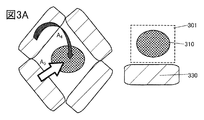
- FIG. 3A is a conceptual diagram of a conventional guest material.
- FIG. 3B is a conceptual diagram of a guest material used for the light-emitting device of one embodiment of the present invention.
- FIG. 4A is a structural formula of a guest material used for the light-emitting device of one embodiment of the present invention.
- FIG. 4B is a ball-and-stick diagram of a guest material used in the light-emitting device of one embodiment of the present invention.
- FIG. 5A is a schematic sectional view of a light emitting layer of a light emitting device of one embodiment of the present invention.
- 5B to 5D are diagrams illustrating the correlation of energy levels of the light emitting layer of the light emitting device of one embodiment of the present invention.
- FIG. 6A is a schematic sectional view of a light emitting layer of a light emitting device of one embodiment of the present invention.
- 6B and 6C are diagrams illustrating the correlation of energy levels of the light emitting layer of the light emitting device of one embodiment of the present invention.
- FIG. 7A is a schematic sectional view of a light emitting layer of a light emitting device of one embodiment of the present invention.
- 7B and 7C are diagrams illustrating the correlation of energy levels of the light emitting layer of the light emitting device of one embodiment of the present invention.
- FIG. 8A is a schematic sectional view of a light emitting layer of a light emitting device of one embodiment of the present invention.
- 8B and 8C are diagrams illustrating the correlation of energy levels of the light emitting layer of the light emitting device of one embodiment of the present invention.
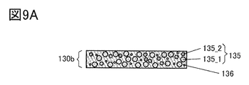
- FIG. 9A is a schematic sectional view of a light emitting layer of a light emitting device of one embodiment of the present invention.
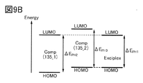
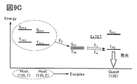
- FIG. 9B and 9C are diagrams illustrating the correlation of energy levels of the light emitting layer of the light emitting device of one embodiment of the present invention.
- FIG. 10A is a schematic sectional view of a light emitting layer of a light emitting device of one embodiment of the present invention.
- 10B and 10C are diagrams illustrating the correlation of energy levels of the light emitting layer of the light emitting device of one embodiment of the present invention.
- FIG. 11A is a schematic sectional view of a light emitting layer of a light emitting device of one embodiment of the present invention.
- FIG. 11B is a diagram illustrating a correlation of energy levels of a light emitting layer of a light emitting device of one embodiment of the present invention.
- FIG. 10A is a schematic sectional view of a light emitting layer of a light emitting device of one embodiment of the present invention.
- FIG. 11B is a diagram illustrating a correlation of energy levels of a light emitting layer of a light emitting device of one embodiment
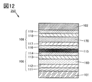
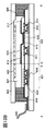
- FIG. 12 is a schematic cross-sectional view of a light emitting device of one embodiment of the present invention.
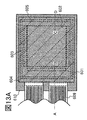
- FIG. 13A is a top view illustrating a display device of one embodiment of the present invention.
- FIG. 13B is a schematic cross-sectional view illustrating the display device of one embodiment of the present invention.
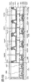
- 14A and 14B are schematic cross-sectional views each illustrating a display device of one embodiment of the present invention.
- 15A and 15B are schematic cross-sectional views each illustrating a display device of one embodiment of the present invention.
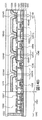
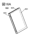
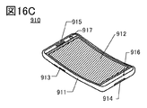
- 16A to 16D are perspective views illustrating a display module of one embodiment of the present invention.
- 17A to 17C are diagrams illustrating electronic devices of one embodiment of the present invention.
- 18A and 18B are perspective views each illustrating a display device of one embodiment of the present invention.
- FIG. 19 is a diagram illustrating a lighting device of one embodiment of the present invention.
- the ordinal numbers given as the first, second, etc. are used for convenience, and may not indicate the process order or the stacking order. Therefore, for example, the description can be made by appropriately replacing “first” with “second” or “third”.
- the ordinal numbers described in this specification and the like may be different from the ordinal numbers used to specify one embodiment of the present invention.
- film and “layer” can be interchanged with each other.
- conductive layer to the term “conductive film”.
- insulating film to the term “insulating layer”.
- a singlet excited state is a singlet state having excitation energy.
- the S1 level is the lowest singlet excitation energy level, and is the lowest singlet excited state (S1 state) excitation energy level.
- a triplet excited state (T * ) is a triplet state having excitation energy.
- the T1 level is the lowest triplet excitation energy level, and is the lowest triplet excited state (T1 state) excitation energy level. Note that in this specification and the like, the S1 state and the S1 level may be expressed even if they are simply described as a singlet excited state and a singlet excited energy level. Further, even when described as a triplet excited state and a triplet excited energy level, it may represent the T1 state and the T1 level.
- the fluorescent material is a compound that emits light in the visible light region when relaxing from the singlet excited state to the ground state.
- a phosphorescent material is a compound that emits light in the visible light region at room temperature when the triplet excited state is relaxed to the ground state.
- the phosphorescent material is one of compounds capable of converting triplet excitation energy into visible light.
- the blue wavelength region is 400 nm or more and less than 490 nm, and blue light emission has at least one emission spectrum peak in the wavelength region.
- the green wavelength region is 490 nm or more and less than 580 nm, and the green emission has at least one emission spectrum peak in the wavelength region.
- the red wavelength region is 580 nm or more and 680 nm or less, and red emission has at least one emission spectrum peak in the wavelength region.
- a light-emitting layer is a layer containing one or more kinds of fluorescent materials or phosphorescent materials.
- the fluorescent light emitting layer is a layer from which light emission having fluorescent light emission is obtained
- the phosphorescent light emitting layer is a layer from which light emission having phosphorescent light emission is obtained.
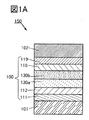
- FIG. 1A and 1B are schematic cross-sectional views of a light emitting device 150 and a light emitting device 152 according to one embodiment of the present invention.
- Each of the light emitting device 150 and the light emitting device 152 has a pair of electrodes (the electrode 101 and the electrode 102) and the EL layer 100 or the EL layer 200 provided between the pair of electrodes.
- the EL layers 100 and 200 each include at least a light emitting layer 130a and a light emitting layer 130b.
- the EL layer 100 illustrated in FIG. 1A has functional layers such as a hole injection layer 111, a hole transport layer 112, an electron transport layer 118, and an electron injection layer 119 in addition to the light emitting layers 130a and 130b.
- the EL layer 200 illustrated in FIG. 1B further includes a separation layer 120. That is, the EL layer 200 has a structure in which the separation layer 120 is added to the EL layer 100.
- the electrode 101 of the pair of electrodes will be described as the anode and the electrode 102 will be described as the cathode, but the configurations of the light emitting device 150 and the light emitting device 152 are not limited thereto. That is, the electrode 101 may be the cathode, the electrode 102 may be the anode, and the layers of the layers between the electrodes may be laminated in the reverse order. That is, the hole injection layer 111, the hole transport layer 112, the light emitting layer 130a, the light emitting layer 130b, the electron transport layer 118, and the electron injection layer 119 may be stacked in this order from the anode side. ..
- the hole transport layer 112 and the light emitting layer 130a are adjacent to each other, and the electron transport layer 118 and the light emitting layer 130b are adjacent to each other, the light emitting device 150 and the light emitting device 152 are configured as follows. Is not the case. That is, in the light emitting device 150 and the light emitting device 152, the hole transport layer 112 and the light emitting layer 130b may be adjacent to each other, and the electron transport layer 118 and the light emitting layer 130a may be adjacent to each other.
- the structures of the EL layer 100 and the EL layer 200 are not limited to those illustrated in FIGS. 1A and 1B, and may be any of the hole injection layer 111, the hole transport layer 112, the electron transport layer 118, and the electron injection layer 119. It suffices to adopt a configuration having at least one selected from Alternatively, the EL layer 100 and the EL layer 200 reduce an injection barrier of holes or electrons, improve transportability of holes or electrons, inhibit transportability of holes or electrons, or have an electrode quenching phenomenon. It may be configured to have a functional layer having a function of suppressing or the like.
- the functional layers may each be a single layer or a structure in which a plurality of layers are laminated.
- the light-emitting layer 130a is described as a fluorescent light-emitting layer containing a fluorescent material
- the light-emitting layer 130b is described as a phosphorescent light-emitting layer containing a phosphorescent material. Therefore, both fluorescence emission and phosphorescence emission can be obtained from the light-emitting device of one embodiment of the present invention.
- the light-emitting device 150 and the light-emitting device 152 of one embodiment of the present invention by applying a voltage between the pair of electrodes (the electrode 101 and the electrode 102), electrons are emitted from the cathode and holes are emitted from the anode, respectively.
- a current flows.
- excitons generated by recombination of carriers electrons and holes
- the ratio of singlet excitons to triplet excitons hereinafter, exciton generation probability
- the proportion of singlet excitons generated is 25% and the proportion of triplet excitons generated is 75%.
- Phosphorescent materials are examples of materials that have the function of converting triplet excitation energy into luminescence.
- a phosphorescent material refers to a compound that exhibits phosphorescence and does not emit fluorescence in any of a temperature range of low temperature (eg, 77 K) to room temperature (ie, 77 K to 313 K). ..
- the phosphorescent material preferably contains a metal element having a large spin-orbit interaction, specifically a transition metal element, particularly a platinum group element (ruthenium (Ru), rhodium (Rh), palladium (Pd), osmium). It is preferable to have (Os), iridium (Ir), or platinum (Pt), and iridium is particularly preferable.
- the presence of Ir can increase the transition probability associated with the direct transition between the singlet ground state and the triplet excited state.
- a TADF material As a material having a function of converting triplet excitation energy into light emission, a TADF material can be mentioned.
- the TADF material is a material having a small difference between the S1 level and the T1 level and capable of converting energy from triplet excitation energy to singlet excitation energy by the intersystem crossing. Therefore, the triplet excitation energy can be up-converted (reverse intersystem crossing) to a singlet excitation energy with a small amount of thermal energy, and a singlet excited state can be efficiently generated.
- an exciplex (also referred to as an exciplex, an exciplex, or an exciplex) that forms an excited state with two kinds of substances has an extremely small difference between the S1 level and the T1 level, and has triplet excitation energy as singlet excitation energy. It has a function as a TADF material that can be converted into.
- a phosphorescence spectrum observed at low temperature may be used as an index of the T1 level.
- a tangent line is drawn at the short wavelength side skirt of the fluorescence spectrum at room temperature or low temperature
- the energy of the wavelength of the extrapolation line is set to the S1 level
- a tangent line is drawn at the short wavelength side skirt of the phosphorescence spectrum.
- the difference between S1 and T1 is preferably 0.2 eV or less.
- a nanostructure of a transition metal compound having a perovskite structure can be mentioned.
- nanostructures of metal halide perovskites are preferable.
- nanoparticles and nanorods are preferable.
- FIG. 2A is a schematic sectional view showing a light emitting layer 130a of a light emitting device which is one embodiment of the present invention.
- the light emitting layer 130a includes the compound 131 and the compound 132.
- the compound 131 has a function of converting triplet excitation energy into light emission
- the compound 132 has a function of converting singlet excitation energy into light emission. Since a fluorescent material has high stability, it is preferable to use a fluorescent material as the compound 132 in order to obtain a highly reliable light emitting device. Since the compound 131 has a function of converting triplet excitation energy into light emission, carrier recombination occurs in the compound 131 in order to obtain a light-emitting device with high emission efficiency.
- both singlet excitation energy and triplet excitation energy of excitons generated by recombination of carriers in the compound 131 finally transfer energy to the singlet excited state of the compound 132 and the compound 132 emits light.
- the compound 131 is an energy donor and the compound 132 is an energy acceptor.
- the light emitting layer 130a is a fluorescent light emitting layer using the compound 131 as a host material and the compound 132 as a guest material. That is, in FIGS. 2A and 2B, the host material has a function as an energy donor and the guest material has a function as an energy acceptor. Further, the light emitting layer 130a can obtain light emission derived from the compound 132 which is a guest material.
- FIG. 2B is an example of energy level correlation in a light emitting layer in a light emitting device of one embodiment of the present invention. This structural example shows the case where a TADF material is used for the compound 131.
- FIG. 2B shows the energy level correlation between the compound 131 and the compound 132 in the light emitting layer 130a.
- the vertical axis of FIG. 2B represents energy (arbitrary unit).
- the notations and symbols in FIG. 2B are as follows.
- the compound 131 has TADF property. Therefore, the compound 131 has a function of converting triplet excitation energy into singlet excitation energy by upconversion (FIG. 2B route A 1 ).
- the singlet excitation energy of the compound 131 can be quickly transferred to the compound 132. (FIG. 2B route A 2 ).
- S C1 ⁇ S G it is preferable that S C1 ⁇ S G.
- a tangent line is drawn at the skirt on the short wavelength side of the fluorescence spectrum of the compound 131, the energy of the wavelength of the extrapolation line is S C1, and the energy of the wavelength of the absorption edge of the absorption spectrum of the compound 132 is S G. In doing so, it is preferable that S C1 ⁇ S G. Since the compound 131 is a material having TADF property, S C1 and T C1 are very small. Therefore, S C1 ⁇ S T1 ⁇ S G.
- the triplet excitation energy generated in the compound 131 transfers energy to the S1 level of the compound 132, which is the guest material, through the routes A 1 and A 2 described above, and the compound 132 emits light, thereby improving the emission efficiency of the fluorescent light emitting device. Can be increased.
- Route A 2 the compound 131 functions as an energy donor and the compound 132 functions as an energy acceptor.
- the compound 131 and the compound 132 are mixed in the light emitting layer 130a. Therefore, a process in which the triplet excitation energy of the compound 131 is converted into the triplet excitation energy of the compound 132 in competition with the routes A 1 and A 2 (FIG. 2B, route A 3 ) may occur. Since the compound 132 is a fluorescent material, the triplet excitation energy of the compound 132 does not contribute to light emission. That is, if the energy transfer of the route A 3 occurs, the luminous efficiency of the light emitting device will decrease. In reality, energy transfer from T C1 to T G (route A 3 ) is not direct, but energy transfer once to a triplet excited state higher than T G of compound 132, and then becomes T G by internal conversion. There may be a route, but the process is omitted in the figure. The subsequent undesired heat deactivation process in the present specification, that is, the deactivation process to TG is all the same.
- the Forster mechanism dipole-dipole interaction
- the Dexter mechanism electron exchange interaction
- the compound 132 which is an energy acceptor
- the Dexter mechanism is dominant in the energy transfer of route A 3 .
- the Dexter mechanism significantly occurs when the distance between the compound 131 which is an energy donor and the compound 132 which is an energy acceptor is 1 nm or less. Therefore, in order to suppress the route A 3 , it is important to increase the distance between the host material and the guest material, that is, the distance between the energy donor and the energy acceptor.
- the concentration of the energy acceptor in the mixed film of these compounds may be lowered.
- the concentration of the energy acceptor in the mixed film is reduced, not only the energy transfer from the energy donor to the energy acceptor based on the Dexter mechanism but also the energy transfer based on the Forster mechanism is suppressed. In that case, since the route A 2 is based on the Forster mechanism, problems such as a decrease in light emitting efficiency and a decrease in reliability of the light emitting device occur.
- the inventors of the present invention can suppress the above-mentioned decrease in luminous efficiency and decrease in reliability by using a fluorescent material having a protective group for increasing the distance from the energy donor as the energy acceptor. I found it. Further, they have found that it is possible to suppress a decrease in the luminous efficiency of the phosphorescent emitting layer which occurs when the phosphorescent emitting layer and the fluorescent emitting layer are combined.
- FIG. 3A shows a conceptual diagram in which a fluorescent material having no protective group, which is a general fluorescent material, is dispersed as a guest material in a host material
- FIG. 3B shows a light emitting device of one embodiment of the present invention.
- the conceptual diagram in the case of using the fluorescent material which has a protective group and is used as a guest material and disperse
- the host material may be read as an energy donor and the guest material may be read as an energy acceptor.
- the protective group has a function of increasing the distance between the luminophore and the host material.
- the guest material 301 has a luminophore 310.
- the guest material 301 has a function as an energy acceptor.
- the guest material 302 has a luminophore 310 and a protective group 320.
- the guest material 301 and the guest material 302 are surrounded by the host material 330. Since the distance between the luminophore and the host material is short in FIG. 3A, energy transfer from the host material 330 to the guest material 301 is performed by energy transfer by the Forster mechanism (route A 4 in FIGS. 3A and 3B) and energy by the Dexter mechanism. Both movement (route A 5 in FIGS. 3A and 3B) can occur.
- the triplet excited state of the guest material is generated by energy transfer of the triplet excited energy from the host material to the guest material by the Dexter mechanism, the triplet excited energy is non-radiatively deactivated when the guest material is a fluorescent material. Therefore, it is one of the causes of the decrease in luminous efficiency.
- the guest material 302 has a protective group 320. Therefore, the distance between the luminescent group 310 and the host material 330 can be increased. Therefore, energy transfer (route A 5 ) by the Dexter mechanism can be suppressed.
- the guest material 302 in order for the guest material 302 to emit light, since the Dexter mechanism is suppressed, the guest material 302 needs to receive energy from the host material 330 by the Forster mechanism. That is, it is preferable to efficiently use the energy transfer by the Forster mechanism while suppressing the energy transfer by the Dexter mechanism. It is known that energy transfer by the Forster mechanism is also affected by the distance between the host material and the guest material. Generally, when the distance between the host material 330 and the guest material 302 is 1 nm or less, the Dexter mechanism is dominant, and when the distance is 1 nm or more and 10 nm or less, the Forster mechanism is dominant.
- the distance between the host material 330 and the guest material 302 is 10 nm or more, energy transfer hardly occurs.
- the distance between the host material 330 and the guest material 302 may be read as the distance between the host material 330 and the light-emitting group 310.
- the protective group 320 extends from the luminophore 310 to a range of 1 nm or more and 10 nm or less. More preferably, it is 1 nm or more and 5 nm or less. With this structure, energy transfer by the Forster mechanism can be efficiently used while suppressing energy transfer from the host material 330 to the guest material 302 by the Dexter mechanism. Therefore, a light emitting device having high luminous efficiency can be manufactured.
- the concentration of the guest material 301 or the guest material 302 with respect to the host material 330.
- the concentration of the guest material is increased, the energy transfer speed of the Dexter mechanism is also increased, and the luminous efficiency is decreased. Therefore, it was difficult to increase the concentration of the guest material.
- a fluorescent light emitting device in which a material having a function of converting triplet excitation energy into light emission is used as a host material, a light emitting device having a low guest material concentration of 1 wt% or less has been reported.
- a guest material having a protective group in a light-emitting group is used for a light-emitting layer. Therefore, the energy transfer by the Forster mechanism can be efficiently used while suppressing the energy transfer by the Dexter mechanism, so that the concentration of the guest material that is the energy acceptor can be increased. As a result, an originally contradictory phenomenon of increasing the energy transfer speed by the Forster mechanism while suppressing the energy transfer by the Dexter mechanism can be enabled. By increasing the energy transfer rate by the Forster mechanism, the excitation lifetime of the energy acceptor in the light emitting layer is shortened, so that the reliability of the light emitting device can be improved.
- the concentration of the guest material is preferably 2 wt% or more and 30 wt% or less with respect to the host material, more preferably 5 wt% or more and 20 wt% or less, and further preferably 5 wt% or more and 15 wt% or less.
- the concentration of the guest material is preferably 2 wt% or more and 30 wt% or less with respect to the host material, more preferably 5 wt% or more and 20 wt% or less, and further preferably 5 wt% or more and 15 wt% or less.
- the light emitting efficiency can be improved by using a fluorescent material having high stability, a light emitting device with favorable reliability can be manufactured.
- the above concentration is a concentration in a case where a material that mainly emits light is a guest material and a material other than the guest material is a host material in the light emitting layer.
- the effect of the light-emitting device of one embodiment of the present invention is not only the effect of improving reliability by using a fluorescent material with high stability.
- the energy transfer as described above always competes with the quenching process due to the influence of deteriorated substances and impurities.
- the rate of light emitted by the light emitting device decreases. That is, the brightness of the light emitting device deteriorates.
- one embodiment of the present invention can suppress energy transfer by the Dexter mechanism and increase the energy transfer speed by the Forster mechanism as compared with a conventional light-emitting device; thus, the influence of competition with the quenching process. Can be made smaller and the life of the device can be extended.
- the luminescent group refers to an atomic group (skeleton) that causes light emission in the fluorescent material.
- the luminophore generally has a ⁇ bond, preferably contains an aromatic ring, and preferably has a condensed aromatic ring or a condensed heteroaromatic ring.
- the luminophore can be regarded as an atomic group (skeleton) including an aromatic ring having a transition dipole vector on the ring plane.
- the skeleton having the lowest S1 level among the plurality of condensed aromatic rings or condensed heteroaromatic rings is used as the fluorescent material.
- the skeleton having the absorption edge at the longest wavelength may be considered as the luminescent group of the fluorescent material.
- the luminophore of the fluorescent material can be predicted from the shape of the emission spectrum of each of the plurality of condensed aromatic rings or the condensed heteroaromatic rings.
- Examples of the condensed aromatic ring or the condensed heteroaromatic ring include a phenanthrene skeleton, a stilbene skeleton, an acridone skeleton, a phenoxazine skeleton, and a phenothiazine skeleton.
- a fluorescent material having a naphthalene skeleton, anthracene skeleton, fluorene skeleton, chrysene skeleton, triphenylene skeleton, tetracene skeleton, pyrene skeleton, perylene skeleton, coumarin skeleton, quinacridone skeleton, and naphthobisbenzofuran skeleton is preferable because of high fluorescence quantum yield.
- the substituent used as the protective group needs to have a triplet excitation energy level higher than the T1 level of the luminophore and the host material. Therefore, it is preferable to use a saturated hydrocarbon group. This is because the substituent having no ⁇ bond has a high triplet excitation energy level. Further, a substituent having no ⁇ bond has a low function of transporting carriers (electrons or holes). Therefore, the saturated hydrocarbon group can increase the distance between the luminophore and the host material without affecting the excited state of the host material or the carrier transport property.
- the frontier orbital ⁇ HOMO Highest Occupied Molecular Orbital, and the highest occupied molecular orbital are present
- LUMO Large Unoccupied Molecular Orbital, also referred to as the lowest unoccupied orbit
- the luminophore often has a frontier orbit.
- overlapping of HOMO of energy donor and energy acceptor and overlapping of LUMO are important.
- the distance between the frontier orbital of the host material, which is the energy donor, and the frontier orbital of the guest material, which is the energy acceptor, can be increased, and energy transfer by the Dexter mechanism can be achieved. Can be suppressed.
- the protective group examples include an alkyl group having 1 to 10 carbon atoms. Further, since the protective group needs to increase the distance between the luminophore and the host material, a bulky substituent is preferable. Therefore, an alkyl group having 3 to 10 carbon atoms, a substituted or unsubstituted cycloalkyl group having 3 to 10 carbon atoms, or a trialkylsilyl group having 3 to 12 carbon atoms can be preferably used. Particularly, as the alkyl group, a bulky branched chain alkyl group is preferable. Further, it is particularly preferable that the substituent has a quaternary carbon because it becomes a bulky substituent.
- one luminophore has five or more protecting groups.
- the entire luminophore can be covered with the protective group, so that the distance between the host material and the luminophore can be appropriately adjusted.
- FIG. 3B shows a state in which the luminophore and the protective group are directly bonded, but it is more preferable that the protective group is not directly bonded to the luminophore.
- the protecting group may be bonded to the luminophore through a divalent or higher valent substituent such as an arylene group or an amino group.
- the protective group is bonded to the luminophore through the substituent, the distance between the luminophore and the host material can be effectively increased. Therefore, when the luminophore and the protecting group are not directly bonded, if four or more protecting groups are provided for one luminophore, the energy transfer due to the Dexter mechanism can be effectively suppressed.
- the divalent or higher valent substituent that connects the luminescent group and the protective group is preferably a substituent having a ⁇ -conjugated system. With such a structure, physical properties such as an emission color of the guest material, a HOMO level, and a glass transition point can be adjusted.
- the protective group is preferably arranged on the outermost side when the molecular structure is centered around the luminophore.
- N,N′-[(2-tert-butylanthracene)-9,10- which is a fluorescent material represented by the following structural formula (102) and can be used for the light-emitting device of one embodiment of the present invention.
- the structure of diyl]-N,N'-bis(3,5-di-tert-butylphenyl)amine (abbreviation: 2tBu-mmtBuDPhA2Anth) is shown.
- 2tBu-mmtBuDPhA2Anth the anthracene ring is a luminescent group, and the tertiary butyl (tBu) group acts as a protective group.
- FIG. 4B shows a state when 2tBu-mmtBuDPhA2Anth is viewed from the direction of the arrow in FIG. 4A (horizontal direction with respect to the anthracene ring surface).
- the shaded portion in FIG. 4B represents the portion directly above the anthracene ring surface that is the luminescent group, and it can be seen that there is a region where the tBu group, which is a protecting group, overlaps with the portion directly above this.
- the atom indicated by the arrow (a) is a carbon atom of the tBu group overlapping with the shaded portion
- the atom indicated by the arrow (b) is a hydrogen atom of the tBu group overlapping with the shaded portion.
- the distance between the anthracene ring and the host material can be increased in both the plane direction and the vertical direction of the anthracene ring that is the luminescent group, Energy transfer due to the Dexter mechanism can be suppressed.
- the Dexter mechanism significantly occurs when the HOMO and LUMO of both materials overlap. Therefore, in order to suppress the Dexter mechanism, it is important to suppress the overlap of HOMO and LUMO of both materials. That is, it is important to increase the distance between the skeleton related to the excited state and the host material.
- the luminophore often has both HOMO and LUMO.
- the HOMO and LUMO of the guest material are spread above and below the surface of the luminophore (in the case of 2tBu-mmtBuDPhA2Anth, above and below the anthracene ring), they cover the above and below the surface of the luminophore with protective groups. Is important in the molecular structure.
- the upper side and the lower side of the anthracene ring represent the upper side and the lower side with the anthracene ring surface as the reference plane when viewed from the arrow in FIG. 4A.
- a protective group such as a tBu group is arranged so as to cover a luminescent group such as an anthracene ring.
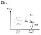
- FIG. 5C is an example of a correlation of energy levels in the light emitting layer 130a of the light emitting device 150 and the light emitting device 152 according to one embodiment of the present invention.
- the light-emitting layer 130a illustrated in FIG. 5A includes the compound 131, the compound 132, and the compound 133.
- compound 132 is preferably a fluorescent material.
- the compound 131 and the compound 133 are a combination that forms an exciplex.
- the combination of the compound 131 and the compound 133 may be a combination capable of forming an exciplex, but one is a compound having a function of transporting holes (hole transporting property) and the other is a compound of electrons.
- a compound having a transporting function is more preferable.
- a donor-acceptor type exciplex can be easily formed, and an exciplex can be efficiently formed.
- the carrier balance can be easily controlled by the mixing ratio.
- the range of compound having hole transporting property: compound having electron transporting property 1:9 to 9:1 (weight ratio) is preferable.
- the carrier balance can be easily controlled by having the structure, the carrier recombination region can be easily controlled.
- one of the compound 131 and the compound 133 has a higher HOMO level than the other HOMO level, and one LUMO level higher than the other LUMO level. It is preferable.
- the HOMO level of the compound 131 may be equivalent to the HOMO level of the compound 133, or the LUMO level of the compound 131 may be equivalent to the LUMO level of the compound 133.
- the LUMO level and HOMO level of a compound can be derived from the electrochemical characteristics (reduction potential and oxidation potential) of the compound measured by cyclic voltammetry (CV) measurement.
- the HOMO level of the compound 131 is higher than the HOMO level of the compound 133 as shown in the energy band diagram in FIG. 5B.
- the LUMO level of the compound 131 is preferably higher than the LUMO level of the compound 133.
- Comp(131) represents the compound 131
- Comp(133) represents the compound 133
- ⁇ E C1 represents the energy difference between the LUMO level and the HOMO level of the compound 131
- ⁇ E C3 represents the compound.
- 133 represents the energy difference between the LUMO level and the HOMO level of 133
- ⁇ E E is a notation and code indicating the energy difference between the LUMO level of the compound 131 and the HOMO level of the compound 133.
- the excitation energy of the exciplex approximately corresponds to the energy difference ( ⁇ E E ) between the LUMO level of the compound 133 and the HOMO level of the compound 131, and the energy difference between the LUMO level and the HOMO level of the compound 131. ( ⁇ E C1 ) and the energy difference ( ⁇ E C3 ) between the LUMO level and the HOMO level of Compound 133. Therefore, by forming an exciplex with the compound 131 and the compound 133, it becomes possible to form an excited state with lower excitation energy. Further, since it has a lower excitation energy, the exciplex can form a stable excited state.
- FIG. 5C shows the correlation of the energy levels of the compound 131, the compound 132, and the compound 133 in the light emitting layer 130a.
- -Comp(131) Compound 131
- -Comp(133) Compound 133 ⁇ Guest (132): Compound 132
- S C1 S1 level of compound 131.
- T C1 T1 level of compound 131.
- S C3 S1 level of compound 133.
- T C3 S1 level of compound 133.
- T G T1 level of compound 132.
- the compound 131 and the compound 133 included in the light-emitting layer 130a form an exciplex.
- the S1 level (S E ) of the exciplex and the T1 level (T E ) of the exciplex are energy levels adjacent to each other (see route A 6 in FIG. 5C).
- the excitation energy levels (S E and T E ) of the exciplex are lower than the S1 levels (S C1 and S C3 ) of the substances (compound 131 and compound 133) forming the exciplex, lower excitation energy is obtained.
- the excited state can be formed by. Accordingly, the driving voltage of the light-emitting device of one embodiment of the present invention can be reduced.
- the exciplex Since the S1 level (S E ) and the T1 level (T E ) of the exciplex are energy levels adjacent to each other, the inter-reciprocal intersections easily occur and TADF property is exhibited. Therefore, the exciplex has a function of converting triplet excitation energy into singlet excitation energy by upconversion (FIG. 5C, route A 7 ). The singlet excitation energy of the exciplex can quickly move to the compound 132. ( Figure 5C route A 8). At this time, it is preferable that S E ⁇ S G. In Route A 8 , the exciplex is the energy donor and compound 132 functions as the energy acceptor.
- a tangent line is drawn at the short wavelength side skirt of the fluorescence spectrum of the exciplex, the energy of the wavelength of the extrapolation line is S E, and the energy of the wavelength of the absorption edge of the absorption spectrum of the compound 132 is S G. In doing so, it is preferable that S E ⁇ S G.
- the T1 levels of both the compound 131 and the compound 133 are equal to or higher than T E.
- the index it is preferable that the shortest emission peak wavelengths of the phosphorescence spectra of the compound 131 and the compound 133 are both less than or equal to the maximum emission peak wavelength of the exciplex.
- a tangent line is drawn at the short wavelength side skirt of the fluorescence spectrum of the exciplex, the energy of the wavelength of the extrapolation line is S E, and a tangent line is drawn at the short wavelength side skirt of the compound 131 and compound 133, respectively.
- S E ⁇ T C1 ⁇ 0.2 eV and S E ⁇ T C3 ⁇ 0.2 eV when the energy of the wavelength of the extrapolated line is T C1 and T C3 of each compound. ..
- the guest material emits light by the triplet excitation energy generated in the light emitting layer 130a passing through energy transfer (route A 8 ) from the S1 level of the above-mentioned route A 6 and exciplex to the S1 level of the guest material. be able to. Therefore, by using a combination of materials that form an exciplex in the light emitting layer 130a, it is possible to increase the light emission efficiency of the fluorescent light emitting device.
- a guest material having a protective group in a light-emitting group is used for the compound 132.
- energy transfer by the Dexter mechanism represented by route A 9 can be suppressed, and deactivation of triplet excitation energy can be suppressed. Therefore, a fluorescent light emitting device device having high luminous efficiency can be obtained.
- the processes of the routes A 6 to A 8 described above may be referred to as “Exset-Singlet Energy Transfer” or “ExEF (Enhanced-Enhanced Fluorescence)”.
- ExEF Enhanced-Enhanced Fluorescence
- the light emitting layer 130a has donation of excitation energy from the exciplex to the fluorescent material.
- a compound having a heavy atom is used as one of the compounds forming the exciplex. Therefore, intersystem crossing between the singlet state and the triplet state is promoted. Therefore, an exciplex capable of transition from the triplet excited state to the singlet ground state (that is, capable of exhibiting phosphorescence) can be formed.
- the triplet excitation energy level (T E ) of the exciplex becomes an energy donor level, so that T E is a singlet excitation energy level of the compound 132 which is a light-emitting material. It is preferably at least (S G ).
- a tangent line is drawn at the short-wavelength side skirt of the emission spectrum of an exciplex in which one compound has a heavy atom, and the energy of the wavelength of the extrapolation line is set to T E, and the absorption of the compound 132 is absorbed.
- T E the energy of the wavelength of the absorption edge of the spectrum upon the S G.
- S G compound 132 from the triplet excited energy level of the exciplex (T E) Energy can be transferred to.
- S1 quasi-position of the exciplex (S E) and the T1 level position (T E) are the energy levels adjacent to each other, in an emission spectrum, when it is difficult to clearly distinguish between fluorescence and phosphorescence There is. In that case, it may be possible to distinguish between fluorescence and phosphorescence depending on the emission lifetime.
- the phosphorescent material used in the above structure preferably contains a heavy atom such as Ir, Pt, Os, Ru, or Pd.
- the quantum yield may be high or low. That is, the energy transfer from the triplet excitation energy level of the exciplex to the singlet excitation energy level of the guest material may be allowed transition.
- the energy transfer from the exciplex composed of the phosphorescent material or the phosphorescent material to the guest material as described above is performed from the triplet excitation energy level of the energy donor to the singlet excitation energy level of the guest material (energy acceptor). Is preferable because the energy transfer to is an allowable transition.
- the triplet excitation energy of the exciplex can be transferred to the S1 level (S G ) of the guest material by the process of route A 8 without passing through the process of route A 7 in FIG. 5C. That is, the triplet and singlet excitation energies can be transferred to the S1 level of the guest material only in the processes of route A 6 and route A 8 .
- the exciplex is the energy donor and compound 132 functions as the energy acceptor.
- a guest material having a protective group in a light-emitting group is used for the compound 132.
- energy transfer by the Dexter mechanism represented by route A 9 can be suppressed, and deactivation of triplet excitation energy can be suppressed. Therefore, a fluorescent light emitting device with high luminous efficiency can be obtained.
- the compound 133 Since the compound 133 is a TADF material, the compound 133 that does not form an exciplex has a function of converting triplet excitation energy into singlet excitation energy by upconversion (FIG. 5D route A 10 ). The singlet excitation energy of the compound 133 can quickly move to the compound 132. (FIG. 5D Route A 11 ). At this time, it is preferable that S C3 ⁇ S G.
- a route in which triplet excitation energy moves to the compound 132 which is a guest material through the route A 6 to the route A 8 in FIG. 5D. Then, there is a route to move to the compound 132 via route A 10 and route A 11 in FIG. 5D. Since there are multiple paths through which the triplet excitation energy moves to the fluorescent material, the light emission efficiency can be further increased.
- the exciplex is the energy donor and compound 132 functions as the energy acceptor.
- compound 133 is an energy donor and compound 132 functions as an energy acceptor.
- the exciplex and the compound 133 are energy donors, and the compound 132 functions as an energy acceptor.
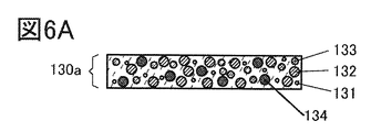
- FIG. 6A shows the case where four kinds of materials are used for the light emitting layer 130a.
- the light emitting layer 130a includes a compound 131, a compound 132, a compound 133, and a compound 134.
- the compound 133 has a function of converting triplet excitation energy into light emission.
- the compound 133 is a phosphorescent compound will be described.
- the compound 132 is a guest material that exhibits fluorescence emission.
- the compound 131 is an organic compound that forms an exciplex with the compound 134.
- FIG. 6B shows the correlation of energy levels of the compound 131, the compound 132, the compound 133, and the compound 134 in the light emitting layer 130a.
- the notations and symbols in FIG. 6B are as follows, and the other notations and symbols are the same as the notations and symbols shown in FIG. 5C.
- S C4 S1 level of compound 134
- T C4 T1 level of compound 134
- the compound 131 and the compound 134 included in the light-emitting layer 130a form an exciplex.
- the exciplex formed in the above process loses its excitation energy, and the two kinds of substances that formed the exciplex behave as the original separate substances.
- the excitation energy levels (S E and T E ) of the exciplex are lower than the S1 levels (S C1 and S C4 ) of the substances (compound 131 and compound 134) forming the exciplex, the excitation energy is lower. It is possible to form an excited state with. Thereby, the drive voltage of the light emitting device 150 and the light emitting device 152 can be reduced.
- the compound 133 when the compound 133 is a phosphorescent material, the intersystem crossing between the singlet state and the triplet state is allowed. Therefore, both the singlet excitation energy and the triplet excitation energy of the exciplex rapidly move to the compound 133 (route A 13 ). At this time, it is preferable that T E ⁇ T C3 . Further, the triplet excitation energy of the compound 133 can be efficiently converted into the singlet excitation energy of the compound 132 (route A 14 ).
- T E ⁇ T C3 ⁇ S G is preferable because the excitation energy of the compound 133 is efficiently transferred to the compound 132 which is a guest material as singlet excitation energy.
- a tangent line is drawn at the short wavelength side skirt of the phosphorescence spectrum of the compound 133, the energy of the wavelength of the extrapolation line is T C3, and the energy of the wavelength of the absorption edge of the absorption spectrum of the compound 132 is S G. In doing so, it is preferable that T C3 ⁇ S G.
- compound 133 functions as an energy donor and compound 132 functions as an energy acceptor.
- the combination of the compound 131 and the compound 134 may be a combination capable of forming an exciplex, but one is a compound having a hole transporting property and the other is a compound having an electron transporting property. More preferably.
- the HOMO level of the compound 131 is higher than the HOMO level of the compound 134 and the LUMO level of the compound 131 is higher than the LUMO level of the compound 134, or the HOMO level of the compound 134 is HOMO of the compound 131. It is preferable that the combination is higher than the level and the LUMO level of the compound 134 is higher than the LUMO level of the compound 131 because an exciplex can be efficiently formed.
- the correlation of the energy levels of the compound 131 and the compound 134 is not limited to FIG. 6B. That is, the singlet excitation energy level (S C1 ) of the compound 131 may be higher or lower than the singlet excitation energy level (S C4 ) of the compound 134. In addition, the triplet excitation energy level (T C1 ) of the compound 131 may be higher or lower than the triplet excitation energy level (T C4 ) of the compound 134.
- the compound 131 preferably has a ⁇ -electron deficient skeleton. With such a structure, the LUMO level of the compound 131 is lowered, which is suitable for formation of an exciplex.
- the compound 131 preferably has a ⁇ -electron excess skeleton. With such a structure, the HOMO level of the compound 131 is increased, which is suitable for formation of an exciplex.
- a guest material having a protective group in a light-emitting group is used for the compound 132.
- energy transfer by the Dexter mechanism represented by route A 15 can be suppressed, and deactivation of triplet excitation energy can be suppressed. Therefore, a fluorescent light emitting device with high luminous efficiency can be obtained.
- concentration of the compound 133 which is an energy donor can be increased. As a result, an originally contradictory phenomenon of increasing the energy transfer speed by the Forster mechanism while suppressing the energy transfer by the Dexter mechanism can be enabled.
- the concentration thereof is preferably 2 wt% or more and 50 wt% or less, more preferably 5 wt% or more and 30 wt% or less, and further preferably 5 wt% or more and 20 wt% with respect to the host material. % Or less.
- the processes of the routes A 12 and A 13 described above may be referred to as ExTET (Exciplex-Triple Energy Transfer) in this specification and the like.
- the light emitting layer 130a has the donation of the excitation energy from the exciplex to the compound 133. Therefore, the present configuration example can be said to be a configuration in which a fluorescent material having a protective group is mixed with a light emitting layer that can use ExTET.
- FIG. 6C shows the case where four kinds of materials are used for the light emitting layer 130a.
- the light emitting layer 130a includes a compound 131, a compound 132, a compound 133, and a compound 134.
- the compound 133 has a function of converting triplet excitation energy into light emission.
- the compound 132 is a guest material that exhibits fluorescence emission.
- the compound 131 is an organic compound that forms an exciplex with the compound 134.
- the compound 134 since the compound 134 is a TADF material, the compound 134 that does not form an exciplex has a function of converting triplet excitation energy into singlet excitation energy by up-conversion (route A 16 in FIG. 6C ). The singlet excitation energy possessed by the compound 134 can be rapidly transferred to the compound 132. (FIG. 6C Route A 17 ).
- S C4 ⁇ S G.
- a tangent line is drawn at the short wavelength side skirt of the fluorescence spectrum of the compound 134, the energy of the wavelength of the extrapolation line is S C4, and the energy of the wavelength of the absorption edge of the absorption spectrum of the compound 132 is S G. In doing so, it is preferable that S C4 ⁇ S G.
- a route in which triplet excitation energy moves to the compound 132 which is a guest material through the route A 12 to the route A 14 in FIG. 6B. Then, there is a route to move to the compound 132 via route A 16 and route A 17 in FIG. 6C. Since there are multiple paths through which the triplet excitation energy moves to the fluorescent material, the light emission efficiency can be further increased.
- compound 133 functions as an energy donor and compound 132 functions as an energy acceptor.
- the compound 134 functions as an energy donor and the compound 132 functions as an energy acceptor.
- FIG. 7B illustrates an example of energy level correlation in the light-emitting layer 130a of the light-emitting device 150 and the light-emitting device 152 of one embodiment of the present invention.
- the light emitting layer 130a illustrated in FIG. 7A includes the compound 131, the compound 132, and the compound 133.
- compound 132 is a fluorescent material having a protecting group.
- the compound 133 has a function of converting triplet excitation energy into light emission. In this structural example, the case where the compound 133 is a phosphorescent material will be described.
- singlet excitons and triplet excitons are generated mainly by carrier recombination in the compound 131 included in the light-emitting layer 130a.
- the compound 133 is a phosphorescent material
- both singlet and triplet excitation energies generated in the compound 131 are transferred to the T C3 level of the compound 133. This can be done (Fig. 7B route A 18 ). Note that some carriers can be recombined with the compound 133.
- the phosphorescent material used in the above structure preferably contains a heavy atom such as Ir, Pt, Os, Ru, or Pd.
- the phosphorescent material acts as an energy donor, so that the quantum yield may be high or low.
- energy transfer from the triplet excitation energy level of the energy donor to the singlet excitation energy level of the guest material (energy acceptor) is an allowable transition, which is preferable. Therefore, the triplet excitation energy of the compound 133 can be transferred to the S1 level (S G ) of the guest material by the process of Route A 19 .
- compound 133 functions as an energy donor and compound 132 functions as an energy acceptor.
- T C3 ⁇ S G because the excitation energy of the compound 133 is efficiently transferred to the singlet excited state of the compound 132 which is a guest material.
- a tangent line is drawn at the short wavelength side skirt of the phosphorescence spectrum of the compound 133, the energy of the wavelength of the extrapolation line is T C3, and the energy of the wavelength of the absorption edge of the absorption spectrum of the compound 132 is S G. In doing so, it is preferable that T C3 ⁇ S G.
- a guest material having a protective group in a light-emitting group is used for the compound 132.
- energy transfer by the Dexter mechanism represented by the route A 20 can be suppressed, and deactivation of triplet excitation energy can be suppressed. Therefore, a fluorescent light emitting device with high luminous efficiency can be obtained.
- FIG. 7C is an example of a correlation of energy levels in the light-emitting device 150 and the light-emitting layer 130a of the light-emitting device of one embodiment of the present invention.
- the light emitting layer 130a illustrated in FIG. 7A includes the compound 131, the compound 132, and the compound 133.
- compound 132 is a fluorescent material having a protecting group.
- the compound 133 has a function of converting triplet excitation energy into light emission. In this structural example, the case where the compound 133 is a compound having a TADF property will be described.
- singlet excitons and triplet excitons are generated mainly by carrier recombination in the compound 131 included in the light-emitting layer 130a.
- a material having a relationship of S C3 ⁇ S C1 and T C3 ⁇ T C1 here, both the singlet excitation energy and the triplet excitation energy generated in the compound 131 are transferred to the S C3 and T C3 levels of the compound 133. It can be moved (Fig. 7C Route A 21 ). Note that some carriers can be recombined with the compound 133.
- compound 133 is a TADF material, it has a function of converting triplet excitation energy into singlet excitation energy by up-conversion (FIG. 7C, route A 22 ). Further, the singlet excitation energy of the compound 133 can be quickly transferred to the compound 132. ( Figure 7C route A 23).
- S C3 ⁇ S G it is preferable that S C3 ⁇ S G. Specifically, a tangent line is drawn on the short wavelength side skirt of the fluorescence spectrum of the compound 133, the energy of the wavelength of the extrapolation line is S C3, and the energy of the wavelength of the absorption edge of the absorption spectrum of the compound 132 is S G. In doing so, it is preferable that S C3 ⁇ S G.
- the triplet excitation energy in the light emitting layer 130a can be converted into the fluorescence emission of the compound 132.
- the compound 133 functions as an energy donor and the compound 132 functions as an energy acceptor.
- a guest material having a protective group in a light-emitting group is used for the compound 132.
- energy transfer by the Dexter mechanism represented by route A 24 can be suppressed, and deactivation of triplet excitation energy can be suppressed. Therefore, a fluorescent light emitting device with high luminous efficiency can be obtained.
- FIG. 8B is an example of a correlation of energy levels in the light emitting layer 130b of the light emitting device 150 and the light emitting device 152 according to one embodiment of the present invention.
- the light emitting layer 130b illustrated in FIGS. 8A, 8B, and 8C includes at least the compound 135 and the compound 136.
- the compound 136 has a function of converting triplet excitation energy into light emission.
- compound 136 is preferably a phosphorescent material.
- 8A, 8B, and 8C show the case where the compound 136 is a phosphorescent material in this structural example.
- FIGS. 8B and 8C The notations and symbols in FIGS. 8B and 8C are as follows.
- singlet excitons and triplet excitons are generated mainly by recombination of carriers in the compound 135 included in the light-emitting layer 130b.
- the compound 136 is a phosphorescent material
- both singlet and triplet excitation energies generated in the compound 135 are transferred to the T PG1 level of the compound 136.
- Can be done (FIGS. 8B and 8C route E 1 ). Note that some carriers can be recombined with the compound 136.
- the absorption band of the longest wavelength in the absorption spectrum of the compound 136 overlaps with the emission spectrum of the compound 135.
- the longest wavelength absorption band of the phosphorescent material is the absorption band that contributes to the strongest emission in the absorption bands included in the entire absorption spectrum.
- examples of the emission spectrum of the compound 135 include a fluorescence spectrum which is light emission derived from a singlet excited state of the compound and a phosphorescence spectrum which is derived from a triplet excited state of the compound.
- both the fluorescence spectrum and the phosphorescence spectrum of the compound 135 overlap with the absorption band of the compound 136 having the longest wavelength.
- the excitation energy of the compound 135 is converted into the excitation energy of the compound 136.
- the energy value of the fluorescence spectrum peak of the compound 135 and the peak of the absorption band of the longest wavelength (low energy side) of the absorption spectrum is preferably 0.2 eV or less. More preferably, it is 0.1 eV or less. With such a structure, a light-emitting layer with high emission efficiency can be obtained.
- the magnitude relationship between the peak energy value of the fluorescence spectrum and the peak value of the absorption band at the longest wavelength (low energy side) of the absorption spectrum does not matter. That is, the energy value of the peak of the fluorescence spectrum may be larger or smaller than the peak value of the absorption band at the longest wavelength (low energy side) of the absorption spectrum.
- the driving voltage of the light emitting device can be reduced while having high light emission efficiency.
- the material having a small energy difference between the S1 level and the T1 level include a TADF material and an exciplex.
- ⁇ Structure Example 2 of Light-Emitting Layer 130b> 9B and 9C are examples of energy level correlations in the light-emitting layer 130b of the light-emitting device 150 and the light-emitting device 152 of one embodiment of the present invention.
- the light-emitting layer 130b illustrated in FIGS. 9A, 9B, and 9C includes at least the compound 135_1, the compound 135_2, and the compound 136.
- the compound 136 has a function of converting triplet excitation energy into light emission.
- compound 136 is preferably a phosphorescent material.
- 9A, 9B, and 9C show the case where the compound 136 is a phosphorescent material in this structural example.
- the compound 135_1 and the compound 135_2 are a combination that forms an exciplex.
- the combination of the compound 135_1 and the compound 135_2 may be a combination capable of forming an exciplex, but one has a function of transporting holes ( More preferably, it is a compound having a hole transporting property, and the other is a compound having a function of transporting an electron (electron transporting property).
- 9B is different from that of FIG. 5B in the reference numerals of the compounds, and the other configurations are the same, and the configurations of the compound 135_1 and the compound 135_2 are the same as the configurations of the compound 131 and the compound 133 in FIG. 5B. Therefore, detailed description of FIG. 9B is omitted.
- Comp(135_1) represents the compound 135_1
- Comp(135_2) represents the compound 135_2
- ⁇ E PH2 represents the energy difference between the LUMO level and the HOMO level of the compound 135_1
- ⁇ E PH3 is the compound.
- 135_2 represents the energy difference between the LUMO level and HOMO level of 135_2
- ⁇ E PH1 is a notation and code indicating the energy difference between the LUMO level of compound 135_1 and the HOMO level of compound 135_2.
- -Host (135_1) Compound 135_1 ⁇ Host (135_2): Compound 135_2 ⁇ Guest (136): Compound 136 • S PH2 : S1 level of compound 135_1 • T PH2 : T1 level of compound 135_1 • S PH3 : S1 level of compound 135_2 • T PH3 : T1 level of compound 135_2 • T PG : T1 level of compound 136 -SPG : S1 level of compound 136- SPE : S1 level of exciplex- TPE : T1 level of exciplex
- One of Compound 135_1 and Compound 135_2 rapidly forms an exciplex by receiving a hole in one and the electron in the other (see Route E 2 in FIG. 9C).
- it when one is in an excited state, it rapidly interacts with the other to form an exciplex.
- the excitation energy level (S PE or T PE ) of the exciplex is lower than the S1 level (S PH1 and S PH2 ) of the host material (compound 135_1 and compound 135_2) forming the exciplex, the excitation energy is lower.
- the drive voltage of the light emitting device can be reduced.
- ExTET The process of the routes E 1 to E 4 described above may be referred to as ExTET in this specification and the like.
- the light emitting layer 130b has the donation of excitation energy from the exciplex to the compound 136. Therefore, in this configuration example, ExTET is applied to the light emitting layer 130b.
- the absorption band of the longest wavelength in the absorption spectrum of the compound 136 overlaps with the emission spectrum of the exciplex. It is known that the S1 level and the T1 level of the exciplex are close to each other. Therefore, at least one of the fluorescence spectrum and the phosphorescence spectrum of the exciplex overlaps with the absorption band of the longest wavelength of the compound 136, so that both the singlet excitation energy and the triplet excitation energy generated in the light-emitting layer 130b can be efficiently compounded. It can be converted into light emission of 136.
- the energy value of the peak of the fluorescence spectrum of the exciplex and the longest wavelength (low energy side) of the absorption spectrum of The difference from the peak value of the absorption band is preferably 0.2 eV or less. More preferably, it is 0.1 eV or less. With such a structure, a phosphorescent light emitting layer with high emission efficiency can be obtained.
- the magnitude relationship between the peak energy value of the fluorescence spectrum of the exciplex and the peak value of the absorption band at the longest wavelength (low energy side) of the absorption spectrum of the compound 136 does not matter. That is, the peak energy value of the fluorescence spectrum of the exciplex may be larger or smaller than the peak value of the absorption band at the longest wavelength (low energy side) of the absorption spectrum of the compound 136.
- the light-emitting device of one embodiment of the present invention includes both the light-emitting layer 130a and the light-emitting layer 130b described above.
- FIG. 10B is an example of a correlation of energy levels in the light-emitting layers 130a and 130b of the light-emitting device 150 and the light-emitting device 152 of one embodiment of the present invention.
- FIG. 10A illustrates a state in which the light emitting layer 130a and the light emitting layer 130b are brought close to each other, and the light emitting layer 130a includes a compound 131_f and a compound 132_f.
- the light-emitting layer 130b includes the compound 135_p and the compound 136_p.
- the compound 132_f is a fluorescent material having a protective group.
- the compound 131_f has a function of converting triplet excitation energy into light emission.
- the compound 131_f is a material having a TADF property and the compound 136_p is a phosphorescent material will be described. That is, in this configuration example, the configuration shown in the configuration example 1 of the light emitting layer 130a as the light emitting layer 130a and the configuration shown in the configuration example 1 of the light emitting layer 130b as the light emitting layer 130b are applied.
- the energy transfer of the routes A 1 to A 3 and the route E 1 is as described above.
- the light emitting layer 130a and the light emitting layer 130b are close to each other.
- the triplet excitation energy generated in the phosphorescent light emitting layer causes the host material (see route Q 1 in FIG. 10B) or the guest material (route 10 in FIG. 10B) included in the fluorescent light emitting layer. move to Q reference 2), resulting in deactivation. That is, there is a problem that the luminous efficiency is lowered when the fluorescent light emitting layer and the phosphorescent light emitting layer are brought close to each other.
- the triplet excited state has a long relaxation time and thus the exciton has a long diffusion distance, and even if it is an exciton generated inside the light emitting layer separated from the fluorescence emitting layer, the exciton moves to the fluorescence emitting layer, It may be deactivated.
- a compound having a function of converting triplet excitation energy into light emission is used in order to transfer the triplet excitation energy generated in the light-emitting layer 130a to the compound 132_f.
- 10B and 10C show an example in which a material having a TADF property is used as the compound 131_f.
- FIG. 10B shows the case where a compound satisfying T FH ⁇ T PH is further used as the compound 135_p.
- the triplet excitation energy transferred to T FH by the route Q 1 which has been a problem until now is converted into fluorescence emission via the route A 1 and the route A 2 . That is, the route Q 1 does not become a deactivation route.
- the triplet excited energy transferred to the T FH similarly by the root Q 1 even when using a phosphorescent compound to compound 131_f is converted into fluorescence (see FIG. 7B route A 19).
- the singlet and triplet excitation energies generated in the light emitting layer 130b which is a phosphorescent light emitting layer are also converted into phosphorescent light emission via the route E 1 .
- a fluorescent material having a protective group is used as the compound 132_f. Therefore, triplet excitation energy transfer from the compound 131_f by the Dexter mechanism can be suppressed. Similarly, triplet excitation energy transfer from the phosphorescent host material to the fluorescent guest material, which is shown in Route Q 2 , is also suppressed because it is energy transfer by the Dexter mechanism.
- the triplet excitation energy of the phosphorescent light emitting layer can be suppressed even though the fluorescent light emitting layer and the phosphorescent light emitting layer are close to each other. Therefore, both fluorescence emission and phosphorescence emission can be efficiently obtained.
- the ratio of fluorescent emission to phosphorescent emission can be changed by adjusting the light emitting region in the light emitting device. Therefore, it is possible to finely adjust the emission color by using a material in which the fluorescent material and the phosphorescent material exhibit different emission colors.
- T FH ⁇ T PG when T FH ⁇ T PG , the triplet excitation energy of the compound 136 — p is transferred to the compound 131 — f, so that the triplet excitation energy is not deactivated but phosphorescence emission is difficult to be obtained. Therefore, in one embodiment of the present invention, T PG ⁇ T FH is preferable.
- the structure of S FG ⁇ T FH is preferable as described above. That is, it is preferable that T PG ⁇ S FG ⁇ T FH .
- the emission color of the fluorescent material is preferably shorter than the emission color of the phosphorescent material.
- the peak wavelength of the emission spectrum of the fluorescent material is preferably shorter than the peak wavelength of the phosphorescent material.
- FIG. 11B illustrates an example of energy level correlation in the light-emitting layers 130a and 130b of the light-emitting device 150 and the light-emitting device 152 of one embodiment of the present invention.
- FIG. 11A illustrates a state in which the light emitting layer 130a and the light emitting layer 130b are brought close to each other, and the light emitting layer 130a includes a compound 131_f and a compound 132_f.
- the light-emitting layer 130b includes the compound 135_p and the compound 136_p, and the compound 135_p includes the compound 135_1p and the compound 135_2p.
- the compound 132_f is a fluorescent material having a protective group.
- the compound 131_f has a function of converting triplet excitation energy into light emission.
- the compound 131_f is a material having a TADF property
- the compound 136_p is a phosphorescent material
- the compounds 135_1p and 135_2p are a combination forming an exciplex. That is, in the present configuration example, the configuration shown in the configuration example 1 of the light emitting layer 130a as the light emitting layer 130a and the configuration shown in the configuration example 2 of the light emitting layer 130b as the light emitting layer 130b are applied.
- FIG. 11B shows only the excitation level of the compound 135_p as the excitation level of the host material of the light-emitting layer 130b.
- the singlet level and triplet level of the compound 135_1p and the compound 135_2p are shown. Exists respectively.
- a material having a function of converting triplet excitation energy into light emission in the compound 131_f also in this structural example as in FIGS. 10B and 10C. Can suppress quenching of triplet excitation energy generated in the light emitting layer 130b in the light emitting layer 130b by using a fluorescent material having a protective group in the compound 132_f (see route Q 5 in FIG. 11B). ).
- ExTET is applied to the light emitting layer 130b that is a phosphorescent light emitting layer. Therefore, it is considered that an exciplex composed of the compound 135_1p and the compound 135_2p is generated in the light emitting layer 130b, and most of singlet and triplet excitons generated in the light emitting layer 130b are present as an exciplex.
- T PH ⁇ S PE or T PE
- energy transfer of singlet and triplet excitation energies of the exciplex to the compound 135 — p routess Q 3 and Q 4 in FIG. 11B). ) Does not occur.
- the light-emitting device of one embodiment of the present invention the structure example 1 of the light-emitting layer 130a described with reference to FIG. 2 and the structure example 1 of the light-emitting layer 130b described with reference to FIGS.
- the combination of the light emitting layer 130a and the light emitting layer 130b illustrated in the configuration example 2 of the light emitting layer 130b is illustrated, the light emitting device of one embodiment of the present invention is not limited to this.
- one of the configurations described in Structural Examples 1 to 8 of the light emitting layer 130a is used as the light emitting layer 130a
- one of the configurations described in Structural Examples 1 and 2 of the light emitting layer 130b is used as the light emitting layer 130b.
- the light-emitting device of one embodiment of the present invention is not limited to these combinations.
- the separation layer 120 can be provided between the light emitting layer 130a and the light emitting layer 130b.
- the separation layer 120 has a function of suppressing transfer of triplet excitation energy generated in the light emitting layer 130b to the light emitting layer 130a. Since energy transfer by the Dexter mechanism significantly occurs at 1 nm or less, the thickness of the separation layer 120 is preferably 1 nm or more. On the other hand, if the separation layer 120 is too thick, it becomes difficult to adjust the recombination region in the light emitting device 152. Therefore, the thickness of the separation layer 120 is preferably 1 nm or more and 20 nm or less, more preferably 2 nm or more and 10 nm or less.
- ⁇ Forster mechanism In the Forster mechanism, energy transfer does not require direct contact between molecules, and energy transfer occurs through a resonance phenomenon of dipole vibration of the first material and the second material. Due to the resonance phenomenon of the dipole vibration, the first material transfers energy to the second material, the first material in the excited state becomes the ground state, and the second material in the ground state becomes the excited state.
- the rate constant kh * ⁇ g of the Forster mechanism is shown in Formula (1).
- ⁇ represents a frequency
- f′ h ( ⁇ ) is a normalized emission spectrum of the first material (a fluorescence spectrum when discussing energy transfer from a singlet excited state, a triple spectrum).
- ⁇ g ( ⁇ ) represents the molar extinction coefficient of the second material
- N represents the Avogadro's number
- n is the refractive index of the medium.
- the concentration of energy donors in the light-emitting layer can be increased as described above, so that the value of R in Expression (1) can be increased and kh * ⁇ The decrease of g can be suppressed.
- a fluorescent material having a light emission color close to that of an energy donor can be used as a light-emitting material. Note that the light-emitting device of one embodiment of the present invention can be used even when the energy donor and the energy acceptor have different emission colors.
- Equation (2) h is a Planck's constant, K is a constant having a dimension of energy, ⁇ is a frequency, and f′ h ( ⁇ ) is a normalized value of the first material.
- Emission spectrum fluorescence spectrum when discussing energy transfer from a singlet excited state, phosphorescence spectrum when discussing energy transfer from a triplet excited state
- ⁇ ′ g ( ⁇ ) Emission spectrum (fluorescence spectrum when discussing energy transfer from a singlet excited state, phosphorescence spectrum when discussing energy transfer from a triplet excited state) is represented by ⁇ ′ g ( ⁇ ) of the second material. It represents a normalized absorption spectrum, L represents the effective molecular radius, and R represents the intermolecular distance between the first material and the second material.
- the energy transfer efficiency ⁇ ET from the first material to the second material is represented by the mathematical expression (3).
- k r represents the rate constant of the emission process of the first material (fluorescence when discussing energy transfer from the singlet excited state, phosphorescence when discussing energy transfer from the triplet excited state)
- k n is The rate constant of the non-luminous process (heat deactivation or intersystem crossing) of the second material
- ⁇ is the actually measured excited state lifetime of the first material.
- the emission spectrum of the first material and the absorption spectrum of the second material have a large overlap.
- the second material also has a high molar extinction coefficient. This means that the emission spectrum of the first material and the absorption band of the second material that appears at the longest wavelength overlap. Since the direct transition from the singlet ground state to the triplet excited state in the second material is prohibited, the molar extinction coefficient associated with the triplet excited state in the second material is a negligible amount. From this, the energy transfer process from the excited state of the first material to the triplet excited state of the second material due to the Forster mechanism can be ignored, and only the energy transfer process of the second material to the singlet excited state is neglected. You should consider it.
- the energy transfer rate by the Forster mechanism is inversely proportional to the sixth power of the intermolecular distance R of the first material and the second material from the mathematical expression (1).
- R when R is 1 nm or less, energy transfer by the Dexter mechanism becomes dominant. Therefore, in order to suppress the energy transfer by the Dexter mechanism and increase the energy transfer speed by the Forster mechanism, the intermolecular distance is preferably 1 nm or more and 10 nm or less. Therefore, the above-mentioned protective group is required not to be too bulky, and therefore the number of carbon atoms constituting the protective group is preferably 3 or more and 10 or less.
- Equation (2) the emission spectrum of the first material (fluorescence spectrum when discussing energy transfer from the singlet excited state, energy from the triplet excited state) is used to increase the rate constant k h * ⁇ g.
- the overlap between the phosphorescence spectrum) and the absorption spectrum of the second material is large. Therefore, the optimization of the energy transfer efficiency is realized by overlapping the emission spectrum of the first material and the absorption band of the second material, which appears at the longest wavelength.
- the energy transfer efficiency ⁇ ET in the Dexter mechanism depends on ⁇ . Since the Dexter mechanism is an energy transfer process based on electron exchange, the triplet excitation of the first material is similar to the energy transfer from the singlet excited state of the first material to the singlet excited state of the second material. Energy transfer from the state to the triplet excited state of the second material also occurs.
- the second material is a fluorescent material
- the energy transfer efficiency of the second material to the triplet excited state is low. That is, it is preferable that the energy transfer efficiency based on the Dexter mechanism from the first material to the second material is low, and the energy transfer efficiency based on the Forster mechanism from the first material to the second material is high. ..
- the energy transfer efficiency in the Forster mechanism does not depend on the lifetime ⁇ of the excited state of the first material.
- the energy transfer efficiency in the Dexter mechanism depends on the excitation lifetime ⁇ of the first material, and in order to reduce the energy transfer efficiency in the Dexter mechanism, the excitation lifetime ⁇ of the first material is preferably short.
- an exciplex, a phosphorescent material, or a TADF material is used as the first material.
- These materials have a function of converting triplet excitation energy into light emission. Since the energy transfer efficiency of the Forster mechanism depends on the light emission quantum yield of the energy donor, the first material capable of converting triplet excited state energy into light emission, such as a phosphorescent compound, an exciplex, or a TADF material, is used. , Its excitation energy can be transferred to the second material by the Forster mechanism.
- triplet excitation of the first material is promoted by promoting intersystem crossing from a triplet excited state to a singlet excited state.
- the excitation lifetime ⁇ of the state can be shortened.
- the transition from the triplet excited state of the first material (phosphorescent material or exciplex using the phosphorescent material) to the singlet ground state is promoted, and the excitation lifetime ⁇ of the triplet excited state of the first material is ⁇ .
- the energy transfer efficiency in the Dexter mechanism from the triplet excited state of the first material to the triplet excited state of the fluorescent material (second material) can be reduced.
- the first material is a material having a function of converting triplet excitation energy into light emission
- the second material is a fluorescent material having a protective group. The energy transfer efficiency of the mechanism can be reduced. As a result, non-radiative deactivation of triplet excitation energy in the light emitting layer 130a can be suppressed, and a light emitting device with high light emitting efficiency can be provided.
- an energy acceptor having a function of converting triplet excitation energy into light emission and an energy donor having a luminophore and a protective group are used.
- the material having a function of converting triplet excitation energy into light emission include a TADF material, an exciplex, and a phosphorescent material.
- the material applicable to the compound 131 is applicable to the compound 131_f
- the material applicable to the compound 132 is applicable to the compound 132_f.
- Examples of the luminophore included in the compound 132 that functions as an energy acceptor include a phenanthrene skeleton, a stilbene skeleton, an acridone skeleton, a phenoxazine skeleton, and a phenothiazine skeleton.
- a fluorescent compound having a naphthalene skeleton, anthracene skeleton, fluorene skeleton, chrysene skeleton, triphenylene skeleton, tetracene skeleton, pyrene skeleton, perylene skeleton, coumarin skeleton, quinacridone skeleton, and naphthobisbenzofuran skeleton is preferable because of high fluorescence quantum yield.
- an alkyl group having 1 to 10 carbon atoms, a cycloalkyl group having 3 to 10 carbon atoms, a branched chain alkyl group having 3 to 10 carbon atoms, and a trialkylsilyl group having 3 to 12 carbon atoms is preferred.
- alkyl group having 1 to 10 carbon atoms examples include a methyl group, an ethyl group, a propyl group, a pentyl group, and a hexyl group, and a branched alkyl group having 3 to 10 carbon atoms described below is particularly preferable.
- the alkyl group is not limited to these.
- Examples of the cycloalkyl group having 3 to 10 carbon atoms include cyclopropyl group, cyclobutyl group, cyclohexyl group, norbornyl group and adamantyl group.
- the cycloalkyl group is not limited to these.
- the substituent is a methyl group, an ethyl group, a propyl group, an isopropyl group, a butyl group, an isobutyl group, a sec-butyl group, a tert-butyl group, a pentyl group, a hexyl group.
- Examples of the branched chain alkyl group having 3 to 10 carbon atoms include isopropyl group, sec-butyl group, isobutyl group, tert-butyl group, isopentyl group, sec-pentyl group, tert-pentyl group, neopentyl group, isohexyl group, 3 -Methylpentyl group, 2-methylpentyl group, 2-ethylbutyl group, 1,2-dimethylbutyl group, 2,3-dimethylbutyl group and the like.
- the branched chain alkyl group is not limited to these.
- trialkylsilyl group having 3 to 12 carbon atoms examples include a trimethylsilyl group, a triethylsilyl group, and a tert-butyldimethylsilyl group.
- the trialkylsilyl group is not limited to these.
- the molecular structure of the energy acceptor is preferably a structure in which a luminophore and two or more diarylamino groups are bound to each other and each of the aryl groups of the diarylamino group has at least one protective group. More preferably, at least two protecting groups are attached to each of the aryl groups. This is because the larger the number of protective groups is, the greater the effect of suppressing energy transfer by the Dexter mechanism is when the guest material is used in the light emitting layer.
- the diarylamino group is preferably a diphenylamino group in order to suppress an increase in molecular weight and maintain sublimation properties.
- the structure in which the luminophore and the diarylamino group have a bond at the nitrogen atom of the diarylamino group is preferable.
- a fluorescent material having a high quantum yield can be obtained while adjusting the emission color. Further, it is preferable that the diarylamino group is bonded to a position symmetrical with respect to the luminophore. With such a structure, a fluorescent material having a high quantum yield can be obtained.
- the protecting group may be introduced via the aryl group of the diarylamino group.
- the protective group can be provided so as to cover the luminescent group, and thus the distance between the host material and the luminescent group can be increased from any direction, which is preferable.
- the protecting group is not directly bonded to the luminophore, it is preferable to introduce four or more protecting groups to one luminophore.
- At least one of the atoms constituting the plurality of protecting groups is located immediately above one surface of the luminescent group, that is, the condensed aromatic ring or the condensed heteroaromatic ring, and the plurality of protecting groups are present. It is preferable that at least one of the atoms constituting is located directly on the other surface of the condensed aromatic ring or the condensed heteroaromatic ring.
- the following configuration can be given as a specific method thereof.
- a condensed aromatic ring or a condensed heteroaromatic ring which is a luminophore, is bonded to two or more diphenylamino groups, and the phenyl groups in the two or more diphenylamino groups are independently protected at the 3- and 5-positions.
- the protecting group at the 3-position or 5-position on the phenyl group comes directly above the condensed aromatic ring or condensed heteroaromatic ring which is the luminescent group. It can have a three-dimensional configuration. As a result, the upper and lower sides of the surface of the condensed aromatic ring or the condensed heteroaromatic ring can be efficiently covered, and energy transfer due to the Dexter mechanism can be suppressed.
- the organic compound represented by the following general formula (G1) or (G2) can be preferably used.
- A represents a substituted or unsubstituted fused aromatic ring having 10 to 30 carbon atoms or a substituted or unsubstituted fused heteroaromatic ring having 10 to 30 carbon atoms
- Ar 1 to Ar And 6 each independently represents a substituted or unsubstituted aromatic hydrocarbon group having 6 to 13 carbon atoms
- X 1 to X 12 each independently represent a branched chain alkyl group having 3 to 10 carbon atoms
- substituted or unsubstituted represents a cycloalkyl group having 3 or more and 10 or less carbon atoms and a trialkylsilyl group having 3 or more and 12 or less carbon atoms
- R 1 to R 10 each independently represent hydrogen or alkyl having 3 or more and 10 or less carbon atoms.
- Examples of the aromatic hydrocarbon group having 6 to 13 carbon atoms include phenyl group, biphenyl group, naphthyl group and fluorenyl group.
- the aromatic hydrocarbon group is not limited to these.
- the aromatic hydrocarbon group has a substituent, the substituent is a methyl group, an ethyl group, a propyl group, an isopropyl group, a butyl group, an isobutyl group, a sec-butyl group, a tert-butyl group, a pentyl group.
- alkyl group having 1 to 7 carbon atoms such as a hexyl group, a cycloalkyl group having 5 to 7 carbon atoms such as a cyclopentyl group, a cyclohexyl group, a cycloheptyl group, and an 8,9,10-trinorbornanyl group.
- aryl groups having 6 to 12 carbon atoms such as phenyl group, naphthyl group and biphenyl group.
- a substituted or unsubstituted fused aromatic ring having 10 to 30 carbon atoms or a substituted or unsubstituted fused heteroaromatic ring having 10 to 30 carbon atoms represents the above luminescent group and uses the above skeleton. be able to.
- X 1 to X 12 represent a protective group.
- the protective group is bonded to the quinacridone skeleton which is a light-emitting group through an aromatic hydrocarbon group.
- the protective group can be arranged so as to cover the luminophore, and thus energy transfer due to the Dexter mechanism can be suppressed.
- it may have a protective group which is directly bonded to the luminophore.
- an organic compound represented by the following general formula (G3) or (G4) can be preferably used as the energy acceptor material.
- A represents a substituted or unsubstituted fused aromatic ring having 10 to 30 carbon atoms or a substituted or unsubstituted fused heteroaromatic ring having 10 to 30 carbon atoms
- X 1 to X 12 Each independently represents any one of a branched chain alkyl group having 3 to 10 carbon atoms, a substituted or unsubstituted cycloalkyl group having 3 to 10 carbon atoms, and a trialkylsilyl group having 3 to 12 carbon atoms. ..
- R 1 , R 3 , R 6 and R 8 are each independently hydrogen, an alkyl group having 3 to 10 carbon atoms, a substituted or unsubstituted cycloalkyl group having 3 to 10 carbon atoms, or 3 to 12 carbon atoms. Represents any one of the trialkylsilyl groups.
- the protecting group be attached to the luminophore via the phenylene group.
- the protective group can be arranged so as to cover the luminophore, and thus energy transfer due to the Dexter mechanism can be suppressed.
- the two protecting groups are represented by the general formulas (G3) and (G4).
- the phenylene group is bonded at the meta position.
- the luminophore can be covered efficiently, and energy transfer due to the Dexter mechanism can be suppressed.
- Examples of the organic compound represented by the general formula (G3) include 2tBu-mmtBuDPhA2Anth described above. That is, in one embodiment of the present invention, the general formula (G3) is a particularly preferable example.
- an organic compound represented by the following general formula (G5) can be preferably used as the energy acceptor material.
- X 1 to X 8 are each independently a branched chain alkyl group having 3 to 10 carbon atoms, a substituted or unsubstituted cycloalkyl group having 3 to 10 carbon atoms, or 3 to 12 carbon atoms.
- Examples of the aryl group having 6 to 25 carbon atoms include a phenyl group, a naphthyl group, a biphenyl group, a fluorenyl group, and a spirofluorenyl group.
- the aryl group having 6 to 25 carbon atoms is not limited to these.
- the substituent is, for example, an alkyl group having 1 to 10 carbon atoms, a branched chain alkyl group having 3 to 10 carbon atoms, or a substituted or unsubstituted 3 carbon atom. Examples thereof include a cycloalkyl group having 10 or less and a trialkylsilyl group having 3 to 12 carbon atoms.
- the protective group can efficiently cover the upper and lower sides of the surface of the anthracene.
- Examples of the organic compound represented by the general formula (G5) include 2tBu-mmtBuDPhA2Anth described above.
- examples of the compounds represented by the general formulas (G1) to (G5) are shown in structural formulas (102) to (105) and (200) to (284) below. Note that the compounds represented by General Formulas (G1) to (G5) are not limited to these. Further, the compounds represented by the structural formulas (102) to (105) and (200) to (284) can be preferably used as the fluorescent material of the light-emitting device of one embodiment of the present invention. Note that the fluorescent material is not limited to these.
- Structural formulas (100) and (101) show examples of materials that can be favorably used as the fluorescent material of the light-emitting device of one embodiment of the present invention.
- the fluorescent material is not limited to these.
- compound 133 functions as an energy donor, for example, TADF material can be used.
- the energy difference between the S1 level and the T1 level of the compound 133 is preferably small, and specifically, it is larger than 0 eV and 0.2 eV or less.
- the compound 133 When the compound 133 is a TADF material, it preferably has a skeleton having a hole-transporting property and a skeleton having an electron-transporting property.
- the compound 133 preferably has a ⁇ -electron excess skeleton or an aromatic amine skeleton and a ⁇ -electron deficient skeleton. By doing so, it becomes easy to form a donor-acceptor type excited state in the molecule.
- the skeleton having an electron-transporting property and the skeleton having a hole-transporting property be directly bonded to each other so that the donor property and the acceptor property are both strong in the molecule of the compound 133.
- the ⁇ -electron excess skeleton or the aromatic amine skeleton and the ⁇ -electron deficient skeleton are directly bonded.
- the acceptor property in the molecule it is possible to reduce the overlap between the region in which the molecular orbitals in HOMO of compound 133 are distributed and the region in which the molecular orbitals in LUMO are distributed, and thus compound 133 It is possible to reduce the energy difference between the singlet excitation energy level and the triplet excitation energy level. Further, the triplet excitation energy level of the compound 133 can be maintained at high energy.
- the TADF material is composed of one type of material, the following materials can be used, for example.
- fullerene and its derivatives, acridine derivatives such as proflavin, eosin and the like can be mentioned.
- a metal-containing porphyrin containing magnesium (Mg), zinc (Zn), cadmium (Cd), tin (Sn), platinum (Pt), indium (In), palladium (Pd), or the like can be given.
- the metal-containing porphyrin for example, protoporphyrin-tin fluoride complex (SnF 2 (Proto IX)), mesoporphyrin-tin fluoride complex (SnF 2 (Meso IX)), hematoporphyrin-tin fluoride complex (SnF).
- a heterocyclic compound having one or both of a ⁇ -electron excess skeleton and a ⁇ -electron deficient skeleton can be used.
- a heterocyclic compound having one or both of a ⁇ -electron excess skeleton and a ⁇ -electron deficient skeleton can be used.
- PIC-TRZ 2-(biphenyl-4-yl)-4,6-bis(12-phenylindolo[2,3-a]carbazol-11-yl)-1,3,5-triazine
- PCCzPTzn 2-[4-(10H-phenoxazin-10-yl)phenyl]-4,6-diphenyl-1,3,5-triazine
- PXZ-TRZ 3-[4 -(5-Pheny
- the heterocyclic compound has a ⁇ -electron excess type heteroaromatic ring and a ⁇ -electron deficient heteroaromatic ring, it has a high electron-transporting property and a hole-transporting property, which is preferable.
- a pyridine skeleton, a diazine skeleton (pyrimidine skeleton, pyrazine skeleton, pyridazine skeleton) and a triazine skeleton are preferable because they are stable and have good reliability.
- a benzofuropyrimidine skeleton, a benzothienopyrimidine skeleton, a benzofuropyrazine skeleton, and a benzothienopyrazine skeleton are preferable because they have high acceptor properties and favorable reliability.
- an acridine skeleton, a phenoxazine skeleton, a phenothiazine skeleton, a furan skeleton, a thiophene skeleton, and a pyrrole skeleton are stable and have good reliability; It is preferable to have A dibenzofuran skeleton is preferable as the furan skeleton, and a dibenzothiophene skeleton is preferable as the thiophene skeleton.
- an indole skeleton, a carbazole skeleton, a bicarbazole skeleton, and a 3-(9-phenyl-9H-carbazol-3-yl)-9H-carbazole skeleton are particularly preferable.
- the substance in which the ⁇ -electron excess heteroaromatic ring and the ⁇ -electron deficient heteroaromatic ring are directly bound to each other has a strong donor property of the ⁇ -electron excess heteroaromatic ring and a strong acceptor property of the ⁇ -electron deficient heteroaromatic ring It is particularly preferable because the difference between the level in the singlet excited state and the level in the triplet excited state becomes small.
- an aromatic ring having an electron-withdrawing group such as a cyano group bonded thereto may be used.
- an aromatic amine skeleton, a phenazine skeleton, or the like can be used as the ⁇ -electron excess skeleton.
- a xanthene skeleton a thioxanthenedioxide skeleton, an oxadiazole skeleton, a triazole skeleton, an imidazole skeleton, an anthraquinone skeleton, a boron-containing skeleton such as phenylborane or borantrene, a nitrile such as benzonitrile or cyanobenzene.
- An aromatic ring or a heteroaromatic ring having a group or a cyano group, a carbonyl skeleton such as benzophenone, a phosphine oxide skeleton, a sulfone skeleton, or the like can be used.
- a ⁇ -electron-deficient skeleton and a ⁇ -electron-excess skeleton can be used in place of at least one of the ⁇ -electron-deficient heteroaromatic ring and the ⁇ -electron-excess heteroaromatic ring.
- the combination of the compound 131 and the compound 133 or the combination of the compound 131 and the compound 134 is preferably a combination forming an exciplex, but is not particularly limited. .. It is preferable that one has a function of transporting electrons and the other has a function of transporting holes. Further, it is preferable that one has a ⁇ -electron deficient heteroaromatic ring and the other has a ⁇ -electron excess heteroaromatic ring.
- Examples of the compound 131 include zinc and aluminum-based metal complexes, oxadiazole derivatives, triazole derivatives, benzimidazole derivatives, quinoxaline derivatives, dibenzoquinoxaline derivatives, dibenzothiophene derivatives, dibenzofuran derivatives, pyrimidine derivatives, triazine derivatives, pyridine derivatives, bipyridine. Examples thereof include derivatives and phenanthroline derivatives. Other examples include aromatic amines and carbazole derivatives.
- the hole-transporting material a material having a property of transporting more holes than electrons can be used, and a material having a hole mobility of 1 ⁇ 10 ⁇ 6 cm 2 /Vs or higher is preferable.
- an aromatic amine, a carbazole derivative, an aromatic hydrocarbon, a stilbene derivative, or the like can be used.
- the hole transporting material may be a polymer compound.
- Examples of the material having a high hole transport property include aromatic amine compounds such as N,N′-di(p-tolyl)-N,N′-diphenyl-p-phenylenediamine (abbreviation: DTDPPA), 4, 4′-bis[N-(4-diphenylaminophenyl)-N-phenylamino]biphenyl (abbreviation: DPAB), N,N′-bis ⁇ 4-[bis(3-methylphenyl)amino]phenyl ⁇ -N , N'-diphenyl-(1,1'-biphenyl)-4,4'-diamine (abbreviation: DNTPD), 1,3,5-tris[N-(4-diphenylaminophenyl)-N-phenylamino] Examples thereof include benzene (abbreviation: DPA3B).
- DTDPPA 4, 4′-bis[N-(4-diphenylaminophenyl)-N-
- carbazole derivative specifically, 3-[N-(4-diphenylaminophenyl)-N-phenylamino]-9-phenylcarbazole (abbreviation: PCzDPA1), 3,6-bis[N-( 4-diphenylaminophenyl)-N-phenylamino]-9-phenylcarbazole (abbreviation: PCzDPA2), 3,6-bis[N-(4-diphenylaminophenyl)-N-(1-naphthyl)amino]-9 -Phenylcarbazole (abbreviation: PCzTPN2), 3-[N-(9-phenylcarbazol-3-yl)-N-phenylamino]-9-phenylcarbazole (abbreviation: PCzPCA1), 3,6-bis[N-( 9-phenylcarbazol-3-yl)-N-phenylamino]-9-phenylcarbazole (abbrevi
- carbazole derivative 4,4′-di(N-carbazolyl)biphenyl (abbreviation: CBP), 1,3,5-tris[4-(N-carbazolyl)phenyl]benzene (abbreviation: TCPB) is also used as a carbazole derivative.
- CBP 4,4′-di(N-carbazolyl)biphenyl
- TCPB 1,3,5-tris[4-(N-carbazolyl)phenyl]benzene
- CzPA 9-[4-(10-phenyl-9-anthryl)phenyl]-9H-carbazole
- CzPA 1,4-bis[4-(N-carbazolyl)phenyl]-2,3,5, 6-Tetraphenylbenzene or the like
- aromatic hydrocarbons examples include 2-tert-butyl-9,10-di(2-naphthyl)anthracene (abbreviation: t-BuDNA), 2-tert-butyl-9,10-di(1- Naphthyl)anthracene, 9,10-bis(3,5-diphenylphenyl)anthracene (abbreviation: DPPA), 2-tert-butyl-9,10-bis(4-phenylphenyl)anthracene (abbreviation: t-BuDBA), 9,10-di(2-naphthyl)anthracene (abbreviation: DNA), 9,10-diphenylanthracene (abbreviation: DPAnth), 2-tert-butylanthracene (abbreviation: t-BuAnth), 9,10-bis(4) -Methyl-1-naphthyl)anthracene (abbreviation:
- pentacene coronene, and the like can also be used.
- an aromatic hydrocarbon having a hole mobility of 1 ⁇ 10 ⁇ 6 cm 2 /Vs or higher and having 14 to 42 carbon atoms.
- the aromatic hydrocarbon may have a vinyl skeleton.
- the aromatic hydrocarbon having a vinyl group examples include 4,4′-bis(2,2-diphenylvinyl)biphenyl (abbreviation: DPVBi) and 9,10-bis[4-(2,2- And diphenylvinyl)phenyl]anthracene (abbreviation: DPVPA).
- poly(N-vinylcarbazole) (abbreviation: PVK), poly(4-vinyltriphenylamine) (abbreviation: PVTPA), poly[N-(4- ⁇ N'-[4-(4-diphenylamino)) Phenyl]phenyl-N'-phenylamino ⁇ phenyl)methacrylamide] (abbreviation: PTPDMA), poly[N,N'-bis(4-butylphenyl)-N,N'-bis(phenyl)benzidine] (abbreviation: Polymer compounds such as Poly-TPD) can also be used.
- PVK poly(N-vinylcarbazole)
- PVTPA poly(4-vinyltriphenylamine)
- PTPDMA poly[N-(4- ⁇ N'-[4-(4-diphenylamino)) Phenyl]phenyl-N'-phenylamino ⁇ phenyl)methacrylamide]
- NPB or ⁇ -NPD N,N′-bis(3-methylphenyl)-N,N′-diphenyl-[1,1′-biphenyl]-4,4′-diamine
- TPD 4,4′,4′′-tris(carbazole-9) -Yl)triphenylamine
- TCTA 4,4',4''-tris[N-(1-naphthyl)-N-phenylamino]triphenylamine
- 1'-TNATA 4, 4′,4′′-tris(N,N-diphenylamino)triphenylamine
- TDATA 4,4′,4′′-tris[N-(3-
- YGA1BP 9,9-dimethylfluorene-2,7-diamine
- YGA2F 9,9-dimethylfluorene-2,7-diamine
- PCPN 3-[4-(1-naphthyl)-phenyl]-9-phenyl-9H-carbazole
- PCPPn 3-[4-(9-phenanthryl)-phenyl]-9-phenyl-9H-carbazole
- PCCPn 3,3′-bis(9-phenyl-9H-carbazole)
- mCP 1,3-bis(N-carbazolyl)benzene
- CzTP 3,6-bis( 3,5-Diphenylphenyl)-9-phenylcarbazole
- mmDBFFLBi-II 4- ⁇ 3-[3-(9-phenyl-9H-fluoren-9-yl)phenyl]phenyl ⁇ dibenzofuran
- mmDBFFLBi-II 4,4′,4′′-(benzene-1,3,5-triyl)tri(dibenzofuran
- the electron-transporting material a material having a higher electron-transporting property than a hole-transporting property can be used, and a material having an electron mobility of 1 ⁇ 10 ⁇ 6 cm 2 /Vs or more is preferable.
- a material that easily accepts electrons a material having an electron transporting property
- a ⁇ -electron-deficient heteroaromatic compound such as a nitrogen-containing heteroaromatic compound, a metal complex, or the like can be used.
- a metal complex having a quinoline ligand, a benzoquinoline ligand, an oxazole ligand, or a thiazole ligand, an oxadiazole derivative, a triazole derivative, a phenanthroline derivative, a pyridine derivative, a bipyridine derivative, a pyrimidine derivative. And so on.
- tris(8-quinolinolato)aluminum (III) (abbreviation: Alq)
- tris(4-methyl-8-quinolinolato)aluminum (III) (abbreviation: Almq 3 )
- bis(10-hydroxybenzo[h]quinolinato) Beryllium (II) (abbreviation: BeBq 2 )
- bis(2-methyl-8-quinolinolato) (4-phenylphenolato) aluminum (III) abbreviation: BAlq
- bis(8-quinolinolato) zinc (II) (abbreviation) : Znq) and the like
- a metal complex having a quinoline skeleton or a benzoquinoline skeleton.
- ZnPBO bis[2-(2-benzoxazolyl)phenolato]zinc(II)
- ZnBTZ bis[2-(2-benzothiazolyl)phenolato]zinc(II)
- a metal complex having an oxazole-based or thiazole-based ligand can also be used.
- poly(2,5-pyridinediyl) (abbreviation: PPy), poly[(9,9-dihexylfluorene-2,7-diyl)-co-(pyridine-3,5-diyl)] (abbreviation: PF) -Py), poly[(9,9-dioctylfluorene-2,7-diyl)-co-(2,2'-bipyridine-6,6'-diyl)] (abbreviation: PF-BPy).
- PF-BPy poly[(9,9-dioctylfluorene-2,7-diyl)-co-(2,2'-bipyridine-6,6'-diyl)]
- PF-BPy poly(2,5-pyridinediyl)
- a molecular compound can also be used.
- the substances described here are mainly substances having an electron mobility of 1 ⁇ 10 ⁇ 6 cm 2 /V
- the compound 133 or the compound 134 a material capable of forming an exciplex with the compound 131 is preferable. Specifically, the hole transporting material and electron transporting material shown above can be used.
- the compound 131 and the compound 133 or the compound 131 and the compound 134 are compounded so that the emission peak of the exciplex formed with the compound 134 overlaps with the absorption band of the longest wavelength (low energy side) of the compound 132 (fluorescent material). It is preferable to select 131 and compound 133 or compound 131 and compound 134, and compound 132 (fluorescent material). As a result, a light emitting device with dramatically improved light emitting efficiency can be obtained.
- a phosphorescent material can be used as the compound 133.
- the phosphorescent material include iridium, rhodium, or platinum-based organometallic complexes or metal complexes. Further, examples thereof include a platinum complex having a porphyrin ligand and an organic iridium complex. Among them, an organic iridium complex such as an iridium orthometal complex is preferable.
- the orthometallated ligand may be a 4H-triazole ligand, a 1H-triazole ligand, an imidazole ligand, a pyridine ligand, a pyrimidine ligand, a pyrazine ligand, or an isoquinoline ligand.
- the compound 133 (phosphorescent material) has an absorption band of a triplet MLCT (Metal to Ligand Charge Transfer) transition. Further, it is preferable to select the compound 133 and the compound 132 (fluorescent material) so that the emission peak of the compound 133 overlaps with the absorption band of the longest wavelength (low energy side) of the compound 132 (fluorescent material). As a result, a light emitting device with dramatically improved light emitting efficiency can be obtained. Further, even when the compound 133 is a phosphorescent material, it may form an exciplex with the compound 131.
- MLCT Metal to Ligand Charge Transfer
- the phosphorescent compound does not need to emit light at room temperature as long as it can emit light at room temperature when the exciplex is formed.
- Ir(ppz) 3 can be used as the phosphorescent compound.
- Examples of the substance having a blue or green emission peak include tris ⁇ 2-[5-(2-methylphenyl)-4-(2,6-dimethylphenyl)-4H-1,2,4-triazole-3. -Yl- ⁇ N 2 ]phenyl- ⁇ C ⁇ iridium(III) (abbreviation: Ir(mpptz-dmp) 3 ), tris(5-methyl-3,4-diphenyl-4H-1,2,4-triazolato)iridium( III) (abbreviation: Ir(Mptz) 3 ), tris[4-(3-biphenyl)-5-isopropyl-3-phenyl-4H-1,2,4-triazolato]iridium(III) (abbreviation: Ir(iPrptz) -3b) 3 ), tris[3-(5-biphenyl)-5-isopropyl-4-phenyl-4H-1,2,4-triazolato]irid
- Iridium complex having a complex 4H-triazole skeleton and tris[3-methyl-1-(2-methylphenyl)-5-phenyl-1H-1,2,4-triazolato]iridium(III) (abbreviation: Ir) (Mptz1-mp) 3 ), tris(1-methyl-5-phenyl-3-propyl-1H-1,2,4-triazolato)iridium(III) (abbreviation: Ir(Prptz1-Me) 3 )
- An organometallic iridium complex having a 1H-triazole skeleton, fac-tris[1-(2,6-diisopropylphenyl)-2-phenyl-1H-imidazole]iridium(III) (abbreviation: Ir(iPrpmi) 3 ), tris It has an imidazole skeleton such as [3-(2,6-dimethylphenyl)-7-methylimidazo[
- Organometallic iridium complex bis[2-(4',6'-difluorophenyl)pyridinato-N,C2 ' ]iridium(III) tetrakis(1-pyrazolyl)borate (abbreviation: FIr6), bis[2-( 4',6'-difluorophenyl)pyridinato-N,C2 ' ]iridium(III) picolinate (abbreviation: FIrpic), bis ⁇ 2-[3',5'-bis(trifluoromethyl)phenyl]pyridinato-N , C 2′ ⁇ iridium(III) picolinate (abbreviation: Ir(CF 3 ppy) 2 (pic)), bis[2-(4′,6′-difluorophenyl)pyridinato An organometallic iridium complex having a phenylpyridine derivative having an electron-withdrawing group such as —N,C 2 ′
- an organometallic iridium complex having a nitrogen-containing five-membered heterocyclic skeleton such as a 4H-triazole skeleton, a 1H-triazole skeleton, and an imidazole skeleton has high triplet excitation energy and has high reliability and emission efficiency. It is particularly preferable because it is excellent.
- Examples of the substance having an emission peak in green or yellow include tris(4-methyl-6-phenylpyrimidinato)iridium(III) (abbreviation: Ir(mppm) 3 ), tris(4-t-butyl).
- -6-Phenylpyrimidinato)iridium(III) abbreviation: Ir(tBuppm) 3
- Ir(tBuppm) 3 -6-Phenylpyrimidinato)iridium(III)
- Ir(tBuppm) 3 acetylacetonato)bis(6-methyl-4-phenylpyrimidinato)iridium(III) (abbreviation: Ir(mppm) ) 2 (acac)
- acetylacetonato)bis(6-tert-butyl-4-phenylpyrimidinato)iridium(III) abbreviation: Ir(tBuppm) 2 (acac)
- Iridium(III) acetylacetonate (abbreviation: Ir(dpo) 2 (acac)), bis ⁇ 2-[4'-(perfluorophenyl)phenyl]pyridinato-N,C2 ' ⁇ iridium(III)acetylacetate Nato (abbreviation: Ir(p-PF-ph) 2 (acac)), bis(2-phenylbenzothiazolate-N,C 2 ′ )iridium(III) acetylacetonate (abbreviation: Ir(bt) 2 (
- organometallic iridium complexes such as acac)
- rare earth metal complexes such as tris(acetylacetonato)(monophenanthroline)terbium(III) (abbreviation: Tb(acac) 3 (Phen)) can be given.
- An organometallic iridium complex having a pyrimidine skeleton such as (naphthalen-1-yl)pyrimidinato](dipivaloylmethanato)iridium (III) (abbreviation: Ir(d1npm) 2 (dpm)), or (acetylacetonato) Bis(2,3,5-triphenylpyrazinato)iridium(III) (abbreviation: Ir(tppr) 2 (acac)), bis(2,3,5-triphenylpyrazinato)(dipivaloylme Tanato)iridium (III) (abbreviation: Ir(tppr) 2 (dpm)), (acetylacetonato)bis[2,3-bis(4-fluorophenyl)quinoxalinato]iridium (III) (abbreviation: Ir(Fdpq) 2 (acac)), an organometallic iridium complex having a
- a rare earth metal complex such as (abbreviation: Eu(TTA) 3 (Phen)) can be given.
- an organometallic iridium complex having a pyrimidine skeleton is particularly preferable because it is extremely excellent in reliability and light emission efficiency.
- the organometallic iridium complex having a pyrazine skeleton can emit red light with favorable chromaticity.
- examples of the material that can be used as the energy donor include metal halide perovskites.
- the metal perovskite can be represented by any of the following general formulas (g1) to (g3).
- M represents a divalent metal ion
- X represents a halogen ion
- divalent cations such as lead and tin are used as the divalent metal ions.
- halogen ion specifically, anions such as chlorine, bromine, iodine and fluorine are used.
- n represents an integer of 1 to 10, and when n is larger than 10 in the general formula (g2) or the general formula (g3), the property thereof is the metal halogen represented by the general formula (g1). It is close to the compound perovskites.
- LA is an ammonium ion represented by R 30 -NH 3 +.
- R 30 is any one of an alkyl group having 2 to 20 carbon atoms, an aryl group and a heteroaryl group, or an alkyl group having 2 to 20 carbon atoms, an aryl group. Alternatively, it is a group formed by combining a heteroaryl group, an alkylene group having 1 to 12 carbon atoms, a vinylene group, an arylene group having 6 to 13 carbon atoms and a heteroarylene group, and in the latter case, an alkylene group, an arylene group and heteroarylene.
- a plurality of groups may be connected, and a plurality of groups of the same type may be used. When a plurality of the above alkylene groups, vinylene groups, arylene groups and heteroarylene groups are connected in series, the total number of alkylene groups, vinylene groups, arylene groups and heteroarylene groups is preferably 35 or less.
- SA is a monovalent metal ion or R 31 —NH 3 +
- R 31 is an ammonium ion in which C 31 is an alkyl group having 1 to 6 carbon atoms.
- PA is, NH 3 + -R 32 -NH 3 + or NH 3 + -R 33 -R 34 -R 35 -NH 3 +, or represents a portion or all of the branched polyethylene imine having an ammonium cation, the The valence of the part is +2.
- the charges in the general formula are almost balanced.
- the charges of the metal halide perovskites are not strictly balanced in all parts of the material according to the above formula, and it is sufficient that the neutrality of the entire material is maintained.
- free ammonium ions, free halogen ions, and other ions such as impurity ions may locally exist in the material, and these ions may neutralize the charges.
- the neutrality may not be maintained locally even at the surface of the particles or the film, grain boundaries of crystals, etc., and the neutrality may not necessarily be maintained at all places.
- (LA) in the above formula (g2) includes, for example, substances represented by the following general formulas (a-1) to (a-11) and general formulas (b-1) to (b-6). Can be used.
- (PA) in the above general formula (g3) is typically a branch having a substance represented by any of the following general formulas (c-1), (c-2) and (d) and an ammonium cation. It represents a part or all of polyethyleneimine and the like and has a +2 valence charge. These polymers may neutralize the charge across a plurality of unit cells, or the charge of one unit cell may be neutralized by the charges of two different polymer molecules.
- R 20 represents an alkyl group having 2 to 18 carbon atoms
- R 21 , R 22 and R 23 represent hydrogen or an alkyl group having 1 to 18 carbon atoms
- R 24 represents the following structural formula and general formula.
- R 25 and R 26 each independently represent hydrogen or an alkyl group having 1 to 6 carbon atoms.
- X has a combination of the monomer units A and B represented by any one of the groups (d-1) to (d-6), and has a structure in which u is included in A and v is included in B.
- the order of A and B is not limited.
- m and l are each independently an integer of 0 to 12, and t is an integer of 1 to 18.
- u is an integer of 0 to 17
- v is an integer of 1 to 18, and
- u+v is an integer of 1 to 18.
- metal halide perovskite having a three-dimensional structure having a composition of (SA)MX 3 represented by the general formula (g1)
- SA metal halide perovskite
- a regular octahedral structure in which a metal atom M is placed at the center and halogen atoms are arranged at six vertices is used.
- the skeleton is formed by three-dimensionally arranging the halogen atoms at each vertex in common.
- the regular octahedral structural unit having a halogen atom at each vertex will be referred to as a perovskite unit.
- Zero-dimensional structure in which the perovskite units exist independently linear structure that is one-dimensionally connected through a halogen atom at the vertex, sheet-like structure that is two-dimensionally connected, and structure that is three-dimensionally connected
- a body there is also a complicated two-dimensional structure formed by laminating a plurality of sheet-like structures in which perovskite units are two-dimensionally connected.
- metal halide perovskites are defined and used.
- the light emitting layer 130a may be composed of two or more layers.
- a substance having a hole-transporting property is used as a host material of the first light-emitting layer
- the light emitting layer 130a may include a material (compound 135) other than the compound 131, the compound 132, the compound 133, and the compound 134.
- a material compound 135 other than the compound 131, the compound 132, the compound 133, and the compound 134.
- one of the compound 131 and the compound 133 (or the compound 134) has a HOMO level which is higher than that of the material in the light-emitting layer 130a. It is preferable that one of them has the highest HOMO level and the other LUMO level has the lowest LUMO level of the materials in the light emitting layer 130a. With such a correlation of energy levels, the reaction of forming an exciplex with the compound 131 and the compound 135 can be suppressed.
- the HOMO level of the compound 131 is higher than the HOMO level of the compound 133 and the HOMO level of the compound 135. It is preferable that the LUMO level of the compound 133 is lower than the LUMO level of the compound 131 and the LUMO level of the compound 135. In this case, the LUMO level of the compound 135 may be higher or lower than the LUMO level of the compound 131. Further, the HOMO level of the compound 135 may be higher or lower than the HOMO level of the compound 133.
- the material (compound 135) that can be used for the light emitting layer 130a is not particularly limited, and examples thereof include tris(8-quinolinolato)aluminum(III) (abbreviation: Alq), tris(4-methyl-8-quinolinolato).
- Aluminum (III) (abbreviation: Almq 3 ), bis(10-hydroxybenzo[h]quinolinato) beryllium (II) (abbreviation: BeBq 2 ), bis(2-methyl-8-quinolinolato) (4-phenylphenolato) ) Aluminum (III) (abbreviation: BAlq), bis(8-quinolinolato)zinc (II) (abbreviation: Znq), bis[2-(2-benzoxazolyl)phenolato]zinc (II) (abbreviation: ZnPBO) , A metal complex such as bis[2-(2-benzothiazolyl)phenolato]zinc(II) (abbreviation: ZnBTZ), 2-(4-biphenylyl)-5-(4-tert-butylphenyl)-1,3,4 -Oxadiazole (abbreviation: PBD), 1,3-bis[5-(p-tert-butylphenyl
- a condensed polycyclic aromatic compound such as an anthracene derivative, a phenanthrene derivative, a pyrene derivative, a chrysene derivative, or a dibenzo[g,p]chrysene derivative can be given.
- 9,10-diphenylanthracene (abbreviation: DPAnth) , N,N-diphenyl-9-[4-(10-phenyl-9-anthryl)phenyl]-9H-carbazol-3-amine (abbreviation: CzA1PA), 4-(10-phenyl-9-anthryl)triphenyl Amine (abbreviation: DPhPA), 4-(9H-carbazol-9-yl)-4'-(10-phenyl-9-anthryl)triphenylamine (abbreviation: YGAPA), N,9-diphenyl-N-[4 -(10-phenyl-9-anthryl)phenyl]-9H-carbazol-3-amine (abbreviation: PCAPA), N,9-diphenyl-N- ⁇ 4-[4-(10-phenyl-9-anthryl)phenyl ] Phenyl ⁇ -9H-carbazol-3-amine (abbreviation: P
- [4-(10-phenyl-9-anthryl)phenyl]-9H-carbazole (abbreviation: DPCzPA), 9,10-bis(3,5-diphenylphenyl)anthracene (abbreviation: DPPA), 9,10-di( 2-naphthyl)anthracene (abbreviation: DNA), 2-tert-butyl-9,10-di(2-naphthyl)anthracene (abbreviation: t-BuDNA), 9,9′-bianthryl (abbreviation: BANT), 9, 9'-(stilbene-3,3'-diyl)diphenanthrene (abbreviation: DPNS), 9,9'-(stilbene-4,4'-diyl)diphenanthrene (abbreviation: DPNS2), 1,3,5- Examples thereof include tri(1-pyrenyl)benzene (abbreviation: TPB3).
- one or more kinds of substances
- a host material and a guest material having a function of converting triplet excitation energy into light emission are used.
- the guest materials include TADF materials, exciplexes, and phosphorescent materials.
- TADF materials and phosphorescent materials are preferable, and phosphorescent materials are more preferable.
- a TADF material or a phosphorescent material that can be used as an energy donor of the light emitting layer 130a can be used.
- the host material (the compound 135 and the compound 135_p) of the light emitting layer 130b the above hole transporting material or electron transporting material can be used.
- the hole-transporting material a material having a property of transporting more holes than electrons can be used, and a material having a hole mobility of 1 ⁇ 10 ⁇ 6 cm 2 /Vs or higher is preferable.
- the aromatic amine and the carbazole derivative described as the hole-transporting material that can be used for the light-emitting layer 130a can be used.
- the electron-transporting material a material having a higher electron-transporting property than a hole-transporting property can be used, and a material having an electron mobility of 1 ⁇ 10 ⁇ 6 cm 2 /Vs or more is preferable.
- a compound that easily accepts electrons a material having an electron-transporting property
- a ⁇ -electron-deficient heteroaromatic compound such as a nitrogen-containing heteroaromatic compound, a metal complex, or the like can be used.
- a metal complex having a quinoline ligand, a benzoquinoline ligand, an oxazole ligand, or a thiazole ligand, which is given as an electron-transporting material which can be used for the light-emitting layer 130a can be given.
- oxadiazole derivatives, triazole derivatives, phenanthroline derivatives, pyridine derivatives, bipyridine derivatives, pyrimidine derivatives and the like can be mentioned.
- a substance having an electron mobility of 1 ⁇ 10 ⁇ 6 cm 2 /Vs or more is preferable.
- the host material of the light-emitting layer 130b preferably includes two kinds of materials (a compound 135_1p and a compound 135_2p) as illustrated in FIG. 11A, and more preferably, the two kinds of materials form an exciplex. Therefore, it is preferable to use a hole-transporting material for either the compound 135_1p or the compound 135_2p and an electron-transporting material for the other. With this structure, ExTET can be applied to the light emitting layer 130b.
- the separation layer 120 has a function of suppressing transfer of triplet excitation energy generated in the light emitting layer 130b to the light emitting layer 130a.
- the separation layer 120 transports carriers (electrons and/or holes) in order to efficiently obtain light emission from the light emitting layer 130a and the light emitting layer 130b. It is preferable to have a property. Therefore, the hole-transporting material and the electron-transporting material described above can be used for the separation layer 120.
- the separation layer 120 may be composed of two or more kinds of materials.
- the separation layer 120 is composed of two or more kinds of materials, it is preferable to include both the hole transporting material and the electron transporting material.
- the carrier balance can be easily controlled by having the structure, the carrier recombination region can be easily controlled.
- the hole-transporting material and the electron-transporting material are preferably a combination that forms an exciplex.
- the T1 level of the material used for the separation layer 120 is preferable that the T1 level of the material used for the separation layer 120 ⁇ the T1 level of the host material used for the light-emitting layer 130b because diffusion of triplet excitons generated in the light-emitting layer 130b can be suppressed.
- the T1 level of the host material used for the light emitting layer 130b ⁇ the T1 level of the material used for the separation layer 120 ⁇ the T1 level of the energy donor used for the light emitting layer 130a. In this case, triplet excitons generated in the light emitting layer 130b move to the light emitting layer 130a and are converted into fluorescence emission.
- the electrodes 101 and 102 have a function of injecting holes and electrons into the light-emitting layer 130a and the light-emitting layer 130b.
- the electrodes 101 and 102 can be formed using a metal, an alloy, a conductive compound, a mixture thereof, a stacked body, or the like.
- Aluminum (Al) is a typical example of the metal.
- transition metals such as silver (Ag), tungsten, chromium, molybdenum, copper and titanium, alkali metals such as lithium (Li) and cesium, calcium and magnesium (Mg). Group 2 metals such as) can be used.
- a rare earth metal such as ytterbium (Yb) may be used as the transition metal.
- an alloy containing the above metal can be used, and examples thereof include MgAg and AlLi.
- the conductive compound include indium tin oxide (hereinafter referred to as ITO), indium tin oxide containing silicon or silicon oxide (abbreviation: ITSO), indium zinc oxide (indium zinc oxide), tungsten and zinc. Metal oxides such as indium oxide containing are included.
- An inorganic carbon-based material such as graphene may be used as the conductive compound. As described above, one or both of the electrode 101 and the electrode 102 may be formed by stacking a plurality of these materials.
- the conductive material having a function of transmitting light has a visible light transmittance of 40% to 100%, preferably 60% to 100%, and a resistivity of 1 ⁇ 10 ⁇ 2 ⁇ cm.
- the following conductive materials may be mentioned.
- the electrode for extracting light may be formed of a conductive material having a function of transmitting light and a function of reflecting light.
- the conductive material a conductive material having a visible light reflectance of 20% or more and 80% or less, preferably 40% or more and 70% or less and a resistivity of 1 ⁇ 10 ⁇ 2 ⁇ cm or less is used. Can be mentioned.
- the electrodes 101 and 102 have a thickness (for example, 1 nm to 10 nm) that allows visible light to pass therethrough. One or both may be formed.
- a material having a function of transmitting visible light and having conductivity may be used for the electrode having a function of transmitting light, and is represented by, for example, ITO as described above.
- an oxide semiconductor layer or an organic conductor layer containing an organic substance is included.
- the organic conductor layer containing an organic material include a layer containing a composite material obtained by mixing an organic compound and an electron donor (donor), and a composite material obtained by mixing an organic compound and an electron acceptor (acceptor). And the like.
- the resistivity of the transparent conductive layer is preferably 1 ⁇ 10 5 ⁇ cm or less, more preferably 1 ⁇ 10 4 ⁇ cm or less.
- a sputtering method As a film forming method for the electrodes 101 and 102, a sputtering method, an evaporation method, a printing method, a coating method, an MBE (Molecular Beam Epitaxy) method, a CVD method, a pulse laser deposition method, an ALD (Atomic Layer Deposition) method, or the like is used. It can be used as appropriate.
- the hole-injection layer 111 has a function of promoting hole injection by reducing a hole-injection barrier from one of the pair of electrodes (the electrode 101 or the electrode 102).
- a transition metal oxide a phthalocyanine derivative, or an aroma. It is formed by a group amine or the like.
- the transition metal oxide include molybdenum oxide, vanadium oxide, ruthenium oxide, tungsten oxide, manganese oxide and the like.
- the phthalocyanine derivative include phthalocyanine and metal phthalocyanine.
- aromatic amines include benzidine derivatives and phenylenediamine derivatives.
- Polymer compounds such as polythiophene and polyaniline can also be used, and a typical example thereof is self-doped polythiophene such as poly(ethylenedioxythiophene)/poly(styrenesulfonic acid).
- a layer including a composite material of a hole-transporting material and a material having an electron-accepting property therefor can be used.
- a stack of a layer containing a material having an electron-accepting property and a layer containing a hole-transporting material may be used. It is possible to transfer charges between these materials in a steady state or in the presence of an electric field.
- the material having an electron accepting property include organic acceptors such as quinodimethane derivatives, chloranil derivatives, and hexaazatriphenylene derivatives.
- a compound such as HAT-CN in which an electron-withdrawing group is bonded to a condensed aromatic ring having a plurality of heteroatoms is thermally stable and preferable.
- a [3]radialene derivative having an electron-withdrawing group (especially a halogen group such as a fluoro group or a cyano group) is preferable because it has a very high electron accepting property.
- a transition metal oxide for example, an oxide of a Group 4 to Group 8 metal can be used.
- a transition metal oxide for example, an oxide of a Group 4 to Group 8 metal
- vanadium oxide, niobium oxide, tantalum oxide, chromium oxide, molybdenum oxide, tungsten oxide, manganese oxide, rhenium oxide, and the like are given.
- molybdenum oxide is preferable because it is stable in the air, has low hygroscopicity, and is easy to handle.
- the hole-transporting material a material having a property of transporting more holes than electrons can be used, and a material having a hole mobility of 1 ⁇ 10 ⁇ 6 cm 2 /Vs or higher is preferable.
- the aromatic amine and the carbazole derivative described as the hole-transporting material that can be used for the light-emitting layer 130a can be used.
- aromatic hydrocarbons and stilbene derivatives can be used.
- the hole transporting material may be a polymer compound.
- aromatic hydrocarbon examples include 2-tert-butyl-9,10-di(2-naphthyl)anthracene (abbreviation: t-BuDNA), 2-tert-butyl-9,10-di(1-naphthyl).
- pentacene, coronene, and the like can also be used.
- an aromatic hydrocarbon having a hole mobility of 1 ⁇ 10 ⁇ 6 cm 2 /Vs or more and having 14 or more carbon atoms and 42 or less carbon atoms.
- the aromatic hydrocarbon may have a vinyl skeleton.
- the aromatic hydrocarbon having a vinyl group examples include 4,4′-bis(2,2-diphenylvinyl)biphenyl (abbreviation: DPVBi) and 9,10-bis[4-(2,2- And diphenylvinyl)phenyl]anthracene (abbreviation: DPVPA).
- poly(N-vinylcarbazole) (abbreviation: PVK), poly(4-vinyltriphenylamine) (abbreviation: PVTPA), poly[N-(4- ⁇ N'-[4-(4-diphenylamino)) Phenyl]phenyl-N'-phenylamino ⁇ phenyl)methacrylamide] (abbreviation: PTPDMA), poly[N,N'-bis(4-butylphenyl)-N,N'-bis(phenyl)benzidine] (abbreviation: Polymer compounds such as Poly-TPD) can also be used.
- PVK poly(N-vinylcarbazole)
- PVTPA poly(4-vinyltriphenylamine)
- PTPDMA poly[N-(4- ⁇ N'-[4-(4-diphenylamino)) Phenyl]phenyl-N'-phenylamino ⁇ phenyl)methacrylamide]
- the hole-transporting layer 112 is a layer containing a hole-transporting material, and the materials exemplified as the material of the hole-injecting layer 111 can be used.
- the hole-transporting layer 112 has a function of transporting holes injected into the hole-injecting layer 111 to the light-emitting layer 130a or the light-emitting layer 130b; It is preferable to have
- the materials exemplified as the material of the hole injection layer 111 can be used.
- a substance having a hole mobility of 1 ⁇ 10 ⁇ 6 cm 2 /Vs or higher is preferable.
- a substance other than these substances may be used as long as the substance has a property of transporting more holes than electrons.
- the layer containing a substance having a high hole-transport property is not limited to a single layer, and two or more layers containing the above substance may be stacked.
- the electron-transport layer 118 has a function of transporting electrons, which are injected from the other of the pair of electrodes (the electrode 101 or the electrode 102) through the electron-injection layer 119, to the light-emitting layer 130a or the light-emitting layer 130b.
- the electron-transporting material a material having a higher electron-transporting property than a hole-transporting property can be used, and a material having an electron mobility of 1 ⁇ 10 ⁇ 6 cm 2 /Vs or more is preferable.
- a ⁇ -electron-deficient heteroaromatic compound such as a nitrogen-containing heteroaromatic compound, a metal complex, or the like
- a metal complex having a quinoline ligand, a benzoquinoline ligand, an oxazole ligand, or a thiazole ligand, which is given as an electron-transporting material which can be used for the light-emitting layer 130a can be given.
- oxadiazole derivatives, triazole derivatives, phenanthroline derivatives, pyridine derivatives, bipyridine derivatives, pyrimidine derivatives and the like can be mentioned.
- a substance having an electron mobility of 1 ⁇ 10 ⁇ 6 cm 2 /Vs or more is preferable.
- a substance other than the above substances may be used for the electron-transport layer as long as the substance has a property of transporting more electrons than holes.
- the electron-transport layer 118 is not limited to a single layer and may be a stack of two or more layers containing any of the above substances.
- a layer for controlling the movement of electron carriers may be provided between the electron transport layer 118 and the light emitting layer 130a or the light emitting layer 130b.
- the layer for controlling the movement of electron carriers is a layer in which a small amount of a substance having a high electron trapping property is added to the above-mentioned material having a high electron transporting property, and the carrier balance is adjusted by suppressing the movement of the electron carriers. It becomes possible to do.
- Such a structure exerts a great effect in suppressing a problem (for example, reduction in device life) caused by electrons penetrating the light emitting layer.
- the electron injection layer 119 has a function of promoting electron injection by reducing an electron injection barrier from the electrode 102, and includes, for example, a Group 1 metal, a Group 2 metal, or an oxide, halide, or carbonate thereof. Can be used. Alternatively, a composite material of the above-described electron-transporting material and a material having an electron-donating property can be used. Examples of the material having an electron donating property include Group 1 metals, Group 2 metals, and oxides thereof.
- alkali metal such as lithium fluoride (LiF), sodium fluoride (NaF), cesium fluoride (CsF), calcium fluoride (CaF 2 ), lithium oxide (LiO x ), alkaline earth. Metals or compounds thereof can be used. Further, a rare earth metal compound such as erbium fluoride (ErF 3 ) can be used. Further, electride may be used for the electron injection layer 119. Examples of the electride include a substance obtained by adding a high concentration of electrons to a mixed oxide of calcium and aluminum. Alternatively, the electron-injection layer 119 may be formed using a substance that can be used for the electron-transport layer 118.
- a composite material obtained by mixing an organic compound and an electron donor (donor) may be used.
- a composite material is excellent in electron injection property and electron transport property because electrons are generated in the organic compound by the electron donor.
- the organic compound is preferably a material excellent in transporting the generated electrons, and specifically, for example, a substance (metal complex, heteroaromatic compound, or the like) forming the electron transport layer 118 described above is used.
- the electron donor may be any substance that exhibits an electron donating property to the organic compound.
- alkali metals, alkaline earth metals and rare earth metals are preferable, and examples thereof include lithium, cesium, magnesium, calcium, erbium and ytterbium.
- alkali metal oxides and alkaline earth metal oxides are preferable, and lithium oxide, calcium oxide, barium oxide and the like can be mentioned.
- a Lewis base such as magnesium oxide.
- an organic compound such as tetrathiafulvalene (abbreviation: TTF) can be used.
- the light emitting layer, the hole injecting layer, the hole transporting layer, the electron transporting layer, and the electron injecting layer described above are each formed by a vapor deposition method (including a vacuum vapor deposition method), an inkjet method, a coating method, a nozzle printing method, It can be formed by a method such as gravure printing. Further, in the above-described light emitting layer, hole injection layer, hole transport layer, electron transport layer, and electron injection layer, in addition to the above materials, inorganic compounds or polymer compounds (oligomers, dendrimers, quantum dots, etc.). Polymer etc.) may be used.
- quantum dots colloidal quantum dots, alloy quantum dots, core/shell quantum dots, core quantum dots, etc. may be used.
- a quantum dot including an element group of groups 2 and 16, groups 13 and 15, groups 13 and 17, groups 11 and 17, or groups 14 and 15 may be used.
- cadmium (Cd), selenium (Se), zinc (Zn), sulfur (S), phosphorus (P), indium (In), tellurium (Te), lead (Pb), gallium (Ga), arsenic (As). ), aluminum (Al), and the like may be used.
- liquid medium used in the wet process examples include ketones such as methyl ethyl ketone and cyclohexanone, fatty acid esters such as ethyl acetate, halogenated hydrocarbons such as dichlorobenzene, and aromatic hydrocarbons such as toluene, xylene, mesitylene, and cyclohexylbenzene.
- Hydrogen hydrocarbons, aliphatic hydrocarbons such as cyclohexane, decalin and dodecane, and organic solvents such as dimethylformamide (DMF) and dimethylsulfoxide (DMSO) can be used.
- polymer compound that can be used for the light emitting layer examples include poly[2-methoxy-5-(2-ethylhexyloxy)-1,4-phenylenevinylene] (abbreviation: MEH-PPV) and poly(2 ,5-Dioctyl-1,4-phenylenevinylene) and other polyphenylenevinylene (PPV) derivatives, poly(9,9-di-n-octylfluorenyl-2,7-diyl) (abbreviation: PF8), poly[ (9,9-di-n-octylfluorenyl-2,7-diyl)-alt-(benzo[2,1,3]thiadiazole-4,8-diyl)] (abbreviation: F8BT), poly[( 9,9-di-n-octylfluorenyl-2,7-diyl)-alt-(2,2′-bithiophene-5,5′
- poly(N-vinylcarbazole) (abbreviation: PVK)
- poly(2-vinylnaphthalene) poly[bis(4-phenyl)(2,4,6-trimethylphenyl)amine]
- a polymer compound such as (abbreviation: PTAA) may be doped with a light emitting compound and used for the light emitting layer.
- the light-emitting compound the above-described light-emitting compounds can be used.
- the light-emitting device may be manufactured over a substrate made of glass, plastic, or the like.
- the electrodes 101 may be sequentially stacked from the electrode 101 side or the electrode 102 side.
- glass, quartz, plastic, or the like can be used as a substrate over which the light-emitting device of one embodiment of the present invention can be formed.
- a flexible substrate may be used.
- the flexible substrate is a substrate that can be bent (flexible), and examples thereof include a plastic substrate made of polycarbonate or polyarylate.
- a film, an inorganic vapor deposition film, or the like can be used.
- other materials may be used as long as they function as a support in the manufacturing process of the light emitting device and the optical element. Alternatively, it may have any function as long as it has a function of protecting the light emitting device and the optical element.
- a light emitting device can be formed using various substrates.
- the type of substrate is not particularly limited.
- the substrate include a semiconductor substrate (for example, a single crystal substrate or a silicon substrate), an SOI substrate, a glass substrate, a quartz substrate, a plastic substrate, a metal substrate, a stainless steel substrate, a substrate having a stainless steel foil, a tungsten substrate.
- glass substrates include barium borosilicate glass, aluminoborosilicate glass, and soda lime glass.
- Examples of the flexible substrate, the laminated film, the base film, and the like include the following.
- plastics represented by polyethylene terephthalate (PET), polyethylene naphthalate (PEN), polyether sulfone (PES), and polytetrafluoroethylene (PTFE).
- PET polyethylene terephthalate
- PEN polyethylene naphthalate
- PES polyether sulfone
- PTFE polytetrafluoroethylene
- a resin such as acrylic resin.
- polypropylene, polyester, polyvinyl fluoride, polyvinyl chloride, or the like can be used.
- polyamide, polyimide, aramid, epoxy, an inorganic vapor deposition film, paper, or the like can be given.
- a flexible substrate may be used as the substrate, and the light emitting device may be directly formed on the flexible substrate.
- a release layer may be provided between the substrate and the light emitting device. The release layer can be used for separating a part of the light-emitting device or the whole of the light-emitting device from the substrate, separating the light-emitting device from the substrate, and transferring to another substrate. At that time, the light emitting device can be transferred to a substrate having poor heat resistance or a flexible substrate.
- release layer for example, a structure having a laminated structure of an inorganic film of a tungsten film and a silicon oxide film, a structure in which a resin film such as polyimide is formed on a substrate, or the like can be used.
- a light emitting device may be formed using a certain substrate, then the light emitting device may be transferred to another substrate, and the light emitting device may be arranged on another substrate.
- the substrate to which the light emitting device is transferred in addition to the above-mentioned substrate, a cellophane substrate, a stone substrate, a wood substrate, a cloth substrate (natural fiber (silk, cotton, hemp), synthetic fiber (nylon, polyurethane, polyester) or Recycled fibers (including acetate, cupra, rayon, recycled polyester, etc.), leather substrate, or rubber substrate.
- a light-emitting device that is hard to break, a light-emitting device with high heat resistance, a light-emitting device that is lightweight, or a light-emitting device that is thin can be provided.
- a field effect transistor may be formed on the above-mentioned substrate, and the light emitting device 150 may be manufactured on an electrode electrically connected to the FET.
- FET field effect transistor
- the organic compound represented by the general formula (G1) can be synthesized by a synthesis method to which various reactions are applied. For example, it can be synthesized by the synthesis schemes (S-1) and (S-2) shown below.
- the diamine compound (compound 4) is obtained by coupling the compound 1, the arylamine (compound 2), and the arylamine (compound 3).
- A is a substituted or unsubstituted fused aromatic ring having 10 to 30 carbon atoms or a substituted or unsubstituted fused heteroaromatic ring having 10 to 30 carbon atoms.
- Ar 1 to Ar 4 each independently represent a substituted or unsubstituted aromatic hydrocarbon group having 6 to 13 carbon atoms
- X 1 to X 8 each independently represent an alkyl group having 3 to 10 carbon atoms.
- condensed aromatic ring or condensed heteroaromatic ring examples include chrysene, phenanthrene, stilbene, acridone, phenoxazine, phenothiazine and the like. Particularly preferred are anthracene, pyrene, coumarin, quinacridone, perylene, tetracene, and naphthobisbenzofuran.
- X 10 to X 13 represent a halogen group or a triflate group, and as halogen, Iodine or bromine or chlorine is preferred.
- a palladium compound such as bis(dibenzylideneacetone)palladium(0) and palladium(II) acetate, and tri(tert-butyl)phosphine, tri(n-hexyl)phosphine, tricyclohexylphosphine, di(1-).
- Ligands such as adamantyl)-n-butylphosphine and 2-dicyclohexylphosphino-2′,6′-dimethoxy-1,1′-biphenyl can be used.
- an organic base such as sodium tert-butoxide, an inorganic base such as potassium carbonate, cesium carbonate, sodium carbonate or the like can be used.
- an inorganic base such as potassium carbonate, cesium carbonate, sodium carbonate or the like can be used.
- solvent toluene, xylene, mesitylene, benzene, tetrahydrofuran, dioxane or the like can be used.
- the reagents that can be used in the reaction are not limited to these reagents.
- the reactions carried out in the above synthetic schemes (S-1) and (S-2) are not limited to the Buchwald-Hartwig reaction, but include the Uda-Kosugi-Still coupling reaction using an organic tin compound, the Grignard reagent. And a Ullmann reaction using copper or a copper compound can be used.
- the first method is composed of the following synthesis schemes (S-3) to (S-8).
- the amine compound (compound 9) is obtained by the condensation reaction of the aniline compound (compound 7) and the 1,4-cyclohexadiene-1,4-dicarboxylic acid compound (compound 8).
- the step is shown in scheme (S-3).
- 2 equivalents of the aniline compound (compound 7) are added to obtain the same compound. It is preferable to carry out the reaction. In that case, the target compound can be obtained even if the carbonyl group of compound 8 has no reaction selectivity.
- the 1,4-cyclohexadiene compound (Compound 11) can be obtained by subjecting the amine compound (Compound 9) and the aniline derivative (Compound 10) to a condensation reaction.
- the step of obtaining compound 11 is shown in scheme (S-4).
- the terephthalic acid compound (compound 12) can be obtained by oxidizing the 1,4-cyclohexadiene compound (compound 11) in the air.
- the step of obtaining compound 12 is shown in scheme (S-5).
- a quinacridone compound (compound 13) and an aryl halide (compound 14) are coupled to obtain a quinacridone compound (compound 15).
- the step of obtaining compound 15 is shown in scheme (S-7).
- two aryl halides (compound 8) having the same substituent can be coupled in one step, and when an amino group having the same substituent is introduced, 2 equivalents of the aryl halide (compound 8) can be introduced. It is preferable to carry out the same reaction by adding 14). In this case, the desired product can be obtained even if the amino group of compound 14 has no reaction selectivity.
- the second method consists of synthesis schemes (S-3) to (S-5), and the following (S-9), (S-10), and (S-11).
- the explanation of (S-3) to (S-5) is as described above.
- the diamine compound (Compound 17) can be obtained by coupling the terephthalic acid compound (Compound 12) and the aryl halide (Compound 14).
- the step of obtaining compound 17 is shown in scheme (S-9).
- two molecules of aryl halide having the same substituent can be coupled in one step, and when introducing an amino group having the same substituent, 2 equivalents of aryl halide (compound 14) are added. It is preferable to carry out the same reaction. In that case, the target compound can be obtained even if the amino group of the compound 12 has no reaction selectivity.
- the diamine compound (Compound 18) is condensed with an acid to obtain an organic compound represented by the above general formula (G2).
- the step is shown in scheme (S-11).
- hydrogen at the ortho position of Ar 5 or Ar 6 may react to generate an isomer of the organic compound represented by the general formula (G2).
- Al 1 represents an alkyl group such as a methyl group.
- Y 1 and Y 2 each represent chlorine, bromine, iodine, or a triflate group.
- the Ullmann reaction is preferably carried out because the reaction can proceed at a high temperature and the target compound can be obtained in a relatively high yield.
- the reagent that can be used in the reaction include copper or a copper compound
- the base include inorganic bases such as potassium carbonate and sodium hydride.
- Solvents that can be used in the reaction include 2,2,6,6-tetramethyl-3,5-heptanedione, 1,3-dimethyl-3,4,5,6-tetrahydro-2(1H)pyrimidinone. (DMPU), toluene, xylene, benzene and the like can be mentioned. In the Ullmann reaction, when the reaction temperature is 100° C.
- the target product can be obtained in a shorter time and in a high yield, and therefore 2,2,6,6-tetramethyl-3,5-heptanedione, DMPU having a high boiling point is obtained. It is preferable to use xylene. Moreover, since the reaction temperature is more preferably higher than 150° C. or higher, DMPU is more preferably used.
- the reagents that can be used in the reaction are not limited to the above reagents.
- the Buchwald-Hartwig reaction using a palladium catalyst can be performed, and in the reaction, bis(dibenzylideneacetone)palladium(0), palladium acetate(II ), [1,1-bis(diphenylphosphino)ferrocene]palladium(II) dichloride, tetrakis(triphenylphosphine)palladium(0), allylpalladium(II) chloride (dimer), and tri(tert.
- -Butyl)phosphine tri(n-hexyl)phosphine, tricyclohexylphosphine, di(1-adamantyl)-n-butylphosphine, 2-dicyclohexylphosphino-2',6'-dimethoxybiphenyl, tri(ortho-tolyl)
- a ligand such as phosphine or (S)-(6,6′-dimethoxybiphenyl-2,2′-diyl)bis(diisopropylphosphine) (abbreviation: cBRIDP (registered trademark)) can be used.
- an organic base such as sodium tert-butoxide, an inorganic base such as potassium carbonate, cesium carbonate, sodium carbonate or the like can be used.
- an inorganic base such as potassium carbonate, cesium carbonate, sodium carbonate or the like.
- toluene, xylene, benzene, tetrahydrofuran, dioxane or the like can be used as a solvent.
- the reagents that can be used in the reaction are not limited to the above reagents.
- the method for synthesizing the organic compound represented by General Formula (G2) of the present invention is not limited to the synthetic schemes (S-1) to (S-11).
- R 1 to R 10 substituted on the quinacridone skeleton include n-propyl group, isopropyl group, n-butyl group, isobutyl group, tert-butyl group, cyclopropyl group, cyclobutyl group, cyclopentyl group, cyclohexyl group.
- Ar 5 substituted with X 9 and X 10 and Ar 6 substituted with X 11 and X 12 include 2-isopropylphenyl group, 2-butylphenyl group, 2-isobutylphenyl group, and 2-tert-.
- Embodiment 3 In this embodiment mode, a light emitting device having a structure different from that of the light emitting device described in Embodiment Mode 1 is described below with reference to FIGS. Note that in FIG. 12, the portions having the same functions as the reference numerals shown in FIG. 1A have the same hatch pattern, and the reference numerals may be omitted. In addition, parts having similar functions are given the same reference numerals, and detailed description thereof may be omitted.
- FIG. 12 is a schematic sectional view of the light emitting device 250.
- a light emitting device 250 shown in FIG. 12 has a plurality of light emitting units (light emitting unit 106 and light emitting unit 108) between a pair of electrodes (electrode 101 and electrode 102). Any one of the plurality of light emitting units preferably has the same structure as the EL layer 100 shown in FIG. 1A. That is, it is preferable that the light emitting device 150 shown in FIG. 1A has one light emitting unit and the light emitting device 250 has a plurality of light emitting units. Note that, in the light emitting device 250, the electrode 101 functions as an anode and the electrode 102 functions as a cathode, which will be described below, but the structure of the light emitting device 250 may be reversed.
- the light emitting unit 106 and the light emitting unit 108 are stacked, and the charge generation layer 115 is provided between the light emitting unit 106 and the light emitting unit 108.
- the light emitting unit 106 and the light emitting unit 108 may have the same configuration or different configurations.
- the light-emitting unit 108 preferably has a structure similar to that of the EL layer 100.
- the light emitting device 250 also includes a light emitting layer 160 and a light emitting layer 170.
- the light emitting unit 106 includes a hole injection layer 111, a hole transport layer 112, an electron transport layer 113, and an electron injection layer 114.
- the light emitting unit 108 includes a hole injection layer 116, a hole transport layer 117, an electron transport layer 118, and an electron injection layer 119.
- the light-emitting device 250 include the compound according to one embodiment of the present invention in any layer of the light-emitting unit 106 and the light-emitting unit 108.
- the layer containing the compound is preferably the light emitting layer 160 or the light emitting layer 170.
- the charge generation layer 115 has a structure in which a donor substance which is an electron donor is added to the electron transporting material even though the acceptor substance which is an electron acceptor is added to the hole transporting material. May be. Also, both of these configurations may be laminated.
- the charge generation layer 115 contains a composite material of an organic compound and an acceptor substance
- the composite material which can be used for the hole-injection layer 111 described in Embodiment 1 may be used.
- the organic compound various compounds such as aromatic amine compounds, carbazole compounds, aromatic hydrocarbons, polymer compounds (oligomers, dendrimers, polymers, etc.) can be used. Note that it is preferable to apply an organic compound having a hole mobility of 1 ⁇ 10 ⁇ 6 cm 2 /Vs or higher. However, a substance other than these substances may be used as long as it has a property of transporting more holes than electrons.
- the charge generating layer 115 can also serve as a hole injection layer or a hole transporting layer of the light emitting unit.
- the unit may not have the hole injection layer or the hole transport layer.
- the charge generating layer 115 can also serve as an electron injection layer or an electron transporting layer of the light emitting unit, so May have no electron injection layer or electron transport layer.
- the charge generation layer 115 may be formed as a stacked structure in which a layer including a composite material of an organic compound and an acceptor substance and a layer formed of another material are combined.
- a layer containing a composite material of an organic compound and an acceptor substance, and a layer containing one compound selected from electron-donating substances and a compound having a high electron-transporting property may be formed in combination.
- a layer containing a composite material of an organic compound and an acceptor substance and a layer containing a transparent conductive film may be formed in combination.
- the charge generation layer 115 sandwiched between the light emitting unit 106 and the light emitting unit 108 injects electrons into one of the light emitting units and holes into the other light emitting unit when a voltage is applied to the electrodes 101 and 102. What is necessary is just to inject. For example, in FIG. 12, when a voltage is applied so that the potential of the electrode 101 is higher than the potential of the electrode 102, the charge-generation layer 115 injects electrons into the light-emitting unit 106 and holes in the light-emitting unit 108. Inject.
- the charge generation layer 115 preferably has a property of transmitting visible light (specifically, the visible light transmittance of the charge generation layer 115 is 40% or more) from the viewpoint of light extraction efficiency. Further, the charge generation layer 115 functions even if it has lower conductivity than the pair of electrodes (the electrode 101 and the electrode 102).
- the charge generation layer 115 By forming the charge generation layer 115 using the above-described material, it is possible to suppress an increase in drive voltage when the light emitting layers are stacked.
- FIG. 12 a light emitting device having two light emitting units has been described, but the same can be applied to a light emitting device in which three or more light emitting units are stacked.
- the light emitting device 250 by disposing a plurality of light emitting units between a pair of electrodes by partitioning the charge generating layer, it is possible to perform high brightness light emission while keeping the current density low, and to further extend the life of the light emitting device. Can be realized. Further, a light emitting device with low power consumption can be realized.
- the light emitting colors of the guest materials used for the light emitting unit 106 and the light emitting unit 108 may be the same or different from each other.
- the light-emitting device 250 is preferably a light-emitting device that exhibits high emission brightness with a small current value.
- the light emitting device 250 is preferably a light emitting device that emits multicolor light.
- the emission spectrum of the light-emitting device 250 is combined with light having emission peaks different from each other. Therefore, the emission spectrum has at least two local maximum values.
- White light emission can be obtained by making the light of the light emitting layer 160 and the light of the light emitting layer 170 have a complementary color relationship.
- the structure of the light-emitting layer 130a and the light-emitting layer 130b described in Embodiment 1 is used for the light-emitting layer 160, green and red light emission is obtained from the light-emitting layer 160, and blue light emission is obtained from the light-emitting layer 170. Possible configurations.
- the structure of the light emitting layer 130a and the light emitting layer 130b described in Embodiment 1 for one or both of the light emitting layer 160 and the light emitting layer 170.
- a light-emitting device with favorable emission efficiency and reliability can be obtained.
- the structure of the light-emitting layer 130a and the light-emitting layer 130b described in Embodiment 1 is used for the light-emitting layer 160, the light-emitting layer 170 emits phosphorescent light-emitting layer, fluorescent light-emitting layer, or both fluorescent light and phosphorescent light.
- the emission colors exhibited by the guest materials used for the respective light emitting units may be the same or different from each other.
- the plurality of light emitting units can emit high intensity light with a small current value.
- Such a configuration can be suitably used for adjusting the emission color.
- guest materials having different luminous efficiencies and different luminescent colors are used.
- two layers of light emitting units having a fluorescent material of the same color and one layer of a light emitting unit having a phosphorescent material exhibiting a light emission color different from that of the fluorescent material are used to obtain fluorescence.
- the emission intensity of light emission and phosphorescence emission can be adjusted. That is, the intensity of the emission color can be adjusted by the number of light emitting units.
- At least one of the light emitting layer 160 and the light emitting layer 170 may be further divided into layers, and different light emitting materials may be contained in the respective divided layers. That is, at least one of the light emitting layer 160 and the light emitting layer 170 can be configured by a plurality of layers of two or more layers. For example, in the case where the first light-emitting layer and the second light-emitting layer are sequentially stacked from the hole-transporting layer side to form a light-emitting layer, a material having a hole-transporting property is used as a host material of the first light-emitting layer, and There is a configuration in which a material having an electron transporting property is used as the host material of the second light emitting layer.
- the light emitting material of the first light emitting layer and the light emitting material of the second light emitting layer may be the same material or different materials, or different materials having a function of emitting light of the same color. It may be a material having a function of emitting colored light. With a structure including a plurality of light-emitting materials having a function of emitting light of different colors, white light emission with high color rendering properties including three primary colors or four or more emission colors can be obtained.
- the hole-transporting material, the electron-transporting material, and the phosphorescent material described in Embodiment 1 can be used in appropriate combination.
- the host material and guest material used for the blue fluorescent light emitting layer described in the third embodiment are not particularly limited, but the following materials can be given as examples.
- a guest material for example, a pyrene derivative, a perylene derivative, or the like can be used, and for example, the following materials can be used.
- N,N′-diphenyl-N,N′-bis[4-(9-phenyl-9H-fluoren-9-yl)phenyl]pyrene-1,6-diamine abbreviation: 1,6FLPAPrn
- 1,6FLPAPrn N,N'-bis(3-methylphenyl)-N,N'-bis[3-(9-phenyl-9H-fluoren-9-yl)phenyl]pyrene-1,6-diamine
- 1, 6 mMemFLPAPrn N,N'-bis[4-(9-phenyl-9H-fluoren-9-yl)phenyl]-N,N'-bis(4-tert-butylphenyl)-pyrene-1,6-diamine.
- Examples of the host material include condensed polycyclic aromatic compounds such as anthracene derivatives, phenanthrene derivatives, pyrene derivatives, chrysene derivatives, and dibenzo[g,p]chrysene derivatives, and specifically, tris(8-quinolinolato).
- condensed polycyclic aromatic compounds such as anthracene derivatives, phenanthrene derivatives, pyrene derivatives, chrysene derivatives, and dibenzo[g,p]chrysene derivatives, and specifically, tris(8-quinolinolato).
- a condensed polycyclic aromatic compound such as an anthracene derivative, a phenanthrene derivative, a pyrene derivative, a chrysene derivative, or a dibenzo[g,p]chrysene derivative can be given.
- 9,10-diphenylanthracene (abbreviation: DPAnth) , N,N-diphenyl-9-[4-(10-phenyl-9-anthryl)phenyl]-9H-carbazol-3-amine (abbreviation: CzA1PA), 4-(10-phenyl-9-anthryl)triphenyl Amine (abbreviation: DPhPA), 4-(9H-carbazol-9-yl)-4'-(10-phenyl-9-anthryl)triphenylamine (abbreviation: YGAPA), N,9-diphenyl-N-[4 -(10-phenyl-9-anthryl)phenyl]-9H-carbazol-3-amine (abbreviation: PCAPA), N,9-diphenyl-N- ⁇ 4-[4-(10-phenyl-9-anthryl)phenyl ] Phenyl ⁇ -9H-carbazol-3-amine (abbreviation: P
- Embodiment 4 In this embodiment mode, a light emitting device using the light emitting device described in Embodiment Modes 1 and 3 will be described with reference to FIGS. 13A and 13B.
- FIG. 13A is a top view showing a light emitting device
- FIG. 13B is a cross-sectional view taken along line AB and CD in FIG. 13A.
- This light emitting device includes a driving circuit portion (source side driving circuit) 601, a pixel portion 602, and a driving circuit portion (gate side driving circuit) 603, which are shown by dotted lines, for controlling the light emission of the light emitting device.
- 604 is a sealing substrate
- 625 is a drying material
- 605 is a sealing material
- the inside surrounded by the sealing material 605 is a space 607.
- the lead wiring 608 is a wiring for transmitting a signal input to the source side driver circuit 601 and the gate side driver circuit 603, and a video signal, a clock signal from an FPC (flexible printed circuit) 609 serving as an external input terminal. Receives start signal, reset signal, etc.
- FPC flexible printed circuit
- a printed wiring board PWB: Printed Wiring Board
- the light emitting device in this specification includes not only the light emitting device main body but also a state in which the FPC or PWB is attached thereto.
- the driver circuit portion and the pixel portion are formed over the element substrate 610, here, the source side driver circuit 601 which is the driver circuit portion and one pixel in the pixel portion 602 are shown.
- the source side driver circuit 601 is formed with a CMOS circuit in which an n-channel TFT 623 and a p-channel TFT 624 are combined. Further, the driver circuit may be formed with various CMOS circuits, PMOS circuits, and NMOS circuits. Further, although a driver integrated type in which a driver circuit is formed over a substrate is shown in this embodiment mode, the driver circuit is not necessarily required and the driver circuit can be formed outside not on the substrate.
- the pixel portion 602 is formed by a pixel including a switching TFT 611, a current control TFT 612, and a first electrode 613 electrically connected to the drain thereof.
- an insulator 614 is formed so as to cover an end portion of the first electrode 613.
- the insulator 614 can be formed by using a positive photosensitive resin film.
- a surface having a curvature is formed at the upper end portion or the lower end portion of the insulator 614.
- photosensitive acrylic is used as the material of the insulator 614
- the radius of curvature of the curved surface is preferably 0.2 ⁇ m or more and 0.3 ⁇ m or less.
- the insulator 614 either a negative type or a positive type photosensitive material can be used.
- An EL layer 616 and a second electrode 617 are formed over the first electrode 613.
- a material used for the first electrode 613 which functions as an anode a material having a high work function is preferably used.
- a single layer such as an ITO film or an indium tin oxide film containing silicon, an indium oxide film containing 2 wt% to 20 wt% of zinc oxide, a titanium nitride film, a chromium film, a tungsten film, a Zn film, a Pt film, etc.
- a stacked layer of titanium nitride and a film containing aluminum as a main component a three-layer structure of a titanium nitride film, a film containing aluminum as a main component, and a titanium nitride film can be used. Note that when a stacked structure is used, resistance as a wiring is low, favorable ohmic contact can be obtained, and further, it can function as an anode.
- the EL layer 616 is formed by various methods such as an evaporation method using an evaporation mask, an inkjet method, and a spin coating method.
- the material forming the EL layer 616 may be a low molecular compound or a high molecular compound (including an oligomer and a dendrimer).
- a material used for the second electrode 617 formed on the EL layer 616 and functioning as a cathode a material having a low work function (Al, Mg, Li, Ca, or an alloy or compound thereof, MgAg, MgIn, (AlLi etc.) is preferably used.
- a metal thin film with a thin film thickness and a transparent conductive film ITO, 2 wt% or more and 20 wt% or less
- ITO transparent conductive film
- Light-emitting device 618 is preferably a light-emitting device having the structure of Embodiments 1 and 2. Note that the pixel portion is formed with a plurality of light-emitting devices. However, in the light-emitting device in this embodiment, a light-emitting device having the structure described in Embodiments 1 and 2 and other structures are provided. May be included.
- the sealing substrate 604 is attached to the element substrate 610 with the sealing material 605, whereby a structure where the light emitting device 618 is provided in the space 607 surrounded by the element substrate 610, the sealing substrate 604, and the sealing material 605 is formed.
- the space 607 is filled with a filling material, and may be filled with an inert gas (nitrogen, argon, or the like), or may be filled with a resin, a drying material, or both.
- epoxy resin or glass frit for the sealant 605. Further, it is desirable that these materials are materials that are as impermeable to moisture and oxygen as possible. Further, as the material used for the sealing substrate 604, a glass substrate, a quartz substrate, or a plastic substrate made of FRP (Fiber Reinforced Plastics), PVF (polyvinyl fluoride), polyester, acrylic, or the like can be used.
- FRP Fiber Reinforced Plastics
- PVF polyvinyl fluoride
- polyester acrylic, or the like
- FIG. 14 illustrates an example of a light-emitting device in which a light-emitting device that emits white light is formed and a coloring layer (color filter) is formed.
- colored layers (red colored layer 1034R, green colored layer 1034G, and blue colored layer 1034B are provided on the transparent base material 1033. Further, a black layer (black matrix) 1035 is provided. The transparent base material 1033 provided with the coloring layer and the black layer is aligned and fixed to the substrate 1001. Note that the coloring layer and the black layer are covered with the overcoat layer 1036. 14A, there are a light emitting layer that emits light to the outside without passing through the colored layer and a light emitting layer that transmits the colored layer of each color to emit light to the outside, and does not pass through the colored layer. Since the light is white and the light transmitted through the colored layer is red, blue, and green, an image can be expressed by pixels of four colors.
- FIG. 14B shows an example in which the red colored layer 1034R, the green colored layer 1034G, and the blue colored layer 1034B are formed between the gate insulating film 1003 and the first interlayer insulating film 1020.
- the coloring layer may be provided between the substrate 1001 and the sealing substrate 1031 as illustrated in FIG. 14B.
- the light emitting device has a structure (bottom emission type) for extracting light to the substrate 1001 side on which the TFT is formed, but a structure for extracting light to the sealing substrate 1031 side (top emission type). ) May be used as the light emitting device.
- ⁇ Structure example 2 of light emitting device> 15A and 15B are cross-sectional views of a top emission light emitting device.
- the substrate 1001 can be a substrate that does not transmit light.
- the connection electrode that connects the TFT and the anode of the light emitting device is manufactured, the same process as in the bottom emission type light emitting device is performed.
- a third interlayer insulating film 1037 is formed so as to cover the electrode 1022. This insulating film may play a role of flattening.
- the third interlayer insulating film 1037 can be formed using a material similar to that of the second interlayer insulating film 1021 and various other materials.
- the lower electrode 1025W, the lower electrode 1025R, the lower electrode 1025G, and the lower electrode 1025B of the light emitting device are anodes here, but may be cathodes. In the case of a top emission type light emitting device as shown in FIGS. 15A and 15B, it is preferable that the lower electrode 1025W, the lower electrode 1025R, the lower electrode 1025G, and the lower electrode 1025B be reflective electrodes.
- the second electrode 1029 preferably has a function of reflecting light and a function of transmitting light.
- a microcavity structure be applied between the second electrode 1029 and the lower electrode 1025W, the lower electrode 1025R, the lower electrode 1025G, and the lower electrode 1025B to have a function of amplifying light of a specific wavelength.
- the EL layer 1028 has a structure as described in Embodiment Modes 1 and 3 and has an element structure capable of obtaining white light emission.
- the structure of the EL layer capable of obtaining white light emission may be realized by using a plurality of light emitting layers, a plurality of light emitting units, or the like. Note that the configuration for obtaining white light emission is not limited to these.
- sealing can be performed with the sealing substrate 1031 provided with coloring layers (red coloring layer 1034R, green coloring layer 1034G, and blue coloring layer 1034B).
- a black layer (black matrix) 1030 may be provided on the sealing substrate 1031 so as to be located between pixels.
- the coloring layer (red coloring layer 1034R, green coloring layer 1034G, blue coloring layer 1034B) or black layer (black matrix) may be covered with an overcoat layer. Note that a light-transmitting substrate is used as the sealing substrate 1031.
- FIG. 15A shows a configuration in which full color display is performed with three colors of red, green and blue
- full color display with four colors of red, green, blue and white may be performed.
- the configuration for performing full-color display is not limited to these.
- full-color display may be performed with four colors of red, green, blue, and yellow.
- a light emitting device uses a fluorescent material as a guest material. Since the fluorescent material has a sharper spectrum than the phosphorescent material, light emission with high color purity can be obtained. Therefore, by using the light emitting device in the light emitting device described in this embodiment, a light emitting device with high color reproducibility can be obtained.
- a highly reliable electronic device and a display device having a flat surface and having favorable light emission efficiency can be manufactured. Further, according to one embodiment of the present invention, a highly reliable electronic device and a display device which have a curved surface and have favorable light emission efficiency can be manufactured. In addition, a light emitting device having high color reproducibility can be obtained as described above.
- Examples of the electronic device include a television device, a desktop or notebook personal computer, a monitor for a computer, a digital camera, a digital video camera, a digital photo frame, a mobile phone, a portable game machine, a portable information terminal, and sound.
- Examples include a playback device and a large game machine such as a pachinko machine.
- the portable information terminal 900 illustrated in FIGS. 16A and 16B includes a housing 901, a housing 902, a display portion 903, a hinge portion 905, and the like.
- the housing 901 and the housing 902 are connected by a hinge portion 905.
- the portable information terminal 900 can be expanded as shown in FIG. 16B from the folded state (FIG. 16A). As a result, it is excellent in portability when it is carried, and is excellent in visibility due to the large display area when it is used.
- the portable information terminal 900 is provided with a flexible display portion 903 across a housing 901 and a housing 902 which are connected by a hinge portion 905.
- a light-emitting device manufactured using one embodiment of the present invention can be used for the display portion 903.
- a highly reliable mobile information terminal can be manufactured.
- the display unit 903 can display at least one of document information, a still image, a moving image, and the like.
- the mobile information terminal 900 can be used as an electronic book terminal.
- the display unit 903 When the mobile information terminal 900 is expanded, the display unit 903 is held in a state where the radius of curvature is large.
- the display portion 903 is held by including a curved portion with a radius of curvature of 1 mm to 50 mm, preferably 5 mm to 30 mm.
- pixels are continuously arranged from a housing 901 to a housing 902, and curved display can be performed.
- the display portion 903 functions as a touch panel and can be operated with a finger, a stylus, or the like.
- the display unit 903 is preferably composed of one flexible display. Accordingly, continuous display can be performed between the housings 901 and 902 without interruption. Note that a display may be provided in each of the housing 901 and the housing 902.
- the hinge portion 905 preferably has a lock mechanism so that the angle between the housing 901 and the housing 902 does not become larger than a predetermined angle when the portable information terminal 900 is unfolded.
- the angle of locking (not opening further) is preferably 90 degrees or more and less than 180 degrees, and is typically 90 degrees, 120 degrees, 135 degrees, 150 degrees, or 175 degrees. be able to. Thereby, convenience, safety, and reliability of the mobile information terminal 900 can be improved.
- the hinge portion 905 has a lock mechanism, it is possible to prevent the display portion 903 from being damaged without applying excessive force to the display portion 903. Therefore, a highly reliable portable information terminal can be realized.
- the housings 901 and 902 may each include a power button, operation buttons, an external connection port, a speaker, a microphone, and the like.
- a wireless communication module is provided in either the housing 901 or the housing 902, and data can be transmitted and received via a computer network such as the Internet, a LAN (Local Area Network), or Wi-Fi (registered trademark). Is possible.
- a computer network such as the Internet, a LAN (Local Area Network), or Wi-Fi (registered trademark). Is possible.
- a portable information terminal 910 illustrated in FIG. 16C includes a housing 911, a display portion 912, operation buttons 913, an external connection port 914, a speaker 915, a microphone 916, a camera 917, and the like.
- a light-emitting device manufactured using one embodiment of the present invention can be used for the display portion 912. Thereby, the portable information terminal can be manufactured with high yield.
- the mobile information terminal 910 includes a touch sensor on the display unit 912. All operations such as making a call and inputting a character can be performed by touching the display portion 912 with a finger, a stylus, or the like.
- the power can be turned on and off, and the type of image displayed on the display unit 912 can be switched.
- the mail composition screen can be switched to the main menu screen.
- the orientation (portrait or landscape) of the mobile information terminal 910 is determined, and the orientation of the screen display of the display unit 912 is determined. It can be switched automatically. Further, the switching of the screen display direction can be performed by touching the display portion 912, operating the operation button 913, inputting voice by using the microphone 916, or the like.
- the mobile information terminal 910 has one or more functions selected from, for example, a telephone, a notebook, an information browsing device, and the like. Specifically, it can be used as a smartphone.
- the portable information terminal 910 can execute various applications such as mobile phone, electronic mail, text browsing and creation, music playback, video playback, Internet communication, and games.
- the camera 920 illustrated in FIG. 16D includes a housing 921, a display portion 922, operation buttons 923, a shutter button 924, and the like.
- a detachable lens 926 is attached to the camera 920.
- a light-emitting device manufactured using one embodiment of the present invention can be used for the display portion 922. Thereby, a camera with high reliability can be manufactured.
- the camera 920 is configured such that the lens 926 can be removed from the housing 921 and replaced, but the lens 926 and the housing 921 may be integrated.
- the camera 920 can capture a still image or a moving image by pressing the shutter button 924.
- the display portion 922 has a function as a touch panel, and an image can be taken by touching the display portion 922.
- the camera 920 can be equipped with a strobe device, a viewfinder, or the like separately. Alternatively, these may be incorporated in the housing 921.
- FIG. 17A is a schematic diagram showing an example of a cleaning robot.
- the cleaning robot 5100 has a display 5101 arranged on the top surface, a plurality of cameras 5102 arranged on the side surface, a brush 5103, and operation buttons 5104. Although not shown, the cleaning robot 5100 is provided with a tire, a suction port, and the like on its lower surface.
- the cleaning robot 5100 additionally includes various sensors such as an infrared sensor, an ultrasonic sensor, an acceleration sensor, a piezo sensor, an optical sensor, and a gyro sensor.
- the cleaning robot 5100 also includes wireless communication means.
- the cleaning robot 5100 is self-propelled, detects dust 5120, and can suck the dust from the suction port provided on the lower surface.
- the cleaning robot 5100 can analyze an image captured by the camera 5102 and determine the presence or absence of an obstacle such as a wall, furniture, or a step. Further, when an object such as wiring that is likely to be entangled with the brush 5103 is detected by image analysis, rotation of the brush 5103 can be stopped.
- the display 5101 can display the remaining amount of the battery, the amount of dust sucked, and the like.
- the display 5101 may display the route traveled by the cleaning robot 5100.
- the display 5101 may be a touch panel and the operation buttons 5104 may be provided on the display 5101.
- the cleaning robot 5100 can communicate with a mobile electronic device 5140 such as a smartphone.
- the image captured by the camera 5102 can be displayed on the mobile electronic device 5140. Therefore, the owner of the cleaning robot 5100 can know the state of the room even from the outside. Further, the display on the display 5101 can be confirmed on the mobile electronic device 5140 such as a smartphone.
- the light-emitting device of one embodiment of the present invention can be used for the display 5101.
- the robot 2100 illustrated in FIG. 17B includes an arithmetic device 2110, an illuminance sensor 2101, a microphone 2102, an upper camera 2103, a speaker 2104, a display 2105, a lower camera 2106, an obstacle sensor 2107, and a moving mechanism 2108.
- the microphone 2102 has a function of detecting a user's voice and environmental sounds. Further, the speaker 2104 has a function of emitting sound. The robot 2100 can communicate with the user using the microphone 2102 and the speaker 2104.
- the display 2105 has a function of displaying various kinds of information.
- the robot 2100 can display information desired by the user on the display 2105.
- the display 2105 may be equipped with a touch panel. Further, the display 2105 may be a removable information terminal, and by being installed at a fixed position of the robot 2100, charging and data transfer are possible.
- the upper camera 2103 and the lower camera 2106 have a function of capturing an image around the robot 2100. Further, the obstacle sensor 2107 can detect the presence or absence of an obstacle in the traveling direction when the robot 2100 moves forward by using the moving mechanism 2108. The robot 2100 can recognize the surrounding environment and safely move using the upper camera 2103, the lower camera 2106, and the obstacle sensor 2107.
- the light-emitting device of one embodiment of the present invention can be used for the display 2105.
- FIG. 17C is a diagram showing an example of a goggle type display.
- the goggle type display includes, for example, a housing 5000, a display unit 5001, a speaker 5003, an LED lamp 5004, operation keys (including a power switch or an operation switch), a connection terminal 5006, a sensor 5007 (force, displacement, position, speed, Acceleration, angular velocity, rotation speed, distance, light, liquid, magnetism, temperature, chemical substance, voice, time, hardness, electric field, current, voltage, power, radiation, flow rate, humidity, gradient, vibration, odor, or infrared measurement (Including a function to perform), a microphone 5008, a second display portion 5002, a supporting portion 5012, an earphone 5013, and the like.
- a sensor 5007 force, displacement, position, speed, Acceleration, angular velocity, rotation speed, distance, light, liquid, magnetism, temperature, chemical substance, voice, time, hardness, electric field, current, voltage, power, radiation, flow rate, humidity,
- the light-emitting device of one embodiment of the present invention can be used for the display portion 5001 and the second display portion 5002.
- FIGS. 18A and 18B show a portable information terminal 5150 which can be folded.
- the foldable portable information terminal 5150 includes a housing 5151, a display area 5152, and a bent portion 5153.
- FIG. 18A shows the mobile information terminal 5150 in an expanded state.
- FIG. 18B shows the portable information terminal 5150 in a folded state. Despite having a large display area 5152, the portable information terminal 5150 is compact and excellent in portability when folded.
- the display region 5152 can be folded in half by the bent portion 5153.
- the bent portion 5153 is composed of a stretchable member and a plurality of support members, and when it is folded, the stretchable member extends so that the bent portion 5153 has a radius of curvature of 2 mm or more, preferably 5 mm or more. Be folded.
- the display area 5152 may be a touch panel (input/output device) equipped with a touch sensor (input device).
- the light-emitting device of one embodiment of the present invention can be used for the display region 5152.
- an electronic device or a lighting device having a curved light-emitting region can be realized.
- the light-emitting device to which the light-emitting device of one embodiment of the present invention is applied can also be applied to lighting of automobiles, for example, lighting can be installed on a windshield, a ceiling, or the like.
- FIG. 19 shows an example in which a light emitting device is used as an indoor lighting device 8501. Since the light-emitting device can have a large area, a large-area lighting device can be formed. Alternatively, by using a housing having a curved surface, the lighting device 8502 having a curved light emitting region can be formed.
- the light-emitting device described in this embodiment has a thin film shape and has a high degree of freedom in designing a housing. Therefore, a lighting device with various designs can be formed. Further, a large-sized lighting device 8503 may be provided on the wall surface in the room. Further, a touch sensor may be provided in each of the lighting devices 8501, 8502, and 8503 to turn on or off the power.
- a lighting device 8504 having a function as a table can be obtained.
- a lighting device 8504 having a function as a table can be obtained.
- the lighting device and the electronic device can be obtained by applying the light-emitting device of one embodiment of the present invention.
- applicable lighting devices and electronic devices are not limited to those described in this embodiment, and can be applied to lighting devices and electronic devices in all fields.
- EL layer 101: electrode, 102: electrode, 106: light emitting unit, 108: light emitting unit, 111: hole injection layer, 112: hole transport layer, 113: electron transport layer, 114: electron injection layer, 115 : Charge generation layer, 116: hole injection layer, 117: hole transport layer, 118: electron transport layer, 119: electron injection layer, 120: separation layer, 130a: light emitting layer, 130b: light emitting layer, 131: compound, 131_f: compound, 132: compound, 132_f: compound, 133: compound, 134: compound, 135: compound, 135_p: compound, 135_1: compound, 135_1p: compound, 135_2: compound, 135_2p: compound, 136: compound, 136_p: Compound, 150: Light emitting device, 152: Light emitting device, 160: Light emitting layer, 170: Light emitting layer, 200: EL layer, 250: Light emitting device, 301: Guest material, 30
Landscapes
- Engineering & Computer Science (AREA)
- Physics & Mathematics (AREA)
- Chemical & Material Sciences (AREA)
- Materials Engineering (AREA)
- Optics & Photonics (AREA)
- Spectroscopy & Molecular Physics (AREA)
- Theoretical Computer Science (AREA)
- General Physics & Mathematics (AREA)
- General Engineering & Computer Science (AREA)
- Crystallography & Structural Chemistry (AREA)
- Inorganic Chemistry (AREA)
- Human Computer Interaction (AREA)
- Microelectronics & Electronic Packaging (AREA)
- Electroluminescent Light Sources (AREA)
Abstract
L'invention concerne un dispositif électroluminescent dont le rendement lumineux et la fiabilité sont élevés. Ce dispositif électroluminescent comporte une couche émettant une lumière fluorescente et une couche émettant une lumière phosphorescente. Le matériau hôte utilisé dans la couche émettant une lumière fluorescente a pour fonction de convertir l'énergie d'excitation de triplet en émission de lumière et le matériau invité utilisé dans la couche émettant une lumière fluorescente émet une lumière fluorescente. La structure moléculaire du matériau invité est une structure ayant un luminophore et un groupe de protection, au moins cinq groupes de protection étant compris dans une molécule du matériau invité. Le transfert d'énergie d'excitation de triplet du matériau hôte au matériau invité par le biais du mécanisme de Dexter est supprimé en introduisant les groupes de protection dans la molécule. Un groupe alkyle ou un groupe alkyle à chaîne ramifiée est utilisé comme groupe de protection Un chevauchement existe entre le spectre d'émission pour le matériau hôte de la couche émettant une lumière phosphorescente et la bande d'absorption de longueur d'onde la plus longue à partir du spectre d'absorption pour le matériau invité de la couche émettant une lumière phosphorescente.
Priority Applications (5)
| Application Number | Priority Date | Filing Date | Title |
|---|---|---|---|
| US17/427,511 US11930653B2 (en) | 2019-02-06 | 2020-01-24 | Light-emitting device, light-emitting appliance, display device, electronic appliance, and lighting device |
| JP2020570661A JP7341172B2 (ja) | 2019-02-06 | 2020-01-24 | 発光デバイス、電子機器及び照明装置 |
| CN202080013125.1A CN113412508A (zh) | 2019-02-06 | 2020-01-24 | 发光器件、发光设备、显示装置、电子设备及照明装置 |
| KR1020217022849A KR20210126000A (ko) | 2019-02-06 | 2020-01-24 | 발광 디바이스, 발광 기기, 표시 장치, 전자 기기, 및 조명 장치 |
| JP2023138743A JP2023164891A (ja) | 2019-02-06 | 2023-08-29 | 発光デバイス、電子機器及び照明装置 |
Applications Claiming Priority (2)
| Application Number | Priority Date | Filing Date | Title |
|---|---|---|---|
| JP2019-019692 | 2019-02-06 | ||
| JP2019019692 | 2019-02-06 |
Publications (1)
| Publication Number | Publication Date |
|---|---|
| WO2020161556A1 true WO2020161556A1 (fr) | 2020-08-13 |
Family
ID=71947044
Family Applications (1)
| Application Number | Title | Priority Date | Filing Date |
|---|---|---|---|
| PCT/IB2020/050550 WO2020161556A1 (fr) | 2019-02-06 | 2020-01-24 | Élément électroluminescent, appareil électroluminescent, dispositif d'affichage, appareil électronique et dispositif d'éclairage |
Country Status (5)
| Country | Link |
|---|---|
| US (1) | US11930653B2 (fr) |
| JP (2) | JP7341172B2 (fr) |
| KR (1) | KR20210126000A (fr) |
| CN (1) | CN113412508A (fr) |
| WO (1) | WO2020161556A1 (fr) |
Families Citing this family (1)
| Publication number | Priority date | Publication date | Assignee | Title |
|---|---|---|---|---|
| KR20210026620A (ko) * | 2019-08-30 | 2021-03-10 | 삼성전자주식회사 | 유기 발광 소자 |
Citations (5)
| Publication number | Priority date | Publication date | Assignee | Title |
|---|---|---|---|---|
| WO2010143434A1 (fr) * | 2009-06-12 | 2010-12-16 | 出光興産株式会社 | Élément électroluminescent organique |
| JP2013526773A (ja) * | 2010-05-11 | 2013-06-24 | メルク パテント ゲーエムベーハー | 有機エレクトロルミネッセンスデバイス |
| WO2015198988A1 (fr) * | 2014-06-26 | 2015-12-30 | 出光興産株式会社 | Élément électroluminescent organique, matériau pour éléments électroluminescents organiques et dispositif électronique correspondant |
| US20160104847A1 (en) * | 2014-10-13 | 2016-04-14 | Universal Display Corporation | Novel compounds and uses in devices |
| WO2018097153A1 (fr) * | 2016-11-25 | 2018-05-31 | コニカミノルタ株式会社 | Film luminescent, élément électroluminescent organique, composition de matériau organique et procédé de fabrication d'élément électroluminescent organique |
Family Cites Families (99)
| Publication number | Priority date | Publication date | Assignee | Title |
|---|---|---|---|---|
| JP2686418B2 (ja) | 1994-08-12 | 1997-12-08 | 東洋インキ製造株式会社 | ジアリールアミン誘導体、その製造方法及び用途 |
| EP1146034A1 (fr) | 1995-09-25 | 2001-10-17 | Toyo Ink Manufacturing Co., Ltd. | Substance émettant de la lumière pour dispositif organique électroluminescent, et dispositif organique électroluminescent pour lequel la substance est adaptée |
| DE19803889A1 (de) | 1998-01-31 | 1999-08-05 | Bosch Gmbh Robert | Elektrolumineszierende Anordnung unter Verwendung von dotierten Blendsystemen |
| SG148030A1 (en) | 2000-12-28 | 2008-12-31 | Semiconductor Energy Lab | Luminescent device |
| TW519770B (en) | 2001-01-18 | 2003-02-01 | Semiconductor Energy Lab | Light emitting device and manufacturing method thereof |
| JP2002256168A (ja) | 2001-03-05 | 2002-09-11 | Toyo Ink Mfg Co Ltd | 蛍光着色剤 |
| WO2003002672A2 (fr) | 2001-06-29 | 2003-01-09 | Ciba Specialty Chemicals Holding Inc. | Dicetopyrrolopyrroles fluorescents |
| ITTO20010692A1 (it) | 2001-07-13 | 2003-01-13 | Consiglio Nazionale Ricerche | Dispositivo elettroluminescente organico basato sull'emissione di ecciplessi od elettroplessi e sua realizzazione. |
| US6863997B2 (en) | 2001-12-28 | 2005-03-08 | The Trustees Of Princeton University | White light emitting OLEDs from combined monomer and aggregate emission |
| ITBO20020165A1 (it) | 2002-03-29 | 2003-09-29 | Consiglio Nazionale Ricerche | Dispositivo elettroluminescente organico con droganti cromofori |
| TWI314947B (en) | 2002-04-24 | 2009-09-21 | Eastman Kodak Compan | Organic light emitting diode devices with improved operational stability |
| TWI316827B (en) | 2003-02-27 | 2009-11-01 | Toyota Jidoshokki Kk | Organic electroluminescent device |
| JP4531342B2 (ja) | 2003-03-17 | 2010-08-25 | 株式会社半導体エネルギー研究所 | 白色有機発光素子および発光装置 |
| WO2004085450A2 (fr) | 2003-03-24 | 2004-10-07 | The University Of Southern California | COMPLEXES PHENYL-PYRAZOLE D'Ir A SUBSTITUTION PHENYLE ET FLUORENYLE |
| WO2004092111A1 (fr) | 2003-04-10 | 2004-10-28 | Idemitsu Kosan Co., Ltd. | Derive amine aromatique et element electroluminescent dans lequel il est utilise |
| US7175922B2 (en) | 2003-10-22 | 2007-02-13 | Eastman Kodak Company | Aggregate organic light emitting diode devices with improved operational stability |
| EP1746085B1 (fr) | 2004-05-12 | 2013-11-20 | Idemitsu Kosan Co., Ltd. | Derive d'amine aromatique, élément électroluminescent organique employant ledit derive |
| US7597967B2 (en) | 2004-12-17 | 2009-10-06 | Eastman Kodak Company | Phosphorescent OLEDs with exciton blocking layer |
| US20060134464A1 (en) | 2004-12-22 | 2006-06-22 | Fuji Photo Film Co. Ltd | Organic electroluminescent element |
| JP4263700B2 (ja) | 2005-03-15 | 2009-05-13 | 出光興産株式会社 | 芳香族アミン誘導体及びそれを用いた有機エレクトロルミネッセンス素子 |
| JP4559922B2 (ja) | 2005-06-21 | 2010-10-13 | 株式会社東芝 | 蛍光性錯体及びそれを用いた照明装置 |
| US20070090756A1 (en) | 2005-10-11 | 2007-04-26 | Fujifilm Corporation | Organic electroluminescent element |
| WO2007063754A1 (fr) | 2005-12-01 | 2007-06-07 | Nippon Steel Chemical Co., Ltd. | Compose pour element electroluminescent organique et element electroluminescent organique |
| CN101321773B (zh) | 2005-12-05 | 2015-02-25 | 株式会社半导体能源研究所 | 有机金属配合物和使用它的发光元件、发光设备和电子设备 |
| US8999520B2 (en) | 2006-03-21 | 2015-04-07 | Semiconductor Energy Laboratory Co., Ltd. | Organometallic complex and light emitting element, light emitting device, and electronic device using the organometallic complex |
| JP5238227B2 (ja) | 2006-12-27 | 2013-07-17 | 株式会社半導体エネルギー研究所 | 有機金属錯体および有機金属錯体を用いた発光素子、発光装置、並びに電子機器 |
| JP2008288344A (ja) | 2007-05-16 | 2008-11-27 | Nippon Hoso Kyokai <Nhk> | 有機el素子 |
| CN105669765A (zh) | 2007-05-18 | 2016-06-15 | 株式会社半导体能源研究所 | 有机金属配合物,包含该有机金属配合物的组合物和发光元件 |
| US8034465B2 (en) | 2007-06-20 | 2011-10-11 | Global Oled Technology Llc | Phosphorescent oled having double exciton-blocking layers |
| US8080811B2 (en) | 2007-12-28 | 2011-12-20 | Semiconductor Energy Laboratory Co., Ltd. | Method for manufacturing evaporation donor substrate and light-emitting device |
| JP5325707B2 (ja) | 2008-09-01 | 2013-10-23 | 株式会社半導体エネルギー研究所 | 発光素子 |
| WO2010026859A1 (fr) | 2008-09-05 | 2010-03-11 | Semiconductor Energy Laboratory Co., Ltd. | Élément électroluminescent, dispositif électroluminescent et dispositif électronique |
| US8476823B2 (en) | 2009-05-22 | 2013-07-02 | Idemitsu Kosan Co., Ltd. | Organic electroluminescent device |
| US8461574B2 (en) | 2009-06-12 | 2013-06-11 | Idemitsu Kosan Co., Ltd. | Organic electroluminescence device |
| US9732337B2 (en) | 2009-06-16 | 2017-08-15 | The United Stated of America, as represented by the Secretary, Department of Health & Human Services | RNA nanoparticles and nanotubes |
| US8766269B2 (en) | 2009-07-02 | 2014-07-01 | Semiconductor Energy Laboratory Co., Ltd. | Light-emitting device, lighting device, and electronic device |
| JP2011088887A (ja) | 2009-09-22 | 2011-05-06 | Semiconductor Energy Lab Co Ltd | ハロゲン化ジアリールアミン化合物、およびその合成方法 |
| CN102668149B (zh) | 2009-10-05 | 2016-04-20 | 索恩照明有限公司 | 多层有机器件 |
| KR101352116B1 (ko) | 2009-11-24 | 2014-01-14 | 엘지디스플레이 주식회사 | 백색 유기 발광 소자 |
| EP2511360A4 (fr) | 2009-12-07 | 2014-05-21 | Nippon Steel & Sumikin Chem Co | Matière électroluminescente organique et élément électroluminescent organique |
| TWI591065B (zh) | 2010-03-01 | 2017-07-11 | 半導體能源研究所股份有限公司 | 雜環化合物、發光元件、發光裝置、電子裝置、及照明裝置 |
| EP2366753B1 (fr) | 2010-03-02 | 2015-06-17 | Semiconductor Energy Laboratory Co., Ltd. | Élément électroluminescent et dispositif d'éclairage |
| KR20110122051A (ko) | 2010-05-03 | 2011-11-09 | 제일모직주식회사 | 유기광전소자용 화합물 및 이를 포함하는 유기광전소자 |
| JP5767237B2 (ja) | 2010-10-13 | 2015-08-19 | 新日鉄住金化学株式会社 | 含窒素芳香族化合物、有機半導体材料及び有機電子デバイス |
| CN106083936A (zh) | 2010-10-22 | 2016-11-09 | 株式会社半导体能源研究所 | 有机金属配合物、发光元件、发光装置、电子设备及照明装置 |
| TWI538977B (zh) | 2011-02-07 | 2016-06-21 | Idemitsu Kosan Co | A double carbazole derivative and an organic electroluminescent element using the same |
| KR102333620B1 (ko) | 2011-02-16 | 2021-12-01 | 가부시키가이샤 한도오따이 에네루기 켄큐쇼 | 발광 엘리먼트 |
| KR101750040B1 (ko) | 2011-02-16 | 2017-06-22 | 가부시키가이샤 한도오따이 에네루기 켄큐쇼 | 발광 소자 |
| WO2012111680A1 (fr) | 2011-02-16 | 2012-08-23 | Semiconductor Energy Laboratory Co., Ltd. | Corps émettant de la lumière, couche émettant de la lumière et dispositif émettant de la lumière |
| US8969854B2 (en) | 2011-02-28 | 2015-03-03 | Semiconductor Energy Laboratory Co., Ltd. | Light-emitting layer and light-emitting element |
| TWI743606B (zh) | 2011-02-28 | 2021-10-21 | 日商半導體能源研究所股份有限公司 | 發光元件 |
| JP5694019B2 (ja) | 2011-03-17 | 2015-04-01 | 株式会社東芝 | 有機電界発光素子、表示装置および照明装置 |
| CN105070846B (zh) | 2011-03-23 | 2018-07-06 | 株式会社半导体能源研究所 | 发光元件、发光装置、照明装置及电子设备 |
| EP2690681B1 (fr) | 2011-03-25 | 2019-09-11 | Idemitsu Kosan Co., Ltd | Élément électroluminescent organique |
| KR102255816B1 (ko) | 2011-03-30 | 2021-05-24 | 가부시키가이샤 한도오따이 에네루기 켄큐쇼 | 발광 소자 |
| KR102310048B1 (ko) | 2011-04-07 | 2021-10-08 | 가부시키가이샤 한도오따이 에네루기 켄큐쇼 | 발광 소자 |
| TWI613195B (zh) | 2011-08-25 | 2018-02-01 | 半導體能源研究所股份有限公司 | 發光元件,發光裝置,電子裝置,照明裝置以及新穎有機化合物 |
| WO2013081088A1 (fr) | 2011-12-02 | 2013-06-06 | 国立大学法人九州大学 | Dispositif organique émettant de la lumière et matière à fluorescence retardée et composant utilisé dans celui-ci |
| KR101803537B1 (ko) | 2012-02-09 | 2017-11-30 | 가부시키가이샤 한도오따이 에네루기 켄큐쇼 | 발광 소자 |
| JP2013232629A (ja) | 2012-04-06 | 2013-11-14 | Semiconductor Energy Lab Co Ltd | 発光素子、発光装置、電子機器、および照明装置 |
| KR101419810B1 (ko) | 2012-04-10 | 2014-07-15 | 서울대학교산학협력단 | 엑시플렉스를 형성하는 공동 호스트를 포함하는 유기 발광 소자 |
| JP6158543B2 (ja) | 2012-04-13 | 2017-07-05 | 株式会社半導体エネルギー研究所 | 発光素子、発光装置、電子機器、および照明装置 |
| JP6158542B2 (ja) | 2012-04-13 | 2017-07-05 | 株式会社半導体エネルギー研究所 | 発光素子、発光装置、電子機器、および照明装置 |
| CN104247077B (zh) | 2012-04-20 | 2016-11-09 | 株式会社半导体能源研究所 | 发光元件、发光装置、电子设备以及照明装置 |
| KR102198635B1 (ko) | 2012-04-20 | 2021-01-05 | 가부시키가이샤 한도오따이 에네루기 켄큐쇼 | 유기 화합물, 발광 소자, 발광 장치, 전자 기기, 및 조명 장치 |
| KR102264577B1 (ko) | 2012-04-20 | 2021-06-11 | 가부시키가이샤 한도오따이 에네루기 켄큐쇼 | 발광 소자, 발광 장치, 전자 기기, 및 조명 장치 |
| US8994013B2 (en) | 2012-05-18 | 2015-03-31 | Semiconductor Energy Laboratory Co., Ltd. | Light-emitting element, light-emitting device, display device, electronic device, and lighting device |
| US20140014930A1 (en) | 2012-07-13 | 2014-01-16 | Semiconductor Energy Laboratory Co., Ltd. | Organic Compound, Light-Emitting Element, Light-Emitting Device, Electronic Device, and Lighting Device |
| JP5959970B2 (ja) | 2012-07-20 | 2016-08-02 | 出光興産株式会社 | 有機エレクトロルミネッセンス素子 |
| US9985218B2 (en) | 2012-07-31 | 2018-05-29 | Semiconductor Energy Laboratory Co., Ltd. | Light-emitting element, light-emitting device, electronic device, and lighting device |
| JP6312960B2 (ja) | 2012-08-03 | 2018-04-18 | 株式会社半導体エネルギー研究所 | 発光素子、発光装置、電子機器、照明装置及び複素環化合物 |
| DE102013214661B4 (de) | 2012-08-03 | 2023-01-05 | Semiconductor Energy Laboratory Co., Ltd. | Licht emittierendes Element, Licht emittierende Vorrichtung und Beleuchtungsvorrichtung |
| TWI587557B (zh) | 2012-08-03 | 2017-06-11 | 半導體能源研究所股份有限公司 | 發光元件、發光裝置、顯示裝置、電子裝置及照明設備 |
| TWI666299B (zh) | 2012-08-03 | 2019-07-21 | 日商半導體能源研究所股份有限公司 | 發光元件 |
| WO2014021443A1 (fr) | 2012-08-03 | 2014-02-06 | Semiconductor Energy Laboratory Co., Ltd. | Elément émetteur de lumière, dispositif émetteur de lumière, dispositif d'affichage, appareil électronique et dispositif d'éclairage |
| JP5669163B1 (ja) | 2013-08-14 | 2015-02-12 | 国立大学法人九州大学 | 有機エレクトロルミネッセンス素子 |
| KR102054342B1 (ko) | 2013-08-26 | 2019-12-11 | 가부시키가이샤 한도오따이 에네루기 켄큐쇼 | 발광 소자, 발광 장치, 표시 장치, 조명 장치, 및 전자 기기 |
| DE112014005483B4 (de) | 2013-12-02 | 2022-01-20 | Semiconductor Energy Laboratory Co., Ltd. | Licht emittierendes Element, Anzeigemodul, Beleuchtungsmodul, Licht emittierende Vorrichtung, Anzeigevorrichtung, elektronisches Gerät und Beleuchtungsvorrichtung |
| CN105993083B (zh) | 2013-12-20 | 2018-07-03 | Udc 爱尔兰有限责任公司 | 具有极短衰变时间的高效oled装置 |
| JP6780925B2 (ja) | 2014-07-25 | 2020-11-04 | 株式会社半導体エネルギー研究所 | 発光素子、発光装置、電子機器及び照明装置 |
| KR102245164B1 (ko) | 2014-08-22 | 2021-04-27 | 엘지디스플레이 주식회사 | 유기 발광 소자 및 그의 제조 방법 |
| KR102353647B1 (ko) | 2014-08-29 | 2022-01-20 | 가부시키가이샤 한도오따이 에네루기 켄큐쇼 | 발광 소자, 표시 장치, 전자 기기, 및 조명 장치 |
| CN109841746B (zh) | 2014-09-30 | 2021-07-13 | 株式会社半导体能源研究所 | 发光元件、显示装置、电子设备以及照明装置 |
| KR102409803B1 (ko) | 2014-10-10 | 2022-06-17 | 가부시키가이샤 한도오따이 에네루기 켄큐쇼 | 발광 소자, 표시 장치, 전자 기기, 및 조명 장치 |
| US9991471B2 (en) | 2014-12-26 | 2018-06-05 | Semiconductor Energy Laboratory Co., Ltd. | Light-emitting element, light-emitting device, display device, and electronic device |
| US10062861B2 (en) | 2015-02-24 | 2018-08-28 | Semiconductor Energy Laboratory Co., Ltd. | Light-emitting element, display device, electronic device, and lighting device |
| US10903440B2 (en) | 2015-02-24 | 2021-01-26 | Semiconductor Energy Laboratory Co., Ltd. | Light-emitting element, light-emitting device, electronic device, and lighting device |
| TWI749726B (zh) | 2015-03-09 | 2021-12-11 | 日商半導體能源研究所股份有限公司 | 發光元件、顯示裝置、電子裝置及照明設備 |
| TWI779405B (zh) | 2015-03-09 | 2022-10-01 | 日商半導體能源研究所股份有限公司 | 發光元件,顯示裝置,電子裝置,與照明裝置 |
| TWI757234B (zh) | 2015-05-21 | 2022-03-11 | 日商半導體能源研究所股份有限公司 | 發光元件、顯示裝置、電子裝置、及照明裝置 |
| CN107534090B (zh) | 2015-05-21 | 2019-10-18 | 株式会社半导体能源研究所 | 发光元件、显示装置、电子设备及照明装置 |
| KR20160140393A (ko) | 2015-05-29 | 2016-12-07 | 가부시키가이샤 한도오따이 에네루기 켄큐쇼 | 발광 소자, 발광 장치, 표시 장치, 전자 기기 및 조명 장치 |
| KR102646440B1 (ko) | 2015-07-08 | 2024-03-13 | 가부시키가이샤 한도오따이 에네루기 켄큐쇼 | 발광 소자, 표시 장치, 전자 장치, 및 조명 장치 |
| US20170271610A1 (en) | 2016-03-18 | 2017-09-21 | Semiconductor Energy Laboratory Co., Ltd. | Light-emitting element, display device, electronic device, and lighting device |
| KR102349892B1 (ko) | 2016-05-06 | 2022-01-10 | 가부시키가이샤 한도오따이 에네루기 켄큐쇼 | 발광 소자, 표시 장치, 전자 기기, 및 조명 장치 |
| US10756286B2 (en) | 2016-05-06 | 2020-08-25 | Semiconductor Energy Laboratory Co., Ltd. | Light-emitting element, display device, electronic device, and lighting device |
| JP7218348B2 (ja) | 2018-03-07 | 2023-02-06 | 株式会社半導体エネルギー研究所 | 発光素子、発光装置、電子機器および照明装置 |
| DE112019002407T5 (de) | 2018-05-11 | 2021-01-21 | Semiconductor Energy Laboratory Co., Ltd. | Licht emittierendes Element, Anzeigevorrichtung, elektronisches Gerät, organische Verbindung und Beleuchtungsvorrichtung |
| DE112019003481T5 (de) | 2018-07-11 | 2021-04-08 | Semiconductor Energy Laboratory Co., Ltd. | Licht emittierende Vorrichtung, Anzeigevorrichtung, elektronisches Gerät, organische Verbindung und Beleuchtungsvorrichtung |
-
2020
- 2020-01-24 CN CN202080013125.1A patent/CN113412508A/zh active Pending
- 2020-01-24 JP JP2020570661A patent/JP7341172B2/ja active Active
- 2020-01-24 WO PCT/IB2020/050550 patent/WO2020161556A1/fr active Application Filing
- 2020-01-24 US US17/427,511 patent/US11930653B2/en active Active
- 2020-01-24 KR KR1020217022849A patent/KR20210126000A/ko unknown
-
2023
- 2023-08-29 JP JP2023138743A patent/JP2023164891A/ja active Pending
Patent Citations (5)
| Publication number | Priority date | Publication date | Assignee | Title |
|---|---|---|---|---|
| WO2010143434A1 (fr) * | 2009-06-12 | 2010-12-16 | 出光興産株式会社 | Élément électroluminescent organique |
| JP2013526773A (ja) * | 2010-05-11 | 2013-06-24 | メルク パテント ゲーエムベーハー | 有機エレクトロルミネッセンスデバイス |
| WO2015198988A1 (fr) * | 2014-06-26 | 2015-12-30 | 出光興産株式会社 | Élément électroluminescent organique, matériau pour éléments électroluminescents organiques et dispositif électronique correspondant |
| US20160104847A1 (en) * | 2014-10-13 | 2016-04-14 | Universal Display Corporation | Novel compounds and uses in devices |
| WO2018097153A1 (fr) * | 2016-11-25 | 2018-05-31 | コニカミノルタ株式会社 | Film luminescent, élément électroluminescent organique, composition de matériau organique et procédé de fabrication d'élément électroluminescent organique |
Also Published As
| Publication number | Publication date |
|---|---|
| JPWO2020161556A1 (fr) | 2020-08-13 |
| KR20210126000A (ko) | 2021-10-19 |
| JP2023164891A (ja) | 2023-11-14 |
| JP7341172B2 (ja) | 2023-09-08 |
| CN113412508A (zh) | 2021-09-17 |
| US11930653B2 (en) | 2024-03-12 |
| US20220140274A1 (en) | 2022-05-05 |
Similar Documents
| Publication | Publication Date | Title |
|---|---|---|
| JP7480372B2 (ja) | 発光素子、発光装置、電子機器および照明装置 | |
| JP7440219B2 (ja) | 発光素子、発光装置、電子機器および照明装置 | |
| TWI797182B (zh) | 發光元件、顯示裝置、電子裝置及照明設備 | |
| JP7330176B2 (ja) | 発光素子、発光装置、電子機器および照明装置 | |
| WO2020183264A1 (fr) | Dispositif électroluminescent, équipement électroluminescent, dispositif d'affichage, équipement électronique et dispositif d'éclairage | |
| JP7349448B2 (ja) | 発光デバイス、電子機器及び照明装置 | |
| TWI791649B (zh) | 發光元件、顯示裝置、電子裝置、及照明裝置 | |
| JP2023164891A (ja) | 発光デバイス、電子機器及び照明装置 | |
| WO2020229918A1 (fr) | Dispositif émetteur de lumière, appareil émetteur de lumière, dispositif d'affichage, appareil électronique et dispositif d'éclairage | |
| TWI834660B (zh) | 發光元件、顯示裝置、電子裝置、有機化合物及照明設備 | |
| WO2021044262A1 (fr) | Dispositif électroluminescent, dispositif d'affichage, appareil électronique, composé organique, et dispositif d'éclairage |
Legal Events
| Date | Code | Title | Description |
|---|---|---|---|
| 121 | Ep: the epo has been informed by wipo that ep was designated in this application |
Ref document number: 20752315 Country of ref document: EP Kind code of ref document: A1 |
|
| ENP | Entry into the national phase |
Ref document number: 2020570661 Country of ref document: JP Kind code of ref document: A |
|
| NENP | Non-entry into the national phase |
Ref country code: DE |
|
| 122 | Ep: pct application non-entry in european phase |
Ref document number: 20752315 Country of ref document: EP Kind code of ref document: A1 |