WO2013180241A1 - 有機エレクトロルミネッセンス素子および有機エレクトロルミネッセンス素子用材料 - Google Patents
有機エレクトロルミネッセンス素子および有機エレクトロルミネッセンス素子用材料 Download PDFInfo
- Publication number
- WO2013180241A1 WO2013180241A1 PCT/JP2013/065095 JP2013065095W WO2013180241A1 WO 2013180241 A1 WO2013180241 A1 WO 2013180241A1 JP 2013065095 W JP2013065095 W JP 2013065095W WO 2013180241 A1 WO2013180241 A1 WO 2013180241A1
- Authority
- WO
- WIPO (PCT)
- Prior art keywords
- group
- substituted
- carbon atoms
- unsubstituted
- general formula
- Prior art date
Links
- JEYLGFCAZBGCMC-UHFFFAOYSA-N Brc(cc1)ccc1-c(cc1)cc(c2ccccc22)c1[n]2-c1ccccc1 Chemical compound Brc(cc1)ccc1-c(cc1)cc(c2ccccc22)c1[n]2-c1ccccc1 JEYLGFCAZBGCMC-UHFFFAOYSA-N 0.000 description 2
- 0 C*c(cc1c2c3cccc2)ccc1[n]3-c1ccccc1 Chemical compound C*c(cc1c2c3cccc2)ccc1[n]3-c1ccccc1 0.000 description 1
- IPWKHHSGDUIRAH-UHFFFAOYSA-N CC1(C)OB(B2OC(C)(C)C(C)(C)O2)OC1(C)C Chemical compound CC1(C)OB(B2OC(C)(C)C(C)(C)O2)OC1(C)C IPWKHHSGDUIRAH-UHFFFAOYSA-N 0.000 description 1
- AIYLNDJDCBJMMY-UHFFFAOYSA-N CC1(C)OB(c(cc2)ccc2-c(cc2)cc(c3ccccc33)c2[n]3-c2ccccc2)OC1(C)C Chemical compound CC1(C)OB(c(cc2)ccc2-c(cc2)cc(c3ccccc33)c2[n]3-c2ccccc2)OC1(C)C AIYLNDJDCBJMMY-UHFFFAOYSA-N 0.000 description 1
- UDGZKESDVVCTKA-UHFFFAOYSA-N N#Cc(cc1)ccc1-c(cc1)ccc1-[n]1c(cc(cc2)-c(cc3)cc(c4c5cccc4)c3[n]5-c3ccccc3)c2c2ccccc12 Chemical compound N#Cc(cc1)ccc1-c(cc1)ccc1-[n]1c(cc(cc2)-c(cc3)cc(c4c5cccc4)c3[n]5-c3ccccc3)c2c2ccccc12 UDGZKESDVVCTKA-UHFFFAOYSA-N 0.000 description 1
- BHVHKOVPWZKVCC-UHFFFAOYSA-N N#Cc(cc1)ccc1-c(cc1)ccc1Br Chemical compound N#Cc(cc1)ccc1-c(cc1)ccc1Br BHVHKOVPWZKVCC-UHFFFAOYSA-N 0.000 description 1
- JNIGFUXIZVCEED-UHFFFAOYSA-N c(cc1)ccc1-[n]1c(ccc(-c(cc2)cc3c2c(cccc2)c2[nH]3)c2)c2c2c1cccc2 Chemical compound c(cc1)ccc1-[n]1c(ccc(-c(cc2)cc3c2c(cccc2)c2[nH]3)c2)c2c2c1cccc2 JNIGFUXIZVCEED-UHFFFAOYSA-N 0.000 description 1
Images


Classifications
-
- H—ELECTRICITY
- H10—SEMICONDUCTOR DEVICES; ELECTRIC SOLID-STATE DEVICES NOT OTHERWISE PROVIDED FOR
- H10K—ORGANIC ELECTRIC SOLID-STATE DEVICES
- H10K85/00—Organic materials used in the body or electrodes of devices covered by this subclass
- H10K85/60—Organic compounds having low molecular weight
- H10K85/649—Aromatic compounds comprising a hetero atom
- H10K85/654—Aromatic compounds comprising a hetero atom comprising only nitrogen as heteroatom
-
- C—CHEMISTRY; METALLURGY
- C07—ORGANIC CHEMISTRY
- C07D—HETEROCYCLIC COMPOUNDS
- C07D209/00—Heterocyclic compounds containing five-membered rings, condensed with other rings, with one nitrogen atom as the only ring hetero atom
- C07D209/56—Ring systems containing three or more rings
- C07D209/80—[b, c]- or [b, d]-condensed
- C07D209/82—Carbazoles; Hydrogenated carbazoles
- C07D209/86—Carbazoles; Hydrogenated carbazoles with only hydrogen atoms, hydrocarbon or substituted hydrocarbon radicals, directly attached to carbon atoms of the ring system
-
- C—CHEMISTRY; METALLURGY
- C09—DYES; PAINTS; POLISHES; NATURAL RESINS; ADHESIVES; COMPOSITIONS NOT OTHERWISE PROVIDED FOR; APPLICATIONS OF MATERIALS NOT OTHERWISE PROVIDED FOR
- C09B—ORGANIC DYES OR CLOSELY-RELATED COMPOUNDS FOR PRODUCING DYES, e.g. PIGMENTS; MORDANTS; LAKES
- C09B57/00—Other synthetic dyes of known constitution
-
- C—CHEMISTRY; METALLURGY
- C09—DYES; PAINTS; POLISHES; NATURAL RESINS; ADHESIVES; COMPOSITIONS NOT OTHERWISE PROVIDED FOR; APPLICATIONS OF MATERIALS NOT OTHERWISE PROVIDED FOR
- C09K—MATERIALS FOR MISCELLANEOUS APPLICATIONS, NOT PROVIDED FOR ELSEWHERE
- C09K11/00—Luminescent, e.g. electroluminescent, chemiluminescent materials
- C09K11/06—Luminescent, e.g. electroluminescent, chemiluminescent materials containing organic luminescent materials
-
- H—ELECTRICITY
- H10—SEMICONDUCTOR DEVICES; ELECTRIC SOLID-STATE DEVICES NOT OTHERWISE PROVIDED FOR
- H10K—ORGANIC ELECTRIC SOLID-STATE DEVICES
- H10K50/00—Organic light-emitting devices
- H10K50/10—OLEDs or polymer light-emitting diodes [PLED]
- H10K50/11—OLEDs or polymer light-emitting diodes [PLED] characterised by the electroluminescent [EL] layers
-
- H—ELECTRICITY
- H10—SEMICONDUCTOR DEVICES; ELECTRIC SOLID-STATE DEVICES NOT OTHERWISE PROVIDED FOR
- H10K—ORGANIC ELECTRIC SOLID-STATE DEVICES
- H10K85/00—Organic materials used in the body or electrodes of devices covered by this subclass
- H10K85/60—Organic compounds having low molecular weight
- H10K85/631—Amine compounds having at least two aryl rest on at least one amine-nitrogen atom, e.g. triphenylamine
- H10K85/636—Amine compounds having at least two aryl rest on at least one amine-nitrogen atom, e.g. triphenylamine comprising heteroaromatic hydrocarbons as substituents on the nitrogen atom
-
- H—ELECTRICITY
- H10—SEMICONDUCTOR DEVICES; ELECTRIC SOLID-STATE DEVICES NOT OTHERWISE PROVIDED FOR
- H10K—ORGANIC ELECTRIC SOLID-STATE DEVICES
- H10K85/00—Organic materials used in the body or electrodes of devices covered by this subclass
- H10K85/60—Organic compounds having low molecular weight
- H10K85/649—Aromatic compounds comprising a hetero atom
- H10K85/657—Polycyclic condensed heteroaromatic hydrocarbons
- H10K85/6572—Polycyclic condensed heteroaromatic hydrocarbons comprising only nitrogen in the heteroaromatic polycondensed ring system, e.g. phenanthroline or carbazole
-
- C—CHEMISTRY; METALLURGY
- C09—DYES; PAINTS; POLISHES; NATURAL RESINS; ADHESIVES; COMPOSITIONS NOT OTHERWISE PROVIDED FOR; APPLICATIONS OF MATERIALS NOT OTHERWISE PROVIDED FOR
- C09K—MATERIALS FOR MISCELLANEOUS APPLICATIONS, NOT PROVIDED FOR ELSEWHERE
- C09K2211/00—Chemical nature of organic luminescent or tenebrescent compounds
- C09K2211/10—Non-macromolecular compounds
- C09K2211/1003—Carbocyclic compounds
- C09K2211/1007—Non-condensed systems
-
- C—CHEMISTRY; METALLURGY
- C09—DYES; PAINTS; POLISHES; NATURAL RESINS; ADHESIVES; COMPOSITIONS NOT OTHERWISE PROVIDED FOR; APPLICATIONS OF MATERIALS NOT OTHERWISE PROVIDED FOR
- C09K—MATERIALS FOR MISCELLANEOUS APPLICATIONS, NOT PROVIDED FOR ELSEWHERE
- C09K2211/00—Chemical nature of organic luminescent or tenebrescent compounds
- C09K2211/10—Non-macromolecular compounds
- C09K2211/1018—Heterocyclic compounds
- C09K2211/1025—Heterocyclic compounds characterised by ligands
- C09K2211/1029—Heterocyclic compounds characterised by ligands containing one nitrogen atom as the heteroatom
-
- C—CHEMISTRY; METALLURGY
- C09—DYES; PAINTS; POLISHES; NATURAL RESINS; ADHESIVES; COMPOSITIONS NOT OTHERWISE PROVIDED FOR; APPLICATIONS OF MATERIALS NOT OTHERWISE PROVIDED FOR
- C09K—MATERIALS FOR MISCELLANEOUS APPLICATIONS, NOT PROVIDED FOR ELSEWHERE
- C09K2211/00—Chemical nature of organic luminescent or tenebrescent compounds
- C09K2211/10—Non-macromolecular compounds
- C09K2211/1018—Heterocyclic compounds
- C09K2211/1025—Heterocyclic compounds characterised by ligands
- C09K2211/1044—Heterocyclic compounds characterised by ligands containing two nitrogen atoms as heteroatoms
-
- H—ELECTRICITY
- H10—SEMICONDUCTOR DEVICES; ELECTRIC SOLID-STATE DEVICES NOT OTHERWISE PROVIDED FOR
- H10K—ORGANIC ELECTRIC SOLID-STATE DEVICES
- H10K2101/00—Properties of the organic materials covered by group H10K85/00
- H10K2101/20—Delayed fluorescence emission
Definitions
- the present invention relates to an organic electroluminescence element and a material for an organic electroluminescence element.
- an organic electroluminescence element (hereinafter referred to as an organic EL element)
- holes from the anode and electrons from the cathode are injected into the light emitting layer.
- the injected holes and electrons are recombined to form excitons.
- singlet excitons and triplet excitons are generated at a ratio of 25%: 75% according to the statistical rule of electron spin.
- the fluorescence type uses light emitted from singlet excitons, and therefore the internal quantum efficiency of the organic EL element is said to be limited to 25%.
- Patent Document 1 and Patent Document 2 disclose an organic EL element using a TTF (triplet-triplet fusion) mechanism, which is one of delayed fluorescence mechanisms.
- the TTF mechanism uses a phenomenon in which singlet excitons are generated by collision of two triplet excitons. If delayed fluorescence due to this TTF mechanism is used, it is considered that the internal quantum efficiency can be theoretically increased to 40% even in fluorescence type light emission. However, it still has a problem of higher efficiency than phosphorescent light emission. Therefore, in order to further improve the internal quantum efficiency, a method using another delayed fluorescence mechanism has been studied.
- TADF Temporal Activated Delayed Fluorescence, heat activated delayed fluorescence
- This TADF mechanism uses the phenomenon that reverse intersystem crossing from triplet excitons to singlet excitons occurs when a material with a small energy difference ( ⁇ ST) between singlet levels and triplet levels is used.
- ⁇ ST small energy difference
- An organic EL element using this TADF mechanism is disclosed in Non-Patent Document 1, for example.
- the organic EL element of Non-Patent Document 1 by using a compound having a small ⁇ ST as the dopant material, crossing between the reverse terms from the triplet level to the singlet level due to thermal energy occurs. It is considered that the internal quantum efficiency can be theoretically increased to 100% even in fluorescent light emission by using delayed fluorescence by this TADF mechanism.
- Non-Patent Document 2 describes an organic EL element having a doped film using a specific compound having a spiro skeleton as a specific host material as a dopant material. This organic EL element exhibits a high external quantum yield by utilizing the TADF mechanism.
- Non-Patent Document 1 and Non-Patent Document 2 shows the maximum luminous efficiency at a low current density region of 0.01mA / cm 2, 1mA / cm 2 ⁇ 10mA / cm 2 of about In a practical high current density region, so-called roll-off occurs, and there is a problem that luminous efficiency is lowered. For this reason, it is considered that there are still many practical problems remaining regarding the use of delayed fluorescence by the TADF mechanism, and there is a demand for improvement in luminous efficiency particularly in a practical high current density region.
- An object of the present invention is to provide an organic electroluminescent element and a material for an organic electroluminescent element that efficiently emit light in a practical high current density region.
- the present inventors have found that a specific compound is used as the first material and a fluorescent light-emitting dopant material is used as the second material.
- the inventors have found that light is efficiently emitted even in a current density region, and have completed the present invention. Further, it is presumed that a more advantageous effect can be obtained when a specific fluorescent material is used as the second material.
- the organic electroluminescence device of the present invention comprises a cathode, an anode, one or more organic thin film layers including at least a light emitting layer, disposed between the cathode and the anode,
- the light emitting layer includes a first material represented by the following general formula (1) and a second material that is a fluorescent light emitting dopant material.
- A is a group having a partial structure selected from the following general formulas (a-1) to (a-7); B is a group having a partial structure selected from the following general formulas (b-1) to (b-6); L is a single bond or a linking group.
- the linking group is A substituted or unsubstituted aryl group having 6 to 30 ring carbon atoms, It is a group derived from either a substituted or unsubstituted heterocyclic group having 5 to 30 ring-forming atoms, or a group in which 2 to 5 of these groups are linked to each other.
- the groups connected to each other are the same or different from each other.
- a is an integer of 1 to 5 representing the number of substitutions of A directly bonded to L; When a is 2 or more, the plurality of A are the same or different from each other.
- b is an integer of 1 to 5 representing the number of substitutions of B directly bonded to L; When b is 2 or more, the plurality of B are the same or different from each other.
- R is Hydrogen atom, A substituted or unsubstituted aryl group having 6 to 30 ring carbon atoms, A substituted or unsubstituted heterocyclic group having 5 to 30 ring atoms, or a substituted or unsubstituted alkyl group having 1 to 30 carbon atoms.
- R may couple
- B in the general formula (1) is represented by any one of the following general formulas (2), (3), (4), (5), and (6). preferable.
- R 1 to R 8 are each independently Hydrogen atom, A substituted or unsubstituted aryl group having 6 to 30 ring carbon atoms, A substituted or unsubstituted heterocyclic group having 5 to 30 ring atoms, a substituted or unsubstituted alkyl group having 1 to 30 carbon atoms, A substituted or unsubstituted alkylsilyl group having 3 to 30 carbon atoms, A substituted or unsubstituted arylsilyl group having 6 to 60 ring carbon atoms, A substituted or unsubstituted alkoxy group having 1 to 30 carbon atoms, A substituted or unsubstituted aryloxy group having 6 to 30 ring carbon atoms, A substituted or unsubstituted alkylamino group having 2 to 30 carbon atoms, A substituted or unsubstituted arylamino group having 6 to 60 ring carbon atoms, A substituted or unsubstituted alkyla
- L 1 represents any one of the linking groups selected from the following general formulas (21) to (27).
- n1 represents an integer of 1 to 3, when n1 is 2 or 3, a plurality of L 1 are mutually identical or different.
- X 1 represents any one of the linking groups selected from the following general formulas (41) to (45). )
- R 101 has the same meaning as R 1 to R 8 in the general formula (2). However, in the general formula (2), one of R 1 to R 8 or one of R 101 is a single bond bonded to L. When a plurality of R 101 are present, they are the same as or different from each other. )
- R x is Hydrogen atom, A substituted or unsubstituted aryl group having 6 to 30 ring carbon atoms, A substituted or unsubstituted heterocyclic group having 5 to 30 ring atoms, or a substituted or unsubstituted alkyl group having 1 to 30 carbon atoms. When a plurality of R x are present, they are the same or different from each other. )
- R 21 to R 24 have the same meanings as R 1 to R 8 in the general formula (2). However, any combination of R 21 and R 22 , R 22 and R 23 , and R 23 and R 24 may form a saturated or unsaturated ring structure.
- X 1 represents any one of the linking groups selected from the formulas (41) to (45). However, in the general formula (3), one of R 21 to R 24 and R x is a single bond bonded to L.
- R 25 to R 30 have the same meanings as R 1 to R 8 in the general formula (2). However, any combination of R 25 and R 26 , R 27 and R 28 , R 28 and R 29 , and R 29 and R 30 may form a saturated or unsaturated ring structure.
- X 1 represents any one of the linking groups selected from the formulas (41) to (45). However, in the general formula (4), one of R 25 to R 30 and R x is a single bond bonded to L. )
- R 31 to R 38 have the same meanings as R 1 to R 8 in the general formula (2). However, any combination of R 31 and R 32 , R 32 and R 33 , R 33 and R 34 , R 35 and R 36 , R 36 and R 37 , R 37 and R 38 is a saturated or unsaturated ring structure May be formed.
- X 1 represents any one of the linking groups selected from the general formulas (41) to (45). However, in the general formula (5), one of R 31 to R 38 and R x is a single bond bonded to L. )
- Ar b is a substituted or unsubstituted aryl group having 6 to 30 ring carbon atoms.
- Z b is A substituted or unsubstituted tertiary alkyl group having 4 to 30 carbon atoms, A substituted or unsubstituted alkylsilyl group having 3 to 30 carbon atoms, A substituted or unsubstituted arylsilyl group having 6 to 60 ring carbon atoms, A substituted or unsubstituted alkoxy group having 1 to 30 carbon atoms, A substituted or unsubstituted aryloxy group having 6 to 30 ring carbon atoms, A substituted or unsubstituted alkylamino group having 2 to 60 carbon atoms, A substituted or unsubstituted arylamino group having 6 to 60 ring carbon atoms, A substituted or unsubstituted alkylthio group having 1 to 30 carbon atoms, or a substituted
- the general formula (2) is preferably represented by the following general formula (2a).
- R 10 has the same meaning as R 1 to R 8 in the general formula (2).
- m1 and m3 represent integers from 0 to 4, and m2 represents an integer from 0 to 2.
- a plurality of R 10 are each the same or different.
- X 1 represents any one of the linking groups selected from the formulas (41) to (45). The plurality of X 1 are the same as or different from each other.
- one of R 10 and R x in the above formulas (43) to (45) is a single bond bonded to L.
- At least one of R 31 to R 38 in the general formula (5) is preferably represented by the following general formula (51).
- R 39 has the same meaning as R 1 to R 8 in the general formula (2).
- r represents an integer from 0 to 3
- S represents an integer from 0 to 4.
- X 1 represents any one of the linking groups selected from the general formulas (41) to (45).
- L 61 is a single bond or a linking group.
- the linking group is A substituted or unsubstituted aryl group having 6 to 30 ring carbon atoms, It is a group derived from either a substituted or unsubstituted heterocyclic group having 5 to 30 ring-forming atoms, or a group in which 2 to 5 of these groups are linked to each other.
- the groups connected to each other are the same or different from each other.
- a in the general formula (1) is preferably represented by any of the following general formulas (8), (9), (10), (11), (12), (13) and (14). .
- each R y is independently Hydrogen atom, Fluorine atom, A cyano group, Nitro group, A substituted or unsubstituted aryl group having 6 to 30 ring carbon atoms, A substituted or unsubstituted heterocyclic group having 5 to 30 ring atoms, A substituted or unsubstituted alkyl group having 1 to 30 carbon atoms, A substituted or unsubstituted alkylcarbonyl group having 1 to 30 carbon atoms, A substituted or unsubstituted arylcarbonyl group having 6 to 30 ring carbon atoms, A substituted or unsubstituted alkylsulfinyl group having 1 to 30 carbon atoms, A substituted or unsubstituted
- Y 2 has the same meaning as Y 1 in the general formula (8).
- Y 3 has the same meaning as Y 1 in the general formula (8).
- X 3 represents any one of the linking groups selected from the following general formulas (41) to (45). )
- Each R x is independently Hydrogen atom, A substituted or unsubstituted aryl group having 6 to 30 carbon atoms, A substituted or unsubstituted heterocyclic group having 5 to 30 ring atoms, or a substituted or unsubstituted alkyl group having 1 to 30 carbon atoms. When a plurality of R x are present, they are the same or different from each other. )
- R 41 to R 48 is a single bond bonded to L, Other R 41 to R 48 have the same meaning as R y in the general formula (8).
- L 4 represents any one of the linking groups selected from the following general formulas (131) to (136).
- p represents an integer of 1 to 3, and when p is 2 or 3, the plurality of L 4 are the same or different from each other.
- Each R 301 is independently Hydrogen atom, A substituted or unsubstituted aryl group having 6 to 30 ring carbon atoms, A substituted or unsubstituted heterocyclic group having 5 to 30 ring atoms, or a substituted or unsubstituted alkyl group having 1 to 30 carbon atoms. When a plurality of R 301 are present, they are the same or different from each other. )
- Ar a is A substituted or unsubstituted aryl group having 6 to 30 ring carbon atoms, or A substituted or unsubstituted heterocyclic group having 5 to 30 ring atoms.
- Z a is Fluorine atom, A cyano group, Nitro group, A substituted or unsubstituted alkylcarbonyl group having 1 to 20 carbon atoms, A substituted or unsubstituted arylcarbonyl group having 6 to 30 ring carbon atoms, A substituted or unsubstituted alkylsulfinyl group having 1 to 20 carbon atoms, A substituted or unsubstituted arylsulfinyl group having 6 to 30 ring carbon atoms, A substituted or unsubstituted alkylphosphinyl group having 2 to 60 carbon atoms, A substituted or unsubstituted arylphosphinyl group having 6 to 60 ring carbon atoms, A substituted or unsubsti
- a biscarbazole derivative represented by the following general formula (101) is preferable.
- a 1 and A 2 are independently of each other, Hydrogen atom, A halogen atom, A cyano group, A substituted or unsubstituted aryl group having 6 to 30 ring carbon atoms, A substituted or unsubstituted heterocyclic group having 5 to 30 ring atoms, A substituted or unsubstituted alkyl group having 1 to 30 carbon atoms, A substituted or unsubstituted alkoxy group having 1 to 30 carbon atoms, A substituted or unsubstituted aralkyl group having 7 to 30 carbon atoms, A substituted or unsubstituted aryloxy group having 6 to 30 ring carbon atoms, It represents a substituted or unsubstituted alkylsilyl group having 3 to 60 carbon atoms, or a substituted or unsubstituted arylsilyl group having 8 to 30 ring carbon atoms. However, it is preferable that at least one of A 1 and
- Y 11 to Y 14 and Y 23 to Y 26 each independently represent C (R) or a nitrogen atom
- Y 15 to Y 18 each independently represent C ( R)
- Y 19 ⁇ Y 22 are independently of each other, combined with either C (R), a nitrogen atom or Y 15 ⁇ Y 18 R represents a hydrogen atom or a substituent each independently.
- the substituent in R is synonymous with the substituent when A 1 and A 2 described above have a substituent.
- L 1 and L 2 are independently of each other, Single bond, A substituted or unsubstituted divalent aromatic hydrocarbon group having 6 to 30 ring carbon atoms, It represents a substituted or unsubstituted divalent heterocyclic group having 5 to 30 ring atoms, or a group in which the divalent aromatic hydrocarbon group and the divalent heterocyclic group are linked.
- At least one of the L 1 and the L 2 is preferably represented by the following general formula (a).
- Y 31 to Y 35 each independently represent C (R a ), a nitrogen atom or a carbon atom bonded to L 3, and each R a independently represents a hydrogen atom or Represents a substituent.
- the substituent in R a has the same meaning as the substituent when A 1 and A 2 described above have a substituent.
- L 3 and L 4 are each independently a single bond, A substituted or unsubstituted divalent aromatic hydrocarbon group having 6 to 30 ring carbon atoms, It represents a substituted or unsubstituted divalent heterocyclic group having 5 to 30 ring atoms, or a group in which the divalent aromatic hydrocarbon group and the divalent heterocyclic group are linked.
- the second material that is the fluorescent light-emitting dopant material is preferably represented by the following general formula (20).
- Ar 0 is a substituted or unsubstituted divalent condensed aromatic hydrocarbon group having 10 to 50 ring carbon atoms
- Ar 1 to Ar 4 are each independently A substituted or unsubstituted aryl group having 6 to 30 ring carbon atoms, A substituted or unsubstituted heterocyclic group having 5 to 30 ring atoms, A substituted or unsubstituted alkyl group having 6 to 30 carbon atoms, or A substituted or unsubstituted aralkyl group having 7 to 30 carbon atoms.
- the delayed fluorescence ratio is preferably greater than 37.5%.
- the residual intensity ratio after 1 ⁇ s has elapsed after voltage removal in transient EL measurement is greater than 36.0%.
- the half width of the photoluminescence spectrum of the first material is preferably 50 nm or more.
- the 2nd material contained in a light emitting layer may become a form using the dopant material which is not a heavy metal complex. That is, the organic electroluminescent element of the present invention in this case has a cathode, an anode, and one or more organic thin film layers including at least a light-emitting layer disposed between the cathode and the anode.
- the light emitting layer includes a first material represented by the general formula (1) and a second material that is a dopant material.
- the dopant material is not a heavy metal complex.
- the first material represented by the general formula (1) has the same meaning as described above.
- the material for an organic electroluminescence element of the present invention is characterized by including a first material represented by the following general formula (1) and a second material that is a fluorescent light-emitting dopant material.
- A is a group having a partial structure selected from the following general formulas (a-1) to (a-7); B is a group having a partial structure selected from the following general formulas (b-1) to (b-6); L is a single bond or a linking group.
- the linking group is A substituted or unsubstituted aryl group having 6 to 30 ring carbon atoms, It is a group derived from either a substituted or unsubstituted heterocyclic group having 5 to 30 ring-forming atoms, or a group in which 2 to 5 of these groups are linked to each other.
- the groups connected to each other are the same or different from each other.
- a is an integer of 1 to 5 representing the number of substitutions of A directly bonded to L; When a is 2 or more, the plurality of A are the same or different from each other.
- b is an integer of 1 to 5 representing the number of substitutions of B directly bonded to L; When b is 2 or more, the plurality of B are the same or different from each other.
- R is Hydrogen atom, A substituted or unsubstituted aryl group having 6 to 30 ring carbon atoms, A substituted or unsubstituted heterocyclic group having 5 to 30 ring atoms, or a substituted or unsubstituted alkyl group having 1 to 30 carbon atoms.
- R may couple
- the organic EL element of the present invention emits light efficiently even in a practical high current density region.
- the organic EL device of the present invention includes an organic compound layer between a pair of electrodes.
- This organic compound layer has at least one layer composed of an organic compound.
- the organic compound layer may contain an inorganic compound.
- at least one of the organic compound layers has a light emitting layer. Therefore, the organic compound layer may be composed of, for example, a single light emitting layer, such as a hole injection layer, a hole transport layer, an electron injection layer, an electron transport layer, a hole barrier layer, an electron barrier layer, etc. You may have the layer employ
- the configuration (d) is preferably used, but it is of course not limited thereto.
- the “light emitting layer” is an organic compound layer that generally employs a doping system and includes a first material and a second material.
- the first material generally promotes recombination of electrons and holes, and transmits excitation energy generated by the recombination to the second material.
- a first material is often called a host material, and in the following description, the first material is also called a host material.
- the second material generally receives excitation energy from the host material (first material) and exhibits high light emission performance.
- a second material is often called a dopant material, and the second material is also referred to as a dopant material in the following description.
- As the dopant material a compound having a high quantum yield is preferred.
- the dopant material a material exhibiting fluorescence emission (fluorescence emitting dopant material) is used.
- hole injection / transport layer means “at least one of a hole injection layer and a hole transport layer”
- electron injection / transport layer means “an electron injection layer and an electron transport layer”. "At least one of them”.
- the positive hole injection layer is provided in the anode side.
- the electron injection layer is provided in the cathode side.
- the electron transport layer refers to an organic layer having the highest electron mobility among the organic layers in the electron transport region existing between the light emitting layer and the cathode.
- the layer is an electron transport layer.
- a barrier layer that does not necessarily have high electron mobility is provided between the light-emitting layer and the electron-transporting layer in order to prevent diffusion of excitation energy generated in the light-emitting layer as shown in the configuration (e). There is. Therefore, the organic layer adjacent to the light emitting layer does not necessarily correspond to the electron transport layer.
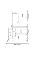
- the organic EL element 1 includes a light-transmitting substrate 2, an anode 3, a cathode 4, and an organic compound layer 10 disposed between the anode 3 and the cathode 4.
- the organic compound layer 10 has a light emitting layer 5 containing a host material and a dopant material.
- the organic compound layer 10 includes a hole injection layer 6 and a hole transport layer 7 in order from the anode 3 between the light emitting layer 5 and the anode 3. Further, the organic compound layer 10 includes an electron transport layer 8 and an electron injection layer 9 in this order from the light emitting layer 5 side between the light emitting layer 5 and the cathode 4.
- the compounds used for the host material and the dopant material are as follows.
- -Host material As a host material, the 1st material represented by following General formula (1) can be used.
- A is a group having a partial structure selected from the following general formulas (a-1) to (a-7); B is a group having a partial structure selected from the following general formulas (b-1) to (b-6); L is a single bond or a linking group.
- the linking group is A substituted or unsubstituted aryl group having 6 to 30 ring carbon atoms, It is a group derived from either a substituted or unsubstituted heterocyclic group having 5 to 30 ring-forming atoms, or a group in which 2 to 5 of these groups are linked to each other.
- the groups connected to each other are the same or different from each other.
- a is an integer of 1 to 5 representing the number of substitutions of A directly bonded to L; When a is 2 or more, the plurality of A are the same or different from each other.
- b is an integer of 1 to 5 representing the number of substitutions of B directly bonded to L; When b is 2 or more, the plurality of B are the same or different from each other.
- R is Hydrogen atom, A substituted or unsubstituted aryl group having 6 to 30 ring carbon atoms, A substituted or unsubstituted heterocyclic group having 5 to 30 ring atoms, or a substituted or unsubstituted alkyl group having 1 to 30 carbon atoms.
- R may couple
- B is a structure having a donor element
- A is a structure having an acceptor element. That is, the partial structure selected from the general formulas (b-1) to (b-6) of B is a structure having a donor element, and the general formulas (a-1) to (a-7) of A have The partial structure selected from is a structure having an acceptor element.
- the donor element refers to electron donating property
- the acceptor element refers to electron accepting property.
- the general formula (1) is preferably any one of the following general formulas (1a) to (1g).
- the aryl group having 6 to 30 ring carbon atoms includes a condensed aryl group, such as a phenyl group, a 1-naphthyl group, 2-naphthyl group, 1-anthryl group, 2-anthryl group, 9-anthryl group, benzanthryl group, 1-phenanthryl group, 2-phenanthryl group, 3-phenanthryl group, 4-phenanthryl group, 9-phenanthryl group, Naphthacenyl group, pyrenyl group, 1-chrysenyl group, 2-chrysenyl group, 3-chrysenyl group, 4-chrysenyl group, 5-chrysenyl group, 6-chrysenyl group, benzo [c] phenanthryl group, benzo [g] chrysenyl group, 1-triphenylenyl group, 2-triphenylenyl group, 3-tri
- the aryl group preferably has 6 to 20 ring carbon atoms, and more preferably 6 to 12 carbon atoms.
- a phenyl group, a biphenyl group, a naphthyl group, a phenanthryl group, and a terphenyl group are particularly preferable.
- heterocyclic group having 5 to 30 ring atoms examples include condensed heterocyclic groups such as pyrrolyl group, pyrazinyl group, pyridinyl group, indolyl group, isoindolyl group, imidazolyl group, furyl group, benzofuranyl group, isobenzo group.
- the number of ring-forming atoms of the heterocyclic group is preferably 5-20, and more preferably 5-14.
- 1-dibenzofuranyl group, 2-dibenzofuranyl group, 3-dibenzofuranyl group, 4-dibenzofuranyl group, 1-dibenzothiophenyl group, 2-dibenzothiophenyl group, 3- A dibenzothiophenyl group, a 4-dibenzothiophenyl group, a 1-carbazolyl group, a 2-carbazolyl group, a 3-carbazolyl group, a 4-carbazolyl group, and a 9-carbazolyl group are preferable.
- the 1-carbazolyl group 2-carbazolyl group, 3-carbazolyl group and 4-carbazolyl group, a substituted or unsubstituted aryl group having 6 to 30 ring carbon atoms or a substituted or unsubstituted group at the 9-position nitrogen atom It is preferable that the heterocyclic group having 5 to 30 ring atoms is substituted.
- the alkyl group having 1 to 30 carbon atoms may be linear, branched or cyclic.
- the linear or branched alkyl group include a methyl group, ethyl group, propyl group, isopropyl group, n-butyl group, s-butyl group, isobutyl group, t-butyl group, n-pentyl group, n- Hexyl, n-heptyl, n-octyl, n-nonyl, n-decyl, n-undecyl, n-dodecyl, n-tridecyl, n-tetradecyl, n-pentadecyl, n- Hexadecyl, n-heptadecyl, n-octadecyl, neopentyl, 1-methylpentyl
- Examples of the cyclic alkyl group include a cyclopropyl group, a cyclobutyl group, a cyclopentyl group, a cyclohexyl group, a 4-methylcyclohexyl group, a 3,5-tetramethylcyclohexyl group, a cycloheptyl group, a cyclooctyl group, Examples include 1-adamantyl group, 2-adamantyl group, 1-norbornyl group, 2-norbornyl group and the like.
- the carbon number of the linear or branched alkyl group is preferably 1 to 10, and more preferably 1 to 6.
- methyl group, ethyl group, propyl group, isopropyl group, n-butyl group, s-butyl group, isobutyl group, t-butyl group, n-pentyl group, n-hexyl group Is preferred.
- the number of carbon atoms forming the ring of the cycloalkyl group is preferably 3 to 10, and more preferably 5 to 8.
- a cyclopentyl group and a cyclohexyl group are preferable.
- halogenated alkyl group in which the alkyl group is substituted with a halogen atom include those in which the alkyl group having 1 to 30 carbon atoms is substituted with one or more halogen groups. Specific examples include a fluoromethyl group, a difluoromethyl group, a trifluoromethyl group, a fluoroethyl group, and a trifluoromethylmethyl group.
- L is preferably a single bond or a divalent group derived from a phenyl group, a biphenyl group, a terphenyl group, or a triphenylenyl group. By setting it as such L, in a compound, it becomes possible to localize so that the electron orbit of LUMO and HOMO may not overlap.
- a and B are condensed as a partial structure in the general formula (1) from the viewpoint of localizing the LUMO and HOMO electron orbits so as not to overlap. It is preferred not to have aromatic hydrocarbons.
- R is a group derived from a substituted or unsubstituted aryl group having 6 to 30 ring carbon atoms, a phenyl group, a biphenyl group, a terphenyl Group and triphenylenyl group are preferable.
- B in the general formula (1) is represented by any one of the following general formulas (2), (3), (4), (5), and (6). preferable.
- R 1 to R 8 are each independently Hydrogen atom, A substituted or unsubstituted aryl group having 6 to 30 ring carbon atoms, A substituted or unsubstituted heterocyclic group having 5 to 30 ring atoms, A substituted or unsubstituted alkyl group having 1 to 30 carbon atoms, A substituted or unsubstituted alkylsilyl group having 3 to 30 carbon atoms, A substituted or unsubstituted arylsilyl group having 6 to 60 ring carbon atoms, A substituted or unsubstituted alkoxy group having 1 to 30 carbon atoms, A substituted or unsubstituted aryloxy group having 6 to 30 ring carbon atoms, A substituted or unsubstituted alkylamino group having 2 to 30 carbon atoms, A substituted or unsubstituted arylamino group having 6 to 60 ring carbon atoms, A substituted or unsubstituted
- L 1 represents any one of the linking groups selected from the following general formulas (21) to (27).
- n1 represents an integer of 1 to 3, when n1 is 2 or 3, a plurality of L 1 are mutually identical or different.
- X 1 represents any one of the linking groups selected from the following general formulas (41) to (45). )
- R 101 has the same meaning as R 1 to R 8 in the general formula (2). However, in the general formula (2), one of R 1 to R 8 or one of R 101 is a single bond bonded to L. When a plurality of R 101 are present, they are the same as or different from each other. )
- R x is Hydrogen atom, A substituted or unsubstituted aryl group having 6 to 30 ring carbon atoms, A substituted or unsubstituted heterocyclic group having 5 to 30 ring atoms, or a substituted or unsubstituted alkyl group having 1 to 30 carbon atoms.
- R x is Hydrogen atom, A substituted or unsubstituted aryl group having 6 to 30 ring carbon atoms, A substituted or unsubstituted heterocyclic group having 5 to 30 ring atoms, or a substituted or unsubstituted alkyl group having 1 to 30 carbon atoms.
- the compound represented by the general formula (2) may be represented by any one of the following general formulas (2a) to (2c).
- R 10 has the same meaning as R 1 to R 8 in the general formula (2).
- m1 and m3 represent integers from 0 to 4, and m2 represents an integer from 0 to 2.
- a plurality of R 10 are each the same or different.
- X 1 represents any one of the linking groups selected from the above formulas (41) to (45). The plurality of X 1 are the same as or different from each other.
- one of R 10 and R x in the above formulas (43) to (45) is a single bond bonded to L.
- R 1 ⁇ R 8, L 1, and n1 have the same meanings as R 1 ⁇ R 8, L 1 , and n1 in the general formula (2).
- R 9 has the same meaning as R 1 to R 8 in the general formula (2).
- R 10 has the same meaning as R 1 to R 8 in the general formula (2).
- m4 and m6 each represents an integer from 0 to 4, and m5 represents an integer from 0 to 2.
- a plurality of R 10 are each the same or different.
- X 1 represents any one of the linking groups selected from the above general formulas (41) to (45). The plurality of X 1 are the same as or different from each other. )
- R 21 to R 24 have the same meanings as R 1 to R 8 in the general formula (2). However, any combination of R 21 and R 22 , R 22 and R 23 , and R 23 and R 24 may form a saturated or unsaturated ring structure.
- X 1 represents any one of the linking groups selected from the above formulas (41) to (45).
- one of R 21 to R 24 and R x is a single bond bonded to L.
- R 25 to R 30 have the same meanings as R 1 to R 8 in the general formula (2). However, any combination of R 25 and R 26 , R 27 and R 28 , R 28 and R 29 , and R 29 and R 30 may form a saturated or unsaturated ring structure.
- X 1 represents any one of the linking groups selected from the above formulas (41) to (45). However, in the general formula (4), one of R 25 to R 30 and R x is a single bond bonded to L.
- R 31 to R 38 have the same meanings as R 1 to R 8 in the general formula (2). However, any combination of R 31 and R 32 , R 32 and R 33 , R 33 and R 34 , R 35 and R 36 , R 36 and R 37 , R 37 and R 38 is a saturated or unsaturated ring structure May be formed.
- X 1 represents any one of the linking groups selected from the above general formulas (41) to (45). However, in the general formula (5), one of R 31 to R 38 and R x is a single bond bonded to L. )
- At least one of R 31 to R 38 in the general formula (5) is preferably represented by the following general formula (51).
- R 39 has the same meaning as R 1 to R 8 in the general formula (2).
- r represents an integer from 0 to 3
- S represents an integer from 0 to 4.
- X 1 represents any one of the linking groups selected from the above general formulas (41) to (45).
- L 61 is a single bond or a linking group.
- the linking group is A substituted or unsubstituted aryl group having 6 to 30 ring carbon atoms, It is a group derived from either a substituted or unsubstituted heterocyclic group having 5 to 30 ring-forming atoms, or a group in which 2 to 5 of these groups are linked to each other.
- the groups connected to each other are the same or different from each other.
- Ar b is a single bond or a substituted or unsubstituted aryl group having 6 to 30 ring carbon atoms.
- Z b is A substituted or unsubstituted tertiary alkyl group having 4 to 30 carbon atoms, A substituted or unsubstituted alkylsilyl group having 3 to 30 carbon atoms, A substituted or unsubstituted arylsilyl group having 6 to 60 ring carbon atoms, A substituted or unsubstituted alkoxy group having 1 to 30 carbon atoms, A substituted or unsubstituted aryloxy group having 6 to 30 ring carbon atoms, A substituted or unsubstituted alkylamino group having 2 to 60 carbon atoms, A substituted or unsubstituted arylamino group having 6 to 60 ring carbon atoms, A substituted or unsubstituted alkylthio group having 1 to 30 carbon atoms,
- examples of the aryl group having 6 to 30 ring carbon atoms and the heterocyclic group having 5 to 30 ring atoms include the above general formulas (1) and ( Examples thereof include the groups described in (b-1) to (b-6).
- examples of the alkyl group having 1 to 30 carbon atoms include the groups described in the general formulas (1) and (b-1) to (b-6). It is done.
- the tertiary alkyl group having 4 to 30 carbon atoms in the general formula (6) is, among the groups described in the general formulas (1) and (b-1) to (b-6), a tertiary alkyl group. Can be mentioned.
- examples of the alkylsilyl group having 3 to 60 carbon atoms include trialkylsilyl groups having an alkyl group exemplified as the alkyl group having 1 to 30 carbon atoms.
- the three alkyl groups may be the same or different from each other.
- Examples of the arylsilyl group having 6 to 60 ring carbon atoms include a dialkylarylsilyl group, an alkyldiarylsilyl group, and a triarylsilyl group.
- Examples of the dialkylarylsilyl group include a dialkylarylsilyl group having two alkyl groups exemplified as the alkyl group having 1 to 30 carbon atoms and one aryl group having 6 to 30 ring carbon atoms. .
- the carbon number of the dialkylarylsilyl group is preferably 8-30.
- the two alkyl groups may be the same or different.
- alkyldiarylsilyl group examples include an alkyldiarylsilyl group having one alkyl group exemplified for the alkyl group having 1 to 30 carbon atoms and two aryl groups having 6 to 30 ring carbon atoms. .
- the alkyldiarylsilyl group preferably has 13 to 30 carbon atoms.
- the two aryl groups may be the same or different.
- Examples of the triarylsilyl group include a triarylsilyl group having three aryl groups having 6 to 30 ring carbon atoms.
- the carbon number of the triarylsilyl group is preferably 18-30.
- the three aryl groups may be the same or different from each other.
- Examples of such an arylsilyl group include a phenyldimethylsilyl group, a diphenylmethylsilyl group, a diphenyl-t-butylsilyl group, and a triphenylsilyl group.
- the alkoxy group having 1 to 30 carbon atoms is represented by —OR V.
- RV include the alkyl group having 1 to 30 carbon atoms.
- the alkoxy group is preferably an alkoxy group having 1 to 6 carbon atoms, and examples thereof include a methoxy group, an ethoxy group, a propoxy group, a butoxy group, a pentyloxy group, and a hexyloxy group.
- Examples of the halogenated alkoxy group in which the alkoxy group is substituted with a halogen atom include those in which the alkoxy group having 1 to 30 carbon atoms is substituted with one or more halogen groups.
- An aryloxy group having 6 to 30 ring carbon atoms is represented by —OR W.
- R W an aryl group the ring-forming carbon atoms 6 to 30.
- the aryloxy group include a phenoxy group.
- the alkylamino group having 2 to 60 carbon atoms is represented as —NHR V or —N (R V ) 2 .
- RV include the alkyl group having 1 to 30 carbon atoms.
- the arylamino group having 6 to 60 ring carbon atoms is represented by —NH 2 R W or —NH (R W ) 2 . Examples of R W, and an aryl group the ring-forming carbon atoms 6 to 30.
- the alkylthio group having 1 to 30 carbon atoms is represented as —SR V.
- RV include the alkyl group having 1 to 30 carbon atoms.
- An arylthio group having 6 to 30 ring carbon atoms is represented by —SR W.
- R W, and an aryl group the ring-forming carbon atoms 6 to 30.
- R 31 to R 38 are a substituted or unsubstituted aryl group having 6 to 30 ring carbon atoms
- Ar b and R W are LUMO and HOMO in the compound represented by the general formula (1).
- a phenyl group, a biphenyl group, a terphenyl group, and a triphenylenyl group are preferable.
- R 10 has the same meaning as R 1 to R 8 in the general formula (2).
- m7 and m8 represent an integer of 0 to 4.
- a plurality of R 10 are each the same or different.
- X 1 represents any one of the linking groups selected from the above formulas (41) to (45). The plurality of X 1 are the same as or different from each other. )
- a in the general formula (1) is any of the following general formulas (8), (9), (10), (11), (12), (13), and (14). It is preferable that
- each R y is independently Hydrogen atom, Fluorine atom, A cyano group, Nitro group, A substituted or unsubstituted aryl group having 6 to 30 ring carbon atoms, A substituted or unsubstituted heterocyclic group having 5 to 30 ring atoms, A substituted or unsubstituted alkyl group having 1 to 30 carbon atoms, A substituted or unsubstituted alkylcarbonyl group having 1 to 30 carbon atoms, A substituted or unsubstituted arylcarbonyl group having 6 to 30 ring carbon atoms, A substituted or unsubstituted alkylsulfinyl group having 1 to 30 carbon atoms, A substituted or unsubstituted
- Y 3 is synonymous with the other Y 1 in the general formula (8).
- X 3 represents any one of the linking groups selected from the following general formulas (41) to (45). )
- Each R x is independently Hydrogen atom, A substituted or unsubstituted aryl group having 6 to 30 carbon atoms, A substituted or unsubstituted heterocyclic group having 5 to 30 ring atoms or a substituted or unsubstituted alkyl group having 1 to 30 carbon atoms. When a plurality of R x are present, they are the same or different from each other. )
- R 41 to R 48 is a single bond bonded to L, Other R 41 to R 48 have the same meaning as R y in the general formula (8).
- L 4 represents any one of the linking groups selected from the following general formulas (131) to (136).
- p represents an integer of 1 to 3, and when p is 2 or 3, the plurality of L 4 are the same or different from each other.
- Each R 301 is independently Hydrogen atom, A substituted or unsubstituted aryl group having 6 to 30 ring carbon atoms, A substituted or unsubstituted heterocyclic group having 5 to 30 ring atoms, or a substituted or unsubstituted alkyl group having 1 to 30 carbon atoms. When a plurality of R 301 are present, they are the same or different from each other. )
- Ar a is A substituted or unsubstituted aryl group having 6 to 30 ring carbon atoms, or A substituted or unsubstituted heterocyclic group having 5 to 30 ring atoms.
- Z a is Fluorine atom, A cyano group, Nitro group, A substituted or unsubstituted alkylcarbonyl group having 1 to 20 carbon atoms, A substituted or unsubstituted arylcarbonyl group having 6 to 30 ring carbon atoms, A substituted or unsubstituted alkylsulfinyl group having 1 to 20 carbon atoms, A substituted or unsubstituted arylsulfinyl group having 6 to 30 ring carbon atoms, A substituted or unsubstituted alkylphosphinyl group having 2 to 60 carbon atoms, A substituted or unsubstituted arylphosphinyl group having 6 to 60 ring carbon atoms, A substituted or unsubsti
- an aryl group having 6 to 30 ring carbon atoms, a heterocyclic group having 5 to 30 ring atoms, an alkyl group having 1 to 30 carbon atoms, and an alkyl group having 3 to 60 carbon atoms examples include the above general formulas (1) and (b -1) to (b-2) and the groups described in the general formulas (2) to (6).
- An alkylcarbonyl group having 1 to 30 carbon atoms is represented by —COOR V.
- An arylcarbonyl group having 6 to 30 ring carbon atoms is represented by —COOR W.
- the alkylsulfinyl group having 1 to 30 carbon atoms is represented as —S ( ⁇ O) R V.
- the alkylphosphinyl group having 2 to 40 carbon atoms is represented by —P ( ⁇ O) HR V or —P ( ⁇ O) (R V ) 2 .
- the arylphosphinyl group having 6 to 30 ring carbon atoms is represented by —P ( ⁇ O) HR W or —P ( ⁇ O) (R W ) 2 .
- the alkylsulfonyl group having 1 to 30 carbon atoms is represented by —S ( ⁇ O) 2 R V.
- examples of R V include the above alkyl groups having 1 to 30 carbon atoms.
- R W is an aryl group of the ring carbon atoms 6 to 30.
- the aryl group having 6 to 30 ring carbon atoms is preferably a phenyl group, a biphenyl group, a terphenyl group, or a triphenylenyl group.
- the first material represented by the general formula (1) is preferably a biscarbazole derivative represented by the following general formula (101) from the viewpoint of forming a compound in which a donor element and an acceptor element are bonded in the molecule.
- a 1 and A 2 are independently of each other, Hydrogen atom, A halogen atom, A cyano group, A substituted or unsubstituted aryl group having 6 to 30 ring carbon atoms, A substituted or unsubstituted heterocyclic group having 5 to 30 ring atoms, A substituted or unsubstituted alkyl group having 1 to 30 carbon atoms, A substituted or unsubstituted alkoxy group having 1 to 30 carbon atoms, A substituted or unsubstituted aralkyl group having 7 to 30 carbon atoms, A substituted or unsubstituted aryloxy group having 6 to 30 ring carbon atoms, It represents a substituted or unsubstituted alkylsilyl group having 3 to 60 carbon atoms, or a substituted or unsubstituted arylsilyl group having 8 to 30 ring carbon atoms. However, it is preferable that at least one of A 1 and
- Y 11 to Y 14 and Y 23 to Y 26 each independently represent C (R) or a nitrogen atom
- Y 15 to Y 18 each independently represent C ( R)
- Y 19 ⁇ Y 22 are independently of each other, combined with either C (R), a nitrogen atom or Y 15 ⁇ Y 18 R represents a hydrogen atom or a substituent each independently.
- the substituent in R is synonymous with the substituent when A 1 and A 2 described above have a substituent.
- L 1 and L 2 are each independently a single bond, a substituted or unsubstituted divalent aromatic hydrocarbon group having 6 to 30 ring carbon atoms, a substituted or unsubstituted group. It represents a divalent heterocyclic group having 5 to 30 ring atoms, or a group in which the divalent aromatic hydrocarbon group and the divalent heterocyclic group are linked.
- At least one of the L 1 and the L 2 is preferably represented by the following general formula (a).
- Y 31 to Y 35 each independently represent C (R a ), a nitrogen atom or a carbon atom bonded to L 3 ;
- Each R a independently represents a hydrogen atom or a substituent.
- the substituent in R a has the same meaning as the substituent when A 1 and A 2 described above have a substituent.
- L 3 and L 4 are each independently a single bond, A substituted or unsubstituted divalent aromatic hydrocarbon group having 6 to 30 ring carbon atoms, It represents a substituted or unsubstituted divalent heterocyclic group having 5 to 30 ring atoms, or a group in which the divalent aromatic hydrocarbon group and the divalent heterocyclic group are linked.
- Examples of the aryloxy group having 6 to 30 ring carbon atoms, the alkylsilyl group having 3 to 60 carbon atoms, and the arylsilyl group having 8 to 30 ring carbon atoms include the general formulas (1) and (b-1) described above. ) To (b-2) and the groups described in the general formulas (2) to (6).
- examples of the aralkyl group having 7 to 30 carbon atoms include the groups described in the aralkyl group having 7 to 30 carbon atoms in the general formula (20) described later.
- examples of the divalent aromatic hydrocarbon group include divalent groups derived from the aryl groups in the general formulas (1) and (b-1) to (b-6). It is done.
- examples of the divalent heterocyclic group having 5 to 30 ring atoms include the heterocyclic groups in the general formulas (1) and (b-1) to (b-6). Examples thereof include a divalent group to be derived.
- A is represented by the general formula (14)
- B is represented by the general formula (2)
- L is a substituted or unsubstituted ring-forming carbon. Those having an aryl group of 6 to 30 are preferred. Further, L is preferably a phenylene group.
- ring-forming carbon means a carbon atom constituting a saturated ring, an unsaturated ring, or an aromatic ring.
- Ring-forming atom means a carbon atom and a hetero atom constituting a hetero ring (including a saturated ring, an unsaturated ring, and an aromatic ring).
- examples of the substituent include an aryl group, a heterocyclic group, an alkyl group (a linear or branched alkyl group, a cycloalkyl group, a halogenated alkyl group) as described above,
- alkenyl groups, alkynyl groups, alkylsilyl groups, arylsilyl groups, alkoxy groups, halogenated alkoxy groups, aralkyl groups, aryloxy groups, halogen atoms, cyano groups, hydroxyl groups, nitro groups, carboxy groups, and the like can be given.
- an aryl group, a heterocyclic group, an alkyl group, a halogen atom, an alkylsilyl group, an arylsilyl group, and a cyano group are preferable, and further, specific examples that are preferable in the description of each substituent Are preferred.
- the term “unsubstituted” in the case of “substituted or unsubstituted” means that a hydrogen atom is bonded without being substituted with the substituent.
- the hydrogen atom includes isotopes having different numbers of neutrons, that is, light hydrogen (Protium), deuterium (Deuterium), and tritium (Tritium).
- a fluorescent material dopant material is used for the dopant material of a light emitting layer.
- a known fluorescent material can be used as the fluorescent material.
- bisarylaminonaphthalene derivatives, aryl-substituted naphthalene derivatives, bisarylaminoanthracene derivatives, aryl group-substituted anthracene derivatives, bisarylaminopyrene derivatives, aryl group-substituted pyrene derivatives, bisarylaminochrysene derivatives, aryl-substituted Examples include chrysene derivatives, bisarylaminofluoranthene derivatives, aryl-substituted fluoranthene derivatives, indenoperylene derivatives, pyromethene boron complex compounds, compounds having a pyromethene skeleton or metal complexes thereof, dike
- a dopant material represented by the following general formula (20) is particularly preferable.
- Ar 0 is a substituted or unsubstituted divalent condensed aromatic hydrocarbon group having 10 to 50 ring carbon atoms
- Ar 1 to Ar 4 are each independently A substituted or unsubstituted aryl group having 6 to 30 ring carbon atoms, A substituted or unsubstituted heterocyclic group having 5 to 30 ring atoms, A substituted or unsubstituted alkyl group having 6 to 30 carbon atoms, or A substituted or unsubstituted aralkyl group having 7 to 50 carbon atoms.
- Examples of the divalent condensed aromatic hydrocarbon group having 10 to 50 ring carbon atoms in the general formula (20) include naphthylene group, anthracenylene group, phenanthrylene group, chrysenylene group, pyrenylene group, benzoanthracenylene group, fluoranthate.
- Nylene group benzofluoranthenylene group, peryleneylene group, coronerylene group, picenylene group, diphenylanthracenylene group, fluorenylene group, triphenylylene group, rubisenylene group, phenylanthracenylene group, bisanthracenylene group, dianthracenylbenzylinylene Group, dibenzoanthracenylene group and the like, and naphthylene group, anthracenylene group, phenanthrylene group, chrysenylene group, pyrenylene group and benzoanthracenylene group are preferable.
- the above general formulas (1) and (b- Examples thereof include the groups described in 1) to (b-6).
- the aralkyl group having 7 to 30 carbon atoms in the general formula (20) is represented by -Rv-Rw.
- Rv include an alkylene group corresponding to the alkyl group having 1 to 30 carbon atoms.
- this Rw include the examples of the aryl group having 6 to 30 ring carbon atoms.
- the aralkyl group has an aralkyl group having 7 to 30 carbon atoms (the aryl moiety has 6 to 30 carbon atoms, preferably 6 to 20 carbon atoms, more preferably 6 to 12 carbon atoms), and the alkyl moiety has 1 to 30 carbon atoms (preferably 1 to 20 carbon atoms). More preferably, it is 1 to 10, and more preferably 1 to 6).
- Examples of the aralkyl group include benzyl group, 2-phenylpropan-2-yl group, 1-phenylethyl group, 2-phenylethyl group, 1-phenylisopropyl group, 2-phenylisopropyl group, and phenyl-t-butyl.
- ⁇ -naphthylmethyl group 1- ⁇ -naphthylethyl group, 2- ⁇ -naphthylethyl group, 1- ⁇ -naphthylisopropyl group, 2- ⁇ -naphthylisopropyl group, ⁇ -naphthylmethyl group, 1- ⁇ - Naphthylethyl group, 2- ⁇ -naphthylethyl group, 1- ⁇ -naphthylisopropyl group, 2- ⁇ -naphthylisopropyl group, 1-pyrrolylmethyl group, 2- (1-pyrrolyl) ethyl group, p-methylbenzyl group, m -Methylbenzyl group, o-methylbenzyl group, p-chlorobenzyl group, m-chlorobenzyl group, o-chlorobenzyl group, p-bromine Benzyl group, m
- At least one of Ar 1 to Ar 4 in the general formula (20) is preferably represented by the following general formula (21).
- n is an integer from 0 to 3
- m is an integer from 0 to 5
- l is an integer from 0 to 7.
- X is an oxygen atom, a sulfur atom or a selenium atom
- Ar represents a substituted or unsubstituted arylene group having 6 to 30 ring carbon atoms
- R is A halogen atom, A cyano group, Nitro group, Hydroxyl group, Silyl group, Carboxyl group, A substituted or unsubstituted aryl group having 6 to 30 ring carbon atoms, A substituted or unsubstituted alkyl group having 1 to 30 carbon atoms, A substituted or unsubstituted alkylamino group having 1 to 30 carbon atoms, A substituted or unsubstituted arylamino group having 6 to 60 ring carbon atoms, a substituted or unsubstituted alkoxy group having 1 to 30 carbon atoms, A substituted or unsubstit
- the plurality of Ar and R are the same or different. When there are a plurality of R, they may be bonded to each other to form a saturated or unsaturated, optionally substituted 5-membered or 6-membered cyclic structure.
- an aryl group having 6 to 30 ring carbon atoms an alkyl group having 1 to 30 carbon atoms, an alkylamino group having 1 to 30 carbon atoms, an arylamino group having 6 to 60 ring carbon atoms
- Examples of the alkoxy group having 1 to 30 carbon atoms, the aryloxy group having 6 to 30 ring carbon atoms, and the arylthio group having 6 to 30 ring carbon atoms include the general formulas (2) to (6) and (51) described above. And the groups described in the above.
- the alkoxycarbonyl group having 1 to 30 carbon atoms is represented as —COOR V, and examples of the R V include those similar to the alkyl group having 1 to 30 carbon atoms.
- the film thickness of the light emitting layer is preferably 5 nm to 50 nm, more preferably 7 nm to 50 nm, and most preferably 10 nm to 50 nm. If the thickness is less than 5 nm, it is difficult to form a light emitting layer and the adjustment of chromaticity may be difficult, and if it exceeds 50 nm, the driving voltage may increase.
- the mass ratio of the host material to the fluorescent light emitting dopant material is preferably 99: 1 or more and 50:50 or less.
- the host material and dopant material described above are preferably compounds that satisfy the following specific conditions. This specific condition will be described next.
- the singlet energy EgS (H) of the host material and the singlet energy EgS (D) of the dopant material satisfy the relationship of the following formula (1), and the host material has a singlet energy EgS (H) of 77 [K It is preferable that the difference ⁇ ST (H) with respect to the energy gap Eg 77K (H) satisfies the relationship of the following mathematical formula (2).
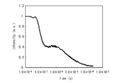
- Eg 77K is a measured value, and a phosphorescence spectrum (vertical axis: phosphorescence emission intensity, horizontal axis: wavelength) of a sample of a luminescent material is measured at a low temperature (77 [K]).
- An energy gap is an energy amount calculated from a predetermined conversion formula based on the wavelength value of the intersection of the tangent and the horizontal axis with respect to the short wavelength rising edge.
- the difference ⁇ T between the energy gap Eg 77K (H) at 77 [K] of the host material and the energy gap Eg 77K (T) at 77 [K] of the dopant material satisfies the relationship of the following formula (3). Is preferred.
- ⁇ ST a compound having a small energy difference ( ⁇ ST) between singlet energy EgS and triplet energy EgT
- the organic EL element emits light with high efficiency in a high current density region.
- the above ⁇ ST (H) represents ⁇ ST of the host material.
- quantum exchange is realized by a small exchange interaction between the singlet energy EgS and the triplet energy EgT.
- a compound having ⁇ ST of 0 eV or more and less than 0.3 eV can be mentioned.
- a more preferable compound is a compound that forms an aggregate in which dipoles formed in an excited state of a molecule interact with each other and exchange exchange energy becomes small. According to the study by the present inventors, such a compound has approximately the same dipole direction, and ⁇ ST can be further reduced by molecular interaction. In such a case, ⁇ ST can be extremely small, from 0 eV to 0.2 eV.
- the energy difference ( ⁇ ST) between the singlet energy EgS and the triplet energy EgT can be reduced by forming an aggregate.
- the aggregate here does not reflect a simple electronic state of only one molecule, but a few molecules are physically close to each other.
- the electronic state between the plurality of molecules is mixed, the energy level changes due to the change of the electronic state, and the value of singlet energy mainly decreases, thereby reducing the value of ⁇ ST. It is considered to be.
- Such a decrease in the value of ⁇ ST due to the formation of aggregates can also be explained by a Davydov splitting model in which the electronic state changes as two molecules approach (see FIG. 2).
- the relationship between the half-value width of the photoluminescence spectrum and the ease of formation of the aggregate can be estimated as follows.
- the vibration level in the excited singlet state is small, and as a result, the half width of the photoluminescence spectrum is observed to be narrow.
- CBP 4,4′-bis [9-dicarbazolyl] -2,2′-biphenyl
- the half-value width of the photoluminescence spectrum is about 50 nm. And relatively narrow.
- association body in this embodiment means that single molecules form arbitrary association bodies. That is, it does not indicate a specific meeting state.
- the association state of organic molecules allows a variety of states in the thin film to be stochastically different from that of inorganic molecules.
- ⁇ TADF mechanism As described above, when ⁇ ST (H) of an organic material is small, the reverse intersystem crossing from the triplet level of the host material to the singlet level of the host material is likely to occur due to externally applied thermal energy. Become.
- an energy state conversion mechanism in which the excited triplet state of the electrically excited exciton inside the organic EL element is spin-exchanged to the excited singlet state by the inverse intersystem crossing is called a TADF mechanism.
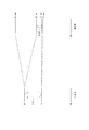
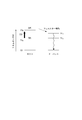
- a compound having a small ⁇ ST (H) is used for the host material, reverse intersystem crossing from the triplet level of the host material to the singlet level of the host material occurs due to externally applied thermal energy. Make it easier. FIG.
- S0 represents the ground state
- S1 H represents the lowest excited singlet state of the host material
- T1 H represents the lowest excited triplet state of the host material
- S1 D represents the lowest of the dopant material. It represents an excited singlet state
- T1 D represents the lowest excited triplet state of the dopant material.
- the difference between the S1 H and T1 H corresponds to .DELTA.St (H)
- the difference between the S1 H and S0 correspond to EGS (H)
- the difference between the S1 D and S0 is EGS ( D)
- the difference between T1 H and T1 D corresponds to ⁇ T.
- the dashed arrows in FIG. 3 represent the energy transfer between each excited state.
- a compound having a small ⁇ ST (H) is selected as a compound used for the host material of the present embodiment. This is because in a material having a small ⁇ ST (H), a triplet exciton generated in the lowest excited triplet state T1 H crosses back to the lowest excited singlet state S1 H of the host material due to thermal energy. This is because it is considered easy. Since ⁇ ST (H) is small, for example, crossing between inverse terms easily occurs even at about room temperature.
- the rate of energy transfer due to Forster transfer from the host material to the lowest excited singlet state T1 D of the fluorescent material dopant material also increases, and as a result, the fluorescent organic EL
- the luminous efficiency of the device is improved. That is, by using a compound having a small ⁇ ST (H) as the host material, light emission derived from the TADF mechanism increases, and as a result, the delayed fluorescence ratio increases. If the delayed fluorescence ratio is increased, a high internal quantum efficiency can be obtained. Note that it is theoretically possible to increase the internal quantum efficiency to 100% by utilizing delayed fluorescence by this TADF mechanism.
- FIG. 4 shows the relationship between the energy levels of the host material and the dopant material of the light emitting layer in the TADF mechanism described in Patent Document 1.
- S0, S1 H, T1 H, S1 D, T1 D has the same meaning as in FIG. 3, dashed arrows represent energy transfer between the excited state.
- a material having a small ⁇ ST (D) is used as a dopant material.
- the lowest excited triplet state T1 D of the dopant material can cross back to the lowest excited singlet state S1 D by thermal energy, and as a result, from the lowest excited singlet state T1 D of the dopant material. Fluorescence emission can be observed. It is thought that the internal efficiency can theoretically be increased to 100% also by utilizing delayed fluorescence by this TADF mechanism.
- Non-Patent Document 1 a fluorescent compound having a small ⁇ ST (H) as described in Non-Patent Document 1 as a host material in the host-dopant system. The reason is as described in detail below.
- the dopant material when considering the energy state conversion by the TADF mechanism on the dopant material, the dopant material emits fluorescence, and therefore has a relatively high singlet energy and a comparable triplet energy. Become. In order to effectively confine the triplet energy in the light emitting layer, it is necessary to select a host material having a larger triplet energy.
- the singlet energy of the host material that is, the energy difference between the HOMO level and the LUMO level becomes very large. .
- the inventors of the present invention preferably convert the energy state by the TADF mechanism on the host material, which makes carrier injection into the light emitting layer advantageous and facilitates carrier balance as a whole of the organic EL element. Think.
- triplet-triplet-annihilation means that triplet excitons generated on a molecule having a long exciton lifetime are adjacent to each other at high density, and excitons collide with each other. Is a physical phenomenon that causes heat inactivation.
- the present inventors believe that in a host-dopant system in which the triplet energy is unlikely to transition from the host material to the dopant material, a decrease in light emission efficiency in the high current density region can be suppressed to some extent.
- a compound having a small ⁇ ST is used as the host material of the light-emitting layer, and the triplet excitation level of the host material is singlet excitation of the dopant material after crossing back to the singlet excitation level by the TADF mechanism. Energy is transferred to the level. Therefore, the triplet exciton generated is maintained in the triplet excited state on the host material having a large abundance ratio in the light emitting layer.
- the triplet excitons generated are maintained in a triplet excited state on the dopant material having a very small abundance ratio in the light emitting layer. That is, in driving an organic EL element in a high current region, it is preferable to design a system in which triplet excited states are not concentrated on the dopant material.
- a compound having a small ⁇ ST (H) is used as the host material. Adopt as.
- a material having a high emission quantum yield can be easily selected as a dopant material by adopting, as a host material, a material that causes reverse intersystem crossing from a triplet level to a singlet level.
- the singlet excitons whose energy has been transferred to the dopant material quickly relax the light emission, so that it is possible to suppress energy quenching in a high current density region.
- the host material has a carrier transport function and an exciton generation function
- the dopant material has a light emission function.
- This function separates the carrier transport function and the light emitting function in the light emitting layer, and promotes effective organic EL light emission by doping the light emitting layer with a small amount of a dopant material having a high light emission quantum yield. is there.
- a function that causes reverse intersystem crossing by the TADF mechanism is required.
- the inventors have increased the selectivity of a dopant material having a high emission quantum yield that greatly contributes to the light emission efficiency of the organic EL element by requiring the host material to have a function that causes reverse intersystem crossing by the TADF mechanism. . Thereby, it is possible to select a fluorescent light-emitting dopant material that is conventionally known as high efficiency.
- triplet energy is obtained by measuring a phosphorescence spectrum (vertical axis: phosphorescence emission intensity, horizontal axis: wavelength) of a sample in which a compound to be measured is dissolved in a solvent at a low temperature (77 [K]).
- a tangent line is drawn with respect to the rising edge of the phosphorescence spectrum on the short wavelength side, and is calculated from a predetermined conversion formula based on the wavelength value at the intersection of the tangent line and the horizontal axis.
- the compound used for the host material of the present invention has a small ⁇ ST as described above.
- ⁇ ST is small, intersystem crossing and reverse intersystem crossing easily occur even in a low temperature (77 [K]) state, and an excited singlet state and an excited triplet state coexist.
- the spectrum measured in the same manner as described above includes light emission from both the excited singlet state and the excited triplet state, and it is difficult to distinguish from which state the light is emitted.
- the triplet energy EgT described above is measured by the following two measurement methods in order to distinguish the triplet energy EgT from the normal triplet energy EgT in terms of its strict meaning.
- EgT of measurement method 1 A phosphorescence spectrum (vertical axis: phosphorescence emission intensity, horizontal axis: wavelength) is measured at a low temperature (77 [K]) for a sample in which a compound to be measured is dissolved in a solvent, and the short wavelength side of this phosphorescence spectrum.
- a tangent line is drawn with respect to the rising edge of the line, and an energy amount calculated from a predetermined conversion formula based on the wavelength value at the intersection of the tangent line and the horizontal axis is defined as an energy gap Eg 77K .
- ⁇ ST is defined as the difference between the singlet energy EgS of measurement method 1 described later and the energy gap Eg 77K of measurement method 1 described later. Therefore, it is preferable that ⁇ ST (H) is expressed as the above formula (2).
- EgT of measurement method 2 A compound to be measured is deposited on a quartz substrate to prepare a sample, and the film thickness is set to 100 nm. With respect to this sample, a phosphorescence spectrum (vertical axis: phosphorescence emission intensity, horizontal axis: wavelength) is measured at a low temperature (77 [K]), and a tangent line is drawn with respect to the rising edge of the phosphorescence spectrum on the short wavelength side. Based on the wavelength value of the intersection of the tangent and the horizontal axis, the energy amount calculated from a predetermined conversion formula is defined as an energy gap Eg 77K . ⁇ ST is defined as the difference between the singlet energy EgS of the measuring method 2 described later and the energy gap Eg 77K of the measuring method 2. Therefore, it is preferable that ⁇ ST (H) is expressed as the above formula (2).
- the triplet energy may contain an error due to the interaction between the target molecule and the solvent. Therefore, as an ideal condition, measurement in a thin film state is desired in order to eliminate the interaction between the target molecule and the solvent.
- the molecule of the compound used for the host material in the present invention shows a photoluminescence spectrum having a wide half-value width in the solution state, which strongly suggests that an association state is formed even in the solution state. It is considered that the conditions are equivalent.
- normal triplet energy EgT is measured in a solution state. Therefore, in the present invention, for triplet energy Eg 77K , the value measured under the solution condition is used for comparison with the value measured under the thin film condition.
- the singlet energy EgS is also defined in the present invention as calculated in the same manner as a normal method. As the definition of the singlet energy EgS, the following two were used. [2-1] EgS of measurement method 3 A sample to be measured is deposited on a quartz substrate to prepare a sample, and the absorption spectrum (vertical axis: absorbance, horizontal axis: wavelength) of this sample is measured at room temperature (300 K). A tangent line is drawn with respect to the fall of the absorption spectrum on the long wavelength side, and is calculated from a predetermined conversion formula based on the wavelength value at the intersection of the tangent line and the horizontal axis.
- EgS of measurement method 4 A sample to be measured is deposited on a quartz substrate to prepare a sample, and the emission spectrum (vertical axis: emission intensity, horizontal axis: wavelength) of this sample is measured at room temperature (300 K). A tangent line is drawn with respect to the rising edge of the emission spectrum on the short wavelength side, and is calculated from a predetermined conversion formula based on the wavelength value at the intersection of the tangent line and the horizontal axis. Note that EgS in the case of forming an aggregate is determined by the above Davydov in both of the above measurement methods 3 and 4. This corresponds to the energy gap between S1-m- and the ground state S0 in the splitting model.
- the singlet energy EgS and the energy gap Eg 77K there are two definitions of the energy gap Eg 77K and the singlet energy EgS, respectively. From these Eg 77K and EgS, two kinds of ⁇ ST are defined. That is, the ⁇ ST defined by one massive energy EgS energy gap Eg 77K and measuring method 3 of the measuring method 1, there is ⁇ ST defined by singlet energy EgS the energy gap Eg 77K measurement method 2 Measurement method 4 To do.
- ⁇ ST in at least one of the definitions is preferably represented by the above formula (2).
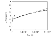
- the delayed fluorescence ratio exceeds the upper limit of the theoretical value of the delayed fluorescence ratio (TTF ratio) when it is assumed that delayed fluorescence occurs only by the TTF mechanism. I found. That is, according to the present invention, an organic EL element with higher internal quantum efficiency can be realized.
- the delayed fluorescence ratio can be measured by a transient EL method.
- the transient EL method is a method of measuring the decay behavior (transient characteristic) of EL light emission after removing the pulse voltage applied to the element.
- the EL emission intensity is classified into a light emission component from a singlet exciton generated by the first recombination and a light emission component from a singlet exciton generated via a triplet exciton.
- the lifetime of singlet excitons generated by the first recombination is on the order of nanoseconds and is very short, and therefore decays quickly after removal of the pulse voltage.
- delayed fluorescence is slowly attenuated due to light emission from singlet excitons generated via long-lived triplet excitons.
- the emission from the singlet exciton generated by the first recombination and the emission from the singlet exciton generated via the triplet exciton are greatly different in time, so the emission from delayed fluorescence
- the strength can be determined. Specifically, it can be determined by the following method.
- the transient EL waveform is measured as follows (see Fig. 5).
- a pulse voltage waveform output from the voltage pulse generator (PG) 11 is applied to the organic EL element (EL) 12.
- the applied voltage waveform is taken into the oscilloscope (OSC) 13.
- OSC oscilloscope
- PMT photomultiplier tube
- the voltage waveform and pulse emission are synchronized and taken into the personal computer (PC) 15.
- the emission intensity ratio derived from delayed fluorescence is defined as follows.
- the TTF ratio calculation formula described in International Publication No. 2010/134352 can be used.
- the delayed fluorescence component defined in the present invention is considered to include the delayed fluorescence due to thermal activation (TADF mechanism) disclosed in the present invention in addition to the TTF-derived luminescent component. Therefore, in the present invention, the ratio of the delayed fluorescence component obtained from the following formula (4) is not called the TTF ratio but is called the delayed fluorescence ratio.
- the delayed fluorescence ratio is obtained using Equation (4).
- the graph of FIG. 6A is a measurement example of a transient EL waveform when a predetermined pulse voltage is applied to the organic EL element and then the voltage is removed, and shows a change with time of the emission intensity of the organic EL element.
- the pulse voltage was removed at about 3 ⁇ 10 ⁇ 8 seconds.
- the graph of FIG. 6A represents the luminance when the voltage is removed as 1.
- the graph of FIG. 6B is a graph in which the reciprocal of the square root of the light intensity up to 1.5 ⁇ 10 ⁇ 5 seconds after the voltage removal is plotted with the voltage removal time point as the origin.
- the emission intensity derived from delayed fluorescence obtained from the transient EL waveform varies depending on the temperature to be measured. Such a phenomenon is considered to be peculiar to fluorescence emission mainly by the TADF mechanism.
- the fitting to a straight line is preferably performed by the least square method. In this case, the fitting is preferably performed using a value up to 10 ⁇ 5 seconds.
- FIG. 7 shows the relationship between the energy levels of the host material and the dopant material in the organic EL element using the TTF mechanism.
- S0, S1 H, T1 H, S1 D, T1 D has the same meaning as in FIG.
- the arrows represent energy transfer between each excited state.
- the TTF mechanism uses a phenomenon in which singlet excitons are generated by collision of two triplet excitons.
- the lowest excited triplet state T1 H of the host material is preferably smaller than the lowest excited triplet state T1 D of the dopant material.
- the triplet exciton is present on the host material molecule. Concentrate on. As the density of these triplet excitons increases, the triplet excitons efficiently cause pair collisions, and part of them change to singlet excitons.
- the lowest excited singlet state S1 H of the host material generated by the TTF mechanism quickly causes Forster transfer to the lowest excited singlet state S1 D of the dopant material, and the dopant material emits fluorescence.
- the upper limit of the theoretical value of the TTF ratio can be obtained as follows. According to SMBachilo et al. (J.Phys.Cem.A, 104,7711 (2000)) , 3 A * ) increases, and triplet excitons collide with each other to cause a reaction such as the following formula (5).
- 1 A represents the ground state
- 1 A * represents the lowest excited singlet exciton.
- TTF ratio TTF-derived emission ratio
- the residual intensity at 1 ⁇ s can be measured.
- the residual intensity ratio at 1 ⁇ s is defined as the ratio of the emission intensity after the elapse of 1 ⁇ s after removing the pulse voltage to the emission intensity at the time when the pulse voltage measured by the transient EL method is removed.
- the amount of relative delayed fluorescence can be estimated from the decay behavior of the EL emission after removing the pulse voltage measured by the transient EL method.
- the residual intensity ratio at 1 ⁇ s can be obtained by reading the emission intensity at 1.0 ⁇ s in the graph of FIG. 6A.
- the residual strength ratio at 1 ⁇ s is preferably larger than 36.0%. More preferably, it is 38.0% or more.
- the preferable dopant material in this embodiment is a fluorescent substance and has a large rate constant of a radiative transition.
- singlet excitons electrically excited by the host material, singlet excitons generated by the TADF mechanism, etc. transfer Forster energy to the singlet excitons of the dopant material, and the dopant material quickly Emits light. That is, before triplet excitons on the host material cause TTA, fluorescence can be emitted through the energy transition, and the efficiency reduction in the high current region may be greatly improved.
- the dopant material having a large rate of radiation transition it is preferable to select a dopant material having a fluorescence lifetime of 5 ns or less. More preferably, it is 2 ns or less. Moreover, it is preferable that the fluorescence quantum yield of dopant material is 80% or more in a solution state. Fluorescence quantum yield, for example, Hamamatsu Photonics Co., absolute using a PL quantum yield measurement apparatus C9920-02, a range of concentrations 10 -5 mol / l ⁇ 10 -6 mol / l toluene solution It can be determined by measuring. In addition, since the dopant material has a large rate constant of radiation transition, the EL spectrum of the device is measured, and it is confirmed that the other light emitting components are 1/10 or less of the light emitting components of the dopant material. Is also estimated.
- IP HT 5.7 eV. This makes it possible to further balance the electron and hole.
- the ionization potential can be obtained, for example, by measuring in a thin film state of the material using a photoelectron spectrometer (manufactured by Riken Keiki Co., Ltd .: AC-3).
- the dopant material is a fluorescent light-emitting dopant material
- the compound used for the host material and the compound used for the dopant material are expressed by the formula (2). Satisfying the singlet energy magnitude relationship. By satisfying such a relationship, the singlet excitons initially generated in the host material and the singlet excitons derived from delayed fluorescence easily transfer to the dopant material. As a result, the dopant material efficiently emits fluorescence.
- ⁇ n is a refractive index n Z perpendicular to the silicon substrate surface in a region where the reflectance observed simultaneously with the refractive index in spectroscopic ellipsometry measurement (measurement range: 200 nm to 1000 nm) is not observed.
- the value when the difference from the refractive index n X in the direction parallel to the silicon substrate is the largest is taken.
- the relationship between the magnitude of ⁇ n and the ease of forming aggregates is presumed as follows.
- the compound used for the host material of the present invention is a compound having ⁇ n of a predetermined size, and it is presumed that it forms an aggregate in a thin film state and has a certain degree of regularity.
- compounds having a very small ⁇ n such as CBP and Alq 3 (tris (8-hydroxyquinolinato) aluminum), exist in an amorphous state in which the molecules have no regularity in a thin film state.
- ⁇ n can be calculated based on the refractive index of each compound measured by spectroscopic ellipsometry.
- Spectral ellipsometry is a method for measuring the optical constant (refractive index n and extinction coefficient k) and film thickness of a thin film.
- a multi-angle high-speed spectroscopic ellipsometer manufactured by JA Woollam, M-2000D.
- FIG. 8A shows an incident angle of incident light from a light source
- FIG. 8B shows a cross-sectional view of an organic thin film on a silicon substrate to be measured.
- Each compound is deposited on a silicon substrate (Si (100)) to form an organic thin film having a thickness of 100 nm. Then, using a multi-incidence high-speed spectroscopic ellipsometer (JA Woollam, M-2000D), an ellipso with an incident angle of 45 ° to 80 ° (every 5 °) and a wavelength of 200 nm to 1000 nm (every 1.6 nm). The parameters ⁇ and ⁇ are measured. The optical anisotropy of the film is examined by performing batch analysis on the obtained parameters using analysis software WVASE32 (manufactured by JA Woollam).
- analysis software WVASE32 manufactured by JA Woollam
- the anisotropy of the optical constant (refractive index n and extinction coefficient k) of the film reflects the anisotropy of molecular orientation in the film.
- ⁇ n can be obtained as a difference in refractive index n between the vertical direction z and the parallel direction x with respect to the silicon substrate surface.
- the vertical direction z and the parallel direction x with respect to the silicon substrate surface are shown in FIG. 8A.
- the half width indicates the width of the emission spectrum when the emission intensity is halved with respect to the maximum emission intensity of the emission spectrum.
- the inventor of the present invention is a material in which the host material is likely to form an association state when the half-value width of the photoluminescence spectrum of the host material is 50 nm or more, and is a material in which reverse intersystem crossing easily occurs in a thin film. I found out. Therefore, the TADF mechanism is likely to occur in the host material having a half width of the photoluminescence spectrum of 50 nm or more. Particularly preferably, the half width of the photoluminescence spectrum of the host material is 65 nm or more.
- ⁇ T the difference between the triplet energy Eg 77K (H) of the host material and the triplet energy Eg 77K (D) of the dopant material satisfies the relationship of the above formula (3).
- ⁇ T is more preferably 0.8 eV or more, and further preferably 1.0 eV or more.
- the organic EL element of this embodiment is produced on a translucent substrate.
- This translucent substrate is a substrate that supports an anode, an organic compound layer, a cathode, and the like constituting an organic EL element, and is preferably a smooth substrate having a light transmittance in the visible region of 400 nm to 700 nm of 50% or more.
- the translucent substrate include a glass plate and a polymer plate.
- the glass plate include soda lime glass, barium / strontium-containing glass, lead glass, aluminosilicate glass, borosilicate glass, barium borosilicate glass, and quartz.
- the polymer plate include those using polycarbonate, acrylic, polyethylene terephthalate, polyether sulfide, polysulfone and the like as raw materials.
- the anode of the organic EL element plays a role of injecting holes into the light emitting layer, and it is effective to have a work function of 4.5 eV or more.
- Specific examples of the anode material include indium tin oxide alloy (ITO), tin oxide (NESA), indium zinc oxide, gold, silver, platinum, and copper.
- ITO indium tin oxide alloy
- NESA tin oxide
- the light transmittance in the visible region of the anode be greater than 10%.
- the sheet resistance of the anode is preferably several hundred ⁇ / ⁇ ( ⁇ / sq. Ohm per square) or less.
- the film thickness of the anode depends on the material, it is usually selected in the range of 10 nm to 1 ⁇ m, preferably 10 nm to 200 nm.
- the cathode a material having a small work function is preferable for the purpose of injecting electrons into the light emitting layer.
- the cathode material is not particularly limited, and specifically, indium, aluminum, magnesium, magnesium-indium alloy, magnesium-aluminum alloy, aluminum-lithium alloy, aluminum-scandium-lithium alloy, magnesium-silver alloy and the like can be used.
- the cathode can be formed, for example, on the electron transport layer or the electron injection layer by a method such as vapor deposition.
- the aspect which takes out light emission from a light emitting layer from a cathode side is also employable.
- the light transmittance in the visible region of the cathode be greater than 10%.
- the sheet resistance of the cathode is preferably several hundred ⁇ / ⁇ or less.
- the thickness of the cathode depends on the material, but is usually selected in the range of 10 nm to 1 ⁇ m, preferably 50 nm to 200 nm.
- the hole injection / transport layer is a layer that assists hole injection into the light emitting layer and transports it to the light emitting region, and a compound that has a high hole mobility and a low ionization energy is used.
- a material for forming the hole injecting / transporting layer a material that transports holes to the light emitting layer with lower electric field strength is preferable.
- an aromatic amine compound is preferably used.
- the electron injection / transport layer is a layer that assists injection of electrons into the light emitting layer and transports it to the light emitting region, and a compound having a high electron mobility is used.
- a compound used for the electron injecting / transporting layer for example, an aromatic heterocyclic compound containing at least one hetero atom in the molecule is preferably used, and a nitrogen-containing ring derivative is particularly preferable.
- a nitrogen-containing ring derivative a heterocyclic compound having a nitrogen-containing 6-membered ring or 5-membered ring skeleton is preferable.
- an organic compound layer other than the light-emitting layer may be used by selecting an arbitrary compound from known compounds used in conventional organic EL devices in addition to the compounds exemplified above. it can.
- the method for forming each layer of the organic EL element of the present invention is not limited except as specifically mentioned above, but is a dry film forming method such as vacuum deposition, sputtering, plasma, ion plating, spin coating, dipping, flow.
- a known method such as a coating method or a wet film forming method such as an ink jet method can be employed.
- each organic layer of the organic EL element of the present invention is not limited except as specifically mentioned above, but in general, if the film thickness is too thin, defects such as pinholes are likely to occur. Since a voltage is required and the efficiency is lowered, the range of several nm to 1 ⁇ m is usually preferable.
- the organic EL element material preferably includes the first material represented by the general formula (1) and the second material that is a fluorescent light-emitting dopant material.
- the light emitting layer is not limited to one layer, and a plurality of light emitting layers may be stacked.
- the organic EL device has a plurality of light emitting layers, it is sufficient that at least one light emitting layer contains the host material and the fluorescent dopant material defined in the present invention, and the other light emitting layers emit fluorescent light. It may be a layer or a phosphorescent light emitting layer.
- these light emitting layers may be provided adjacent to each other.
- a fluorescent light-emitting dopant material is used for the light-emitting layer.
- a dopant material that is not limited to a fluorescent light-emitting dopant material and is not a heavy metal complex is used. The case where it is used is also included.
- the compounds used are as follows.
- the target compounds are H-1 to H-3, GH-4, GD-1, BH-1, and BD-1.
- the measurement method or calculation method is shown below, and the measurement result or calculation result is shown in Table 1.
- the singlet energy EgS of measurement method 3 was determined by the following method.
- the sample to be measured was deposited on a quartz substrate to prepare a sample, and the absorption spectrum of this sample was measured at room temperature (300K).
- the film thickness of the sample was 100 nm.
- the vertical axis represents absorbance and the horizontal axis represents wavelength.
- a tangent line was drawn with respect to the fall of the absorption spectrum on the long wavelength side, and a wavelength value ⁇ edge [nm] at the intersection of the tangent line and the horizontal axis was obtained.
- a spectrophotometer (Hitachi, U3310) was used for the measurement of the absorption spectrum.
- the tangent with respect to the fall of the long wavelength side of an absorption spectrum was drawn as follows.
- the tangent at each point on the curve is considered. This tangent repeats as the curve falls (ie, as the value on the vertical axis decreases), the slope decreases and then increases.
- the tangent drawn at the point where the slope value takes the minimum value on the long wavelength side (except when the absorbance is 0.1 or less) is taken as the tangent to the fall on the long wavelength side of the absorption spectrum.
- the maximum point with an absorbance value of 0.2 or less was not included in the maximum value on the longest wavelength side.
- the phosphorescence measurement sample placed in the quartz cell was cooled to 77 [K], the excitation light was irradiated onto the phosphorescence measurement sample, and the phosphorescence intensity was measured while changing the wavelength. Is the phosphorescence intensity, and the horizontal axis is the wavelength.
- a tangent line was drawn with respect to the rising edge of the phosphorescence spectrum on the short wavelength side, and a wavelength value ⁇ edge [nm] at the intersection of the tangent line and the horizontal axis was obtained.
- the tangent to the short wavelength rising edge of the phosphorescence spectrum was drawn as follows. When moving on the spectrum curve from the short wavelength side of the phosphorescence spectrum to the maximum value on the shortest wavelength side among the maximum values of the spectrum, tangents at each point on the curve are considered toward the long wavelength side. The slope of this tangent line increases as the curve rises (that is, as the vertical axis increases). The tangent drawn at the point where the value of the slope takes the maximum value was taken as the tangent to the rising edge of the phosphorescence spectrum on the short wavelength side.
- the maximum point having a peak intensity of 10% or less of the maximum peak intensity of the spectrum is not included in the above-mentioned maximum value on the shortest wavelength side, and has the maximum slope value closest to the maximum value on the shortest wavelength side.
- the tangent drawn at the point where the value is taken is taken as the tangent to the rising edge of the phosphorescence spectrum on the short wavelength side.
- an F-4500 spectrofluorometer main body manufactured by Hitachi High-Technology Co., Ltd. and optional equipment for low temperature measurement were used. Note that the measurement device is not limited to this, and the measurement may be performed by combining a cooling device and a cryogenic container, an excitation light source, and a light receiving device.
- the tangent to the rising edge of the emission spectrum on the short wavelength side was drawn as follows. When moving on the spectrum curve from the short wavelength side of the emission spectrum to the maximum value on the shortest wavelength side among the maximum values of the spectrum, tangents at each point on the curve are considered toward the long wavelength side. The slope of this tangent line increases as the curve rises (that is, as the vertical axis increases). The tangent drawn at the point where the value of the slope takes the maximum value (that is, the tangent at the inflection point) was taken as the tangent to the rise on the short wavelength side of the emission spectrum.
- the maximum point having a peak intensity of 15% or less of the maximum peak intensity of the spectrum is not included in the above-mentioned maximum value on the shortest wavelength side, and has the maximum slope value closest to the maximum value on the shortest wavelength side.
- the tangent drawn at the point where the value is taken is taken as the tangent to the rising edge of the emission spectrum on the short wavelength side.
- the tangent to the short wavelength rising edge of the phosphorescence spectrum was drawn as follows. When moving on the spectrum curve from the short wavelength side of the phosphorescence spectrum to the maximum value on the shortest wavelength side among the maximum values of the spectrum, tangents at each point on the curve are considered toward the long wavelength side. The slope of this tangent line increases as the curve rises (that is, as the vertical axis increases). The tangent drawn at the point where the value of the slope takes the maximum value (that is, the tangent at the inflection point) is the tangent to the rising edge of the phosphorescence spectrum on the short wavelength side.
- the maximum point having a peak intensity of 15% or less of the maximum peak intensity of the spectrum is not included in the above-mentioned maximum value on the shortest wavelength side, and has the maximum slope value closest to the maximum value on the shortest wavelength side.
- the tangent drawn at the point where the value is taken is taken as the tangent to the rising edge of the phosphorescence spectrum on the short wavelength side.
- an F-4500 spectrofluorometer main body manufactured by Hitachi High-Technology Co., Ltd. was used. Note that the measurement device is not limited to this, and the measurement may be performed by combining a cooling device and a cryogenic container, an excitation light source, and a light receiving device.
- the half width was obtained as follows. Each compound was formed on a glass substrate with a thickness of 100 nm using a vapor deposition apparatus, and used as a sample for fluorescence measurement.
- the fluorescence measurement sample was irradiated with excitation light at room temperature (300 [K]), and the fluorescence intensity was measured while changing the wavelength.
- the vertical axis represents fluorescence intensity and the horizontal axis represents wavelength.
- the apparatus used for the fluorescence measurement is an F-4500 type spectrofluorometer manufactured by Hitachi High-Technology Corporation.
- the full width at half maximum (unit: nm) was measured from this photoluminescence spectrum.
- the compounds whose half widths are measured are H-1, H-2 and H-3. The results are shown in Table 1.
- Example 1 A 25 mm ⁇ 75 mm ⁇ 1.1 mm thick glass substrate with ITO transparent electrode (anode) (manufactured by Geomatic) was ultrasonically cleaned in isopropyl alcohol for 5 minutes, and then UV ozone cleaning was performed for 30 minutes.
- the film thickness of ITO was 77 nm.
- a glass substrate with a transparent electrode line after washing is mounted on a substrate holder of a vacuum vapor deposition apparatus, and firstly compound HI-1 is vapor-deposited so as to cover the transparent electrode on the surface on which the transparent electrode line is formed.
- a compound HI-1 film having a thickness of 5 nm was formed. This HI-1 film functions as a hole injection layer.
- the compound HT-1 was evaporated, and an HT-1 film having a thickness of 125 nm was formed on the HI-1 film.
- This HT-1 film functions as a first hole transport layer.
- Compound HT-2 was vapor-deposited on this HT-1 film to form a HT-2 film having a thickness of 25 nm.
- This HT-2 film functions as a second hole transport layer.
- Compound H-1 (host material) and Compound BD-1 (fluorescent dopant material) were co-evaporated on the HT-2 film to form a light emitting layer having a thickness of 25 nm.
- the dopant material concentration was 4% by mass.
- ET-1 which is an electron transporting compound was vapor-deposited to form a hole blocking layer having a thickness of 5 nm. Further, the compound ET-2 and Liq were co-evaporated on the ET-1 film to form an electron transport layer having a thickness of 20 nm. The concentration of Liq was 50% by mass. Liq was deposited on the electron transport layer to form a Liq layer having a thickness of 1 nm. Metal Al was vapor-deposited on this Liq film to form a metal cathode having a thickness of 80 nm.
- a device arrangement of the organic EL device of Example 1 is schematically shown as follows.
- the numbers in parentheses indicate the film thickness (unit: nm). Similarly, in the parentheses, the number displayed as a percentage indicates the ratio (mass%) of a component to be added, such as a fluorescent light emitting dopant material in the light emitting layer.
- Example 2 A 25 mm ⁇ 75 mm ⁇ 1.1 mm thick glass substrate with ITO transparent electrode (anode) (manufactured by Geomatic) was ultrasonically cleaned in isopropyl alcohol for 5 minutes, and then UV ozone cleaning was performed for 30 minutes.
- the film thickness of ITO was 77 nm.
- a glass substrate with a transparent electrode line after washing is mounted on a substrate holder of a vacuum vapor deposition apparatus, and firstly compound HI-1 is vapor-deposited so as to cover the transparent electrode on the surface on which the transparent electrode line is formed.
- a compound HI-1 film having a thickness of 5 nm was formed. This HI-1 film functions as a hole injection layer.
- the compound HT-1 was evaporated, and an HT-1 film having a thickness of 65 nm was formed on the HI-1 film.
- compound HT-2 was vapor-deposited to form a 10 nm thick HT-2 film on the HT-1 film.
- the HT-1 and HT-2 films function as a hole transport layer.
- compound H-2 (host material) and compound YD-1 (fluorescent dopant material) were co-evaporated to form a light emitting layer with a thickness of 25 nm.
- the dopant material concentration was 4% by mass.
- ET-3 which is an electron transporting compound was vapor-deposited to form a hole blocking layer having a thickness of 5 nm.
- ET-2 was vapor-deposited on this hole blocking layer to form an electron transport film having a thickness of 30 nm.
- LiF was vapor-deposited on this electron transport layer to form a 1-nm thick LiF layer.
- Metal Al was vapor-deposited on this LiF film to form a metal cathode having a thickness of 80 nm.
- a device arrangement of the organic EL device of Example 2 is schematically shown as follows.
- Example 3 An organic EL device was produced in the same manner as in Example 2 except that H-3 was used as the host material instead of H-2.
- Example 4 A 25 mm ⁇ 75 mm ⁇ 1.1 mm thick glass substrate with ITO transparent electrode (anode) (manufactured by Geomatic) was ultrasonically cleaned in isopropyl alcohol for 5 minutes, and then UV ozone cleaning was performed for 30 minutes. The film thickness of ITO was 130 nm.
- a glass substrate with a transparent electrode line after washing is mounted on a substrate holder of a vacuum deposition apparatus, and firstly compound HI-2 is vapor-deposited so as to cover the transparent electrode on the surface where the transparent electrode line is formed.
- a compound HI-2 film having a thickness of 50 nm was formed. This HI-2 film functions as a hole injection layer. Following the formation of the HI-2 film, the compound HT-2 was vapor-deposited to form an HT-2 film having a thickness of 60 nm on the HI-2 film. This HT-2 film functions as a hole transport layer. On this HT-2 film, a compound GH-4 (host material) and a compound GD-1 (fluorescent dopant material) were co-evaporated to form a light emitting layer having a thickness of 30 nm. The dopant material concentration was 5% by mass.
- ET-4 which is an electron transporting compound, was deposited on the light emitting layer to form an electron transporting layer having a thickness of 25 nm. LiF was vapor-deposited on this electron transport layer to form a 1-nm thick LiF film. Metal Al was vapor-deposited on this LiF film to form a metal cathode having a thickness of 80 nm.
- a device arrangement of the organic EL device of Example 4 is schematically shown as follows. ITO (130) / HI-2 (50) / HT-2 (60) / GH-4: GD-1 (30,5%) / ET-4 (25) / LiF (1) / Al (80)
- Example 5 A 25 mm ⁇ 75 mm ⁇ 1.1 mm thick glass substrate with ITO transparent electrode (anode) (manufactured by Geomatic) was ultrasonically cleaned in isopropyl alcohol for 5 minutes, and then UV ozone cleaning was performed for 30 minutes.
- the film thickness of ITO was 70 nm.
- a glass substrate with a transparent electrode line after washing is mounted on a substrate holder of a vacuum vapor deposition apparatus, and firstly compound HI-1 is vapor-deposited so as to cover the transparent electrode on the surface on which the transparent electrode line is formed.
- a compound HI-1 film having a thickness of 5 nm was formed. This HI-1 film functions as a hole injection layer.
- the compound HT-1 was evaporated, and an HT-1 film having a thickness of 125 nm was formed on the HI-1 film.
- compound HT-2 was vapor-deposited to form a HT-2 film having a thickness of 25 nm on the HT-1 film.
- the HT-1 and HT-2 films function as a hole transport layer.
- compound BH-1 (host material) and compound BD-1 (fluorescent dopant material) were co-evaporated to form a light-emitting layer having a thickness of 25 nm.
- the dopant material concentration was 4% by mass.
- ET-1 which is an electron transporting compound was vapor-deposited to form a hole blocking layer having a thickness of 5 nm.
- ET-2 and Liq were co-deposited on the hole blocking layer to form an electron transport film having a thickness of 20 nm.
- the concentration ratio of ET-2 and Liq was 50% by mass: 50% by mass.
- Liq was vapor-deposited on this electron transport layer to form a Liq layer having a thickness of 1 nm.
- Metal Al was vapor-deposited on this Liq film to form a metal cathode having a thickness of 80 nm.
- a device arrangement of the organic EL device of Example 5 is schematically shown as follows.
- driving voltage current density 1.00mA / cm 2 or 10.00mA / cm 2 become as ITO and voltage when energized between Al (unit: V) was measured.
- CIE1931 chromaticity current density 1.00mA / cm 2 or 10.00mA / cm 2 become as elements CIE1931 chromaticity coordinates when a voltage is applied to the (x, y) a spectroradiometer CS-1000 ( Konica Minolta).
- Main peak wavelength ⁇ p was determined from the obtained spectral radiance spectrum.
- a voltage pulse waveform (pulse width: 500 microseconds, frequency: 20 Hz, voltage: voltage corresponding to 0.1 to 100 mA / cm 2 ) output from a pulse generator (Agilent 8114A) is applied to emit EL.
- a pulse generator (Agilent 8114A)
- the reciprocal of the square root of the light intensity was plotted, and this was fitted to a straight line using values up to 10 ⁇ 5 seconds by the least square method to determine the delayed fluorescence ratio.
- Example 12 shows the transient EL waveform when the organic EL element of Example 1 was energized at 1.00 mA / cm 2 at room temperature.
- the pulse voltage was removed at about 3 ⁇ 10 ⁇ 8 seconds.
- the time point of voltage removal is taken as the origin, and after the voltage removal, the reciprocal of the square root of the light intensity up to 1.5 ⁇ 10 ⁇ 5 seconds is plotted. It was 9%.
- the value of the delayed fluorescence ratio exceeded the theoretical limit of 37.5% of the TTF ratio.
- the residual intensity ratio in 1 microsecond was read from FIG. 12, it was 46.2%.
- transient EL waveforms were obtained in the same manner as in Example 1.
- Transient EL waveforms of the organic EL elements of Examples 2 to 3 and Example 5 are shown in FIGS. 13 to 15, respectively.
- the transient EL waveform of the organic EL element of Example 4 is the above-described FIG. 6A.
- Table 3 shows the delayed fluorescence ratio and the residual intensity ratio of the organic EL elements of Examples 1 to 5.
- Non-Patent Document 1 the organic EL element described in Non-Patent Document 1 is cited as a reference example, and a comparison with the element configuration of the organic EL element of Example 1 is performed.
- the structure of the organic EL element of this reference example is as follows, following the schematic display of Example 1. ITO (110) / NPD (40) / m-CP (10) / m-CP: PIC-TRZ (20,6%) / BP4mPy (40) / LiF (0.8) / Al (70)
- the compounds used in the device of the reference example are shown below.
- the EQE of this element is only 0.01 mA / cm 2 , which is a current density region considerably lower than the actual use region, and only shows a maximum of 5.1%. Therefore, in a high current density region of about 1 mA / cm 2, there is a problem that roll-off occurs and the light emission efficiency is lowered.
- the present invention can provide an organic EL element that emits light efficiently even in a practical high current density region.
- organic EL element 2 ... substrate 3 ... anode 4 ... cathode 5 ... light-emitting layer 6 ... hole injection layer 7 ... hole transport layer 8 ... electron transport layer 9 ... electron injection layer 10: organic compound layer
Abstract
本発明の有機エレクトロルミネッセンス素子は、陰極と、陽極と、前記陰極と前記陽極との間に配置された、少なくとも発光層を含む1層以上の有機薄膜層と、を有し、前記発光層が、下記一般式(1)で表される第一の材料と蛍光発光性ドーパント材料である第二の材料とを含むことを特徴とする。
Description
本発明は、有機エレクトロルミネッセンス素子および有機エレクトロルミネッセンス素子用材料に関する。
有機エレクトロルミネッセンス素子(以下、有機EL素子という。)に電圧を印加すると、陽極から正孔が、また陰極から電子が、それぞれ発光層に注入される。そして、発光層において、注入された正孔と電子とが再結合し、励起子が形成される。このとき、電子スピンの統計則により、一重項励起子、及び三重項励起子が25%:75%の割合で生成する。発光原理に従って分類した場合、蛍光型では、一重項励起子による発光を用いるため、有機EL素子の内部量子効率は25%が限界といわれている。一方、燐光型では、三重項励起子による発光を用いるため、一重項励起子から項間交差が効率的に行われた場合には内部量子効率が100%まで高められることが知られている。
蛍光型の有機EL素子は、近年、長寿命化技術が進展し、携帯電話やテレビ等のフルカラーディスプレイへ応用されつつあるものの、高効率化が課題であった。
蛍光型の有機EL素子は、近年、長寿命化技術が進展し、携帯電話やテレビ等のフルカラーディスプレイへ応用されつつあるものの、高効率化が課題であった。
このような背景から、遅延蛍光を利用した高効率の蛍光型の有機EL素子が提案され、開発がなされている。例えば、特許文献1および特許文献2には、遅延蛍光のメカニズムの一つであるTTF(Triplet-Triplet Fusion)機構を利用した有機EL素子が開示されている。TTF機構は、2つの三重項励起子の衝突によって一重項励起子が生成する現象を利用するものである。
このTTF機構による遅延蛍光を利用すると、蛍光型発光においても理論的に内部量子効率を40%まで高めることができると考えられている。しかしながら、依然として燐光型発光に比べて高効率化の課題を有するものである。そこで、さらなる内部量子効率向上を図るべく、他の遅延蛍光のメカニズムを利用するものが検討されている。
このTTF機構による遅延蛍光を利用すると、蛍光型発光においても理論的に内部量子効率を40%まで高めることができると考えられている。しかしながら、依然として燐光型発光に比べて高効率化の課題を有するものである。そこで、さらなる内部量子効率向上を図るべく、他の遅延蛍光のメカニズムを利用するものが検討されている。
例えば、TADF(Thermally Activated Delayed Fluorescence、熱活性化遅延蛍光)機構が挙げられる。このTADF機構は、一重項準位と三重項準位とのエネルギー差(ΔST)の小さな材料を用いた場合に、三重項励起子から一重項励起子への逆項間交差が生じる現象を利用するものである。このTADF機構を利用した有機EL素子は、例えば、非特許文献1に開示されている。非特許文献1の有機EL素子では、ドーパント材料にΔSTの小さい化合物を採用することで、熱エネルギーによる三重項準位から一重項準位への逆項間交差が生じる。このTADF機構による遅延蛍光を利用すると、蛍光型発光においても理論的に内部量子効率を100%まで高めることができると考えられている。
そして、非特許文献2の有機EL素子には、特定のホスト材料にスピロ骨格を有する特定の化合物をドーパント材料として用いたドープ膜を有する有機EL素子が記載されている。この有機EL素子は、TADF機構を利用することにより、高い外部量子収率を示す。
安達千波矢、外2名、「高効率熱活性化遅延蛍光の発現とOLEDへの応用」、有機EL討論会 第10回例会予稿集、2010年6月17日~18日、p.11-12
安達千波矢、外2名、「スピロ骨格分子の熱活性化遅延化蛍光を利用した高効率蛍光EL素子の開発」、日本化学会、第92春季年回予稿集、2012年3月25日~28日、3M3-37
しかしながら、非特許文献1および非特許文献2に記載の有機EL素子は、0.01mA/cm2という低電流密度領域で最大の発光効率を示すが、1mA/cm2~10mA/cm2程度の実用的な高電流密度領域では、いわゆるロールオフが生じ、発光効率が低下する問題がある。
このため、TADF機構による遅延蛍光の利用については、まだ実用上の課題が多く残されていると考えられ、特に実用的な高電流密度領域における発光効率の向上が要望されている。
このため、TADF機構による遅延蛍光の利用については、まだ実用上の課題が多く残されていると考えられ、特に実用的な高電流密度領域における発光効率の向上が要望されている。
本発明は、実用的な高電流密度領域において効率的に発光する有機エレクトロルミネッセンス素子および有機エレクトロルミネッセンス素子用材料を提供することを目的とする。
本発明者らは、上記課題を解決すべく、鋭意検討した結果、第一の材料に特定の化合物、第二の材料として蛍光発光性ドーパント材料を用いることで、有機EL素子が実用的な高電流密度領域でも効率的に発光することを見出し、本発明を完成するに至った。
さらに、第二の材料として特定の蛍光発光性ドーパント材料を用いると、より有利な効果を奏すると推測している。
さらに、第二の材料として特定の蛍光発光性ドーパント材料を用いると、より有利な効果を奏すると推測している。
本発明の有機エレクトロルミネッセンス素子は、陰極と、陽極と、前記陰極と前記陽極との間に配置された、少なくとも発光層を含む1層以上の有機薄膜層と、
を有し、前記発光層が、下記一般式(1)で表される第一の材料と蛍光発光性ドーパント材料である第二の材料とを含むことを特徴とする。
を有し、前記発光層が、下記一般式(1)で表される第一の材料と蛍光発光性ドーパント材料である第二の材料とを含むことを特徴とする。
(前記一般式(1)において、
Aは下記一般式(a-1)~(a-7)から選ばれる部分構造を有する基であり、
Bは下記一般式(b-1)~(b-6)から選ばれる部分構造を有する基であり、
Lは、単結合または連結基である。
連結基は、
置換もしくは無置換の環形成炭素数6~30のアリール基、
置換もしくは無置換の環形成原子数5~30の複素環基、または
これらの基が互いに2~5個連結した基のいずれかから誘導される基である。
なお、互いに連結した基は、互いに同一または異なる。
aは、Lに直接結合するAの置換数を表す1~5の整数であり、
aが2以上の場合、複数のAは互いに同じまたは異なる。
bは、Lに直接結合するBの置換数を表す1~5の整数であり、
bが2以上の場合、複数のBは互いに同じまたは異なる。)


(前記一般式(b-1)~(b-6)において、
Rは、
水素原子、
置換もしくは無置換の環形成炭素数6~30のアリール基、
置換もしくは無置換の環形成原子数5~30の複素環基、または
置換もしくは無置換の炭素数1~30のアルキル基、である。
複数のRが存在する場合は互いに同じまたは異なる。複数のRは互いに結合して環を形成する場合と、しない場合とがある。)
Rは、
水素原子、
置換もしくは無置換の環形成炭素数6~30のアリール基、
置換もしくは無置換の環形成原子数5~30の複素環基、または
置換もしくは無置換の炭素数1~30のアルキル基、である。
複数のRが存在する場合は互いに同じまたは異なる。複数のRは互いに結合して環を形成する場合と、しない場合とがある。)
本発明の有機エレクトロルミネッセンス素子において、前記一般式(1)におけるBが下記一般式(2),(3),(4),(5),および(6)のいずれかで表されることが好ましい。

(前記一般式(2)において、
R1~R8は、それぞれ独立して、
水素原子、
置換もしくは無置換の環形成炭素数6~30のアリール基、
置換もしくは無置換の環形成原子数5~30の複素環基
置換もしくは無置換の炭素数1~30のアルキル基、
置換もしくは無置換の炭素数3~30のアルキルシリル基、
置換もしくは無置換の環形成炭素数6~60のアリールシリル基、
置換もしくは無置換の炭素数1~30のアルコキシ基、
置換もしくは無置換の環形成炭素数6~30のアリールオキシ基、
置換もしくは無置換の炭素数2~30のアルキルアミノ基、
置換もしくは無置換の環形成炭素数6~60のアリールアミノ基、
置換もしくは無置換の炭素数1~30のアルキルチオ基、または、
置換もしくは無置換の環形成炭素数6~30のアリールチオ基である。
ただし、R1とR2、R2とR3、R3とR4、R5とR6、R6とR7、およびR7とR8のいずれかの組み合わせが飽和または不飽和の環構造を形成していてもよい。
L1は、下記一般式(21)~(27)から選ばれる連結基のいずれかを表す。
n1は1~3の整数を表し、n1が2または3の場合、複数のL1は互いに同じまたは異なる。
X1は、下記一般式(41)~(45)から選ばれる連結基のいずれかを表す。)

(前記一般式(23)~(27)において、R101は、前記一般式(2)におけるR1~R8と同義である。
ただし、一般式(2)において、R1~R8のうち一つまたはR101のうち一つは、Lに対して結合する単結合である。
複数のR101が存在する場合は、互いに同じまたは異なる。)
ただし、一般式(2)において、R1~R8のうち一つまたはR101のうち一つは、Lに対して結合する単結合である。
複数のR101が存在する場合は、互いに同じまたは異なる。)

(前記一般式(43)~(45)において、Rxは、
水素原子、
置換もしくは無置換の環形成炭素数6~30のアリール基、
置換もしくは無置換の環形成原子数5~30の複素環基、または
置換もしくは無置換の炭素数1~30のアルキル基である。
複数のRxが存在する場合は互いに同じまたは異なる。)
水素原子、
置換もしくは無置換の環形成炭素数6~30のアリール基、
置換もしくは無置換の環形成原子数5~30の複素環基、または
置換もしくは無置換の炭素数1~30のアルキル基である。
複数のRxが存在する場合は互いに同じまたは異なる。)

(前記一般式(3)において、R21~R24は、前記一般式(2)におけるR1~R8と同義である。
ただし、R21とR22、R22とR23、およびR23とR24のいずれかの組み合わせが飽和または不飽和の環構造を形成していてもよい。
X1は前記式(41)~(45)から選ばれる連結基のいずれかを表す。
ただし、前記一般式(3)において、R21~R24およびRxのうち一つは、Lに対して結合する単結合である。)
ただし、R21とR22、R22とR23、およびR23とR24のいずれかの組み合わせが飽和または不飽和の環構造を形成していてもよい。
X1は前記式(41)~(45)から選ばれる連結基のいずれかを表す。
ただし、前記一般式(3)において、R21~R24およびRxのうち一つは、Lに対して結合する単結合である。)

(前記一般式(4)において、
R25~R30は、前記一般式(2)におけるR1~R8と同義である。
ただし、R25とR26、R27とR28、R28とR29、およびR29とR30のいずれかの組み合わせが飽和または不飽和の環構造を形成していてもよい。
X1は前記式(41)~(45)から選ばれる連結基のいずれかを表す。
ただし、前記一般式(4)において、R25~R30およびRxのうちの一つは、Lに対して結合する単結合である。)
R25~R30は、前記一般式(2)におけるR1~R8と同義である。
ただし、R25とR26、R27とR28、R28とR29、およびR29とR30のいずれかの組み合わせが飽和または不飽和の環構造を形成していてもよい。
X1は前記式(41)~(45)から選ばれる連結基のいずれかを表す。
ただし、前記一般式(4)において、R25~R30およびRxのうちの一つは、Lに対して結合する単結合である。)

(前記一般式(5)において、
R31~R38は、前記一般式(2)におけるR1~R8と同義である。
ただし、R31とR32、R32とR33、R33とR34、R35とR36、R36とR37、R37とR38のいずれかの組み合わせが飽和または不飽和の環構造を形成していてもよい。
X1は前記一般式(41)~(45)から選ばれる連結基のいずれかを表す。
ただし、前記一般式(5)において、R31~R38およびRxのうちの一つは、Lに対して結合する単結合である。)
R31~R38は、前記一般式(2)におけるR1~R8と同義である。
ただし、R31とR32、R32とR33、R33とR34、R35とR36、R36とR37、R37とR38のいずれかの組み合わせが飽和または不飽和の環構造を形成していてもよい。
X1は前記一般式(41)~(45)から選ばれる連結基のいずれかを表す。
ただし、前記一般式(5)において、R31~R38およびRxのうちの一つは、Lに対して結合する単結合である。)
(前記一般式(6)において、
Arbは置換または無置換の環形成炭素数6~30のアリール基である。
Zbは、
置換もしくは無置換の炭素数4~30の三級アルキル基、
置換もしくは無置換の炭素数3~30のアルキルシリル基、
置換もしくは無置換の環形成炭素数6~60のアリールシリル基、
置換もしくは無置換の炭素数1~30のアルコキシ基、
置換もしくは無置換の環形成炭素数6~30のアリールオキシ基、
置換もしくは無置換の炭素数2~60のアルキルアミノ基、
置換もしくは無置換の環形成炭素数6~60のアリールアミノ基、
置換もしくは無置換の炭素数1~30のアルキルチオ基、または
置換もしくは無置換の環形成炭素数6~30のアリールチオ基である。
rは、Arbに直接結合するZbの置換数を表す1~5の整数であり、rが2以上の場合、複数のZbはそれぞれ同じまたは異なる。)
本発明の有機エレクトロルミネッセンス素子において、前記一般式(2)は、下記一般式(2a)で表されることが好ましい。
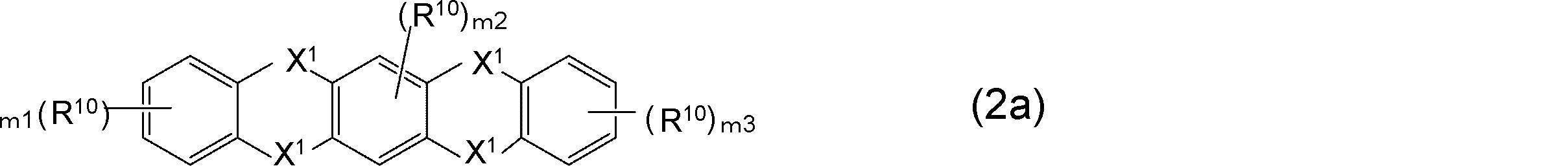
(前記一般式(2a)において、R10は、前記一般式(2)におけるR1~R8と同義である。
m1およびm3は0から4までの整数、m2は0から2までの整数を表す。
複数のR10は、互いに同じまたは異なる。
X1は前記式(41)~(45)から選ばれる連結基のいずれかを表す。
複数のX1は、互いに同じ、または異なる。
ただし、前記一般式(2a)において、R10および前記式(43)~(45)のRxのうち一つは、Lに対して結合する単結合である。)
m1およびm3は0から4までの整数、m2は0から2までの整数を表す。
複数のR10は、互いに同じまたは異なる。
X1は前記式(41)~(45)から選ばれる連結基のいずれかを表す。
複数のX1は、互いに同じ、または異なる。
ただし、前記一般式(2a)において、R10および前記式(43)~(45)のRxのうち一つは、Lに対して結合する単結合である。)
本発明の有機エレクトロルミネッセンス素子において、
前記一般式(5)におけるR31~R38の少なくともいずれか1つは、下記一般式(51)で表されることが好ましい。
前記一般式(5)におけるR31~R38の少なくともいずれか1つは、下記一般式(51)で表されることが好ましい。

(前記一般式(51)において、
R39は、前記一般式(2)におけるR1~R8と同義である。
rは0から3までの整数を表し、Sは0から4までの整数を表す。
複数のR39は、互いに同一または異なる。
X1は前記一般式(41)~(45)から選ばれる連結基のいずれかを表す。
L61は単結合または連結基である。
連結基は、
置換もしくは無置換の環形成炭素数6~30のアリール基、
置換もしくは無置換の環形成原子数5~30の複素環基、または
これらの基が互いに2~5個連結した基のいずれかから誘導される基である。
なお、互いに連結した基は、互いに同一または異なる。)
R39は、前記一般式(2)におけるR1~R8と同義である。
rは0から3までの整数を表し、Sは0から4までの整数を表す。
複数のR39は、互いに同一または異なる。
X1は前記一般式(41)~(45)から選ばれる連結基のいずれかを表す。
L61は単結合または連結基である。
連結基は、
置換もしくは無置換の環形成炭素数6~30のアリール基、
置換もしくは無置換の環形成原子数5~30の複素環基、または
これらの基が互いに2~5個連結した基のいずれかから誘導される基である。
なお、互いに連結した基は、互いに同一または異なる。)
本発明の有機エレクトロルミネッセンス素子において、
前記一般式(1)におけるAが、下記一般式(8),(9),(10),(11),(12),(13)および(14)のいずれかで表されることが好ましい。
前記一般式(1)におけるAが、下記一般式(8),(9),(10),(11),(12),(13)および(14)のいずれかで表されることが好ましい。
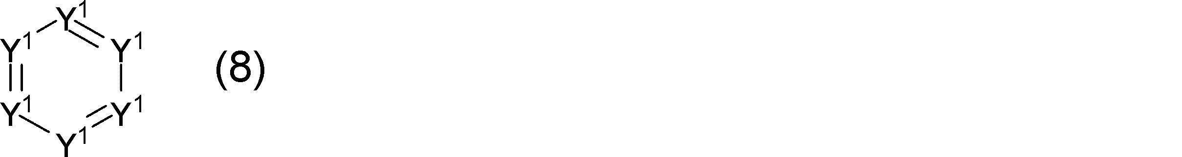
(前記一般式(8)において、Y1のうち2~4個は窒素原子であり、1つは、Lに結合する炭素原子であり、その他のY1は、CRyである。
前記一般式(8)が複数のRyを有する場合、Ryは、それぞれ独立して、
水素原子、
フッ素原子、
シアノ基、
ニトロ基、
置換もしくは無置換の環形成炭素数6~30のアリール基、
置換もしくは無置換の環形成原子数5~30の複素環基、
置換もしくは無置換の炭素数1~30のアルキル基、
置換もしくは無置換の炭素数1~30のアルキルカルボニル基、
置換もしくは無置換の環形成炭素数6~30のアリールカルボニル基、
置換もしくは無置換の炭素数1~30のアルキルスルフィニル基、
置換もしくは無置換の環形成炭素数6~30のアリールスルフィニル基、
置換もしくは無置換の炭素数2~60のアルキルホスフィニル基、
置換もしくは無置換の環形成炭素数6~60のアリールホスフィニル基、
置換もしくは無置換の炭素数1~30のアルキルスルホニル基、
置換もしくは無置換の環形成炭素数6~30のアリールスルホニル基、
置換もしくは無置換の炭素数3~60のアルキルシリル基、
置換もしくは無置換の環形成炭素数8~60のアリールシリル基、
置換もしくは無置換の炭素数1~30のアルコキシ基、または、
置換もしくは無置換の環形成炭素数6~30のアリールオキシ基である。
隣接する2つのY1がCRyであるとき、隣接する2つのY1が飽和または不飽和の環構造を形成していてもよい。)

(前記一般式(9)において、Y2は前記一般式(8)におけるY1と同義である。)

(前記一般式(10),(11),(12)において、
Y3は前記一般式(8)におけるY1と同義である。
X3は下記一般式(41)~(45)から選ばれる連結基のいずれかを表す。)
Y3は前記一般式(8)におけるY1と同義である。
X3は下記一般式(41)~(45)から選ばれる連結基のいずれかを表す。)
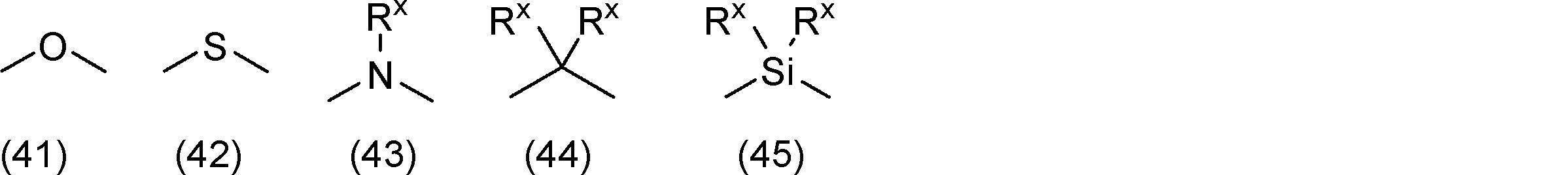
(前記一般式(43)~(45)において、
Rxは、それぞれ独立に、
水素原子、
置換もしくは無置換の炭素数6~30のアリール基、
置換もしくは無置換の環形成原子数5~30の複素環基、または
置換もしくは無置換の炭素数1~30のアルキル基である。
複数のRxが存在する場合は互いに同じまたは異なる。)
Rxは、それぞれ独立に、
水素原子、
置換もしくは無置換の炭素数6~30のアリール基、
置換もしくは無置換の環形成原子数5~30の複素環基、または
置換もしくは無置換の炭素数1~30のアルキル基である。
複数のRxが存在する場合は互いに同じまたは異なる。)

(前記一般式(13)において、
R41~R48のうち一つはLに対して結合する単結合であり、
その他のR41~R48は、前記一般式(8)におけるRyと同義である。
L4は下記一般式(131)~(136)から選ばれる連結基のいずれかを表す。
pは1~3の整数を表し、pが2または3の場合、複数のL4は互いに同じまたは異なる。)
R41~R48のうち一つはLに対して結合する単結合であり、
その他のR41~R48は、前記一般式(8)におけるRyと同義である。
L4は下記一般式(131)~(136)から選ばれる連結基のいずれかを表す。
pは1~3の整数を表し、pが2または3の場合、複数のL4は互いに同じまたは異なる。)

(前記一般式(133)~(136)において、
R301は、それぞれ独立に、
水素原子、
置換もしくは無置換の環形成炭素数6~30のアリール基、
置換もしくは無置換の環形成原子数5~30の複素環基、または
置換もしくは無置換の炭素数1~30のアルキル基である。
複数のR301が存在する場合は互いに同じまたは異なる。)
R301は、それぞれ独立に、
水素原子、
置換もしくは無置換の環形成炭素数6~30のアリール基、
置換もしくは無置換の環形成原子数5~30の複素環基、または
置換もしくは無置換の炭素数1~30のアルキル基である。
複数のR301が存在する場合は互いに同じまたは異なる。)
(前記一般式(14)において、
Araは、
置換もしくは無置換の環形成炭素数6~30のアリール基、または、
置換もしくは無置換の環形成原子数5~30の複素環基である。
Zaは、
フッ素原子、
シアノ基、
ニトロ基、
置換もしくは無置換の炭素数1~20のアルキルカルボニル基、
置換もしくは無置換の環形成炭素数6~30のアリールカルボニル基、
置換もしくは無置換の炭素数1~20のアルキルスルフィニル基、
置換もしくは無置換の環形成炭素数6~30のアリールスルフィニル基、
置換もしくは無置換の炭素数2~60のアルキルホスフィニル基、
置換もしくは無置換の環形成炭素数6~60のアリールホスフィニル基、
置換もしくは無置換の炭素数1~30のアルキルスルホニル基、または、
置換もしくは無置換の環形成炭素数6~30のアリールスルホニル基である。
qは、Araに直接結合するZaの置換数を表す1~5の整数であり、
qが2以上の場合、複数のZaは、互いに同一または異なる。)
前記一般式(1)で表される第1の材料としては、下記一般式(101)で表されるビスカルバゾール誘導体が好ましい。
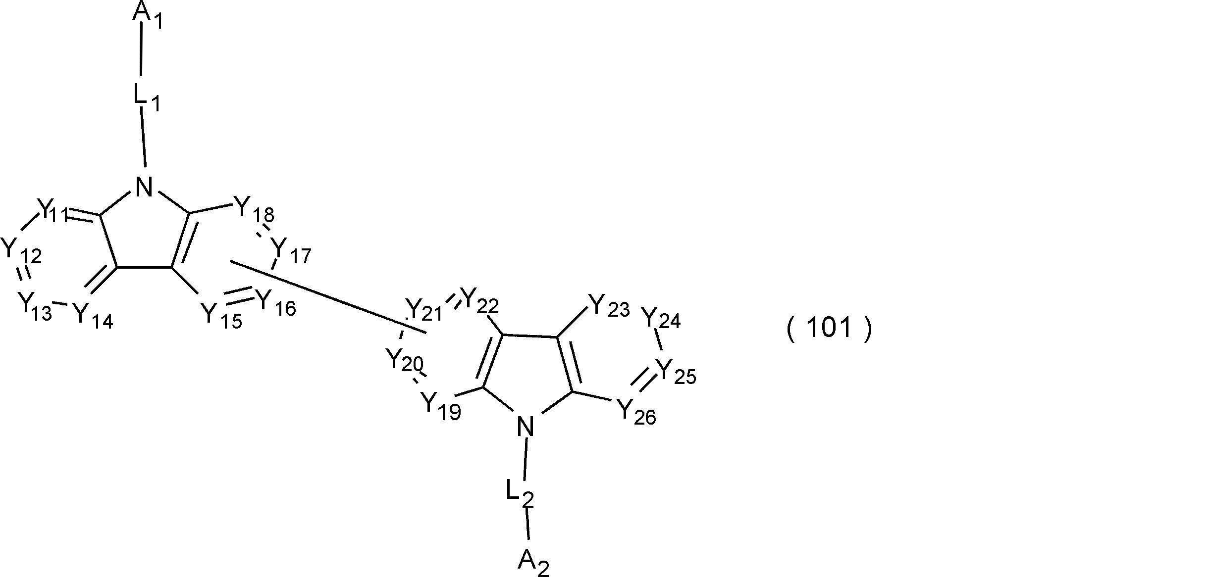
上記一般式(101)において、A1及びA2は、互いに独立して、
水素原子、
ハロゲン原子、
シアノ基、
置換もしくは無置換の環形成炭素数6~30のアリール基、
置換もしくは無置換の環形成原子数5~30の複素環基、
置換もしくは無置換の炭素数1~30のアルキル基、
置換もしくは無置換の炭素数1~30のアルコキシ基、
置換もしくは無置換の炭素数7~30のアラルキル基、
置換もしくは無置換の環形成炭素数6~30のアリールオキシ基、
置換もしくは無置換の炭素数3~60のアルキルシリル基、または
置換もしくは無置換の環形成炭素数8~30のアリールシリル基を表す。
但し、A1及びA2の少なくとも1つは、シアノ基であることが好ましい。
水素原子、
ハロゲン原子、
シアノ基、
置換もしくは無置換の環形成炭素数6~30のアリール基、
置換もしくは無置換の環形成原子数5~30の複素環基、
置換もしくは無置換の炭素数1~30のアルキル基、
置換もしくは無置換の炭素数1~30のアルコキシ基、
置換もしくは無置換の炭素数7~30のアラルキル基、
置換もしくは無置換の環形成炭素数6~30のアリールオキシ基、
置換もしくは無置換の炭素数3~60のアルキルシリル基、または
置換もしくは無置換の環形成炭素数8~30のアリールシリル基を表す。
但し、A1及びA2の少なくとも1つは、シアノ基であることが好ましい。
上記一般式(101)において、Y11~Y14およびY23~Y26は、互いに独立して、C(R)または窒素原子を表し、Y15~Y18は、互いに独立して、C(R)、窒素原子またはY19~Y22のいずれかと結合する炭素原子を表し、Y19~Y22は、互いに独立して、C(R)、窒素原子またはY15~Y18のいずれかと結合する炭素原子を表し、Rは、それぞれ独立に、水素原子または置換基を表す。Rにおける置換基は、上述のA1およびA2が置換基を有する場合の置換基と同義である。
上記一般式(101)において、L1及びL2は、互いに独立して、
単結合、
置換もしくは無置換の環形成炭素数6~30の2価の芳香族炭化水素基、
置換もしくは無置換の環形成原子数5~30の2価の複素環基、または
当該2価の芳香族炭化水素基および当該2価の複素環基が連結した基を表す。
単結合、
置換もしくは無置換の環形成炭素数6~30の2価の芳香族炭化水素基、
置換もしくは無置換の環形成原子数5~30の2価の複素環基、または
当該2価の芳香族炭化水素基および当該2価の複素環基が連結した基を表す。
また、前記L1及び前記L2の少なくとも一方が、下記一般式(a)で表されることが好ましい。

上記一般式(a)において、Y31~Y35は、互いに独立して、C(Ra)、窒素原子またはL3と結合する炭素原子を表し、Raは、それぞれ独立に、水素原子又は置換基を表す。Raにおける置換基は、上述のA1およびA2が置換基を有する場合の置換基と同義である。
上記一般式(a)において、L3及びL4は、互いに独立して
単結合、
置換もしくは無置換の環形成炭素数6~30の2価の芳香族炭化水素基、
置換もしくは無置換の環形成原子数5~30の2価の複素環基、または
当該2価の芳香族炭化水素基および当該2価の複素環基が連結した基を表す。
上記一般式(a)において、L3及びL4は、互いに独立して
単結合、
置換もしくは無置換の環形成炭素数6~30の2価の芳香族炭化水素基、
置換もしくは無置換の環形成原子数5~30の2価の複素環基、または
当該2価の芳香族炭化水素基および当該2価の複素環基が連結した基を表す。
本発明の有機エレクトロルミネッセンス素子において、
前記蛍光発光性ドーパント材料である第二の材料は、下記一般式(20)で表されることが好ましい。
前記蛍光発光性ドーパント材料である第二の材料は、下記一般式(20)で表されることが好ましい。

(前記一般式(20)において、
Ar0は、置換もしくは無置換の環形成炭素数10~50の2価の縮合芳香族炭化水素基であり、
Ar1~Ar4は、それぞれ独立に、
置換もしくは無置換の環形成炭素数6~30のアリール基、
置換もしくは無置換の環形成原子数5~30の複素環基、
置換もしくは無置換の炭素数6~30のアルキル基、または、
置換もしくは無置換の炭素数7~30のアラルキル基である。)
Ar0は、置換もしくは無置換の環形成炭素数10~50の2価の縮合芳香族炭化水素基であり、
Ar1~Ar4は、それぞれ独立に、
置換もしくは無置換の環形成炭素数6~30のアリール基、
置換もしくは無置換の環形成原子数5~30の複素環基、
置換もしくは無置換の炭素数6~30のアルキル基、または、
置換もしくは無置換の炭素数7~30のアラルキル基である。)
本発明の有機エレクトロルミネッセンス素子において、
遅延蛍光比率が37.5%より大きい
ことが好ましい。
遅延蛍光比率が37.5%より大きい
ことが好ましい。
本発明の有機エレクトロルミネッセンス素子において、
過渡EL測定における電圧除去後1μs経過後の残存強度比が36.0%より大きい
ことが好ましい。
過渡EL測定における電圧除去後1μs経過後の残存強度比が36.0%より大きい
ことが好ましい。
本発明の有機エレクトロルミネッセンス素子において、
前記第一の材料のフォトルミネッセンススペクトルの半値幅が50nm以上である
ことが好ましい。
前記第一の材料のフォトルミネッセンススペクトルの半値幅が50nm以上である
ことが好ましい。
また、本発明の有機エレクトロルミネッセンス素子として、発光層に含まれる第二の材料が、重金属錯体ではないドーパント材料を用いた形態となる場合もある。
すなわち、この場合の本発明の有機エレクトロルミネッセンス素子は、陰極と、陽極と、前記陰極と前記陽極との間に配置された、少なくとも発光層を含む1層以上の有機薄膜層と、を有し、前記発光層が、前記一般式(1)で表される第一の材料とドーパント材料である第二の材料とを含むことを特徴とする。但し、前記ドーパント材料は、重金属錯体ではない。この場合の一般式(1)で表される第一の材料については、上述と同義である。
すなわち、この場合の本発明の有機エレクトロルミネッセンス素子は、陰極と、陽極と、前記陰極と前記陽極との間に配置された、少なくとも発光層を含む1層以上の有機薄膜層と、を有し、前記発光層が、前記一般式(1)で表される第一の材料とドーパント材料である第二の材料とを含むことを特徴とする。但し、前記ドーパント材料は、重金属錯体ではない。この場合の一般式(1)で表される第一の材料については、上述と同義である。
一方、本発明の有機エレクトロルミネッセンス素子用材料は、下記一般式(1)で表される第一の材料と蛍光発光性ドーパント材料である第二の材料とを含むことを特徴とする。
(前記一般式(1)において、
Aは下記一般式(a-1)~(a-7)から選ばれる部分構造を有する基であり、
Bは下記一般式(b-1)~(b-6)から選ばれる部分構造を有する基であり、
Lは、単結合または連結基である。
連結基は、
置換もしくは無置換の環形成炭素数6~30のアリール基、
置換もしくは無置換の環形成原子数5~30の複素環基、または
これらの基が互いに2~5個連結した基のいずれかから誘導される基である。
なお、互いに連結した基は、互いに同一または異なる。
aは、Lに直接結合するAの置換数を表す1~5の整数であり、
aが2以上の場合、複数のAは互いに同じまたは異なる。
bは、Lに直接結合するBの置換数を表す1~5の整数であり、
bが2以上の場合、複数のBは互いに同じまたは異なる。)
Aは下記一般式(a-1)~(a-7)から選ばれる部分構造を有する基であり、
Bは下記一般式(b-1)~(b-6)から選ばれる部分構造を有する基であり、
Lは、単結合または連結基である。
連結基は、
置換もしくは無置換の環形成炭素数6~30のアリール基、
置換もしくは無置換の環形成原子数5~30の複素環基、または
これらの基が互いに2~5個連結した基のいずれかから誘導される基である。
なお、互いに連結した基は、互いに同一または異なる。
aは、Lに直接結合するAの置換数を表す1~5の整数であり、
aが2以上の場合、複数のAは互いに同じまたは異なる。
bは、Lに直接結合するBの置換数を表す1~5の整数であり、
bが2以上の場合、複数のBは互いに同じまたは異なる。)


(前記一般式(b-1)~(b-6)において、
Rは、
水素原子、
置換もしくは無置換の環形成炭素数6~30のアリール基、
置換もしくは無置換の環形成原子数5~30の複素環基、または
置換もしくは無置換の炭素数1~30のアルキル基、である。
複数のRが存在する場合は互いに同じまたは異なる。複数のRは互いに結合して環を形成する場合と、しない場合とがある。)
Rは、
水素原子、
置換もしくは無置換の環形成炭素数6~30のアリール基、
置換もしくは無置換の環形成原子数5~30の複素環基、または
置換もしくは無置換の炭素数1~30のアルキル基、である。
複数のRが存在する場合は互いに同じまたは異なる。複数のRは互いに結合して環を形成する場合と、しない場合とがある。)
本発明の有機EL素子は、実用的な高電流密度領域においても効率的に発光する。
(有機EL素子の素子構成)
以下、本発明に係る有機EL素子の素子構成について説明する。
本発明の有機EL素子は、一対の電極間に有機化合物層を備える。この有機化合物層は、有機化合物で構成される層を少なくとも一層、有する。有機化合物層は、無機化合物を含んでいてもよい。
本発明の有機EL素子において、有機化合物層のうち少なくとも1層は、発光層を有する。そのため、有機化合物層は、例えば、一層の発光層で構成されていてもよいし、正孔注入層、正孔輸送層、電子注入層、電子輸送層、正孔障壁層、電子障壁層等の公知の有機EL素子で採用される層を有していてもよい。
以下、本発明に係る有機EL素子の素子構成について説明する。
本発明の有機EL素子は、一対の電極間に有機化合物層を備える。この有機化合物層は、有機化合物で構成される層を少なくとも一層、有する。有機化合物層は、無機化合物を含んでいてもよい。
本発明の有機EL素子において、有機化合物層のうち少なくとも1層は、発光層を有する。そのため、有機化合物層は、例えば、一層の発光層で構成されていてもよいし、正孔注入層、正孔輸送層、電子注入層、電子輸送層、正孔障壁層、電子障壁層等の公知の有機EL素子で採用される層を有していてもよい。
有機EL素子の代表的な素子構成としては、
(a)陽極/発光層/陰極
(b)陽極/正孔注入・輸送層/発光層/陰極
(c)陽極/発光層/電子注入・輸送層/陰極
(d)陽極/正孔注入・輸送層/発光層/電子注入・輸送層/陰極
(e)陽極/正孔注入・輸送層/発光層/障壁層/電子注入・輸送層/陰極
などの構造を挙げることができる。
上記の中で(d)の構成が好ましく用いられるが、もちろんこれらに限定されるものではない。
なお、上記「発光層」とは、一般的にドーピングシステムが採用されており、第一の材料と第二の材料とを含む有機化合物層である。第一の材料は、一般的に電子と正孔の再結合を促し、再結合により生じた励起エネルギーを第二の材料に伝達させる。このような第一の材料は、ホスト材料と呼ばれることが多く、以下の説明でも、第一の材料のことをホスト材料という。また、第二の材料は、一般的にホスト材料(第一の材料)から励起エネルギーを受け取り、高い発光性能を示す。このような第二の材料は、ドーパント材料と呼ばれることが多く、以下の説明でも、第二の材料のことをドーパント材料という。ドーパント材料としては、量子収率の高い化合物が好まれる。本発明では、ドーパント材料は、蛍光発光を示す材料(蛍光発光性ドーパント材料)が用いられる。
上記「正孔注入・輸送層」は「正孔注入層および正孔輸送層のうちの少なくともいずれか1つ」を意味し、「電子注入・輸送層」は「電子注入層および電子輸送層のうちの少なくともいずれか1つ」を意味する。ここで、正孔注入層および正孔輸送層を有する場合には、陽極側に正孔注入層が設けられていることが好ましい。また、電子注入層および電子輸送層を有する場合には、陰極側に電子注入層が設けられていることが好ましい。
本発明において電子輸送層といった場合には、発光層と陰極との間に存在する電子輸送領域の有機層のうち、最も電子移動度の高い有機層をいう。電子輸送領域が一層で構成されている場合には、当該層が電子輸送層である。また、発光層と電子輸送層との間には、構成(e)に示すように発光層で生成された励起エネルギーの拡散を防ぐ目的で、必ずしも電子移動度の高くない障壁層が設けられることがある。そのため、発光層に隣接する有機層が電子輸送層に必ずしも該当しない。
図1に、本発明の実施形態における有機EL素子の一例の概略構成を示す。
有機EL素子1は、透光性の基板2と、陽極3と、陰極4と、陽極3と陰極4との間に配置された有機化合物層10と、を有する。
有機化合物層10は、ホスト材料およびドーパント材料を含む発光層5を有する。また、有機化合物層10は、発光層5と陽極3との間に、陽極3から順に、正孔注入層6、正孔輸送層7を有する。さらに、有機化合物層10は、発光層5と陰極4との間に、発光層5側から順に、電子輸送層8、電子注入層9を有する。
有機EL素子1は、透光性の基板2と、陽極3と、陰極4と、陽極3と陰極4との間に配置された有機化合物層10と、を有する。
有機化合物層10は、ホスト材料およびドーパント材料を含む発光層5を有する。また、有機化合物層10は、発光層5と陽極3との間に、陽極3から順に、正孔注入層6、正孔輸送層7を有する。さらに、有機化合物層10は、発光層5と陰極4との間に、発光層5側から順に、電子輸送層8、電子注入層9を有する。
(発光層)
〔発光層の化合物〕
本発明において、ホスト材料、及びドーパント材料に用いる化合物は、次の通りである。
・ホスト材料
ホスト材料としては、下記一般式(1)で表される第一の材料を用いることができる。
〔発光層の化合物〕
本発明において、ホスト材料、及びドーパント材料に用いる化合物は、次の通りである。
・ホスト材料
ホスト材料としては、下記一般式(1)で表される第一の材料を用いることができる。
(前記一般式(1)において、
Aは下記一般式(a-1)~(a-7)から選ばれる部分構造を有する基であり、
Bは下記一般式(b-1)~(b-6)から選ばれる部分構造を有する基であり、
Lは、単結合または連結基である。
連結基は、
置換もしくは無置換の環形成炭素数6~30のアリール基、
置換もしくは無置換の環形成原子数5~30の複素環基、または
これらの基が互いに2~5個連結した基のいずれかから誘導される基である。
なお、互いに連結した基は、互いに同一または異なる。
aは、Lに直接結合するAの置換数を表す1~5の整数であり、
aが2以上の場合、複数のAは互いに同じまたは異なる。
bは、Lに直接結合するBの置換数を表す1~5の整数であり、
bが2以上の場合、複数のBは互いに同じまたは異なる。)
Aは下記一般式(a-1)~(a-7)から選ばれる部分構造を有する基であり、
Bは下記一般式(b-1)~(b-6)から選ばれる部分構造を有する基であり、
Lは、単結合または連結基である。
連結基は、
置換もしくは無置換の環形成炭素数6~30のアリール基、
置換もしくは無置換の環形成原子数5~30の複素環基、または
これらの基が互いに2~5個連結した基のいずれかから誘導される基である。
なお、互いに連結した基は、互いに同一または異なる。
aは、Lに直接結合するAの置換数を表す1~5の整数であり、
aが2以上の場合、複数のAは互いに同じまたは異なる。
bは、Lに直接結合するBの置換数を表す1~5の整数であり、
bが2以上の場合、複数のBは互いに同じまたは異なる。)
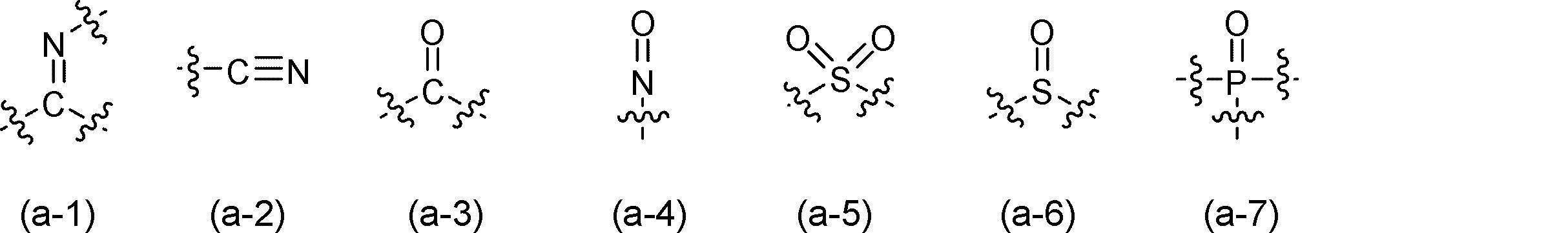

(前記一般式(b-1)~(b-6)において、
Rは、
水素原子、
置換もしくは無置換の環形成炭素数6~30のアリール基、
置換もしくは無置換の環形成原子数5~30の複素環基、または
置換もしくは無置換の炭素数1~30のアルキル基、である。
複数のRが存在する場合は互いに同じまたは異なる。複数のRは互いに結合して環を形成する場合と、しない場合とがある。)
Rは、
水素原子、
置換もしくは無置換の環形成炭素数6~30のアリール基、
置換もしくは無置換の環形成原子数5~30の複素環基、または
置換もしくは無置換の炭素数1~30のアルキル基、である。
複数のRが存在する場合は互いに同じまたは異なる。複数のRは互いに結合して環を形成する場合と、しない場合とがある。)
前記一般式(1)において、Bはドナー要素を有する構造であり、Aはアクセプター要素を有する構造である。すなわち、Bの有する上記一般式(b-1)~(b-6)から選ばれる部分構造がドナー要素を有する構造であり、Aの有する上記一般式(a-1)~(a-7)から選ばれる部分構造がアクセプター要素を有する構造である。なお、ドナー要素とは、電子供与性を指し、アクセプター要素とは、電子受容性を指す。
前記一般式(1)は、下記一般式(1a)~(1g)のいずれかであることが好ましい。
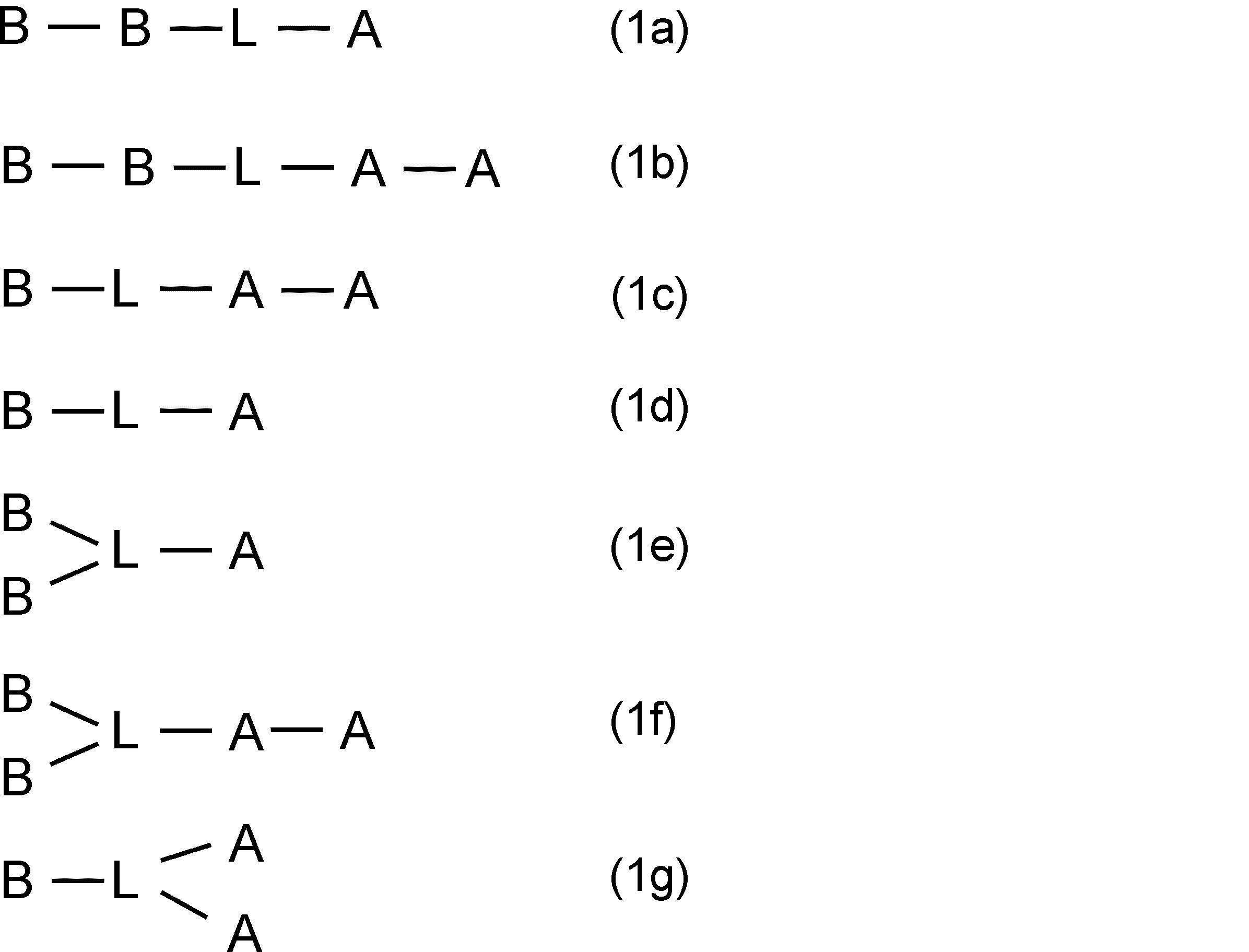
前記一般式(1)および(b-1)~(b-6)において、環形成炭素数6~30のアリール基としては、縮合アリール基も含まれ、例えば、フェニル基、1-ナフチル基、2-ナフチル基、1-アントリル基、2-アントリル基、9-アントリル基、ベンズアントリル基、1-フェナントリル基、2-フェナントリル基、3-フェナントリル基、4-フェナントリル基、9-フェナントリル基、ナフタセニル基、ピレニル基、1-クリセニル基、2-クリセニル基、3-クリセニル基、4-クリセニル基、5-クリセニル基、6-クリセニル基、ベンゾ[c]フェナントリル基、ベンゾ[g]クリセニル基、1-トリフェニレニル基、2-トリフェニレニル基、3-トリフェニレニル基、4-トリフェニレニル基、1-フルオレニル基、2-フルオレニル基、3-フルオレニル基、4-フルオレニル基、9-フルオレニル基、ベンゾフルオレニル基、ジベンゾフルオレニル基、2-ビフェニルイル基、3-ビフェニルイル基、4-ビフェニルイル基、o-ターフェニル基、m-ターフェニル-4-イル基、m-ターフェニル-3-イル基、m-ターフェニル-2-イル基、p-ターフェニル-4-イル基、p-ターフェニル-3-イル基、p-ターフェニル-2-イル基、m-クウォーターフェニル基、3-フルオランテニル基、4-フルオランテニル基、8-フルオランテニル基、9-フルオランテニル基、ベンゾフルオランテニル基、o-トリル基、m-トリル基、p-トリル基、2,3-キシリル基、3,4-キシリル基、2,5-キシリル基、メシチル基、o-クメニル基、m-クメニル基、p-クメニル基、p-t-ブチルフェニル基、p-(2-フェニルプロピル)フェニル基、4’-メチルビフェニルイル基、4”-t-ブチル-p-ターフェニル-4-イル基が挙げられる。
アリール基としては、環形成炭素数が6~20であることが好ましく、より好ましくは6~12であることが好ましい。上記アリール基の中でもフェニル基、ビフェニル基、ナフチル基、フェナントリル基、ターフェニル基が特に好ましい。
アリール基としては、環形成炭素数が6~20であることが好ましく、より好ましくは6~12であることが好ましい。上記アリール基の中でもフェニル基、ビフェニル基、ナフチル基、フェナントリル基、ターフェニル基が特に好ましい。
環形成原子数5~30の複素環基としては、縮合複素環基も含まれ、例えば、ピロリル基、ピラジニル基、ピリジニル基、インドリル基、イソインドリル基、イミダゾリル基、フリル基、ベンゾフラニル基、イソベンゾフラニル基、ジベンゾフラニル基、ジベンゾチオフェニル基、キノリル基、イソキノリル基、キノキサリニル基、カルバゾリル基、フェナントリジニル基、アクリジニル基、フェナントロリニル基、フェナジニル基、フェノチアジニル基、フェノキサジニル基、オキサゾリル基、オキサジアゾリル基、フラザニル基、チエニル基、ベンゾチオフェニル基、ピリジン環、ピラジン環、ピリミジン環、ピリダジン環、トリアジン環、インドール環、キノリン環、アクリジン環、ピロリジン環、ジオキサン環、ピペリジン環、モルフォリン環、ピペラジン環、カルバゾール環、フラン環、チオフェン環、オキサゾール環、オキサジアゾール環、ベンゾオキサゾール環、チアゾール環、チアジアゾール環、ベンゾチアゾール環、トリアゾール環、イミダゾール環、ベンゾイミダゾール環、ピラン環、ジベンゾフラン環から形成される基が挙げられる。
さらに具体的には、1-ピロリル基、2-ピロリル基、3-ピロリル基、ピラジニル基、2-ピリジニル基、2-ピリミジニル基、4-ピリミジニル基、5-ピリミジニル基、6-ピリミジニル基、1,2,3-トリアジン-4-イル基、1,2,4-トリアジン-3-イル基、1,3,5-トリアジン-2-イル基、1-イミダゾリル基、2-イミダゾリル基、1-ピラゾリル基、1-インドリジニル基、2-インドリジニル基、3-インドリジニル基、5-インドリジニル基、6-インドリジニル基、7-インドリジニル基、8-インドリジニル基、2-イミダゾピリジニル基、3-イミダゾピリジニル基、5-イミダゾピリジニル基、6-イミダゾピリジニル基、7-イミダゾピリジニル基、8-イミダゾピリジニル基、3-ピリジニル基、4-ピリジニル基、1-インドリル基、2-インドリル基、3-インドリル基、4-インドリル基、5-インドリル基、6-インドリル基、7-インドリル基、1-イソインドリル基、2-イソインドリル基、3-イソインドリル基、4-イソインドリル基、5-イソインドリル基、6-イソインドリル基、7-イソインドリル基、2-フリル基、3-フリル基、2-ベンゾフラニル基、3-ベンゾフラニル基、4-ベンゾフラニル基、5-ベンゾフラニル基、6-ベンゾフラニル基、7-ベンゾフラニル基、1-イソベンゾフラニル基、3-イソベンゾフラニル基、4-イソベンゾフラニル基、5-イソベンゾフラニル基、6-イソベンゾフラニル基、7-イソベンゾフラニル基、2-キノリル基、3-キノリル基、4-キノリル基、5-キノリル基、6-キノリル基、7-キノリル基、8-キノリル基、1-イソキノリル基、3-イソキノリル基、4-イソキノリル基、5-イソキノリル基、6-イソキノリル基、7-イソキノリル基、8-イソキノリル基、2-キノキサリニル基、5-キノキサリニル基、6-キノキサリニル基、1-カルバゾリル基、2-カルバゾリル基、3-カルバゾリル基、4-カルバゾリル基、9-カルバゾリル基、アザカルバゾリル-1-イル基、アザカルバゾリル-2-イル基、アザカルバゾリル-3-イル基、アザカルバゾリル-4-イル基、アザカルバゾリル-5-イル基、アザカルバゾリル-6-イル基、アザカルバゾリル-7-イル基、アザカルバゾリル-8-イル基、アザカルバゾリル-9-イル基、1-フェナントリジニル基、2-フェナントリジニル基、3-フェナントリジニル基、4-フェナントリジニル基、6-フェナントリジニル基、7-フェナントリジニル基、8-フェナントリジニル基、9-フェナントリジニル基、10-フェナントリジニル基、1-アクリジニル基、2-アクリジニル基、3-アクリジニル基、4-アクリジニル基、9-アクリジニル基、1,7-フェナントロリン-2-イル基、1,7-フェナントロリン-3-イル基、1,7-フェナントロリン-4-イル基、1,7-フェナントロリン-5-イル基、1,7-フェナントロリン-6-イル基、1,7-フェナントロリン-8-イル基、1,7-フェナントロリン-9-イル基、1,7-フェナントロリン-10-イル基、1,8-フェナントロリン-2-イル基、1,8-フェナントロリン-3-イル基、1,8-フェナントロリン-4-イル基、1,8-フェナントロリン-5-イル基、1,8-フェナントロリン-6-イル基、1,8-フェナントロリン-7-イル基、1,8-フェナントロリン-9-イル基、1,8-フェナントロリン-10-イル基、1,9-フェナントロリン-2-イル基、1,9-フェナントロリン-3-イル基、1,9-フェナントロリン-4-イル基、1,9-フェナントロリン-5-イル基、1,9-フェナントロリン-6-イル基、1,9-フェナントロリン-7-イル基、1,9-フェナントロリン-8-イル基、1,9-フェナントロリン-10-イル基、1,10-フェナントロリン-2-イル基、1,10-フェナントロリン-3-イル基、1,10-フェナントロリン-4-イル基、1,10-フェナントロリン-5-イル基、2,9-フェナントロリン-1-イル基、2,9-フェナントロリン-3-イル基、2,9-フェナントロリン-4-イル基、2,9-フェナントロリン-5-イル基、2,9-フェナントロリン-6-イル基、2,9-フェナントロリン-7-イル基、2,9-フェナントロリン-8-イル基、2,9-フェナントロリン-10-イル基、2,8-フェナントロリン-1-イル基、2,8-フェナントロリン-3-イル基、2,8-フェナントロリン-4-イル基、2,8-フェナントロリン-5-イル基、2,8-フェナントロリン-6-イル基、2,8-フェナントロリン-7-イル基、2,8-フェナントロリン-9-イル基、2,8-フェナントロリン-10-イル基、2,7-フェナントロリン-1-イル基、2,7-フェナントロリン-3-イル基、2,7-フェナントロリン-4-イル基、2,7-フェナントロリン-5-イル基、2,7-フェナントロリン-6-イル基、2,7-フェナントロリン-8-イル基、2,7-フェナントロリン-9-イル基、2,7-フェナントロリン-10-イル基、1-フェナジニル基、2-フェナジニル基、1-フェノチアジニル基、2-フェノチアジニル基、3-フェノチアジニル基、4-フェノチアジニル基、10-フェノチアジニル基、1-フェノキサジニル基、2-フェノキサジニル基、3-フェノキサジニル基、4-フェノキサジニル基、10-フェノキサジニル基、2-オキサゾリル基、4-オキサゾリル基、5-オキサゾリル基、2-オキサジアゾリル基、5-オキサジアゾリル基、3-フラザニル基、2-チエニル基、3-チエニル基、2-メチルピロール-1-イル基、2-メチルピロール-3-イル基、2-メチルピロール-4-イル基、2-メチルピロール-5-イル基、3-メチルピロール-1-イル基、3-メチルピロール-2-イル基、3-メチルピロール-4-イル基、3-メチルピロール-5-イル基、2-t-ブチルピロール-4-イル基、3-(2-フェニルプロピル)ピロール-1-イル基、2-メチル-1-インドリル基、4-メチル-1-インドリル基、2-メチル-3-インドリル基、4-メチル-3-インドリル基、2-t-ブチル-1-インドリル基、4-t-ブチル-1-インドリル基、2-t-ブチル-3-インドリル基、4-t-ブチル-3-インドリル基、1-ジベンゾフラニル基、2-ジベンゾフラニル基、3-ジベンゾフラニル基、4-ジベンゾフラニル基、1-ジベンゾチオフェニル基、2-ジベンゾチオフェニル基、3-ジベンゾチオフェニル基、4-ジベンゾチオフェニル基、1-シラフルオレニル基、2-シラフルオレニル基、3-シラフルオレニル基、4-シラフルオレニル基、1-ゲルマフルオレニル基、2-ゲルマフルオレニル基、3-ゲルマフルオレニル基、4-ゲルマフルオレニル基が挙げられる。
複素環基の環形成原子数は、5~20であることが好ましく、5~14であることがさらに好ましい。上記複素環基の中でも1-ジベンゾフラニル基、2-ジベンゾフラニル基、3-ジベンゾフラニル基、4-ジベンゾフラニル基、1-ジベンゾチオフェニル基、2-ジベンゾチオフェニル基、3-ジベンゾチオフェニル基、4-ジベンゾチオフェニル基、1-カルバゾリル基、2-カルバゾリル基、3-カルバゾリル基、4-カルバゾリル基、9-カルバゾリル基が好ましい。1-カルバゾリル基、2-カルバゾリル基、3-カルバゾリル基および4-カルバゾリル基については、9位の窒素原子に、置換もしくは無置換の環形成炭素数6~30のアリール基または置換もしくは無置換の環形成原子数5~30の複素環基が置換されていることが好ましい。
前記一般式(b-1)~(b-6)において、炭素数1~30のアルキル基としては、直鎖、分岐鎖又は環状のいずれであってもよい。直鎖または分岐鎖のアルキル基としては、例えば、メチル基、エチル基、プロピル基、イソプロピル基、n-ブチル基、s-ブチル基、イソブチル基、t-ブチル基、n-ペンチル基、n-ヘキシル基、n-ヘプチル基、n-オクチル基、n-ノニル基、n-デシル基、n-ウンデシル基、n-ドデシル基、n-トリデシル基、n-テトラデシル基、n-ペンタデシル基、n-ヘキサデシル基、n-ヘプタデシル基、n-オクタデシル基、ネオペンチル基、1-メチルペンチル基、2-メチルペンチル基、1-ペンチルヘキシル基、1-ブチルペンチル基、1-ヘプチルオクチル基、3-メチルペンチル基、ヒドロキシメチル基、1-ヒドロキシエチル基、2-ヒドロキシエチル基、2-ヒドロキシイソブチル基、1,2-ジヒドロキシエチル基、1,3-ジヒドロキシイソプロピル基、2,3-ジヒドロキシ-t-ブチル基、1,2,3-トリヒドロキシプロピル基、クロロメチル基、1-クロロエチル基、2-クロロエチル基、2-クロロイソブチル基、1,2-ジクロロエチル基、1,3-ジクロロイソプロピル基、2,3-ジクロロ-t-ブチル基、1,2,3-トリクロロプロピル基、ブロモメチル基、1-ブロモエチル基、2-ブロモエチル基、2-ブロモイソブチル基、1,2-ジブロモエチル基、1,3-ジブロモイソプロピル基、2,3-ジブロモ-t-ブチル基、1,2,3-トリブロモプロピル基、ヨードメチル基、1-ヨードエチル基、2-ヨードエチル基、2-ヨードイソブチル基、1,2-ジヨードエチル基、1,3-ジヨードイソプロピル基、2,3-ジヨード-t-ブチル基、1,2,3-トリヨードプロピル基、アミノメチル基、1-アミノエチル基、2-アミノエチル基、2-アミノイソブチル基、1,2-ジアミノエチル基、1,3-ジアミノイソプロピル基、2,3-ジアミノ-t-ブチル基、1,2,3-トリアミノプロピル基、シアノメチル基、1-シアノエチル基、2-シアノエチル基、2-シアノイソブチル基、1,2-ジシアノエチル基、1,3-ジシアノイソプロピル基、2,3-ジシアノ-t-ブチル基、1,2,3-トリシアノプロピル基、ニトロメチル基、1-ニトロエチル基、2-ニトロエチル基、1,2-ジニトロエチル基、2,3-ジニトロ-t-ブチル基、1,2,3-トリニトロプロピル基が挙げられる。
環状のアルキル基(シクロアルキル基)としては、例えば、シクロプロピル基、シクロブチル基、シクロペンチル基、シクロヘキシル基、4-メチルシクロヘキシル基、3,5-テトラメチルシクロヘキシル基、シクロヘプチル基、シクロオクチル基、1-アダマンチル基、2-アダマンチル基、1-ノルボルニル基、2-ノルボルニル基等が挙げられる。
直鎖または分岐鎖のアルキル基の炭素数は、1~10であることが好ましく、1~6であることがさらに好ましい。上記直鎖または分岐鎖のアルキル基の中でもメチル基、エチル基、プロピル基、イソプロピル基、n-ブチル基、s-ブチル基、イソブチル基、t-ブチル基、n-ペンチル基、n-ヘキシル基が好ましい。
シクロアルキル基の環形成炭素数は、3~10であることが好ましく、5~8であることがさらに好ましい。上記シクロアルキル基の中でも、シクロペンチル基やシクロヘキシル基が好ましい。
アルキル基がハロゲン原子で置換されたハロゲン化アルキル基としては、例えば、上記炭素数1~30のアルキル基が1以上のハロゲン基で置換されたものが挙げられる。具体的には、フルオロメチル基、ジフルオロメチル基、トリフルオロメチル基、フルオロエチル基、トリフルオロメチルメチル基等が挙げられる。
前記一般式(1)において、Lとしては、単結合またはフェニル基、ビフェニル基、ターフェニル基、トリフェニレニル基から誘導される2価の基が好ましい。このようなLとすることで、化合物において、LUMO、及びHOMOの電子軌道を重ねないように局在化させることが可能となる。
さらに、前記一般式(1)で表される化合物において、LUMO、及びHOMOの電子軌道を重ねないように局在化させる観点から、前記一般式(1)において、AおよびBが部分構造として縮合芳香族炭化水素を有さないことが好ましい。
前記一般式(b-1)~(b-6)において、Rが置換もしくは無置換の環形成炭素数6~30のアリール基から誘導される基である場合、フェニル基、ビフェニル基、ターフェニル基、トリフェニレニル基が好ましい。
前記一般式(b-1)~(b-6)において、Rが置換もしくは無置換の環形成炭素数6~30のアリール基から誘導される基である場合、フェニル基、ビフェニル基、ターフェニル基、トリフェニレニル基が好ましい。
本発明の有機エレクトロルミネッセンス素子において、前記一般式(1)におけるBが下記一般式(2),(3),(4),(5),および(6)のいずれかで表されることが好ましい。

(前記一般式(2)において、
R1~R8は、それぞれ独立して、
水素原子、
置換もしくは無置換の環形成炭素数6~30のアリール基、
置換もしくは無置換の環形成原子数5~30の複素環基、
置換もしくは無置換の炭素数1~30のアルキル基、
置換もしくは無置換の炭素数3~30のアルキルシリル基、
置換もしくは無置換の環形成炭素数6~60のアリールシリル基、
置換もしくは無置換の炭素数1~30のアルコキシ基、
置換もしくは無置換の環形成炭素数6~30のアリールオキシ基、
置換もしくは無置換の炭素数2~30のアルキルアミノ基、
置換もしくは無置換の環形成炭素数6~60のアリールアミノ基、
置換もしくは無置換の炭素数1~30のアルキルチオ基、または
置換もしくは無置換の環形成炭素数6~30のアリールチオ基である。
ただし、R1とR2、R2とR3、R3とR4、R5とR6、R6とR7、およびR7とR8のいずれかの組み合わせが飽和または不飽和の環構造を形成していてもよい。
L1は、下記一般式(21)~(27)から選ばれる連結基のいずれかを表す。
n1は1~3の整数を表し、n1が2または3の場合、複数のL1は互いに同じまたは異なる。
X1は、下記一般式(41)~(45)から選ばれる連結基のいずれかを表す。)

(前記一般式(23)~(27)において、R101は、前記一般式(2)におけるR1~R8と同義である。
ただし、一般式(2)において、R1~R8のうち一つまたはR101のうち一つは、Lに対して結合する単結合である。
複数のR101が存在する場合は、互いに同じまたは異なる。)
ただし、一般式(2)において、R1~R8のうち一つまたはR101のうち一つは、Lに対して結合する単結合である。
複数のR101が存在する場合は、互いに同じまたは異なる。)

(上記一般式(43)~(45)において、Rxは、
水素原子、
置換もしくは無置換の環形成炭素数6~30のアリール基、
置換もしくは無置換の環形成原子数5~30の複素環基、または
置換もしくは無置換の炭素数1~30のアルキル基である。
複数のRxが存在する場合は互いに同じまたは異なる。)
水素原子、
置換もしくは無置換の環形成炭素数6~30のアリール基、
置換もしくは無置換の環形成原子数5~30の複素環基、または
置換もしくは無置換の炭素数1~30のアルキル基である。
複数のRxが存在する場合は互いに同じまたは異なる。)
上記一般式(2)で表される化合物は、下記一般式(2a)~(2c)のいずれかで表されてもよい。

(前記一般式(2a)において、R10は、前記一般式(2)におけるR1~R8と同義である。
m1およびm3は0から4までの整数、m2は0から2までの整数を表す。
複数のR10は、互いに同じまたは異なる。
X1は上記式(41)~(45)から選ばれる連結基のいずれかを表す。
複数のX1は、互いに同じ、または異なる。
ただし、一般式(2a)において、R10および上記式(43)~(45)のRxのうち一つは、Lに対して結合する単結合である。)
m1およびm3は0から4までの整数、m2は0から2までの整数を表す。
複数のR10は、互いに同じまたは異なる。
X1は上記式(41)~(45)から選ばれる連結基のいずれかを表す。
複数のX1は、互いに同じ、または異なる。
ただし、一般式(2a)において、R10および上記式(43)~(45)のRxのうち一つは、Lに対して結合する単結合である。)
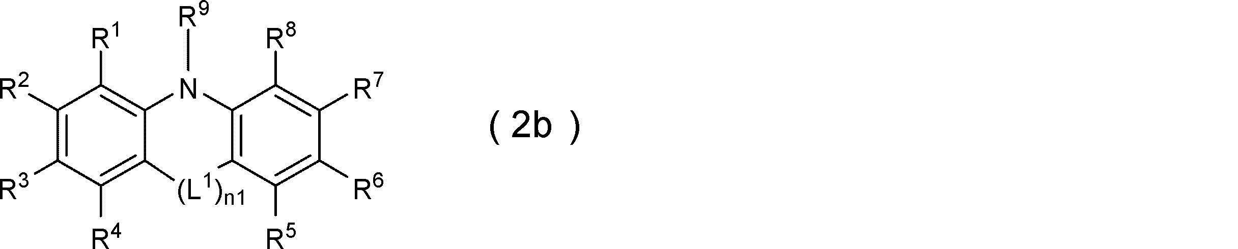
(前記一般式(2b)において、R1~R8、L1、およびn1は上記一般式(2)におけるR1~R8、L1、およびn1と同義である。前記一般式(2b)において、R9は、上記一般式(2)におけるR1~R8と同義である。)
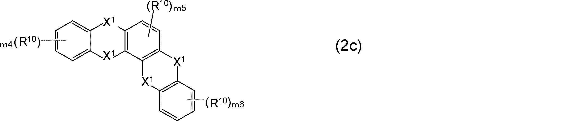
(前記一般式(2c)において、R10は、前記一般式(2)におけるR1~R8と同義である。
m4およびm6は0から4までの整数、m5は0から2までの整数を表す。
複数のR10は、互いに同じまたは異なる。
X1は上記一般式(41)~(45)から選ばれる連結基のいずれかを表す。
複数のX1は、互いに同じ、または異なる。)
m4およびm6は0から4までの整数、m5は0から2までの整数を表す。
複数のR10は、互いに同じまたは異なる。
X1は上記一般式(41)~(45)から選ばれる連結基のいずれかを表す。
複数のX1は、互いに同じ、または異なる。)

(前記一般式(3)において、
R21~R24は、前記一般式(2)におけるR1~R8と同義である。
ただし、R21とR22、R22とR23、およびR23とR24のいずれかの組み合わせが飽和または不飽和の環構造を形成していてもよい。
X1は上記式(41)~(45)から選ばれる連結基のいずれかを表す。)
ただし、前記一般式(3)において、R21~R24およびRxのうち一つは、Lに対して結合する単結合である。)
R21~R24は、前記一般式(2)におけるR1~R8と同義である。
ただし、R21とR22、R22とR23、およびR23とR24のいずれかの組み合わせが飽和または不飽和の環構造を形成していてもよい。
X1は上記式(41)~(45)から選ばれる連結基のいずれかを表す。)
ただし、前記一般式(3)において、R21~R24およびRxのうち一つは、Lに対して結合する単結合である。)

(前記一般式(4)において、
R25~R30は、前記一般式(2)におけるR1~R8と同義である。
ただし、R25とR26、R27とR28、R28とR29、およびR29とR30のいずれかの組み合わせが飽和または不飽和の環構造を形成していてもよい。
X1は上記式(41)~(45)から選ばれる連結基のいずれかを表す。
ただし、前記一般式(4)において、R25~R30およびRxのうちの一つは、Lに対して結合する単結合である。)
R25~R30は、前記一般式(2)におけるR1~R8と同義である。
ただし、R25とR26、R27とR28、R28とR29、およびR29とR30のいずれかの組み合わせが飽和または不飽和の環構造を形成していてもよい。
X1は上記式(41)~(45)から選ばれる連結基のいずれかを表す。
ただし、前記一般式(4)において、R25~R30およびRxのうちの一つは、Lに対して結合する単結合である。)
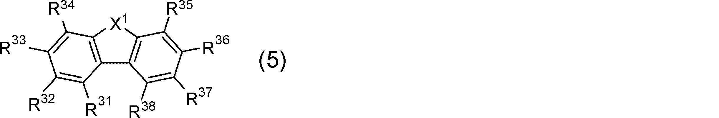
(前記一般式(5)において、
R31~R38は、前記一般式(2)におけるR1~R8と同義である。
ただし、R31とR32、R32とR33、R33とR34、R35とR36、R36とR37、R37とR38のいずれかの組み合わせが飽和または不飽和の環構造を形成していてもよい。
X1は上記一般式(41)~(45)から選ばれる連結基のいずれかを表す。
ただし、前記一般式(5)において、R31~R38およびRxのうちの一つは、Lに対して結合する単結合である。)
R31~R38は、前記一般式(2)におけるR1~R8と同義である。
ただし、R31とR32、R32とR33、R33とR34、R35とR36、R36とR37、R37とR38のいずれかの組み合わせが飽和または不飽和の環構造を形成していてもよい。
X1は上記一般式(41)~(45)から選ばれる連結基のいずれかを表す。
ただし、前記一般式(5)において、R31~R38およびRxのうちの一つは、Lに対して結合する単結合である。)
前記一般式(5)におけるR31~R38の少なくともいずれか1つは、下記一般式(51)で表されることが好ましい。

(前記一般式(51)において、
R39は、前記一般式(2)におけるR1~R8と同義である。
rは0から3までの整数を表し、Sは0から4までの整数を表す。
複数のR39は、互いに同一または異なる。
X1は上記一般式(41)~(45)から選ばれる連結基のいずれかを表す。
L61は単結合または連結基である。
連結基は、
置換もしくは無置換の環形成炭素数6~30のアリール基、
置換もしくは無置換の環形成原子数5~30の複素環基、または
これらの基が互いに2~5個連結した基のいずれかから誘導される基である。
なお、互いに連結した基は、互いに同一または異なる。)
R39は、前記一般式(2)におけるR1~R8と同義である。
rは0から3までの整数を表し、Sは0から4までの整数を表す。
複数のR39は、互いに同一または異なる。
X1は上記一般式(41)~(45)から選ばれる連結基のいずれかを表す。
L61は単結合または連結基である。
連結基は、
置換もしくは無置換の環形成炭素数6~30のアリール基、
置換もしくは無置換の環形成原子数5~30の複素環基、または
これらの基が互いに2~5個連結した基のいずれかから誘導される基である。
なお、互いに連結した基は、互いに同一または異なる。)
(前記一般式(6)において、
Arbは、単結合、または置換もしくは無置換の環形成炭素数6~30のアリール基である。
Zbは、
置換もしくは無置換の炭素数4~30の三級アルキル基、
置換もしくは無置換の炭素数3~30のアルキルシリル基、
置換もしくは無置換の環形成炭素数6~60のアリールシリル基、
置換もしくは無置換の炭素数1~30のアルコキシ基、
置換もしくは無置換の環形成炭素数6~30のアリールオキシ基、
置換もしくは無置換の炭素数2~60のアルキルアミノ基、
置換もしくは無置換の環形成炭素数6~60のアリールアミノ基、
置換もしくは無置換の炭素数1~30のアルキルチオ基、または
置換もしくは無置換の環形成炭素数6~30のアリールチオ基である。
rは、Arbに直接結合するZbの置換数を表す1~5の整数であり、
rが2以上の場合、複数のZbはそれぞれ同じまたは異なる。)
前記一般式(2)~(6),(51)において、環形成炭素数6~30のアリール基、および環形成原子数5~30の複素環基としては、前記一般式(1)および(b-1)~(b-6)で説明した基が挙げられる。
一般式(2)~(5),(51)において、炭素数1~30のアルキル基としては、前記一般式(1)および(b-1)~(b-6)で説明した基が挙げられる。
前記一般式(6)における炭素数4~30の三級アルキル基としては、前記一般式(1)および(b-1)~(b-6)で説明した基のうち、三級アルキル基が挙げられる。
前記一般式(2)~(6)において、炭素数3~60のアルキルシリル基としては、上記炭素数1~30のアルキル基で例示したアルキル基を有するトリアルキルシリル基が挙げられ、具体的にはトリメチルシリル基、トリエチルシリル基、トリ-n-ブチルシリル基、トリ-n-オクチルシリル基、トリイソブチルシリル基、ジメチルエチルシリル基、ジメチルイソプロピルシリル基、ジメチル-n-プロピルシリル基、ジメチル-n-ブチルシリル基、ジメチル-t-ブチルシリル基、ジエチルイソプロピルシリル基、ビニルジメチルシリル基、プロピルジメチルシリル基、トリイソプロピルシリル基等が挙げられる。3つのアルキル基は、それぞれ同一でも異なっていてもよい。
環形成炭素数6~60のアリールシリル基としては、ジアルキルアリールシリル基、アルキルジアリールシリル基、トリアリールシリル基が挙げられる。
ジアルキルアリールシリル基は、例えば、上記炭素数1~30のアルキル基で例示したアルキル基を2つ有し、上記環形成炭素数6~30のアリール基を1つ有するジアルキルアリールシリル基が挙げられる。ジアルキルアリールシリル基の炭素数は、8~30であることが好ましい。2つのアルキル基は、それぞれ同一でも異なっていてもよい。
アルキルジアリールシリル基は、例えば、上記炭素数1~30のアルキル基で例示したアルキル基を1つ有し、上記環形成炭素数6~30のアリール基を2つ有するアルキルジアリールシリル基が挙げられる。アルキルジアリールシリル基の炭素数は、13~30であることが好ましい。2つのアリール基は、それぞれ同一でも異なっていてもよい。
トリアリールシリル基は、例えば、上記環形成炭素数6~30のアリール基を3つ有するトリアリールシリル基が挙げられる。トリアリールシリル基の炭素数は、18~30であることが好ましい。3つのアリール基は、それぞれ同一でも異なっていてもよい。
このようなアリールシリル基としては、例えば、フェニルジメチルシリル基、ジフェニルメチルシリル基、ジフェニル-t-ブチルシリル基、トリフェニルシリル基が挙げられる。
炭素数1~30のアルコキシ基は、-ORVと表される。このRVの例として、上記炭素数1~30のアルキル基が挙げられる。アルコキシ基としては、炭素数1~6のアルコキシ基が好ましく、例えばメトキシ基、エトキシ基、プロポキシ基、ブトキシ基、ペンチルオキシ基、ヘキシルオキシ基が挙げられる。
アルコキシ基がハロゲン原子で置換されたハロゲン化アルコキシ基としては、例えば、上記炭素数1~30のアルコキシ基が1以上のハロゲン基で置換されたものが挙げられる。
アルコキシ基がハロゲン原子で置換されたハロゲン化アルコキシ基としては、例えば、上記炭素数1~30のアルコキシ基が1以上のハロゲン基で置換されたものが挙げられる。
環形成炭素数6~30のアリールオキシ基は、-ORWと表される。このRWの例として、上記環形成炭素数6~30のアリール基が挙げられる。このアリールオキシ基としては、例えば、フェノキシ基が挙げられる。
炭素数2~60のアルキルアミノ基は、-NHRV、または-N(RV)2と表される。このRVの例として、上記炭素数1~30のアルキル基が挙げられる。
環形成炭素数6~60のアリールアミノ基は、-NH2RW、または-NH(RW)2と表される。このRWの例として、上記環形成炭素数6~30のアリール基が挙げられる。
環形成炭素数6~60のアリールアミノ基は、-NH2RW、または-NH(RW)2と表される。このRWの例として、上記環形成炭素数6~30のアリール基が挙げられる。
炭素数1~30のアルキルチオ基は、-SRVと表される。このRVの例として、上記炭素数1~30のアルキル基が挙げられる。
環形成炭素数6~30のアリールチオ基は、-SRWと表される。このRWの例として、上記環形成炭素数6~30のアリール基が挙げられる。
環形成炭素数6~30のアリールチオ基は、-SRWと表される。このRWの例として、上記環形成炭素数6~30のアリール基が挙げられる。
前記一般式(2)~(6),(51)において、R1~R8、R11~R19、R21~R24、R101、R201、Rx、R25~R30、ならびにR31~R38が置換もしくは無置換の環形成炭素数6~30のアリール基である場合、Arb、およびRWは、前記一般式(1)で表される化合物において、LUMO、及びHOMOの電子軌道を重ねないように局在化させる観点から、フェニル基、ビフェニル基、ターフェニル基、トリフェニレニル基が好ましい。
なお、前記一般式(1)におけるBは、下記一般式(3a)で表されてもよい。

(前記一般式(3a)において、R10は、前記一般式(2)におけるR1~R8と同義である。
m7およびm8は0から4までの整数を表す。
複数のR10は、互いに同じまたは異なる。
X1は上記式(41)~(45)から選ばれる連結基のいずれかを表す。
複数のX1は、互いに同じ、または異なる。)
m7およびm8は0から4までの整数を表す。
複数のR10は、互いに同じまたは異なる。
X1は上記式(41)~(45)から選ばれる連結基のいずれかを表す。
複数のX1は、互いに同じ、または異なる。)
本発明の有機エレクトロルミネッセンス素子において、一般式(1)におけるAが、下記一般式(8),(9),(10),(11),(12),(13)および(14)のいずれかで表されることが好ましい。
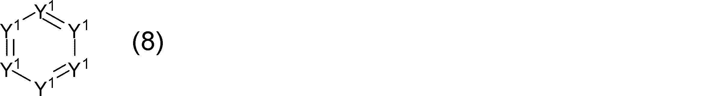
(前記一般式(8)において、Y1のうち2~4個は窒素原子であり、1つは、Lに結合する炭素原子であり、その他のY1は、CRyである。
一般式(8)が複数のRyを有する場合、Ryは、それぞれ独立して、
水素原子、
フッ素原子、
シアノ基、
ニトロ基、
置換もしくは無置換の環形成炭素数6~30のアリール基、
置換もしくは無置換の環形成原子数5~30の複素環基、
置換もしくは無置換の炭素数1~30のアルキル基、
置換もしくは無置換の炭素数1~30のアルキルカルボニル基、
置換もしくは無置換の環形成炭素数6~30のアリールカルボニル基、
置換もしくは無置換の炭素数1~30のアルキルスルフィニル基、
置換もしくは無置換の環形成炭素数6~30のアリールスルフィニル基、
置換もしくは無置換の炭素数2~60のアルキルホスフィニル基、
置換もしくは無置換の環形成炭素数6~60のアリールホスフィニル基、
置換もしくは無置換の炭素数1~30のアルキルスルホニル基、
置換もしくは無置換の環形成炭素数6~30のアリールスルホニル基、
置換もしくは無置換の炭素数3~60のアルキルシリル基、
置換もしくは無置換の環形成炭素数8~60のアリールシリル基、
置換もしくは無置換の炭素数1~30のアルコキシ基、または、
置換もしくは無置換の環形成炭素数6~30のアリールオキシ基である。
隣接する2つのY1がCRyであるとき、隣接する2つのY1が飽和または不飽和の環構造を形成していてもよい。)

(前記一般式(9)において、Y2は前記一般式(8)におけるその他のY1と同義である。)
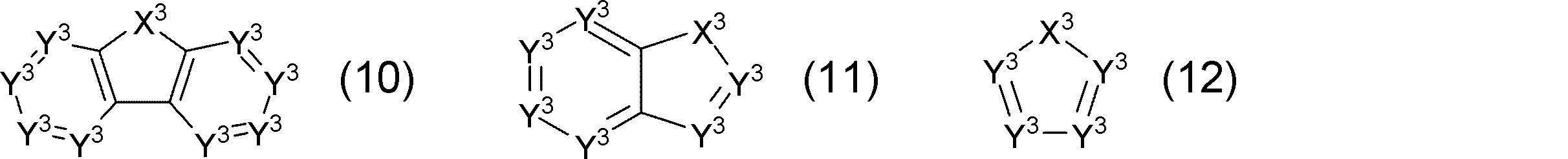
(前記一般式(10),(11),(12)において、
Y3は前記一般式(8)におけるその他のY1と同義である。
X3は下記一般式(41)~(45)から選ばれる連結基のいずれかを表す。)
Y3は前記一般式(8)におけるその他のY1と同義である。
X3は下記一般式(41)~(45)から選ばれる連結基のいずれかを表す。)

(前記一般式(43)~(45)において、
Rxは、それぞれ独立に、
水素原子、
置換もしくは無置換の炭素数6~30のアリール基、
置換もしくは無置換の環形成原子数5~30の複素環基または
置換もしくは無置換の炭素数1~30のアルキル基である。
複数のRxが存在する場合は互いに同じまたは異なる。)
Rxは、それぞれ独立に、
水素原子、
置換もしくは無置換の炭素数6~30のアリール基、
置換もしくは無置換の環形成原子数5~30の複素環基または
置換もしくは無置換の炭素数1~30のアルキル基である。
複数のRxが存在する場合は互いに同じまたは異なる。)
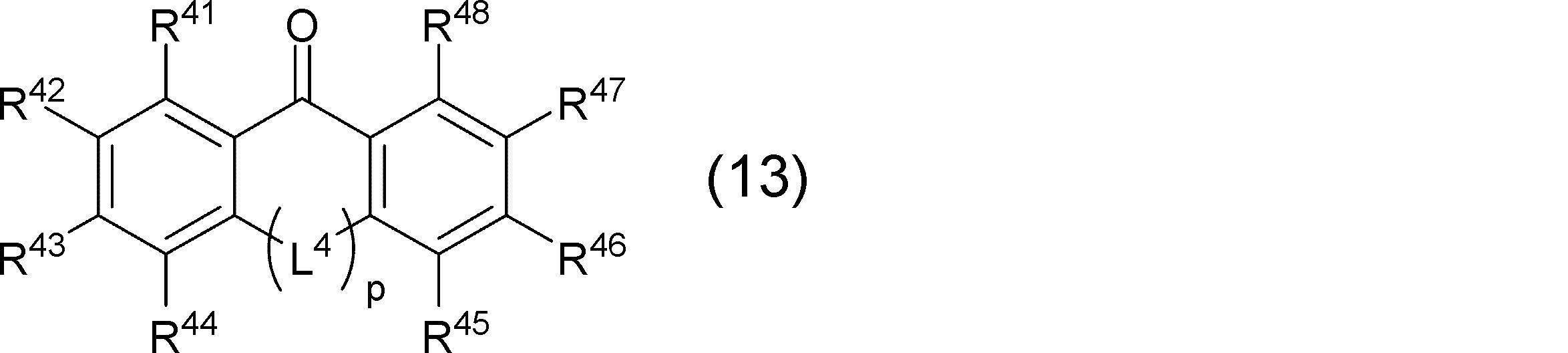
(前記一般式(13)において、
R41~R48のうち一つはLに対して結合する単結合であり、
その他のR41~R48は、前記一般式(8)におけるRyと同義である。
L4は下記一般式(131)~(136)から選ばれる連結基のいずれかを表す。
pは1~3の整数を表し、pが2または3の場合、複数のL4は互いに同じまたは異なる。)
R41~R48のうち一つはLに対して結合する単結合であり、
その他のR41~R48は、前記一般式(8)におけるRyと同義である。
L4は下記一般式(131)~(136)から選ばれる連結基のいずれかを表す。
pは1~3の整数を表し、pが2または3の場合、複数のL4は互いに同じまたは異なる。)
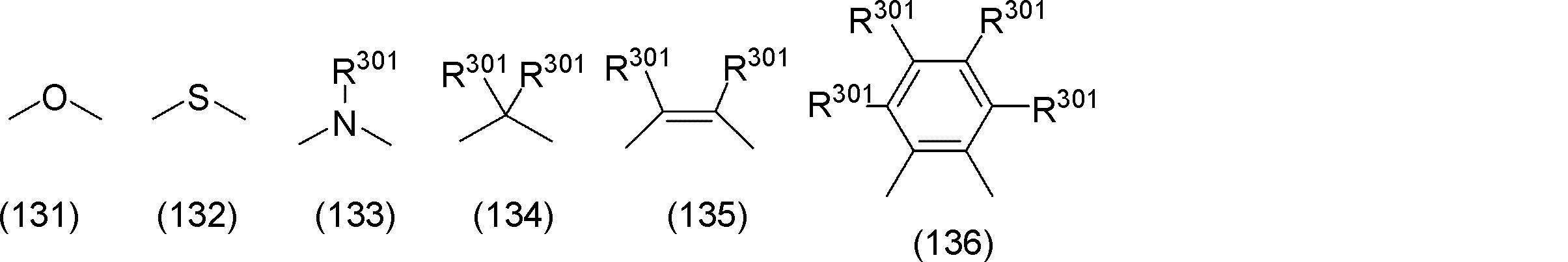
(前記一般式(133)~(136)において、
R301は、それぞれ独立に、
水素原子、
置換もしくは無置換の環形成炭素数6~30のアリール基、
置換もしくは無置換の環形成原子数5~30の複素環基、または
置換もしくは無置換の炭素数1~30のアルキル基である。
複数のR301が存在する場合は互いに同じまたは異なる。)
R301は、それぞれ独立に、
水素原子、
置換もしくは無置換の環形成炭素数6~30のアリール基、
置換もしくは無置換の環形成原子数5~30の複素環基、または
置換もしくは無置換の炭素数1~30のアルキル基である。
複数のR301が存在する場合は互いに同じまたは異なる。)
(前記一般式(14)において、
Araは、
置換もしくは無置換の環形成炭素数6~30のアリール基、または、
置換もしくは無置換の環形成原子数5~30の複素環基である。
Zaは、
フッ素原子、
シアノ基、
ニトロ基、
置換もしくは無置換の炭素数1~20のアルキルカルボニル基、
置換もしくは無置換の環形成炭素数6~30のアリールカルボニル基、
置換もしくは無置換の炭素数1~20のアルキルスルフィニル基、
置換もしくは無置換の環形成炭素数6~30のアリールスルフィニル基、
置換もしくは無置換の炭素数2~60のアルキルホスフィニル基、
置換もしくは無置換の環形成炭素数6~60のアリールホスフィニル基、
置換もしくは無置換の炭素数1~30のアルキルスルホニル基、または、
置換もしくは無置換の環形成炭素数6~30のアリールスルホニル基である。
qは、Araに直接結合するZaの置換数を表す1~5の整数であり、
qが2以上の場合、複数のZaは、互いに同一または異なる。)
Araは、
置換もしくは無置換の環形成炭素数6~30のアリール基、または、
置換もしくは無置換の環形成原子数5~30の複素環基である。
Zaは、
フッ素原子、
シアノ基、
ニトロ基、
置換もしくは無置換の炭素数1~20のアルキルカルボニル基、
置換もしくは無置換の環形成炭素数6~30のアリールカルボニル基、
置換もしくは無置換の炭素数1~20のアルキルスルフィニル基、
置換もしくは無置換の環形成炭素数6~30のアリールスルフィニル基、
置換もしくは無置換の炭素数2~60のアルキルホスフィニル基、
置換もしくは無置換の環形成炭素数6~60のアリールホスフィニル基、
置換もしくは無置換の炭素数1~30のアルキルスルホニル基、または、
置換もしくは無置換の環形成炭素数6~30のアリールスルホニル基である。
qは、Araに直接結合するZaの置換数を表す1~5の整数であり、
qが2以上の場合、複数のZaは、互いに同一または異なる。)
一般式(8)~(14)において、環形成炭素数6~30のアリール基、環形成原子数5~30の複素環基、および炭素数1~30のアルキル基、炭素数3~60のアルキルシリル基、環形成炭素数8~30のアリールシリル基、炭素数1~30のアルコキシ基、および環形成炭素数6~30のアリールオキシ基としては、上述した一般式(1)ならびに(b-1)~(b-2)および一般式(2)~(6)において説明した基が挙げられる。
炭素数1~30のアルキルカルボニル基は、-COORVと表される。
環形成炭素数6~30のアリールカルボニル基は、-COORWと表される。
炭素数1~30のアルキルスルフィニル基は、-S(=O)RVと表される。
環形成炭素数6~30のアリールスルフィニル基は、-S(=O)RWと表される。
炭素数2~40のアルキルホスフィニル基は、-P(=O)HRV、または-P(=O)(RV)2と表される。
環形成炭素数6~30のアリールホスフィニル基は、-P(=O)HRW、または-P(=O)(RW)2と表される。
炭素数1~30のアルキルスルホニル基は、-S(=O)2RVと表される。
環形成炭素数6~30のアリールスルホニル基は、-S(=O)2RWと表される。
これらの基において、RVの例としては、上記炭素数1~30のアルキル基が挙げられる。RWの例としては、上記環形成炭素数6~30のアリール基が挙げられる。環形成炭素数6~30のアリール基としては、フェニル基、ビフェニル基、ターフェニル基、トリフェニレニル基が好ましい。
前記一般式(1)で表される第1の材料としては、分子内でドナー要素とアクセプター要素とを結合した化合物となる観点から下記一般式(101)で表されるビスカルバゾール誘導体が好ましい。

上記一般式(101)において、A1及びA2は、互いに独立して、
水素原子、
ハロゲン原子、
シアノ基、
置換もしくは無置換の環形成炭素数6~30のアリール基、
置換もしくは無置換の環形成原子数5~30の複素環基、
置換もしくは無置換の炭素数1~30のアルキル基、
置換もしくは無置換の炭素数1~30のアルコキシ基、
置換もしくは無置換の炭素数7~30のアラルキル基、
置換もしくは無置換の環形成炭素数6~30のアリールオキシ基、
置換もしくは無置換の炭素数3~60のアルキルシリル基、または
置換もしくは無置換の環形成炭素数8~30のアリールシリル基を表す。
但し、A1及びA2の少なくとも1つは、シアノ基であることが好ましい。
水素原子、
ハロゲン原子、
シアノ基、
置換もしくは無置換の環形成炭素数6~30のアリール基、
置換もしくは無置換の環形成原子数5~30の複素環基、
置換もしくは無置換の炭素数1~30のアルキル基、
置換もしくは無置換の炭素数1~30のアルコキシ基、
置換もしくは無置換の炭素数7~30のアラルキル基、
置換もしくは無置換の環形成炭素数6~30のアリールオキシ基、
置換もしくは無置換の炭素数3~60のアルキルシリル基、または
置換もしくは無置換の環形成炭素数8~30のアリールシリル基を表す。
但し、A1及びA2の少なくとも1つは、シアノ基であることが好ましい。
上記一般式(101)において、Y11~Y14およびY23~Y26は、互いに独立して、C(R)または窒素原子を表し、Y15~Y18は、互いに独立して、C(R)、窒素原子またはY19~Y22のいずれかと結合する炭素原子を表し、Y19~Y22は、互いに独立して、C(R)、窒素原子またはY15~Y18のいずれかと結合する炭素原子を表し、Rは、それぞれ独立に、水素原子または置換基を表す。Rにおける置換基は、上述のA1およびA2が置換基を有する場合の置換基と同義である。
上記一般式(101)において、L1及びL2は、互いに独立して、単結合、置換もしくは無置換の環形成炭素数6~30の2価の芳香族炭化水素基、置換もしくは無置換の環形成原子数5~30の2価の複素環基、または当該2価の芳香族炭化水素基および当該2価の複素環基が連結した基を表す。
また、前記L1及び前記L2の少なくとも一方が、下記一般式(a)で表されることが好ましい。
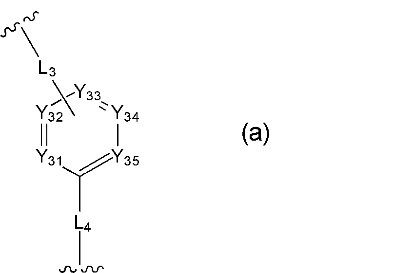
上記一般式(a)において、Y31~Y35は、互いに独立して、C(Ra)、窒素原子またはL3と結合する炭素原子を表し、
Raは、それぞれ独立に、水素原子又は置換基を表す。Raにおける置換基は、上述のA1およびA2が置換基を有する場合の置換基と同義である。
上記一般式(a)において、L3及びL4は、互いに独立して
単結合、
置換もしくは無置換の環形成炭素数6~30の2価の芳香族炭化水素基、
置換もしくは無置換の環形成原子数5~30の2価の複素環基、または
当該2価の芳香族炭化水素基および当該2価の複素環基が連結した基を表す。
Raは、それぞれ独立に、水素原子又は置換基を表す。Raにおける置換基は、上述のA1およびA2が置換基を有する場合の置換基と同義である。
上記一般式(a)において、L3及びL4は、互いに独立して
単結合、
置換もしくは無置換の環形成炭素数6~30の2価の芳香族炭化水素基、
置換もしくは無置換の環形成原子数5~30の2価の複素環基、または
当該2価の芳香族炭化水素基および当該2価の複素環基が連結した基を表す。
前記一般式(101)において、環形成炭素数6~30のアリール基、環形成原子数5~30の複素環基、および炭素数1~30のアルキル基、炭素数1~30のアルコキシ基、および環形成炭素数6~30のアリールオキシ基、炭素数3~60のアルキルシリル基、および環形成炭素数8~30のアリールシリル基としては、上述した一般式(1)ならびに(b-1)~(b-2)および一般式(2)~(6)において説明した基が挙げられる。
前記一般式(101)において、炭素数7~30のアラルキル基としては、後述する一般式(20)における炭素数7~30のアラルキル基において説明する基が挙げられる。
前記一般式(101)において、炭素数7~30のアラルキル基としては、後述する一般式(20)における炭素数7~30のアラルキル基において説明する基が挙げられる。
前記一般式(a)において、2価の芳香族炭化水素基としては、前記一般式(1)および(b-1)~(b-6)におけるアリール基から誘導される2価の基が挙げられる。また、前記一般式(a)において、環形成原子数5~30の2価の複素環基としては、前記一般式(1)および(b-1)~(b-6)における複素環基から誘導される2価の基が挙げられる。
前記一般式(1)で表される化合物としては、特に、Aが前記一般式(14)で表され、Bが前記一般式(2)で表され、Lが置換もしくは無置換の環形成炭素数6~30のアリール基であるものが好ましい。さらに、Lは、フェニレン基であることが好ましい。
本発明において、「環形成炭素」とは飽和環、不飽和環、又は芳香環を構成する炭素原子を意味する。「環形成原子」とはヘテロ環(飽和環、不飽和環、および芳香環を含む)を構成する炭素原子およびヘテロ原子を意味する。
また、「置換もしくは無置換の」という場合における置換基としては、上述のようなアリール基、複素環基、アルキル基(直鎖または分岐鎖のアルキル基、シクロアルキル基、ハロゲン化アルキル基)、アルケニル基、アルキニル基、アルキルシリル基、アリールシリル基、アルコキシ基、ハロゲン化アルコキシ基、アラルキル基、アリールオキシ基、ハロゲン原子、シアノ基に加え、ヒドロキシル基、ニトロ基、カルボキシ基等が挙げられる。ここで挙げた置換基の中では、アリール基、複素環基、アルキル基、ハロゲン原子、アルキルシリル基、アリールシリル基、シアノ基が好ましく、さらには、各置換基の説明において好ましいとした具体的な置換基が好ましい。「置換もしくは無置換の」という場合における「無置換」とは、前記置換基で置換されておらず、水素原子が結合していることを意味する。 以下に説明する化合物またはその部分構造において、「置換もしくは無置換の」という場合置換基についても、上記と同様である。 また、本発明において、水素原子とは、中性子数の異なる同位体、すなわち、軽水素(Protium)、重水素(Deuterium)、三重水素(Tritium)を包含する。
・ドーパント材料
本発明では、上記のとおり、発光層のドーパント材料に蛍光発光性のドーパント材料を用いる。
蛍光発光性のドーパント材料としては、公知の蛍光発光性材料を用いることができる。具体的には、例えば、ビスアリールアミノナフタレン誘導体、アリール置換ナフタレン誘導体、ビスアリールアミノアントラセン誘導体、アリール基置換アントラセン誘導体、ビスアリールアミノピレン誘導体、アリール基置換ピレン誘導体、ビスアリールアミノクリセン誘導体、アリール置換クリセン誘導体、ビスアリールアミノフルオランテン誘導体、アリール置換フルオランテン誘導体、インデノペリレン誘導体、ピロメテンホウ素錯体化合物、ピロメテン骨格を有する化合物もしくはその金属錯体、ジケトピロロピロール誘導体、ペリレン誘導体が挙げられる。
上記ドーパント材料のうち、特に、下記一般式(20)で表されるドーパント材料が好ましい。

(前記一般式(20)において、
Ar0は、置換もしくは無置換の環形成炭素数10~50の2価の縮合芳香族炭化水素基であり、
Ar1~Ar4は、それぞれ独立に、
置換もしくは無置換の環形成炭素数6~30のアリール基、
置換もしくは無置換の環形成原子数5~30の複素環基、
置換もしくは無置換の炭素数6~30のアルキル基、または、
置換もしくは無置換の炭素数7~50のアラルキル基である。)
Ar0は、置換もしくは無置換の環形成炭素数10~50の2価の縮合芳香族炭化水素基であり、
Ar1~Ar4は、それぞれ独立に、
置換もしくは無置換の環形成炭素数6~30のアリール基、
置換もしくは無置換の環形成原子数5~30の複素環基、
置換もしくは無置換の炭素数6~30のアルキル基、または、
置換もしくは無置換の炭素数7~50のアラルキル基である。)
上記一般式(20)における環形成炭素数10~50の2価の縮合芳香族炭化水素基としては、ナフチレン基、アントラセニレン基、フェナントリレン基、クリセニレン基、ピレニレン基、ベンゾアントラセニレン基、フルオランテニレン基、ベンゾフルオランテニレン基、ペリレニレン基、コロネリレン基、ピセニレン基、ジフェニルアントラセニレン基、フルオレニレン基、トリフェニリレン基、ルビセニレン基、フェニルアントラセニレン基、ビスアントラセニレン基、ジアントラセニルベンジニレン基、ジベンゾアントラセニレン基等が挙げられ、ナフチレン基、アントラセニレン基、フェナントリレン基、クリセニレン基、ピレニレン基、ベンゾアントラセニレン基が好ましい。
上記一般式(20)における炭素数6~30のアリール基、環形成原子数5~30の複素環基、炭素数6~30のアルキル基としては、上述した一般式(1)および(b-1)~(b-6)で説明した基が挙げられる。
上記一般式(20)における炭素数7~30のアラルキル基は、-Rv-Rwと表される。このRvの例として、上記炭素数1~30のアルキル基に対応するアルキレン基が挙げられる。このRwの例として、上記環形成炭素数6~30のアリール基の例が挙げられる。このアラルキル基は、炭素数7~30アラルキル基(アリール部分は炭素数6~30、好ましくは6~20、より好ましくは6~12)、アルキル部分は炭素数1~30(好ましくは1~20、より好ましくは1~10、さらに好ましくは1~6)であることが好ましい。このアラルキル基としては、例えば、ベンジル基、2-フェニルプロパン-2-イル基、1-フェニルエチル基、2-フェニルエチル基、1-フェニルイソプロピル基、2-フェニルイソプロピル基、フェニル-t-ブチル基、α-ナフチルメチル基、1-α-ナフチルエチル基、2-α-ナフチルエチル基、1-α-ナフチルイソプロピル基、2-α-ナフチルイソプロピル基、β-ナフチルメチル基、1-β-ナフチルエチル基、2-β-ナフチルエチル基、1-β-ナフチルイソプロピル基、2-β-ナフチルイソプロピル基、1-ピロリルメチル基、2-(1-ピロリル)エチル基、p-メチルベンジル基、m-メチルベンジル基、o-メチルベンジル基、p-クロロベンジル基、m-クロロベンジル基、o-クロロベンジル基、p-ブロモベンジル基、m-ブロモベンジル基、o-ブロモベンジル基、p-ヨードベンジル基、m-ヨードベンジル基、o-ヨードベンジル基、p-ヒドロキシベンジル基、m-ヒドロキシベンジル基、o-ヒドロキシベンジル基、p-アミノベンジル基、m-アミノベンジル基、o-アミノベンジル基、p-ニトロベンジル基、m-ニトロベンジル基、o-ニトロベンジル基、p-シアノベンジル基、m-シアノベンジル基、o-シアノベンジル基、1-ヒドロキシ-2-フェニルイソプロピル基、1-クロロ-2-フェニルイソプロピル基が挙げられる。
上記一般式(20)のAr1~Ar4の少なくとも1つは、下記一般式(21)で表されることが好ましい。
(前記一般式(21)において、
nは0~3、mは0~5、lは0~7の整数であり、
Xは酸素原子、硫黄原子又はセレン原子であり、
Arは、置換もしくは無置換の環形成炭素数6~30のアリーレン基、
Rは、
ハロゲン原子、
シアノ基、
ニトロ基、
ヒドロキシル基、
シリル基、
カルボキシル基、
置換もしくは無置換の環形成炭素数6~30のアリール基、
置換もしくは無置換の炭素数1~30のアルキル基、
置換もしくは無置換の炭素数1~30のアルキルアミノ基、
置換もしくは無置換の環形成炭素数6~60のアリールアミノ基、 置換もしくは無置換の炭素数1~30のアルコキシ基、
置換もしくは無置換の環形成炭素数6~30のアリールオキシ基、
置換もしくは無置換の環形成炭素数6~30のアリールチオ基、または、
置換もしくは無置換の炭素数1~30のアルコキシカルボニル基である。
また、n、m、lが2以上の場合、複数のAr及びRは、それぞれ同一または異なる。
Rが複数の場合、互いに結合して、飽和もしくは不飽和の、置換されていてもよい5員環または6員環の環状構造を形成してもよい。
前記一般式(21)において、環形成炭素数6~30のアリール基、炭素数1~30のアルキル基、炭素数1~30のアルキルアミノ基、環形成炭素数6~60のアリールアミノ基、炭素数1~30のアルコキシ基、環形成炭素数6~30のアリールオキシ基、および環形成炭素数6~30のアリールチオ基としては、上述した一般式(2)~(6),(51)において説明した基が挙げられる。
炭素数1~30のアルコキシカルボニル基は-COORVと表され、このRVの例として、上記炭素数1~30のアルキル基と同様のものが挙げられる。
炭素数1~30のアルコキシカルボニル基は-COORVと表され、このRVの例として、上記炭素数1~30のアルキル基と同様のものが挙げられる。
発光層の膜厚は、好ましくは5nm以上50nm以下、より好ましくは7nm以上50nm以下、最も好ましくは10nm以上50nm以下である。5nm未満では発光層形成が困難となり、色度の調整が困難となるおそれがあり、50nmを超えると駆動電圧が上昇するおそれがある。
発光層において、ホスト材料と蛍光発光性ドーパント材料との比率は、質量比で99:1以上50:50以下であることが好ましい。
さらに、前述したホスト材料、及びドーパント材料は以下の特定の条件を満たす化合物であることが好ましい。この特定の条件について、次に説明する。
ホスト材料の一重項エネルギーEgS(H)とドーパント材料の一重項エネルギーEgS(D)とが、下記数式(1)の関係を満たし、ホスト材料は、一重項エネルギーEgS(H)と、77[K]におけるエネルギーギャップEg77K(H)との差ΔST(H)が、下記数式(2)の関係を満たすことが好ましい。
なお、Eg77Kは、測定値であって、発光材料の試料を低温(77[K])で燐光スペクトル(縦軸:燐光発光強度、横軸:波長とする。)を測定し、この燐光スペクトルの短波長側の立ち上がりに対して接線を引き、その接線と横軸との交点の波長値に基づいて、所定の換算式から算出されるエネルギー量をエネルギーギャップのことである。
さらに、ホスト材料の77[K]におけるエネルギーギャップEg77K(H)と、ドーパント材料の77[K]におけるエネルギーギャップEg77K(T)との差ΔTが、下記数式(3)の関係を満たすことが好ましい。
・ΔST
ホスト材料として、一重項エネルギーEgSと三重項エネルギーEgTとのエネルギー差(ΔST)が小さい化合物を用いると、高電流密度領域で有機EL素子が高効率で発光する。上記ΔST(H)は、ホスト材料のΔSTについて示すものである。
一重項エネルギーEgSと三重項エネルギーEgTの差に値するΔSTを小さくするには、量子化学的には、一重項エネルギーEgSと三重項エネルギーEgTにおける交換相互作用が小さいことで実現する。ΔSTと交換相互作用の関係性における物理的な詳細に関しては、例えば、
文献1:安達千波矢ら、有機EL討論会 第10回例会予稿集、S2-5,p11~12
文献2:徳丸克己、有機光化学反応論、東京化学同人出版、(1973)
に記載されている。このような材料は、量子計算により分子設計を行い合成することが可能であり、具体的には、LUMO、及びHOMOの電子軌道を重ねないように局在化させた化合物である。
本実施形態のホスト材料に用いるΔSTの小さな化合物の例としては、分子内でドナー要素とアクセプター要素とを結合した化合物であり、さらに電気化学的な安定性(酸化還元安定性)を考慮し、ΔSTが0eV以上0.3eV未満の化合物が挙げられる。
また、より好ましい化合物は、分子の励起状態で形成される双極子(ダイポール)が互いに相互作用し、交換相互作用エネルギーが小さくなるような会合体を形成する化合物である。本発明者らの検討によれば、このような化合物は、双極子(ダイポール)の方向がおおよそ揃い、分子の相互作用により、さらにΔSTが小さくなり得る。このような場合、ΔSTは、0eV以上0.2eV以下と極めて小さくなり得る。
・会合体
上述のように、一重項エネルギーEgSと三重項エネルギーEgTとのエネルギー差(ΔST)を小さくするには、会合体を形成することによっても可能である。ここでの会合体とは、単純な1分子だけの電子状態を反映したものではなく、数分子が物理的に接近したものである。複数の分子が接近した結果、複数の分子間における電子状態が混ざり、電子状態が変化することによりエネルギー準位が変化し、主に一重項エネルギーの値が減少することで、ΔSTの値が小さくなると考えられる。このような会合体形成によるΔSTの値の減少は、2分子が接近した事により電子状態が変化するDavydov splitting modelによっても説明することができる(図2参照)。このDavydov splitting modelで示されるように、2分子が物理的に接近する事で、1分子と異なる電子状態の変化が考えられる。励起一重項状態がS1‐m+、及びS1‐m-の2つの状態で存在し、励起三重項状態がT1‐m+、及びT1‐m-の2つの状態で存在する。この結果、エネルギー準位が低いS1‐m-、及びT1‐m-が存在する事により、S1‐m-とT1‐m-との差であるΔSTの大きさは、1分子での電子状態と比べて、小さくなる。
上記Davydov splitting modelについては、例えば、
文献3:J. Kang, et al, International Journal of Polymer
Science, Volume 2010,Article ID 264781,
文献4:M. Kasha, et al, Pure and Applied Chemistry,
Vol.11, pp371, 1965
文献5:S. Das, et al, J. Phys. Chem. B., vol.103, pp209, 1999
に記載されている。
また、本発明者らは薄膜中に会合体を形成しやすい化合物を用いることによって、励起一重項状態と励起三重項状態の副準位を利用し、結果的に薄膜中の分子や会合体による逆項間交差が促進される可能性を見出した。
例えば、フォトルミネッセンススペクトルの半値幅が大きい化合物は、当該化合物の薄膜内において会合体を形成し易いと考えられる。また、フォトルミネッセンススペクトルの半値幅の大きさと会合体の形成し易さとの関連性は、次のように推測できる。
会合体を形成せずに主として1分子状態で存在する性質の化合物については、励起一重項状態における振動準位の存在が少なく、その結果、フォトルミネッセンススペクトルの半値幅が狭く観測される。例えば、CBP(4,4’-bis[9-dicarbazolyl]-2,2’-biphenyl)は、主として1分子状態で存在する性質を有し、フォトルミネッセンススペクトルの半値幅の大きさは、50nm程度と比較的狭い。
一方、会合体を形成し易い化合物については、複数の分子が電子的に影響しあう事により、励起一重項状態に多くの振動準位が存在する。この結果、各振動準位から基底状態に緩和する状態が多くなるので、フォトルミネッセンススペクトルの半値幅が大きくなる。
このような会合体を形成しやすい化合物は、励起三重項状態においても多くの振動準位が存在すると予想される。その結果、励起一重項状態と励起三重項状態との間に副準位が多く存在することになるため、この副準位を介在して熱的なΔSTが小さくなり、逆項間交差が促進されると考えられる。
なお、本実施形態における会合体とは、単分子同士が任意の会合体を形成することを意味している。すなわち、特定の会合状態を示すものではない。有機分子の会合状態は、薄膜中では確率的に様々な状態を許容するものであり、無機分子とは大きくこの点を異にする。
・TADF機構
前述したとおり、有機材料のΔST(H)が小さいと、外部から与えられる熱エネルギーによって、ホスト材料の三重項準位からホスト材料の一重項準位への逆項間交差が起こり易くなる。ここで、有機EL素子内部の電気励起された励起子の励起三重項状態が、逆項間交差によって、励起一重項状態へスピン交換がされるエネルギー状態変換機構をTADF機構と呼ぶ。
本実施形態では、ホスト材料にΔST(H)が小さい化合物を用いるため、外部から与えられる熱エネルギーによって、ホスト材料の三重項準位からホスト材料の一重項準位への逆項間交差が起こり易くする。
図3は、発光層におけるホスト材料、及びドーパント材料のエネルギー準位の関係を示す図である。図3において、S0は、基底状態を表し、S1Hは、ホスト材料の最低励起一重項状態を表し、T1Hは、ホスト材料の最低励起三重項状態を表し、S1Dは、ドーパント材料の最低励起一重項状態を表し、T1Dは、ドーパント材料の最低励起三重項状態を表す。図3に示すように、S1HとT1Hとの差がΔST(H)に相当し、S1HとS0との差がEgS(H)に相当し、S1DとS0との差がEgS(D)に相当し、T1HとT1Dとの差がΔTに相当する。図3中の破線矢印は、各励起状態間のエネルギー移動を表す。
上記のとおり、本実施形態のホスト材料に用いる化合物として選択されるのは、ΔST(H)の小さい化合物である。何故なら、ΔST(H)の小さな材料では、最低励起三重項状態T1Hに生じた三重項励起子が熱エネルギーにより、ホスト材料の最低励起一重項状態S1Hに逆項間交差する現象が起こり易くなると考えられるからである。ΔST(H)が小さいため、例えば、室温程度でも逆項間交差が起こり易くなる。このような逆項間交差が起こり易くなれば、ホスト材料から蛍光発光性のドーパント材料の最低励起一重項状態T1Dへとフェルスター移動によりエネルギー移動する割合も増え、結果として蛍光型の有機EL素子の発光効率が向上する。
つまり、ホスト材料にΔST(H)が小さい化合物を用いることで、TADF機構に由来する発光が増え、結果として遅延蛍光比率が大きくなる。遅延蛍光比率が大きくなれば、高い内部量子効率を得ることができる。なお、このTADF機構による遅延蛍光を利用することにより、理論的に内部量子効率を100%まで高めることができると考えられる。
一方、図4は、特許文献1に記載のTADF機構における発光層のホスト材料、及びドーパント材料のエネルギー準位の関係を示すものである。図4において、S0、S1H、T1H、S1D、T1Dは、図3と同義であり、破線の矢印は、各励起状態間のエネルギー移動を表す。図4に示すように、非特許文献1に記載のTADF機構では、ドーパント材料としてΔST(D)の小さな材料を用いる。これにより、ホスト材料の最低励起三重項状態T1Hからのデクスター移動によりドーパント材料の最低励起三重項状態T1Dにエネルギー移動する。さらにドーパント材料の最低励起三重項状態T1Dは熱エネルギーにより、最低励起一重項状態S1Dに逆項間交差することが可能であり、この結果、ドーパント材料の最低励起一重項状態T1Dからの蛍光発光を観測することができる。このTADF機構による遅延蛍光を利用することによっても、理論的に内部効率を100%まで高めることができると考えられている。
ここで本発明者らは、非特許文献1に記載されるようなΔST(H)が小さい蛍光発光性化合物をホスト材料として、ホスト-ドーパントシステムに採用する。その理由は、以下に詳述する通りである。
第一に、ドーパント材料上でのTADF機構によるエネルギー状態の変換を考えた場合、ドーパント材料は蛍光発光をするため、比較的高い一重項エネルギーを有するとともに、同程度の三重項エネルギーを有することになる。該三重項エネルギーを発光層内に有効に閉じ込めるためには、より大きい三重項エネルギーを有するホスト材料を選択する必要がある。ここで、該ホスト材料に一般的にΔSTの大きい通常の有機材料を用いることになれば、該ホスト材料の一重項エネルギー、すなわちHOMO準位とLUMO準位のエネルギー差は非常に大きいものとなる。この結果、該ホスト材料と、発光層に隣接するキャリア輸送層とのエネルギー差が大きくなるため、発光層へのキャリア注入が難しくなると考えられる。従って、本発明者らは、TADF機構によるエネルギー状態の変換は、ホスト材料上で行われるほうが好ましく、これによって発光層へのキャリア注入は有利になり、有機EL素子全体としてキャリアバランスが取りやすくなると考える。
第二に、ΔST(H)が小さい蛍光発光性化合物をホスト材料に用いることにより、高電流密度領域におけるTriplet-Triplet-Annihilationに起因する発光効率の低下を抑制することができると考える。ここでTriplet-Triplet-Annihilation(以下、TTAと呼ぶ)とは、分子上で生成した励起子寿命の長い三重項励起子が高密度で隣接することにより、励起子同士の衝突が起こって励起子が熱失活してしまう物理現象である。
本発明者らは、ホスト材料からドーパント材料へ三重項エネルギーが遷移しにくいホスト-ドーパントシステムにおいては、高電流密度領域における発光効率の低下をある程度抑制することができると考える。本実施形態では、ΔSTが小さい化合物を発光層のホスト材料に用いており、ホスト材料の三重項励起準位はTADF機構によって一重項励起準位へ逆項間交差後、ドーパント材料の一重項励起準位にエネルギー移動する。従って、生成された三重項励起子は、発光層中において存在比が大きいホスト材料上で三重項励状態が保たれることになる。一方、ΔSTが小さい化合物を発光層のドーパント材料に用いる場合、生成された三重項励起子は、発光層中において存在比が極めて小さいドーパント材料上で三重項励状態が保たれることになる。即ち、高電流領域の有機EL素子の駆動においては、三重項励起状態がドーパント材料上に集中しないようなシステムを設計することが好ましいと考え、本発明ではΔST(H)が小さい化合物をホスト材料として採用する。
本発明者らは、ホスト材料からドーパント材料へ三重項エネルギーが遷移しにくいホスト-ドーパントシステムにおいては、高電流密度領域における発光効率の低下をある程度抑制することができると考える。本実施形態では、ΔSTが小さい化合物を発光層のホスト材料に用いており、ホスト材料の三重項励起準位はTADF機構によって一重項励起準位へ逆項間交差後、ドーパント材料の一重項励起準位にエネルギー移動する。従って、生成された三重項励起子は、発光層中において存在比が大きいホスト材料上で三重項励状態が保たれることになる。一方、ΔSTが小さい化合物を発光層のドーパント材料に用いる場合、生成された三重項励起子は、発光層中において存在比が極めて小さいドーパント材料上で三重項励状態が保たれることになる。即ち、高電流領域の有機EL素子の駆動においては、三重項励起状態がドーパント材料上に集中しないようなシステムを設計することが好ましいと考え、本発明ではΔST(H)が小さい化合物をホスト材料として採用する。
第三に、三重項準位から一重項準位への逆項間交差を起こす材料をホスト材料に採用することで、ドーパント材料に発光量子収率の高い材料を簡便に選択することができる。この結果、ドーパント材料にエネルギー移動した一重項励起子は速やかに発光緩和するので、高電流密度領域におけるエネルギークエンチの抑制が可能である。一般に、蛍光素子におけるホスト-ドーパントシステムでは、ホスト材料は、キャリア輸送機能と励起子生成機能とを有し、ドーパント材料は、発光機能を有する。これは、発光層におけるキャリア輸送機能と発光機能とを機能分離するものであって、発光量子収率の高いドーパント材料を発光層に少量ドーピングすることによって、効果的な有機EL発光を促すものである。本発明の発光層では、一般的な発光層の機能に加え、TADF機構による逆項間交差を引き起こす機能が求められる。本発明者らは、TADF機構による逆項間交差を引き起こす機能をホスト材料に求めることによって、有機EL素子の発光効率に大きく寄与する、高い発光量子収率を有するドーパント材料の選択性を増やした。これにより、従来から高効率として知られる蛍光発光性のドーパント材料を選択することができる。
・EgTとEg77Kとの関係
ここで、本実施形態ではΔSTが所定値以下である化合物を用いており、上記した三重項エネルギーEgTは、通常定義される三重項エネルギーとは異なる点がある。この点について、以下に説明する。
一般に、三重項エネルギーは、測定対象となる化合物を溶媒に溶解させた試料を低温(77[K])で燐光スペクトル(縦軸:燐光発光強度、横軸:波長とする。)を測定し、この燐光スペクトルの短波長側の立ち上がりに対して接線を引き、その接線と横軸との交点の波長値に基づいて、所定の換算式から算出される。
ここで、本発明のホスト材料に用いる化合物は、上記のとおりΔSTが小さい。ΔSTが小さいと、低温(77[K])状態でも、項間交差、及び逆項間交差が起こりやすく、励起一重項状態と励起三重項状態とが混在する。その結果、上記と同様にして測定されるスペクトルは、励起一重項状態、及び励起三重項状態の両者からの発光を含んだものとなり、いずれの状態から発光したものかについて峻別することは困難であるが、基本的には3重項エネルギーの値が支配的と考えられる。
そのため、本発明では、上記した三重項エネルギーEgTを、通常の三重項エネルギーEgTとその厳密な意味において異なることを区別するため、以下に示す2通りの測定方法によって測定されたものを示す。
[1-1]測定方法1のEgT
測定対象となる化合物を溶媒に溶解させた試料について低温(77[K])で燐光スペクトル(縦軸:燐光発光強度、横軸:波長とする。)を測定し、この燐光スペクトルの短波長側の立ち上がりに対して接線を引き、その接線と横軸との交点の波長値に基づいて、所定の換算式から算出されるエネルギー量をエネルギーギャップEg77Kとする。そして、ΔSTを、後述する測定方法1の一重項エネルギーEgSと本測定方法1のエネルギーギャップEg77Kとの差として定義する。それゆえ、ΔST(H)については、上記式(2)のように表されることが好ましい。
測定対象となる化合物を溶媒に溶解させた試料について低温(77[K])で燐光スペクトル(縦軸:燐光発光強度、横軸:波長とする。)を測定し、この燐光スペクトルの短波長側の立ち上がりに対して接線を引き、その接線と横軸との交点の波長値に基づいて、所定の換算式から算出されるエネルギー量をエネルギーギャップEg77Kとする。そして、ΔSTを、後述する測定方法1の一重項エネルギーEgSと本測定方法1のエネルギーギャップEg77Kとの差として定義する。それゆえ、ΔST(H)については、上記式(2)のように表されることが好ましい。
[1-2]測定方法2のEgT
測定対象となる化合物を石英基板上に蒸着して試料を作製し、膜厚を100nmとする。この試料について、低温(77[K])で燐光スペクトル(縦軸:燐光発光強度、横軸:波長とする。)を測定し、この燐光スペクトルの短波長側の立ち上がりに対して接線を引き、その接線と横軸との交点の波長値に基づいて、所定の換算式から算出されるエネルギー量をエネルギーギャップEg77Kとする。そして、ΔSTを後述する測定方法2の一重項エネルギーEgSと本測定方法2のエネルギーギャップEg77Kとの差として定義する。それゆえ、ΔST(H)については、上記式(2)のように表されることが好ましい。
測定対象となる化合物を石英基板上に蒸着して試料を作製し、膜厚を100nmとする。この試料について、低温(77[K])で燐光スペクトル(縦軸:燐光発光強度、横軸:波長とする。)を測定し、この燐光スペクトルの短波長側の立ち上がりに対して接線を引き、その接線と横軸との交点の波長値に基づいて、所定の換算式から算出されるエネルギー量をエネルギーギャップEg77Kとする。そして、ΔSTを後述する測定方法2の一重項エネルギーEgSと本測定方法2のエネルギーギャップEg77Kとの差として定義する。それゆえ、ΔST(H)については、上記式(2)のように表されることが好ましい。
溶液状態における三重項エネルギーの測定には、対象分子と溶媒との間における相互作用により三重項エネルギーに誤差を含む場合がある。そのため理想的な条件としては、対象分子と溶媒との相互作用を除くため、薄膜状態における測定が望まれる。しかしながら、本発明でホスト材料に用いられる化合物の分子は、溶液状態において幅広い半値幅を有するフォトルミネッセンススペクトルを示すことから、溶液状態においても会合状態を形成していることが強く示唆され、薄膜状態と同等の条件と考えられる。また、上記した通り、通常の三重項エネルギーEgTは溶液状態において測定される。したがって、本発明では、三重項エネルギーEg77Kについて、薄膜条件で測定した値とともに、比較のため溶液条件で測定した値も用いることにした。
・一重項エネルギーEgS
一重項エネルギーEgSについては、本発明においても通常の手法と同様にして算出されるもので定義される。一重項エネルギーEgSの定義としては、以下の2つを用いた。
[2-1]測定方法3のEgS
測定対象となる化合物を石英基板上に蒸着して試料を作製し、常温(300K)でこの試料の吸収スペクトル(縦軸:吸光度、横軸:波長とする。)を測定する。この吸収スペクトルの長波長側の立ち下がりに対して接線を引き、その接線と横軸との交点の波長値に基づいて、所定の換算式から算出される。
[2-2]測定方法4のEgS
測定対象となる化合物を石英基板上に蒸着して試料を作製し、常温(300K)でこの試料の発光スペクトル(縦軸:発光強度、横軸:波長とする。)を測定する。この発光スペクトルの短波長側の立ち上がりに対して接線を引き、その接線と横軸との交点の波長値に基づいて、所定の換算式から算出される。
なお、会合体を形成する場合の、EgSは、上記測定方法3および測定方法4のいずれにおいても、上記Davydov
splitting modelにおけるS1‐m-と基底状態S0とのエネルギーギャップに対応する。
一重項エネルギーEgS、及びエネルギーギャップEg77Kの具体的な算出については、後述する。 上記したように、本発明においては、エネルギーギャップEg77Kと一重項エネルギーEgSの定義が、それぞれ2つ存在する。そして、これらのEg77KおよびEgSから、2通りのΔSTが定義される。すなわち、測定方法1のエネルギーギャップEg77Kと測定方法3の一重厚エネルギーEgSにより定義されるΔSTと、測定方法2のエネルギーギャップEg77Kと測定方法4の一重項エネルギーEgSにより定義されるΔSTが存在する。本発明においては、少なくともいずれかの定義におけるΔSTが上記式(2)で表されることが好ましい。
・遅延蛍光比率
本発明の有機EL素子によれば、遅延蛍光の比率が、TTF機構のみで遅延蛍光が起こっていると仮定した場合の遅延蛍光の比率(TTF比率)の理論値上限を上回ることを見出した。つまり、本発明によれば、より高い内部量子効率の有機EL素子を実現することができる。
本発明の有機EL素子によれば、遅延蛍光の比率が、TTF機構のみで遅延蛍光が起こっていると仮定した場合の遅延蛍光の比率(TTF比率)の理論値上限を上回ることを見出した。つまり、本発明によれば、より高い内部量子効率の有機EL素子を実現することができる。
遅延蛍光比率は、過渡EL法により測定することができる。過渡EL法とは、素子に印加しているパルス電圧を除去した後のEL発光の減衰挙動(過渡特性)を測定する手法である。EL発光強度は、最初の再結合で生成する一重項励起子からの発光成分と、三重項励起子を経由して生成する一重項励起子からの発光成分に分類される。最初の再結合で生成する一重項励起子の寿命はナノ秒オーダーであり非常に短いためパルス電圧除去後、速やかに減衰する。
一方、遅延蛍光は寿命の長い三重項励起子を経由して生成する一重項励起子からの発光のため、ゆるやかに減衰する。このように最初の再結合で生成する一重項励起子からの発光と三重項励起子を経由して生成する一重項励起子からの発光は時間的に大きな差があるため、遅延蛍光由来の発光強度を求めることができる。具体的には以下の方法により決定することができる。
過渡EL波形は以下のようにして測定する(図5参照)。電圧パルスジェネレータ(PG)11から出力されるパルス電圧波形を有機EL素子(EL)12に印加する。印加電圧波形をオシロスコープ(OSC)13に取り込む。パルス電圧を有機EL素子12に印加すると、有機EL素子12はパルス発光を生じる。この発光を、光電子増倍管(PMT)14を経由してオシロスコープ(OSC)13に取り込む。電圧波形とパルス発光を同期させてパーソナルコンピュータ(PC)15に取り込む。
過渡EL波形の解析により、遅延蛍光由来の発光強度比を以下のようにして定義する。なお、遅延蛍光由来の発光強度比を算出するのに、国際公開第2010/134352号に記載されるTTF比率の算出式を用いることができる。
ただし、本発明で定義される遅延蛍光成分とは、TTF由来の発光成分に加え、本発明が開示する熱活性化による遅延蛍光(TADF機構)が含まれると考えられる。従って、本発明では、以下の数式(4)から求められる遅延蛍光成分の比率をTTF比率とは呼ばず、遅延蛍光比率と呼ぶことにする。
遅延蛍光比率は、数式(4)を用いて求める。
ただし、本発明で定義される遅延蛍光成分とは、TTF由来の発光成分に加え、本発明が開示する熱活性化による遅延蛍光(TADF機構)が含まれると考えられる。従って、本発明では、以下の数式(4)から求められる遅延蛍光成分の比率をTTF比率とは呼ばず、遅延蛍光比率と呼ぶことにする。
遅延蛍光比率は、数式(4)を用いて求める。
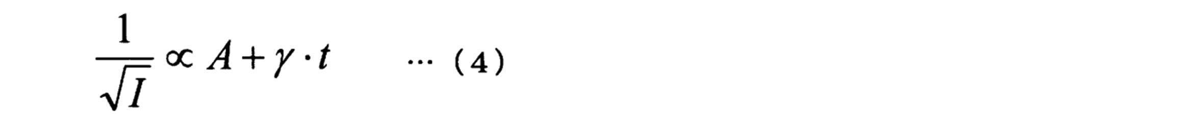
数式(4)中、Iは、遅延蛍光由来の発光強度であり、Aは、定数である。そこで、測定した過渡EL波形データを数式(4)でフィッティングし、定数Aを求める。このときパルス電圧を除去した時刻t=0における発光強度1/A2が遅延蛍光由来の発光強度比と定義する。
図6Aのグラフは、有機EL素子に所定のパルス電圧を印加し、その後電圧を除去した時の過渡EL波形の測定例であり、有機EL素子の発光強度の時間変化をあらわしたものである。
図6Aのグラフにて、時刻約3×10⁻⁸秒のところでパルス電圧を除去した。なお、図6Aのグラフは電圧を除去した時の輝度を1として表したものである。
電圧除去後、約2×10⁻⁷秒までの急速な減衰の後、緩やかな減衰成分が現れる。
図6Aのグラフにて、時刻約3×10⁻⁸秒のところでパルス電圧を除去した。なお、図6Aのグラフは電圧を除去した時の輝度を1として表したものである。
電圧除去後、約2×10⁻⁷秒までの急速な減衰の後、緩やかな減衰成分が現れる。
図6Bのグラフは、電圧除去時点を原点にとり、電圧除去後、1.5×10⁻⁵秒までの光強度の平方根の逆数をプロットしたグラフである。フィッティングは以下のように行う。
直線部分を時間原点へ延長したときの縦軸との交点Aの値は1.55である。すると、この過渡EL波形から得られる遅延蛍光由来の発光強度比は、1/(1.55)2=0.41となる。つまり、41%が遅延蛍光由来であることになる。すなわち、TTF比率の理論限界と考えられる37.5%を超えるものである。
過渡EL波形から得られる遅延蛍光由来の発光強度は、測定する温度により変化している。このような現象は、主にTADF機構による蛍光発光特有のものと考えられる。
直線へのフィッティングは、最小二乗法により行うことが好ましい。この場合、10-5秒までの値を用いてフィッティングすることが好ましい。
直線部分を時間原点へ延長したときの縦軸との交点Aの値は1.55である。すると、この過渡EL波形から得られる遅延蛍光由来の発光強度比は、1/(1.55)2=0.41となる。つまり、41%が遅延蛍光由来であることになる。すなわち、TTF比率の理論限界と考えられる37.5%を超えるものである。
過渡EL波形から得られる遅延蛍光由来の発光強度は、測定する温度により変化している。このような現象は、主にTADF機構による蛍光発光特有のものと考えられる。
直線へのフィッティングは、最小二乗法により行うことが好ましい。この場合、10-5秒までの値を用いてフィッティングすることが好ましい。
ここで、遅延蛍光による発光メカニズムを持つTTF機構について、図7を用いて説明する。図7は、TTF機構を利用した有機EL素子におけるホスト材料、及びドーパント材料のエネルギー準位の関係を示したものである。図7において、S0、S1H、T1H、S1D、T1Dは、図3と同義である。図7において、矢印は、各励起状態間のエネルギー移動を表す。
上記したように、TTF機構は、2つの三重項励起子の衝突によって、一重項励起子が生成する現象を利用するものである。図7に示すように、ホスト材料の最低励起三重項状態T1Hは、ドーパント材料の最低励起三重項状態T1Dよりも小さいことが好ましいとされ、この結果、三重項励起子はホスト材料分子上に集中する。これらの三重項励起子の密度が高まることで三重項励起子同士が効率的に対衝突を起していき、一部は一重項励起子に変化することになる。TTF機構によって生成されたホスト材料の最低励起一重項状態S1Hは速やかにドーパント材料の最低励起一重項状態S1Dへのフェルスター移動を起こし、ドーパント材料が蛍光発光をする。
上記したように、TTF機構は、2つの三重項励起子の衝突によって、一重項励起子が生成する現象を利用するものである。図7に示すように、ホスト材料の最低励起三重項状態T1Hは、ドーパント材料の最低励起三重項状態T1Dよりも小さいことが好ましいとされ、この結果、三重項励起子はホスト材料分子上に集中する。これらの三重項励起子の密度が高まることで三重項励起子同士が効率的に対衝突を起していき、一部は一重項励起子に変化することになる。TTF機構によって生成されたホスト材料の最低励起一重項状態S1Hは速やかにドーパント材料の最低励起一重項状態S1Dへのフェルスター移動を起こし、ドーパント材料が蛍光発光をする。
なお、TTF比率の理論値上限は、次のようにして求めることができる。
S.M.Bachiloらによれば(J.Phys.Cem.A,104,7711(2000))、五重項等の高次の励起子が、すぐに三重項に戻ると仮定すると、三重項励起子(以下、3A*と記載する)の密度が上がってきたとき、三重項励起子同士が衝突し下記数式(5)のような反応が起きる。ここで、1Aは基底状態、1A*は最低励起一重項励起子を表す。
S.M.Bachiloらによれば(J.Phys.Cem.A,104,7711(2000))、五重項等の高次の励起子が、すぐに三重項に戻ると仮定すると、三重項励起子(以下、3A*と記載する)の密度が上がってきたとき、三重項励起子同士が衝突し下記数式(5)のような反応が起きる。ここで、1Aは基底状態、1A*は最低励起一重項励起子を表す。
すなわち、
53A*→41A+1A*
となり、当初生成した75%の三重項励起子のうち、1/5、つまり20%が一重項励起子に変化することが予測されている。
従って、光として寄与する一重項励起子は、当初生成する25%分に75%×(1/5)=15%を加えた40%ということになる。
このとき、全発光強度中に占めるTTF由来の発光比率(TTF比率)は、15/40、すなわち37.5%となる。よって、本発明の有機EL素子の遅延蛍光比率は、TTF比率のみの理論値上限を上回ることが分かる。
53A*→41A+1A*
となり、当初生成した75%の三重項励起子のうち、1/5、つまり20%が一重項励起子に変化することが予測されている。
従って、光として寄与する一重項励起子は、当初生成する25%分に75%×(1/5)=15%を加えた40%ということになる。
このとき、全発光強度中に占めるTTF由来の発光比率(TTF比率)は、15/40、すなわち37.5%となる。よって、本発明の有機EL素子の遅延蛍光比率は、TTF比率のみの理論値上限を上回ることが分かる。
・1μsにおける残存強度比
遅延蛍光の大きさを相対的に知る方法としては、1μsにおける残存強度を測定することが挙げられる。1μsにおける残存強度比は、過渡EL法により測定したパルス電圧を除去した時点における発光強度に対する、パルス電圧を除去したのち1μs経過後の発光強度の比と定義する。過渡EL法により測定したパルス電圧を除去した後のEL発光の減衰挙動から、相対的な遅延蛍光の量を見積もることができる。1μsにおける残存強度比は、図6Aのグラフにおける1.0μs時の発光強度を読み取ることにより取得できる。
なお、1μsにおける残存強度比は、36.0%より大きいことが好ましい。さらに好ましくは、38.0%以上である。
遅延蛍光の大きさを相対的に知る方法としては、1μsにおける残存強度を測定することが挙げられる。1μsにおける残存強度比は、過渡EL法により測定したパルス電圧を除去した時点における発光強度に対する、パルス電圧を除去したのち1μs経過後の発光強度の比と定義する。過渡EL法により測定したパルス電圧を除去した後のEL発光の減衰挙動から、相対的な遅延蛍光の量を見積もることができる。1μsにおける残存強度比は、図6Aのグラフにおける1.0μs時の発光強度を読み取ることにより取得できる。
なお、1μsにおける残存強度比は、36.0%より大きいことが好ましい。さらに好ましくは、38.0%以上である。
・ドーパントの特性
本実施形態における好ましいドーパント材料の特性としては、蛍光発光性で、かつ輻射遷移の速度定数が大きいものである。このような場合、ホスト材料で電気励起された一重項励起子及び、TADF機構によって生成された一重項励起子等は、ドーパント材料の一重項励起子にフェルスターエネルギー移動し、ドーパント材料は速やかに発光する。即ち、ホスト材料上の三重項励起子がTTAを起こす前に、上記エネルギー遷移を経て蛍光発光することが可能となり、高電流領域の効率低下が大きく改善される可能性がある。
本実施形態における輻射遷移の速度定数が大きいドーパント材料は、ドーパント材料の蛍光寿命が、5ns以下となるものを選択することが好ましい。さらに好ましくは、2ns以下であることである。また、ドーパント材料の蛍光量子収率は、溶液状態で80%以上であることが好ましい。蛍光量子収率は、例えば、浜松ホトニクス(株)製、絶対PL量子収率測定装置 C9920-02を用い、トルエン溶液中の濃度が10-5mol/l~10-6mol/lの範囲で測定することによって求めることができる。
また、輻射遷移の速度定数の大きいドーパント材料であることは、素子のELスペクトルを測定し、ドーパント材料の発光成分に対し、それ以外の発光成分が1/10以下であることを確認することからも推定される。
・発光層と電子輸送層との関係
また、ホスト材料のΔST(H)が小さいと、ホスト材料と、発光層に隣接する電子輸送層とのエネルギー差が小さくなり、発光層に電子が注入しやすくなる。その結果、キャリアバランスが取りやすくなり、ロールオフが小さくなる
また、ホスト材料のΔST(H)が小さいと、ホスト材料と、発光層に隣接する電子輸送層とのエネルギー差が小さくなり、発光層に電子が注入しやすくなる。その結果、キャリアバランスが取りやすくなり、ロールオフが小さくなる
・発光層と正孔輸送層との関係
また、正孔輸送層のイオン化ポテンシャルをIPHTとしたとき、IPHT≦5.7eVであることが好ましい。これにより、電子と正孔とのバランスをより整えることが可能となる。イオン化ポテンシャルは、例えば、光電子分光装置(理研計器(株)製:AC-3)を用いて当該材料の薄膜状態で測定することによって求めることができる。
また、正孔輸送層のイオン化ポテンシャルをIPHTとしたとき、IPHT≦5.7eVであることが好ましい。これにより、電子と正孔とのバランスをより整えることが可能となる。イオン化ポテンシャルは、例えば、光電子分光装置(理研計器(株)製:AC-3)を用いて当該材料の薄膜状態で測定することによって求めることができる。
・ホスト材料とドーパント材料の一重項エネルギーの関係
本実施形態において、ドーパント材料は、蛍光発光性のドーパント材料であり、ホスト材料に用いる化合物とドーパント材料に用いる化合物は、前記数式(2)のような一重項エネルギーの大小関係を満たす。
このような関係を満たすことで、ホスト材料の当初生成する一重項励起子と遅延蛍光由来の一重項励起子が、ドーパント材料へエネルギー移動し易くなる。その結果、ドーパント材料が効率良く蛍光発光する。
本実施形態において、ドーパント材料は、蛍光発光性のドーパント材料であり、ホスト材料に用いる化合物とドーパント材料に用いる化合物は、前記数式(2)のような一重項エネルギーの大小関係を満たす。
このような関係を満たすことで、ホスト材料の当初生成する一重項励起子と遅延蛍光由来の一重項励起子が、ドーパント材料へエネルギー移動し易くなる。その結果、ドーパント材料が効率良く蛍光発光する。
・Δn
本発明者らは、ΔSTを小さくする手段の一つとして会合体を形成する化合物を用いることを見出し、Δnが大きい化合物は、当該化合物の膜内において会合体を形成し易いことを見出した。ここでのΔnとは、分光エリプソメトリー測定(測定範囲:200nm~1000nm)において屈折率と同時に観測される反射率が観測されない領域において、シリコン基板面に対して垂直方向の屈折率nZと、シリコン基板に対して平行方向の屈折率nXとの差が最も大きい時の値を取ったものである。
Δnの大きさと会合体の形成し易さとの関連性は、次のように推測される。
シリコン基板面に対して垂直方向zと平行方向xの屈折率nに大きな違いが生じる場合は、薄膜状態において分子が、ある程度の規則性を有する状態で存在していることを意味していると考えられる。すなわち、本発明のホスト材料に用いる化合物は、所定の大きさのΔnを有する化合物であり、薄膜状態において会合体を形成し、ある程度の規則性を有して存在していると推測される。
一方で、このΔnが非常に小さい化合物、例えば、CBPやAlq3(tris(8-hydroxyquinolinato)aluminium)などは、薄膜状態において分子が全く規則性を有していないアモルファス状態で存在している。
Δnの大きさと会合体の形成し易さとの関連性については、例えば、
文献6:D. Yokoyama et al., Org. Electron. 10, 127-137
(2009)、
文献7:D. Yokoyama et al., Appl. Phys. Lett. 93, 173302
(2008)、
文献8:D. Yokoyama et al., Appl. Phys. Lett. 95, 243303
(2009)、
の文献に記載されている。
Δnは、分光エリプソメトリーにて測定した各化合物の屈折率に基づいて算出できる。分光エリプソメトリーは、薄膜の光学定数(屈折率nや消衰係数k)や膜厚を測定する方法であり、例えば、多入角高速分光エリプソメータ(J.A.Woollam社製、M-2000D)を用いることができる。図8Aおよび図8Bに分光エリプソメトリー測定の一例を示す。図8Aは、光源からの入射光の入射角度を示し、図8Bは、測定対象となるシリコン基板上の有機薄膜を断面図で示す。
各化合物をシリコン基板(Si(100))上に蒸着し、厚さ100nmの有機薄膜を形成する。そして多入角高速分光エリプソメータ(J.A.Woollam社製、M-2000D)を用い、入射角45度から80度(5度おき)、波長200nmから1000nm(1.6nmおき)の範囲でエリプソパラメーターψおよびΔを測定する。得られたパラメーターに対し、解析ソフトWVASE32(J.A.Woollam社製)を用いて一括解析を行う事で、膜の光学異方性を調べる。膜の光学定数(屈折率nや消衰係数k)の異方性が、膜内における分子配向の異方性を反映する。詳細な測定方法・解析方法は、上記文献6~8に記載されている。
Δnは、シリコン基板面に対して垂直方向zと平行方向xの屈折率nの差として求めることができる。シリコン基板面に対する垂直方向z、及び平行方向xについては、図8Aに示す。
・半値幅
半値幅は、発光スペクトルの最大発光強度に対して発光強度が半分になった時の発光スペクトルの幅を示す。本発明者は、ホスト材料のフォトルミネッセンススペクトルの半値幅が50nm以上であることによって、ホスト材料が会合状態を形成しやすい材料であって、薄膜中での逆項間交差の起こしやすい材料であることを見出した。したがって、フォトルミネッセンススペクトルの半値幅が50nm以上であるホスト材料では、TADF機構が起こりやすい。特に好ましくは、ホスト材料のフォトルミネッセンススペクトルの半値幅が65nm以上である。
半値幅は、発光スペクトルの最大発光強度に対して発光強度が半分になった時の発光スペクトルの幅を示す。本発明者は、ホスト材料のフォトルミネッセンススペクトルの半値幅が50nm以上であることによって、ホスト材料が会合状態を形成しやすい材料であって、薄膜中での逆項間交差の起こしやすい材料であることを見出した。したがって、フォトルミネッセンススペクトルの半値幅が50nm以上であるホスト材料では、TADF機構が起こりやすい。特に好ましくは、ホスト材料のフォトルミネッセンススペクトルの半値幅が65nm以上である。
・ΔT
本発明において、ホスト材料の三重項エネルギーEg77K(H)と、ドーパント材料の三重項エネルギーEg77K(D)との差ΔTが、上記数式(3)の関係を満たすことが好ましい。また、ΔTが、0.8eV以上であることがより好ましく、1.0eV以上であることがよりさらに好ましい。
ΔTが数式(3)の関係を満たすことで、再結合により生成したホスト材料上の三重項励起子が、ドーパント材料の三重項準位にエネルギー移動し難くなり、三重項励起子が熱失活し難くなると考えられるからである。その結果、ドーパント材料が効率良く蛍光発光する。
本発明において、ホスト材料の三重項エネルギーEg77K(H)と、ドーパント材料の三重項エネルギーEg77K(D)との差ΔTが、上記数式(3)の関係を満たすことが好ましい。また、ΔTが、0.8eV以上であることがより好ましく、1.0eV以上であることがよりさらに好ましい。
ΔTが数式(3)の関係を満たすことで、再結合により生成したホスト材料上の三重項励起子が、ドーパント材料の三重項準位にエネルギー移動し難くなり、三重項励起子が熱失活し難くなると考えられるからである。その結果、ドーパント材料が効率良く蛍光発光する。
本発明のホスト材料に用いる化合物の具体例を次に示すが、これらに限定されない。
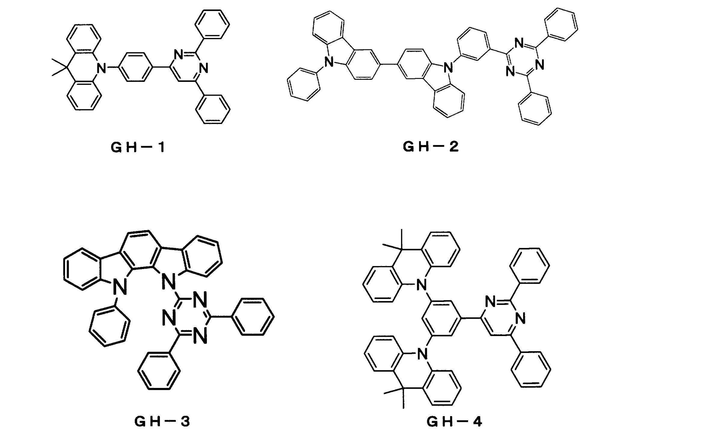
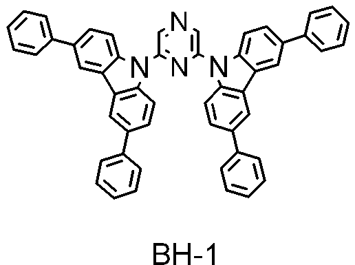
(基板)
本実施形態の有機EL素子は、透光性の基板上に作製する。この透光性基板は、有機EL素子を構成する陽極、有機化合物層、陰極等を支持する基板であり、400nm以上700nm以下の可視領域の光の透過率が50%以上で平滑な基板が好ましい。
透光性基板としては、ガラス板やポリマー板などが挙げられる。
ガラス板としては、特にソーダ石灰ガラス、バリウム・ストロンチウム含有ガラス、鉛ガラス、アルミノケイ酸ガラス、ホウケイ酸ガラス、バリウムホウケイ酸ガラス、石英などを原料として用いてなるものを挙げられる。
またポリマー板としては、ポリカーボネート、アクリル、ポリエチレンテレフタレート、ポリエーテルサルファイド、ポリサルフォンなどを原料として用いてなるものを挙げることができる。
(陽極および陰極)
有機EL素子の陽極は、正孔を発光層に注入する役割を担うものであり、4.5eV以上の仕事関数を有することが効果的である。
陽極材料の具体例としては、酸化インジウム錫合金(ITO)、酸化錫(NESA)、酸化インジウム亜鉛酸化物、金、銀、白金、銅などが挙げられる。
発光層からの発光を陽極側から取り出す場合、陽極の可視領域の光の透過率を10%より大きくすることが好ましい。また、陽極のシート抵抗は、数百Ω/□(Ω/sq。オーム・パー・スクウェア。)以下が好ましい。陽極の膜厚は、材料にもよるが、通常10nm以上1μm以下、好ましくは10nm以上200nm以下の範囲で選択される。
有機EL素子の陽極は、正孔を発光層に注入する役割を担うものであり、4.5eV以上の仕事関数を有することが効果的である。
陽極材料の具体例としては、酸化インジウム錫合金(ITO)、酸化錫(NESA)、酸化インジウム亜鉛酸化物、金、銀、白金、銅などが挙げられる。
発光層からの発光を陽極側から取り出す場合、陽極の可視領域の光の透過率を10%より大きくすることが好ましい。また、陽極のシート抵抗は、数百Ω/□(Ω/sq。オーム・パー・スクウェア。)以下が好ましい。陽極の膜厚は、材料にもよるが、通常10nm以上1μm以下、好ましくは10nm以上200nm以下の範囲で選択される。
陰極としては、発光層に電子を注入する目的で、仕事関数の小さい材料が好ましい。
陰極材料は特に限定されないが、具体的にはインジウム、アルミニウム、マグネシウム、マグネシウム-インジウム合金、マグネシウム-アルミニウム合金、アルミニウム-リチウム合金、アルミニウム-スカンジウム-リチウム合金、マグネシウム-銀合金などが使用できる。
陰極も、陽極と同様に、蒸着法などの方法で、例えば、電子輸送層や電子注入層上に薄膜を形成できる。また、陰極側から、発光層からの発光を取り出す態様を採用することもできる。発光層からの発光を陰極側から取り出す場合、陰極の可視領域の光の透過率を10%より大きくすることが好ましい。
陰極のシート抵抗は、数百Ω/□以下が好ましい。
陰極の膜厚は、材料にもよるが、通常10nm以上1μm以下、好ましくは50nm以上200nm以下の範囲で選択される。
(正孔注入・輸送層)
正孔注入・輸送層は、発光層への正孔注入を助け、発光領域まで輸送する層であって、正孔移動度が大きく、イオン化エネルギーが小さい化合物が用いられる。
正孔注入・輸送層を形成する材料としては、より低い電界強度で正孔を発光層に輸送する材料が好ましく、例えば、芳香族アミン化合物が好適に用いられる。
正孔注入・輸送層は、発光層への正孔注入を助け、発光領域まで輸送する層であって、正孔移動度が大きく、イオン化エネルギーが小さい化合物が用いられる。
正孔注入・輸送層を形成する材料としては、より低い電界強度で正孔を発光層に輸送する材料が好ましく、例えば、芳香族アミン化合物が好適に用いられる。
(電子注入・輸送層)
電子注入・輸送層は、発光層への電子の注入を助け、発光領域まで輸送する層であって、電子移動度が大きい化合物が用いられる。
電子注入・輸送層に用いられる化合物としては、例えば、分子内にヘテロ原子を1個以上含有する芳香族ヘテロ環化合物が好ましく用いられ、特に含窒素環誘導体が好ましい。含窒素環誘導体としては、含窒素6員環もしくは5員環骨格を有する複素環化合物が好ましい。
電子注入・輸送層は、発光層への電子の注入を助け、発光領域まで輸送する層であって、電子移動度が大きい化合物が用いられる。
電子注入・輸送層に用いられる化合物としては、例えば、分子内にヘテロ原子を1個以上含有する芳香族ヘテロ環化合物が好ましく用いられ、特に含窒素環誘導体が好ましい。含窒素環誘導体としては、含窒素6員環もしくは5員環骨格を有する複素環化合物が好ましい。
本発明の有機EL素子において、発光層以外の有機化合物層には、上述の例示した化合物以外に、従来の有機EL素子において使用される公知のものの中から任意の化合物を選択して用いることができる。
(層形成方法)
本発明の有機EL素子の各層の形成方法としては、上記で特に言及した以外には制限されないが、真空蒸着、スパッタリング、プラズマ、イオンプレーティングなどの乾式成膜法や、スピンコーティング、ディッピング、フローコーティング、インクジェットなどの湿式成膜法などの公知の方法を採用することができる。
本発明の有機EL素子の各層の形成方法としては、上記で特に言及した以外には制限されないが、真空蒸着、スパッタリング、プラズマ、イオンプレーティングなどの乾式成膜法や、スピンコーティング、ディッピング、フローコーティング、インクジェットなどの湿式成膜法などの公知の方法を採用することができる。
(膜厚)
本発明の有機EL素子の各有機層の膜厚は、上記で特に言及した以外には制限されないが、一般に膜厚が薄すぎるとピンホール等の欠陥が生じやすく、逆に厚すぎると高い印加電圧が必要となり効率が悪くなるため、通常は数nmから1μmの範囲が好ましい。
本発明の有機EL素子の各有機層の膜厚は、上記で特に言及した以外には制限されないが、一般に膜厚が薄すぎるとピンホール等の欠陥が生じやすく、逆に厚すぎると高い印加電圧が必要となり効率が悪くなるため、通常は数nmから1μmの範囲が好ましい。
(有機EL素子用材料)
本実施形態において、有機EL素子用材料は、上記一般式(1)で表される第一の材料と蛍光発光性ドーパント材料である第二の材料とを含むことが好ましい。
本実施形態において、有機EL素子用材料は、上記一般式(1)で表される第一の材料と蛍光発光性ドーパント材料である第二の材料とを含むことが好ましい。
[実施形態の変形]
なお、本発明は、上述の実施形態に限定されるものではなく、本発明の目的を達成できる範囲での変更、改良などは、本発明に含まれるものである。
なお、本発明は、上述の実施形態に限定されるものではなく、本発明の目的を達成できる範囲での変更、改良などは、本発明に含まれるものである。
発光層は、1層に限られず、複数の発光層が積層されていてもよい。有機EL素子が複数の発光層を有する場合、少なくとも1つの発光層が本発明で規定する上記ホスト材料と蛍光発光性ドーパント材料とを含んでいればよく、その他の発光層が蛍光発光型の発光層であっても、燐光発光型の発光層であってもよい。
また、有機EL素子が複数の発光層を有する場合、これらの発光層が互いに隣接して設けられていてもよい。
また、有機EL素子が複数の発光層を有する場合、これらの発光層が互いに隣接して設けられていてもよい。
上記実施形態では、発光層に蛍光発光性のドーパント材料を用いた例を挙げて説明したが、本発明の別の形態として、蛍光発光性のドーパント材料に限定されず重金属錯体ではないドーパント材料を用いる場合も含まれる。
その他、本発明の実施における具体的な構造および形状などは、本発明の目的を達成できる範囲で他の構造などとしてもよい。
以下、本発明に係る実施例を説明するが、本発明はこれらの実施例によって限定されない。
使用した化合物は、以下のとおりである。


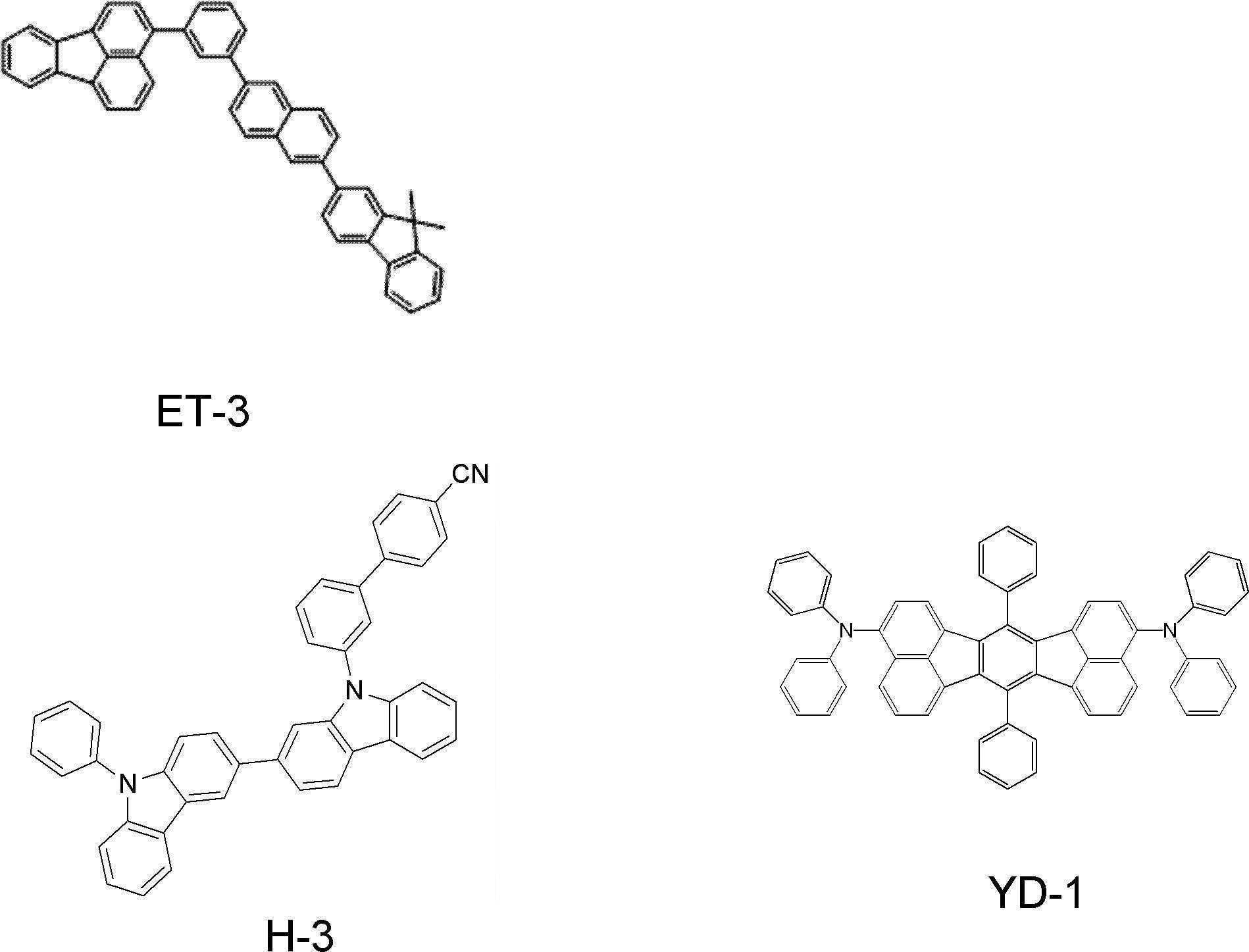
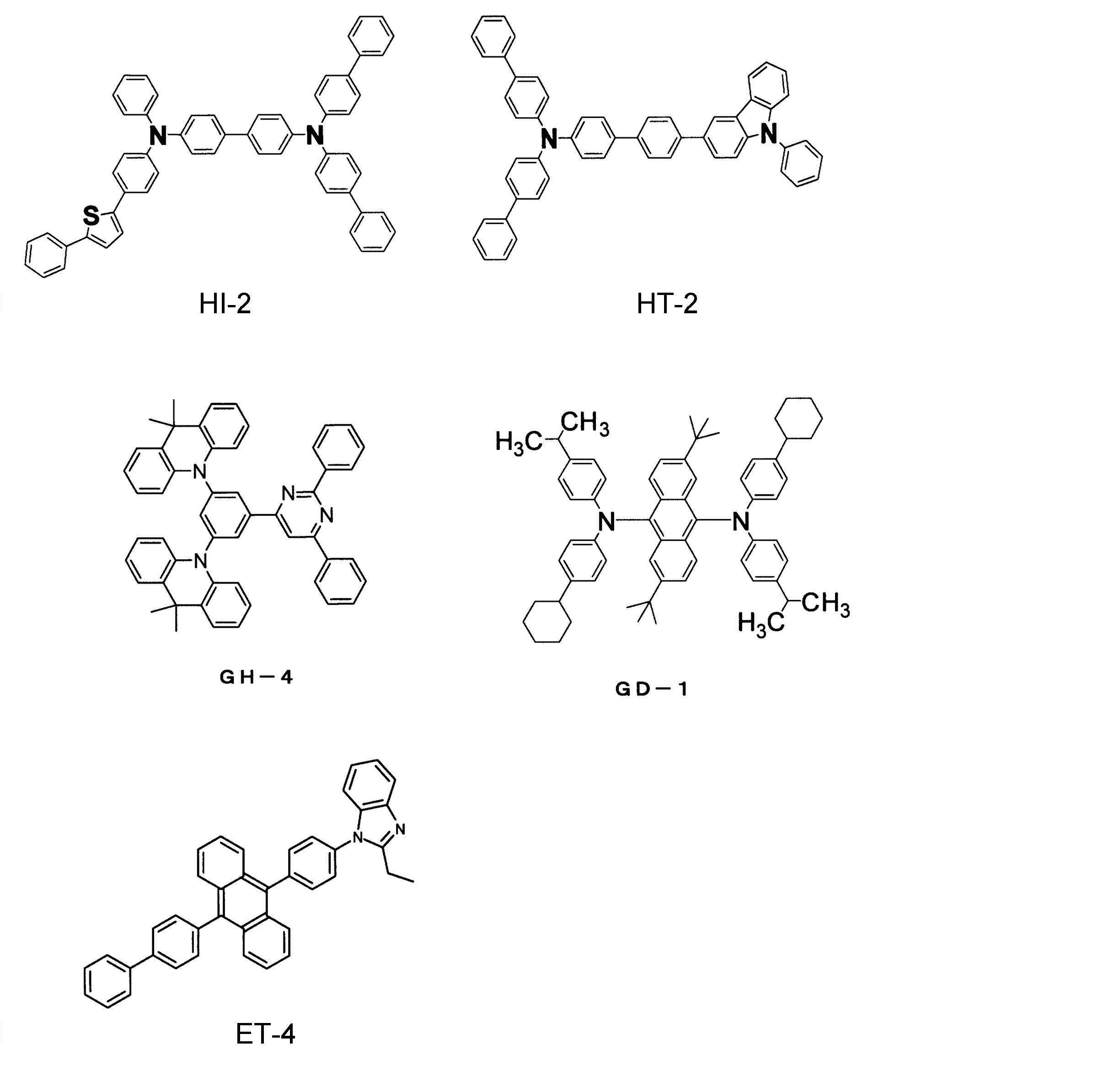

<化合物の合成>
〔合成例1〕 H-1の合成
・(1-1) 中間体1の合成
アルゴン気流下、2-ニトロ-1,4-ジブロモベンゼン(11.2g、40mmol)、フェニルボロン酸(4.9g、40mmol)、テトラキス(トリフェニルホスフィン)パラジウム(1.39g、1.2mmol)、トルエン(120mL)、2M炭酸ナトリウム水溶液(60mL)を順次加えて8時間加熱還流した。
室温まで反応液を冷却した後、有機層を分離し、有機溶媒を減圧下留去した。得られた残渣をシリカゲルカラムクロマトグラフィーにて精製し、中間体1(6.6g、収率59%)を得た。FD-MS(フィールドディソープションマススペクトル)の分析により、中間体1と同定した。

・(1-2) 中間体2の合成
アルゴン気流下、中間体1(6.6g、23.7mmol)、トリフェニルホスフィン(15.6g、59.3mmol)、o-ジクロロベンゼン(24mL)を順次加えて8時間180℃で加熱した。
室温まで反応液を冷却した後、シリカゲルカラムクロマトグラフィーにて精製し、中間体2(4g、収率68%)を得た。FD-MS(フィールドディソープションマススペクトル)の分析により、中間体2と同定した。
アルゴン気流下、中間体1(6.6g、23.7mmol)、トリフェニルホスフィン(15.6g、59.3mmol)、o-ジクロロベンゼン(24mL)を順次加えて8時間180℃で加熱した。
室温まで反応液を冷却した後、シリカゲルカラムクロマトグラフィーにて精製し、中間体2(4g、収率68%)を得た。FD-MS(フィールドディソープションマススペクトル)の分析により、中間体2と同定した。

・(1-3) 中間体3の合成
中間体1の合成において、2-ニトロ-1,4-ジブロモベンゼンの代わりに中間体2を用い、フェニルボロン酸の代わりに9-フェニル-9H-カルバゾール-3-イルボロン酸を用いて同様の方法で合成した。FD-MS(フィールドディソープションマススペクトル)の分析により、中間体3と同定した。
中間体1の合成において、2-ニトロ-1,4-ジブロモベンゼンの代わりに中間体2を用い、フェニルボロン酸の代わりに9-フェニル-9H-カルバゾール-3-イルボロン酸を用いて同様の方法で合成した。FD-MS(フィールドディソープションマススペクトル)の分析により、中間体3と同定した。
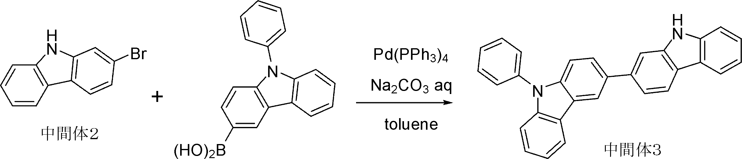
・(1-4) H-1の合成
アルゴン気流下、中間体3(3.3g、8.1mmol)、4-ブロモ-4’-シアノビフェニル(2.5g、9.7mmol)、トリス(ジベンジリデンアセトン)ジパラジウム(0.297、0.324mmol)、トリ-t-ブチルホスホニウムテトラフルオロほう酸塩(0.234g、0.805mmol)、t-ブトキシナトリウム(1.5g、16.2mmol)、無水キシレン(40mL)を順次加えて8時間加熱還流した。
室温まで反応液を冷却した後、有機層を分離し、有機溶媒を減圧下留去した。得られた残渣をシリカゲルカラムクロマトグラフィーにて精製し、2.6g(収率54%)の白色固体(H-1)を得た。
得られた化合物について、FD-MS(フィールドディソープションマススペクトル)、トルエン溶液中の紫外線吸収極大波長λmax、及び蛍光発光極大波長を以下に示す。
FDMS, calcd for C43H27N3=585, found m/z=585 (M+)
UV(PhMe);λmax, 324nm、FL(PhMe, λex=300nm);λmax, 393nm

〔合成例2〕 H-2の合成
・(2-1) 中間体4の合成
中間体1の合成において、2-ニトロ-1,4-ジブロモベンゼンの代わりに1-ブロ
モ-4-ヨードベンゼンを用い、フェニルボロン酸の代わりに9-フェニル-9H-カルバゾール-3-イルボロン酸を用いて同様の方法で合成した。FD-MS(フィールドディソープションマススペクトル)の分析により、中間体4と同定した。
・(2-1) 中間体4の合成
中間体1の合成において、2-ニトロ-1,4-ジブロモベンゼンの代わりに1-ブロ
モ-4-ヨードベンゼンを用い、フェニルボロン酸の代わりに9-フェニル-9H-カルバゾール-3-イルボロン酸を用いて同様の方法で合成した。FD-MS(フィールドディソープションマススペクトル)の分析により、中間体4と同定した。
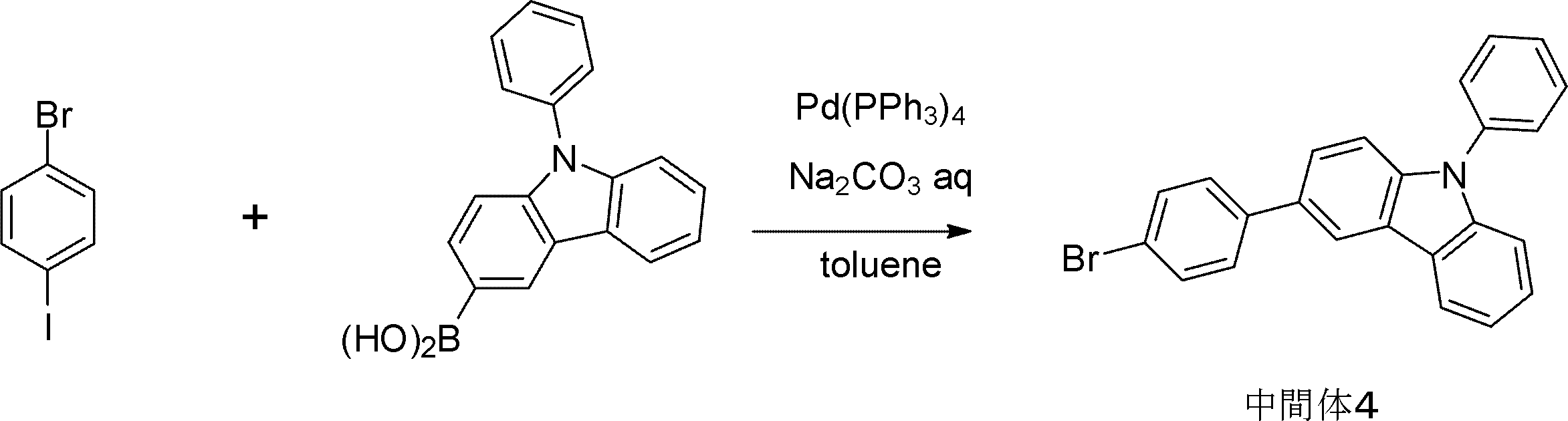
・(2-2) 中間体5の合成
アルゴン気流下、中間体4(10g、25mmol)、ビス(ピナコラト)ジボロン(8.3g、33mmol)、[1,1’-ビス(ジフェニルホスフィノ)フェロセン]パラジウム(II)ジクロリド ジクロロメタン付加物(0.62g、0.75mmol)、
酢酸カリウム(7.4g、75mmol)、N,N-ジメチルホルムアミド(170mL)を順次加えて8時間加熱還流した。
室温まで反応液を冷却した後、有機層を分離し、有機溶媒を減圧下留去した。得られた残渣をシリカゲルカラムクロマトグラフィーにて精製し、中間体5(10g、収率91%)を得た。FD-MS(フィールドディソープションマススペクトル)の分析により、中間体5と同定した。
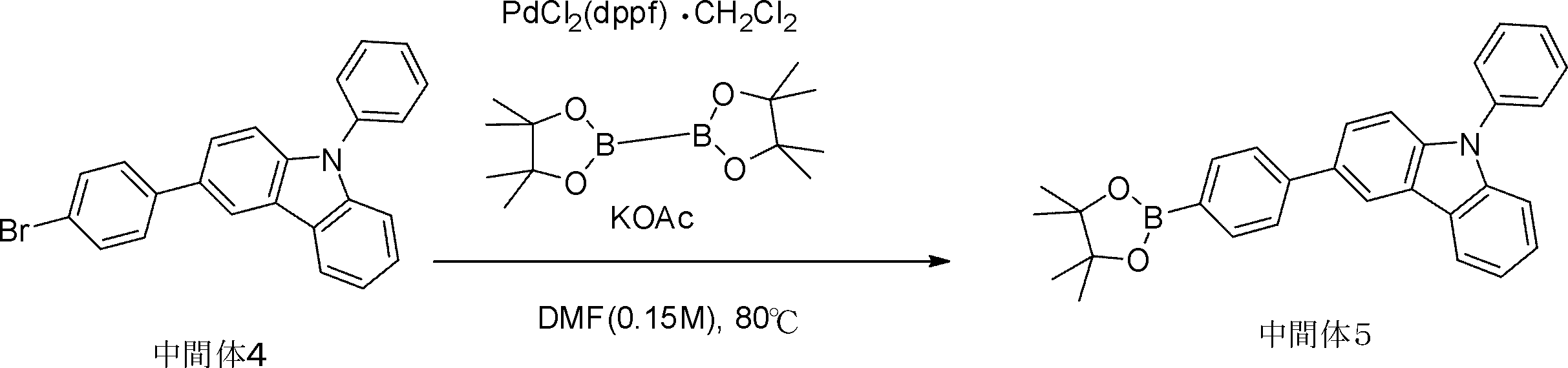
・(2-3) 中間体6の合成
中間体1の合成において、2-ニトロ-1,4-ジブロモベンゼンの代わりに3-ブロモカルバゾールを用い、フェニルボロン酸の代わりに中間体5を用いて同様の方法で合成した。FD-MS(フィールドディソープションマススペクトル)の分析により、中間体6と同定した。
中間体1の合成において、2-ニトロ-1,4-ジブロモベンゼンの代わりに3-ブロモカルバゾールを用い、フェニルボロン酸の代わりに中間体5を用いて同様の方法で合成した。FD-MS(フィールドディソープションマススペクトル)の分析により、中間体6と同定した。
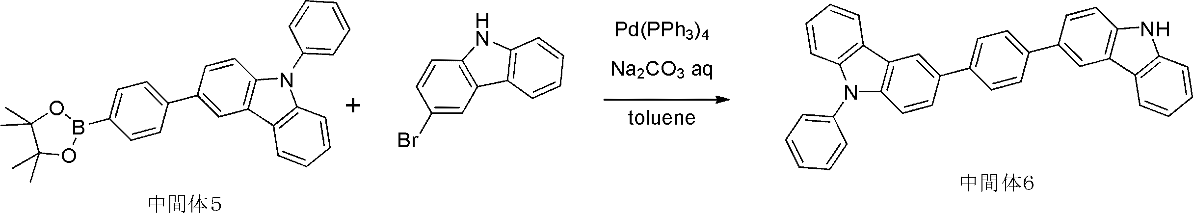
・(2-4) H-2の合成
H-1の合成において、4-ブロモ-4’-シアノビフェニルの代わりに3’-ブロモビフェニル-4-カルボニトリルを用い、中間体3の代わりに中間体6を用いて同様の方法で合成した。
得られた化合物について、FD-MS(フィールドディソープションマススペクトル)を以下に示す。
FDMS, calcd for C49H31N3=661, found m/z=661 (M+)
UV(PhMe);λmax, not detected、FL(PhMe, λex=300nm);λmax, 418nm
H-1の合成において、4-ブロモ-4’-シアノビフェニルの代わりに3’-ブロモビフェニル-4-カルボニトリルを用い、中間体3の代わりに中間体6を用いて同様の方法で合成した。
得られた化合物について、FD-MS(フィールドディソープションマススペクトル)を以下に示す。
FDMS, calcd for C49H31N3=661, found m/z=661 (M+)
UV(PhMe);λmax, not detected、FL(PhMe, λex=300nm);λmax, 418nm
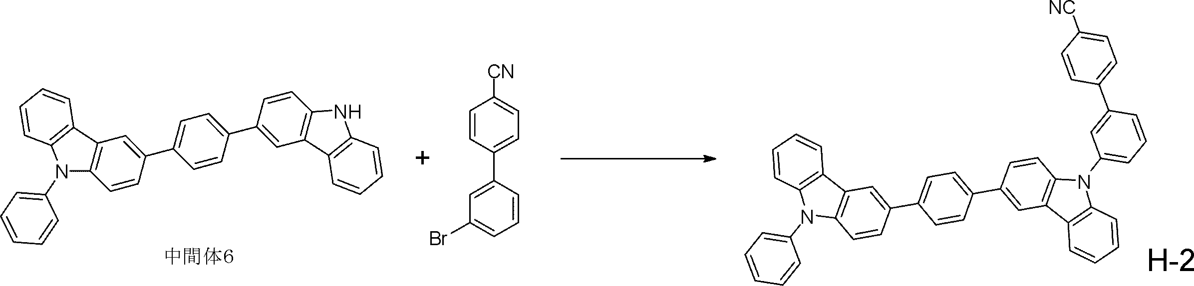
〔合成例3〕 H-3の合成
H-1の合成において、4-ブロモ-4’-シアノビフェニルの代わりに4’-ブロモビフェニル-3-カルボニトリルを用いて同様の方法で合成した。
得られた化合物について、FD-MS(フィールドディソープションマススペクトル)、トルエン溶液中の紫外線吸収極大波長λmax、及び蛍光発光極大波長を以下に示す。
FDMS, calcd for C43H27N3=585, found m/z=585 (M+)
UV(PhMe);λmax, 322nm、FL(PhMe, λex=300nm);λmax, 376nm
H-1の合成において、4-ブロモ-4’-シアノビフェニルの代わりに4’-ブロモビフェニル-3-カルボニトリルを用いて同様の方法で合成した。
得られた化合物について、FD-MS(フィールドディソープションマススペクトル)、トルエン溶液中の紫外線吸収極大波長λmax、及び蛍光発光極大波長を以下に示す。
FDMS, calcd for C43H27N3=585, found m/z=585 (M+)
UV(PhMe);λmax, 322nm、FL(PhMe, λex=300nm);λmax, 376nm

〔合成例4〕 GH-4の合成
アルゴン雰囲気下、特開2010180204号公報に記載の方法に従って合成した中間体A(4.4g、21mmol)、国際公開第2003/080760号に記載の方法に従って合成した中間体B(4.7g、10mmol)、トリス(ジベンジリデンアセトン)ジパラジウム(0.37g、0.4mmol)、トリ-t-ブチルホスホニウムテトラフルオロほう酸塩(0.46g、1.6mmol)、t-ブトキシナトリウム(2.7g、28mmol)、無水トルエン(100mL)を順次加えて8時間加熱還流した。
室温まで反応液を冷却した後、有機層を分離し、有機溶媒を減圧下で留去した。得られた残渣をシリカゲルカラムクロマトグラフィーにて精製し、目的化合物GH-4(3.6g、収率50%)を得た。
FD-MS分析の結果、分子量722に対してm/e=722であった。
以下に化合物GH-4の合成スキームを示す。
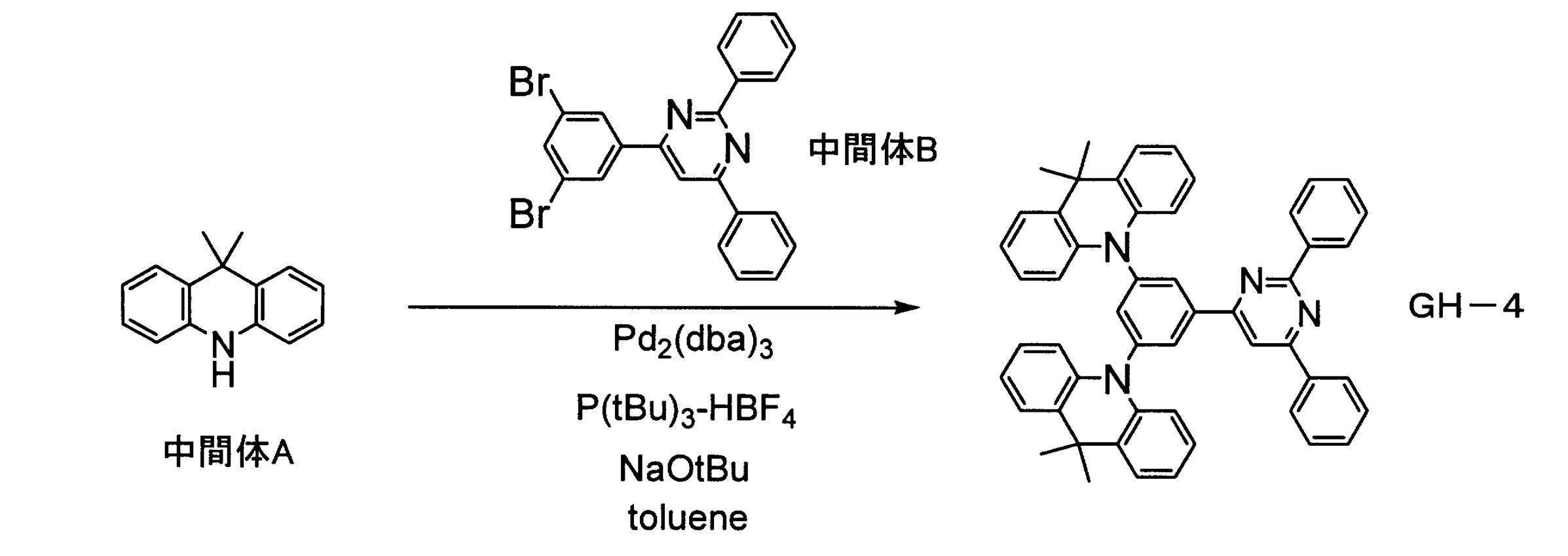
〔合成例5〕 BH-1の合成
・(5-1) 3,6-ジフェニルカルバゾールの合成
窒素雰囲気下、フラスコに3,6-ジブロモカルバゾール(5g、15.4mmol)、フェニルボロン酸(4.1g、33.9mmol)、テトラキス(トリフェニルホスフィン)パラジウム(0.7g, 0.6mmol)、トルエン(45ml)、2M炭酸ナトリウム(45ml)の順で加えて80℃で8時間攪拌した。有機相を分離した後にエバポレーターで減圧濃縮した。得られた残渣をシリカゲルカラムクロマトグラフィーで精製して3,6-ジフェニルカルバゾール(3.6g、収率74%)を得た。
窒素雰囲気下、フラスコに3,6-ジブロモカルバゾール(5g、15.4mmol)、フェニルボロン酸(4.1g、33.9mmol)、テトラキス(トリフェニルホスフィン)パラジウム(0.7g, 0.6mmol)、トルエン(45ml)、2M炭酸ナトリウム(45ml)の順で加えて80℃で8時間攪拌した。有機相を分離した後にエバポレーターで減圧濃縮した。得られた残渣をシリカゲルカラムクロマトグラフィーで精製して3,6-ジフェニルカルバゾール(3.6g、収率74%)を得た。
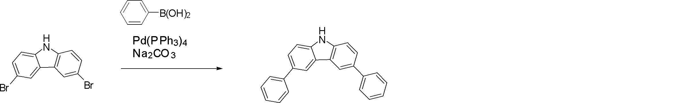
・(5-2) BH-1の合成
アルゴン雰囲気下、2,6-ジクロロピラジン(0.6g、3.9mmol)、3,6-ジブロモカルバゾール(2.6g、8mmol)、トリス(ジベンジリデンアセトン)ジパラジウム(0.07g、0.08mmol)、トリ-t-ブチルホスホニウムテトラフルオロほう酸塩(0.09g、0.3mmol)、t-ブトキシナトリウム(0.5g、5.5mmol)、および無水トルエン(20mL)を順次加えて、8時間加熱還流した。
室温まで反応液を冷却した後、有機層を分離し、有機溶媒を減圧下留去した。得られた残渣をシリカゲルカラムクロマトグラフィーにて精製し、1.8gの固体を得た。
得られた化合物について、FD-MSを行った結果、化合物BH-1と同定した。
FD-MS:
calcd for C52H34N4=714,found m/z=714(M+,100)
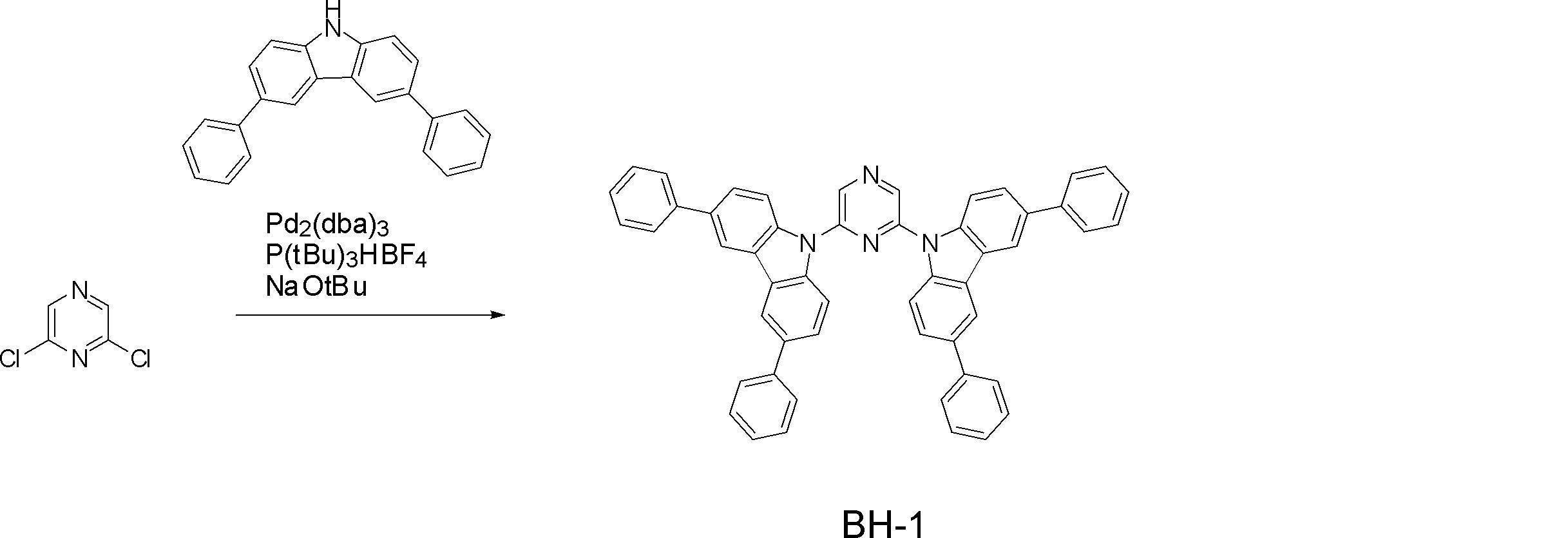
<化合物の評価>
次に、本実施例で使用した化合物の物性を測定した。対象化合物は、H-1~H-3、GH-4、GD-1、BH-1、およびBD-1である。測定方法、又は算出方法を以下に示すとともに、測定結果、又は算出結果を表1に示す。
次に、本実施例で使用した化合物の物性を測定した。対象化合物は、H-1~H-3、GH-4、GD-1、BH-1、およびBD-1である。測定方法、又は算出方法を以下に示すとともに、測定結果、又は算出結果を表1に示す。
(1-1)測定方法3の一重項エネルギーEgS
測定方法3の一重項エネルギーEgSは、以下の方法により求めた。
測定対象化合物を石英基板上に蒸着して試料を作製し、常温(300K)でこの試料の吸収スペクトルを測定した。試料の膜厚は100nmとした。吸収スペクトルは、縦軸を吸光度、横軸を波長とした。この吸収スペクトルの長波長側の立ち下がりに対して接線を引き、その接線と横軸との交点の波長値λedge[nm]を求めた。この波長値を次に示す換算式でエネルギー値に換算した値をEgSとした。
換算式:EgS[eV]=1239.85/λedge
吸収スペクトルの測定には、分光光度計(日立製、U3310)を用いた。
測定方法3の一重項エネルギーEgSは、以下の方法により求めた。
測定対象化合物を石英基板上に蒸着して試料を作製し、常温(300K)でこの試料の吸収スペクトルを測定した。試料の膜厚は100nmとした。吸収スペクトルは、縦軸を吸光度、横軸を波長とした。この吸収スペクトルの長波長側の立ち下がりに対して接線を引き、その接線と横軸との交点の波長値λedge[nm]を求めた。この波長値を次に示す換算式でエネルギー値に換算した値をEgSとした。
換算式:EgS[eV]=1239.85/λedge
吸収スペクトルの測定には、分光光度計(日立製、U3310)を用いた。
なお、吸収スペクトルの長波長側の立ち下がりに対する接線は以下のように引いた。吸収スペクトルの極大値のうち、最も長波長側の極大値から長波長方向にスペクトル曲線上を移動する際に、曲線上の各点における接線を考える。この接線は、曲線が立ち下がるにつれ(つまり縦軸の値が減少するにつれ)、傾きが減少しその後増加することを繰り返す。傾きの値が最も長波長側(ただし、吸光度が0.1以下となる場合は除く)で極小値をとる点において引いた接線を当該吸収スペクトルの長波長側の立ち下がりに対する接線とする。
なお、吸光度の値が0.2以下の極大点は、上記最も長波長側の極大値には含めなかった。
なお、吸光度の値が0.2以下の極大点は、上記最も長波長側の極大値には含めなかった。
(1-2)測定方法1のエネルギーギャップEg77K
測定方法1のEg77Kは、以下の方法により求めた。
各化合物を、公知の燐光測定法(例えば、「光化学の世界」(日本化学会編・1993)50頁付近の記載の方法)により測定した。具体的には、各化合物を溶媒に溶解(試料10[μmol/リットル]、EPA(ジエチルエーテル:イソペンタン:エタノール=5:5:5(容積比)、各溶媒は分光用グレード)し、燐光測定用試料とした。石英セルへ入れた燐光測定用試料を77[K]に冷却し、励起光を燐光測定用試料に照射し、波長を変えながら燐光強度を測定した。燐光スペクトルは、縦軸を燐光強度、横軸を波長とした。
この燐光スペクトルの短波長側の立ち上がりに対して接線を引き、その接線と横軸との交点の波長値λedge[nm]を求めた。この波長値を次に示す換算式でエネルギー値に換算した値をEg77Kとした。
換算式:Eg77K[eV]=1239.85/λedge
燐光スペクトルの短波長側の立ち上がりに対する接線は以下のように引いた。燐光スペクトルの短波長側から、スペクトルの極大値のうち、最も短波長側の極大値までスペクトル曲線上を移動する際に、長波長側に向けて曲線上の各点における接線を考える。この接線は、曲線が立ち上がるにつれ(つまり縦軸が増加するにつれ)、傾きが増加する。この傾きの値が極大値をとる点において引いた接線が、当該燐光スペクトルの短波長側の立ち上がりに対する接線とした。
なお、スペクトルの最大ピーク強度の10%以下のピーク強度をもつ極大点は、上述の最も短波長側の極大値には含めず、最も短波長側の極大値に最も近い、傾きの値が極大値をとる点において引いた接線を当該燐光スペクトルの短波長側の立ち上がりに対する接線とする。
燐光の測定には、(株)日立ハイテクノロジー製のF-4500形分光蛍光光度計本体と低温測定用オプション備品を用いた。なお、測定装置はこの限りではなく、冷却装置及び低温用容器と、励起光源と、受光装置とを組み合わせることにより、測定してもよい。
なお、スペクトルの最大ピーク強度の10%以下のピーク強度をもつ極大点は、上述の最も短波長側の極大値には含めず、最も短波長側の極大値に最も近い、傾きの値が極大値をとる点において引いた接線を当該燐光スペクトルの短波長側の立ち上がりに対する接線とする。
燐光の測定には、(株)日立ハイテクノロジー製のF-4500形分光蛍光光度計本体と低温測定用オプション備品を用いた。なお、測定装置はこの限りではなく、冷却装置及び低温用容器と、励起光源と、受光装置とを組み合わせることにより、測定してもよい。
(1-3)ΔST
ΔSTは、上記(1-1)で測定したEgSと、上記(1-2)で測定したEg77Kとの差として求めた(上記数式(2)参照)。結果を測定方法1のΔSTとして表1に示す。
ΔSTは、上記(1-1)で測定したEgSと、上記(1-2)で測定したEg77Kとの差として求めた(上記数式(2)参照)。結果を測定方法1のΔSTとして表1に示す。
(2-1)測定方法4の一重項エネルギーEgS
測定対象化合物を石英基板上に蒸着して試料を作製し、常温(300K)でこの試料の発光スペクトルを測定した。試料の膜厚は100nmとした。発光スペクトルは、励起光を発光測定用試料に照射し、波長を変えながら発光強度を測定した。発光スペクトルは、縦軸を発光強度とし、横軸を波長とした。この発光スペクトルの短波長側の立ち上がりに対して接線を引き、その接線と横軸との交点の波長値λedge[nm]を求めた。この波長値を次に示す換算式でエネルギー値に換算した値をEgSとした。
換算式:EgS[eV]=1239.85/λedge
発光スペクトルの測定には、分光光度計(日立製、U3310)を用いた。
測定対象化合物を石英基板上に蒸着して試料を作製し、常温(300K)でこの試料の発光スペクトルを測定した。試料の膜厚は100nmとした。発光スペクトルは、励起光を発光測定用試料に照射し、波長を変えながら発光強度を測定した。発光スペクトルは、縦軸を発光強度とし、横軸を波長とした。この発光スペクトルの短波長側の立ち上がりに対して接線を引き、その接線と横軸との交点の波長値λedge[nm]を求めた。この波長値を次に示す換算式でエネルギー値に換算した値をEgSとした。
換算式:EgS[eV]=1239.85/λedge
発光スペクトルの測定には、分光光度計(日立製、U3310)を用いた。
発光スペクトルの短波長側の立ち上がりに対する接線は以下のように引いた。発光スペクトルの短波長側から、スペクトルの極大値のうち、最も短波長側の極大値までスペクトル曲線上を移動する際に、長波長側に向けて曲線上の各点における接線を考える。この接線は、曲線が立ち上がるにつれ(つまり縦軸が増加するにつれ)、傾きが増加する。この傾きの値が極大値をとる点において引いた接線(すなわち変曲点における接線)が、当該発光スペクトルの短波長側の立ち上がりに対する接線とした。
なお、スペクトルの最大ピーク強度の15%以下のピーク強度をもつ極大点は、上述の最も短波長側の極大値には含めず、最も短波長側の極大値に最も近い、傾きの値が極大値をとる点において引いた接線を当該発光スペクトルの短波長側の立ち上がりに対する接線とする。
なお、スペクトルの最大ピーク強度の15%以下のピーク強度をもつ極大点は、上述の最も短波長側の極大値には含めず、最も短波長側の極大値に最も近い、傾きの値が極大値をとる点において引いた接線を当該発光スペクトルの短波長側の立ち上がりに対する接線とする。
(2-2)測定方法2のエネルギーギャップEg77K
測定対象化合物を石英基板上に蒸着して試料を作製し、膜厚は100nmとした。NMRチューブへ入れた燐光測定用試料を77[K]に冷却し、励起光を燐光測定用試料に照射し、波長を変えながら燐光強度を測定した。燐光スペクトルは、縦軸を燐光強度、横軸を波長とした。
この燐光スペクトルの短波長側の立ち上がりに対して接線を引き、その接線と横軸との交点の波長値λedge[nm]を求めた。この波長値を次に示す換算式でエネルギー値に換算した値をEg77Kとした。
換算式:Eg77K[eV]=1239.85/λedge
測定対象化合物を石英基板上に蒸着して試料を作製し、膜厚は100nmとした。NMRチューブへ入れた燐光測定用試料を77[K]に冷却し、励起光を燐光測定用試料に照射し、波長を変えながら燐光強度を測定した。燐光スペクトルは、縦軸を燐光強度、横軸を波長とした。
この燐光スペクトルの短波長側の立ち上がりに対して接線を引き、その接線と横軸との交点の波長値λedge[nm]を求めた。この波長値を次に示す換算式でエネルギー値に換算した値をEg77Kとした。
換算式:Eg77K[eV]=1239.85/λedge
燐光スペクトルの短波長側の立ち上がりに対する接線は以下のように引いた。燐光スペクトルの短波長側から、スペクトルの極大値のうち、最も短波長側の極大値までスペクトル曲線上を移動する際に、長波長側に向けて曲線上の各点における接線を考える。この接線は、曲線が立ち上がるにつれ(つまり縦軸が増加するにつれ)、傾きが増加する。この傾きの値が極大値をとる点において引いた接線(すなわち変曲点における接線)が、当該燐光スペクトルの短波長側の立ち上がりに対する接線とした。
なお、スペクトルの最大ピーク強度の15%以下のピーク強度をもつ極大点は、上述の最も短波長側の極大値には含めず、最も短波長側の極大値に最も近い、傾きの値が極大値をとる点において引いた接線を当該燐光スペクトルの短波長側の立ち上がりに対する接線とする。
燐光の測定には、(株)日立ハイテクノロジー製のF-4500形分光蛍光光度計本体を用いた。なお、測定装置はこの限りではなく、冷却装置及び低温用容器と、励起光源と、受光装置とを組み合わせることにより、測定してもよい。
なお、スペクトルの最大ピーク強度の15%以下のピーク強度をもつ極大点は、上述の最も短波長側の極大値には含めず、最も短波長側の極大値に最も近い、傾きの値が極大値をとる点において引いた接線を当該燐光スペクトルの短波長側の立ち上がりに対する接線とする。
燐光の測定には、(株)日立ハイテクノロジー製のF-4500形分光蛍光光度計本体を用いた。なお、測定装置はこの限りではなく、冷却装置及び低温用容器と、励起光源と、受光装置とを組み合わせることにより、測定してもよい。
(2-3)ΔST
ΔSTは、上記(2-1)で測定したEgSと、上記(2-2)で測定したEg77Kとの差として求めた(上記数式(数2)参照)。結果を測定方法2のΔSTとして表1に示す。
ΔSTは、上記(2-1)で測定したEgSと、上記(2-2)で測定したEg77Kとの差として求めた(上記数式(数2)参照)。結果を測定方法2のΔSTとして表1に示す。
また半値幅は、次のようにして求めた。
各化合物をガラス基板上に100nm、蒸着装置にて成膜し、蛍光測定用試料とした。
蛍光測定用試料に室温(300[K])で励起光を照射し、波長を変えながら蛍光強度を測定した。
フォトルミネッセンススペクトルは、縦軸を蛍光強度、横軸を波長とした。蛍光の測定に用いた装置は、(株)日立ハイテクノロジー製のF-4500形分光蛍光光度計である。
このフォトルミネッセンススペクトルから半値幅(単位は、nm。)を測定した。
半値幅を測定した化合物は、H-1、H-2、H-3である。結果を表1に示す。
各化合物をガラス基板上に100nm、蒸着装置にて成膜し、蛍光測定用試料とした。
蛍光測定用試料に室温(300[K])で励起光を照射し、波長を変えながら蛍光強度を測定した。
フォトルミネッセンススペクトルは、縦軸を蛍光強度、横軸を波長とした。蛍光の測定に用いた装置は、(株)日立ハイテクノロジー製のF-4500形分光蛍光光度計である。
このフォトルミネッセンススペクトルから半値幅(単位は、nm。)を測定した。
半値幅を測定した化合物は、H-1、H-2、H-3である。結果を表1に示す。

また、化合物H-1~H-3の分子軌道図をそれぞれ図9~11に示す。
<有機EL素子の作製、及び評価>
有機EL素子を以下のように作製し、評価した。
有機EL素子を以下のように作製し、評価した。
(実施例1)
25mm×75mm×1.1mm厚のITO透明電極(陽極)付きガラス基板(ジオマティック社製)をイソプロピルアルコール中で超音波洗浄を5分間行なった後、UVオゾン洗浄を30分間行なった。ITOの膜厚は、77nmとした。
洗浄後の透明電極ライン付きガラス基板を真空蒸着装置の基板ホルダーに装着し、まず透明電極ラインが形成されている側の面上に透明電極を覆うようにして化合物HI-1を蒸着し、膜厚5nmの化合物HI-1膜を形成した。このHI-1膜は、正孔注入層として機能する。
このHI-1膜の成膜に続けて、化合物HT-1を蒸着し、HI-1膜上に膜厚125nmのHT-1膜を成膜した。このHT-1膜は、第一の正孔輸送層として機能する。
このHT-1膜上に化合物HT-2を蒸着し膜厚25nmのHT-2膜を成膜した。このHT-2膜は第二の正孔輸送層として機能する。
さらにHT-2膜上に、化合物H-1(ホスト材料)および化合物BD-1(蛍光発光性ドーパント材料)を共蒸着し、膜厚25nmの発光層を成膜した。ドーパント材料濃度は、4質量%とした。
この発光層上に電子輸送性化合物であるET-1を蒸着し、膜厚5nmの正孔阻止層を形成した。
さらにET-1膜上に化合物ET-2とLiqを共蒸着し、膜厚20nmの電子輸送層を形成した。Liqの濃度は、50質量%とした。
この電子輸送層上にLiqを蒸着して、膜厚1nmのLiq層を形成した。
このLiq膜上に金属Alを蒸着して、膜厚80nmの金属陰極を形成した。
実施例1の有機EL素子の素子構成を略式的に示すと、次のとおりである。
ITO(77)/HI-1(5)/HT-1(125)/HT-2(25)/H-1:BD-1(25,4%)/ET-1(5)/ET-2:Liq(20,50%)/Liq(1)/Al(80)
なお、括弧内の数字は、膜厚(単位:nm)を示す。また、同じく括弧内において、パーセント表示された数字は、発光層における蛍光発光性ドーパント材料等のように、添加される成分の割合(質量%)を示す。
(実施例2)
25mm×75mm×1.1mm厚のITO透明電極(陽極)付きガラス基板(ジオマティック社製)をイソプロピルアルコール中で超音波洗浄を5分間行なった後、UVオゾン洗浄を30分間行なった。ITOの膜厚は、77nmとした。
洗浄後の透明電極ライン付きガラス基板を真空蒸着装置の基板ホルダーに装着し、まず透明電極ラインが形成されている側の面上に透明電極を覆うようにして化合物HI-1を蒸着し、膜厚5nmの化合物HI-1膜を形成した。このHI-1膜は、正孔注入層として機能する。
このHI-1膜の成膜に続けて、化合物HT-1を蒸着し、HI-1膜上に膜厚65nmのHT-1膜を成膜した。このHT-1膜の成膜に続けて、化合物HT-2を蒸着し、HT-1膜上に膜厚10nmのHT-2膜を成膜した。このHT-1、HT-2膜は、正孔輸送層として機能する。
このHT-2膜上に化合物H-2(ホスト材料)および化合物YD-1(蛍光発光性ドーパント材料)を共蒸着し、膜厚25nmの発光層を成膜した。ドーパント材料濃度は、4質量%とした。
この発光層上に電子輸送性化合物であるET-3を蒸着し、膜厚5nmの正孔阻止層を形成した。
この正孔阻止層上にET-2を蒸着して、膜厚30nmの電子輸送膜を形成した。
この電子輸送層上にLiFを蒸着し、膜厚1nmのLiF層を形成した。
このLiF膜上に金属Alを蒸着して、膜厚80nmの金属陰極を形成した。
実施例2の有機EL素子の素子構成を略式的に示すと、次のとおりである。
ITO(77)/HI-1(5)/HT-1(65)/HT-2(10)/H-2:YD-1(25,4%)/ET-3(5)/ET-2(30)/LiF(1)/Al(80)
なお、括弧内の数字は、膜厚(単位:nm)を示す。また、同じく括弧内において、パーセント表示された数字は、YD-1の割合(質量%)を示す。
(実施例3)
ホスト材料として、H-2の代わりにH-3を用いた以外は実施例2と同様にして有機EL素子を作製した。
(実施例4)
25mm×75mm×1.1mm厚のITO透明電極(陽極)付きガラス基板(ジオマティック社製)をイソプロピルアルコール中で超音波洗浄を5分間行なった後、UVオゾン洗浄を30分間行なった。ITOの膜厚は、130nmとした。
洗浄後の透明電極ライン付きガラス基板を真空蒸着装置の基板ホルダーに装着し、まず透明電極ラインが形成されている側の面上に透明電極を覆うようにして化合物HI-2を蒸着し、膜厚50nmの化合物HI-2膜を形成した。このHI-2膜は、正孔注入層として機能する。
このHI-2膜の成膜に続けて、化合物HT-2を蒸着し、HI-2膜上に膜厚60nmのHT-2膜を成膜した。このHT-2膜は、正孔輸送層として機能する。
このHT-2膜上に化合物GH-4(ホスト材料)および化合物GD-1(蛍光発光性ドーパント材料)を共蒸着し、膜厚30nmの発光層を成膜した。ドーパント材料濃度は、5質量%とした。
この発光層上に電子輸送性化合物であるET-4を蒸着し、膜厚25nmの電子輸送層を形成した。
この電子輸送層上にLiFを蒸着して、膜厚1nmのLiF膜を形成した。
このLiF膜上に金属Alを蒸着して、膜厚80nmの金属陰極を形成した。
このようにして、実施例4の有機EL素子を作製した。
実施例4の有機EL素子の素子構成を略式的に示すと、次のとおりである。
ITO(130)/HI-2(50)/HT-2(60)/GH-4:GD-1(30,5%)/ET-4(25)/LiF(1)/Al(80)
(実施例5)
25mm×75mm×1.1mm厚のITO透明電極(陽極)付きガラス基板(ジオマティック社製)をイソプロピルアルコール中で超音波洗浄を5分間行なった後、UVオゾン洗浄を30分間行なった。ITOの膜厚は、70nmとした。
洗浄後の透明電極ライン付きガラス基板を真空蒸着装置の基板ホルダーに装着し、まず透明電極ラインが形成されている側の面上に透明電極を覆うようにして化合物HI-1を蒸着し、膜厚5nmの化合物HI-1膜を形成した。このHI-1膜は、正孔注入層として機能する。
このHI-1膜の成膜に続けて、化合物HT-1を蒸着し、HI-1膜上に膜厚125nmのHT-1膜を成膜した。このHT-1膜の成膜に続けて、化合物HT-2を蒸着し、HT-1膜上に膜厚25nmのHT-2膜を成膜した。このHT-1、HT-2膜は、正孔輸送層として機能する。
このHT-2膜上に化合物BH-1(ホスト材料)および化合物BD-1(蛍光発光性ドーパント材料)を共蒸着し、膜厚25nmの発光層を成膜した。ドーパント材料濃度は、4質量%とした。
この発光層上に電子輸送性化合物であるET-1を蒸着し、膜厚5nmの正孔阻止層を形成した。
この正孔阻止層上にET-2およびLiqを共蒸着して、膜厚20nmの電子輸送膜を形成した。ET-2およびLiqの濃度比は50質量%:50質量%とした。
この電子輸送層上にLiqを蒸着し、膜厚1nmのLiq層を形成した。
このLiq膜上に金属Alを蒸着して、膜厚80nmの金属陰極を形成した。
このようにして、実施例5の有機EL素子を作製した。
実施例5の有機EL素子の素子構成を略式的に示すと、次のとおりである。
ITO(70)/HI-1(5)/HT-1(125)/HT-2(25)/BH-1:BD-1(25,4%)/ET-1(5)/ET-2:Liq(20,50%)/Liq(1)/Al(80)
〔有機EL素子の評価〕
作製した有機EL素子について、駆動電圧、輝度、CIE1931色度、電流効率L/J、電力効率η、主ピーク波長λp、外部量子効率EQEの評価を行った。電流密度は、1.00mA/cm2または10.00mA/cm2とした。結果を表2に示す。
また、作製した有機EL素子について、電流密度は、1.00mA/cm2として、遅延蛍光比率および残存強度比の評価を行った。詳細を以下に示す。
作製した有機EL素子について、駆動電圧、輝度、CIE1931色度、電流効率L/J、電力効率η、主ピーク波長λp、外部量子効率EQEの評価を行った。電流密度は、1.00mA/cm2または10.00mA/cm2とした。結果を表2に示す。
また、作製した有機EL素子について、電流密度は、1.00mA/cm2として、遅延蛍光比率および残存強度比の評価を行った。詳細を以下に示す。
・駆動電圧
電流密度が1.00mA/cm2または10.00mA/cm2となるようにITOとAlとの間に通電したときの電圧(単位:V)を計測した。
電流密度が1.00mA/cm2または10.00mA/cm2となるようにITOとAlとの間に通電したときの電圧(単位:V)を計測した。
・CIE1931色度
電流密度が1.00mA/cm2または10.00mA/cm2となるように素子に電圧を印加した時のCIE1931色度座標(x、y)を分光放射輝度計CS-1000(コニカミノルタ社製)で計測した。
電流密度が1.00mA/cm2または10.00mA/cm2となるように素子に電圧を印加した時のCIE1931色度座標(x、y)を分光放射輝度計CS-1000(コニカミノルタ社製)で計測した。
・電流効率L/J、及び電力効率η
電流密度が1.00mA/cm2または10.00mA/cm2となるように素子に電圧を印加した時の分光放射輝度スペクトルを上記分光放射輝度計で計測し、得られた分光放射輝度スペクトルから、電流効率(単位:cd/A)、及び電力効率η(単位:lm/W)を算出した。
電流密度が1.00mA/cm2または10.00mA/cm2となるように素子に電圧を印加した時の分光放射輝度スペクトルを上記分光放射輝度計で計測し、得られた分光放射輝度スペクトルから、電流効率(単位:cd/A)、及び電力効率η(単位:lm/W)を算出した。
・主ピーク波長λp
得られた上記分光放射輝度スペクトルから主ピーク波長λpを求めた。
得られた上記分光放射輝度スペクトルから主ピーク波長λpを求めた。
・外部量子効率EQE
得られた上記分光放射輝度スペクトルから、ランバシアン放射を行なったと仮定し外部量子効率EQE(単位:%)を算出した。
得られた上記分光放射輝度スペクトルから、ランバシアン放射を行なったと仮定し外部量子効率EQE(単位:%)を算出した。
・遅延蛍光比率
パルスジェネレータ(アジレント社製8114A)から出力した電圧パルス波形(パルス幅:500マイクロ秒、周波数:20Hz、電圧:0.1~100mA/cm2相当の電圧)を印加し、EL発光を光電子増倍管(浜松ホトニクス社製R928)に入力し、パルス電圧波形とEL発光とを同期させてオシロスコープ(テクトロニクス社製2440)に取り込んで過渡EL波形を得た。光強度の平方根の逆数をプロットし、これを最小二乗法により10-5秒までの値を用いて直線へフィッティングし、遅延蛍光比率を決定した。
実施例1の有機EL素子に対して、室温下、1.00mA/cm2で通電した時の過渡EL波形を、図12に示した。時刻約3×10-8秒のところでパルス電圧を除去した。
電圧除去時点を原点にとり、電圧除去後、1.5×10⁻⁵秒までの光強度の平方根の逆数をプロットし、このグラフから求めた実施例1の有機EL素子における遅延蛍光比率は45.9%であった。この遅延蛍光比率の値は、TTF比率の理論値限界37.5%を超えるものであった。
また、図12から、1μsにおける残存強度比を読み取ったところ、46.2%であった。
実施例2~5の有機EL素子についても、実施例1と同様の方法で、過渡EL波形を得た。光強度の平方根の逆数をプロットし、これを最小二乗法により10-5秒までの値を用いて直線へフィッティングし、解析して遅延蛍光比率を決定し、1μsにおける残存強度比を求めた。実施例2~3および実施例5の有機EL素子の過渡EL波形を、それぞれ図13~15に示す。なお、実施例4の有機EL素子の過渡EL波形は、前述の図6Aである。
また、実施例1~5の有機EL素子の遅延蛍光比率および残存強度比を表3に示す。
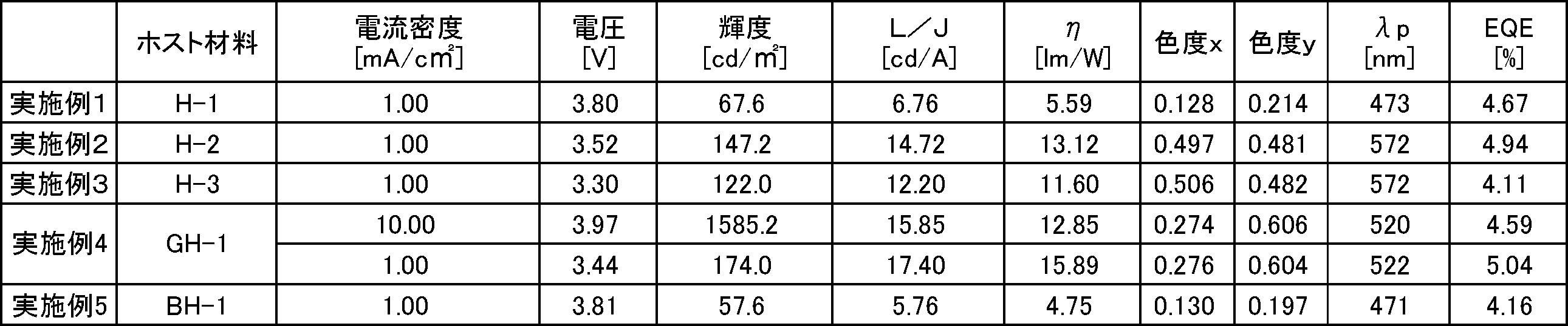

(参考例)
ここで、非特許文献1に記載された有機EL素子を参考例として挙げ、実施例1の有機EL素子の素子構成との比較を行う。
この参考例の有機EL素子の構成は、実施例1の略式的表示に倣って示すと、次のとおりである。
ITO(110)/NPD(40)/m-CP(10)/m-CP:PIC-TRZ(20,6%)/BP4mPy(40)/LiF(0.8)/Al(70)
参考例の素子に使用された化合物を以下に示す。
ここで、非特許文献1に記載された有機EL素子を参考例として挙げ、実施例1の有機EL素子の素子構成との比較を行う。
この参考例の有機EL素子の構成は、実施例1の略式的表示に倣って示すと、次のとおりである。
ITO(110)/NPD(40)/m-CP(10)/m-CP:PIC-TRZ(20,6%)/BP4mPy(40)/LiF(0.8)/Al(70)
参考例の素子に使用された化合物を以下に示す。
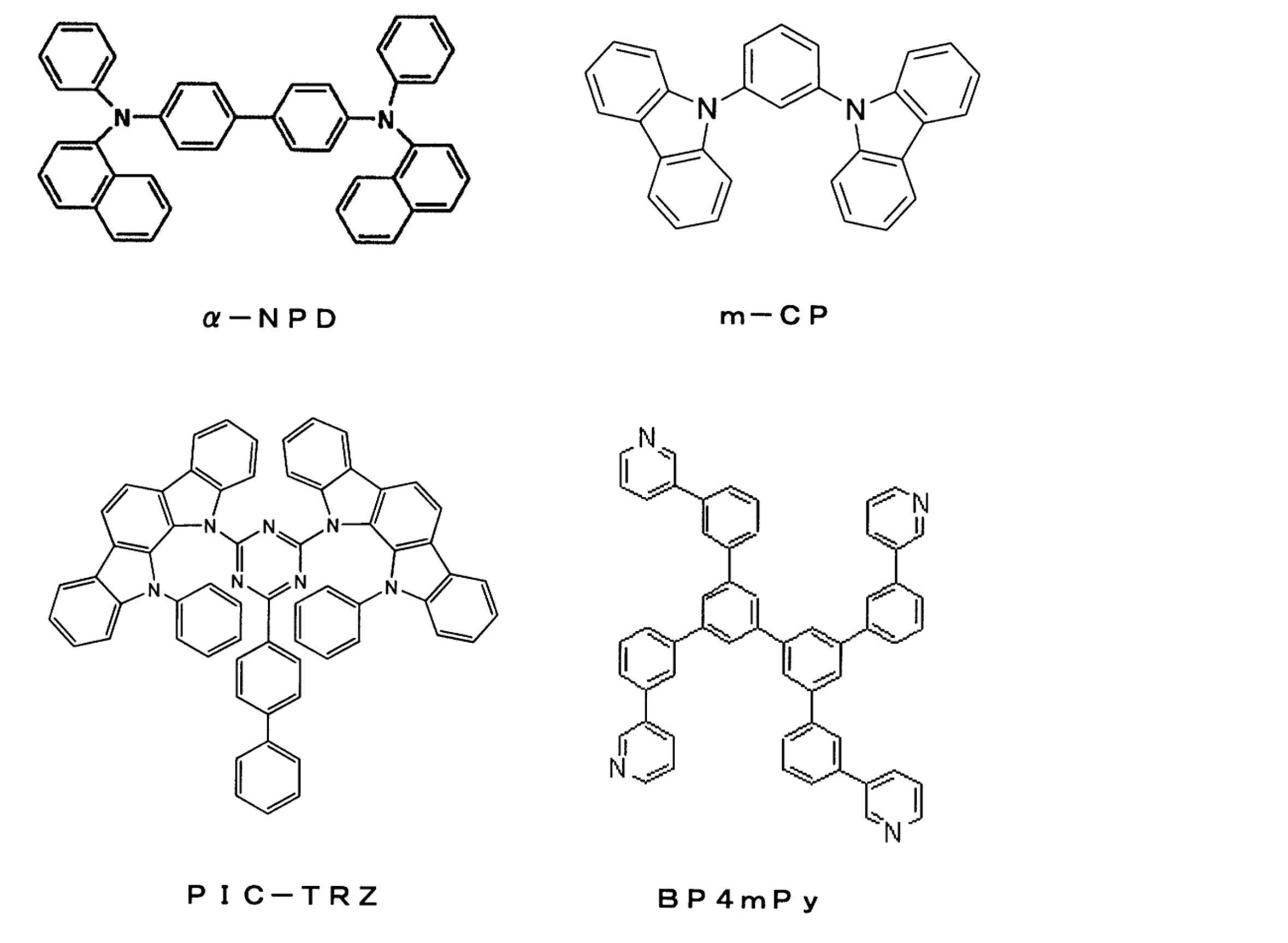
この素子の、EQEは、実使用領域よりも相当低い電流密度領域である0.01mA/cm2で、最大の5.1%を示すにとどまる。そのため、1mA/cm2程度の高電流密度領域では、ロールオフが生じ、発光効率が低下してしまうという問題がある。
したがって、実施例1~5の有機EL素子は、高電流密度領域でも高効率で発光したことが分かる。
本発明は、実用的な高電流密度領域でも効率的に発光する有機EL素子を提供できる。
1…有機EL素子
2…基板
3…陽極
4…陰極
5…発光層
6…正孔注入層
7…正孔輸送層
8…電子輸送層
9…電子注入層
10…有機化合物層
2…基板
3…陽極
4…陰極
5…発光層
6…正孔注入層
7…正孔輸送層
8…電子輸送層
9…電子注入層
10…有機化合物層
Claims (11)
- 陰極と、
陽極と、
前記陰極と前記陽極との間に配置された、少なくとも発光層を含む1層以上の有機薄膜層と、
を有し、
前記発光層が、下記一般式(1)で表される第一の材料と蛍光発光性ドーパント材料である第二の材料とを含む
ことを特徴とする有機エレクトロルミネッセンス素子。

(前記一般式(1)において、
Aは下記一般式(a-1)~(a-7)から選ばれる部分構造を有する基であり、
Bは下記一般式(b-1)~(b-6)から選ばれる部分構造を有する基であり、
Lは、単結合または連結基である。
連結基は、
置換もしくは無置換の環形成炭素数6~30のアリール基、
置換もしくは無置換の環形成原子数5~30の複素環基、または
これらの基が互いに2~5個連結した基のいずれかから誘導される基である。
なお、互いに連結した基は、互いに同一または異なる。
aは、Lに直接結合するAの置換数を表す1~5の整数であり、
aが2以上の場合、複数のAは互いに同じまたは異なる。
bは、Lに直接結合するBの置換数を表す1~5の整数であり、
bが2以上の場合、複数のBは互いに同じまたは異なる。)

(前記一般式(b-1)~(b-6)において、
Rは、
水素原子、
置換もしくは無置換の環形成炭素数6~30のアリール基、
置換もしくは無置換の環形成原子数5~30の複素環基、または
置換もしくは無置換の炭素数1~30のアルキル基、である。
複数のRが存在する場合は互いに同じまたは異なる。複数のRは互いに結合して環を形成する場合と、しない場合とがある。) - 請求項1に記載の有機エレクトロルミネッセンス素子において、
前記一般式(1)におけるBが下記一般式(2),(3),(4),(5)および(6)のいずれかで表される
ことを特徴とする有機エレクトロルミネッセンス素子。
R1~R8は、それぞれ独立して、
水素原子、
置換もしくは無置換の環形成炭素数6~30のアリール基、
置換もしくは無置換の環形成原子数5~30の複素環基
置換もしくは無置換の炭素数1~30のアルキル基、
置換もしくは無置換の炭素数3~30のアルキルシリル基、
置換もしくは無置換の環形成炭素数6~60のアリールシリル基、
置換もしくは無置換の炭素数1~30のアルコキシ基、
置換もしくは無置換の環形成炭素数6~30のアリールオキシ基、
置換もしくは無置換の炭素数2~30のアルキルアミノ基、
置換もしくは無置換の環形成炭素数6~60のアリールアミノ基、
置換もしくは無置換の炭素数1~30のアルキルチオ基、または、
置換もしくは無置換の環形成炭素数6~30のアリールチオ基である。
ただし、R1とR2、R2とR3、R3とR4、R5とR6、R6とR7、およびR7とR8のいずれかの組み合わせが飽和または不飽和の環構造を形成していてもよい。
L1は、下記一般式(21)~(27)から選ばれる連結基のいずれかを表す。
n1は1~3の整数を表し、n1が2または3の場合、複数のL1は互いに同じまたは異なる。
X1は、下記一般式(41)~(45)から選ばれる連結基のいずれかを表す。)

(前記一般式(23)~(27)において、R101は、前記一般式(2)におけるR1~R8と同義である。
ただし、前記一般式(2)において、R1~R8のうち一つまたはR101のうち一つは、Lに対して結合する単結合である。
複数のR101が存在する場合は、互いに同じまたは異なる。)

(前記一般式(43)~(45)において、Rxは、
水素原子、
置換もしくは無置換の環形成炭素数6~30のアリール基、
置換もしくは無置換の環形成原子数5~30の複素環基、または
置換もしくは無置換の炭素数1~30のアルキル基である。
複数のRxが存在する場合は互いに同じまたは異なる。)
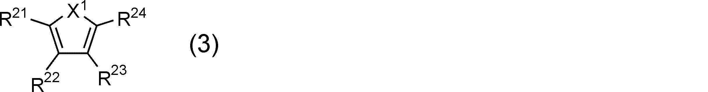
(前記一般式(3)において、R21~R24は、前記一般式(2)におけるR1~R8と同義である。
ただし、R21とR22、R22とR23、およびR23とR24のいずれかの組み合わせが飽和または不飽和の環構造を形成していてもよい。
X1は前記式(41)~(45)から選ばれる連結基のいずれかを表す。
ただし、前記一般式(3)において、R21~R24およびRxのうち一つは、Lに対して結合する単結合である。)

(前記一般式(4)において、
R25~R30は、前記一般式(2)におけるR1~R8と同義である。
ただし、R25とR26、R27とR28、R28とR29、およびR29とR30のいずれかの組み合わせが飽和または不飽和の環構造を形成していてもよい。
X1は前記式(41)~(45)から選ばれる連結基のいずれかを表す。
ただし、前記一般式(4)において、R25~R30およびRxのうちの一つは、Lに対して結合する単結合である。)

(前記一般式(5)において、
R31~R38は、前記一般式(2)におけるR1~R8と同義である。
ただし、R31とR32、R32とR33、R33とR34、R35とR36、R36とR37、R37とR38のいずれかの組み合わせが飽和または不飽和の環構造を形成していてもよい。
X1は前記一般式(41)~(45)から選ばれる連結基のいずれかを表す。
ただし、前記一般式(5)において、R31~R38およびRxのうちの一つは、Lに対して結合する単結合である。)

(前記一般式(6)において、
Arbは置換または無置換の環形成炭素数6~30のアリール基である。
Zbは、
置換もしくは無置換の炭素数4~30の三級アルキル基、
置換もしくは無置換の炭素数3~30のアルキルシリル基、
置換もしくは無置換の環形成炭素数6~60のアリールシリル基、
置換もしくは無置換の炭素数1~30のアルコキシ基、
置換もしくは無置換の環形成炭素数6~30のアリールオキシ基、
置換もしくは無置換の炭素数2~60のアルキルアミノ基、
置換もしくは無置換の環形成炭素数6~60のアリールアミノ基、
置換もしくは無置換の炭素数1~30のアルキルチオ基、または
置換もしくは無置換の環形成炭素数6~30のアリールチオ基である。
rは、Arbに直接結合するZbの置換数を表す1~5の整数であり、
rが2以上の場合、複数のZbはそれぞれ同じまたは異なる。) - 請求項2に記載の有機エレクトロルミネッセンス素子において、
前記一般式(2)は、下記一般式(2a)で表される
ことを特徴とする有機エレクトロルミネッセンス素子。

(前記一般式(2a)において、R10は、前記一般式(2)におけるR1~R8と同義である。
m1およびm3は0から4までの整数、m2は0から2までの整数を表す。
複数のR10は、互いに同じまたは異なる。
X1は前記式(41)~(45)から選ばれる連結基のいずれかを表す。
複数のX1は、互いに同じ、または異なる。
ただし、前記一般式(2a)において、R10および前記式(43)~(45)のRxのうち一つは、Lに対して結合する単結合である。) - 請求項2に記載の有機エレクトロルミネッセンス素子において、
前記一般式(5)におけるR31~R38の少なくともいずれか1つは、下記一般式(51)で表される
ことを特徴とする有機エレクトロルミネッセンス素子。

(前記一般式(51)において、
R39は、前記一般式(2)におけるR1~R8と同義である。
rは0から3までの整数を表し、Sは0から4までの整数を表す。
複数のR39は、互いに同一または異なる。
X1は前記一般式(41)~(45)から選ばれる連結基のいずれかを表す。
L61は単結合または連結基である。
連結基は、
置換もしくは無置換の環形成炭素数6~30のアリール基、
置換もしくは無置換の環形成原子数5~30の複素環基、または
これらの基が互いに2~5個連結した基のいずれかから誘導される基である。
なお、互いに連結した基は、互いに同一または異なる。) - 請求項1から請求項4までのいずれか一項に記載の有機エレクトロルミネッセンス素子において、
前記一般式(1)におけるAが、下記一般式(8),(9),(10),(11),(12),(13)および(14)のいずれかで表される
ことを特徴とする有機エレクトロルミネッセンス素子。
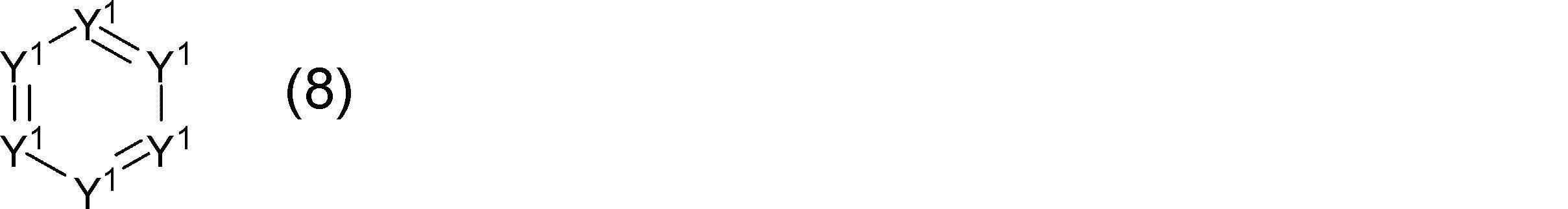
(前記一般式(8)において、Y1のうち2~4個は窒素原子であり、1つは、Lに結合する炭素原子であり、その他のY1は、CRyである。
前記一般式(8)が複数のRyを有する場合、Ryは、それぞれ独立して、
水素原子、
フッ素原子、
シアノ基、
ニトロ基、
置換もしくは無置換の環形成炭素数6~30のアリール基、
置換もしくは無置換の環形成原子数5~30の複素環基、
置換もしくは無置換の炭素数1~30のアルキル基、
置換もしくは無置換の炭素数1~30のアルキルカルボニル基、
置換もしくは無置換の環形成炭素数6~30のアリールカルボニル基、
置換もしくは無置換の炭素数1~30のアルキルスルフィニル基、
置換もしくは無置換の環形成炭素数6~30のアリールスルフィニル基、
置換もしくは無置換の炭素数2~60のアルキルホスフィニル基、
置換もしくは無置換の環形成炭素数6~60のアリールホスフィニル基、
置換もしくは無置換の炭素数1~30のアルキルスルホニル基、
置換もしくは無置換の環形成炭素数6~30のアリールスルホニル基、
置換もしくは無置換の炭素数3~60のアルキルシリル基、
置換もしくは無置換の環形成炭素数8~60のアリールシリル基、
置換もしくは無置換の炭素数1~30のアルコキシ基、または、
置換もしくは無置換の環形成炭素数6~30のアリールオキシ基である。
隣接する2つのY1がCRyであるとき、隣接する2つのY1が飽和または不飽和の環構造を形成していてもよい。)
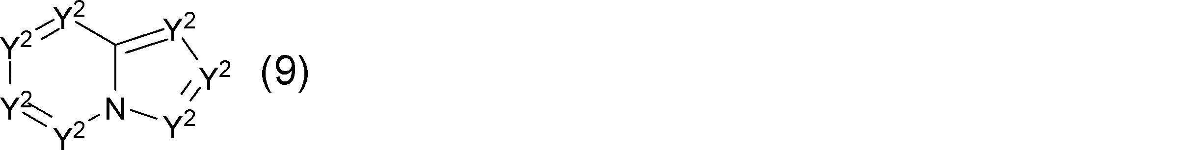
(前記一般式(9)において、Y2は前記一般式(8)におけるY1と同義である。)

(前記一般式(10),(11),(12)において、
Y3は前記一般式(8)におけるY1と同義である。
X3は下記一般式(41)~(45)から選ばれる連結基のいずれかを表す。)

(前記一般式(43)~(45)において、
Rxは、それぞれ独立に、
水素原子、
置換もしくは無置換の炭素数6~30のアリール基、
置換もしくは無置換の環形成原子数5~30の複素環基、または
置換もしくは無置換の炭素数1~30のアルキル基である。
複数のRxが存在する場合は互いに同じまたは異なる。)

(前記一般式(13)において、
R41~R48のうち一つはLに対して結合する単結合であり、
その他のR41~R48は、前記一般式(8)におけるRyと同義である。
L4は下記一般式(131)~(136)から選ばれる連結基のいずれかを表す。
pは1~3の整数を表し、pが2または3の場合、複数のL4は互いに同じまたは異なる。)

(前記一般式(133)~(136)において、
R301は、それぞれ独立に、
水素原子、
置換もしくは無置換の環形成炭素数6~30のアリール基、
置換もしくは無置換の環形成原子数5~30の複素環基、または
置換もしくは無置換の炭素数1~30のアルキル基である。
複数のR301が存在する場合は互いに同じまたは異なる。)

(前記一般式(14)において、
Araは、
置換もしくは無置換の環形成炭素数6~30のアリール基、または、
置換もしくは無置換の環形成原子数5~30の複素環基である。
Zaは、
フッ素原子、
シアノ基、
ニトロ基、
置換もしくは無置換の炭素数1~20のアルキルカルボニル基、
置換もしくは無置換の環形成炭素数6~30のアリールカルボニル基、
置換もしくは無置換の炭素数1~20のアルキルスルフィニル基、
置換もしくは無置換の環形成炭素数6~30のアリールスルフィニル基、
置換もしくは無置換の炭素数2~60のアルキルホスフィニル基、
置換もしくは無置換の環形成炭素数6~60のアリールホスフィニル基、
置換もしくは無置換の炭素数1~30のアルキルスルホニル基、または、
置換もしくは無置換の環形成炭素数6~30のアリールスルホニル基である。
qは、Araに直接結合するZaの置換数を表す1~5の整数であり、
qが2以上の場合、複数のZaは、互いに同一または異なる。) - 請求項1から請求項5までのいずれか一項に記載の有機エレクトロルミネッセンス素子において、
前記蛍光発光性ドーパント材料である第二の材料は、下記一般式(20)で表される
ことを特徴とする有機エレクトロルミネッセンス素子。
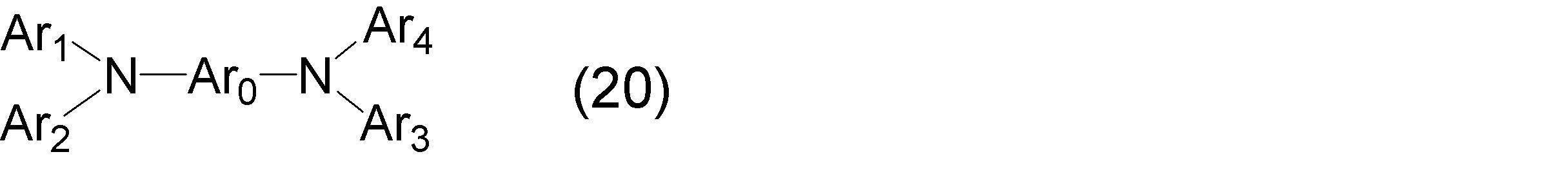
(前記一般式(20)において、
Ar0は、置換もしくは無置換の環形成炭素数10~50の2価の縮合芳香族炭化水素基であり、
Ar1~Ar4は、それぞれ独立に、
置換もしくは無置換の環形成炭素数6~30のアリール基、
置換もしくは無置換の環形成原子数5~30の複素環基、
置換もしくは無置換の炭素数6~30のアルキル基、または、
置換もしくは無置換の炭素数7~30のアラルキル基である。) - 請求項1から請求項6までのいずれか一項に記載の有機エレクトロルミネッセンス素子において、
遅延蛍光比率が37.5%より大きい
ことを特徴とする有機エレクトロルミネッセンス素子。 - 請求項1から請求項7までのいずれか一項に記載の有機エレクトロルミネッセンス素子において、
過渡EL測定における電圧除去後1μs経過後の残存強度比が36.0%より大きい
ことを特徴とする有機エレクトロルミネッセンス素子。 - 請求項1から請求項8までのいずれか一項に記載の有機エレクトロルミネッセンス素子において、
前記第一の材料のフォトルミネッセンススペクトルの半値幅が50nm以上である
ことを特徴とする有機エレクトロルミネッセンス素子。 - 陰極と、
陽極と、
前記陰極と前記陽極との間に配置された、少なくとも発光層を含む1層以上の有機薄膜層と、
を有し、
前記発光層が、下記一般式(1)で表される第一の材料とドーパント材料である第二の材料とを含む
ことを特徴とする有機エレクトロルミネッセンス素子。
但し、前記ドーパント材料は、重金属錯体ではない。

(前記一般式(1)において、
Aは下記一般式(a-1)~(a-7)から選ばれる部分構造を有する基であり、
Bは下記一般式(b-1)~(b-6)から選ばれる部分構造を有する基であり、
Lは、単結合または連結基である。
連結基は、
置換もしくは無置換の環形成炭素数6~30のアリール基、
置換もしくは無置換の環形成原子数5~30の複素環基、または
これらの基が互いに2~5個連結した基のいずれかから誘導される基である。
なお、互いに連結した基は、互いに同一、または異なる。
aは、Lに直接結合するAの置換数を表す1~5の整数であり、
aが2以上の場合、複数のAは互いに同じ、または異なる。
bは、Lに直接結合するBの置換数を表す1~5の整数であり、
bが2以上の場合、複数のBは互いに同じ、または異なる。)


(前記一般式(b-1)~(b-6)において、
Rは、
水素原子、
置換もしくは無置換の環形成炭素数6~30のアリール基、
置換もしくは無置換の環形成原子数5~30の複素環基、または
置換もしくは無置換の炭素数1~30のアルキル基、である。
複数のRが存在する場合は互いに同じ、または異なる。複数のRは互いに結合して環を形成する場合と、しない場合とがある。) - 下記一般式(1)で表される第一の材料と蛍光発光性ドーパント材料である第二の材料とを含む
ことを特徴とする有機エレクトロルミネッセンス素子用材料。

(前記一般式(1)において、
Aは下記一般式(a-1)~(a-7)から選ばれる部分構造を有する基であり、
Bは下記一般式(b-1)~(b-6)から選ばれる部分構造を有する基であり、
Lは、単結合または連結基である。
連結基は、
置換もしくは無置換の環形成炭素数6~30のアリール基、
置換もしくは無置換の環形成原子数5~30の複素環基、または
これらの基が互いに2~5個連結した基のいずれかから誘導される基である。
なお、互いに連結した基は、互いに同一または異なる。
aは、Lに直接結合するAの置換数を表す1~5の整数であり、
aが2以上の場合、複数のAは互いに同じまたは異なる。
bは、Lに直接結合するBの置換数を表す1~5の整数であり、
bが2以上の場合、複数のBは互いに同じまたは異なる。)
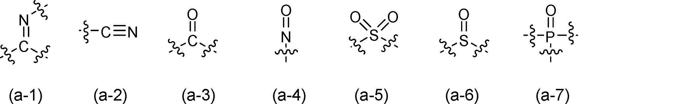

(前記一般式(b-1)~(b-6)において、
Rは、
水素原子、
置換もしくは無置換の環形成炭素数6~30のアリール基、
置換もしくは無置換の環形成原子数5~30の複素環基、または
置換もしくは無置換の炭素数1~30のアルキル基、である。
複数のRが存在する場合は互いに同じまたは異なる。複数のRは互いに結合して環を形成する場合と、しない場合とがある。)
Priority Applications (3)
| Application Number | Priority Date | Filing Date | Title |
|---|---|---|---|
| JP2014518737A JP5925308B2 (ja) | 2012-06-01 | 2013-05-30 | 有機エレクトロルミネッセンス素子 |
| EP13797623.9A EP2858136B1 (en) | 2012-06-01 | 2013-05-30 | Organic electroluminescence element and material for organic electroluminescence element |
| EP20206518.1A EP3809482A3 (en) | 2012-06-01 | 2013-05-30 | Organic electroluminescence element and material for organic electroluminescence element |
Applications Claiming Priority (4)
| Application Number | Priority Date | Filing Date | Title |
|---|---|---|---|
| JP2012126500 | 2012-06-01 | ||
| JP2012-126500 | 2012-06-01 | ||
| JP2012-221701 | 2012-10-03 | ||
| JP2012221701 | 2012-10-03 |
Publications (1)
| Publication Number | Publication Date |
|---|---|
| WO2013180241A1 true WO2013180241A1 (ja) | 2013-12-05 |
Family
ID=49673428
Family Applications (1)
| Application Number | Title | Priority Date | Filing Date |
|---|---|---|---|
| PCT/JP2013/065095 WO2013180241A1 (ja) | 2012-06-01 | 2013-05-30 | 有機エレクトロルミネッセンス素子および有機エレクトロルミネッセンス素子用材料 |
Country Status (5)
| Country | Link |
|---|---|
| US (2) | US9099658B2 (ja) |
| EP (2) | EP2858136B1 (ja) |
| JP (1) | JP5925308B2 (ja) |
| TW (1) | TWI554499B (ja) |
| WO (1) | WO2013180241A1 (ja) |
Cited By (27)
| Publication number | Priority date | Publication date | Assignee | Title |
|---|---|---|---|---|
| WO2015020217A1 (ja) * | 2013-08-09 | 2015-02-12 | 出光興産株式会社 | 有機エレクトロルミネッセンス用組成物、有機エレクトロルミネッセンス素子用材料、有機エレクトロルミネッセンス素子用材料溶液及び有機エレクトロルミネッセンス素子 |
| JP2015111624A (ja) * | 2013-12-06 | 2015-06-18 | コニカミノルタ株式会社 | 有機エレクトロルミネッセンス素子、発光性薄膜、表示装置及び照明装置 |
| WO2015098975A1 (ja) | 2013-12-26 | 2015-07-02 | 出光興産株式会社 | 有機エレクトロルミネッセンス素子および電子機器 |
| JP2016015487A (ja) * | 2014-07-01 | 2016-01-28 | ピョクサン ペイント アンド コーティングス カンパニー,リミテッド | 燐光ホスト用化合物及びこれを含んだ有機発光素子 |
| WO2016031785A1 (ja) * | 2014-08-26 | 2016-03-03 | 出光興産株式会社 | 有機エレクトロルミネッセンス素子および電子機器 |
| WO2016125807A1 (ja) * | 2015-02-06 | 2016-08-11 | 出光興産株式会社 | 有機エレクトロルミネッセンス素子および電子機器 |
| JP2016155797A (ja) * | 2014-12-30 | 2016-09-01 | 機光科技股▲分▼有限公司 | 有機材料およびそれを用いた有機エレクトロルミネッセンス素子 |
| JP2016157944A (ja) * | 2015-02-24 | 2016-09-01 | 株式会社半導体エネルギー研究所 | 発光素子、表示装置、電子機器、及び照明装置 |
| US9559311B2 (en) | 2013-02-22 | 2017-01-31 | Idemitsu Kosan Co., Ltd. | Anthracene derivative, organic-electroluminescence-device material, organic electroluminescence device, and electronic equipment |
| JP2017509164A (ja) * | 2014-03-13 | 2017-03-30 | メルク パテント ゲーエムベーハー | 有機エレクトロルミネッセント素子 |
| JP2017509165A (ja) * | 2014-03-13 | 2017-03-30 | メルク パテント ゲーエムベーハー | ルミネッセント化合物の調合物 |
| JPWO2016056559A1 (ja) * | 2014-10-07 | 2017-07-20 | 出光興産株式会社 | 有機エレクトロルミネッセンス素子、および電子機器 |
| WO2017146192A1 (ja) | 2016-02-24 | 2017-08-31 | 出光興産株式会社 | 有機エレクトロルミネッセンス素子、及び電子機器 |
| JP2017197482A (ja) * | 2016-04-28 | 2017-11-02 | コニカミノルタ株式会社 | π共役系化合物、有機エレクトロルミネッセンス素子材料、発光材料、電荷輸送材料、発光性薄膜、有機エレクトロルミネッセンス素子、表示装置及び照明装置 |
| US9997717B2 (en) | 2014-12-12 | 2018-06-12 | Idemitsu Kosan Co., Ltd. | Organic electroluminescence device and electronic device |
| WO2018181188A1 (ja) | 2017-03-31 | 2018-10-04 | 出光興産株式会社 | 有機エレクトロルミネッセンス素子および電子機器 |
| CN109790086A (zh) * | 2016-10-03 | 2019-05-21 | 出光兴产株式会社 | 化合物、组合物、有机电致发光元件及电子设备 |
| JP2020004717A (ja) * | 2018-06-25 | 2020-01-09 | 東レ株式会社 | 有機el表示装置 |
| US10651398B2 (en) | 2014-08-28 | 2020-05-12 | Idemitsu Kosan Co., Ltd. | Organic electroluminescence element and electronic device |
| JP2020141138A (ja) * | 2012-08-03 | 2020-09-03 | 株式会社半導体エネルギー研究所 | 発光装置 |
| JP2020167389A (ja) * | 2019-03-29 | 2020-10-08 | 住友化学株式会社 | 発光素子及びその製造方法並びに発光素子用組成物及びその製造方法 |
| US10978643B2 (en) * | 2014-12-19 | 2021-04-13 | Samsung Display Co., Ltd. | Organic light-emitting device |
| US11038113B2 (en) | 2014-11-19 | 2021-06-15 | Samsung Display Co., Ltd. | Organic light-emitting device |
| US11201297B2 (en) | 2018-03-19 | 2021-12-14 | Idemitsu Kosan Co., Ltd. | Organic electroluminescence device and electronic device |
| US11456425B2 (en) | 2015-12-28 | 2022-09-27 | Idemitsu Kosan Co., Ltd. | Organic electroluminescent element, and electronic apparatus |
| US11618722B2 (en) | 2016-11-09 | 2023-04-04 | Idemitsu Kosan Co., Ltd. | Compound, composition, organic electroluminescent element, and electronic appliance |
| US11957043B2 (en) | 2020-05-06 | 2024-04-09 | Samsung Display Co., Ltd. | Light-emitting device and electronic apparatus comprising same |
Families Citing this family (6)
| Publication number | Priority date | Publication date | Assignee | Title |
|---|---|---|---|---|
| CN101473464B (zh) | 2006-06-22 | 2014-04-23 | 出光兴产株式会社 | 应用含有杂环的芳胺衍生物的有机电致发光元件 |
| JP6513565B2 (ja) * | 2013-03-29 | 2019-05-22 | 株式会社Kyulux | 有機エレクトロルミネッセンス素子 |
| WO2016042781A1 (ja) | 2014-09-19 | 2016-03-24 | 出光興産株式会社 | 新規な化合物 |
| WO2016181705A1 (ja) * | 2015-05-11 | 2016-11-17 | 日本放送協会 | 有機薄膜および有機薄膜の製造方法、有機エレクトロルミネッセンス素子、表示装置、照明装置、有機薄膜太陽電池、薄膜トランジスタ、塗料組成物 |
| TWI814608B (zh) * | 2015-12-28 | 2023-09-01 | 國立大學法人九州大學 | 有機電致發光元件 |
| CN106977446A (zh) * | 2017-03-29 | 2017-07-25 | 江苏三月光电科技有限公司 | 一种以三苯并环庚烯酮为核心的化合物及其在oled器件上的应用 |
Citations (10)
| Publication number | Priority date | Publication date | Assignee | Title |
|---|---|---|---|---|
| WO2003080760A1 (fr) | 2002-03-22 | 2003-10-02 | Idemitsu Kosan Co., Ltd. | Materiau pour dispositifs electroluminescents organiques et dispositifs electroluminescents organiques produits avec ce materiau |
| WO2005091684A1 (ja) * | 2004-03-19 | 2005-09-29 | Idemitsu Kosan Co., Ltd. | 有機エレクトロルミネッセンス素子 |
| JP2009518342A (ja) * | 2005-12-08 | 2009-05-07 | メルク パテント ゲーエムベーハー | 有機エレクトロルミネセンス素子のための新規材料 |
| JP2010180204A (ja) | 2009-01-06 | 2010-08-19 | Fujifilm Corp | 電荷輸送材料及び有機電界発光素子 |
| WO2010134352A1 (ja) | 2009-05-22 | 2010-11-25 | 出光興産株式会社 | 有機エレクトロルミネッセンス素子 |
| WO2010134350A1 (ja) | 2009-05-22 | 2010-11-25 | 出光興産株式会社 | 有機エレクトロルミネッセンス素子 |
| WO2011070963A1 (ja) | 2009-12-07 | 2011-06-16 | 新日鐵化学株式会社 | 有機発光材料及び有機発光素子 |
| JP2011222831A (ja) * | 2010-04-12 | 2011-11-04 | Idemitsu Kosan Co Ltd | 有機エレクトロルミネッセンス素子 |
| JP2012079915A (ja) * | 2010-10-01 | 2012-04-19 | Toray Ind Inc | 発光素子材料および発光素子 |
| WO2012133188A1 (ja) * | 2011-03-25 | 2012-10-04 | 出光興産株式会社 | 有機エレクトロルミネッセンス素子 |
Family Cites Families (28)
| Publication number | Priority date | Publication date | Assignee | Title |
|---|---|---|---|---|
| TWI314947B (en) * | 2002-04-24 | 2009-09-21 | Eastman Kodak Compan | Organic light emitting diode devices with improved operational stability |
| EP1595933A4 (en) * | 2003-02-20 | 2009-04-08 | Idemitsu Kosan Co | FABRIC FOR ORGANIC ELECTROLUMINESCENZING DEVICE AND BASED ORGANIC ELECTROLUMINESCENSE DEVICE |
| JP4552436B2 (ja) * | 2003-12-24 | 2010-09-29 | コニカミノルタホールディングス株式会社 | 有機エレクトロルミネッセンス素子、表示装置及び照明装置 |
| KR100787425B1 (ko) * | 2004-11-29 | 2007-12-26 | 삼성에스디아이 주식회사 | 페닐카바졸계 화합물 및 이를 이용한 유기 전계 발광 소자 |
| KR100573137B1 (ko) * | 2004-04-02 | 2006-04-24 | 삼성에스디아이 주식회사 | 플루오렌계 화합물 및 이를 이용한 유기 전계 발광 소자 |
| EP1753271A4 (en) * | 2004-05-27 | 2009-01-28 | Idemitsu Kosan Co | WHITE ORGANIC ELECTROLUMINESCENT DEVICE |
| US20060088728A1 (en) * | 2004-10-22 | 2006-04-27 | Raymond Kwong | Arylcarbazoles as hosts in PHOLEDs |
| KR20070108392A (ko) * | 2005-03-04 | 2007-11-09 | 스미또모 가가꾸 가부시키가이샤 | 디카르바졸 방향족 아민 중합체 및 전자 장치 |
| CN101679337A (zh) * | 2007-05-21 | 2010-03-24 | 出光兴产株式会社 | 蒽衍生物以及利用该衍生物的有机电致发光元件 |
| WO2008156088A1 (ja) * | 2007-06-18 | 2008-12-24 | Idemitsu Kosan Co., Ltd. | トリナフチルモノアミン又はその誘導体及びそれを用いた有機エレクトロルミネッセンス素子、並びに有機エレクトロルミネッセンス材料含有溶液 |
| JP2009120582A (ja) * | 2007-10-26 | 2009-06-04 | Toyo Ink Mfg Co Ltd | カルバゾリル基を有する化合物およびその用途 |
| JP2009123976A (ja) * | 2007-11-16 | 2009-06-04 | Toyo Ink Mfg Co Ltd | 有機エレクトロルミネッセンス素子用材料および有機エレクトロルミネッセンス素子。 |
| KR20100097182A (ko) * | 2007-12-28 | 2010-09-02 | 이데미쓰 고산 가부시키가이샤 | 방향족 다이아민 유도체 및 그것을 이용한 유기 전기발광 소자 |
| KR100946411B1 (ko) * | 2008-03-28 | 2010-03-09 | 다우어드밴스드디스플레이머티리얼 유한회사 | 신규한 유기 발광 화합물 및 이를 발광재료로서 채용하고있는 유기 발광 소자 |
| KR100964232B1 (ko) * | 2008-09-03 | 2010-06-17 | 삼성모바일디스플레이주식회사 | 실리콘 함유 화합물 및 이를 이용한 유기 전계 발광 장치 |
| EP2423206B1 (en) * | 2009-04-24 | 2014-01-08 | Idemitsu Kosan Co., Ltd. | Aromatic amine derivative, and organic electroluminescent element comprising same |
| KR101754445B1 (ko) * | 2009-05-29 | 2017-07-05 | 이데미쓰 고산 가부시키가이샤 | 안트라센 유도체 및 그것을 이용한 유기 전계 발광 소자 |
| EP2471771B1 (en) * | 2009-08-28 | 2016-11-16 | Hodogaya Chemical Co., Ltd. | Compound having carbazole ring structure and organic electroluminescent device |
| US8617720B2 (en) | 2009-12-21 | 2013-12-31 | E I Du Pont De Nemours And Company | Electroactive composition and electronic device made with the composition |
| CN104592206B (zh) * | 2010-04-20 | 2019-12-31 | 出光兴产株式会社 | 双咔唑衍生物、有机电致发光元件用材料及使用其的有机电致发光元件 |
| JP2013201153A (ja) * | 2010-06-08 | 2013-10-03 | Idemitsu Kosan Co Ltd | 有機エレクトロルミネッセンス素子 |
| CN102884156B (zh) * | 2010-06-24 | 2016-01-20 | 东丽株式会社 | 发光元件材料和发光元件 |
| JP5814031B2 (ja) * | 2010-07-30 | 2015-11-17 | ユー・ディー・シー アイルランド リミテッド | 有機電界発光素子、及びジベンゾチオフェン構造又はジベンゾフラン構造を有する有機電界発光素子用材料 |
| CN102709485B (zh) | 2011-09-30 | 2016-05-25 | 昆山维信诺显示技术有限公司 | 一种有机电致发光器件及其制备方法 |
| CN107342368B (zh) * | 2011-11-22 | 2019-05-28 | 出光兴产株式会社 | 芳香族杂环衍生物、有机电致发光元件用材料以及有机电致发光元件 |
| KR101704150B1 (ko) * | 2011-12-05 | 2017-02-07 | 이데미쓰 고산 가부시키가이샤 | 유기 전기발광 소자용 재료 및 유기 전기발광 소자 |
| JP6060095B2 (ja) * | 2012-02-03 | 2017-01-11 | 出光興産株式会社 | カルバゾール化合物、有機エレクトロルミネッセンス素子用材料および有機エレクトロルミネッセンス素子 |
| WO2013129491A1 (ja) * | 2012-02-29 | 2013-09-06 | 出光興産株式会社 | 有機エレクトロルミネッセンス素子用材料及び有機エレクトロルミネッセンス素子 |
-
2013
- 2013-05-30 EP EP13797623.9A patent/EP2858136B1/en active Active
- 2013-05-30 JP JP2014518737A patent/JP5925308B2/ja active Active
- 2013-05-30 EP EP20206518.1A patent/EP3809482A3/en active Pending
- 2013-05-30 WO PCT/JP2013/065095 patent/WO2013180241A1/ja active Application Filing
- 2013-05-31 US US13/906,404 patent/US9099658B2/en not_active Ceased
- 2013-05-31 TW TW102119431A patent/TWI554499B/zh active
-
2017
- 2017-08-03 US US15/668,439 patent/USRE49343E1/en active Active
Patent Citations (10)
| Publication number | Priority date | Publication date | Assignee | Title |
|---|---|---|---|---|
| WO2003080760A1 (fr) | 2002-03-22 | 2003-10-02 | Idemitsu Kosan Co., Ltd. | Materiau pour dispositifs electroluminescents organiques et dispositifs electroluminescents organiques produits avec ce materiau |
| WO2005091684A1 (ja) * | 2004-03-19 | 2005-09-29 | Idemitsu Kosan Co., Ltd. | 有機エレクトロルミネッセンス素子 |
| JP2009518342A (ja) * | 2005-12-08 | 2009-05-07 | メルク パテント ゲーエムベーハー | 有機エレクトロルミネセンス素子のための新規材料 |
| JP2010180204A (ja) | 2009-01-06 | 2010-08-19 | Fujifilm Corp | 電荷輸送材料及び有機電界発光素子 |
| WO2010134352A1 (ja) | 2009-05-22 | 2010-11-25 | 出光興産株式会社 | 有機エレクトロルミネッセンス素子 |
| WO2010134350A1 (ja) | 2009-05-22 | 2010-11-25 | 出光興産株式会社 | 有機エレクトロルミネッセンス素子 |
| WO2011070963A1 (ja) | 2009-12-07 | 2011-06-16 | 新日鐵化学株式会社 | 有機発光材料及び有機発光素子 |
| JP2011222831A (ja) * | 2010-04-12 | 2011-11-04 | Idemitsu Kosan Co Ltd | 有機エレクトロルミネッセンス素子 |
| JP2012079915A (ja) * | 2010-10-01 | 2012-04-19 | Toray Ind Inc | 発光素子材料および発光素子 |
| WO2012133188A1 (ja) * | 2011-03-25 | 2012-10-04 | 出光興産株式会社 | 有機エレクトロルミネッセンス素子 |
Non-Patent Citations (13)
| Title |
|---|
| "Hikarikagaku no Sekai", 1993, CHEMICAL SOCIETY OF JAPAN, pages: 50 |
| "Organic EL Symposium, proceeding for the tenth meeting", 17 June 2010, article "Expression of Highly-Efficient Thermally-Activated Delayed-Fluorescence and Application thereof to OLED", pages: 11 - 12 |
| "Organic EL Symposium, proceeding for the tenth meeting", pages: 2 - 5,11-12 |
| "Organic Photochemical Reaction Theory", 1973, TOKYO KAGAKU DOJIN CO., LTD. |
| "proceeding for the 92nd spring meeting", 25 March 2012, CHEMICAL SOCIETY OF JAPAN, article "Development of Highly-Efficient Fluorescent EL Device Using Thermally-Activated Delayed-Fluorescence of Spiro-Skeleton Molecule", pages: 3M3 - 37 |
| D. YOKOYAMA ET AL., APPL. PHYS. LETT., vol. 93, 2008, pages 173302 |
| D. YOKOYAMA ET AL., APPL. PHYS. LETT., vol. 95, 2009, pages 243303 |
| D. YOKOYAMA ET AL., ORG. ELECTRON., vol. 10, 2009, pages 127 - 137 |
| J. KANG ET AL., INTERNATIONAL JOURNAL OF POLYMER SCIENCE, vol. 2010 |
| M. KASHA ET AL., PURE AND APPLIED CHEMISTRY, vol. 11, 1965, pages 371 |
| S. DAS ET AL., J. PHYS. CHEM. B., vol. 103, 1999, pages 209 |
| S. M. BACHILO ET AL., J. PHYS. CHEM. A, vol. 104, 2000, pages 7711 |
| See also references of EP2858136A4 |
Cited By (54)
| Publication number | Priority date | Publication date | Assignee | Title |
|---|---|---|---|---|
| JP2020141138A (ja) * | 2012-08-03 | 2020-09-03 | 株式会社半導体エネルギー研究所 | 発光装置 |
| JP2021022744A (ja) * | 2012-08-03 | 2021-02-18 | 株式会社半導体エネルギー研究所 | 発光素子、照明装置、発光装置および電子機器 |
| US11730007B2 (en) | 2012-08-03 | 2023-08-15 | Semiconductor Energy Laboratory Co., Ltd. | Light-emitting element |
| JP7030927B2 (ja) | 2012-08-03 | 2022-03-07 | 株式会社半導体エネルギー研究所 | 発光素子、照明装置、発光装置および電子機器 |
| US11355722B2 (en) | 2012-08-03 | 2022-06-07 | Semiconductor Energy Laboratory Co., Ltd. | Light-emitting element |
| US9559311B2 (en) | 2013-02-22 | 2017-01-31 | Idemitsu Kosan Co., Ltd. | Anthracene derivative, organic-electroluminescence-device material, organic electroluminescence device, and electronic equipment |
| JPWO2015020217A1 (ja) * | 2013-08-09 | 2017-03-02 | 出光興産株式会社 | 有機エレクトロルミネッセンス用組成物、有機エレクトロルミネッセンス素子用材料、有機エレクトロルミネッセンス素子用材料溶液及び有機エレクトロルミネッセンス素子 |
| US10833281B2 (en) | 2013-08-09 | 2020-11-10 | Idemitsu Kosan Co., Ltd. | Organic electroluminescence composition, material for organic electroluminescence element, solution of material for organic electroluminescence element, and organic electroluminescence element |
| WO2015020217A1 (ja) * | 2013-08-09 | 2015-02-12 | 出光興産株式会社 | 有機エレクトロルミネッセンス用組成物、有機エレクトロルミネッセンス素子用材料、有機エレクトロルミネッセンス素子用材料溶液及び有機エレクトロルミネッセンス素子 |
| JP2015111624A (ja) * | 2013-12-06 | 2015-06-18 | コニカミノルタ株式会社 | 有機エレクトロルミネッセンス素子、発光性薄膜、表示装置及び照明装置 |
| US9905779B2 (en) | 2013-12-26 | 2018-02-27 | Idemitsu Kosan Co., Ltd. | Organic electroluminescent element and electronic device |
| WO2015098975A1 (ja) | 2013-12-26 | 2015-07-02 | 出光興産株式会社 | 有機エレクトロルミネッセンス素子および電子機器 |
| US10811616B2 (en) | 2013-12-26 | 2020-10-20 | Idemitsu Kosan Co., Ltd. | Organic electroluminescent element and electronic device |
| KR20190083000A (ko) | 2013-12-26 | 2019-07-10 | 이데미쓰 고산 가부시키가이샤 | 유기 일렉트로 루미네센스 소자 및 전자 기기 |
| US11569456B2 (en) | 2013-12-26 | 2023-01-31 | Idemitsu Kosan Co., Ltd. | Organic electroluminescent element and electronic device |
| EP3879592A1 (en) | 2013-12-26 | 2021-09-15 | Idemitsu Kosan Co., Ltd. | Organic electroluminescent element and electronic device |
| KR20180020320A (ko) | 2013-12-26 | 2018-02-27 | 이데미쓰 고산 가부시키가이샤 | 유기 일렉트로 루미네센스 소자 및 전자 기기 |
| US11611046B2 (en) | 2014-03-13 | 2023-03-21 | Merck Patent Gmbh | Organic electroluminescent device |
| JP2017509165A (ja) * | 2014-03-13 | 2017-03-30 | メルク パテント ゲーエムベーハー | ルミネッセント化合物の調合物 |
| US10734587B2 (en) | 2014-03-13 | 2020-08-04 | Merck Patent Gmbh | Formulations of luminescent compounds |
| JP2017509164A (ja) * | 2014-03-13 | 2017-03-30 | メルク パテント ゲーエムベーハー | 有機エレクトロルミネッセント素子 |
| JP2016015487A (ja) * | 2014-07-01 | 2016-01-28 | ピョクサン ペイント アンド コーティングス カンパニー,リミテッド | 燐光ホスト用化合物及びこれを含んだ有機発光素子 |
| KR102437253B1 (ko) * | 2014-08-26 | 2022-08-26 | 이데미쓰 고산 가부시키가이샤 | 유기 일렉트로 루미네선스 소자 및 전자 기기 |
| US9947876B2 (en) | 2014-08-26 | 2018-04-17 | Idemitsu Kosan Co., Ltd. | Organic electroluminescence device and electronic device |
| WO2016031785A1 (ja) * | 2014-08-26 | 2016-03-03 | 出光興産株式会社 | 有機エレクトロルミネッセンス素子および電子機器 |
| US20160301014A1 (en) * | 2014-08-26 | 2016-10-13 | Idemitsu Kosan Co., Ltd. | Organic electroluminescence device and electronic device |
| KR20170083960A (ko) * | 2014-08-26 | 2017-07-19 | 이데미쓰 고산 가부시키가이샤 | 유기 일렉트로 루미네선스 소자 및 전자 기기 |
| JPWO2016031785A1 (ja) * | 2014-08-26 | 2017-06-08 | 出光興産株式会社 | 有機エレクトロルミネッセンス素子および電子機器 |
| US10651398B2 (en) | 2014-08-28 | 2020-05-12 | Idemitsu Kosan Co., Ltd. | Organic electroluminescence element and electronic device |
| US11043638B2 (en) | 2014-10-07 | 2021-06-22 | Idemitsu Kosan Co., Ltd. | Organic electroluminescence device and electronic device |
| JPWO2016056559A1 (ja) * | 2014-10-07 | 2017-07-20 | 出光興産株式会社 | 有機エレクトロルミネッセンス素子、および電子機器 |
| US11038113B2 (en) | 2014-11-19 | 2021-06-15 | Samsung Display Co., Ltd. | Organic light-emitting device |
| US9997717B2 (en) | 2014-12-12 | 2018-06-12 | Idemitsu Kosan Co., Ltd. | Organic electroluminescence device and electronic device |
| US10978643B2 (en) * | 2014-12-19 | 2021-04-13 | Samsung Display Co., Ltd. | Organic light-emitting device |
| JP2016155797A (ja) * | 2014-12-30 | 2016-09-01 | 機光科技股▲分▼有限公司 | 有機材料およびそれを用いた有機エレクトロルミネッセンス素子 |
| CN107112431A (zh) * | 2015-02-06 | 2017-08-29 | 出光兴产株式会社 | 有机电致发光元件和电子设备 |
| CN107112431B (zh) * | 2015-02-06 | 2019-08-23 | 出光兴产株式会社 | 有机电致发光元件和电子设备 |
| WO2016125807A1 (ja) * | 2015-02-06 | 2016-08-11 | 出光興産株式会社 | 有機エレクトロルミネッセンス素子および電子機器 |
| US10351765B2 (en) | 2015-02-06 | 2019-07-16 | Idemitsu Kosan Co., Ltd. | Organic electroluminescence element and electronic device |
| US10125310B2 (en) | 2015-02-06 | 2018-11-13 | Idemitsu Kosan Co., Ltd. | Organic electroluminescence element and electronic device |
| JPWO2016125807A1 (ja) * | 2015-02-06 | 2017-11-24 | 出光興産株式会社 | 有機エレクトロルミネッセンス素子および電子機器 |
| JP2016157944A (ja) * | 2015-02-24 | 2016-09-01 | 株式会社半導体エネルギー研究所 | 発光素子、表示装置、電子機器、及び照明装置 |
| US11456425B2 (en) | 2015-12-28 | 2022-09-27 | Idemitsu Kosan Co., Ltd. | Organic electroluminescent element, and electronic apparatus |
| WO2017146192A1 (ja) | 2016-02-24 | 2017-08-31 | 出光興産株式会社 | 有機エレクトロルミネッセンス素子、及び電子機器 |
| JP2017197482A (ja) * | 2016-04-28 | 2017-11-02 | コニカミノルタ株式会社 | π共役系化合物、有機エレクトロルミネッセンス素子材料、発光材料、電荷輸送材料、発光性薄膜、有機エレクトロルミネッセンス素子、表示装置及び照明装置 |
| US11271164B2 (en) | 2016-10-03 | 2022-03-08 | Idemitsu Kosan Co., Ltd | Compound, composition, organic electroluminescent element and electronic device |
| CN109790086A (zh) * | 2016-10-03 | 2019-05-21 | 出光兴产株式会社 | 化合物、组合物、有机电致发光元件及电子设备 |
| US11618722B2 (en) | 2016-11-09 | 2023-04-04 | Idemitsu Kosan Co., Ltd. | Compound, composition, organic electroluminescent element, and electronic appliance |
| WO2018181188A1 (ja) | 2017-03-31 | 2018-10-04 | 出光興産株式会社 | 有機エレクトロルミネッセンス素子および電子機器 |
| US11201297B2 (en) | 2018-03-19 | 2021-12-14 | Idemitsu Kosan Co., Ltd. | Organic electroluminescence device and electronic device |
| JP2020004717A (ja) * | 2018-06-25 | 2020-01-09 | 東レ株式会社 | 有機el表示装置 |
| JP7310349B2 (ja) | 2018-06-25 | 2023-07-19 | 東レ株式会社 | 有機el表示装置 |
| JP2020167389A (ja) * | 2019-03-29 | 2020-10-08 | 住友化学株式会社 | 発光素子及びその製造方法並びに発光素子用組成物及びその製造方法 |
| US11957043B2 (en) | 2020-05-06 | 2024-04-09 | Samsung Display Co., Ltd. | Light-emitting device and electronic apparatus comprising same |
Also Published As
| Publication number | Publication date |
|---|---|
| JP5925308B2 (ja) | 2016-05-25 |
| TW201406724A (zh) | 2014-02-16 |
| EP2858136A1 (en) | 2015-04-08 |
| US9099658B2 (en) | 2015-08-04 |
| US20150115225A1 (en) | 2015-04-30 |
| JPWO2013180241A1 (ja) | 2016-01-21 |
| EP3809482A2 (en) | 2021-04-21 |
| TWI554499B (zh) | 2016-10-21 |
| EP3809482A3 (en) | 2021-10-27 |
| USRE49343E1 (en) | 2022-12-20 |
| EP2858136B1 (en) | 2021-05-26 |
| EP2858136A4 (en) | 2016-10-05 |
Similar Documents
| Publication | Publication Date | Title |
|---|---|---|
| JP5925308B2 (ja) | 有機エレクトロルミネッセンス素子 | |
| US11322711B2 (en) | Organic EL light emitting apparatus and electronic instrument | |
| JP6434073B2 (ja) | 有機エレクトロルミネッセンス素子 | |
| JP6129075B2 (ja) | ビスカルバゾール誘導体およびこれを用いた有機エレクトロルミネッセンス素子 | |
| JP6088979B2 (ja) | 芳香族複素環誘導体、有機エレクトロルミネッセンス素子用材料および有機エレクトロルミネッセンス素子 | |
| JP6424002B2 (ja) | 有機エレクトロルミネッセンス素子および有機エレクトロルミネッセンス素子用材料 | |
| JP6101248B2 (ja) | 新規化合物、有機エレクトロルミネッセンス素子用材料および有機エレクトロルミネッセンス素子 | |
| EP2372803A1 (en) | Material for organic electroluminescent element, and organic electroluminescent element | |
| JP6060095B2 (ja) | カルバゾール化合物、有機エレクトロルミネッセンス素子用材料および有機エレクトロルミネッセンス素子 | |
| WO2013147205A1 (ja) | 有機エレクトロルミネッセンス素子および有機エレクトロルミネッセンス素子用材料 | |
| JP6034005B2 (ja) | ビスカルバゾール誘導体およびこれを用いた有機エレクトロルミネッセンス素子 |
Legal Events
| Date | Code | Title | Description |
|---|---|---|---|
| 121 | Ep: the epo has been informed by wipo that ep was designated in this application |
Ref document number: 13797623 Country of ref document: EP Kind code of ref document: A1 |
|
| ENP | Entry into the national phase |
Ref document number: 2014518737 Country of ref document: JP Kind code of ref document: A |
|
| NENP | Non-entry into the national phase |
Ref country code: DE |
|
| WWE | Wipo information: entry into national phase |
Ref document number: 2013797623 Country of ref document: EP |