WO2010098349A1 - Ledランプ - Google Patents
Ledランプ Download PDFInfo
- Publication number
- WO2010098349A1 WO2010098349A1 PCT/JP2010/052870 JP2010052870W WO2010098349A1 WO 2010098349 A1 WO2010098349 A1 WO 2010098349A1 JP 2010052870 W JP2010052870 W JP 2010052870W WO 2010098349 A1 WO2010098349 A1 WO 2010098349A1
- Authority
- WO
- WIPO (PCT)
- Prior art keywords
- led
- led module
- lamp according
- modules
- led lamp
- Prior art date
- Legal status (The legal status is an assumption and is not a legal conclusion. Google has not performed a legal analysis and makes no representation as to the accuracy of the status listed.)
- Ceased
Links
Images


























Classifications
-
- F—MECHANICAL ENGINEERING; LIGHTING; HEATING; WEAPONS; BLASTING
- F21—LIGHTING
- F21K—NON-ELECTRIC LIGHT SOURCES USING LUMINESCENCE; LIGHT SOURCES USING ELECTROCHEMILUMINESCENCE; LIGHT SOURCES USING CHARGES OF COMBUSTIBLE MATERIAL; LIGHT SOURCES USING SEMICONDUCTOR DEVICES AS LIGHT-GENERATING ELEMENTS; LIGHT SOURCES NOT OTHERWISE PROVIDED FOR
- F21K9/00—Light sources using semiconductor devices as light-generating elements, e.g. using light-emitting diodes [LED] or lasers
- F21K9/20—Light sources comprising attachment means
- F21K9/23—Retrofit light sources for lighting devices with a single fitting for each light source, e.g. for substitution of incandescent lamps with bayonet or threaded fittings
- F21K9/233—Retrofit light sources for lighting devices with a single fitting for each light source, e.g. for substitution of incandescent lamps with bayonet or threaded fittings specially adapted for generating a spot light distribution, e.g. for substitution of reflector lamps
-
- F—MECHANICAL ENGINEERING; LIGHTING; HEATING; WEAPONS; BLASTING
- F21—LIGHTING
- F21K—NON-ELECTRIC LIGHT SOURCES USING LUMINESCENCE; LIGHT SOURCES USING ELECTROCHEMILUMINESCENCE; LIGHT SOURCES USING CHARGES OF COMBUSTIBLE MATERIAL; LIGHT SOURCES USING SEMICONDUCTOR DEVICES AS LIGHT-GENERATING ELEMENTS; LIGHT SOURCES NOT OTHERWISE PROVIDED FOR
- F21K9/00—Light sources using semiconductor devices as light-generating elements, e.g. using light-emitting diodes [LED] or lasers
- F21K9/20—Light sources comprising attachment means
- F21K9/27—Retrofit light sources for lighting devices with two fittings for each light source, e.g. for substitution of fluorescent tubes
-
- F—MECHANICAL ENGINEERING; LIGHTING; HEATING; WEAPONS; BLASTING
- F21—LIGHTING
- F21K—NON-ELECTRIC LIGHT SOURCES USING LUMINESCENCE; LIGHT SOURCES USING ELECTROCHEMILUMINESCENCE; LIGHT SOURCES USING CHARGES OF COMBUSTIBLE MATERIAL; LIGHT SOURCES USING SEMICONDUCTOR DEVICES AS LIGHT-GENERATING ELEMENTS; LIGHT SOURCES NOT OTHERWISE PROVIDED FOR
- F21K9/00—Light sources using semiconductor devices as light-generating elements, e.g. using light-emitting diodes [LED] or lasers
- F21K9/60—Optical arrangements integrated in the light source, e.g. for improving the colour rendering index or the light extraction
- F21K9/68—Details of reflectors forming part of the light source
-
- H—ELECTRICITY
- H10—SEMICONDUCTOR DEVICES; ELECTRIC SOLID-STATE DEVICES NOT OTHERWISE PROVIDED FOR
- H10H—INORGANIC LIGHT-EMITTING SEMICONDUCTOR DEVICES HAVING POTENTIAL BARRIERS
- H10H20/00—Individual inorganic light-emitting semiconductor devices having potential barriers, e.g. light-emitting diodes [LED]
- H10H20/80—Constructional details
- H10H20/85—Packages
- H10H20/852—Encapsulations
- H10H20/853—Encapsulations characterised by their shape
-
- H—ELECTRICITY
- H10—SEMICONDUCTOR DEVICES; ELECTRIC SOLID-STATE DEVICES NOT OTHERWISE PROVIDED FOR
- H10H—INORGANIC LIGHT-EMITTING SEMICONDUCTOR DEVICES HAVING POTENTIAL BARRIERS
- H10H20/00—Individual inorganic light-emitting semiconductor devices having potential barriers, e.g. light-emitting diodes [LED]
- H10H20/80—Constructional details
- H10H20/85—Packages
- H10H20/855—Optical field-shaping means, e.g. lenses
- H10H20/856—Reflecting means
-
- H—ELECTRICITY
- H10—SEMICONDUCTOR DEVICES; ELECTRIC SOLID-STATE DEVICES NOT OTHERWISE PROVIDED FOR
- H10H—INORGANIC LIGHT-EMITTING SEMICONDUCTOR DEVICES HAVING POTENTIAL BARRIERS
- H10H20/00—Individual inorganic light-emitting semiconductor devices having potential barriers, e.g. light-emitting diodes [LED]
- H10H20/80—Constructional details
- H10H20/85—Packages
- H10H20/857—Interconnections, e.g. lead-frames, bond wires or solder balls
-
- H—ELECTRICITY
- H10—SEMICONDUCTOR DEVICES; ELECTRIC SOLID-STATE DEVICES NOT OTHERWISE PROVIDED FOR
- H10W—GENERIC PACKAGES, INTERCONNECTIONS, CONNECTORS OR OTHER CONSTRUCTIONAL DETAILS OF DEVICES COVERED BY CLASS H10
- H10W90/00—Package configurations
-
- F—MECHANICAL ENGINEERING; LIGHTING; HEATING; WEAPONS; BLASTING
- F21—LIGHTING
- F21Y—INDEXING SCHEME ASSOCIATED WITH SUBCLASSES F21K, F21L, F21S and F21V, RELATING TO THE FORM OR THE KIND OF THE LIGHT SOURCES OR OF THE COLOUR OF THE LIGHT EMITTED
- F21Y2103/00—Elongate light sources, e.g. fluorescent tubes
- F21Y2103/10—Elongate light sources, e.g. fluorescent tubes comprising a linear array of point-like light-generating elements
-
- F—MECHANICAL ENGINEERING; LIGHTING; HEATING; WEAPONS; BLASTING
- F21—LIGHTING
- F21Y—INDEXING SCHEME ASSOCIATED WITH SUBCLASSES F21K, F21L, F21S and F21V, RELATING TO THE FORM OR THE KIND OF THE LIGHT SOURCES OR OF THE COLOUR OF THE LIGHT EMITTED
- F21Y2105/00—Planar light sources
- F21Y2105/10—Planar light sources comprising a two-dimensional [2D] array of point-like light-generating elements
-
- F—MECHANICAL ENGINEERING; LIGHTING; HEATING; WEAPONS; BLASTING
- F21—LIGHTING
- F21Y—INDEXING SCHEME ASSOCIATED WITH SUBCLASSES F21K, F21L, F21S and F21V, RELATING TO THE FORM OR THE KIND OF THE LIGHT SOURCES OR OF THE COLOUR OF THE LIGHT EMITTED
- F21Y2115/00—Light-generating elements of semiconductor light sources
- F21Y2115/10—Light-emitting diodes [LED]
-
- H—ELECTRICITY
- H10—SEMICONDUCTOR DEVICES; ELECTRIC SOLID-STATE DEVICES NOT OTHERWISE PROVIDED FOR
- H10H—INORGANIC LIGHT-EMITTING SEMICONDUCTOR DEVICES HAVING POTENTIAL BARRIERS
- H10H20/00—Individual inorganic light-emitting semiconductor devices having potential barriers, e.g. light-emitting diodes [LED]
- H10H20/80—Constructional details
- H10H20/85—Packages
- H10H20/855—Optical field-shaping means, e.g. lenses
-
- H—ELECTRICITY
- H10—SEMICONDUCTOR DEVICES; ELECTRIC SOLID-STATE DEVICES NOT OTHERWISE PROVIDED FOR
- H10W—GENERIC PACKAGES, INTERCONNECTIONS, CONNECTORS OR OTHER CONSTRUCTIONAL DETAILS OF DEVICES COVERED BY CLASS H10
- H10W90/00—Package configurations
- H10W90/701—Package configurations characterised by the relative positions of pads or connectors relative to package parts
- H10W90/751—Package configurations characterised by the relative positions of pads or connectors relative to package parts of bond wires
- H10W90/754—Package configurations characterised by the relative positions of pads or connectors relative to package parts of bond wires between a chip and a stacked insulating package substrate, interposer or RDL
Definitions
- the present invention relates to an LED lamp using a light emitting diode (hereinafter, LED) as a light source.
- LED light emitting diode
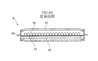
- FIG. 63 shows an example of a conventional LED lamp (for example, see Patent Document 1).
- the LED lamp X shown in the figure includes a plate-like substrate 91, a plurality of LED modules 92 mounted on the substrate 91, a heat dissipation member 95 attached to the substrate 91, and a case 93 that accommodates the substrate 91. And a terminal 94.
- a wiring pattern (not shown) connected to the plurality of LED modules 92 and the terminals 94 is formed on the substrate 91.
- This LED lamp X is configured such that a plurality of LED modules 92 can emit light by fitting a terminal 94 into a socket of a general fluorescent lamp lighting fixture.
- the general-use fluorescent lamp luminaire is a luminaire widely used mainly for indoor general illumination.
- a commercial power supply for example, AC 100V
- a straight pipe defined in JIS C7617 This refers to a lighting fixture to which a circular fluorescent lamp or an annular fluorescent lamp defined in JIS C7618 is attached (hereinafter, “general fluorescent lamp lighting fixture” is simply referred to as “lighting fixture”).
- the main emission direction of the LED module 92 faces downward.
- the light from the LED module 92 is emitted mainly in the main emission direction of the LED module 92. Therefore, sufficient brightness may not be obtained around the LED lamp X, particularly in the vicinity of the side.
- the LED lamp X has a problem that it is difficult to obtain sufficient brightness particularly in the vicinity of the side as compared with when the general fluorescent lamp is turned on.
- the present invention has been conceived under the circumstances described above, and an object thereof is to provide an LED lamp capable of illuminating the surroundings with sufficient brightness.
- the LED lamp provided by the present invention includes a plurality of LED modules each having an LED chip, and a support member having a support surface on which the plurality of LED modules are mounted. It is characterized by being constituted by a plurality of types of LED modules having different directivity characteristics that are luminous intensity distributions in the emission direction.
- the plurality of LED modules includes a first LED module located near the center of the support surface, and the first LED module is more than the other LED modules. It has a directivity characteristic in which the light intensity distribution is biased in the normal direction of the support surface.
- the first LED module includes a reflector that surrounds the LED chip and opens in the normal direction.
- the first LED module further includes a sealing resin for sealing the LED chip, and the sealing resin is filled in a space surrounded by the reflector. ing.
- the dimension of the support member in the normal direction of the support surface is smaller than the dimension of the support surface in the in-plane direction.
- the first LED module includes a substrate on which the LED chip is mounted, and on the surface of the substrate opposite to the surface on which the LED chip is mounted, Mounting terminals are provided.
- the plurality of LED modules include a second LED module positioned near an end of the support surface, and the second LED module is more than the other LED modules. It has directivity characteristics in which the luminous intensity distribution is biased outward in the in-plane direction of the support surface.
- the second LED module includes a reflector that surrounds the LED chip and opens outward in the in-plane direction.
- the second LED module further includes a sealing resin for sealing the LED chip, and the sealing resin is filled in a space surrounded by the reflector. ing.
- the second LED module includes a substrate on which the LED chip is mounted, and the side surface of the substrate and the support surface of the support member face each other. It is mounted on the support member.
- the second LED module has a dimension in the in-plane direction of the support member larger than a dimension in the normal direction of the support member.
- the plurality of LED modules are located between the first and second LED modules, and the luminous intensity distribution in the emission direction is more uniform than the first and second LED modules.
- a third LED module having directional characteristics is further included.
- the third LED module includes a substrate on which the LED chip is mounted, and on the surface of the substrate opposite to the surface on which the LED chip is mounted, Mounting terminals are provided.
- the said 3rd LED module is provided with sealing resin which seals the said LED chip, and the said sealing resin is the normal line direction of the said support surface, and an in-plane direction, respectively. Is exposed.
- the support surface has a strip shape
- the plurality of first LED modules are arranged along the longitudinal direction near the center of the support surface
- the plurality of second LED modules Are arranged along both ends in the width direction of the support surface
- the plurality of third LED modules are arranged along the longitudinal direction in a region sandwiched between the plurality of first and second LED modules.
- the case has a cylindrical shape.
- the support member is an insulating substrate, and further includes a heat dissipating member joined to a portion of the insulating substrate opposite to the support surface.
- the case is formed with a protruding piece that protrudes inward and supports the substrate.
- the protruding piece is engaged with the heat radiating member.
- FIG. 2 is a cross-sectional view of a main part taken along line II-II in FIG. It is a top view which shows a 1st LED module.
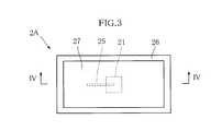
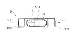
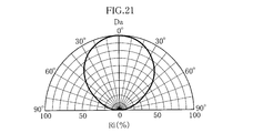
- FIG. 4 is a cross-sectional view of a principal part taken along line IV-IV in FIG. 3. It is a bottom view which shows a 1st LED module. It is a figure which shows the directional characteristic of a 1st LED module. It is a side view which shows a 2nd LED module.
- FIG. 8 is a cross-sectional view of a principal part taken along line VIII-VIII in FIG. It is a figure which shows the state in which the 2nd LED module was mounted in the support substrate.
- FIG. 12 is a main part cross-sectional view taken along line XII-XII in FIG. 11. It is a figure which shows the directional characteristic of the 2nd LED module of a modification. It is a top view which shows a 3rd LED module.
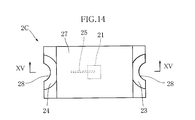
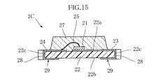
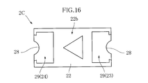
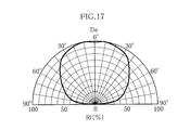
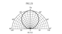
- FIG. 15 is a main part cross-sectional view taken along line XV-XV in FIG. 14. It is a bottom view which shows a 3rd LED module. It is a figure which shows the directional characteristic of a 3rd LED module. It is a figure for demonstrating the effect
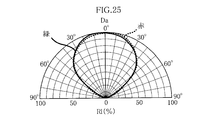
- FIG. 25 is a diagram showing directivity characteristics of the first LED module shown in FIG. 24 that emits red and green light.
- FIG. 25 is a diagram showing directional characteristics of the first LED module shown in FIG. 24 that emits blue and red light.
- FIG. 60 is a diagram showing directivity characteristics of the LED module shown in FIG. 59. It is a side view which shows the modification of an LED module.
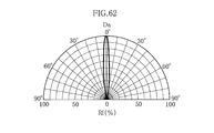
- FIG. 62 is a diagram showing directivity characteristics of the LED module shown in FIG. 61. It is sectional drawing which shows an example of the conventional LED lamp.
- FIG. 1 and 2 are diagrams showing an example of an LED lamp according to the present invention.
- FIG. 1 is a perspective view of the main part of the LED lamp
- FIG. 2 is a cross-sectional view of the main part along the line II-II in FIG.
- the LED lamp A of this embodiment includes a support substrate 1, a plurality of LED modules 2, a heat radiating member 3, a case 4, and a pair of caps 5.
- This LED lamp A is used, for example, as an alternative to a straight tube fluorescent lamp attached to a general fluorescent lamp luminaire.
- the LED lamp A is usually mounted so that the main emission direction of the LED module 2 faces downward.
- the support substrate 1 supports a plurality of LED modules 2.
- the support substrate 1 is made of, for example, glass epoxy resin and is formed in a long and narrow plate shape.
- a wiring pattern (not shown) made of Cu, for example, for supplying power to the plurality of LED modules 2 is formed on the mounting surface 1 a of the support substrate 1.
- the plurality of LED modules 2 are arranged in a matrix on the mounting surface 1a as shown in FIG.
- sequence and number of LED modules 2 on the mounting surface 1a of the support substrate 1 shown in FIG. 1 are examples, and are not limited to this.
- the LED module 2 includes first to third LED modules 2A, 2B, and 2C.
- the first to third LED modules 2A, 2B, and 2C have different light intensity distributions (directivity characteristics).
- the first LED module 2A includes an LED chip 21, a substrate 22, metal wiring patterns 23 and 24 that are separated from each other, wires 25, a frame body 26, and a sealing resin 27.
- the first LED module 2A has a length of about 1.6 mm, a width of about 0.8 mm, and a thickness of about 0.55 mm.
- the thickness which is a dimension in the normal direction of the mounting surface 1a, is the thickness of the mounting surface 1a. It is smaller than the length and width which are dimensions in the in-plane direction.
- the first LED module 2A has directivity characteristics in which the light emitted from the LED chip 21 has a light intensity distribution biased in the normal direction of the mounting surface 1a of the support substrate 1.
- a plurality of first LED modules 2 ⁇ / b> A are linearly arranged along the longitudinal direction of the support substrate 1, for example, at the center of the support substrate 1.
- Each first LED module 2A is arranged such that the main emission direction of the LED chip 21 coincides with the normal direction of the mounting surface 1a.
- the LED chip 21 is mounted on the mounting surface 22 a of the substrate 22 via the wiring patterns 23 and 24.
- the LED chip 21 has a structure in which, for example, an n-type semiconductor and a p-type semiconductor and an active layer (both not shown) sandwiched between them are stacked.
- the LED chip 21 when the LED chip 21 is made of a GaN-based semiconductor, the LED chip 21 can emit blue light.
- the LED chip 21 has two electrodes (not shown) on the upper and lower surfaces.
- the electrode on the lower surface of the LED chip 21 is electrically connected to the wiring pattern 23.
- the wiring pattern 23 reaches the back surface 22 b of the substrate 22 through the inner surface of the concave portion 28 that is substantially semicircular in sectional view.
- the wiring pattern 23 on the back surface 22 b is a mounting terminal 29 that is bonded to a wiring pattern (not shown) of the support substrate 1.
- the electrode on the upper surface of the LED chip 21 is connected to the wiring pattern 2324 through the wire 25. Thereby, the electrode on the upper surface of the LED chip 21 is electrically connected to the wiring pattern 2324.
- the wiring pattern 2324 reaches the back surface 22 b of the substrate 22 through the recess 28, and the lead 24 on the back surface 22 b is a mounting terminal 29 that is bonded to the wiring pattern of the support substrate 1. .
- the frame body 26 is made of, for example, white resin and is formed to extend upward from the outer peripheral portion of the mounting surface 22a.
- the frame body 26 has a reflective surface 26 a surrounding the LED chip 21, the wire 25, and the sealing resin 27.
- the reflecting surface 26a is for reflecting upward the light emitted from the LED chip 21 to be directed upward. That is, the first LED module 2A is an LED module with a so-called reflector. Thereby, as for the 1st LED module 2A, the luminous intensity which the light from LED chip 21 goes to the normal line direction of the mounting surface 1a of the support substrate 1 is made large.
- Sealing resin 27 is for protecting LED chip 21 and wire 25.
- the sealing resin 27 is formed using, for example, a silicon resin that has translucency with respect to light emitted from the LED chip 21.
- a fluorescent material that emits yellow light when excited by blue light is mixed in the sealing resin 27, white light can be emitted from the LED module 2.
- fluorescent materials that emit green light and red light may be mixed.
- the second LED module 2B has a length of about 3.8 mm, a width of about 1 mm, and a thickness of about 0.6 mm.
- the thickness which is the dimension in the normal direction of the mounting surface 1a, is in the plane of the mounting surface 1a. It is smaller than the length and width which are dimensions in the direction.
- the leads 23 and 24 extend from the mounting surface 22a of the substrate 22 to the side surface 22c.
- the portions of the leads 23 and 24 that cover the side surface 22 c are the mounting terminals 29.
- the second LED module 2 ⁇ / b> B is arranged with respect to the support substrate 1 so that the substrate 22 is tilted sideways, and the mounting terminals 29 are connected to the wiring pattern (not shown) of the support substrate 1 by the solder 30. It is mounted on the support substrate 1 by being bonded.
- the second LED module 2 ⁇ / b> B has the main emission direction of the LED chip 21 coincident with the in-plane direction of the mounting surface 1 a of the support substrate 1.
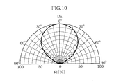
- FIG. 10 shows the directivity characteristics of the second LED module 2B.
- the relative luminous intensity ratio Rl is directed to the maximum at the directivity angle of 0 °, that is, outward in the in-plane direction of the mounting surface 1a.
- a plurality of second LED modules 2 ⁇ / b> B are arranged along both end portions in the width direction of the support substrate 1.
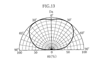
- the frame body 26 is not provided, that is, the second LED module 2B ′ in which the reflector is omitted may be employed.
- the sealing resin 27 is formed in a substantially trapezoidal shape in a side view.
- the leads 23 and 24 extend from the mounting surface 22a of the substrate 22 to the back surface 22b via the side surface 22c.
- the leads 23 and 24 on the side surface 22c are the mounting terminals 29, respectively.
- FIG. 13 shows the directivity characteristics of the second LED module 2B ′. Compared with the 2nd LED module 2B, the relative luminous intensity ratio Rl in a wider area
- the third LED module 2C has a length of about 1.6 mm, a width of about 0.8 mm, and a thickness of about 0.36 mm.
- the thickness that is the dimension in the normal direction of the mounting surface 1a is the thickness of the mounting surface 1a. It is smaller than the length and width which are dimensions in the in-plane direction.
- the third LED module 2C is different from the first and second LED modules 2A and 2B in that the frame body 26 is not provided on the substrate 22. That is, as shown in FIG. 15, in the third LED module 2C, the sealing resin 27 is formed in a substantially trapezoidal shape in a side view, and most of the resin is exposed to the outside. Therefore, in the third LED module 2C, the light from the LED chip 21 is emitted not only in the main emission direction but also in a relatively large proportion not only in the oblique direction but also in the lateral direction.
- a plurality of third LED modules 2C are straight in a region sandwiched between a plurality of first LED modules 2A and a plurality of second LED modules 2B on the mounting surface 1a. Arranged in a shape.
- Each third LED module 2 ⁇ / b> C is arranged so that the main emission direction of the LED chip 21 coincides with the direction orthogonal to the mounting surface 1 a of the support substrate 1.
- the heat radiating member 3 is for dissipating heat generated in the LED module 2, and is attached to the back side of the support substrate 1.
- the heat dissipating member 3 is made of, for example, Al, and is formed in an elongated block shape extending along the longitudinal direction of the support substrate 1.
- the heat radiating member 3 you may mount and support the LED module 2 directly by giving an insulating process to the surface. That is, the support substrate 1 may be omitted. In this case, a wiring pattern similar to the wiring pattern formed on the mounting surface 1a of the support substrate 1 is formed between the LED module 2 and an insulating sheet (not shown) having an insulating function, for example. According to this configuration, it is not necessary to prepare the support substrate 1 for mounting the LED module 2 separately from the heat radiating member 3, so that the cost of components can be reduced.
- the case 4 is for accommodating the support substrate 1, the heat radiating member 3, and the like, and has a cylindrical shape as shown in FIG.
- the case 4 is made of a synthetic resin such as polycarbonate, and is integrally formed by extrusion molding. When part of the light from the LED module 2 reaches the inner surface of the case 4, the case 4 transmits the light while diffusing.
- a pair of projecting pieces 41 projecting inward are integrally formed on the inner surface of the case 4.
- the heat radiating member 3 is restricted from moving in a direction perpendicular to the central axis O ⁇ b> 1 (upward in the figure) with respect to the case 4 by a part of the heat radiating member 3 abutting against the protruding piece 41.
- the heat radiating member 3 is inserted into the case 4 while sliding inside the protruding piece 41.
- the pair of caps 5 is for supplying AC power from a commercial power source by being mounted on a socket (not shown) of a general fluorescent lamp luminaire.
- the base 5 includes two terminals 51.
- the terminal 51 is a part that fits into the socket of the general fluorescent lamp lighting fixture.
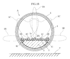
- FIG. 18 shows a cross-sectional state of the LED lamp A attached to a general fluorescent lamp illuminator installed on the indoor ceiling P, for example, and the top and bottom are reversed in FIG.
- a dotted line SA indicates the directivity characteristic of the first LED module 2A.
- the first LED module 2A has a directivity characteristic in which the luminous intensity distribution is extremely biased in the normal direction of the mounting surface 1a.
- a dotted line SB indicates the directivity characteristic of the second LED module 2B.
- the second LED module 2B has directivity characteristics in which the light intensity distribution is biased outward in the in-plane direction of the mounting surface 1a.
- the dotted line SC has the directivity characteristic of the third LED module 2C.
- the third LED module 2C has a relatively uniform directivity characteristic around the normal direction of the mounting surface 1a.
- or 3rd LED modules 2A, 2B, 2C from which the directivity characteristics of light mutually differ are distribute
- the light emitted from LED lamp A is Except for the ceiling P side, it is irradiated almost uniformly toward its periphery. Therefore, sufficient brightness can be obtained in the entire periphery of the LED lamp A.
- the LED lamp according to the present invention is not limited to the embodiment described above.
- the specific configuration of each part of the LED lamp according to the present invention can be varied in design in various ways.
- the shapes of the support substrate 1, the LED module 2, the heat radiating member 3, the case 4 and the like are not limited to the above-described shapes.
- the mounting form of each LED module 2 mounted on the support substrate 1 is not limited to the above-described embodiment.
- the movement of the heat radiating member 3 is restricted by the pair of projecting pieces 41 projecting from the inside of the case 4 (see FIG. 2).
- the movement of the heat radiating member 3 and the support substrate 1 may be regulated by the pair of protruding pieces 41 ′.
- the structure of the LED module was applied to the LED lamp as an alternative of a straight tube
- the present invention may be applied to a downlight or the like that is embedded in an indoor ceiling or the like.
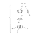
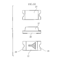
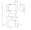
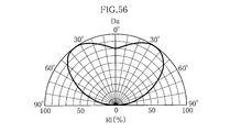
- the LED modules shown in FIGS. 20 to 58 may be respectively employed.
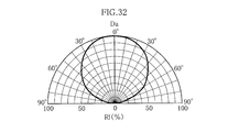
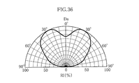
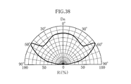
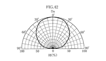
- the outline and directivity of each LED module are shown.
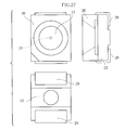
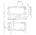
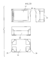
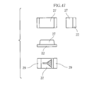
- the figure which shows the schematic external shape of an LED module it is a top view, a side view, and a bottom view from the top, and the right figure of the top view is a right side view.
- 20 to 32 show an LED module with a reflector that can be used as the first LED module 2A.
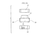
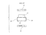
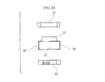
- 33 to 42 show a side light emitting LED module that can be used as the second LED module 2B.
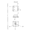
- FIGS. 43 to 58 show LED modules having a uniform light intensity distribution that can be adopted as the third LED module 2C.
- the LED modules shown in FIGS. 24 and 49 are two-color light emission types, and the LED modules shown in FIGS. 29, 39, and 57 are three-color light emission types.
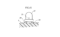
- a bullet-type LED module may be employed as shown in FIGS.
- the bullet-type LED module shown in FIG. 59 can be mounted in the vertical direction or the horizontal direction with respect to the support substrate 1. Therefore, depending on the mounting direction, the direction in which the relative luminous intensity ratio Rl is maximized can be arbitrarily matched with the direction matching the normal direction of the mounting surface of the support substrate 1 or the outside in the in-plane direction.
- the bullet type LED module shown in FIG. 61 has a simpler configuration than the bullet type LED module shown in FIG. It should be noted that a conventional LED module having two lead pins other than the bullet-type LED module shown in FIGS. 59 to 62 may be used.
- each lead pin penetrates the support substrate 1 or each lead pin is bent, for example, in the normal direction of the mounting surface of the support substrate 1 or within the mounting surface of the support substrate 1. It is also possible to have a directivity characteristic in which the luminous intensity distribution is biased in a direction coinciding with the outward direction.
Landscapes
- Engineering & Computer Science (AREA)
- Physics & Mathematics (AREA)
- Microelectronics & Electronic Packaging (AREA)
- Optics & Photonics (AREA)
- General Engineering & Computer Science (AREA)
- Non-Portable Lighting Devices Or Systems Thereof (AREA)
- Led Device Packages (AREA)
- Led Devices (AREA)
- Fastening Of Light Sources Or Lamp Holders (AREA)
Abstract
Description
図10に、第2LEDモジュール2Bの指向特性を示す。本図においては、指向角Da=0°の方向が、支持基板1の実装面1aの面内方向外方と一致している。第2LEDモジュール2Bは、指向角0°、すなわち実装面1aの面内方向外方に向かう相対光度比Rlが最大となっている。図1および図2に示すように、本実施形態においては、複数の第2LEDモジュール2Bが、支持基板1の幅方向の両端部に沿って複数個配置されている。
Claims (20)
- LEDチップをそれぞれ有する複数のLEDモジュールと、
上記複数のLEDモジュールが搭載された支持面を有する支持部材と、
を備えており、
上記複数のLEDモジュールは、出射方向についての光度分布である指向特性が互いに異なる複数種類のLEDモジュールによって構成されていることを特徴とする、LEDランプ。 - 上記複数のLEDモジュールは、上記支持面の中央寄りに位置する第1LEDモジュールを含んでおり、
上記第1LEDモジュールは、これ以外の上記LEDモジュールよりも、上記支持面の法線方向に光度分布が偏った指向特性を有する、請求項1に記載のLEDランプ。 - 上記第1LEDモジュールは、上記LEDチップを囲み、かつ上記法線方向に開口するリフレクタを備える、請求項2に記載のLEDランプ。
- 上記第1LEDモジュールは、上記LEDチップを封止する封止樹脂をさらに備えており、かつ、
上記封止樹脂は、上記リフレクタによって囲まれた空間に充填されている、請求項3に記載のLEDランプ。 - 上記第1LEDモジュールは、上記支持部材の上記支持面の法線方向における寸法が、上記支持面の面内方向における寸法よりも小である、請求項4に記載のLEDランプ。
- 上記第1LEDモジュールは、上記LEDチップが搭載された基板を備えており、
上記基板のうち上記LEDチップが搭載された面とは反対側の面には、実装端子が設けられている、請求項5に記載のLEDランプ。 - 上記複数のLEDモジュールは、上記支持面の端部寄りに位置する第2LEDモジュールを含んでおり、
上記第2LEDモジュールは、これ以外の上記LEDモジュールよりも、上記支持面の面内方向外方に光度分布が偏った指向特性を有する、請求項2に記載のLEDランプ。 - 上記第2LEDモジュールは、上記LEDチップを囲み、かつ上記面内方向外方に開口するリフレクタを備える、請求項7に記載のLEDランプ。
- 上記第2LEDモジュールは、上記LEDチップを封止する封止樹脂をさらに備えており、かつ、
上記封止樹脂は、上記リフレクタによって囲まれた空間に充填されている、請求項8に記載のLEDランプ。 - 上記第2LEDモジュールは、上記LEDチップが搭載された基板を備えており、かつ、上記基板の側面と上記支持部材の上記支持面とが対向する姿勢で上記支持部材に搭載されている、請求項9に記載のLEDランプ。
- 上記第2LEDモジュールは、上記支持部材の法線方向における寸法よりも上記支持部材の面内方向における寸法の方が大である、請求項10に記載のLEDランプ。
- 上記複数のLEDモジュールは、上記第1および第2LEDモジュールの間に位置し、かつ上記第1および第2LEDモジュールよりも出射方向についての光度分布が均一である指向特性を有する第3LEDモジュールをさらに含む、請求項7に記載のLEDランプ。
- 上記第3LEDモジュールは、上記LEDチップが搭載された基板を備えており、
上記基板のうち上記LEDチップが搭載された面とは反対側の面には、実装端子が設けられている、請求項12に記載のLEDランプ。 - 上記第3LEDモジュールは、上記LEDチップを封止する封止樹脂を備えており、
上記封止樹脂は、上記支持面の法線方向および面内方向のそれぞれにおいて露出している、請求項13に記載のLEDランプ。 - 上記支持面は、帯状であり、
複数の上記第1LEDモジュールが、上記支持面の中心寄りに長手方向に沿って配列されており、
複数の上記第2LEDモジュールが、上記支持面の幅方向両端に沿って配列されており、
複数の上記第3LEDモジュールが、上記複数の第1および第2LEDモジュールに挟まれた領域に長手方向に沿って配列されている、請求項12に記載のLEDランプ。 - 上記第1ないし第3LEDモジュールおよび上記支持部材を収容し、かつ、上記第1ないし第3LEDモジュールからの光を拡散させつつ透過させるケースをさらに備えている、請求項15に記載のLEDランプ。
- 上記ケースは、円筒形状である、請求項16に記載のLEDランプ。
- 上記支持部材は、絶縁基板であり、
上記絶縁基板のうち、上記支持面とは反対側の部分に接合された放熱部材をさらに備える、請求項17に記載のLEDランプ。 - 上記ケースには、内方に突出し、かつ上記基板を支持する突出片が形成されている、請求項18に記載のLEDランプ。
- 上記突出片は、上記放熱部材と係合している、請求項19に記載のLEDランプ。
Priority Applications (9)
| Application Number | Priority Date | Filing Date | Title |
|---|---|---|---|
| CN201080008938.8A CN102333987B (zh) | 2009-02-25 | 2010-02-24 | Led灯 |
| US13/202,910 US9234632B2 (en) | 2009-02-25 | 2010-02-24 | LED lamp |
| US14/968,100 US9797554B2 (en) | 2009-02-25 | 2015-12-14 | LED lamp |
| US15/707,759 US10190729B2 (en) | 2009-02-25 | 2017-09-18 | LED lamp |
| US16/242,090 US20190137049A1 (en) | 2009-02-25 | 2019-01-08 | Led lamp |
| US17/008,007 US11629826B2 (en) | 2009-02-25 | 2020-08-31 | LED lamp |
| US17/191,307 US20210190274A1 (en) | 2009-02-25 | 2021-03-03 | Led lamp |
| US17/235,784 US11608941B2 (en) | 2009-02-25 | 2021-04-20 | LED lamp |
| US18/166,374 US12392458B2 (en) | 2009-02-25 | 2023-02-08 | LED lamp |
Applications Claiming Priority (2)
| Application Number | Priority Date | Filing Date | Title |
|---|---|---|---|
| JP2009042543A JP5340763B2 (ja) | 2009-02-25 | 2009-02-25 | Ledランプ |
| JP2009-042543 | 2009-02-25 |
Related Child Applications (2)
| Application Number | Title | Priority Date | Filing Date |
|---|---|---|---|
| US13/202,910 A-371-Of-International US9234632B2 (en) | 2009-02-25 | 2010-02-24 | LED lamp |
| US14/968,100 Continuation US9797554B2 (en) | 2009-02-25 | 2015-12-14 | LED lamp |
Publications (1)
| Publication Number | Publication Date |
|---|---|
| WO2010098349A1 true WO2010098349A1 (ja) | 2010-09-02 |
Family
ID=42665555
Family Applications (1)
| Application Number | Title | Priority Date | Filing Date |
|---|---|---|---|
| PCT/JP2010/052870 Ceased WO2010098349A1 (ja) | 2009-02-25 | 2010-02-24 | Ledランプ |
Country Status (4)
| Country | Link |
|---|---|
| US (8) | US9234632B2 (ja) |
| JP (1) | JP5340763B2 (ja) |
| CN (1) | CN102333987B (ja) |
| WO (1) | WO2010098349A1 (ja) |
Cited By (2)
| Publication number | Priority date | Publication date | Assignee | Title |
|---|---|---|---|---|
| JP2012069303A (ja) * | 2010-09-21 | 2012-04-05 | Panasonic Corp | ランプ及び照明装置 |
| WO2013176000A1 (ja) * | 2012-05-23 | 2013-11-28 | 船井電機株式会社 | 照明装置 |
Families Citing this family (22)
| Publication number | Priority date | Publication date | Assignee | Title |
|---|---|---|---|---|
| US11480306B2 (en) | 2008-09-05 | 2022-10-25 | Jiaxing Super Lighting Electric Appliance Co., Ltd. | LED tube lamp |
| US11131431B2 (en) | 2014-09-28 | 2021-09-28 | Jiaxing Super Lighting Electric Appliance Co., Ltd | LED tube lamp |
| JP5669092B2 (ja) * | 2011-01-24 | 2015-02-12 | パナソニックIpマネジメント株式会社 | Ledユニットおよび照明器具 |
| WO2013132383A1 (en) * | 2012-03-05 | 2013-09-12 | Koninklijke Philips N.V. | Lighting device |
| SE536603C2 (sv) * | 2012-03-15 | 2014-03-25 | Auralight Int Ab | LED-lysrör |
| JP2014143125A (ja) * | 2013-01-25 | 2014-08-07 | Stanley Electric Co Ltd | 両面発光ledランプ |
| WO2014206759A1 (en) | 2013-06-25 | 2014-12-31 | Koninklijke Philips N.V. | Lighting device, luminaire and lighting device assembly method |
| KR20160071414A (ko) * | 2013-10-17 | 2016-06-21 | 가부시끼가이샤 사따께 | 색채 선별기용의 조명 장치 |
| CN105333393A (zh) * | 2014-08-13 | 2016-02-17 | 欧司朗有限公司 | 照明装置 |
| US11480305B2 (en) | 2014-09-25 | 2022-10-25 | Jiaxing Super Lighting Electric Appliance Co., Ltd. | LED tube lamp |
| US10560989B2 (en) | 2014-09-28 | 2020-02-11 | Jiaxing Super Lighting Electric Appliance Co., Ltd | LED tube lamp |
| CN115095808A (zh) | 2014-09-28 | 2022-09-23 | 嘉兴山蒲照明电器有限公司 | 一种led直管灯 |
| US9989200B2 (en) | 2014-10-20 | 2018-06-05 | Argo Import-Export Ltd. | LED lighting tube device and method |
| US9810384B2 (en) * | 2014-10-20 | 2017-11-07 | Argo Import-Export Ltd | LED lighting tube device and method |
| US12264789B2 (en) | 2014-12-05 | 2025-04-01 | Jiaxing Super Lighting Electric Appliance Co., Ltd | LED tube lamp |
| US10514134B2 (en) | 2014-12-05 | 2019-12-24 | Jiaxing Super Lighting Electric Appliance Co., Ltd | LED tube lamp |
| US9897265B2 (en) | 2015-03-10 | 2018-02-20 | Jiaxing Super Lighting Electric Appliance Co., Ltd. | LED tube lamp having LED light strip |
| DE102015205030A1 (de) * | 2015-03-19 | 2016-09-22 | Osram Gmbh | Halbleiterlampe |
| JP6662322B2 (ja) * | 2017-02-09 | 2020-03-11 | 日亜化学工業株式会社 | 発光装置 |
| JP6699580B2 (ja) * | 2017-02-09 | 2020-05-27 | 日亜化学工業株式会社 | 発光装置 |
| CN220911411U (zh) | 2023-07-28 | 2024-05-07 | 深圳市凯思瑞科技有限公司 | 一种带计时器的挂脖led灯 |
| US20250160069A1 (en) * | 2023-11-14 | 2025-05-15 | Guangxi Xinyi Phoyoelectric Technology Co.,Ltd | Fully luminous led light source |
Citations (10)
| Publication number | Priority date | Publication date | Assignee | Title |
|---|---|---|---|---|
| JPS6395261U (ja) * | 1986-12-11 | 1988-06-20 | ||
| JPH0492660U (ja) * | 1990-12-28 | 1992-08-12 | ||
| JPH1117228A (ja) * | 1997-06-20 | 1999-01-22 | Ushio Inc | 照明灯 |
| JPH11306811A (ja) * | 1998-04-27 | 1999-11-05 | Stanley Electric Co Ltd | 車両用信号灯具 |
| JP2002197901A (ja) * | 2000-12-25 | 2002-07-12 | Matsushita Electric Works Ltd | Led照明器具 |
| JP2004109407A (ja) * | 2002-09-18 | 2004-04-08 | Joi T:Kk | ディスプレイ管及びディスプレイシステム |
| JP2005159263A (ja) * | 2003-10-30 | 2005-06-16 | Kyocera Corp | 発光装置および照明装置 |
| JP3145640U (ja) * | 2008-08-01 | 2008-10-16 | 佐野 明宏 | 発光装置 |
| JP2008258094A (ja) * | 2007-04-09 | 2008-10-23 | M & S Fine Tec Kk | Ledバックライトおよび液晶表示装置 |
| JP3148527U (ja) * | 2008-11-10 | 2009-02-19 | 珍通能源技術股▲ふん▼有限公司 | 回路板位置を多段調整可能な発光ダイオード灯管 |
Family Cites Families (81)
| Publication number | Priority date | Publication date | Assignee | Title |
|---|---|---|---|---|
| JP4482193B2 (ja) * | 2000-03-31 | 2010-06-16 | パナソニック電工株式会社 | 同軸コネクタ用レセプタクル |
| JPS6395261A (ja) | 1986-10-09 | 1988-04-26 | Mitsubishi Monsanto Chem Co | ガラス繊維強化アミド系樹脂成形品用ガラス繊維 |
| JPH0492660A (ja) | 1990-08-08 | 1992-03-25 | Masayoshi Kishigami | 人工股関節の爪つきソケット |
| JPH0654103U (ja) | 1992-03-06 | 1994-07-22 | 高立株式会社 | 蛍光灯型led投光器 |
| JP3148527B2 (ja) | 1994-07-22 | 2001-03-19 | 松下電工株式会社 | モータ駆動気泡ジェットバスとそのモータ駆動装置 |
| DE19549818B4 (de) * | 1995-09-29 | 2010-03-18 | Osram Opto Semiconductors Gmbh | Optoelektronisches Halbleiter-Bauelement |
| JP3145640B2 (ja) | 1996-08-16 | 2001-03-12 | 日本無線株式会社 | スイッチング電力増幅器 |
| TW330233B (en) * | 1997-01-23 | 1998-04-21 | Philips Eloctronics N V | Luminary |
| JP3707024B2 (ja) * | 1997-04-17 | 2005-10-19 | 松下電器産業株式会社 | 電子部品 |
| WO1999007023A1 (de) * | 1997-07-29 | 1999-02-11 | Osram Opto Semiconductors Gmbh & Co. Ohg | Optoelektronisches bauelement |
| US7049761B2 (en) * | 2000-02-11 | 2006-05-23 | Altair Engineering, Inc. | Light tube and power supply circuit |
| JP2001244416A (ja) * | 2000-02-29 | 2001-09-07 | Hitachi Ltd | 信号処理用半導体集積回路 |
| US20020123163A1 (en) * | 2000-04-24 | 2002-09-05 | Takehiro Fujii | Edge-emitting light-emitting semiconductor device and method of manufacture thereof |
| JP3685018B2 (ja) * | 2000-05-09 | 2005-08-17 | 日亜化学工業株式会社 | 発光素子とその製造方法 |
| MY145695A (en) * | 2001-01-24 | 2012-03-30 | Nichia Corp | Light emitting diode, optical semiconductor device, epoxy resin composition suited for optical semiconductor device, and method for manufacturing the same |
| JP2002314143A (ja) * | 2001-04-09 | 2002-10-25 | Toshiba Corp | 発光装置 |
| JP2003051618A (ja) * | 2001-08-06 | 2003-02-21 | Rohm Co Ltd | チップ型半導体発光装置 |
| US7242033B2 (en) * | 2002-03-08 | 2007-07-10 | Rohm Co., Ltd. | Semiconductor device using LED chip |
| US7244965B2 (en) * | 2002-09-04 | 2007-07-17 | Cree Inc, | Power surface mount light emitting die package |
| DE10255932A1 (de) * | 2002-11-29 | 2004-06-17 | Osram Opto Semiconductors Gmbh | Optoelektronisches Bauelement |
| JP4504662B2 (ja) * | 2003-04-09 | 2010-07-14 | シチズン電子株式会社 | Ledランプ |
| US20050133808A1 (en) | 2003-09-11 | 2005-06-23 | Kyocera Corporation | Package for housing light-emitting element, light-emitting apparatus and illumination apparatus |
| TWI275189B (en) * | 2003-12-30 | 2007-03-01 | Osram Opto Semiconductors Gmbh | Radiation-emitting and/or radiation-receiving semiconductor component and method for producing such component |
| IES20050086A2 (en) * | 2004-02-17 | 2005-09-21 | William M Kelly | A utility lamp |
| US20080186714A1 (en) * | 2004-03-25 | 2008-08-07 | Citizen Electronics Co., Ltd. | Light-emitting diode |
| US7509043B2 (en) * | 2004-05-25 | 2009-03-24 | Nikon Corporation | Illuminating device for photographing and camera |
| EP1816685A4 (en) * | 2004-10-27 | 2010-01-13 | Kyocera Corp | LIGHT EMITTING ELEMENT PLATE, BEARING CAPACITOR FOR LIGHT EMITTING ELEMENTS, LIGHT EMITTING DEVICE AND LIGHTING DEVICE |
| JP4623282B2 (ja) * | 2005-03-10 | 2011-02-02 | 信越化学工業株式会社 | 半導体装置の製造方法 |
| US7455431B2 (en) * | 2005-03-11 | 2008-11-25 | Richard Brower | High efficiency light fixture |
| JP2006261540A (ja) * | 2005-03-18 | 2006-09-28 | Stanley Electric Co Ltd | 発光デバイス |
| JP2006310771A (ja) * | 2005-03-30 | 2006-11-09 | Toshiba Discrete Technology Kk | 半導体発光装置 |
| JP2007042901A (ja) * | 2005-08-04 | 2007-02-15 | Rohm Co Ltd | 発光モジュールおよび発光ユニット |
| US7284871B2 (en) * | 2005-08-08 | 2007-10-23 | Avago Technologies Ecb4 Ip (Singapore) Pte Ltd | Light-emitting diode module for flash and auto-focus application |
| US7311423B2 (en) * | 2005-09-21 | 2007-12-25 | Awi Licensing Company | Adjustable LED luminaire |
| CN101268120B (zh) * | 2005-09-22 | 2011-09-14 | 三菱化学株式会社 | 半导体发光器件用部件及其制造方法、以及使用该部件的半导体发光器件 |
| JP2007194385A (ja) * | 2006-01-19 | 2007-08-02 | Stanley Electric Co Ltd | 半導体発光装置及び半導体発光装置の製造方法 |
| JP2009528556A (ja) * | 2006-02-27 | 2009-08-06 | イルミネーション マネジメント ソリューションズ インコーポレイテッド | 幅広ビーム生成のための改良ledデバイス |
| US7635915B2 (en) * | 2006-04-26 | 2009-12-22 | Cree Hong Kong Limited | Apparatus and method for use in mounting electronic elements |
| JP4863203B2 (ja) * | 2006-04-28 | 2012-01-25 | スタンレー電気株式会社 | 半導体発光装置 |
| US7665862B2 (en) * | 2006-09-12 | 2010-02-23 | Cree, Inc. | LED lighting fixture |
| US8905579B2 (en) * | 2006-10-24 | 2014-12-09 | Ellenby Technologies, Inc. | Vending machine having LED lamp with control and communication circuits |
| JP2008123973A (ja) * | 2006-11-16 | 2008-05-29 | Mitsubishi Electric Corp | 面状光源装置および液晶表示装置 |
| JP5179766B2 (ja) * | 2007-03-08 | 2013-04-10 | スタンレー電気株式会社 | 半導体発光装置およびその製造方法 |
| KR100898818B1 (ko) * | 2007-03-30 | 2009-05-22 | 한국광기술원 | 배광 제어가 가능한 발광다이오드 전구 |
| JP5122172B2 (ja) * | 2007-03-30 | 2013-01-16 | ローム株式会社 | 半導体発光装置 |
| US7964888B2 (en) * | 2007-04-18 | 2011-06-21 | Cree, Inc. | Semiconductor light emitting device packages and methods |
| US7923831B2 (en) * | 2007-05-31 | 2011-04-12 | Avago Technologies Ecbu Ip (Singapore) Pte. Ltd. | LED-based light source having improved thermal dissipation |
| CN101388161A (zh) * | 2007-09-14 | 2009-03-18 | 科锐香港有限公司 | Led表面安装装置和并入有此装置的led显示器 |
| CN201081165Y (zh) | 2007-09-14 | 2008-07-02 | 鹤山丽得电子实业有限公司 | 一种led日光灯管 |
| DE102007054206A1 (de) * | 2007-10-15 | 2009-04-16 | Harald Hofmann | LED-Lampe mit Diffusor |
| KR100924911B1 (ko) * | 2007-11-01 | 2009-11-03 | 서울반도체 주식회사 | Led 조명장치 |
| JP5340583B2 (ja) * | 2007-11-26 | 2013-11-13 | スタンレー電気株式会社 | 半導体発光装置 |
| US20090140271A1 (en) * | 2007-11-30 | 2009-06-04 | Wen-Jyh Sah | Light emitting unit |
| CN101884257B (zh) * | 2007-12-05 | 2012-02-08 | 三菱树脂株式会社 | 具有腔部的多层布线基板 |
| JP5182927B2 (ja) * | 2008-04-01 | 2013-04-17 | 日亜化学工業株式会社 | 照明装置 |
| KR101002464B1 (ko) * | 2008-05-15 | 2010-12-17 | 엄기인 | 옥외용 발광다이오드 조명등 |
| US8356916B2 (en) * | 2008-05-16 | 2013-01-22 | Musco Corporation | Method, system and apparatus for highly controlled light distribution from light fixture using multiple light sources (LEDS) |
| JP2011521422A (ja) * | 2008-05-22 | 2011-07-21 | パク,ホビョン | Led照明装置 |
| US8360599B2 (en) * | 2008-05-23 | 2013-01-29 | Ilumisys, Inc. | Electric shock resistant L.E.D. based light |
| KR100866586B1 (ko) * | 2008-07-29 | 2008-11-03 | 엔 하이테크 주식회사 | 엘이디를 이용한 형광등 |
| US8901823B2 (en) * | 2008-10-24 | 2014-12-02 | Ilumisys, Inc. | Light and light sensor |
| US8029159B2 (en) * | 2008-10-27 | 2011-10-04 | Edison Opto Corporation | Light source device having different color temperature rotating lighting modules |
| US8853712B2 (en) * | 2008-11-18 | 2014-10-07 | Cree, Inc. | High efficacy semiconductor light emitting devices employing remote phosphor configurations |
| US8748905B2 (en) * | 2008-11-18 | 2014-06-10 | Cree, Inc. | High efficacy semiconductor light emitting devices employing remote phosphor configurations |
| US10431567B2 (en) * | 2010-11-03 | 2019-10-01 | Cree, Inc. | White ceramic LED package |
| US8368112B2 (en) * | 2009-01-14 | 2013-02-05 | Cree Huizhou Opto Limited | Aligned multiple emitter package |
| US7997770B1 (en) * | 2009-02-12 | 2011-08-16 | William Henry Meurer | LED tube reusable end cap |
| US20120033420A1 (en) * | 2009-04-08 | 2012-02-09 | Sun Woong Kim | Led lamp having broad and uniform light distribution |
| CN101886753A (zh) * | 2009-05-11 | 2010-11-17 | 富准精密工业(深圳)有限公司 | 发光二极管灯具 |
| TW201128812A (en) | 2009-12-01 | 2011-08-16 | Lg Innotek Co Ltd | Light emitting device |
| JP5356273B2 (ja) * | 2010-02-05 | 2013-12-04 | シャープ株式会社 | 照明デバイスおよび該照明デバイスを備えた照明装置 |
| US20110255276A1 (en) * | 2010-04-19 | 2011-10-20 | Coward Mark T | Lighting assembly |
| US20110303936A1 (en) * | 2010-06-10 | 2011-12-15 | Shang-Yi Wu | Light emitting device package structure and fabricating method thereof |
| US8330362B2 (en) * | 2010-07-22 | 2012-12-11 | Chiu-Min Lin | Lamp having mounting slot |
| US8501509B2 (en) * | 2010-08-25 | 2013-08-06 | Micron Technology, Inc. | Multi-dimensional solid state lighting device array system and associated methods and structures |
| DE102010062331B4 (de) * | 2010-12-02 | 2012-07-05 | Osram Ag | Herstellungsverfahren für eine LED-Lampe und eine entsprechende LED-Lampe |
| US20130135853A1 (en) * | 2011-11-29 | 2013-05-30 | Chi-Feng Lin | Light-guiding element, light-emitting diode lamp tube and illumination lamp |
| US20140151731A1 (en) * | 2012-06-15 | 2014-06-05 | Nguyen The Tran | Photon conversion structures, devices for light emitting devices |
| JP6209874B2 (ja) * | 2012-08-31 | 2017-10-11 | 日亜化学工業株式会社 | 発光装置及びその製造方法 |
| US9123685B2 (en) * | 2013-07-15 | 2015-09-01 | Freescale Semiconductor Inc. | Microelectronic packages having frontside thermal contacts and methods for the fabrication thereof |
| WO2016117910A1 (ko) * | 2015-01-19 | 2016-07-28 | 엘지이노텍 주식회사 | 발광 소자 |
-
2009
- 2009-02-25 JP JP2009042543A patent/JP5340763B2/ja not_active Expired - Fee Related
-
2010
- 2010-02-24 CN CN201080008938.8A patent/CN102333987B/zh active Active
- 2010-02-24 US US13/202,910 patent/US9234632B2/en active Active
- 2010-02-24 WO PCT/JP2010/052870 patent/WO2010098349A1/ja not_active Ceased
-
2015
- 2015-12-14 US US14/968,100 patent/US9797554B2/en not_active Expired - Fee Related
-
2017
- 2017-09-18 US US15/707,759 patent/US10190729B2/en active Active
-
2019
- 2019-01-08 US US16/242,090 patent/US20190137049A1/en not_active Abandoned
-
2020
- 2020-08-31 US US17/008,007 patent/US11629826B2/en active Active
-
2021
- 2021-03-03 US US17/191,307 patent/US20210190274A1/en not_active Abandoned
- 2021-04-20 US US17/235,784 patent/US11608941B2/en active Active
-
2023
- 2023-02-08 US US18/166,374 patent/US12392458B2/en active Active
Patent Citations (10)
| Publication number | Priority date | Publication date | Assignee | Title |
|---|---|---|---|---|
| JPS6395261U (ja) * | 1986-12-11 | 1988-06-20 | ||
| JPH0492660U (ja) * | 1990-12-28 | 1992-08-12 | ||
| JPH1117228A (ja) * | 1997-06-20 | 1999-01-22 | Ushio Inc | 照明灯 |
| JPH11306811A (ja) * | 1998-04-27 | 1999-11-05 | Stanley Electric Co Ltd | 車両用信号灯具 |
| JP2002197901A (ja) * | 2000-12-25 | 2002-07-12 | Matsushita Electric Works Ltd | Led照明器具 |
| JP2004109407A (ja) * | 2002-09-18 | 2004-04-08 | Joi T:Kk | ディスプレイ管及びディスプレイシステム |
| JP2005159263A (ja) * | 2003-10-30 | 2005-06-16 | Kyocera Corp | 発光装置および照明装置 |
| JP2008258094A (ja) * | 2007-04-09 | 2008-10-23 | M & S Fine Tec Kk | Ledバックライトおよび液晶表示装置 |
| JP3145640U (ja) * | 2008-08-01 | 2008-10-16 | 佐野 明宏 | 発光装置 |
| JP3148527U (ja) * | 2008-11-10 | 2009-02-19 | 珍通能源技術股▲ふん▼有限公司 | 回路板位置を多段調整可能な発光ダイオード灯管 |
Cited By (2)
| Publication number | Priority date | Publication date | Assignee | Title |
|---|---|---|---|---|
| JP2012069303A (ja) * | 2010-09-21 | 2012-04-05 | Panasonic Corp | ランプ及び照明装置 |
| WO2013176000A1 (ja) * | 2012-05-23 | 2013-11-28 | 船井電機株式会社 | 照明装置 |
Also Published As
| Publication number | Publication date |
|---|---|
| US20110303928A1 (en) | 2011-12-15 |
| US20160097491A1 (en) | 2016-04-07 |
| JP5340763B2 (ja) | 2013-11-13 |
| US11608941B2 (en) | 2023-03-21 |
| US9797554B2 (en) | 2017-10-24 |
| JP2010198919A (ja) | 2010-09-09 |
| US10190729B2 (en) | 2019-01-29 |
| US20200393089A1 (en) | 2020-12-17 |
| US20180003347A1 (en) | 2018-01-04 |
| CN102333987B (zh) | 2014-10-08 |
| US11629826B2 (en) | 2023-04-18 |
| US20210239279A1 (en) | 2021-08-05 |
| US20230184394A1 (en) | 2023-06-15 |
| CN102333987A (zh) | 2012-01-25 |
| US12392458B2 (en) | 2025-08-19 |
| US20210190274A1 (en) | 2021-06-24 |
| US9234632B2 (en) | 2016-01-12 |
| US20190137049A1 (en) | 2019-05-09 |
Similar Documents
| Publication | Publication Date | Title |
|---|---|---|
| US12392458B2 (en) | LED lamp | |
| JP4124479B1 (ja) | 照明装置 | |
| US9885457B2 (en) | LED illumination lamp bulb with internal reflector | |
| KR101253199B1 (ko) | 조명 장치 | |
| US8931929B2 (en) | Light emitting diode primary optic for beam shaping | |
| WO2010082655A1 (ja) | Ledランプ | |
| KR101349843B1 (ko) | 조명 장치 | |
| CN102933898A (zh) | 照明装置 | |
| JPWO2014091655A1 (ja) | 発光装置、照明用光源及び照明装置 | |
| JP5286048B2 (ja) | Ledランプ | |
| JP2014179331A (ja) | 照明用光源及び照明装置 | |
| JP3163443U (ja) | Led式照明装置 | |
| JP2009272263A (ja) | Ledランプ | |
| JP5540157B2 (ja) | ランプ及び照明装置 | |
| KR101221279B1 (ko) | 엘이디 램프 | |
| TWI613394B (zh) | 車燈模組 | |
| TW201513414A (zh) | 發光模組及照明裝置 | |
| KR20120126891A (ko) | 엘이디 벌브 | |
| WO2013046292A1 (ja) | 発光モジュール、および照明器具 | |
| KR20150032766A (ko) | 발광 모듈 및 조명 장치 |
Legal Events
| Date | Code | Title | Description |
|---|---|---|---|
| WWE | Wipo information: entry into national phase |
Ref document number: 201080008938.8 Country of ref document: CN |
|
| 121 | Ep: the epo has been informed by wipo that ep was designated in this application |
Ref document number: 10746229 Country of ref document: EP Kind code of ref document: A1 |
|
| WWE | Wipo information: entry into national phase |
Ref document number: 13202910 Country of ref document: US |
|
| NENP | Non-entry into the national phase |
Ref country code: DE |
|
| 122 | Ep: pct application non-entry in european phase |
Ref document number: 10746229 Country of ref document: EP Kind code of ref document: A1 |