WO2010073520A1 - 固体撮像デバイスおよびその製造方法 - Google Patents
固体撮像デバイスおよびその製造方法 Download PDFInfo
- Publication number
- WO2010073520A1 WO2010073520A1 PCT/JP2009/006773 JP2009006773W WO2010073520A1 WO 2010073520 A1 WO2010073520 A1 WO 2010073520A1 JP 2009006773 W JP2009006773 W JP 2009006773W WO 2010073520 A1 WO2010073520 A1 WO 2010073520A1
- Authority
- WO
- WIPO (PCT)
- Prior art keywords
- solid
- state imaging
- imaging device
- signal processing
- image sensor
- Prior art date
- Legal status (The legal status is an assumption and is not a legal conclusion. Google has not performed a legal analysis and makes no representation as to the accuracy of the status listed.)
- Ceased
Links
Images





Classifications
-
- H—ELECTRICITY
- H04—ELECTRIC COMMUNICATION TECHNIQUE
- H04N—PICTORIAL COMMUNICATION, e.g. TELEVISION
- H04N25/00—Circuitry of solid-state image sensors [SSIS]; Control thereof
- H04N25/70—SSIS architectures; Circuits associated therewith
- H04N25/71—Charge-coupled device [CCD] sensors; Charge-transfer registers specially adapted for CCD sensors
- H04N25/75—Circuitry for providing, modifying or processing image signals from the pixel array
-
- H—ELECTRICITY
- H04—ELECTRIC COMMUNICATION TECHNIQUE
- H04N—PICTORIAL COMMUNICATION, e.g. TELEVISION
- H04N25/00—Circuitry of solid-state image sensors [SSIS]; Control thereof
- H04N25/70—SSIS architectures; Circuits associated therewith
- H04N25/76—Addressed sensors, e.g. MOS or CMOS sensors
-
- H—ELECTRICITY
- H10—SEMICONDUCTOR DEVICES; ELECTRIC SOLID-STATE DEVICES NOT OTHERWISE PROVIDED FOR
- H10F—INORGANIC SEMICONDUCTOR DEVICES SENSITIVE TO INFRARED RADIATION, LIGHT, ELECTROMAGNETIC RADIATION OF SHORTER WAVELENGTH OR CORPUSCULAR RADIATION
- H10F39/00—Integrated devices, or assemblies of multiple devices, comprising at least one element covered by group H10F30/00, e.g. radiation detectors comprising photodiode arrays
- H10F39/011—Manufacture or treatment of image sensors covered by group H10F39/12
-
- H—ELECTRICITY
- H10—SEMICONDUCTOR DEVICES; ELECTRIC SOLID-STATE DEVICES NOT OTHERWISE PROVIDED FOR
- H10F—INORGANIC SEMICONDUCTOR DEVICES SENSITIVE TO INFRARED RADIATION, LIGHT, ELECTROMAGNETIC RADIATION OF SHORTER WAVELENGTH OR CORPUSCULAR RADIATION
- H10F39/00—Integrated devices, or assemblies of multiple devices, comprising at least one element covered by group H10F30/00, e.g. radiation detectors comprising photodiode arrays
- H10F39/80—Constructional details of image sensors
- H10F39/809—Constructional details of image sensors of hybrid image sensors
-
- H—ELECTRICITY
- H10—SEMICONDUCTOR DEVICES; ELECTRIC SOLID-STATE DEVICES NOT OTHERWISE PROVIDED FOR
- H10W—GENERIC PACKAGES, INTERCONNECTIONS, CONNECTORS OR OTHER CONSTRUCTIONAL DETAILS OF DEVICES COVERED BY CLASS H10
- H10W72/00—Interconnections or connectors in packages
- H10W72/20—Bump connectors, e.g. solder bumps or copper pillars; Dummy bumps; Thermal bumps
-
- H—ELECTRICITY
- H10—SEMICONDUCTOR DEVICES; ELECTRIC SOLID-STATE DEVICES NOT OTHERWISE PROVIDED FOR
- H10F—INORGANIC SEMICONDUCTOR DEVICES SENSITIVE TO INFRARED RADIATION, LIGHT, ELECTROMAGNETIC RADIATION OF SHORTER WAVELENGTH OR CORPUSCULAR RADIATION
- H10F39/00—Integrated devices, or assemblies of multiple devices, comprising at least one element covered by group H10F30/00, e.g. radiation detectors comprising photodiode arrays
- H10F39/10—Integrated devices
- H10F39/12—Image sensors
- H10F39/15—Charge-coupled device [CCD] image sensors
-
- H—ELECTRICITY
- H10—SEMICONDUCTOR DEVICES; ELECTRIC SOLID-STATE DEVICES NOT OTHERWISE PROVIDED FOR
- H10W—GENERIC PACKAGES, INTERCONNECTIONS, CONNECTORS OR OTHER CONSTRUCTIONAL DETAILS OF DEVICES COVERED BY CLASS H10
- H10W72/00—Interconnections or connectors in packages
- H10W72/90—Bond pads, in general
- H10W72/941—Dispositions of bond pads
- H10W72/944—Dispositions of multiple bond pads
- H10W72/9445—Top-view layouts, e.g. mirror arrays
-
- H—ELECTRICITY
- H10—SEMICONDUCTOR DEVICES; ELECTRIC SOLID-STATE DEVICES NOT OTHERWISE PROVIDED FOR
- H10W—GENERIC PACKAGES, INTERCONNECTIONS, CONNECTORS OR OTHER CONSTRUCTIONAL DETAILS OF DEVICES COVERED BY CLASS H10
- H10W74/00—Encapsulations, e.g. protective coatings
- H10W74/10—Encapsulations, e.g. protective coatings characterised by their shape or disposition
- H10W74/15—Encapsulations, e.g. protective coatings characterised by their shape or disposition on active surfaces of flip-chip devices, e.g. underfills
-
- Y—GENERAL TAGGING OF NEW TECHNOLOGICAL DEVELOPMENTS; GENERAL TAGGING OF CROSS-SECTIONAL TECHNOLOGIES SPANNING OVER SEVERAL SECTIONS OF THE IPC; TECHNICAL SUBJECTS COVERED BY FORMER USPC CROSS-REFERENCE ART COLLECTIONS [XRACs] AND DIGESTS
- Y10—TECHNICAL SUBJECTS COVERED BY FORMER USPC
- Y10T—TECHNICAL SUBJECTS COVERED BY FORMER US CLASSIFICATION
- Y10T29/00—Metal working
- Y10T29/49—Method of mechanical manufacture
- Y10T29/49002—Electrical device making
- Y10T29/49117—Conductor or circuit manufacturing
- Y10T29/49124—On flat or curved insulated base, e.g., printed circuit, etc.
- Y10T29/49128—Assembling formed circuit to base
Definitions
- the present invention relates to a small-sized and low-cost solid-state imaging device and a manufacturing method thereof.
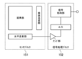
- the sensor block 151 and the signal processing block 152 are made of the same semiconductor.
- a solid-state imaging device configured in a substrate has been reported. Based on this configuration, in order to achieve further miniaturization and higher speed, a form called SIP (System ⁇ in Package) in which a solid-state imaging device and a plurality of chips that are peripheral circuits are integrally mounted as a semiconductor module. It has been reported.
- SIP System ⁇ in Package
- Patent Document 2 a solid-state image sensor 112 and a peripheral circuit element 111 are stacked and mounted as shown in FIG. 11, and electrical connection between the solid-state image sensor 112 and the peripheral circuit element 111 is performed via the multilayer substrate 110.
- the structure is disclosed.
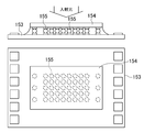
- CMOS image sensor chip 154 is stacked and mounted on a signal processing chip 153 with micro bumps 155, and signals are input and output from the signal processing chip 153.
- the structure is disclosed.
- Patent Document 4 discloses a configuration that realizes miniaturization by COC (Chip-on-Chip) technology in which main surfaces of different semiconductor elements are connected to face each other. ing.
- JP 2000-224495 A Japanese Patent Laid-Open No. 11-261044 (page 7, FIG. 1) JP 2006-49361 A JP 2004-146728 A (Page 9, FIG. 1)
- the peripheral circuit element 111 is flip-chip mounted on the multilayer substrate 110
- the solid-state image sensor 112 is mounted on the back surface of the peripheral circuit element 111
- the solid-state image sensor 112 and the multilayer substrate 110 are connected by wire bonding.
- the wiring density of the multilayer substrate becomes high, resulting in high costs, or the area of wire bonds of many input / output terminals. Therefore, there arises a problem that the size cannot be reduced so much.
- the area occupied by the wiring directly leads to an increase in the size of the solid-state imaging device.
- the signal processing circuit adopts 5 to 6 wiring layers used in a general system LSI
- the transistor coverage determined by the transistor layout and wiring is about 80%.
- the transistor coverage is reduced to about 30 to 40%. For this reason, the area of the signal processing circuit increases more than twice.
- the above-described problem of chip size increase is addressed by stacking and mounting the image sensor chip 154 on the signal processing chip 153.
- a back-illuminated image sensor having a light receiving surface different from the circuit surface is used as the image sensor chip 154. It has a complicated configuration of using.
- the signal processing chip 153 needs to receive a voltage generally used by the image sensor chip 154 having a high operating voltage.
- the solid-state image sensor is overlapped and pasted on the signal processing element, a through-wiring is passed through the substrate of the solid-state image sensor, and the lower signal processing element is electrically connected using a micro bump.
- connection There is an example of connection.
- a solid-state imaging device having a complicated configuration is required as in the configuration of FIG.
- the solid-state imaging device is overlaid on the signal processing device, the two devices are arranged on the circuit board, wire bonding is performed between each device and the circuit substrate, and the two devices are electrically connected by this wire bonding.
- connection There is an example of connection.
- the input / output terminals cannot be miniaturized and are not suitable for miniaturization, and are not suitable for high speed due to the impedance of the wire bond.
- the process of the system LSI has progressed, and the area of the signal processing circuit has been greatly reduced as compared with the solid-state imaging device in which the imaging region is uniquely determined by the optical size. For this reason, in actual devices, there is a reality that the chip size is determined by the number of input / output terminals of the signal processing element.
- an object of the present invention is to realize downsizing of a solid-state imaging device without affecting the imaging region by dust or stress.
- Another object of the present invention is to solve the above-mentioned conventional problems and realize further downsizing and cost reduction in a solid-state imaging device including a solid-state imaging element and a signal processing element.
- a solid-state imaging device having an imaging region on a main surface in which unit pixels including photoelectric conversion elements are formed in a matrix, and control of imaging operation of the solid-state imaging device or A peripheral circuit element that performs signal processing of video output of the solid-state imaging device, and the peripheral circuit element is in a region other than the imaging region on the main surface of the solid-state imaging device, the main surface of which is the solid-state imaging device
- the imaging area is covered with a transparent material and is mounted so as to face the main surface.
- the peripheral circuit element is mounted in a region other than the imaging region of the solid-state image sensor so that the main surfaces face each other, the electrical connection between the solid-state image sensor and the peripheral circuit element is achieved. For this reason, a laminated substrate and wire bonding are not required, so that the solid-state imaging device can be reduced in size and cost.
- recent advances in bump formation technology between solid-state image sensors and peripheral circuit elements enable connection of a large number of input / output terminals, enabling data transfer to be performed in parallel, resulting in high speed and low consumption. Electricity can be realized.
- the imaging area of the solid-state imaging device is covered with a transparent material, it is possible to avoid the influence of dust on the imaging area when mounting, and the stress applied to the imaging area is also reduced by this transparent material. It becomes possible.
- the transparent material is bonded to the surface of the imaging region with an adhesive. As a result, it is possible to more effectively relieve the stress applied to the imaging region during mounting.
- the solid-state imaging element is formed on the back surface and the through electrode that electrically connects the main surface and the back surface, and is electrically connected to the through electrode. It is preferable to provide a connection terminal. As a result, electrical connection is realized simply by attaching the back surface of the solid-state imaging device to the substrate. Therefore, when the solid-state imaging device is mounted on, for example, a camera, the mounting cost and mounting volume can be reduced. It becomes possible.
- a solid-state imaging device having an imaging region on a main surface in which unit pixels including photoelectric conversion elements are two-dimensionally arranged in a matrix is formed.
- Peripheral circuit elements that perform video output signal processing are mounted and bonded to areas other than the imaging area on the main surface of the solid-state image sensor so that the main surface faces the main surface of the solid-state image sensor And a process of performing.
- the peripheral circuit element is attached to the area other than the imaging area of the solid-state imaging element so that the main surfaces are opposed to each other. Is done. For this reason, it is possible to avoid the influence of dust on the imaging region during mounting, and to relieve the stress applied to the imaging region by this transparent material.
- a solid-state imaging device having an imaging region on a main surface in which unit pixels including photoelectric conversion elements are formed in a matrix, and a video output signal of the solid-state imaging device
- a signal processing element having a circuit for processing on the main surface, and the signal processing element is attached to a region other than the imaging region on the main surface of the solid-state image sensor so that the main surfaces face each other.
- an electrical path is formed between the solid-state imaging device and the input / output between the signal processing element and the outside of the solid-state imaging device. It is configured to be performed via an internal circuit and an input / output terminal of the solid-state imaging device.
- the signal processing element is mounted in an area other than the imaging area of the solid-state imaging element and an electrical path is formed at the mounting location, the electrical connection between the solid-state imaging element and the signal processing element.
- complicated configurations such as a back-illuminated solid-state imaging device, a through wiring structure, and a laminated substrate are not required.
- the solid-state imaging device can be reduced in size and cost.
- input / output of the signal processing element to / from the outside of the solid-state imaging device is performed via an internal circuit and an input / output terminal of the solid-state imaging element. For this reason, in the signal processing element, it is possible to omit and simplify the input / output protection circuit, and it is not necessary to form a high-breakdown-voltage transistor, so that significant downsizing and cost reduction can be realized.
- the influence of dust on the imaging region can be avoided and the stress applied to the imaging region can be alleviated, so that the solid-state imaging device can be reduced in size without causing a decrease in performance or yield. Can be realized.
- FIG. 2 is a wiring diagram of the solid-state imaging device of FIG. 1.
- 7 is a side view showing another configuration of the solid-state imaging device according to Embodiment 1.
- FIG. 6 is a diagram illustrating a method for manufacturing a solid-state imaging device according to Embodiment 3.
- FIG. 6 is a wiring diagram of a solid-state imaging device according to Embodiment 4.
- FIG. 6 is a wiring diagram of a solid-state imaging device according to Embodiment 5.
- FIG. 10 is a detailed wiring diagram of a solid-state imaging device according to a fifth embodiment. It is a wiring diagram of a conventional solid-state imaging device. It is a figure which shows the example of a conventional structure. It is a block diagram of the conventional solid-state imaging device.
- FIG. 1 is a diagram illustrating a configuration of the solid-state imaging device according to the first embodiment.
- (a) is a plan view and (b) is a sectional view taken along line AA ′ in (a).
- reference numeral 1 denotes a CCD (Charge Coupled Device) image sensor chip as a solid-state imaging device.
- the CCD image sensor chip 1 has, on its main surface, an imaging region 1a in which unit pixels composed of photoelectric conversion elements and vertical CCDs are formed in a matrix.
- the vertical CCD transfers signal charges in the vertical direction.
- the CCD image sensor chip 1 further includes a horizontal CCD that performs horizontal charge transfer, and a detection unit that converts the signal charge into a signal voltage and outputs the signal voltage to the outside.
- the imaging area 1a of the CCD image sensor chip 1 is covered with a glass 2 as a transparent material.
- the glass 2 is bonded to the surface of the imaging region 1a with an adhesive 7. Further, a dam 9 is formed around the imaging region 1a in order to prevent the adhesive 7 from flowing out to a region other than the imaging region 1a when the glass 2 is bonded.
- FIG. 3 is a timing generator chip for controlling the timing of driving the horizontal CCD and vertical CCD of the CCD image sensor chip 1 as peripheral circuit elements.
- Reference numeral 4 denotes a CCD driver chip for driving a vertical CCD as a peripheral circuit element.
- the timing generator chip 3 and the CCD driver chip 4 are bonded to an area other than the imaging area 1 a on the main surface of the CCD image sensor chip 1 so that the main surface faces the main surface of the CCD image sensor chip 1.
- the CCD image sensor chip 1, the timing generator chip 3 and the CCD driver chip 34 are electrically connected by micro bumps 6.
- a sealing agent 8 is inserted in order to ensure the reliability of the chips 1, 3 and 4 which are flip-chip mounted.
- the chips 3 and 4 are mounted on both sides of the imaging region 1a, but the mounting positions are not limited to this.
- Reference numeral 5 is an input / output pad formed on the CCD image sensor chip 1.
- Reference numeral 5a denotes a power supply pad for supplying power to the chips 1, 3, and 4.
- Reference numeral 5b denotes a GND pad, which is connected to the chips 1, 3, and 4 in the same manner as the power supply pad 5a.
- Reference numeral 5c denotes a video output pad, which outputs a captured video signal.
- Reference numeral 5 d denotes a control pad of the timing generator chip 3.
- a control signal for selecting a drive mode of the CCD image sensor chip 1 is input to the control pad 5d.
- the timing generator chip 3 controls the driving timing according to the mode selected by this control signal.
- the surface of the imaging region 1a is covered with glass 2 as a transparent material.
- glass 2 since the glass 2 is adhered to the surface of the imaging region 1a by the adhesive 7, it also serves to relieve stress applied to the imaging region 1a. That is, by providing the glass 2, it is possible to protect the imaging region 1a from stress applied when flip chip mounting is performed. Of course, even when the solid-state imaging device is used as a product, the glass 2 can protect the imaging region 1a from dust and stress.
- a transparent material is not restricted to glass, For example, an acrylic may be sufficient.
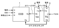
- FIG. 2 is a wiring diagram of the solid-state imaging device shown in FIG.
- the CCD image sensor chip 1 originally has a horizontal CCD drive signal ( ⁇ H1, ⁇ H2, ⁇ HL, ⁇ R) input terminal 10a, a vertical CCD drive signal ( ⁇ V1 to ⁇ V20) input terminal 12a, a power supply terminal 13, GND.
- a total of 27 signal terminals including a terminal 14 and a video output terminal 18 are provided.
- a clock input, a synchronization signal input, or the like may be added as necessary.
- the horizontal CCD drive signal input terminal 10 a is electrically connected to the output terminal 10 b of the timing generator chip 3 via the micro bumps 6.
- the vertical CCD drive signal input terminal 12 a is electrically connected to the output terminal 12 b of the CCD driver chip 4 through the micro bump 6.
- the power terminal 13 is configured as a power pad 5a
- the GND terminal 14 is configured as a GND pad 5b
- the video output terminal 18 is configured as a video output pad 5c.
- the power supply terminal 15 of the CCD driver chip 4 and the power supply terminal 16 of the timing generator chip 3 are connected to the power supply pad 5 a through the micro bumps 6.
- the control signal (TGCN) input terminal 17 of the timing generator chip 3 is connected to the control pad 5 d through the micro bump 6.
- the CCD image sensor chip 1 originally has a total of 27 signal terminals, but the timing generator chip 3 and the CCD driver chip 4 are flip-chip mounted on the CCD image sensor chip 1 via the micro bumps 6.
- a total of seven pads 5 are required for the solid-state imaging device. That is, only three power supply pads 5a, one GND pad 5b, one video output pad 5c, and three control pads 5d are required.
- the package cost and the cost of the mounting substrate can be significantly reduced.
- the flip chip mounting by the micro bumps 6 has a low resistance due to a short connection distance between the chips, and a parasitic inductance and a parasitic capacitance are reduced, so that high-speed pulse transmission is possible. Further, the mounting volume can be significantly reduced as compared with the conventional wire bonding connection.
- the CCD image sensor chip 1, the timing generator chip 3 and the CCD driver chip 4 are each formed with pads for connecting to the micro bumps 6. Under this pad, it is preferable to form a wiring layer other than the wiring layer forming the pad, and an element such as a transistor, a resistor, or a capacitor. This makes it possible to design the size of each chip smaller.
- the timing generator chip 3 and the CCD driver chip 4 are mounted as peripheral circuit elements. This is because it is generally difficult to make these semiconductor elements into one chip by the same process. These may be mounted on a single chip, which is preferable for miniaturization.
- FIG. 3 is a cross-sectional view showing a modification of the configuration of the solid-state imaging device according to the present embodiment.
- a protrusion 31 is provided around the imaging region 1 a, and the glass 2 as a transparent material is fixed to the protrusion 31 with, for example, an adhesive. That is, the glass 2 covers the imaging region 1 a so as to be supported by the protrusions 31, and a hollow portion 32 is formed between the imaging region 1 a and the glass 2.
- the hollow portion 32 is filled with, for example, air or nitrogen. Even in the configuration of FIG. 3, the imaging region 1a can be protected from dust and stress by the glass 2 in the manufacturing process or when used as a product.
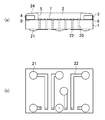
- FIG. 4A and 4B are diagrams showing a configuration of a solid-state imaging device according to Embodiment 2, in which FIG. 4A is a side view and FIG. 4B is a bottom view.
- FIG. 4A is a side view
- FIG. 4B is a bottom view.
- the top view since it is substantially the same as the above-mentioned Embodiment 1 except the peripheral part of the glass 2 being filled with the sealing resin 24, it is abbreviate
- 20 is a through electrode for electrically connecting the main surface and the back surface of the CCD image sensor chip 1
- 21 is a bump as a connection terminal formed on the back surface of the CCD image sensor chip 1
- 22 is a through electrode.
- 20 is a wiring for connecting 20 and the bump 21.
- the pad 5 formed on the main surface is electrically connected to the bump 21 formed on the back surface through the through electrode 20 and the wiring 22.
- the bump 21 may be formed below the through electrode 20 or may be formed at a position avoiding the bottom of the through electrode 20.
- the through electrode 20 and the wiring 22 are electrically insulated from the CCD image sensor chip 1 via an insulating film.
- the solid-state imaging device can be mounted on a printed board or a flexible board without wire bonding. For this reason, it becomes possible to reduce the volume after mounting remarkably compared with the mounting by the conventional wire bond.
- a sealing resin 24 is formed on the periphery of the glass 2 so as to cover the timing generator chip 3 and the CCD driver chip 4 which are flip-chip mounted. As a result, it is possible to prevent light from entering the timing generator chip 3 and the CCD driver chip 4 outside the imaging region, so that problems such as flare and ghost can be prevented.
- FIG. 5 shows a method for manufacturing a solid-state imaging device according to the third embodiment.
- the solid-state imaging device shown in FIG. 1 is manufactured.
- a wafer on which a solid-state image sensor (CCD image sensor chip 1) is formed is prepared. Before mounting, probe inspection of the solid-state imaging device on the wafer is performed (a).
- a dam 9 is formed in the solid-state image sensor on the wafer (b).
- the dam 9 may be formed by, for example, patterning by exposure and development using a photosensitive resin.
- the dam material may be applied to the entire surface of the wafer, and necessary portions may be formed by lithography and etching in the same manner as a general semiconductor process.
- the adhesive 7 is dropped on the inside of the dam 9, that is, on the imaging region (c). At this time, an appropriate amount of the adhesive 7 must be dropped so as not to overflow the dam 9 and leak outside.
- the adhesive 7 may be either an ultraviolet curable type or a heat curable type, but an ultraviolet curable type is desirable for curing while aligning in a subsequent bonding step.
- the glass 2 as a transparent material is bonded so as to cover the imaging region (d).
- the sealant 8 is dropped on the flip chip mounting area outside the imaging area (e).
- the sealant 8 used at this time is desirably transparent so that alignment is possible when flip-chip mounting is performed.
- the timing generator chip 3 on which the micro bumps are formed and the CCD driver chip 4 are flip-chip mounted (f).
- the tip of the microbump is sharpened at an acute angle, and when mounted, the microbump penetrates the sealant 8 and reaches the flip chip mounting pad of the CCD image sensor chip 1. At this time, it is desirable to form a high-quality ohmic contact by applying pressure while applying ultrasonic waves.
- the peripheral circuit element is attached and mounted, thereby eliminating the problem of dust getting on the imaging region.
- the influence of dust on the imaging region can be avoided.
- the imaging region can be protected from stress applied when mounting.
- the through electrode process is applied after the probe inspection in FIG. 5A and before the dam formation in FIG. 5B. Then, the through electrode, the wiring, and the bump on the back surface may be formed. Further, the through electrode process may be performed after glass bonding or flip chip mounting.
- each of the inspection pad and the micro bump bonding pad has a minimum area.
- test pads for the solid-state imaging device it is not necessary to arrange the number of test pads for the solid-state imaging device so that all the functions are inspected, and it is preferable that the number is sufficient to inspect some important functions. Thereby, it can avoid that the area of a solid-state image sensor increases with a pad.
- the solid-state imaging device is a CCD image sensor chip.
- a CMOS sensor chip or an NMOS sensor chip may be used.
- the peripheral circuit elements to be flip-chip mounted are not limited to the timing generator chip and the CCD driver chip shown here, but other elements that control the imaging operation of the solid-state image sensor, and the video output of the solid-state image sensor For example, an AD converter, an analog front end, or a digital signal processor may be used.
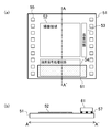
- FIG. 6 is a configuration diagram of a solid-state imaging device according to the fourth embodiment.
- (a) is a plan view and (b) is a sectional view taken along line AA ′ in (a).
- 51 is an image sensor chip as a solid-state image sensor.
- the image sensor chip 51 includes an imaging region 52 in which unit pixels including photoelectric conversion elements are formed in a matrix, a scanning circuit 53 that controls reading of the imaging region 52, and pixel signals read from the imaging region 52.
- a pixel signal processing circuit 54 for performing noise removal, AD conversion, and the like, and an input / output terminal 55 for performing input / output with the outside of the solid-state imaging device.
- the input / output terminal 55 is also provided with an internal circuit including a protection circuit composed of a high breakdown voltage transistor or the like.
- the image sensor chip 51 is a MOS image sensor such as a CMOS sensor chip or an NMOS sensor chip, a CCD image sensor chip, or the like.
- Reference numeral 61 denotes a signal processing chip as a signal processing element.
- the image sensor chip 51 and the main surface face each other in an area other than the imaging area 52 on the main surface of the image sensor chip 51. It is mounted and pasted together. That is, the signal processing chip 61 is flip-chip mounted on the image sensor chip 51 via a plurality of micro bumps 57, and an electrical path is formed between the signal processing chip 61 and the image sensor chip 51 at the mounting position. . Input / output between the signal processing chip 61 and the outside of the solid-state imaging device is performed via an electrical path formed by the micro bumps 57, an internal circuit of the image sensor chip 51, and an input / output terminal 55. The signal processing chip 61 is not provided with input / output terminals that directly input / output from / to the outside of the solid-state imaging device.
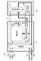
- FIG. 7 is a wiring diagram of the solid-state imaging device shown in FIG.
- the image sensor chip 51 includes, as input / output terminals 55, power input terminals 55a and 55b for a plurality of power supplies (here, power supplies A and B) having different voltages, a control signal input terminal 55c, and an image.
- An output terminal 55d is provided.
- a protection circuit 56 as an internal circuit is provided.
- the protection circuit 56 may include a level shifter circuit for voltage conversion.
- the signal processing chip 61 includes only a logic circuit, and includes a timing generation circuit 62 that controls driving of the image sensor chip 51 and the like, and a signal processing circuit 63 that processes signals from the image sensor chip 51. ing.
- the signal processing chip 61 receives the power supply, control signal, and video output supplied from the image sensor chip 51 via the micro bumps 57. Further, the signal processing chip 61 outputs the video output processed by the signal processing circuit 63 to the image sensor chip 51 through the micro bumps 57. That is, the image output of the image sensor chip 51 is transmitted to the signal processing chip 61 via the micro bumps 57, processed in the signal processing chip 61, and then again passed through the micro bumps 57 to the image sensor chip 51. Is transmitted to. Then, the image is output from the video output terminal 55d to the outside of the solid-state imaging device via the protection circuit 56 of the image sensor chip 51.
- the solid-state imaging device for electrical connection between the image sensor chip 51 and the signal processing chip 61, a complicated configuration such as a back-illuminated solid-state imaging device, a through wiring structure, a multilayer substrate, or the like. Is no longer necessary. For this reason, the solid-state imaging device can be reduced in size and cost.
- the video output after the signal processing by the signal processing chip 61 is output from the output circuit of the image sensor chip 51, a high breakdown voltage transistor for the output circuit is formed in the signal processing chip 61. There is no need to do. For this reason, the chip size can be further reduced.
- the signal processing chip 61 composed of only the logic circuit to be supplied with a power supply having a low voltage necessary for the operation of the logic circuit. Therefore, in the present embodiment, the lowest voltage power source (here, power source A) among the power sources supplied to the image sensor chip 51 is supplied to the signal processing chip 61 via the micro bumps 57.
- the transistor of the signal processing chip 61 can be configured with a transistor of a thin gate oxide film corresponding to a low voltage power source. This makes it possible to produce a low-cost signal processing chip 61 with a simple manufacturing process, in addition to the need for the high breakdown voltage transistor for the protection circuit as described above.
- the wiring layout rules and the number of wiring layers of the image sensor chip 51 and the signal processing chip 61 can be optimized. Specifically, in the signal processing chip 61 configured only with logic circuits and driven at a low voltage, wiring and transistors are laid out using fine wiring rules, and the number of wiring layers is increased in accordance with the circuit scale. It is sufficient to improve the coverage ratio. Thereby, the signal processing chip 61 can be significantly reduced in size. In this case, the number of wiring layers of the signal processing chip 61 is larger than the number of wiring layers of the image sensor chip 51.
- FIG. 8 is a wiring diagram of the solid-state imaging device according to the fifth embodiment.
- the configuration diagram of the solid-state imaging device according to the present embodiment is the same as FIG. In FIG. 8, the same components as those in FIG. 7 are denoted by the same reference numerals as those in FIG. 7, and detailed description thereof is omitted here.
- the signal processing chip 61 is flip-chip mounted via a plurality of micro bumps 57 in a region other than the imaging region 52 on the main surface of the image sensor chip 51, as shown in FIG.
- An electrical path is formed between the mounting portion and the image sensor chip 51.
- Input / output between the signal processing chip 61 and the outside of the solid-state imaging device is performed via an electrical path formed by the micro bumps 57, an internal circuit of the image sensor chip 51, and an input / output terminal 55.
- the difference from the fourth embodiment is that the image sensor chip 51 is configured to be able to output a plurality of rows of image signals in the imaging region 52 in parallel.
- the signal processing chip 61 includes only a logic circuit, and includes a timing generation circuit 63 that controls driving of the image sensor chip 51 and the like, and a column that processes a plurality of columns of image signals output from the image sensor chip 51.
- a signal processing circuit 64 and a signal processing circuit 65 that processes the signal processed by the column signal processing circuit 64 again are provided.
- FIG. 9 is a detailed wiring diagram showing signal connections between the pixel signal processing circuit 54 of the image sensor chip 51 and the column signal processing circuit 64 and the signal processing circuit 65 of the signal processing chip 61.
- the pixel signal processing circuit 54 compares the pixel signal output from the imaging region 52 with the ramp waveform and performs AD conversion, and the AD converted output voltage as a signal processing chip 61.
- a level shifter 92 for converting to a low voltage that can be processed.
- the comparator 91 and the level shifter 92 are provided in each column of the imaging area 52.
- micro bumps 57 for transmitting the output of the level shifter 92, that is, the image signals of each column to the signal processing chip 61 are provided.
- the column signal processing circuit 64 includes a digital memory 93 provided corresponding to the microbump 57 and a horizontal scanning circuit 94 for selecting the digital memory 93 for reading.
- the digital memory 93 stores the image signal received via the micro bump 57 as a digital signal of 8 to 14 bits.
- the digital signals stored in the digital memory 93 are sequentially selected by the horizontal scanning circuit 94 and transmitted to the signal processing circuit 65 as a digital output.
- the signal processing circuit 65 performs signal processing such as black correction and scratch correction.
- the image signal after the signal processing is transmitted again to the image sensor chip 51 via the micro bumps 57 and then output as a video output via the input / output terminal of the image sensor chip 51.
- the micro bumps 57 can be arranged at a narrow pitch, by providing the micro bumps 57 for respectively transmitting a plurality of rows of image signals, A plurality of columns of image signals can be transferred in parallel with the signal processing chip 61.
- the microbump 57 has a low resistance because of a short connection distance between chips, and has a small parasitic inductance and parasitic capacitance. Therefore, high-speed and low power consumption signal transmission is possible.
- the pixel signal processing circuit 54 configured by an analog circuit such as the comparator 91 that requires a high voltage to obtain a wide dynamic range and a high S / N ratio is disposed on the image sensor chip 51 side.
- the column signal processing circuit 64 including the digital memory 93 operable at a low voltage is arranged on the signal processing chip 61 side constituted only by the digital circuit.
- the signal processing chip 61 can be composed of only a transistor having a thin gate oxide film corresponding to a low power supply, and the type of transistor used in each chip can be optimized. Therefore, it is possible to create a low-cost solid-state imaging device with a simple manufacturing process.
- the signal processing chip 61 improves the coverage ratio by laying out wiring / transistors using an optimal fine wiring rule and further increasing the number of wiring layers according to the circuit scale.
- the area of the column signal processing circuit 64 on which many logic circuits such as the digital memory 93 composed of a large number of latch circuits and the like for storing multi-bit digital signals is mounted on the image sensor chip 51. Compared to the case, the size can be significantly reduced.
- the image signals in each column of the imaging region 52 are transmitted to the signal processing chip 61 via the corresponding micro bumps 57, but the present invention is not limited to this.
- a selector is provided between the level shifter 92 and the microbump 57, and a plurality of rows are associated with one microbump 57 and an image signal is selectively output to the signal processing chip 61 via the microbump 57. You may do it. This is effective when the pitch of each column of the imaging region 52 does not match the pitch at which the micro bumps 57 can be arranged.
- the fourth and fifth embodiments an example is shown in which one signal processing element is mounted on the solid-state imaging device. However, if the imaging region is outside the imaging region, a plurality of signal processing elements are mounted on the solid-state imaging device. It doesn't matter. For example, by mounting a digital signal processor, it is possible to realize a solid-state imaging camera as a chip set.
- the solid-state imaging device can be reduced in size and cost, for example, a high-speed, low power consumption, compact and low-cost digital camera, movie camera, etc. can be realized, which is useful.
Landscapes
- Engineering & Computer Science (AREA)
- Multimedia (AREA)
- Signal Processing (AREA)
- Solid State Image Pick-Up Elements (AREA)
- Transforming Light Signals Into Electric Signals (AREA)
Abstract
固体撮像素子(1)は、光電変換素子を含む単位画素が行列状に形成された撮像領域(1a)を主面上に有している。周辺回路素子(3,4)は固体撮像素子(1)の撮像動作の制御、または、固体撮像素子(1)の映像出力の信号処理を行う。撮像領域(1a)は、透明材料(2)によって覆われている。周辺回路素子(3,4)は、固体撮像素子(1)の主面上における撮像領域(1a)以外の領域に、その主面が固体撮像素子(1)の主面と対向するように実装されている。
Description
本発明は、小型・低コストの固体撮像デバイスおよびその製造方法に関する。
近年、固体撮像デバイスとして、小型化、低消費電力化、信号処理の高速化を実現するために、例えば特許文献1では、図10に示すように、センサブロック151と信号処理ブロック152を同一半導体基板内に構成した固体撮像装置が報告されている。またこの構成をベースとして、さらに小型化・高速化を実現するために、SIP(System in Package)という、固体撮像素子とその周辺回路である複数のチップとを半導体モジュールとして一体に実装した形態が報告されている。
例えば特許文献2では、図11に示すような、固体撮像素子112と周辺回路素子111とを積層実装し、固体撮像素子112と周辺回路素子111の電気的接続を積層基板110を介して行う、という構成が開示されている。
また、例えば特許文献3では、図12に示すように、信号処理チップ153上に、裏面照射型CMOSイメージセンサチップ154をマイクロバンプ155によって積層実装し、信号処理チップ153から信号の入出力を行うという構成が開示されている。
また、固体撮像デバイスではないが一般の半導体デバイスとして、特許文献4では、異なる半導体素子の主面同士を対向させて接続するCOC(Chip on Chip)技術により、小型化を実現した構成が開示されている。
図11の構成では、積層基板110に周辺回路素子111をフリップチップ実装し、この周辺回路素子111の裏面に固体撮像素子112を実装し、固体撮像素子112と積層基板110をワイヤーボンドで接続している。しかしながら近年、固体撮像素子の入出力端子数が増加してきたため、図11のような構成では、積層基板の配線密度が高くなるため高コストになる、あるいは、多数の入出力端子のワイヤボンドの領域が必要となるためそれほど小型化ができない、といった問題が生じる。
また、特許文献4に開示されたCOC技術を固体撮像デバイスに採用した場合には、固体撮像素子に周辺回路素子を実装する際に、撮像領域にダストが乗ってしまう、あるいは、撮像領域に応力がかかってしまう、といった問題が生じる。このため、性能や歩留まりの低下を招く可能性があり、実現が困難であった。
また、図10の構成では、同一半導体基板の中で複数種類のゲート絶縁膜のトランジスタが必要となるため、プロセスが複雑となる。また複雑な機能をもつ信号処理ブロックを同一半導体基板に搭載すると、回路間を接続する配線の数が増加するため、配線層数を増やすか、または配線が占める面積を大きくする必要がある。
しかし、配線層数を増やした場合には、光を受光するフォトダイオードから配線層最上層で決まる開口部までの距離が高くなり、斜め光がさえぎられ感度が低下するという問題が発生する。特に、画素のセルサイズ(ピッチ)が小さくなると、配線層数を増やすことのデメリットがますます大きくなる。
一方、配線が占める面積を大きくすることは、固体撮像装置のサイズ増大に直結する。例えば信号処理回路について、一般のシステムLSIで使用されている5~6層の配線層を採用した場合、トランジスタレイアウトと配線で決まるトランジスタの敷き占め率は80%程度である。これに対して、上述の感度低下の問題を考慮して、イメージセンサで一般に使用されている3層の配線層を採用した場合には、トランジスタの敷き占め率が30~40%程度に低下し、このため、信号処理回路の面積が2倍強に増大してしまう。
また、図12の構成では、信号処理チップ153上にイメージセンサチップ154を積層実装することによって、上述したチップサイズ増大の問題に対処している。ところがこの場合、信号処理チップ153の回路面とイメージセンサチップ154の回路面とを向かい合わせて張り合わせる必要があるので、イメージセンサチップ154として、受光面と回路面が異なる裏面照射型イメージセンサを用いる、という複雑な構成となっている。
また、信号処理チップ153を基板としてイメージセンサチップ154を搭載しているために、一般に使用電圧の高いイメージセンサチップ154で使用する電圧を、信号処理チップ153でも受け取る必要がある。
さらには、その他のSIP構造の構成として、固体撮像素子を信号処理素子に重ねて貼り付け、固体撮像素子の基板に貫通配線を通し、マイクロバンプを用いて下側の信号処理素子に電気的に接続する例がある。ところがこの場合にも、図12の構成と同様に、複雑な構成の固体撮像素子が必要となる。
またその他の構成では、固体撮像素子を信号処理素子に重ねて貼り付け、この両素子を回路基板上に配置し、各素子と回路基板間をワイヤボンディングし、このワイヤボンディングにより両素子間を電気的に接続する例がある。ところがこの構成では、入出力端子が微細化できず小型化に向いていない、またワイヤボンドのインピーダンスにより高速化に向いていない、という問題がある。
さらに近年では、システムLSIの微細プロセス化が進み、光学サイズにより撮像領域が一義的に決定されるような固体撮像素子に対して、信号処理回路の面積は大幅に縮小している。このため、実際のデバイスでは、信号処理素子の入出力端子数によってチップサイズが決定されている、という実態がある。
前記の問題に鑑み、本発明は、撮像領域にダストや応力の影響を与えることなく、固体撮像デバイスの小型化を実現することを目的とする。
また、本発明は、前記従来の問題を解決し、固体撮像素子と信号処理素子を備えた固体撮像デバイスにおいて、より一層の小型化・低コスト化を実現することを目的とする。
本発明の一態様では、固体撮像デバイスとして、光電変換素子を含む単位画素が行列状に形成された撮像領域を主面上に有する固体撮像素子と、前記固体撮像素子の撮像動作の制御または前記固体撮像素子の映像出力の信号処理を行う周辺回路素子とを備え、前記周辺回路素子は、前記固体撮像素子の主面上における前記撮像領域以外の領域に、その主面が前記固体撮像素子の主面と対向するように貼り合わされて実装されており、前記撮像領域は透明材料によって覆われている。
この態様によると、周辺回路素子が、固体撮像素子の撮像領域以外の領域に、主面同士が対向するように貼り合わされて実装されているので、固体撮像素子と周辺回路素子との電気的接続のために積層基板やワイヤボンドが不要となるため、固体撮像デバイスの小型化および低コスト化が可能になる。また、固体撮像素子と周辺回路素子との間で、近年のバンプ形成技術の進展により、多数の入出力端子の接続が可能となるので、データ転送を並列に行うことができ、高速・低消費電力化が実現できる。さらに、固体撮像素子の撮像領域が透明材料によって覆われているため、実装する際における、撮像領域へのダストの影響を回避することができるとともに、撮像領域にかかる応力もこの透明材料によって緩和することが可能になる。
また、前記態様に係る固体撮像デバイスにおいて、前記透明材料は、前記撮像領域の表面に接着剤によって接着されているのが好ましい。これにより、実装する際における、撮像領域にかかる応力を、より効果的に緩和することが可能になる。
また、前記態様に係る固体撮像デバイスにおいて、前記固体撮像素子は、主面と裏面とを電気的に接続する貫通電極と、裏面上に形成されており、前記貫通電極と電気的に接続された接続端子とを備えているのが好ましい。これにより、固体撮像素子の裏面を基板に貼り付けるだけで、電気的接続が実現されるので、この固体撮像デバイスを例えばカメラ等に実装する場合に、その実装コストや実装体積を低減することが可能となる。
また、本発明の一態様では、固体撮像デバイスの製造方法として、光電変換素子を含む単位画素が行列状に2次元配列されてなる撮像領域を主面上に有する固体撮像素子が形成された、ウエハを準備する工程と、前記固体撮像素子の撮像領域を覆うように透明材料を設ける工程と、前記透明材料を設けた後に、前記固体撮像素子の撮像動作の制御、または、前記固体撮像素子の映像出力の信号処理を行う周辺回路素子を、前記固体撮像素子の主面上における前記撮像領域以外の領域に、その主面が前記固体撮像素子の主面と対向するように、貼り合わせて実装する工程とを備えている。
この態様によると、固体撮像素子の撮像領域を覆うように透明材料を設けた後に、周辺回路素子が、固体撮像素子の撮像領域以外の領域に、主面同士が対向するように貼り合わされて実装される。このため、実装する際における、撮像領域へのダストの影響を回避できるとともに、撮像領域にかかる応力もこの透明材料によって緩和することが可能になる。
また、本発明の一態様では、固体撮像デバイスとして、光電変換素子を含む単位画素が行列状に形成された撮像領域を主面上に有する固体撮像素子と、前記固体撮像素子の映像出力の信号処理を行う回路を主面上に有した信号処理素子とを備え、前記信号処理素子は、前記固体撮像素子の主面上における前記撮像領域以外の領域に、主面同士が対向するように貼り合わせて実装され、実装箇所において前記固体撮像素子との間に電気的経路が形成されており、前記信号処理素子と当該固体撮像デバイス外部との間の入出力は、前記電気的経路と、前記固体撮像素子の内部回路および入出力端子とを介して行われるように、構成されている。
この態様によると、信号処理素子が、固体撮像素子の撮像領域以外の領域に実装されており、かつ、実装箇所において電気的経路が形成されているので、固体撮像素子と信号処理素子との電気的接続のために、裏面照射型固体撮像素子や貫通配線構造、積層基板等の複雑な構成が不要となる。このため、固体撮像デバイスの小型化および低コスト化が可能になる。さらに、信号処理素子は、固体撮像デバイス外部との入出力は、固体撮像素子の内部回路および入出力端子を介して行われる。このため、信号処理素子において、入出力の保護回路の省略、簡素化が可能となり、また、高耐圧のトランジスタを形成する必要がなくなるので、大幅な小型化・低コスト化が実現できる。
本発明によると、周辺回路素子の実装において、撮像領域へのダストの影響を回避できるとともに撮像領域にかかる応力も緩和できるので、性能や歩留まりの低下を招くことなく、固体撮像デバイスの小型化を実現することができる。
また、本発明によると、固体撮像素子と信号処理素子を有する固体撮像デバイスのより一層の小型化・低コスト化を実現することができる。
以下、本発明の実施の形態について、図面を用いて詳細に説明する。
(実施の形態1)
図1は実施の形態1に係る固体撮像デバイスの構成を示す図である。同図中、(a)は平面図、(b)は(a)の線A-A’における断面図である。図1において、1は固体撮像素子としてのCCD(Charge Coupled Device)イメージセンサチップである。CCDイメージセンサチップ1は、光電変換素子と垂直CCDとで構成された単位画素が行列状に形成された撮像領域1aを、その主面上に有している。垂直CCDは信号電荷を垂直方向に転送する。また、図示していないが、CCDイメージセンサチップ1はさらに、水平方向の電荷転送を行う水平CCDと、信号電荷を信号電圧に変換して外部に出力する検出部とを備えている。
図1は実施の形態1に係る固体撮像デバイスの構成を示す図である。同図中、(a)は平面図、(b)は(a)の線A-A’における断面図である。図1において、1は固体撮像素子としてのCCD(Charge Coupled Device)イメージセンサチップである。CCDイメージセンサチップ1は、光電変換素子と垂直CCDとで構成された単位画素が行列状に形成された撮像領域1aを、その主面上に有している。垂直CCDは信号電荷を垂直方向に転送する。また、図示していないが、CCDイメージセンサチップ1はさらに、水平方向の電荷転送を行う水平CCDと、信号電荷を信号電圧に変換して外部に出力する検出部とを備えている。
CCDイメージセンサチップ1の撮像領域1aは、透明材料としてのガラス2によって覆われている。ガラス2は、撮像領域1aの表面に、接着剤7によって接着されている。また、ガラス2を接着する際に接着剤7が撮像領域1a以外の領域に流れ出すのを防ぐために、撮像領域1aの周囲にダム9が形成されている。
3は周辺回路素子としての、CCDイメージセンサチップ1の水平CCDおよび垂直CCDを駆動するタイミングを制御するためのタイミングジェネレータチップである。4は周辺回路素子としての、垂直CCDを駆動するためのCCDドライバチップである。タイミングジェネレータチップ3およびCCDドライバチップ4は、CCDイメージセンサチップ1の主面上における撮像領域1a以外の領域に、その主面がCCDイメージセンサチップ1の主面と対向するように、貼り合わされて実装されている。具体的には、CCDイメージセンサチップ1とタイミングジェネレータチップ3およびCCDドライバチップ34とは、マイクロバンプ6によって電気的に接続されている。また、フリップチップ実装されたチップ1,3,4の信頼性を確保するために、封止剤8が挿入されている。なお図1では、チップ3,4は撮像領域1aの両サイドに実装されているが、実装される位置はこれに限られるものではない。
5はCCDイメージセンサチップ1に形成された入出力パッドである。5aはチップ1,3,4に電源を供給するための電源パッドであり、ここでは例えば、電源電圧-7V、3.3V、12Vにそれぞれ対応した3つの電源パッド5aが設けられている。5bはGNDパッドであり、電源パッド5aと同様に、チップ1,3,4に接続されている。5cは映像出力パッドであり、撮像された映像信号を出力する。5dはタイミングジェネレータチップ3の制御パッドである。制御パッド5dには、例えばCCDイメージセンサチップ1の駆動モードを選択するための制御信号が入力される。タイミングジェネレータチップ3は、この制御信号によって選択されたモードに応じて、駆動するタイミングを制御する。
図1の構成では、撮像領域1aの表面が、透明材料としてのガラス2で覆われている。これにより、この固体撮像デバイスの製造工程において、フリップチップ実装を行う際に生じるダストが撮像領域1aに乗る、という問題が生じず、ダストの影響を回避することができる。また、ガラス2は、撮像領域1aの表面に接着剤7によって接着されているので、撮像領域1aにかかる応力を緩和する役割も果たす。すなわち、ガラス2を設けることによって、フリップチップ実装を行う際にかかる応力から撮像領域1aを保護することが可能になる。またもちろん、この固体撮像デバイスが製品として使用されている際にも、このガラス2によって、撮像領域1aをダストや応力から保護することができる。なお、ここでは、透明材料の一例としてガラスを示したが、透明材料はガラスに限られるものではなく、例えばアクリルであってもよい。
図2は図1に示す固体撮像デバイスの配線図である。図2に示すように、CCDイメージセンサチップ1は元々、水平CCD駆動信号(φH1、φH2、φHL、φR)入力端子10a、垂直CCD駆動信号(φV1~φV20)入力端子12a、電源端子13,GND端子14、および映像出力端子18の計27個の信号端子を有している。なお、ここでは、固体撮像素子の信号端子として最小限のものを示したが、必要に応じてクロック入力や同期信号入力などを付加してもよい。
これらのうち、水平CCD駆動信号入力端子10aは、タイミングジェネレータチップ3の出力端子10bとマイクロバンプ6を介して電気的に接続されている。垂直CCD駆動信号入力端子12aは、CCDドライバチップ4の出力端子12bとマイクロバンプ6を介して電気的に接続されている。また、電源端子13は電源パッド5aとして、GND端子14はGNDパッド5bとして、映像出力端子18は映像出力パッド5cとして、構成されている。CCDドライバチップ4の電源端子15およびタイミングジェネレータチップ3の電源端子16は、マイクロバンプ6を介して電源パッド5aと接続されている。さらに、タイミングジェネレータチップ3の制御信号(TGCN)入力端子17は、マイクロバンプ6を介して制御パッド5dと接続されている。
このように、CCDイメージセンサチップ1は元々計27個の信号端子を有しているが、CCDイメージセンサチップ1にタイミングジェネレータチップ3およびCCDドライバチップ4をマイクロバンプ6を介してフリップチップ実装することによって、本固体撮像デバイスに必要なパッド5は計7個になる。すなわち、3個の電源パッド5aと、1個のGNDパッド5bと、1個の映像出力パッド5cと、3個の制御パッド5dとだけで済む。これにより、この固体撮像デバイスを例えばカメラ等に実装する工程において、パッケージコストや実装基板のコストを大幅に低減することができる。
また、マイクロバンプ6によるフリップチップ実装は、チップ間の接続距離が短いため低抵抗でありかつ寄生インダクタンスや寄生容量も少なくなるため、高速のパルス伝達が可能となる。また従来のワイヤボンドによる接続に比べて、実装体積も大幅に低減することができる。
なお、CCDイメージセンサチップ1とタイミングジェネレータチップ3およびCCDドライバチップ4とには、それぞれ、マイクロバンプ6と接続するためのパッドが形成されている。このパッドの下には、パッドを形成する配線層以外の配線層や、トランジスタ、抵抗、キャパシタ等の素子を形成することが好ましい。これにより、それぞれのチップのサイズをより小さく設計することが可能になる。
なお、本実施形態では、周辺回路素子としてタイミングジェネレータチップ3とCCDドライバチップ4とを実装したが、これは一般的にこれらの半導体素子の同一プロセスによる1チップ化が困難であるためであり、これらが1チップ化されたものを実装してよく、小型化にはその方が好ましい。
図3は本実施形態に係る固体撮像デバイスの構成の変形例を示す断面図である。図3の構成では、撮像領域1aの周囲に突部31が設けられており、この突部31に例えば接着剤によって透明材料としてのガラス2が固定されている。すなわち、ガラス2は突部31に支えられるようにして撮像領域1aを覆っており、撮像領域1aとガラス2との間に中空部32が形成されている。中空部32は例えば空気や窒素によって満たされている。図3の構成でも、製造工程において、あるいは、製品として使用されている場合において、ガラス2によって、撮像領域1aをダストや応力から保護することができる。
(実施の形態2)
図4は実施の形態2に係る固体撮像デバイスの構成を示す図であり、同図中、(a)は側面図、(b)は底面図である。なお、平面図については、上述の実施の形態1とは、ガラス2の周辺部が封止樹脂24で充填されている以外はほぼ同一であるので、ここでは省略している。
図4は実施の形態2に係る固体撮像デバイスの構成を示す図であり、同図中、(a)は側面図、(b)は底面図である。なお、平面図については、上述の実施の形態1とは、ガラス2の周辺部が封止樹脂24で充填されている以外はほぼ同一であるので、ここでは省略している。
図4において、20はCCDイメージセンサチップ1の主面と裏面とを電気的に接続する貫通電極、21はCCDイメージセンサチップ1の裏面上に形成された接続端子としてのバンプ、22は貫通電極20とバンプ21とを接続するための配線である。主面上に形成されたパッド5は、貫通電極20および配線22を介して、裏面上に形成されたバンプ21と電気的に接続されている。なお、バンプ21は、貫通電極20下に形成してもよいし、貫通電極20下を避けた位置に形成してもよい。なお、図示は省略したが、貫通電極20および配線22は、CCDイメージセンサチップ1とは絶縁膜を介して電気的に絶縁されている。
このような構成により、固体撮像デバイスを、ワイヤボンドなしで、プリント基板やフレキシブル基板に実装することができる。このため、従来のワイヤボンドによる実装に比べて格段に、実装後の体積を低減することが可能となる。
また、封止樹脂24が、ガラス2の周辺部に、フリップチップ実装したタイミングジェネレータチップ3やCCDドライバチップ4を覆うように形成されている。これにより、撮像領域外のタイミングジェネレータチップ3やCCDドライバチップ4に光が入射することを防止できるので、フレアやゴーストといった不具合を防止することができる。
(実施の形態3)
図5は実施の形態3に係る固体撮像デバイスの製造方法を示す図である。図5では、図1に示す固体撮像デバイスを製造するものとしている。
図5は実施の形態3に係る固体撮像デバイスの製造方法を示す図である。図5では、図1に示す固体撮像デバイスを製造するものとしている。
まず、固体撮像素子(CCDイメージセンサチップ1)が形成されたウエハを準備する。そして実装の前に、ウエハ上の固体撮像素子のプローブ検査を行う(a)。
次に、ウエハ上の固体撮像素子にダム9を形成する(b)。ダム9の形成は例えば、感光性の樹脂を用いて、露光現像によるパターニングによって行えばよい。あるいは、ダム材料をウエハ全面に塗布し、必要な部分を一般の半導体プロセスと同様に、リソグラフィとエッチングによって形成してもよい。
次に、ダム9の内部すなわち撮像領域上に接着剤7を滴下する(c)。このとき、接着剤7は、ダム9を溢れて外部に漏れないように適量を滴下しなければならない。また、接着剤7は、紫外線硬化型または熱硬化型のどちらでもよいが、後の接着工程において位置合わせをしながら硬化させるには、紫外線硬化型が望ましい。
次に、透明材料としてのガラス2を、撮像領域を覆うように接着する(d)。このとき、ガラス2の貼り合わせ位置を制御できるように、ガラス2の位置を合わせた後に、紫外線を照射して接着剤7を硬化させるのが好ましい。
次に、封止剤8を、撮像領域外のフリップチップ実装する領域に滴下する(e)。このとき使用する封止剤8は、フリップチップ実装するときに位置合わせが可能なように、透明であることが望ましい。
次に、マイクロバンプが形成されたタイミングジェネレータチップ3とCCDドライバチップ4をフリップチップ実装する(f)。マイクロバンプの先端が鋭角に尖っており、実装されたとき、封止剤8を貫通して、CCDイメージセンサチップ1のフリップチップ実装用のパッドに到達する。さらにこのとき、超音波を掛けながら加圧することによって、良質のオーミックコンタクトを形成することが望ましい。
最後に、ダイシング工程によって(g)、ウエハから個片の固体撮像素子を形成する。
このように、固体撮像素子の撮像領域を覆うように透明材料を設けて、透明材料を設けた後に、周辺回路素子を貼り合わせて実装することによって、ダストが撮像領域に乗るという問題が生じなくなり、撮像領域へのダストの影響を回避することができる。また、実装を行う際にかかる応力から、撮像領域を保護することが可能になる。
なお、もちろんのことであるが、ガラス接着工程やフリップチップ実装工程は、最初のプローブ検査で良品になった固体撮像素子にのみ行うのが、コスト上望ましい。
また、実施の形態2に対応した製造方法はここでは図示しなかったが、例えば、図5(a)のプローブ検査の後、図5(b)のダム形成の前に、貫通電極プロセスを適用して貫通電極および配線、裏面のバンプを形成すればよい。また、貫通電極プロセスをガラス接着やフリップチップ実装の後で行っても良い。
なお、プローブ検査用のパッドとマイクロバンプを介して接合するパッドとは別にして、マイクロバンプが検査針跡の影響を受けにくいようにすることが望ましい。このとき、検査用パッドとマイクロバンプ接合用のパッドはそれぞれ、最小の面積にするのが望ましい。
また固体撮像素子の検査用パッドは、その全機能を検査するだけの数を配置する必要はなく、一部の重要な機能を検査するに足る数に抑えておくのが好ましい。これにより、固体撮像素子の面積がパッドにより増大することを回避することができる。
なお、以上の第1~第3の実施形態では、固体撮像素子はCCDイメージセンサチップとしたが、この他例えば、CMOSセンサチップ、NMOSセンサチップでもかまわない。また、フリップチップ実装する周辺回路素子は、ここで示したタイミングジェネレータチップやCCDドライバチップに限られるものでなく、固体撮像素子の撮像動作の制御を行う他の素子や、固体撮像素子の映像出力の信号処理を行う素子、例えばADコンバータやアナログフロントエンド、デジタルシグナルプロセッサなどであっても良い。
(実施の形態4)
図6は実施の形態4に係る固体撮像デバイスの構成図である。同図中、(a)は平面図、(b)は(a)の線A-A’における断面図である。図6において、51は固体撮像素子としてのイメージセンサチップである。イメージセンサチップ51は、光電変換素子を含む単位画素が行列状に形成された撮像領域52と、撮像領域52の読み出しをコントロールする走査回路53と、撮像領域52から読み出された画素信号に対してノイズ除去やAD変換等を行う画素信号処理回路54と、固体撮像デバイス外部との入出力を行うための入出力端子55とを備えている。入出力端子55には、高耐圧のトランジスタ等で構成された保護回路を含む内部回路が併せて設けられている。イメージセンサチップ51は、CMOSセンサチップ、NMOSセンサチップ等のMOS型イメージセンサや、CCDイメージセンサチップ等である。
図6は実施の形態4に係る固体撮像デバイスの構成図である。同図中、(a)は平面図、(b)は(a)の線A-A’における断面図である。図6において、51は固体撮像素子としてのイメージセンサチップである。イメージセンサチップ51は、光電変換素子を含む単位画素が行列状に形成された撮像領域52と、撮像領域52の読み出しをコントロールする走査回路53と、撮像領域52から読み出された画素信号に対してノイズ除去やAD変換等を行う画素信号処理回路54と、固体撮像デバイス外部との入出力を行うための入出力端子55とを備えている。入出力端子55には、高耐圧のトランジスタ等で構成された保護回路を含む内部回路が併せて設けられている。イメージセンサチップ51は、CMOSセンサチップ、NMOSセンサチップ等のMOS型イメージセンサや、CCDイメージセンサチップ等である。
61は信号処理素子としての信号処理チップであり、図6(b)に示すように、イメージセンサチップ51の主面上における撮像領域52以外の領域に、イメージセンサチップ51と主面同士が対向するように貼り合わされて実装されている。すなわち、信号処理チップ61は、複数のマイクロバンプ57を介して、イメージセンサチップ51上にフリップチップ実装されており、その実装箇所においてイメージセンサチップ51との間に電気的経路が形成されている。そして、信号処理チップ61と固体撮像デバイス外部との間の入出力は、マイクロバンプ57によって形成された電気的経路と、イメージセンサチップ51の内部回路および入出力端子55とを介して行われる。信号処理チップ61には、固体撮像デバイス外部と直接的に入出力を行う入出力端子は設けられていない。
図7は図6に示す固体撮像デバイスの配線図である。図7に示すように、イメージセンサチップ51は、入出力端子55として、電圧が異なる複数の電源(ここでは電源A,B)向けの電源入力端子55a,55bと、制御信号入力端子55cおよび映像出力端子55dを備えている。また入出力端子55に併せて、内部回路としての保護回路56を備えている。この保護回路56は、電圧変換のためのレベルシフタ回路等を含んでいてもよい。また、信号処理チップ61は、ロジック回路のみで構成されており、イメージセンサチップ51等の駆動制御を行うタイミング発生回路62と、イメージセンサチップ51からの信号を処理する信号処理回路63とを備えている。
信号処理チップ61は、イメージセンサチップ51から供給された電源、制御信号および映像出力が、マイクロバンプ57を介して入力される。また、信号処理チップ61は、信号処理回路63によって処理された映像出力を、マイクロバンプ57を介してイメージセンサチップ51に出力する。すなわち、イメージセンサチップ51の映像出力は、マイクロバンプ57を経由して信号処理チップ61に伝達され、信号処理チップ61内で信号処理された後、再びマイクロバンプ57を経由してイメージセンサチップ51に伝達される。そして、イメージセンサチップ51の保護回路56を経由して、映像出力端子55dから固体撮像デバイス外部に出力される。
このように本実施形態によると、固体撮像デバイスにおいて、イメージセンサチップ51と信号処理チップ61との電気的接続のために、裏面照射型固体撮像素子や貫通配線構造、積層基板等の複雑な構成が不要となる。このため、固体撮像デバイスの小型化および低コスト化が可能になる。
また、信号処理チップ61と固体撮像デバイス外部との入出力は、イメージセンサチップ51の内部回路および入出力端子55を介して行われる。このため、信号処理チップ61に、高耐圧のトランジスタ等で構成される特別な保護回路を備える必要がない。したがって、信号処理チップ61のマイクロバンプ57を狭ピッチで配置できるため、信号処理チップ61のチップサイズが入出力端子数で決まってしまうという問題を回避することができる。
さらに、本実施形態によると、信号処理チップ61による信号処理後の映像出力は、イメージセンサチップ51の出力回路から出力されるので、信号処理チップ61に出力回路のための高耐圧のトランジスタを形成する必要がない。このため、チップサイズのより一層の小型化が実現できる。
さらに、ロジック回路のみで構成されている信号処理チップ61は、ロジック回路の動作に必要となる程度の低い電圧の電源が供給されていれば足りる。そこで本実施形態では、イメージセンサチップ51に供給される電源のうち最も低い電圧の電源(ここでは電源A)が、信号処理チップ61にマイクロバンプ57を介して供給されている。このような構成により、信号処理チップ61のトランジスタは、低電圧電源に対応した薄膜ゲート酸化膜のトランジスタで構成することが可能となる。これにより、上述したような保護回路用の高耐圧トランジスタを必要としないことと併せて、簡易な製造プロセスで、低コストの信号処理チップ61を作成することが可能となる。
さらに、本実施形態の固体撮像デバイスでは、イメージセンサチップ51と信号処理チップ61の配線レイアウトルールや配線層数を最適化できる。具体的には、ロジック回路のみで構成され、かつ低電圧で駆動される信号処理チップ61では、微細配線ルールを用いて配線、トランジスタをレイアウトし、さらに回路規模に合わせて配線層数を増やすことによって敷き占め率を向上させればよい。これにより、信号処理チップ61を大幅に小型化することが可能となる。この場合、信号処理チップ61の配線層数は、イメージセンサチップ51の配線層数よりも多くなる。
(実施の形態5)
図8は実施の形態5に係る固体撮像デバイスの配線図である。また、本実施形態に係る固体撮像デバイスの構成図は図6と同様である。図8において、図7と共通の構成要素には図7と同一の符号を付しており、ここではその詳細な説明を省略する。
図8は実施の形態5に係る固体撮像デバイスの配線図である。また、本実施形態に係る固体撮像デバイスの構成図は図6と同様である。図8において、図7と共通の構成要素には図7と同一の符号を付しており、ここではその詳細な説明を省略する。
本実施形態においても、信号処理チップ61は、図6(b)に示すように、イメージセンサチップ51の主面上における撮像領域52以外の領域に、複数のマイクロバンプ57を介してフリップチップ実装されており、その実装箇所においてイメージセンサチップ51との間に電気的経路が形成されている。そして、信号処理チップ61と固体撮像デバイス外部との間の入出力は、マイクロバンプ57によって形成された電気的経路と、イメージセンサチップ51の内部回路および入出力端子55とを介して行われる。
実施の形態4と異なるのは、イメージセンサチップ51が、撮像領域52の複数列の画像信号を、並列に出力可能に構成されている点である。そして、信号処理チップ61は、ロジック回路のみで構成されており、イメージセンサチップ51等の駆動制御を行うタイミング発生回路63と、イメージセンサチップ51から出力された複数列の画像信号を処理する列信号処理回路64と、列信号処理回路64によって処理された信号を再度処理する信号処理回路65を備えている。
図9はイメージセンサチップ51の画素信号処理回路54と、信号処理チップ61の列信号処理回路64および信号処理回路65との信号接続を示す詳細配線図である。図9に示すように、画素信号処理回路54は、撮像領域52から出力された画素信号とランプ波形とを比較してAD変換を行うコンパレータ91と、AD変換された出力電圧を信号処理チップ61において処理可能な低電圧に変換するレベルシフタ92とを備えている。コンパレータ91とレベルシフタ92は、撮像領域52の各列に設けられている。また、レベルシフタ92の出力すなわち各列の画像信号をそれぞれ信号処理チップ61に伝達するためのマイクロバンプ57が設けられている。
レベルシフタ92の出力はそれぞれ、マイクロバンプ57を介して、信号処理チップ61の列信号処理回路64に送られる。列信号処理回路64は、マイクロバンプ57に対応して設けられたデジタルメモリ93と、読み出しを行うデジタルメモリ93を選択するための水平走査回路94とを備えている。デジタルメモリ93は、マイクロバンプ57を介して受けた画像信号を8~14ビット等のデジタル信号として蓄積する。デジタルメモリ93に蓄積されたデジタル信号は、水平走査回路94によって順次選択され、デジタル出力として信号処理回路65に伝達される。信号処理回路65は黒補正、キズ補正等の信号処理を行う。信号処理後の画像信号は、再度マイクロバンプ57を経由してイメージセンサチップ51に伝達された後、イメージセンサチップ51の入出力端子を経由して映像出力として出力される。
このように本実施形態によると、マイクロバンプ57を狭ピッチで配置可能であることを利用して、複数列の画像信号をそれぞれ伝達するためのマイクロバンプ57を設けることによって、イメージセンサチップ51と信号処理チップ61との間で複数列の画像信号を並列に転送することが可能になる。しかも、マイクロバンプ57は、チップ間の接続距離が短いため低抵抗であり、かつ寄生インダクタンスや寄生容量も少ない。したがって、高速かつ低消費電力の信号伝達が可能となる。
さらに、本実施形態では、広いダイナミックレンジや高いS/N比を得るために高電圧が必要となるコンパレータ91等のアナログ回路で構成される画素信号処理回路54は、イメージセンサチップ51側に配置し、低電圧で動作可能なデジタルメモリ93を含む列信号処理回路64をデジタル回路のみで構成される信号処理チップ61側に配置している。これにより、例えば、信号処理チップ61は低電源に対応した薄膜ゲート酸化膜のトランジスタのみで構成する等、それぞれのチップに用いるトランジスタ種類を最適化することが可能となる。したがって、簡易な製造プロセスで、低コストの固体撮像デバイスを作成することが可能となる。
さらに、信号処理チップ61は、最適な微細配線ルールを用いて配線・トランジスタをレイアウトし、さらに回路規模に合わせて配線層数を増やすことによって敷き占め率を向上させるのが好ましい。これにより、多ビットのデジタル信号を保存するために多数のラッチ回路等から構成されるデジタルメモリ93等多くのロジック回路が搭載された列信号処理回路64の面積を、イメージセンサチップ51に搭載した場合と比較して、大幅に小型化することが可能となる。
なお本実施形態では、撮像領域52の各列の画像信号をそれぞれに対応するマイクロバンプ57を経由して信号処理チップ61に伝達する構成としたが、これに限られるものではない。例えば、レベルシフタ92とマイクロバンプ57との間にセレクタを設けて、複数列をまとめて1つのマイクロバンプ57に対応付け、画像信号を選択的にマイクロバンプ57を介して信号処理チップ61に出力するようにしてもよい。これは、撮像領域52の各列のピッチとマイクロバンプ57を配置可能なピッチとが合っていないような場合に有効である。
また第4および第5の実施形態では、固体撮像素子上に1つの信号処理素子を実装する例を示しているが、撮像領域以外であれば、固体撮像素子に複数の信号処理素子を実装してもかまわない。例えば、デジタルシグナルプロセッサを搭載することによって、チップセットとして固体撮像カメラを実現することも可能である。
本発明では、固体撮像デバイスの小型化・低コスト化が実現できるので、例えば、高速、低消費電力、小型・低コストのデジタルカメラ、ムービーカメラ等を実現することができ、有用である。
1 CCDイメージセンサチップ(固体撮像素子)
1a 撮像領域
2 ガラス(透明材料)
3 タイミングジェネレータチップ(周辺回路素子)
4 CCDドライバチップ(周辺回路素子)
7 接着剤
20 貫通電極
21 バンプ(接続端子)
51 イメージセンサチップ(固体撮像素子)
52 撮像領域
55 入出力端子
56 保護回路(内部回路)
57 マイクロバンプ
61 信号処理チップ(信号処理素子)
1a 撮像領域
2 ガラス(透明材料)
3 タイミングジェネレータチップ(周辺回路素子)
4 CCDドライバチップ(周辺回路素子)
7 接着剤
20 貫通電極
21 バンプ(接続端子)
51 イメージセンサチップ(固体撮像素子)
52 撮像領域
55 入出力端子
56 保護回路(内部回路)
57 マイクロバンプ
61 信号処理チップ(信号処理素子)
Claims (10)
- 光電変換素子を含む単位画素が行列状に形成された撮像領域を主面上に有する固体撮像素子と、
前記固体撮像素子の撮像動作の制御、または、前記固体撮像素子の映像出力の信号処理を行う周辺回路素子とを備え、
前記周辺回路素子は、前記固体撮像素子の主面上における前記撮像領域以外の領域に、その主面が前記固体撮像素子の主面と対向するように、貼り合わされて実装されており、
前記撮像領域は、透明材料によって覆われている
ことを特徴とする固体撮像デバイス。 - 請求項1記載の固体撮像デバイスにおいて、
前記透明材料は、前記撮像領域の表面に、接着剤によって接着されている
ことを特徴とする固体撮像デバイス。 - 請求項1記載の固体撮像デバイスにおいて、
前記固体撮像素子は、
主面と裏面とを電気的に接続する貫通電極と、
裏面上に形成されており、前記貫通電極と電気的に接続された接続端子とを備えている
ことを特徴とする固体撮像デバイス。 - 請求項1記載の固体撮像デバイスにおいて、
前記固体撮像素子は、CCD(Charge Coupled Device)イメージセンサチップであり、
前記周辺回路素子は、CCDを駆動するためのCCDドライバチップと、CCDを駆動するタイミングを制御するためのタイミングジェネレータチップとを少なくとも含む
ことを特徴とする固体撮像デバイス。 - 固体撮像デバイスの製造方法であって、
光電変換素子を含む単位画素が行列状に2次元配列されてなる撮像領域を主面上に有する固体撮像素子が形成された、ウエハを準備する工程と、
前記固体撮像素子の撮像領域を覆うように、透明材料を設ける工程と、
前記透明材料を設けた後に、前記固体撮像素子の撮像動作の制御、または、前記固体撮像素子の映像出力の信号処理を行う周辺回路素子を、前記固体撮像素子の主面上における前記撮像領域以外の領域に、その主面が前記固体撮像素子の主面と対向するように、貼り合わせて実装する工程とを備えた
ことを特徴とする固体撮像デバイスの製造方法。 - 固体撮像デバイスであって、
光電変換素子を含む単位画素が行列状に形成された撮像領域を主面上に有する固体撮像素子と、
前記固体撮像素子の映像出力の信号処理を行う回路を主面上に有した信号処理素子とを備え、
前記信号処理素子は、前記固体撮像素子の主面上における前記撮像領域以外の領域に、主面同士が対向するように貼り合わせて実装され、実装箇所において前記固体撮像素子との間に電気的経路が形成されており、
前記信号処理素子と当該固体撮像デバイス外部との間の入出力は、前記電気的経路と、前記固体撮像素子の内部回路および入出力端子とを介して行われるように、構成されている
ことを特徴とする固体撮像デバイス。 - 請求項6記載の固体撮像デバイスにおいて、
前記信号処理素子は、複数のマイクロバンプを介して、前記固体撮像素子に実装されており、
前記固体撮像素子の映像出力は、前記複数のマイクロバンプのいずれかを経由して前記信号処理素子に伝達され、前記信号処理素子内で信号処理された後、再び前記複数のマイクロバンプのいずれかを経由して前記固体撮像素子に伝達され、前記入出力端子から当該固体撮像デバイス外部に出力される
ことを特徴とする固体撮像デバイス。 - 請求項6記載の固体撮像デバイスにおいて、
前記固体撮像素子に、少なくとも1つ以上の電源が供給され、
前記固体撮像素子に供給される電源のうち最も低い電圧の電源が、前記信号処理素子に、前記電気的経路を介して供給される
ことを特徴とする固体撮像デバイス。 - 請求項6記載の固体撮像デバイスにおいて、
前記信号処理素子の配線層数は、前記固体撮像素子の配線層数よりも多い
ことを特徴とする固体撮像デバイス。 - 請求項6記載の固体撮像デバイスにおいて、
前記信号処理素子は、複数のマイクロバンプを介して、前記固体撮像素子に実装されており、
前記固体撮像素子は、前記撮像領域の複数列の画像信号を、並列に出力可能に構成されており、
前記複数のマイクロバンプは、前記固体撮像素子から出力される複数列の画像信号を、それぞれ前記信号処理素子に伝達する
ことを特徴とする固体撮像デバイス。
Priority Applications (2)
| Application Number | Priority Date | Filing Date | Title |
|---|---|---|---|
| JP2010543799A JP5820979B2 (ja) | 2008-12-26 | 2009-12-10 | 固体撮像デバイス |
| US13/168,541 US8605212B2 (en) | 2008-12-26 | 2011-06-24 | Solid-state image sensing device having a reduced size and method for fabricating the same |
Applications Claiming Priority (4)
| Application Number | Priority Date | Filing Date | Title |
|---|---|---|---|
| JP2008332615 | 2008-12-26 | ||
| JP2008-332615 | 2008-12-26 | ||
| JP2009-217348 | 2009-09-18 | ||
| JP2009217348 | 2009-09-18 |
Related Child Applications (1)
| Application Number | Title | Priority Date | Filing Date |
|---|---|---|---|
| US13/168,541 Continuation US8605212B2 (en) | 2008-12-26 | 2011-06-24 | Solid-state image sensing device having a reduced size and method for fabricating the same |
Publications (1)
| Publication Number | Publication Date |
|---|---|
| WO2010073520A1 true WO2010073520A1 (ja) | 2010-07-01 |
Family
ID=42287178
Family Applications (1)
| Application Number | Title | Priority Date | Filing Date |
|---|---|---|---|
| PCT/JP2009/006773 Ceased WO2010073520A1 (ja) | 2008-12-26 | 2009-12-10 | 固体撮像デバイスおよびその製造方法 |
Country Status (3)
| Country | Link |
|---|---|
| US (1) | US8605212B2 (ja) |
| JP (1) | JP5820979B2 (ja) |
| WO (1) | WO2010073520A1 (ja) |
Cited By (27)
| Publication number | Priority date | Publication date | Assignee | Title |
|---|---|---|---|---|
| WO2013035616A1 (ja) * | 2011-09-06 | 2013-03-14 | ソニー株式会社 | 撮像素子、制御方法、並びに、撮像装置 |
| WO2013041924A1 (en) * | 2011-09-21 | 2013-03-28 | Aptina Imaging Corporation | Stacked-chip imaging systems |
| JP2013098858A (ja) * | 2011-11-02 | 2013-05-20 | Olympus Corp | 固体撮像装置、撮像装置、および信号読み出し方法 |
| JP2013110566A (ja) * | 2011-11-21 | 2013-06-06 | Olympus Corp | 固体撮像装置、固体撮像装置の制御方法、および撮像装置 |
| JP2013235933A (ja) * | 2012-05-08 | 2013-11-21 | Nikon Corp | 撮像素子および撮像素子の製造方法 |
| JP2014022842A (ja) * | 2012-07-13 | 2014-02-03 | Nikon Corp | 撮像素子および撮像素子の製造方法 |
| JP2014027359A (ja) * | 2012-07-24 | 2014-02-06 | Nikon Corp | 撮像素子および撮像装置 |
| JP2014143577A (ja) * | 2013-01-24 | 2014-08-07 | Olympus Corp | 撮像装置 |
| JP2014179893A (ja) * | 2013-03-15 | 2014-09-25 | Nikon Corp | 撮像素子および電子機器 |
| US9013615B2 (en) | 2011-09-21 | 2015-04-21 | Semiconductor Components Industries, Llc | Image sensor with flexible interconnect capabilities |
| JP2015144316A (ja) * | 2015-04-20 | 2015-08-06 | ソニー株式会社 | 半導体集積回路、電子機器、固体撮像装置、撮像装置 |
| US9185307B2 (en) | 2012-02-21 | 2015-11-10 | Semiconductor Components Industries, Llc | Detecting transient signals using stacked-chip imaging systems |
| JP2016123133A (ja) * | 2016-03-23 | 2016-07-07 | 株式会社ニコン | 撮像素子、及び撮像装置 |
| KR20160083096A (ko) * | 2013-11-15 | 2016-07-11 | 트릭셀 | 이미지 검출기의 픽셀들의 2 개의 컬럼들의 풀링 |
| JP2016171297A (ja) * | 2015-03-12 | 2016-09-23 | ソニー株式会社 | 固体撮像装置および製造方法、並びに電子機器 |
| EP2426719A3 (en) * | 2010-09-03 | 2016-11-02 | Sony Corporation | Semiconductor integrated circuit, electronic device, solid-state imaging apparatus, and imaging apparatus |
| JP2018007000A (ja) * | 2016-06-30 | 2018-01-11 | キヤノン株式会社 | 光電変換装置 |
| JP2018023143A (ja) * | 2017-09-14 | 2018-02-08 | 株式会社ニコン | 撮像素子、及び撮像装置 |
| WO2019082894A1 (ja) | 2017-10-23 | 2019-05-02 | ソニーセミコンダクタソリューションズ株式会社 | 半導体デバイス及び電位測定装置 |
| JP2019140531A (ja) * | 2018-02-09 | 2019-08-22 | キヤノン株式会社 | 光電変換装置、撮像システム、および、移動体 |
| JP2019140525A (ja) * | 2018-02-09 | 2019-08-22 | キヤノン株式会社 | 光電変換装置及び撮像システム |
| JP2020123985A (ja) * | 2013-03-14 | 2020-08-13 | 株式会社ニコン | 撮像素子および撮像装置 |
| WO2022080125A1 (ja) * | 2020-10-16 | 2022-04-21 | ソニーセミコンダクタソリューションズ株式会社 | 撮像装置および電子機器 |
| JP2022088475A (ja) * | 2020-03-19 | 2022-06-14 | 株式会社ニコン | 撮像素子 |
| JP2023103415A (ja) * | 2019-10-31 | 2023-07-26 | 株式会社ニコン | 撮像装置及びカメラ |
| WO2024084865A1 (ja) * | 2022-10-19 | 2024-04-25 | ソニーセミコンダクタソリューションズ株式会社 | 半導体装置 |
| WO2025063288A1 (ja) * | 2023-09-22 | 2025-03-27 | ソニーセミコンダクタソリューションズ株式会社 | 撮像装置、電子機器及び撮像装置の製造方法 |
Families Citing this family (7)
| Publication number | Priority date | Publication date | Assignee | Title |
|---|---|---|---|---|
| US9257467B2 (en) | 2009-12-16 | 2016-02-09 | Samsung Electronics Co., Ltd. | Image sensor modules, methods of manufacturing the same, and image processing systems including the image sensor modules |
| JP5688540B2 (ja) * | 2010-02-26 | 2015-03-25 | パナソニックIpマネジメント株式会社 | 固体撮像装置およびカメラ |
| TWI583195B (zh) | 2012-07-06 | 2017-05-11 | 新力股份有限公司 | A solid-state imaging device and a solid-state imaging device, and an electronic device |
| WO2014013742A1 (ja) * | 2012-07-20 | 2014-01-23 | 株式会社ニコン | 撮像ユニット、撮像装置、および撮像ユニットの製造方法 |
| JP2014116358A (ja) * | 2012-12-06 | 2014-06-26 | Sony Corp | 半導体装置および電子機器 |
| JP6294626B2 (ja) * | 2013-10-08 | 2018-03-14 | キヤノン株式会社 | 撮像素子、撮像装置、携帯電話機 |
| JP6245474B2 (ja) * | 2014-04-21 | 2017-12-13 | ソニー株式会社 | 固体撮像素子、固体撮像素子の製造方法、並びに、電子機器 |
Citations (6)
| Publication number | Priority date | Publication date | Assignee | Title |
|---|---|---|---|---|
| JPH04200161A (ja) * | 1990-11-29 | 1992-07-21 | Matsushita Electric Ind Co Ltd | マルチチップイメージセンサ |
| JP2002289908A (ja) * | 2001-03-26 | 2002-10-04 | Hamamatsu Photonics Kk | 光半導体装置 |
| JP2005109092A (ja) * | 2003-09-30 | 2005-04-21 | Konica Minolta Opto Inc | 固体撮像装置及び該固体撮像装置を備えた撮像装置 |
| JP2006237772A (ja) * | 2005-02-23 | 2006-09-07 | Sony Corp | 固体撮像装置、固体撮像装置の駆動方法および撮像装置 |
| JP2007134725A (ja) * | 2005-01-04 | 2007-05-31 | I Square Research Co Ltd | 固体撮像装置及びその製造方法 |
| JP2008186875A (ja) * | 2007-01-29 | 2008-08-14 | Matsushita Electric Ind Co Ltd | 光学デバイス |
Family Cites Families (25)
| Publication number | Priority date | Publication date | Assignee | Title |
|---|---|---|---|---|
| DE4309959A1 (de) * | 1993-03-26 | 1994-09-29 | Christofori Klaus Dr | Verfahren und Vorrichtung zur örtlichen Filterung beliebig strukturierter Objekte |
| JPH0774336A (ja) * | 1993-09-03 | 1995-03-17 | Hitachi Ltd | 固体撮像素子 |
| JP3877860B2 (ja) | 1998-03-11 | 2007-02-07 | 松下電器産業株式会社 | 固体撮像素子付半導体装置及び該半導体装置の製造方法 |
| US7129985B1 (en) * | 1998-11-24 | 2006-10-31 | Canon Kabushiki Kaisha | Image sensing apparatus arranged on a single substrate |
| JP2000224495A (ja) | 1998-11-24 | 2000-08-11 | Canon Inc | 撮像装置及びそれを用いた撮像システム |
| AU2003900746A0 (en) * | 2003-02-17 | 2003-03-06 | Silverbrook Research Pty Ltd | Methods, systems and apparatus (NPS041) |
| JP4435461B2 (ja) * | 2002-03-05 | 2010-03-17 | 富士フイルム株式会社 | 固体撮像装置 |
| JP3652676B2 (ja) * | 2002-09-17 | 2005-05-25 | 松下電器産業株式会社 | 撮像装置および画像ピックアップシステム |
| CN1234234C (zh) * | 2002-09-30 | 2005-12-28 | 松下电器产业株式会社 | 固体摄像器件及使用该固体摄像器件的设备 |
| JP2004146728A (ja) | 2002-10-28 | 2004-05-20 | Sony Corp | 半導体装置とその製造方法 |
| KR100494474B1 (ko) * | 2003-01-14 | 2005-06-10 | 삼성전기주식회사 | 카메라 모듈 및 그 제조방법 |
| KR100568223B1 (ko) * | 2003-06-18 | 2006-04-07 | 삼성전자주식회사 | 고체 촬상용 반도체 장치 |
| US7009287B2 (en) * | 2004-03-01 | 2006-03-07 | United Microelectronics Corp. | Chip on photosensitive device package structure and electrical connection thereof |
| JP4349232B2 (ja) | 2004-07-30 | 2009-10-21 | ソニー株式会社 | 半導体モジュール及びmos型固体撮像装置 |
| JP2006197426A (ja) * | 2005-01-17 | 2006-07-27 | Sony Corp | 固体撮像装置および半導体装置 |
| JP4289377B2 (ja) * | 2006-08-21 | 2009-07-01 | ソニー株式会社 | 物理量検出装置及び撮像装置 |
| JP2008053286A (ja) * | 2006-08-22 | 2008-03-06 | Matsushita Electric Ind Co Ltd | 撮像装置チップセット及び画像ピックアップシステム |
| JP2008131138A (ja) * | 2006-11-17 | 2008-06-05 | Fujifilm Corp | 固体撮像素子及び固体撮像素子の製造方法 |
| JP4667408B2 (ja) * | 2007-02-23 | 2011-04-13 | 富士フイルム株式会社 | 裏面照射型固体撮像素子の製造方法 |
| JP2008270423A (ja) * | 2007-04-18 | 2008-11-06 | Rosnes:Kk | 固体撮像装置 |
| JP4337906B2 (ja) * | 2007-05-10 | 2009-09-30 | ソニー株式会社 | 固体撮像素子およびカメラシステム |
| JP5097639B2 (ja) * | 2008-08-01 | 2012-12-12 | ルネサスエレクトロニクス株式会社 | リードフレーム及び半導体装置 |
| US8605177B2 (en) * | 2009-09-16 | 2013-12-10 | Altasens, Inc. | Image sensor with wide dynamic range |
| US9257467B2 (en) * | 2009-12-16 | 2016-02-09 | Samsung Electronics Co., Ltd. | Image sensor modules, methods of manufacturing the same, and image processing systems including the image sensor modules |
| JP5685898B2 (ja) * | 2010-01-08 | 2015-03-18 | ソニー株式会社 | 半導体装置、固体撮像装置、およびカメラシステム |
-
2009
- 2009-12-10 WO PCT/JP2009/006773 patent/WO2010073520A1/ja not_active Ceased
- 2009-12-10 JP JP2010543799A patent/JP5820979B2/ja active Active
-
2011
- 2011-06-24 US US13/168,541 patent/US8605212B2/en active Active
Patent Citations (6)
| Publication number | Priority date | Publication date | Assignee | Title |
|---|---|---|---|---|
| JPH04200161A (ja) * | 1990-11-29 | 1992-07-21 | Matsushita Electric Ind Co Ltd | マルチチップイメージセンサ |
| JP2002289908A (ja) * | 2001-03-26 | 2002-10-04 | Hamamatsu Photonics Kk | 光半導体装置 |
| JP2005109092A (ja) * | 2003-09-30 | 2005-04-21 | Konica Minolta Opto Inc | 固体撮像装置及び該固体撮像装置を備えた撮像装置 |
| JP2007134725A (ja) * | 2005-01-04 | 2007-05-31 | I Square Research Co Ltd | 固体撮像装置及びその製造方法 |
| JP2006237772A (ja) * | 2005-02-23 | 2006-09-07 | Sony Corp | 固体撮像装置、固体撮像装置の駆動方法および撮像装置 |
| JP2008186875A (ja) * | 2007-01-29 | 2008-08-14 | Matsushita Electric Ind Co Ltd | 光学デバイス |
Cited By (46)
| Publication number | Priority date | Publication date | Assignee | Title |
|---|---|---|---|---|
| US9691806B2 (en) | 2010-09-03 | 2017-06-27 | Sony Corporation | Semiconductor integrated circuit, electronic device, solid-state imaging apparatus, and imaging apparatus |
| US9627432B2 (en) | 2010-09-03 | 2017-04-18 | Sony Corporation | Semiconductor integrated circuit, electronic device, solid-state imaging apparatus, and imaging apparatus |
| EP2426719A3 (en) * | 2010-09-03 | 2016-11-02 | Sony Corporation | Semiconductor integrated circuit, electronic device, solid-state imaging apparatus, and imaging apparatus |
| WO2013035616A1 (ja) * | 2011-09-06 | 2013-03-14 | ソニー株式会社 | 撮像素子、制御方法、並びに、撮像装置 |
| JP2013055589A (ja) * | 2011-09-06 | 2013-03-21 | Sony Corp | 撮像素子、制御方法、並びに、撮像装置 |
| US9319610B2 (en) | 2011-09-06 | 2016-04-19 | Sony Corporation | Image pickup device, control method, and image pickup apparatus |
| US9013615B2 (en) | 2011-09-21 | 2015-04-21 | Semiconductor Components Industries, Llc | Image sensor with flexible interconnect capabilities |
| US9231011B2 (en) | 2011-09-21 | 2016-01-05 | Semiconductor Components Industries, Llc | Stacked-chip imaging systems |
| US10122945B2 (en) | 2011-09-21 | 2018-11-06 | Semiconductor Components Industries, Llc | Image sensor with flexible interconnect capabilities |
| WO2013041924A1 (en) * | 2011-09-21 | 2013-03-28 | Aptina Imaging Corporation | Stacked-chip imaging systems |
| US8890047B2 (en) | 2011-09-21 | 2014-11-18 | Aptina Imaging Corporation | Stacked-chip imaging systems |
| US9641776B2 (en) | 2011-09-21 | 2017-05-02 | Semiconductor Components Industries, Llc | Image sensor with flexible interconnect capabilities |
| JP2013098858A (ja) * | 2011-11-02 | 2013-05-20 | Olympus Corp | 固体撮像装置、撮像装置、および信号読み出し方法 |
| JP2013110566A (ja) * | 2011-11-21 | 2013-06-06 | Olympus Corp | 固体撮像装置、固体撮像装置の制御方法、および撮像装置 |
| US9185307B2 (en) | 2012-02-21 | 2015-11-10 | Semiconductor Components Industries, Llc | Detecting transient signals using stacked-chip imaging systems |
| US9712723B2 (en) | 2012-02-21 | 2017-07-18 | Semiconductor Components Industries, Llc | Detecting transient signals using stacked-chip imaging systems |
| JP2013235933A (ja) * | 2012-05-08 | 2013-11-21 | Nikon Corp | 撮像素子および撮像素子の製造方法 |
| JP2014022842A (ja) * | 2012-07-13 | 2014-02-03 | Nikon Corp | 撮像素子および撮像素子の製造方法 |
| JP2014027359A (ja) * | 2012-07-24 | 2014-02-06 | Nikon Corp | 撮像素子および撮像装置 |
| JP2014143577A (ja) * | 2013-01-24 | 2014-08-07 | Olympus Corp | 撮像装置 |
| US11553144B2 (en) | 2013-03-14 | 2023-01-10 | Nikon Corporation | Imaging unit, imaging apparatus, and computer-readable medium having stored thereon a control program |
| US12081882B2 (en) | 2013-03-14 | 2024-09-03 | Nikon Corporation | Imaging unit, imaging apparatus, and computer-readable medium having stored thereon a control program |
| JP2023052894A (ja) * | 2013-03-14 | 2023-04-12 | 株式会社ニコン | 撮像素子および撮像装置 |
| JP7222377B2 (ja) | 2013-03-14 | 2023-02-15 | 株式会社ニコン | 撮像素子および撮像装置 |
| JP2020123985A (ja) * | 2013-03-14 | 2020-08-13 | 株式会社ニコン | 撮像素子および撮像装置 |
| JP2014179893A (ja) * | 2013-03-15 | 2014-09-25 | Nikon Corp | 撮像素子および電子機器 |
| KR20160083096A (ko) * | 2013-11-15 | 2016-07-11 | 트릭셀 | 이미지 검출기의 픽셀들의 2 개의 컬럼들의 풀링 |
| JP2020017985A (ja) * | 2013-11-15 | 2020-01-30 | トリクセル | 画像検出器の2列のピクセルのプール |
| KR102283308B1 (ko) * | 2013-11-15 | 2021-07-28 | 트릭셀 | 이미지 검출기의 픽셀들의 2 개의 컬럼들의 풀링 |
| JP2016171297A (ja) * | 2015-03-12 | 2016-09-23 | ソニー株式会社 | 固体撮像装置および製造方法、並びに電子機器 |
| JP2015144316A (ja) * | 2015-04-20 | 2015-08-06 | ソニー株式会社 | 半導体集積回路、電子機器、固体撮像装置、撮像装置 |
| JP2016123133A (ja) * | 2016-03-23 | 2016-07-07 | 株式会社ニコン | 撮像素子、及び撮像装置 |
| JP2018007000A (ja) * | 2016-06-30 | 2018-01-11 | キヤノン株式会社 | 光電変換装置 |
| JP2018023143A (ja) * | 2017-09-14 | 2018-02-08 | 株式会社ニコン | 撮像素子、及び撮像装置 |
| WO2019082894A1 (ja) | 2017-10-23 | 2019-05-02 | ソニーセミコンダクタソリューションズ株式会社 | 半導体デバイス及び電位測定装置 |
| JP7080660B2 (ja) | 2018-02-09 | 2022-06-06 | キヤノン株式会社 | 光電変換装置、撮像システム、および、移動体 |
| JP7114264B2 (ja) | 2018-02-09 | 2022-08-08 | キヤノン株式会社 | 光電変換装置及び撮像システム |
| JP2019140525A (ja) * | 2018-02-09 | 2019-08-22 | キヤノン株式会社 | 光電変換装置及び撮像システム |
| JP2019140531A (ja) * | 2018-02-09 | 2019-08-22 | キヤノン株式会社 | 光電変換装置、撮像システム、および、移動体 |
| JP2023103415A (ja) * | 2019-10-31 | 2023-07-26 | 株式会社ニコン | 撮像装置及びカメラ |
| JP7666543B2 (ja) | 2019-10-31 | 2025-04-22 | 株式会社ニコン | 撮像装置及びカメラ |
| JP2022088475A (ja) * | 2020-03-19 | 2022-06-14 | 株式会社ニコン | 撮像素子 |
| JP7322995B2 (ja) | 2020-03-19 | 2023-08-08 | 株式会社ニコン | 撮像素子、および撮像装置 |
| WO2022080125A1 (ja) * | 2020-10-16 | 2022-04-21 | ソニーセミコンダクタソリューションズ株式会社 | 撮像装置および電子機器 |
| WO2024084865A1 (ja) * | 2022-10-19 | 2024-04-25 | ソニーセミコンダクタソリューションズ株式会社 | 半導体装置 |
| WO2025063288A1 (ja) * | 2023-09-22 | 2025-03-27 | ソニーセミコンダクタソリューションズ株式会社 | 撮像装置、電子機器及び撮像装置の製造方法 |
Also Published As
| Publication number | Publication date |
|---|---|
| US20110254988A1 (en) | 2011-10-20 |
| JPWO2010073520A1 (ja) | 2012-06-07 |
| JP5820979B2 (ja) | 2015-11-24 |
| US8605212B2 (en) | 2013-12-10 |
Similar Documents
| Publication | Publication Date | Title |
|---|---|---|
| JP5820979B2 (ja) | 固体撮像デバイス | |
| US11616089B2 (en) | Semiconductor device, solid-state imaging device, and camera system | |
| KR101096370B1 (ko) | 반도체 모듈, mos형 고체 촬상 장치, 카메라 및카메라의 제조 방법 | |
| KR101902731B1 (ko) | 반도체 장치 및 그 제조 방법 및 전자 기기 | |
| US11923395B2 (en) | Semiconductor device, solid-state image pickup element, image pickup device, and electronic apparatus | |
| US20100264503A1 (en) | Solid-state imaging device comprising through-electrode | |
| JP2012009547A (ja) | 固体撮像装置、電子機器 | |
| WO2017169755A1 (ja) | 固体撮像装置 | |
| WO2016185901A1 (ja) | 固体撮像装置およびその製造方法、並びに電子機器 | |
| WO2017163924A1 (ja) | 撮像装置、電子機器 | |
| JP3877860B2 (ja) | 固体撮像素子付半導体装置及び該半導体装置の製造方法 | |
| US20150340400A1 (en) | Stacked solid-state imaging device and imaging apparatus | |
| US9865641B2 (en) | Solid-state imaging device, manufacturing method therefor, and imaging apparatus | |
| CN110546765B (zh) | 固体摄像装置以及摄像装置 | |
| US20240006434A1 (en) | Image sensor package including a chip stack structure | |
| WO2020026387A1 (ja) | 撮像素子および内視鏡 | |
| WO2015122299A1 (ja) | 固体撮像装置、電子機器、および固体撮像装置の製造方法 | |
| KR101267811B1 (ko) | 휴대형 엑스레이 센서 패널의 구동회로칩 실장구조 및 그 제조방법 |
Legal Events
| Date | Code | Title | Description |
|---|---|---|---|
| 121 | Ep: the epo has been informed by wipo that ep was designated in this application |
Ref document number: 09834335 Country of ref document: EP Kind code of ref document: A1 |
|
| ENP | Entry into the national phase |
Ref document number: 2010543799 Country of ref document: JP Kind code of ref document: A |
|
| NENP | Non-entry into the national phase |
Ref country code: DE |
|
| 122 | Ep: pct application non-entry in european phase |
Ref document number: 09834335 Country of ref document: EP Kind code of ref document: A1 |