WO2010067705A1 - Circuit de pixel, dispositif de capture d'image à semi-conducteur et système de caméra - Google Patents
Circuit de pixel, dispositif de capture d'image à semi-conducteur et système de caméra Download PDFInfo
- Publication number
- WO2010067705A1 WO2010067705A1 PCT/JP2009/069848 JP2009069848W WO2010067705A1 WO 2010067705 A1 WO2010067705 A1 WO 2010067705A1 JP 2009069848 W JP2009069848 W JP 2009069848W WO 2010067705 A1 WO2010067705 A1 WO 2010067705A1
- Authority
- WO
- WIPO (PCT)
- Prior art keywords
- field effect
- amplifier circuit
- pixel
- effect transistor
- transistor
- Prior art date
Links
- 230000005669 field effect Effects 0.000 claims abstract description 116
- 238000006243 chemical reaction Methods 0.000 claims abstract description 72
- 238000009825 accumulation Methods 0.000 claims description 136
- 238000003384 imaging method Methods 0.000 claims description 41
- 230000003287 optical effect Effects 0.000 claims description 5
- 238000009792 diffusion process Methods 0.000 description 73
- 238000000926 separation method Methods 0.000 description 32
- 238000010586 diagram Methods 0.000 description 30
- 238000003860 storage Methods 0.000 description 27
- 230000006870 function Effects 0.000 description 26
- 230000007704 transition Effects 0.000 description 23
- 230000003071 parasitic effect Effects 0.000 description 13
- 238000012432 intermediate storage Methods 0.000 description 12
- 229920006395 saturated elastomer Polymers 0.000 description 12
- 239000003990 capacitor Substances 0.000 description 7
- 230000008859 change Effects 0.000 description 7
- 230000000694 effects Effects 0.000 description 7
- 239000012535 impurity Substances 0.000 description 7
- 230000035945 sensitivity Effects 0.000 description 7
- 230000004888 barrier function Effects 0.000 description 5
- 238000000034 method Methods 0.000 description 5
- 230000005684 electric field Effects 0.000 description 4
- 238000002955 isolation Methods 0.000 description 4
- 230000008569 process Effects 0.000 description 4
- XUIMIQQOPSSXEZ-UHFFFAOYSA-N Silicon Chemical compound [Si] XUIMIQQOPSSXEZ-UHFFFAOYSA-N 0.000 description 3
- 230000015572 biosynthetic process Effects 0.000 description 3
- 238000005036 potential barrier Methods 0.000 description 3
- 230000000630 rising effect Effects 0.000 description 3
- 229910052710 silicon Inorganic materials 0.000 description 3
- 239000010703 silicon Substances 0.000 description 3
- 239000000758 substrate Substances 0.000 description 3
- 238000003786 synthesis reaction Methods 0.000 description 3
- 101000911772 Homo sapiens Hsc70-interacting protein Proteins 0.000 description 2
- 102220634580 Vacuolar protein-sorting-associated protein 36_T10S_mutation Human genes 0.000 description 2
- 239000000872 buffer Substances 0.000 description 2
- 230000007423 decrease Effects 0.000 description 2
- 238000006073 displacement reaction Methods 0.000 description 2
- 230000006798 recombination Effects 0.000 description 2
- 238000005215 recombination Methods 0.000 description 2
- 102220075111 rs147516123 Human genes 0.000 description 2
- 101001139126 Homo sapiens Krueppel-like factor 6 Proteins 0.000 description 1
- 101000661807 Homo sapiens Suppressor of tumorigenicity 14 protein Proteins 0.000 description 1
- 241000519995 Stachys sylvatica Species 0.000 description 1
- 230000002411 adverse Effects 0.000 description 1
- 230000015556 catabolic process Effects 0.000 description 1
- 230000008878 coupling Effects 0.000 description 1
- 238000010168 coupling process Methods 0.000 description 1
- 238000005859 coupling reaction Methods 0.000 description 1
- 238000007599 discharging Methods 0.000 description 1
- 230000006872 improvement Effects 0.000 description 1
- 239000004973 liquid crystal related substance Substances 0.000 description 1
- 239000011159 matrix material Substances 0.000 description 1
- 230000002093 peripheral effect Effects 0.000 description 1
- 229910021420 polycrystalline silicon Inorganic materials 0.000 description 1
- 229920005591 polysilicon Polymers 0.000 description 1
- 230000027756 respiratory electron transport chain Effects 0.000 description 1
- 238000005096 rolling process Methods 0.000 description 1
- 239000004065 semiconductor Substances 0.000 description 1
Images


Classifications
-
- H—ELECTRICITY
- H01—ELECTRIC ELEMENTS
- H01L—SEMICONDUCTOR DEVICES NOT COVERED BY CLASS H10
- H01L27/00—Devices consisting of a plurality of semiconductor or other solid-state components formed in or on a common substrate
- H01L27/14—Devices consisting of a plurality of semiconductor or other solid-state components formed in or on a common substrate including semiconductor components sensitive to infrared radiation, light, electromagnetic radiation of shorter wavelength or corpuscular radiation and specially adapted either for the conversion of the energy of such radiation into electrical energy or for the control of electrical energy by such radiation
- H01L27/144—Devices controlled by radiation
- H01L27/146—Imager structures
- H01L27/14601—Structural or functional details thereof
- H01L27/14609—Pixel-elements with integrated switching, control, storage or amplification elements
-
- H—ELECTRICITY
- H04—ELECTRIC COMMUNICATION TECHNIQUE
- H04N—PICTORIAL COMMUNICATION, e.g. TELEVISION
- H04N25/00—Circuitry of solid-state image sensors [SSIS]; Control thereof
- H04N25/50—Control of the SSIS exposure
- H04N25/57—Control of the dynamic range
- H04N25/59—Control of the dynamic range by controlling the amount of charge storable in the pixel, e.g. modification of the charge conversion ratio of the floating node capacitance
-
- H—ELECTRICITY
- H04—ELECTRIC COMMUNICATION TECHNIQUE
- H04N—PICTORIAL COMMUNICATION, e.g. TELEVISION
- H04N25/00—Circuitry of solid-state image sensors [SSIS]; Control thereof
- H04N25/70—SSIS architectures; Circuits associated therewith
- H04N25/76—Addressed sensors, e.g. MOS or CMOS sensors
- H04N25/77—Pixel circuitry, e.g. memories, A/D converters, pixel amplifiers, shared circuits or shared components
Definitions
- the present invention relates to a pixel circuit typified by a CMOS image sensor, a solid-state imaging device, and a camera system.
- CMOS imagers have been widely used in applications such as digital still cameras, camcorders, and surveillance cameras, and the market is expanding.
- the CMOS imager converts light incident on each pixel into electrons with a photodiode which is a photoelectric conversion element, accumulates it for a certain period, digitizes a signal reflecting the amount of accumulated charge, and outputs it to the outside. .
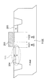
- FIG. 1 is a diagram illustrating an example of a pixel circuit including four transistors in one unit pixel.
- the unit pixel circuit PX1 includes a photodiode 1, a transfer transistor 2, a reset transistor 3, an amplifier transistor 4, a row selection transistor 5, a storage node 6, and a floating diffusion (FD: Floating Diffusion).
- the gate electrode of the transfer transistor 2 is connected to the transfer line 8
- the gate electrode of the reset transistor 3 is connected to the reset line 9.
- the gate electrode of the amplifier transistor 4 is connected to the FD 7, and the gate electrode of the row selection transistor 5 is connected to the row selection line 10.
- the source of the row selection transistor 5 is connected to the vertical signal line 11.
- a constant current circuit 12 and a sensing circuit 13 are connected to the vertical signal line 11.
- the light incident on the silicon substrate of the pixel generates a pair of electrons and holes, and the electrons in the light are condensed and accumulated on the node 6 by the photodiode 1.
- the electrons are finally read out as a signal to the vertical signal line 11.
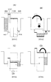
- FIG. 2A to 2D are timing charts of the pixel circuit in FIG.
- the pixel Prior to charge accumulation, the pixel is first reset. This sets the reset line 9 and the transfer line 8 to the high level, and turns on the reset transistor 3 and the transfer transistor 2. This is an operation for transmitting a power supply voltage of 3 V to the storage node 6 of the photodiode, for example. As a result, the potential of the storage node 6 rises and the electrons stored therein are extracted.
- HAD Hole-Accumulation In the (diode) structure, the storage node 6 is formed of an n-type buried diffusion layer sandwiched between p-type layers, and all of its electrons are discharged to be in a fully depleted state.
- the transfer line 8 is set to a low level and the transfer transistor 2 is turned off, whereby the storage node 6 enters a floating state, and a new charge accumulation is started.
- the reset transistor 3 is also normally turned off. In general, such a pixel reset operation is used as an electronic shutter operation of a CMOS image sensor.
- the row selection line 10 becomes high level, the row selection transistor 5 is turned on, and the amplifier transistor 4 of the pixel is connected to the vertical signal line 11.
- the vertical signal line 11 connected to the amplifier transistor 4 and the constant current circuit 12 forms a source follower circuit, and the potential Vf of the FD 7 that is the input and the potential Vsl of the vertical signal line 11 that is the output are:
- the variation ratio is a linear relationship close to 1. That is, when the current value of the constant current circuit 12 is i, the following equation is ideally established.
- Vf ⁇ Vth ⁇ Vsl is constant, and fluctuations in Vf are reflected linearly in Vsl. That is, the source follower circuit operates as an amplifier circuit having a gain of approximately 1, and drives the vertical signal line 11 in accordance with the signal amount of the FD 7 that is an input node.
- the power supply voltage 3V is transmitted to the FD 7 by setting the reset line 9 to the high level and turning on the reset transistor 3. Further, after the reset transistor 3 is turned off, the first sensing of the potential Vsl of the vertical signal line 11 is performed by the sensing circuit 13 constituted by a comparator, an AD converter, or the like. This is readout of the reset signal.
- the transfer line 8 is set to the high level to turn on the transfer transistor 2, whereby electrons stored in the storage node 6 flow into the FD 7.
- the transfer transistor 2 is turned off, and the sensing circuit 13 senses the potential of the vertical signal line 11 for the second time. This is readout of the accumulated signal.
- the difference between the first sensing and the second sensing of Vsl accurately reflects the amount of charge accumulated in the accumulation node 6 by the exposure of the photodiode 1.
- the CMOS imager digitizes this difference and outputs it as a pixel signal value.
- the electron accumulation time of each pixel is a period between the reset operation and the readout operation, and more precisely, is a period T1 from when the transfer transistor 2 is turned off after reset to when it is turned off by readout.
- the accumulated electrons generated by the photoelectric conversion element are converted into an analog signal of the vertical signal line 11 via the amplifier circuit for each pixel and transmitted to the sensing circuit 13. Further, this analog signal is converted into a digital signal by an AD converter and output outside the chip. This is in sharp contrast with a CCD imager in which the stored electrons themselves are vertically and horizontally transferred by CCD transfer until just before the chip output amplifier circuit.
- the potential after transfer of the FD 7 that is the input node of the amplifier circuit 118 is maintained at a higher potential than the photodiode 1 at the time of complete depletion. Need to be drunk.
- the saturated accumulated charge amount Qs of the photodiode corresponds to the number of donors in the diffusion layer, normally, when the saturated accumulated charge amount Qs is increased, the potential at the time of complete depletion becomes deep (high potential). This is in the direction of further narrowing the range of the potential change amount ⁇ Vf.
- Such a transfer margin problem has been a major design limitation.
- An object of the present invention is to provide a pixel circuit, a solid-state imaging device, and a camera system that can facilitate charge transfer in a pixel, improve the amount of stored charge, improve sensitivity, and improve imaging performance. .
- a pixel circuit includes a photoelectric conversion element, an amplifier circuit, and a transfer transistor capable of transferring charges generated by the photoelectric conversion element to an input node of the amplifier circuit,
- the transfer transistor includes first, second, and third field effect transistors that are integrated and connected in series from the photoelectric conversion element toward the amplifier circuit, and the first and second field effect transistors.
- the gate electrode is driven simultaneously and collectively, the threshold voltage of the first field effect transistor is set higher than the threshold voltage of the second field effect transistor, and with the stepwise driving of the gate electrode, The charge generated by the photoelectric conversion element and transferred via the first field effect transistor is accumulated in the channel region of the second field effect transistor, and the channel The charge accumulated in the region to transfer to the input of the amplifier circuit via the third field effect transistor, the amplifier circuit drives a signal line, reading the accumulated charge is performed.
- a pixel circuit includes a photoelectric conversion element, an amplifier circuit, and a transfer transistor capable of transferring charges generated by the photoelectric conversion element to an input node of the amplifier circuit
- the transfer transistor includes first and second field effect transistors that are integrated and connected in series from the photoelectric conversion element toward the amplifier circuit, and the first and second field effect transistors include gates
- the electrodes are driven simultaneously and the threshold voltage of the first field effect transistor is set to be higher than the threshold voltage of the second field effect transistor.
- a predetermined amount of charge generated and transferred through the first field effect transistor is accumulated in the channel region of the second field effect transistor, and the channel Transfers the charge accumulated in the region to the input of the amplifier circuit, the amplifier circuit drives a signal line, reading the accumulated charge is performed.
- a solid-state imaging device includes a pixel unit in which a plurality of pixel circuits are arranged, and a pixel driving unit that drives the pixel circuit of the pixel unit to read out a pixel signal,
- Each pixel circuit includes a photoelectric conversion element, an amplifier circuit, and a transfer transistor capable of transferring charges generated by the photoelectric conversion element to an input node of the amplifier circuit, and the transfer transistor includes the photoelectric conversion element.
- the first and second field effect transistors have gate electrodes
- the threshold voltage of the first field effect transistor is set to be higher than the threshold voltage of the second field effect transistor, and the gate electrode is driven stepwise by the pixel driver. Accordingly, the charge generated by the photoelectric conversion element and transferred through the first field effect transistor is stored in the channel region of the second field effect transistor, and the charge stored in the channel region is stored in the channel region.
- the signal is transferred to the input of the amplifier circuit via the third field effect transistor, and the amplifier circuit drives the signal line to read out the accumulated charge.
- a solid-state imaging device includes a pixel unit in which a plurality of pixel circuits are arranged, and a pixel driving unit that drives the pixel circuit of the pixel unit and reads out a pixel signal.
- Each pixel circuit includes a photoelectric conversion element, an amplifier circuit, and a transfer transistor capable of transferring charges generated by the photoelectric conversion element to an input node of the amplifier circuit, and the transfer transistor includes the photoelectric conversion element.
- the first and second field effect transistors are integrated and connected in series from the conversion element toward the amplifier circuit, and the gate electrodes of the first and second field effect transistors are simultaneously and collectively connected.
- the threshold voltage of the first field-effect transistor is set higher than the threshold voltage of the second field-effect transistor, and the gate electrode is gradually driven by the pixel driver.
- a predetermined amount of charge generated by the photoelectric conversion element and transferred through the first field effect transistor is accumulated in the channel region of the second field effect transistor, and the charge accumulated in the channel region is amplified
- the signal is transferred to the input of the circuit, and the amplifier circuit drives the signal line to read out the accumulated charge.
- a camera system includes a solid-state imaging device, an optical system that forms a subject image on the imaging device, and a signal processing circuit that processes an output image signal of the imaging device
- the solid-state imaging device includes a pixel unit in which a plurality of pixel circuits are arranged, and a pixel driving unit that drives the pixel circuit of the pixel unit and reads out a pixel signal.
- the first, second, and third field effect transistors that are integrated and connected in series, the gate electrodes of the first and second field effect transistors being simultaneously and collectively driven, Up
- the threshold voltage of the first field effect transistor is set higher than the threshold voltage of the second field effect transistor, and is generated by the photoelectric conversion element in accordance with the stepwise driving of the gate electrode by the pixel driver,
- the charge transferred via one field effect transistor is accumulated in the channel region of the second field effect transistor, and the charge accumulated in the channel region is input to the amplifier circuit via the third field effect transistor. Then, the amplifier circuit drives the signal line to read out the accumulated charge.
- a camera system includes a solid-state imaging device, an optical system that forms a subject image on the imaging device, and a signal processing circuit that processes an output image signal of the imaging device
- the solid-state imaging device includes a pixel unit in which a plurality of pixel circuits are arranged, and a pixel driving unit that drives the pixel circuit of the pixel unit and reads out a pixel signal.
- the first and second field effect transistors integrated and connected in series, the gate electrodes of the first and second field effect transistors being simultaneously and collectively driven,
- the threshold voltage of the field effect transistor is set to be higher than the threshold voltage of the second field effect transistor, and is generated by the photoelectric conversion element with the stepwise driving of the gate electrode by the pixel driver, and the first electric field is generated.
- a predetermined amount of charge transferred through the effect transistor is accumulated in the channel region of the second field effect transistor, the charge accumulated in the channel region is transferred to the input of the amplifier circuit, and the amplifier circuit The accumulated charge is read by driving the line.
- charge transfer within a pixel can be facilitated, the amount of accumulated charge and sensitivity can be improved, and imaging performance can be improved.
- FIG. 6 is a diagram illustrating a cross-sectional structure example of the transfer circuit of FIG. 5.
- FIG. 5 is a timing chart when reset, charge accumulation, and readout are performed in the pixel circuit of FIG. 4. It is a figure which shows the equivalent circuit of the transfer circuit containing the transfer transistor of the pixel circuit of FIG. It is a figure which shows the potential transition accompanying the read transfer operation
- FIG. 13 is a timing chart when reset, charge accumulation, and readout are performed in the pixel circuit of FIG. 12. It is a figure which shows the pixel circuit of the CMOS image sensor which concerns on the 4th Embodiment of this invention. It is a figure which shows the timing chart of the operation
- FIG. 20 is a diagram illustrating a timing chart of a pixel operation that adopts an intermediate holding mode and improves the large-capacity accumulation operation of the sixth embodiment in the eighth embodiment. It is a figure which shows the timing chart of the operation
- FIG. 28 is a diagram illustrating a cross-sectional structure example of the transfer circuit of FIG. 27.
- FIG. 16 is a diagram illustrating a configuration example of a transfer circuit according to a fifteenth embodiment in which a photodiode is replaced with a MOS capacitor with respect to FIG. 6 which is a cross-sectional structure example corresponding to the first embodiment. It is a figure which shows the example of a cross-section of the transfer circuit which concerns on 16th Embodiment which has a cross-sectional structure different from the transfer circuit of 1st Embodiment. It is a figure which shows an example of a structure of the camera system with which the solid-state image sensor which concerns on embodiment of this invention is applied.
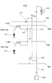
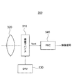
- FIG. 3 is a diagram showing a configuration example of a CMOS image sensor (solid-state imaging device) employing the pixel circuit according to the embodiment of the present invention.
- CMOS image sensor solid-state imaging device
- the present CMOS image sensor 100 includes a pixel array unit 110, a row selection circuit (Vdec) 120 as a pixel driving unit, and a column readout circuit (AFE) 130.
- Vdec row selection circuit
- AFE column readout circuit
- a plurality of pixel circuits 110A are arranged in a two-dimensional shape (matrix shape) of M rows ⁇ N columns.
- the pixel circuit 110A basically includes a photoelectric conversion element, a transfer transistor, a reset transistor, an amplifier transistor, a row selection transistor, a storage node, and an FD (floating diffusion).
- the transfer transistor of the pixel circuit 110A is formed of at least first and second insulated gate field effect transistors (MOS transistors) that are integrated and connected in series, as will be described in detail later.
- the first and second MOS transistors are formed as a high threshold voltage Vth transistor and a low threshold voltage Vth transistor whose gate electrodes are driven simultaneously. A specific configuration of the pixel circuit 110A will be described in detail later.
- a transfer line 140 (LTRG), a reset line 150 (LRST), and a row selection line 160 (LSL) wired to the pixel array unit 110 are wired as a set for each row of the pixel array.
- M control lines are provided for the transfer line 140 (LTRG), the reset line 150 (LRST), and the row selection line 160 (LSL).
- These transfer line 140 (LTRG), reset line 150 (LRST), and row selection line 160 (LSL) are driven by the row selection circuit 120.
- the row selection circuit 120 controls the operation of pixels arranged in an arbitrary row in the pixel array unit 110.
- the row selection circuit 120 controls the pixel circuit through the transfer line 140 (LTRG), the reset line 150 (LRST), and the row selection line 160 (LSL).
- the column readout circuit 130 receives the data of the pixel row controlled to be read out by the row selection circuit 120 through the vertical signal line (LSGN) 170 and transfers it to the signal processing circuit at the subsequent stage.
- a constant current circuit and a sensing circuit are connected to the vertical signal line 170.
- the read circuit 130 includes a CDS circuit and an ADC (analog / digital converter).
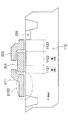
- FIG. 4 is a diagram showing a pixel circuit of the CMOS image sensor according to the first embodiment of the present invention.
- the unit pixel circuit 110A includes a photodiode 111 as a photoelectric conversion element, a transfer transistor 112, a reset transistor 113, an amplifier transistor 114, a row selection transistor 115, a storage node 116, and an FD 117. Note that an amplifier circuit 118 is formed by the amplifier transistor 114, and an input node of the amplifier circuit 118 is formed by the FD 117.
- the transfer transistor 112 of the first embodiment is connected between the photodiode 111 and the FD 117 as an output node.
- the transfer transistor 112 is formed of at least a first MOS transistor 1121, a second MOS transistor 1122, and a third MOS transistor 1123 which are integrated and connected in series.
- the first and second MOS transistors 1121 and 1122 are formed as a transistor having a high threshold voltage Vth and a transistor having a low threshold voltage Vth that are driven by applying a drive signal to the gate electrodes simultaneously.
- the first MOS transistor 1121 is formed as a transistor having a high threshold voltage HVth
- the second MOS transistor 1122 is formed as a transistor having a low threshold voltage LVth.
- the gate electrodes of the first and second MOS transistors 1121 and 1122 are connected in common to the transfer line 140, and the gate electrode of the third MOS transistor 1123 is connected to a reference potential, for example, the ground GND.
- the first, second, and third MOS transistors 1121, 1122, and 1123 are formed as n-channel MOS (NMOS) transistors.
- NMOS n-channel MOS
- the high threshold voltage HVth of the first NMOS transistor 1121 is set to 0V, for example, and the low threshold voltage LVth of the second NMOS transistor 1122 is set to ⁇ 1.5V.
- the threshold voltage of the third MMOS transistor is set to -0.6V.
- the reset transistor 113 is connected between the power supply line and the FD 117, and the regate electrode is connected to the reset line 150.
- the gate of the amplifier transistor 114 is connected to the FD 117.
- the amplifier transistor 114 is connected to the signal line 170 via the row selection transistor 115 and constitutes a constant current circuit 131 outside the pixel portion and a source follower.
- a gate electrode of the row selection transistor 115 is connected to the row selection line 160.
- the source of the row selection transistor 115 is connected to the vertical signal line 170.
- a constant current circuit 131 and a sensing circuit 132 are connected to the vertical signal line 170.
- FIG. 5 is a diagram showing an equivalent circuit of a transfer circuit including the transfer transistor of the pixel circuit 110A according to the first embodiment.
- reference numerals 201 and 202 denote gate electrodes, 203 denotes a parasitic capacitance, and 118 denotes an amplifier circuit.
- the amplifier circuit 118 is formed by an amplifier transistor 114.
- Electrons generated by photoelectric conversion in the photodiode 111 are fed to the FD 117, which is an input node of the amplifier circuit 118, through the first, second, and third NMOS transistors 1121, 1122, and 1123 that are integrated and connected in series. Completely transferred.
- the integrated first, second, and third NMOS transistors 1121, 1122, and 1123 are directly connected to each other without an n-type diffusion layer or the like interposed therebetween.
- the drive signals are applied simultaneously to the gate electrodes 201 of the first and second NMOS transistors 1121 and 1122.
- the first MOS transistor 1121 has a high threshold voltage HVth
- the second MOS transistor 1122 has a low threshold voltage LVth.
- the FD 117 which is an input node, has a parasitic capacitance 203. If the accumulated charge amount is Q and the parasitic capacitance value is Cf, the potential change amount ⁇ Vf is as follows.
- this displacement drives the vertical signal line 170 through the amplifier circuit 118 with a constant gain.
- FIG. 6 is a diagram showing an example of a cross-sectional structure of the transfer circuit of FIG.
- the photodiode 111 employs a so-called HAD structure in which the vicinity of the silicon surface in contact with the oxide film is made p-type.
- the photoelectrically converted electrons are initially stored in the n-type diffusion node 204.
- This diffusion node 204 corresponds to the storage node 116.
- the signal is transferred to the channel region of the second NMOS transistor 1122 via the first NMOS transistor 1121 and stored therein.
- the threshold value of the first NMOS transistor 1121 is set high and the threshold value of the second NMOS transistor 1122 is set low.
- the channel portion CH2 of the second NMOS transistor 1122 forms an electron accumulation well
- the channel portion CH1 of the first NMOS transistor 1121 forms a potential wall for preventing backflow.
- the third NMOS transistor 1123 is controlled by an independent gate electrode 202.
- the potential of the channel region of the third NMOS transistor 1123 is set to be shallower (higher potential) than that of the second NMOS transistor 1122 when an ON voltage is applied to the gate electrode 201.
- the potential of the channel region is set to be deeper (lower potential) than that of the second NMOS transistor 1122 when a voltage for turning off is applied to the gate electrode 201.
- the potential of the gate electrode 202 of the third NMOS transistor 1123 may be fixed. If the impurity profile of the channel portion CH3 of the third NMOS transistor 1123 is appropriately adjusted, it may be connected to a power supply line or a ground line. Is possible.
- the diffusion layer 205 is connected to the input of the amplifier circuit 118 not shown in the cross-sectional view.
- the third NMOS transistor 1123 functions as a separation transistor.
- first NMOS transistor 1121 and the second NMOS transistor 1122 are regarded as two separate transistors here.
- the gate electrode is also integrally formed as shown in the figure, it can be regarded as a single NMOS transistor having a gradient in the impurity profile of the channel portion. In any case, it is functionally similar to two individual transistors connected in series, and the present invention encompasses such a form.
- FIGS. 7A to 7D are diagrams showing potential transitions associated with a read transfer operation using the transfer circuit of the pixel circuit according to the first embodiment.
- each node serves as a well for accumulating negatively charged electrons, and the potential is lifted upward, that is, in the negative potential direction as the well fills with electrons.
- Step ST11 In step ST11 of FIG. 7A, the diffusion node 204 of the photodiode 111 is designed to be positively charged by a certain number of donors and have a potential bottom of about 2.0 V when fully depleted. Here, the photoelectrically converted electrons are filled up to a saturated state (about 0 V).
- the channel regions of the first NMOS transistor 1121 and the second NMOS transistor 1122 are modulated in the range of R11 and R12, respectively, according to the potential applied to both gate electrodes, for example, ⁇ 1.5V to 3V. Is done.
- the gate electrode 202 of the third NMOS transistor 1123 as the isolation transistor is connected to the ground GND, and the channel potential is adjusted to about 0.6V. Further, the diffusion layer 205 (FD 117) which is an input node of the amplifier circuit 118 is reset and is in a floating state of 3V.
- Step ST12 In step ST12 in FIG. 7B, when the first NMOS transistor 1121 and the second NMOS transistor 1122 are turned on, electrons are moved as follows. The electrons accumulated in the diffusion node 204 of the photodiode 111 do not remain through the first NMOS transistor 1121 and move to the channel region of the second NMOS transistor 1122. That is, electrons move to the channel region of the second NMOS transistor 1122 in a deep depletion state, and are accumulated in an analog state.
- the potential of the channel region of the third NMOS transistor 1123 is shallower (lower potential) than that of the second NMOS transistor 1122, and between the diffusion layer 205 (FD 117) that is the input node of the amplifier circuit 118. It forms a barrier.
- Step ST13 In step ST13 of FIG. 7C, when the gate electrode is driven to turn off the first NMOS transistor 1121 and the second NMOS transistor 1122, the potential of the channel region is modulated in the negative potential direction accordingly. Is done.
- the channel of the first NMOS transistor 1121 forms a potential barrier to prevent the backflow of accumulated electrons to the diffusion node 204 of the photodiode 111.
- the height of the barrier corresponds to the difference between the threshold values of the first NMOS transistor 1121 and the second NMOS transistor 1122, and is, for example, 1.5V.
- the gate electrodes 201 of the first and second NMOS transistors 1121 and 1122 reach an appropriate intermediate voltage, the stored electrons are separated from both the diffusion node 204 of the photodiode 111 and the FD 117 which is the input of the amplifier. A condition can arise.
- the gate may be driven all at once until the next step, but a new function can be added by temporarily holding such an intermediate state as will be described later. Further, when the gate is continuously driven from here to modulate the potential of the channel region of the second NMOS transistor 1122 in the negative potential direction, the electrons accumulated therein are diffusion layers 205 ( Start moving to FD117).
- Step ST114 In step ST14 of FIG. 7D, when the first NMOS transistor 1121 and the second NMOS transistor 1122 are completely turned off, the potential of the channel region of the second NMOS transistor 1122 that has released all accumulated electrons is It becomes like this. That is, the channel region potential of the second NMOS transistor 1122 exceeds the channel potential of the third NMOS transistor 1123. Then, all the electrons accumulated in the photodiode 111 in step ST11 are moved to the diffusion layer 205 (FD117) which is an input node of the amplifier circuit 118. As a result, the amplifier circuit 118 drives the vertical signal line 170 to read out the accumulated signal.
- FD117 diffusion layer 205
- stepwise transfer it is not necessary to secure a potential difference between the diffusion node 204 of the photodiode 111 that is in a fully depleted state and the FD 117 that is the input node of the amplifier circuit 118. That is, in this example, complete transfer is realized even if the potential of the FD 117 filled with electrons is shallower than that of the diffusion node 204.
- FIG. 8A to 8D are timing charts when reset, charge accumulation, and readout are performed in the pixel circuit of FIG. 8A shows the signal potential of the reset line 150, FIG. 8B shows the signal potential of the transfer line 140, FIG. 8C shows the signal potential of the row selection line 160, and FIG. 8D shows the vertical potential. Each signal potential of the signal line 170 is shown.
- the characteristic operation of the pixel circuit 110A of the first embodiment is that the transfer of the stored electrons of the photodiode 111 to the FD 117 is performed in two stages corresponding to the drive of the transfer line 140. That is, when the transfer line 140 rises from the low level to the high level, the accumulated electrons are transferred from the diffusion node 204 of the photodiode 111 to the channel region of the second NMOS transistor 1122 as shown in step ST12 of FIG. Transferred. Further, when the transfer line 140 returns from the high level to the low level, the electrons in the channel region are transferred to the FD 117 which is the input node of the amplifier circuit 118, as shown in step ST14 of FIG.
- the FD 117 which is the input node of the amplifier circuit 118 is connected to the reset level potential (power supply voltage ⁇ 3 V).
- the transfer line 140 rises from the low level to the high level and further falls from the high level to the low level, the electrons accumulated in the photodiode 111 are transferred to the diffusion layer 205 and extracted to the reset level.
- a new electron accumulation period T2 starts at this point.
- the reset pulse of the reset line 150 falls to the low level after waiting for the transfer line 140 to fall to the low level.
- the electrons accumulated in the photodiode 111 are transferred to the diffusion layer 205 when the transfer line 140 rises from the low level to the high level and further falls from the high level to the low level. Therefore, the driving of the vertical signal line 170 via the amplifier circuit 118 by the accumulated signal occurs when the transfer line 140 returns from the high level to the low level.
- the accumulation period T2 also ends at this point.
- the pixel circuit 110A it is possible to facilitate the charge transfer in the pixel in the CMOS image sensor, to improve the amount of accumulated charge and the sensitivity, and to improve the imaging performance. Become.
- FIG. 9 is a diagram showing an equivalent circuit of the transfer circuit including the transfer transistor of the pixel circuit PX1 of FIG.
- GT1 represents a gate electrode
- C1 represents a parasitic capacitance
- 8 represents an amplifier circuit.
- the amplifier circuit 14 is formed by the amplifier transistor 4.
- the transfer circuit TX1 electrons generated by photoelectric conversion by the photodiode 1 are accumulated in the accumulation node 6 that is a diffusion layer node of the photodiode 1. At the time of reading, they are completely transferred to the FD 7 that is the input node of the amplifier circuit 14 via the transfer transistor 2.
- an NMOS transistor such as the amplifier transistor 4 is usually used, but a unique random noise Nr is generated. Therefore, when the gain is G, the S / N ratio of the accumulated signal generated in the vertical signal line as an output is ⁇ G ⁇ ⁇ Vf / Nr ⁇ . Since the gain G and random noise Nr are substantially constant once the configuration of the amplifier circuit 14 is determined, the magnitude of the potential change amount ⁇ Vf directly affects the imaging performance.
- FIGS. 10A to 10D are diagrams showing potential transitions associated with the read transfer operation using the pixel circuits as shown in FIGS.
- each node serves as a well for accumulating negatively charged electrons, and the potential is lifted upward, that is, in the negative potential direction as the well fills with electrons.
- Step ST1 In step ST1 of FIG. 10A, the storage node 6 which is the diffusion node of the photodiode 1 is designed to be positively charged by a certain number of donors and have a potential bottom of about 1.5 V when fully depleted. ing. Here, the photoelectrically converted electrons are filled up to a saturated state (about 0 V). On the other hand, the potential of the channel region of transfer transistor 2 is modulated in the range of R1 according to the potential applied to the gate electrode, for example, 1V to 3V. Further, the FD 7 which is an input node of the amplifier circuit 14 is reset and is in a floating state of 3V.
- Step ST2 In step ST2 of FIG. 10B, when the transfer transistor 2 is turned on, electrons move as follows. That is, when the transfer transistor 2 is turned on, the electrons accumulated in the accumulation node 6 that is the diffusion node of the photodiode 1 are not distributed and are distributed to the channel region of the transfer transistor 2 and the FD 7 that is the input node of the amplifier circuit 14. Moving.
- Step ST3 In step ST3 of FIG. 10C, when the potential of the channel region rises as the gate electrode rises in order to turn off the transfer transistor 2, the electrons accumulated therein are the input nodes of the amplifier circuit 14. Move to FD7.
- Step ST4 In step ST4 of FIG. 10D, when the transfer transistor 2 is in an off state, all the electrons accumulated in the photodiode 1 in step ST1 are moved to the FD7 that is the input node of the amplifier circuit. As a result, the amplifier circuit 14 drives the vertical signal line 11 to read out the accumulated signal.
- the pixel circuit PX1 in FIG. 1 is between the storage node 6 of the photodiode 1 in a fully depleted state and the FD7 that is the input node of the amplifier circuit 14. Needs to have a potential difference M1. On the other hand, if this potential difference is not sufficiently secured, electrons accumulated in the channel region of the transfer transistor 2 will flow backward to the photodiode 1 and the amount of electrons accumulated in the photodiode 1 will not be reflected linearly in the read signal.
- the potential after transfer of the FD 7 that is the input node of the amplifier circuit 14 needs to be kept higher than the photodiode 1 at the time of complete depletion. is there.
- the pixel circuit PX1 of FIG. 1 has a disadvantage that the potential dynamic range of the FD 7 is limited, ⁇ Vf cannot be sufficiently increased, and the S / N ratio cannot be increased.
- ⁇ Vf has a limit of (3.0V ⁇ 1.5V), and the potential difference corresponding to the transfer margin is further subtracted.
- the saturation accumulated charge amount Qs of the photodiode 1 corresponds to the number of donors in the diffusion layer. Therefore, when Qs is increased normally, the potential at the time of complete depletion becomes deep (high potential). . This is a direction that further narrows the range of ⁇ Vf. Such a transfer margin problem is a great design limitation.
- the pixel circuit 110A of the first embodiment employs transfer using an integrated series transistor for transferring electrons from the photodiode in the pixel to the amplifier circuit.
- an intermediate transfer node capable of potential modulation is formed in the channel portion of the MOS transistor, and stored electrons are transferred stepwise from the photodiode 111 to the amplifier circuit 118 via the intermediate node. .
- the above-described potential restriction for transfer can be released, thereby increasing the saturation accumulated charge amount Qs or reducing the parasitic capacitance of the amplifier input unit,
- the dynamic range can be improved.
- the pixel circuit 110A stores electrons photoelectrically converted during exposure not in the photodiode but in a channel region of a separately formed MOS transistor, and at the time of reading, completely transfers the stored electrons to the amplifier circuit. Can do. Therefore, according to the pixel circuit 110A, the exposure sensitivity can be improved and the saturated accumulated charge amount Qs can be greatly improved.
- the pixel circuit 110A electron (charge) transfer is performed only within the pixel, and after the vertical signal line is driven by the amplifier circuit, a low-impedance analog signal or digital signal is transmitted. Therefore, it is possible to realize a high-speed and low power consumption imager without problems of M smear and transfer leakage.
- FIG. 11 is a diagram showing a pixel circuit of a CMOS image sensor according to the second embodiment of the present invention.
- the pixel circuit 110B according to the second embodiment is different from the pixel circuit 110A according to the first embodiment as follows.
- a plurality of, for example, two pixels PXL110a and PXL110b each having a unique photodiode 111 and transfer circuit 112 share an FD 117 and an amplifier transistor 114 that form an amplifier circuit.
- the reset transistor 113 and the row selection transistor 115 are also shared by the plurality of pixels PXL110a and PXL110b.
- the shared gate electrodes of the first and second NMOS transistors are connected to different transfer lines 140a and 140b, respectively.
- the gate electrodes of the third MOS transistors 1123 of the transfer transistors 112a and 112b of the pixels PXL110a and PXL110b are respectively grounded.
- the electrons accumulated in the photodiodes 111a and 111b are transferred to the FDF 117 (input node of the amplifier circuit) at individual timings according to the independent transfer lines 140a and 140b.
- Sharing the amplifier circuit can reduce the effective size of the pixel, but the parasitic capacity of the FD 117 increases as the number of shared pixels increases. Therefore, the number of shared pixels is desirably 2 pixels or more and 16 pixels or less.
- FIG. 12 is a diagram showing a pixel circuit of a CMOS image sensor according to the third embodiment of the present invention.
- the pixel circuit 110C according to the third embodiment is different from the pixel circuit 110A according to the first embodiment as follows.
- the gate electrode 202 of the third NMOS transistor 1123 which was set to the fixed potential in the first embodiment, is driven by the row selection circuit 120 that is a peripheral circuit.
- the shared gate electrode 201 of the first and second NMOS transistors 1121 and 1122 is connected to the first transfer line 141, and the gate electrode 202 of the third NMOS transistor 1123 is connected to the second transfer line (distribution). (Separated line) 142.
- FIGS. 13A to 13D are diagrams showing potential transitions associated with a read transfer operation using the pixel circuit 110C according to the third embodiment.
- Step ST21 In step ST21 in FIG. 13A, the diffusion node 204 of the photodiode 111 is designed to be positively charged by a certain number of donors and have a potential bottom of about 2.0 V when fully depleted. Here, the photoelectrically converted electrons are filled up to a saturated state (about 0 V).
- the channel regions of the first NMOS transistor 1121 and the second NMOS transistor 1122 are modulated in the range of R13 and R14, respectively, in accordance with the potential applied to both gate electrodes, for example, ⁇ 0.5V to 3V. Is done.
- the potential of the channel region of the third NMOS transistor 1123 as the isolation transistor is modulated in the range of R15 according to the potential inherent to the gate electrode, for example, 0V to 3V.
- the diffusion layer 205 (FD 117) which is an input node of the amplifier circuit 118 is reset and is in a floating state of 3V.
- Step ST22 In step ST22 of FIG. 13B, when the first NMOS transistor 1121 and the second NMOS transistor 1122 are turned on, the electron transfer is performed as follows. That is, the electrons accumulated in the diffusion node 204 of the photodiode 111 do not remain through the first NMOS transistor 1121 and move to the channel region of the second NMOS transistor 1122. That is, electrons move to the channel region of the second NMOS transistor 1122 in a deep depletion state, and are accumulated in an analog state.
- the potential of the channel region of the third NMOS transistor 1123 is secondly shallower (lower potential) than that of the NMOS transistor 1122, and between the diffusion layer 205 (FD 117) that is the input node of the amplifier circuit 118. It forms a barrier.
- Step ST23 In step ST23 of FIG. 13C, when the first NMOS transistor 1121 and the second NMOS transistor 1122 are turned off again, the potential of the channel region is modulated in the negative potential direction.
- the channel of the first NMOS transistor 1121 forms a potential barrier to prevent the backflow of accumulated electrons to the diffusion node 204 of the photodiode 111.
- the height of the barrier corresponds to the difference between the threshold values of the first NMOS transistor 1121 and the second NMOS transistor 1122, and is, for example, 1.5V.
- Step ST24 In step ST24 of FIG. 13D, when the gate electrode 203 of the third NMOS transistor 1123 is driven through the second transfer line 142 as a separation line and the third NMOS transistor 1123 is turned on, the stored electrons are amplified. It flows into the FD 117 which is an input node of the circuit 118. Further, when the third NMOS transistor 1123 is turned off, all the stored electrons are moved to the diffusion layer 205 (FD 117) which is an input node of the amplifier circuit 118. As a result, the amplifier drives the vertical signal line, and the stored signal is read out.
- the transfer from the channel of the second NMOS transistor 1122 in the third embodiment to the FD 117 that is the input node of the amplifier circuit 118 is performed as follows.
- stepwise transfer it is not necessary to secure a potential difference between the diffusion node 204 of the photodiode 111 that is in a fully depleted state and the FD 117 that is the input node of the amplifier circuit 118. That is, in this example, complete transfer is realized even if the potential of the FD 117 filled with electrons is shallower than that of the diffusion node 204.
- FIG. 14A to 14E are timing charts when reset, charge accumulation, and readout are performed in the pixel circuit of FIG. 14A shows the signal potential of the reset line 150, FIG. 14B shows the signal potential of the first transfer line 141, and FIG. 14C shows the signal potential of the second transfer line (separation line) 142. Respectively. 14D shows the signal potential of the row selection line 160, and FIG. 14E shows the signal potential of the vertical signal line 170.
- the diffusion node 204 of the photodiode 111 moves from the diffusion node 204 to the channel region of the second NMOS transistor 1122 as shown in step ST22 of FIG.
- Stored electrons are transferred.
- the first transfer line 141 returns from the high level to the low level and the second transfer line 142 as the separation line becomes the high level almost simultaneously with the first transfer line 141, the following electron movement is performed.
- the third NMOS transistor 1123 is turned on as a separation transistor, and stored electrons flow into the FD 117 which is an input node of the amplifier circuit 118.
- the second transfer line 142 as the separation line falls to a low level, complete transfer to the FD 117 that is the input node of the electronic amplifier circuit 118 is completed.
- the FD 117 which is an input node of the amplifier circuit is connected to the reset level potential (power supply voltage ⁇ 3 V).
- the first transfer line 141 rises from the low level to the high level, excess electrons accumulated in the photodiode 111 pass through the first NMOS transistor 1121 and the channel portion CH2 of the second NMOS transistor 1122.
- the first transfer line 141 falls from the high level to the low level, and at the same time, the second transfer line 142 becomes the high level as the separation line, and the third NMOS transistor 1123 as the separation transistor becomes conductive.
- T3 starts when the first transfer line 141 falls from the high level to the low level.
- the electrons accumulated in the photodiode 111 are first increased from the low level to the high level by the first transfer line 141, so that the second MOS transistor 1122 is passed through the first NMOS transistor 1121.
- the first transfer line 141 falls from the high level to the low level, and the second transfer line 142 as the separation line rises to the high level substantially at the same time, and finally falls to the low level, they are amplified. Is completely transferred to the FD 117, which is the input node of.
- the accumulation period T3 ends at this point.
- the timing at which the second transfer line 142 as the separation line is turned on may be before or after the timing at which the first transfer line 141 is turned off.
- the amplifier transistor 114 is turned on through the FD 117 before the level at which the first transfer line 141 is turned off, the state from step ST22 in FIG. 13B to step ST23 in FIG. 13C is skipped. The process proceeds to step ST24 of D).
- complete transfer can be realized as long as the second transfer line 142 as the separation line is turned off after the first transfer line 141 is turned off.
- FIG. 15 is a diagram showing a pixel circuit of a CMOS image sensor according to the fourth embodiment of the present invention.
- the pixel circuit 110D according to the fourth embodiment is different from the pixel circuit 110C according to the third embodiment as follows.
- a plurality of, for example, two pixels PXL110a and PXL110b each having a unique photodiode 111 and transfer circuit 112 share an FD 117 and an amplifier transistor 114 that form an amplifier circuit.
- the reset transistor 113 and the row selection transistor 115 are also shared by the plurality of pixels PXL110a and PXL110b.
- the transfer transistors 112a and 112b of the respective pixels PXL110a and PXL110b are connected to first transfer lines 1410a and 141b having different shared gate electrodes of the first and second NMOS transistors, respectively.
- the gate electrodes of the third MOS transistors 1123 of the transfer transistors 112a and 112b of the pixels PXL110a and PXL110b are respectively connected to second transfer lines 142a and 142b serving as separation lines.
- the electrons accumulated in the photodiodes 111a and 111b are FDF117 at individual timings according to the first transfer lines 141a and 141b that are independent from each other and the second transfer lines 142a and 142b as the separation lines. Forwarded to
- Sharing the amplifier circuit can reduce the effective size of the pixel, but the parasitic capacity of the FD 117 increases as the number of shared pixels increases. Therefore, the number of shared pixels is desirably 2 pixels or more and 16 pixels or less.
- the large-capacity storage operation can be applied to any of the circuit configurations of the first to fourth embodiments described above, and will be described below as fifth and sixth embodiments, respectively.
- the pixel circuit configuration of FIG. 4 employed in the first embodiment and the charge accumulation using the deep depletion state of the second NMOS transistor 1122 are applied. Specifically, electrons accumulated in the diffusion node 204 that is the diffusion layer of the photodiode 111 are transferred to the channel portion of the second NMOS transistor 1122 and accumulated during the accumulation period. That is, during the pixel accumulation period, the gate electrode 201 is maintained at the on-state level so that the first and second NMOS transistors 1121 and 1122 are maintained in the on-state.
- the electrons photoelectrically converted by the photodiode 111 are immediately transferred to the channel portion CH2 of the second NMOS transistor 1122 via the first NMOS transistor 1121 and stored therein.
- the gate electrode 201 is driven so that the first and second NMOS transistors 1121 and 1122 are turned off.
- the accumulated electrons are transferred to the FD 117 that is the input node of the amplifier circuit 118 via the third NMOS transistor 1123.
- FIGS. 16A to 16D are timing charts showing the operation of the fifth embodiment.
- 16A shows the signal potential of the reset line 150
- FIG. 16B shows the signal potential of the transfer line 140
- FIG. 16C shows the signal potential of the row selection line 160
- FIG. Each signal potential of the signal line 170 is shown.
- the pixel circuit is the same as that shown in FIG. 4, and the details and cross-sectional configuration of the transfer circuit are the same as those shown in FIGS.
- the transfer line 140 is again in the high level state and is maintained in the high level state during the accumulation period T4. .
- the electrons photoelectrically converted by the photodiode 111 are not accumulated in the diffusion layer but immediately transferred to the channel region of the second NMOS transistor 1122 and accumulated there.
- the row selection line 160 becomes high level, and the output of the amplifier circuit is connected to the vertical signal line 170. Further, the FD 117 that is the input node (8c) of the amplifier circuit 118 is reset by a pulse to the reset line 150, and the FD 117 is connected to the power supply voltage source, whereby the reset level is read. Next, the transfer line 140 transitions from a high level to a low level. As a result, electrons accumulated in the channel region of the second NMOS transistor 1122 are transferred to the FD 117, which is an input node of the amplifier circuit 118, and the accumulated signal is read. The accumulation period T4 also ends with the transition of the transfer line 140.
- the potential transition of the embodiment of the present invention is in accordance with FIGS. 7A to 7D.
- the state is not step ST11 in FIG. 7A but the state in step ST12 in FIG. 7B. Yes.
- the first NMOS transistor 1121 and the second NMOS transistor 1122 are kept on.
- the electrons photoelectrically converted by the photodiode 111 and collected in the diffusion node 204 immediately move to the channel region of the second NMOS transistor 1122 via the first NMOS transistor 1121. That is, electrons move to the channel region of the second NMOS transistor 1122 in a deep depletion state, and are accumulated in an analog state. Transfer of electrons from the second NMOS transistor 1122 to the diffusion layer 205 at the time of reading is the same as the steps ST13 and ST14 in FIGS. 7C and 7D.
- the photodiode 111 is always kept in the same fully depleted state. Therefore, the sensitivity and the linearity between the accumulation time and the accumulation signal are also improved.
- the sensitivity and the linearity between the accumulation time and the accumulation signal are also improved.
- holes generated in the depletion layer are attracted to the internal electric field and quickly discharged to the substrate.
- the internal electric field is reduced accordingly, the hole discharging ability is lowered, and recombination of electrons and holes is likely to occur.
- the sensitivity gradually decreases. On the other hand, such a problem does not occur in the fifth embodiment.
- the saturation accumulated charge amount of the photodiode itself is small, it does not cause a problem. Therefore, it is possible to reduce the irregularity concentration of the diffusion layer and suppress the generation of dark current and white spots.
- the potential formed in the diffusion node 204 of the photodiode 111 at the time of reset can be made shallower. Therefore, the modulation ranges R11 and R12 of the channel regions of the first NMOS transistor 1121 and the second NMOS transistor 1122 can be reduced, and it is easy to ensure reliability such as withstand voltage.
- the fifth embodiment of the present invention it is possible to improve all of the basic performances of the image sensor, such as the amount of accumulated charge, sensitivity, and white point.
- FIG. 17A shows the signal potential of the reset line 150
- FIG. 17B shows the signal potential of the first transfer line 141
- FIG. 17C shows the signal potential of the second transfer line (separation line) 142
- Respectively. 17D shows the signal potential of the row selection line 160
- FIG. 17E shows the signal potential of the vertical signal line 170.
- the pixel circuit is the same as that shown in FIG. 12, and the transition of the transfer potential is the same as that shown in FIGS.
- the first transfer line 141 again becomes a high level state, and maintains the high level state during the accumulation period T5. Yes.
- the electrons photoelectrically converted by the photodiode 111 are not accumulated in the diffusion layer but immediately transferred to the channel region of the second NMOS transistor 1122 and accumulated there. That is, the state of step ST22 in FIG. 13B in the potential diagram is maintained.
- the row selection line 160 becomes high level, and the output of the amplifier circuit 118 is connected to the vertical signal line 170.
- the reset level 150 is read by resetting the FD 117, which is the input node of the amplifier circuit 118, to the power supply voltage source by a pulse to the reset line 150.
- the first transfer line 141 changes from a high level to a low level, and a pulse is also applied to the second transfer line 142 as a separation line.
- the accumulation period T5 also ends with the transition of the first transfer line 141.
- the state is as follows in the intermediate state of step ST13.
- the electrons accumulated in the channel region of the second NMOS transistor 1122 as the intermediate accumulation node are separated from the diffusion node 204 of the photodiode 111 and the FD 117 as the amplifier input. That is, electrons newly photoelectrically converted at the diffusion node 204 of the photodiode 111 do not flow into the intermediate storage node, and electrons stored at the intermediate storage node do not flow into the FD 117.
- the shared gates of the first and second NMOS transistors 1121 and 1122 are driven with three values, and such a state is realized by the intermediate voltage, thereby maintaining this intermediate state for a certain period. Is possible.
- the following is performed in the intermediate state of step ST23.
- the electrons accumulated in the channel region of the second NMOS transistor 1122 as the intermediate accumulation node are separated from the diffusion node 204 of the photodiode 111 and the FD 117 as the amplifier input.
- the intermediate state can be maintained for a certain period by turning off the first and second NMOS transistors 1121 and 1122 and the third NMOS transistor 1123 by driving the gate electrode.
- the certain period is, for example, a period longer than the minimum accumulation period, or a period longer than the period required for reading one row.
- 18A to 18D are timing charts of pixel operations in which the intermediate holding mode is employed in the seventh embodiment and the large-capacity accumulation operation of the fifth embodiment is improved.
- 18A shows the signal potential of the reset line 150
- FIG. 18B shows the signal potential of the transfer line 140
- FIG. 18C shows the signal potential of the row selection line 160
- FIG. Each signal potential of the signal line 170 is shown.
- the pixel circuit is the same as that shown in FIG. 4, and the details and cross-sectional configuration of the transfer circuit are the same as those shown in FIGS.
- the seventh embodiment which is an improved example, increases the dark current by driving the gate electrode 201 and turning on the first and second NMOS transistors 1121 and 1122 intermittently. Is suppressed. That is, first, a reset operation similar to that in FIGS. 8 and 16 is performed to start a new accumulation.
- the first and second NMOS transistors 1121 and 1122 are not kept open through the gate electrode 201, but are intermittently set to the high level so as to be time-shared from the photodiode 111 to the intermediate accumulation node.
- the electron is being transferred.
- the gate electrode 201 is maintained at the intermediate potential, and the intermediate storage node maintains the intermediate state of step ST13 in FIG. 7C.
- the gate electrode 201 is again set to the high level, and the electrons remaining in the photodiode 111 are transferred to the intermediate storage node.
- the gate electrode 201 is set to the low level, and the electrons stored in the intermediate storage node are collectively transferred to the FD 117 as the amplifier input.
- FIGS. 19A to 19E show pixel operations in the eighth embodiment in which the intermediate holding mode is adopted based on the same concept as in the seventh embodiment, and the large capacity storage operation of the sixth embodiment is improved. It is a figure which shows a timing chart.
- FIG. 19A shows the signal potential of the reset line 150
- FIG. 19B shows the signal potential of the first transfer line 141
- FIG. 19C shows the signal potential of the second transfer line (separation line) 142
- Respectively. 19D shows the signal potential of the row selection line 160
- FIG. 19E shows the signal potential of the vertical signal line 170.
- the pixel circuit is the same as that shown in FIG. 12, and the transition of the transfer potential is the same as that shown in FIGS.
- the same reset as in FIG. 14 and FIG. 17 is performed to start a new accumulation.
- the first and second NMOS transistors 1121 and 1122 driven by the gate electrode 201 are not kept open, but pulses are intermittently applied to the intermediate accumulation node from the photodiode 111. Electrons are transferred in time division.
- the third NMOS transistor 1123 is kept off through the isolation gate electrode 202, and the intermediate accumulation node other than the intermittent transfer is maintained at the intermediate state in step ST23 of FIG. 13C. ing.
- a pulse is again applied to the gate electrode 201 to turn on the first and second NMOS transistors 1121 and 1122, and the electrons remaining in the photodiode 111 are transferred to the intermediate storage node.
- a pulse is applied to the separation gate electrode 202 to turn on the third NMOS transistor 1123, and the accumulated electrons at the intermediate accumulation node are collectively transferred to the FD 117 which is an amplifier input.
- an increase in dark current can be suppressed while realizing a large capacity accumulation as in the seventh embodiment.
- the global shutter function is a function that removes so-called focal plane distortion that has occurred due to a shift in shutter timing within the pixel array.
- the start of the read operation determines the accumulation end timing. Since reading is performed sequentially for each normal row, the accumulation end timing also follows that. Therefore, usually, a reset operation for starting accumulation is also sequentially performed by shifting for each row, and measures are taken to make the accumulation period T1 uniform for all effective pixels.
- This is called a rolling shutter and is a common technique in CMOS image sensors, but means that the shutter timing is shifted for each row, and for example, distortion occurs in an image of a subject that operates at high speed.
- the global shutter function is realized by simultaneously starting the charge accumulation of all effective pixels and ending the accumulation simultaneously.
- the accumulation data is read out for each row, in this case, it is necessary to separate the accumulation end and the read timing, and it is necessary to store a signal for each pixel during the period from the end of accumulation to the readout.
- the configuration of the transfer circuit shown in FIG. 5 is used and the intermediate holding mode is used, such an operation and good signal storage are possible. That is, in the CMOS image sensor 100, the first and second NMOS transistors 1121 and 1122 are turned off simultaneously through the gate electrode 201 for all effective pixels. Accordingly, the transfer of the photoelectrically converted electrons is stopped to complete the accumulation, and the already accumulated electrons are temporarily stored in the channel region of the second NMOS transistor 1122. After that, when reading is performed in units of rows, a pulse is given to the gate electrode 202 to sequentially turn on the third NMOS transistor 1123, and the stored electrons are transferred to the FD 117 which is the input node of the amplifier circuit 118. good.
- FIGS. 20A to 20D are timing charts showing operations in the ninth embodiment in which the global shutter function is installed in the first embodiment.
- 20A shows the signal potential of the reset line 150
- FIG. 20B shows the signal potential of the transfer line 140
- FIG. 20C shows the signal potential of the row selection line 160
- FIG. Each signal potential of the signal line 170 is shown.
- the pixel circuit conforms to FIG. 4, and the potential transition conforms to FIG.
- the FD 117 which is an input node of the amplifier circuit 118 is connected to the reset level (power supply voltage ⁇ 3V).
- the transfer line 140 rises from the low level to the high level and further falls from the high level to the low level, the electrons accumulated in the photodiode 111 are transferred to the FD 117 and extracted to the reset level.
- a new electron accumulation period T8 starts at this point.
- the pulse of the reset line 150 falls to the low level after waiting for the pulse applied to the gate electrode 201 to fall to the low level. Normally, this reset operation is performed sequentially for each selected row, but in a global reset, it is performed simultaneously for all effective pixels. That is, this step is a global shutter opening operation.
- the electrons accumulated in the photodiode 111 are first transferred to the intermediate accumulation node by the transfer line 140 rising from the low level to the high level.
- the potential state at this time corresponds to step ST12 in FIG.
- the transfer line 140 returns from the high level to the intermediate potential, the potential state shifts to the intermediate holding mode in step ST13 in FIG. 7B, and the intermediate storage node and the photodiode 111 are disconnected.
- Reading is sequentially performed for each row along the row address.
- a selection signal is applied to the row selection line 160 to selectively perform row selection
- a pulse is applied to the reset line 150, and the FD 117, which is an amplifier input unit, is connected to the reset level so that the reset level is set. Perceived.
- the transfer line 140 falls from the intermediate potential to the low level state, whereby all the electrons held in the intermediate storage node are transferred to the FD 117 that is the input node of the amplifier circuit 118.
- Each pixel maintains the intermediate holding mode for a period of H8 from the end of accumulation to reading, but the intermediate holding period H8 is different for each row. In other words, the intermediate holding is performed for a period from when the shutters are closed all the time until the reading order is turned to the corresponding row.
- FIGS. 21A to 21E are timing charts showing the operation of the tenth embodiment in which the global shutter function is installed in the third embodiment.
- FIG. 21A shows the signal potential of the reset line 150
- FIG. 21B shows the signal potential of the first transfer line 141
- FIG. 21C shows the signal potential of the second transfer line (separation line) 142
- Respectively. 21D shows the signal potential of the row selection line 160
- FIG. 21E shows the signal potential of the vertical signal line 170.
- the pixel circuit is the same as that in FIG. 12, and the transition of the transfer potential is the same as in FIGS. 13A to 13D.
- the FD 117 which is an input node of the amplifier circuit 118 is connected to the reset level (power supply voltage ⁇ 3V).
- the first transfer line 141 rises from the low level to the high level, excess electrons accumulated in the photodiode 111 are transferred to the channel portion of the second NMOS transistor 1122 via the first NMOS transistor 1121. Transferred. Further, the first transfer line 141 falls from the high level to the low level, and at the same time, the second transfer line 142 as the separation line becomes the high level, and the separation third NMOS transistor 1123 becomes conductive.
- the electrons accumulated in the photodiode 111 are first transferred to the intermediate accumulation node by the first transfer line 141 rising from the low level to the high level.
- the potential state at this time corresponds to step ST22 in FIG.
- the potential state shifts to the intermediate holding mode in step ST23 in FIG. 13B, and the intermediate storage node and the photodiode are disconnected.
- Reading is sequentially performed for each row along the row address.
- a selection signal is applied to the row selection line 160 to selectively perform row selection
- a pulse is applied to the reset line 150, and the FD 117 portion which is an input node of the amplifier circuit 118 is connected to the reset level.
- the reset level is detected.
- the second transfer line 142 as a separation line is driven to a high level, and the third NMOS transistor 1123 which is a separation transistor is turned on. As a result, electrons accumulated in the channel portion of the second NMOS transistor 1122 are transferred to the FD 117 which is an input node of the amplifier 118.
- each pixel maintains the intermediate holding mode for a period of H9 from the end of accumulation to reading, but the intermediate holding period H9 is different for each row. In other words, the intermediate holding is performed for a period from when the shutters are closed all the time until the reading order is turned to the corresponding row.
- the global shutter function can be executed in combination with the above-described large-capacity storage operation. For example, when accumulation of the global shutter sequence shown in FIGS. 20A to 20D is started, the transfer lines 140 of all effective pixels are collectively changed to the high level. Then, after maintaining the state during the accumulation period T8, the accumulation is ended by dropping it to the intermediate potential in a lump, and the state is shifted to the intermediate holding state. In this case, during the accumulation period, the potential state of step ST12 in FIG. 7B is maintained in each pixel, and electrons are accumulated not in the photodiode 111 but in the channel of the second NMOS transistor 1122, thereby accumulating large capacity. Is possible.
- Both the basic configuration of the first embodiment and the basic configuration of the third embodiment are used in combination with a large-capacity accumulation operation and a global shutter function. can do.
- This function stores a short accumulation time signal and a long accumulation signal in one pixel at the same time, and uses a short accumulation time signal for high-luminance object sensing and a long accumulation time signal for low-luminance object sensing. Thus, it is a function of capturing both images simultaneously with an appropriate exposure time.
- a signal accumulated for a long time in the same pixel is stored in the channel region of the transistor in the intermediate holding mode, and photo A separate signal can be stored in the diode.
- the long-time accumulation side signal stored in the intermediate holding mode is transferred to the amplifier input, and then the short-time accumulation side signal held in the photodiode is transferred.
- FIGS. 22 (A) to (D) and FIGS. 23 (A) to (C) An example of a wide dynamic range operation using the configuration of the first embodiment will be described using the potential transition diagrams of FIGS. 22 (A) to (D) and FIGS. 23 (A) to (C).
- 22A to 22D are first potential transition diagrams for explaining an example of the wide dynamic range operation in the eleventh embodiment using the configuration of the first embodiment.
- FIGS. 23A to 23C are second potential transition diagrams for explaining an example of the wide dynamic range operation in the eleventh embodiment using the configuration of the first embodiment.
- the pixel circuit is the same as that shown in FIG. 4, and the details and cross-sectional configuration of the transfer circuit are the same as those shown in FIGS.
- Step ST31 In step ST31 in FIG. 22A, first electron accumulation is performed in the diffusion node 204 of the photodiode 111, as in step ST11 in FIG.
- the channel regions of the first NMOS transistor 1121 and the second NMOS transistor 1122 are modulated in the range of R11 and R12, respectively, according to the potential applied to both the common gate electrodes 201, for example, -1.5V to 3V. Is done.
- the gate electrode 202 of the third NMOS transistor 1123 which is a separation transistor is connected to the ground, and the channel potential is adjusted to about 0.6V.
- Step ST32 In step ST32 of FIG. 22B, when the first NMOS transistor 1121) and the second NMOS transistor 1122 are turned on, electrons move.
- the electrons accumulated in the diffusion node 204 of the photodiode 111 do not remain through the first NMOS transistor 1121 and move to the channel region of the second NMOS transistor 1122. That is, electrons move to the channel region of the second NMOS transistor 1122 in a deep depletion state, and are accumulated in an analog state.
- Step ST33 In step ST33 of FIG. 22C, when the gate electrode 201 is driven to turn off the first NMOS transistor 1121 and the second NMOS transistor 1122, the potential of the channel region is modulated in the negative potential direction accordingly. Is done. As a result, the photodiode 111 is disconnected from the channel of the second NMOS transistor 1122, and the first accumulation is completed. At this stage when the gate electrodes of the first NMOS transistor 1121 and the second NMOS transistor 1122 reach an appropriate intermediate voltage, the stored electrons are separated from both the photodiode 111 and the FD 117 which is the input node of the amplifier circuit 118. It becomes a state.
- Step ST34 In step ST34 in FIG. 22D, if the intermediate holding state in step ST33 is maintained, light continuously enters the photodiode 111 and photoelectric conversion is performed. Accumulated electrons are accumulated.
- Step ST35 In step ST35 of FIG. 23A, when the first NMOS transistor 1121 and the second NMOS transistor 1122 are completely turned off, electrons move as follows. That is, all the first accumulated electrons held in the channel of the second NMOS transistor 1122 move to the FD 117 that is the input node of the amplifier circuit 118. As a result, the amplifier circuit 118 including the amplifier transistor 114 drives the vertical signal line 170 to read out the first accumulated signal.
- Step ST36 In step ST36 of FIG. 23B, when the first NMOS transistor 1121 and the second NMOS transistor 1122 are turned on again, movement to electrons is performed as follows. The second accumulated electrons accumulated in the diffusion node 204 of the photodiode 111 do not remain through the first NMOS transistor 1121 and move to the channel region of the second NMOS transistor 1122. At this time, the FD 117 which is an input node of the amplifier circuit 118 is reset to 3V.
- Step ST37 In step ST37 of FIG. 23C, when the first NMOS transistor 1121 and the second NMOS transistor 1122 are completely turned off again, electrons move as follows. All the second accumulated electrons held in the channel of the second NMOS transistor 1122 move to the FD 117 which is an input node of the amplifier circuit. As a result, the amplifier circuit 118 including the amplifier transistor 114 drives the vertical signal line 170 to read out the second accumulated signal.
- the first electron accumulation is performed for a long time and the second electron accumulation is performed for a short time. If the first electron accumulation is not saturated, that value is used for the accumulated data of the pixel. On the other hand, when the first electron accumulation is saturated, the value of the second electron accumulation is used as the accumulation data of the pixel. If the second accumulation time is 1 / K of the first accumulation time, the second accumulation data is handled by being multiplied by K at the time of image synthesis.
- the long-time accumulation and the short-time accumulation are carried out continuously without intervening readout. Then, reading is sequentially performed twice for each row. Therefore, the user of the imager according to the embodiment of the present invention does not need to prepare two frame buffers corresponding to different accumulation times, and if only two line buffers are prepared, frame synthesis can be performed. . Further, although the frame rate is halved because the time required for reading is doubled, the doubled time required for one frame can be used for accumulation.
- 24A to 24D are timing charts showing the operation corresponding to the wide dynamic range.
- 24A shows the signal potential of the reset line 150
- FIG. 24B shows the signal potential of the transfer line 140
- FIG. 24C shows the signal potential of the row selection line 160
- FIG. Each signal potential of the signal line 170 is shown.
- the reset line 150 is set to the high level, and the FD 117 that is the input node of the amplifier circuit 118 is connected to the reset level (power supply voltage ⁇ 3 V).
- the transfer line 140 rises from the low level to the high level and further falls from the high level to the low level, the electrons accumulated in the photodiode 111 are transferred to the FD 117 and extracted to the reset level.
- the accumulation period T10L in the first electron accumulation starts at this point.
- the pulse on the reset line 150 falls to the low level after waiting for the transfer line 140 to fall to the low level.
- the transfer line (10c) rises from low to high, and the accumulated electrons are formed in the channel portion of the first NMOS transistor 1122 as shown in step ST32 of FIG. Forwarded to intermediate node. Further, when the transfer line 140 falls from the high level to the intermediate potential, the photodiode 11 and the intermediate node are disconnected as shown in step ST33 of FIG. 22C, and the long-side accumulation period T10L that is the first electron accumulation. Ends. At the same time, the second accumulation period T10S starts.
- Reading is performed as follows after a selection signal is applied to the row selection line 160 to perform row selection.
- the FD 117 that is the input node of the amplifier circuit 118 is reset by applying a pulse of the reset line 150, and the reset level is detected.
- the transfer line 140 falls from the intermediate node to the low level, the first accumulated electrons are transferred to the FD 117 which is the input node of the amplifier circuit 118 as shown in step STST35 of FIG. Done.
- the reset line 150 again, the FD 117, which is the input node of the amplifier circuit 118, is reset, and the reset level is detected.
- the second accumulated signal is transferred to the FD 117, which is an input node of the amplifier circuit 118, through steps ST36 and ST37 of FIGS. And the sensing is performed.
- the reading of the second accumulation signal also ends the accumulation period T10S.
- FIGS. 25A to 25E are timing charts of the wide dynamic range operation in the twelfth embodiment using the configuration of the third embodiment.
- the configuration of the pixel circuit is the same as that in FIG.
- the FD 117 which is an input node of the amplifier circuit 118 is connected to the reset level (power supply voltage ⁇ 3V).
- the first transfer line 141 rises from the low level to the high level, excess electrons accumulated in the photodiode 111 pass through the first NMOS transistor 1121) to the channel portion of the second NMOS transistor 1122.
- the first transfer line 141 falls from the high level to the low level, and at the same time, the second transfer line 142 as the separation line becomes the high level, and the third NMOS transistor 1123 as the separation transistor becomes conductive.
- the second transfer line 142 falls to the low level, the stored electrons are completely transferred to the FD 117 and extracted to the reset level.
- the accumulation period T11L in the first electron accumulation starts at this point.
- the pulse on the reset line 150 falls to the low level after waiting for the second transfer line 142 to fall to the low level.
- a predetermined accumulation time elapses, electrons accumulated in the photodiode 111 are transferred to the intermediate accumulation node by the first transfer line 141 rising from the low level to the high level.
- the first transfer line 141 returns from the high level to the low level, the potential state shifts to the intermediate holding mode in step ST23 in FIG. 13B, and the intermediate storage node and the photodiode are disconnected.
- the long-side accumulation period T11L which is the first electron accumulation, ends.
- the second accumulation period T11S starts.
- Reading is performed as follows after a selection signal is applied to the row selection line 160 to perform row selection. First, a pulse is applied to the reset line 150, and the FD 117, which is an input node of the amplifier circuit 118, is connected to the reset level to sense the reset level. Next, the second transfer line 142 as the separation line is driven to a high level, and the third NMOS transistor 1123 as the separation transistor becomes conductive. As a result, the first accumulated electrons accumulated in the channel portion of the second NMOS transistor 1122 are transferred to the FD 117 which is the input node of the amplifier circuit 118.
- the second accumulated electrons accumulated in the photodiode 111 are transferred to the second NMOS transistor via the first NMOS transistor 1121. It is transferred to the channel portion 1122. Furthermore, when the first transfer line 141 falls from the high level to the low level, the second transfer line 142, which is the separation line, goes to the high level substantially at the same time, and finally the second transfer line 142 falls to the low level. The second stored electrons are completely transferred to the FD 117. As a result, the second accumulation period T11S is also ended, and subsequently the second accumulation signal is sensed.
- the value is used for the accumulated data of the pixel.
- the value of the second electron accumulation is used as the accumulation data of the pixel. If the second accumulation time is 1 / K of the first accumulation time, the second accumulation data is handled by being multiplied by K at the time of image synthesis.
- FIG. 26 is a diagram showing a pixel circuit of a CMOS image sensor according to the thirteenth embodiment of the present invention.
- the pixel circuit 110E according to the thirteenth embodiment has a configuration in which the third NMOS transistor 1123 as the separation transistor of the transfer transistor 112 in the pixel circuit 110A according to the first embodiment is omitted. That is, the pixel circuit 110E according to the thirteenth embodiment is formed by a first NMOS transistor 1121 having a high threshold HVth and a second NMOS transistor 1122 having a low threshold LVth, in which transfer transistors 112E are integrated and connected in series. ing.
- FIG. 27 is a diagram illustrating an equivalent circuit of a transfer circuit including a transfer transistor of the pixel circuit 110E according to the thirteenth embodiment.
- the electrons generated by the photoelectric conversion in the photodiode 111 are completely transferred to the FDF 117 which is an input node of the amplifier circuit 118 through the integrated first and second NMOS transistors 1121 and 1122 forming the transfer transistor 112E. Transferred.
- the integrated first and second NMOS transistors 1121 and 1122 are directly connected to each other without an n-type diffusion layer or the like interposed therebetween.
- a drive signal is applied to the gate electrodes 201 of the first and second NMOS transistors 1121 and 1122 simultaneously.
- the first NMOS transistor 1121 has a high threshold voltage HVth
- the second NMOS transistor 1122 has a low threshold voltage LVth.
- the FD 117 which is an input node, has a parasitic capacitance 203.
- this displacement drives the vertical signal line 170 through the amplifier circuit 118 with a constant gain.
- the area occupied by the pixel is reduced accordingly.
- the FD 117 that is an input node of the amplifier circuit 118 that is in a floating state is easily affected by a change in state of the adjacent second NMOS transistor 1122.
- the potential of the FD 117 varies due to the coupling.
- the FD 117 which is an input node of the amplifier circuit 118, usually includes a diffusion layer into which a large amount of impurities are introduced, a contact portion of a wiring, and the like, and has poor crystallinity compared to a channel portion of a MOS transistor. Therefore, the individually leaked electrons are likely to be lost due to recombination or the like during the accumulation period, and in particular, the accumulation function in the third embodiment and the global shutter function in the ninth and tenth embodiments have a significant adverse effect. Will be affected.
- the margin restriction for complete transfer is reduced or eliminated based on the principle similar to the first embodiment. Is possible.
- FIG. 28 is a diagram showing a cross-sectional structure example of the transfer circuit of FIG.
- the photodiode 111 employs a so-called HAD structure in which the vicinity of the silicon surface in contact with the oxide film is made p-type.
- the photoelectrically converted electrons are initially stored in the n-type diffusion node 204.
- a signal for turning on the first NMOS transistor 1121 is applied to the gate electrode 201, the signal is transferred to the channel region of the second NMOS transistor 1122 through the first NMOS transistor 1121, and many electrons are present there. Accumulated.
- the threshold value of the first NMOS transistor 1121 is set high and the threshold value of the second NMOS transistor 1122 is set low.
- the channel portion of the second NMOS transistor 1122 forms an electron accumulation well, and the channel portion of the first NMOS transistor 1121 forms a potential wall for preventing backflow.
- the diffusion layer 205 is connected to the input of the amplifier circuit 118 not shown in the cross-sectional view.
- first NMOS transistor 1121 and the second NMOS transistor 1122 are regarded as two separate transistors here.
- the gate electrode is also integrally formed as shown in the figure, it can be regarded as a single NMOS transistor having a gradient in the impurity profile of the channel portion. In any case, however, it is functionally similar to two individual transistors connected in series and within the scope of the present invention.
- FIGS. 29A to 29D are diagrams showing potential transitions associated with a read transfer operation using the transfer circuit of the pixel circuit according to the thirteenth embodiment.
- the diffusion node 204 of the photodiode 111 is designed to be positively charged by a certain number of donors and have a potential bottom of about 2.5 V when fully depleted.
- the photoelectrically converted electrons are filled up to a saturated state (about 0 V).
- the channel regions of the first NMOS transistor 1121 and the second NMOS transistor 1122 are modulated in the range of R17 and R18, respectively, according to the potential applied to both gate electrodes in common (for example, 1.5 V to 3 V). Is done.
- the diffusion layer 205 (FD 117) which is an input node of the amplifier circuit 118 is reset and is in a floating state of 3V.
- Step ST42 In step ST42 of FIG. 29B, when the first NMOS transistor 1121 and the second NMOS transistor 1122 are turned on, the following potential movement is performed.
- the electrons accumulated in the diffusion node 204 of the photodiode 111 do not remain through the first NMOS transistor 1121 and move to the channel region of the second NMOS transistor 1122.
- the diffusion layer 205 (FD 117) that is an input node of the amplifier circuit 118 is also coupled and the potential rises, and some electrons are further added to the diffusion layer 205 (through the channel portion of the second NMOS transistor 1122). FD117).
- Step ST43 In step ST43 of FIG. 29C, when the gate electrode 201 is driven to turn off the first NMOS transistor 1121 and the second NMOS transistor 1122, the potential of the channel region is modulated in the negative direction accordingly. Is done.
- the channel of the first NMOS transistor 1121 forms a potential barrier to prevent the backflow of accumulated electrons to the diffusion node 204 of the photodiode 111.
- the height of this barrier corresponds to the difference between the threshold values of both transistors, and is, for example, 1.5V.
- the potential of the channel region of the second NMOS transistor 1122 increases (the potential decreases), the electrons accumulated therein move to the diffusion layer 205 (FD 117) that is the input node of the amplifier circuit 118.
- step ST44 In step ST44 of FIG. 29D, when the first and second NMOS transistors 1121 and 1122 are in an off state, all the electrons accumulated in the photodiode in step ST41 are diffusion layers that are input nodes of the amplifier circuit 118. It will be in the state which moved to 205. As a result, the amplifier drives the vertical signal line, and the stored signal is read out.
- stepwise transfer it is not necessary to secure a potential difference between the diffusion node 204 of the photodiode 111 that is in a fully depleted state and the diffusion layer 205 that is an input node of the amplifier circuit 118. That is, in the thirteenth embodiment, complete transfer is realized even when the potential of the diffusion layer 205 (FD 117) filled with electrons is shallower than the diffusion node 204.
- the storage capacity of the channel portion of the second NMOS transistor 1122 is sufficiently large in step ST42. Accordingly, it is necessary that all electrons move to the right side of the second NMOS transistor 1122 regardless of the parasitic capacitance of the diffusion layer 205 which is an input node of the amplifier circuit 118. If the saturation charge amount of the photodiode 111 is Qs, the channel capacity (capacity of the inversion layer) of the second NMOS transistor 1122 is Cinv, and the threshold difference between the first NMOS transistor 1121 and the second NMOS transistor 1122 is ⁇ Vth. The following conditions are met.
- step ST42 if more than half of the electrons generated by the photoelectric conversion of the photodiode 111 are accumulated in the channel portion of the second NMOS transistor 1122, the transfer margin has a sufficiently significant expansion effect. obtain.
- FIG. 30 is a diagram showing a pixel circuit of a CMOS image sensor according to the fourteenth embodiment of the present invention.
- the pixel circuit 110F according to the fourteenth embodiment is different from the pixel circuit 110E according to the thirteenth embodiment as follows.
- a plurality of, for example, two pixels PXL110a and PXL110b each having a unique photodiode 111 and transfer circuit 112 share an FD 117 and an amplifier transistor 114 that form an amplifier circuit.
- the reset transistor 113 and the row selection transistor 115 are also shared by the plurality of pixels PXL110a and PXL110b.
- the shared gate electrodes of the first and second NMOS transistors are connected to different transfer lines 140a and 140b, respectively.
- the electrons accumulated in the photodiodes 111a and 111b are transferred to the FDF 117 (input node of the amplifier circuit) at individual timings according to the independent transfer lines 140a and 140b.
- Sharing the amplifier circuit can reduce the effective size of the pixel, but the parasitic capacity of the FD 117 increases as the number of shared pixels increases. Therefore, the number of shared pixels is desirably 2 pixels or more and 16 pixels or less.
- FIG. 31 is a diagram illustrating a configuration example of a transfer circuit according to the fifteenth embodiment in which a photodiode is replaced with a MOS capacitor with respect to FIG. 6 which is a cross-sectional structure example corresponding to the first embodiment.
- reference numeral 210 denotes a photoelectric conversion element using a MOS capacitor.
- a fixed voltage of 2 V, for example, is applied to the electrode 211, and the MOS capacitor 210 is in a deep depletion state.
- electrons enter the depletion layer electron / hole pairs are generated.
- the holes are attracted by the electric field and escape to the p-Well side, while the electrons are accumulated in the vicinity of the oxide film of the MOS capacitor 210 as an inversion layer.
- the gate electrode 201 is set to the high level, the stored electrons are completely transferred to the channel region of the second NMOS transistor 1122 via the first MOS transistor 1121 and stored there. Further, when the gate electrode 201 is lowered to a low level, all the accumulated electrons are transferred to the diffusion layer 205 (FD 117) which is an input node of the amplifier circuit, and the vertical signal line 170 is driven to perform reading.
- FIG. 32 is a diagram illustrating a cross-sectional structure example of the transfer circuit according to the sixteenth embodiment having a different cross-sectional structure from the transfer circuit according to the first embodiment.
- the transfer circuit according to the sixteenth embodiment of FIG. 32 differs from the transfer circuit according to the first embodiment of FIG. 6 mainly in the gate structure of the integrated first to third NMOS transistors 1121, 1122, and 1123. It is.
- the first NMOS transistor 1121 and the second NMOS transistor 1122 are formed as different gate electrodes 201-1 and 201-2. These gate electrodes 201-1 and 201-2 are formed of different conductive layers or polysilicon layers, and are short-circuited in a pixel (not shown) to form an integrated electrode 201.
- the substrate impurity profile of the second NMOS transistor 1122 can be adjusted in a self-aligning manner.
- the threshold value can be adjusted by changing the work function of different gate electrode layers.
- the solid-state imaging devices according to the first to sixteenth embodiments described above can be applied as imaging devices for digital cameras and video cameras.
- FIG. 33 is a diagram illustrating an example of a configuration of a camera system to which the solid-state imaging device according to the embodiment of the present invention is applied.
- the camera system 300 includes an imaging device 310 to which the CMOS image sensors (solid-state imaging devices) 100 and 300 according to the present embodiment can be applied.
- the camera system 300 includes an optical system that guides incident light (images a subject image) to a pixel region of the imaging device 310, for example, a lens 320 that forms incident light (image light) on an imaging surface.
- the camera system 300 includes a drive circuit (DRV) 330 that drives the imaging device 310 and a signal processing circuit (PRC) 340 that processes an output signal of the imaging device 310.
- DUV drive circuit
- PRC signal processing circuit
- the drive circuit 330 includes a timing generator (not shown) that generates various timing signals including a start pulse and a clock pulse that drive a circuit in the imaging device 310, and drives the imaging device 310 with a predetermined timing signal. .
- the signal processing circuit 340 performs predetermined signal processing on the output signal of the imaging device 310.
- the image signal processed by the signal processing circuit 340 is recorded on a recording medium such as a memory.
- the image information recorded on the recording medium is hard copied by a printer or the like.
- the image signal processed by the signal processing circuit 340 is displayed as a moving image on a monitor including a liquid crystal display.
- the imaging apparatus such as a digital still camera
- the imaging device 100 by mounting the above-described imaging device 100 as the imaging device 310, a highly accurate camera with low power consumption can be realized.
- CMOS image sensor 110 Pixel array part 110A-110F Pixel circuit 111 Photodiode 112 Transfer transistor 1121 1st MOS transistor 1122 2nd MOS transistor 1123 3rd MOS transistor 113 Reset transistor 114 Amplifier transistor 115 Row selection transistor 116 Storage node 117 FD 118 amplifier circuit 120 row selection circuit 130 column readout circuit (AFE) 300 Camera system.
Abstract
Priority Applications (6)
| Application Number | Priority Date | Filing Date | Title |
|---|---|---|---|
| EP09831810.8A EP2357797B1 (fr) | 2008-12-08 | 2009-11-25 | Circuit de pixel, dispositif de capture d'image à semi-conducteur et système de caméra |
| BRPI0920930A BRPI0920930A2 (pt) | 2008-12-08 | 2009-11-25 | circuito de pixel, dispositivo de captura de imagem, e, sistema de câmera. |
| CN200980146674.XA CN102224730B (zh) | 2008-12-08 | 2009-11-25 | 像素电路、固态摄像器件和相机系统 |
| RU2011121157/07A RU2494565C2 (ru) | 2008-12-08 | 2009-11-25 | Схема пиксела, полупроводниковое устройство формирования изображения и система камеры |
| US13/126,790 US8605184B2 (en) | 2008-12-08 | 2009-11-25 | Pixel circuit, solid-state image pickup device, and camera |
| US14/068,413 US9270912B2 (en) | 2008-12-08 | 2013-10-31 | Pixel circuit, solid-state image pickup device, and camera system |
Applications Claiming Priority (2)
| Application Number | Priority Date | Filing Date | Title |
|---|---|---|---|
| JP2008312413A JP5422985B2 (ja) | 2008-12-08 | 2008-12-08 | 画素回路、固体撮像素子、およびカメラシステム |
| JP2008-312413 | 2008-12-08 |
Related Child Applications (3)
| Application Number | Title | Priority Date | Filing Date |
|---|---|---|---|
| US13/126,790 A-371-Of-International US8605184B2 (en) | 2008-12-08 | 2009-11-25 | Pixel circuit, solid-state image pickup device, and camera |
| US14/068,413 Continuation-In-Part US9270912B2 (en) | 2008-12-08 | 2013-10-31 | Pixel circuit, solid-state image pickup device, and camera system |
| US14/068,413 Continuation US9270912B2 (en) | 2008-12-08 | 2013-10-31 | Pixel circuit, solid-state image pickup device, and camera system |
Publications (1)
| Publication Number | Publication Date |
|---|---|
| WO2010067705A1 true WO2010067705A1 (fr) | 2010-06-17 |
Family
ID=42242695
Family Applications (1)
| Application Number | Title | Priority Date | Filing Date |
|---|---|---|---|
| PCT/JP2009/069848 WO2010067705A1 (fr) | 2008-12-08 | 2009-11-25 | Circuit de pixel, dispositif de capture d'image à semi-conducteur et système de caméra |
Country Status (9)
| Country | Link |
|---|---|
| US (1) | US8605184B2 (fr) |
| EP (1) | EP2357797B1 (fr) |
| JP (1) | JP5422985B2 (fr) |
| KR (1) | KR101611646B1 (fr) |
| CN (1) | CN102224730B (fr) |
| BR (1) | BRPI0920930A2 (fr) |
| RU (1) | RU2494565C2 (fr) |
| TW (1) | TWI445400B (fr) |
| WO (1) | WO2010067705A1 (fr) |
Families Citing this family (23)
| Publication number | Priority date | Publication date | Assignee | Title |
|---|---|---|---|---|
| JP5258551B2 (ja) | 2008-12-26 | 2013-08-07 | キヤノン株式会社 | 固体撮像装置、その駆動方法及び撮像システム |
| JP5511541B2 (ja) * | 2010-06-24 | 2014-06-04 | キヤノン株式会社 | 固体撮像装置及び固体撮像装置の駆動方法 |
| US9473714B2 (en) * | 2010-07-01 | 2016-10-18 | Semiconductor Energy Laboratory Co., Ltd. | Solid-state imaging device and semiconductor display device |
| JP5755111B2 (ja) * | 2011-11-14 | 2015-07-29 | キヤノン株式会社 | 撮像装置の駆動方法 |
| JP5657516B2 (ja) * | 2011-12-27 | 2015-01-21 | 本田技研工業株式会社 | 画素駆動装置及び画素駆動方法 |
| CN102572323B (zh) * | 2011-12-28 | 2014-12-10 | 中国科学院上海高等研究院 | 图像传感器像素电路 |
| JP6327779B2 (ja) * | 2012-02-29 | 2018-05-23 | キヤノン株式会社 | 光電変換装置、焦点検出装置および撮像システム |
| JP6021360B2 (ja) * | 2012-03-07 | 2016-11-09 | キヤノン株式会社 | 撮像装置、撮像システム、および撮像装置の駆動方法。 |
| US8817154B2 (en) * | 2012-08-30 | 2014-08-26 | Omnivision Technologies, Inc. | Image sensor with fixed potential output transistor |
| JP6021613B2 (ja) * | 2012-11-29 | 2016-11-09 | キヤノン株式会社 | 撮像素子、撮像装置、および、撮像システム |
| US9369648B2 (en) * | 2013-06-18 | 2016-06-14 | Alexander Krymski | Image sensors, methods, and pixels with tri-level biased transfer gates |
| US10134788B2 (en) * | 2013-09-17 | 2018-11-20 | Omnivision Technologies, Inc. | Dual VPIN HDR image sensor pixel |
| JP6354221B2 (ja) * | 2014-03-12 | 2018-07-11 | 株式会社リコー | 撮像装置及び電子機器 |
| EP2924979B1 (fr) * | 2014-03-25 | 2023-01-18 | IMEC vzw | Améliorations de ou associées aux capteurs d'image |
| JP6541347B2 (ja) * | 2014-03-27 | 2019-07-10 | キヤノン株式会社 | 固体撮像装置および撮像システム |
| JP6548391B2 (ja) * | 2014-03-31 | 2019-07-24 | キヤノン株式会社 | 光電変換装置および撮像システム |
| TWI643500B (zh) * | 2014-03-31 | 2018-12-01 | 日商新力股份有限公司 | 攝像元件、攝像方法及電子機器 |
| US10014332B2 (en) | 2014-07-31 | 2018-07-03 | Sony Semiconductor Solutions Corporation | Pixel circuit, semiconductor photodetection device, and radiation counting device |
| US10205894B2 (en) * | 2015-09-11 | 2019-02-12 | Canon Kabushiki Kaisha | Imaging device and imaging system |
| US9521351B1 (en) | 2015-09-21 | 2016-12-13 | Rambus Inc. | Fractional-readout oversampled image sensor |
| US10141356B2 (en) * | 2015-10-15 | 2018-11-27 | Semiconductor Components Industries, Llc | Image sensor pixels having dual gate charge transferring transistors |
| JP6774224B2 (ja) * | 2016-05-26 | 2020-10-21 | キヤノン株式会社 | 固体撮像装置及び撮像システム |
| CN112868223B (zh) * | 2018-10-27 | 2022-06-10 | 华为技术有限公司 | 传感器和显示设备 |
Citations (6)
| Publication number | Priority date | Publication date | Assignee | Title |
|---|---|---|---|---|
| JP2002064751A (ja) * | 2000-08-22 | 2002-02-28 | Victor Co Of Japan Ltd | 固体撮像装置 |
| JP2004111590A (ja) * | 2002-09-18 | 2004-04-08 | Sony Corp | 固体撮像装置およびその駆動制御方法 |
| JP2007300083A (ja) * | 2006-05-04 | 2007-11-15 | Magnachip Semiconductor Ltd | 転送ゲートを電位井戸と統合して、拡張された画素の動的範囲を有するイメージセンサ |
| JP2008004692A (ja) * | 2006-06-21 | 2008-01-10 | Nikon Corp | 固体撮像装置 |
| JP2008021925A (ja) * | 2006-07-14 | 2008-01-31 | Sony Corp | 固体撮像装置及びその駆動方法 |
| JP2008078489A (ja) * | 2006-09-22 | 2008-04-03 | Asahi Kasei Electronics Co Ltd | Cmosイメージセンサおよびその製造方法 |
Family Cites Families (12)
| Publication number | Priority date | Publication date | Assignee | Title |
|---|---|---|---|---|
| US5576763A (en) * | 1994-11-22 | 1996-11-19 | Lucent Technologies Inc. | Single-polysilicon CMOS active pixel |
| JP2002330345A (ja) * | 2001-04-27 | 2002-11-15 | Canon Inc | 撮像装置 |
| US6777660B1 (en) * | 2002-02-04 | 2004-08-17 | Smal Technologies | CMOS active pixel with reset noise reduction |
| US6888122B2 (en) * | 2002-08-29 | 2005-05-03 | Micron Technology, Inc. | High dynamic range cascaded integration pixel cell and method of operation |
| JP4418720B2 (ja) * | 2003-11-21 | 2010-02-24 | キヤノン株式会社 | 放射線撮像装置及び方法、並びに放射線撮像システム |
| US7443437B2 (en) * | 2003-11-26 | 2008-10-28 | Micron Technology, Inc. | Image sensor with a gated storage node linked to transfer gate |
| US7332786B2 (en) * | 2003-11-26 | 2008-02-19 | Micron Technology, Inc. | Anti-blooming storage pixel |
| JP2005229159A (ja) * | 2004-02-10 | 2005-08-25 | Matsushita Electric Ind Co Ltd | 増幅型固体撮像装置とその駆動方法およびカメラ |
| JP4533367B2 (ja) * | 2005-11-18 | 2010-09-01 | キヤノン株式会社 | 固体撮像装置 |
| JP4650249B2 (ja) * | 2005-12-13 | 2011-03-16 | 船井電機株式会社 | 撮像装置 |
| JP4967801B2 (ja) * | 2007-05-17 | 2012-07-04 | ソニー株式会社 | 電源装置および電源装置の動作方法 |
| WO2012088338A2 (fr) * | 2010-12-21 | 2012-06-28 | Sionyx, Inc. | Dispositifs imageurs de photodétection à double échantillonnage corrélé et procédés associés |
-
2008
- 2008-12-08 JP JP2008312413A patent/JP5422985B2/ja not_active Expired - Fee Related
-
2009
- 2009-11-25 US US13/126,790 patent/US8605184B2/en active Active
- 2009-11-25 EP EP09831810.8A patent/EP2357797B1/fr active Active
- 2009-11-25 CN CN200980146674.XA patent/CN102224730B/zh active Active
- 2009-11-25 KR KR1020117011850A patent/KR101611646B1/ko not_active IP Right Cessation
- 2009-11-25 WO PCT/JP2009/069848 patent/WO2010067705A1/fr active Application Filing
- 2009-11-25 BR BRPI0920930A patent/BRPI0920930A2/pt not_active IP Right Cessation
- 2009-11-25 RU RU2011121157/07A patent/RU2494565C2/ru not_active IP Right Cessation
- 2009-12-03 TW TW098141410A patent/TWI445400B/zh not_active IP Right Cessation
Patent Citations (6)
| Publication number | Priority date | Publication date | Assignee | Title |
|---|---|---|---|---|
| JP2002064751A (ja) * | 2000-08-22 | 2002-02-28 | Victor Co Of Japan Ltd | 固体撮像装置 |
| JP2004111590A (ja) * | 2002-09-18 | 2004-04-08 | Sony Corp | 固体撮像装置およびその駆動制御方法 |
| JP2007300083A (ja) * | 2006-05-04 | 2007-11-15 | Magnachip Semiconductor Ltd | 転送ゲートを電位井戸と統合して、拡張された画素の動的範囲を有するイメージセンサ |
| JP2008004692A (ja) * | 2006-06-21 | 2008-01-10 | Nikon Corp | 固体撮像装置 |
| JP2008021925A (ja) * | 2006-07-14 | 2008-01-31 | Sony Corp | 固体撮像装置及びその駆動方法 |
| JP2008078489A (ja) * | 2006-09-22 | 2008-04-03 | Asahi Kasei Electronics Co Ltd | Cmosイメージセンサおよびその製造方法 |
Non-Patent Citations (1)
| Title |
|---|
| See also references of EP2357797A4 * |
Also Published As
| Publication number | Publication date |
|---|---|
| RU2494565C2 (ru) | 2013-09-27 |
| JP5422985B2 (ja) | 2014-02-19 |
| EP2357797A4 (fr) | 2012-12-12 |
| TWI445400B (zh) | 2014-07-11 |
| EP2357797A1 (fr) | 2011-08-17 |
| BRPI0920930A2 (pt) | 2015-12-29 |
| CN102224730A (zh) | 2011-10-19 |
| KR20110093810A (ko) | 2011-08-18 |
| US20110205416A1 (en) | 2011-08-25 |
| TW201027989A (en) | 2010-07-16 |
| US8605184B2 (en) | 2013-12-10 |
| KR101611646B1 (ko) | 2016-04-11 |
| EP2357797B1 (fr) | 2018-01-24 |
| RU2011121157A (ru) | 2012-11-27 |
| CN102224730B (zh) | 2014-06-25 |
| JP2010136281A (ja) | 2010-06-17 |
Similar Documents
| Publication | Publication Date | Title |
|---|---|---|
| JP5422985B2 (ja) | 画素回路、固体撮像素子、およびカメラシステム | |
| KR101705491B1 (ko) | 고체 촬상 장치, 고체 촬상 장치의 신호 처리 방법, 및, 전자 기기 | |
| JP5552858B2 (ja) | 固体撮像装置、固体撮像装置の駆動方法、及び、電子機器 | |
| JP6124217B2 (ja) | 固体撮像装置及びそれを用いたカメラシステム | |
| EP2858348B1 (fr) | Capteur d'image, procédé de commande, et dispositif électronique | |
| JP5282690B2 (ja) | 画素回路、固体撮像素子、およびカメラシステム | |
| JP5257176B2 (ja) | 固体撮像装置、固体撮像装置の駆動方法および電子機器 | |
| JP6873905B2 (ja) | 固体撮像装置および電子機器 | |
| JP2000165755A (ja) | 固体撮像装置 | |
| JP4242510B2 (ja) | 固体撮像素子およびその駆動方法 | |
| US9270912B2 (en) | Pixel circuit, solid-state image pickup device, and camera system | |
| JP2007123679A (ja) | 固体撮像装置 | |
| JP6655922B2 (ja) | 固体撮像装置 | |
| JP4720402B2 (ja) | 固体撮像装置 | |
| US20150014750A1 (en) | Solid-state imaging apparatus, method of manufacturing the same, and electronic apparatus | |
| JP5358520B2 (ja) | 固体撮像素子、撮像装置、固体撮像素子の駆動方法 | |
| JP2011040482A (ja) | 固体撮像装置 | |
| JP2011061018A (ja) | Mos型イメージセンサ及び撮像装置 |
Legal Events
| Date | Code | Title | Description |
|---|---|---|---|
| WWE | Wipo information: entry into national phase |
Ref document number: 200980146674.X Country of ref document: CN |
|
| 121 | Ep: the epo has been informed by wipo that ep was designated in this application |
Ref document number: 09831810 Country of ref document: EP Kind code of ref document: A1 |
|
| WWE | Wipo information: entry into national phase |
Ref document number: 13126790 Country of ref document: US |
|
| WWE | Wipo information: entry into national phase |
Ref document number: 2009831810 Country of ref document: EP |
|
| ENP | Entry into the national phase |
Ref document number: 20117011850 Country of ref document: KR Kind code of ref document: A |
|
| WWE | Wipo information: entry into national phase |
Ref document number: 2011121157 Country of ref document: RU |
|
| NENP | Non-entry into the national phase |
Ref country code: DE |
|
| WWE | Wipo information: entry into national phase |
Ref document number: 4387/DELNP/2011 Country of ref document: IN |
|
| REG | Reference to national code |
Ref country code: BR Ref legal event code: B01A Ref document number: PI0920930 Country of ref document: BR |
|
| ENP | Entry into the national phase |
Ref document number: PI0920930 Country of ref document: BR Kind code of ref document: A2 Effective date: 20110526 |