WO2010046994A1 - 固体撮像素子、固体撮像装置及びその製造方法 - Google Patents
固体撮像素子、固体撮像装置及びその製造方法 Download PDFInfo
- Publication number
- WO2010046994A1 WO2010046994A1 PCT/JP2008/069321 JP2008069321W WO2010046994A1 WO 2010046994 A1 WO2010046994 A1 WO 2010046994A1 JP 2008069321 W JP2008069321 W JP 2008069321W WO 2010046994 A1 WO2010046994 A1 WO 2010046994A1
- Authority
- WO
- WIPO (PCT)
- Prior art keywords
- conductivity type
- region
- solid
- semiconductor layer
- planar semiconductor
- Prior art date
- Legal status (The legal status is an assumption and is not a legal conclusion. Google has not performed a legal analysis and makes no representation as to the accuracy of the status listed.)
- Ceased
Links
Images















Classifications
-
- H—ELECTRICITY
- H10—SEMICONDUCTOR DEVICES; ELECTRIC SOLID-STATE DEVICES NOT OTHERWISE PROVIDED FOR
- H10F—INORGANIC SEMICONDUCTOR DEVICES SENSITIVE TO INFRARED RADIATION, LIGHT, ELECTROMAGNETIC RADIATION OF SHORTER WAVELENGTH OR CORPUSCULAR RADIATION
- H10F39/00—Integrated devices, or assemblies of multiple devices, comprising at least one element covered by group H10F30/00, e.g. radiation detectors comprising photodiode arrays
- H10F39/10—Integrated devices
- H10F39/12—Image sensors
- H10F39/15—Charge-coupled device [CCD] image sensors
- H10F39/151—Geometry or disposition of pixel elements, address lines or gate electrodes
-
- H—ELECTRICITY
- H10—SEMICONDUCTOR DEVICES; ELECTRIC SOLID-STATE DEVICES NOT OTHERWISE PROVIDED FOR
- H10F—INORGANIC SEMICONDUCTOR DEVICES SENSITIVE TO INFRARED RADIATION, LIGHT, ELECTROMAGNETIC RADIATION OF SHORTER WAVELENGTH OR CORPUSCULAR RADIATION
- H10F39/00—Integrated devices, or assemblies of multiple devices, comprising at least one element covered by group H10F30/00, e.g. radiation detectors comprising photodiode arrays
- H10F39/10—Integrated devices
- H10F39/12—Image sensors
-
- H—ELECTRICITY
- H10—SEMICONDUCTOR DEVICES; ELECTRIC SOLID-STATE DEVICES NOT OTHERWISE PROVIDED FOR
- H10F—INORGANIC SEMICONDUCTOR DEVICES SENSITIVE TO INFRARED RADIATION, LIGHT, ELECTROMAGNETIC RADIATION OF SHORTER WAVELENGTH OR CORPUSCULAR RADIATION
- H10F39/00—Integrated devices, or assemblies of multiple devices, comprising at least one element covered by group H10F30/00, e.g. radiation detectors comprising photodiode arrays
- H10F39/011—Manufacture or treatment of image sensors covered by group H10F39/12
- H10F39/014—Manufacture or treatment of image sensors covered by group H10F39/12 of CMOS image sensors
Definitions
- the present invention relates to a solid-state imaging device, a solid-state imaging device, and a manufacturing method thereof, and more particularly to a CCD solid-state imaging device, a CCD solid-state imaging device, and a manufacturing method thereof.
- photodetecting elements are arranged in a matrix, and a vertical charge coupled device (vertical CCD) that reads signal charges generated in the photodetecting element array between the photodetecting element arrays.
- vertical CCD vertical charge coupled device
- FIG. 1 is a cross-sectional view showing a unit pixel of a conventional solid-state imaging device.
- the photodiode (PD) is formed in the p-type well region 12 formed on the n-type substrate 11 and is formed on the n-type photoelectric conversion region 13 and the n-type photoelectric conversion region 13 that function as a charge storage layer.
- the p + type region 14 is formed.
- the n-type CCD channel region 16 is formed as an n-type impurity added region in the p-type well region 12. Between the n-type CCD channel region 16 and the photodiode on the side from which signal charges are read out to the n-type CCD channel region 16, a read channel formed by a p-type impurity added region is provided. The signal charge generated in the photodiode is temporarily stored in the n-type photoelectric conversion region 13 and then read out through the read channel.
- a p + -type element isolation region 15 is provided between the n-type CCD channel region 16 and another photodiode.
- the p + -type element isolation region 15 electrically isolates the photodiode and the n-type CCD channel region 16 and also separates the n-type CCD channel regions 16 from each other.
- a transfer electrode 18 extending in the horizontal direction so as to pass between the photodiodes is formed on the surface of the semiconductor substrate via the Si oxide film 17. Note that the signal charge generated by the photodiode is read out to the n-type CCD channel region 16 through the readout channel below the electrode to which the readout signal is applied among the transfer electrodes 18.
- a metal shielding film 20 is formed on the surface of the semiconductor substrate on which the transfer electrode 18 is formed.
- the metal shielding film 20 has, for each photodiode, a metal shielding film opening 24 as a light transmitting part that transmits light received by the p + -type region 14 that is a light receiving part.
- an object of the present invention is to provide a CCD solid-state imaging device in which the area of the readout channel is reduced and the ratio of the surface area of the light receiving portion (photodiode) to the area of one pixel is large.
- a second conductivity type planar semiconductor layer A first conductivity type planar semiconductor layer formed on the second conductivity type planar semiconductor layer; Holes formed in the first conductivity type planar semiconductor layer; A first conductivity type high-concentration impurity region formed at the bottom of a hole formed in the first conductivity type planar semiconductor layer; An element isolation region formed of a portion of a sidewall of a hole formed in the first conductivity type planar semiconductor layer and made of a first conductivity type high concentration impurity connected to the first conductivity type high concentration impurity region; , A lower portion of the first conductivity type high-concentration impurity region formed at the bottom of the hole formed in the first conductivity type planar semiconductor layer, and a sidewall of the bottom of the hole formed in the first conductivity type planar semiconductor layer A second conductivity type photoelectric conversion region in which the amount of charge changes due to light reception formed in another part of A transfer electrode formed on a side wall of a hole formed in the first conductivity type planar semiconductor layer via a gate
- a solid-state imaging device in which a plurality of the solid-state imaging elements described above are arranged in a matrix.
- the second conductivity type CCD channel region has a second conductivity extending in the column direction at least between each of the hole columns formed in the adjacent first conductivity type planar semiconductor layers.
- Type impurity region The solid-state imaging device as described above is characterized in that an element isolation region made of a high-concentration impurity of the first conductivity type is provided so that the second conductivity type CCD channel regions do not contact each other.
- a plurality of transfer electrodes including a transfer electrode formed on a side wall of a hole formed in the first conductive type planar semiconductor layer via a gate insulating film is the first conductive type.
- Each of the hole rows formed in the planar semiconductor layer extends in the row direction and is spaced by a predetermined interval so as to transfer the signal charge generated in the solid-state imaging device along the second conductivity type CCD channel region.
- the solid-state imaging device described above is provided, which is arranged.
- a first solid-state image sensor array in which a plurality of the solid-state image sensors described above are arranged in a first direction at a first interval; and the solid-state image sensor described above is the first solid-state image sensor.
- a plurality of second solid-state image sensor rows arranged in the first direction at intervals and arranged by shifting a predetermined amount in the first direction with respect to the first solid-state image sensor row,
- a solid-state imaging device in which a plurality of sets of element arrays arranged at intervals are shifted by a predetermined amount in the first direction and arranged at a plurality of intervals at the second interval.
- the second conductivity type CCD channel region is adjacent to the first conductivity type adjacent to each other between the hole rows formed in the adjacent first conductivity type planar semiconductor layer.
- a second conductive type impurity region extending in the column direction passing between the holes formed in each of the first conductive type planar semiconductor layers of the hole row formed in the type planar semiconductor layer;
- the solid-state imaging device as described above is characterized in that an element isolation region made of a high-concentration impurity of the first conductivity type is provided so that the second conductivity type CCD channel regions do not contact each other.
- the transfer electrode is formed on the adjacent first conductive type planar semiconductor layer in each of the space between the hole rows formed in the adjacent first conductive type planar semiconductor layer.
- the formed hole row it passes between the holes formed in each of the first conductive type planar semiconductor layers and extends in the row direction, and is generated in the solid-state imaging device along the second conductive type CCD channel region.
- the above-described solid-state imaging device is provided, which is arranged at a predetermined interval so as to transfer signal charges.
- a method for manufacturing a solid-state imaging device Forming a hole in the first conductivity type planar semiconductor layer formed on the second conductivity type planar semiconductor layer; Forming a first conductivity type high-concentration impurity region at the bottom of the hole formed in the first conductivity type planar semiconductor layer; Forming an element isolation region made of a high-concentration impurity of the first conductivity type on a part of the side wall of the hole formed in the first conductivity-type planar semiconductor layer; A lower portion of the first conductivity type high-concentration impurity region formed at the bottom of the hole formed in the first conductivity type planar semiconductor layer, and a sidewall of the bottom of the hole formed in the first conductivity type planar semiconductor layer Forming a second conductivity type photoelectric conversion region in which the amount of charge is changed by receiving light, Forming a transfer electrode through a gate insulating film on a side wall of a hole formed in the first conductive type planar semiconductor layer; Forming a second
- the method includes a step of forming a mask, etching silicon, and forming a hole in the first conductivity type planar semiconductor layer formed on the second conductivity type planar semiconductor layer.
- a method for manufacturing the described solid-state imaging device is provided.
- the first conductivity type high concentration impurity is formed at the bottom of the hole formed in the first conductivity type planar semiconductor layer.
- a part of the mask material formed on the sidewall of the hole formed in the first conductivity type planar semiconductor layer is formed. Removed by etching, Then, by ion implantation Forming a first conductivity type high concentration impurity region at the bottom of the hole formed in the first conductivity type planar semiconductor layer;
- the first conductive layer is connected to an element isolation region made of a high-concentration impurity of the first conductive type formed in a part of the side wall of the hole formed in the first conductive type planar semiconductor layer.
- the manufacturing of the solid-state imaging device described above includes a step of forming a transfer electrode by forming a gate insulating film, depositing a gate electrode material, performing planarization, and performing etching.
- a method is provided.
- a photodiode (PD), a readout channel, an n-type CCD channel region, and a p + -type device isolation region are formed in a plane, and a light receiving portion (photodiode) for an area of one pixel is formed.
- a light receiving portion (photodiode) for an area of one pixel is formed.
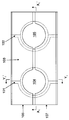
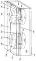
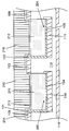
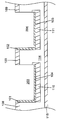
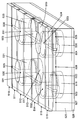
- FIGS. 2 and 3 A plan view and a bird's-eye view of the solid-state imaging device in which the CCD solid-state imaging devices according to the first embodiment of the present invention are arranged in one row and two columns are shown in FIGS. 2 and 3, respectively.
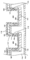
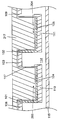
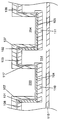
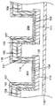
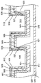
- 4 is a cross-sectional view taken along the line X 1 -X 1 ′ in FIG. 2
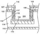
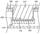
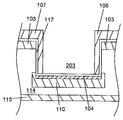
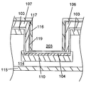
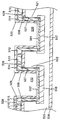
- FIG. 5 is a cross-sectional view taken along the line Y 1 -Y 1 ′ in FIG.
- a p-type well region 114 is formed on the n-type substrate 115, A silicon hole 203 is formed in the p-type well 114, A p + type region 104 is formed at the bottom of the silicon hole 203, A p + type element isolation region 101 formed so as to be connected to the p + type region 104 is formed on a part of the side wall of the silicon hole 203.
- n-type photoelectric conversion region 110 is formed in the lower part of the p + type region 104 and the other part of the side wall at the bottom of the silicon hole 203, Transfer electrodes 106 and 107 are formed on the side wall of the silicon hole 203 via the gate insulating film 117,
- the n-type CCD channel 103 is formed on the surface of the p-type well 114 and the other part of the upper side wall of the silicon hole 203,
- a readout channel 112 is formed in a region sandwiched between the n-type photoelectric conversion region 110 and the n-type CCD channel 103.
- a p-type well region 114 is formed on the n-type substrate 115, A silicon hole 204 is formed in the p-type well 114, A p + type region 105 is formed at the bottom of the silicon hole 204, A p + -type element isolation region 102 formed so as to be connected to the p + -type region 105 is formed on a part of the side wall of the silicon hole 204, An n-type photoelectric conversion region 111 is formed in the lower portion of the p + -type region 105 and the other part of the side wall at the bottom of the silicon hole 204, Transfer electrodes 106 and 107 are formed on the side wall of the silicon hole 204 via the gate insulating film 117, An n-type CCD channel region 109 is formed on the surface of the p-type well 114 and the other part of the side wall above the silicon hole 204, A readout channel 113 is formed in a region sandwiched between the n-type photoelectric conversion region 111 and the n-type
- a p + -type element isolation region 101 is formed between the n-type CCD channel regions 108 and 103 so that the channel regions do not contact each other.
- a p + type element isolation region 102 is formed between the n type CCD channel regions 103 and 109 so that the channel regions do not contact each other.
- a metal shielding film 116 is formed on the transfer electrodes 106 and 107 and on the side walls of the silicon holes 203 and 204 with an insulating film 119 interposed therebetween.
- the transfer electrode 106 or 107 When a read signal is applied to the transfer electrode 106 or 107, the signal charge accumulated in the n-type photoelectric conversion region 110 as a charge accumulation layer is read out to the n-type CCD channel region 103 through the read channel 112.
- the read signal charges are transferred in the vertical (Y 1 -Y 1 ′) direction by the transfer electrodes 106 and 107.
- FIGS. 26 and 27 a plan view and a bird's-eye view of a part of the solid-state imaging device according to the second embodiment of the present invention in which a plurality of CCD solid-state imaging devices according to the first embodiment are arranged in a matrix are shown in FIGS. 26 and 27, respectively. Shown in 28 is a cross-sectional view taken along the line X 3 -X 3 ′ in FIG. 26, and FIG. 29 is a cross-sectional view taken along the line Y 3 -Y 3 ′ in FIG. 26.
- solid-state imaging devices having p + -type regions 501 and 502 are arranged on a semiconductor substrate in a vertical (Y 3 -Y 3 ′) direction (column direction) at a predetermined interval (vertical pixel pitch VP).
- first solid-state imaging device array A solid-state image sensor having p + -type regions 503 and 504 adjacent to each other in the first solid-state image sensor array in the same vertical direction and having the same vertical interval as the first solid-state image sensor array ( They are arranged in the vertical direction at a vertical pixel pitch VP) (second solid-state imaging device array).
- the first solid-state image sensor array and the second solid-state image sensor array are arranged at the same interval (horizontal pixel pitch HP) as the vertical pixel pitch.
- the solid-state imaging devices having the p + -type regions 501, 502, 503, and 504 are arranged in a so-called matrix form.
- An n-type CCD channel region 508 for reading the generated signal charge and transferring it in the vertical direction is provided.
- n-type CCD channel regions 507 and 509 are provided to read out signal charges generated in other photodiodes and transfer them in the vertical direction.
- the n-type CCD channel region extends in the vertical direction between the silicon holes arranged in a matrix.
- p + -type element isolation regions 505 and 506 are provided so that the n-type CCD channel regions are separated from each other and do not contact each other. Further, in order to apply a voltage to the p + -type regions 501 and 502, the p + -type element isolation region 505 is also formed on part of the side walls of the silicon holes 530 and 532 and connected to the p + -type regions 501 and 502. Further, in order to apply a voltage to the p + -type regions 503 and 504, the p + -type element isolation region 506 is also formed in part of the side walls of the silicon holes 531 and 533 and connected to the p + -type regions 503 and 504.
- the p + type element isolation regions 505 and 506 are provided along the axes of the first and second solid-state imaging element rows and the outer edge of the silicon hole.
- the p + type element isolation region is provided so that adjacent n type CCD channel regions are not in contact with each other, formed on a part of the side wall of the silicon hole, and connected to the p + type region at the bottom of the silicon hole. for example, it is also possible to staggered the p + -type element isolation region 505, 506 from the arrangement of Figure 25 in the X 3 direction.
- transfer electrodes 510, 511, 515, and 516 are provided for transferring the signal charges read from the photodiodes to the n-type CCD channel regions 507, 508, and 509 in the vertical direction.
- a readout signal is applied to the transfer electrode 514, signal charges accumulated in the photodiodes 502 and 504 are read out to the n-type CCD channel regions 508 and 509 through the readout channel.
- the transfer electrode extends in the horizontal direction between the silicon holes arranged in a matrix.
- a solid-state imaging device having a p + region 501 is: A p-type well region 525 is formed on the n-type substrate 526, and A silicon hole 530 is formed in the p-type well 525, A p + type region 501 is formed at the bottom of the silicon hole 530, A p + -type element isolation region 505 formed so as to be connected to the p + -type region 501 is formed on a part of the side wall of the silicon hole 530.
- An n-type photoelectric conversion region 517 is formed in the lower part of the p + -type region 501 and the other part of the sidewall of the bottom of the silicon hole 530, Transfer electrodes 511 and 512 are formed on the side wall of the silicon hole 530 via the gate insulating film 527, An n-type CCD channel 508 is formed on the surface of the p-type well 525 and the other part of the upper side wall of the silicon hole 530, A readout channel 521 is formed in a region sandwiched between the n-type photoelectric conversion region 517 and the n-type CCD channel 508.
- the solid-state imaging device having the p + region 502 is A p-type well region 525 is formed on the n-type substrate 526, and A silicon hole 532 is formed in the p-type well 525, A p + type region 502 is formed at the bottom of the silicon hole 532, A p + type element isolation region 505 formed so as to be connected to the p + type region 502 is formed on a part of the side wall of the silicon hole 532, An n-type photoelectric conversion region 518 is formed in the lower part of the p + -type region 502 and the other part of the side wall of the bottom of the silicon hole 532, Transfer electrodes 514 and 515 are formed on the side wall of the silicon hole 532 via the gate insulating film 527, An n-type CCD channel 508 is formed on the surface of the p-type well 525 and the other part of the upper side wall of the silicon hole 532, A readout channel 522 is formed in a region sandwiched between the n-type
- the solid-state imaging device having the p + region 503 is A p-type well region 525 is formed on the n-type substrate 526, and A silicon hole 531 is formed in the p-type well 525, A p + type region 503 is formed at the bottom of the silicon hole 531, A p + type element isolation region 506 formed so as to be connected to the p + type region 503 is formed on a part of the side wall of the silicon hole 531.
- An n-type photoelectric conversion region 519 is formed in the lower part of the p + type region 503 and the other part of the side wall at the bottom of the silicon hole 531.
- Transfer electrodes 511 and 512 are formed on the side wall of the silicon hole 531 via a gate insulating film 527, An n-type CCD channel 509 is formed on the surface of the p-type well 525 and the other part of the upper side wall of the silicon hole 531, A readout channel 523 is formed in a region sandwiched between the n-type photoelectric conversion region 519 and the n-type CCD channel 509.
- the solid-state imaging device having the p + region 504 is A p-type well region 525 is formed on the n-type substrate 526, and A silicon hole 533 is formed in the p-type well 525, A p + type region 504 is formed at the bottom of the silicon hole 533, A p + -type element isolation region 506 formed so as to be connected to the p + -type region 504 is formed on a part of the side wall of the silicon hole 533, An n-type photoelectric conversion region 520 is formed in the lower part of the p + -type region 504 and the other part of the side wall of the bottom of the silicon hole 533, Transfer electrodes 514 and 515 are formed on the side wall of the silicon hole 533 through the gate insulating film 527, An n-type CCD channel 509 is formed on the surface of the p-type well 525 and another part of the side wall at the top of the silicon hole 533, A readout channel 524 is formed in a region sandwiched between
- a metal shielding film 529 is formed on the transfer electrodes 510, 511, 512, 513, 514, 515, 516, and on the side walls of the silicon holes 501, 502, 503, 504 via the insulating film 528.
- the transfer electrodes 510, 511, 512, 513 which extend in the row direction so as to pass between the silicon holes of the adjacent solid-state image pickup element rows, pass between the silicon holes of the adjacent solid-state image pickup element rows.
- 514, 515, and 516 are provided and are spaced apart by a predetermined distance. It is formed on the side surface of the silicon hole via transfer electrodes 511, 512, 514 and 515 adjacent to the silicon hole and a gate insulating film.
- the transfer electrodes 510, 511, 512, 513, 514, 515, and 516, together with the n-type CCD channel region, constitute a vertical charge transfer device (VCCD) that transfers signal charges generated by the photodiodes in the vertical direction.
- VCCD vertical charge transfer device
- the VCCD is driven in three phases ( ⁇ 1 to ⁇ 3), and the signal charges generated in the photodiode are transferred in the vertical direction by three transfer electrodes driven at different phases for each photodiode.
- the VCCD is three-phase driven, but it will be apparent to those skilled in the art that the VCCD can be configured to drive in any suitable number of phases.
- the solid-state imaging device in which the CCD solid-state imaging devices are arranged in a matrix is shown.
- the CCD solid-state imaging device is formed in a honeycomb shape. You may arrange. Therefore, as a third embodiment of the present invention, a solid-state imaging device in which the CCD solid-state imaging device of the first embodiment is arranged in a honeycomb shape will be described.
- a plan view and a bird's-eye view of a part of a solid-state imaging device in which CCD solid-state imaging devices are arranged in a honeycomb shape are shown in FIGS. 22 and 23, respectively.
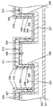
- 24 is a cross-sectional view taken along the line X 2 -X 2 ′ of FIG. 22
- FIG. 25 is a cross-sectional view taken along the line Y 2 -Y 2 ′ of FIG.
- solid-state image sensors having p + -type regions 301 and 302 are arranged on a semiconductor substrate in a vertical (Y 2 -Y 2 ') direction (column direction) at a predetermined interval (vertical pixel pitch VP).
- first solid-state imaging device array A solid-state image sensor having p + -type regions 303 and 304 at the same interval (horizontal pixel pitch HP) as the vertical pixel pitch and the first solid-state image sensor array is the same as the first solid-state image sensor array.
- a solid-state image sensor having p + -type regions 305 and 306 at a distance equal to 1/2 of the second solid-state image sensor array and the same vertical pixel pitch (horizontal pixel pitch HP) as the first solid-state image sensor array. They are arranged in the vertical direction at the same predetermined interval, and are arranged so as to be shifted by 1/2 with respect to the vertical pixel pitch VP in the vertical direction with respect to the second solid-state image sensor array (third solid-state image sensor array). That is, the solid-state imaging devices having the p + regions 301, 302, 303, 304, 305, and 306 are arranged in a so-called honeycomb shape.
- n-type CCD channel region 331 is provided for reading out the signal charges and transferring them in the vertical direction.
- An n-type CCD channel region 312 is provided for reading out and transferring in the vertical direction.
- an n-type CCD channel region 313 is provided for reading out signal charges generated by the photodiodes having the p + regions 305 and 306 and transferring them in the vertical direction.
- an n-type CCD channel region 310 is provided for reading out signal charges generated by the photodiode and transferring them in the vertical direction.
- These n-type CCD channel regions extend in the vertical direction while meandering between the silicon holes arranged in a honeycomb shape.
- p + type element isolation regions 307, 308, and 309 are provided so that the n type CCD channel regions are not separated from each other and contact with each other.
- the p + -type element isolation region 307 is also formed on part of the side walls of the silicon holes 339 and 331 and is connected to the p + -type regions 301 and 302. Further, in order to apply a voltage to the p + -type regions 303 and 304, the p + -type element isolation region 308 is also formed on a part of the side walls of the silicon holes 334 and 333 and connected to the p + -type regions 303 and 304.
- the p + -type element isolation region 309 is also formed on a part of the side walls of the silicon holes 343 and 332 and connected to the p + -type regions 305 and 306.
- the p + type element isolation regions 307, 308, and 309 are provided along the axes of the first, second, and third solid-state imaging element rows and the outer edge of the silicon hole.
- the element isolation region may be provided so that adjacent n-type CCD channel regions are not in contact with each other, formed on a part of the side wall of the silicon hole, and connected to the p + type region at the bottom of the silicon hole.
- the p + -type element isolation region 307, 308, 309 may be staggered in the X 2 direction from the arrangement of FIG. 21.
- Solid-state imaging device having silicon holes 339 and 343 in the first solid-state imaging device row in which solid-state imaging devices having p + regions 301 and 305 are arranged in the horizontal (X 2 ⁇ X 2 ′) direction (row direction) and p + region 303 Are provided between the silicon holes 334 of the second solid-state imaging device row arranged in the horizontal direction.
- the third solid-state imaging in which the solid-state imaging devices having the p + regions 302 and 306 are arranged in the horizontal direction and the silicon holes 334 in the second solid-state imaging device row in which the solid-state imaging devices having the p + region 303 are arranged in the horizontal direction.
- the solid-state imaging device having the p + region 301 is A p-type well region 320 is formed on the n-type substrate 321, A silicon hole 339 is formed in the p-type well 320, A p + type region 301 is formed at the bottom of the silicon hole 339, A p + -type element isolation region 307 formed so as to be connected to the p + -type region 301 is formed on a part of the side wall of the silicon hole 339, An n-type photoelectric conversion region 322 is formed in the lower part of the p + -type region 301 and the other part of the side wall of the bottom of the silicon hole 339, A transfer electrode 314 is formed on the side wall of the silicon hole 339 via a gate insulating film 328, An n-type CCD channel 311 is formed on the surface of the p-type well 320 and another part of the side wall above the silicon hole 339, A readout channel 340 is formed in a region sandwiched between the n-type photoelectric conversion
- the solid-state imaging device having the p + region 302 is A p-type well region 320 is formed on the n-type substrate 321, A silicon hole 331 is formed in the p-type well 320, A p + type region 302 is formed at the bottom of the silicon hole 331, A p + -type element isolation region 307 formed so as to be connected to the p + -type region 302 is formed on a part of the side wall of the silicon hole 331.
- An n-type photoelectric conversion region 323 is formed in the lower part of the p + type region 302 and the other part of the side wall of the bottom of the silicon hole 331, Transfer electrodes 317 and 318 are formed on the side wall of the silicon hole 331 through the gate insulating film 328, An n-type CCD channel 311 is formed on the surface of the p-type well 320 and the other part of the upper side wall of the silicon hole 331, A readout channel 335 is formed in a region sandwiched between the n-type photoelectric conversion region 323 and the n-type CCD channel 311.
- the solid-state imaging device having the p + region 303 is A p-type well region 320 is formed on the n-type substrate 321, A silicon hole 334 is formed in the p-type well 320, A p + type region 303 is formed at the bottom of the silicon hole 334, A p + type element isolation region 308 formed so as to be connected to the p + type region 303 is formed on a part of the side wall of the silicon hole 334, An n-type photoelectric conversion region 324 is formed in the lower part of the p + type region 303 and the other part of the side wall of the bottom of the silicon hole 334, Transfer electrodes 315 and 316 are formed on the side wall of the silicon hole 334 via a gate insulating film 328, An n-type CCD channel 312 is formed on the surface of the p-type well 320 and the other part of the side wall above the silicon hole 334, A readout channel 338 is formed in a region sandwiched between the n-type photoelectric conversion region 3
- a solid-state imaging device having a p + region 304 is: A p-type well region 320 is formed on the n-type substrate 321, A silicon hole 333 is formed in the p-type well 320, A p + type region 304 is formed at the bottom of the silicon hole 333, A p + type element isolation region 308 formed so as to be connected to the p + type region 304 is formed on a part of the side wall of the silicon hole 333, An n-type photoelectric conversion region 325 is formed in the lower part of the p + type region 304 and the other part of the side wall of the bottom of the silicon hole 333, A transfer electrode 319 is formed on the side wall of the silicon hole 333 through a gate insulating film 328, An n-type CCD channel 312 is formed on the surface of the p-type well 320 and the other part of the upper side wall of the silicon hole 333, A readout channel 337 is formed in a region sandwiched between the n-type photoelectric conversion region 3
- the solid-state imaging device having the p + region 305 is A p-type well region 320 is formed on the n-type substrate 321, A silicon hole 343 is formed in the p-type well 320, A p + type region 305 is formed at the bottom of the silicon hole 343, A p + type element isolation region 309 formed so as to be connected to the p + type region 305 is formed on a part of the side wall of the silicon hole 343.
- An n-type photoelectric conversion region 326 is formed in the lower part of the p + -type region 305 and the other part of the side wall of the bottom of the silicon hole 343,
- a transfer electrode 314 is formed on the side wall of the silicon hole 343 through a gate insulating film 328,
- An n-type CCD channel 313 is formed on the surface of the p-type well 320 and the other part of the upper side wall of the silicon hole 343.
- a readout channel 341 is formed in a region sandwiched between the n-type photoelectric conversion region 326 and the n-type CCD channel 313.
- a solid-state imaging device having a p + region 306 is: A p-type well region 320 is formed on the n-type substrate 321, A silicon hole 332 is formed in the p-type well 320, A p + type region 306 is formed at the bottom of the silicon hole 332; A p + type element isolation region 309 formed so as to be connected to the p + type region 306 is formed on a part of the side wall of the silicon hole 332, An n-type photoelectric conversion region 327 is formed in the lower part of the p + -type region 306 and the other part of the side wall at the bottom of the silicon hole 332, Transfer electrodes 317 and 318 are formed on the side wall of the silicon hole 332 via the gate insulating film 328, An n-type CCD channel 313 is formed on the surface of the p-type well 320 and another part of the side wall above the silicon hole 332, A readout channel 336 is formed in a region sandwiched between the n-type photoelectric conversion region 327
- a metal shielding film 330 is formed on the transfer electrodes 314, 315, 316, 317, 318, 319 and on the side walls of the silicon holes 339, 331, 334, 333, 343, and 332 through an insulating film 329.
- the transfer electrodes 314, 315, 316, 317 which extend in the row direction so as to pass between the silicon holes of the adjacent solid-state image sensor rows, are arranged between the silicon holes of the adjacent solid-state image sensor rows. 318 and 319 are provided.
- the transfer electrodes 314, 315, 316, 317, 318, and 319 are formed on the side surface of the silicon hole via the gate insulating film 328, and are arranged at a predetermined interval.
- the transfer electrodes 314, 315, 316, 317, 318, and 319 together with the n-type CCD channel region constitute a vertical charge transfer device (VCCD) that transfers signal charges generated by the photodiodes in the vertical direction.
- VCCD vertical charge transfer device
- the VCCD is driven in four phases ( ⁇ 1 to ⁇ 4), and signal charges generated in the photodiodes are transferred in the vertical direction by four transfer electrodes driven at different phases for each photodiode.
- the VCCD is four-phase driven, but it will be apparent to those skilled in the art that the VCCD can be configured to drive in any suitable number of phases.
- a color filter, a microlens, and the like are formed on the metal shielding film through a protective film and a flattening film, as in a normal CCD image sensor.
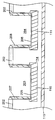
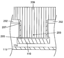
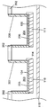
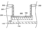
- a p-type well region 114 is formed on an n-type substrate 115, and an oxide film 201 is formed thereon (FIGS. 6A and 6B).
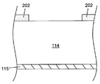
- the oxide film is etched to form an oxide film mask 202 (FIGS. 7A and 7B).
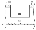
- Silicon is etched to form silicon holes 203 and 204 (FIGS. 8A and 8B).
- oxide films 205 and 206 In order to prevent ion channeling during ion implantation, oxidation is performed to form oxide films 205 and 206, and polysilicon is deposited and etched to form masks during ion implantation to form sidewalls 207 and 208. (FIGS. 9A and 9B).
- Implant phosphorus or arsenic and anneal to form n-type photoelectric conversion regions 110 and 111 FIGGS. 10A and 10B.
- resists 209 and 210 are formed, and polysilicon is etched (FIGS. 11A and 11B).
- the resist is peeled off and boron is implanted to form the p + regions 104 and 105 (FIGS. 12A and 12B).
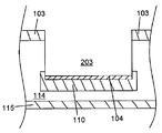
- the polysilicon and the oxide film are peeled off (FIGS. 13A and 13B).
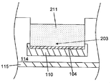
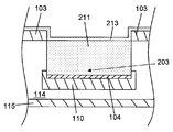
- oxide film is deposited, planarized and etched back to form oxide films 211 and 212 (FIGS. 14A and 14B).
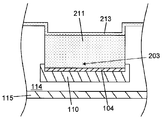
- An oxide film 213 is deposited to prevent ion channeling during ion implantation (FIGS. 15A and 15B).
- Implant phosphorus or arsenic to form n-type CCD channel regions 103, 108, and 109 (FIGS. 16A and 16B).
- Resist 214, 215, 216 for forming p + type element isolation region is formed, and boron is implanted to form p + type element isolation regions 101, 102 (FIGS. 17A and 17B).
- the resist is peeled off and the oxide film is peeled off (FIGS. 18A and 18B).
- a gate insulating film 117 is formed, polysilicon 217 is deposited, and planarized (FIGS. 19A and 19B).
- the polysilicon is etched to form transfer electrodes 106 and 107 (FIGS. 20A and 20B).
- An insulating film 119 is deposited, a metal shielding film 116 is deposited, and etching is performed (FIGS. 21A and 21B).
- the transfer electrode can be configured using an electrode material generally used in a semiconductor process or a solid-state device.
- an electrode material generally used in a semiconductor process or a solid-state device.
- low resistance polysilicon tungsten (W), molybdenum (Mo), tungsten silicide (WSi), molybdenum silicide (MoSi), titanium silicide (TiSi), tantalum silicide (TaSi), and copper silicide (CuSi).
- the transfer electrode may be formed by laminating a plurality of these electrode materials without interposing an insulating film.
- the metal shielding film is, for example, a metal film such as aluminum (Al), chromium (Cr), tungsten (W), titanium (Ti), molybdenum (Mo), or an alloy film made of two or more of these metals.
- a metal film such as aluminum (Al), chromium (Cr), tungsten (W), titanium (Ti), molybdenum (Mo), or an alloy film made of two or more of these metals.
- it can be formed of a multilayer metal film or the like that is a combination of two or more selected from the group including the metal film and the alloy film.
- FIG. 1 is a plan view of a CCD solid-state imaging device according to the present invention.
- 1 is a bird's-eye view of a CCD solid-state imaging device according to the present invention.
- FIG. 3 is a cross-sectional view taken along the line X 1 -X 1 ′ in FIG.
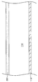
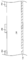
- FIG. 3 is a sectional view taken along the line Y 1 -Y 1 ′ of FIG. X 1 -X 1 ′ cross-sectional process drawing showing a manufacturing example of a CCD solid-state imaging device according to the present invention.
- FIG. 1 is a plan view of a CCD solid-state imaging device according to the present invention.
- 1 is a bird's-eye view of a CCD solid-state imaging device according to the present invention.
- FIG. 3 is a cross-sectional view taken along the line X 1 -X 1 ′ in FIG.
- FIG. 3 is a sectional view taken along the line Y 1 -Y 1 ′ of FIG.
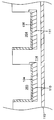
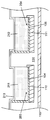
- FIG. 4 is a Y 1 -Y 1 ′ cross-sectional process drawing showing a manufacturing example of a CCD solid-state imaging device according to the present invention.
- X 1 -X 1 ′ cross-sectional process drawing showing a manufacturing example of a CCD solid-state imaging device according to the present invention.
- FIG. 4 is a Y 1 -Y 1 ′ cross-sectional process drawing showing a manufacturing example of a CCD solid-state imaging device according to the present invention.
- FIG. 23 is a cross-sectional view taken along the line X 2 -X 2 ′ in FIG.
- FIG. 23 is a sectional view taken along the line Y 2 -Y 2 ′ of FIG.
- FIG. 27 is a sectional view taken along the line X 3 -X 3 ′ in FIG. 26.
- FIG. 27 is a sectional view taken along the line Y 3 -Y 3 ′ of FIG.
Landscapes
- Solid State Image Pick-Up Elements (AREA)
- Transforming Light Signals Into Electric Signals (AREA)
Priority Applications (11)
| Application Number | Priority Date | Filing Date | Title |
|---|---|---|---|
| PCT/JP2008/069321 WO2010046994A1 (ja) | 2008-10-24 | 2008-10-24 | 固体撮像素子、固体撮像装置及びその製造方法 |
| SG200906919-6A SG161176A1 (en) | 2008-10-24 | 2009-10-16 | Solid-state image pickup element, solid-state image pickup device and production method therefor |
| TW098135560A TWI538182B (zh) | 2008-10-24 | 2009-10-21 | 固體攝像元件、固體攝像裝置以及其製造方法 |
| US12/603,001 US7956388B2 (en) | 2008-10-24 | 2009-10-21 | Solid-state image pickup element and solid-state image pickup device |
| KR1020090101455A KR101274794B1 (ko) | 2008-10-24 | 2009-10-23 | 고체촬상소자, 고체촬상장치 및 그 제조방법 |
| JP2009244179A JP5311666B2 (ja) | 2008-10-24 | 2009-10-23 | 固体撮像素子の製造方法 |
| EP09173948.2A EP2180516A3 (en) | 2008-10-24 | 2009-10-23 | Solid-state image pickup element, solid-state image pickup device and production method therefor |
| PCT/JP2009/068320 WO2010047412A1 (ja) | 2008-10-24 | 2009-10-26 | 固体撮像素子、固体撮像装置及びその製造方法 |
| CN2009101806404A CN101728410B (zh) | 2008-10-24 | 2009-10-26 | 固态摄像元件、固态摄像装置及其制造方法 |
| US12/970,272 US8114695B2 (en) | 2008-10-24 | 2010-12-16 | Solid-state image pickup element, solid-state image pickup device and production method therefor |
| US13/115,715 US8115237B2 (en) | 2008-10-24 | 2011-05-25 | Solid-state image pickup element and solid-state image pickup device having a transfer electrode formed on the entire sidewall of a hole |
Applications Claiming Priority (1)
| Application Number | Priority Date | Filing Date | Title |
|---|---|---|---|
| PCT/JP2008/069321 WO2010046994A1 (ja) | 2008-10-24 | 2008-10-24 | 固体撮像素子、固体撮像装置及びその製造方法 |
Publications (1)
| Publication Number | Publication Date |
|---|---|
| WO2010046994A1 true WO2010046994A1 (ja) | 2010-04-29 |
Family
ID=41506530
Family Applications (2)
| Application Number | Title | Priority Date | Filing Date |
|---|---|---|---|
| PCT/JP2008/069321 Ceased WO2010046994A1 (ja) | 2008-10-24 | 2008-10-24 | 固体撮像素子、固体撮像装置及びその製造方法 |
| PCT/JP2009/068320 Ceased WO2010047412A1 (ja) | 2008-10-24 | 2009-10-26 | 固体撮像素子、固体撮像装置及びその製造方法 |
Family Applications After (1)
| Application Number | Title | Priority Date | Filing Date |
|---|---|---|---|
| PCT/JP2009/068320 Ceased WO2010047412A1 (ja) | 2008-10-24 | 2009-10-26 | 固体撮像素子、固体撮像装置及びその製造方法 |
Country Status (7)
| Country | Link |
|---|---|
| EP (1) | EP2180516A3 (enExample) |
| JP (1) | JP5311666B2 (enExample) |
| KR (1) | KR101274794B1 (enExample) |
| CN (1) | CN101728410B (enExample) |
| SG (1) | SG161176A1 (enExample) |
| TW (1) | TWI538182B (enExample) |
| WO (2) | WO2010046994A1 (enExample) |
Families Citing this family (2)
| Publication number | Priority date | Publication date | Assignee | Title |
|---|---|---|---|---|
| DE202010016472U1 (de) | 2009-12-15 | 2011-03-24 | Isensee, Gerrit Ragnar Ulrich Friedrich, Maspalomas | Modul zur Simulation einer belegten Sitzkontaktmatte in Fahrzeugen |
| JP2024069731A (ja) * | 2021-03-17 | 2024-05-22 | ソニーセミコンダクタソリューションズ株式会社 | 光電変換素子及び撮像装置 |
Citations (11)
| Publication number | Priority date | Publication date | Assignee | Title |
|---|---|---|---|---|
| JPS59129463A (ja) * | 1983-01-14 | 1984-07-25 | Nec Corp | 固体撮像装置 |
| JPH01168059A (ja) * | 1987-12-24 | 1989-07-03 | Fuji Photo Film Co Ltd | 固体撮像素子 |
| JPH02278874A (ja) * | 1989-04-20 | 1990-11-15 | Hitachi Ltd | 固体撮像素子及びその製造方法 |
| JPH02304976A (ja) * | 1989-05-19 | 1990-12-18 | Nec Corp | 固体撮像素子 |
| JPH03161970A (ja) * | 1989-11-21 | 1991-07-11 | Toshiba Corp | 固体撮像装置 |
| JPH03285335A (ja) * | 1990-04-02 | 1991-12-16 | Matsushita Electron Corp | 電荷転送素子の製造方法 |
| JPH0697416A (ja) * | 1992-09-14 | 1994-04-08 | Toshiba Corp | 固体撮像装置及びその製造方法 |
| JPH06252375A (ja) * | 1993-03-01 | 1994-09-09 | Hitachi Ltd | 固体撮像装置 |
| JPH06268189A (ja) * | 1993-03-15 | 1994-09-22 | Toshiba Corp | 固体撮像装置 |
| JPH10107249A (ja) * | 1996-09-27 | 1998-04-24 | Sony Corp | 固体撮像素子の製造方法 |
| JP2001308309A (ja) * | 2000-04-26 | 2001-11-02 | Sony Corp | 固体撮像素子及びその製造方法 |
Family Cites Families (9)
| Publication number | Priority date | Publication date | Assignee | Title |
|---|---|---|---|---|
| JP2517375B2 (ja) * | 1988-12-19 | 1996-07-24 | 三菱電機株式会社 | 固体撮像装置および該装置に用いられる電荷転送装置ならびにその製造方法 |
| JPH10189936A (ja) * | 1996-12-26 | 1998-07-21 | Sony Corp | 固体撮像素子及びその製造方法 |
| KR100475733B1 (ko) * | 1997-10-07 | 2005-07-07 | 삼성전자주식회사 | 전하결합형고체촬상소자및그제조방법 |
| JP3152300B2 (ja) | 1998-09-17 | 2001-04-03 | 日本電気株式会社 | 固体撮像素子及びその製造方法 |
| JP2000196060A (ja) | 1998-12-24 | 2000-07-14 | Nec Corp | 固体撮像装置およびその製造方法 |
| EP1341235A3 (en) * | 2002-02-28 | 2006-05-10 | Canon Kabushiki Kaisha | Image pickup apparatus |
| KR100690884B1 (ko) * | 2005-04-28 | 2007-03-09 | 삼성전자주식회사 | 이미지 센서 및 그 제조 방법 |
| JP2008112831A (ja) * | 2006-10-30 | 2008-05-15 | Fujifilm Corp | 固体撮像素子及びこれを備えた撮像装置 |
| JP5114968B2 (ja) * | 2007-02-20 | 2013-01-09 | 富士通セミコンダクター株式会社 | 半導体装置及びその製造方法 |
-
2008
- 2008-10-24 WO PCT/JP2008/069321 patent/WO2010046994A1/ja not_active Ceased
-
2009
- 2009-10-16 SG SG200906919-6A patent/SG161176A1/en unknown
- 2009-10-21 TW TW098135560A patent/TWI538182B/zh active
- 2009-10-23 JP JP2009244179A patent/JP5311666B2/ja not_active Expired - Fee Related
- 2009-10-23 EP EP09173948.2A patent/EP2180516A3/en not_active Withdrawn
- 2009-10-23 KR KR1020090101455A patent/KR101274794B1/ko not_active Expired - Fee Related
- 2009-10-26 WO PCT/JP2009/068320 patent/WO2010047412A1/ja not_active Ceased
- 2009-10-26 CN CN2009101806404A patent/CN101728410B/zh active Active
Patent Citations (11)
| Publication number | Priority date | Publication date | Assignee | Title |
|---|---|---|---|---|
| JPS59129463A (ja) * | 1983-01-14 | 1984-07-25 | Nec Corp | 固体撮像装置 |
| JPH01168059A (ja) * | 1987-12-24 | 1989-07-03 | Fuji Photo Film Co Ltd | 固体撮像素子 |
| JPH02278874A (ja) * | 1989-04-20 | 1990-11-15 | Hitachi Ltd | 固体撮像素子及びその製造方法 |
| JPH02304976A (ja) * | 1989-05-19 | 1990-12-18 | Nec Corp | 固体撮像素子 |
| JPH03161970A (ja) * | 1989-11-21 | 1991-07-11 | Toshiba Corp | 固体撮像装置 |
| JPH03285335A (ja) * | 1990-04-02 | 1991-12-16 | Matsushita Electron Corp | 電荷転送素子の製造方法 |
| JPH0697416A (ja) * | 1992-09-14 | 1994-04-08 | Toshiba Corp | 固体撮像装置及びその製造方法 |
| JPH06252375A (ja) * | 1993-03-01 | 1994-09-09 | Hitachi Ltd | 固体撮像装置 |
| JPH06268189A (ja) * | 1993-03-15 | 1994-09-22 | Toshiba Corp | 固体撮像装置 |
| JPH10107249A (ja) * | 1996-09-27 | 1998-04-24 | Sony Corp | 固体撮像素子の製造方法 |
| JP2001308309A (ja) * | 2000-04-26 | 2001-11-02 | Sony Corp | 固体撮像素子及びその製造方法 |
Also Published As
| Publication number | Publication date |
|---|---|
| JP2010103540A (ja) | 2010-05-06 |
| SG161176A1 (en) | 2010-05-27 |
| CN101728410B (zh) | 2013-10-30 |
| WO2010047412A1 (ja) | 2010-04-29 |
| KR20100045944A (ko) | 2010-05-04 |
| JP5311666B2 (ja) | 2013-10-09 |
| KR101274794B1 (ko) | 2013-06-13 |
| TW201017875A (en) | 2010-05-01 |
| EP2180516A3 (en) | 2013-10-23 |
| CN101728410A (zh) | 2010-06-09 |
| EP2180516A2 (en) | 2010-04-28 |
| TWI538182B (zh) | 2016-06-11 |
Similar Documents
| Publication | Publication Date | Title |
|---|---|---|
| JP3742775B2 (ja) | 固体撮像素子 | |
| JP4429368B2 (ja) | 固体撮像素子、固体撮像装置及びその製造方法 | |
| US8114695B2 (en) | Solid-state image pickup element, solid-state image pickup device and production method therefor | |
| JP2007067379A (ja) | 固体撮像装置 | |
| JP5311666B2 (ja) | 固体撮像素子の製造方法 | |
| JP2010103540A6 (ja) | 固体撮像素子、固体撮像装置及びその製造方法 | |
| JP2005191400A (ja) | 固体撮像素子及び固体撮像素子の製造方法 | |
| JP4346364B2 (ja) | 固体撮像装置の製造方法 | |
| JP4384350B2 (ja) | 固体撮像素子 | |
| JP4797302B2 (ja) | 固体撮像素子及びその製造方法 | |
| JP2007150661A (ja) | 固体撮像装置及び固体撮像装置の駆動方法 | |
| JP3890381B2 (ja) | 固体撮像装置 | |
| JP2005044850A (ja) | 固体撮像装置 | |
| JP2007048895A (ja) | 固体撮像装置及び固体撮像装置の製造方法 | |
| JP2003243641A (ja) | 固体撮像装置 | |
| JP2009194404A (ja) | 固体撮像装置 | |
| JP2007299806A (ja) | 固体撮像装置及びその製造方法 | |
| JP2009200262A (ja) | 半導体装置およびその製造方法、固体撮像装置およびその製造方法、並びに電子情報機器 | |
| JP2006179728A (ja) | 固体撮像素子及びその製造方法 | |
| JP2009088234A (ja) | 固体撮像装置及びその製造方法 | |
| JP2007266480A (ja) | 固体撮像素子の製造方法 |
Legal Events
| Date | Code | Title | Description |
|---|---|---|---|
| 121 | Ep: the epo has been informed by wipo that ep was designated in this application |
Ref document number: 08877560 Country of ref document: EP Kind code of ref document: A1 |
|
| NENP | Non-entry into the national phase |
Ref country code: DE |
|
| 122 | Ep: pct application non-entry in european phase |
Ref document number: 08877560 Country of ref document: EP Kind code of ref document: A1 |
|
| NENP | Non-entry into the national phase |
Ref country code: JP |