WO2010029700A1 - 荷電粒子線装置 - Google Patents
荷電粒子線装置 Download PDFInfo
- Publication number
- WO2010029700A1 WO2010029700A1 PCT/JP2009/004205 JP2009004205W WO2010029700A1 WO 2010029700 A1 WO2010029700 A1 WO 2010029700A1 JP 2009004205 W JP2009004205 W JP 2009004205W WO 2010029700 A1 WO2010029700 A1 WO 2010029700A1
- Authority
- WO
- WIPO (PCT)
- Prior art keywords
- charged particle
- scanning
- particle beam
- stage
- inspection
- Prior art date
Links
Images


Classifications
-
- H—ELECTRICITY
- H01—ELECTRIC ELEMENTS
- H01J—ELECTRIC DISCHARGE TUBES OR DISCHARGE LAMPS
- H01J37/00—Discharge tubes with provision for introducing objects or material to be exposed to the discharge, e.g. for the purpose of examination or processing thereof
- H01J37/26—Electron or ion microscopes; Electron or ion diffraction tubes
- H01J37/28—Electron or ion microscopes; Electron or ion diffraction tubes with scanning beams
-
- H—ELECTRICITY
- H01—ELECTRIC ELEMENTS
- H01J—ELECTRIC DISCHARGE TUBES OR DISCHARGE LAMPS
- H01J37/00—Discharge tubes with provision for introducing objects or material to be exposed to the discharge, e.g. for the purpose of examination or processing thereof
- H01J37/02—Details
- H01J37/20—Means for supporting or positioning the objects or the material; Means for adjusting diaphragms or lenses associated with the support
-
- H—ELECTRICITY
- H01—ELECTRIC ELEMENTS
- H01J—ELECTRIC DISCHARGE TUBES OR DISCHARGE LAMPS
- H01J37/00—Discharge tubes with provision for introducing objects or material to be exposed to the discharge, e.g. for the purpose of examination or processing thereof
- H01J37/26—Electron or ion microscopes; Electron or ion diffraction tubes
- H01J37/261—Details
- H01J37/265—Controlling the tube; circuit arrangements adapted to a particular application not otherwise provided, e.g. bright-field-dark-field illumination
-
- H—ELECTRICITY
- H01—ELECTRIC ELEMENTS
- H01J—ELECTRIC DISCHARGE TUBES OR DISCHARGE LAMPS
- H01J2237/00—Discharge tubes exposing object to beam, e.g. for analysis treatment, etching, imaging
- H01J2237/20—Positioning, supporting, modifying or maintaining the physical state of objects being observed or treated
- H01J2237/202—Movement
- H01J2237/20278—Motorised movement
- H01J2237/20285—Motorised movement computer-controlled
-
- H—ELECTRICITY
- H01—ELECTRIC ELEMENTS
- H01J—ELECTRIC DISCHARGE TUBES OR DISCHARGE LAMPS
- H01J2237/00—Discharge tubes exposing object to beam, e.g. for analysis treatment, etching, imaging
- H01J2237/26—Electron or ion microscopes
- H01J2237/28—Scanning microscopes
- H01J2237/2813—Scanning microscopes characterised by the application
- H01J2237/2817—Pattern inspection
Definitions
- the present invention relates to a charged particle beam apparatus for inspecting a substrate on which a circuit pattern is formed, such as a semiconductor substrate of a semiconductor device or a deflection array substrate of a liquid crystal display, using a charged particle beam as an inspection sample.
- a defect such as a pattern disconnection or short circuit, a scratch or a foreign substance affects the performance of the semiconductor device or the liquid crystal manufactured from the substrate. Therefore, it is important to find these defects early.
- inspection devices that use electron beams to apply electron microscope technology have been put into practical use.
- Defect detection by an inspection apparatus using charged particle beams is based on the fact that the above circuit pattern is a repeated pattern having the same shape, and acquires images of a region having the repeated pattern and an adjacent region to the image. It is executed by comparing.
- a defect detection method is also used in which an image of a pattern having no defect is stored in a device as a reference image and compared with a detected image.
- pixels having a difference in signal intensity such as brightness are extracted from the acquired image in pixel units, and those whose signal intensity exceeds a predetermined threshold are determined as defect candidates, and their representative coordinates are calculated.
- the reason for selecting a defect candidate is that noise is superimposed on the image itself due to various factors, and this may be detected as a defect. Whether or not the defect is a true defect is determined by the operator visually checking the defect candidate image.
- the inspection speed of the inspection apparatus is basically limited by the image acquisition speed.
- the area that can be imaged at once with an inspection device that uses charged particle beams is very small compared to the area of the substrate that is the object to be inspected, so inspection time can be reduced or inspection speed can be improved without reducing inspection accuracy.
- Various techniques have been tried.
- a sampling method (hereinafter referred to as swath sampling) that thins out the number of scanning stripes to be acquired at the time of imaging is known.
- swath sampling a sampling method that thins out the number of scanning stripes to be acquired at the time of imaging.
- Patent Document 1 Patent Document 2, Patent Document 2, or Non-Patent Document 2
- the sampling rate when setting the inspection area, the number of scanning stripes set in the chip is automatically set according to the set value of the sampling rate.
- An inspection apparatus having a function is disclosed. Swath sampling reduces the imaging area on the substrate to be inspected compared to the normal inspection method, but if the imaging area is sampled by a statistically meaningful technique, the distribution of detected defect candidates, Alternatively, problems in manufacturing the substrate can be analyzed by detailed analysis of defect candidates.
- Patent Document 3 since S / N (signal-to-noise ratio) and image detection speed are a trade-off in swath sampling, a high-speed inspection can be performed by devising a defect determination method.
- RIA Reference Image Averaging
- Non-Patent Document 2 In swath sampling, the results of evaluation experiments disclosed in Non-Patent Document 2 show that up to 10% sampling is a statistically meaningful sampling rate. This corresponds to a 10 times increase in speed. Further, if the defect determination method described in Non-Patent Document 2 is combined with the 10% sampling, the speed can be increased by about 20 times.
- a typical user need is to inspect 70% (effective area) of a 300 mm wafer in one hour with a 35 nm pixel 200 Mbps clock.
- 70% effective area
- the time required for inspection is about 80 hours. Therefore, a speed increase of about 20 times that can be achieved by conventional swath sampling is insufficient, and a speed increase method of about 4 times to 10 times is required.
- An object of the present invention is to provide a charged particle beam apparatus or a substrate inspection apparatus using a charged particle beam that can extract defect candidates at a higher speed than conventional ones.
- the above-described problem is that a predetermined inspection stripe is set for a sample to be inspected having a plurality of regions in which a predetermined pattern is formed, an image of a part of the inspection stripe is acquired, and an image of the acquired partial region is obtained.
- This is solved by providing the inspection apparatus with a function of performing an inspection using the. More simply, it may be considered that an inspection skip area in which no image is acquired is set in the inspection stripe. For this reason, the inspection apparatus of the present invention has a function of acquiring the inspection image by sampling a plurality of inspection regions including the partial region while the stage on which the sample to be inspected is mounted is moved.
- the primary charged particle beam irradiation to the inspection stripe is realized by scanning the charged particle beam in a direction crossing the stage movement and the stage movement. Therefore, the sampling function is realized by executing beam scanning deflection control corresponding to the moving speed of the stage so that the primary charged particle beam is irradiated only to the region including the inspection region.
- the inspection area in which the operator is interested that is, the sampling of only the ROI (Region of Interest) (hereinafter referred to as “ROI inspection” in this specification) or the simple sampling is performed. Inspection can be executed at high speed.
- ROI inspection the sampling of only the ROI (Region of Interest)
- ROI inspection the simple sampling is performed. Inspection can be executed at high speed.
- a typical ROI region for example, an end portion, a corner portion of a memory mat formed in a semiconductor device, or all pattern portions excluding a non-pattern portion when the pattern density is low can be cited.
- the stage In order to speed up the inspection, in the embodiment of the present invention, it is preferable to move the stage at a speed higher than the image detection speed of the charged particle column that executes the beam scanning deflection control. In this case, since the image detection timing and the stage moving speed become asynchronous, beam returning deflection control for eliminating the positional deviation of the beam irradiation position caused by this is used together.
- the inspection apparatus of the present invention has a management console on which the above-mentioned ROI area dimension and repetition pitch setting screen is displayed, and is based on control parameters such as ROI area dimension setting values and repetition pitch setting values.
- the stage moving speed and the primary charged particle beam deflection control amount are calculated.
- An image is acquired using the calculated value, a trial inspection is performed by an image comparison process, and an inspection recipe is set by confirming whether the inspection conditions are good or bad.
- the longitudinal cross-sectional view which shows the structure of the inspection apparatus of a board
- the flowchart which shows the procedure of recipe preparation and an inspection.
- the screen figure which shows an example of the screen displayed on the screen of a console.
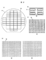
- FIG. 3 is an enlarged view of a plurality of dies shown in FIG.
- the graph which shows the time change of stage speed.
- the screen figure displayed at the time of trial inspection.
- the graph which shows the relationship between the image acquisition area
- the top view of a memory mat which shows a sampling procedure.
- FIG. 1 is a longitudinal sectional view showing the configuration of the inspection apparatus of this embodiment.
- the inspection apparatus of the present embodiment is an application of a scanning electron microscope, and the main part is housed in a vacuum vessel. This is for irradiating a substrate such as a semiconductor wafer with a primary charged particle beam.
- the inspection apparatus of this embodiment irradiates a wafer 6 placed on a sample stage 9 with a primary charged particle beam 2 generated by an electron source 1, and generates secondary charged particles 10 such as secondary electrons or reflected electrons.
- a charged particle column that is detected by the detector 13 and outputs a signal as a secondary charged particle signal, an XY stage 7 that moves the sample stage 9 in the XY plane, and a secondary charged particle signal output from the column is imaged and referenced Consists of a defect determination unit 17 that extracts a pixel having a difference in signal amount as compared with an image as a defect candidate, the above-described charged particle column, the XY stage 7, an overall control unit 18 that comprehensively controls the defect determination unit 17, and the like Is done.
- the XY stage 7 and the sample stage 9 are held in the vacuum sample chamber.
- the primary charged particle beam 2 In order to converge the energy of the primary charged particle beam 2 on the wafer 6, the primary charged particle beam 2 is narrowed down by the objective lens 4, so the diameter of the primary charged particle beam 2 is very small on the wafer 6.
- the primary charged particle beam 2 is deflected in a predetermined area on the wafer 6 by the deflector 3 and scanned on the wafer 6. By synchronizing the movement position by scanning and the detection timing of the secondary signal 10 by the detector 13, a two-dimensional image can be formed.
- a charging phenomenon may occur in which charges accumulate due to irradiation of the primary charged particle beam 2. Since the charging phenomenon changes the brightness of the image or bends the trajectory of the incident primary charged particle beam 2, the charge control electrode 5 is provided in front of the wafer 6 to control the electric field strength. I have to.
- the primary charged particle beam 2 is imaged by irradiating the standard sample piece 21, and the coordinates of the primary charged particle beam irradiation position and the focus are calibrated.
- the diameter of the primary charged particle beam 2 is very small
- the scanning width by the deflector 3 is very small compared to the size of the wafer 6, and the image formed by the primary charged particle beam 2 is very small. Therefore, when the wafer 6 is placed on the XY stage 7 before the inspection, an alignment mark for coordinate calibration provided on the wafer 6 is detected from an image with a relatively low magnification by the optical microscope 20, and the XY stage 7 is detected. Is moved so that the alignment mark is positioned below the primary charged particle beam 2 to calibrate the coordinates.
- the height of the standard specimen 21 is measured by the Z sensor 8 that measures the height of the wafer 6, and then the height of the alignment mark provided on the wafer 6 is measured.
- the excitation intensity of the objective lens 4 is adjusted so that the focal range of the primary charged particle beam 2 focused by the objective lens 4 includes the alignment mark.
- the secondary signal deflector 12 causes the secondary signal 10 to strike the reflecting plate 11 with a secondary signal deflector 12, and the second secondary signal generated on the reflecting plate 11. Electrons are detected by the detector 13.
- the overall control unit 18 controls the above-described coordinate composition operation, focus composition operation, and the like.
- a control signal a is transmitted to the deflector 3, and an excitation current intensity control signal b is transmitted to the objective lens.
- the measurement value c of the height of the wafer 6 transmitted from the Z sensor 8 is received, and a control signal d for controlling the XY stage 7 is transmitted to the XY stage 7.
- the signal detected by the detector 13 is converted into a digital signal 14 by the AD converter 15.
- the defect determination unit 17 generates an image from the digital signal 14, compares it with a reference image, extracts a plurality of pixels having a difference in brightness as defect candidates, and coordinates on the wafer 6 corresponding to the image signal
- a defect information signal e including the above is transmitted to the overall control unit 18.
- the inspection apparatus of this embodiment includes a console 17.
- the console 19 is connected to the overall control unit 18, and an image of a defect is displayed on the screen of the console 19, and the overall control unit 18 is based on the inspection condition f input on the console 19, and the deflector 3.
- Control signal a, objective lens intensity control signal b, and control signal d for controlling the XY stage 7 are calculated.
- the console 17 is provided with a keyboard and a pointing device (such as a mouse) for inputting the inspection conditions, and the apparatus user connects the keyboard and pointing device to the GUI screen displayed on the screen. Operate and input the above inspection conditions.
- FIG. 2 is a plan view of the wafer 6 to be inspected.
- the semiconductor wafer 6 is a disk-shaped silicon substrate having a diameter of 200 mm to 300 mm and a thickness of about 1 mm, and a plurality of dies 30 to be semiconductor chips are formed. Since the size of the wafer 6 is determined, the number of dies 30 formed on one wafer 6 is determined by the size of the die 30.
- one die 30 includes a plurality of memory mat groups 31 and other memory mat peripheral circuit groups. In the case of a general memory device, the pattern layout of the die 30 is composed of four memory mat groups 31. As shown in FIG. 2C, one memory mat group 31 includes a plurality of memory mats 32.
- the memory mat group 31 includes about 100 ⁇ 100 memory mats 32.
- the memory mat 32 includes a plurality of memory cells 33 having repeatability in a two-dimensional direction. Several million memory cells 33 constitute one memory mat 32.
- the memory cell 33 may be a hole (contact hole or via hole) formed in the insulating film, or may be filled with a wiring material (called a plug). Whether the wafer in this state is to be inspected depends on which manufacturing process of the semiconductor device is inspected.
- FIGS. 3A and 3B respectively show a flowchart showing recipe creation and a flowchart showing the procedure of the main inspection executed along the set recipe.
- the overall control unit 18 reads a standard recipe created and stored in advance.
- the wafer 6 to be inspected is loaded into the inspection apparatus (step 301).
- the overall control unit 18 starts the standard recipe reading process and the loading of the wafer 6 in response to an instruction input by the operator via the console 19.
- the loaded wafer 6 is mounted on the sample stage 9.
- the overall control unit 18 applies the voltage applied to the electron source 1, the excitation intensity of the objective lens 4, the voltage applied to the charging control electrode 5, and the deflector 3 based on the read standard recipe.
- Optical system conditions such as current are set, and based on the image of the standard sample piece 21, an alignment condition for obtaining a correction between the coordinates based on the alignment mark of the wafer 6 and the coordinates of the XY stage 7 of the inspection apparatus is set.
- inspection area information indicating an area to be inspected in the wafer 6 is set, and a calibration condition for registering the coordinates for acquiring an image for adjusting the light amount of the image and the initial gain of the detector 13 is set ( Step 302).
- 2D is a boundary between a region where a large number of repetitive memory cells 33 are present and a region where the memory cells 33 are not present, and defects are likely to occur in the manufacturing process. Further, since the material is different between the region where the repetitive memory cell 33 is present and the region where the memory cell 33 is not present, the corner portion image and corner portion of the memory mat 32 obtained without changing the electron optical system conditions are obtained. When the defect inspection is performed by comparing the images of the non-regions, the brightness of the pixels is different in the corners and the regions other than the corners, so that memory cells that are not actually defective are extracted as defects.
- the pattern layout of the wafer 6 is displayed on the screen of the console 19, and the corner area of the memory mat 32 is surrounded by a square on the GUI screen.
- the corner is designated by the method (step 303).
- optical system conditions for imaging this corner are set (step 304).
- the setting of which area in the die to place the inspection stripe is executed.
- the inspection stripe is set so as to include a desired memory mat corner, and thereafter, the corner setting in step 303 is executed.
- inspection conditions are set (step 305), and a trial inspection described later is executed (step 306).
- the operator determines the result of the trial inspection from the image displayed on the screen of the console 19 to confirm the suitability of the inspection conditions (step 307).
- the inspection is performed at step 305. Correct the condition. If it is determined that correction is not necessary, the recipe is stored, the wafer 6 is unloaded, and the recipe creation is terminated (step 309).
- FIG. 3B shows an inspection procedure
- the recipe stored in FIG. 3A is read (step 310), and the wafer 6 to be inspected is loaded into the inspection apparatus (step 311).
- the operator selects or designates the actual stripe to be inspected, the pixel size, the number of line additions, etc. from the inspection stripes including the memory mat corners using the console 19, and the optical system conditions Is set in the overall control unit 18 (step 312), alignment is performed for coordinate alignment between the semiconductor wafer 6 and the XY stage 7 (step 313), and calibration is performed to adjust the light quantity of the image (step 314).
- step 315 defect inspection is started, an image of the designated inspection area is acquired, a process of performing defect determination by extracting a difference by image comparison to be a defect candidate (step 315), a difference image, a comparison image, and a defect A series of processes of storing candidate representative coordinates in a storage device (not shown) (step 316) is repeated until the inspection of the predetermined die is completed.
- the wafer 6 is unloaded (step 317).
- FIG. 4 is a screen diagram showing an example of the inspection area setting screen 40 displayed on the screen of the console 19 when executing steps 303 and 304 in the flowchart of FIG.
- the map display area 41 on the left side of the screen 40 a schematic diagram showing an overall view of the die 30 shown in FIG.
- the image display area 42 on the right side of the screen 40 an image of the memory mat 32 shown in FIG.
- the image displayed in the image display area 42 is an image having coordinates designated in the map display area 41.
- the screen 40 displays an ROI condition setting unit 43 for confirming or changing the ROI condition.
- the inspection apparatus of this embodiment has a function that can set only the corner portion as the inspection region.
- a rectangular area 44 is designated on the image display area 42 in FIG. 4, and the corners of the memory mat 32 are set as inspection target areas.
- the same adjacent patterns are compared and the difference is extracted, but in the inspection of the memory mat part, since the same adjacent pattern does not exist, an image having no defect called a golden image is obtained.
- a comparison test is performed in which the golden image is compared with the acquired image and a difference is extracted.
- the inspection area setting screen 40 of FIG. 4 shows an example in which “mat angle” as the ROI, “four corners” as details, “10 ⁇ m” as dimensions, and “golden” as detection are set in the ROI condition setting unit 43. .
- an “image acquisition” button an image of the entire inspection stripe or a partial region including at least the ROI region is acquired.
- the arithmetic unit provided in the console 19 cuts out a partial image of the ROI area from the acquired images, aligns and averages them, and a golden image is created.
- the operator confirms the golden image in the image display area 42 and presses the “Done” button, whereby the golden image is stored in the recipe.
- the golden image may be generated by the defect determination unit 17.
- FIG. 5A is an enlarged view of a plurality of dies 30 shown in FIG. 2A
- FIG. 5B is an enlarged view of a part of an inspection stripe set in a certain die. is there.
- 51A, B, and C indicate a plurality of dies arranged adjacent to each other
- 52 indicates an ROI scanning region in which the inspection stripe 53 is set.
- the ROI scanning region 52 is set in the inspection stripe 53 so that the width is L and the pitch with the adjacent ROI scanning region is P.
- An arrow passing through the center of the inspection stripe 53 indicates the scanning center of the primary charged particle beam in the y direction and means the moving direction of the sample stage 7.
- the inspection apparatus moves the XY stage 7 in the direction of the arrow in the drawing along the plurality of dies 51A, B, C,. Scanning is performed in a direction orthogonal to the stage moving direction, and an image of a region including a corner set in the ROI scanning region 52 is acquired.
- the inspection stripe 53 is set so that six memory mat ends are included in one ROI scanning region 52, and therefore one ROI scanning is performed.
- the area 52 is set so as to include two sets of four corners formed by the end portions of the memory mat facing each other.
- the ROI detection area 54 corresponding to the rectangular area 44 in FIG. 4 is set at eight corner memory mat corners in the ROI scanning area 52.
- the ROI scanning area 52 and the ROI detection area 54 develop the inspection stripe arrangement information on the inspection die and the ROI information set on the inspection area setting screen of FIG. 4 on all inspection dies on the wafer 6. Is set by This calculation process is executed by the overall control unit 18.
- the width and length of the memory mat 32 are substantially constant for all the memory mats formed in the wafer, and the layout is designated in advance. Therefore, the overall control unit 18 determines the width L and pitch of the ROI scanning area 52. From the information of P, coordinate information of each ROI scanning region 52 arranged in the inspection stripe 53 can be acquired, and the timing of starting and ending the primary charged particle beam irradiation to each ROI scanning region 52 can be controlled.
- the acquired image data of each ROI scanning area 52 is transferred to the defect determination unit 17.
- the defect determination unit 17 extracts an image of the ROI detection region 54 using the layout information of the memory mat and the information of each ROI scanning region 52 calculated by the overall control unit 18, and performs a comparison operation with a golden image, which will be described later, for inspection. Execute.
- a golden image serving as a reference image for comparison inspection is created by averaging a plurality of ROI detection areas 54.
- the defect determination unit 17 compares the golden image and the plurality of ROI detection regions 54, and extracts a defect candidate image if there is a difference in brightness for each pixel.
- the defect candidate image and the defect candidate coordinates are stored in the defect determination unit 17 as defect information and can be displayed on the screen of the console 19.
- stage movement control in the ROI inspection of this embodiment will be described.
- a normal comparative inspection an image of the inspection stripe 53 shown in FIG. 5A is acquired, so that the XY stage 7 is continuously moved in the direction indicated by the arrow while being substantially perpendicular to the direction indicated by the arrow.
- the primary charged particle beam 2 is one-dimensionally scanned with the width of the inspection stripe 53.
- the inspection apparatus of the present embodiment only needs to scan only a part of the inspection stripe 53, that is, only the ROI scanning area 52 including the ROI detection area 54, so that XY compared to the normal comparison inspection.
- the moving speed of the stage 7 can be increased.
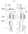
- FIGS. (C) and (f) are schematic diagrams respectively showing the positional relationship of the scanning lines in the field region of size M. 6A, 6B, and 6C are set to Vs that is faster than the stage moving speed V0 when FIGS. 6D, 6E, and 6F are set at the same stage moving speed V0 as in the conventional case. Correspond to each case. As shown in FIG.
- each ROI scanning region 52 is equal L
- the width of the inspection stripe 53 is l
- the center of the inspection stripe It is assumed that the dotted line in FIG. 6B is the scanning deflection center of the primary charged particle beam.
- the normal stage moving speed V0 means a speed at which the sample stage can move by one pixel size in a time corresponding to the image detection time for one line. In the present embodiment, this V0 may be expressed as a stage moving speed synchronized with the beam scanning.
- Image acquisition is started when the scanning line 61c enters the visual field area of length M (at the left end of the visual field area M), and while the nth scanning line 61d exists in the visual field area M, If the detection of the last pixel of the nth scanning line 61d is completed, the image can be acquired without missing the ROI scanning region 52.
- the size M of the visual field region is normally set to the maximum within the range of the maximum visual field value determined by the performance of the electron optical system.
- the electron optical system has a fixed visual field, and within the visual field, it is possible to detect an image having substantially the same effect such as aberration and distortion.
- the maximum value of the field of view is determined by the performance of the electron optical system, such as the deflection distance of the scanning deflector and the degree of field curvature, and the larger the field of view to be set, the larger the area of the sample that can be imaged at one time. High-speed inspection is possible.
- the stage moving speed Vs and the beam scanning deflection frequency are asynchronous, if nothing is done, the beam irradiation position on the ROI scanning region 52 is shifted from the position of the scanning line to be irradiated in the stage moving direction. However, it will gradually shift. Therefore, in the inspection apparatus of the present embodiment, the deviation of synchronization between the scanning deflection frequency of the beam and the stage moving speed is eliminated by returning the irradiation position of the primary charged particle beam in the same direction as the stage moving direction by the back deflection. ing.
- This control is realized by the overall control unit 18 controlling the scanning deflector 3 so as to perform the swing back deflection that eliminates the above-described synchronization shift.
- the deflection distance of the back deflection of the primary charged particle beam 2 (the beam deflection angle of the scanning deflector 3). Will grow. Therefore, a scanning deflector having a larger beam deflection angle is more advantageous in increasing the speed of stage movement.
- the stage moving speed Vs cannot be increased without limitation, and is limited by a ratio between the size M of the visual field region and the length L of the ROI scanning region 52 (essentially, the area of the ROI scanning region). Equation 1 below shows this constraint condition.
- the stage moving speed is expressed by the equation in order to capture the entire imaging region without omission. This indicates that it cannot be increased beyond the right side of 1.
- Equations 1 and 2 indicate that the maximum value of the scanning skip region is ML, that is, a condition that one ROI scanning region can be set within the field of view of size M (the leading scanning line and trailing scanning line of the ROI scanning region are The condition that can exist in the same visual field region M) is the upper limit of the scanning skip region, and if the set number or area of the ROI scanning region in the visual field region M is increased, the stage moving speed must be reduced accordingly. Is shown.
- high-speed image detection can be realized by moving the scanning position of the beam 2 within the visual field region in accordance with the region where the image is desired to be detected under the constraints of Equations 1 and 2.
- the ROI detection area 54 can be acquired even if the stage is moved at a speed as high as 6 times.
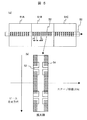
- FIG. 7 is a diagram showing a screen during execution of trial inspection displayed at the time of trial inspection in step 306.
- the trial inspection execution screen includes a map unit 70 in which the inspection stripe 53 is divided and displayed, an image display unit 71 in which a defect image is displayed, and various attribute information (RDC information) indicating defect detection conditions and defect characteristics.
- the defect information display unit 72 is displayed.
- four ROI scanning areas 52 indicated by 75 are displayed on the map unit 70.
- a rectangle 76 indicating the ROI detection area 54 and a pointer 73 for emphasizing and displaying defect candidates are displayed.
- the rectangle 76 indicating the ROI detection area 54 can be edited by switching the condition setting tab to the ROI area setting tab 77.
- the pointer 73 When the pointer 73 is clicked, an image and information of defect candidates corresponding to the pointer 73 are displayed on the image display unit 71. By moving the slide of the display threshold setting toolbar 74, the defect candidate pointer 73 displayed on the map unit 70 can be selected. In other words, the defect candidate is calculated as information on the number of thresholds or less that can be a defect candidate, and the tool bar is slid. Only candidates are displayed.
- the map unit 70 has a mode for selecting an image display mode of the image display unit 71. According to the mode, the defect candidate image, a part of the acquired image stored in the memory, and the stage are moved. The re-acquired image can be switched and displayed.
- the defect candidate image can confirm the details of the defect determination, and in a part of the acquired image, it can be confirmed whether there is another defect to be detected around the defect, and it is detected in the reacquired image It can be confirmed whether or not the defect is a true defect when observed under an optical condition of high magnification or high S / N.
- the selection mode the acquired image itself including the defect candidate can be displayed on the image display unit 71. All the controls of the GUI screen described above are executed by the arithmetic device in the console 19.
- golden image reacquisition button By clicking the golden image reacquisition button, it is possible to reacquire the golden image based on the currently acquired image and update the image.
- a reference image with fewer noise components such as defects can be created by updating the image or selecting an image to be used for addition averaging when generating a golden image.
- FIG. 8 is an explanatory diagram of the defect determination method.
- important defects (DOI) among the defects detected by the inspection apparatus include, for example, a black pattern white defect mode in which a hole portion of a contact hole that normally appears black appears white due to non-conduction, and a hole diameter of the contact hole. Due to the reduction, there are modes such as a small hole defect mode in which the black pattern appears to be small, a white defect mode in which the plug portion that normally appears white is short-circuited with the adjacent plug, and the white pattern appears to be whiter, etc. The way it looks is decided.
- the nuisance which is noise that should not be detected, includes a white bright spot defect mode in which a white bright spot is generated in the insulating film region by charging.
- the defect determination unit 17 compares the ROI detection region image 81 and the golden image 80, and first difference in ROI detection region size including pixels having different brightness (the position coordinates correspond to defect candidate positions). An image 82 is created, and a second difference image 83 having a size that includes only the vicinity of the defect candidate position is created using the difference image 82.
- the defect determination unit 17 uses the various image 84A, 84B, 84C, 84D of various defect modes such as the black pattern white defect mode, the small hole defect mode, and the white bright spot defect mode of the insulating film, which are acquired in advance.
- a matching degree determination reference image 85 corresponding to the second difference image 83 for the defect mode is created.
- the degree of coincidence is calculated for various defect modes by collating the plurality of coincidence degree determination reference images 85 with the second difference image 83.
- the table 86 shows the calculation result of the coincidence corresponding to the defect modes A to D, and it is indicated that the defect mode A has the highest coincidence.
- the defect mode of the detected defect can be known by selecting the mode with the highest degree of coincidence. Images acquired in advance may be of the same type (eg, non-passing) with different resistance values, or different defect modes (eg, non-passing defect modes with different hole resistance values and small hole defect modes with different hole diameters), or Either of both can be selected. Therefore, the inspection apparatus according to the present embodiment includes a memory for storing the image data of the defect mode in the defect determination unit 17. According to the present embodiment, not only the occurrence frequency or distribution information that does not specify the defect mode, but also a defect mode sample obtained in advance can be compared. There is a feature that information of only the mode can be obtained.
- FIG. 9 is a sequence diagram for acquiring an image used for the comparative inspection
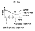
- FIG. 10 is a graph showing a change over time of the obtained signal amount.
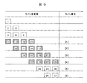
- the line number is taken in the vertical direction (when one image is acquired by a plurality of electron beam scans, the finally acquired lines are numbered in the coordinate order), and the line scan order is the image. Numbers are shown in the squares shown.
- the line [1] is obtained by performing data acquisition four times in the line scanning order No. 4, No. 7, No. 10, and No. 13, and averaging these with weighting. The weighted content will be described.
- the amount of signal obtained from the wafer 6 decreases with time.
- the surface state of the wafer can be identified, and then depends on the difference in the structure of the region irradiated with the primary charged particle beam 2.
- the amount of decrease in the signal amount differs between the normal part and the defective part depending on the difference in the charged state. For this reason, the normal part and the defective part can be identified. Therefore, by increasing the weight of the time to obtain the internal information and making the weight of the time to obtain only the surface information negative, the weight is increased compared to the case of processing using the data added without weight. The more accurate information is obtained by adding.
- the accuracy of inspection is improved by using such a transient characteristic.
- the primary charged particle beam is irradiated to the entire region in the ROI scanning region 52, and the region corresponding to the ROI detection region 54 is extracted from the acquired image and the inspection is performed. It is also possible for the inspection apparatus to adopt a configuration in which only the ROI detection region 54 is irradiated with the beam when the region 52 is scanned.
- FIG. 11 is a graph showing the relationship between the image acquisition region and the deflection voltage applied to the deflector 3 by the inspection apparatus having the function of irradiating the beam only to the ROI detection region 54.
- 11B shows a time waveform of the deflection voltage applied to the scanning deflector 3 when the entire region in the ROI scanning region 52 is imaged.
- the vertical axis represents time, and the horizontal axis represents the deflection voltage. Since the deflection voltage is zero V at the scanning deflection center, the deflection voltage is negative when scanning the upper half of the ROI scanning region 52 shown in FIG. 11A, and the deflection voltage is scanning when scanning the lower half of the ROI scanning region 52. Is positive.
- the deflection voltage value applied to the scanning deflector 3 at the time 0 is the scanning start position of the area 110a (the upper end of the area 110a). Is set to a voltage value corresponding to. That is, scanning is started in a state where the time region (i) shown in FIG.
- the deflection voltage increases as time passes and reaches a voltage value corresponding to the scanning end position of the region 110a (lower end portion of the region 110a), this time, the scanning start position of the region 110b (upper end portion of the region 110b). Is changed stepwise to a voltage value corresponding to. This step-like change corresponds to skipping the time region (ii) shown in FIG.
- the deflection voltage increases with time, and the scanning of one line is completed when the deflection value reaches a voltage value corresponding to the scanning end position (lower end of the region 110b) of the region 110b.
- the deflection voltage is reset to the voltage value at the position corresponding to the scanning start point of the next scanning line by the back deflection control in the stage moving direction.
- the scanning time (beam irradiation time) per scanning line is shortened by time (i) + (ii) + (iii) as shown in FIG. That is, the stage moving speed Vs (essentially V0) can be increased by the shortened time.
- the overall control unit 18 calculates the time waveform of the deflection voltage based on the size and arrangement pitch of the memory mat 32, the arrangement information of the ROI detection area 54 on the memory mat, and the calculated deflection. This is realized by controlling the scanning deflector 3 based on the voltage.
- the beam scanning control method for irradiating only the regions 110a and 110b including the two ROI detection regions 54 is described as an example. However, the control for performing the beam irradiation only on the ROI detection region 54, that is, the region 110a. Needless to say, the beam scanning control can be executed so as not to irradiate the region other than the ROI detection region 54 of 110b.
- the inspection apparatus realizes an inspection apparatus whose inspection speed is significantly higher than that of the prior art.
- Example 2 In the first embodiment, the example in which the ROI detection region 54 is set in the memory mat has been described.
- the defect in which the apparatus user is interested is a structural unit of a wafer having a size larger than the field of view of the detection optical system, for example, a die or a wafer In some cases, the structure unit is unevenly distributed. Therefore, in the present embodiment, an inspection method in the case where the ROI is set in a structural unit larger than that in the first embodiment will be described. Since the entire configuration of the inspection apparatus is substantially the same as that shown in FIG. 1, the description will not be repeated.
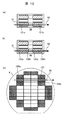
- FIGS. 12A, 12B, and 12C show examples of arrangement of the ROI of this embodiment on the die or wafer.
- FIG. 12A is a diagram showing a layout of a part of the die to be inspected, and shows an example in which the inspection stripe 53 is arranged on the memory mat group 31.
- the ROI that is an interesting examination area is the memory mat group 121a, 121b is only the memory mat group 31.
- peripheral circuit portions other than the memory mat group are out of interest because the patterns are sparse and the probability of occurrence of defects is low.
- FIG. 12B shows an example in which the ROI is set in the mammo mat outer peripheral areas 122a to 122d.
- FIG. 12C shows an example in which the ROI is set on the die on the outer periphery of the wafer.
- the wafer peripheral die 123 hatched in FIG. 12 (c) has a higher probability of occurrence of defects because the manufacturing process conditions are different compared to the inside of the wafer. Therefore, the wafer peripheral regions 124a and 124b are really interesting regions. It is.
- the region of the inspection image is set on the inspection region setting screen as shown in FIG. 4, and the overall control unit 18 executes stage movement control according to the position information of the setting region. . That is, the stage moving speed V is variable, and only the memory mat areas 121a and 121b, the mammo mat outer peripheral areas 122a to 122d and the wafer outer peripheral areas 124a and 124b are moved at a low speed, and the other areas are moved at a high speed. That is, in a region other than the predetermined region on the same inspection stripe, control is performed to move the sample stage faster than the image detection speed. Thereby, inspection time can be shortened compared with the past. (Example 3) In the present embodiment, another modified example of setting the ROI detection area will be described. The overall configuration of the inspection apparatus used in this embodiment is the same as that in FIG.
- FIG. 13A is a schematic diagram showing the arrangement of the ROI detection area in the memory mat 32 when the ROI detection area is set larger than the corner portion of the memory mat.
- the length of the ROI detection region in the vertical direction (the length in the beam scanning direction) is the same as the vertical dimension of the memory mat, and about several in the memory mat longitudinal direction (stage moving direction).
- a plurality of (three in this embodiment) partial areas 131 are set in the longitudinal direction of the memory mat.
- the area of the partial region set on the memory mat 32 is about 40% with respect to the area of the memory mat.
- the visual field region M is set to a size that includes at least one memory mat 32, and the overall control unit 18 determines the length of the partial region 131 in the stage movement direction and between the partial regions 131. Stage control corresponding to the length of the skip area is executed.
- the area setting of the partial area 131 is performed on the inspection area setting screen shown in FIG.
- the same pattern is repeated in the method using the golden image described in the first embodiment, the beam scanning direction, or the stage moving direction.
- a method using the RIA method (described in Patent Document 3 and Non-Patent Document 1), which averages repeated patterns and arranges the averaged images as a reference image, and die comparison using the same pattern for each die. Use.
- the golden image used for the comparison operation for defect detection is generated by the console 17 calculating the addition average value of the plurality of partial areas 131.
- the partial areas 131 are not necessarily set at equal intervals.
- the deviation between the scanning line position arranged in each partial region 131 and the beam irradiation position is eliminated by either adjusting the stage moving speed or controlling the returning amount of the returning deflection. Since there is a problem of machine accuracy, the controllability is higher when the adjustment is performed by the swing back deflection.
- FIG. 13B is a diagram showing the arrangement of ROI detection areas when a ROI detection area is set in units of one memory mat for a plurality of memory mats constituting a memory mat group.
- the memory mats at the four corners of the memory mat group 31, the memory mat at the middle point of the memory mat group, and the memory mat at the center of the memory mat group are set as the ROI detection area.
- only the corners of the memory cells constituting the selected memory mat are inspected. Thereby, it is possible to increase the speed according to the selection ratio of the memory mat as compared with the first embodiment.
- both the speed-up by the image sampling detection in the memory mat unit and the speed-up by the image sampling detection by the corner detection in the memory mat contribute, so the inspection time is reduced. Significantly shortened.
- the control parameter for performing the beam scanning control and the stage movement control in the memory mat 32, and the visual field area M are about the memory mat group 31.
- two types of control parameters are required for performing beam scanning control and stage movement control. That is, the corner arrangement information (the size information and position information of the rectangular area 44 shown in FIG. 4), the size information of the memory mat, and the memory necessary for acquiring the image of only the corner in the memory mat. Arrangement information (information on the size and position of the selected memory mat in the memory mat group 31) and dimensions of the memory mat group necessary for sampling in the mat group 31 in units of the memory mat 32 Information is required.
- the above control parameters may be set via the GUI by appropriately switching the visual field size of the image displayed in the image display area 42 of the examination area setting screen shown in FIG. The set control information is transferred to the overall control unit 18 and used for beam scanning control and stage movement control.
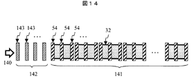
- FIG. 14 shows an arrangement relationship when three ROI detection areas are set for one memory mat. That is, in order to inspect a partial area of the memory mat 32, a plurality of ROI detection areas 54 for detecting an image and determining a defect by irradiating charged particle beams in the order in which the stage moving direction 140 is arranged are sequentially scanned.
- the ROI detection areas are completely regularly arranged in the continuous inspection area 141.
- the dummy inspection areas 143 are arranged at the same density as the continuous inspection areas 141. Note that the density of the same level is a hypothetical assumption of repeated memory mats or repeated dies, and is arranged with the same logic as that for arranging the ROI detection area 54, or determined by the stage speed. Arrange at intervals.
- the dummy inspection area can capture an image or only irradiate a charged particle beam.
- the same effect can be expected by increasing the interval of the charged particle beam scanning of one unit instead of arranging them at regular intervals.
- the same effect can also be expected by scanning with a larger beam scanning interval instead of completely scanning even between the ROI detection regions 54.
- the method of performing defect detection by comparing the previously acquired golden image 45 with the detected image has been described, but actual pattern comparison such as cell comparison, RIA method, die comparison, mat comparison, and the like. Any defect detection method such as a comparison method with a design pattern generated from design information can also be used.
- the image detection time can be about 6 times faster than the time required for obtaining an image on the entire surface of the normal wafer, and the defect frequency distribution in the ROI region can be inspected at a high throughput.
- the system There is a feature that can provide the system. Further, it is possible to provide an inspection apparatus and an inspection method for efficiently monitoring the defect occurrence frequency or the characteristic likelihood.
- SYMBOLS 2 Primary charged particle beam, 3 ... Deflector, 4 ... Objective lens, 5 ... Charge control electrode, 6 ... Wafer, 7 ... XY stage, 8 ... Z sensor, 9 ... Sample stand, 10 ... Secondary signal, 17 ... Defect determination unit, 18 ... Overall control unit, 19 ... Console, 20 ... Optical microscope, 21 ... Standard specimen, 30 ... Die, 31 ... Memory mat group, 32 ... Memory mat, 33 ... Memory cell, 41 ... Map display area , 42 ... Image display area, 43 ... ROI condition setting section, 44 ... Rectangular area, 52 ... ROI scanning area, 53 ... Inspection stripe, 54 ... ROI detection area, 70 ... Map, 71 ... Image display section, 72 ... Defect information Display unit 73... Mark, 74... Display threshold setting toolbar, 80... ROI detection area image, 81.
Abstract
Description
(実施例1)
図1は、本実施例の検査装置の構成を示す縦断面図である。本実施例の検査装置は、走査型電子顕微鏡を応用したものであり、主要部は真空容器内に収納されている。これは、半導体ウェーハなどの基板に一次荷電粒子線を照射するためである。本実施例の検査装置は、電子源1で発生した一次荷電粒子線2を試料台9に載置されたウェーハ6に照射し、発生する二次電子または反射電子などの二次荷電粒子10を検出器13で検出して二次荷電粒子信号として信号出力する荷電粒子カラム、上記試料台9をXY面内に移動させるXYステージ7、カラムから出力された二次荷電粒子信号を画像化し、参照画像と比較して信号量に差がある画素を欠陥候補として抽出する欠陥判定部17、上述の荷電粒子カラム、XYステージ7、欠陥判定部17を統括的に制御する全体制御部18などにより構成される。XYステージ7や試料台9は、真空試料室内に保持される。
欠陥判定部17は、ディジタル信号14から画像を生成し、参照画像と比較し、明るさの値に差のある複数の画素を欠陥候補として抽出し、その画像信号と対応するウェーハ6上の座標とを含む欠陥情報信号eを、全体制御部18へ送信する。
一方、ステージ移動速度の上限は、ROI走査領域52の長さLと、ROI走査領域52のステージ移動方向の配列ピッチPによっても制約を受ける。以下の数式2は、この制約条件を示す。
数式1、2は、画像を取得するROI走査領域の間に走査のスキップ領域が設定されたと考えると理解しやすい。スキップ領域の長さが大きければステージの移動速度をスピードアップできる。逆にROI走査領域の幅が大きければステージの移動速度を落とす必要がある。このため、走査領域の幅とスキップ領域の幅との比に対応してステージの移動速度が設定される。図6(b)(e)に示すように、ROI走査領域52の長さがL、ステージ移動方向への配列ピッチがPであれば、走査スキップ領域の大きさはP-Lとなる。走査スキップ間隔をSと表記するとS=P-Lであるから、P=S+Lと書き直して数式2に代入すると、
Vs≦((L+S)/L)V0 ・・・ 〔数式3〕
となり、見かけ上、数式1と等しくなる。すなわち、数式1、2は、走査スキップ領域の最大値がM-L、すなわち、サイズMの視野内にROI走査領域を1つ設定できる条件(ROI走査領域の先端走査ラインと後端走査ラインが同一の視野領域M内に存在できる条件)が走査スキップ領域の上限であり、視野領域M内へのROI走査領域の設定数あるいは面積を増やせば、その分ステージ移動速度も遅くしなければならないことを示している。
Vs-V0=ΔV=(S/L)V0 ・・・ 〔数式4〕
と変形でき、これは、ROI検査におけるステージ移動速度のV0からの増加分が、スキップ領域の長さとROI走査領域52の長さの比または視野サイズMとROI走査領域52の長さの比に応じて定まることを示している。
(実施例2)
実施例1では、ROI検出領域54をメモリマット内に設定した例について説明したが、装置ユーザの興味がある欠陥が、検出光学系の視野より大きな寸法のウェーハの構造単位、例えば、ダイやウェーハといったmmのオーダの寸法を持つ構造単位で偏在する場合がある。そこで、本実施例では、実施例1よりも大きな構造単位でROIを設定する場合の検査方法について説明する。なお、検査装置の全体構成は図1に示すものとほぼ同じであるので説明は繰り返さない。
(実施例3)
本実施例では、ROI検出領域設定の別の変形例について説明する。なお、本実施例で使用される検査装置の全体構成は、実施例2と同様、図1と同じであるものとする。
(実施例4)
本実施例では、ROI検出領域設定の更に別の変形例について説明する。図14には、1個のメモリマットに対して3個のROI検出領域を設定した場合の配置関係を示す。 即ち、メモリマット32の部分領域を検査するために、ステージ移動方向140の並び順に荷電粒子線を照射して画像を検出・欠陥判定するROI検出領域54を複数設定し、順次走査する。
Claims (10)
- 所定パターンが形成された領域を複数備える被検査試料に対し、荷電粒子線を当該被検査試料が載置されたステージの移動方向と交差する方向に走査し、当該走査により前記被検査試料から発生する二次電子または反射電子を検出して得られる信号をもとに検査画像を取得し、当該検査画像を用いて前記被検査試料を検査する荷電粒子線装置において、
前記走査の方向を制御する走査偏向器を備えた荷電粒子カラムと、
前記ステージの移動速度を制御するステージ制御手段とを備え、
前記ステージの移動中に前記領域の端部を含む複数の検査領域をサンプリングして前記検査画像を取得することを特徴とする荷電粒子線装置。 - 所定パターンが形成された領域を複数備える被検査試料に対し、荷電粒子線を当該被検査試料が載置されたステージの移動方向と交差する方向に走査し、当該走査により前記被検査試料から発生する二次電子または反射電子を検出して得られる信号をもとに検査画像を取得し、当該検査画像を用いて前記被検査試料を検査する荷電粒子線装置において、
前記ステージの移動速度を制御するステージ制御手段を備え、
前記走査が複数回実行される走査領域と、前記走査が実行されない走査スキップ領域とが前記領域に設定され、
前記ステージ制御手段は、前記ステージの移動方向での前記走査領域の幅と,前記走査スキップ領域の幅との比に対応して、前記ステージの移動速度を設定することを特徴とする荷電粒子線装置。 - 所定パターンが形成された領域を複数備える被検査試料に対し、荷電粒子線を当該被検査試料が載置されたステージの移動方向と交差する方向に走査し、当該走査により前記被検査試料から発生する二次電子または反射電子を検出して得られる信号をもとに検査画像を取得し、当該検査画像を用いて前記被検査試料を検査する荷電粒子線装置において、
前記ステージの移動速度を制御するステージ制御手段を備え、
前記走査が複数回実行される第1の走査領域と第2の走査領域とが、前記走査が実行されない走査スキップ領域を挟んで、前記領域上に設定され、
前記ステージ制御手段は、前記第1の走査領域の終端と前記第2の走査領域の開始端とが、前記ステージ移動方向への前記荷電粒子線走査範囲内で収差、歪が同一とみなせる視野内に収まるように、前記ステージの移動速度を設定することを特徴とする荷電粒子線装置。 - 請求項1に記載の荷電粒子線装置において、
前記ステージ制御手段は、前記サンプリングにより画像が取得される第1の領域の走査終端と、当該第1の領域よりも後に画像が取得される第2の領域の走査開始端とが、前記ステージ移動方向への前記荷電粒子線走査範囲内で収差、歪が同一とみなせる視野内に収まるように前記ステージの移動速度を設定することを特徴とする荷電粒子線装置。 - 請求項1に記載の荷電粒子線装置において、
前記複数の検査領域は、前記走査が実行されない走査スキップ領域を含むことを特徴とする荷電粒子線装置。 - 請求項1に記載の荷電粒子線装置において、
前記ステージの移動方向に対する前記検査領域の幅が前記視野内に収まるようにステージ移動速度を制御する前記ステージ制御手段を備えたことを特徴とする荷電粒子線装置。 - 請求項1に記載の荷電粒子線装置において、
前記荷電粒子カラムは、前記ステージの移動方向と同じ方向への荷電粒子線の偏向を行いながら前記走査を実行することにより、前記サンプリングにより選択された検査領域に前記荷電粒子線を照射することを特徴とする荷電粒子線装置。 - 請求項1に記載の荷電粒子線装置において、
前記サンプリングの領域設定画面が表示される画面表示手段を備えたことを特徴とする荷電粒子線装置。 - 請求項1に記載の荷電粒子線装置において、
前記試料ステージは、複数のメモリセルにより構成される複数のメモリマットが形成された半導体ウェーハを載置することが可能なステージであることを特徴とする荷電粒子線装置。 - 請求項9に記載の荷電粒子線装置において、
前記複数のメモリマットのうち、1のメモリマットが表示される表示ウィンドウを備えた前記サンプリングの領域設定画面の表示手段を有し、
当該表示されたメモリマット上で設定された前記サンプリングの領域を、前記メモリセルの配置の規則性に基づき他のメモリマットに展開することにより、前記複数の検査領域に対するサンプリングを実行することを特徴とする荷電粒子線装置。
Priority Applications (2)
| Application Number | Priority Date | Filing Date | Title |
|---|---|---|---|
| KR1020117003654A KR101242319B1 (ko) | 2008-09-12 | 2009-08-28 | 하전 입자선 장치 |
| US13/061,031 US8421010B2 (en) | 2008-09-12 | 2009-08-28 | Charged particle beam device for scanning a sample using a charged particle beam to inspect the sample |
Applications Claiming Priority (2)
| Application Number | Priority Date | Filing Date | Title |
|---|---|---|---|
| JP2008234270A JP5286004B2 (ja) | 2008-09-12 | 2008-09-12 | 基板の検査装置、および、基板の検査方法 |
| JP2008-234270 | 2008-09-12 |
Publications (1)
| Publication Number | Publication Date |
|---|---|
| WO2010029700A1 true WO2010029700A1 (ja) | 2010-03-18 |
Family
ID=42004966
Family Applications (1)
| Application Number | Title | Priority Date | Filing Date |
|---|---|---|---|
| PCT/JP2009/004205 WO2010029700A1 (ja) | 2008-09-12 | 2009-08-28 | 荷電粒子線装置 |
Country Status (4)
| Country | Link |
|---|---|
| US (1) | US8421010B2 (ja) |
| JP (1) | JP5286004B2 (ja) |
| KR (1) | KR101242319B1 (ja) |
| WO (1) | WO2010029700A1 (ja) |
Cited By (2)
| Publication number | Priority date | Publication date | Assignee | Title |
|---|---|---|---|---|
| WO2011142196A1 (ja) * | 2010-05-13 | 2011-11-17 | 株式会社日立ハイテクノロジーズ | 欠陥検査方法及びその装置 |
| WO2015045498A1 (ja) * | 2013-09-26 | 2015-04-02 | 株式会社 日立ハイテクノロジーズ | 荷電粒子線装置 |
Families Citing this family (19)
| Publication number | Priority date | Publication date | Assignee | Title |
|---|---|---|---|---|
| JP2011154918A (ja) * | 2010-01-28 | 2011-08-11 | Hitachi High-Technologies Corp | 荷電粒子線装置 |
| JP2011158439A (ja) * | 2010-02-04 | 2011-08-18 | Hitachi High-Technologies Corp | 電子線を用いた外観検査装置 |
| KR20120045774A (ko) * | 2010-11-01 | 2012-05-09 | 삼성전자주식회사 | 웨이퍼 검사 방법 |
| JP5537448B2 (ja) * | 2011-01-21 | 2014-07-02 | 株式会社日立ハイテクノロジーズ | 荷電粒子線装置、及び画像解析装置 |
| JP5684612B2 (ja) * | 2011-03-09 | 2015-03-18 | 株式会社日立ハイテクサイエンス | X線分析装置 |
| US9208552B2 (en) * | 2011-04-26 | 2015-12-08 | Kla-Tencor Corporation | Method and system for hybrid reticle inspection |
| CA2835713C (en) * | 2011-05-13 | 2023-04-04 | Fibics Incorporated | Microscopy imaging method and system |
| JP5460662B2 (ja) | 2011-09-07 | 2014-04-02 | 株式会社日立ハイテクノロジーズ | 領域決定装置、観察装置または検査装置、領域決定方法および領域決定方法を用いた観察方法または検査方法 |
| JP6078234B2 (ja) * | 2012-04-13 | 2017-02-08 | 株式会社日立ハイテクノロジーズ | 荷電粒子線装置 |
| JP5948262B2 (ja) * | 2013-01-30 | 2016-07-06 | 株式会社日立ハイテクノロジーズ | 欠陥観察方法および欠陥観察装置 |
| KR101709433B1 (ko) * | 2013-04-22 | 2017-02-22 | 가부시키가이샤 히다치 하이테크놀로지즈 | 시료 관찰 장치 |
| JP6147079B2 (ja) * | 2013-05-14 | 2017-06-14 | オリンパス株式会社 | 顕微鏡システム、貼り合わせ領域の決定方法、及び、プログラム |
| CN105453242B (zh) * | 2013-08-14 | 2017-09-22 | 株式会社日立制作所 | 半导体检查方法、半导体检查装置以及半导体元件的制造方法 |
| JP6266360B2 (ja) * | 2014-01-27 | 2018-01-24 | 株式会社日立ハイテクノロジーズ | 画像処理装置および荷電粒子線装置 |
| CN106199746A (zh) * | 2015-05-07 | 2016-12-07 | 上海高晶影像科技有限公司 | 一种使现有安检机成倍提高检测速度的方法 |
| DE112016006467B4 (de) * | 2016-04-27 | 2021-12-02 | Hitachi High-Tech Corporation | Mit einem Strahl geladener Teilchen arbeitende Vorrichtung |
| JP6897042B2 (ja) * | 2016-09-27 | 2021-06-30 | 日本電気株式会社 | 画像検査装置、画像検査方法および画像検査プログラム |
| JP2020181629A (ja) * | 2017-07-27 | 2020-11-05 | 株式会社日立ハイテク | 電子線観察装置、電子線観察システム及び電子線観察装置の制御方法 |
| US11776859B2 (en) | 2018-12-19 | 2023-10-03 | Kla Corporation | Care area based swath speed for throughput and sensitivity improvement |
Citations (5)
| Publication number | Priority date | Publication date | Assignee | Title |
|---|---|---|---|---|
| JP2000161932A (ja) * | 1998-11-30 | 2000-06-16 | Hitachi Ltd | 回路パターンの検査方法及び検査装置 |
| JP2000208576A (ja) * | 1999-01-08 | 2000-07-28 | Schlumberger Technol Inc | パタ―ン形成ずみの半導体基板における欠陥の検出 |
| JP2001147114A (ja) * | 1999-11-24 | 2001-05-29 | Hitachi Ltd | 回路パターンの検査装置、および検査方法 |
| JP2001148016A (ja) * | 1999-11-22 | 2001-05-29 | Hitachi Ltd | 試料検査装置,試料表示装置、および試料表示方法 |
| JP2002026093A (ja) * | 2000-07-10 | 2002-01-25 | Hitachi Ltd | 半導体装置の製造方法 |
Family Cites Families (25)
| Publication number | Priority date | Publication date | Assignee | Title |
|---|---|---|---|---|
| US6172363B1 (en) * | 1996-03-05 | 2001-01-09 | Hitachi, Ltd. | Method and apparatus for inspecting integrated circuit pattern |
| US6107637A (en) * | 1997-08-11 | 2000-08-22 | Hitachi, Ltd. | Electron beam exposure or system inspection or measurement apparatus and its method and height detection apparatus |
| JP4002655B2 (ja) * | 1998-01-06 | 2007-11-07 | 株式会社日立製作所 | パターン検査方法およびその装置 |
| US6476913B1 (en) * | 1998-11-30 | 2002-11-05 | Hitachi, Ltd. | Inspection method, apparatus and system for circuit pattern |
| US6538249B1 (en) * | 1999-07-09 | 2003-03-25 | Hitachi, Ltd. | Image-formation apparatus using charged particle beams under various focus conditions |
| US20070131877A9 (en) * | 1999-11-29 | 2007-06-14 | Takashi Hiroi | Pattern inspection method and system therefor |
| JP3951590B2 (ja) * | 2000-10-27 | 2007-08-01 | 株式会社日立製作所 | 荷電粒子線装置 |
| WO2002040980A1 (fr) * | 2000-11-17 | 2002-05-23 | Ebara Corporation | Procede et instrument d'inspection de tranches, et appareil a faisceau electronique |
| JP3973372B2 (ja) * | 2001-03-23 | 2007-09-12 | 株式会社日立製作所 | 荷電粒子線を用いた基板検査装置および基板検査方法 |
| WO2003044821A1 (fr) * | 2001-11-21 | 2003-05-30 | Hitachi High-Technologies Corporation | Procede d'imagerie d'echantillon et systeme de faisceau de particules chargees |
| US7361894B2 (en) * | 2002-10-22 | 2008-04-22 | Hitachi High-Technologies Corporation | Method of forming a sample image and charged particle beam apparatus |
| US7034296B2 (en) * | 2001-11-21 | 2006-04-25 | Hitachi High-Technologies Corporation | Method of forming a sample image and charged particle beam apparatus |
| US7138629B2 (en) * | 2003-04-22 | 2006-11-21 | Ebara Corporation | Testing apparatus using charged particles and device manufacturing method using the testing apparatus |
| JP4154282B2 (ja) * | 2003-05-14 | 2008-09-24 | 株式会社日立ハイテクノロジーズ | 回路パターンの検査装置 |
| JP4564728B2 (ja) * | 2003-07-25 | 2010-10-20 | 株式会社日立ハイテクノロジーズ | 回路パターンの検査装置 |
| JP4564768B2 (ja) | 2004-03-23 | 2010-10-20 | 株式会社日立ハイテクノロジーズ | パターン検査方法及びその装置 |
| US20060171593A1 (en) * | 2005-02-01 | 2006-08-03 | Hitachi High-Technologies Corporation | Inspection apparatus for inspecting patterns of a substrate |
| JP5403852B2 (ja) | 2005-08-12 | 2014-01-29 | 株式会社荏原製作所 | 検出装置及び検査装置 |
| JP4606969B2 (ja) * | 2005-08-17 | 2011-01-05 | 株式会社日立ハイテクノロジーズ | 写像投影型電子線式検査装置及びその方法 |
| JP4685599B2 (ja) * | 2005-11-11 | 2011-05-18 | 株式会社日立ハイテクノロジーズ | 回路パターンの検査装置 |
| JP2007180090A (ja) * | 2005-12-27 | 2007-07-12 | Ebara Corp | スループットを向上させる評価方法及び電子線装置 |
| JP4797140B2 (ja) | 2007-01-18 | 2011-10-19 | 独立行政法人国立がん研究センター | 荷電粒子線照射装置 |
| JP4972472B2 (ja) * | 2007-06-13 | 2012-07-11 | 株式会社日立ハイテクノロジーズ | 半導体検査装置 |
| JP4922962B2 (ja) * | 2008-02-14 | 2012-04-25 | 株式会社日立ハイテクノロジーズ | 回路パターンの検査方法及び検査装置 |
| JP4728361B2 (ja) | 2008-03-06 | 2011-07-20 | 株式会社日立製作所 | 荷電粒子線を用いた基板検査装置および基板検査方法 |
-
2008
- 2008-09-12 JP JP2008234270A patent/JP5286004B2/ja active Active
-
2009
- 2009-08-28 WO PCT/JP2009/004205 patent/WO2010029700A1/ja active Application Filing
- 2009-08-28 KR KR1020117003654A patent/KR101242319B1/ko active IP Right Grant
- 2009-08-28 US US13/061,031 patent/US8421010B2/en active Active
Patent Citations (5)
| Publication number | Priority date | Publication date | Assignee | Title |
|---|---|---|---|---|
| JP2000161932A (ja) * | 1998-11-30 | 2000-06-16 | Hitachi Ltd | 回路パターンの検査方法及び検査装置 |
| JP2000208576A (ja) * | 1999-01-08 | 2000-07-28 | Schlumberger Technol Inc | パタ―ン形成ずみの半導体基板における欠陥の検出 |
| JP2001148016A (ja) * | 1999-11-22 | 2001-05-29 | Hitachi Ltd | 試料検査装置,試料表示装置、および試料表示方法 |
| JP2001147114A (ja) * | 1999-11-24 | 2001-05-29 | Hitachi Ltd | 回路パターンの検査装置、および検査方法 |
| JP2002026093A (ja) * | 2000-07-10 | 2002-01-25 | Hitachi Ltd | 半導体装置の製造方法 |
Cited By (10)
| Publication number | Priority date | Publication date | Assignee | Title |
|---|---|---|---|---|
| WO2011142196A1 (ja) * | 2010-05-13 | 2011-11-17 | 株式会社日立ハイテクノロジーズ | 欠陥検査方法及びその装置 |
| JP2011237375A (ja) * | 2010-05-13 | 2011-11-24 | Hitachi High-Technologies Corp | 欠陥検査方法及びその装置 |
| US8853628B2 (en) | 2010-05-13 | 2014-10-07 | Hitachi High-Technologies Corporation | Defect inspection method, and device thereof |
| WO2015045498A1 (ja) * | 2013-09-26 | 2015-04-02 | 株式会社 日立ハイテクノロジーズ | 荷電粒子線装置 |
| JPWO2015045498A1 (ja) * | 2013-09-26 | 2017-03-09 | 株式会社日立ハイテクノロジーズ | 荷電粒子線装置 |
| US9697987B2 (en) | 2013-09-26 | 2017-07-04 | Hitachi High-Technologies Corporation | Charged particle beam device |
| US10249474B2 (en) | 2013-09-26 | 2019-04-02 | Hitachi High-Technologies Corporation | Charged particle beam device |
| US10720306B2 (en) | 2013-09-26 | 2020-07-21 | Hitachi High-Tech Corporation | Charged particle beam device |
| US11239052B2 (en) | 2013-09-26 | 2022-02-01 | Hitachi High-Tech Corporation | Charged particle beam device |
| US11798780B2 (en) | 2013-09-26 | 2023-10-24 | Hitachi High-Tech Corporation | Charged particle beam device |
Also Published As
| Publication number | Publication date |
|---|---|
| JP5286004B2 (ja) | 2013-09-11 |
| US8421010B2 (en) | 2013-04-16 |
| KR101242319B1 (ko) | 2013-03-11 |
| US20110163230A1 (en) | 2011-07-07 |
| KR20110036619A (ko) | 2011-04-07 |
| JP2010067533A (ja) | 2010-03-25 |
Similar Documents
| Publication | Publication Date | Title |
|---|---|---|
| WO2010029700A1 (ja) | 荷電粒子線装置 | |
| JP5164317B2 (ja) | 電子線による検査・計測方法および検査・計測装置 | |
| JP3534582B2 (ja) | パターン欠陥検査方法および検査装置 | |
| JP5202071B2 (ja) | 荷電粒子顕微鏡装置及びそれを用いた画像処理方法 | |
| US8111902B2 (en) | Method and apparatus for inspecting defects of circuit patterns | |
| WO2010032857A1 (ja) | パターンの検査装置、及びパターンの検査方法 | |
| US7932493B2 (en) | Method and system for observing a specimen using a scanning electron microscope | |
| JP5118872B2 (ja) | 半導体デバイスの欠陥観察方法及びその装置 | |
| WO2010125911A1 (ja) | 欠陥検査装置及び欠陥検査方法 | |
| JP4922962B2 (ja) | 回路パターンの検査方法及び検査装置 | |
| US8509516B2 (en) | Circuit pattern examining apparatus and circuit pattern examining method | |
| JP2006332296A (ja) | 電子ビーム応用回路パターン検査における焦点補正方法 | |
| JPH09320505A (ja) | 電子線式検査方法及びその装置並びに半導体の製造方法及びその製造ライン | |
| US8853628B2 (en) | Defect inspection method, and device thereof | |
| WO2011155122A1 (ja) | 回路パターン検査装置およびその検査方法 | |
| JP2007329337A (ja) | 半導体ウェーハ検査装置および半導体ウェーハ検査方法 | |
| WO2011001635A1 (ja) | 半導体検査装置及びそれを用いた半導体検査方法 | |
| US7831083B1 (en) | Image quality monitoring for substrate inspection | |
| JP2000286310A (ja) | パターン欠陥検査方法および検査装置 | |
| JP2006216611A (ja) | パターン検査装置 | |
| JP4746659B2 (ja) | 回路パターンの検査方法 | |
| US20110291009A1 (en) | Semiconductor inspection method and device that consider the effects of electron beams | |
| JP4028864B2 (ja) | パターン欠陥検査方法および検査装置 | |
| JP4603448B2 (ja) | 回路パターンの検査装置 | |
| JP2010258013A (ja) | 基板検査装置及び方法 |
Legal Events
| Date | Code | Title | Description |
|---|---|---|---|
| 121 | Ep: the epo has been informed by wipo that ep was designated in this application |
Ref document number: 09812849 Country of ref document: EP Kind code of ref document: A1 |
|
| ENP | Entry into the national phase |
Ref document number: 20117003654 Country of ref document: KR Kind code of ref document: A |
|
| WWE | Wipo information: entry into national phase |
Ref document number: 13061031 Country of ref document: US |
|
| NENP | Non-entry into the national phase |
Ref country code: DE |
|
| 122 | Ep: pct application non-entry in european phase |
Ref document number: 09812849 Country of ref document: EP Kind code of ref document: A1 |