JP2011237375A - 欠陥検査方法及びその装置 - Google Patents
欠陥検査方法及びその装置 Download PDFInfo
- Publication number
- JP2011237375A JP2011237375A JP2010111126A JP2010111126A JP2011237375A JP 2011237375 A JP2011237375 A JP 2011237375A JP 2010111126 A JP2010111126 A JP 2010111126A JP 2010111126 A JP2010111126 A JP 2010111126A JP 2011237375 A JP2011237375 A JP 2011237375A
- Authority
- JP
- Japan
- Prior art keywords
- image
- defect
- inspection
- sem
- screen
- Prior art date
- Legal status (The legal status is an assumption and is not a legal conclusion. Google has not performed a legal analysis and makes no representation as to the accuracy of the status listed.)
- Granted
Links
Images


Classifications
-
- H—ELECTRICITY
- H01—ELECTRIC ELEMENTS
- H01J—ELECTRIC DISCHARGE TUBES OR DISCHARGE LAMPS
- H01J37/00—Discharge tubes with provision for introducing objects or material to be exposed to the discharge, e.g. for the purpose of examination or processing thereof
- H01J37/26—Electron or ion microscopes; Electron or ion diffraction tubes
- H01J37/28—Electron or ion microscopes; Electron or ion diffraction tubes with scanning beams
-
- G—PHYSICS
- G06—COMPUTING OR CALCULATING; COUNTING
- G06T—IMAGE DATA PROCESSING OR GENERATION, IN GENERAL
- G06T7/00—Image analysis
- G06T7/0002—Inspection of images, e.g. flaw detection
- G06T7/0004—Industrial image inspection
- G06T7/001—Industrial image inspection using an image reference approach
-
- G—PHYSICS
- G06—COMPUTING OR CALCULATING; COUNTING
- G06T—IMAGE DATA PROCESSING OR GENERATION, IN GENERAL
- G06T7/00—Image analysis
- G06T7/10—Segmentation; Edge detection
- G06T7/136—Segmentation; Edge detection involving thresholding
-
- H—ELECTRICITY
- H01—ELECTRIC ELEMENTS
- H01J—ELECTRIC DISCHARGE TUBES OR DISCHARGE LAMPS
- H01J37/00—Discharge tubes with provision for introducing objects or material to be exposed to the discharge, e.g. for the purpose of examination or processing thereof
- H01J37/02—Details
- H01J37/22—Optical, image processing or photographic arrangements associated with the tube
- H01J37/222—Image processing arrangements associated with the tube
-
- G—PHYSICS
- G06—COMPUTING OR CALCULATING; COUNTING
- G06T—IMAGE DATA PROCESSING OR GENERATION, IN GENERAL
- G06T2207/00—Indexing scheme for image analysis or image enhancement
- G06T2207/10—Image acquisition modality
- G06T2207/10056—Microscopic image
- G06T2207/10061—Microscopic image from scanning electron microscope
-
- G—PHYSICS
- G06—COMPUTING OR CALCULATING; COUNTING
- G06T—IMAGE DATA PROCESSING OR GENERATION, IN GENERAL
- G06T2207/00—Indexing scheme for image analysis or image enhancement
- G06T2207/30—Subject of image; Context of image processing
- G06T2207/30108—Industrial image inspection
- G06T2207/30148—Semiconductor; IC; Wafer
-
- H—ELECTRICITY
- H01—ELECTRIC ELEMENTS
- H01L—SEMICONDUCTOR DEVICES NOT COVERED BY CLASS H10
- H01L22/00—Testing or measuring during manufacture or treatment; Reliability measurements, i.e. testing of parts without further processing to modify the parts as such; Structural arrangements therefor
- H01L22/10—Measuring as part of the manufacturing process
- H01L22/12—Measuring as part of the manufacturing process for structural parameters, e.g. thickness, line width, refractive index, temperature, warp, bond strength, defects, optical inspection, electrical measurement of structural dimensions, metallurgic measurement of diffusions
Landscapes
- Engineering & Computer Science (AREA)
- Computer Vision & Pattern Recognition (AREA)
- Physics & Mathematics (AREA)
- General Physics & Mathematics (AREA)
- Theoretical Computer Science (AREA)
- Chemical & Material Sciences (AREA)
- Analytical Chemistry (AREA)
- Quality & Reliability (AREA)
- Analysing Materials By The Use Of Radiation (AREA)
- Testing Or Measuring Of Semiconductors Or The Like (AREA)
Abstract
従来のパターン検査では、検査画像と参照画像とを比較し差分値に対して欠陥判定しきい値を用いて欠陥を検出する。欠陥は特定の回路パターン部にのみ発生するが、従来方法では位置によらない検査のため虚報が発生し、高感度検査が困難であった。
【解決手段】
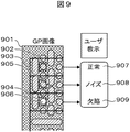
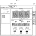
予めGP画像を取得し、GP画像に対して検査箇所及び閾値マップをGUI上で指定し、欠陥の識別基準を設定し、次に検査画像を取得し、検査画像に識別基準を適用し欠陥を識別することでパターン検査を行い高感度検査を可能にした。
【選択図】図1
Description
前記設定した欠陥識別基準を用いて前記作成したGP画像と検査画像との比較検査を行い、
該比較検査した結果を出力するようにした。
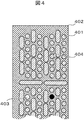
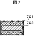
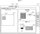
上記実施例では、メモリセル領域を撮像して得られたSEM画像をGP画像としているが、検出したい欠陥はメモリセル領域の特定の回路パターン部のみに発生する場合がある。この場合、検査画像とGP画像とをそのまま比較すると検出したくないノイズを欠陥候補として検出する可能性がある。例えば、図4に示すような穴401が並んでいる回路パターン402で、検出したい欠陥403はSEM画像上では穴の内側部分の明るさの違いであり、穴と穴との間の部分の明るさの違いは検出したくないノイズ404である場合が考えられる。そのまま比較するとノイズを欠陥候補として検出する可能性がある。
上記変形例1では、検出したい欠陥は検査箇所の明るさの違いであるとしたが、検査箇所が明るくなる(白くなる)場合は検出したい欠陥であるが、検査箇所が暗くなる(黒くなる)場合は検出したくないノイズの場合がある。そのまま比較するとノイズを欠陥候補として検出する可能性がある。
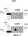
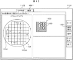
上記では、メモリマットが同じパターン形状のメモリセルの連続で構成されているものとしていたが、メモリセルのパターンとは異なる不規則パターンがメモリマットの中に含まれている場合がある。そのまま比較すると不規則パターンを欠陥候補として検出する可能性がある。
上記では、検出したい欠陥が発生する箇所がSEM画像上で明らかであるものとしていた。しかしながら、例えば、ダミーパターンのようにSEM画像上での見かけは実パターンと同様に見える形状でも、電気回路としては動作しないため、ダミーパターンで発生する欠陥候補は致命的でない場合がある。そのまま検査するとダミーパターンで欠陥を検出する可能性がある。
また、欠陥か否かはわかってもSEM画像上で差異が生じる箇所が明確でない場合がある。この場合、検査箇所をあいまい指定することになり、そのまま検査するとノイズを欠陥候補としたり、実欠陥を見逃す可能性がある。
上記では、検出したい欠陥は検査箇所の明るさの違いであるとしたが、検査箇所によっては検出したい欠陥の明るさレベルが異なる場合がある。そのまま比較すると検出したくない明るさレベルのノイズを欠陥候補として検出する可能性がある。
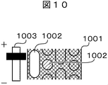
また、上記では、不規則パターン箇所を検査から除外する実施例を示したが、図10を用いて示した変形例6と同様に、不規則パターン箇所を別の検査箇所としてその欠陥検出閾値を、他の検査箇所の欠陥検出閾値と変えても良い。
Claims (12)
- 走査型電子顕微鏡(SEM)で取得した画像を用いて試料の欠陥を検査する方法であって、
SEMで取得した画像を用いてをGP画像を作成するステップと、
画面上で欠陥識別基準を設定するステップと、
前記SEMを用いて検査画像を取得するステップと、
前記設定した欠陥識別基準を用いて前記作成したGP画像と検査画像との比較検査を行うステップと、
該比較検査した結果を出力するステップと
を行うことを特徴とする欠陥検査方法。 - 前記GP画像を作成するステップにおいて、画面上で指定された検査対象試料上の領域を前記SEMで撮像し、該撮像して得た画像を用いてGP画像を作成することを特徴とする請求項1記載の欠陥検査方法。
- 前記GP画像を作成するステップにおいて、画面上で指定された検査対象試料上の領域を前記SEMで撮像し、該撮像して得た複数の画像を平均化して得られた画像からGP画像を作成することを特徴とする請求項1又は2に記載の欠陥検査方法。
- 欠陥識別基準を設定するステップにおいて、該欠陥識別基準を前記GP画像が表示されている画面上で設定することを特徴とする請求項1乃至3の何れかに記載の欠陥検査方法。
- 前記SEMを用いて検査画像を取得するステップにおいて、前記画面上で指定された領域又は前記画面上で指定された領域と同じ形状のパターンが形成された領域について前記SEMを用いて検査画像を取得することを特徴とする請求項1乃至3の何れかに記載の欠陥検査方法。
- 前記SEMを用いて検査画像を取得するステップにおいて、前記画面上で指定された領域又は前記画面上で指定された領域と同じ形状のパターンが形成された領域を除外して前記SEMを用いて検査画像を取得することを特徴とする請求項1乃至3の何れかに記載の欠陥検査方法。
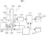
- 試料を撮像して該試料の画像を取得する走査型電子顕微鏡(SEM)手段と、
該SEM手段を用いて取得した試料の画像を表示する画面を有する表示手段と、
該表示手段に表示された前記試料の画像からGP画像を作成するGP画像作成手段と、
前記SEM手段を用いて取得した試料の画像から欠陥を識別するための欠陥識別基準を前記GP画像作成手段で作成されたGP画像が表示されている表示手段上で設定する欠陥識別基準設定手段と、
前記SEM手段を用いて前記試料を撮像して取得した画像を前記欠陥識別基準設定手段で設定した欠陥識別基準を用いて前記GP画像作成手段で作成したGP画像と比較検査して前記試料上の欠陥を検出する欠陥検出手段と、
該欠陥検出手段で前記試料上の欠陥を検出した結果を出力する出力手段と、
前記SEM手段と前記表示手段と前記GP画像作成手段と前記欠陥識別基準設定手段と前記欠陥検出手段と前記出力手段とを制御する制御手段と
を備えたことを特徴とする欠陥検査装置。 - 前記GP画像作成手段は、前記表示手段の画面上で指定された検査対象試料上の領域を前記SEMで撮像して得た画像からGP画像を作成することを特徴とする請求項7記載の欠陥検査装置。
- 前記GP画像作成手段は、前記表示手段の画面上で指定された検査対象試料上の領域を前記SEMで撮像して得た複数の画像を平均化して得られた画像からGP画像を作成することを特徴とする請求項7又は8に記載の欠陥検査装置。
- 欠陥識別基準設定手段は、前記GP画像作成手段で作成されたGP画像が表示されている前記表示手段の画面上で欠陥識別基準を設定することを特徴とする請求項7乃至9の何れかに記載の欠陥検査装置。
- 前記制御手段は、前記SEM手段を制御して、前記表示手段の画面上で指定された領域又は前記表示手段の画面上で指定された領域と同じ形状のパターンが形成された領域の検査画像を取得することを特徴とする請求項7乃至9の何れかに記載の欠陥検査装置。
- 前記制御手段は、前記SEM手段を制御して、前記表示手段の画面上で指定された領域又は前記表示手段の画面上で指定された領域と同じ形状のパターンが形成された領域を除外して検査画像を取得することを特徴とする請求項7乃至9の何れかに記載の欠陥検査装置。
Priority Applications (3)
| Application Number | Priority Date | Filing Date | Title |
|---|---|---|---|
| JP2010111126A JP5722551B2 (ja) | 2010-05-13 | 2010-05-13 | 欠陥検査方法及びその装置 |
| PCT/JP2011/058593 WO2011142196A1 (ja) | 2010-05-13 | 2011-04-05 | 欠陥検査方法及びその装置 |
| US13/697,025 US8853628B2 (en) | 2010-05-13 | 2011-04-05 | Defect inspection method, and device thereof |
Applications Claiming Priority (1)
| Application Number | Priority Date | Filing Date | Title |
|---|---|---|---|
| JP2010111126A JP5722551B2 (ja) | 2010-05-13 | 2010-05-13 | 欠陥検査方法及びその装置 |
Publications (2)
| Publication Number | Publication Date |
|---|---|
| JP2011237375A true JP2011237375A (ja) | 2011-11-24 |
| JP5722551B2 JP5722551B2 (ja) | 2015-05-20 |
Family
ID=44914252
Family Applications (1)
| Application Number | Title | Priority Date | Filing Date |
|---|---|---|---|
| JP2010111126A Active JP5722551B2 (ja) | 2010-05-13 | 2010-05-13 | 欠陥検査方法及びその装置 |
Country Status (3)
| Country | Link |
|---|---|
| US (1) | US8853628B2 (ja) |
| JP (1) | JP5722551B2 (ja) |
| WO (1) | WO2011142196A1 (ja) |
Cited By (6)
| Publication number | Priority date | Publication date | Assignee | Title |
|---|---|---|---|---|
| KR20150070301A (ko) * | 2012-10-15 | 2015-06-24 | 케이엘에이-텐코 코포레이션 | 결함 특유적 정보를 이용한 웨이퍼 상의 결함 검출 |
| JP2016507058A (ja) * | 2013-01-29 | 2016-03-07 | ケーエルエー−テンカー コーポレイション | パターン化された欠陥の輪郭ベースのアレイ検査 |
| JP2016524334A (ja) * | 2013-06-21 | 2016-08-12 | ケーエルエー−テンカー コーポレイション | 自由形態の保護領域を使用するウエハ検査 |
| JP2022545726A (ja) * | 2019-08-28 | 2022-10-28 | ケーエルエー コーポレイション | 走査型電子顕微法アプリケーション用センサモジュール |
| JPWO2023026489A1 (ja) * | 2021-08-27 | 2023-03-02 | ||
| CN118379602A (zh) * | 2024-06-25 | 2024-07-23 | 浙江大学 | 一种用语义和视觉解释增强半导体缺陷分析的方法和系统 |
Families Citing this family (10)
| Publication number | Priority date | Publication date | Assignee | Title |
|---|---|---|---|---|
| US10401305B2 (en) * | 2012-02-15 | 2019-09-03 | Kla-Tencor Corporation | Time-varying intensity map generation for reticles |
| US10146036B2 (en) | 2016-06-07 | 2018-12-04 | Globalfoundries Inc. | Semiconductor wafer inspection using care area group-specific threshold settings for detecting defects |
| JP7146367B2 (ja) * | 2017-01-30 | 2022-10-04 | オムロン株式会社 | 画像処理システム、情報処理装置、情報処理方法、および情報処理プログラム |
| DE102020125929A1 (de) * | 2020-05-06 | 2021-11-11 | Taiwan Semiconductor Manufacturing Co., Ltd. | Verfahren zur nicht destruktiven überprüfung parasitärer ätzabscheidungen auf zellen |
| US11749569B2 (en) * | 2020-05-06 | 2023-09-05 | Taiwan Semiconductor Manufacturing Company, Ltd. | Method for non-destructive inspection of cell etch redeposition |
| KR102836944B1 (ko) * | 2020-06-29 | 2025-07-22 | 삼성디스플레이 주식회사 | 마스크 검사 장치 및 마스크 검사 방법 |
| IT202100001718A1 (it) * | 2021-01-28 | 2022-07-28 | Getcoo S R L | Metodo di elaborazione di un'immagine di un oggetto e sistema per l'ispezione dell'oggetto. |
| EP4092614A1 (en) * | 2021-05-21 | 2022-11-23 | ASML Netherlands B.V. | Data processing device and method, charged particle assessment system and method |
| EP4341890A1 (en) * | 2021-05-21 | 2024-03-27 | ASML Netherlands B.V. | Data processing device and method, charged particle assessment system and method |
| US12362240B2 (en) * | 2022-07-28 | 2025-07-15 | Taiwan Semiconductor Manufacturing Company Ltd. | Method and system for detecting semiconductor device |
Citations (3)
| Publication number | Priority date | Publication date | Assignee | Title |
|---|---|---|---|---|
| JP2001304842A (ja) * | 2000-04-25 | 2001-10-31 | Hitachi Ltd | パターン検査方法及びその装置並びに基板の処理方法 |
| JP2008112690A (ja) * | 2006-10-31 | 2008-05-15 | Hitachi High-Technologies Corp | 走査型電子顕微鏡、および走査型電子顕微鏡を用いたパターンの複合検査方法 |
| WO2010029700A1 (ja) * | 2008-09-12 | 2010-03-18 | 株式会社日立ハイテクノロジーズ | 荷電粒子線装置 |
Family Cites Families (5)
| Publication number | Priority date | Publication date | Assignee | Title |
|---|---|---|---|---|
| US6898305B2 (en) | 2001-02-22 | 2005-05-24 | Hitachi, Ltd. | Circuit pattern inspection method and apparatus |
| JP4095860B2 (ja) * | 2002-08-12 | 2008-06-04 | 株式会社日立ハイテクノロジーズ | 欠陥検査方法及びその装置 |
| SG112082A1 (en) | 2003-11-10 | 2005-06-29 | Hermes Microvision Taiwan Inc | Method and system for monitoring ic process |
| KR100648201B1 (ko) * | 2005-08-08 | 2006-11-23 | 삼성전자주식회사 | 기판 검사 방법 및 이를 수행하기 위한 기판 검사 장치 |
| JP5075646B2 (ja) * | 2008-01-09 | 2012-11-21 | 株式会社日立ハイテクノロジーズ | 半導体欠陥検査装置ならびにその方法 |
-
2010
- 2010-05-13 JP JP2010111126A patent/JP5722551B2/ja active Active
-
2011
- 2011-04-05 US US13/697,025 patent/US8853628B2/en active Active
- 2011-04-05 WO PCT/JP2011/058593 patent/WO2011142196A1/ja not_active Ceased
Patent Citations (3)
| Publication number | Priority date | Publication date | Assignee | Title |
|---|---|---|---|---|
| JP2001304842A (ja) * | 2000-04-25 | 2001-10-31 | Hitachi Ltd | パターン検査方法及びその装置並びに基板の処理方法 |
| JP2008112690A (ja) * | 2006-10-31 | 2008-05-15 | Hitachi High-Technologies Corp | 走査型電子顕微鏡、および走査型電子顕微鏡を用いたパターンの複合検査方法 |
| WO2010029700A1 (ja) * | 2008-09-12 | 2010-03-18 | 株式会社日立ハイテクノロジーズ | 荷電粒子線装置 |
Cited By (12)
| Publication number | Priority date | Publication date | Assignee | Title |
|---|---|---|---|---|
| KR20150070301A (ko) * | 2012-10-15 | 2015-06-24 | 케이엘에이-텐코 코포레이션 | 결함 특유적 정보를 이용한 웨이퍼 상의 결함 검출 |
| JP2016502750A (ja) * | 2012-10-15 | 2016-01-28 | ケーエルエー−テンカー コーポレイション | 欠陥特定情報を用いるウェハ上の欠陥の検出 |
| KR20210034698A (ko) * | 2012-10-15 | 2021-03-30 | 케이엘에이 코포레이션 | 결함 특유적 정보를 이용한 웨이퍼 상의 결함 검출 |
| KR102233050B1 (ko) * | 2012-10-15 | 2021-03-30 | 케이엘에이 코포레이션 | 결함 특유적 정보를 이용한 웨이퍼 상의 결함 검출 |
| KR102379872B1 (ko) * | 2012-10-15 | 2022-03-30 | 케이엘에이 코포레이션 | 결함 특유적 정보를 이용한 웨이퍼 상의 결함 검출 |
| JP2016507058A (ja) * | 2013-01-29 | 2016-03-07 | ケーエルエー−テンカー コーポレイション | パターン化された欠陥の輪郭ベースのアレイ検査 |
| JP2016524334A (ja) * | 2013-06-21 | 2016-08-12 | ケーエルエー−テンカー コーポレイション | 自由形態の保護領域を使用するウエハ検査 |
| JP2022545726A (ja) * | 2019-08-28 | 2022-10-28 | ケーエルエー コーポレイション | 走査型電子顕微法アプリケーション用センサモジュール |
| JP7696888B2 (ja) | 2019-08-28 | 2025-06-23 | ケーエルエー コーポレイション | 走査型電子顕微法アプリケーション用センサモジュール |
| JPWO2023026489A1 (ja) * | 2021-08-27 | 2023-03-02 | ||
| JP7700248B2 (ja) | 2021-08-27 | 2025-06-30 | 株式会社日立ハイテク | コンピュータシステムおよび解析方法 |
| CN118379602A (zh) * | 2024-06-25 | 2024-07-23 | 浙江大学 | 一种用语义和视觉解释增强半导体缺陷分析的方法和系统 |
Also Published As
| Publication number | Publication date |
|---|---|
| WO2011142196A1 (ja) | 2011-11-17 |
| US20130119250A1 (en) | 2013-05-16 |
| JP5722551B2 (ja) | 2015-05-20 |
| US8853628B2 (en) | 2014-10-07 |
Similar Documents
| Publication | Publication Date | Title |
|---|---|---|
| JP5722551B2 (ja) | 欠陥検査方法及びその装置 | |
| KR101342203B1 (ko) | Sem을 이용한 결함 검사 방법 및 장치 | |
| US9311697B2 (en) | Inspection method and device therefor | |
| JP5006520B2 (ja) | 欠陥観察装置及び欠陥観察装置を用いた欠陥観察方法 | |
| TWI512684B (zh) | Defect observation method and defect observation device | |
| JP5325580B2 (ja) | Semを用いた欠陥観察方法及びその装置 | |
| JP4825469B2 (ja) | 半導体デバイスの欠陥レビュー方法及びその装置 | |
| US7932493B2 (en) | Method and system for observing a specimen using a scanning electron microscope | |
| KR102195029B1 (ko) | 결함 분류 장치 및 결함 분류 방법 | |
| KR101479889B1 (ko) | 하전 입자선 장치 | |
| JP5622398B2 (ja) | Semを用いた欠陥検査方法及び装置 | |
| JP2016139467A (ja) | 試料観察方法および試料観察装置 | |
| JP2016058465A (ja) | 欠陥定量化方法、欠陥定量化装置、および欠陥評価値表示装置 | |
| JP2008251766A (ja) | 半導体デバイスの欠陥観察方法及びその装置 | |
| US11211226B2 (en) | Pattern cross-sectional shape estimation system and program | |
| JP2012175101A (ja) | 限界寸法の測定、及び、製造均一性を監視する方法とシステム | |
| JP2005259396A (ja) | 欠陥画像収集方法およびその装置 | |
| JP2007067130A (ja) | 回路パターン検査方法及びその装置 | |
| JP2012169571A (ja) | 欠陥抽出走査電子顕微鏡検査装置及びその抽出方法 | |
| JP3836735B2 (ja) | 回路パターンの検査装置 | |
| US11087454B2 (en) | Defect observation device and defect observation method | |
| TWI824474B (zh) | 試料檢查裝置、檢查系統、薄片試料製作裝置及試料之檢查方法 | |
| JP5127411B2 (ja) | 走査型電子顕微鏡 | |
| JP6571045B2 (ja) | 荷電粒子ビーム装置及び荷電粒子ビーム装置を用いた画像の生成方法 |
Legal Events
| Date | Code | Title | Description |
|---|---|---|---|
| A621 | Written request for application examination |
Free format text: JAPANESE INTERMEDIATE CODE: A621 Effective date: 20120615 |
|
| A131 | Notification of reasons for refusal |
Free format text: JAPANESE INTERMEDIATE CODE: A131 Effective date: 20130507 |
|
| A521 | Request for written amendment filed |
Free format text: JAPANESE INTERMEDIATE CODE: A523 Effective date: 20130704 |
|
| A131 | Notification of reasons for refusal |
Free format text: JAPANESE INTERMEDIATE CODE: A131 Effective date: 20140311 |
|
| A521 | Request for written amendment filed |
Free format text: JAPANESE INTERMEDIATE CODE: A523 Effective date: 20140508 |
|
| A02 | Decision of refusal |
Free format text: JAPANESE INTERMEDIATE CODE: A02 Effective date: 20141007 |
|
| RD02 | Notification of acceptance of power of attorney |
Free format text: JAPANESE INTERMEDIATE CODE: A7422 Effective date: 20141027 |
|
| A521 | Request for written amendment filed |
Free format text: JAPANESE INTERMEDIATE CODE: A523 Effective date: 20141223 |
|
| A911 | Transfer to examiner for re-examination before appeal (zenchi) |
Free format text: JAPANESE INTERMEDIATE CODE: A911 Effective date: 20150108 |
|
| TRDD | Decision of grant or rejection written | ||
| A01 | Written decision to grant a patent or to grant a registration (utility model) |
Free format text: JAPANESE INTERMEDIATE CODE: A01 Effective date: 20150317 |
|
| A61 | First payment of annual fees (during grant procedure) |
Free format text: JAPANESE INTERMEDIATE CODE: A61 Effective date: 20150326 |
|
| R150 | Certificate of patent or registration of utility model |
Ref document number: 5722551 Country of ref document: JP Free format text: JAPANESE INTERMEDIATE CODE: R150 |
|
| S531 | Written request for registration of change of domicile |
Free format text: JAPANESE INTERMEDIATE CODE: R313531 |
|
| S533 | Written request for registration of change of name |
Free format text: JAPANESE INTERMEDIATE CODE: R313533 |
|
| R350 | Written notification of registration of transfer |
Free format text: JAPANESE INTERMEDIATE CODE: R350 |