WO2010024238A1 - Composition de résine, couche d’isolation de grille et transistor à couches minces organiques - Google Patents
Composition de résine, couche d’isolation de grille et transistor à couches minces organiques Download PDFInfo
- Publication number
- WO2010024238A1 WO2010024238A1 PCT/JP2009/064768 JP2009064768W WO2010024238A1 WO 2010024238 A1 WO2010024238 A1 WO 2010024238A1 JP 2009064768 W JP2009064768 W JP 2009064768W WO 2010024238 A1 WO2010024238 A1 WO 2010024238A1
- Authority
- WO
- WIPO (PCT)
- Prior art keywords
- group
- insulating layer
- film transistor
- gate insulating
- thin film
- Prior art date
Links
- 0 CCC(C)=NOC(NCCOC(C(C)(C*(C)C)C(C)C*(C)CC(C)(*CCC(C)(C)CC(*(C)C)c(c(F)c(c(F)c1F)F)c1F)C(OCC(F)(F)F)=O)=O)=O Chemical compound CCC(C)=NOC(NCCOC(C(C)(C*(C)C)C(C)C*(C)CC(C)(*CCC(C)(C)CC(*(C)C)c(c(F)c(c(F)c1F)F)c1F)C(OCC(F)(F)F)=O)=O)=O 0.000 description 1
- XRRZUFHVEGUSBS-UHFFFAOYSA-N CCC(CCC(C)(CC1c2c(cc3F)[F]C1(C)C)[F]c2c3F)c(cc1)ccc1N Chemical compound CCC(CCC(C)(CC1c2c(cc3F)[F]C1(C)C)[F]c2c3F)c(cc1)ccc1N XRRZUFHVEGUSBS-UHFFFAOYSA-N 0.000 description 1
Images

Classifications
-
- C—CHEMISTRY; METALLURGY
- C08—ORGANIC MACROMOLECULAR COMPOUNDS; THEIR PREPARATION OR CHEMICAL WORKING-UP; COMPOSITIONS BASED THEREON
- C08F—MACROMOLECULAR COMPOUNDS OBTAINED BY REACTIONS ONLY INVOLVING CARBON-TO-CARBON UNSATURATED BONDS
- C08F220/00—Copolymers of compounds having one or more unsaturated aliphatic radicals, each having only one carbon-to-carbon double bond, and only one being terminated by only one carboxyl radical or a salt, anhydride ester, amide, imide or nitrile thereof
- C08F220/02—Monocarboxylic acids having less than ten carbon atoms; Derivatives thereof
- C08F220/10—Esters
- C08F220/22—Esters containing halogen
-
- C—CHEMISTRY; METALLURGY
- C08—ORGANIC MACROMOLECULAR COMPOUNDS; THEIR PREPARATION OR CHEMICAL WORKING-UP; COMPOSITIONS BASED THEREON
- C08F—MACROMOLECULAR COMPOUNDS OBTAINED BY REACTIONS ONLY INVOLVING CARBON-TO-CARBON UNSATURATED BONDS
- C08F12/00—Homopolymers and copolymers of compounds having one or more unsaturated aliphatic radicals, each having only one carbon-to-carbon double bond, and at least one being terminated by an aromatic carbocyclic ring
- C08F12/02—Monomers containing only one unsaturated aliphatic radical
- C08F12/04—Monomers containing only one unsaturated aliphatic radical containing one ring
- C08F12/14—Monomers containing only one unsaturated aliphatic radical containing one ring substituted by hetero atoms or groups containing heteroatoms
- C08F12/16—Halogens
- C08F12/20—Fluorine
-
- C—CHEMISTRY; METALLURGY
- C08—ORGANIC MACROMOLECULAR COMPOUNDS; THEIR PREPARATION OR CHEMICAL WORKING-UP; COMPOSITIONS BASED THEREON
- C08F—MACROMOLECULAR COMPOUNDS OBTAINED BY REACTIONS ONLY INVOLVING CARBON-TO-CARBON UNSATURATED BONDS
- C08F12/00—Homopolymers and copolymers of compounds having one or more unsaturated aliphatic radicals, each having only one carbon-to-carbon double bond, and at least one being terminated by an aromatic carbocyclic ring
- C08F12/02—Monomers containing only one unsaturated aliphatic radical
- C08F12/04—Monomers containing only one unsaturated aliphatic radical containing one ring
- C08F12/14—Monomers containing only one unsaturated aliphatic radical containing one ring substituted by hetero atoms or groups containing heteroatoms
- C08F12/22—Oxygen
- C08F12/24—Phenols or alcohols
-
- C—CHEMISTRY; METALLURGY
- C08—ORGANIC MACROMOLECULAR COMPOUNDS; THEIR PREPARATION OR CHEMICAL WORKING-UP; COMPOSITIONS BASED THEREON
- C08F—MACROMOLECULAR COMPOUNDS OBTAINED BY REACTIONS ONLY INVOLVING CARBON-TO-CARBON UNSATURATED BONDS
- C08F212/00—Copolymers of compounds having one or more unsaturated aliphatic radicals, each having only one carbon-to-carbon double bond, and at least one being terminated by an aromatic carbocyclic ring
- C08F212/02—Monomers containing only one unsaturated aliphatic radical
- C08F212/04—Monomers containing only one unsaturated aliphatic radical containing one ring
- C08F212/06—Hydrocarbons
- C08F212/08—Styrene
- C08F212/10—Styrene with nitriles
-
- C—CHEMISTRY; METALLURGY
- C08—ORGANIC MACROMOLECULAR COMPOUNDS; THEIR PREPARATION OR CHEMICAL WORKING-UP; COMPOSITIONS BASED THEREON
- C08F—MACROMOLECULAR COMPOUNDS OBTAINED BY REACTIONS ONLY INVOLVING CARBON-TO-CARBON UNSATURATED BONDS
- C08F212/00—Copolymers of compounds having one or more unsaturated aliphatic radicals, each having only one carbon-to-carbon double bond, and at least one being terminated by an aromatic carbocyclic ring
- C08F212/02—Monomers containing only one unsaturated aliphatic radical
- C08F212/04—Monomers containing only one unsaturated aliphatic radical containing one ring
- C08F212/14—Monomers containing only one unsaturated aliphatic radical containing one ring substituted by heteroatoms or groups containing heteroatoms
- C08F212/16—Halogens
- C08F212/20—Fluorine
-
- C—CHEMISTRY; METALLURGY
- C08—ORGANIC MACROMOLECULAR COMPOUNDS; THEIR PREPARATION OR CHEMICAL WORKING-UP; COMPOSITIONS BASED THEREON
- C08F—MACROMOLECULAR COMPOUNDS OBTAINED BY REACTIONS ONLY INVOLVING CARBON-TO-CARBON UNSATURATED BONDS
- C08F212/00—Copolymers of compounds having one or more unsaturated aliphatic radicals, each having only one carbon-to-carbon double bond, and at least one being terminated by an aromatic carbocyclic ring
- C08F212/02—Monomers containing only one unsaturated aliphatic radical
- C08F212/04—Monomers containing only one unsaturated aliphatic radical containing one ring
- C08F212/14—Monomers containing only one unsaturated aliphatic radical containing one ring substituted by heteroatoms or groups containing heteroatoms
- C08F212/22—Oxygen
- C08F212/24—Phenols or alcohols
-
- C—CHEMISTRY; METALLURGY
- C08—ORGANIC MACROMOLECULAR COMPOUNDS; THEIR PREPARATION OR CHEMICAL WORKING-UP; COMPOSITIONS BASED THEREON
- C08F—MACROMOLECULAR COMPOUNDS OBTAINED BY REACTIONS ONLY INVOLVING CARBON-TO-CARBON UNSATURATED BONDS
- C08F220/00—Copolymers of compounds having one or more unsaturated aliphatic radicals, each having only one carbon-to-carbon double bond, and only one being terminated by only one carboxyl radical or a salt, anhydride ester, amide, imide or nitrile thereof
- C08F220/02—Monocarboxylic acids having less than ten carbon atoms; Derivatives thereof
- C08F220/10—Esters
- C08F220/12—Esters of monohydric alcohols or phenols
- C08F220/16—Esters of monohydric alcohols or phenols of phenols or of alcohols containing two or more carbon atoms
- C08F220/18—Esters of monohydric alcohols or phenols of phenols or of alcohols containing two or more carbon atoms with acrylic or methacrylic acids
- C08F220/1802—C2-(meth)acrylate, e.g. ethyl (meth)acrylate
-
- C—CHEMISTRY; METALLURGY
- C08—ORGANIC MACROMOLECULAR COMPOUNDS; THEIR PREPARATION OR CHEMICAL WORKING-UP; COMPOSITIONS BASED THEREON
- C08F—MACROMOLECULAR COMPOUNDS OBTAINED BY REACTIONS ONLY INVOLVING CARBON-TO-CARBON UNSATURATED BONDS
- C08F220/00—Copolymers of compounds having one or more unsaturated aliphatic radicals, each having only one carbon-to-carbon double bond, and only one being terminated by only one carboxyl radical or a salt, anhydride ester, amide, imide or nitrile thereof
- C08F220/02—Monocarboxylic acids having less than ten carbon atoms; Derivatives thereof
- C08F220/10—Esters
- C08F220/34—Esters containing nitrogen, e.g. N,N-dimethylaminoethyl (meth)acrylate
- C08F220/36—Esters containing nitrogen, e.g. N,N-dimethylaminoethyl (meth)acrylate containing oxygen in addition to the carboxy oxygen, e.g. 2-N-morpholinoethyl (meth)acrylate or 2-isocyanatoethyl (meth)acrylate
-
- C—CHEMISTRY; METALLURGY
- C08—ORGANIC MACROMOLECULAR COMPOUNDS; THEIR PREPARATION OR CHEMICAL WORKING-UP; COMPOSITIONS BASED THEREON
- C08K—Use of inorganic or non-macromolecular organic substances as compounding ingredients
- C08K5/00—Use of organic ingredients
- C08K5/0008—Organic ingredients according to more than one of the "one dot" groups of C08K5/01 - C08K5/59
- C08K5/0025—Crosslinking or vulcanising agents; including accelerators
-
- C—CHEMISTRY; METALLURGY
- C08—ORGANIC MACROMOLECULAR COMPOUNDS; THEIR PREPARATION OR CHEMICAL WORKING-UP; COMPOSITIONS BASED THEREON
- C08L—COMPOSITIONS OF MACROMOLECULAR COMPOUNDS
- C08L25/00—Compositions of, homopolymers or copolymers of compounds having one or more unsaturated aliphatic radicals, each having only one carbon-to-carbon double bond, and at least one being terminated by an aromatic carbocyclic ring; Compositions of derivatives of such polymers
- C08L25/18—Homopolymers or copolymers of aromatic monomers containing elements other than carbon and hydrogen
-
- H—ELECTRICITY
- H10—SEMICONDUCTOR DEVICES; ELECTRIC SOLID-STATE DEVICES NOT OTHERWISE PROVIDED FOR
- H10K—ORGANIC ELECTRIC SOLID-STATE DEVICES
- H10K10/00—Organic devices specially adapted for rectifying, amplifying, oscillating or switching; Organic capacitors or resistors having a potential-jump barrier or a surface barrier
- H10K10/40—Organic transistors
- H10K10/46—Field-effect transistors, e.g. organic thin-film transistors [OTFT]
- H10K10/462—Insulated gate field-effect transistors [IGFETs]
- H10K10/468—Insulated gate field-effect transistors [IGFETs] characterised by the gate dielectrics
- H10K10/471—Insulated gate field-effect transistors [IGFETs] characterised by the gate dielectrics the gate dielectric comprising only organic materials
-
- C—CHEMISTRY; METALLURGY
- C08—ORGANIC MACROMOLECULAR COMPOUNDS; THEIR PREPARATION OR CHEMICAL WORKING-UP; COMPOSITIONS BASED THEREON
- C08F—MACROMOLECULAR COMPOUNDS OBTAINED BY REACTIONS ONLY INVOLVING CARBON-TO-CARBON UNSATURATED BONDS
- C08F220/00—Copolymers of compounds having one or more unsaturated aliphatic radicals, each having only one carbon-to-carbon double bond, and only one being terminated by only one carboxyl radical or a salt, anhydride ester, amide, imide or nitrile thereof
- C08F220/02—Monocarboxylic acids having less than ten carbon atoms; Derivatives thereof
- C08F220/10—Esters
- C08F220/34—Esters containing nitrogen, e.g. N,N-dimethylaminoethyl (meth)acrylate
- C08F220/343—Esters containing nitrogen, e.g. N,N-dimethylaminoethyl (meth)acrylate in the form of urethane links
-
- C—CHEMISTRY; METALLURGY
- C08—ORGANIC MACROMOLECULAR COMPOUNDS; THEIR PREPARATION OR CHEMICAL WORKING-UP; COMPOSITIONS BASED THEREON
- C08L—COMPOSITIONS OF MACROMOLECULAR COMPOUNDS
- C08L2205/00—Polymer mixtures characterised by other features
- C08L2205/02—Polymer mixtures characterised by other features containing two or more polymers of the same C08L -group
-
- H—ELECTRICITY
- H10—SEMICONDUCTOR DEVICES; ELECTRIC SOLID-STATE DEVICES NOT OTHERWISE PROVIDED FOR
- H10K—ORGANIC ELECTRIC SOLID-STATE DEVICES
- H10K10/00—Organic devices specially adapted for rectifying, amplifying, oscillating or switching; Organic capacitors or resistors having a potential-jump barrier or a surface barrier
- H10K10/40—Organic transistors
- H10K10/46—Field-effect transistors, e.g. organic thin-film transistors [OTFT]
- H10K10/462—Insulated gate field-effect transistors [IGFETs]
- H10K10/464—Lateral top-gate IGFETs comprising only a single gate
-
- H—ELECTRICITY
- H10—SEMICONDUCTOR DEVICES; ELECTRIC SOLID-STATE DEVICES NOT OTHERWISE PROVIDED FOR
- H10K—ORGANIC ELECTRIC SOLID-STATE DEVICES
- H10K10/00—Organic devices specially adapted for rectifying, amplifying, oscillating or switching; Organic capacitors or resistors having a potential-jump barrier or a surface barrier
- H10K10/40—Organic transistors
- H10K10/46—Field-effect transistors, e.g. organic thin-film transistors [OTFT]
- H10K10/462—Insulated gate field-effect transistors [IGFETs]
- H10K10/466—Lateral bottom-gate IGFETs comprising only a single gate
Definitions
- the present invention relates to a resin composition, and more particularly to a resin composition for an organic thin film transistor gate insulating layer.
- Organic field effect transistors can be manufactured at a lower temperature than inorganic semiconductors, so that a plastic substrate or film can be used as a substrate, and an element that is light and difficult to break can be manufactured.
- an element can be manufactured by application of a solution containing an organic material or film formation using a printing method, and thus a large-area element can be manufactured at low cost.
- material characteristics can be easily changed. Therefore, by combining materials having different functions, it is possible to realize various and flexible functions, elements, and the like that are impossible with inorganic semiconductors.
- the voltage applied to the gate electrode acts on the semiconductor layer through the gate insulating layer to control on / off of the drain current.
- the gate insulating layer material used for the organic field effect transistor is required to have excellent insulating properties and excellent breakdown strength when formed into a thin film.
- a semiconductor layer is formed so as to overlap with a gate insulating layer. Therefore, the gate insulating layer material is also required to have characteristics such as affinity with the organic semiconductor for forming a good interface with the organic semiconductor and flatness of the film surface forming the interface with the semiconductor.
- Patent Document 1 describes that an epoxy resin and a silane coupling agent are used in combination as a gate insulating layer material in an organic thin film transistor. Since the gate insulating layer material has high hygroscopicity, there is a problem in the stability of the transistor performance. To solve this problem, the hydroxyl group generated during the curing reaction of the epoxy resin was reacted with the silane coupling agent. Is.
- Non-Patent Document 1 describes that a resin obtained by thermally cross-linking polyvinylphenol and a melamine compound is used for the gate insulating layer. By crosslinking with a melamine compound, the hydroxyl group contained in polyvinylphenol is removed, and at the same time the film strength is increased.
- the pentacene TFT having this gate insulating layer has a small hysteresis and exhibits durability against gate bias stress.
- Non-Patent Document 2 describes that polyvinyl gate and a copolymer obtained by copolymerizing vinyl phenol and methyl methacrylate are used for the gate insulating layer. The polarity of the whole film is lowered by interacting the hydroxyl group of vinylphenol with the carbonyl group of methyl methacrylate. The pentacene TFT having this gate insulating layer has a small hysteresis and exhibits stable electrical characteristics.
- organic electroluminescence element organic electroluminescence element
- An object of the present invention is to provide an organic thin film transistor having a small hysteresis.
- the contact angle of the gate insulating layer with respect to pure water is preferably 91 degrees or more, more preferably 91 degrees or more and 110 degrees or less. If this contact angle exceeds 110 degrees, the affinity with the organic material and the metal tends to deteriorate, and it may be difficult to form the organic layer and the wiring layer in contact with the exposed surface of the insulating layer.
- the contact angle of the gate insulating layer of the present invention with respect to pure water is 91 to 100 degrees, more preferably 92 to 96 degrees.
- a resin composition useful for forming such a gate insulating layer is a resin composition containing a specific polymer compound containing a fluorine atom and capable of forming a crosslinked structure.
- the present invention is selected from the group consisting of (A) a repeating unit represented by the general formula (1), a repeating unit represented by the general formula (1 ′), and a repeating unit represented by the general formula (2).
- a high molecular compound that is a functional group that generates a second functional group that reacts with hydrogen (B) a low molecular compound containing two or more active hydrogens in the molecule, and two or more active hydrogens in the molecule
- a resin composition containing at least one compound selected from the group consisting of polymer compounds.
- R 1 , R 2 and R 3 are the same or different and each represents a hydrogen atom, a fluorine atom or a monovalent organic group having 1 to 20 carbon atoms.
- R is a hydrogen atom or 1 to 20 carbon atoms
- a hydrogen atom in the monovalent organic group may be substituted with a fluorine atom
- Raa represents a divalent organic group having 1 to 20 carbon atoms.
- the hydrogen atom in the valent organic group may be substituted with a fluorine atom
- a represents an integer of 0 to 20
- b represents an integer of 1 to 5.
- R ′ 1 , R ′ 2 and R ′ 3 are the same or different and each represents a hydrogen atom, a fluorine atom or a monovalent organic group having 1 to 20 carbon atoms.
- R ′ represents at least one
- a hydrogen atom is a monovalent organic group having 1 to 20 carbon atoms substituted with a fluorine atom
- R′aa represents a divalent organic group having 1 to 20 carbon atoms.
- a hydrogen atom may be substituted with a fluorine atom
- a ′ represents an integer of 0 to 20
- b ′ represents an integer of 1 to 5.
- R 4 , R 5 and R 6 are the same or different and each represents a hydrogen atom, a fluorine atom or a monovalent organic group having 1 to 20 carbon atoms.
- the hydrogen atom in the monovalent organic group is Rf represents a monovalent organic group having 1 to 20 carbon atoms in which at least one hydrogen atom has been replaced with a fluorine atom, and Rbb represents one having 1 to 20 carbon atoms.
- Rf represents a monovalent organic group having 1 to 20 carbon atoms in which at least one hydrogen atom has been replaced with a fluorine atom
- Rbb represents one having 1 to 20 carbon atoms.
- c represents an integer of 0 to 20.
- the said resin composition is for organic thin-film transistor gate insulating layers.
- the first functional group is at least one group selected from the group consisting of an isocyanato group blocked with a blocking agent and an isothiocyanato group blocked with a blocking agent.
- the isocyanato group blocked with the blocking agent is a group represented by the general formula (3).
- R 7 and R 8 are the same or different and represent a hydrogen atom or a monovalent organic group having 1 to 20 carbon atoms.
- the isothiocyanato group blocked with the blocking agent is a group represented by the general formula (4).
- X represents an oxygen atom or a sulfur atom
- R 9 , R 10 and R 11 are the same or different and each represents a hydrogen atom or a monovalent organic group having 1 to 20 carbon atoms.
- the present invention provides a gate insulating layer of an organic thin film transistor formed using any of the above resin compositions.
- the gate insulating layer of the organic thin film transistor has a contact angle with respect to pure water of 91 degrees or more.
- the present invention provides an organic thin film transistor having the gate insulating layer.
- the present invention provides the organic thin film transistor of the bottom gate top contact type or the bottom gate bottom contact type.
- the present invention provides a display member including the organic thin film transistor.
- the present invention provides a display including the display member.
- the gate insulating layer of the present invention polarization at the gate insulating layer interface is suppressed even when a gate voltage is applied. As a result, the hysteresis of the organic field effect transistor is lowered. In addition, since there are few polar groups on the surface of the gate insulating layer, formation of carrier trap order is suppressed. As a result, the absolute value of Vth of the organic field effect transistor decreases.
- the “polymer compound” refers to a compound having a structure in which a plurality of the same structural units are repeated in the molecule, and includes a so-called dimer.
- the “low molecular compound” means a compound that does not have the same structural unit repeatedly in the molecule.
- the resin composition for a gate insulating layer according to the present invention has a polymer compound (A) having a plurality of functional groups that react with active hydrogen when electromagnetic waves or heat acts, and a fluorine atom introduced, and active in the molecule.
- An active hydrogen compound (B) having a plurality of hydrogen is contained.
- Active hydrogen refers to a hydrogen atom bonded to an atom other than a carbon atom such as an oxygen atom, a nitrogen atom and a sulfur atom.
- Polymer compound (A) The polymer compound (A) has a fluorine-substituted organic moiety, for example, a repeating unit containing a fluorine atom.
- a preferred repeating unit is selected from the group consisting of the repeating unit represented by the general formula (1), the repeating unit represented by the general formula (1 ′), and the repeating unit represented by the general formula (2). At least one.
- R 1 to R 6 and R ′ 1 to R ′ 3 are the same or different and are a hydrogen atom, a fluorine atom or a carbon atom.
- a hydrogen atom in the monovalent organic group may be substituted with a fluorine atom.
- R 1 to R 6 and R ′ 1 to R ′ 3 are all hydrogen atoms, or R 4 is a methyl group, R 1 to R 3 , R 5 and R 6, and R ′ 1 to R ′ 3.
- Raa, R'aa and Rbb represent a divalent organic group having 1 to 20 carbon atoms.
- a hydrogen atom in the divalent organic group may be substituted with a fluorine atom.
- a, a ′ and c each represents an integer of 0 to 20. In one certain form, a, a ', and c are 0.
- R represents a hydrogen atom or a monovalent organic group having 1 to 20 carbon atoms.
- a hydrogen atom in the monovalent organic group may be substituted with a fluorine atom.
- R ′ represents a monovalent organic group having 1 to 20 carbon atoms in which at least one hydrogen atom is substituted with a fluorine atom.
- b and b 'each represents an integer of 1 to 5. In one embodiment, b is 5 and b 'is 1.
- Rf represents a monovalent organic group having 1 to 20 carbon atoms in which at least one hydrogen atom is substituted with a fluorine atom.
- Rf is a 2,2,2-trifluoroethyl group, a 2,2,3,3,3-pentafluoropropyl group, or a 2- (perfluorobutyl) ethyl group.
- the monovalent organic group having 1 to 20 carbon atoms may be linear, branched or cyclic, and may be saturated or unsaturated.
- Examples of the monovalent organic group having 1 to 20 carbon atoms include a linear hydrocarbon group having 1 to 20 carbon atoms, a branched hydrocarbon group having 3 to 20 carbon atoms, and a cyclic hydrocarbon having 3 to 20 carbon atoms.
- a hydrogen atom in the group may be substituted with an alkyl group, a halogen atom or the like.
- the monovalent organic group having 1 to 20 carbon atoms include methyl group, ethyl group, propyl group, butyl group, pentyl group, hexyl group, isopropyl group, isobutyl group, tertiary butyl group, cyclopropyl group, Cyclobutyl group, cyclopentyl group, cyclohexyl group, cyclopentynyl group, cyclohexynyl group, trifluoromethyl group, trifluoroethyl group, phenyl group, naphthyl group, anthryl group, tolyl group, xylyl group, dimethylphenyl group, trimethylphenyl group , Ethylphenyl group, diethylphenyl group, triethylphenyl group, propylphenyl group, butylphenyl group, methylnaphthyl group, dimethylnaphthyl group,
- the divalent organic group having 1 to 20 carbon atoms may be linear, branched or cyclic, and examples thereof include a linear aliphatic hydrocarbon group having 1 to 20 carbon atoms and 3 to 3 carbon atoms. 20 branched aliphatic hydrocarbon groups, cyclic aliphatic hydrocarbon groups having 3 to 20 carbon atoms, aromatic hydrocarbon groups having 6 to 20 carbon atoms which may be substituted with alkyl groups, and the like.
- Aromatic hydrocarbon groups are preferred.
- aliphatic hydrocarbon group examples include methylene group, ethylene group, propylene group, butylene group, pentylene group, hexylene group, isopropylene group, isobutylene group, dimethylpropylene group, cyclopropylene group, cyclobutylene group, cyclohexane.
- a pentylene group, a cyclohexylene group, etc. are mentioned.
- aromatic hydrocarbon group having 6 to 20 carbon atoms include phenylene group, naphthylene group, anthrylene group, dimethylphenylene group, trimethylphenylene group, ethylenephenylene group, diethylenephenylene group, triethylenephenylene group, propylenephenylene group.
- Preferred examples of the repeating unit represented by the formula (1), the repeating unit represented by the formula (1 ′) and the repeating unit represented by the formula (2) are the following repeating units.
- the polymer compound (A) has a functional group that reacts with active hydrogen when electromagnetic waves or heat acts.
- the functional group of the polymer compound (A) is the first functional group
- the first functional group does not react with active hydrogen, but electromagnetic waves or heat acts on the first functional group.
- a second functional group is generated and reacts with active hydrogen. That is, the first functional group is a functional group that is deprotected by electromagnetic waves or heat to generate a second functional group that reacts with active hydrogen.
- the second functional group is protected (blocked) until an electromagnetic wave or heat is applied in the step of forming the gate insulating layer, and is present in the resin composition as the first functional group.
- the storage stability of the resin composition is improved.
- Examples of the first functional group include an isocyanato group blocked with a blocking agent or an isothiocyanato group blocked with a blocking agent.
- the isocyanate group blocked with the blocking agent or the blocked isothiocyanato group reacts with a blocking agent having only one active hydrogen capable of reacting with the isocyanato group or isothiocyanato group with the isocyanato group or isothiocyanato group.
- the blocking agent is preferably one that dissociates at a temperature of 170 ° C. or lower even after reacting with an isocyanato group or an isothiocyanato group.
- the blocking agent include alcohol compounds, phenol compounds, active methylene compounds, mercaptan compounds, acid amide compounds, acid imide compounds, imidazole compounds, urea compounds, and oxime compounds.
- an oxime type compound and a pyrazole type compound are mentioned.
- the blocking agent include alcohol compounds such as methanol, ethanol, propanol, butanol, 2-ethylhexanol, methyl cellosolve, butyl cellosolve, methyl carbitol, benzyl alcohol, and cyclohexanol.
- alcohol compounds such as methanol, ethanol, propanol, butanol, 2-ethylhexanol, methyl cellosolve, butyl cellosolve, methyl carbitol, benzyl alcohol, and cyclohexanol.
- phenolic compounds include phenol, cresol, ethylphenol, butylphenol, nonylphenol, dinonylphenol, styrenated phenol, hydroxybenzoic acid ester, and the like.
- active methylene compound include dimethyl malonate, diethyl malonate, methyl acetoacetate, ethyl acetoacetate, and acetylacetone.
- Examples of mercaptan compounds include butyl mercaptan and dodecyl mercaptan.
- acid amide compounds include acetanilide, acetic acid amide, ⁇ -caprolactam, ⁇ -valerolactam, and ⁇ -butyrolactam.
- acid imide compounds include succinimide and maleic imide.
- Examples of the imidazole compound include imidazole and 2-methylimidazole.
- Examples of urea compounds include urea, thiourea, and ethylene urea.
- Examples of the amine compound include diphenylamine, aniline, carbazole and the like.
- Examples of the imine compound include ethyleneimine and polyethyleneimine.
- Examples of the bisulfite include sodium bisulfite.
- Examples of pyridine compounds include 2-hydroxypyridine and 2-hydroxyquinoline.
- Examples of oxime compounds include formal oxime, acetal oxime, acetoxime, methyl ethyl ketoxime, cyclohexanone oxime, and the like.
- Examples of the pyrazole compound include 3,5-dimethylpyrazole, 3,5-diethylpyrazole and the like.
- the isocyanato group or isothiocyanato group blocked with a blocking agent that may be used in the present invention is preferably a group represented by the following general formula (3) or general formula (4).
- X represents an oxygen atom or a sulfur atom
- R 7 to R 11 are the same or different and each represents a hydrogen atom or a monovalent organic group having 1 to 20 carbon atoms.
- the definition and specific examples of the monovalent organic group are the same as the definition and specific examples of the monovalent organic group in R 1 to R 6 described above.
- R 7 and R 8 are each independently a group selected from the group consisting of a methyl group and an ethyl group, and R 9 to R 11 are hydrogen atoms.
- Examples of the isocyanato group blocked with a blocking agent include O- (methylideneamino) carboxyamino group, O- (1-ethylideneamino) carboxyamino group, O- (1-methylethylideneamino) carboxyamino group, O— [1-methylpropylideneamino] carboxyamino group, (N-3,5-dimethylpyrazolylcarbonyl) amino group, (N-3-ethyl-5-methylpyrazolylcarbonyl) amino group, (N-3,5-diethyl) And pyrazolylcarbonyl) amino group, (N-3-propyl-5-methylpyrazolylcarbonyl) amino group, and (N-3-ethyl-5-propylpyrazolylcarbonyl) amino group.
- Examples of the isothiocyanato group blocked with a blocking agent include an O- (methylideneamino) thiocarboxyamino group, an O- (1-ethylideneamino) thiocarboxyamino group, and an O- (1-methylethylideneamino) thiocarboxyamino group.
- the first functional group used in the present invention is preferably an isocyanato group blocked with a blocking agent.
- the polymer compound (A) is, for example, a polymerizable monomer that is a raw material of the repeating unit represented by the general formula (1) or a polysynthetic monomer that is a raw material of the repeating unit represented by the general formula (1 ′);
- a method of copolymerizing a polymerizable monomer serving as a raw material of the repeating unit represented by the general formula (2) and a polymerizable monomer containing the first functional group using a photopolymerization initiator or a thermal polymerization initiator. can be manufactured.
- the polymerizable monomer that is a raw material of the repeating unit represented by the general formula (1), and the polysynthetic monomer that is a raw material of the repeating unit represented by the general formula (1 ′) include 4-trifluoromethylstyrene, 2, Examples include 3,4,5,6-pentafluorostyrene, 4-fluoromethylstyrene and the like.
- Examples of the polymerizable monomer that is a raw material for the repeating unit represented by the general formula (2) include 2,2,2-trifluoroethyl acrylate, 2,2,3,3,3-pentafluoropropyl acrylate, 2- ( Perfluorobutyl) ethyl acrylate, 3-perfluorobutyl-2-hydroxypropyl acrylate, 2- (perfluorohexyl) ethyl acrylate, 3-perfluorohexyl-2-hydroxypropyl acrylate, 2- (perfluorooctyl) ethyl acrylate 3-perfluorooctyl-2-hydroxypropyl acrylate, 2- (perfluorodecyl) ethyl acrylate, 2- (perfluoro-3-methylbutyl) ethyl acrylate, 3- (perfluoro-3-methylbutyl) -2-hydroxy Propyl-Ak Relate, 2- (perfluoro-5-methyl
- Examples of the polymerizable monomer containing the first functional group include a monomer having an isocyanato group blocked with a blocking agent or an isothiocyanato group blocked with a blocking agent and an unsaturated bond in the molecule.
- a monomer having an isocyanato group blocked with the blocking agent or an isothiocyanato group blocked with a blocking agent and an unsaturated bond in the molecule is an isocyanate group or a compound having an isothiocyanato group and an unsaturated bond in the molecule. It can be produced by reacting with a blocking agent.
- As the unsaturated bond an unsaturated double bond is preferable.
- Examples of the compound having an unsaturated double bond and an isocyanato group in the molecule include 2-acryloyloxyethyl isocyanate, 2-methacryloyloxyethyl isocyanate, 2- (2'-methacryloyloxyethyl) oxyethyl isocyanate, and the like.
- Examples of the compound having an unsaturated double bond and an isothiocyanato group in the molecule include 2-acryloyloxyethyl isothiocyanate, 2-methacryloyloxyethyl isothiocyanate, 2- (2′-methacryloyloxyethyl) oxyethyl isothiocyanate, and the like. It is done.
- the above blocking agents can be suitably used, and an organic solvent, a catalyst, or the like can be added as necessary.
- Examples of the monomer having an unsaturated double bond and an isocyanato group blocked with a blocking agent in the molecule include 2- [O- [1′-methylpropylideneamino] carboxyamino] ethyl methacrylate, 2- [N -[1 ', 3'-dimethylpyrazolyl] carboxyamino] ethyl-methacrylate and the like.
- photopolymerization initiator examples include acetophenone, 2,2-dimethoxy-2-phenylacetophenone, 2,2-diethoxyacetophenone, 4-isopropyl-2-hydroxy-2-methylpropiophenone, 2-hydroxy- 2-methylpropiophenone, 4,4′-bis (diethylamino) benzophenone, benzophenone, methyl (o-benzoyl) benzoate, 1-phenyl-1,2-propanedione-2- (o-ethoxycarbonyl) oxime, -Phenyl-1,2-propanedione-2- (o-benzoyl) oxime, benzoin, benzoin methyl ether, benzoin ethyl ether, benzoin isopropyl ether, benzoin isobutyl ether, benzoin octyl ether, benzyl, benzyldimethyl Ketal, benzyl diethyl ketal, carbonyl compounds di
- the thermal polymerization initiator may be any radical polymerization initiator, such as 2,2′-azobisisobutyronitrile, 2,2′-azobisisovaleronitrile, 2,2 ′. -Azobis (2,4-dimethylvaleronitrile), 4,4'-azobis (4-cyanovaleric acid), 1,1'-azobis (cyclohexanecarbonitrile), 2,2'-azobis (2-methylpropane) ), Azo compounds such as 2,2′-azobis (2-methylpropionamidine) dihydrochloride, ketone peroxides such as methyl ethyl ketone peroxide, methyl isobutyl ketone peroxide, cyclohexanone peroxide, acetylacetone peroxide, isobutyl peroxide Oxide, benzoyl peroxide, 2,4-dichlorobenzoyl peroxy Diacyl peroxides such as o-methylbenzoyl peroxide, lau
- the polymer compound used in the present invention includes a polymerizable monomer that is a raw material for the repeating unit represented by the general formula (1), and a polysynthetic monomer that is a raw material for the repeating unit represented by the general formula (1 ′).
- a polymerizable monomer other than the polymerizable monomer serving as the raw material of the repeating unit represented by the general formula (2) and the polymerizable monomer containing the first functional group may be added during the polymerization. .
- Examples of the other polymerizable monomers include acrylic acid esters and derivatives thereof, methacrylic acid esters and derivatives thereof, styrene and derivatives thereof, vinyl acetate and derivatives thereof, methacrylonitrile and derivatives thereof, acrylonitrile and derivatives thereof, organic Vinyl esters of carboxylic acids and derivatives thereof, allyl esters of organic carboxylic acids and derivatives thereof, dialkyl esters of fumaric acid and derivatives thereof, dialkyl esters of maleic acid and derivatives thereof, dialkyl esters of itaconic acid and derivatives thereof, organic carboxylic acids Examples thereof include N-vinylamide derivatives, maleimides and derivatives thereof, terminal unsaturated hydrocarbons and derivatives thereof, and organic germanium derivatives.
- the kind of other polymerizable monomer is appropriately selected according to the characteristics required for the gate insulating layer.
- monomers that form a hard film with a high molecular density such as styrene and styrene derivatives are selected.
- a monomer that imparts flexibility is selected, such as methacrylic acid esters and derivatives thereof, and acrylic acid esters and derivatives thereof.
- a monomer that does not have an active hydrogen-containing group such as an alkyl group such as a methyl group or an ethyl group is selected.
- a polymerizable monomer that is a raw material of the repeating unit represented by the general formula (1) or a polysynthetic monomer that is a raw material of the repeating unit represented by the general formula (1 ′) and an active hydrogen-containing group are not included.
- styrene or a styrene derivative in combination a gate insulating layer having particularly high durability and low hysteresis can be obtained.
- acrylate esters and derivatives thereof monofunctional acrylates and polyfunctional acrylates with restrictions on the amount of use can be used.
- methacrylic acid esters and derivatives thereof monofunctional methacrylates and polyfunctional methacrylates can be used although there are restrictions on the amount used, for example, methyl methacrylate, methacrylic acid Ethyl, methacrylic acid-n-propyl, isopropyl methacrylate, methacrylic acid-n-butyl, isobutyl methacrylate, methacrylic acid-sec-butyl, hexyl methacrylate, octyl methacrylate, methacrylic acid 2-ethylhexyl, decyl methacrylate, isobornyl methacrylate, cyclohexyl methacrylate, phenyl methacrylate, benzyl methacrylate, 2-hydroxyethyl methacrylate, 2-hydroxypropyl methacrylate, methacrylic acid -3-hydroxy Lopyl, 2-hydroxybutyl methacrylate, 2-hydroxyphenyl ethyl
- styrene and derivatives thereof include styrene, 2,4-dimethyl- ⁇ -methylstyrene, o-methylstyrene, m-methylstyrene, p-methylstyrene, 2,4-dimethylstyrene, 2,5-dimethylstyrene, 2 , 6-dimethylstyrene, 3,4-dimethylstyrene, 3,5-dimethylstyrene, 2,4,6-trimethylstyrene, 2,4,5-trimethylstyrene, pentamethylstyrene, o-ethylstyrene, m-ethyl Styrene, p-ethylstyrene, o-chlorostyrene, m-chlorostyrene, p-chlorostyrene, o-bromostyrene, m-bromostyrene, p-bromostyrene, p
- Acrylonitrile and its derivatives include acrylonitrile and the like.
- Examples of methacrylonitrile and derivatives thereof include methacrylonitrile.
- vinyl esters of organic carboxylic acids and derivatives thereof include vinyl acetate, vinyl propionate, vinyl butyrate, vinyl benzoate, and divinyl adipate.
- allyl esters of organic carboxylic acids and derivatives thereof include allyl acetate, allyl benzoate, diallyl adipate, diallyl terephthalate, diallyl isophthalate, and diallyl phthalate.
- Dialkyl esters of fumaric acid and derivatives thereof include dimethyl fumarate, diethyl fumarate, diisopropyl fumarate, di-sec-butyl fumarate, diisobutyl fumarate, di-n-butyl fumarate, di-2-ethylhexyl fumarate And dibenzyl fumarate.
- Dialkyl esters of maleic acid and derivatives thereof include dimethyl maleate, diethyl maleate, diisopropyl maleate, di-sec-butyl maleate, diisobutyl maleate, di-n-butyl maleate, di-2-ethylhexyl maleate And dibenzyl maleate.
- Dialkyl esters of itaconic acid and its derivatives include dimethyl itaconate, diethyl itaconate, diisopropyl itaconate, di-sec-butyl itaconate, diisobutyl itaconate, di-n-butyl itaconate, di-2-ethylhexyl itaconate And dibenzyl itaconate.
- N-vinylamide derivatives of organic carboxylic acids examples include N-methyl-N-vinylacetamide.
- maleimide and derivatives thereof include N-phenylmaleimide and N-cyclohexylmaleimide.
- terminal unsaturated hydrocarbons and derivatives thereof examples include 1-butene, 1-pentene, 1-hexene, 1-octene, vinylcyclohexane, vinyl chloride, and allyl alcohol.
- organic germanium derivatives examples include allyltrimethylgermanium, allyltriethylgermanium, allyltributylgermanium, trimethylvinylgermanium, triethylvinylgermanium, and the like.
- acrylic acid alkyl ester methacrylic acid alkyl ester, styrene, acrylonitrile, methacrylonitrile, and allyltrimethylgermanium are preferable.
- a polymerizable monomer that is a raw material of the repeating unit represented by the general formula (1), a polysynthetic monomer that is a raw material of the repeating unit represented by the general formula (1 ′), or the general formula (2) The amount of the polymerizable monomer used as the raw material of the repeating unit is adjusted so that the amount of fluorine introduced into the polymer compound (A) is an appropriate amount.
- the amount of fluorine introduced into the polymer compound (A) is preferably 1 to 60% by mass, more preferably 5 to 50% by mass, and further preferably 5 to 40% by mass with respect to the mass of the polymer compound. is there. If the amount of fluorine is less than 1% by mass, the effect of lowering the hysteresis of the organic field effect transistor may be insufficient, and if it exceeds 60% by mass, the affinity with the organic semiconductor material is deteriorated and the active layer is formed. It may be difficult to laminate on top of it.
- the charge molar ratio of the monomer having an unsaturated double bond and an isocyanato group blocked with a blocking agent or an isothiocyanato group blocked with a blocking agent in the molecule is preferably 5 among the monomers involved in all polymerizations. It is from mol% to 60 mol%, more preferably from 10 mol% to 50 mol%.
- the polymer compound (A) has a weight average molecular weight of preferably 3,000 to 1,000,000, more preferably 5,000 to 500,000, and may be linear, branched or cyclic.
- the repeating unit represented by the general formula (1), the repeating unit represented by the general formula (1 ′), and the repeating unit represented by the general formula (2) constituting the polymer compound (A) are in the repeating unit.
- the formed gate insulating layer has a low polarity as a whole, and there are few components that are easily polarized even when a gate voltage is applied, so that the polarization of the gate insulating layer is suppressed.
- the polarization of the gate insulating layer is suppressed, the hysteresis of the organic field effect transistor is lowered and the operation accuracy is improved.
- the repeating unit represented by the general formula (1) From the group consisting of the repeating unit represented by the general formula (1), the repeating unit represented by the general formula (1 ′) and the repeating unit represented by the general formula (2) that can be used in the present invention.
- a polymer compound containing at least one selected repeating unit and containing two or more first functional groups that generate a second functional group that reacts with active hydrogen by electromagnetic waves or heat in the molecule For example, poly (styrene-co-pentafluorostyrene-co- [2- [O- (1′-methylpropylideneamino) carboxyamino] ethyl-methacrylate]), poly (styrene-co-pentafluorostyrene-co -[2- [1 '-(3', 5'-dimethylpyrazolyl) carboxyamino] ethyl-methacrylate]), poly (styrene-co-pentafluorostyrene-co- Ac
- the active hydrogen compound (B) is, for example, a low molecular compound containing two or more active hydrogens in the molecule and a polymer compound containing two or more active hydrogens in the molecule.
- the active hydrogen typically includes a hydrogen atom contained in an amino group, a hydroxy group, a mercapto group, or the like.
- the active hydrogen includes the above-mentioned reactive functional groups, in particular, hydrogen contained in the hydroxyl group in the phenolic hydroxy group and the amino group in the aromatic amino group that can favorably react with the isocyanato group and the isothiocyanato group.
- the hydrogen contained is preferred.
- a specific example of the low molecular compound is a compound having a structure in which two or more active hydrogen-containing groups are bonded to a low molecular (monomer) structure.
- this low molecular structure include an alkyl structure and a benzene ring structure.
- Specific examples of the low molecular compound include low molecular compounds such as amine compounds, alcohol compounds, phenolic compounds, and thiol compounds.
- amine compounds include ethylenediamine, propylenediamine, hexamethylenediamine, N, N, N ′, N ′,-tetraaminoethylethylenediamine, ortho-phenylenediamine, meta-phenylenediamine, para-phenylenediamine, N, N′-diphenyl-p-phenylenediamine, melamine, 2,4,6-triaminopyrimidine, 1,5,9-triazacyclododecane, 1,3-bis (3-aminopropyl) tetramethyldisiloxane, 1 , 4-bis (3-aminopropyldimethylsilyl) benzene, 3- (2-aminoethylaminopropyl) tris (trimethylsiloxy) silane, 1,3-bis (3′-aminophenoxy) benzene, 2,2-ditri Fluoromethylbenzidine, 1,3-bis (3-aminopro Pyr)
- Examples of alcohol compounds include ethylene glycol, 1,2-dihydroxypropane, glycerol, 1,4-dimethanolbenzene and the like.
- examples of phenolic compounds include 1,2-dihydroxybenzene, 1,3-dihydroxybenzene, 1,4-dihydroxybenzene, 1,2-dihydroxynaphthalene, resorcin, fluoroglycerol, 2,3,4-trihydroxybenzaldehyde. Examples include 3,4,5-trihydroxybenzamide, di (4-hydroxy-3-nitrophenyl) ether, and the like.
- examples of the thiol compound include ethylene dithiol and para-phenylene dithiol.
- the active hydrogen may be directly bonded to the main chain constituting the polymer compound or may be bonded via a predetermined group.
- the active hydrogen may be contained in the structural unit constituting the polymer compound. In that case, it may be contained in each structural unit, or may be contained only in a part of the structural units. . Furthermore, the active hydrogen may be bonded only to the terminal of the polymer compound.
- a specific example of the polymer compound is a compound having a structure in which two or more active hydrogen-containing groups are bonded to a polymer (polymer) structure.
- a polymer compound is obtained by polymerizing a monomer compound (monomer) having an active hydrogen-containing group and an unsaturated bond such as a double bond alone or by copolymerizing with another copolymerizable compound. It is obtained by forming a coalescence.
- a photopolymerization initiator or a thermal polymerization initiator may be applied.
- the thing similar to what was mentioned above is applicable as a polymerizable monomer, a photoinitiator, and a thermal polymerization initiator.
- Examples of the monomer having an active hydrogen-containing group and an unsaturated bond in the molecule include aminostyrene, hydroxystyrene, vinyl benzyl alcohol, aminoethyl methacrylate, ethylene glycol monovinyl ether, and the like.
- a novolak resin obtained by condensing a phenol compound and formaldehyde in the presence of an acid catalyst is also suitable.
- a polysilsesquioxane compound obtained by condensing an organosilicon compound in the presence of an acid catalyst is also suitable as the polymer compound.
- the polysilsesquioxane compound include poly ⁇ dimethyl-2- (4'-hydroxyphenyl) ethylsilylsilsesquioxane ⁇ and the like.
- the polystyrene equivalent weight average molecular weight of the polymer compound containing two or more active hydrogen-containing groups in the molecule is preferably from 1,000 to 1,000,000, and more preferably from 3,000 to 500,000. Thereby, the effect that the flatness and uniformity of the insulating layer are improved can be obtained.
- the resin composition for gate insulation layers is obtained by mixing the resin composition for gate insulation polymer compound (A) and the active hydrogen compound (B).
- the mixing ratio of both is a molar ratio of the functional group that reacts with the active hydrogen of the polymer compound (A) and the active hydrogen-containing group of the active hydrogen compound (B), preferably 60/100 to 150/100, more preferably Is adjusted to be 70/100 to 120/100, more preferably 90/100 to 110/100. If this ratio is less than 60/100, active hydrogen may be excessive and the effect of lowering hysteresis may be reduced. If it exceeds 150/100, functional groups that react with active hydrogen will be excessive, and the absolute value of the threshold voltage will be May grow.
- the gate insulating layer resin composition may contain a solvent for mixing and viscosity adjustment, an additive usually used in combination with a crosslinking agent when the resin is crosslinked.
- Solvents used include ether solvents such as tetrahydrofuran and diethyl ether, aliphatic hydrocarbon solvents such as hexane, alicyclic hydrocarbon solvents such as cyclohexane, unsaturated hydrocarbon solvents such as pentene, and aromatics such as xylene. Group solvents, ketone solvents such as acetone, acetate solvents such as butyl acetate, alcohol solvents such as isopropyl alcohol, halogen solvents such as chloroform, or a mixed solvent thereof.
- the catalyst for promoting a crosslinking reaction, a leveling agent, a viscosity modifier, etc. can be used.
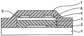
- FIG. 1 is a schematic cross-sectional view showing the structure of a bottom gate top contact type organic thin film transistor which is an embodiment of the present invention.
- the organic thin film transistor includes a substrate 1, a gate electrode 2 formed on the substrate 1, a gate insulating layer 3 formed on the gate electrode 2, an organic semiconductor layer 4 formed on the gate insulating layer 3, A source electrode 5 and a drain electrode 6 formed on the organic semiconductor layer 4 with a channel portion interposed therebetween, and an overcoat 7 covering the entire element are provided.
- a bottom gate top contact type organic thin film transistor includes, for example, a gate electrode formed on a substrate, a gate insulating layer formed on the gate electrode, an organic semiconductor layer formed on the gate insulating layer, and a source electrode formed on the organic semiconductor layer.
- the drain electrode can be formed, and if necessary, an overcoat can be formed.
- FIG. 2 is a schematic cross-sectional view showing the structure of a bottom gate bottom contact type organic thin film transistor which is an embodiment of the present invention.
- a substrate 1 a gate electrode 2 formed on the substrate 1, a gate insulating layer 3 formed on the gate electrode 2, and a channel portion on the gate insulating layer 3 are formed.
- a bottom gate bottom contact type organic thin film transistor includes, for example, a gate electrode formed on a substrate, a gate insulating layer formed on the gate electrode, a source electrode and a drain electrode formed on the gate insulating layer, and a source electrode and a drain electrode. It can be manufactured by forming an organic semiconductor layer on top and, if necessary, forming an overcoat.
- the gate insulating layer is formed by further adding a solvent or the like to the gate insulating resin composition to prepare an insulating layer coating solution, and applying, drying, and curing the insulating layer coating solution on the gate electrode.
- the organic solvent used in the insulating layer coating solution is not particularly limited as long as it dissolves the polymer compound and the crosslinking agent, but is preferably an organic solvent having a boiling point of 100 ° C. to 200 ° C. at normal pressure. is there. Examples of the organic solvent include 2-heptanone and propylene glycol monomethyl ether acetate.
- a leveling agent, a surfactant, a curing catalyst, and the like can be added to the insulating layer coating solution as necessary.
- the insulating layer coating solution can be applied onto the gate electrode by known spin coating, die coater, screen printing, ink jet or the like.
- Drying performed in the process of forming the gate insulating layer means removing the solvent of the applied resin composition.
- Curing means that the resin composition is crosslinked.
- the process of cross-linking the resin composition of the present invention includes, as a first step, a step in which the first functional group in the polymer compound (A) is deblocked to generate a second functional group that reacts with active hydrogen,
- the second step includes a step in which the generated second functional group reacts with the active hydrogen compound (B). Comparing the first stage and the second stage for crosslinking, the first stage has a slower reaction rate than the second stage, and therefore, once the first stage proceeds, the second stage proceeds automatically. Therefore, in order to cure the resin composition, the first stage for crosslinking may be advanced.
- Irradiation of electromagnetic waves can be performed using, for example, an exposure apparatus used for manufacturing a semiconductor or a UV lamp used for curing a UV curable resin. Calcination can be performed by heating at a relatively high temperature, for example, 80 to 300 ° C., preferably 120 to 250 ° C., for 5 minutes to 2 hours, preferably 10 minutes to 1 hour. Irradiation conditions and baking conditions for deblocking the first functional group contained in the polymer compound (A) are appropriately determined according to the type and amount of the first functional group.
- the contact angle of the gate insulating layer with respect to pure water is appropriately adjusted by increasing or decreasing the hydrophilicity of the surface in consideration of the amount of fluorine, hydrophobic functional group and hydrophilic functional group contained in the resin used for forming the layer. .
- the surface hydrophilicity of the gate insulating layer can be increased or decreased by heating in various gas atmospheres. For example, if the heating or baking (drying and curing, etc.) performed when forming the gate insulating layer is performed in an atmosphere containing oxygen, the surface hydrophilicity is increased, and if performed in an inert gas atmosphere, the surface hydrophilicity is decreased. To do. When heating is performed in an atmosphere containing oxygen, the surface hydrophilicity increases as the temperature is increased.
- a self-assembled monolayer may be formed on the gate insulating layer.
- the self-assembled monolayer can be formed, for example, by treating the gate insulating layer with a solution obtained by dissolving 1 to 10% by weight of an alkylchlorosilane compound or an alkylalkoxysilane compound in an organic solvent.
- alkylchlorosilane compound examples include methyltrichlorosilane, ethyltrichlorosilane, butyltrichlorosilane, decyltrichlorosilane, octadecyltrichlorosilane, and the like.
- alkylalkoxysilane compound examples include methyltrimethoxysilane, ethyltrimethoxysilane, butyltrimethoxysilane, decyltrimethoxysilane, octadecyltrimethoxysilane and the like.
- the substrate 1, gate electrode 2, source electrode 5, drain electrode 6 and organic semiconductor layer 4 may be composed of commonly used materials and methods.
- a resin or plastic plate or film, a glass plate, a silicon plate, or the like is used as the substrate material.
- As the material of the electrode chromium, gold, silver, aluminum or the like is used, and it is formed by a known method such as a vapor deposition method, a sputtering method, a printing method, or an ink jet method.
- organic semiconductor compounds As organic semiconductor compounds, ⁇ -conjugated polymers are widely used. For example, polypyrroles, polythiophenes, polyanilines, polyallylamines, fluorenes, polycarbazoles, polyindoles, poly (p-phenylene vinylene) s, etc. are used. be able to.
- low-molecular substances having solubility in organic solvents for example, polycyclic aromatic derivatives such as pentacene, phthalocyanine derivatives, perylene derivatives, tetrathiafulvalene derivatives, tetracyanoquinodimethane derivatives, fullerenes, carbon nanotubes Etc. can be used. Specific examples include condensates of 9,9-di-n-octylfluorene-2,7-di (ethylene boronate) and 5,5′-dibromo-2,2′-bithiophene. .
- the formation of the organic semiconductor layer is performed, for example, by adding a solvent or the like to the organic semiconductor compound to prepare an organic semiconductor coating solution, and applying and drying this on the gate insulating layer.
- the resin constituting the gate insulating layer has a phenyl moiety or a carbonyl moiety and has an affinity for an organic semiconductor compound. Therefore, a uniform and flat interface is formed between the organic semiconductor layer and the gate insulating layer by the coating and drying method.
- the solvent used is not particularly limited as long as it dissolves or disperses the organic semiconductor, but preferably has a boiling point of 50 ° C. to 200 ° C. at normal pressure.
- the solvent include chloroform, toluene, anisole, 2-heptanone, propylene glycol monomethyl ether acetate and the like.
- the organic semiconductor coating liquid can be applied onto the gate insulating layer by a known spin coating, die coater, screen printing, ink jet, or the like, similarly to the insulating layer coating liquid.
- the organic thin film transistor of the present invention may be coated with an overcoat material for the purpose of protecting the organic thin film transistor and improving the smoothness of the surface.
- the display member which has an organic thin-film transistor suitably can be produced using the organic thin-film transistor of the present invention.
- a display member having the organic thin film transistor a display including the display member can be suitably produced.
- Synthesis example 1 Styrene (made by Wako Pure Chemical Industries) 2.06 g, 2,3,4,5,6-pentafluorostyrene (made by Aldrich) 2.43 g, 2- [O- [1′-methylpropylideneamino] carboxyamino] ethyl -Methacrylate (made by Showa Denko, trade name “Karenz MOI-BM”) 1.00 g, 2,2′-azobis (2-methylpropionitrile) 0.06 g, 2-heptanone (made by Wako Pure Chemical Industries) 14.06 g Is put in a 50 ml pressure vessel (Ace), bubbled with nitrogen, sealed, and polymerized in an oil bath at 60 ° C. for 48 hours to give a viscous 2-heptanone solution in which the polymer compound 1 is dissolved. Got.
- the chemical structure of the polymer compound 1 is as follows.
- Synthesis example 2 Vinyl benzoate (manufactured by Aldrich) 22.22 g, 2,3,4,5,6-pentafluorostyrene (manufactured by Aldrich) 14.56 g, 2- [O- [1′-methylpropylideneamino] carboxyamino] ethyl- Methacrylate (made by Showa Denko, trade name “Karenz MOI-BM”) 6.00 g, 2,2′-azobis (2-methylpropionitrile) 0.43 g, 2-heptanone (made by Wako Pure Chemical Industries) 64.17 g , Put in a 125 ml pressure vessel (made by Ace), bubble nitrogen, seal tightly and polymerize in an oil bath at 60 ° C. for 48 hours to obtain a viscous 2-heptanone solution in which the polymer compound 2 is dissolved. Obtained.
- the chemical structure of the polymer compound 2 is as follows.
- Synthesis example 3 Mixture of 9,9-di-n-octylfluorene-2,7-di (ethylene boronate) 6.40 g, 5,5′-dibromo-2,2′-bithiophene 4.00 g in toluene (80 mL) Under nitrogen, 0.18 g of tetrakis (triphenylphosphine) palladium, 1.0 g of methyltrioctylammonium chloride (manufactured by Aldrich, trade name “Aliquat 336” (registered trademark)), and 24 mL of 2M aqueous sodium carbonate solution were added. . The mixture was stirred vigorously and heated at reflux for 24 hours.
- the viscous reaction mixture was poured into 500 mL of acetone to precipitate a fibrous yellow polymer.
- the polymer was collected by filtration, washed with acetone and dried in a vacuum oven at 60 ° C. overnight.
- the resulting polymer is referred to as polymer compound 3.
- the chemical structure of the polymer compound 3 is as follows.
- n is an integer.
- Synthesis example 4 4-aminostyrene (manufactured by Aldrich) 3.50 g, 2,3,4,5,6-pentafluorostyrene (manufactured by Aldrich) 13.32 g, 2,2′-azobis (2-methylpropionitrile) 0.08 g 25-36 g of 2-heptanone (manufactured by Wako Pure Chemical Industries, Ltd.) was placed in a 125 ml pressure vessel (manufactured by Ace), bubbled with nitrogen, sealed, and polymerized in an oil bath at 60 ° C. for 48 hours to obtain a polymer compound. A viscous 2-heptanone solution in which 4 was dissolved was obtained.
- the chemical structure of the polymer compound 4 is as follows.
- Synthesis example 5 2,3,4,5,6-pentafluorostyrene (manufactured by Aldrich) 28.31 g, 2- [O- [1′-methylpropylideneamino] carboxyamino] ethyl-methacrylate (manufactured by Showa Denko, trade name “Karenz MOI-BM ”) 15.00 g, 2,2′-azobis (2-methylpropionitrile) 0.43 g, 2-heptanone (manufactured by Wako Pure Chemical Industries) 65.61 g are placed in a 125 ml pressure vessel (manufactured by ACE). After bubbling nitrogen, the bottle was sealed and polymerized in an oil bath at 60 ° C. for 48 hours to obtain a viscous 2-heptanone solution in which the polymer compound 5 was dissolved.
- the chemical structure of the polymer compound 5 is as follows.
- Synthesis example 7 2.17 g of styrene (manufactured by Aldrich), 2.80 g of 2-trifluoroethyl methacrylate (manufactured by Aldrich), 2- [O- [1′-methylpropylideneamino] carboxyamino] ethyl-methacrylate (manufactured by Showa Denko, trade name) “Karenz MOI-BM”) 1.00 g, 2,2′-azobis (2-methylpropionitrile) 0.06 g, 2-heptanone (Wako Pure Chemical Industries, Ltd.) 11.77 g, 50 ml pressure vessel (Ace) The solution was bubbled with nitrogen, sealed, and polymerized in an oil bath at 60 ° C. for 48 hours to obtain a viscous 2-heptanone solution in which the polymer compound 7 was dissolved.
- the chemical structure of the polymer compound 7 is as follows.
- Synthesis example 8 1.66 g of styrene (manufactured by Wako Pure Chemical Industries), 3.87 g of 2,3,4,5,6-pentafluorostyrene (manufactured by Aldrich), 2- [N- [1 ′, 3′-dimethylpyrazolyl] carboxyamino] 8.
- ion exchange resin (Diaion RCP160M, manufactured by Mitsubishi Chemical Corporation) into a 50 ml beaker, wash with 20 ml of absolute ethanol, and filter three times, and then wash and filter with 50 ml of 2-heptanone.
- An ion exchange resin which was solvent-substituted with 2-heptanone was obtained.
- the ion-exchange resin solvent-substituted with 2-heptanone and a stirrer were placed in a 125 ml pressure vessel containing a viscous 2-heptanone solution and stirred with a magnetic stirrer at room temperature for 5 hours. After leaving stirring, the mixture was allowed to stand for a while, and then the viscous 2-heptanone solution was filtered off and dropped into 1000 ml of hexane to reprecipitate the polymer. The obtained polymer was filtered and dried to obtain polymer compound 12 as a white powder. The yield was 25 g.
- the chemical structure of the polymer compound 12 is as follows.
- Synthesis Example 15 18.52 g of vinyl benzoate (manufactured by Aldrich), 14.56 g of 2,3,4,5,6-pentafluorostyrene (manufactured by Aldrich), 2- [O- [1′-methylpropylideneamino] carboxyamino] ethyl- 12.00 g of methacrylate (made by Showa Denko, trade name “Karenz MOI-BM”), 0.45 g of 2,2′-azobis (2-methylpropionitrile), 67.62 g of 2-heptanone (manufactured by Wako Pure Chemical Industries) In a 125 ml pressure vessel (made by Ace), bubbling nitrogen, sealed, and polymerized in an oil bath at 60 ° C. for 48 hours to obtain a viscous 2-heptanone solution in which the polymer compound 15 was dissolved Obtained.
- the chemical structure of the polymer compound 15 is as follows.
- Example 1 3.00 g of a 2-heptanone solution of polymer compound 1 obtained in Synthesis Example 1,
- the obtained coating solution is filtered using a membrane filter having a pore size of 0.2 ⁇ m, spin-coated on a glass substrate with a chromium electrode, and then baked on a hot plate at 220 ° C. for 30 minutes to obtain a gate insulating layer. It was.
- the polymer compound 3 was dissolved in chloroform as a solvent to prepare a solution (organic semiconductor composition) having a concentration of 0.5% by weight, and this was filtered through a membrane filter to prepare a coating solution. .
- the obtained coating solution is applied on the gate insulating layer by a spin coating method to form an active layer having a thickness of about 60 nm, and then, on the active layer by a vacuum deposition method using a metal mask,
- a field effect organic thin film transistor was manufactured by forming a source electrode and a drain electrode (having a laminated structure in the order of fullerene and gold from the active layer side) having a channel length of 20 ⁇ m and a channel width of 2 mm.
- Example 2 3.00 g of a 2-heptanone solution of polymer compound 2 obtained in Synthesis Example 2,
- the obtained coating solution is filtered using a membrane filter having a pore size of 0.2 ⁇ m, spin-coated on a glass substrate with a chromium electrode, and then baked on a hot plate at 150 ° C. for 30 minutes to obtain a gate insulating layer. It was.
- Example 3 A field effect organic thin film transistor was produced in the same manner as in Example 2 except that the gate insulating layer was baked on a hot plate at 200 ° C. for 30 minutes.
- Example 4 A field effect organic thin film transistor was produced in the same manner as in Example 2 except that the gate insulating layer was baked on a hot plate at 220 ° C. for 30 minutes.
- Example 5 A field effect organic thin film transistor was fabricated in the same manner as in Example 2, except that the gate insulating layer was baked on a hot plate at 220 ° C. for 30 minutes in a nitrogen atmosphere.
- Example 6 A field effect organic thin film transistor was produced in the same manner as in Example 1 except that 0.034 g of p-phenylenediamine was used instead of 1,4-dihydroxybenzene.
- Example 7 2.00 g of the 2-heptanone solution of the polymer compound 1 obtained in Synthesis Example 1, 0.79 g of the 2-heptanone solution of the polymer compound 4 obtained in Synthesis Example 4 and 2.00 g of 2-heptanone were placed in a 10 ml sample bottle. The mixture was stirred and dissolved to prepare a uniform coating solution.
- the obtained coating solution is filtered using a membrane filter having a pore size of 0.2 ⁇ m, spin-coated on a glass substrate with a chromium electrode, and then baked on a hot plate at 220 ° C. for 30 minutes to obtain a gate insulating layer. It was.
- Example 8 1.00 g of the 2-heptanone solution of the polymer compound 5 obtained in Synthesis Example 5, 0.83 g of the 2-heptanone solution of the polymer compound 4 obtained in Synthesis Example 4 and 2.00 g of 2-heptanone were placed in a 10 ml sample bottle. The mixture was stirred and dissolved to prepare a uniform coating solution.
- the obtained coating solution is filtered using a membrane filter having a pore size of 0.2 ⁇ m, spin-coated on a glass substrate with a chromium electrode, and then baked on a hot plate at 220 ° C. for 30 minutes to obtain a gate insulating layer. It was.
- Example 9 2.00 g of 2-heptanone solution of polymer compound 6 obtained in Synthesis Example 6, 0.61 g of 2-heptanone solution of polymer compound 4 obtained in Synthesis Example 4 and 2.50 g of 2-heptanone were placed in a 10 ml sample bottle. The mixture was stirred and dissolved to prepare a uniform coating solution.
- the obtained coating solution was filtered using a membrane filter having a pore size of 0.2 ⁇ m, spin-coated on a glass substrate with a chromium electrode, and then heated on a hot plate at 100 ° C. for 10 minutes, 150 ° C. for 10 minutes, 220 Baking at 30 ° C. for 30 minutes gave a gate insulating layer.
- Example 10 2.00 g of the 2-heptanone solution of the polymer compound 7 obtained in Synthesis Example 7, 0.60 g of the 2-heptanone solution of the polymer compound 4 obtained in Synthesis Example 4 and 1.50 g of 2-heptanone were placed in a 10 ml sample bottle. The mixture was stirred and dissolved to prepare a uniform coating solution.
- the obtained coating solution was filtered using a membrane filter having a pore size of 0.2 ⁇ m, spin-coated on a glass substrate with a chromium electrode, and then heated on a hot plate at 100 ° C. for 10 minutes, 150 ° C. for 10 minutes, 220 Baking at 30 ° C. for 30 minutes gave a gate insulating layer.
- Example 11 2.00 g of 2-heptanone solution of polymer compound 8 obtained in Synthesis Example 8, 0.70 g of 2-heptanone solution of polymer compound 4 obtained in Synthesis Example 4 and 2.50 g of 2-heptanone were placed in a 10 ml sample bottle. The mixture was stirred and dissolved to prepare a uniform coating solution.
- the obtained coating solution was filtered using a membrane filter having a pore size of 0.2 ⁇ m, spin-coated on a glass substrate with a chromium electrode, and then heated on a hot plate at 100 ° C. for 10 minutes, 150 ° C. for 10 minutes, 220 Baking at 30 ° C. for 30 minutes gave a gate insulating layer.
- Example 12 In a 10 ml sample bottle, 3.00 g of a 2-heptanone solution of the polymer compound 9 obtained in Synthesis Example 9 and 0.036 g of 1,4-dihydroxybenzene and 1.50 g of 2-heptanone were stirred and dissolved to uniformly apply. A solution was prepared.
- the obtained coating solution is filtered using a membrane filter having a pore size of 0.2 ⁇ m, spin-coated on a glass substrate with a chromium electrode, and then baked on a hot plate at 200 ° C. for 30 minutes to obtain a gate insulating layer. It was.
- Example 13 6.00 g of a 2-heptanone solution of polymer compound 10 obtained in Synthesis Example 10, 0.072 g of 1,4-dihydroxybenzene, and 3.00 g of 2-heptanone were placed in a 10 ml sample bottle, dissolved by stirring and evenly coated. A solution was prepared.
- the obtained coating solution is filtered using a membrane filter having a pore size of 0.2 ⁇ m, spin-coated on a glass substrate with a chromium electrode, and then baked on a hot plate at 200 ° C. for 30 minutes to obtain a gate insulating layer. It was.
- Example 14 6.00 g of 2-heptanone solution of polymer compound 11 obtained in Synthesis Example 11, 0.072 g of 1,4-dihydroxybenzene, and 3.00 g of 2-heptanone were placed in a 10 ml sample bottle, and dissolved by stirring until uniform coating. A solution was prepared.
- the obtained coating solution is filtered using a membrane filter having a pore size of 0.2 ⁇ m, spin-coated on a glass substrate with a chromium electrode, and then baked on a hot plate at 200 ° C. for 30 minutes to obtain a gate insulating layer. It was.
- Example 15 3.00 g of a 2-heptanone solution of the polymer compound 1 obtained in Synthesis Example 1 and 42.4% by weight of BOPH resin (poly ⁇ dimethyl-2- (4′-hydroxyphenyl) ethylsilylsilsesquioxane ⁇ ) 2- 0.425 g of heptanone solution (manufactured by Toagosei Co., Ltd.) and 1.30 g of 2-heptanone were placed in a 10 ml sample bottle and dissolved by stirring to prepare a uniform coating solution.
- BOPH resin poly ⁇ dimethyl-2- (4′-hydroxyphenyl) ethylsilylsilsesquioxane ⁇
- 2- heptanone solution manufactured by Toagosei Co., Ltd.
- the obtained coating solution is filtered using a membrane filter having a pore size of 0.2 ⁇ m, spin-coated on a glass substrate with a chromium electrode, and then baked on a hot plate at 200 ° C. for 30 minutes to obtain a gate insulating layer. It was.
- Example 16 Place 3.00 g of the 2-heptanone solution of Polymer Compound 1 obtained in Synthesis Example 1 and 0.195 g of the powder of Polymer Compound 12 obtained in Synthesis Example 12 and 1.50 g of 2-heptanone into a 10 ml sample bottle and stir A uniform coating solution was prepared by dissolution.
- the obtained coating solution is filtered using a membrane filter having a pore size of 0.2 ⁇ m, spin-coated on a glass substrate with a chromium electrode, and then baked on a hot plate at 200 ° C. for 30 minutes to obtain a gate insulating layer. It was.
- Example 17 In a 10 ml sample bottle, 3.00 g of a 2-heptanone solution of polymer compound 13 obtained in Synthesis Example 13 and 0.037 g of 1,4-dihydroxybenzene and 1.50 g of 2-heptanone were stirred and dissolved to be uniformly coated. A solution was prepared.
- the obtained coating solution is filtered using a membrane filter having a pore size of 0.2 ⁇ m, spin-coated on a glass substrate with a chromium electrode, and then baked on a hot plate at 200 ° C. for 30 minutes to obtain a gate insulating layer. It was.
- Example 18 In a 10 ml sample bottle, 3.00 g of a 2-heptanone solution of polymer compound 14 obtained in Synthesis Example 14 and 0.029 g of 1,4-dihydroxybenzene and 1.50 g of 2-heptanone were stirred and dissolved, and uniformly coated. A solution was prepared.
- the obtained coating solution is filtered using a membrane filter having a pore size of 0.2 ⁇ m, spin-coated on a glass substrate with a chromium electrode, and then baked on a hot plate at 200 ° C. for 30 minutes to obtain a gate insulating layer. It was.
- Example 19 3.00 g of a 2-heptanone solution of polymer compound 1 obtained in Synthesis Example 1,
- the obtained coating solution is filtered using a membrane filter having a pore size of 0.2 ⁇ m, spin-coated on a glass substrate with a chromium electrode, and then baked on a hot plate at 200 ° C. for 30 minutes to obtain a gate insulating layer. It was.
- Example 20 3.00 g of a 2-heptanone solution of polymer compound 1 obtained in Synthesis Example 1,
- the obtained coating solution is filtered using a membrane filter having a pore size of 0.2 ⁇ m, spin-coated on a glass substrate with a chromium electrode, and then baked on a hot plate at 200 ° C. for 30 minutes to obtain a gate insulating layer. It was.
- Example 21 3.00 g of a 2-heptanone solution of polymer compound 1 obtained in Synthesis Example 1,
- the obtained coating solution is filtered using a membrane filter having a pore size of 0.2 ⁇ m, spin-coated on a glass substrate with a chromium electrode, and then baked on a hot plate at 150 ° C. for 30 minutes to obtain a gate insulating layer. It was.
- Example 22 2.00 g of 2-heptanone solution of polymer compound 2 obtained in Synthesis Example 2, 1.86 g of 2-heptanone solution of polymer compound 14 obtained in Synthesis Example 14 and 1.30 g of 2-heptanone were placed in a 10 ml sample bottle. The mixture was stirred and dissolved to prepare a uniform coating solution.
- the obtained coating solution is filtered using a membrane filter having a pore size of 0.2 ⁇ m, spin-coated on a glass substrate with a chromium electrode, and then baked on a hot plate at 220 ° C. for 30 minutes to obtain a gate insulating layer. It was.
- Example 23 A 2.00 g 2-heptanone solution of the polymer compound 15 obtained in Synthesis Example 15, 3.53 g of the 2-heptanone solution of the polymer compound 14 obtained in Synthesis Example 14 and 1.80 g of 2-heptanone were placed in a 10 ml sample bottle. The mixture was stirred and dissolved to prepare a uniform coating solution.
- the obtained coating solution is filtered using a membrane filter having a pore size of 0.2 ⁇ m, spin-coated on a glass substrate with a chromium electrode, and then baked on a hot plate at 220 ° C. for 30 minutes to obtain a gate insulating layer. It was.
- Example 24 2.00 g of the 2-heptanone solution of the polymer compound 15 obtained in Synthesis Example 15 and 4.53 g of the 2-heptanone solution of the polymer compound 16 obtained in Synthesis Example 16 were placed in a 10 ml sample bottle, and dissolved by stirring until uniform. A coating solution was prepared.
- the obtained coating solution is filtered using a membrane filter having a pore size of 0.2 ⁇ m, spin-coated on a glass substrate with a chromium electrode, and then baked on a hot plate at 220 ° C. for 30 minutes to obtain a gate insulating layer. It was.
- Example 25 2.00 g of a 2-heptanone solution of polymer compound 1 obtained in Synthesis Example 1,
- the obtained coating solution is filtered using a membrane filter having a pore size of 0.2 ⁇ m, spin-coated on a glass substrate with a chromium electrode, and then baked on a hot plate at 220 ° C. for 30 minutes to obtain a gate insulating layer. It was.
- Example 26 2.00 g of a 2-heptanone solution of polymer compound 1 obtained in Synthesis Example 1,
- the obtained coating solution is filtered using a membrane filter having a pore size of 0.2 ⁇ m, spin-coated on a glass substrate with a chromium electrode, and then baked on a hot plate at 220 ° C. for 30 minutes to obtain a gate insulating layer. It was.
- Example 27 2.00 g of a 2-heptanone solution of the polymer compound 1 obtained in Synthesis Example 1,
- the obtained coating solution is filtered using a membrane filter having a pore size of 0.2 ⁇ m, spin-coated on a glass substrate with a chromium electrode, and then baked on a hot plate at 220 ° C. for 30 minutes to obtain a gate insulating layer. It was.
- the field-effect organic thin film transistor thus fabricated has the transistor characteristics of a vacuum probe (BCT22MDC-5-5) under the condition that the gate voltage Vg is changed to 0 to ⁇ 60 V and the source-drain voltage Vsd is changed to 0 to ⁇ 60 V.
- Table 1 shows the results of measurement using HT-SCU (manufactured by Nagase Electronic Equipments Service Co., LTD).
- the hysteresis of the organic thin film transistor is that the threshold voltage Vth1 when the source-drain voltage Vsd is -40V and the gate voltage Vg is changed from 0V to -60V and the threshold voltage when the gate voltage Vg is changed from -60V to 0V. It was expressed as a voltage difference from the voltage Vth2.
- the ON / OFF ratio of the organic thin film transistor was obtained by dividing the current value when the gate voltage was 40 V by the current value at the start of the organic thin film transistor.
- a field effect organic thin film transistor was prepared in the same manner as in Example 1 except that this coating solution was used for forming the gate insulating layer, and transistor characteristics were measured and evaluated.
Landscapes
- Chemical & Material Sciences (AREA)
- Health & Medical Sciences (AREA)
- Chemical Kinetics & Catalysis (AREA)
- Medicinal Chemistry (AREA)
- Polymers & Plastics (AREA)
- Organic Chemistry (AREA)
- Emergency Medicine (AREA)
- Thin Film Transistor (AREA)
- Addition Polymer Or Copolymer, Post-Treatments, Or Chemical Modifications (AREA)
- Other Resins Obtained By Reactions Not Involving Carbon-To-Carbon Unsaturated Bonds (AREA)
- Polyurethanes Or Polyureas (AREA)
- Devices For Indicating Variable Information By Combining Individual Elements (AREA)
Abstract
Priority Applications (3)
| Application Number | Priority Date | Filing Date | Title |
|---|---|---|---|
| CN2009801338417A CN102138218B (zh) | 2008-08-28 | 2009-08-25 | 树脂组合物、栅极绝缘层和有机薄膜晶体管 |
| US13/060,456 US8476621B2 (en) | 2008-08-28 | 2009-08-25 | Resin composition, gate insulating layer, and organic thin film transistor |
| EP09809889.0A EP2320467B1 (fr) | 2008-08-28 | 2009-08-25 | Composition de résine, couche d'isolation de grille et transistor à couches minces organiques |
Applications Claiming Priority (6)
| Application Number | Priority Date | Filing Date | Title |
|---|---|---|---|
| JP2008219846 | 2008-08-28 | ||
| JP2008-219846 | 2008-08-28 | ||
| JP2009027625 | 2009-02-09 | ||
| JP2009168912 | 2009-07-17 | ||
| JP2009-168912 | 2009-07-17 | ||
| JP2009-027625 | 2009-11-27 |
Publications (1)
| Publication Number | Publication Date |
|---|---|
| WO2010024238A1 true WO2010024238A1 (fr) | 2010-03-04 |
Family
ID=41721406
Family Applications (1)
| Application Number | Title | Priority Date | Filing Date |
|---|---|---|---|
| PCT/JP2009/064768 WO2010024238A1 (fr) | 2008-08-28 | 2009-08-25 | Composition de résine, couche d’isolation de grille et transistor à couches minces organiques |
Country Status (7)
| Country | Link |
|---|---|
| US (1) | US8476621B2 (fr) |
| EP (1) | EP2320467B1 (fr) |
| JP (1) | JP5479817B2 (fr) |
| KR (1) | KR101572296B1 (fr) |
| CN (1) | CN102138218B (fr) |
| TW (1) | TWI488906B (fr) |
| WO (1) | WO2010024238A1 (fr) |
Cited By (17)
| Publication number | Priority date | Publication date | Assignee | Title |
|---|---|---|---|---|
| WO2010082525A1 (fr) * | 2009-01-14 | 2010-07-22 | 住友化学株式会社 | Composition de résine pour couche isolante |
| WO2011125690A1 (fr) * | 2010-04-01 | 2011-10-13 | 住友化学株式会社 | Composition contenant un solvant organique fluoré pour utilisation dans une couche isolante de transistor organique en couche mince |
| WO2011125691A1 (fr) * | 2010-04-01 | 2011-10-13 | 住友化学株式会社 | Composition de résine pour utilisation dans une couche isolante de transistor organique en couche mince, couche isolante de protection, et transistor organique en couche mince |
| US20110297920A1 (en) * | 2010-06-03 | 2011-12-08 | Sony Corporation | Thin film transistor,method of manufacturing the same, and electronic device |
| WO2011158929A1 (fr) * | 2010-06-17 | 2011-12-22 | 住友化学株式会社 | Matériau pour couche isolante réticulable par une énergie optique pour transistor organique en film mince, couche isolante d'enrobage et transistor organique en film mince |
| WO2012002436A1 (fr) * | 2010-06-30 | 2012-01-05 | 住友化学株式会社 | Matière de couche isolante pour un transistor organique en couche mince et transistor organique en couche mince |
| WO2012029700A1 (fr) * | 2010-08-30 | 2012-03-08 | 住友化学株式会社 | Composition pour couche isolante d'un transistor en couches minces organique, et transistor en couches minces organique |
| WO2012063845A1 (fr) * | 2010-11-10 | 2012-05-18 | 住友化学株式会社 | Matériau pour élément organique |
| WO2012108326A1 (fr) * | 2011-02-07 | 2012-08-16 | 住友化学株式会社 | Matériau de couche d'isolation de transistor à couche mince organique réticulable par l'énergie lumineuse et thermique |
| WO2012108327A1 (fr) * | 2011-02-07 | 2012-08-16 | 住友化学株式会社 | Matériau de couche d'isolation de transistor à couche mince organique réticulable par l'énergie lumineuse et thermique |
| JP2012209528A (ja) * | 2011-03-15 | 2012-10-25 | Kaneka Corp | 有機tft用ゲート絶縁膜および該絶縁膜を有する有機tft素子 |
| WO2012161175A1 (fr) * | 2011-05-24 | 2012-11-29 | 住友化学株式会社 | Matériau de couche isolante de transistor en couches minces organiques |
| WO2014196482A1 (fr) * | 2013-06-07 | 2014-12-11 | 富士フイルム株式会社 | Composition permettant de former un film d'isolation de grille, transistor organique à couche mince, papier électronique et dispositif d'affichage |
| WO2015114966A1 (fr) * | 2014-01-31 | 2015-08-06 | 富士フイルム株式会社 | Composition de formation de film conducteur, film conducteur, transistor à film mince organique, papier électronique, dispositif d'affichage et carte de câblage |
| JPWO2015190294A1 (ja) * | 2014-06-09 | 2017-05-25 | 旭硝子株式会社 | 撥インク剤、ネガ型感光性樹脂組成物、隔壁および光学素子 |
| WO2017141932A1 (fr) * | 2016-02-18 | 2017-08-24 | 住友化学株式会社 | Composé polymère, composition, couche isolante et transistor à couches minces organiques |
| WO2018043371A1 (fr) * | 2016-09-02 | 2018-03-08 | 住友化学株式会社 | Composé polymère, film dans lequel le composé polymère est durci et dispositif électronique comprenant le film |
Families Citing this family (23)
| Publication number | Priority date | Publication date | Assignee | Title |
|---|---|---|---|---|
| TW201126606A (en) * | 2009-09-15 | 2011-08-01 | Sumitomo Chemical Co | Photocrosslinkable organic thin-film transistor insulation layer material |
| JP5740836B2 (ja) * | 2009-10-29 | 2015-07-01 | 住友化学株式会社 | 光電変換素子 |
| JP5666251B2 (ja) * | 2009-11-17 | 2015-02-12 | 住友化学株式会社 | 光及び熱エネルギー架橋性有機薄膜トランジスタ絶縁層材料 |
| JP5766467B2 (ja) * | 2011-03-02 | 2015-08-19 | 株式会社東芝 | 薄膜トランジスタ及びその製造方法、表示装置 |
| WO2012161106A1 (fr) * | 2011-05-26 | 2012-11-29 | 住友化学株式会社 | Matériau pour couche d'isolation d'un transistor organique à couches minces |
| JP2013065839A (ja) * | 2011-09-01 | 2013-04-11 | Sumitomo Chemical Co Ltd | 有機薄膜トランジスタ絶縁層材料 |
| JP2013125902A (ja) * | 2011-12-15 | 2013-06-24 | Sumitomo Chemical Co Ltd | 有機薄膜トランジスタ絶縁層材料及び有機薄膜トランジスタ |
| JP6025326B2 (ja) * | 2011-12-21 | 2016-11-16 | 住友化学株式会社 | 電子デバイス絶縁層材料、及び電子デバイス |
| JP2013149861A (ja) * | 2012-01-20 | 2013-08-01 | Sumitomo Chemical Co Ltd | 有機薄膜トランジスタ絶縁層材料 |
| JP6087898B2 (ja) | 2012-03-01 | 2017-03-01 | 住友化学株式会社 | 電子デバイス絶縁層及び電子デバイス絶縁層の製造方法 |
| JP5974588B2 (ja) * | 2012-03-30 | 2016-08-23 | 三菱化学株式会社 | 電界効果トランジスタ、表示用パネル及び重合体 |
| US8692238B2 (en) * | 2012-04-25 | 2014-04-08 | Eastman Kodak Company | Semiconductor devices and methods of preparation |
| WO2013187507A1 (fr) * | 2012-06-15 | 2013-12-19 | Dic株式会社 | Film d'isolation et transistor organique en film mince utilisant ledit film |
| CN103073675B (zh) * | 2012-12-19 | 2014-09-24 | 吉林大学 | 可热固化、高介电常数的绝缘层材料及用于制备有机薄膜晶体管栅绝缘层 |
| CA2945263A1 (fr) | 2014-04-09 | 2015-10-15 | Christopher Rudd | Utilisation d'inhibiteurs ou d'activateurs de gsk -3 qui modulent l'expression de pd -1 ou de t-bet pour moduler l'immunite due aux lymphocytes t |
| JP6405772B2 (ja) * | 2014-07-31 | 2018-10-17 | 住友化学株式会社 | 組成物およびそれを用いた有機薄膜トランジスタ |
| US9458353B1 (en) * | 2015-04-15 | 2016-10-04 | International Business Machines Corporation | Additives for orientation control of block copolymers |
| EP3346515A4 (fr) * | 2015-09-02 | 2018-10-17 | FUJIFILM Corporation | Transistor à film mince organique, procédé de fabrication de transistor à film mince organique, composition de semi-conducteur organique, film semi-conducteur organique, et procédé de fabrication de film semi-conducteur organique |
| WO2017038948A1 (fr) * | 2015-09-02 | 2017-03-09 | 富士フイルム株式会社 | Transistor à film mince organique, procédé de fabrication de transistor à film mince organique, composition de semi-conducteur organique, film semi-conducteur organique, et procédé de fabrication de film semi-conducteur organique |
| JP7306790B2 (ja) * | 2015-09-04 | 2023-07-11 | 三菱瓦斯化学株式会社 | 化合物の精製方法 |
| JP6004459B1 (ja) * | 2015-12-08 | 2016-10-05 | 国立大学法人 奈良先端科学技術大学院大学 | 薄膜トランジスタとその製造方法および前記薄膜トランジスタを有する半導体装置 |
| US11603317B2 (en) * | 2018-11-29 | 2023-03-14 | 4th Phase Water Technologies, LLC | Binder-free and fouling-resistant CNT thin film membrane |
| JP7468295B2 (ja) * | 2020-10-27 | 2024-04-16 | 信越化学工業株式会社 | ポジ型レジスト材料及びパターン形成方法 |
Citations (5)
| Publication number | Priority date | Publication date | Assignee | Title |
|---|---|---|---|---|
| JPH08231675A (ja) * | 1994-09-22 | 1996-09-10 | Semiconductor Energy Lab Co Ltd | 樹脂組成物およびそれを有する電子ディバイス |
| JP2005281530A (ja) * | 2004-03-30 | 2005-10-13 | Kuraray Co Ltd | 熱可塑性エラストマー組成物 |
| JP2006028497A (ja) * | 2004-06-21 | 2006-02-02 | Samsung Electronics Co Ltd | 有機絶縁膜組成物およびこれを用いた有機絶縁膜のパターン形成方法および有機薄膜トランジスタおよびこれを含む表示素子 |
| JP2007042852A (ja) * | 2005-08-03 | 2007-02-15 | Kansai Paint Co Ltd | トランジスタ及びその製造方法 |
| JP2007305950A (ja) | 2006-04-12 | 2007-11-22 | Toppan Printing Co Ltd | 絶縁塗料、これから形成された有機絶縁膜、その形成方法および有機トランジスタ |
Family Cites Families (10)
| Publication number | Priority date | Publication date | Assignee | Title |
|---|---|---|---|---|
| US5637156A (en) * | 1994-09-22 | 1997-06-10 | Semiconductor Energy Laboratory Co., Ltd. | Resin Composition and an electronic device using the same |
| US6479605B1 (en) | 2001-05-15 | 2002-11-12 | E. I. Du Pont De Nemours And Company | High-durability, low-yellowing repellent for textiles |
| TW200712775A (en) | 2005-08-26 | 2007-04-01 | Sumitomo Chemical Co | Photosensitive paste |
| KR20080078645A (ko) * | 2005-12-15 | 2008-08-27 | 아사히 가라스 가부시키가이샤 | 함불소 중합체, 네거티브형 감광성 조성물 및 격벽 |
| JP2007177041A (ja) | 2005-12-27 | 2007-07-12 | Showa Denko Kk | 熱硬化性重合体 |
| JP5194503B2 (ja) * | 2006-04-12 | 2013-05-08 | 住友ベークライト株式会社 | 樹脂膜の製造方法、樹脂膜及び半導体装置 |
| JP2008007559A (ja) | 2006-06-27 | 2008-01-17 | Jsr Corp | 無機粉体含有樹脂組成物、転写フィルムおよびフラットパネルディスプレイ部材の製造方法 |
| WO2009037820A1 (fr) | 2007-09-19 | 2009-03-26 | Daicel Chemical Industries, Ltd. | Composition de résine durcissable et produit durci |
| JP2010007030A (ja) | 2008-06-30 | 2010-01-14 | Sumitomo Chemical Co Ltd | 絶縁層用組成物 |
| JP5199752B2 (ja) | 2008-06-30 | 2013-05-15 | 住友化学株式会社 | 有機薄膜トランジスタ及びその製造方法、並びにこの有機トランジスタを用いたディスプレイ用部材及びディスプレイ |
-
2009
- 2009-08-25 EP EP09809889.0A patent/EP2320467B1/fr not_active Not-in-force
- 2009-08-25 WO PCT/JP2009/064768 patent/WO2010024238A1/fr active Application Filing
- 2009-08-25 JP JP2009194111A patent/JP5479817B2/ja active Active
- 2009-08-25 KR KR1020117004387A patent/KR101572296B1/ko active IP Right Grant
- 2009-08-25 CN CN2009801338417A patent/CN102138218B/zh not_active Expired - Fee Related
- 2009-08-25 US US13/060,456 patent/US8476621B2/en active Active
- 2009-08-26 TW TW098128635A patent/TWI488906B/zh not_active IP Right Cessation
Patent Citations (5)
| Publication number | Priority date | Publication date | Assignee | Title |
|---|---|---|---|---|
| JPH08231675A (ja) * | 1994-09-22 | 1996-09-10 | Semiconductor Energy Lab Co Ltd | 樹脂組成物およびそれを有する電子ディバイス |
| JP2005281530A (ja) * | 2004-03-30 | 2005-10-13 | Kuraray Co Ltd | 熱可塑性エラストマー組成物 |
| JP2006028497A (ja) * | 2004-06-21 | 2006-02-02 | Samsung Electronics Co Ltd | 有機絶縁膜組成物およびこれを用いた有機絶縁膜のパターン形成方法および有機薄膜トランジスタおよびこれを含む表示素子 |
| JP2007042852A (ja) * | 2005-08-03 | 2007-02-15 | Kansai Paint Co Ltd | トランジスタ及びその製造方法 |
| JP2007305950A (ja) | 2006-04-12 | 2007-11-22 | Toppan Printing Co Ltd | 絶縁塗料、これから形成された有機絶縁膜、その形成方法および有機トランジスタ |
Non-Patent Citations (3)
| Title |
|---|
| APPL. PHYS. LETT., vol. 89, 2006, pages 093507 |
| APPL. PHYS. LETT., vol. 92, 2008, pages 183306 |
| See also references of EP2320467A4 |
Cited By (28)
| Publication number | Priority date | Publication date | Assignee | Title |
|---|---|---|---|---|
| WO2010082525A1 (fr) * | 2009-01-14 | 2010-07-22 | 住友化学株式会社 | Composition de résine pour couche isolante |
| GB2480184A (en) * | 2009-01-14 | 2011-11-09 | Sumitomo Chemical Co | Resin compositions for insulating layer |
| WO2011125690A1 (fr) * | 2010-04-01 | 2011-10-13 | 住友化学株式会社 | Composition contenant un solvant organique fluoré pour utilisation dans une couche isolante de transistor organique en couche mince |
| WO2011125691A1 (fr) * | 2010-04-01 | 2011-10-13 | 住友化学株式会社 | Composition de résine pour utilisation dans une couche isolante de transistor organique en couche mince, couche isolante de protection, et transistor organique en couche mince |
| JP2011225854A (ja) * | 2010-04-01 | 2011-11-10 | Sumitomo Chemical Co Ltd | 有機薄膜トランジスタ絶縁層用樹脂組成物、オーバーコート絶縁層及び有機薄膜トランジスタ |
| US20110297920A1 (en) * | 2010-06-03 | 2011-12-08 | Sony Corporation | Thin film transistor,method of manufacturing the same, and electronic device |
| WO2011158929A1 (fr) * | 2010-06-17 | 2011-12-22 | 住友化学株式会社 | Matériau pour couche isolante réticulable par une énergie optique pour transistor organique en film mince, couche isolante d'enrobage et transistor organique en film mince |
| WO2012002436A1 (fr) * | 2010-06-30 | 2012-01-05 | 住友化学株式会社 | Matière de couche isolante pour un transistor organique en couche mince et transistor organique en couche mince |
| WO2012029700A1 (fr) * | 2010-08-30 | 2012-03-08 | 住友化学株式会社 | Composition pour couche isolante d'un transistor en couches minces organique, et transistor en couches minces organique |
| JP2012074683A (ja) * | 2010-08-30 | 2012-04-12 | Sumitomo Chemical Co Ltd | 有機薄膜トランジスタ絶縁層用組成物及び有機薄膜トランジスタ |
| WO2012063845A1 (fr) * | 2010-11-10 | 2012-05-18 | 住友化学株式会社 | Matériau pour élément organique |
| JP2012117058A (ja) * | 2010-11-10 | 2012-06-21 | Sumitomo Chemical Co Ltd | 有機素子材料 |
| WO2012108326A1 (fr) * | 2011-02-07 | 2012-08-16 | 住友化学株式会社 | Matériau de couche d'isolation de transistor à couche mince organique réticulable par l'énergie lumineuse et thermique |
| WO2012108327A1 (fr) * | 2011-02-07 | 2012-08-16 | 住友化学株式会社 | Matériau de couche d'isolation de transistor à couche mince organique réticulable par l'énergie lumineuse et thermique |
| JP2012209528A (ja) * | 2011-03-15 | 2012-10-25 | Kaneka Corp | 有機tft用ゲート絶縁膜および該絶縁膜を有する有機tft素子 |
| US9035292B2 (en) | 2011-05-24 | 2015-05-19 | Sumitomo Chemical Company, Limited | Organic thin-film transistor insulating layer material |
| JP2013102116A (ja) * | 2011-05-24 | 2013-05-23 | Sumitomo Chemical Co Ltd | 有機薄膜トランジスタ絶縁層材料 |
| WO2012161175A1 (fr) * | 2011-05-24 | 2012-11-29 | 住友化学株式会社 | Matériau de couche isolante de transistor en couches minces organiques |
| JPWO2014196482A1 (ja) * | 2013-06-07 | 2017-02-23 | 富士フイルム株式会社 | ゲート絶縁膜形成用組成物、有機薄膜トランジスタ、電子ペーパー、ディスプレイデバイス |
| WO2014196482A1 (fr) * | 2013-06-07 | 2014-12-11 | 富士フイルム株式会社 | Composition permettant de former un film d'isolation de grille, transistor organique à couche mince, papier électronique et dispositif d'affichage |
| US10014474B2 (en) | 2013-06-07 | 2018-07-03 | Fujifilm Corporation | Composition for forming gate insulating film, organic thin film transistor, electronic paper, and display device |
| WO2015114966A1 (fr) * | 2014-01-31 | 2015-08-06 | 富士フイルム株式会社 | Composition de formation de film conducteur, film conducteur, transistor à film mince organique, papier électronique, dispositif d'affichage et carte de câblage |
| JP6043000B2 (ja) * | 2014-01-31 | 2016-12-14 | 富士フイルム株式会社 | 導電膜形成用組成物、導電膜、有機薄膜トランジスタ、電子ペーパー、ディスプレイデバイスおよび配線板 |
| JPWO2015190294A1 (ja) * | 2014-06-09 | 2017-05-25 | 旭硝子株式会社 | 撥インク剤、ネガ型感光性樹脂組成物、隔壁および光学素子 |
| WO2017141932A1 (fr) * | 2016-02-18 | 2017-08-24 | 住友化学株式会社 | Composé polymère, composition, couche isolante et transistor à couches minces organiques |
| WO2018043371A1 (fr) * | 2016-09-02 | 2018-03-08 | 住友化学株式会社 | Composé polymère, film dans lequel le composé polymère est durci et dispositif électronique comprenant le film |
| JPWO2018043371A1 (ja) * | 2016-09-02 | 2018-09-13 | 住友化学株式会社 | 高分子化合物、該高分子化合物を硬化した膜及び該膜を含む電子デバイス |
| US10676554B2 (en) | 2016-09-02 | 2020-06-09 | Sumitomo Chemical Company, Limited | Polymer compound, film obtained by hardening this polymer compound and electronic device comprising this film |
Also Published As
| Publication number | Publication date |
|---|---|
| EP2320467B1 (fr) | 2014-08-13 |
| US8476621B2 (en) | 2013-07-02 |
| CN102138218B (zh) | 2013-07-31 |
| CN102138218A (zh) | 2011-07-27 |
| US20110193071A1 (en) | 2011-08-11 |
| JP2011038062A (ja) | 2011-02-24 |
| JP5479817B2 (ja) | 2014-04-23 |
| KR101572296B1 (ko) | 2015-11-26 |
| TW201020287A (en) | 2010-06-01 |
| EP2320467A4 (fr) | 2012-03-14 |
| TWI488906B (zh) | 2015-06-21 |
| EP2320467A1 (fr) | 2011-05-11 |
| KR20110055572A (ko) | 2011-05-25 |
Similar Documents
| Publication | Publication Date | Title |
|---|---|---|
| JP5479817B2 (ja) | 有機薄膜トランジスタゲート絶縁層用樹脂組成物、ゲート絶縁層及び有機薄膜トランジスタ | |
| JP6034056B2 (ja) | 有機薄膜トランジスタ絶縁層材料 | |
| JP5666251B2 (ja) | 光及び熱エネルギー架橋性有機薄膜トランジスタ絶縁層材料 | |
| WO2012161106A1 (fr) | Matériau pour couche d'isolation d'un transistor organique à couches minces | |
| JP5695467B2 (ja) | 有機薄膜トランジスタ絶縁層用樹脂組成物、オーバーコート絶縁層及び有機薄膜トランジスタ | |
| JPWO2017141932A1 (ja) | 高分子化合物、組成物、絶縁層および有機薄膜トランジスタ | |
| WO2011125690A1 (fr) | Composition contenant un solvant organique fluoré pour utilisation dans une couche isolante de transistor organique en couche mince | |
| JP6025326B2 (ja) | 電子デバイス絶縁層材料、及び電子デバイス | |
| JP5890633B2 (ja) | 有機薄膜トランジスタ絶縁層用組成物及び有機薄膜トランジスタ | |
| WO2012108327A1 (fr) | Matériau de couche d'isolation de transistor à couche mince organique réticulable par l'énergie lumineuse et thermique | |
| WO2012002436A1 (fr) | Matière de couche isolante pour un transistor organique en couche mince et transistor organique en couche mince | |
| JP6056443B2 (ja) | 絶縁層材料及び該絶縁層材料を用いて形成した有機薄膜トランジスタ | |
| WO2012108326A1 (fr) | Matériau de couche d'isolation de transistor à couche mince organique réticulable par l'énergie lumineuse et thermique | |
| JP5980522B2 (ja) | 有機薄膜トランジスタ絶縁層材料 | |
| WO2013031820A1 (fr) | Matériau de couche isolante pour transistor à couche mince organique | |
| JP2013258301A (ja) | 有機薄膜トランジスタ絶縁層材料 | |
| JP2010037462A (ja) | ゲート絶縁層用樹脂組成物 | |
| JP2013064095A (ja) | 有機薄膜トランジスタ絶縁層材料 |
Legal Events
| Date | Code | Title | Description |
|---|---|---|---|
| WWE | Wipo information: entry into national phase |
Ref document number: 200980133841.7 Country of ref document: CN |
|
| 121 | Ep: the epo has been informed by wipo that ep was designated in this application |
Ref document number: 09809889 Country of ref document: EP Kind code of ref document: A1 |
|
| ENP | Entry into the national phase |
Ref document number: 20117004387 Country of ref document: KR Kind code of ref document: A |
|
| WWE | Wipo information: entry into national phase |
Ref document number: 2009809889 Country of ref document: EP |
|
| NENP | Non-entry into the national phase |
Ref country code: DE |
|
| WWE | Wipo information: entry into national phase |
Ref document number: 13060456 Country of ref document: US |