US8995218B2 - Semiconductor device - Google Patents
Semiconductor device Download PDFInfo
- Publication number
- US8995218B2 US8995218B2 US13/783,573 US201313783573A US8995218B2 US 8995218 B2 US8995218 B2 US 8995218B2 US 201313783573 A US201313783573 A US 201313783573A US 8995218 B2 US8995218 B2 US 8995218B2
- Authority
- US
- United States
- Prior art keywords
- circuit
- power supply
- memory
- transistor
- arithmetic circuit
- Prior art date
- Legal status (The legal status is an assumption and is not a legal conclusion. Google has not performed a legal analysis and makes no representation as to the accuracy of the status listed.)
- Expired - Fee Related, expires
Links
Images


Classifications
-
- G—PHYSICS
- G11—INFORMATION STORAGE
- G11C—STATIC STORES
- G11C5/00—Details of stores covered by group G11C11/00
- G11C5/14—Power supply arrangements, e.g. power down, chip selection or deselection, layout of wirings or power grids, or multiple supply levels
-
- G—PHYSICS
- G11—INFORMATION STORAGE
- G11C—STATIC STORES
- G11C7/00—Arrangements for writing information into, or reading information out from, a digital store
-
- H—ELECTRICITY
- H10—SEMICONDUCTOR DEVICES; ELECTRIC SOLID-STATE DEVICES NOT OTHERWISE PROVIDED FOR
- H10D—INORGANIC ELECTRIC SEMICONDUCTOR DEVICES
- H10D30/00—Field-effect transistors [FET]
- H10D30/60—Insulated-gate field-effect transistors [IGFET]
- H10D30/67—Thin-film transistors [TFT]
-
- H—ELECTRICITY
- H10—SEMICONDUCTOR DEVICES; ELECTRIC SOLID-STATE DEVICES NOT OTHERWISE PROVIDED FOR
- H10D—INORGANIC ELECTRIC SEMICONDUCTOR DEVICES
- H10D86/00—Integrated devices formed in or on insulating or conducting substrates, e.g. formed in silicon-on-insulator [SOI] substrates or on stainless steel or glass substrates
- H10D86/201—Integrated devices formed in or on insulating or conducting substrates, e.g. formed in silicon-on-insulator [SOI] substrates or on stainless steel or glass substrates the substrates comprising an insulating layer on a semiconductor body, e.g. SOI
-
- G—PHYSICS
- G06—COMPUTING OR CALCULATING; COUNTING
- G06F—ELECTRIC DIGITAL DATA PROCESSING
- G06F1/00—Details not covered by groups G06F3/00 - G06F13/00 and G06F21/00
- G06F1/16—Constructional details or arrangements
- G06F1/20—Cooling means
- G06F1/206—Cooling means comprising thermal management
-
- G—PHYSICS
- G06—COMPUTING OR CALCULATING; COUNTING
- G06F—ELECTRIC DIGITAL DATA PROCESSING
- G06F1/00—Details not covered by groups G06F3/00 - G06F13/00 and G06F21/00
- G06F1/26—Power supply means, e.g. regulation thereof
- G06F1/32—Means for saving power
- G06F1/3203—Power management, i.e. event-based initiation of a power-saving mode
-
- G—PHYSICS
- G11—INFORMATION STORAGE
- G11C—STATIC STORES
- G11C5/00—Details of stores covered by group G11C11/00
- G11C5/14—Power supply arrangements, e.g. power down, chip selection or deselection, layout of wirings or power grids, or multiple supply levels
- G11C5/148—Details of power up or power down circuits, standby circuits or recovery circuits
Definitions
- the present invention relates to a semiconductor device.
- a semiconductor device in this specification refers to general devices which can function by utilizing semiconductor characteristics; for example, a semiconductor integrated circuit including a semiconductor element such as a transistor, an electro-optical device such as a display device, and an electronic device are all semiconductor devices.
- CPUs central processing units
- DSPs digital signal processors
- clock gating by which clocks are partly stopped As a method for reducing power consumption of the integrated circuit, clock gating by which clocks are partly stopped, a method for lowering the clock frequency, and a method for lowering power supply voltage partly have been developed.
- Power consumption includes static power due to leakage current of an element such as a transistor in the off state, as well as dynamic power due to charge and discharge caused by switching of the element.
- the static power can be almost negligible in integrated circuits with a small number of elements, but is too high to ignore in integrated circuits with an enormous number of elements.
- the following method power gating
- supply of a power supply voltage to circuits in the integrated circuit is controlled by switches (also referred to as power supply control switches or power gates).
- Patent Document 1 discloses a semiconductor integrated circuit that can implement power gating. Specifically, Patent Document 1 discloses a semiconductor integrated circuit that includes a transistor between a logic circuit and a power supply line, and can control supply of a power supply voltage to the logic circuit by controlling switching of the transistor.
- Patent Document 2 discloses a microcomputer or the like which can stop supply of a power supply voltage to a CPU, a memory, and the like in a period during which supplying power is not necessary, for example.
- an integrated circuit which includes a power supply control switch and be capable of power gating operates at a constant speed. Note that this operation is called normal operation for convenience (step S_ 10 ).
- step S_ 11 whether a period during which supply of power to the arithmetic circuit is stopped (power-off period) can be secured or not is determined. Since the power-off period can be secured while the arithmetic circuit is not operating (e.g., operation clock is not input), this determination depends on a relation between the operation speed of the arithmetic circuit and overhead at the time of writing or reading data to/from the nonvolatile memory.
- step S_ 12 data obtained by the arithmetic circuit is written to a nonvolatile memory. Note that in the case where the power-off period with respect to the arithmetic circuit is not secured, normal operation continues (step S_ 10 ).
- the power supply control switch provided between the arithmetic circuit and a power supply is turned off, whereby supply of power to the arithmetic circuit is stopped (step S_ 13 ).
- step S_ 14 After the power supply control switch is turned off, whether restoring of the written data is needed or not is determined (step S_ 14 ). This determination state lasts until the arithmetic circuit is made to operate again. In the case where the arithmetic circuit is not made to operate again and restoring of the data is not necessary, the power gate remains off (step S_ 13 ). Thus, power is not supplied to the arithmetic circuit until the arithmetic circuit is made to operate again.
- step S_ 15 the power supply control switch is turned on, so that the supply of power to the arithmetic circuit is restarted.
- step S_ 16 the transferred data is read from the nonvolatile memory and restored in the arithmetic circuit.
- step S_ 17 the normal operation is carried out again.
- overhead depends on electric characteristics of an element included in the nonvolatile memory. In other words, when the electric characteristics of the element changes with fluctuation of temperatures of a chip including a semiconductor integrated circuit, the amount of overhead also fluctuates.
- FIGS. 16A to 16C show relations between the power gating and overhead. Note that in each of FIGS. 16A to 16C , the horizontal axis indicates time, and the vertical axis indicates consumed power.
- FIG. 16A shows the case of Condition 1 where the condition indicates temperatures of a semiconductor memory device with nonvolatility (also referred to as nonvolatile memory) and a peripheral circuit controlling the nonvolatile memory;
- FIG. 16B shows the case of Condition 2;
- FIG. 16C shows the case of Condition 3.
- Condition 1 has the lowest temperatures of the nonvolatile memory and the peripheral circuit, which is followed by Condition 2 and Condition 3.
- Condition 3 has the lowest operation speeds of the nonvolatile memory and the peripheral circuit, which is followed by Condition 2 and Condition 1.
- regions represented as “a” and “b” mean overhead, and a region represented as “c” means power which can be reduced by power gating.
- a region represented as “c” means power which can be reduced by power gating.
- the relation a+b ⁇ c needs to be satisfied. The case where the above relation is not satisfied leads to an increase in power consumption.
- the amount of overhead under Condition 3 shown in FIG. 16C is largest; in that case, the relation a+b ⁇ c is satisfied, whereby power consumption of the semiconductor integrated circuit can be reduced.
- the relation a+b ⁇ c is satisfied under the condition where the electric characteristics of an element are poor, i.e., the amount of overhead is large, supply of power is stopped. Therefore, for example, in the case where high speed operation with a small amount of overhead is carried out, supply of power cannot be stopped even when there is a period during which supply of power can be stopped; accordingly, power is constantly supplied during high speed operation.
- An object of one embodiment of the present invention is to provide a semiconductor device with low power consumption.
- a plurality of temperature sensors are provided in a semiconductor device which is capable of power gating and includes a plurality of circuit blocks, temperatures of the circuit blocks are detected by the respective temperature sensors, and off periods appropriate to the temperatures are set in the respective circuit blocks. Specifically, the temperature of a memory circuit provided in each circuit block is detected, and an off period appropriate to the temperature is set in each circuit block.
- the circuit block indicates an assembly including circuits or memory mediums having a function such as arithmetic processing or data retention, in a semiconductor device.
- one embodiment of the present invention is a semiconductor device including an arithmetic circuit, a memory circuit configured to hold data obtained by the arithmetic circuit, a power supply control switch configured to control supply of a power supply voltage to the arithmetic circuit, a temperature detection circuit configured to detect a temperature of the memory circuit and to estimate an overhead from the temperature, and a controller configured to set a period during which the supply of the power supply voltage is stopped in the case where a power consumption of the arithmetic circuit during the period is larger than the overhead and to control the power supply control switch.
- overhead indicates extra power consumed at a time of writing and reading data to/from a memory circuit.
- Another embodiment of the present invention is a semiconductor device including an arithmetic circuit, a cache memory, a memory circuit configured to hold data obtained by the arithmetic circuit and data stored in the cache memory, a power supply control switch configured to control supply of a power supply voltage to the arithmetic circuit and the cache memory, a temperature detection circuit configured to detect a temperature of the memory circuit and to estimate an overhead from the temperature, and a controller configured to set a period during which the supply of the power supply voltage is stopped in the case where a power consumption of the arithmetic circuit and the cache memory during the period is larger than the overhead and to control the power supply control switch.
- the memory circuit is mainly constituted by semiconductor devices with nonvolatility (also referred to as nonvolatile memory), and examples of the nonvolatile memory include a flash memory including a transistor, a magnetoresistive random access memory using a magnetic tunnel junction (MTJ) element, a resistive random access memory (ReRAM), and a phase change random access memory (PRAM).
- a transistor with extremely low off-state current is employed for a transistor included in a volatile memory, whereby such a volatile memory can function as a nonvolatile memory and be applied to a nonvolatile memory in the memory circuit.
- the transistor with extremely low off-state current a transistor in which a channel formation region is formed using an oxide semiconductor (hereinafter, referred to as transistor including an oxide semiconductor) is given.
- the off-state current can be 100 zA or less per micrometer of the channel width by reducing oxygen vacancies and hydrogen in the oxide semiconductor.
- a switching element electrically connected to a wiring to which a power supply potential is supplied can be used.
- the switching element a transistor or the like is used.
- the power gate may have one transistor or a plurality of transistors. In a structure where a plurality of transistors are provided, the plurality of transistors may be connected to each other in parallel, in series, or in combination of a parallel connection and a series connection. Note that as the transistor included in the power gate, a transistor in which a channel formation region is formed using an oxide semiconductor can be used.
- temperature sensors are provided in circuit blocks in a semiconductor device, temperatures of the circuit blocks are detected by the respective temperature sensors, and an off period (period during which supply of power is stopped) appropriate to each circuit block can be set.
- an off period periodic during which supply of power is stopped
- a power-off period can be set, so that power consumption of the semiconductor device can be reduced.
- a semiconductor device can operate at high speed with cutting power consumption.
- FIG. 1 illustrates an example of a semiconductor device.
- FIG. 2 shows a power supply control switch of a semiconductor device.
- FIG. 3 shows a controller of a semiconductor device.
- FIGS. 4A and 4B each show a temperature sensor of a semiconductor device.
- FIG. 5 shows temperature characteristics of a diode included in a temperature sensor.
- FIG. 6 shows a semiconductor memory device included in a memory circuit of a semiconductor device.
- FIG. 7 shows a semiconductor memory device included in a memory circuit of a semiconductor device.
- FIGS. 8A and 8B show operation of a semiconductor memory device included in a memory circuit of a semiconductor device.
- FIG. 9 shows operation of a semiconductor device.
- FIGS. 10A to 10C each show a relation between overhead and a power-off period.
- FIGS. 11A to 11C each illustrate a structure of a transistor included in a semiconductor device.
- FIG. 12 shows electric characteristics of a transistor included in a semiconductor device.
- FIGS. 13A and 13B each illustrate an example of a semiconductor memory device included in a memory device in a semiconductor device.
- FIGS. 14A to 14F illustrate electronic devices.
- FIG. 15 shows an example of power gating.
- FIGS. 16A to 16C each show a period during which supply of power is stopped by the power gating described with FIG. 15 .
- FIG. 1 a structure example of a semiconductor device which is one embodiment of the present invention will be described with reference to FIG. 1 .
- a processor is described as an example of a semiconductor device which is one embodiment of the present invention.
- FIG. 1 is a block diagram of a processor 100 .
- the processor 100 includes an arithmetic circuit 105 and a cache memory 107 .
- the processor 100 includes a power supply control switch 101 functioning as a power gate between a power supply 119 and the arithmetic circuit 105 and a power supply control switch 103 functioning as a power gate between the power supply 119 and the cache memory 107 .
- the processor 100 includes a controller 117 which controls the power supply control switch 101 and the power supply control switch 103 .
- the processor 100 includes a memory circuit 109 which holds data obtained by the arithmetic circuit 105 and a memory circuit 111 which holds data stored in the cache memory 107 .
- the processor 100 includes a temperature detection circuit 113 which detects the temperature of the memory circuit 109 and estimates overhead from the temperature and a temperature detection circuit 115 which detects the temperature of the memory circuit 111 and estimates overhead from the temperature.
- a temperature detection circuit 113 which detects the temperature of the memory circuit 109 and estimates overhead from the temperature
- a temperature detection circuit 115 which detects the temperature of the memory circuit 111 and estimates overhead from the temperature.
- the arithmetic circuit 105 is preferably a logic circuit which is used generally and includes at least one of combination circuits such as an AND circuit, an OR circuit, a NAND circuit, and NOR circuit, for example. Note that the arithmetic circuit 105 may have a structure in which a sequential circuit such as a flip-flop is combined with the above combination circuit. Although not illustrated, the arithmetic circuit 105 includes a peripheral circuit which controls arithmetic processing.
- the cache memory 107 is preferably a cache memory which is generally used and formed with a combination of sequential circuits such as a flip-flow, and the like. Specifically, a cache memory including an SRAM can be used as the cache memory 107 . Although not illustrated, the cache memory 107 includes a peripheral circuit which controls operation of writing, reading, and the like.
- the memory circuit 109 and the memory circuit 111 each include a semiconductor memory device with nonvolatility (nonvolatile memory) and an operation circuit which drives the nonvolatile memory.
- the nonvolatile memory include a flash memory (including NAND type and NOR type), a magnetoresistive random access memory using a magnetic tunnel junction (MTJ) element, a resistive random access memory (ReRAM), and a phase change random access memory (PRAM).
- the operation circuit outputs a signal for transmitting data obtained by the arithmetic circuit 105 or data stored in the cache memory 107 to the memory circuit 109 or the memory circuit 111 before supply of the power supply voltage is stopped.
- a transistor with extremely low off-state current when used as a transistor included in a volatile memory, such a volatile memory can function as a nonvolatile memory and be applied to a nonvolatile memories included in the memory circuit 109 and the memory circuit 111 .
- the transistor with extremely low off-state current is, for example, a transistor including an oxide semiconductor, and the details of the transistor including an oxide semiconductor is described later.
- the arithmetic circuit 105 and the memory circuit 109 are independently provided in FIG. 1 , the arithmetic circuit 105 and the memory circuit 109 may be formed integrally, and the cache memory 107 and the memory circuit 111 may also be formed integrally.
- the temperature detection circuit 113 and the temperature detection circuit 115 each include a temperature sensor including a diode and a peripheral circuit controlling the temperature sensor.
- the temperature detection circuit 113 which detects the temperature of the memory circuit 109 and estimates overhead from the temperature
- the temperature detection circuit 115 which detects the temperature of the memory circuit 111 and estimates overhead from the temperature are provided independently.
- two temperature sensors may be provided in either one of the temperature detection circuits and switched by a switch to detect the temperatures of the memory circuit 109 and the memory circuit 111 , thereby deriving overhead from the temperatures.
- overhead which is estimated by the temperature detection circuit 113 and the temperature detection circuit 115 from the temperatures of the memory circuit 109 and the memory circuit 111 can be referred to as temperature data.
- a switching element electrically connected to a wiring to which the power supply potential is supplied can be used.
- the switching element include a transistor.
- the power supply control switch 101 has a function of controlling supply of the power supply voltage to the arithmetic circuit 105 .
- the power supply control switch 103 has a function of controlling supply of the power supply potential to the cache memory 107 .
- a transistor with extremely low off-state current may be used.
- Examples of the transistor with extremely low-off state current include a transistor including an oxide semiconductor (the details are described later).
- Each of the power supply control switch 101 and the power supply control switch 103 may have either one transistor or a plurality of transistors. Here, an example of providing a plurality of transistors is described.
- FIG. 2 is a circuit diagram of an example of a circuit configuration which can be applied to the power supply control switch 101 and the power supply control switch 103 .
- Each of the power supply control switch 101 and the power supply control switch 103 includes an n-channel transistor 121 and an n-channel transistor 122 .
- the transistor 121 is provided between the power supply 119 and the arithmetic circuit 105 or the cache memory 107 .
- a control signal SW_ON is input from the controller 117 . Whether or not the power supply voltage is supplied to the arithmetic circuit 105 or the cache memory 107 is controlled by turning on or off the transistor 121 .
- a control signal SW_OFF is input from the controller 117 . Whether or not the ground potential is supplied to the arithmetic circuit 105 or the cache memory 107 is controlled by turning on or off the transistor 122 .
- the power supply control switch in FIG. 2 is on when the transistor 121 is on and the transistor 122 is off.
- the power supply control switch in FIG. 2 is off when the transistor 121 is off and the transistor 122 is on.
- only one transistor is included in each of the power supply control switch 101 and the power supply control switch 103 , only one of the transistor 121 and the transistor 122 is provided in the power supply control switch shown in FIG. 2 .
- the power supply voltage is supplied while the gate of the transistor 121 is supplied with the control signal SW_ON, and supply of the power supply voltage is stopped while the gate of the transistor 121 is not supplied with the control signal SW_ON.
- the controller 117 is configured to receive the temperature data of the memory circuit 109 and the memory circuit 111 , which is calculated by the temperature detection circuit 113 and the temperature detection circuit 115 , and to output a signal for controlling switching (control signal SW_ON or control signal SW_OFF) of the power supply control switch 101 and the power supply control switch 103 in accordance with the temperature data. This is because overhead due to writing and reading processing of the nonvolatile memories included in the memory circuit 109 and the memory circuit 111 varies depending on the temperatures.
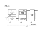
- FIG. 3 shows a configuration example of the controller 117 .
- the controller 117 includes an interface unit 151 , a clock generation unit 152 , an output signal control unit 153 , and a buffer unit 154 .
- the temperature data calculated by the temperature detection circuit 113 and the temperature detection circuit 115 and other input signals such as an instruction signal and input signal are input to the output signal control unit 153 through the interface unit 151 .
- the clock generation unit 152 generates a clock signal used in the controller 117 by using an inputted clock signal, and outputs the generated clock signal to the circuits (the output signal control unit 153 included).
- dividing the frequency of the inputted clock signal to be used in the controller 117 can reduce power consumption of the controller 117 .
- the output signal control unit 153 includes a counter circuit 155 .
- the output signal control unit 153 has a function of counting clock signals by the counter circuit 155 and setting the state (high/low) of a plurality of output signals in accordance with a signal (e.g., the temperature data calculated by the temperature detection circuit 113 and the temperature detection circuit 115 ) input to the controller 117 .
- Examples of the plurality of signals include a control signal for controlling the power supply control switch 101 and the power supply control switch 103 independently (e.g., control signal SW_ON or control signal SW_OFF).
- the control signal generated in the output signal control unit 153 is output to the power supply control switch 101 or the power supply control switch 103 through the buffer unit 154 .
- the processor 100 in FIG. 1 includes one arithmetic circuit and one cache memory as the arithmetic circuit 105 and the cache memory 107 , the structure is not limited thereto. Two or more arithmetic circuits 105 and two or more cache memories 107 may be provided. Moreover, a circuit block having another function may be additionally provided. In that case, the number of power supply control switches, the number of memory circuits, and the number of temperature detection circuits are determined in accordance with the number of the provided arithmetic circuits 105 , the number of the provided cache memories 107 , and the number of the provided circuit blocks.
- FIGS. 4A and 4B are block diagrams showing configuration examples of the temperature sensor and the peripheral circuit.
- a temperature sensor 201 includes a temperature detection diode 205 , a constant current source 206 , and a buffer amplifier 207 .
- the peripheral circuit the following components are provided: a digital to analog converter (DAC) 208 which converts an analog signal (the temperature data of the memory circuit 109 or the memory circuit 111 ) outputted from the temperature sensor 201 into a digital signal; a look-up table 210 which stores reference data for detecting the temperatures of the memory circuit 109 and the memory circuit 111 and data of overhead estimated from the detected temperature; and an arithmetic circuit 209 which performs comparison and operation of the data and the converted digital signal.
- DAC digital to analog converter
- a control circuit which controls the DAC 208 , the arithmetic circuit 209 , and the look-up table 210 may be provided as the peripheral circuit.
- the temperature sensor 201 may be a digital output temperature sensor including the DAC 208 in addition to the temperature detection diode 205 , the constant current source 206 , and the buffer amplifier 207 .
- the temperature sensor 201 , the DAC 208 , the arithmetic circuit 209 , and the look-up table 210 shown in FIG. 4A are defined as one unit.
- each of the temperature detection circuit 113 and the temperature detection circuit 115 includes the unit.
- the temperature sensor and the peripheral circuit included in the temperature detection circuit 113 and the temperature detection circuit 115 may include the following components: the temperature sensor 201 for detecting the temperature of the memory circuit 109 ; a temperature sensor 202 for detecting the temperature of the memory circuit 111 , which has a structure similar to that of the temperature sensor 201 ; a switch 211 ; the DAC 208 ; the arithmetic circuit 209 ; and the look-up table 210 .
- the temperature sensor 201 and the temperature sensor 202 can be made to operate by switching the switch 211 , unlike the case of FIG. 4A .
- the temperatures of the memory circuit 109 and the memory circuit 111 can be detected.
- a control circuit which controls the switch 211 , the DAC 208 , the arithmetic circuit 209 , and the look-up table 210 may be provided.
- the number of temperature sensors provided in the temperature detection circuit is preferably equal to the number of the arithmetic circuits and cache memories to be provided, and operation of the provided temperature sensors is preferably switched by the switch.
- the temperature detection diode 205 included in the temperature sensor 201 a semiconductor diode whose forward voltage varies depending on the temperature can be used.
- a diode having such temperature characteristics that the forward voltage of the diode is changed by ⁇ 2 mV/° C. is used.
- FIG. 5 shows the temperature characteristics of the diode.
- the horizontal axis indicates the forward voltage [V]
- the vertical axis indicates the forward current [mA] on a logarithmic scale.
- the temperature detection circuit 113 detects the temperature of the memory circuit 109 in the following manner: the voltage of the temperature detection diode 205 corresponding to the set current of the constant current source 206 is sampled at regular intervals (e.g., once a second); the voltage is amplified by the buffer amplifier 207 ; the amplified voltage is converted into a digital signal by the DAC 208 ; and the signal is compared with the data stored in the look-up table 210 under operation by the arithmetic circuit 209 . In addition, the temperature detection circuit 113 calculates overhead of the memory circuit 109 estimated from the detected temperature.
- a voltage of 0.7 V output from the temperature sensor 201 at 25° C. is changed to 0.6 V after a certain period of time.
- the temperature of the temperature detection diode 205 after a certain period of time is increased by 50° C. from 25° C. to be 75° C. (see FIG. 5 ), which can be found out by applying the temperature characteristics of the temperature detection diode 205 , which is ⁇ 2 mV/° C. With use of these characteristics, the temperature of the memory circuit 109 can be detected.
- the circuit configuration shown in FIG. 4B for example, on and off the switch 211 is switched in accordance with the sampling interval between the memory circuit 109 and the memory circuit 111 , whereby the temperature of the memory circuit 109 or the memory circuit 111 can be detected selectively.
- the size of the processor can be reduced.
- the temperature detection circuit 113 and the temperature detection circuit 115 can be incorporated in a processor chip.
- data obtained by the temperature sensor 201 and the DAC 208 (the data is the temperatures of the memory circuit 109 and/or the memory circuit 111 ) and the data stored in the look-up table 210 are compared, whereby overhead of the memory circuit 109 and/or the memory circuit 111 can be estimated.
- Each of the memory circuit 109 and the memory circuit 111 includes a memory cell array including a plurality of memory cells arranged in matrix of i rows (i is a natural number of 2 or more) and j columns (j is a natural number) (see FIG. 6 and FIG. 7 ). Note that each of the memory circuit 109 and the memory circuit 111 includes one or both of the memory cell arrays illustrated in FIG. 6 and FIG. 7 .
- the memory cell array illustrated in FIG. 6 includes a plurality of memory cells 300 arranged in matrix of i rows and j columns, first to j-th bit lines BL, first to i-th word lines WL, first to i-th capacitor lines CL, and a source line SL to which a predetermined potential is applied.
- One of a source and a drain of the transistor 311 (M, N) is electrically connected to the bit line BL_N.
- a gate of the transistor 311 (M, N) is electrically connected to the word line WL_M.
- the transistor 311 (M, N) is an n-channel transistor and controls writing and holding of data.
- the transistor 311 can be a transistor with a low off-state current.
- a transistor including an oxide semiconductor can be used. With use of such a transistor, a data holding period can be made longer, and even when supply of the power supply voltage is stopped, data can be held.
- a volatile memory including the memory cell array illustrated in FIG. 6 can function as a nonvolatile memory.
- the volatile memory including the memory cell array illustrated in FIG. 6 can be used for the memory circuit 109 and the memory circuit 111 .
- the transistor 312 (M, N) is a p-channel transistor. One of a source and a drain of the transistor 312 (M, N) is electrically connected to the bit line BL_N. The other of the source and the drain of the transistor 312 (M, N) is electrically connected to the source line SL. Further, a gate of the transistor 312 (M, N) is electrically connected to the other of the source and the drain of the transistor 311 (M, N).
- the transistor 312 (M, N) serves as an output transistor which sets a potential of data to be output.
- One of a pair of electrodes of the capacitor 313 (M, N) is electrically connected to the other of the source and the drain of the transistor 311 (M, N), and the other thereof is electrically connected to the capacitor line CL_M.
- the capacitor 313 (M, N) functions as a storage capacitor that holds data.
- the transistor 312 is not necessarily provided in the memory cell.
- the memory cell may have a configuration illustrated in FIG. 7 .
- the capacitor lines CL can be integrated into one line which also serves as a source line SL.
- the transistor 311 can be a transistor with a low off-state current.
- a transistor including an oxide semiconductor can be used. With use of such a transistor, a data holding period can be made longer, and even when supply of the power supply voltage is stopped, data can be held.
- the semiconductor memory device including the memory cell array illustrated in FIG. 7 can function as a nonvolatile memory.
- the semiconductor memory device including the memory cell array illustrated in FIG. 7 can be used for the memory circuit 109 and the memory circuit 111 .
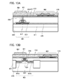
- FIGS. 8A and 8B are timing charts showing an example of driving the semiconductor memory device illustrated in FIG. 6 .
- the case where data is sequentially written into the memory cells 300 of the M-th row and then the written data is read is described as an example; however, one embodiment is not limited to this case.
- the potential of the M-th word line WL_M is set at VH and the potentials of the other word lines WL_other are set at VL as illustrated in FIG. 8A .
- VH is a potential higher than a reference potential (e.g., the ground potential) and, for example, is a high power supply potential.
- VL is a potential lower than or equal to the reference potential and, for example, is a low power supply potential.
- the transistor 311 is turned on and the potential of one of the pair of electrodes of the capacitor 313 becomes equal to the potential of the corresponding bit line BL.
- the transistor 311 is turned off and the gate of the transistor 312 becomes floating, so that the potential of the gate of the transistor 312 is held.
- Data can be written into all the memory cells 300 by performing the above operation row by row.
- the potentials of all the word lines WL are set at VL
- the potential of the M-th capacitor line CL_M is set at VL
- the potentials of the other capacitor lines CL_other are set at VH as illustrated in FIG. 8B .
- the resistance value between the source and the drain of the transistor 312 depends on the gate voltage of the transistor 312 .
- a potential corresponding to the amount of current flowing between the source and the drain of the transistor 312 can be read from the memory cell 300 as data.
- Data can be read from all the memory cells 300 by repeatedly performing the above operation row by row.
- the above is description of an example of a method for driving the semiconductor memory device illustrated in FIG. 6 .
- a data holding period can be made longer, and even when supply of the power supply voltage is stopped, data can be held.
- the transistor with extremely low off-state current is used for a transistor which controls writing and holding of data in the memory circuit 109 and the memory circuit 111 , power gating can be carried out, and a processor with low power consumption can be manufactured.
- FIG. 9 is a flow chart showing operation of the processor 100 .
- FIGS. 10A to 10C each show a relation between overhead and a power-off period in the processor 100 . Note that in each of FIGS. 10A to 10C , the horizontal axis indicates time, and the vertical axis indicates power consumption.
- Condition 1 is followed by Condition 2 and Condition 3.
- Condition 3 has the lowest speeds, which is followed by Condition 2 and Condition 1.
- the processor 100 (in particular, the arithmetic circuit 105 and the cache memory 107 ) operates at a constant speed. This operation is referred to as normal operation (step S_ 20 ) for convenience. Note that in the processor 100 under normal operation, the power supply voltage is supplied to the arithmetic circuit 105 and the cache memory 107 .
- the temperature detection circuit 113 detects the temperature of the memory circuit 109
- the temperature detection circuit 115 detects the temperature of the memory circuit 111 (step S_ 21 ). Detection of the temperatures enables overhead at the time of transferring data to the memory circuit 109 and the memory circuit 111 to be calculated (estimated). Specifically, overhead at the time when data obtained by the arithmetic circuit 105 and data stored in the cache memory 107 are written to nonvolatile memories included in the circuit 109 and the memory circuit 111 can be calculated.
- step S_ 22 whether a period during which supply of power to the arithmetic circuit 105 and the cache memory 107 is stopped can be secured or not is determined. This determination depends on the relation between the operation speeds of the arithmetic circuit 105 and the cache memory 107 and the temperature data of overhead or the like, which is estimated from the detected temperatures.
- a power-off period can be secured, regardless of any temperature of the memory circuit 111 , as long as overhead can be estimated and the relation a+b ⁇ c can be satisfied in the operation (see FIGS. 10A , 10 B, and 10 C).
- the power-off periods with respect to the arithmetic circuit 105 and the cache memory 107 can be secured, the data obtained by the arithmetic circuit 105 and the data stored in the cache memory 107 are transferred to the memory circuit 109 and the memory circuit 111 before the power-off periods start. Specifically, the data is written to the nonvolatile memories included in the memory circuit 109 and the memory circuit 111 (step S_ 23 ). Note that in the case where the power-off periods with respect to the arithmetic circuit 105 and the cache memory 107 are not be secured, the normal operation continues (step S_ 20 ).
- the power supply control switch provided between the arithmetic circuit 105 and the power supply and the power supply control switch provided between the cache memory 107 and the power supply are turned off, whereby supply of power to the arithmetic circuit 105 and the cache memory 107 is stopped (step S_ 24 ).
- step S_ 25 whether restoring of the written data is needed or not is determined. This determination state lasts until the arithmetic circuit 105 and the cache memory 107 are made to operate again. In the case where the arithmetic circuit 105 and the cache memory 107 are not made to operate again and restoring of the data is not necessary, the power gate remains off. Thus, power is not supplied to the arithmetic circuit 105 and the cache memory 107 until the arithmetic circuit 105 and the cache memory 107 are made to operate again.
- step S_ 26 In the case where the restoring of the data is needed, e.g., the case where the arithmetic circuit 105 and the cache memory 107 operate again, before resuming the operation, the power gate is turned on, so that supply of power to the arithmetic circuit 105 and the cache memory 107 is restarted (step S_ 26 ).
- step S_ 27 the transferred data is read out from the nonvolatile memories and restored in the arithmetic circuit and the cache memory (step S_ 27 ), and the normal operation is carried out again (step S_ 28 ).
- regions represented as “a” and “b” mean overhead at the time of writing or reading data to/from the nonvolatile memories included in the memory circuit 109 and the memory circuit 111 .
- a region represented as “c” means power which can be reduced by power gating.
- the amount of overhead is increased as the temperatures of the memory circuit 109 and the memory circuit 111 are increased. In other words, the amount of overhead under Condition 1 is smallest, which is followed by those of Condition 2 and Condition 3 in this order.
- a power-off period is determined on the basis of the amount of overhead of Condition 3 which has the highest temperatures of the memory circuit 109 and the memory circuit 111 , and a power-off period cannot be set except the above determined period.
- supply of power cannot be stopped (see FIGS. 16A to 16C ).
- the temperature data of the memory circuit 109 and the memory circuit 111 can be calculated by the temperature detection circuit 113 and the temperature detection circuit 115 ; overhead at the time when data obtained by the arithmetic circuit 105 and data stored in the cache memory 107 are held in the memory circuit 109 and the memory circuit 111 (specifically, overhead at the time of writing or reading data to/from the nonvolatile memories) can be estimated. Therefore, even under Condition 1 or Condition 2 where the supply of power cannot be stopped by the power gating conducted in accordance with the flow chart shown in FIG. 15 , a period during which power supply is stopped (power-off period) is set, and supply of the power supply voltage to the arithmetic circuit 105 and the cache memory 107 can be stopped ( FIGS. 10A and 10B ).
- the power-off periods with respect to the arithmetic circuit 105 and the cache memory 107 can be set, regardless of the operation speed of the processor 100 .
- a power-off period can be set even under high speed operation where it is difficult to provide a power-off period, and thus, power consumption can be reduced.
- the processor 100 can achieve low power consumption.
- the temperature of the memory circuit is detected, whereby a period during which supply of power to the circuit block is stopped can be optimally set in accordance with temperature dependency of overhead of the memory circuit, regardless of the operation speed. Therefore, in the semiconductor device which is one embodiment of the present invention, a period during which supply of power to the circuit block is stopped can be set, regardless of the operation speed; accordingly, power consumption can be favorably reduced.
- FIGS. 11A to 11C are not to scale in some cases.
- the transistor illustrated in FIG. 11A includes a semiconductor layer 711 , an insulating layer 714 , a conductive layer 715 , insulating layers 716 a and 716 b , an insulating layer 717 , conductive layers 718 a and 718 b , and an insulating layer 719 .
- the semiconductor layer 711 is positioned over an element formation layer 700 with the insulating layer 701 interposed therebetween. Note that the semiconductor layer 711 is not necessarily provided over the insulating layer 701 and may be provided directly on the element formation layer 700 .
- the semiconductor layer 711 includes regions 709 a and 709 b which are separated from each other and to which dopant is added, and regions 712 a and 712 b which are separated from each other and to which the dopant is added. Between the regions 709 a and 709 b , a channel formation region 713 is provided.
- the regions 712 a and 712 b to which the dopant is added has higher dopant concentration and lower resistivity than the regions 709 a and 709 b to which the dopant is added.
- the regions 712 a and 712 b function as a source region and a drain region. As in the semiconductor layer 711 , the resistivity is gradually changed, whereby the electric-field concentration in the vicinity of the drain region can be reduced. Thus, a fluctuation in the threshold voltage, a breakdown of the transistor, and the like can be suppressed.
- the insulating layer 714 is positioned over part of the semiconductor layer 711 .
- the conductive layer 715 overlaps with the semiconductor layer 711 with the insulating layer 714 interposed therebetween.
- the insulating layer 716 a is provided in contact with one of a pair of side surfaces of the conductive layer 715 .
- the insulating layer 716 b is provided in contact with the other thereof.
- the insulating layer 717 is positioned over the conductive layer 715 . Note that the insulating layer 717 is not necessarily provided as shown in FIG. 11B .
- the conductive layers 718 a and 718 b are in contact with the regions 712 a and 712 b , respectively. Further, the conductive layers 718 a and 718 b are in contact with a side surface of the insulating layer 716 a and that of the insulating layer 716 b , respectively.
- the insulating layer 719 is positioned over the conductive layers 718 a and 718 b.
- the conductive layers 718 a and 718 b and the insulating layer 719 are formed in such a manner that a stack of a conductive film and an insulating layer is subjected to a planarization treatment (e.g., CMP treatment or etchback treatment), for example.
- a planarization treatment e.g., CMP treatment or etchback treatment
- providing the insulating layer 717 as in the transistor in FIG. 11A can prevent short circuit between the conductive layer 715 and the conductive layers 718 a and 718 b because they are not in contact with each other after the planarization treatment.
- the transistor in FIG. 11C includes a conductive layer 751 , an insulating layer 752 , an insulating layer 753 , a semiconductor layer 754 , conductive layers 755 a and 755 b , an insulating layer 756 , and an insulating layer 757 .
- the conductive layer 751 is positioned over an element formation layer 750 .
- the insulating layer 752 is provided over the element formation layer 750 .
- Surfaces of the insulating layer 752 and the conductive layer 751 are preferably flat.
- the conductive layer 751 and the insulating layer 752 are formed, for example, by planarization treatment (e.g., CMP treatment or etchback treatment) performed on a stack of a conductive film and an insulating layer.
- planarization treatment e.g., CMP treatment or etchback treatment
- the insulating layer 753 is positioned over the conductive layer 751 and the insulating layer 752 .
- the semiconductor layer 754 overlaps with the conductive layer 751 with the insulating layer 753 interposed therebetween.
- the conductive layers 755 a and 755 b are separated from each other and electrically connected to the semiconductor layer 754 .
- the distance between the conductive layers 755 a and 755 b corresponds to the channel length of the transistor and is preferably shorter than 50 nm, for example.
- the distance between the conductive layers 755 a and 755 b can be made shorter than 50 nm in such a manner that part of a conductive film is etched using a resist mask formed by electron beam exposure.
- a resist mask is formed by ultraviolet light exposure, the resist mask is subjected to slimming treatment, and then part of the conductive film is etched with use of the mask.
- a pair of conductive layers may be provided between the insulating layer 756 and the conductive layers 755 a and 755 b .
- the distance between such a pair of conductive layers is preferably larger than that of the conductive layers 755 a and 755 b .
- the electric resistance of the pair of conductive layers is preferably lower than that of the conductive layers 755 a and 755 b .
- the insulating layer 757 is positioned over the semiconductor layer 754 to cover an upper surface of the semiconductor layer 754 .
- Each of the components is not limited to a single layer and may be a stack of layers.
- the insulating layer 701 is a base layer.
- the insulating layer 701 can be, for example, a layer containing a material such as silicon oxide, silicon nitride, silicon oxynitride, silicon nitride oxide, aluminum oxide, aluminum nitride, aluminum oxynitride, aluminum nitride oxide, or hafnium oxide.
- the insulating layer 752 can be a layer containing a material similar to that of the insulating layer 701 .
- Each of the semiconductor layers 711 and 754 functions as a layer in which a channel of the transistor is formed (also referred to as channel formation layer).
- a semiconductor layer including an oxide semiconductor (also referred to as oxide semiconductor layer) can be used, for example.
- An oxide semiconductor film may be in a non-single-crystal state, for example.
- the non-single-crystal state is, for example, structured by at least one of c-axis aligned crystal (CAAC), polycrystal, microcrystal, and an amorphous part.
- CAAC c-axis aligned crystal
- the density of defect states of an amorphous part is higher than those of microcrystal and CAAC.
- the density of defect states of microcrystal is higher than that of CAAC.
- CAAC-OS c-axis aligned crystalline oxide semiconductor
- an oxide semiconductor film may include a CAAC-OS.
- CAAC-OS for example, c-axes are aligned, and a-axes and/or b-axes are not macroscopically aligned.
- an oxide semiconductor film may include microcrystal.
- an oxide semiconductor including microcrystal is referred to as a microcrystalline oxide semiconductor.
- a microcrystalline oxide semiconductor film includes microcrystal (also referred to as nanocrystal) with a size greater than or equal to 1 nm and less than 10 nm, for example.
- an oxide semiconductor film may include an amorphous part.
- an oxide semiconductor including an amorphous part is referred to as an amorphous oxide semiconductor.
- An amorphous oxide semiconductor film for example, has disordered atomic arrangement and no crystalline component.
- an amorphous oxide semiconductor film is, for example, absolutely amorphous and has no crystal part.
- an oxide semiconductor film may be a mixed film including any of a CAAC-OS, a microcrystalline oxide semiconductor, and an amorphous oxide semiconductor.
- the mixed film for example, includes a region of an amorphous oxide semiconductor, a region of a microcrystalline oxide semiconductor, and a region of a CAAC-OS.
- the mixed film may have a stacked structure including a region of an amorphous oxide semiconductor, a region of a microcrystalline oxide semiconductor, and a region of a CAAC-OS, for example.
- an oxide semiconductor film may be in a single-crystal state, for example.
- An oxide semiconductor film preferably includes a plurality of crystal parts.
- a c-axis is preferably aligned in a direction parallel to a normal vector of a surface where the oxide semiconductor film is formed or a normal vector of a surface of the oxide semiconductor film. Note that, among crystal parts, the directions of the a-axis and the b-axis of one crystal part may be different from those of another crystal part.
- An example of such an oxide semiconductor film is a CAAC-OS film.
- a crystal part in the CAAC-OS film fits inside a cube whose one side is less than 100 nm.
- TEM transmission electron microscope
- a boundary between crystal parts in the CAAC-OS film is not clearly detected.
- TEM transmission electron microscope
- a grain boundary in the CAAC-OS film is not clearly found.
- a c-axis is aligned in a direction parallel to a normal vector of a surface where the CAAC-OS film is formed or a normal vector of a surface of the CAAC-OS film.
- metal atoms are arranged in a triangular or hexagonal configuration when seen from the direction perpendicular to the a-b plane, and metal atoms are arranged in a layered manner or metal atoms and oxygen atoms are arranged in a layered manner when seen from the direction perpendicular to the c-axis.
- a term “perpendicular” includes a range from 80° to 100°, preferably from 85° to 95°.
- a term “parallel” includes a range from ⁇ 10° to 10°, preferably from ⁇ 5° to 5°.
- the CAAC-OS film distribution of crystal parts is not necessarily uniform.
- the proportion of crystal parts in the vicinity of the surface of the oxide semiconductor film is higher than that in the vicinity of the surface where the oxide semiconductor film is formed in some cases.
- crystallinity of the crystal part in a region to which the impurity is added is lowered in some cases.
- the directions of the c-axes may be different from each other depending on the shape of the CAAC-OS film (the cross-sectional shape of the surface where the CAAC-OS film is formed or the cross-sectional shape of the surface of the CAAC-OS film).
- the film deposition is accompanied with the formation of the crystal parts or followed by the formation of the crystal parts through crystallization treatment such as heat treatment.
- the c-axes of the crystal parts are aligned in the direction parallel to a normal vector of the surface where the CAAC-OS film is formed or a normal vector of the surface of the CAAC-OS film.
- the transistor In a transistor using the CAAC-OS film, change in electric characteristics due to irradiation with visible light or ultraviolet light is small. Thus, the transistor has high reliability.
- metal oxide containing zinc and one or both of indium and gallium, metal oxide containing another metal element instead of part or all of gallium in the given metal oxide, or the like can be given.
- In-based metal oxide Zn-based metal oxide, In—Zn-based metal oxide, In—Ga—Zn-based metal oxide, or the like can be used as the metal oxide.
- (gallium) in the In—Ga—Zn-based metal oxide may be used.
- a metal element that is capable of combining with more oxygen atoms than gallium can be used.
- one or more elements of titanium, zirconium, hafnium, germanium, and tin can be used.
- one or more elements of lanthanum, cerium, praseodymium, neodymium, samarium, europium, gadolinium, terbium, dysprosium, holmium, erbium, thulium, ytterbium, and lutetium may be used. These metal elements function as a stabilizer.
- the additive amount of such a metal element is determined so that the metal oxide can function as a semiconductor.
- a metal element that is capable of combining with more oxygen atoms than gallium is used and oxygen is supplied to a metal oxide, oxygen defects in the metal oxide can be reduced.
- In—Sn—Zn-based metal oxide In—Sn—Zn-based metal oxide is obtained.
- titanium is used instead of part of Ga (gallium) contained in the In—Ga—Zn-based metal oxide, In—Ti—Ga—Zn-based metal oxide is obtained.
- the oxide semiconductor layer can be highly purified, for example, in the following manner: dehydration or dehydrogenation is performed so that impurities such as hydrogen, water, a hydroxyl group, and a hydride (also referred to as hydrogen compound) are removed from the oxide semiconductor layer, and oxygen is supplied to the oxide semiconductor layer.
- impurities such as hydrogen, water, a hydroxyl group, and a hydride (also referred to as hydrogen compound) are removed from the oxide semiconductor layer, and oxygen is supplied to the oxide semiconductor layer.
- a layer containing oxygen is used as the layer in contact with the oxide semiconductor layer, and heat treatment is performed; thus, the oxide semiconductor layer can be highly purified.
- heat treatment is preferably performed as appropriate at least after the step of forming the semiconductor layer 711 .
- the temperature of the heat treatment is higher than or equal to 300° C. and lower than or equal to 700° C., or lower than the strain point of the substrate.
- the heat treatment can be performed under reduced pressure, a nitrogen atmosphere, an oxygen atmosphere, a rare gas atmosphere, or the like. Note that the heat treatment may be performed more than once.
- heat treatment is preferably performed at least after the semiconductor layer 754 is formed or after the insulating layer 757 is formed; alternatively, heat treatment is performed plural times, i.e., after the semiconductor layer 754 is formed and after the insulating layer 757 is formed.
- the temperature of the heat treatment is higher than or equal to 300° C. and lower than or equal to 700° C., or lower than the strain point of the substrate.
- the heat treatment can be performed under reduced pressure, a nitrogen atmosphere, an oxygen atmosphere, a rare gas atmosphere, or the like.
- the oxide semiconductor layer that has just been formed is preferably supersaturated with oxygen so that the proportion of oxygen is higher than that in the stoichiometric composition.
- the oxide semiconductor layer is preferably formed under the condition where the proportion of oxygen in a deposition gas is high, and particularly in an oxygen atmosphere (e.g., oxygen gas: 100%).
- the oxide semiconductor film may be formed by a sputtering method at the substrate temperature of higher than or equal to 100° C. and lower than or equal to 500° C., preferably higher than or equal to 200° C. and lower than or equal to 350° C. In such a manner, a CAAC-OS layer can be easily formed.
- an insulating layer e.g., the insulating layers 701 , 714 , 753 , and 757 ) which contains excess oxygen may be provided as the insulating layer in contact with the oxide semiconductor layer.
- the insulating layer containing excess oxygen can be formed as follows: the insulating layer is deposited using a sputtering method under the deposition conditions such that a large amount of oxygen is contained in the film.
- oxygen may be added by an ion implantation method, an ion doping method, or plasma treatment.
- oxygen may be added to the oxide semiconductor layer.
- the amount of moisture remaining in a deposition chamber is preferably small. Therefore, an entrapment vacuum pump is preferably used in the sputtering apparatus. Further, a cold trap may be used.
- a heat treatment apparatus to be used for the heat treatment, and a rapid thermal annealing (RTA) apparatus such as a gas rapid thermal annealing (GRTA) apparatus or a lamp rapid thermal annealing (LRTA) apparatus may be used.
- RTA rapid thermal annealing
- GRTA gas rapid thermal annealing
- LRTA lamp rapid thermal annealing
- another heat treatment apparatus such as an electric furnace may be used.
- a high-purity oxygen gas, a high-purity N 2 O gas, or ultra-dry air (having a dew point of ⁇ 40° C. or lower, preferably ⁇ 60° C. or lower) is preferably introduced in the furnace where the heat treatment has been performed while the heating temperature is being maintained or being decreased.
- the oxygen gas or the N 2 O gas do not contain water, hydrogen, or the like.
- the purity of the oxygen gas or the N 2 O gas which is introduced into the heat treatment apparatus is preferably 6N or higher, more preferably 7N or higher. That is, the impurity concentration of the oxygen gas or the N 2 O gas is preferably 1 ppm or lower, more preferably 0.1 ppm or lower.
- oxygen is supplied to the oxide semiconductor layer, and defects due to oxygen vacancies in the oxide semiconductor layer can be reduced.
- introduction of a high-purity oxygen gas, a high-purity N 2 O gas, or ultra-dry air may be performed at the time of the above heat treatment.
- the hydrogen concentration of the highly purified oxide semiconductor layer measured by secondary ion mass spectrometry (also referred to as SIMS), is 5 ⁇ 10 19 atoms/cm 3 or lower, preferably 5 ⁇ 10 18 atoms/cm 3 or lower, more preferably 5 ⁇ 10 17 atoms/cm 3 or lower.
- the carrier density of the oxide semiconductor layer in a transistor can be lower than 1 ⁇ 10 14 /cm 3 , preferably lower than 1 ⁇ 10 12 /cm 3 , further preferably lower than 1 ⁇ 10 11 /cm 3 .
- Such a low carrier density can reduce the off-state current of the transistor per micrometer of channel width to 1 ⁇ 10 ⁇ 19 A (100 zA) or less, preferably 1 ⁇ 10 ⁇ 22 A (100 yA) or less.
- the off-state current of the transistor be as low as possible; the lowest value of the off-state current of the transistor is estimated to be about 1 ⁇ 10 ⁇ 30 A/ ⁇ m.
- the dopant contained in the regions 712 a and 712 b it is possible to use an element of Group 13 in the periodic table (e.g., boron), an element of Group 15 in the periodic table (e.g., one or more of nitrogen, phosphorus, and arsenic), and/or a rare gas element (e.g., one or more of helium, argon, and xenon), for example.
- the dopant can be selected from at least one of these groups.
- the dopant is added with use of the conductive layer 715 as a mask, and at least the insulating layers 716 a and 716 b are formed.
- the dopant is added again with use of the conductive layer 715 and the insulating layers 716 a and 716 b as a mask, so that the regions 709 a and 709 b , the regions 712 a and 712 b , and the channel formation region 713 can be formed in a self-aligned manner.
- Each of the insulating layers 714 and 753 functions as a gate insulating layer of the transistor.
- a layer containing a material such as silicon oxide, silicon nitride, silicon oxynitride, silicon nitride oxide, aluminum oxide, aluminum nitride, aluminum oxynitride, aluminum nitride oxide, or hafnium oxide can be used.
- Each of the conductive layers 715 and 751 functions as a gate electrode of the transistor.
- a layer containing a metal material such as molybdenum, titanium, chromium, tantalum, magnesium, silver, tungsten, aluminum, copper, neodymium, or scandium can be used. Note that each of the conductive layers 715 and 751 also functions as a gate wiring.
- Each of the insulating layers 716 a , 716 b , and 717 can be, for example, a layer containing a material such as silicon oxide, silicon nitride, silicon oxynitride, silicon nitride oxide, aluminum oxide, aluminum nitride, aluminum oxynitride, aluminum nitride oxide, or hafnium oxide.
- Each of the conductive layers 718 a and 718 b and the conductive layers 755 a and 755 b functions as a source electrode or a drain electrode of the transistor.
- Each of the conductive layers 718 a and 718 b and the conductive layers 755 a and 755 b can be, for example, a layer containing a metal material such as molybdenum, titanium, chromium, tantalum, magnesium, silver, tungsten, aluminum, copper, neodymium, scandium, or ruthenium. Note that each of the conductive layers 718 a and 718 b and the conductive layers 755 a and 755 b also serves as a source wiring or a drain wiring.
- the insulating layers 719 and 757 each function as a protective layer.
- Each of the insulating layers 719 and 757 can be, for example, a layer containing a material such as silicon oxide, silicon nitride, silicon oxynitride, silicon nitride oxide, aluminum oxide, aluminum nitride, aluminum oxynitride, aluminum nitride oxide, or hafnium oxide.
- the semiconductor layer 711 is a 20-nm-thick In—Ga—Zn-based oxide semiconductor layer
- the insulating layer 714 is a 20-nm-thick silicon oxynitride layer
- the conductive layer 715 is a stack of a 30-nm-thick tantalum nitride layer and a 200-nm-thick tungsten layer
- each of the conductive layers 718 a and 718 b is a 30-nm-thick tungsten layer.
- phosphorus is added to form the regions 712 a and 712 b .
- the amount of added phosphorus is 1 ⁇ 10 15 cm ⁇ 2 and the acceleration voltage is 30 kV.
- the channel length is 5 ⁇ m and the channel width is 10 ⁇ m.
- the horizontal axis indicates the gate voltage Vg and the vertical axis indicates the drain current Id or the field-effect mobility ⁇ FE.
- the field-effect mobility is about 20 cm 2 /Vs
- the off-state current is under the detection limit
- the threshold voltage is higher than or equal to 0 V.
- the value of the on-state resistance of the transistor exhibiting the Id-Vg characteristics shown in FIG. 12 is calculated with reference to following the formula (1).
- the gate capacitance Cox is 1.82 ⁇ 10 ⁇ 3 F/m 2 .
- the mobility of the transistor ⁇ FE is 20 cm 2 /Vs and the threshold voltage Vth is 0.6 V according to the data in FIG. 12 and when the gate voltage Vg is 3.3 V and the drain voltage Vd is 1.8 V as the specification example of the memory circuit, the on-state resistance Rd is 76.3 k ⁇ from the above formula (1).
- FIGS. 13A and 13B are cross-sectional schematic views illustrating the structure examples of the memory circuit according to this embodiment. Note that one embodiment of the present invention is not limited thereto; a memory circuit may be formed using the transistors illustrated in FIGS. 11B and 11C .
- the memory circuit illustrated in FIG. 13A includes a transistor 801 including a single crystal silicon layer 813 that is a channel formation layer, a transistor 802 that is stacked over the transistor 801 with insulating layers 815 to 817 placed therebetween and has the same structure as that illustrated in FIG. 11A , and a capacitor 803 formed through manufacturing steps of the transistor 801 .
- the transistor 801 is a p-channel transistor
- the transistor 802 is an n-channel transistor. Note that the description of the transistor illustrated in FIG. 11A can apply to the transistor 802 as appropriate.
- the single crystal silicon layer 813 is provided over a substrate 810 with an insulating layer (also referred to as BOX layer) 811 placed therebetween.
- the transistor 801 may be composed of a semiconductor region 823 surrounded by a buried insulating region 822 in a single crystal semiconductor substrate 820 , instead of using the substrate 810 , the insulating layer 811 , and the single crystal silicon layer 813 .
- impurity regions 825 a and 825 b whose conductivity is n-type or p-type are provided.
- the insulating layer 815 serves as a protective layer.
- the insulating layer 816 functions both as a protective layer and as a planarization layer.
- the insulating layer 817 functions as a base layer.
- Each of the insulating layers 815 to 817 can be a layer containing a material similar to that of the insulating layer 701 illustrated in FIG. 11A .
- a conductive layer 818 functioning as a source electrode or a drain electrode of the transistor 802 is connected to a conductive layer 814 functioning as a gate electrode of the transistor 801 .
- the conductive layer 818 and the conductive layer 814 may be connected to each other through a plurality of conductive layers.
- the memory circuit may have the structure as shown in FIG. 13B in which the conductive layer 824 serving as the gate electrode of the transistor 801 has a direct contact with the conductive layer 818 .
- the conductive layer 818 may be electrically connected to the conductive layer 814 through another conductive layer (e.g., a conductive layer 826 ) without direct contact between the conductive layers 818 and 814 (see FIG. 13A ).
- the conductive layer 826 is formed in the following manner: a layer including a material similar to that of the conductive layers 718 a and 718 b of the transistor illustrated in FIG. 11A ; and the layer is planarized or etched.
- the transistor 802 the transistor with extremely low off-state current can be used.
- the conductive layer 818 corresponds to the conductive layer 718 a of the transistor illustrated in FIG. 11A .
- the capacitor 803 has a structure in which a dielectric is provided between a pair of conductive layers.
- One of the pair of conductive layers is the conductive layer 818
- the other conductive layer is the conductive layer 821
- the dielectric is the insulating layer 819 .
- the insulating layer 819 corresponds to the insulating layer 719 of the transistor illustrated in FIG. 11A .
- the conductive layer 821 has a structure similar to that of the conductive layer 818 .
- a transistor with extremely low off-state current can be formed by using an oxide semiconductor.
- the transistor including an oxide semiconductor is applied to a transistor included in a volatile memory, whereby the volatile memory can function as a nonvolatile memory which can be applied to a semiconductor memory device of a memory circuit included in the semiconductor device which is one embodiment of the present invention.
- FIGS. 14A to 14F illustrates specific examples of an electronic device including the semiconductor device
- the electronic device illustrated in FIG. 14A is an example of a personal digital assistant.
- the electronic device illustrated in FIG. 14A includes a housing 1011 and a panel 1012 , a button 1013 , and a speaker 1014 which are provided for the housing 1011 .
- the housing 1011 may be provided with a connection terminal for connecting the electronic device to an external device and a button for operating the electronic device.
- the panel 1012 is a display panel (display).
- the panel 1012 preferably has a function of a touch panel.
- the button 1013 is provided for the housing 1011 .
- pressing the button 1013 can turn on or off the electronic device.
- the speaker 1014 is provided for the housing 1011 .
- the speaker 1014 has a function of outputting sound.
- the housing 1011 may be provided with a microphone, in which case the electronic device in FIG. 14A can function as a telephone, for example.
- the electronic device in FIG. 14A includes the semiconductor device including the processor described in the above embodiment inside the housing 1011 .
- the electronic device illustrated in FIG. 14A functions as one or more of a telephone set, an e-book reader, a personal computer, and a game machine, for example.
- the electronic device illustrated in FIG. 14B is an example of a foldable information terminal.
- the electronic device illustrated in FIG. 14B includes a housing 1021 a , a housing 1021 b , a panel 1022 a provided for the housing 1021 a , a panel 1022 b provided for the housing 1021 b , a hinge 1023 , a button 1024 , a connection terminal 1025 , a storage medium inserting portion 1026 , and a speaker 1027 .
- the housing 1021 a and the housing 1021 b are connected by the hinge 1023 .
- the panels 1022 a and 1022 b are display panels (displays).
- the panels 1022 a and 1022 b preferably have a function of a touch panel.
- the electronic device in FIG. 14B includes the hinge 1023 , it can be folded so that the panels 1022 a and 1022 b face each other.
- the button 1024 is provided for the housing 1021 b .
- the housing 1021 a may also be provided with the button 1024 .
- the button 1024 which functions as a power button is provided and pushed, supply of a power voltage to the electronic device can be controlled.
- connection terminal 1025 is provided for the housing 1021 a .
- the housing 1021 b may be provided with the connection terminal 1025 .
- a plurality of connection terminals 1025 may be provided on one or both of the housings 1021 a and the housing 1021 b .
- the connection terminal 1025 is a terminal for connecting the electronic device illustrated in FIG. 14B to another device.
- the storage media inserting portion 1026 is provided for the housing 1021 a .
- the storage medium insertion portion 1026 may be provided on the housing 1021 b .
- the plurality of recording medium insertion portions 1026 may be provided for one or both of the housings 1021 a and 1021 b .
- a card-type recording medium is inserted into the recording medium insertion portion so that data can be read to the electronic device from the card-type recording medium or data stored in the electronic device can be written to the card-type recording medium.
- the speaker 1027 is provided for the housing 1021 b .
- the speaker 1027 outputs sound. Note that the speaker 1027 may be provided for the housing 1021 a.
- housing 1021 a or the housing 1021 b may be provided with a microphone, in which case the electronic device in FIG. 14B can function as a telephone, for example.
- the electronic device in FIG. 14B includes the semiconductor device including the processor described in Embodiment 1 inside the housing 1021 a or the housing 1021 b.
- the electronic device illustrated in FIG. 14B functions as one or more of a telephone set, an e-book reader, a personal computer, and a game machine, for example.
- the electronic device illustrated in FIG. 14C is an example of a stationary information terminal.
- the stationary information terminal illustrated in FIG. 14C includes a housing 1031 , and a panel 1032 , a button 1033 , and a speaker 1034 that are provided for the housing 1031 .
- the panel 1032 is a display panel (display).
- the panel 1032 preferably has a function of a touch panel.
- a panel similar to the panel 1032 may be provided for a deck portion 1035 of the housing 1031 .
- This panel preferably has a function of a touch panel.
- the housing 1031 may be provided with one or more of a ticket slot from which a ticket or the like is dispensed, a coin slot, and a bill slot.
- the button 1033 is provided for the housing 1031 .
- the button 1033 is a power button
- supply of a power voltage to the electronic device can be controlled by pressing the button 1033 .
- the speaker 1034 is provided for the housing 1031 .
- the speaker 1034 has a function of outputting sound.
- the electronic device in FIG. 14C includes the semiconductor device including the processor described in Embodiment 1 inside the housing 1031 .
- the electronic device illustrated in FIG. 14C has, for example, a function as an automated teller machine, an information communication terminal for ordering a ticket or the like (also referred to as a multi-media station), or a game machine.
- FIG. 14D illustrates an example of a stationary information terminal.
- the electronic device illustrated in FIG. 14D includes a housing 1041 , a panel 1042 incorporated in the housing 1041 , a support 1043 for supporting the housing 1041 , a button 1044 , a connection terminal 1045 , and a speaker 1046 .
- connection terminal for connecting the housing 1041 to an external device may be provided.
- the panel 1042 has a function as a display panel (display).
- the button 1044 is provided for the housing 1041 .
- the button 1044 is a power button
- supply of a power voltage to the electronic device can be controlled by pressing the button 1044 .
- the connection terminal 1045 is provided for the housing 1041 .
- the connection terminal 1045 is a terminal for connecting the electronic device illustrated in FIG. 14D to another device.
- the panel 1042 can display an image corresponding to a data signal input from the personal computer.
- a displayed image of the other electronic device can be enlarged, so that a plurality of viewers can easily see the image at the same time.
- the speaker 1046 is provided for the housing 1041 .
- the speaker 1046 has a function of outputting sound.
- the electronic device in FIG. 14D includes the semiconductor device including the processor described in Embodiment 1 inside the housing 1041 .
- the electronic device illustrated in FIG. 14D functions as, for example, an output monitor, a personal computer, and/or a television set.
- FIG. 14E illustrates an example of an electric refrigerator-freezer.
- the electronic device illustrated in FIG. 14E includes a housing 1051 , a refrigerator door 1052 , and a freezer door 1053 .
- the electronic device in FIG. 14E includes the semiconductor device including the processor described in Embodiment 1 inside the housing 1051 .
- supply of a power voltage to the semiconductor device in the housing 1051 can be controlled in response to opening and closing of the refrigerator door 1052 and the freezer door 1053 , for example.
- FIG. 14F illustrates an example of an air conditioner.
- the electronic device illustrated in FIG. 14F includes an indoor unit 1060 and an outdoor unit 1064 .
- the indoor unit 1060 includes a housing 1061 and a ventilation duct 1062 .
- the electronic device in FIG. 14F includes the semiconductor device including the processor described in Embodiment 1 inside the housing 1061 .
- supply of a power voltage to the semiconductor device in the housing 1061 can be controlled in response to a signal from a remote controller, for example.
- the separated air conditioner including the indoor unit and the outdoor unit is shown in FIG. 14F as an example, it may be an air conditioner in which the functions of an indoor unit and an outdoor unit are integrated in one housing.
- Examples of the electronic devices are not limited to the above, and the semiconductor device including the processor described in the above embodiment can also be applied to a high-frequency heating apparatus such as a microwave oven, an electric rice cooker, and the like.
- an electronic device having superiority in cutting low power consumption can be manufactured.
Landscapes
- Engineering & Computer Science (AREA)
- Power Engineering (AREA)
- Semiconductor Memories (AREA)
- Thin Film Transistor (AREA)
- Semiconductor Integrated Circuits (AREA)
- Power Sources (AREA)
- Non-Volatile Memory (AREA)
- Metal-Oxide And Bipolar Metal-Oxide Semiconductor Integrated Circuits (AREA)
Priority Applications (2)
| Application Number | Priority Date | Filing Date | Title |
|---|---|---|---|
| US14/670,525 US9293174B2 (en) | 2012-03-07 | 2015-03-27 | Semiconductor device |
| US15/070,145 US9812178B2 (en) | 2012-03-07 | 2016-03-15 | Semiconductor device |
Applications Claiming Priority (2)
| Application Number | Priority Date | Filing Date | Title |
|---|---|---|---|
| JP2012-050085 | 2012-03-07 | ||
| JP2012050085 | 2012-03-07 |
Related Child Applications (1)
| Application Number | Title | Priority Date | Filing Date |
|---|---|---|---|
| US14/670,525 Continuation US9293174B2 (en) | 2012-03-07 | 2015-03-27 | Semiconductor device |
Publications (2)
| Publication Number | Publication Date |
|---|---|
| US20130235689A1 US20130235689A1 (en) | 2013-09-12 |
| US8995218B2 true US8995218B2 (en) | 2015-03-31 |
Family
ID=49114034
Family Applications (3)
| Application Number | Title | Priority Date | Filing Date |
|---|---|---|---|
| US13/783,573 Expired - Fee Related US8995218B2 (en) | 2012-03-07 | 2013-03-04 | Semiconductor device |
| US14/670,525 Expired - Fee Related US9293174B2 (en) | 2012-03-07 | 2015-03-27 | Semiconductor device |
| US15/070,145 Expired - Fee Related US9812178B2 (en) | 2012-03-07 | 2016-03-15 | Semiconductor device |
Family Applications After (2)
| Application Number | Title | Priority Date | Filing Date |
|---|---|---|---|
| US14/670,525 Expired - Fee Related US9293174B2 (en) | 2012-03-07 | 2015-03-27 | Semiconductor device |
| US15/070,145 Expired - Fee Related US9812178B2 (en) | 2012-03-07 | 2016-03-15 | Semiconductor device |
Country Status (2)
| Country | Link |
|---|---|
| US (3) | US8995218B2 (enExample) |
| JP (3) | JP2013214296A (enExample) |
Cited By (5)
| Publication number | Priority date | Publication date | Assignee | Title |
|---|---|---|---|---|
| US20140025978A1 (en) * | 2012-07-20 | 2014-01-23 | Semiconductor Energy Laboratory Co., Ltd. | Power supply control circuit and signal processing circuit |
| US9165668B1 (en) * | 2013-07-29 | 2015-10-20 | Western Digital Technologies, Inc. | Data retention monitoring using temperature history in solid state drives |
| US9293174B2 (en) * | 2012-03-07 | 2016-03-22 | Semiconductor Energy Laboratory Co., Ltd. | Semiconductor device |
| CN106227309A (zh) * | 2016-07-26 | 2016-12-14 | 深圳市金泰克半导体有限公司 | 一种具有散热功能的pcie接口固态硬盘及其实现方法 |
| US10445227B2 (en) | 2014-12-18 | 2019-10-15 | Semiconductor Energy Laboratory Co., Ltd. | Semiconductor device, sensor device, and electronic device |
Families Citing this family (27)
| Publication number | Priority date | Publication date | Assignee | Title |
|---|---|---|---|---|
| US9030232B2 (en) | 2012-04-13 | 2015-05-12 | Semiconductor Energy Laboratory Co., Ltd. | Isolator circuit and semiconductor device |
| KR102025722B1 (ko) | 2012-05-02 | 2019-09-26 | 가부시키가이샤 한도오따이 에네루기 켄큐쇼 | 온도 센서 회로, 및 온도 센서 회로를 사용한 반도체 장치 |
| WO2014077295A1 (en) | 2012-11-15 | 2014-05-22 | Semiconductor Energy Laboratory Co., Ltd. | Liquid crystal display device |
| JP6396671B2 (ja) | 2013-04-26 | 2018-09-26 | 株式会社半導体エネルギー研究所 | 半導体装置 |
| US9454923B2 (en) | 2013-05-17 | 2016-09-27 | Semiconductor Energy Laboratory Co., Ltd. | Semiconductor device |
| JP6072297B2 (ja) * | 2013-11-25 | 2017-02-01 | シャープ株式会社 | 半導体装置およびその書き込み方法 |
| KR102267237B1 (ko) * | 2014-03-07 | 2021-06-18 | 가부시키가이샤 한도오따이 에네루기 켄큐쇼 | 반도체 장치 및 전자 기기 |
| JP2016066065A (ja) | 2014-09-05 | 2016-04-28 | 株式会社半導体エネルギー研究所 | 表示装置、および電子機器 |
| US9971535B2 (en) | 2014-11-05 | 2018-05-15 | Industrial Technology Research Institute | Conversion method for reducing power consumption and computing apparatus using the same |
| US10706790B2 (en) | 2014-12-01 | 2020-07-07 | Semiconductor Energy Laboratory Co., Ltd. | Display device, display module including the display device, and electronic device including the display device or the display module |
| US9607676B2 (en) * | 2015-08-12 | 2017-03-28 | Avalanche Technology, Inc. | Method and apparatus for adjustment of current through a magnetoresistive tunnel junction (MTJ) based on temperature fluctuations |
| TWI753908B (zh) | 2016-05-20 | 2022-02-01 | 日商半導體能源硏究所股份有限公司 | 半導體裝置、顯示裝置及電子裝置 |
| CN109478883A (zh) | 2016-07-19 | 2019-03-15 | 株式会社半导体能源研究所 | 半导体装置 |
| US10120470B2 (en) | 2016-07-22 | 2018-11-06 | Semiconductor Energy Laboratory Co., Ltd. | Semiconductor device, display device and electronic device |
| JP7044495B2 (ja) | 2016-07-27 | 2022-03-30 | 株式会社半導体エネルギー研究所 | 半導体装置 |
| US10797706B2 (en) | 2016-12-27 | 2020-10-06 | Semiconductor Energy Laboratory Co., Ltd. | Semiconductor device |
| JP2018129374A (ja) * | 2017-02-07 | 2018-08-16 | ソニーセミコンダクタソリューションズ株式会社 | 半導体装置および半導体装置の製造方法 |
| JP7109973B2 (ja) * | 2018-04-13 | 2022-08-01 | 株式会社半導体エネルギー研究所 | 半導体装置 |
| JP6939837B2 (ja) | 2019-04-01 | 2021-09-22 | カシオ計算機株式会社 | 電源回路、電源制御方法、及び電源制御プログラム |
| JP6796681B2 (ja) * | 2019-05-13 | 2020-12-09 | ウィンボンド エレクトロニクス コーポレーション | 半導体記憶装置 |
| CN113870916B (zh) * | 2020-06-30 | 2024-03-26 | 长鑫存储技术有限公司 | 半导体装置 |
| CN113945293B (zh) | 2020-06-30 | 2023-04-18 | 长鑫存储技术有限公司 | 半导体装置 |
| CN111933070A (zh) * | 2020-07-27 | 2020-11-13 | 重庆惠科金渝光电科技有限公司 | 驱动电路以及显示装置 |
| KR102891516B1 (ko) * | 2020-11-02 | 2025-11-25 | 삼성전자 주식회사 | 전력 측정에 기초한 온도 검출 및 열 관리를 위한 방법 및 장치 |
| JP7810444B2 (ja) | 2021-03-31 | 2026-02-03 | 国立大学法人東北大学 | 半導体回路装置 |
| US12217793B2 (en) | 2021-11-16 | 2025-02-04 | Samsung Electronics Co., Ltd. | Data transfer circuits in nonvolatile memory devices and nonvolatile memory devices including the same |
| CN114698072B (zh) * | 2022-03-21 | 2024-04-26 | 沈阳中科奥维科技股份有限公司 | Wia-pa无线振动变送器的低功耗电路及控制方法 |
Citations (123)
| Publication number | Priority date | Publication date | Assignee | Title |
|---|---|---|---|---|
| JPS60198861A (ja) | 1984-03-23 | 1985-10-08 | Fujitsu Ltd | 薄膜トランジスタ |
| US4716551A (en) * | 1983-09-14 | 1987-12-29 | Nec Corporation | Semiconductor memory device with variable self-refresh cycle |
| JPS63210024A (ja) | 1987-02-24 | 1988-08-31 | Natl Inst For Res In Inorg Mater | InGaZn↓5O↓8で示される六方晶系の層状構造を有する化合物およびその製造法 |
| JPS63210023A (ja) | 1987-02-24 | 1988-08-31 | Natl Inst For Res In Inorg Mater | InGaZn↓4O↓7で示される六方晶系の層状構造を有する化合物およびその製造法 |
| JPS63210022A (ja) | 1987-02-24 | 1988-08-31 | Natl Inst For Res In Inorg Mater | InGaZn↓3O↓6で示される六方晶系の層状構造を有する化合物およびその製造法 |
| JPS63215519A (ja) | 1987-02-27 | 1988-09-08 | Natl Inst For Res In Inorg Mater | InGaZn↓6O↓9で示される六方晶系の層状構造を有する化合物およびその製造法 |
| JPS63239117A (ja) | 1987-01-28 | 1988-10-05 | Natl Inst For Res In Inorg Mater | InGaZn↓2O↓5で示される六方晶系の層状構造を有する化合物およびその製造法 |
| JPS63265818A (ja) | 1987-04-22 | 1988-11-02 | Natl Inst For Res In Inorg Mater | InGaZn↓7O↓1↓0で示される六方晶系の層状構造を有する化合物およびその製造法 |
| JPH05251705A (ja) | 1992-03-04 | 1993-09-28 | Fuji Xerox Co Ltd | 薄膜トランジスタ |
| JPH08264794A (ja) | 1995-03-27 | 1996-10-11 | Res Dev Corp Of Japan | 亜酸化銅等の金属酸化物半導体による薄膜トランジスタとpn接合を形成した金属酸化物半導体装置およびそれらの製造方法 |
| US5731856A (en) | 1995-12-30 | 1998-03-24 | Samsung Electronics Co., Ltd. | Methods for forming liquid crystal displays including thin film transistors and gate pads having a particular structure |
| US5744864A (en) | 1995-08-03 | 1998-04-28 | U.S. Philips Corporation | Semiconductor device having a transparent switching element |
| JP2000044236A (ja) | 1998-07-24 | 2000-02-15 | Hoya Corp | 透明導電性酸化物薄膜を有する物品及びその製造方法 |
| JP2000150900A (ja) | 1998-11-17 | 2000-05-30 | Japan Science & Technology Corp | トランジスタ及び半導体装置 |
| US6294274B1 (en) | 1998-11-16 | 2001-09-25 | Tdk Corporation | Oxide thin film |
| US20010046027A1 (en) | 1999-09-03 | 2001-11-29 | Ya-Hsiang Tai | Liquid crystal display having stripe-shaped common electrodes formed above plate-shaped pixel electrodes |
| JP2002076356A (ja) | 2000-09-01 | 2002-03-15 | Japan Science & Technology Corp | 半導体デバイス |
| US20020056838A1 (en) | 2000-11-15 | 2002-05-16 | Matsushita Electric Industrial Co., Ltd. | Thin film transistor array, method of producing the same, and display panel using the same |
| US20020132454A1 (en) | 2001-03-19 | 2002-09-19 | Fuji Xerox Co., Ltd. | Method of forming crystalline semiconductor thin film on base substrate, lamination formed with crystalline semiconductor thin film and color filter |
| JP2002289859A (ja) | 2001-03-23 | 2002-10-04 | Minolta Co Ltd | 薄膜トランジスタ |
| JP2003086808A (ja) | 2001-09-10 | 2003-03-20 | Masashi Kawasaki | 薄膜トランジスタおよびマトリクス表示装置 |
| JP2003086000A (ja) | 2001-09-10 | 2003-03-20 | Sharp Corp | 半導体記憶装置およびその試験方法 |
| US20030189401A1 (en) | 2002-03-26 | 2003-10-09 | International Manufacturing And Engineering Services Co., Ltd. | Organic electroluminescent device |
| US20030218222A1 (en) | 2002-05-21 | 2003-11-27 | The State Of Oregon Acting And Through The Oregon State Board Of Higher Education On Behalf Of | Transistor structures and methods for making the same |
| US6681336B1 (en) * | 1999-06-18 | 2004-01-20 | Kabushiki Kaisha Toshiba | System and method for implementing a user specified processing speed in a computer system and for overriding the user specified processing speed during a startup and shutdown process |
| US20040038446A1 (en) | 2002-03-15 | 2004-02-26 | Sanyo Electric Co., Ltd.- | Method for forming ZnO film, method for forming ZnO semiconductor layer, method for fabricating semiconductor device, and semiconductor device |
| JP2004103957A (ja) | 2002-09-11 | 2004-04-02 | Japan Science & Technology Corp | ホモロガス薄膜を活性層として用いる透明薄膜電界効果型トランジスタ |
| US20040127038A1 (en) | 2002-10-11 | 2004-07-01 | Carcia Peter Francis | Transparent oxide semiconductor thin film transistors |
| JP2004273732A (ja) | 2003-03-07 | 2004-09-30 | Sharp Corp | アクティブマトリクス基板およびその製造方法 |
| JP2004273614A (ja) | 2003-03-06 | 2004-09-30 | Sharp Corp | 半導体装置およびその製造方法 |
| WO2004114391A1 (ja) | 2003-06-20 | 2004-12-29 | Sharp Kabushiki Kaisha | 半導体装置およびその製造方法ならびに電子デバイス |
| US20050017302A1 (en) | 2003-07-25 | 2005-01-27 | Randy Hoffman | Transistor including a deposited channel region having a doped portion |
| US20050199959A1 (en) | 2004-03-12 | 2005-09-15 | Chiang Hai Q. | Semiconductor device |
| JP2005268694A (ja) | 2004-03-22 | 2005-09-29 | Sony Corp | 半導体集積回路およびその作製方法 |
| US20060043377A1 (en) | 2004-03-12 | 2006-03-02 | Hewlett-Packard Development Company, L.P. | Semiconductor device |
| US20060091793A1 (en) | 2004-11-02 | 2006-05-04 | 3M Innovative Properties Company | Methods and displays utilizing integrated zinc oxide row and column drivers in conjunction with organic light emitting diodes |
| US20060110867A1 (en) | 2004-11-10 | 2006-05-25 | Canon Kabushiki Kaisha | Field effect transistor manufacturing method |
| US20060108529A1 (en) | 2004-11-10 | 2006-05-25 | Canon Kabushiki Kaisha | Sensor and image pickup device |
| US20060108636A1 (en) | 2004-11-10 | 2006-05-25 | Canon Kabushiki Kaisha | Amorphous oxide and field effect transistor |
| US20060113539A1 (en) | 2004-11-10 | 2006-06-01 | Canon Kabushiki Kaisha | Field effect transistor |
| US20060113549A1 (en) | 2004-11-10 | 2006-06-01 | Canon Kabushiki Kaisha | Light-emitting device |
| US20060113536A1 (en) | 2004-11-10 | 2006-06-01 | Canon Kabushiki Kaisha | Display |
| US20060113565A1 (en) | 2004-11-10 | 2006-06-01 | Canon Kabushiki Kaisha | Electric elements and circuits utilizing amorphous oxides |
| US7061014B2 (en) | 2001-11-05 | 2006-06-13 | Japan Science And Technology Agency | Natural-superlattice homologous single crystal thin film, method for preparation thereof, and device using said single crystal thin film |
| US20060170111A1 (en) | 2005-01-28 | 2006-08-03 | Semiconductor Energy Laboratory Co., Ltd. | Semiconductor device, electronic device, and method of manufacturing semiconductor device |
| US20060169973A1 (en) | 2005-01-28 | 2006-08-03 | Semiconductor Energy Laboratory Co., Ltd. | Semiconductor device, electronic device, and method of manufacturing semiconductor device |
| US20060197092A1 (en) | 2005-03-03 | 2006-09-07 | Randy Hoffman | System and method for forming conductive material on a substrate |
| US7105868B2 (en) | 2002-06-24 | 2006-09-12 | Cermet, Inc. | High-electron mobility transistor with zinc oxide |
| US20060208977A1 (en) | 2005-03-18 | 2006-09-21 | Semiconductor Energy Laboratory Co., Ltd. | Semiconductor device, and display device, driving method and electronic apparatus thereof |
| US20060228974A1 (en) | 2005-03-31 | 2006-10-12 | Theiss Steven D | Methods of making displays |
| US20060231882A1 (en) | 2005-03-28 | 2006-10-19 | Il-Doo Kim | Low voltage flexible organic/transparent transistor for selective gas sensing, photodetecting and CMOS device applications |
| US20060238135A1 (en) | 2005-04-20 | 2006-10-26 | Semiconductor Energy Laboratory Co., Ltd. | Semiconductor device and display device |
| US20060284172A1 (en) | 2005-06-10 | 2006-12-21 | Casio Computer Co., Ltd. | Thin film transistor having oxide semiconductor layer and manufacturing method thereof |
| US20060284171A1 (en) | 2005-06-16 | 2006-12-21 | Levy David H | Methods of making thin film transistors comprising zinc-oxide-based semiconductor materials and transistors made thereby |
| EP1737044A1 (en) | 2004-03-12 | 2006-12-27 | Japan Science and Technology Agency | Amorphous oxide and thin film transistor |
| US20060292777A1 (en) | 2005-06-27 | 2006-12-28 | 3M Innovative Properties Company | Method for making electronic devices using metal oxide nanoparticles |
| US20070024187A1 (en) | 2005-07-28 | 2007-02-01 | Shin Hyun S | Organic light emitting display (OLED) and its method of fabrication |
| US20070046191A1 (en) | 2005-08-23 | 2007-03-01 | Canon Kabushiki Kaisha | Organic electroluminescent display device and manufacturing method thereof |
| US20070052025A1 (en) | 2005-09-06 | 2007-03-08 | Canon Kabushiki Kaisha | Oxide semiconductor thin film transistor and method of manufacturing the same |
| US20070054507A1 (en) | 2005-09-06 | 2007-03-08 | Canon Kabushiki Kaisha | Method of fabricating oxide semiconductor device |
| US20070090365A1 (en) | 2005-10-20 | 2007-04-26 | Canon Kabushiki Kaisha | Field-effect transistor including transparent oxide and light-shielding member, and display utilizing the transistor |
| US7211825B2 (en) | 2004-06-14 | 2007-05-01 | Yi-Chi Shih | Indium oxide-based thin film transistors and circuits |
| US20070108446A1 (en) | 2005-11-15 | 2007-05-17 | Semiconductor Energy Laboratory Co., Ltd. | Semiconductor device and manufacturing method thereof |
| US20070152217A1 (en) | 2005-12-29 | 2007-07-05 | Chih-Ming Lai | Pixel structure of active matrix organic light-emitting diode and method for fabricating the same |
| US7248526B2 (en) * | 2004-07-16 | 2007-07-24 | Elpida Memory, Inc. | Refresh period generating circuit |
| US20070172591A1 (en) | 2006-01-21 | 2007-07-26 | Samsung Electronics Co., Ltd. | METHOD OF FABRICATING ZnO FILM AND THIN FILM TRANSISTOR ADOPTING THE ZnO FILM |
| US20070187760A1 (en) | 2006-02-02 | 2007-08-16 | Kochi Industrial Promotion Center | Thin film transistor including low resistance conductive thin films and manufacturing method thereof |
| US20070187678A1 (en) | 2006-02-15 | 2007-08-16 | Kochi Industrial Promotion Center | Semiconductor device including active layer made of zinc oxide with controlled orientations and manufacturing method thereof |
| US20070252928A1 (en) | 2006-04-28 | 2007-11-01 | Toppan Printing Co., Ltd. | Structure, transmission type liquid crystal display, reflection type display and manufacturing method thereof |
| US7297977B2 (en) | 2004-03-12 | 2007-11-20 | Hewlett-Packard Development Company, L.P. | Semiconductor device |
| US20070272922A1 (en) | 2006-04-11 | 2007-11-29 | Samsung Electronics Co. Ltd. | ZnO thin film transistor and method of forming the same |
| US20070287296A1 (en) | 2006-06-13 | 2007-12-13 | Canon Kabushiki Kaisha | Dry etching method for oxide semiconductor film |
| US20080006877A1 (en) | 2004-09-17 | 2008-01-10 | Peter Mardilovich | Method of Forming a Solution Processed Device |
| US7323356B2 (en) | 2002-02-21 | 2008-01-29 | Japan Science And Technology Agency | LnCuO(S,Se,Te)monocrystalline thin film, its manufacturing method, and optical device or electronic device using the monocrystalline thin film |
| US7327630B2 (en) * | 2005-01-13 | 2008-02-05 | Samsung Electronics Co., Ltd. | Memory cell power switching circuit in semiconductor memory device and method for applying memory cell power voltage |
| US20080038929A1 (en) | 2006-08-09 | 2008-02-14 | Canon Kabushiki Kaisha | Method of dry etching oxide semiconductor film |
| US20080038882A1 (en) | 2006-08-09 | 2008-02-14 | Kazushige Takechi | Thin-film device and method of fabricating the same |
| US20080050595A1 (en) | 2006-01-11 | 2008-02-28 | Murata Manufacturing Co., Ltd. | Transparent conductive film and method for manufacturing the same |
| US20080073653A1 (en) | 2006-09-27 | 2008-03-27 | Canon Kabushiki Kaisha | Semiconductor apparatus and method of manufacturing the same |
| US20080083950A1 (en) | 2006-10-10 | 2008-04-10 | Alfred I-Tsung Pan | Fused nanocrystal thin film semiconductor and method |
| US20080106191A1 (en) | 2006-09-27 | 2008-05-08 | Seiko Epson Corporation | Electronic device, organic electroluminescence device, and organic thin film semiconductor device |
| US20080129195A1 (en) | 2006-12-04 | 2008-06-05 | Toppan Printing Co., Ltd. | Color el display and method for producing the same |
| US20080128689A1 (en) | 2006-11-29 | 2008-06-05 | Je-Hun Lee | Flat panel displays comprising a thin-film transistor having a semiconductive oxide in its channel and methods of fabricating the same for use in flat panel displays |
| US7385224B2 (en) | 2004-09-02 | 2008-06-10 | Casio Computer Co., Ltd. | Thin film transistor having an etching protection film and manufacturing method thereof |
| US20080166834A1 (en) | 2007-01-05 | 2008-07-10 | Samsung Electronics Co., Ltd. | Thin film etching method |
| US7402506B2 (en) | 2005-06-16 | 2008-07-22 | Eastman Kodak Company | Methods of making thin film transistors comprising zinc-oxide-based semiconductor materials and transistors made thereby |
| US20080182358A1 (en) | 2007-01-26 | 2008-07-31 | Cowdery-Corvan Peter J | Process for atomic layer deposition |
| US7411209B2 (en) | 2006-09-15 | 2008-08-12 | Canon Kabushiki Kaisha | Field-effect transistor and method for manufacturing the same |
| US20080224133A1 (en) | 2007-03-14 | 2008-09-18 | Jin-Seong Park | Thin film transistor and organic light-emitting display device having the thin film transistor |
| US20080258140A1 (en) | 2007-04-20 | 2008-10-23 | Samsung Electronics Co., Ltd. | Thin film transistor including selectively crystallized channel layer and method of manufacturing the thin film transistor |
| US20080258139A1 (en) | 2007-04-17 | 2008-10-23 | Toppan Printing Co., Ltd. | Structure with transistor |
| US20080258143A1 (en) | 2007-04-18 | 2008-10-23 | Samsung Electronics Co., Ltd. | Thin film transitor substrate and method of manufacturing the same |
| US20080258141A1 (en) | 2007-04-19 | 2008-10-23 | Samsung Electronics Co., Ltd. | Thin film transistor, method of manufacturing the same, and flat panel display having the same |
| US7453087B2 (en) | 2005-09-06 | 2008-11-18 | Canon Kabushiki Kaisha | Thin-film transistor and thin-film diode having amorphous-oxide semiconductor layer |
| US20080296568A1 (en) | 2007-05-29 | 2008-12-04 | Samsung Electronics Co., Ltd | Thin film transistors and methods of manufacturing the same |
| US7501293B2 (en) | 2002-06-13 | 2009-03-10 | Murata Manufacturing Co., Ltd. | Semiconductor device in which zinc oxide is used as a semiconductor material and method for manufacturing the semiconductor device |
| US20090073325A1 (en) | 2005-01-21 | 2009-03-19 | Semiconductor Energy Laboratory Co., Ltd. | Semiconductor device and method for manufacturing the same, and electric device |
| US20090106572A1 (en) | 2007-10-19 | 2009-04-23 | Denso Corporation | Microcomputer system |
| US20090114910A1 (en) | 2005-09-06 | 2009-05-07 | Canon Kabushiki Kaisha | Semiconductor device |
| US20090134399A1 (en) | 2005-02-18 | 2009-05-28 | Semiconductor Energy Laboratory Co., Ltd. | Semiconductor Device and Method for Manufacturing the Same |
| JP2009116851A (ja) | 2007-10-19 | 2009-05-28 | Denso Corp | マイクロコンピュータシステム |
| US20090152506A1 (en) | 2007-12-17 | 2009-06-18 | Fujifilm Corporation | Process for producing oriented inorganic crystalline film, and semiconductor device using the oriented inorganic crystalline film |
| US20090152541A1 (en) | 2005-02-03 | 2009-06-18 | Semiconductor Energy Laboratory Co., Ltd. | Electronic device, semiconductor device and manufacturing method thereof |
| US7554869B2 (en) * | 2003-12-23 | 2009-06-30 | Samsung Electronics Co., Ltd. | Semiconductor memory device having internal circuits responsive to temperature data and method thereof |
| US7630267B2 (en) * | 2007-10-31 | 2009-12-08 | Elite Semiconductor Memory Technology Inc. | Temperature detector in an integrated circuit |
| US7674650B2 (en) | 2005-09-29 | 2010-03-09 | Semiconductor Energy Laboratory Co., Ltd. | Semiconductor device and manufacturing method thereof |
| US20100065844A1 (en) | 2008-09-18 | 2010-03-18 | Sony Corporation | Thin film transistor and method of manufacturing thin film transistor |
| US20100092800A1 (en) | 2008-10-09 | 2010-04-15 | Canon Kabushiki Kaisha | Substrate for growing wurtzite type crystal and method for manufacturing the same and semiconductor device |
| US20100109002A1 (en) | 2007-04-25 | 2010-05-06 | Canon Kabushiki Kaisha | Oxynitride semiconductor |
| US7894291B2 (en) * | 2005-09-26 | 2011-02-22 | International Business Machines Corporation | Circuit and method for controlling a standby voltage level of a memory |
| US7908505B2 (en) * | 2007-09-28 | 2011-03-15 | International Business Machines Corporation | Apparatus, system, and method for event, time, and failure state recording mechanism in a power supply |
| US7940112B2 (en) * | 2009-04-06 | 2011-05-10 | Elpida Memory, Inc. | Semiconductor device |
| US8111575B2 (en) * | 2007-07-12 | 2012-02-07 | Fujitsu Semiconductor Limited | Semiconductor device |
| US8279696B2 (en) * | 2008-06-27 | 2012-10-02 | Renesas Electronics Corporation | Semiconductor device |
| US20120274356A1 (en) | 2011-04-29 | 2012-11-01 | Semiconductor Energy Laboratory Co., Ltd. | Signal processing unit |
| US20120273773A1 (en) | 2011-04-29 | 2012-11-01 | Semiconductor Energy Laboratory Co., Ltd. | Semiconductor device |
| US20120293209A1 (en) | 2011-05-19 | 2012-11-22 | Semiconductor Energy Laboratory Co., Ltd. | Logic circuit |
| US20120293202A1 (en) | 2011-05-16 | 2012-11-22 | Semiconductor Energy Laboratory Co., Ltd. | Programmable logic device |
| US20130134416A1 (en) | 2011-11-30 | 2013-05-30 | Semiconductor Energy Laboratory Co., Ltd. | Semiconductor display device |
| US8700930B2 (en) * | 2010-11-05 | 2014-04-15 | Sony Corporation | Information processing apparatus, information processing method, and program for abnormal temperature detection |
| US8768645B2 (en) * | 2007-12-17 | 2014-07-01 | Nxp B.V. | Estimating temperature of memory elements |
| US20140184165A1 (en) * | 2012-12-28 | 2014-07-03 | Semiconductor Energy Laboratory Co., Ltd. | Power storage device and power storage system |
| US8868942B2 (en) * | 2011-07-08 | 2014-10-21 | Panasonic Corporation | Information processing device and method for starting up with storage device preheat and battery reheat |
Family Cites Families (60)
| Publication number | Priority date | Publication date | Assignee | Title |
|---|---|---|---|---|
| US5289030A (en) * | 1991-03-06 | 1994-02-22 | Semiconductor Energy Laboratory Co., Ltd. | Semiconductor device with oxide layer |
| JP2717237B2 (ja) * | 1991-05-16 | 1998-02-18 | 株式会社 半導体エネルギー研究所 | 絶縁ゲイト型半導体装置およびその作製方法 |
| JP2845303B2 (ja) * | 1991-08-23 | 1999-01-13 | 株式会社 半導体エネルギー研究所 | 半導体装置とその作製方法 |
| US6979840B1 (en) * | 1991-09-25 | 2005-12-27 | Semiconductor Energy Laboratory Co., Ltd. | Thin film transistors having anodized metal film between the gate wiring and drain wiring |
| US6624450B1 (en) * | 1992-03-27 | 2003-09-23 | Semiconductor Energy Laboratory Co., Ltd. | Semiconductor device and method for forming the same |
| TW232751B (en) * | 1992-10-09 | 1994-10-21 | Semiconductor Energy Res Co Ltd | Semiconductor device and method for forming the same |
| US5576556A (en) * | 1993-08-20 | 1996-11-19 | Semiconductor Energy Laboratory Co., Ltd. | Thin film semiconductor device with gate metal oxide and sidewall spacer |
| JPH06291142A (ja) * | 1993-03-31 | 1994-10-18 | Sony Corp | Soi mos fet及びその製造方法 |
| KR100355938B1 (ko) * | 1993-05-26 | 2002-12-16 | 가부시키가이샤 한도오따이 에네루기 켄큐쇼 | 반도체장치제작방법 |
| US6777763B1 (en) * | 1993-10-01 | 2004-08-17 | Semiconductor Energy Laboratory Co., Ltd. | Semiconductor device and method for fabricating the same |
| JP3030368B2 (ja) * | 1993-10-01 | 2000-04-10 | 株式会社半導体エネルギー研究所 | 半導体装置およびその作製方法 |
| JPH07135323A (ja) * | 1993-10-20 | 1995-05-23 | Semiconductor Energy Lab Co Ltd | 薄膜状半導体集積回路およびその作製方法 |
| JP3917205B2 (ja) * | 1995-11-30 | 2007-05-23 | 株式会社半導体エネルギー研究所 | 半導体装置の作製方法 |
| JP3645380B2 (ja) * | 1996-01-19 | 2005-05-11 | 株式会社半導体エネルギー研究所 | 半導体装置の作製方法、情報端末、ヘッドマウントディスプレイ、ナビゲーションシステム、携帯電話、ビデオカメラ、投射型表示装置 |
| US6100562A (en) * | 1996-03-17 | 2000-08-08 | Semiconductor Energy Laboratory Co., Ltd. | Method of manufacturing a semiconductor device |
| JP3126661B2 (ja) * | 1996-06-25 | 2001-01-22 | 株式会社半導体エネルギー研究所 | 液晶表示装置 |
| JPH10163501A (ja) * | 1996-11-29 | 1998-06-19 | Semiconductor Energy Lab Co Ltd | 絶縁ゲイト型トランジスタ |
| JP4030193B2 (ja) * | 1998-07-16 | 2008-01-09 | 株式会社半導体エネルギー研究所 | 半導体装置の作製方法 |
| US6909114B1 (en) * | 1998-11-17 | 2005-06-21 | Semiconductor Energy Laboratory Co., Ltd. | Semiconductor device having LDD regions |
| JP3878431B2 (ja) * | 2000-06-16 | 2007-02-07 | 株式会社ルネサステクノロジ | 半導体集積回路装置 |
| US8635595B2 (en) * | 2002-06-20 | 2014-01-21 | International Business Machines Corporation | Method and system for managing non-compliant objects |
| JP4342826B2 (ja) * | 2003-04-23 | 2009-10-14 | 株式会社半導体エネルギー研究所 | 半導体素子の作製方法 |
| JP2005116977A (ja) * | 2003-10-10 | 2005-04-28 | Sharp Corp | 薄膜トランジスタおよびその製造方法 |
| JP4392590B2 (ja) * | 2003-10-31 | 2010-01-06 | ソニー株式会社 | 温度制御装置及びその方法、携帯端末装置並びに温度制御プログラム |
| JP2006048234A (ja) * | 2004-08-02 | 2006-02-16 | Matsushita Electric Ind Co Ltd | 電子制御装置 |
| JP2006209525A (ja) * | 2005-01-28 | 2006-08-10 | Matsushita Electric Ind Co Ltd | メモリシステム |
| TWI467702B (zh) * | 2005-03-28 | 2015-01-01 | 半導體能源研究所股份有限公司 | 記憶裝置和其製造方法 |
| JP2008071440A (ja) * | 2006-09-14 | 2008-03-27 | Matsushita Electric Ind Co Ltd | 強誘電体メモリ装置及びその制御方法 |
| US9368193B2 (en) * | 2006-10-11 | 2016-06-14 | Goran Krilic | Methods for reducing power dissipation in drowsy caches and for retaining data in cache-memory sleep mode |
| JP2008112909A (ja) * | 2006-10-31 | 2008-05-15 | Kochi Prefecture Sangyo Shinko Center | 薄膜半導体装置及びその製造方法 |
| JP2008171910A (ja) * | 2007-01-10 | 2008-07-24 | Renesas Technology Corp | 半導体装置の製造方法 |
| JP4829143B2 (ja) * | 2007-02-17 | 2011-12-07 | セイコーインスツル株式会社 | 温度検出回路 |
| JP2008268382A (ja) * | 2007-04-17 | 2008-11-06 | Konica Minolta Business Technologies Inc | 画像形成装置 |
| JP4782072B2 (ja) * | 2007-05-18 | 2011-09-28 | パナソニック株式会社 | 電源装置 |
| US8803781B2 (en) * | 2007-05-18 | 2014-08-12 | Semiconductor Energy Laboratory Co., Ltd. | Semiconductor device and display device |
| US20080307240A1 (en) * | 2007-06-08 | 2008-12-11 | Texas Instruments Incorporated | Power management electronic circuits, systems, and methods and processes of manufacture |
| JP2009118005A (ja) * | 2007-11-02 | 2009-05-28 | Konica Minolta Business Technologies Inc | 画像形成装置 |
| JP5024389B2 (ja) * | 2007-12-14 | 2012-09-12 | 富士通株式会社 | 半導体集積回路 |
| JP2009170794A (ja) * | 2008-01-18 | 2009-07-30 | Advanced Lcd Technologies Development Center Co Ltd | 薄膜半導体装置の製造方法 |
| JP2009175032A (ja) * | 2008-01-25 | 2009-08-06 | Sharp Corp | 温度検出回路及び温度検出回路が内蔵された映像装置 |
| US7944092B2 (en) * | 2008-04-02 | 2011-05-17 | Kabushiki Kaisha Toshiba | Device having malfunction preventing circuit |
| JP4679610B2 (ja) * | 2008-06-30 | 2011-04-27 | 株式会社東芝 | 情報処理装置 |
| JP5189929B2 (ja) * | 2008-08-19 | 2013-04-24 | ルネサスエレクトロニクス株式会社 | 半導体スイッチ制御装置 |
| JP2010091443A (ja) * | 2008-10-09 | 2010-04-22 | Shinko Electric Ind Co Ltd | 温度測定用半導体装置、半導体装置の温度測定システムおよび半導体装置の温度測定方法 |
| CN101909224B (zh) * | 2009-06-02 | 2013-11-06 | 深圳富泰宏精密工业有限公司 | 便携式电子装置 |
| US8775830B2 (en) * | 2009-12-16 | 2014-07-08 | Qualcomm Incorporated | System and method for dynamically controlling a plurality of cores in a multicore central processing unit based on temperature |
| JP2011186934A (ja) * | 2010-03-10 | 2011-09-22 | Shibaura Institute Of Technology | 電源制御回路及び電源制御方法 |
| JP2012018648A (ja) * | 2010-07-09 | 2012-01-26 | Toshiba Corp | メモリシステム |
| JP5917035B2 (ja) * | 2010-07-26 | 2016-05-11 | 株式会社半導体エネルギー研究所 | 半導体装置 |
| JP5671418B2 (ja) * | 2010-08-06 | 2015-02-18 | 株式会社半導体エネルギー研究所 | 半導体装置の駆動方法 |
| JP2013009285A (ja) * | 2010-08-26 | 2013-01-10 | Semiconductor Energy Lab Co Ltd | 信号処理回路及びその駆動方法 |
| JP5675323B2 (ja) * | 2010-12-22 | 2015-02-25 | キヤノン株式会社 | 電子機器 |
| JP2012168728A (ja) * | 2011-02-14 | 2012-09-06 | Mitsumi Electric Co Ltd | 保護モジュール及び該保護モジュールにおける状態情報管理方法 |
| JP5886128B2 (ja) * | 2011-05-13 | 2016-03-16 | 株式会社半導体エネルギー研究所 | 半導体装置 |
| KR101977837B1 (ko) * | 2011-11-25 | 2019-05-13 | 삼성전자주식회사 | 전원 공급 장치 및 그 제어 방법 |
| JP6050662B2 (ja) * | 2011-12-02 | 2016-12-21 | 株式会社半導体エネルギー研究所 | 半導体装置及び半導体装置の作製方法 |
| US8995218B2 (en) * | 2012-03-07 | 2015-03-31 | Semiconductor Energy Laboratory Co., Ltd. | Semiconductor device |
| WO2013146154A1 (en) * | 2012-03-29 | 2013-10-03 | Semiconductor Energy Laboratory Co., Ltd. | Power supply control device |
| KR102140783B1 (ko) * | 2013-06-17 | 2020-08-04 | 삼성전자주식회사 | 반도체 메모리 장치 및 반도체 패키지 |
| US9165668B1 (en) * | 2013-07-29 | 2015-10-20 | Western Digital Technologies, Inc. | Data retention monitoring using temperature history in solid state drives |
-
2013
- 2013-03-04 US US13/783,573 patent/US8995218B2/en not_active Expired - Fee Related
- 2013-03-05 JP JP2013042571A patent/JP2013214296A/ja not_active Withdrawn
-
2015
- 2015-03-27 US US14/670,525 patent/US9293174B2/en not_active Expired - Fee Related
-
2016
- 2016-03-15 US US15/070,145 patent/US9812178B2/en not_active Expired - Fee Related
-
2017
- 2017-12-01 JP JP2017231418A patent/JP6571152B2/ja not_active Expired - Fee Related
-
2019
- 2019-06-04 JP JP2019104507A patent/JP2019204955A/ja not_active Withdrawn
Patent Citations (141)
| Publication number | Priority date | Publication date | Assignee | Title |
|---|---|---|---|---|
| US4716551A (en) * | 1983-09-14 | 1987-12-29 | Nec Corporation | Semiconductor memory device with variable self-refresh cycle |
| JPS60198861A (ja) | 1984-03-23 | 1985-10-08 | Fujitsu Ltd | 薄膜トランジスタ |
| JPS63239117A (ja) | 1987-01-28 | 1988-10-05 | Natl Inst For Res In Inorg Mater | InGaZn↓2O↓5で示される六方晶系の層状構造を有する化合物およびその製造法 |
| JPS63210024A (ja) | 1987-02-24 | 1988-08-31 | Natl Inst For Res In Inorg Mater | InGaZn↓5O↓8で示される六方晶系の層状構造を有する化合物およびその製造法 |
| JPS63210023A (ja) | 1987-02-24 | 1988-08-31 | Natl Inst For Res In Inorg Mater | InGaZn↓4O↓7で示される六方晶系の層状構造を有する化合物およびその製造法 |
| JPS63210022A (ja) | 1987-02-24 | 1988-08-31 | Natl Inst For Res In Inorg Mater | InGaZn↓3O↓6で示される六方晶系の層状構造を有する化合物およびその製造法 |
| JPS63215519A (ja) | 1987-02-27 | 1988-09-08 | Natl Inst For Res In Inorg Mater | InGaZn↓6O↓9で示される六方晶系の層状構造を有する化合物およびその製造法 |
| JPS63265818A (ja) | 1987-04-22 | 1988-11-02 | Natl Inst For Res In Inorg Mater | InGaZn↓7O↓1↓0で示される六方晶系の層状構造を有する化合物およびその製造法 |
| JPH05251705A (ja) | 1992-03-04 | 1993-09-28 | Fuji Xerox Co Ltd | 薄膜トランジスタ |
| JPH08264794A (ja) | 1995-03-27 | 1996-10-11 | Res Dev Corp Of Japan | 亜酸化銅等の金属酸化物半導体による薄膜トランジスタとpn接合を形成した金属酸化物半導体装置およびそれらの製造方法 |
| JPH11505377A (ja) | 1995-08-03 | 1999-05-18 | フィリップス エレクトロニクス ネムローゼ フェンノートシャップ | 半導体装置 |
| US5744864A (en) | 1995-08-03 | 1998-04-28 | U.S. Philips Corporation | Semiconductor device having a transparent switching element |
| US5731856A (en) | 1995-12-30 | 1998-03-24 | Samsung Electronics Co., Ltd. | Methods for forming liquid crystal displays including thin film transistors and gate pads having a particular structure |
| JP2000044236A (ja) | 1998-07-24 | 2000-02-15 | Hoya Corp | 透明導電性酸化物薄膜を有する物品及びその製造方法 |
| US6294274B1 (en) | 1998-11-16 | 2001-09-25 | Tdk Corporation | Oxide thin film |
| JP2000150900A (ja) | 1998-11-17 | 2000-05-30 | Japan Science & Technology Corp | トランジスタ及び半導体装置 |
| US7064346B2 (en) | 1998-11-17 | 2006-06-20 | Japan Science And Technology Agency | Transistor and semiconductor device |
| US6727522B1 (en) | 1998-11-17 | 2004-04-27 | Japan Science And Technology Corporation | Transistor and semiconductor device |
| US6681336B1 (en) * | 1999-06-18 | 2004-01-20 | Kabushiki Kaisha Toshiba | System and method for implementing a user specified processing speed in a computer system and for overriding the user specified processing speed during a startup and shutdown process |
| US20010046027A1 (en) | 1999-09-03 | 2001-11-29 | Ya-Hsiang Tai | Liquid crystal display having stripe-shaped common electrodes formed above plate-shaped pixel electrodes |
| JP2002076356A (ja) | 2000-09-01 | 2002-03-15 | Japan Science & Technology Corp | 半導体デバイス |
| US20020056838A1 (en) | 2000-11-15 | 2002-05-16 | Matsushita Electric Industrial Co., Ltd. | Thin film transistor array, method of producing the same, and display panel using the same |
| US20020132454A1 (en) | 2001-03-19 | 2002-09-19 | Fuji Xerox Co., Ltd. | Method of forming crystalline semiconductor thin film on base substrate, lamination formed with crystalline semiconductor thin film and color filter |
| JP2002289859A (ja) | 2001-03-23 | 2002-10-04 | Minolta Co Ltd | 薄膜トランジスタ |
| US6563174B2 (en) | 2001-09-10 | 2003-05-13 | Sharp Kabushiki Kaisha | Thin film transistor and matrix display device |
| JP2003086808A (ja) | 2001-09-10 | 2003-03-20 | Masashi Kawasaki | 薄膜トランジスタおよびマトリクス表示装置 |
| JP2003086000A (ja) | 2001-09-10 | 2003-03-20 | Sharp Corp | 半導体記憶装置およびその試験方法 |
| US7061014B2 (en) | 2001-11-05 | 2006-06-13 | Japan Science And Technology Agency | Natural-superlattice homologous single crystal thin film, method for preparation thereof, and device using said single crystal thin film |
| US7323356B2 (en) | 2002-02-21 | 2008-01-29 | Japan Science And Technology Agency | LnCuO(S,Se,Te)monocrystalline thin film, its manufacturing method, and optical device or electronic device using the monocrystalline thin film |
| US20040038446A1 (en) | 2002-03-15 | 2004-02-26 | Sanyo Electric Co., Ltd.- | Method for forming ZnO film, method for forming ZnO semiconductor layer, method for fabricating semiconductor device, and semiconductor device |
| US7049190B2 (en) | 2002-03-15 | 2006-05-23 | Sanyo Electric Co., Ltd. | Method for forming ZnO film, method for forming ZnO semiconductor layer, method for fabricating semiconductor device, and semiconductor device |
| US20030189401A1 (en) | 2002-03-26 | 2003-10-09 | International Manufacturing And Engineering Services Co., Ltd. | Organic electroluminescent device |
| US20030218222A1 (en) | 2002-05-21 | 2003-11-27 | The State Of Oregon Acting And Through The Oregon State Board Of Higher Education On Behalf Of | Transistor structures and methods for making the same |
| US7501293B2 (en) | 2002-06-13 | 2009-03-10 | Murata Manufacturing Co., Ltd. | Semiconductor device in which zinc oxide is used as a semiconductor material and method for manufacturing the semiconductor device |
| US7105868B2 (en) | 2002-06-24 | 2006-09-12 | Cermet, Inc. | High-electron mobility transistor with zinc oxide |
| JP2004103957A (ja) | 2002-09-11 | 2004-04-02 | Japan Science & Technology Corp | ホモロガス薄膜を活性層として用いる透明薄膜電界効果型トランジスタ |
| US20040127038A1 (en) | 2002-10-11 | 2004-07-01 | Carcia Peter Francis | Transparent oxide semiconductor thin film transistors |
| US20060035452A1 (en) | 2002-10-11 | 2006-02-16 | Carcia Peter F | Transparent oxide semiconductor thin film transistor |
| JP2004273614A (ja) | 2003-03-06 | 2004-09-30 | Sharp Corp | 半導体装置およびその製造方法 |
| JP2004273732A (ja) | 2003-03-07 | 2004-09-30 | Sharp Corp | アクティブマトリクス基板およびその製造方法 |
| US20060244107A1 (en) | 2003-06-20 | 2006-11-02 | Toshinori Sugihara | Semiconductor device, manufacturing method, and electronic device |
| WO2004114391A1 (ja) | 2003-06-20 | 2004-12-29 | Sharp Kabushiki Kaisha | 半導体装置およびその製造方法ならびに電子デバイス |
| US20050017302A1 (en) | 2003-07-25 | 2005-01-27 | Randy Hoffman | Transistor including a deposited channel region having a doped portion |
| US7554869B2 (en) * | 2003-12-23 | 2009-06-30 | Samsung Electronics Co., Ltd. | Semiconductor memory device having internal circuits responsive to temperature data and method thereof |
| US20090280600A1 (en) | 2004-03-12 | 2009-11-12 | Japan Science And Technology Agency | Amorphous oxide and thin film transistor |
| US20050199959A1 (en) | 2004-03-12 | 2005-09-15 | Chiang Hai Q. | Semiconductor device |
| US7297977B2 (en) | 2004-03-12 | 2007-11-20 | Hewlett-Packard Development Company, L.P. | Semiconductor device |
| US7462862B2 (en) | 2004-03-12 | 2008-12-09 | Hewlett-Packard Development Company, L.P. | Transistor using an isovalent semiconductor oxide as the active channel layer |
| EP2226847A2 (en) | 2004-03-12 | 2010-09-08 | Japan Science And Technology Agency | Amorphous oxide and thin film transistor |
| US20080254569A1 (en) | 2004-03-12 | 2008-10-16 | Hoffman Randy L | Semiconductor Device |
| US7282782B2 (en) | 2004-03-12 | 2007-10-16 | Hewlett-Packard Development Company, L.P. | Combined binary oxide semiconductor device |
| US20070194379A1 (en) | 2004-03-12 | 2007-08-23 | Japan Science And Technology Agency | Amorphous Oxide And Thin Film Transistor |
| EP1737044A1 (en) | 2004-03-12 | 2006-12-27 | Japan Science and Technology Agency | Amorphous oxide and thin film transistor |
| US20090278122A1 (en) | 2004-03-12 | 2009-11-12 | Japan Science And Technology Agency | Amorphous oxide and thin film transistor |
| US20060043377A1 (en) | 2004-03-12 | 2006-03-02 | Hewlett-Packard Development Company, L.P. | Semiconductor device |
| JP2005268694A (ja) | 2004-03-22 | 2005-09-29 | Sony Corp | 半導体集積回路およびその作製方法 |
| US7211825B2 (en) | 2004-06-14 | 2007-05-01 | Yi-Chi Shih | Indium oxide-based thin film transistors and circuits |
| US7248526B2 (en) * | 2004-07-16 | 2007-07-24 | Elpida Memory, Inc. | Refresh period generating circuit |
| US7385224B2 (en) | 2004-09-02 | 2008-06-10 | Casio Computer Co., Ltd. | Thin film transistor having an etching protection film and manufacturing method thereof |
| US20080006877A1 (en) | 2004-09-17 | 2008-01-10 | Peter Mardilovich | Method of Forming a Solution Processed Device |
| US20060091793A1 (en) | 2004-11-02 | 2006-05-04 | 3M Innovative Properties Company | Methods and displays utilizing integrated zinc oxide row and column drivers in conjunction with organic light emitting diodes |
| US20060108529A1 (en) | 2004-11-10 | 2006-05-25 | Canon Kabushiki Kaisha | Sensor and image pickup device |
| US20060113549A1 (en) | 2004-11-10 | 2006-06-01 | Canon Kabushiki Kaisha | Light-emitting device |
| US20060110867A1 (en) | 2004-11-10 | 2006-05-25 | Canon Kabushiki Kaisha | Field effect transistor manufacturing method |
| US20060113565A1 (en) | 2004-11-10 | 2006-06-01 | Canon Kabushiki Kaisha | Electric elements and circuits utilizing amorphous oxides |
| US20060108636A1 (en) | 2004-11-10 | 2006-05-25 | Canon Kabushiki Kaisha | Amorphous oxide and field effect transistor |
| US20060113539A1 (en) | 2004-11-10 | 2006-06-01 | Canon Kabushiki Kaisha | Field effect transistor |
| US7453065B2 (en) | 2004-11-10 | 2008-11-18 | Canon Kabushiki Kaisha | Sensor and image pickup device |
| US20060113536A1 (en) | 2004-11-10 | 2006-06-01 | Canon Kabushiki Kaisha | Display |
| US7327630B2 (en) * | 2005-01-13 | 2008-02-05 | Samsung Electronics Co., Ltd. | Memory cell power switching circuit in semiconductor memory device and method for applying memory cell power voltage |
| US20090073325A1 (en) | 2005-01-21 | 2009-03-19 | Semiconductor Energy Laboratory Co., Ltd. | Semiconductor device and method for manufacturing the same, and electric device |
| US20060169973A1 (en) | 2005-01-28 | 2006-08-03 | Semiconductor Energy Laboratory Co., Ltd. | Semiconductor device, electronic device, and method of manufacturing semiconductor device |
| US20060170111A1 (en) | 2005-01-28 | 2006-08-03 | Semiconductor Energy Laboratory Co., Ltd. | Semiconductor device, electronic device, and method of manufacturing semiconductor device |
| US20090152541A1 (en) | 2005-02-03 | 2009-06-18 | Semiconductor Energy Laboratory Co., Ltd. | Electronic device, semiconductor device and manufacturing method thereof |
| US20090134399A1 (en) | 2005-02-18 | 2009-05-28 | Semiconductor Energy Laboratory Co., Ltd. | Semiconductor Device and Method for Manufacturing the Same |
| US20060197092A1 (en) | 2005-03-03 | 2006-09-07 | Randy Hoffman | System and method for forming conductive material on a substrate |
| US20060208977A1 (en) | 2005-03-18 | 2006-09-21 | Semiconductor Energy Laboratory Co., Ltd. | Semiconductor device, and display device, driving method and electronic apparatus thereof |
| US20060231882A1 (en) | 2005-03-28 | 2006-10-19 | Il-Doo Kim | Low voltage flexible organic/transparent transistor for selective gas sensing, photodetecting and CMOS device applications |
| US20060228974A1 (en) | 2005-03-31 | 2006-10-12 | Theiss Steven D | Methods of making displays |
| US20060238135A1 (en) | 2005-04-20 | 2006-10-26 | Semiconductor Energy Laboratory Co., Ltd. | Semiconductor device and display device |
| US20060284172A1 (en) | 2005-06-10 | 2006-12-21 | Casio Computer Co., Ltd. | Thin film transistor having oxide semiconductor layer and manufacturing method thereof |
| US20060284171A1 (en) | 2005-06-16 | 2006-12-21 | Levy David H | Methods of making thin film transistors comprising zinc-oxide-based semiconductor materials and transistors made thereby |
| US7402506B2 (en) | 2005-06-16 | 2008-07-22 | Eastman Kodak Company | Methods of making thin film transistors comprising zinc-oxide-based semiconductor materials and transistors made thereby |
| US20060292777A1 (en) | 2005-06-27 | 2006-12-28 | 3M Innovative Properties Company | Method for making electronic devices using metal oxide nanoparticles |
| US20070024187A1 (en) | 2005-07-28 | 2007-02-01 | Shin Hyun S | Organic light emitting display (OLED) and its method of fabrication |
| US20070046191A1 (en) | 2005-08-23 | 2007-03-01 | Canon Kabushiki Kaisha | Organic electroluminescent display device and manufacturing method thereof |
| US7453087B2 (en) | 2005-09-06 | 2008-11-18 | Canon Kabushiki Kaisha | Thin-film transistor and thin-film diode having amorphous-oxide semiconductor layer |
| US7468304B2 (en) | 2005-09-06 | 2008-12-23 | Canon Kabushiki Kaisha | Method of fabricating oxide semiconductor device |
| US20070052025A1 (en) | 2005-09-06 | 2007-03-08 | Canon Kabushiki Kaisha | Oxide semiconductor thin film transistor and method of manufacturing the same |
| US20070054507A1 (en) | 2005-09-06 | 2007-03-08 | Canon Kabushiki Kaisha | Method of fabricating oxide semiconductor device |
| US20090114910A1 (en) | 2005-09-06 | 2009-05-07 | Canon Kabushiki Kaisha | Semiconductor device |
| US7894291B2 (en) * | 2005-09-26 | 2011-02-22 | International Business Machines Corporation | Circuit and method for controlling a standby voltage level of a memory |
| US7732819B2 (en) | 2005-09-29 | 2010-06-08 | Semiconductor Energy Laboratory Co., Ltd. | Semiconductor device and manufacturing method thereof |
| US7674650B2 (en) | 2005-09-29 | 2010-03-09 | Semiconductor Energy Laboratory Co., Ltd. | Semiconductor device and manufacturing method thereof |
| US20070090365A1 (en) | 2005-10-20 | 2007-04-26 | Canon Kabushiki Kaisha | Field-effect transistor including transparent oxide and light-shielding member, and display utilizing the transistor |
| US20070108446A1 (en) | 2005-11-15 | 2007-05-17 | Semiconductor Energy Laboratory Co., Ltd. | Semiconductor device and manufacturing method thereof |
| US20070152217A1 (en) | 2005-12-29 | 2007-07-05 | Chih-Ming Lai | Pixel structure of active matrix organic light-emitting diode and method for fabricating the same |
| US20090068773A1 (en) | 2005-12-29 | 2009-03-12 | Industrial Technology Research Institute | Method for fabricating pixel structure of active matrix organic light-emitting diode |
| US20080050595A1 (en) | 2006-01-11 | 2008-02-28 | Murata Manufacturing Co., Ltd. | Transparent conductive film and method for manufacturing the same |
| US20070172591A1 (en) | 2006-01-21 | 2007-07-26 | Samsung Electronics Co., Ltd. | METHOD OF FABRICATING ZnO FILM AND THIN FILM TRANSISTOR ADOPTING THE ZnO FILM |
| US20070187760A1 (en) | 2006-02-02 | 2007-08-16 | Kochi Industrial Promotion Center | Thin film transistor including low resistance conductive thin films and manufacturing method thereof |
| US20070187678A1 (en) | 2006-02-15 | 2007-08-16 | Kochi Industrial Promotion Center | Semiconductor device including active layer made of zinc oxide with controlled orientations and manufacturing method thereof |
| US20070272922A1 (en) | 2006-04-11 | 2007-11-29 | Samsung Electronics Co. Ltd. | ZnO thin film transistor and method of forming the same |
| US20070252928A1 (en) | 2006-04-28 | 2007-11-01 | Toppan Printing Co., Ltd. | Structure, transmission type liquid crystal display, reflection type display and manufacturing method thereof |
| US20070287296A1 (en) | 2006-06-13 | 2007-12-13 | Canon Kabushiki Kaisha | Dry etching method for oxide semiconductor film |
| US20080038882A1 (en) | 2006-08-09 | 2008-02-14 | Kazushige Takechi | Thin-film device and method of fabricating the same |
| US20080038929A1 (en) | 2006-08-09 | 2008-02-14 | Canon Kabushiki Kaisha | Method of dry etching oxide semiconductor film |
| US7411209B2 (en) | 2006-09-15 | 2008-08-12 | Canon Kabushiki Kaisha | Field-effect transistor and method for manufacturing the same |
| US20080106191A1 (en) | 2006-09-27 | 2008-05-08 | Seiko Epson Corporation | Electronic device, organic electroluminescence device, and organic thin film semiconductor device |
| US20080073653A1 (en) | 2006-09-27 | 2008-03-27 | Canon Kabushiki Kaisha | Semiconductor apparatus and method of manufacturing the same |
| US20080083950A1 (en) | 2006-10-10 | 2008-04-10 | Alfred I-Tsung Pan | Fused nanocrystal thin film semiconductor and method |
| US20080128689A1 (en) | 2006-11-29 | 2008-06-05 | Je-Hun Lee | Flat panel displays comprising a thin-film transistor having a semiconductive oxide in its channel and methods of fabricating the same for use in flat panel displays |
| US20080129195A1 (en) | 2006-12-04 | 2008-06-05 | Toppan Printing Co., Ltd. | Color el display and method for producing the same |
| US20080166834A1 (en) | 2007-01-05 | 2008-07-10 | Samsung Electronics Co., Ltd. | Thin film etching method |
| US20080182358A1 (en) | 2007-01-26 | 2008-07-31 | Cowdery-Corvan Peter J | Process for atomic layer deposition |
| US20080224133A1 (en) | 2007-03-14 | 2008-09-18 | Jin-Seong Park | Thin film transistor and organic light-emitting display device having the thin film transistor |
| US20080258139A1 (en) | 2007-04-17 | 2008-10-23 | Toppan Printing Co., Ltd. | Structure with transistor |
| US20080258143A1 (en) | 2007-04-18 | 2008-10-23 | Samsung Electronics Co., Ltd. | Thin film transitor substrate and method of manufacturing the same |
| US20080258141A1 (en) | 2007-04-19 | 2008-10-23 | Samsung Electronics Co., Ltd. | Thin film transistor, method of manufacturing the same, and flat panel display having the same |
| US20080258140A1 (en) | 2007-04-20 | 2008-10-23 | Samsung Electronics Co., Ltd. | Thin film transistor including selectively crystallized channel layer and method of manufacturing the thin film transistor |
| US20100109002A1 (en) | 2007-04-25 | 2010-05-06 | Canon Kabushiki Kaisha | Oxynitride semiconductor |
| US20080296568A1 (en) | 2007-05-29 | 2008-12-04 | Samsung Electronics Co., Ltd | Thin film transistors and methods of manufacturing the same |
| US8111575B2 (en) * | 2007-07-12 | 2012-02-07 | Fujitsu Semiconductor Limited | Semiconductor device |
| US7908505B2 (en) * | 2007-09-28 | 2011-03-15 | International Business Machines Corporation | Apparatus, system, and method for event, time, and failure state recording mechanism in a power supply |
| US20090106572A1 (en) | 2007-10-19 | 2009-04-23 | Denso Corporation | Microcomputer system |
| JP2009116851A (ja) | 2007-10-19 | 2009-05-28 | Denso Corp | マイクロコンピュータシステム |
| US7630267B2 (en) * | 2007-10-31 | 2009-12-08 | Elite Semiconductor Memory Technology Inc. | Temperature detector in an integrated circuit |
| US8768645B2 (en) * | 2007-12-17 | 2014-07-01 | Nxp B.V. | Estimating temperature of memory elements |
| US20090152506A1 (en) | 2007-12-17 | 2009-06-18 | Fujifilm Corporation | Process for producing oriented inorganic crystalline film, and semiconductor device using the oriented inorganic crystalline film |
| US8279696B2 (en) * | 2008-06-27 | 2012-10-02 | Renesas Electronics Corporation | Semiconductor device |
| US20100065844A1 (en) | 2008-09-18 | 2010-03-18 | Sony Corporation | Thin film transistor and method of manufacturing thin film transistor |
| US20100092800A1 (en) | 2008-10-09 | 2010-04-15 | Canon Kabushiki Kaisha | Substrate for growing wurtzite type crystal and method for manufacturing the same and semiconductor device |
| US7940112B2 (en) * | 2009-04-06 | 2011-05-10 | Elpida Memory, Inc. | Semiconductor device |
| US8700930B2 (en) * | 2010-11-05 | 2014-04-15 | Sony Corporation | Information processing apparatus, information processing method, and program for abnormal temperature detection |
| US20120274356A1 (en) | 2011-04-29 | 2012-11-01 | Semiconductor Energy Laboratory Co., Ltd. | Signal processing unit |
| US20120273773A1 (en) | 2011-04-29 | 2012-11-01 | Semiconductor Energy Laboratory Co., Ltd. | Semiconductor device |
| US20120293202A1 (en) | 2011-05-16 | 2012-11-22 | Semiconductor Energy Laboratory Co., Ltd. | Programmable logic device |
| US20120293209A1 (en) | 2011-05-19 | 2012-11-22 | Semiconductor Energy Laboratory Co., Ltd. | Logic circuit |
| US8868942B2 (en) * | 2011-07-08 | 2014-10-21 | Panasonic Corporation | Information processing device and method for starting up with storage device preheat and battery reheat |
| US20130134416A1 (en) | 2011-11-30 | 2013-05-30 | Semiconductor Energy Laboratory Co., Ltd. | Semiconductor display device |
| US20140184165A1 (en) * | 2012-12-28 | 2014-07-03 | Semiconductor Energy Laboratory Co., Ltd. | Power storage device and power storage system |
Non-Patent Citations (70)
| Title |
|---|
| Asakuma, N et al., "Crystallization and Reduction of Sol-Gel-Derived Zinc Oxide Films by Irradiation With Ultraviolet Lamp," Journal of Sol-Gel Science and Technology, 2003, vol. 26, pp. 181-184. |
| Asaoka, Y et al., "29.1: Polarizer-Free Reflective LCD Combined With Ultra Low-Power Driving Technology," SID Digest '09 : SID International Symposium Digest of Technical Papers, 2009, pp. 395-398 |
| Chern, H et al., "An Analytical Model for the Above-Threshold Characteristics of Polysilicon Thin-Film Transistors," IEEE Transactions on Electron Devices, Jul. 1, 1995, vol. 42, No. 7, pp. 1240-1246 |
| Cho, D et al., "21.2: Al and Sn-Doped Zinc Indium Oxide Thin Film Transistors for AMOLED Back-Plane," SID Digest '09 : SID International Symposium Digest of Technical Papers, May 31, 2009, pp. 280-283. |
| Clark, S et al., "First Principles Methods Using CASTEP," Zeitschrift fur Kristallographie, 2005, vol. 220, pp. 567-570. |
| Coates. D et al., "Optical Studies of the Amorphous Liquid-Cholesteric Liquid Crystal Transition: The Blue Phase," Physics Letters, Sep. 10, 1973, vol. 45A, No. 2, pp. 115-116. |
| Costello, M et al., "Electron Microscopy of a Cholesteric Liquid Crystal and Its Blue Phase," Phys. Rev. A (Physical Review. A), May 1, 1984, vol. 29, No. 5, pp. 2957-2959. |
| Dembo, H et al., "RFCPUS on Glass and Plastic Substrates Fabricated by TFT Transfer Technology," IEDM 05: Technical Digest of International Electron Devices Meeting, Dec. 5, 2005, pp. 1067-1069. |
| Fortunato, E et al., "Wide-Bandgap High-Mobility ZnO Thin-Film Transistors Produced at Room Temperature," Appl. Phys. Lett. (Applied Physics Letters), Sep. 27, 2004, vol. 85, No. 13, pp. 2541-2543. |
| Fung, T et al., "2-D Numerical Simulation of High Performance Amorphous In-Ga-Zn-O TFTs for Flat Panel Displays," AM-FPD '08 Digest of Technical Papers, Jul. 2, 2008, pp. 251-252, The Japan Society of Applied Physics. |
| Godo, H et al., "P-9: Numerical Analysis on Temperature Dependence of Characteristics of Amorphous In-Ga-Zn-Oxide TFT," SID Digest '09 : SID International Symposium Digest of Technical Papers, May 31, 2009, pp. 1110-1112. |
| Godo, H et al., "Temperature Dependence of Characteristics and Electronic Structure for Amorphous In-Ga-Zn-Oxide TFT," AM-FPD '09 Digest of Technical Papers, Jul. 1, 2009, pp. 41-44. |
| Hayashi, R et al., "42.1: Invited Paper: Improved Amorphous In-Ga-Zn-O TFTS," SID Digest '08 : SID International Symposium Digest of Technical Papers, May 20, 2008, vol. 39, pp. 621-624. |
| Hirao, T et al., "Novel Top-Gate Zinc Oxide Thin-Film Transistors (ZnO TFTS) for AMLCDS," Journal of the SID , 2007, vol. 15, No. 1, pp. 17-22. |
| Hosono, H et al., "Working hypothesis to explore novel wide band gap electrically conducting amorphous oxides and examples," J. Non-Cryst. Solids (Journal of Non-Crystalline Solids), 1996, vol. 198-200, pp. 165-169. |
| Hosono, H, "68.3: Invited Paper:Transparent Amorphous Oxide Semiconductors for High Performance TFT," SID Digest '07 : SID International Symposium Digest of Technical Papers, 2007, vol. 38, pp. 1830-1833. |
| Hsieh, H et al., "P-29: Modeling of Amorphous Oxide Semiconductor Thin Film Transistors and Subgap Density of States," SID Digest '08 : SID International Symposium Digest of Technical Papers, 2008, vol. 39, pp. 1277-1280. |
| Ikeda, T et al., "Full-Functional System Liquid Crystal Display Using CG-Silicon Technology," SID Digest '04 : SID International Symposium Digest of Technical Papers, 2004, vol. 35, pp. 860-863. |
| Janotti, A et al., "Native Point Defects in ZnO," Phys. Rev. B (Physical Review. B), 2007, vol. 76, No. 16, pp. 165202-1-165202-22. |
| Janotti, A et al., "Oxygen Vacancies in ZnO," Appl. Phys. Lett. (Applied Physics Letters), 2005, vol. 87, pp. 122102-1-122102-3. |
| Jeong, J et al., "3.1: Distinguished Paper: 12.1-Inch WXGA AMOLED Display Driven by Indium-Gallium-Zinc Oxide TFTs Array," SID Digest '08 : SID International Symposium Digest of Technical Papers, May 20, 2008, vol. 39, No. 1, pp. 1-4. |
| Jin, D et al., "65.2: Distinguished Paper:World-Largest (6.5'') Flexible Full Color Top Emission AMOLED Display on Plastic Film and Its Bending Properties," SID Digest '09 : SID International Symposium Digest of Technical Papers, May 31, 2009, pp. 983-985. |
| Jin, D et al., "65.2: Distinguished Paper:World-Largest (6.5″) Flexible Full Color Top Emission AMOLED Display on Plastic Film and Its Bending Properties," SID Digest '09 : SID International Symposium Digest of Technical Papers, May 31, 2009, pp. 983-985. |
| Kanno, H et al., "White Stacked Electrophosphorecent Organic Light-Emitting Devices Employing MOO3 as a Charge-Generation Layer," Adv. Mater. (Advanced Materials), 2006, vol. 18, No. 3, pp. 339-342. |
| Kikuchi, H et al., "39.1: Invited Paper: Optically Isotropic Nano-Structured Liquid Crystal Composites for Display Applications," SID Digest '09 : SID International Symposium Digest of Technical Papers, May 31, 2009, pp. 578-581. |
| Kikuchi, H et al., "62.2: Invited Paper: Fast Electro-Optical Switching in Polymer-Stabilized Liquid Crystalline Blue Phases for Display Application," SID Digest '07 : SID International Symposium Digest of Technical Papers, 2007, vol. 38, pp. 1737-1740. |
| Kikuchi, H et al., "Polymer-Stabilized Liquid Crystal Blue Phases," Nature Materials, Sep. 1, 2002, vol. 1, pp. 64-68. |
| Kim, S et al., "High-Performance oxide thin film transistors passivated by various gas plasmas," The Electrochemical Society, 214th ECS Meeting, 2008, No. 2317, 1 page. |
| Kimizuka, N et al., "Spinel,YbFe2O4, and Yb2Fe3O7 Types of Structures for Compounds in the In2O3 and Sc2O3-A2O3-BO Systems [A; Fe, Ga, or Al; B: Mg, Mn, Fe, Ni, Cu,or Zn] at Temperatures Over 1000° C," Journal of Solid State Chemistry, 1985, vol. 60, pp. 382-384. |
| Kimizuka, N et al., "Syntheses and Single-Crystal Data of Homologous Compounds, In2O3(ZnO)m (m=3, 4, and 5), InGaO3(ZnO)3, and Ga2O3(ZnO)m (m=7, 8, 9, and 16) in the In2O3-ZnGa2O4-ZnO System," Journal of Solid State Chemistry, Apr. 1, 1995, vol. 116, No. 1, pp. 170-178. |
| Kitzerow, H et al., "Observation of Blue Phases in Chiral Networks," Liquid Crystals, 1993, vol. 14, No. 3, pp. 911-916. |
| Kurokawa, Y et al., "UHF RFCPUS on Flexible and Glass Substrates for Secure RFID Systems," Journal of Solid-State Circuits , 2008, vol. 43, No. 1, pp. 292-299. |
| Lany, S et al., "Dopability, Intrinsic Conductivity, and Nonstoichiometry of Transparent Conducting Oxides," Phys. Rev. Lett. (Physical Review Letters), Jan. 26, 2007, vol. 98, pp. 045501-1-045501-4. |
| Lee, H et al., "Current Status of, Challenges to, and Perspective View of AM-OLED," IDW '06 : Proceedings of the 13th International Display Workshops, Dec. 7, 2006, pp. 663-666. |
| Lee, J et al., "World's Largest (15-Inch) XGA AMLCD Panel Using IGZO Oxide TFT," SID Digest '08 : SID International Symposium Digest of Technical Papers, May 20, 2008, vol. 39, pp. 625-628. |
| Lee, M et al., "15.4: Excellent Performance of Indium-Oxide-Based Thin-Film Transistors by DC Sputtering," SID Digest '09 : SID International Symposium Digest of Technical Papers, May 31, 2009, pp. 191-193. |
| Li, C et al., "Modulated Structures of Homologous Compounds InMO3(ZnO)m (M=In,Ga; m=Integer) Described by Four-Dimensional Superspace Group," Journal of Solid State Chemistry, 1998, vol. 139, pp. 347-355. |
| Masuda, S et al., "Transparent thin film transistors using ZnO as an active channel layer and their electrical properties," J. Appl. Phys. (Journal of Applied Physics), Feb. 1, 2003, vol. 93, No. 3, pp. 1624-1630. |
| Meiboom, S et al., "Theory of the Blue Phase of Cholesteric Liquid Crystals," Phys. Rev. Lett. (Physical Review Letters), May 4, 1981, vol. 46, No. 18, pp. 1216-1219. |
| Miyasaka, M, "Suftla Flexible Microelectronics on Their Way to Business," SID Digest '07 : SID International Symposium Digest of Technical Papers, 2007, vol. 38, pp. 1673-1676. |
| Mo, Y et al., "Amorphous Oxide TFT Backplanes for Large Size AMOLED Displays," IDW '08 : Proceedings of the 6th International Display Workshops, Dec. 3, 2008, pp. 581-584. |
| Nakamura, "Synthesis of Homologous Compound with New Long-Period Structure," NIRIM Newsletter, Mar. 1995, vol. 150, pp. 1-4 with English translation. |
| Nakamura, M et al., "The phase relations in the In2O3-Ga2ZnO4-ZnO system at 1350° C," Journal of Solid State Chemistry, Aug. 1, 1991, vol. 93, No. 2, pp. 298-315. |
| Nomura, K et al., "Amorphous Oxide Semiconductors for High-Performance Flexible Thin-Film Transistors," Jpn. J. Appl. Phys. (Japanese Journal of Applied Physics) , 2006, vol. 45, No. 5B, pp. 4303-4308. |
| Nomura, K et al., "Carrier transport in transparent oxide semiconductor with intrinsic structural randomness probed using single-crystalline InGaO3(ZnO)5 films," Appl. Phys. Lett. (Applied Physics Letters) , Sep. 13, 2004, vol. 85, No. 11, pp. 1993-1995 |
| Nomura, K et al., "Room-Temperature Fabrication of Transparent Flexible Thin-Film Transistors Using Amorphous Oxide Semiconductors," Nature, Nov. 25, 2004, vol. 432, pp. 488-492. |
| Nomura, K et al., "Thin-Film Transistor Fabricated in Single-Crystalline Transparent Oxide Semiconductor," Science, May 23, 2003, vol. 300, No. 5623, pp. 1269-1272. |
| Nowatari, H et al., "60.2: Intermediate Connector With Suppressed Voltage Loss for White Tandem OLEDS," SID Digest '09 : SID International Symposium Digest of Technical Papers, May 31, 2009, vol. 40, pp. 899-902. |
| Oba, F et al., "Defect energetics in ZnO: A hybrid Hartree-Fock density functional study," Phys. Rev. B (Physical Review. B), 2008, vol. 77, pp. 245202-1-245202-6. |
| Oh, M et al., "Improving the Gate Stability of ZnO Thin-Film Transistors With Aluminum Oxide Dielectric Layers," J. Electrochem. Soc. (Journal of the Electrochemical Society), 2008, vol. 155, No. 12, pp. H1009-H1014. |
| Ohara, H et al., "21.3: 4.0 In. QVGA AMOLED Display Using In-Ga-Zn-Oxide TFTS With a Novel Passivation Layer," SID Digest '09 : SID International Symposium Digest of Technical Papers, May 31, 2009, pp. 284-287. |
| Ohara, H et al., "Amorphous In-Ga-Zn-Oxide TFTs with Suppressed Variation for 4.0 inch QVGA AMOLED Display," AM-FPD '09 Digest of Technical Papers, Jul. 1, 2009, pp. 227-230, The Japan Society of Applied Physics. |
| Orita, M et al., "Amorphous transparent conductive oxide InGaO3(ZnO)m (m<4):a Zn4s conductor," Philosophical Magazine, 2001, vol. 81, No. 5, pp. 501-515. |
| Orita, M et al., "Mechanism of Electrical Conductivity of Transparent InGaZnO4," Phys. Rev. B (Physical Review. B), Jan. 15, 2000, vol. 61, No. 3, pp. 1811-1816. |
| Osada, T et al., "15.2: Development of Driver-Integrated Panel using Amorphous In-Ga-Zn-Oxide TFT," SID Digest '09 : SID International Symposium Digest of Technical Papers, May 31, 2009, pp. 184-187. |
| Osada, T et al., "Development of Driver-Integrated Panel Using Amorphous In-Ga-Zn-Oxide TFT," AM-FPD '09 Digest of Technical Papers, Jul. 1, 2009, pp. 33-36. |
| Park, J et al., "Amorphous Indium-Gallium-Zinc Oxide TFTS and Their Application for Large Size AMOLED," AM-FPD '08 Digest of Technical Papers, Jul. 2, 2008, pp. 275-278. |
| Park, J et al., "Dry etching of ZnO films and plasma-induced damage to optical properties," J. Vac. Sci. Technol. B (Journal of Vacuum Science & Technology B), Mar. 1, 2003, vol. 21, No. 2, pp. 800-803. |
| Park, J et al., "Electronic Transport Properties of Amorphous Indium-Gallium-Zinc Oxide Semiconductor Upon Exposure to Water," Appl. Phys. Lett. (Applied Physics Letters), 2008, vol. 92, pp. 072104-1-072104-3. |
| Park, J et al., "High performance amorphous oxide thin film transistors with self-aligned top-gate structure," IEDM 09: Technical Digest of International Electron Devices Meeting, Dec. 7, 2009, pp. 191-194. |
| Park, J et al., "Improvements in the Device Characteristics of Amorphous Indium Gallium Zinc Oxide Thin-Film Transistors by Ar Plasma Treatment," Appl. Phys. Lett. (Applied Physics Letters), Jun. 26, 2007, vol. 90, No. 26, pp. 262106-1-262106-3. |
| Park, S et al., "Challenge to Future Displays: Transparent AM-OLED Driven by PEALD Grown ZnO TFT," IMID '07 Digest, 2007, pp. 1249-1252. |
| Park, Sang-Hee et al., "42.3: Transparent ZnO Thin Film Transistor for the Application of High Aperture Ratio Bottom Emission AM-OLED Display," SID Digest '08 : SID International Symposium Digest of Technical Papers, May 20, 2008, vol. 39, pp. 629-632. |
| Prins, M et al., "A Ferroelectric Transparent Thin-Film Transistor," Appl. Phys. Lett. (Applied Physics Letters), Jun. 17, 1996, vol. 68, No. 25, pp. 3650-3652. |
| Sakata, J et al., "Development of 4.0-In. AMOLED Display With Driver Circuit Using Amorphous In-Ga-Zn-Oxide TFTS" IDW '09 : Proceedings of the 16th International Display Workshops, 2009, pp. 689-692. |
| Son, K et al., "42.4L: Late-News Paper: 4 Inch QVGA AMOLED Driven by the Threshold Voltage Controlled Amorphous GIZO (Ga2O3-In2O3-ZnO) TFT," SID Digest '08 : SID International Symposium Digest of Technical Papers, May 20, 2008, vol. 39, pp. 633-636. |
| Takahashi, M et al., "Theoretical Analysis of IGZO Transparent Amorphous Oxide Semiconductor," IDW '08 : Proceedings of the 15th International Display Workshops, Dec. 3, 2008, pp. 1637-1640. |
| Tsuda, K et al., "Ultra Low Power Consumption Technologies for Mobile TFT-LCDs," IDW '02 : Proceedings of the 9th International Display Workshops, Dec. 4, 2002, pp. 295-298. |
| Ueno, K et al., "Field-Effect Transistor on SrTiO3 With Sputtered Al2O3 Gate Insulator," Appl. Phys. Lett. (Applied Physics Letters), Sep. 1, 2003, vol. 83, No. 9, pp. 1755-1757. |
| Van De Walle, C, "Hydrogen as a Cause of Doping in Zinc Oxide," Phys. Rev. Lett. (Physical Review Letters), Jul. 31, 2000, vol. 85, No. 5, pp. 1012-1015. |
Cited By (9)
| Publication number | Priority date | Publication date | Assignee | Title |
|---|---|---|---|---|
| US9293174B2 (en) * | 2012-03-07 | 2016-03-22 | Semiconductor Energy Laboratory Co., Ltd. | Semiconductor device |
| US20160196854A1 (en) * | 2012-03-07 | 2016-07-07 | Semiconductor Energy Laboratory Co., Ltd. | Semiconductor device |
| US9812178B2 (en) * | 2012-03-07 | 2017-11-07 | Semiconductor Energy Laboratory Co., Ltd. | Semiconductor device |
| US20140025978A1 (en) * | 2012-07-20 | 2014-01-23 | Semiconductor Energy Laboratory Co., Ltd. | Power supply control circuit and signal processing circuit |
| US9857860B2 (en) * | 2012-07-20 | 2018-01-02 | Semiconductor Energy Laboratory Co., Ltd. | Power supply control circuit and signal processing circuit |
| US9165668B1 (en) * | 2013-07-29 | 2015-10-20 | Western Digital Technologies, Inc. | Data retention monitoring using temperature history in solid state drives |
| US9595347B2 (en) * | 2013-07-29 | 2017-03-14 | Western Digital Technologies, Inc. | Data retention monitoring using temperature history in solid state drives |
| US10445227B2 (en) | 2014-12-18 | 2019-10-15 | Semiconductor Energy Laboratory Co., Ltd. | Semiconductor device, sensor device, and electronic device |
| CN106227309A (zh) * | 2016-07-26 | 2016-12-14 | 深圳市金泰克半导体有限公司 | 一种具有散热功能的pcie接口固态硬盘及其实现方法 |
Also Published As
| Publication number | Publication date |
|---|---|
| JP2013214296A (ja) | 2013-10-17 |
| US9293174B2 (en) | 2016-03-22 |
| JP6571152B2 (ja) | 2019-09-04 |
| US20160196854A1 (en) | 2016-07-07 |
| US9812178B2 (en) | 2017-11-07 |
| US20130235689A1 (en) | 2013-09-12 |
| JP2018081700A (ja) | 2018-05-24 |
| JP2019204955A (ja) | 2019-11-28 |
| US20150200000A1 (en) | 2015-07-16 |
Similar Documents
| Publication | Publication Date | Title |
|---|---|---|
| US9812178B2 (en) | Semiconductor device | |
| US11934243B2 (en) | Semiconductor device | |
| US9825526B2 (en) | Semiconductor device and electronic device | |
| JP6267758B2 (ja) | 半導体装置 | |
| US20180219028A1 (en) | Semiconductor device | |
| JP6324445B2 (ja) | 半導体装置 | |
| US9293193B2 (en) | Memory circuit and memory device | |
| US8817516B2 (en) | Memory circuit and semiconductor device | |
| WO2011152254A1 (en) | Semiconductor device |
Legal Events
| Date | Code | Title | Description |
|---|---|---|---|
| AS | Assignment |
Owner name: SEMICONDUCTOR ENERGY LABORATORY CO., LTD., JAPAN Free format text: ASSIGNMENT OF ASSIGNORS INTEREST;ASSIGNOR:KOYAMA, JUN;REEL/FRAME:030056/0192 Effective date: 20130228 |
|
| FEPP | Fee payment procedure |
Free format text: PAYOR NUMBER ASSIGNED (ORIGINAL EVENT CODE: ASPN); ENTITY STATUS OF PATENT OWNER: LARGE ENTITY |
|
| STCF | Information on status: patent grant |
Free format text: PATENTED CASE |
|
| CC | Certificate of correction | ||
| MAFP | Maintenance fee payment |
Free format text: PAYMENT OF MAINTENANCE FEE, 4TH YEAR, LARGE ENTITY (ORIGINAL EVENT CODE: M1551); ENTITY STATUS OF PATENT OWNER: LARGE ENTITY Year of fee payment: 4 |
|
| FEPP | Fee payment procedure |
Free format text: MAINTENANCE FEE REMINDER MAILED (ORIGINAL EVENT CODE: REM.); ENTITY STATUS OF PATENT OWNER: LARGE ENTITY |
|
| LAPS | Lapse for failure to pay maintenance fees |
Free format text: PATENT EXPIRED FOR FAILURE TO PAY MAINTENANCE FEES (ORIGINAL EVENT CODE: EXP.); ENTITY STATUS OF PATENT OWNER: LARGE ENTITY |
|
| STCH | Information on status: patent discontinuation |
Free format text: PATENT EXPIRED DUE TO NONPAYMENT OF MAINTENANCE FEES UNDER 37 CFR 1.362 |
|
| FP | Lapsed due to failure to pay maintenance fee |
Effective date: 20230331 |