US8071484B2 - Method of forming fine pattern employing self-aligned double patterning - Google Patents
Method of forming fine pattern employing self-aligned double patterning Download PDFInfo
- Publication number
- US8071484B2 US8071484B2 US12/132,548 US13254808A US8071484B2 US 8071484 B2 US8071484 B2 US 8071484B2 US 13254808 A US13254808 A US 13254808A US 8071484 B2 US8071484 B2 US 8071484B2
- Authority
- US
- United States
- Prior art keywords
- layer
- forming
- mask pattern
- substrate
- mask
- Prior art date
- Legal status (The legal status is an assumption and is not a legal conclusion. Google has not performed a legal analysis and makes no representation as to the accuracy of the status listed.)
- Expired - Fee Related, expires
Links
- 238000000034 method Methods 0.000 title claims abstract description 90
- 238000000059 patterning Methods 0.000 title abstract description 4
- 239000000758 substrate Substances 0.000 claims abstract description 67
- 239000000126 substance Substances 0.000 claims abstract description 28
- 238000005530 etching Methods 0.000 claims abstract description 19
- 238000006243 chemical reaction Methods 0.000 claims description 35
- 229920000642 polymer Polymers 0.000 claims description 28
- WGTYBPLFGIVFAS-UHFFFAOYSA-M tetramethylammonium hydroxide Chemical compound [OH-].C[N+](C)(C)C WGTYBPLFGIVFAS-UHFFFAOYSA-M 0.000 claims description 24
- 229910052814 silicon oxide Inorganic materials 0.000 claims description 23
- VYPSYNLAJGMNEJ-UHFFFAOYSA-N Silicium dioxide Chemical compound O=[Si]=O VYPSYNLAJGMNEJ-UHFFFAOYSA-N 0.000 claims description 22
- 238000010438 heat treatment Methods 0.000 claims description 20
- 238000004132 cross linking Methods 0.000 claims description 19
- 239000000463 material Substances 0.000 claims description 16
- 230000001737 promoting effect Effects 0.000 claims description 16
- 239000004971 Cross linker Substances 0.000 claims description 11
- 239000004065 semiconductor Substances 0.000 claims description 11
- 229910052581 Si3N4 Inorganic materials 0.000 claims description 10
- HQVNEWCFYHHQES-UHFFFAOYSA-N silicon nitride Chemical compound N12[Si]34N5[Si]62N3[Si]51N64 HQVNEWCFYHHQES-UHFFFAOYSA-N 0.000 claims description 10
- FFUAGWLWBBFQJT-UHFFFAOYSA-N hexamethyldisilazane Chemical compound C[Si](C)(C)N[Si](C)(C)C FFUAGWLWBBFQJT-UHFFFAOYSA-N 0.000 claims description 8
- 239000004094 surface-active agent Substances 0.000 claims description 7
- 125000003545 alkoxy group Chemical group 0.000 claims description 5
- 125000000956 methoxy group Chemical group [H]C([H])([H])O* 0.000 claims description 5
- 229910052710 silicon Inorganic materials 0.000 claims description 5
- 239000010703 silicon Substances 0.000 claims description 5
- 238000004528 spin coating Methods 0.000 claims description 5
- 125000000217 alkyl group Chemical group 0.000 claims description 3
- 239000010410 layer Substances 0.000 description 190
- 229920002120 photoresistant polymer Polymers 0.000 description 13
- 238000000206 photolithography Methods 0.000 description 12
- 229910021420 polycrystalline silicon Inorganic materials 0.000 description 8
- 239000011229 interlayer Substances 0.000 description 5
- XUIMIQQOPSSXEZ-UHFFFAOYSA-N Silicon Chemical compound [Si] XUIMIQQOPSSXEZ-UHFFFAOYSA-N 0.000 description 3
- 230000010354 integration Effects 0.000 description 3
- 238000002955 isolation Methods 0.000 description 2
- 239000002736 nonionic surfactant Substances 0.000 description 2
- 238000005498 polishing Methods 0.000 description 2
- 239000011248 coating agent Substances 0.000 description 1
- 238000000576 coating method Methods 0.000 description 1
- 238000010894 electron beam technology Methods 0.000 description 1
- 239000012212 insulator Substances 0.000 description 1
- 238000001459 lithography Methods 0.000 description 1
- 230000003647 oxidation Effects 0.000 description 1
- 238000007254 oxidation reaction Methods 0.000 description 1
- LIVNPJMFVYWSIS-UHFFFAOYSA-N silicon monoxide Chemical class [Si-]#[O+] LIVNPJMFVYWSIS-UHFFFAOYSA-N 0.000 description 1
- 230000000087 stabilizing effect Effects 0.000 description 1
Images


Classifications
-
- H—ELECTRICITY
- H01—ELECTRIC ELEMENTS
- H01L—SEMICONDUCTOR DEVICES NOT COVERED BY CLASS H10
- H01L21/00—Processes or apparatus adapted for the manufacture or treatment of semiconductor or solid state devices or of parts thereof
- H01L21/02—Manufacture or treatment of semiconductor devices or of parts thereof
- H01L21/027—Making masks on semiconductor bodies for further photolithographic processing not provided for in group H01L21/18 or H01L21/34
- H01L21/033—Making masks on semiconductor bodies for further photolithographic processing not provided for in group H01L21/18 or H01L21/34 comprising inorganic layers
- H01L21/0334—Making masks on semiconductor bodies for further photolithographic processing not provided for in group H01L21/18 or H01L21/34 comprising inorganic layers characterised by their size, orientation, disposition, behaviour, shape, in horizontal or vertical plane
- H01L21/0337—Making masks on semiconductor bodies for further photolithographic processing not provided for in group H01L21/18 or H01L21/34 comprising inorganic layers characterised by their size, orientation, disposition, behaviour, shape, in horizontal or vertical plane characterised by the process involved to create the mask, e.g. lift-off masks, sidewalls, or to modify the mask, e.g. pre-treatment, post-treatment
-
- H—ELECTRICITY
- H01—ELECTRIC ELEMENTS
- H01L—SEMICONDUCTOR DEVICES NOT COVERED BY CLASS H10
- H01L21/00—Processes or apparatus adapted for the manufacture or treatment of semiconductor or solid state devices or of parts thereof
- H01L21/02—Manufacture or treatment of semiconductor devices or of parts thereof
- H01L21/02104—Forming layers
- H01L21/02107—Forming insulating materials on a substrate
- H01L21/02225—Forming insulating materials on a substrate characterised by the process for the formation of the insulating layer
- H01L21/0226—Forming insulating materials on a substrate characterised by the process for the formation of the insulating layer formation by a deposition process
- H01L21/02282—Forming insulating materials on a substrate characterised by the process for the formation of the insulating layer formation by a deposition process liquid deposition, e.g. spin-coating, sol-gel techniques, spray coating
-
- H—ELECTRICITY
- H01—ELECTRIC ELEMENTS
- H01L—SEMICONDUCTOR DEVICES NOT COVERED BY CLASS H10
- H01L21/00—Processes or apparatus adapted for the manufacture or treatment of semiconductor or solid state devices or of parts thereof
- H01L21/02—Manufacture or treatment of semiconductor devices or of parts thereof
- H01L21/04—Manufacture or treatment of semiconductor devices or of parts thereof the devices having potential barriers, e.g. a PN junction, depletion layer or carrier concentration layer
- H01L21/18—Manufacture or treatment of semiconductor devices or of parts thereof the devices having potential barriers, e.g. a PN junction, depletion layer or carrier concentration layer the devices having semiconductor bodies comprising elements of Group IV of the Periodic Table or AIIIBV compounds with or without impurities, e.g. doping materials
- H01L21/30—Treatment of semiconductor bodies using processes or apparatus not provided for in groups H01L21/20 - H01L21/26
- H01L21/302—Treatment of semiconductor bodies using processes or apparatus not provided for in groups H01L21/20 - H01L21/26 to change their surface-physical characteristics or shape, e.g. etching, polishing, cutting
- H01L21/306—Chemical or electrical treatment, e.g. electrolytic etching
- H01L21/308—Chemical or electrical treatment, e.g. electrolytic etching using masks
Definitions
- the present invention relates to a method of forming a fine pattern, and particularly, to a method of forming a fine pattern employing self-aligned double patterning.
- the high integration of a semiconductor is closely related to a photolithography process in processes of fabricating the semiconductor device.
- the minimum size of a pattern formed through the photolithography process is determined by limiting resolution of an exposure apparatus.
- the resolution of such an exposure apparatus is determined depending on the wavelength of a light source. That is, as the wavelength of the light source is shorter, the resolution of the exposure apparatus is more increased. Accordingly, a light source having a short wavelength has been continuously developed to increase the resolution.
- a photo process has been developed by sequentially using a G-line laser having a wavelength of 436 nm, a I-line laser having a wavelength of 365 nm, a KrF laser having a wavelength of 248 nm, an ArF laser having a wavelength of 193 nm and an F 2 laser having a wavelength of 157 nm as light sources.
- a process of using an X-ray or electron beam as a light source has been developed. As such, it is necessary to develop a light source in accordance with the short wavelength of the light source and develop a photoresist corresponding to the light source. However, a great deal of development cost is required in the development of a new light source and a photoresist corresponding to the light source.
- a method of forming the fine pattern has been disclosed in U.S. Pat. No. 5,686,223, entitled “Method for reduced pitch lithography” by Cleeves.
- a photolithography process is performed twice to form first and second photoresist patterns.
- first photoresist patterns are formed on a substrate by performing a first photolithography process.
- second photoresist patterns are formed between the first photoresist patterns on the substrate.
- the photoresist patterns formed through the two photolithography processes have a reduced pitch.
- a pitch is more reduced.
- the second photoresist patterns may not be precisely formed at a desired position due to misalignment.
- the technology is directed to provide a method of forming a fine pattern, which can form a fine pattern having a narrower width than limiting resolution.
- the technology provides a method of forming a fine pattern.
- the method can comprise providing a substrate.
- a first mask pattern can be formed on the substrate.
- a reactive layer can be formed on the substrate having the first mask pattern.
- the reactive layer can be reacted adjacent to the first mask pattern, employing a chemical attachment process, thereby forming sacrificial layers along outer walls of the first mask pattern.
- Providing that a portion of the reactive layer is unreacted after completion of the chemical attachment process, the unreacted portion can be removed to expose the sacrificial layers.
- a second mask pattern can be formed between the sacrificial layers adjacent to the sidewalls of the first mask pattern which are facing each other.
- the sacrificial layers can be removed to expose the first and second mask pattern. Thereafter, the substrate can be etched using the first and second mask pattern as an etching mask.
- the chemical attachment process can comprise a crosslinking reaction performed at a boundary region between the reactive layer and the first mask pattern, and a crosslinking reaction performed in the reactive layer adjacent to the boundary region.
- the reactive layer can comprise a material layer having an etch selectivity with respect to the first and second mask pattern.
- the reactive layer can contain a silicon oxide polymer having the following Chemical Formula 1:
- forming of the reactive layer can comprise forming the silicon oxide polymer on the substrate using a spin coating process.
- the silicon oxide polymer can comprise at least one of alkoxy and methoxy groups.
- the reactive layer that is unreacted can be removed using a tetramethyl ammonium hydroxide (TMAH) solution.
- TMAH tetramethyl ammonium hydroxide
- the reactive layer can further comprises a crosslinker.
- the reactive layer further can further comprise a surfactant.
- the first and second mask pattern can comprise one of poly-silicon layers and silicon nitride layers.
- the crosslinker can comprise a material having the following Chemical Formula 2:
- R denotes an alkyl group
- n denotes a positive number of about 1 to 5000.
- An embodiment can also provide that the forming of the sacrificial layers which can comprise heating the reactive layer using a heating process, the heating process being performed through a rear surface of the substrate.
- the heating process can be performed at a temperature in a range from about 100° C. to 120° C. for about 60 to 90 seconds.
- a reaction promoting layer can be formed along outer surfaces of the first mask pattern and the substrate exposed between the first mask pattern on the substrate having the first mask pattern.
- the sacrificial layers can be formed to extend up to the substrate between the first mask pattern.
- the reaction promoting layer can comprise a material layer comprising hexamethyldisilazane (HMDS).
- a buffer mask layer can be formed on the substrate.
- providing of the substrate can comprise preparing a semiconductor substrate, and forming one layer selected from at least one of a conductive layer, an insulating layer, and a combination layer thereof, on the semiconductor substrate.
- forming of the second mask pattern can comprise forming a mask layer on the substrate having the sacrificial layer, and planarizing the mask layer such that the mask layer remains between the sacrificial layers.
- the first and second mask pattern can be formed having top surfaces at the same level.
- a distance between opposite sidewalls of the sacrificial layers between the neighboring first mask pattern can be substantially the same as the width of the first mask pattern.
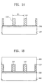
- FIGS. 1A through 1H are cross-sectional views illustrating a method of forming a fine pattern according to an embodiment of the technology.
- FIGS. 2A through 2H are cross-sectional views illustrating a method of forming a fine pattern according to another embodiment of the technology.
- FIGS. 1A through 1H are cross-sectional views illustrating a method of forming a fine pattern according to an embodiment of the technology.
- a pad layer 102 is formed on a substrate 100 .
- the substrate 100 includes a semiconductor substrate such as a silicon wafer or silicon on insulator (SOI) wafer. Structures such as an isolation layer, transistors and/or an interlayer dielectric layer can be additionally formed in the substrate 100 .
- the structures can be combined to form volatile memory devices or nonvolatile memory devices. However, descriptions of the structures will be omitted for brief description.
- the pad layer 102 includes at least one of a thermal oxidation layer and a silicon nitride layer.
- a first mask layer is formed on a surface of the pad layer 102 .
- the first mask layer includes a material layer having an etch selectivity with respect to the substrate 100 , in one embodiment, a silicon nitride layer.
- Photoresist patterns are formed on the first mask layer using a photolithography process such that they are spaced apart from one another at a predetermined distance. As viewed on a plan view, the photoresist patterns can be formed in a line type, a hole type and/or a combination type thereof.
- the first mask layer is etched using the photoresist patterns as an etching mask, thereby forming first mask patterns 110 spaced apart from one another at a predetermined distance.
- a distance between the first mask patterns 110 spaced apart from one another i.e., a first pitch size P 1 , can be substantially identical to limiting resolution of the photolithography process.
- a reaction promoting layer 112 is formed on the substrate 100 having the first mask patterns 110 .
- the reaction promoting layer 112 is formed to cover the substrate 100 and sidewalls and top surfaces of the first mask patterns 110 .
- the reaction promoting layer 112 can include a material layer containing hexamethyldisilazane (HMDS).
- HMDS-containing layer can be formed by supplying HMDS gas on the substrate 100 .
- a reactive layer 120 is formed on the surface of the substrate 100 having the reaction promoting layer 112 .
- the reactive layer 120 can include a polymer, a crosslinker and a surfactant, used in a crosslinking reaction.
- the reactive layer 120 can be formed using a spin coating process.
- the polymer is a material layer having an etch selectivity with respect to the first mask patterns 110 .
- the polymer can comprise a silicon oxide polymer having the following Chemical Formula 1:
- n denotes a positive number from 1 to 5000.
- At least one group comprising alkoxy and methoxy groups can be further included in the link site of the silicon oxide polymer. Therefore, the crosslinking reaction can be more actively produced.
- the crosslinker is interposed between the polymers to effectively produce the crosslinking reaction of the polymers.
- the crosslinker can comprise a material having the following Chemical Formula 2:
- R denotes an alkyl group
- n denotes a positive number from 1 to 5000.
- the surfactant can improve gapfill and coating properties of the silicon oxide polymer.
- a nonionic surfactant can be used as the surfactant.
- the reactive layer 120 including the silicon oxide polymer can be formed on the substrate 100 using the spin coating process. Gaps are formed between the first mask patterns 110 .
- a sacrificial layer 120 a is formed along outer walls of the first mask patterns 110 and the substrate 100 .
- the layer 120 a can be exposed between the first mask patterns 110 on the reaction promoting layer 112 using a chemical attachment process.
- a region in which the chemical attachment process is not performed in the reactive layer 120 remains as a non-reactive layer 120 b.
- the chemical attachment process can be performed employing a heating process 10 with respect to the substrate 100 .
- the heating process 10 is performed through a rear surface of the substrate 100 .
- the chemical attachment process can be performed while accompanying a crosslinking reaction performed at a boundary region between the reactive layer 120 and the reaction promoting layer 112 and a crosslinking reaction performed in the reactive layer 120 adjacent to the boundary region.
- the silicon nitride layer can have a small number of link sites capable of performing the crosslinking reaction.
- the crosslinking reaction of the HDMS layer can be easily performed with the reactive layer 120 .
- the crosslinking reaction in the silicon oxide polymers can also be produced in the reactive layer 120 adjacent to the first mask patterns 110 .
- the sacrificial layer 120 a is formed to have a uniform thickness on a surface of the reaction promoting layer 112 by adjusting the time and temperature of the heating process 10 .
- the sacrificial layer 120 a formed between sidewalls of the first mask patterns 110 facing each other is formed having grooves 122 .
- the grooves 122 are formed having a predetermined width under the control of the heating process 10 .
- the grooves 122 are formed to have a width W 1 substantially identical to the width W 2 of the first mask patterns 110 .
- the heating process 10 is performed at a temperature of about 100° C. to 120° C. for about 60 seconds to 90 seconds.
- the sacrificial layer 120 a is exposed by removing the non-reactive layer 120 b .
- the removal of the non-reactive layer 120 b can be accomplished by way of a removal process using a tetramethyl ammonium hydroxide (TMAH) solution 12 , or the like. Silicon oxide polymers contained in the non-reactive layer 120 b are dissolved by the TMAH solution 12 .
- the sacrificial layer 120 a in which the silicon oxide polymers are crosslinked with one another, is not dissolved by the TMAH solution 12 . That is, in the reactive layer 120 , the non-reactive layer 120 b is selectively dissolved in the TMAH solution 12 . Accordingly, the non-reactive layer 120 b is completely removed at boundaries of the grooves 122 , so that the grooves 122 can be exposed which have a substantially uniform width.
- TMAH tetramethyl ammonium hydroxide
- a second mask layer 130 is formed on the substrate 100 having the sacrificial layer 120 a .
- the second mask layer 130 includes a material layer having an etch selectivity with respect to the substrate 100 and the sacrificial layer 120 a .
- the second mask layer 130 can comprise the same material layer as the first mask patterns 110 .
- the second mask layer 130 is planarized such that it remains in the grooves 122 .
- second mask patterns 130 a are formed to fill the grooves 122 .
- the planarization process can be performed using an etchback or chemical mechanical polishing (CMP) technique.
- the second mask patterns 130 a can be formed to have a level substantially identical to top surfaces of the first mask patterns 110 using the etchback technique.
- the second mask patterns 130 a may be planarized to have a level substantially identical to a top surface of the sacrificial layer 120 a , so that the second mask patterns 130 are formed to have a higher level than the first mask patterns 110 .
- the second mask patterns 130 a are self-aligned through the grooves 122 . Accordingly, the first and second mask patterns 110 and 130 a are formed at a uniform distance, so that a precise patterning process can be performed.
- the sacrificial layer 120 a , the reaction promoting layer 112 formed beneath the sacrificial layer 120 a and the pad layer 102 are sequentially etched and removed, thereby exposing the first and second mask patterns 110 and 130 a and the substrate 100 between the first and second mask patterns 110 and 130 a .
- the sacrificial layer 120 a includes silicon oxide, it can be removed using an etching process employing CF 4 gas as an etching gas. In this case, the sacrificial layer 120 a may remain beneath the second mask patterns 130 a , and the pad layer 102 may remain beneath the first mask patterns 110 and the sacrificial layer 120 a.
- a distance between the first and second mask patterns 110 and 130 a is smaller than the first pitch size P 1 .
- an exposure apparatus having the first pitch size P 1 is provided with a light source having a wavelength relatively greater than an exposure apparatus capable of simultaneously forming the first and second mask patterns 110 and 130 a
- mask patterns having a smaller pitch size than the first pitch size P 1 can be formed through the aforementioned exposure apparatus having the first pitch size P 1 . That is, the mask patterns can be formed to have a smaller pitch size than the resolution of the photolithography process.
- the substrate 100 is etched using the first and second mask patterns 110 and 130 a as an etching mask, thereby forming trenches 140 defining active regions 142 .
- the etching of the substrate 100 can be performed using an anisotropic etching process, an isotropic etching process, or a combination process thereof.
- FIGS. 2A through 2H are cross-sectional views illustrating a method of forming a fine pattern according to another embodiment of the technology.
- first and second layers 204 and 206 are sequentially formed on a substrate 200 .
- the substrate 200 includes a semiconductor substrate such as a silicon wafer or SOI wafer. Structures such as a isolation layer, transistors and/or an interlayer dielectric layer can be additionally formed in the substrate 200 .
- the structures can be combined to form volatile memory devices or nonvolatile memory devices. However, descriptions of the structures will be omitted for brief description. Hereinafter, differences between the current embodiment and the embodiment described with reference to FIGS. 1A through 1H will be described in detail.
- the first layer 204 can include an insulating layer, a conductive layer, or a combination layer thereof.
- the second layer 206 can include a material layer different from the first layer 204 .
- the second layer 206 can also include an insulating layer, a conductive layer, or a combination layer thereof.
- the first layer 204 includes an interlayer dielectric layer
- the second layer 206 includes a conductive layer.
- the second layer 206 includes a poly-silicon layer.
- a buffer mask layer 208 is formed on the second layer 206 .
- the buffer mask layer 208 is formed of a material layer having an etch selectivity with respect to the second layer 206 , e.g., a silicon oxide layer.
- first mask patterns 210 spaced apart from one another at a predetermined distance are formed on the buffer mask layer 208 .
- a distance between the first mask patterns 210 spaced apart from one another, i.e., a pitch size can be substantially identical to resolution of the photolithography process.
- the first mask patterns 210 include silicon nitride layers or poly-silicon layers.
- a reactive layer 220 is formed on substantially the entire surface of the substrate 200 having the first mask patterns 210 .
- the reactive layer 220 can include a polymer, a crosslinker and a surfactant, used in a crosslinking reaction.
- the reactive layer 220 can be formed using a spin coating process.
- the polymer is a material layer having an etch selectivity with respect to the first mask patterns 210 .
- the polymer contains a silicon oxide polymer expressed by the aforementioned Chemical Formula 1. At least one group comprising alkoxy and/or methoxy groups can be in the link site of the silicon oxide polymer.
- the crosslinker is interposed between the polymers to effectively produce the crosslinking reaction of the polymers.
- the crosslinker can comprise a material expressed by the aforementioned Chemical Formula 2.
- a nonionic surfactant can be used as the surfactant.
- the second layer 206 can include a poly-silicon layer as described in the current embodiment
- the buffer mask layer 208 including a silicon oxide layer can be formed, so that the first mask patterns 210 can include poly-silicon layers.
- the poly-silicon layer can have link sites more than the silicon nitride layer. Accordingly, the reaction promoting layer 112 described with reference to FIG. 1B can be omitted.
- sacrificial layers 220 a can be formed along outer walls of the first mask patterns 210 on the substrate 200 using a chemical attachment process.
- a region at which the chemical attachment process is not performed in the reactive layer 220 remains as a non-react live layer 220 b.
- the chemical attachment process can be performed using a heating process 20 with respect to the substrate 200 , and the heating process 20 can be performed through a rear surface of the substrate 200 .
- the chemical attachment process can be performed while accompanying a crosslinking reaction performed at a boundary region between the reactive layer 220 and the first mask patterns 210 and a crosslinking reaction performed in the reactive layer 220 adjacent to the boundary region.
- the crosslinking reaction of the poly-silicon layers of the first mask patterns 210 can be performed with the reactive layer 220 .
- the crosslinking reaction between the silicon oxide polymer can also be produced in the reactive layer 220 adjacent to the first mask patterns 210 .
- the sacrificial layers 220 a may not be formed on the silicon oxide layer of the buffer mask layer 208 .
- the sacrificial layers 220 a are formed to have a substantially uniform thickness along the outer walls of the first mask patterns 210 by adjusting the time and temperature of the heating process 20 . Gaps between sidewalls of the sacrificial layers 220 a facing each other can be formed to have a predetermined width under the control of the heating process 20 . In this case, the width W 3 of the gaps between the sacrificial layers 220 a can be substantially identical to the width W 4 of the first mask patterns 210 .
- the heating process 20 is performed at a temperature of about 100° C. to 120° C. for about 60 to 90 seconds.
- the sacrificial layers 220 a are exposed by removing the non-reactive layer 220 b .
- the removal of the non-reactive layer 220 b includes a process of using a tetramethyl ammonium hydroxide (TMAH) solution 22 , or the like.
- TMAH tetramethyl ammonium hydroxide
- the non-reactive layer 220 b is selectively dissolved in the TMAH solution 22 . Accordingly, the non-reactive layer 220 b between the sacrificial layers 220 a is substantially completely removed, so that the sacrificial layers 220 a remaining has a substantially uniform width.
- a second mask layer 230 is formed on the substrate 200 having the sacrificial layers 220 a .
- the second mask layer 230 can include the same material layer as the first mask patterns 210 .
- the second mask layer 230 is planarized such that it remains in the gaps between the sacrificial layers 220 a .
- second mask patterns 230 a are formed to fill the gaps.
- a planarization process can be performed using an etchback or chemical mechanical polishing (CMP) technique.
- the second mask patterns 230 a can be formed to have a level substantially identical to top surfaces of the first mask patterns 210 using the etchback technique.
- the second mask patterns 230 a are self-aligned through the gaps.
- the sacrificial layers 220 a and the buffer mask layer 208 between the first and second mask patterns 210 and 230 a are sequentially etched and removed, thereby exposing the first and second mask patterns 210 and 230 a and the substrate 200 between the first and second mask patterns 210 and 230 a .
- the sacrificial layers 220 a include silicon oxides, they can be removed using an etching process employing CF 4 gas as an etching gas. In this case, buffer mask patterns 208 a may remain beneath the first and second mask patterns 210 and 230 a.
- an exposure apparatus having a great pitch size such as a distance between the first mask patterns 210 is provided with a light source having a wavelength relatively greater than an exposure apparatus capable of simultaneously forming the first and second mask patterns 210 and 230 a
- mask patterns having a smaller pitch size than the pitch size can be formed through the aforementioned exposure apparatus having a great pitch size. That is, the mask patterns can be formed to have a smaller pitch size than the limiting resolution of the photolithography process.
- the second layer 206 is etched using the first and second mask patterns 210 and 230 a and the buffer mask patterns 208 a as an etching mask, thereby forming conductive patterns 206 a .
- the etching of the second layer 206 can be performed using an anisotropic etching process, an isotropic etching process, or a process employing the both.
- the first and second mask patterns 210 and 230 a include poly-silicon layers, the first and second mask patterns 210 and 230 a may be reduced.
- the buffer mask pattern 208 a since the buffer mask pattern 208 a has etching resistance, the buffer mask pattern 208 a can serve as an etching mask while the second layer 206 is etched.
- the first and second mask patterns 210 and 230 a may be formed to expose a predetermined region of the interlayer dielectric layer.
- the first and second mask patterns 210 and 230 a may be formed using the method described with reference to the aforementioned embodiment.
- second mask patterns are formed between sacrificial layers formed along outer walls of the first mask patterns, so that the first and second mask patterns can be formed to have a smaller pitch size than limiting resolution of a photolithography process.
- a crosslinking reaction of a reactive layer is performed with the first mask patterns around the first mask patterns, thereby forming the sacrificial layers.
- the sacrificial layers can be controlled to have a uniform width along the outer walls of the first mask patterns. Accordingly, the sacrificial layers can be formed to have uniform gaps between the first mask patterns.
Landscapes
- Engineering & Computer Science (AREA)
- Manufacturing & Machinery (AREA)
- Physics & Mathematics (AREA)
- Condensed Matter Physics & Semiconductors (AREA)
- General Physics & Mathematics (AREA)
- Computer Hardware Design (AREA)
- Microelectronics & Electronic Packaging (AREA)
- Power Engineering (AREA)
- Inorganic Chemistry (AREA)
- Chemical & Material Sciences (AREA)
- Internal Circuitry In Semiconductor Integrated Circuit Devices (AREA)
- Photosensitive Polymer And Photoresist Processing (AREA)
- Exposure Of Semiconductors, Excluding Electron Or Ion Beam Exposure (AREA)
Applications Claiming Priority (3)
| Application Number | Priority Date | Filing Date | Title |
|---|---|---|---|
| KR2007-0055456 | 2007-06-07 | ||
| KR10-2007-0055456 | 2007-06-07 | ||
| KR1020070055456A KR100886219B1 (ko) | 2007-06-07 | 2007-06-07 | 자기정렬된 이중 패터닝을 채택하는 미세 패턴 형성 방법 |
Publications (2)
| Publication Number | Publication Date |
|---|---|
| US20080305636A1 US20080305636A1 (en) | 2008-12-11 |
| US8071484B2 true US8071484B2 (en) | 2011-12-06 |
Family
ID=40096275
Family Applications (1)
| Application Number | Title | Priority Date | Filing Date |
|---|---|---|---|
| US12/132,548 Expired - Fee Related US8071484B2 (en) | 2007-06-07 | 2008-06-03 | Method of forming fine pattern employing self-aligned double patterning |
Country Status (3)
| Country | Link |
|---|---|
| US (1) | US8071484B2 (ko) |
| JP (1) | JP5143635B2 (ko) |
| KR (1) | KR100886219B1 (ko) |
Cited By (6)
| Publication number | Priority date | Publication date | Assignee | Title |
|---|---|---|---|---|
| US20120043646A1 (en) * | 2010-08-20 | 2012-02-23 | Globalfoundries Inc. | Spacer double patterning that prints multiple cd in front-end-of-line |
| US20120248442A1 (en) * | 2011-04-04 | 2012-10-04 | Se-Hwan Yu | Method of forming a fine pattern, display substrate, and method of manufacturing the same using the method of forming a fine pattern |
| US20130065326A1 (en) * | 2011-09-09 | 2013-03-14 | Gaku Sudo | Method for manufacturing semiconductor device |
| US20150380209A1 (en) * | 2014-06-30 | 2015-12-31 | Taiwan Semiconductor Manufacturing Co., Ltd | Dimension measurement apparatus calibration standard and method for forming the same |
| US10032638B2 (en) | 2015-05-19 | 2018-07-24 | Samsung Electronics Co., Ltd. | Method of fabricating pattern structure |
| US10062571B2 (en) | 2016-01-26 | 2018-08-28 | Samsung Electronics Co., Ltd. | Method of manufacturing semiconductor device |
Families Citing this family (30)
| Publication number | Priority date | Publication date | Assignee | Title |
|---|---|---|---|---|
| US8852851B2 (en) | 2006-07-10 | 2014-10-07 | Micron Technology, Inc. | Pitch reduction technology using alternating spacer depositions during the formation of a semiconductor device and systems including same |
| US7989307B2 (en) | 2008-05-05 | 2011-08-02 | Micron Technology, Inc. | Methods of forming isolated active areas, trenches, and conductive lines in semiconductor structures and semiconductor structures including the same |
| US10151981B2 (en) * | 2008-05-22 | 2018-12-11 | Micron Technology, Inc. | Methods of forming structures supported by semiconductor substrates |
| US8247302B2 (en) | 2008-12-04 | 2012-08-21 | Micron Technology, Inc. | Methods of fabricating substrates |
| US8796155B2 (en) * | 2008-12-04 | 2014-08-05 | Micron Technology, Inc. | Methods of fabricating substrates |
| US8273634B2 (en) | 2008-12-04 | 2012-09-25 | Micron Technology, Inc. | Methods of fabricating substrates |
| KR101045371B1 (ko) * | 2008-12-22 | 2011-06-30 | 주식회사 하이닉스반도체 | 이중 패터닝을 이용한 미세 패턴 형성 방법 |
| US8268543B2 (en) * | 2009-03-23 | 2012-09-18 | Micron Technology, Inc. | Methods of forming patterns on substrates |
| US9330934B2 (en) | 2009-05-18 | 2016-05-03 | Micron Technology, Inc. | Methods of forming patterns on substrates |
| US8518788B2 (en) | 2010-08-11 | 2013-08-27 | Micron Technology, Inc. | Methods of forming a plurality of capacitors |
| US8455341B2 (en) | 2010-09-02 | 2013-06-04 | Micron Technology, Inc. | Methods of forming features of integrated circuitry |
| JP5821100B2 (ja) | 2010-12-17 | 2015-11-24 | カール ツァイス エスエムエス ゲーエムベーハー | フォトリソグラフィマスクによって処理されるウェーハ上の誤差を補正する方法及び装置 |
| US8575032B2 (en) | 2011-05-05 | 2013-11-05 | Micron Technology, Inc. | Methods of forming a pattern on a substrate |
| US9076680B2 (en) | 2011-10-18 | 2015-07-07 | Micron Technology, Inc. | Integrated circuitry, methods of forming capacitors, and methods of forming integrated circuitry comprising an array of capacitors and circuitry peripheral to the array |
| US9177794B2 (en) | 2012-01-13 | 2015-11-03 | Micron Technology, Inc. | Methods of patterning substrates |
| US8629048B1 (en) | 2012-07-06 | 2014-01-14 | Micron Technology, Inc. | Methods of forming a pattern on a substrate |
| CN103794475B (zh) * | 2012-10-30 | 2016-10-05 | 中芯国际集成电路制造(上海)有限公司 | 自对准三重图形化方法 |
| US8835328B2 (en) * | 2013-02-08 | 2014-09-16 | GlobalFoundries, Inc. | Methods for fabricating integrated circuits with improved semiconductor fin structures |
| JP6026375B2 (ja) | 2013-09-02 | 2016-11-16 | 株式会社東芝 | 半導体装置の製造方法 |
| US9564361B2 (en) * | 2013-09-13 | 2017-02-07 | Qualcomm Incorporated | Reverse self aligned double patterning process for back end of line fabrication of a semiconductor device |
| CN103943468A (zh) * | 2014-05-08 | 2014-07-23 | 上海华力微电子有限公司 | 一种图形自对准形成方法 |
| CN105336571B (zh) * | 2014-07-28 | 2018-06-01 | 中芯国际集成电路制造(上海)有限公司 | 自对准多重图形掩膜的形成方法 |
| US9991132B2 (en) * | 2015-04-17 | 2018-06-05 | Taiwan Semiconductor Manufacturing Company, Ltd. | Lithographic technique incorporating varied pattern materials |
| US9455177B1 (en) * | 2015-08-31 | 2016-09-27 | Dow Global Technologies Llc | Contact hole formation methods |
| US10211051B2 (en) * | 2015-11-13 | 2019-02-19 | Canon Kabushiki Kaisha | Method of reverse tone patterning |
| JP6213610B2 (ja) * | 2016-04-27 | 2017-10-18 | 大日本印刷株式会社 | ナノインプリントリソグラフィ用テンプレートの製造方法 |
| US9685440B1 (en) * | 2016-06-29 | 2017-06-20 | International Business Machines Corporation | Forming fins utilizing alternating pattern of spacers |
| US10115594B1 (en) * | 2017-09-05 | 2018-10-30 | Nanya Technology Corporation | Method of forming fine island patterns of semiconductor devices |
| US10475648B1 (en) | 2018-05-01 | 2019-11-12 | United Microelectronics Corp. | Method for patterning a semiconductor structure |
| CN113013076B (zh) * | 2021-02-25 | 2022-06-10 | 长鑫存储技术有限公司 | 套刻标记的形成方法及半导体结构 |
Citations (12)
| Publication number | Priority date | Publication date | Assignee | Title |
|---|---|---|---|---|
| US5686223A (en) | 1994-12-22 | 1997-11-11 | Cypress Semiconductor Corp. | Method for reduced pitch lithography |
| JPH1073927A (ja) | 1996-07-05 | 1998-03-17 | Mitsubishi Electric Corp | 微細パターン形成材料及びこれを用いた半導体装置の製造方法並びに半導体装置 |
| US6319853B1 (en) * | 1998-01-09 | 2001-11-20 | Mitsubishi Denki Kabushiki Kaisha | Method of manufacturing a semiconductor device using a minute resist pattern, and a semiconductor device manufactured thereby |
| US6833326B2 (en) * | 2002-03-26 | 2004-12-21 | Hynix Semiconductor Inc. | Method for forming fine patterns in semiconductor device |
| US20060079628A1 (en) * | 2002-06-24 | 2006-04-13 | Yoshiki Sugeta | Over-coating agent for forming fine patterns and a method of forming fine patterns using such agent |
| KR100574999B1 (ko) * | 2004-12-06 | 2006-04-28 | 삼성전자주식회사 | 반도체소자의 패턴 형성방법 |
| US20060160028A1 (en) * | 2005-01-17 | 2006-07-20 | Hyung-Rae Lee | Method of forming fine patterns of a semiconductor device |
| KR20060100251A (ko) | 2005-03-16 | 2006-09-20 | 가부시끼가이샤 도시바 | 패턴 형성 방법 및 반도체 장치의 제조 방법 |
| KR20060110097A (ko) | 2005-04-19 | 2006-10-24 | 삼성전자주식회사 | 미세 피치의 하드마스크를 이용한 반도체 소자의 미세 패턴형성 방법 |
| KR20060110706A (ko) | 2005-04-21 | 2006-10-25 | 삼성전자주식회사 | 이중 스페이서들을 이용한 미세 피치의 패턴 형성 방법 |
| KR20060134234A (ko) | 2005-06-22 | 2006-12-28 | 삼성전자주식회사 | 미세 패턴 형성 방법 |
| US7855154B2 (en) * | 2003-05-12 | 2010-12-21 | Micron Technology, Inc. | Methods of forming intermediate semiconductor device structures using spin-on, photopatternable, interlayer dielectric materials |
-
2007
- 2007-06-07 KR KR1020070055456A patent/KR100886219B1/ko not_active IP Right Cessation
-
2008
- 2008-06-03 US US12/132,548 patent/US8071484B2/en not_active Expired - Fee Related
- 2008-06-09 JP JP2008151118A patent/JP5143635B2/ja not_active Expired - Fee Related
Patent Citations (13)
| Publication number | Priority date | Publication date | Assignee | Title |
|---|---|---|---|---|
| US5686223A (en) | 1994-12-22 | 1997-11-11 | Cypress Semiconductor Corp. | Method for reduced pitch lithography |
| JPH1073927A (ja) | 1996-07-05 | 1998-03-17 | Mitsubishi Electric Corp | 微細パターン形成材料及びこれを用いた半導体装置の製造方法並びに半導体装置 |
| US6319853B1 (en) * | 1998-01-09 | 2001-11-20 | Mitsubishi Denki Kabushiki Kaisha | Method of manufacturing a semiconductor device using a minute resist pattern, and a semiconductor device manufactured thereby |
| US6833326B2 (en) * | 2002-03-26 | 2004-12-21 | Hynix Semiconductor Inc. | Method for forming fine patterns in semiconductor device |
| US20060079628A1 (en) * | 2002-06-24 | 2006-04-13 | Yoshiki Sugeta | Over-coating agent for forming fine patterns and a method of forming fine patterns using such agent |
| US7855154B2 (en) * | 2003-05-12 | 2010-12-21 | Micron Technology, Inc. | Methods of forming intermediate semiconductor device structures using spin-on, photopatternable, interlayer dielectric materials |
| KR100574999B1 (ko) * | 2004-12-06 | 2006-04-28 | 삼성전자주식회사 | 반도체소자의 패턴 형성방법 |
| US20060160028A1 (en) * | 2005-01-17 | 2006-07-20 | Hyung-Rae Lee | Method of forming fine patterns of a semiconductor device |
| JP2006261307A (ja) | 2005-03-16 | 2006-09-28 | Toshiba Corp | パターン形成方法 |
| KR20060100251A (ko) | 2005-03-16 | 2006-09-20 | 가부시끼가이샤 도시바 | 패턴 형성 방법 및 반도체 장치의 제조 방법 |
| KR20060110097A (ko) | 2005-04-19 | 2006-10-24 | 삼성전자주식회사 | 미세 피치의 하드마스크를 이용한 반도체 소자의 미세 패턴형성 방법 |
| KR20060110706A (ko) | 2005-04-21 | 2006-10-25 | 삼성전자주식회사 | 이중 스페이서들을 이용한 미세 피치의 패턴 형성 방법 |
| KR20060134234A (ko) | 2005-06-22 | 2006-12-28 | 삼성전자주식회사 | 미세 패턴 형성 방법 |
Cited By (11)
| Publication number | Priority date | Publication date | Assignee | Title |
|---|---|---|---|---|
| US20120043646A1 (en) * | 2010-08-20 | 2012-02-23 | Globalfoundries Inc. | Spacer double patterning that prints multiple cd in front-end-of-line |
| US8450833B2 (en) * | 2010-08-20 | 2013-05-28 | Globalfoundries Inc. | Spacer double patterning that prints multiple CD in front-end-of-line |
| US20120248442A1 (en) * | 2011-04-04 | 2012-10-04 | Se-Hwan Yu | Method of forming a fine pattern, display substrate, and method of manufacturing the same using the method of forming a fine pattern |
| US8575031B2 (en) * | 2011-04-04 | 2013-11-05 | Samsung Display Co., Ltd. | Method of forming a fine pattern, display substrate, and method of manufacturing the same using the method of forming a fine pattern |
| US20130065326A1 (en) * | 2011-09-09 | 2013-03-14 | Gaku Sudo | Method for manufacturing semiconductor device |
| US8835268B2 (en) * | 2011-09-09 | 2014-09-16 | Kabushiki Kaisha Toshiba | Method for manufacturing semiconductor device |
| US20150380209A1 (en) * | 2014-06-30 | 2015-12-31 | Taiwan Semiconductor Manufacturing Co., Ltd | Dimension measurement apparatus calibration standard and method for forming the same |
| US9691587B2 (en) * | 2014-06-30 | 2017-06-27 | Taiwan Semiconductor Manufacturing Co., Ltd. | Dimension measurement apparatus calibration standard and method for forming the same |
| US10032638B2 (en) | 2015-05-19 | 2018-07-24 | Samsung Electronics Co., Ltd. | Method of fabricating pattern structure |
| US10854465B2 (en) | 2015-05-19 | 2020-12-01 | Samsung Electronics Co., Ltd. | Method of fabricating pattern structure |
| US10062571B2 (en) | 2016-01-26 | 2018-08-28 | Samsung Electronics Co., Ltd. | Method of manufacturing semiconductor device |
Also Published As
| Publication number | Publication date |
|---|---|
| JP2008304923A (ja) | 2008-12-18 |
| JP5143635B2 (ja) | 2013-02-13 |
| US20080305636A1 (en) | 2008-12-11 |
| KR100886219B1 (ko) | 2009-02-27 |
| KR20080107557A (ko) | 2008-12-11 |
Similar Documents
| Publication | Publication Date | Title |
|---|---|---|
| US8071484B2 (en) | Method of forming fine pattern employing self-aligned double patterning | |
| US7754622B2 (en) | Patterning method utilizing SiBN and photolithography | |
| US7354847B2 (en) | Method of trimming technology | |
| US7709275B2 (en) | Method of forming a pattern for a semiconductor device and method of forming the related MOS transistor | |
| US8138093B2 (en) | Method for forming trenches having different widths and the same depth | |
| US8951918B2 (en) | Method for fabricating patterned structure of semiconductor device | |
| JP5001109B2 (ja) | 半導体素子の微細パターン形成方法 | |
| US20160307769A1 (en) | Lithographic Technique Incorporating Varied Pattern Materials | |
| US9188883B2 (en) | Alignment mark | |
| JP2009158907A (ja) | 半導体素子の微細パターン形成方法 | |
| US20050106837A1 (en) | Method for manufacturing a semiconductor device | |
| US10892184B2 (en) | Photobucket floor colors with selective grafting | |
| US20070010053A1 (en) | Method for fabricating conductive line | |
| KR20090097151A (ko) | 혼합형 광학 및 전자 빔 리소그래피 가공 레벨의 상호정렬 방법, 집적 회로 칩 제조 방법 및 집적 회로 구조체 | |
| US20110076832A1 (en) | Dual etch method of defining active area in semiconductor device | |
| KR101056060B1 (ko) | 수직 트랜지스터의 자기 정렬 컨택 형성방법 및 컨택홀을 포함하는 수직 트랜지스터 | |
| JPWO2009054413A1 (ja) | 半導体装置の作製方法 | |
| KR100741926B1 (ko) | 폴리실리콘 패턴 형성 방법 | |
| US20080122019A1 (en) | Semiconductor Device and Method of Manufacturing the Same | |
| US7563690B2 (en) | Method for forming shallow trench isolation region | |
| US7015148B1 (en) | Reduce line end pull back by exposing and etching space after mask one trim and etch | |
| US20080020569A1 (en) | Method for Manufacturing Semiconductor Device | |
| US7071085B1 (en) | Predefined critical spaces in IC patterning to reduce line end pull back | |
| KR100939168B1 (ko) | 반도체 소자의 패턴 형성 방법 | |
| US7867834B2 (en) | Manufacturing method of semiconductor device capable of forming the line width of a gate |
Legal Events
| Date | Code | Title | Description |
|---|---|---|---|
| AS | Assignment |
Owner name: SAMSUNG ELECTRONICS CO., LTD., KOREA, REPUBLIC OF Free format text: ASSIGNMENT OF ASSIGNORS INTEREST;ASSIGNORS:KIM, KYOUNG-MI;KIM, JAE-HO;KIM, YOUNG-HO;AND OTHERS;REEL/FRAME:021035/0608 Effective date: 20080502 |
|
| REMI | Maintenance fee reminder mailed | ||
| LAPS | Lapse for failure to pay maintenance fees | ||
| STCH | Information on status: patent discontinuation |
Free format text: PATENT EXPIRED DUE TO NONPAYMENT OF MAINTENANCE FEES UNDER 37 CFR 1.362 |
|
| FP | Lapsed due to failure to pay maintenance fee |
Effective date: 20151206 |