US6787451B2 - Semiconductor device and manufacturing method thereof - Google Patents
Semiconductor device and manufacturing method thereof Download PDFInfo
- Publication number
- US6787451B2 US6787451B2 US10/216,792 US21679202A US6787451B2 US 6787451 B2 US6787451 B2 US 6787451B2 US 21679202 A US21679202 A US 21679202A US 6787451 B2 US6787451 B2 US 6787451B2
- Authority
- US
- United States
- Prior art keywords
- film
- heat treatment
- forming
- sio
- boundary
- Prior art date
- Legal status (The legal status is an assumption and is not a legal conclusion. Google has not performed a legal analysis and makes no representation as to the accuracy of the status listed.)
- Expired - Lifetime
Links
Images


Classifications
-
- H—ELECTRICITY
- H10—SEMICONDUCTOR DEVICES; ELECTRIC SOLID-STATE DEVICES NOT OTHERWISE PROVIDED FOR
- H10D—INORGANIC ELECTRIC SEMICONDUCTOR DEVICES
- H10D64/00—Electrodes of devices having potential barriers
- H10D64/60—Electrodes characterised by their materials
- H10D64/66—Electrodes having a conductor capacitively coupled to a semiconductor by an insulator, e.g. MIS electrodes
- H10D64/671—Electrodes having a conductor capacitively coupled to a semiconductor by an insulator, e.g. MIS electrodes the conductor having lateral variation in doping or structure
-
- H—ELECTRICITY
- H01—ELECTRIC ELEMENTS
- H01L—SEMICONDUCTOR DEVICES NOT COVERED BY CLASS H10
- H01L21/00—Processes or apparatus adapted for the manufacture or treatment of semiconductor or solid state devices or of parts thereof
- H01L21/02—Manufacture or treatment of semiconductor devices or of parts thereof
- H01L21/02104—Forming layers
- H01L21/02107—Forming insulating materials on a substrate
- H01L21/02109—Forming insulating materials on a substrate characterised by the type of layer, e.g. type of material, porous/non-porous, pre-cursors, mixtures or laminates
- H01L21/02112—Forming insulating materials on a substrate characterised by the type of layer, e.g. type of material, porous/non-porous, pre-cursors, mixtures or laminates characterised by the material of the layer
- H01L21/02123—Forming insulating materials on a substrate characterised by the type of layer, e.g. type of material, porous/non-porous, pre-cursors, mixtures or laminates characterised by the material of the layer the material containing silicon
- H01L21/02126—Forming insulating materials on a substrate characterised by the type of layer, e.g. type of material, porous/non-porous, pre-cursors, mixtures or laminates characterised by the material of the layer the material containing silicon the material containing Si, O, and at least one of H, N, C, F, or other non-metal elements, e.g. SiOC, SiOC:H or SiONC
- H01L21/0214—Forming insulating materials on a substrate characterised by the type of layer, e.g. type of material, porous/non-porous, pre-cursors, mixtures or laminates characterised by the material of the layer the material containing silicon the material containing Si, O, and at least one of H, N, C, F, or other non-metal elements, e.g. SiOC, SiOC:H or SiONC the material being a silicon oxynitride, e.g. SiON or SiON:H
-
- H—ELECTRICITY
- H01—ELECTRIC ELEMENTS
- H01L—SEMICONDUCTOR DEVICES NOT COVERED BY CLASS H10
- H01L21/00—Processes or apparatus adapted for the manufacture or treatment of semiconductor or solid state devices or of parts thereof
- H01L21/02—Manufacture or treatment of semiconductor devices or of parts thereof
- H01L21/02104—Forming layers
- H01L21/02107—Forming insulating materials on a substrate
- H01L21/02109—Forming insulating materials on a substrate characterised by the type of layer, e.g. type of material, porous/non-porous, pre-cursors, mixtures or laminates
- H01L21/02112—Forming insulating materials on a substrate characterised by the type of layer, e.g. type of material, porous/non-porous, pre-cursors, mixtures or laminates characterised by the material of the layer
- H01L21/02123—Forming insulating materials on a substrate characterised by the type of layer, e.g. type of material, porous/non-porous, pre-cursors, mixtures or laminates characterised by the material of the layer the material containing silicon
- H01L21/02164—Forming insulating materials on a substrate characterised by the type of layer, e.g. type of material, porous/non-porous, pre-cursors, mixtures or laminates characterised by the material of the layer the material containing silicon the material being a silicon oxide, e.g. SiO2
-
- H—ELECTRICITY
- H01—ELECTRIC ELEMENTS
- H01L—SEMICONDUCTOR DEVICES NOT COVERED BY CLASS H10
- H01L21/00—Processes or apparatus adapted for the manufacture or treatment of semiconductor or solid state devices or of parts thereof
- H01L21/02—Manufacture or treatment of semiconductor devices or of parts thereof
- H01L21/02104—Forming layers
- H01L21/02107—Forming insulating materials on a substrate
- H01L21/02109—Forming insulating materials on a substrate characterised by the type of layer, e.g. type of material, porous/non-porous, pre-cursors, mixtures or laminates
- H01L21/02112—Forming insulating materials on a substrate characterised by the type of layer, e.g. type of material, porous/non-porous, pre-cursors, mixtures or laminates characterised by the material of the layer
- H01L21/02172—Forming insulating materials on a substrate characterised by the type of layer, e.g. type of material, porous/non-porous, pre-cursors, mixtures or laminates characterised by the material of the layer the material containing at least one metal element, e.g. metal oxides, metal nitrides, metal oxynitrides or metal carbides
- H01L21/02175—Forming insulating materials on a substrate characterised by the type of layer, e.g. type of material, porous/non-porous, pre-cursors, mixtures or laminates characterised by the material of the layer the material containing at least one metal element, e.g. metal oxides, metal nitrides, metal oxynitrides or metal carbides characterised by the metal
- H01L21/02178—Forming insulating materials on a substrate characterised by the type of layer, e.g. type of material, porous/non-porous, pre-cursors, mixtures or laminates characterised by the material of the layer the material containing at least one metal element, e.g. metal oxides, metal nitrides, metal oxynitrides or metal carbides characterised by the metal the material containing aluminium, e.g. Al2O3
-
- H—ELECTRICITY
- H01—ELECTRIC ELEMENTS
- H01L—SEMICONDUCTOR DEVICES NOT COVERED BY CLASS H10
- H01L21/00—Processes or apparatus adapted for the manufacture or treatment of semiconductor or solid state devices or of parts thereof
- H01L21/02—Manufacture or treatment of semiconductor devices or of parts thereof
- H01L21/02104—Forming layers
- H01L21/02107—Forming insulating materials on a substrate
- H01L21/02225—Forming insulating materials on a substrate characterised by the process for the formation of the insulating layer
- H01L21/0226—Forming insulating materials on a substrate characterised by the process for the formation of the insulating layer formation by a deposition process
- H01L21/02263—Forming insulating materials on a substrate characterised by the process for the formation of the insulating layer formation by a deposition process deposition from the gas or vapour phase
- H01L21/02266—Forming insulating materials on a substrate characterised by the process for the formation of the insulating layer formation by a deposition process deposition from the gas or vapour phase deposition by physical ablation of a target, e.g. sputtering, reactive sputtering, physical vapour deposition or pulsed laser deposition
-
- H—ELECTRICITY
- H01—ELECTRIC ELEMENTS
- H01L—SEMICONDUCTOR DEVICES NOT COVERED BY CLASS H10
- H01L21/00—Processes or apparatus adapted for the manufacture or treatment of semiconductor or solid state devices or of parts thereof
- H01L21/02—Manufacture or treatment of semiconductor devices or of parts thereof
- H01L21/02104—Forming layers
- H01L21/02107—Forming insulating materials on a substrate
- H01L21/02296—Forming insulating materials on a substrate characterised by the treatment performed before or after the formation of the layer
- H01L21/02318—Forming insulating materials on a substrate characterised by the treatment performed before or after the formation of the layer post-treatment
- H01L21/02321—Forming insulating materials on a substrate characterised by the treatment performed before or after the formation of the layer post-treatment introduction of substances into an already existing insulating layer
- H01L21/02323—Forming insulating materials on a substrate characterised by the treatment performed before or after the formation of the layer post-treatment introduction of substances into an already existing insulating layer introduction of oxygen
-
- H—ELECTRICITY
- H01—ELECTRIC ELEMENTS
- H01L—SEMICONDUCTOR DEVICES NOT COVERED BY CLASS H10
- H01L21/00—Processes or apparatus adapted for the manufacture or treatment of semiconductor or solid state devices or of parts thereof
- H01L21/02—Manufacture or treatment of semiconductor devices or of parts thereof
- H01L21/02104—Forming layers
- H01L21/02107—Forming insulating materials on a substrate
- H01L21/02296—Forming insulating materials on a substrate characterised by the treatment performed before or after the formation of the layer
- H01L21/02318—Forming insulating materials on a substrate characterised by the treatment performed before or after the formation of the layer post-treatment
- H01L21/02321—Forming insulating materials on a substrate characterised by the treatment performed before or after the formation of the layer post-treatment introduction of substances into an already existing insulating layer
- H01L21/02329—Forming insulating materials on a substrate characterised by the treatment performed before or after the formation of the layer post-treatment introduction of substances into an already existing insulating layer introduction of nitrogen
-
- H—ELECTRICITY
- H01—ELECTRIC ELEMENTS
- H01L—SEMICONDUCTOR DEVICES NOT COVERED BY CLASS H10
- H01L21/00—Processes or apparatus adapted for the manufacture or treatment of semiconductor or solid state devices or of parts thereof
- H01L21/02—Manufacture or treatment of semiconductor devices or of parts thereof
- H01L21/02104—Forming layers
- H01L21/02107—Forming insulating materials on a substrate
- H01L21/02296—Forming insulating materials on a substrate characterised by the treatment performed before or after the formation of the layer
- H01L21/02318—Forming insulating materials on a substrate characterised by the treatment performed before or after the formation of the layer post-treatment
- H01L21/02337—Forming insulating materials on a substrate characterised by the treatment performed before or after the formation of the layer post-treatment treatment by exposure to a gas or vapour
-
- H—ELECTRICITY
- H01—ELECTRIC ELEMENTS
- H01L—SEMICONDUCTOR DEVICES NOT COVERED BY CLASS H10
- H01L21/00—Processes or apparatus adapted for the manufacture or treatment of semiconductor or solid state devices or of parts thereof
- H01L21/02—Manufacture or treatment of semiconductor devices or of parts thereof
- H01L21/04—Manufacture or treatment of semiconductor devices or of parts thereof the devices having potential barriers, e.g. a PN junction, depletion layer or carrier concentration layer
- H01L21/18—Manufacture or treatment of semiconductor devices or of parts thereof the devices having potential barriers, e.g. a PN junction, depletion layer or carrier concentration layer the devices having semiconductor bodies comprising elements of Group IV of the Periodic Table or AIIIBV compounds with or without impurities, e.g. doping materials
- H01L21/28—Manufacture of electrodes on semiconductor bodies using processes or apparatus not provided for in groups H01L21/20 - H01L21/268
- H01L21/28008—Making conductor-insulator-semiconductor electrodes
- H01L21/28017—Making conductor-insulator-semiconductor electrodes the insulator being formed after the semiconductor body, the semiconductor being silicon
- H01L21/28026—Making conductor-insulator-semiconductor electrodes the insulator being formed after the semiconductor body, the semiconductor being silicon characterised by the conductor
- H01L21/28035—Making conductor-insulator-semiconductor electrodes the insulator being formed after the semiconductor body, the semiconductor being silicon characterised by the conductor the final conductor layer next to the insulator being silicon, e.g. polysilicon, with or without impurities
- H01L21/28044—Making conductor-insulator-semiconductor electrodes the insulator being formed after the semiconductor body, the semiconductor being silicon characterised by the conductor the final conductor layer next to the insulator being silicon, e.g. polysilicon, with or without impurities the conductor comprising at least another non-silicon conductive layer
- H01L21/28061—Making conductor-insulator-semiconductor electrodes the insulator being formed after the semiconductor body, the semiconductor being silicon characterised by the conductor the final conductor layer next to the insulator being silicon, e.g. polysilicon, with or without impurities the conductor comprising at least another non-silicon conductive layer the conductor comprising a metal or metal silicide formed by deposition, e.g. sputter deposition, i.e. without a silicidation reaction
-
- H—ELECTRICITY
- H01—ELECTRIC ELEMENTS
- H01L—SEMICONDUCTOR DEVICES NOT COVERED BY CLASS H10
- H01L21/00—Processes or apparatus adapted for the manufacture or treatment of semiconductor or solid state devices or of parts thereof
- H01L21/02—Manufacture or treatment of semiconductor devices or of parts thereof
- H01L21/04—Manufacture or treatment of semiconductor devices or of parts thereof the devices having potential barriers, e.g. a PN junction, depletion layer or carrier concentration layer
- H01L21/18—Manufacture or treatment of semiconductor devices or of parts thereof the devices having potential barriers, e.g. a PN junction, depletion layer or carrier concentration layer the devices having semiconductor bodies comprising elements of Group IV of the Periodic Table or AIIIBV compounds with or without impurities, e.g. doping materials
- H01L21/28—Manufacture of electrodes on semiconductor bodies using processes or apparatus not provided for in groups H01L21/20 - H01L21/268
- H01L21/28008—Making conductor-insulator-semiconductor electrodes
- H01L21/28017—Making conductor-insulator-semiconductor electrodes the insulator being formed after the semiconductor body, the semiconductor being silicon
- H01L21/28158—Making the insulator
- H01L21/28167—Making the insulator on single crystalline silicon, e.g. using a liquid, i.e. chemical oxidation
- H01L21/28185—Making the insulator on single crystalline silicon, e.g. using a liquid, i.e. chemical oxidation with a treatment, e.g. annealing, after the formation of the gate insulator and before the formation of the definitive gate conductor
-
- H—ELECTRICITY
- H01—ELECTRIC ELEMENTS
- H01L—SEMICONDUCTOR DEVICES NOT COVERED BY CLASS H10
- H01L21/00—Processes or apparatus adapted for the manufacture or treatment of semiconductor or solid state devices or of parts thereof
- H01L21/02—Manufacture or treatment of semiconductor devices or of parts thereof
- H01L21/04—Manufacture or treatment of semiconductor devices or of parts thereof the devices having potential barriers, e.g. a PN junction, depletion layer or carrier concentration layer
- H01L21/18—Manufacture or treatment of semiconductor devices or of parts thereof the devices having potential barriers, e.g. a PN junction, depletion layer or carrier concentration layer the devices having semiconductor bodies comprising elements of Group IV of the Periodic Table or AIIIBV compounds with or without impurities, e.g. doping materials
- H01L21/28—Manufacture of electrodes on semiconductor bodies using processes or apparatus not provided for in groups H01L21/20 - H01L21/268
- H01L21/28008—Making conductor-insulator-semiconductor electrodes
- H01L21/28017—Making conductor-insulator-semiconductor electrodes the insulator being formed after the semiconductor body, the semiconductor being silicon
- H01L21/28158—Making the insulator
- H01L21/28167—Making the insulator on single crystalline silicon, e.g. using a liquid, i.e. chemical oxidation
- H01L21/28194—Making the insulator on single crystalline silicon, e.g. using a liquid, i.e. chemical oxidation by deposition, e.g. evaporation, ALD, CVD, sputtering, laser deposition
-
- H—ELECTRICITY
- H01—ELECTRIC ELEMENTS
- H01L—SEMICONDUCTOR DEVICES NOT COVERED BY CLASS H10
- H01L21/00—Processes or apparatus adapted for the manufacture or treatment of semiconductor or solid state devices or of parts thereof
- H01L21/02—Manufacture or treatment of semiconductor devices or of parts thereof
- H01L21/04—Manufacture or treatment of semiconductor devices or of parts thereof the devices having potential barriers, e.g. a PN junction, depletion layer or carrier concentration layer
- H01L21/18—Manufacture or treatment of semiconductor devices or of parts thereof the devices having potential barriers, e.g. a PN junction, depletion layer or carrier concentration layer the devices having semiconductor bodies comprising elements of Group IV of the Periodic Table or AIIIBV compounds with or without impurities, e.g. doping materials
- H01L21/28—Manufacture of electrodes on semiconductor bodies using processes or apparatus not provided for in groups H01L21/20 - H01L21/268
- H01L21/28008—Making conductor-insulator-semiconductor electrodes
- H01L21/28017—Making conductor-insulator-semiconductor electrodes the insulator being formed after the semiconductor body, the semiconductor being silicon
- H01L21/28158—Making the insulator
- H01L21/28167—Making the insulator on single crystalline silicon, e.g. using a liquid, i.e. chemical oxidation
- H01L21/28202—Making the insulator on single crystalline silicon, e.g. using a liquid, i.e. chemical oxidation in a nitrogen-containing ambient, e.g. nitride deposition, growth, oxynitridation, NH3 nitridation, N2O oxidation, thermal nitridation, RTN, plasma nitridation, RPN
-
- H—ELECTRICITY
- H01—ELECTRIC ELEMENTS
- H01L—SEMICONDUCTOR DEVICES NOT COVERED BY CLASS H10
- H01L21/00—Processes or apparatus adapted for the manufacture or treatment of semiconductor or solid state devices or of parts thereof
- H01L21/02—Manufacture or treatment of semiconductor devices or of parts thereof
- H01L21/04—Manufacture or treatment of semiconductor devices or of parts thereof the devices having potential barriers, e.g. a PN junction, depletion layer or carrier concentration layer
- H01L21/18—Manufacture or treatment of semiconductor devices or of parts thereof the devices having potential barriers, e.g. a PN junction, depletion layer or carrier concentration layer the devices having semiconductor bodies comprising elements of Group IV of the Periodic Table or AIIIBV compounds with or without impurities, e.g. doping materials
- H01L21/28—Manufacture of electrodes on semiconductor bodies using processes or apparatus not provided for in groups H01L21/20 - H01L21/268
- H01L21/28008—Making conductor-insulator-semiconductor electrodes
- H01L21/28017—Making conductor-insulator-semiconductor electrodes the insulator being formed after the semiconductor body, the semiconductor being silicon
- H01L21/28158—Making the insulator
- H01L21/28167—Making the insulator on single crystalline silicon, e.g. using a liquid, i.e. chemical oxidation
- H01L21/28211—Making the insulator on single crystalline silicon, e.g. using a liquid, i.e. chemical oxidation in a gaseous ambient using an oxygen or a water vapour, e.g. RTO, possibly through a layer
-
- H—ELECTRICITY
- H10—SEMICONDUCTOR DEVICES; ELECTRIC SOLID-STATE DEVICES NOT OTHERWISE PROVIDED FOR
- H10D—INORGANIC ELECTRIC SEMICONDUCTOR DEVICES
- H10D64/00—Electrodes of devices having potential barriers
- H10D64/01—Manufacture or treatment
- H10D64/017—Manufacture or treatment using dummy gates in processes wherein at least parts of the final gates are self-aligned to the dummy gates, i.e. replacement gate processes
-
- H—ELECTRICITY
- H10—SEMICONDUCTOR DEVICES; ELECTRIC SOLID-STATE DEVICES NOT OTHERWISE PROVIDED FOR
- H10D—INORGANIC ELECTRIC SEMICONDUCTOR DEVICES
- H10D64/00—Electrodes of devices having potential barriers
- H10D64/60—Electrodes characterised by their materials
- H10D64/66—Electrodes having a conductor capacitively coupled to a semiconductor by an insulator, e.g. MIS electrodes
- H10D64/68—Electrodes having a conductor capacitively coupled to a semiconductor by an insulator, e.g. MIS electrodes characterised by the insulator, e.g. by the gate insulator
- H10D64/681—Electrodes having a conductor capacitively coupled to a semiconductor by an insulator, e.g. MIS electrodes characterised by the insulator, e.g. by the gate insulator having a compositional variation, e.g. multilayered
- H10D64/685—Electrodes having a conductor capacitively coupled to a semiconductor by an insulator, e.g. MIS electrodes characterised by the insulator, e.g. by the gate insulator having a compositional variation, e.g. multilayered being perpendicular to the channel plane
-
- H—ELECTRICITY
- H10—SEMICONDUCTOR DEVICES; ELECTRIC SOLID-STATE DEVICES NOT OTHERWISE PROVIDED FOR
- H10D—INORGANIC ELECTRIC SEMICONDUCTOR DEVICES
- H10D64/00—Electrodes of devices having potential barriers
- H10D64/60—Electrodes characterised by their materials
- H10D64/66—Electrodes having a conductor capacitively coupled to a semiconductor by an insulator, e.g. MIS electrodes
- H10D64/68—Electrodes having a conductor capacitively coupled to a semiconductor by an insulator, e.g. MIS electrodes characterised by the insulator, e.g. by the gate insulator
- H10D64/691—Electrodes having a conductor capacitively coupled to a semiconductor by an insulator, e.g. MIS electrodes characterised by the insulator, e.g. by the gate insulator comprising metallic compounds, e.g. metal oxides or metal silicates
-
- H—ELECTRICITY
- H10—SEMICONDUCTOR DEVICES; ELECTRIC SOLID-STATE DEVICES NOT OTHERWISE PROVIDED FOR
- H10D—INORGANIC ELECTRIC SEMICONDUCTOR DEVICES
- H10D64/00—Electrodes of devices having potential barriers
- H10D64/60—Electrodes characterised by their materials
- H10D64/66—Electrodes having a conductor capacitively coupled to a semiconductor by an insulator, e.g. MIS electrodes
- H10D64/68—Electrodes having a conductor capacitively coupled to a semiconductor by an insulator, e.g. MIS electrodes characterised by the insulator, e.g. by the gate insulator
- H10D64/693—Electrodes having a conductor capacitively coupled to a semiconductor by an insulator, e.g. MIS electrodes characterised by the insulator, e.g. by the gate insulator the insulator comprising nitrogen, e.g. nitrides, oxynitrides or nitrogen-doped materials
-
- H—ELECTRICITY
- H10—SEMICONDUCTOR DEVICES; ELECTRIC SOLID-STATE DEVICES NOT OTHERWISE PROVIDED FOR
- H10D—INORGANIC ELECTRIC SEMICONDUCTOR DEVICES
- H10D1/00—Resistors, capacitors or inductors
- H10D1/60—Capacitors
- H10D1/68—Capacitors having no potential barriers
- H10D1/682—Capacitors having no potential barriers having dielectrics comprising perovskite structures
- H10D1/684—Capacitors having no potential barriers having dielectrics comprising perovskite structures the dielectrics comprising multiple layers, e.g. comprising buffer layers, seed layers or gradient layers
-
- H—ELECTRICITY
- H10—SEMICONDUCTOR DEVICES; ELECTRIC SOLID-STATE DEVICES NOT OTHERWISE PROVIDED FOR
- H10D—INORGANIC ELECTRIC SEMICONDUCTOR DEVICES
- H10D30/00—Field-effect transistors [FET]
- H10D30/01—Manufacture or treatment
- H10D30/021—Manufacture or treatment of FETs having insulated gates [IGFET]
- H10D30/0212—Manufacture or treatment of FETs having insulated gates [IGFET] using self-aligned silicidation
Definitions
- This invention concerns a semiconductor device and a manufacturing method thereof and, more in particular, it relates to a semiconductor device having a field effect transistor in which a high dielectric film is applied to a gate insulation film for use in a field effect transistor, as well as a manufacturing method thereof.
- MOS transistors as a basic constituent circuit for large scale integrated circuits (LSI) have been highly integrated in accordance with a scaling rule.
- the gate insulation film using silicon dioxide (SiO 2 ) is limited to a film thickness of 2.0 nm or less at the cost of increasing the consumption power and lowering reliability of the insulation film due to increase a direct tunnel leakage current.
- a diffusion barrier to impurities is weakened in such thin SiO 2 , it brings about leakage of impurities from a gate electrode.
- a stringent production control is necessary for mass production of thin SiO 2 films at a good uniformity.
- High Dielectric Constant (high-K) Material capable of obtaining a field effect performance equal to or superior to SiO 2 even when it is formed with a thickness larger than SiO 2 has been conducted actively.
- Potential candidate materials include IV group oxides such as zirconia (ZrO 2 ), hafnia (HfO 2 ), III group oxides such as alumina (Al 2 O 3 ) and yttria (Y 2 O 3 ) and silicates as solid solutions of such metal oxides and SiO 2 .
- the group IV oxides and group III oxides are materials utilized as the gate insulation film in the early stage of Si semiconductors.
- SiO 2 has been used exclusively in view of its excellent characteristics.
- FET field effect transistor
- ZrO 2 ZrO 2 for the gate insulation film
- a field effect transistor using HfO 2 for the gate insulation film is described in 2000 Symposium on VLSI Technology Digest of Technical Papers
- a field effect transistor using alumina for the gate insulation film is described in IEDM' 00 Tech. Digest pp. 145, 2000.
- a method for manufacturing a metal silicate is described in JP-A-135774/1999.
- Existing FET forming processes include, after forming the gate insulation film, a step of depositing a gate comprising, for example, polycrystalline silicon, a step of injecting impurities to the polycrystalline silicon gate, a step of fabricating the gate, a step of injecting impurities to a source-drain region, and a heating step of activating the impurities.
- a temperature of 900° C. or higher is desirable for controlling to a predetermined impurity profile. Accordingly, it is necessary for the gate insulation film comprising the high dielectric material to maintain interface characteristics at high quality even by the FET forming process including the heating step.
- the equivalent SiO 2 thickness (EOT) of a high dielectric gate insulation film is defined as below.
- the SiO 2 equivalent film thickness (EOT) of the high dielectric gate insulation film having an identical electrical capacitance with that of an MOS capacitor formed by using the SiO 2 gate insulation film.
- This invention intends to develop a high dielectric insulation film at high quality with less SiO 2 equivalent film thickness, less leakage current when compared by an identical equivalent film thickness, stable also to thermal load in the FET forming process and excellent in the boundary characteristics.
- the semiconductor device has a field effect transistor formed on a silicon substrate stacked with a metal oxide film having a higher dielectric constant than that of a silicon oxide film, and a gate insulation film with an SiO 2 equivalent thickness of 2.0 nm or less, wherein the gate insulation film comprises a first silicon oxide film or a silicon oxynitride film of a thickness of 0.5 nm or more formed between the silicon substrate and the metal oxide film.
- the method for manufacturing a semiconductor device having a field effect transistor in which a metal oxide film of a higher dielectric constant than that of a silicon oxide film formed on a silicon substrate is used as a gate insulation film comprises: forming the metal oxide film on the silicon substrate; and forming a first silicon oxide film or a silicon oxynitride film with a thickness of 0.5 nm or more between the silicon substrate and the metal oxide film by a heat treatment in an oxidative atmosphere at a temperature higher than a source-drain activating temperature for forming the field effect transistor; and forming a gate of the field effect transistor on the metal oxide film after the heat treatment.
- the method for manufacturing a semiconductor device having a field effect transistor in which a metal oxide film of a higher dielectric constant than that of a silicon oxide film formed on a silicon substrate is used as a gate insulation film comprising: forming a silicon oxide film or a silicon oxynitride film with a thickness of 0.5 nm or more on the silicon substrate by a heat treatment in an oxidative atmosphere at a temperature higher than a source-drain activating temperature for forming the field effect transistor; forming a metal oxide film on the silicon oxide film or the silicon oxynitride film after the heat treatment; and forming a gate of the field effect transistor on the metal oxide film.
- FIG. 1 is a cross-sectional view of a completed high dielectric gate insulation film field effect transistor according to a first embodiment of this invention
- FIG. 2 is a cross-sectional view of a completed high dielectric gate insulation film field effect transistor according to a second embodiment of this invention
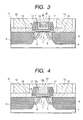
- FIG. 3 is a cross-sectional view of a completed high dielectric gate insulation film field effect transistor according to a third embodiment of this invention.
- FIG. 4 is a cross-sectional view of a completed high dielectric gate insulation film field effect transistor according to a fourth embodiment of this invention.
- FIG. 5 is a graph showing a relation between an SiO 2 film thickness at a high dielectric film/Si substrate boundary and a shift amount ⁇ V FB of a flat band;
- FIG. 6 is a graph showing a relation between a post heat treatment temperature and a shift amount of a flat band voltage (Al 2 O 3 film);
- FIG. 7 is a graph showing a relation between a post heat treatment temperature and a shift amount of a flat band voltage (film other than Al 2 O 3 );
- FIG. 8 is a schematic view of an ECR sputtering apparatus
- FIG. 9 shows XPS spectra of Si2p electrons and Al2p electrons for an Al 2 O 3 /SiO 2 /Si structure
- FIG. 10 is a graph showing a relation between an SiO 2 equivalent film thickness EOT and a high dielectric insulation film thickness of a high dielectric insulation film/SiO 2 /Si capacitor;
- FIG. 11 is a graph showing a relation between an SiO 2 equivalent film thickness EOT and a leak current of a high dielectric insulation film/SiO 2 /Si capacitor;
- FIG. 12 is a cross-sectional view of the sequence of manufacturing steps for a high dielectric gate insulation film field effect transistor according to a first embodiment of this invention.
- FIG. 13 is a cross-sectional view of the sequence of manufacturing steps for a high dielectric gate insulation film field effect transistor according to a first embodiment of this invention
- FIG. 14 is a cross-sectional view of the sequence of manufacturing steps for a high dielectric gate insulation film field effect transistor according to a second embodiment of this invention.
- FIG. 15 is a cross-sectional view of the sequence of manufacturing steps for a high dielectric gate insulation film field effect transistor according to a second embodiment of this invention.
- FIG. 16 is a cross-sectional view of the sequence of manufacturing steps for a high dielectric gate insulation film field effect transistor according to a third embodiment of this invention.
- FIG. 17 is a cross-sectional view of the sequence of manufacturing steps for a high dielectric gate insulation film field effect transistor according to a third embodiment of this invention.
- FIG. 18 is a cross-sectional view of the sequence of manufacturing steps for a high dielectric gate insulation film field effect transistor according to a third embodiment of this invention.
- FIG. 19 is a cross-sectional view of the sequence of manufacturing steps for a high dielectric gate insulation film field effect transistor according to a third embodiment of this invention.
- FIG. 20 is a cross-sectional view of the sequence of manufacturing steps for a high dielectric gate insulation film field effect transistor according to a third embodiment of this invention.
- FIG. 21 is a graph showing the dependence of the mobility on the effective field effect for an N-channel type MISFET using Al 2 O 3 for a gate insulation film.
- the present inventors have made a detailed study regarding (1) the relation between SiO 2 film at the boundary between the high dielectric material and the Si substrate; (2) the FET characteristic and the relation between the FET characteristic and the boundary SiO 2 film forming temperature; and (3) the relation between the FET characteristic and the gate electrode material.
- the SiO 2 film at the boundary between the high dielectric material and the Si substrate, and the FET characteristic are to be described specifically.
- the high dielectric material an Al 2 O 3 film is used as an example.
- the method of preparing Al 2 O 3 is described below. After washing a Si single crystal substrate (resistivity: 10 ⁇ cm, 8 inch) with HF, an Al 2 O 3 film is deposited by an ECR sputtering apparatus at a room temperature. The apparatus is shown in FIG. 8 .
- the amount of Ar and O 2 supplied is controlled by a mass flow meter.
- a microwave at 2.45 GHz is introduced under a constant magnetic field to generate ECR plasmas.
- the microwave power is 500 W.
- sputtering is conducted by applying an RF electric field at 13.56 MHz to an Al ring target.
- the RF power is 500 W.
- an Si substrate is placed remotely from the Al target, and the substrate surface is deflected by 90° relative to the sputtering target surface and located eccentrically.
- the substrate potential is set at a floating potential (i.e., a potential results into net current collection from the plasma). Accordingly, plasma damages are reduced compared with usual DC magnetron sputter apparatus.
- for making the deposition film thickness uniform within the plane it is deposited while rotating a wafer at 25 rpm.
- the apparatus is provided with a shutter mechanism, and a film is deposited after stabilizing ECR plasma discharge or sputtering discharge.
- the pressure in the film deposition chamber is usually at 1 ⁇ 10 ⁇ 4 Pa, and a pressure upon gas introduction is 9 ⁇ 10 ⁇ 2 Pa.
- Sputtering is conducted in a state not oxidizing the surface of the Al target at the supply of Ar of 25 sccm and O 2 of 3.0 sccm.
- the analysis of a 30 nm film formed on Si by auger electron spectroscopy confirms that Al and O were uniformly distributed in the film, and the deposition film was Al 2 O 3 . Accordingly, it appears that the sputtered Al is oxidized with oxygen in the ECR plasmas on the Si substrate and formed into an Al 2 O 3 film.
- the deposition rate of the Al 2 O 3 film is 1.7 ⁇ /s.
- the Al 2 O 3 film is first deposited for 12 sec by using the method described above and, further, applied with heat treatment under vacuum at 450° C. for 10 min in the identical apparatus (Ar atmosphere, pressure: 7 ⁇ 10 ⁇ 4 torr) and then taken out into atmospheric air.
- the delivery method is described below.
- the SiO 2 film thickness is 0.1 nm to 0.2 nm.
- an SiO 2 film is grown on the Al 2 O 3 /Si boundary.
- the Al 2 O 3 film thickness determined by a TEM measurement is 2.0 nm ⁇ 0.1 nm.
- the detection angle of photoelectrons is 30° in the direction parallel with the surface of a specimen.
- the energy position is decided by setting the Si—Si (Si 0+ ) bonding energy of Si substrate appearing in Si2p electron spectra as 99.2 eV. Further, all the numbers of detected Si2p photoelectrons are normalized by the peaks (Al 3+ bonding state of Al 2 O 3 ) with a bonding energy of 75.7 eV observed in common with the Al2p electron spectra.
- SiO 2 bond Si 4+ .
- the electric film thickness EOT of an Al/Al 2 O 3 /SiO 2 /Si capacitor measured after deposition of the Al gate increases correspondingly with (a ratio of 1.0) the increase of the SiO 2 boundary film thickness.
- the EOT film thickness is extrapolated to zero to determine the boundary SiO 2 film thickness. It is confirmed that the boundary SiO 2 film thickness determined based on FIG. 10 and the SiO 2 film thickness determined by using the equation (1) agree to each other with a difference within 0.1 nm.
- Table 1 collectively shows the oxidizing heat treatment conditions for the films shown in FIG. 9 and the SiO 2 film thickness at the boundary determined by the method described above.
- FIG. 5 shows a relation between the boundary SiO 2 film thickness and the shift amount ⁇ V FB of the flat band voltage. It can be seen from FIG. 5 that the voltage shifts by about 3.0 V toward the positive voltage when the SiO 2 film is thin. This shows that negative fixed charges are present in the film. Then, it was found that ⁇ V FB decreases along with increase of the boundary SiO 2 film thickness and disappears where a boundary SiO 2 film is of 0.5 nm or more. In this study, films were examined for the SiO 2 film forming temperature from 300° C. to 1100° C., and it was been confirmed that the characteristics described above do not depend on the temperature for oxidizing heat treatment.
- the mechanism for generating negative fixed charges is to be considered.
- metallic AlO x bonding state state in which O is depleted from Al 2 O 3
- the generation of negative charges is expected in AlO x in a state where Al 2 O 3 is reduced.
- the amount of fixed charges that is estimated in view of ⁇ V FB >3.0 V is 4 ⁇ 10 13 /cm 2 or more.
- the oxygen distribution at the Al 2 O 3 /SiO 2 boundary becomes uniform and the AlO x layer disappears.
- the reason why the AlO x layer is formed when the SiO 2 film is thin is because the Al 2 O 3 /Si boundary can not be as abrupt as the SiO 2 /Si boundary.
- an SiO 2 buffer layer of 0.5 nm or more is necessary for matching Al 2 O 3 with the Si substrate boundary.
- the SiO 2 film thickness is about 0.3 nm, although the AlO x layer disappears in the XPS spectra for Al2p electrons in FIG.
- FIG. 5 shows the relation between the boundary SiO 2 film thickness and the shift amount of the flat band voltage for HfO 2 , ZrO 2 , and La 2 O 3 together. For such films, high speed oxidation treatment is conducted in a pressure-reduced oxygen atmosphere at 300° C.
- the boundary SiO 2 film thickness was controlled by changing the heat treatment time and O 2 partial pressure.
- the SiO 2 film thickness was obtained by XPS spectroscopy, TEM measurement and ellipsometer measurement in the same manner as for the Al 2 O 3 film thickness.
- the gate electrode is Pt. It can be seen from FIG. 1 that 0.5 nm or more of the boundary SiO 2 film is necessary for making the flat band voltage shift to zero also in cases of high dielectric insulation films. It was confirmed that the foregoing conditions are identical also with respect to other rare earth oxides than Y 2 O 3 or, La 2 O 3 , HfSiO 4 and ZrSiO 4 .
- FIG. 6 shows a relation between the post heat treatment temperature and the shift amount of the flat band voltage.
- Each of the films has a boundary SiO 2 film of 0.5 nm to 0.7 nm thickness, and the shift amount of the flat band voltage just after oxidation is zero.
- the film applied with the oxidizing heat treatment for film formation at a temperature of 400° C. did not depend on the forming temperature and no flat band voltage shift was caused as long as the post heat treatment temperature was 750° C. or lower.
- a post heat treatment at 800° C. or higher was conducted, a positive voltage shift was observed for the flat band voltage after the post heat treatment even when a boundary SiO 2 film of 0.5 nm or more was present. It is considered that the oxygen distribution in the Al 2 O 3 /SiO 2 boundary was changed by the high temperature heat treatment.
- the film forming temperature (oxidation treatment temperature) was equal to or higher than the post heat treatment temperature, shift of the flat band voltage was not observed even for a heat treatment temperature of 850° C. or higher.
- a film of a structure having a boundary SiO 2 film of 0.5 nm or more between Al 2 O 3 and Si substrate as the invention is stable also after the post heat treatment at 750° C. or lower and it shows the excellent boundary characteristic.
- the second discovery is a film forming method for forming a boundary SiO 2 film of 0.5 nm or more at the boundary between Al 2 O 3 and Si substrate in an oxidative atmosphere at a temperature higher than the heat treatment temperature in the subsequent step. This can form an insulation film which is stable to a heat treatment at 1100° C. and shows the excellent boundary characteristic.
- an SiO 2 film of 0.6 nm thick can be formed between Al 2 O 3 and Si substrate by applying a rapid thermal oxidation treatment (RTO treatment) at 100° C. for 5 sec in an atmosphere of O 2 partial pressure at 5 torr.
- RTO treatment rapid thermal oxidation treatment
- an SiO 2 film of 0.6 nm thickness can be formed between Al 2 O 3 and Si substrate by applying an RTO treatment at 100° C. for 5 sec in an atmosphere of O 2 partial pressure at 1 torr.
- the second discovery is effective not only to form the Al 2 O 3 but also for forming other high dielectric insulation films.
- a post heat treatment is conducted in an inert atmosphere. Then, a Pt gate electrode is formed and the dependence of the MIS capacitance on the voltage is measured.
- FIG. 7 shows a relation between the temperature for the post heat treatment and the flat band voltage shift amount of the MIS capacitor.
- Each of the films has a boundary SiO 2 film of 0.8 nm thick. The film at an oxidation treatment temperature of 400° C.
- an SiO 2 film of 0.7 nm thickness is grown between the high dielectric insulation film and the Si substrate by applying an RTO treatment at 1000° C. for 5 sec in an atmosphere of O 2 partial pressure at 1 torr.
- an SiO 2 film of 1.0 nm thickness is grown between the high dielectric insulation film and the Si substrate by applying an RTO treatment at 1100° C. for 5 sec in an atmosphere of O 2 partial pressure at 1 torr.
- a necessary boundary SiO 2 film was formed between the high dielectric insulation film and the Si substrate by an oxidation heat treatment after forming the high dielectric insulation film, but it may be formed also before deposition of the high dielectric insulation film.
- a high dielectric insulation film after forming an SiO 2 film of 0.5 nm thickness by thermally oxidizing an Si substrate in an oxidative atmosphere, a film which is stable and shows the excellent boundary property can be formed at a temperature of source-drain activating heat treatment of 750° C. or lower.
- an insulation film having high heat stability and showing excellent boundary characteristic can be formed by controlling the temperature for forming the SiO 2 film to higher than the temperature for the source-drain activating heat treatment.
- a heat treatment under oxidation conditions not further growing a boundary SiO 2 film after forming the high dielectric insulation film.
- the high dielectric insulation film may be formed as below.
- An SiO 2 substrate is applied with an RTO treatment at 1000° C. for 5 sec in an atmosphere of an O 2 partial pressure at 5 torr to form an SiO 2 film of 0.5 nm thickness.
- the RTO treatment is preferably applied at 1000° C. for 5 sec in an atmosphere of an O 2 partial pressure at 1 torr.
- the SiO 2 film between the high dielectric insulation film and the Si substrate can also be replaced with a silicon oxynitrite film (SiON).
- the film forming method is as below.
- a high dielectric insulation film/SiO 2 /Si substrate having an SiO 2 film of 0.5 nm or more is further applied with an NO treatment thereby introducing N near the SiO 2 /Si boundary.
- the NO treatment condition is, for example, a heat treatment for 10 sec in an NO atmosphere at about 900° C.
- an Si substrate is at first oxidized by a heat treatment in an N 2 O atmosphere before deposition of a high dielectric insulation film to form an SiON film of 0.5 nm or more.
- a film which is stable even at an activating heat treatment of 750° C. and shows the excellent boundary characteristic is formed.
- an SiON film of 0.5 nm thickness can be formed under the N 2 O treatment conditions at 1000° C. for 5 sec in an atmosphere of an N 2 O partial pressure at 10 torr.
- a film of excellent thermal stability can be formed by controlling the temperature for forming SiON film at or higher than the activating heat treatment temperature.
- a third method is as described below.
- An Si substrate is nitrided after cleaning with HF at a temperature of 700° C. or lower in an NH 3 atmosphere.
- the nitride film in this case is about one layer on the Si surface.
- a high dielectric insulation film is deposited and applied with a heat treatment in an oxidative atmosphere to form an SiON film of 0.5 nm or more at the boundary between the high dielectric insulation film and Si.
- a film of excellent heat stability can be formed by controlling the heat treatment temperature in the oxidative atmosphere equal to or higher than the activating heat treatment temperature.
- the fourth method is as shown below.
- an SiON film of 0.5 nm or more is formed on the boundary by a heat treatment in an N 2 O atmosphere.
- a film of excellent heat stability can be formed by controlling the heat treatment temperature for the oxidative atmosphere equal to or higher than the activating heat treatment temperature.
- an SiON film of 0.5 nm thickness can be formed by applying a rapid heat treatment at 1000° C. for 5 sec in an atmosphere of an N 2 O partial pressure at 10 torr.
- the N 2 O heat treatment can be replaced with an NO treatment.
- the present inventors at first studied on the Al 2 O 3 gate insulation film using a polycrystalline silicon gate. After depositing an Al 2 O 3 film of 1.5 nm thickness, a rapid heat treatment at 1000° C. for 5 sec was conducted in an atmosphere of an O 2 pressure at 5 torr, to form a boundary SiO 2 film of 0.6 nm thickness, and then a polycrystalline Si gate was formed. Successively, impurity ions were implanted in gate, source and drain regions and a rapid thermal heat treatment was conducted at 1000° C. for 5 sec as an activating heat treatment. Further, after by way of a wire forming step, an MISFET was formed.
- the SiO 2 equivalent thickness of the film was 1.3 nm.
- a flat band voltage shift of +0.3 V was also observed. It is considered that since the boundary between the polycrystalline Si gate electrode and the Al 2 O 3 could not be abrupt, oxygen in Al 2 O 3 slightly diffuses into the polycrystalline Si gate electrode to form an AlO x layer and generate negative fixed charges.
- the mobility of the N-channel type MISFET is degraded to about 3 ⁇ 4 compared with a universal curve of an SiO 2 film (general curve giving effective field effect dependence of the mobility) (in a case of the Al 2 O 3 gate insulation film ⁇ circle around ( 2 ) ⁇ in FIG. 21 ).
- a rapid heat treatment may be conducted at an oxidation heat treatment temperature of higher than the activating thermal heat temperature, for example, 1000° C. in an atmosphere of an O 2 partial pressure at 5 torr for 5 sec.
- an FET with no flat band voltage shift and with no degradation of the mobility (the Al 2 O 3 gate insulation film ⁇ circle around ( 1 ) ⁇ in FIG. 21) by the preparation method described above.
- an SiO 2 film of 0.5 nm or more was necessary to both of the boundary between Al 2 O 3 film and the Si substrate and the boundary between the Al 2 O 3 film and the polycrystalline silicon substrate, this hinders reduction of the thickness of the gate insulation film.
- the SiO 2 equivalent thickness of the gate insulation film formed by the method described above was, for example, 1.6 nm.
- a TiN film by a reactive sputtering method on an Al 2 O 3 film (1.5 nm) formed with a boundary SiO 2 film to a thickness of 0.5 nm
- a W film was deposited by a sputtering method. In this case, no mismatching as observed at the boundary between Al 2 O 3 and the polycrystalline silicon gate was formed, and excellent boundary characteristic could be maintained.
- the SiO 2 equivalent film thickness of the MIS capacitor was 1.2 nm.
- the TiN film is necessary for preventing reaction between the gate insulation film and W, which can be replaced with a conductive barrier film such as WN, MoN, TaN, ZrN and HfN.
- the W electrode may also be replaced with an Mo electrode.
- the W electrode may also be replaced with an Mo electrode.
- an FET stable to thermal load in the subsequent step can be formed.
- the boundary SiO 2 film may be replaced with an SiON film.
- HfO 2 film An HfO 2 film of 3.0 nm thickness was deposited by an ALCVD method using HfCl 4 and H 2 O. The substrate temperature was 300° C. After the deposition, a rapid heat treatment at 1050° C. for 5 sec was conducted in an atmosphere of an O 2 partial pressure at 1 torr to form a boundary SiO 2 film of 0.8 nm thickness and then a polycrystalline Si gate was formed.
- impurity ions were implanted into gate, source and drain regions and a rapid heat treatment at 1050° C. for one sec was conducted as an activating heat treatment. Further, after by way of a wire forming step, an MISFET was formed. As a result of measuring dependence of the capacitance of MIS capacitor on the voltage, the SiO 2 equivalent thickness of the film was 1.5 nm. Further, the flat band voltage shift amount was 0.1 V or less and the mobility of the MISFET was substantially identical with a universal curve of an SiO 2 film (general curve giving an effective field effect dependence of the mobility). The foregoing result shows that matching property between the polycrystalline Si gate electrode and HfO 2 is excellent over Al 2 O 3 .
- the reaction layer was not observed but it was confirmed that a film of excellent boundary characteristic could be formed.
- a high melting temperature metal material can also be used instead of the polycrystalline silicon for the gate electrode.
- the excellent boundary characteristic can be maintained by stacking a conductive barrier film such as made of TiN, WN, MoN, TaN, ZrN or HfN, and a metal such as W or Mo on the high dielectric insulation film.
- a boundary SiO 2 film is formed between the high dielectric insulation film and the Si substrate at an oxidation treatment temperature higher than the activating heat treatment temperature, an FET stable to thermal load is formed. Further, the effect of the boundary SiO 2 film can be obtained also with an SiON film.
- a stacked film of an Al 2 O 3 film and a high dielectric insulation film other than Al 2 O 3 can also be used.
- the preparation method is the same as described below.
- Al 2 O 3 of 0.5 nm thickness for example, by an ALCVD method on an Si substrate
- HfO 2 film of 3.0 nm thickness is deposited by the ALCVD method.
- a rapid heat treatment at 1050° C. for 5 sec in an atmosphere of a pressure-reduced oxygen at 5 torr is conducted to form an SiO 2 film of 0.5 nm thickness at the Al 2 O 3 /Si boundary.
- a polycrystalline Si gate or high melting temperature metal gate was formed by the method described above.
- the SiO 2 equivalent film thickness of the MIS capacitor was 1.3, nm and the flat band voltage shift amount thereof was zero. Further, it was confirmed that the mobility of the N-conductivity type or P-conductivity type MISFET was not degraded. Excellent boundary characteristic was also shown when ZrO 2 was used (instead of the HfO 2 film).
- FIG. 10 shows a relation between the SiO 2 equivalent film thickness (EOT) and the thickness of the high dielectric insulation films.
- this invention concerns a structure of a gate insulation film that provides an FET with excellent boundary characteristic and a film forming method thereof, particularly, an SiO 2 (SiON) film at the boundary between the high dielectric insulation film and the Si substrate and a film forming method thereof. Accordingly, while the high dielectric insulation film was deposited by oxidation of metal film, ECR sputtering and ALCVD method in the foregoings. It is apparent that the method is not restricted only thereto.
- FIG. 1 is a cross-sectional view of a completed semiconductor device according to a first embodiment of this invention and FIG. 12 and FIG. 13 are cross-sectional views showing the sequence of production steps thereof.
- a semiconductor substrate 1 comprising single crystalline Si of crystal orientation (100), P-conductivity type and 20 cm diameter was formed with an inter-device isolation region (not illustrated) for defining an active region and applied with ion implantation of P-conductivity type ions for controlling the substrate concentration, heat treatment time, ion implantation (for controlling the threshold voltage and the source-drain activating heat treatment by known methods).
- an Al 2 O 3 film of 1.0 nm thick was deposited at 350° C. by an atom layer deposition CVD method (ALCVD method) using trimethyl aluminum [Al (CH 3 ) 3 ] as a starting material gas and H 2 O as an oxidizing gas.
- ACVD method atom layer deposition CVD method
- an SiO 2 film was formed to 0.5 nm thickness in the same apparatus by the ALCVD method using Si 2 H 6 and H 2 O. Then, a first SiO 2 film 2 of 0.6 nm thickness was formed between Al 2 O 3 and an Si substrate by applying an RTO treatment at 1000° C. for 5 sec in an atmosphere of an O 2 partial pressure at 5 torr.
- a gate insulation film formed of the first SiO 2 film 2 between Al 2 O 3 and the Si substrate, a high dielectric insulation film 3 (Al 2 O 3 of 1.0 nm thickness) and a second SiO 2 film 4 of 0.5 nm thickness on the Al 2 O 3 film could be formed.
- in-situ phosphorus-doped polycrystalline Si film 5 of 100 nm thickness as a gate electrode 5 was formed.
- the in-situ phosphorus-doped polycrystalline Si film 5 was formed by using monosilane (SiH 4 ) and phosphine (PH 3 ) and deposited at a temperature of 630° C. (FIG. 12 ).
- the polycrystalline Si film 5 was formed by selectively implanting ions at high concentration to a desired gate electrode region based on the known manufacturing method for complementary MOS instead of the previously adding impurities. Successively, after conducting a heat treatment for 5 min in a nitrogen atmosphere at 750° C., the in-situ phosphorus-doped polycrystalline Si film 5 was made into the gate electrode.
- As ions were implanted at an acceleration energy of 3 keV and at an injection amount of 1 ⁇ 10 15 /cm 2 to form a shallow diffusion layer 6 .
- B ions were implanted in the vertical direction at an acceleration energy of 10 keV and an injection amount of 4 ⁇ 10 13 /cm 2 so as to surround the shallow diffusion layer 6 to form a P-conductivity type punch-through preventive diffusion layer 7 for preventing punch-through.
- an activating heat treatment for implanted ions was conducted by nitrogen annealing at 1000° C. for 5 sec. Further, a thin Co film was deposited over the entire surface by sputtering, and silicidation was applied by a short time annealing at 500° C. An unreacted Co film was removed with a mixed solution of hydrochloric acid and aqueous hydrogen peroxide to selectively leave a Co silicide film 10 on an exposed Si substrate portion, and then a short-time heat treatment was applied to reduce the resistance of the Co silicide film 10 . Then, after forming a thick silicon oxide deposition layer over the entire surface, the surface was flattened by chemical mechanical polishing to form a surface protection insulation film 11 .
- a TiN film as a diffusion barrier material for the wiring metal and a W film as the wiring metal were deposited, and the W film was left selectively only at the opened portion by the flattening polishing thereof.
- wirings including source and drain electrodes 12 were formed by deposition and patterning of a metal film comprising aluminum as a main material in accordance with a desired circuit structure to form a field effect transistor (FIG. 1 ).
- An MISFET so formed has an SiO 2 equivalent film thickness of 1.6 nm. As shown by the relation between the SiO 2 boundary film thickness at the Al 2 O 3 /Si boundary and a flat band voltage shift in FIG.
- a gate insulation film with no fixed charges can be formed by forming an SiO 2 film of 0.5 nm thickness or more at the Si and Al 2 O 3 boundary. Further, as shown by the relation between the temperature of the activating heat treatment and the amount of flat band voltage shift in FIG. 6, an FET showing excellent boundary characteristic with no degradation of the carrier mobility could be formed by controlling the oxidation heat treatment condition upon forming the gate insulation film at a temperature higher than the source-drain activating heat treatment temperature for a source and drain. In a case where the activating heat treatment temperature for the source-drain in the method described above is 1050° C. for one sec, it is necessary that the oxidizing heat treatment upon forming the gate insulation film is an RTO treatment to be applied at 1050° C. for 5 sec in an atmosphere of an O 2 partial pressure at 1 torr.
- ZrO 2 or HfO 2 is applicable instead of Al 2 O 3 .
- a ZrO 2 film of 2.0 nm thickness is deposited by an atom layer deposition CVD method (ALCVD method) using ZrCl 4 as a starting material gas and H 2 O as an oxidizing gas at 300° C. Further, in the same apparatus, An SiO 2 film was formed to 0.5 nm thickness by an ALCVD method using Si 2 H 6 and H 2 O. Then, an SiO 2 film 2 of 0.8 nm thickness was formed between ZrO 2 and the Si substrate by applying an RTO treatment at 1050° C. for 5 sec in an atmosphere of an O 2 partial pressure at 5 torr.
- a gate insulation film formed of an SiO 2 film 2 of 0.8 nm thickness between ZrO 2 and the Si substrate, a dielectric insulation film 3 (2.0 nm, ZrO 2 ), and an SiO 2 film 4 of 0.5 nm thickness on the ZrO 2 film could be formed.
- the subsequent preparation method is identical with that has been described above.
- an MISFET structure with the SiO 2 equivalent film thickness of 1.8 nm (FIG. 1) can be formed. As shown in FIG. 5 and FIG.
- an FET with no degradation of the carrier mobility and showing excellent boundary characteristic could be formed by the formation of the SiO 2 film of 0.5 nm or more on the Si/ZrO 2 boundary and setting the condition for the oxidizing thermal treatment upon forming the gate insulation film to a temperature higher than the activation heat treatment temperature for a source-drain.
- comparable characteristics could be obtained by depositing an HfO 2 film of 2.0 nm thickness by an ALCVD method using HfCl 4 and H 2 O and forming an MISFET by the same method as described above.
- an SiO 2 film 2 of 0.7 nm thickness can be grown between the high dielectric insulation film 3 and the Si substrate 1 by applying an RTO treatment at 1000° C. for 5 sec in an atmosphere of an O 2 partial pressure at 1 torr.
- an SiO 2 film 2 of 1.0 nm thickness can be grown between the high dielectric insulation film 3 and the Si substrate 1 by applying an RTO treatment at 1100° C. for 5 sec in an atmosphere of an O 2 partial pressure at 1 torr.
- the SiO 2 layer 4 at the boundary between the high dielectric insulation film 3 and the polycrystalline silicon 5 necessary for the gate insulation film structure of the semiconductor device could also be formed by the following method. Description is made referring to an HfO 2 film as an example. An HfO 2 film of 2.0 nm thickness was deposited by an ALCVD method using HfCl 4 and H 2 O. The substrate temperature was 300° C. A rapid heat treatment was conducted at 1050° C. for 5 sec in an atmosphere of an O 2 pressure at 1 torr to form a boundary SiO 2 film 2 to 0.8 nm thickness and then a polycrystalline Si gate 5 was formed. Further, in the same manner as described above, a rapid heat treatment was conducted at 1000° C.
- the amount of the flat band voltage shift was about 0.1 V or less, and the electron mobility of MISFET substantially conformed with a universal curve of the SiO 2 film (general curve giving an effective field effect dependence of the mobility).
- the gate insulation film could suppress the leak current to ⁇ fraction (1/1000) ⁇ or less compared with existent SiO 2 films.
- the MIS capacitor showed a flat band voltage shift of 0.3 V toward the positive voltage. Further, the carrier mobility was degraded by 25% compared with a case where the SiO 2 film 4 was present.
- boundary layer mainly comprising SiO 2 (a buffer layer) to maintain the matching property between the HfO 2 film 3 and the polycrystalline silicon 5 so as to suppress the generation of fixed charges.
- the boundary layer was formed in a case where the heat treatment after the formation of the polycrystalline silicon was 700° C. or higher. Accordingly, this is considered that oxygen in the HfO 2 film 3 and the SiO 2 film, and the polycrystalline Si gate were reacted by a high temperature heat treatment.
- the second SiO 2 layer 4 at the boundary between the high dielectric insulation film 3 and the polycrystalline silicon 5 could be formed without deposition. Further, the second boundary SiO 2 layer 4 could be formed also with ZrO 2 rather than HfO 2 .
- the necessary first boundary SiO 2 film between the high dielectric insulation film and the Si substrate was formed by the oxidation heat treatment after forming the high dielectric insulation film, it is also possible to form before deposition of the high dielectric insulation film.
- a film which was stable and showing excellent boundary characteristic could be formed also at a subsequent post heat treatment at 750° C. or lower by depositing a high dielectric insulation film after forming the first SiO 2 film to 0.5 nm thickness with oxidizing the Si substrate by a heat treatment in an oxidative atmosphere.
- an insulation film which was highly heat-stable and showing excellent boundary characteristics could be formed by setting the temperature for forming the first SiO 2 film to a temperature higher than that of the post heat treatment.
- a heat treatment is conducted under such an oxidative atmosphere not to grow the first boundary SiO 2 film further after forming the high dielectric insulation film.
- the first SiO 2 film between the high dielectric insulation film and the Si substrate can also be replaced with a silicon oxynitrite film (SiON).
- the film forming method is as below.
- a high dielectric insulation film/SiO 2 /Si substrate having a first SiO 2 film of 0.5 nm or more formed by the method described above was further applied with an NO treatment thereby introducing N near the SiO 2 /Si boundary.
- the NO treatment condition was, for example, a heat treatment for 10 sec in an NO atmosphere at about 900° C.
- an Si substrate was at first oxidized by a heat treatment in an N 2 O atmosphere before deposition of a high dielectric insulation film, to form an SiON film of 0.5 nm or more.
- a film which was stable even at a post heat treatment of 800° C. and has excellent boundary characteristic could be formed.
- an SiON film of 0.5 nm thickness could be formed at 1000° C. for 5 sec in an atmosphere of an N 2 O partial pressure at 10 torr.
- a film of excellent thermal stability could be formed by controlling the temperature for forming SiON film to higher than the source-drain activating heat treatment temperature.
- a third method is as described below.
- An Si substrate was nitrided after cleaning with HF at a temperature of 700° C. or lower in an NH 3 atmosphere.
- the nitride film in this case comprised about one layer on the Si surface.
- a high dielectric insulation film was deposited and applied with a heat treatment in an oxidative atmosphere to form an SiON film of 0.5 nm or more at the boundary between the high dielectric insulation film and Si.
- a film of excellent heat stability could be formed by controlling the heat treatment temperature in the oxidative atmosphere to higher than the post heat treatment temperature.
- a fourth method is as shown below.
- an SiON film of 0.5 nm or more was formed on the boundary by a heat treatment in an N 2 O atmosphere.
- a film of excellent heat stability could be formed by controlling the heat treatment temperature in the oxidative atmosphere to be higher than the post heat treatment temperature.
- an SiON film of 0.5 nm thickness could be formed by applying a rapid heat treatment at 1000° C. for 5 sec in an atmosphere of an N 2 O partial pressure at 10 torr.
- the N 2 O heat treatment can be replaced with NO treatment.
- an rare earth oxide film such as Al 2 O 3 , HfO 2 , ZrO 2 , Y 2 O 3 , or La 2 O 3 can be formed by an ECR sputtering method using a metal target corresponding to a desired metal oxide.
- the outline of the ECR sputtering apparatus is as shown in FIG. 8 .
- Ar supplied amount was controlled to 25 sccm
- O 2 supplied amount was controlled to 3.0 sccm by a mass flow meter.
- microwaves at 2.45 GHz was introduced under a constant magnetic field to generate ECR plasmas.
- the microwave power was 500 W.
- sputtering could be conducted without oxidizing the surface of the metal target but by applying an RF electric field at 13.56 MHz to the metal ring target.
- RF power was 500 W.
- the substrate After depositing a high dielectric insulation film by controlling the deposition time so as to obtain a desired film thickness and applying a heat treatment in vacuum at 200° C. to 500° C. in the same apparatus (Ar atmosphere, pressure; 7 ⁇ 10 ⁇ 4 torr), the substrate may be taken out to the atmospheric air.
- high dielectric insulation film can also be formed by a low temperature oxidation at 400° C. or lower.
- HfSiO 4 ZrSiO 4
- HfCl 4 ZrCl 4
- SiH 4 the starting material
- H 2 O an oxidizing gas
- FIG. 2 is a cross-sectional view showing a completed field effect transistor according to a second embodiment of this invention
- FIG. 14 and FIG. 15 are schematic views for the production steps thereof.
- a high melting metal gate was applied instead of the polycrystalline silicon gate.
- a semiconductor substrate 1 comprising single crystalline Si having crystal orientation (100), P-conductivity type and of 20 cm diameter was formed with an inter-device isolation region (not illustrated) for defining an active region and applied with implantation of P-conductivity type ions for controlling the substrate concentration, extended heat treatment time, and ion implantation for controlling the threshold voltage and activating heat treatment by known methods.
- an Al 2 O 3 film was formed to a thickness of 1.5 nm by an ECR sputtering method.
- the ECR sputtering method is as shown in Example 1. However, sputtering time for forming the Al 2 O 3 of 1.5 nm thickness was set to 9 sec.
- an SiO 2 film of 0.6 nm thickness was formed between the Al 2 O 3 film 3 and the Si substrate 1 by applying an RTO treatment at 1000° C. for 5 sec in an atmosphere of an O 2 particle pressure at 5 torr.
- a boundary SiON film 2 of 0.7 nm thickness was formed between the Al 2 O 3 film 3 and the Si substrate 1 by conducting rapid heat treatment at 900° C. for 10 sec in an NO atmosphere.
- An SiO 2 film may be used instead of the SiON film.
- a TaN gate electrode 13 a as a high melting metal nitride was formed by a reactive sputtering method. TiN, WN, MoN, ZrN or HfN may be used instead of TaN. Further, a W gate 13 b (or Mo) as a high melting metal was formed by a sputtering method or CVD method (FIG. 14 ). Further, gate electrodes 13 a , 13 b were formed by etching using a photoresist film as a mask. As ions were implanted at an acceleration energy of 3 keV and an implantation amount of 1 ⁇ 10 15 /cm 2 to form a shallow diffusion layer 6 .
- B ions were implanted in the vertical direction so as to surround the shallow diffusion layer 6 at an acceleration energy of 10 keV and an implantation amount of 4 ⁇ 10 13 /cm 2 to form a P-conductivity type punch-through preventive diffusion layer 7 for preventing punch-through.
- a silicon oxide film of 50 nm thickness over the entire surface at a low temperature of 400° C. by a plasma-assisted deposition method, it was selectively left only on the side wall of the gate electrode 3 by anisotropic dry etching to form a gate side wall insulation film 8 .
- an activating heat treatment for implanted ions was applied by nitrogen annealing at 1000° C. for 5 sec. Further, a thin Co film was deposited over the entire surface by sputtering, and silicidation was applied by a short-time annealing at 500° C. After removing an unreacted Co film with a mixed solution of hydrochloric acid and aqueous hydrogen peroxide to selectively leave the Co silicide film 9 on an Si substrate exposed portion, reduction of resistance for the Co silicide film 10 was achieved by a short-time heat treatment. Then, after forming a thick silicon oxide deposition film over the entire surface, the surface was flattened by chemical mechanical polishing to form a surface protection insulation film 11 .
- a TiN film as a diffusion barrier material for the wiring metal and a W film as the wiring metal were deposited, which were flattened by polishing to selectively leave the W film only in the opened portion.
- deposition of a metal film made of aluminum as a main material and patterning thereof were applied in accordance with a desired circuit constitution to form wirings including drain and source electrodes 12 to manufacture a field effect transistor (FIG. 2)
- a MOSFET with an equivalent SiO 2 thickness of 1.3 nm could be formed.
- a gate insulation film with no fixed charges could be formed by forming a first SiO 2 (SiON) film 2 of 0.5 mm or more at the boundary between the Si substrate 1 and the Al 2 O 3 film 3 . Further, since the matching property at the boundary between the Al 2 O 3 film 3 and the nitride 13 a of high melting metal was satisfactory, no fixed charges were generated. Further, as shown by the relation between the post heat treatment temperature and the shift amount of the flat band voltage in FIG. 6, an FET with no degradation of carrier mobility and showing the excellent boundary characteristic could be formed by setting the oxidation heat treatment temperature upon forming the gate insulation film higher than the activating heat treatment temperature for a source-drain. In the method described above, the leak current could be suppressed to ⁇ fraction (1/500) ⁇ compared with that of the SiO 2 film, by forming the boundary between the Si substrate 1 and the Al 2 O 3 film 3 with the SiON film 2 .
- a rare earth oxide such as HfO 2 , ZrO 2 , Y 2 O 3 , La 2 O 3 , HfSiO 4 , or ZrSiO 4 film may also be used.
- the step of forming the boundary SiO 2 (SiON) film 2 at the boundary between the high dielectric insulation film 3 and the Si substrate 1 is the same as described in Embodiment 1. However, since the high dielectric insulation film, such as the Al 2 O 3 film, had a satisfactory boundary matching property with the high melting metal nitride 13 a , the SiO 2 was not required between the high dielectric insulation film 3 and the high melting metal nitride 13 a .
- the step of forming the FET after forming the high melting metal nitride 13 a is the same as described in Embodiment 1.
- an SiO 2 (SiON) film is formed to 0.5 nm or more at the boundary between the Si substrate and the high dielectric insulation film and the temperature for forming the SiO 2 film is set higher than the temperature in the subsequent step, a film of excellent boundary characteristic can be formed.
- FIG. 3 is a cross sectional view showing a completed field effect transistor in a third embodiment according to this invention and FIG. 16 to FIG. 20 are schematic views for manufacturing steps thereof.
- an activating heat treatment was applied for implanted ions before formation of the gate insulation film thereby mitigating the thermal load on a high dielectric insulation film.
- a semiconductor substrate 1 comprising single crystalline Si having crystal orientation (100), P-conductivity type and of 20 cm diameter was applied with formation of the inter-device isolation region (not illustrated) for defining an active region, implantation of P-conductivity type ions for controlling the substrate concentration, heat treatment time, and ion implantation (for controlling the threshold voltage and an activating heat treatment by known methods), and then a thermal oxide film 14 was formed to 5 nm thickness. Then, after depositing an amorphous non-doped Si film 15 to 150 nm thickness on the thermal oxide film 14 , a silicon oxide deposition film was deposited by 50 nm thickness to form a surface protection insulation film 11 .
- a dummy gate electrode 16 was formed by using known lithography and etching.
- P ions were implanted in the vertical direction at an impurity concentration of about 1 ⁇ 10 20 /cm 3 to form a shallow diffusion layer 6 .
- a heat treatment was applied at 1050° C. for 1 sec to activate the implanted impurities.
- B ions were implanted so as to surround the shallow diffusion layer 6 to form a P-conductivity type punch-through preventive diffusion layer 7 for preventing punch-through (FIG. 16 ).
- annealing was conducted in a nitrogen atmosphere at 800° C. for 30 min. Then, the entire surface was flattened by chemical mechanical polishing to expose the upper surface of the dummy gate electrode 16 . Subsequently, after selectively removing the dummy gate electrode 16 , the exposed portion of the SiO 2 insulation film 14 was removed the by using diluted hydrofluoric acid to form an opening 18 (FIG. 19 ).
- a high dielectric insulation film was deposited in the opening 18 by a CVD method of excellent coverage.
- a CVD method of excellent coverage for example, in a case of an Al 2 O 3 film, an Al 2 O 3 film of 1.0 nm thickness was deposited at 350° C. by an atom layer deposition CVD method (ALCVD method) using trimethyl aluminum [Al (CH 3 ) 3 ] as a starting material gas and H 2 O as an oxidizing gas.
- an SiO 2 film 4 was formed to 0.5 nm thickness by an ALCVD method using Si 2 H 6 and H 2 O. Then, a first SiO 2 film 2 of 0.5 nm thickness was formed between Al 2 O 3 and the Si substrate by applying an RTO treatment at 700° C. for 60 sec in an atmosphere of an O 2 partial pressure at 100 torr.
- a gate insulation film comprising an SiO 2 film 2 of 0.5 nm thickness between Al 2 O 3 and the Si substrate, a high dielectric insulation film 3 (Al 2 O 3 of 1.5 nm thickness) and a second SiO 2 film 4 of 0.5 nm thickness on the Al 2 O 3 film could be formed.
- the gate insulation film was formed by using an ALCVD method as described.
- a ZrO 2 film a ZrO 2 film of 2.0 nm thickness was deposited by an ALCVD method using ZrCl 4 and H 2 O as the starting material and the reaction gas.
- the deposition temperature was 300° C.
- a first SiO 2 film 2 of 0.6 nm thickness could be formed between the ZrO 2 film and the Si substrate by applying an RTO treatment at 700° C. for 20 sec in an atmosphere of an O 2 partial pressure at 10 torr.
- the heat treatment temperature and time for forming the first SiO 2 film at the boundary between the high dielectric insulation film 3 and the Si substrate 1 was so set as not to change the impurity profile of the diffusion layer.
- an in-situ phosphorus-doped polycrystalline Si film 5 as a gate electrode 5 was deposited to 100 nm thickness in the opening 18 at a temperature of 630° C. by using monosilane (SiH 4 ) and phosphine (PH 3 ).
- tungsten nitride of 5 nm thickness by a reactive sputtering method to form a WN x barrier layer 19
- tungsten W of 50 nm thickness was deposited by sputtering to form a W gate electrode 20 .
- the entire surface was flattened by chemical mechanical polishing to form a transistor structure applied with embedding fabrication (FIG. 20 ).
- a TiN film as a diffusion barrier material for the wiring metal and a W film as the wiring metal were deposited, which were flattened by polishing to selectively leave the W film only in the opened portion.
- deposition of a metal film made of aluminum as a main material and patterning thereof were conducted in accordance with a desired circuit pattern to form wirings including source-drain electrodes 12 and a gate electrode wiring 21 to manufacture a filed effect transistor (FIG. 3 ).
- the SiO 2 film at the boundary between the in-situ phosphorus-doped polycrystalline Si film 5 and the ZrO 2 film 3 was formed by reaction therebetween upon activating heat treatment at 700° C.
- the SiO 2 layer 4 was formed at the boundary in the same manner as using HfO 2 .
- the above-mentioned processing does not restricted to ZrO 2 .
- HfSiO 4 or ZrSiO 4 it was confirmed that although the reaction layer was not observed a film of excellent boundary characteristic could be formed.
- the SiO 2 equivalent film thickness of the capacitor was, for example, 1.5 nm in a case where the high dielectric insulation film 3 was an Al 2 O 3 film, 1.2 nm in a case it was a ZrO 2 film or HfO 2 film, and 1.4 nm in a case of HfSiO 4 or ZrSiO 4 . Further, no degradation of mobility was observed and an FET having excellent boundary characteristic could be obtained.
- the first SiO 2 film between the high dielectric insulation film and the Si substrate may be replaced with a silicon oxynitride film (SiON).
- SiON silicon oxynitride film
- the film forming steps in this case is the same as in Embodiment 1.
- the temperature of the heat treatment for forming the SiON film at the boundary between the high dielectric insulation film 3 and the Si substrate 1 is so adjusted as not to change the impurity profile of the diffusSi substrate.
- the forming temperature is adjusted to be lower than the activating temperature so as not to change the impurity profile since the S/D activation is done before the formation of the gate insulator.
- the formation time can also be adjusted so as not to change the impurity profile in conjunction with the formation temperature.
- An FET of excellent boundary characteristic could be formed by forming an SiO 2 (SiON) film to 0.5 nm or more at the boundary between the Si substrate and the high dielectric insulation film according to this invention.
- FIG. 4 is a cross sectional view of a completed field effect transistor of Embodiment 4 according to this invention.
- a Co silicide film 10 was formed on source and drain regions to manufacture a structure 18 in which a channel area was opened as shown in FIG. 19 by the same step as in Embodiment 3.
- a high dielectric insulation film was deposited in the opening 18 by the CVD process of excellent coverage by the same step as in Embodiment 3.
- an Al 2 O 3 film of 1.5 nm thickness was deposited at 350° C. by an atom layer deposition CVD method (ALCVD method) using trimethyl aluminum [Al (CH 3 ) 3 ] as a starting material gas and H 2 O as an oxidizing gas.
- an SiO 2 film 2 of 0.5 nm thickness was formed between Al 2 O 3 and the Si substrate by applying an RTO treatment at 700° C. for 60 sec in an atmosphere of an O 2 partial pressure at 100 torr.
- a gate insulation film comprising an SiO 2 film 2 of 0.5 nm thickness between Al 2 O 3 and the Si substrate and a high dielectric insulation film 3 (Al 2 O 3 of 1.50 nm thickness) could be formed.
- the gate insulation film was formed by using an ALCVD method as described below.
- a HfO 2 film of 3.0 nm thickness was deposited by an ALCVD method using HfCl 4 and H 2 O as the starting material and the reaction gas.
- the deposition temperature was 300° C.
- An SiO 2 film 2 of 0.6 nm thickness was formed between the HfO 2 film and the Si substrate by applying an RTO treatment at 700° C. for 20 sec in an atmosphere of an O 2 pressure at 10 torr.
- the heat treatment temperature for forming the SiO 2 film at the boundary between the high dielectric insulation film 3 and the Si substrate 1 was set to such temperature and time as not changing the impurity profile of the diffusion layer.
- TaN to form a high melting metal nitride film 13 a was vapor deposited to 20 nm thickness in the opening 18 by using an ALCVD method. While TaN was used in this Embodiment 4, it may be TiN, WN, MoN, ZrN or HfN. Further, W or Mo was formed as a high melting metal film 13 b by sputtering or CVD. Subsequently, after forming a thick silicon oxide deposition film over the entire surface, it was flattened entirely by chemical mechanical polishing to form a transistor structure applied with embedding fabrication.
- a TiN film as a diffusion barrier material for the wiring metal and a W film as the wiring metal were deposited, which were flattened by polishing to leave the W film selectively only in the opening portion.
- deposition of a metal film made of aluminum as a main material and patterning thereof were conducted in accordance with a desired circuit pattern to form wirings including source-drain electrodes 12 and a gate electrode wiring 21 to manufacture a field effect transistor (FIG. 4 ).
- the SiO 2 equivalent film thickness of the capacitor was, for example, 1.2 nm in a case where the high dielectric insulation film is an Al 2 O 3 film, 1.1 nm in a case it was a ZrO 2 or HfO 2 film, and 1.2 nm in a case it was HfSiO 4 or ZrSiO 4 .
- the SiO 2 equivalent film thickness of the capacitor was, for example, 1.2 nm in a case where the high dielectric insulation film is an Al 2 O 3 film, 1.1 nm in a case it was a ZrO 2 or HfO 2 film, and 1.2 nm in a case it was HfSiO 4 or ZrSiO 4 .
- the SiO 2 equivalent film thickness of the capacitor was, for example, 1.2 nm in a case where the high dielectric insulation film is an Al 2 O 3 film, 1.1 nm in a case it was a ZrO 2 or HfO 2 film, and 1.2 nm in
- the first SiO 2 film between the high dielectric insulation film and the Si substrate may be replaced with the silicon oxynitride film (SiON).
- the film forming steps in this case are the same as in Embodiment 1.
- An FET of excellent boundary characteristic could be formed by forming the first SiO 2 (SiON) film to 0.5 nm or more at the boundary between the Si substrate and the high dielectric insulation film according to this invention.
- the field effect transistor of this Embodiment 4 since capacitance was not decreased by depletion in the gate electrode to the capacitance-voltage characteristic, it was also found that the capacitance is increased compared with known field effect transistors using polycrystalline Si.
Landscapes
- Engineering & Computer Science (AREA)
- Physics & Mathematics (AREA)
- Condensed Matter Physics & Semiconductors (AREA)
- General Physics & Mathematics (AREA)
- Manufacturing & Machinery (AREA)
- Computer Hardware Design (AREA)
- Microelectronics & Electronic Packaging (AREA)
- Power Engineering (AREA)
- Chemical & Material Sciences (AREA)
- Chemical Kinetics & Catalysis (AREA)
- Crystallography & Structural Chemistry (AREA)
- General Chemical & Material Sciences (AREA)
- Optics & Photonics (AREA)
- Insulated Gate Type Field-Effect Transistor (AREA)
- Formation Of Insulating Films (AREA)
- Electrodes Of Semiconductors (AREA)
Priority Applications (2)
| Application Number | Priority Date | Filing Date | Title |
|---|---|---|---|
| US10/900,430 US7119407B2 (en) | 2001-08-27 | 2004-07-28 | Semiconductor device and manufacturing method thereof |
| US11/516,629 US20070001244A1 (en) | 2001-08-27 | 2006-09-07 | Semiconductor device and manufacturing method thereof |
Applications Claiming Priority (2)
| Application Number | Priority Date | Filing Date | Title |
|---|---|---|---|
| JP2001255454A JP2003069011A (ja) | 2001-08-27 | 2001-08-27 | 半導体装置とその製造方法 |
| JPP2001-255454 | 2001-08-27 |
Related Child Applications (1)
| Application Number | Title | Priority Date | Filing Date |
|---|---|---|---|
| US10/900,430 Continuation US7119407B2 (en) | 2001-08-27 | 2004-07-28 | Semiconductor device and manufacturing method thereof |
Publications (2)
| Publication Number | Publication Date |
|---|---|
| US20030042557A1 US20030042557A1 (en) | 2003-03-06 |
| US6787451B2 true US6787451B2 (en) | 2004-09-07 |
Family
ID=19083420
Family Applications (3)
| Application Number | Title | Priority Date | Filing Date |
|---|---|---|---|
| US10/216,792 Expired - Lifetime US6787451B2 (en) | 2001-08-27 | 2002-08-13 | Semiconductor device and manufacturing method thereof |
| US10/900,430 Expired - Lifetime US7119407B2 (en) | 2001-08-27 | 2004-07-28 | Semiconductor device and manufacturing method thereof |
| US11/516,629 Abandoned US20070001244A1 (en) | 2001-08-27 | 2006-09-07 | Semiconductor device and manufacturing method thereof |
Family Applications After (2)
| Application Number | Title | Priority Date | Filing Date |
|---|---|---|---|
| US10/900,430 Expired - Lifetime US7119407B2 (en) | 2001-08-27 | 2004-07-28 | Semiconductor device and manufacturing method thereof |
| US11/516,629 Abandoned US20070001244A1 (en) | 2001-08-27 | 2006-09-07 | Semiconductor device and manufacturing method thereof |
Country Status (3)
| Country | Link |
|---|---|
| US (3) | US6787451B2 (enExample) |
| JP (1) | JP2003069011A (enExample) |
| TW (1) | TW564549B (enExample) |
Cited By (7)
| Publication number | Priority date | Publication date | Assignee | Title |
|---|---|---|---|---|
| US20040126944A1 (en) * | 2002-12-31 | 2004-07-01 | Pacheco Rotondaro Antonio Luis | Methods for forming interfacial layer for deposition of high-k dielectrics |
| US20050045959A1 (en) * | 2001-11-30 | 2005-03-03 | Satoshi Sakai | Semiconductor intergrated circuit device and manufacturing method thereof |
| US20050085092A1 (en) * | 2003-10-16 | 2005-04-21 | Adetutu Olubunmi O. | Multi-layer dielectric containing diffusion barrier material |
| US20060102968A1 (en) * | 2004-11-15 | 2006-05-18 | International Business Machines Corporation | Nitrogen-containing field effect transistor gate stack containing a threshold voltage control layer formed via deposition of a metal oxide |
| US20060192271A1 (en) * | 2005-02-28 | 2006-08-31 | Infineon Technologies Ag | Method of manufacturing a dielectric layer and corresponding semiconductor device |
| US9876069B1 (en) * | 2017-05-18 | 2018-01-23 | Vanguard International Semiconductor Corporation | High-voltage semiconductor device and method for manufacturing the same |
| US10680071B2 (en) * | 2017-05-19 | 2020-06-09 | Renesas Electronics Corporation | Method of manufacturing a semiconductor device using a metal oxide film |
Families Citing this family (45)
| Publication number | Priority date | Publication date | Assignee | Title |
|---|---|---|---|---|
| US6806145B2 (en) * | 2001-08-31 | 2004-10-19 | Asm International, N.V. | Low temperature method of forming a gate stack with a high k layer deposited over an interfacial oxide layer |
| US6787440B2 (en) * | 2002-12-10 | 2004-09-07 | Intel Corporation | Method for making a semiconductor device having an ultra-thin high-k gate dielectric |
| JP4489368B2 (ja) * | 2003-03-24 | 2010-06-23 | 株式会社日立製作所 | 半導体装置およびその製造方法 |
| JP4933256B2 (ja) * | 2003-07-31 | 2012-05-16 | 東京エレクトロン株式会社 | 半導体微細構造物を形成する方法 |
| JP2005072405A (ja) * | 2003-08-27 | 2005-03-17 | Sony Corp | 薄膜の形成方法および半導体装置の製造方法 |
| JP4059183B2 (ja) | 2003-10-07 | 2008-03-12 | ソニー株式会社 | 絶縁体薄膜の製造方法 |
| JP2005159316A (ja) * | 2003-10-30 | 2005-06-16 | Tokyo Electron Ltd | 半導体装置の製造方法及び成膜装置並びに記憶媒体 |
| US7071122B2 (en) * | 2003-12-10 | 2006-07-04 | International Business Machines Corporation | Field effect transistor with etched-back gate dielectric |
| KR100574358B1 (ko) * | 2003-12-29 | 2006-04-27 | 삼성전자주식회사 | 반도체 장치 및 그 제조방법 |
| JP5050351B2 (ja) * | 2004-01-28 | 2012-10-17 | 日本電気株式会社 | 半導体装置の製造方法 |
| JP2005285809A (ja) * | 2004-03-26 | 2005-10-13 | Sony Corp | 半導体装置およびその製造方法 |
| US7115959B2 (en) * | 2004-06-22 | 2006-10-03 | International Business Machines Corporation | Method of forming metal/high-k gate stacks with high mobility |
| US7560361B2 (en) * | 2004-08-12 | 2009-07-14 | International Business Machines Corporation | Method of forming gate stack for semiconductor electronic device |
| JP4264039B2 (ja) * | 2004-08-25 | 2009-05-13 | パナソニック株式会社 | 半導体装置 |
| JP2006086151A (ja) * | 2004-09-14 | 2006-03-30 | Fujitsu Ltd | 半導体装置の製造方法 |
| JP2006086272A (ja) * | 2004-09-15 | 2006-03-30 | Fujitsu Ltd | 半導体装置 |
| WO2006032300A1 (en) * | 2004-09-21 | 2006-03-30 | Freescale Semiconductor, Inc | Semiconductor device and method of forming the same |
| KR101048890B1 (ko) * | 2004-12-01 | 2011-07-13 | 주식회사 하이닉스반도체 | 반도체 소자의 커패시터 형성 방법 |
| JP4541125B2 (ja) | 2004-12-15 | 2010-09-08 | パナソニック株式会社 | 高誘電率ゲート絶縁膜を備えた電界効果トランジスタを有する半導体装置及びその製造方法 |
| US20060151846A1 (en) * | 2005-01-13 | 2006-07-13 | International Business Machines Corporation | Method of forming HfSiN metal for n-FET applications |
| JP2006269520A (ja) * | 2005-03-22 | 2006-10-05 | Renesas Technology Corp | 半導体装置およびその製造方法 |
| JP4522900B2 (ja) * | 2005-03-30 | 2010-08-11 | 東京エレクトロン株式会社 | 成膜方法および記録媒体 |
| US7820538B2 (en) * | 2005-04-21 | 2010-10-26 | Freescale Semiconductor, Inc. | Method of fabricating a MOS device with non-SiO2 gate dielectric |
| US7301219B2 (en) * | 2005-06-06 | 2007-11-27 | Macronix International Co., Ltd. | Electrically erasable programmable read only memory (EEPROM) cell and method for making the same |
| US7473607B2 (en) * | 2005-07-06 | 2009-01-06 | International Business Machines Corporation | Method of manufacturing a multi-workfunction gates for a CMOS circuit |
| JP2007088322A (ja) | 2005-09-26 | 2007-04-05 | Matsushita Electric Ind Co Ltd | 半導体装置及びその製造方法 |
| US7655994B2 (en) * | 2005-10-26 | 2010-02-02 | International Business Machines Corporation | Low threshold voltage semiconductor device with dual threshold voltage control means |
| JP4782037B2 (ja) * | 2006-03-03 | 2011-09-28 | キヤノンアネルバ株式会社 | 磁気抵抗効果素子の製造方法及び製造装置 |
| JP4926504B2 (ja) * | 2006-03-08 | 2012-05-09 | 浜松ホトニクス株式会社 | 光電面、それを備える電子管及び光電面の製造方法 |
| JPWO2007139141A1 (ja) * | 2006-05-31 | 2009-10-08 | 東京エレクトロン株式会社 | 絶縁膜の形成方法および半導体装置の製造方法 |
| KR20090094033A (ko) * | 2006-12-28 | 2009-09-02 | 도쿄엘렉트론가부시키가이샤 | 절연막의 형성 방법 및 반도체 장치의 제조 방법 |
| JP5280670B2 (ja) * | 2007-12-07 | 2013-09-04 | ルネサスエレクトロニクス株式会社 | 半導体装置の製造方法 |
| JP5387173B2 (ja) * | 2009-06-30 | 2014-01-15 | 富士通セミコンダクター株式会社 | 半導体装置及びその製造方法 |
| JP2010118677A (ja) * | 2010-01-15 | 2010-05-27 | Renesas Technology Corp | 半導体装置 |
| JP5521726B2 (ja) * | 2010-04-16 | 2014-06-18 | 富士通セミコンダクター株式会社 | 半導体装置及びその製造方法 |
| US8492247B2 (en) | 2010-08-17 | 2013-07-23 | International Business Machines Corporation | Programmable FETs using Vt-shift effect and methods of manufacture |
| JP5569253B2 (ja) * | 2010-08-24 | 2014-08-13 | 富士通セミコンダクター株式会社 | 半導体装置の製造方法 |
| WO2012131898A1 (ja) * | 2011-03-29 | 2012-10-04 | 株式会社日立製作所 | 炭化珪素半導体装置 |
| CN103177966B (zh) * | 2011-12-22 | 2017-09-22 | 中芯国际集成电路制造(上海)有限公司 | 晶体管及其制作方法 |
| KR101934829B1 (ko) * | 2012-10-23 | 2019-03-18 | 삼성전자 주식회사 | 반도체 장치 및 반도체 장치의 제조 방법 |
| CN104701240A (zh) * | 2015-03-31 | 2015-06-10 | 上海华力微电子有限公司 | 用于制备高k介质层的方法 |
| US10263025B2 (en) * | 2015-06-05 | 2019-04-16 | Sony Corporation | Solid-state imaging sensor |
| US11045646B2 (en) * | 2016-06-27 | 2021-06-29 | Board Of Regents, The University Of Texas System | Softening nerve cuff electrodes |
| KR102208520B1 (ko) | 2016-07-19 | 2021-01-26 | 어플라이드 머티어리얼스, 인코포레이티드 | 디스플레이 디바이스들에서 활용되는 지르코늄 산화물을 포함하는 하이-k 유전체 재료들 |
| US12336249B2 (en) * | 2022-03-16 | 2025-06-17 | Taiwan Semiconductor Manufacturing Company, Ltd. | Gate spacer and formation method thereof |
Citations (1)
| Publication number | Priority date | Publication date | Assignee | Title |
|---|---|---|---|---|
| US20020050608A1 (en) * | 2000-10-30 | 2002-05-02 | Dolf Landheer | Novel gate dielectric |
Family Cites Families (15)
| Publication number | Priority date | Publication date | Assignee | Title |
|---|---|---|---|---|
| JPH09298297A (ja) * | 1996-04-30 | 1997-11-18 | Ricoh Co Ltd | 半導体装置およびその製造方法 |
| JPH10189483A (ja) * | 1996-12-26 | 1998-07-21 | Fujitsu Ltd | 半導体装置の製造方法及び半導体装置 |
| JP3222404B2 (ja) * | 1997-06-20 | 2001-10-29 | 科学技術振興事業団 | 半導体基板表面の絶縁膜の形成方法及びその形成装置 |
| JPH1126756A (ja) * | 1997-06-30 | 1999-01-29 | Sharp Corp | 半導体装置の製造方法 |
| JPH11135774A (ja) | 1997-07-24 | 1999-05-21 | Texas Instr Inc <Ti> | 高誘電率シリケート・ゲート誘電体 |
| US6020024A (en) * | 1997-08-04 | 2000-02-01 | Motorola, Inc. | Method for forming high dielectric constant metal oxides |
| JP3357861B2 (ja) * | 1998-06-04 | 2002-12-16 | 株式会社東芝 | Mis半導体装置及び不揮発性半導体記憶装置 |
| JP2000049349A (ja) * | 1998-07-15 | 2000-02-18 | Texas Instr Inc <Ti> | 集積回路に電界効果デバイスを製造する方法 |
| US6140167A (en) * | 1998-08-18 | 2000-10-31 | Advanced Micro Devices, Inc. | High performance MOSFET and method of forming the same using silicidation and junction implantation prior to gate formation |
| JP2000106432A (ja) * | 1998-09-29 | 2000-04-11 | Nec Corp | ゲート絶縁膜の製造方法及びそれを用いた半導体装置 |
| US6610548B1 (en) * | 1999-03-26 | 2003-08-26 | Sony Corporation | Crystal growth method of oxide, cerium oxide, promethium oxide, multi-layered structure of oxides, manufacturing method of field effect transistor, manufacturing method of ferroelectric non-volatile memory and ferroelectric non-volatile memory |
| JP2000307083A (ja) * | 1999-04-22 | 2000-11-02 | Hitachi Ltd | 半導体装置およびその製造方法 |
| JP4237332B2 (ja) * | 1999-04-30 | 2009-03-11 | 株式会社東芝 | 半導体装置の製造方法 |
| JP2000332235A (ja) * | 1999-05-17 | 2000-11-30 | Hitachi Ltd | 半導体装置およびその製造方法 |
| JP2001077108A (ja) * | 1999-08-31 | 2001-03-23 | Nec Corp | 半導体装置及び複合酸化物薄膜の製造方法 |
-
2001
- 2001-08-27 JP JP2001255454A patent/JP2003069011A/ja active Pending
-
2002
- 2002-07-24 TW TW091116494A patent/TW564549B/zh not_active IP Right Cessation
- 2002-08-13 US US10/216,792 patent/US6787451B2/en not_active Expired - Lifetime
-
2004
- 2004-07-28 US US10/900,430 patent/US7119407B2/en not_active Expired - Lifetime
-
2006
- 2006-09-07 US US11/516,629 patent/US20070001244A1/en not_active Abandoned
Patent Citations (1)
| Publication number | Priority date | Publication date | Assignee | Title |
|---|---|---|---|---|
| US20020050608A1 (en) * | 2000-10-30 | 2002-05-02 | Dolf Landheer | Novel gate dielectric |
Non-Patent Citations (4)
| Title |
|---|
| D.A. Buchanan, E.P. Gusev, E. Cartier, H. Okorn-Schmidt, K. Rim, M.A. Gribelyuk, A. Mocuta, A. Ajmera, M. Copel, S. Guha, N. Borjarczuk, A. Callegari, C. D'Emie, P. Kozlowski, K. Chan, R. J. Fleming, P.C. Jamison, J. Brown, R. Amdi, "80 nm Poly-Silicon gated n-FETs with Ultra-Thin A12O3 Gate Dielectric for ULSI Applications", 2000 IEEE, pp. 2-3. |
| Laegu Kang, Yongjoo Jeon, Katsunori Onishi, Byoung Hun Lee, Wen-Jie Qi, Renee Nieh, Sundar Gopalan and Jack C. Lee, "Single-layer Thin HfO2 Gate Dielectric with n+-Polysilicon Gate" , 2000 Symposium on VLSI Technology Digest of Technical Papers, p. 2. |
| Seiichi Iwata and Akitoshi Ishizaka, "Electron Spectroscopic Analysis of the SiO2/Si System and Correlation with Metal-Oxide-Semiconductor Device Characteristics", J. Appl. Phys., vol. 79, No. 9, May 1, 1996, pp. 6653-6713. |
| Wen-Jie Qi, Renee Nieh, Byoung Hun Lee, Laegu Kang, Yongjoo Jeon, Katsunori Onishi, Tat Ngai, Sanjay Banerjee and Jack C. Lee, "MOSCAP and MOSFET Characteristics Using ZrO2 Gate Dielectric Deposited Directly on Si", 1999 IEEE, pp. 1-2. |
Cited By (18)
| Publication number | Priority date | Publication date | Assignee | Title |
|---|---|---|---|---|
| US7741677B2 (en) | 2001-11-30 | 2010-06-22 | Renesas Technology Corp. | Semiconductor integrated circuit device and manufacturing method thereof |
| US20050045959A1 (en) * | 2001-11-30 | 2005-03-03 | Satoshi Sakai | Semiconductor intergrated circuit device and manufacturing method thereof |
| US7897467B2 (en) | 2001-11-30 | 2011-03-01 | Renesas Electronics Corporation | Semiconductor integrated circuit device and manufacturing method thereof |
| US20100227446A1 (en) * | 2001-11-30 | 2010-09-09 | Renesas Technology Corp. | Semiconductor Integrated Circuit Device and Manufacturing Method Thereof |
| US7335561B2 (en) | 2001-11-30 | 2008-02-26 | Renesas Technology Corp. | Semiconductor integrated circuit device and manufacturing method thereof |
| US7560772B2 (en) | 2001-11-30 | 2009-07-14 | Renesas Technology Corp. | Semiconductor integrated circuit device and manufacturing method thereof |
| US20080105923A1 (en) * | 2001-11-30 | 2008-05-08 | Satoshi Sakai | Semiconductor integrated circuit device and manufacturing method thereof |
| US20040126944A1 (en) * | 2002-12-31 | 2004-07-01 | Pacheco Rotondaro Antonio Luis | Methods for forming interfacial layer for deposition of high-k dielectrics |
| US7144825B2 (en) * | 2003-10-16 | 2006-12-05 | Freescale Semiconductor, Inc. | Multi-layer dielectric containing diffusion barrier material |
| US20050085092A1 (en) * | 2003-10-16 | 2005-04-21 | Adetutu Olubunmi O. | Multi-layer dielectric containing diffusion barrier material |
| WO2006055226A3 (en) * | 2004-11-15 | 2007-08-23 | Ibm | Nitrogen-containing field effect transistor gate stack containing a threshold voltage control layer formed via deposition of a metal oxide |
| US7242055B2 (en) * | 2004-11-15 | 2007-07-10 | International Business Machines Corporation | Nitrogen-containing field effect transistor gate stack containing a threshold voltage control layer formed via deposition of a metal oxide |
| US20060102968A1 (en) * | 2004-11-15 | 2006-05-18 | International Business Machines Corporation | Nitrogen-containing field effect transistor gate stack containing a threshold voltage control layer formed via deposition of a metal oxide |
| US7531405B2 (en) | 2005-02-28 | 2009-05-12 | Qimonds Ag | Method of manufacturing a dielectric layer and corresponding semiconductor device |
| US20060192271A1 (en) * | 2005-02-28 | 2006-08-31 | Infineon Technologies Ag | Method of manufacturing a dielectric layer and corresponding semiconductor device |
| US9876069B1 (en) * | 2017-05-18 | 2018-01-23 | Vanguard International Semiconductor Corporation | High-voltage semiconductor device and method for manufacturing the same |
| US10680071B2 (en) * | 2017-05-19 | 2020-06-09 | Renesas Electronics Corporation | Method of manufacturing a semiconductor device using a metal oxide film |
| US11476339B2 (en) * | 2017-05-19 | 2022-10-18 | Renesas Electronics Corporation | Method of manufacturing semiconductor device |
Also Published As
| Publication number | Publication date |
|---|---|
| US20070001244A1 (en) | 2007-01-04 |
| TW564549B (en) | 2003-12-01 |
| US20040262642A1 (en) | 2004-12-30 |
| US7119407B2 (en) | 2006-10-10 |
| JP2003069011A (ja) | 2003-03-07 |
| US20030042557A1 (en) | 2003-03-06 |
Similar Documents
| Publication | Publication Date | Title |
|---|---|---|
| US6787451B2 (en) | Semiconductor device and manufacturing method thereof | |
| US7521345B2 (en) | High-temperature stable gate structure with metallic electrode | |
| US7317229B2 (en) | Gate electrode structures and methods of manufacture | |
| US7759598B2 (en) | Substrate treating method and production method for semiconductor device | |
| US6661058B2 (en) | Highly reliable gate oxide and method of fabrication | |
| US8415753B2 (en) | Semiconductor device and method of manufacturing the same | |
| US8329596B2 (en) | Plasma CVD method, method for forming silicon nitride film and method for manufacturing semiconductor device | |
| US8836048B2 (en) | Field effect transistor device having a hybrid metal gate stack | |
| US8288234B2 (en) | Method of manufacturing hafnium-containing and silicon-containing metal oxynitride dielectric film | |
| KR20100105462A (ko) | 반도체 전계효과 트랜지스터와 그 제조 | |
| JP4489368B2 (ja) | 半導体装置およびその製造方法 | |
| US20080050870A1 (en) | Method for fabricating semiconductor device | |
| US6440868B1 (en) | Metal gate with CVD amorphous silicon layer and silicide for CMOS devices and method of making with a replacement gate process | |
| US6969885B2 (en) | Non-volatile semiconductor memory device with first and second nitride insulators | |
| US6528362B1 (en) | Metal gate with CVD amorphous silicon layer for CMOS devices and method of making with a replacement gate process | |
| US7514376B2 (en) | Manufacture of semiconductor device having nitridized insulating film | |
| JP2003069013A (ja) | 半導体装置及びその製造方法 | |
| JP4358504B2 (ja) | 不揮発性半導体記憶装置の製造方法 | |
| US7361613B2 (en) | Semiconductor device, manufacture and evaluation methods for semiconductor device, and process condition evaluation method | |
| JP4639000B2 (ja) | Mis型半導体装置及びその製造方法 | |
| JPWO2007040057A1 (ja) | 半導体装置 | |
| JP2009038229A (ja) | 半導体装置 | |
| US20070034974A1 (en) | Semiconductor device and manufacturing method thereof | |
| US20060208325A1 (en) | Semiconductor device with gate insulating film and manufacturing method thereof |
Legal Events
| Date | Code | Title | Description |
|---|---|---|---|
| AS | Assignment |
Owner name: HITACHI, LTD., JAPAN Free format text: ASSIGNMENT OF ASSIGNORS INTEREST;ASSIGNORS:SHIMAMOTO, YASUHIRO;OBATA, KATSUNORI;TORII, KAZUYOSHI;AND OTHERS;REEL/FRAME:013307/0911;SIGNING DATES FROM 20020808 TO 20020814 |
|
| AS | Assignment |
Owner name: RENESAS TECHNOLOGY CORPORATION, JAPAN Free format text: ASSIGNMENT OF ASSIGNORS INTEREST;ASSIGNOR:HITACHI, LTD.;REEL/FRAME:014573/0096 Effective date: 20030912 |
|
| STCF | Information on status: patent grant |
Free format text: PATENTED CASE |
|
| AS | Assignment |
Owner name: RENESAS TECHNOLOGY CORPORATION, JAPAN Free format text: ASSIGNMENT OF ASSIGNORS INTEREST;ASSIGNOR:HITACHI, LTD.;REEL/FRAME:018559/0281 Effective date: 20030912 |
|
| FPAY | Fee payment |
Year of fee payment: 4 |
|
| AS | Assignment |
Owner name: RENESAS ELECTRONICS CORPORATION, JAPAN Free format text: MERGER;ASSIGNOR:RENESAS TECHNOLOGY CORP.;REEL/FRAME:024662/0280 Effective date: 20100416 |
|
| FPAY | Fee payment |
Year of fee payment: 8 |
|
| FPAY | Fee payment |
Year of fee payment: 12 |
|
| AS | Assignment |
Owner name: RENESAS ELECTRONICS CORPORATION, JAPAN Free format text: CHANGE OF ADDRESS;ASSIGNOR:RENESAS ELECTRONICS CORPORATION;REEL/FRAME:044928/0001 Effective date: 20150806 |