US6405330B1 - Process for determining potential shifts between eletronic modules in a wire bus network - Google Patents
Process for determining potential shifts between eletronic modules in a wire bus network Download PDFInfo
- Publication number
- US6405330B1 US6405330B1 US09/155,395 US15539599A US6405330B1 US 6405330 B1 US6405330 B1 US 6405330B1 US 15539599 A US15539599 A US 15539599A US 6405330 B1 US6405330 B1 US 6405330B1
- Authority
- US
- United States
- Prior art keywords
- bus
- subscriber
- potential
- test
- wire
- Prior art date
- Legal status (The legal status is an assumption and is not a legal conclusion. Google has not performed a legal analysis and makes no representation as to the accuracy of the status listed.)
- Expired - Fee Related
Links
Images


Classifications
-
- G—PHYSICS
- G01—MEASURING; TESTING
- G01R—MEASURING ELECTRIC VARIABLES; MEASURING MAGNETIC VARIABLES
- G01R31/00—Arrangements for testing electric properties; Arrangements for locating electric faults; Arrangements for electrical testing characterised by what is being tested not provided for elsewhere
-
- B—PERFORMING OPERATIONS; TRANSPORTING
- B60—VEHICLES IN GENERAL
- B60R—VEHICLES, VEHICLE FITTINGS, OR VEHICLE PARTS, NOT OTHERWISE PROVIDED FOR
- B60R16/00—Electric or fluid circuits specially adapted for vehicles and not otherwise provided for; Arrangement of elements of electric or fluid circuits specially adapted for vehicles and not otherwise provided for
- B60R16/02—Electric or fluid circuits specially adapted for vehicles and not otherwise provided for; Arrangement of elements of electric or fluid circuits specially adapted for vehicles and not otherwise provided for electric constitutive elements
- B60R16/03—Electric or fluid circuits specially adapted for vehicles and not otherwise provided for; Arrangement of elements of electric or fluid circuits specially adapted for vehicles and not otherwise provided for electric constitutive elements for supply of electrical power to vehicle subsystems or for
- B60R16/0315—Electric or fluid circuits specially adapted for vehicles and not otherwise provided for; Arrangement of elements of electric or fluid circuits specially adapted for vehicles and not otherwise provided for electric constitutive elements for supply of electrical power to vehicle subsystems or for using multiplexing techniques
-
- G—PHYSICS
- G05—CONTROLLING; REGULATING
- G05B—CONTROL OR REGULATING SYSTEMS IN GENERAL; FUNCTIONAL ELEMENTS OF SUCH SYSTEMS; MONITORING OR TESTING ARRANGEMENTS FOR SUCH SYSTEMS OR ELEMENTS
- G05B19/00—Programme-control systems
- G05B19/02—Programme-control systems electric
- G05B19/04—Programme control other than numerical control, i.e. in sequence controllers or logic controllers
- G05B19/042—Programme control other than numerical control, i.e. in sequence controllers or logic controllers using digital processors
- G05B19/0423—Input/output
-
- G—PHYSICS
- G06—COMPUTING; CALCULATING OR COUNTING
- G06F—ELECTRIC DIGITAL DATA PROCESSING
- G06F11/00—Error detection; Error correction; Monitoring
- G06F11/07—Responding to the occurrence of a fault, e.g. fault tolerance
- G06F11/16—Error detection or correction of the data by redundancy in hardware
- G06F11/20—Error detection or correction of the data by redundancy in hardware using active fault-masking, e.g. by switching out faulty elements or by switching in spare elements
- G06F11/2002—Error detection or correction of the data by redundancy in hardware using active fault-masking, e.g. by switching out faulty elements or by switching in spare elements where interconnections or communication control functionality are redundant
- G06F11/2007—Error detection or correction of the data by redundancy in hardware using active fault-masking, e.g. by switching out faulty elements or by switching in spare elements where interconnections or communication control functionality are redundant using redundant communication media
-
- H—ELECTRICITY
- H04—ELECTRIC COMMUNICATION TECHNIQUE
- H04L—TRANSMISSION OF DIGITAL INFORMATION, e.g. TELEGRAPHIC COMMUNICATION
- H04L12/00—Data switching networks
- H04L12/28—Data switching networks characterised by path configuration, e.g. LAN [Local Area Networks] or WAN [Wide Area Networks]
- H04L12/40—Bus networks
- H04L12/40006—Architecture of a communication node
-
- H—ELECTRICITY
- H04—ELECTRIC COMMUNICATION TECHNIQUE
- H04L—TRANSMISSION OF DIGITAL INFORMATION, e.g. TELEGRAPHIC COMMUNICATION
- H04L69/00—Network arrangements, protocols or services independent of the application payload and not provided for in the other groups of this subclass
- H04L69/40—Network arrangements, protocols or services independent of the application payload and not provided for in the other groups of this subclass for recovering from a failure of a protocol instance or entity, e.g. service redundancy protocols, protocol state redundancy or protocol service redirection
-
- G—PHYSICS
- G05—CONTROLLING; REGULATING
- G05B—CONTROL OR REGULATING SYSTEMS IN GENERAL; FUNCTIONAL ELEMENTS OF SUCH SYSTEMS; MONITORING OR TESTING ARRANGEMENTS FOR SUCH SYSTEMS OR ELEMENTS
- G05B2219/00—Program-control systems
- G05B2219/20—Pc systems
- G05B2219/25—Pc structure of the system
- G05B2219/25032—CAN, canbus, controller area network bus
-
- G—PHYSICS
- G05—CONTROLLING; REGULATING
- G05B—CONTROL OR REGULATING SYSTEMS IN GENERAL; FUNCTIONAL ELEMENTS OF SUCH SYSTEMS; MONITORING OR TESTING ARRANGEMENTS FOR SUCH SYSTEMS OR ELEMENTS
- G05B2219/00—Program-control systems
- G05B2219/20—Pc systems
- G05B2219/25—Pc structure of the system
- G05B2219/25182—Serial between host and modules, nodes, parallel in node to microcontroller
-
- H—ELECTRICITY
- H04—ELECTRIC COMMUNICATION TECHNIQUE
- H04L—TRANSMISSION OF DIGITAL INFORMATION, e.g. TELEGRAPHIC COMMUNICATION
- H04L12/00—Data switching networks
- H04L12/28—Data switching networks characterised by path configuration, e.g. LAN [Local Area Networks] or WAN [Wide Area Networks]
- H04L12/46—Interconnection of networks
- H04L12/4604—LAN interconnection over a backbone network, e.g. Internet, Frame Relay
- H04L12/462—LAN interconnection over a bridge based backbone
- H04L12/4625—Single bridge functionality, e.g. connection of two networks over a single bridge
-
- H—ELECTRICITY
- H04—ELECTRIC COMMUNICATION TECHNIQUE
- H04L—TRANSMISSION OF DIGITAL INFORMATION, e.g. TELEGRAPHIC COMMUNICATION
- H04L12/00—Data switching networks
- H04L12/28—Data switching networks characterised by path configuration, e.g. LAN [Local Area Networks] or WAN [Wide Area Networks]
- H04L12/40—Bus networks
- H04L2012/40208—Bus networks characterized by the use of a particular bus standard
- H04L2012/40215—Controller Area Network CAN
Definitions
- the invention relates to a method and apparatus for determining potential shifts between electronic modules in a wire bus network or the correspondence quality of their communications operating levels in the network interconnection.
- Control technologies which rely on a simple wire bus as a communications medium are becoming increasingly important. Examples thereof that have been disclosed are bus networks according to the J1850 or CAN standard which a rely on a two-wire bus medium. In this case, a multiplicity of electronic control units communicate with one another via two conductor cores which are normally dominantly keyed in antiphase.
- WO 90/08437 describes the coupling of a subscriber of a local network, in particular of a motor vehicle, which has at least one transmitting and/or one receiving section to a data bus of this type having two bus lines.
- This coupling is designed in such a way that the potentials which occur at the input terminals of a subscriber are used to enable reliable identification of the data present on the data bus. The identification is possible even in the event of a short circuit of one of the bus lines with respect to earth ground, the battery voltage or with respect to the other bus line, or in the event of one of the bus lines being interrupted.
- WO 90/09713 describes a network interface of a computer network, in particular for a motor vehicle, which has at least two bus lines.
- the network is distinguished by an error detection circuit which is assigned to the bus lines and to a reference voltage and, in the event of an interruption, or a short circuit of one of the two bus lines to earth or a supply voltage of the computer network, the error detection circuit evaluates a signal arriving on the other, intact bus line and outputs a wake-up signal for the purpose of activating the network interface.
- German Patent Document DE 42 27 035 A1 describes an arrangement for bidirectional data transmission on a two-wire bus system which functions in the single-wire operating mode if a large number of line faults occur. At the same time, the arrangement prevents power losses even in the event of a short circuit of a data line to a high battery voltage.
- German Patent Document DE 43 42 036 C1 describes a data bus system which has a serial data bus that is operated by complementary logic signals.
- the system also has a plurality of subscribers which communicate with one another via the bus lines.
- Each bus line has bus-coupling output stages.
- Part of the output stage of each bus subscriber is a bus termination network.
- the bus termination network is designed such that it has a low impedance and is active.
- the termination network is designed such that it is switchable and at least one output stage can be changed over internally.
- the bus termination network is designed such that it is passive and at least one further output stage has a low impedance.
- the bus termination network is designed such that all the remaining output stages have a high impedance.
- Bus networks have also been disclosed which utilize, as the bus medium, a single line core over a busbar or collective surface that also serves (as a rule) as a power supply conductor. Communication is effected in each case by transmitting/receiving means - so-called bus transceivers. As an essential part of each device, these bus transceivers are each physically coupled to the bus medium. These transceivers for transmitting and receiving the data messages convert the latter from the logic level within the relevant bus subscriber into signal levels on the bus core or cores, and vice versa.
- bus subscribers perform their task (for example, control) via a micro-controller having a varying degree of performance.
- a protocol function is provided for communication via the bus.
- the protocol function may be previously monolithically cointegrated in microcontrollers which are specialized for such applications.
- two-wire bus media are preferably used in systems in interference-critical surroundings, since single-wire bus media over a reference conductor surface are more sensitive to electromagnetic interference irradiation and radiation. This means that they can only be used at a low data rate.
- two-wire bus networks can also be operated (in an emergency) in the aforementioned single-wire operating mode if appropriate at a lower data rate (i.e. one bus core with respect to a reference level that is available throughout the network).
- both the microcontroller and the bus protocol function require an operating voltage which is to be kept within narrow limits.
- this operating voltage is derived from a superordinate potential via a voltage regulator contained in the control unit.
- the (one of the two) source level, which is dominant during transmission is then determined from this relatively accurate operating voltage, by which source level data is “gated” from the (respective) bus core at a recessive level.
- the dominant high level of 5 volts is derived from the supply voltage of 5 volts.
- the voltage can (in any case) be kept relatively and accurately constant in each unit using electronic regulating means.
- the transceivers are designed in such a way that they implement the corresponding level conversions of the data messages without any errors even when the reference levels of the transceivers have, with respect to one another, certain mutual permissible potential differences. Here, these differences do not exceed a maximum value in each case.
- bus level disturbances are potential disturbances which are subscriber-induced locally. Such disturbances occur when a supply potential of all the bus subscribers is drawn from a common (i.e., spatially extended) busbar or power service. Within the latter, an erroneous voltage drop occurs, with the result that the affected supply potential (as seen from the bus medium) is no longer the same for all the bus subscribers.
- this occurrence may be due to an erroneous longitudinal voltage drop in this surface or an erroneous earth connection of a control unit as bus subscriber.
- an excessively large voltage drop and, in this respect, an increase in the earth reference potential of the affected unit with respect to the earth potentials of the remaining units in the bus network occurs. Consequently, such a control unit cannot then even be addressed any longer via the bus.
- An object of the invention is to provide a method and apparatus for determining potential shifts between electronic modules in a wire bus network or the correspondence quality of their communications operating levels in the network interconnection.
- test subscriber which may be a subscriber that is normally connected to the bus or a subscriber that is only temporarily connected to the bus (such as, for example, a test unit in the workshop) and at the transmitting end a voltage offset—designated as offset voltage in the following text—is added to (at least) one (of the two) dominant, normal source level and a test message is transmitted into the bus network by the test subscriber in this state.
- the source level is altered in a predetermined manner.
- the (reference-earth-) potential-defective bus subscriber loses or gains its reception capability.
- the (reference-earth-) potential-defective bus subscriber in the first case, can no longer (correctly) receive the test message. Consequently, the potential bus subscriber also can no longer acknowledge the offset voltage as error-free and as the first of all the bus subscribers. In the second case, the potential bus subscriber can (correctly) receive and acknowledge it as the first of all the bus subscribers. The remaining bus subscribers are in this case put into or held in a status of no transmission capability (RECEIVE ONLY).
- a dominant H potential for example, is thus reduced in a (stimulating) bus subscriber. This proceeds from a higher value, until one of the bus subscribers can no longer receive the (stimulating) test subscriber. The bus subscriber which loses its reception capability is then that bus subscriber which currently has the largest reference voltage error in the network. Or, for example, at least one dominant L potential is reduced, proceeding from an increased value compared with its normal value, until a bus subscriber can receive the (stimulating) bus subscriber. This subscriber which acquires reception capability is then actually that subscriber which has the largest reference voltage error in the network.
- an apparatus which is suitable for determining potential shifts between electronic modules in a wire bus network or the correspondence quality of their communications operating levels in the network interconnection.
- the bus medium comprises at least one wire and the electronic modules are directly electrically connected to the bus medium and furthermore are interconnected via a potential busbar.
- the busbar serves as a reference-earth potential busbar for the bus communication in the case of the single-wire operating mode of the bus medium.
- each electronic module comprises a micro-processor or micro-controller and also means for realizing transmission and reception coupling of the microprocessor or microcontroller to the bus medium.
- the apparatus comprises, as part of the transceiver means, means for inhibiting the transmitting means during reception and also cooperative potential control means. These are connected to the microprocessor or microcontroller and are connected or can be connected to the transceiver means. Using these, with regard to parts of the transmitting and/or receiving means of the transceiver means, the apparatus numerically realizes at least one controllable voltage source. This numerically allows the influence of at least one source level which is dominant during transmission and/or at least one signal level which is discriminant during reception.
- the potential control means can be driven digitally by a microprocessor or microcontroller.
- the potential control means are configured in such a way that in the event of transmission, at least one source level, which determines the dominant state on the relevant bus wire, can be shifted monotonically at least incrementally and/or decrementally.
- the context of the capability of influencing two source levels which are dominant during transmission can be both set or altered independently of one another.
- two source levels which are dominant during transmission can be set or shifted in such a way that the interval separating both levels is essentially maintained in the process.
- the apparatus has a signal-dedicated terminal as reference-earth potential busbar at least the receiving means of the transceiver function.
- the apparatus comprises a particular terminal as reference-earth potential busbar at least of the means for setting or alteration in the event of transmission of at least of one of the two dominant source levels.
- the apparatus has a particular terminal, via which the potential control means can be operatively connected to a reference-earth potential in the environment of the electronic module carrying the transceiver function.
- the apparatus comprises, in the path of the operative connection, means for protection against over voltage and/or an incorrect polarity and/or inputting a radio-frequency signal.
- the apparatus acquires an adjustable offset voltage source, which is fed to the supply terminal of the transmitting means that is near to the reference-earth potential, and supplies the transmitting means with a constant voltage.
- At least parts of analog action of the receiving means are connected in parallel with the constant-voltage-supplied transmitting means in terms of power supplying, and the offset voltage source is thus also effective at the receiving end.
- the apparatus acquires a first adjustable offset voltage source, which is fed to the supply terminal (near to the reference-earth potential) of the switching output stage of the transmitting means which drives the bus wire BUS_L.
- a second adjustable offset voltage source is fed into a supply terminal, which has an opposite potential to the switching output stage of the transmitting means which drives the bus wire BUS_H.
- the apparatus acquires a first adjustable offset voltage source, which is fed to the supply terminal (near to the reference-earth potential) of the switching output stage of the transmitting means which drives the bus wire BUS_L. Also, a second and third adjustable offset voltage source, are fed into a supply terminal, which has an opposite potential to the switching output stage of the transmitting means which drives the bus wire BUS_H.
- the latter voltage sources are referenced to supply potentials of different magnitudes or are connected to supply potentials of different magnitudes.
- the second and third offset voltage sources can be activated alternatively.
- the offset voltage source (Q SL ) is referenced to the reference-earth potential, and the effective offset voltage source (remote from the reference-earth potential) can be only activated alternately in chronological succession.
- the apparatus comprises means which permit activation of the second and third offset voltage sources in a manner which is dependent upon the transmission signal.
- the potential control means comprise means for autonomous alteration of the setting of at least one offset voltage source over time.
- an autonomous, alteration is possible in a manner which is dependent upon the data signal at the transmitting end.
- a clock signal which can be obtained from the microprocessor or microcontroller, can be fed to the means for autonomous alteration of the setting of at least one offset voltage source.
- the potential control means comprise regulating means which permit the potential control to be performed in accordance with a value specification.
- This value specification can be received from the microprocessor or microcontroller, in a manner which is dependent upon a potential that can be obtained by tapping a bus wire.
- the apparatus comprises (independently of the transmitting means) backup means which are connected or can be connected to at least one bus wire.
- the backup means also permit connection (keyed by the transmission signal) to the at least one bus wire of a regulated potential.
- the apparatus comprises measuring means, which afford the acquisition of an error quantity (caused by the backup means) for the purpose of its compensation by regulating a connection or computational allowance in the desired value specification for the regulation performed by the microprocessor or microcontroller.
- the apparatus comprises (independently of the transmitting means) backup means which are connected or can be connected to at least one bus wire.
- the backup means With the backup means, a connection which is keyed by the transmission signal is possible to the bus wire of an unregulated potential in accordance with a digital value which can be predetermined by the microprocessor or microcontroller.
- the backup means can receive the transmission signal from the relevant core output stage via a changeover switch. If appropriate, the changeover switch disconnects the output stage from the bus wire.
- the regulating means comprise a sampler, which is operatively connected to a bus wire, and a holding element or a holding regulator.
- the sampler has two diode paths.
- the second diode path is provided for or effects compensation of temperature influences and/or an error voltage caused by the sampling current flow along the first diode path.
- the potential control means are configured such that they permit the influence of at least one recessively discriminant signal level by influencing at least one threshold voltage in the receiver.
- the apparatus has (for the cooperative receiving means) means for specifying two threshold values. These means are referenced to a reference-earth potential busbar.
- the reference-earth potential busbar is operatively connected to a reference-earth potential terminal or can optionally be operatively connected to at least two alternative reference-earth potential terminals of the electronic module.
- an influence at the receiving-end is possible by means of an adjustable offset voltage source which lies in the supply current path, near to the reference-earth potential, of at least parts of the analog action of the receiving means.
- the reference-earth potential busbar of the threshold value specification means can be connected to the supply reference point, near to the reference-earth potential, at least of the parts of the analog action of the receiving means.
- the receiving means have level discrimination means referenced to a supply reference point.
- this supply reference point is operatively connected to a reference-earth potential terminal or can (optionally) be operatively connected to at least two alternative reference-earth potential terminals of the electronic module.
- the apparatus comprises digital/analog conversion means and/or analog/digital conversion means.
- the apparatus comprises digital/analog conversion means which can generate at least all the reference values, control and switching signals for potential influencing performed, where applicable, during the transmitting and/or receiving operation of the transceiver function.
- an offset voltage source that is referenced to a higher supply potential can also be replaced by a supply voltage source which is referenced to a lower supply potential and can correspondingly be varied in an offset manner.
- the apparatus is part of an electronic module which is designed and can be wired or driven for only single-wire reception and/or single-wire transmission (utilizing one line driver).
- the electronic module is an integrated semiconductor circuit.
- the apparatus is part of an integrated semiconductor circuit which carries, in addition to the apparatus, at least the means for providing the transceiver function for the microprocessor or microcontroller to the bus medium.
- the transceiver function which cooperates with the apparatus, is designed for communication according to the CAN standard and for connection to a CAN bus line network (CAN_H/CAN_L).
- CAN_H/CAN_L CAN bus line network
- the transceiver function comprises receiving means having at least one input for the connection of at least one bus wire and an output for connection to the receive input of the microprocessor or microcontroller, and transmitting means having an input for connection to the transmit output of the microprocessor or microcontroller and at least one output for connection to at least one bus wire.
- the transceiver function can be operated at least in the two different operating modes “transmit and receive/NORMAL” and “no transmission—only reception/RECEIVE ONLY” and has an input port for the reception of a selection signal of the microprocessor or microcontroller for selection of one of these at least two operating modes.
- the transceiver function comprises receiving means having two inputs for connection to the two bus wires and an output for connection to the receive input of the microprocessor or microcontroller, and transmitting means having an input for connection to the transmit output of the microprocessor or microcontroller and two outputs for connection to the two bus wires.
- the transceiver further comprises means which can set and/or reconfigure and/or adapt both the receiving means and the transmitting means to obtain the best possibility for emergency communication via the bus that still exists given the occurrence of a bus error which adversely affects normal communications via both bus wires.
- the transceiver further comprises bus error detection means and bus error evaluation means for conditioning at least one error or interrupt signal which can be output to the microcontroller, and also bus termination changeover means, which cooperate with the bus error detection means and can connect each of two termination elements.
- the two termination elements can be connected to two inputs of the transceiver function, to a bus wire assigned to it.
- the essential parts of the apparatus are arranged in a mobile test unit, which can be connected, on the one hand, to at least one bus wire and, on the other hand, to at least one terminating impedance in the electronic module and to the output of at least one transmission output stage of the transceiver function of the electronic module.
- the apparatus comprises at least one changeover switch, by means of which the at least one output stage of the transmitting means of the electronic module can optionally be connected to the at least one bus wire or to at least one corresponding driving input of a backup means.
- the integrated semiconductor circuit carrying the apparatus is fabricated using high-voltage technology.
- the apparatus can be used for and (in this regard), is designed in or for one of the following: a transport means, a construction machine, a hoist, a control unit appertaining to automation technology, a control unit appertaining to electrical installation technology, a control unit appertaining to buildings technology, a control unit appertaining to heating technology, a control unit appertaining to air-conditioning technology, a control unit appertaining to alarm technology, a control unit appertaining to safety technology, a control unit appertaining to access control technology.
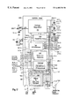
- FIG. 1 shows a schematic block illustration of an apparatus according to the invention in the form of a simulation module in connection with an electronic unit with two-wire bus capability;
- FIG. 2 shows a functional block diagram of a simulation module, forming an offset voltage source Q SG ;
- FIG. 3 shows a schematic circuit diagram of a corresponding module which permits digital setting of an offset voltage V SG ;
- FIG. 4 shows a schematic circuit diagram of an apparatus section which permits digital acquisition of a voltage offset
- FIG. 5 shows a first diagram for illustrating level shifts in terms of transmission and reception, with regard to the single-wire reception capability
- FIG. 6 shows a second diagram for illustrating level shifts in terms of transmission and reception, with regard to the single-wire reception capability
- FIG. 7 shows a graphical illustration of the reception capability of a bus subscriber against ramped potential shifting in the course of performing the method
- FIG. 8 shows an exemplary state diagram of a bus subscriber in the course of performing the method
- FIG. 9 shows an exemplary state diagram in the course of implementing the method of that bus subscriber which performs the steps of “recording phase” (during the test state) and “evaluation phase” (during the evaluation state);
- FIG. 10 shows a schematic illustration of the interruption of the transmission path for the purpose of keeping the bus free from response accesses
- FIG. 11 shows an extract from a block diagram of a circuit or module for illustrating a softwarebased realization of such an interruption
- FIG. 12 shows an illustration of the integration of an apparatus according to the invention in a more complex unit together with a bus transceiver;
- FIG. 13 shows a function block diagram of a power supply which comprises a supply path for providing an auxiliary voltage V T or an auxiliary current I T for the purpose of supporting the inventive apparatus and elements which cooperate therewith in a bus transceiver;
- FIG. 14 shows a simplified block circuit diagram of apparatus elements according to FIG. 12, for example, relating to the transmitting end of the transceiver function;
- FIG. 15 shows a further corresponding block circuit diagram of apparatus elements, relating to the transmitting end of the transceiver function
- FIG. 16 shows a further simplified block circuit diagram of apparatus elements, relating to the transmitting end of the transceiver function
- FIG. 17 shows a further corresponding block circuit diagram of apparatus elements, relating to the transmitting end of the transceiver function
- FIG. 18 shows a schematic illustration of supply sources which correspond to one another or can be converted into one another, and are equivalent in this respect;
- FIG. 19 shows a schematic timing diagram of the source potentials by which signal currents can be dominantly fed from the apparatus onto the bus cores;
- FIG. 20 shows two timing diagrams, superposed on one another, of exemplary signal profiles of the kind that can be generated by means of the apparatus according to FIG. 16 or 17 at core coupling points at the transmitting end;
- FIG. 21 shows a simplified function circuit diagram for illustrating various functionalities of an exemplary apparatus in connection with elements of the transmitting means of a bus transceiver as illustrated in FIG. 12;
- FIG. 22 shows an exemplary logic diagram of the driving functionality L 3 in FIG. 21;
- FIG. 23 shows a simplified function circuit diagram for illustrating further functionalities beyond those of the apparatus according to FIG. 21;
- FIG. 24 shows a distribution diagram of apparatus elements in the sense of FIG. 12, these being limited in this case, for example, to supporting the transmitting end of the bus transceiver 100 ′;
- FIG. 25 shows a function circuit diagram of a developed apparatus which permits, in a simple manner, the direct regulation on the bus core BUS_L of a keying potential to be impressed dominantly thereon;
- FIG. 26 shows a corresponding function circuit diagram for the bus core BUS_H
- FIG. 27 shows a function circuit diagram of a sampler which can be used in the apparatuses according to FIG. 25 and FIG. 26, requires no error compensation and can be integrated very easily, with a hold regulator connected;
- FIG. 28 shows a function circuit diagram of an alternative apparatus which permits direct regulation on the bus core BUS_L of a keying potential to be dominantly impressed thereon and, at the same time, uses an external microcontroller for error compensation, shown in an application in the context of a mobile test unit, for example;
- FIG. 29 shows a modification of the apparatus according to FIG. 28 which, by means of a Sample-&-Hold device, makes it possible to dispense with a microcontroller for the purpose of compensation, applicable to the bus core BUS_L;
- FIG. 30 shows a function circuit diagram of an alternative apparatus for the purpose of feeding onto the bus core BUS_L a source potential having a variable offset with respect to the normal dominant potential;
- FIG. 31 shows a function block diagram of a reception block within a bus transceiver, e.g., in a semiconductor circuit which is equipped with additional apparatus elements;
- FIG. 32 shows a function block diagram of a developed reception block within a bus transceiver in a semiconductor circuit which is equipped with further developed apparatus elements;
- FIG. 33 shows a schematic diagram of part of the apparatus functionality in a reception block according to FIG. 32;
- FIG. 34 shows a block circuit diagram of apparatus elements in accordance with FIG. 12 and FIG. 32 which are restricted to specific applications, relating to the receiving end of the transceiver function;
- FIG. 35 shows a further block circuit diagram of apparatus elements in accordance with FIG. 12 and FIG. 32 which are restricted to specific applications, relating to the receiving end of the transceiver function;
- FIG. 36 shows a further block circuit diagram of apparatus elements in accordance with FIG. 12 and FIG. 32 which are restricted to specific applications, relating to the receiving end of the transceiver function;
- FIG. 37 shows a further block circuit diagram of apparatus elements in accordance with FIG. 12 and FIG. 32 which are restricted to specific applications, relating to the receiving end of the transceiver function;
- FIG. 38 shows a schematic circuit diagram of a development detail of the apparatus according to FIG. 5 for acquiring and transmitting a reference-earth potential difference to a microcontroller;
- FIG. 39 shows a schematic illustration of a central apparatus element which generates all the control signals and value specifications for influencing the transmitting and receiving means of a bus transceiver for the purpose of potential error determination;
- FIG. 40 shows a block diagram for roughly illustrating a unit or module in which a bus transceiver 100 interacts with a microcontroller 21 ;
- FIG. 41 shows a diagram, resolved into function blocks, of a bus transceiver 100 as described in the priority application.
- FIG. 42 shows a diagram, resolved into function blocks, of a bus transceiver 100 ′ as described in the parallel application which was filed at the same time and is cited in the text in connection with FIG. 12 (FIG. 4 in the said parallel application).
- a simulation model 199 A is connected to the normal (dashed) earth (ground) operating current path 218 ′ of a bus subscriber ECU.
- This normal path runs between a subscriber-internal earth busbar SYStem GrouND (SYS GND)—routed to a connection terminal 13 . 1 of the subscriber ECU—and a feeding earth point REMote or REFerence GrouND (REF or REM GND) in the application environment.
- the supply circuit of the subscriber ECU is grounded by the subscriber-internal earth busbar SYS GND via the connections 217 and 218 , which are emphasized in bold, and the simulation module 199 A.
- the operating voltage UBATT is fed to the bus subscriber ECU by a supply busbar (not illustrated).
- the voltage if appropriately reduced to VBATT by a small voltage drop across a polarity reversal protection element 19 , feeds the input 20 . 1 of a voltage regulator 20 .
- the reference point of the voltage regulator is connected to the abovementioned earth busbar SYS GND.
- the earth-side supply terminal of the bus transceiver 100 , 100 ′ to which a stabilized supply voltage VCC of 5 volts, for example, can be fed for the purpose of supplying power from an output 20 . 2 of the regulator 20 . All the remaining electrical components in the subscriber ECU are also connected to the subscriber-internal earth busbar SYS GND.
- the bus transceiver 100 , 100 ′ is connected to a two-wire bus BUS_H/BUS_L, via which the bus subscriber ECU can communicate with corresponding other bus subscribers. It can be equipped for two-wire and single-wire reception. Here, a different response level may be effective in differential two-wire operation (in a wires-specific manner) from that in the case of reception only by the wire respectively under consideration.
- a connection 266 is provided between the bus subscriber ECU and the simulation module 199 A. The connection may also equally exist between the bus transceiver 100 , 100 ′ and the simulation module 199 A. In the event that the simulation module 199 A is part of a mobile test unit, for example, it is also possible to provide a control connection 266 ′, for example, to a computer or the like (not shown here).
- the simulation module 199 A may be constructed in accordance with FIG. 2, for example. Accordingly, the switching path of a switching transistor 199 . 21 of any desired type and a capacitor 199 . 22 may be connected between the terminals 217 and 218 of the said simulation module. Furthermore, a voltage-limiting element 199 . 23 may also be provided in parallel therewith.
- the switching transistor is driven by a potential control apparatus 199 with a PWM signal, for example.
- a potential control apparatus 199 with a PWM signal for example.
- a possibility for feedback of the potential at the terminal 218 into the potential control apparatus 199 is also indicated by a dashed line. Evaluation of this potential enables the latter to be held via a corresponding tracking of the PWM duty ratio independently of the load current I L .
- the potential control apparatus 199 can be driven via the path 266 by a connected ECU or via the path 266 ′, e.g., by a computer in a test unit or the like.
- the simulation module 199 A realizes a controllable voltage source Q SG which is referenced to earth GND and whose terminal voltage can be made to equal zero in the ideal case. This can be effected, for example, via a corresponding continuous driving of the switching transistor 199 . 21 .
- the transistor 199 . 21 is driven by an amplifier 1991 , which is connected by circuitry with resistors R 4 and R 6 as regulator with the transistor 199 . 21 as output stage.
- the non-inverting input of the amplifier 1991 is connected to the terminal 218 and the inverting terminal is connected via the resistor R 6 to the analog output of a D/A converter 199 . 2 .
- the latter can be fed, via a digital path 266 , a specification which then determines the offset voltage V SG that effects a voltage drop across the transistor 199 . 21 and, in this respect, is established between the terminals 218 and 217 .
- the additional apparatus 199 B permits acquisition and digital further processing of a voltage between its terminals 218 and 217 , where an offset voltage V SG may preferably be involved. This is irrespective of how it comes about (present as a real error, or simulated by means of 199 A for the purpose of testing).
- the diagram according to FIG. 5 illustrates the single-wire reception capability when an erroneous earth offset-voltage V SG occurs in a receiver, when the bus level U H dominantly impressed on the bus core BUS_H by a transmitter is reduced in a step-by-step manner by an offset voltage V SH .
- V SH offset voltage
- T 1 to T 4 designate four test states of a transmitter, during which the bus level U H1 to U H4 dominantly impressed on the bus core BUS_H is successively reduced by an offset voltage V SH1 to V SH4 which rises in a step-by-step manner and is referred to the dominant upper voltage of 5.0 volts.
- V SH1 to V SH4 which rises in a step-by-step manner and is referred to the dominant upper voltage of 5.0 volts.
- the receiver having an earth error its Normal state is designated by RN; following this five further states with a monotonically increasing earth offset voltage VSG are designated by R 1 to R 5 ; and finally a steady state with a maximum earth offset voltage of, for example, approximately 2.6 volts is designated by RM.
- the reception window RHTW (in RN 1.5 . . .
- the diagram makes it possible to directly derive the table which is illustrated underneath it and which appertains to the reception possibility when, on the one hand, at the receiver, an earth offset voltage V SG is present and/or rises and the level U H dominantly impressed on the bus core BUS_H is reduced and/or the offset V SH is increased up to the upper voltage of 5 volts. It is evident that with an initially existing reception capability of a receiver subjected to an earth offset, this receiver is the first to lose its reception capability, before all the other receivers, against a successive increase in a transmitter of the offset voltage V SH or reduction in the dominant core voltage U H by this offset voltage.
- the diagram according to FIG. 6 illustrates the single-wire reception capability when an erroneous earth offset-voltage V SG occurs in a receiver, when the bus level U L dominantly impressed on the bus core BUS_L by a transmitter is increased in a step-by-step manner by an offset voltage V SL .
- TN also, denotes the Normal state in a transmitter in the network.
- a tolerance window TWL for the dominant L level from 0.0 to 1.4 volts is specified for example, for this state, where 0.0 volts represents the reference level fixed in a system-specific manner.
- T 1 to T 4 designate test states of a transmitter during which the bus level U L1 to U L4 dominantly impressed on the bus core BUS_L is successively increased to an offset voltage V SL1 to V SL4 which increases in a step-by-step manner.
- the receiver having an earth error, its Normal state is again designated by RN.
- R 1 to R 5 Following this five further states with a monotonically increasing earth offset voltage VSG are designated by R 1 to R 5 .
- a steady state with a maximum earth offset voltage of, for example, approximately 2.0 volts is designated by RM.
- the reception window RLTW (in RN 2.75 . . .
- FIG. 7 illustrates the communications status CST of the data transmission to a bus subscriber having an earth error here, by way of example.
- a simulation voltage V SG which rises in ramped fashion between time markers t 1 and t 4 is illustrated in the right-hand part of the diagram, and the left-hand part of the diagram shows the window that results between time markers t 2 and t 4 and within which it is possible to transmit data to the bus subscriber, or receiver in the latter, having an earth error.
- the method according to the invention makes use of this insight in that it applies universally both under single-wire and under two-wire test conditions.
- particular apparatus elements (compare FIGS. 31-33) within the receivers used in a bus network can enable further reaching evaluations than in the first case.
- the simulation module 199 A must be able to carry the entire operating current I L of the bus subscriber ECU.
- Such a solution is practical when, for example, a perfectly normal bus subscriber with no dedicated apparatus means for carrying out the method is intended to be made suitable and ready for carrying out the method as test subscriber using simple means and without any appreciable interventions.
- the bus subscriber ECU in FIG. 1 is regarded as such a unit, in this respect only the reference point 217 of the correspondingly dimensioned simulation module 199 A according to FIGS. 1-3 is to be connected to the potential REF GND, which serves as a reference throughout the network, and its output 218 is to be connected to the subscriber-internal reference-earth potential busbar SYS GND.
- test subscriber is a perfectly normal bus subscriber which is permanently connected to the bus and, for the purpose of carrying out the method steps, need only be equipped in the sense of FIGS. 10-39, or a correspondingly equipped test unit which is temporarily connected to the bus only for the duration of a test;
- the defective subscriber is in each case that subscriber connected to the bus whose communications capability is actually, or initially only presumably, restricted or lost on account of a reference-earth potential error or communications level error;
- An observational subscriber is each subscriber connected to the bus which can receive a message at least from the test subscriber, but also from the defective subscriber under certain preconditions, but is put into a RECEIVE ONLY status, in a manner governed by the diagnostic program, and is thus prevented from bus access in transmission terms.
- each subscriber has
- a module for handling the bus protocol, of a CAN in the case of the example.
- (c) means and capability of assuming two different operating states in dependence on a control signal EN which can be communicated via the bus, namely the operating states of
- the subscriber functioning as test subscriber is configured in such a way that it:
- (1) is either connected to the known (for example, negative) reference-earth potential in a manner dictated by the construction, or it can detect and take into account a possible inherent potential shift with respect to the abovementioned potential;
- test subscriber needs to have apparatus elements as in FIGS. 13-30 and 34 - 38 .
- all the remaining subscribers that is to say defective subscribers and observational subscribers
- FIGS. 13-38 in respect of their apparatus equipment, since their activation or efficacy is controlled exclusively by software via the bus.
- a mobile “test unit” in the workshop sense
- the method is structured into an “acquisition phase” and a “evaluation phase”. All the subscribers connected to the bus are controlled by the bus subscriber functioning as test subscriber—which, as stated, may also be a temporally connected test unit in the workshop—by means of broadcast data messages.
- This test subscriber installs and alters, with regard to at least one bus core, a dedicated reference-earth potential offset—seen from the bus. Therefore, the test subscriber ultimately installs and alters its respectively corresponding source level to which the bus core is dominantly keyed by the test subscriber (in a predetermined manner), broadcasts data (“stimulus phase”) and then ascertains whether data messages are received by bus subscribers without any errors or with errors (“response phase”).
- the two abovementioned phases can successively alternate one after the other.
- the two abovementioned phases taken together form the acquisition phase.
- the results obtained in the acquisition phase can be evaluated.
- impermissible potential shifts can be assigned to individual subscribers or to groups thereof. All the results obtained are included in this evaluation. This evaluation can be carried out in the test subscriber, but does not have to be. On the other hand, it can equally well be carried out in one or more connected evaluation units.
- the method can be structured into steps as follows:
- a bus subscriber is determined as test subscriber which is capable, physically and with regard to potential errors which are possible in a system-specific manner, of communicating with each of the remaining bus subscribers as potential defective subscriber (that is to say with any system-typical potential error as cause of the potential disturbance of communication under normal conditions);
- test subscriber broadcasts at least one bus message with the purpose of putting all the bus subscribers to be tested into an operating mode “Transmit no application messages”;
- test subscriber broadcasts at least one bus message with the purpose of putting all the bus subscribers to be tested into an operating mode “receive only, transmission not possible” (RECEIVE ONLY), as a result of which these subscribers become observational subscribers;
- test subscriber broadcasts at least one bus message with the purpose of putting, from amongst the number of observational subscribers, a specific subscriber as (potential) defective subscriber into the operating mode “transmit and receive” (NORMAL);
- test subscriber cyclically broadcasts at least one test message
- test subscriber assesses a positive acknowledgement as truth status for the data transmission being free from errors, and a negative acknowledgement or the absence of any acknowledgement as truth status for the data transmission being errored;
- test subscriber shifts at least one source level to which the (at least one) bus core used for testing is dominantly keyed
- the test subscriber records the range of potential shifting of its (at least one) source level in which the test message is received without any errors in accordance with steps 6.a/ and 7/, and the range/s of potential shifting of the (at least one) source level in which the test message is not received or is received with errors in accordance with steps 6.b/ and 6.c/;
- the test subscriber sets a potential shift of the source level dominantly assigned to this bus core into the range in which the test data transmission was previously possible without any errors;
- the test subscriber broadcasts at least one bus message with the purpose of putting the defective subscriber into the operating mode “Receive only—transmission not possible” (RECEIVE ONLY), as a result of which this subscriber again becomes an observational subscriber;
- steps 2/ and 3/ can be interchanged and steps 13/ and 14/ can be interchanged.
- steps 5/ to 9/ can proceed in order or be carried out simultaneously.
- the shifting of the at least one source level in accordance with step 8/ can be carried out in a ramped manner over time, monotonically step-by-step.
- the shifting of the (first) source level in accordance with step 8/ can be carried out alternately with the shifting of a further (second) source level in accordance with a predetermined shifting step pattern.
- the method may furthermore provide a step:
- test subscriber broadcasts at least one bus message with the purpose of putting a bus subscriber which is to be invoked as defective subscriber into an operating mode “subscriber load currents switched on”.
- the method may furthermore provide a step:
- test subscriber broadcasts at least one bus message with the purpose of putting all the bus subscribers into an operating mode “subscriber load currents switched on”.
- potential tests in particular with regard to reference-earth potential shifts dictated by the current consumption, can be carried out only in the defective subscriber given a moderate overall current consumption in the bus network or in all the remaining subscribers (defective subscriber and observational subscribers) given an appropriately high overall current consumption in the bus network.
- the method may furthermore provide a step:
- test subscriber shifts at least one source level to which the (at least one) bus wire used for communication is dominantly keyed.
- the method may further provide for the test subscriber to be a bus subscriber which is permanently connected to the bus and by this bus subscriber at least after each new start-up of the bus network as subordinate to the normal bus operation with regard to all the bus subscribers.
- the method provides for the evaluation results which are to be obtained during the check of all the bus subscribers at least after each start-up of the bus network to be stored in the test subscriber or a bus subscriber which can be selected by the latter.
- the method according to the invention can be implemented in a one-wire or two-wire manner.
- the test subscriber can drive both bus cores for the purpose of testing.
- the method furthermore provides for step 8/ to take place with step 5/ at least at times in a message-interlinked manner step by step and each test message to contain an expectation number from the defective subscriber to be tested.
- the interlinking may advantageously be bit-block-based.
- FIG. 8 illustrates, for example, a state diagram of a subscriber as (potential) defective subscriber which is to be tested under load current conditions in order to be able to identify and determine a possibly impermissibly high voltage drop in its earth line as the disturbing cause of possible communications interference.
- FIG. 9 illustrates, for example, a state diagram of a test subscriber for the simple case of the earth error potential test, from which the division in two into an acquisition phase (during the test state) and an evaluation phase (during the evaluation state) is evident.
- the arrows starting from points designate default inputs of the method in both cases.
- the above-described handling of potential errors in accordance with the method of the present invention at least presupposes that the transmission path between a microcontroller 21 or its bus protocol module 22 and the bus wire connection (single-wire network) or the bus wire connections 11 and 12 (two-wire network) can be interrupted in some way such that the bus can be kept free of undesirable transmission accesses. This is symbolized in FIG. 10 .
- An operating mode RECEIVE ONLY of the bus transceiver 100 , 100 ′ is used for the realization.
- the operating mode is applied by hardware.
- the operating mode RECEIVE ONLY and hence disconnection of the bus from transmission accesses can be effected, for example, from a microcontroller via a control bit EN, which can be transmitted (firstly via the path 166 . 5 and then) via a path 6 to the transmitting means 133 of the bus transceiver. Only when the control bit EN has the prescribed logic level is the bus also available to transmission access by the transceiver, otherwise it is not available. This detail is illustrated for the exemplary case of an SPI implementation in FIG. 11 .
- a (not illustrated) microprocessor or microcontroller communicates with the bus transceiver 100 ′ via the SPI/SCI bus 166 . 5 . Consequently, the EN bit is transmitted here in a logged manner to the bus transceiver 100 ′.
- an EN bit which enables or inhibits the transmitting means 130 or the transmission output stage 133 is generated by decoding, stored and/or overwritten in a control block 140 ′ of a corresponding bus transceiver 100 ′ or 100 . 11 .
- This control block has SPI communications capability.
- the block 142 which sets the operating modes of the transceiver 100 ′ in accordance with an instruction from the microcontroller and which is illustrated there combined with blocks 144 and 145 , is assigned at least one storage register 142 ′.
- This storage register 142 ′ holds the respectively received operating state information until it is overwritten by the reception of more up-to-date information.
- This store also at least comprises a cell for the abovementioned SPI-decoded EN signal for the output stage 133 .
- the path 6 from this store to the transmission output stage 133 within the block 140 ′ is indicated by a dashed line.
- the at least one store for the EN bit is also illustrated in FIG. 37 .
- FIG. 12 illustrates a functional block diagram of a more complex circuit or electronic module 200 .
- a circuit is described in more detail for example, in the application PCT/EP96/05087 which was filed on Mar. 26, 1996.
- PCT/EP96/05087 which was filed on Mar. 26, 1996.
- PCT/EP96/05087 which is hereby incorporated in its entirety.
- what is relevant (essentially) is only the potential influencing means 199 , which are dealt with there for implementation of the method, connected 195 to the bus transceiver 100 , 100 ′ and their digital path via 166 . 5 , 166 , 201 or 201 . 1 to the (not illustrated) microprocessor or microcontroller.
- FIG. 12 illustrates a functional block diagram of a more complex circuit or electronic module 200 .
- FIG. 12 illustrates a functional block diagram of a more complex circuit or electronic module 200 .
- FIG. 12 illustrates a functional block diagram of a more complex circuit or electronic module 200 .
- the potential control apparatus 199 enables a circuit or electronic module 200 which is constructed in such a way or similarly and in any event includes at least one bus transceiver 100 , 100 ′ and identical or similarly acting or utilizable means for communication with a microcontroller 21 to afford (throughout the network) the location, detection and handling of operating level errors and reference-earth potential errors in or at bus subscribers.
- a circuit or electronic module 200 which is constructed in such a way or similarly and in any event includes at least one bus transceiver 100 , 100 ′ and identical or similarly acting or utilizable means for communication with a microcontroller 21 to afford (throughout the network) the location, detection and handling of operating level errors and reference-earth potential errors in or at bus subscribers.
- All the control units of a motor vehicle are mechanically connected to the vehicle body as fixing surface and are directly electrically connected to the vehicle body as reference-earth potential surface (vehicle earth).
- vehicle earth serves, on the one hand, as distribution conductor for closing the operating circuits of loads and control units and, on the other hand, also as reference-earth potential surface for wire bus signals, as in the present case.
- the “offset error” of the earth potential (SYStem GND) internally in the unit relative to the corresponding internal earth potentials of other control units may become impermissibly large.
- the threshold value VREF of the reception discriminators 121 . 2 and 121 . 3 in FIG. 31 are then shifted beyond a bus-specifically permissible tolerance range, and in particular relative to the corresponding threshold values of other bus subscribers.
- the recessive bus level window for this receiver may even be shifted to such an extent that reception is no longer possible.
- the purpose of the apparatus according to the invention is to impart to a corresponding bus system (line network and subscribers) not only the capability of locating and verifying such defective bus subscribers but also the capability of latent testing and monitoring of the operating level windows of all the subscribers.
- a measure which describes the margin that presently exists for one or more bus subscribers in each case before it or they undergo failure caused by a level error (in addition to other aspects, this measure is the most important one with regard to defining the bus quality).
- a service station during each service, can thus immediately obtain an impression of the overall state of the physical-communicative matching of the transceivers in the bus network with regard to one another and, if necessary, carry out precautionary or maintenance work in a highly targeted manner with minimum outlay. It is evident that in a motor vehicle having a very large number of such circuits in very many control units connected to the vehicle earth, intervention possibilities which are supported in this way, before the actual occurrence of the error situation, avoid unnecessary service outlay and increase the availability of the motor vehicle.
- a (semiconductor) circuit is discussed under the designation 200 , for the sake of simplicity.
- a conventionally produced electronic module with comparable or similar functionalities may also equally well be involved in this case, without thereby leaving the scope of the invention.
- such a circuit or such a module may also be, within the scope of the invention, part of a specific bus test unit.
- SPI Serial Parallel Interface
- FIGS. 46 - 52 Further apparatus elements are also provided in the receiving section 120 (not presented in the figures in this case) for maximum testing flexibility (FIGS. 46 - 52 ). These elements and the way in which they can be realized, for example, without restricting the generality in order to interact with the potential control apparatus 199 , will be described below.
- the potential control apparatus 199 (OFFSET & BUS TEST MANAGER) can be connected, for example, via a particular terminal 13 . 1 to a reference-earth point SYSTEM GND in the unit carrying the circuit 200 . Furthermore, the potential control apparatus 199 can additionally be fed (preferably, via an upstream apparatus element 198 (SENSE/EMI PROTECTION)) an external reference-earth potential REMote GND from the application environment of the relevant unit via another particular terminal 13 . 2 .
- the line 196 in any event, symbolizes a connection which (in the abovementioned example of a vehicle) can be routed from the relevant unit to an earth point on the vehicle body. This earth point is essentially free from current loading.
- the potential control apparatus 199 is operatively connected to the transceiver 100 , 100 ′ in a manner of greater or lesser complexity, which is intended to be symbolized by the multiple path 195 . Attention is already drawn at this point to the fact that this complexity may result from the fact that the potential control apparatus 199 (for instance, in a semiconductor circuit) may be connected to a greater or lesser extent to control structures of the transceiver 100 , 100 ′ (comprising receiver and/or transmitter) and/or the SPI interface 166 , which establishes a connection to a microcontroller 21 , for example, or may even be properly embedded in such structures.
- the latter may be supplied with power from the potential VCCA from the output 20 . 2 . 2 of the block 20 A.
- this is a voltage regulator, for example. Attention is expressly drawn to the fact that the invention is in no way bound to the presence of power supply parts together with the bus transceiver 100 , 100 ′ in one and the same circuit or electronic module 100 ; the combination made here has only a non-restrictive exemplary character.
- the voltage regulation 20 may optionally comprise, in addition, at least one third regulator 20 T for a further supply potential V T or else a fixed supply current I T , as illustrated in FIG. 13, from which the potential control apparatus 199 (and also the bus transceiver 100 , 100 ′, if required) can be supplied via a feeding path 197 . That is to say supplied with a high degree of decoupling with respect to the output 20 . 2 . 2 of the regulator 20 A having the potential VCC A .
- the voltage V T will be higher than the voltage VCC A , depending on the realization of the potential control apparatus 199 and on the degree to which different features are formed (for example single-wire or two-wire testing capability, small- or large-swing level testing capability, etc.) and the production technology of the elements 100 , 100 ′ and 199 .
- the terminal 20 . 2 . 3 shown in FIG. 12 can, in this respect, be provided (only) for the connection of a filter capacitor 161 . 3 , that is to say not for supplying other circuits or unit components, or for external monitoring purposes, particularly if a current source output is involved, for example. As is evident from FIG.
- the block 20 T may also be designed in such a way that its output quantity can be changed over between a voltage V T and an impressed current I T , in this case, for example, under control access via the SPI path 166 . 5 .
- Such a design in interaction with circuit structures in the potential control apparatus 199 and in the bus transceiver 100 , 100 ′, can effect, inter alia, the automatic changeover or switching on and off of the functions of such structures.
- the potential control apparatus 199 only comprises means which allow the so-called dominant level window at least of the output stage 133 of the transceiver 100 , 100 ′ to be influenced, in particular to be increased, with regard to a reference potential.
- FIG. 14 This is illustrated in FIG. 14 .
- a D/A converter which is also incorporated in 199 and is driven via the digital path 166 . 5 is provided for the specification of a voltage value which acts on a controllable offset voltage source Q SG . This effectively appears looped into the current path of the “normal” earth connection of the output stage 133 to the potential GND, which is also possible in the case of integration by suitable monolithic insulation of diverse components of the output stage 133 .
- a voltage clamp or a voltage regulator CD is connected in parallel with the said output stage.
- the output stage can preferably be supplied with power via a current source CS from a supply busbar at a correspondingly high potential VBATT or V T , and from the regulator CD in the second case, in which case the regulator CD can then be fed by the said supply busbar via the supply path SUPPLY indicated by a dashed line.
- the current source CS can also be entirely omitted if it is possible to supply the output stage 133 by means of an impressed current I T from the regulator 20 T in accordance with FIG. 13 .
- the controlled voltage source Q SG can be realized by an impedance converter which converts the output voltage swing of the D/A converter 199 . 2 in a ratio of essentially 1:1 to a source impedance which is appropriate to the feeding current of the output stage 133 .
- a potential control apparatus 199 configured in this way, in conjunction with a correspondingly equipped transmission output stage 133 , thus permits an error voltage to be simulated at the transmitting end by means of digital setting data which are obtained via the path 166 . 5 .
- the error voltage in the case of a bus transceiver, no longer allows normal communication, in particular normal reception, in a bus subscriber with an earth error.
- the error voltage in the case of the receiver subjected to reception interference can thus be compensated for, at least partly or completely, across the entire bus termination (i.e., terminating load of all the remaining subscribers and, if appropriate, an additional error load).
- the terminal voltage of the source Q SG is expediently adjustable in a defined manner, in particular can be altered at least in steps, that is to say, given a corresponding stepped nature (for example, in staircase or ramped fashion to a greater or lesser extent) over time in accordance with respective specifications via the digital path 166 . 5 .
- the apparatus may equally well comprise two separate controllable offset voltage sources Q SL and Q SH , the source Q SL corresponding to that described above.
- the source Q SH is connected in such a way that it permits a correspondingly digitally controllable alteration of the positive supply potential VCC or VBATT or V T of the core output stage 133 H. In this case, therefore, the L source level feeding onto the bus can be altered independently of the H source level feeding onto the bus, and vice versa.
- controllable offset source Q SL may sweep across a voltage swing of 0 to 3 volts and the controllable offset source Q SH one of 8 or 3 to 0 volts.
- the controllable offset source Q SH may adjust the dominant L source level from 0 to 3 volts and the dominant H source level from 3 or 8 to 0 volts.
- an offset voltage source Q SH adjustable between 0 and 3 volts underneath a supply busbar VCC, with 5 volts being equivalent to an adjustable offset voltage source Q VCC , across GND with an adjusting range from 5 to 2 volts.
- the invention covers the apparatus according to FIG. 15 to the effect, on the one hand, that the two offset sources Q SL and Q SH can be utilized alternatively, as is illustrated in somewhat more detail in FIG. 21, FIG. 22 and FIG. 24, for example, without restricting the generality.
- the two offset sources Q SL and Q SH can be utilized alternatively, as is illustrated in somewhat more detail in FIG. 21, FIG. 22 and FIG. 24, for example, without restricting the generality.
- in principle in each case only one voltage specification is ever necessary. Furthermore, in this respect, only one D/A converter which can be correspondingly charged/recharged during the selection from both alternatives of the specification that is currently required in each case is necessary.
- the invention equally covers the apparatus according to FIG. 15 to the effect that the two offset sources Q SL and Q SH can be utilized simultaneously and independently of one another, as is illustrated in somewhat more detail, for example in FIG. 23, without restricting the generality.
- the three figures mentioned will also be referred to further below.
- the apparatus according to FIG. 16 also allows the installation of at least two offset sources Q SL and Q SH which can be utilized simultaneously, a D/A converter 199 . 2 having two corresponding outputs for the specification of two offset values being provided in that figure.
- one output is fixedly assigned to the source Q SL and the other output is provided exclusively for the optional control of a first source Q SH (on the supply busbar V T or VCC) and of a second source Q SHH (on the higher-potential supply busbar VBATT or V T ).
- logic driving of both output stages by means of at least one impressed current path is provided in this case as well.
- the digital path 166 . 5 driving the D/A converter 199 . 2 furthermore drives a logic arrangement 199 . 5 , which, for its part, is both connected to the D/A converter 199 . 2 and triggers a flip-flop 199 . 6 .
- the two mutually inverted outputs of the flip-flop 199 . 6 drive the offset sources Q SH and Q SHH in the sense of a selection.
- an active ENAble signal is applied to one or the other offset source, that is to say either the offset source Q SH on the supply busbar V T or VCC or the offset source Q SHH on the (still more positive) supply busbar VBATT or V T is active (that is never both simultaneously).
- each of the offset sources Q SH and Q SHH may be thought of as a short circuit (or, in practice, as a source having an insignificant residual voltage drop).
- the logic arrangement 199 . 5 may thus be configured in such a way that in the event of the flip-flop 199 . 6 being triggered, for the purpose of a state change, the logic arrangement can also drive the D/A converter 199 . 2 for the purpose of recharging at least of one desired value specification (in particular, in the sense of a selection for the source Q SH or Q SHH ).
- the voltage ranges entered in FIG. 16 are self-explanatory.
- This apparatus thus permits a dominant H source potential which can optionally lie below or above the bus-specifically normal H source potential or equally well be keyed, as required, between both. It furthermore lies within the scope of the invention to design the logic arrangement 199 . 5 appropriately so that such a changeover is also enabled in a manner interlinked with the data signal TxD, this being symbolized by the dashed signal path to the logic arrangement 199 . 5 .
- the apparatuses that have been described up to this point thus make it possible to shift one or both feeding dominant source level/s, on the one hand, in a direction in which the reception level window of a bus subscriber is also necessarily shifted when it has a defective connection to a reference-earth potential.
- This resultant connection carries current and, in this respect, causes its own offset voltage drop, such as, for example, in the case of a defective earth connection of a control unit as bus subscriber to the body of a motor vehicle.
- a D/A converter 199 . 2 which permits the outputting of in this case, for example, three analog control or desired values to corresponding offset sources Q SL , Q SH and Q SHH . Without restricting the generality, all or only two of these values can be available simultaneously.
- the D/A converter 199 . 2 can be driven via a digital path 166 . 5 of the SPI type, for example.
- a logic arrangement 199 . 7 can likewise be driven by the digital path 166 . 5 and interacts with the D/A converter 199 . 2 via a bidirectional connection 199 . 8 .
- the logic arrangement 199 . 7 can be driven by the SPI clock signal; the supply of an external time base signal may also equally well be provided.
- a corresponding time base signal could be derived by a timer within the circuit 200 —in this case, for example, by a so-called wake-up expander 165 ′. If the wake-up expander 165 ′ is (for its part) supplied, according to FIG. 12, the signal can be derived with a time or frequency signal (for instance via 164 a from a watchdog function 164 ), could either be temporally interlinked with a period of an internal reference signal of the watchdog function 164 or obtained from a branch of the connection 164 a in FIG. 12 .
- the transmission signal TxD may also be fed to the logic arrangement 199 . 7 .
- the output stages 133 L and 133 H are driven by the logic arrangement 199 . 7 via respectively individual logic paths with current impressing.
- a measurement amplifier 199 . 8 which is wired to generate a quantity corresponding to the difference between the earth potential internally in the chip or unit and an external reference earth REM GND. This quantity can be fed in this case to the D/A converter 199 . 2 , for example.
- the configuration and function of the logic arrangement 199 . 7 in connection with the D/A converter 199 . 2 are as follows.
- the logic arrangement 199 . 7 Driven by a clock signal, which may either be the clock signal of the path 166 . 5 or else one which is obtained in accordance with the description above, the logic arrangement 199 . 7 generates, inter alia, in accordance with data received via the path 166 . 5 , control signals for the D/A converter 199 . 2 . These signals enable the D/A converter to generate and provide desired value specifications of the A/D converter which alter in a defined manner in ramped fashion, and/or to freely alter the dominant window width in a defined manner (squeezing of the bus bit eye width) and also to effect the selection or changeover (ENAbling) of the corresponding target offset source(s) Q SL , Q SH and/or Q SHH
- the first function can be carried out both for single-wire and for two-wire tests and the second function (so-called “squeezing”) can preferably be provided for two-wire tests.
- the second function can preferably be provided for two-wire tests.
- analog voltage levels which approximate a voltage ramp or represent a squeeze increment or decrement, if necessary is optionally time-slot-interlinked with the (not necessarily) synchronous data signal TxD.
- a ramp increment or decrement to be effected at the earliest or exactly after a number of transmission bit periods.
- This number is determined by the number M. If this number M can be received by all the bus subscribers with reception capability, test software which is correspondingly designed can convey, using this predeterminable number M, virtually elementary verification foreknowledge regarding an imminent test cycle throughout the bus.
- the apparatus can also comprise (in addition) means which are not illustrated in the figures and enable a current reference changeover of the output stage 133 H between the offset sources Q SH and Q SHH to be effected within a period of time which is shorter than the bus bit period.
- FIG. 20 illustrates an enlargement at the bit plane when the abovementioned feature of enabling a changeover of the current reference of the output stage 133 H between the offset sources Q SH and Q SHH is possible within a time shorter than the bus bit period. It is evident from this that current feeding into a bus core is not possible under certain preconditions, something which can be utilized for discrimination purposes.
- FIGS. 21-23 convey a number of practical examples in this sense, using simplified circuit diagrams, in order to make the different functionalities plausible. In this regard, they do not constitute any restriction at all to the invention. Rather, for example, depending on the realization technology in a circuit or module, it is also possible to realize circuit diagrams which are very different from these. This is in order to achieve in practice the functionality which is illustrated.
- FIG. 21 shows a circuit diagram in which are assembled elements that can be assigned both to the potential control apparatus 199 and to the bus transceiver 100 , 100 ′ (in particular to the output stage 133 thereof).
- this exemplary embodiment of a potential control apparatus and cooperating apparatus elements in the bus transceiver approximately conveys the functionality of what is illustrated in the block diagram in FIG. 16 .
- the collectors of the transistors 1303 and 1304 feed the bus cores BUS_L and BUS_H, respectively, via protective diodes DL and DH, respectively. Furthermore, if appropriate, the collectors feed the bus cores via small protective resistors RL and RH, respectively.
- the transistors 1301 and 1302 fulfil, in alternation with one another, an overall triple function, for which purpose they can be driven, on the input side, via analog changeover switches S 1 and S 2 which can be controlled by digital signals S 1 and S 2 .
- the transistor 1301 is firstly held at saturation by the current source 1994 feeding from the potential V T , as a result of which the emitter of the transistor 1303 is almost at earth potential GND.
- the resistor R 2 of the voltage divider formed by R 1 and R 2 is, secondly, also connected to GND, with the result that the said voltage divider has the division ratio R 2 / (R 1 +R 2 ).
- switch S 2 in position to the base of the transistor 1302 is connected to the output of the regulator 1991 .
- the transistor 1302 in conjunction with the regulator 1991 , functions as output stage of an offset source Q SH .
- the regulator 1991 can be constructed in a known manner. Under certain conditions, it may also be based on a comparator 1992 , as assumed in the example.
- the capacitor C 4 indicated by way of example, in conjunction with R 5 and R 6 are then to be matched, if appropriate, in accordance with technical regulation requirements to a non-ideal phase-shifting behaviour of the transistors 1301 and 1302 .
- Other compensation means may also be expedient, depending on the properties of the comparator.
- the capacitors 1308 and 1309 which can be used for EMC protection purposes may in turn be advantageous in a differently configured regulator.
- An analog desired value specification of the D/A converter 199 . 2 is fed to the regulator 1991 . Since the regulating circuit is closed via the transistor 1302 and the abovementioned voltage divider formed by R 1 and R 2 , the DC voltage present at the emitter of the transistor 1304 can be regulated as offset voltage which decreases the potential VCC A (source Q SH ).
- the selection logic arrangement L 3 drives a further analog changeover switch S 3 with a signal S 3 .
- this changeover switch it is possible to change over the output of the regulator 1991 , given truth of the high bit HB, from the transistor 1302 to the transistor 1996 which is fed from the more positive supply busbar V T . In this case, the transistor 1302 is then inactive.
- the diode 1998 is expedient depending on the technology. A zener breakdown of the transistor 1302 when the transistor 1996 is near saturation can be ruled out in the case of realization using high-voltage technology in the event of relevant differences between V T and VCC A .
- the D/A converter 199 . 2 is driven by a logic arrangement 199 . 1 , which is in turn driven via the digital path 166 . 5 .
- the logic arrangement 199 . 1 has the function of an interface to the digital path 166 . 5 and, in this respect, may comprise at least one register in which at least part of a data telegram that is received serially can be held temporarily.
- the flip-flop illustrated in FIG. 16 is contained therein as storage cell. For example, a bit line HB (for High Bit) leading to the D/A converter and also two further bit lines N (for Normal or Override) and SS (for Shift Select) are routed to the selection logic arrangement L 3 (the override function is explained in the next paragraph).
- An exemplary realization of this aim is reproduced in FIG. 22; it is configured in dependence on the truth evaluation of its input signals.
- the abovementioned override function is as follows: given a truth state of the signal N, the operating state of the output stage is activated for normal bus communication, irrespective of whether HB driving is simultaneously effected or which of the two dominant source potentials GND and VCC A is selected for “manipulation” by offset shifting in accordance with the D/A converter.
- Another driving path leads from the logic arrangement 199 . 1 to a further analog changeover switch S 4 , via which the earth terminal of the D/A converter 199 . 2 and of the regulator 1991 can be connected optionally to, for example, the potential Chip GND or the terminal 13 . 2 for the external reference-earth potential REM GND, in dependence on a control signal S 4 (ReFerence) from the logic arrangement 199 . 1 .
- a control signal S 4 ReFerence
- a functionality in accordance with this exemplary embodiment already covers a large number of potential tests which can be executed in a single-wire manner and require, at an instant, in each case offset influencing only of one feeding dominant source level.
- the apparatus according to FIG. 23 constitutes an expansion for applications in which simultaneous offset influencing of both feeding dominant source levels is necessary.
- This exemplary apparatus also constitutes no restriction at all to the invention and serves only for illustrating the functionality.
- two separate regulators 1991 H and 1991 L are provided and an undivided acquisition (enabled by auxiliary current sources 1312 and 1313 ) of the actual offsets at the collectors of the transistors 1301 and 1302 .
- the corresponding logic arrangement 199 . 1 is provided with an additional output WM (Wire Mode).
- the corresponding logic arrangement L 4 may be designed similarly to the logic arrangement L 3 .
- a two-channel hold device 2001 with signal supports 2002 and 2003 which is driven by the interface logic arrangement 199 . 1 via two additional connections (Channel and Strobe).
- the two-channel hold device 2001 with its two outputs 2004 and 2005 feeds the desired value inputs of the regulators 1991 L and 1991 H.
- a separate emitter pitch 2000 L of the transistor 1301 and a sampling line 2000 H at the diode 1998 are provided.
- quantities which can be picked off therefrom can be incorporated into overload disconnection for instance of the voltage regulators 20 U and 20 A in accordance with FIG. 13 .
- This example illustrates, in a schematic simplification, the distribution of exemplary elements of a solution in accordance with FIG. 15 for the case of two offset sources Q SL and Q SH which cannot be utilized simultaneously and for the special case where the feeding dominant H potential need not be greater than VCC A .
- the elements which effect potential shifting namely, the transistors 1301 and 1302
- the elements which effect potential shifting can expediently be integrated without difficulty as components of a thermally equilibrated transmission output stage.
- identification therefore, they are also assigned to the transmission output stage in this case.
- This apparatus example also serves exclusively to illustrate the resolution or distribution in which apparatus components can be constructed, and does not represent any restriction at all to the invention.
- the following apparatuses are aimed at applications in which, by contrast, a maximally direct and, in this respect, more accurate definition of a core voltage (that is voltage impressing) is desirable for the sake of testing.
- the example according to FIG. 25 relates to a corresponding potential specification onto the core BUS_L and the example according to FIG. 26 onto the core BUS_H.
- essential elements are illustrated in an implementation which is possible, for example.
- elements are omitted which prevent regulation when, for example, potential conditions are present which do not allow energization of a bus core under an offset.
- mutually corresponding parts of the functionality could be attributed to the potential control apparatus 199 , they are distinguished from one another in a core-specific manner by the letters L or H also.
- An essential element common to both apparatuses is a Sample & Hold circuit 2010 L and 2010 H connected between supply terminals GND and, for example, V T or VBATT.
- the Sample & Hold circuit has an input which, for example, is directly connected to the bus core BUS_L and BUS_H, respectively. Furthermore, a pulse-triggering circuit 2011 L and 2011 H, respectively, is provided. This circuit is edge-triggered, preferably by the data signal TxD, and generates a very short sampling pulse SP.
- the sampling pulse SP follows the arrowed clock edge within the data bit period and, for example, proceeds towards GND in the first case and towards V T or VBATT in the second case.
- the expedient polarity depends on the technology of the sampler used.
- the Sample & Hold circuit 2010 L and 2010 H additionally comprises a holding element and, if necessary, also impedance conversion means according to the prior art from the output side.
- the transistor 1303 and 1304 is already switched on by the respectively effective active edge of the data signal TxD when the sampling pulse is triggered (positive masking).
- the regulating circuit from the output of the controllable offset source QSL and QSH, respectively, via the output stage transistor 1301 and 1302 , respectively, and also the diode DL and DH, respectively, and the protective resistor DL and DH, respectively, as far as the input of the Sample & Hold circuit is closed a short time later. This occurs at the instant of sampling via the switched-on transistor 1303 and 1304 , respectively.
- the sampled variable output by the Sample & Hold circuit 2010 L and 2010 H, respectively, and the desired value specification from the D/A converter 199 . 2 L and 199 . 2 H, respectively, are fed via connections to the offset source Q SL and Q SH , respectively, for the purpose of setting the latter.
- the offset source Q SL and Q SH By means of an ENA and an NENA signal at the activation input of the pulse-triggering circuit 2011 L and 2011 H, respectively, and a deactivation input of the offset source Q SL and Q SH , respectively, the latter can be driven to obtain a short circuit with respect to earth GND, respectively, and with respect to the busbar V T or VBATT and the sampling pulse generation in 2011 L and 2011 H, respectively, can be inhibited. In this state, the affected offset source Q SL or Q SH is then inactive.
- the apparatus according to FIG. 26 can, as already shown above, also be extended to two corresponding sources Q SH and Q SHH , or else it is possible to provide a backup supply source Q VCC , that replaces these. It is also possible to design both examples for optionally alternate or simultaneous operability.
- FIG. 27 illustrates a sampler 2015 which is suitable for this purpose which can be realized in a particularly simple and accurate manner monolithically, for example.
- the sampler 2015 is wired for the bus core BUS_H.
- the sampler preferably uses a complementary-balanced current source structure 2014 , sample-pulsed at the input 2016 , in the 20 / 9 pitch design as well as a sampling diode DS 1 , connected 2018 to the bus core BUS_H, and a compensation diode DS 2 connected to the input of a holding regulator 199 H.
- This compensation diode D 52 has an impressed, mandatory forward current ratio of 0.55 to 0.45. Since the required current I S is very small, and is actually sampled only in the test mode and corresponding controlled current source structures 2015 can be designed monolithically with a low intrinsic current consumption, special driving arrangements and/or current enabling means for power-saving purposes are superfluous.
- the sampling diode DS 1 fulfils an important protection function for the downstream-connected regulator in the event of a short circuit with respect to the potential UBATT or the application of an even higher interference voltage to the bus core BUS_H.
- the sampling voltage at the output 2017 is near to the actual core voltage U BUS — H when the output stage transistor 1304 is in the on state.
- the residual error smaller than the practical resolution gradation of D/A converters 199 . 2 of relevance (in this case) is obviated.
- the current source structure 2014 including the two diode paths DS 1 and DS 2 , can be integrated to be small, of low capacitance and balanced with respect to a sampling nucleus 2015 which has only two further terminals 2016 and 2017 in addition to terminals VBATT or V T and GND for its power supply and the bus core node 2018 .
- a sampling nucleus 2015 which has only two further terminals 2016 and 2017 in addition to terminals VBATT or V T and GND for its power supply and the bus core node 2018 .
- This apparatus element is advantageous, therefore, insofar as although an unavoidable error voltage is also produced in this case, it is, on the other hand, compensated for at the same location and in the same monolithic structure in which it is necessarily caused. This occurs while it utilizes exactly the same physical principle of action underlying its genesis.
- Thermal invariance of the error compensation also follows from this, which thermal invariance can be realized within wide limits. For these reasons, it is possible to dispense with any compensation assistance, for instance, from the circuit 200 or even loading an external microcontroller 21 for the purpose of computational compensation.
- the apparatus according to FIG. 28 fulfils an entirely different application, in which a powerful microcontroller cooperates with the circuit 200 , the utilization of its computing power and corresponding utilization of the digital path 166 . 5 , 201 . 1 do not have a disturbing consequence or it is not possible to realize a sampler which affords protection in the sense above and has physical error voltage compensation, as shown in FIG. 27 or the like.
- the actual core output stage 133 L is utilized not for the purpose of feeding in the desired core potential but rather only as a driver stage for driving a backup switch 2019 which affords backup feeding and, for its part, is connected to the bus core BUS_L by a separate protective diode DL′.
- the current flowing away into the bus from the dominant feeding potential therefore takes an entirely different route in this case, namely from the regulating point RP at the output of the core potential regulator l 991 L via the switching path of the transistor 2019 and the protective diode DL′.
- a low-resistance changeover switch SWL is provided which can be activated into the switching state shown for the duration of corresponding potential tests.
- a D/A converter 199 . 2 L supplies the regulator 1991 L with a desired value for the voltage to be set at the regulating point RP.
- the error voltage U ERR dropped across the elements 2019 and DL′ due to the flow of current is detected by a further amplifier 2023 , which is wired up to form a measurement amplifier 1991 EL, and the corresponding analog output voltage U Diff is fed to an A/D input of a microcontroller 21 (not illustrated here in the figures).
- the microcontroller 21 can thus calculate the value of the bus core voltage from the digitally converted error voltage U Diff and the present digital desired value specification for the D/A converter 199 . 2 , at a resolution which is predetermined by the stepped nature of the D/A converter 199 . 2 L.
- the regulator 1991 L preferably realizes, in conjunction with the compensation of the error voltage U ERR with regard to the bus core BUS_L, a current-limited voltage source having a maximum current of 200 mA, the feeding source voltage breaking down when the said maximum current is reached.
- terminal 2022 for the analog output of the amplifier 2023 further terminals 2020 and 2021 are required on the circuit 200 when the changeover switch SWL is realized outside the circuit or module 200 .
- the apparatus may also be accommodated in the periphery 500 remote from the bus transceiver 100 , 100 ′ in a, for example, mobile test unit which is connected to the bus only for test purposes.
- the changeover switch SWL can then be located in the said test unit, for example.
- the parts within the border PG are located in a mobile test unit which can be connected between an electronic module 200 with bus capability, in this case, for example, situated in a control unit ECU, and a bus wire BUS_L or CAN_L.
- a bridge B may be removed in the connection region of the unit ECU, with the result that the terminating resistor 17 , which is normally connected to the bus line BUS_L via this bridge, can be connected via a contact TL to the said bus core in the test unit.
- the output of the output stage 133 L can be connected via a further contact EL to the control input of the backup switch 2019 in the test unit PG.
- the bus wire is connected via a further contact BL to the test unit.
- the compensation path then preferably runs via the microcontroller of the test unit.
- An apparatus for corresponding connection to the bus core BUS_H would largely correspond to that described above.
- the apparatus according to FIG. 29 avoids the terminal 2022 and the compensation path via the microcontroller in that, by means of a Sample & Hold circuit 2010 L′, it samples and holds the abovementioned output voltage of the measurement amplifier 1991 EL rather than the core voltage U BUS — L.
- a sampling pulse SP which (interlinked with the data signal TxD) is generated after the active edge of the latter is applied to the said Sample & Hold circuit by a pulse-triggering circuit 2011 L′. Without restricting the generality of the invention, this may be an edge-triggered monostable multivibrator STMF.
- the error quantity which corresponds to the error voltage U ERR and is held by 2010 L′ is fed forward to the core potential regulator 1991 L as interference quantity and accounted in analog form.
- a core voltage U BUS — L corresponding to the quantity which is predetermined on the digital path 166 . 5 is obtained as a sum of the regulator output voltage U a and the respective error voltage U ERR .
- FIG. 31 illustrates, for example, a reception block 120 ′ as part of the transceiver 100 / 100 ′ not only for reception purposes but also for verification of communications errors.
- a reception block 120 ′ is another example as a consequence of reference-earth potential errors of the electronic unit containing this reception block, in conjunction with previously described functionalities of the potential control apparatus 199 and cooperative level-shifting features of the output stage 133 in the transceiver 100 / 100 ′.
- the reception block 120 ′ comprises a front end 121 of analog action, a digital evaluation logic arrangement 128 and a read-out and control logic arrangement 129 .
- the front end (LEVEL DISCRIMINATING SECTION) comprises three level discriminators 121 . 1 to 121 . 3 of analog action. These discriminators are preferably designed as comparators and generate, by analog comparison of the bus line levels with regard to one another and also to a reference potential VREF, signal levels and edges which can be further digitally processed.
- the evaluation logic arrangement contains a circuit function 122 ′.
- the serial bus information RxD as digitally normalized bit stream is recovered from the defined signal levels and edges.
- bus errors in a line core-dependant manner are identified.
- the circuit function 122 ′ is also designed for single-wire reception (across GND).
- the evaluation logic arrangement 128 may comprise digital circuit functions 123 H and 123 L as apparatus components. These circuit functions permit an error signal which is respectively indicative of the assigned bus core BUS_H/CAN_H or BUS_L/CAN_L to be output when a presettable number of directly or actually successive bit errors is reached or exceeded (bit error depth discriminator or bit error accumulation discriminator).
- the circuit functions 123 H and 123 L are multiply connected to the circuit function 122 ′.
- the read-out and control logic arrangement comprises a functionality which is combined to form a control interface 124 and, at least partially, may also be part of the digital SPI interface 166 or be combined therewith. Additionally, they may also be part of preferably at least two storage cells 127 H and 127 L with set inputs 127 H 1 and 127 L 1 , respectively, reset inputs 127 H 2 and 127 L 2 , respectively, and state outputs 127 H 3 and 127 L 3 , respectively.
- These elements which are not used for normal reception, are also to be attributed in the broader sense to the apparatus according to the invention and, within the circuit or module 200 , may also be part of a larger error memory or register, for instance in connection with an EEPROM.
- the reset inputs 127 H 2 and 127 L 2 and also the state outputs 127 H 3 and 127 L 3 of the discrete storage cells 127 H and 127 L are connected to the control interface 124 / 166 .
- An error signal can be applied to the set input 127 H 1 from the circuit function 123 H.
- An error signal can be applied to the set input 127 L 1 from the circuit function 123 L.
- Connections 126 H and 126 L enable setting information with regard to the bit error depth to be discriminated and with regard to the bit error number to be accumulated as well as to the selection of these two methods of discrimination to be transferred from the control interface 124 / 166 to the circuit functions 123 H to 123 L, respectively.
- Connections 125 enable setting information to be transferred from the control interface 124 / 166 to the circuit function 122 ′, which may also contain, inter alia, at least one storage or shift and/or counting register.
- control interface may furthermore be operatively connected to means 170 . 2 for slew rate influencing in the front end 121 and in the evaluation logic arrangement 128 and is then preferably also capable of communication via the SPI bus 166 . 5 with the surroundings of the reception block 120 ′.
- these further means 170 . 2 may likewise be attributed in the broader sense to the apparatus according to the invention.
- the slew rate influencing can assist analyses of core-specific bit errors both in interaction with the previously described functionalities of the potential control apparatus 199 and the cooperative level-shifting features of the output stage 133 in the transceiver 100 , 100 ′ and in the event of capacitive disturbances in the bus network and also in the event of communications interference on account of electromagnetic interference effects on the bus network or a bus subscriber.
- a reception block 120 ′ of a bus transceiver 100 ′ that is augmented by the abovementioned apparatus elements can support, in addition to its normal bus reception function under suitable network management software, in a bus line-specific manner, error analyses under SPI control.
- this reception block 120 ′ can expand the overall functionality of the circuit 200 , namely in respect of monitoring and diagnosis functions with regard to the determination of bus subscribers with reference-earth-potential-error-based communications interference, also under two-wire test conditions, in conjunction with associated transmitting means as “passive responder”.
- reception block in conjunction with a potential control apparatus 199 , can be understood and operated as part of a test system resolved throughout the bus, which last relies, in terms of hardware, at least on a plurality of correspondingly equipped bus subscribers.
- reception block 120 ′ with regard to augmentations which cooperate with the potential control apparatus 199 , can also be structured differently in its sections 128 and 129 or at those locations comprise function blocks which differ from the present exemplary embodiment, in order overall to realize the discrimination features described.
- a reception block 120 ′′ which is augmented by further apparatus elements in accordance with FIG. 32 .
- it affords a normal two-wire and single-wire reception function.
- suitable diagnostic software it supports, in conjunction with functionalities of a more complex potential control apparatus 199 ′, which is in this case assigned to this block 120 ′′, for example, and the above-described level-shifting features of the output stage 133 , analyses of reference-earth potential errors, bus levels and bus windows, in conjunction with associated transmitting means as “active responder”.
- Receivers augmented in terms of apparatus in such a way can advantageously be utilized, under a network diagnostic program, as potential and signal-agile observers with measuring probe function actively for the purpose of (latent) network quality monitoring. It is preferably designed using integrated technology.
- the reception block 120 ′′ likewise comprises a level detection section 121 A of analog action, a threshold value specification and shift section 121 B, a logic current coupling section 121 C, a digital evaluation logic arrangement 128 A and the said potential control apparatus 199 ′, which in this case has a functionality which is pitched further than in the case of offset influencing only at the transmitting end.
- the level detection section (LEVEL DISCRIMINATING SECTION) comprises three level discriminators 121 . 1 to 121 . 3 of analog action. These are preferably designed as comparators.
- the comparator 121 . 1 generates a first digital output signal by comparing the two bus-line levels with reference to one another.
- the comparator 121 . 2 generates a second digital output signal by comparing the level of the bus core BUS_H/CAN_H with a first threshold value voltage VT H of a first threshold value source 121 . 4 .
- the comparator 121 . 3 generates a third digital output signal by comparing the level of the bus core BUS_L/CAN_L with a second threshold value voltage VT L of a second threshold value source 121 . 5 . All three comparators generate signal levels and edges which can be further processed digitally.
- the discriminators 121 . 1 to 121 . 3 are constructed in such a way that they are electrically “raised” together with their respective supply terminals of lower and higher potential relative to the chip substrate, that is to say they can “float”. This is ensured by a particular monolithic construction and insulation in the structure of the semiconductor chip and also by the fact that their respective supply terminals of lower potential (indicated by triangles with the vertex facing downwards in the figure) and of higher potential (indicated by squares in the figure), are directly electrically interconnected.
- This unit has a hatched underlay in the figure and is designated by 121 . 20 . The terminals marked by squares are thus connected to a supply terminal 121 .
- the structure 121 . 20 in this case also comprises, for example, a voltage clamp or a regulator 121 . 16 , which is connected between the supply terminals 121 . 14 and 121 . 15 and can be supplied from one of the potentials VBATT or V T via a current source 121 . 10 , for example.
- the threshold value specification and shift section comprises, for example, a first adjustable threshold voltage source 121 . 4 for a threshold potential VT H and a second adjustable threshold voltage source 121 . 5 for a threshold potential VT L .
- This can be adjusted via corresponding control paths CVTH and CVTL and, in the most general case, similarly to the abovementioned comparators, can be referenced to a dedicated negative reference-earth potential busbar 121 . 13 . This is symbolized by triangles with the vertex facing upwards which can also be raised, if necessary.
- the threshold voltage sources 121 . 4 and 121 . 5 are supplied from current sources 121 . 11 and 121 . 12 .
- feeding of the section 121 B from one of the potentials VBATT or V T can be provided.
- this section is assigned an offset source 121 . 7 which can be correspondingly adjusted by driving and, with its output, feeds preferably the negative supply terminal 121 . 15 in the section 121 A and hence—given that the supply voltage of the comparators 121 . 1 to 121 . 3 is kept constant by the element 121 . 16 —permits the negative supply potential of the said comparators to be raised by a defined offset.
- this source can be designed as a regulating amplifier whose input is driven by a special block 121 . 8 , to which the output of the regulating amplifier is also fed back. From the circuit terminal 13 . 1 and/or 13 . 2 , the function block 121 . 8 can be fed earth potential from the unit in which the circuit is used and/or from a reference-earth potential in the application environment.
- the function block 121 . 8 is connected to the potential control apparatus 199 ′ via the control path 195 . 1 . From the block 121 . 8 , the offset source 121 . 7 can be switched on and off, if required can also be short-circuited via the path 195 . 5 and can be driven with a desired value specification which is obtained from the function block 199 ′ via the control path 195 . 1 .
- a further function of the block 121 . 8 consists in the selection of earth and reference-earth potentials. Without restricting the generality of the invention, an exemplary functionality of the block is illustrated in FIG. 33 . Depending on the degree of construction of the features in a practical circuit, not all the selection possibilities need be constructed at the same time. In addition, only a few of them can be available selected by one-time programming, for example, within a more complex circuit. In this respect, therefore, the block 121 . 8 comprises means which, in accordance with their driving via the path 195 . 1 , in effect can enable the potential references illustrated in the figure for the reception block 120 ′′. In this context, the block 121 . 8 may comprise controllable analog switching and selector paths S 5 to S 8 . Furthermore, there may be means enabling these paths to be switched off and on or changed over, as required, from the block 199 ′ by means of software by a microcontroller for calibration purposes.
- the outputs of the comparators 121 . 1 to 121 . 3 are preferably connected via logic current paths 121 . 17 , 121 . 18 and 121 . 19 to an evaluation logic arrangement 128 .
- the current paths may be able to be connected via status lines 121 . 17 (BD), 121 . 18 (BH) and 121 . 19 (BL) in the sense of a signal interruption, in order to enable selective signal interruptions.
- the evaluation logic arrangement (LOGIC DATA CONDITIONING & ERROR DISCRIMINATING SECTION) contains a circuit function 122 ′ which may essentially correspond to the circuit function 122 in FIG. 31 and fulfil the functions already described in that case and is designed for two-wire and single-wire reception (across GND).
- the elements 123 L and 123 H may also be especially designed in particular for error analyses in the two-wire mode.
- the storage cells 127 H and 127 L may in this case be constructed as part of a larger register contained in the block 199 ′ for buffer-storage of SPI data. It may also equally well be a component at least of part of an error memory in connection with an EEPROM, which may likewise be assigned to the potential control apparatus 199 ′.
- the control path 195 . 1 is a multiple control path and, as such, in a practical circuit, may also comprise analog and digital functional elements distributed to a greater or lesser extent, which match the block 199 ′ to different driving requirements.
- it may be necessary to drive the fixed voltage logic arrangement (supplied from the potential VCC A ) of the section 128 via the control path 195 . 3 differently from the logic current paths 121 . 17 to 121 . 19 via current paths 195 . 4 , the threshold value offset sources 121 . 4 and 121 . 5 or—for the purpose of slew rate influencing via the path 195 . 2 —the “floating” level discrimination section 121 . 20 .
- switching and control paths 195 ′ lead from the block 199 ′ to the transmission output stage 133 or to offset sources Q SL , Q SH and/or Q SHH which are effective in the case of transmission.
- the block 199 ′ having communications capability via the digital path 166 . 5 comprises conversion means 199 . 2 X for converting digital signals into analog signals.
- the invention also includes the opposite conversion direction as apparatus elements. In the latter case, depending on the design of the control path 195 . 1 , parts of such a conversion path may also be displaced upstream into the block 121 . 8 , cf. FIG. 38 .
- the expanded potential control apparatus 199 ′ can unite in itself functionalities which are concerned both with the acquisition of error signals (as a result of error checks under offset conditions which are caused by errors or generated for the sake of testing) and with the influencing of the receiving and/or transmitting means. This is in order to thereby either search, find and set correspondingly “abnormal” transmission and reception conditions in an observational subscriber.
- a circuit configured in this way or a module 200 configured in this way is situated as required for the purpose of reestablishing communications capability with another bus subscriber that has been lost beforehand due to a potential error, or to operate the receiving and/or transmitting means under diagnostic software after the manner of a “test receiver” and/or “test transmitter”.
- a reception block 120 ′′, augmented by such apparatus elements, as part of a bus transceiver 100 ′ can, in conjunction with previously described functionalities of a potential control apparatus (“offset and bus test manager”) 199 ′ and cooperative level-shifting features of the output stage 133 , support far reaching error analyses under SPI control by means of a microcontroller.
- offset and bus test manager potential control apparatus
- level-shifting features of the output stage 133 support far reaching error analyses under SPI control by means of a microcontroller.
- a number of possibilities are set forth by way of example in FIGS. 34-37.
- the entire reception block 120 ′, 120 ′′ which is constantly supplied with a voltage VCC by dint of a voltage clamp or regulator CD, can be raised by 0 . . . 5 volts, for example, by an offset source Q SG .
- the threshold voltages VT H and VT L within the reception block may be fixed, able to be changed over to network-specifically defined, fixed “deviation values”, or variable, which corresponds, for example, to case ( 4 ) in FIG. 33 with switch S 6 closed.
- the corresponding setting signals CVTH and CVTL can then also be realized by current signals, for example. This example constitutes a modification of the example according to FIG.
- the negative supply terminal DG is connected to earth GND.
- the negative supply terminal DG has, for example, the potential of the chip GND.
- Only the threshold voltage sources for the comparators 121 . 2 and 121 . 3 are set in accordance with test requirements or given an underlying offset.
- the digital path 121 . 17 between the comparator 121 . 1 and the evaluation logic arrangement 128 can be interrupted, as required, corresponding to 121 . 17 and BD 195 . 4 in FIG. 32 .
- the exemplary apparatus according to FIG. 36 corresponds to the general example according to FIG. 32 for the specific case according to FIG. 33 ( 1 ) and ( 5 ) (a), where the threshold voltages VT H and VT L are invariably predetermined quantities and can thus be shifted jointly with respect to earth potential by overall raising of the discrimination section 121 . 20 , of analog action, by means of a reference point offset source Q SG .
- FIG. 37 reveals a construction of apparatus elements in the bus transceiver which suffices for earth potential error analyses, for example, in the case of which construction the supply terminals both of the discrimination section 121 . 20 of analog action and of the transmission output stage 133 are supplied from one and the same voltage clamp or voltage regulator and, in this respect, can be raised together by means of a reference point offset source Q SG above a potential GND.
- Current paths affording, both at the transmitting and at the receiving end, a correspondingly flexible potential connection of the digital signals TxD and DH, DD and DL are likewise indicated, as is the already mentioned store 142 ′ for making possible inhibiting of the output stage 133 (no bus access), (compare FIG. 10, FIG. 11 ).
- the apparatus detail according to FIG. 38 illustrates the circuit diagram of optimal furnishing of the function block 199 ′ as already mentioned in connection with FIGS. 17 and 32.
- a measurement amplifier 199 . 8 which is wired up for a defined gain with resistors 2030 and 2031 and whose output feeds additionally provided means 199 . 3 for analog/digital conversion.
- These means are connected to the logic arrangement 199 . 1 , which acts as interface to the SPI path 166 . 5 , and thus allow for the difference for example between System GND and REM GND. This difference is acquired in analog form in order to be communicated digitally to a microcontroller.
- these elements can equally well be assigned to the apparatus block 121 . 8 in FIG. 32 .
- the scope of the invention furthermore encompasses the following: all the desired value specifications and activation commands for offset sources that are required for practical bus test routines are generated in the semiconductor circuit 200 itself, by a central circuit function 199 . 2 X which is an essential part of a correspondingly expanded potential control apparatus 199 , as already indicated in FIG. 32 .
- a central circuit function 199 . 2 X which is an essential part of a correspondingly expanded potential control apparatus 199 , as already indicated in FIG. 32 .
- a corresponding function block 199 . 2 X substitutes, in particular, all the D/A converters in the exemplary embodiments which have been described up to this point. This is in order to satisfy, under specific software for auto-diagnosis of a bus network having many subscribers, all the requirements of ramping and squeezing of communications level windows in terms of transmission and reception.
- This function block may therefore be configured in such a way that, as illustrated in FIG. 39, it can provide, inter alia,
- An apparatus which is developed in such a way makes it possible to influence, without any restrictions, the bus levels which can be discriminated by the bus receiver, to be precise either one of both alternatively or else both at the same time. Furthermore, this functionality covers all influencing at the transmitting end, at the receiving end or at the transmitting and receiving ends in combination, as described.
- a practically realized functionality of the potential control apparatus 199 , 199 ′ can comprise both linear amplifier means and conversion means of digital/analog action or analog/digital action, and also a dedicated reference voltage source, which can be supplied either by the output 20 . 2 . 2 or from the potential V T or the potential VBATT ( 197 or 194 ).
- the conversion means of digital/analog and/or analog/digital action such that they are connected via the interface logic arrangement 199 . 1 (having the function of an interface) more or less closely to, for example, the interface 166 establishing a connection to a microcontroller.
- Network management or diagnostic software can utilize these apparatus details in order, on the one hand, to bring about deliberate faulty communication (that is to say within an actually defective level window) of an observational subscriber equipped with the apparatus with another bus subscriber (namely one with an earth error) and to identify it in this way.
- the software can be used for the purpose of verification to successively preclude bus subscribers not having an earth error from normal communication.
- the apparatus may also be assigned a storage area in which are stored the configurations of the reception block 120 ′′ for instance in accordance with FIG. 33 or entirely specific selections of active apparatus elements for instance in accordance with FIGS. 14-18 and FIGS. 34-37 in the form of corresponding data.
- the apparatus may also include circuit means which permit such a definition only once.
- the functionality of the potential control apparatus 199 , 199 ′ may equally well be connected to a greater or lesser extent to a control interface 124 , which is to be assigned to the bus transceiver, or be entirely resolved in said interface, and vice versa.
- the scope of the functionality of the potential control apparatus 199 , 199 ′ on account of the analog/digital and/or digital/analog conversion means in 199 , 199 ′, may also be to a greater or lesser extent part of, or even identical to, a control interface 166 establishing the connection to an external microcontroller.
- FIGS. 40 & 41 which are described in detail in the priority application which was mentioned in the introduction and forms a basis, may contribute to a comprehensive understanding.
- FIG. 42 which is taken from the abovementioned, contemporaneous parallel application, shows a bus transceiver 100 ′ which is equipped with further additional features and is designed as an integrated semiconductor circuit, for example.
- connection paths 159 and 160 for the signals TxD and RxD and also the path 154 can be routed through a block 170 having the function of a slew-rate controller (under certain conditions).
- a protective filter 80 is connected upstream of the wake-up identification means 111 .
- Corresponding filter elements 81 and 82 are connected upstream of the two CAN_H/CAN_L inputs of the wake-up identification block 111 and the bus error identification block 132 and, respectively, the two inputs of the receiver front end 121 in the reception block 120 , which last has error handling and logic means 122 connected downstream of it.
- the abovementioned filter elements differ from the protective filter 80 in that they can be controlled by block-assigned slew-rate setting means 170 . 2 and 170 . 3 .
- the slew-rate setting means 170 . 3 can also act, via an optional path 180 , directly on the output stage 133 . Active influencing of the slew rate of the transmitter in 130 is then possible on this route.
- a slew-rate controller 170 can be driven, via the optional path 158 , by the control block 140 . In addition, it can optionally be driven via at least one further terminal 171 . Furthermore, the function block 142 , which sets the operating modes of the semiconductor circuit 100 ′ in accordance with the specification from the microcontroller, can be expanded by a further input 172 for a Test signal (TEST) and/or Slew Rate Control Signal (SRC).
- TEST Test signal
- SRC Slew Rate Control Signal
- the slew-rate control block 170 acts, for example in dependence on an SR signal present at its input 171 or (as explained further below) in dependence on or in interdependency with the signal TEST/SRC—optionally also interlinked with signals EN and STB—via connections (not illustrated in the figures) on the block-assigned slew-rate setting means ( 170 . 1 , 170 . 2 and 170 . 3 ) and the latter in this case, for example, on the transmission output stage 133 .
- the slew rate of the output stage is correspondingly altered and set and changed over, respectively, and, on the other hand, the slew follow behaviour of the blocks 110 , 120 and 130 is altered and set and changed over, respectively.
- corresponding frequency band clipping of the input signals from the bus CAN_H/CAN_L is activated at the bus inputs of the blocks 110 , 120 and 130 .
- Such a bus transceiver 100 ′ can be used in different systems having bus cut-off frequencies that differ greatly from one another.
- such a circuit can serve FAST CANs in connection with the engine management of internal combustion engines in means of transport in exactly the same way as it can serve SLOW CANs in interior spaces of such means of transport.
- the radio-frequency interference signal suppression can be directly influenced, to be precise both in terms of transmission and in terms of reception.
- the filters 81 and 82 that what may be involved here are not only controllable low-pass filters but also, equally, real, preferably DC-coupled, slew-rate filters of analog or digital action which allow the signal slew rate or bit periods on the bus to be utilized extending as far as the respective limit slew rate or limit bit periods.
- the filters involved may also equally well be bit period filters which—in order to optimize the interference suppression—can be set to the communications baud rate of the bus. As may be understood further below in connection with FIG. 29, such bit period filters can be set digitally by a control interface 124 of the transceiver function.
- the slew rate for wake-up signals and the slew rate for communications signals can be dimensioned such that they are unequal.
- the slew rate may also be set to a value which is lower than in all of the other operating modes.
- the connection 158 is intended to denote that, optionally, the control block 140 may also influence the slew-rate control. This measure achieves a corresponding insensitivity of a corresponding bus network, whose subscribers are each equipped with such a “SLEEP-SLEW” semiconductor circuit 100 ′, relative to undesirable wake-up disturbances in the operating mode SLEEP.
- the filter elements 81 and 82 can be constructed in such a way that they automatically effect the lowest slew rate in the event of disconnection of the internal power supply of the transmitting and/or receiving means 130 and/or 120 , which lowest slew rate is then always effective in this sense in the operating mode SLEEP (run-up of the slew rate and automatic reversion to the SLEEP slew rate with a particularly high signal-to-noise ratio).
- controllable slew-rate influencing makes the transceiver nucleus of the circuit 100 ′ suitable as test transmitter and test receiver for software-based tests of a bus network, including those with test baud rates and test bit periods.
- connection 158 is intended to denote that, optionally, the control block 140 can also influence the slew rate influencing.
- the transceiver 100 ′ may preferably be constructed in such a way that these means are tolerant to all possible error states in and on the bus line network, provided that all the bus subscribers behave compatibly with regard to the bus line network, a provision which may be fulfilled, for example, if all the bus subscribers use the same transceiver 100 ′.
- test flags in 142 that can address test slew rates within 100 ′ can be set or erased by the third SRC signal, by means of the bits EN and STB.
- the slew-rate controller 170 may also comprise buffer-storing and/or digital delay means for at least one of transmission and reception path at 2 and/or 3 .
- additional digital means can also interact with a repetitive signal SR at the input 171 in order, in this way, under bus management which is geared towards uniform distribution of the bus intelligence, to enable automatic testing of the bus, with the participation of all the subscribers, for the presence or maintenance of defined transmission and signal-to-noise ratio qualities, as explained above in connection with FIGS. 12 & 46.
- An essential aspect of the invention is that of also designing those test means which are near to the bus using a semiconductor technology which affords a high resistance to damage caused by coarse interfering influences in order, precisely when a bus error or bus quality error has actually occurred owing to whatever interfering influences, to retain the defective bus such that it is still fully automatically testable.
- bus wires have been provided not only with a neutral designation by BUS_H and BUS_L but also a designation by CAN_H and CAN_L which can be read for an exemplary CAN implementation. This is taken into account in the claims, too, by the use of the more general designations BUS_H and BUS_L and BUS_H/BUS_L, depending on whether an individual bus wire, or the bus as a system, or both bus wires in the sense of the bus line network are meant.
Landscapes
- Engineering & Computer Science (AREA)
- Physics & Mathematics (AREA)
- General Physics & Mathematics (AREA)
- Theoretical Computer Science (AREA)
- Computer Networks & Wireless Communication (AREA)
- Signal Processing (AREA)
- Mechanical Engineering (AREA)
- Quality & Reliability (AREA)
- General Engineering & Computer Science (AREA)
- Automation & Control Theory (AREA)
- Computer Security & Cryptography (AREA)
- Small-Scale Networks (AREA)
- Dc Digital Transmission (AREA)
- Power Sources (AREA)
- Semiconductor Integrated Circuits (AREA)
- Testing Of Short-Circuits, Discontinuities, Leakage, Or Incorrect Line Connections (AREA)
- Input Circuits Of Receivers And Coupling Of Receivers And Audio Equipment (AREA)
- Details Of Connecting Devices For Male And Female Coupling (AREA)
- Cable Transmission Systems, Equalization Of Radio And Reduction Of Echo (AREA)
- Monitoring And Testing Of Transmission In General (AREA)
- Monitoring And Testing Of Exchanges (AREA)
Applications Claiming Priority (3)
| Application Number | Priority Date | Filing Date | Title |
|---|---|---|---|
| DE19611944A DE19611944C2 (de) | 1996-03-26 | 1996-03-26 | Integrierter Schaltkreis zur Kopplung eines mikrokontrollierten Steuergerätes an einen Zweidraht-Bus |
| DE19611944 | 1996-03-26 | ||
| PCT/EP1996/005088 WO1997036399A1 (fr) | 1996-03-26 | 1996-11-19 | Procede pour determiner des decalages de potentiel entre modules electroniques d'un reseau a bus filaire |
Publications (1)
| Publication Number | Publication Date |
|---|---|
| US6405330B1 true US6405330B1 (en) | 2002-06-11 |
Family
ID=7789485
Family Applications (4)
| Application Number | Title | Priority Date | Filing Date |
|---|---|---|---|
| US09/155,395 Expired - Fee Related US6405330B1 (en) | 1996-03-26 | 1996-11-19 | Process for determining potential shifts between eletronic modules in a wire bus network |
| US09/155,396 Expired - Fee Related US6396282B1 (en) | 1996-03-26 | 1997-03-26 | Process for testing the ground contact of parts of a networked system |
| US09/155,397 Expired - Fee Related US6600723B1 (en) | 1996-03-26 | 1997-03-26 | Process for testing and ensuring the availability of a networked system |
| US08/825,028 Expired - Lifetime US6115831A (en) | 1996-03-26 | 1997-03-26 | Integrated circuit for coupling a microcontrolled control apparatus to a two-wire bus |
Family Applications After (3)
| Application Number | Title | Priority Date | Filing Date |
|---|---|---|---|
| US09/155,396 Expired - Fee Related US6396282B1 (en) | 1996-03-26 | 1997-03-26 | Process for testing the ground contact of parts of a networked system |
| US09/155,397 Expired - Fee Related US6600723B1 (en) | 1996-03-26 | 1997-03-26 | Process for testing and ensuring the availability of a networked system |
| US08/825,028 Expired - Lifetime US6115831A (en) | 1996-03-26 | 1997-03-26 | Integrated circuit for coupling a microcontrolled control apparatus to a two-wire bus |
Country Status (8)
| Country | Link |
|---|---|
| US (4) | US6405330B1 (fr) |
| EP (2) | EP0890242B1 (fr) |
| JP (1) | JP2824903B2 (fr) |
| KR (4) | KR20000004924A (fr) |
| AT (1) | ATE244481T1 (fr) |
| DE (3) | DE19611944C2 (fr) |
| ES (3) | ES2202487T3 (fr) |
| WO (1) | WO1997036399A1 (fr) |
Cited By (13)
| Publication number | Priority date | Publication date | Assignee | Title |
|---|---|---|---|---|
| US20030057779A1 (en) * | 2001-09-27 | 2003-03-27 | Reichard Jeffrey A. | Electronic module interconnect system |
| US20030167450A1 (en) * | 2002-03-04 | 2003-09-04 | Chang Victor A. | Method and apparatus to facilitate generating simulation modules for testing system designs |
| US6691056B2 (en) * | 2000-11-30 | 2004-02-10 | Koninklijke Philips Electronics N.V. | Circuit arrangement for error recognition of a two-wire data bus |
| US20050160301A1 (en) * | 2004-01-21 | 2005-07-21 | Delphi Technologies Inc. | Controller area network wake-up system and method |
| US20050274982A1 (en) * | 2004-06-14 | 2005-12-15 | Denso Corporation | Electronic unit with a substrate where an electronic circuit is fabricated |
| US20090083574A1 (en) * | 2004-09-28 | 2009-03-26 | Bernd Kesch | Method for operating a management system of function modules |
| US20130094353A1 (en) * | 2011-10-13 | 2013-04-18 | Texas Instruments Incorporated | Apparatus and system for an active star/stub/ring controller area network physical layer transceiver |
| US20140035555A1 (en) * | 2012-08-01 | 2014-02-06 | Joseph Voegele Ag | Measuring system and measuring method for a road construction machine |
| US20180331854A1 (en) * | 2015-11-16 | 2018-11-15 | Robert Bosch Gmbh | Apparatuses and Methods for Transmitting a Communication Signal and Electric Power between Two User Stations of a Bus System |
| US20190342115A1 (en) * | 2017-01-19 | 2019-11-07 | Conti Temic Microelectronic Gmbh | Method for operating a monitoring device for a data network of a motor vehicle and monitoring device, control unit and motor vehicle |
| WO2020002672A1 (fr) * | 2018-06-28 | 2020-01-02 | Valeo Equipements Electriques Moteur | Systeme electrique notamment pour vehicule automobile |
| US11128487B2 (en) * | 2018-06-15 | 2021-09-21 | Seiko Epson Corporation | Circuit device, electronic device, and mobile body |
| US20210409003A1 (en) * | 2018-11-22 | 2021-12-30 | Robert Bosch Gmbh | Reflection attenuation device for a bus of a bus system, and method for attenuating reflections during a data transfer in a bus system |
Families Citing this family (166)
| Publication number | Priority date | Publication date | Assignee | Title |
|---|---|---|---|---|
| DE19611944C2 (de) | 1996-03-26 | 2003-03-27 | Daimler Chrysler Ag | Integrierter Schaltkreis zur Kopplung eines mikrokontrollierten Steuergerätes an einen Zweidraht-Bus |
| SE511458C2 (sv) * | 1997-02-17 | 1999-10-04 | Mecel Ab | Skyddsanordning för diagnosuttag i distribuerade datornät |
| US6338150B1 (en) | 1997-05-13 | 2002-01-08 | Micron Technology, Inc. | Diagnostic and managing distributed processor system |
| US6134615A (en) | 1997-05-13 | 2000-10-17 | Micron Electronics, Inc. | System for facilitating the replacement or insertion of devices in a computer system through the use of a graphical user interface |
| DE19750317B4 (de) * | 1997-11-13 | 2006-06-14 | Sgs-Thomson Microelectronics Gmbh | Empfangsschaltung für ein CAN-System |
| WO1999046888A1 (fr) * | 1998-03-10 | 1999-09-16 | Koninklijke Philips Electronics N.V. | Systeme de transmission de donnees |
| DE19813952C1 (de) * | 1998-03-28 | 1999-11-04 | Telefunken Microelectron | Signalisierungsendstufe zur Erzeugung digitaler Spannungssignale auf einem Bussystem |
| DE19813921A1 (de) * | 1998-03-28 | 1999-09-30 | Telefunken Microelectron | Verfahren zum Betreiben eines über eine Busleitung vernetzten Rückhaltesystems bei einer fehlerhaften Stromversorgung |
| US6324044B1 (en) * | 1998-05-05 | 2001-11-27 | Texas Instruments Incorporated | Driver for controller area network |
| DE19929804B4 (de) * | 1998-07-01 | 2004-09-16 | Elan Schaltelemente Gmbh & Co. Kg | Steuerungssystem |
| DE19850065A1 (de) * | 1998-10-30 | 2000-05-04 | Bosch Gmbh Robert | Verfahren und Vorrichtung zur Überprüfung der Sperrfunktion einer Netzwerkkomponenten-Übertragungssperrvorrichtung |
| DE19857683B4 (de) * | 1998-12-14 | 2007-06-28 | Wratil, Peter, Dr. | Verfahren zur Sicherheitsüberwachung von Steuerungseinrichtungen |
| DE19860358B4 (de) * | 1998-12-24 | 2008-05-08 | Wratil, Peter, Dr. | Verfahren zur Fehlerunterdrückung bei Ausgabeeinheiten in Steuerungseinrichtungen |
| DE19904892B4 (de) * | 1999-02-06 | 2008-06-12 | Wratil, Peter, Dr. | Verfahren zur Fehlerunterdrückung bei Eingabeeinheiten in Steuerungseinrichtungen |
| JP3325851B2 (ja) * | 1999-04-02 | 2002-09-17 | 本田技研工業株式会社 | 通信システムの障害検出装置 |
| DE19918512C1 (de) * | 1999-04-23 | 2000-11-16 | Daimler Chrysler Ag | Schaltungsanordnung mit einer Reduktionsschaltung zur Reduktion von Störlängsspannungen auf einer Zweidrahtleitung |
| DE59914303D1 (de) * | 1999-05-07 | 2007-05-31 | Siemens Ag | Datenübertragungssystem, insbesondere in einem Kraftfahrzeug, und Datenübertragungsverfahren |
| DE19926173A1 (de) | 1999-06-09 | 2000-12-21 | Bosch Gmbh Robert | Bustreiberschaltung für ein Zweileiter-Bussystem |
| GB9916359D0 (en) * | 1999-07-14 | 1999-09-15 | New Holland Uk Ltd | A contoller area network |
| US6587968B1 (en) * | 1999-07-16 | 2003-07-01 | Hewlett-Packard Company | CAN bus termination circuits and CAN bus auto-termination methods |
| US6571132B1 (en) | 1999-09-28 | 2003-05-27 | Rosemount Inc. | Component type adaptation in a transducer assembly |
| JP3798693B2 (ja) | 1999-09-28 | 2006-07-19 | ローズマウント インコーポレイテッド | 周囲密封式の計器ループ用アダプタ |
| US6484107B1 (en) | 1999-09-28 | 2002-11-19 | Rosemount Inc. | Selectable on-off logic modes for a sensor module |
| US6765968B1 (en) | 1999-09-28 | 2004-07-20 | Rosemount Inc. | Process transmitter with local databus |
| US6487912B1 (en) | 1999-09-28 | 2002-12-03 | Rosemount Inc. | Preinstallation of a pressure sensor module |
| US6510740B1 (en) | 1999-09-28 | 2003-01-28 | Rosemount Inc. | Thermal management in a pressure transmitter |
| DE19946993A1 (de) * | 1999-09-30 | 2001-04-19 | Infineon Technologies Ag | Schutzschaltung für ein zugriffsarbitriertes Bussystem-Netzwerk |
| US7020076B1 (en) * | 1999-10-26 | 2006-03-28 | California Institute Of Technology | Fault-tolerant communication channel structures |
| DE19960800A1 (de) * | 1999-12-16 | 2001-07-05 | Siemens Ag | Datenaustausch auf einem Datenbus |
| US6546805B2 (en) | 2000-03-07 | 2003-04-15 | Rosemount Inc. | Process fluid transmitter with an environmentally sealed service block |
| JP2001313368A (ja) * | 2000-04-28 | 2001-11-09 | Denso Corp | 集積回路 |
| US6662662B1 (en) | 2000-05-04 | 2003-12-16 | Rosemount, Inc. | Pressure transmitter with improved isolator system |
| US6504489B1 (en) | 2000-05-15 | 2003-01-07 | Rosemount Inc. | Process control transmitter having an externally accessible DC circuit common |
| US7154954B1 (en) * | 2000-07-18 | 2006-12-26 | Honda Giken Kogyo Kabushiki Kaisha | Communication system |
| EP1305922B1 (fr) * | 2000-07-25 | 2004-12-08 | Koninklijke Philips Electronics N.V. | Detection du decalage du niveau de masse dans les systemes rab |
| US6480131B1 (en) | 2000-08-10 | 2002-11-12 | Rosemount Inc. | Multiple die industrial process control transmitter |
| DE10044934B4 (de) | 2000-09-12 | 2007-08-30 | Robert Bosch Gmbh | Vorrichtung zur Steuerung und/oder Regelung der Betriebsabläufe bei einem Kraftfahrzeug |
| KR100371587B1 (ko) * | 2000-12-15 | 2003-02-11 | 한국과학기술연구원 | Can통신망을 이용한 유연한 소형의 전동기 제어장치 |
| DE10103092A1 (de) * | 2001-01-24 | 2002-07-25 | Philips Corp Intellectual Pty | Transceiver mit Mitteln zum Fehlermanagement |
| DE10115410A1 (de) * | 2001-03-29 | 2002-10-24 | Bosch Gmbh Robert | Busstation zum Anschluß an ein Bussystem für Rückhaltemittel und/oder Sensoren |
| JP4803893B2 (ja) * | 2001-03-30 | 2011-10-26 | 富士通テン株式会社 | 計測制御装置 |
| US6590758B1 (en) | 2001-04-17 | 2003-07-08 | John Friede | Wakeup and safety circuits |
| US6912671B2 (en) * | 2001-05-07 | 2005-06-28 | Bisher-Rosemount Systems, Inc | Wiring fault detection, diagnosis and reporting for process control systems |
| US6516672B2 (en) | 2001-05-21 | 2003-02-11 | Rosemount Inc. | Sigma-delta analog to digital converter for capacitive pressure sensor and process transmitter |
| US7302587B2 (en) * | 2001-06-08 | 2007-11-27 | Matra Transport International | Secure computer system |
| ITTO20010780A1 (it) * | 2001-08-03 | 2003-02-03 | Magneti Marelli Sistemi Elettr | Sistema per l'esclusione controllata di rami di una rete di comunicazione seriale in un sistema elettronico di controllo di dispositivi di b |
| US6684711B2 (en) | 2001-08-23 | 2004-02-03 | Rosemount Inc. | Three-phase excitation circuit for compensated capacitor industrial process control transmitters |
| US6775726B2 (en) * | 2001-08-28 | 2004-08-10 | Sunrise Telecom Incorporated | Serial unit identification |
| FR2831355B1 (fr) * | 2001-10-22 | 2004-01-02 | Renault | Coupleur logique dans un reseau de communication |
| DE10161996A1 (de) * | 2001-12-18 | 2003-07-03 | Ballard Power Systems | Verfahren zum Einsatz bei elektrischen Datenbussystemen in Verkehrsmitteln |
| US6970953B2 (en) * | 2002-01-04 | 2005-11-29 | Hewlett-Packard Development Company, L.P. | System and method for terminating a bus |
| US7372804B2 (en) * | 2002-01-11 | 2008-05-13 | Nec Corporation | Multiplex communication system and method |
| US7148723B2 (en) * | 2002-01-30 | 2006-12-12 | Caterpillar Inc | Common controller area network interface |
| DE10208866A1 (de) * | 2002-03-01 | 2003-09-04 | Bosch Gmbh Robert | Einrichtung und Verfahren zur Beurteilung und Erzielung von Sicherheit bei Systemen sowie entsprechendes Computerprogramm |
| US7170949B2 (en) * | 2002-03-14 | 2007-01-30 | Intel Corporation | Methods and apparatus for signaling on a differential link |
| JP3952830B2 (ja) * | 2002-04-10 | 2007-08-01 | 株式会社デンソー | 通信システム |
| US6650137B2 (en) | 2002-04-11 | 2003-11-18 | Daimlerchrysler Corporation | Circuit for monitoring an open collector output circuit with a significant offset |
| US7478174B2 (en) * | 2002-04-26 | 2009-01-13 | The Boeing Company | Systems and methods for maintaining network stability |
| DE10225578A1 (de) * | 2002-06-10 | 2003-12-18 | Philips Intellectual Property | Verfahren und Chipeinheit zum Ansprechen und/oder Aktivieren eines Teilnehmers |
| DE10225556A1 (de) * | 2002-06-10 | 2003-12-18 | Philips Intellectual Property | Verfahren und Schaltungsanordnung zum Erfassen des Masseversatzes von Teilen eines vernetzten Systems |
| DE10236080A1 (de) * | 2002-08-07 | 2004-02-19 | Robert Bosch Gmbh | Verfahren und Vorrichtung zur Steuerung von Betriebsabläufen, insbesondere in einem Fahrzeug |
| US7773715B2 (en) | 2002-09-06 | 2010-08-10 | Rosemount Inc. | Two wire transmitter with isolated can output |
| DE10247637B4 (de) * | 2002-10-11 | 2004-09-30 | Audi Ag | Schaltungsanordnung zur Ermittlung eines ein wake-up-Signal sendenden Steuergeräts eines Bus-Systems mit mehreren weiteren Steuergeräten |
| DE10349600B4 (de) * | 2002-10-25 | 2011-03-03 | Infineon Technologies Ag | Verfahren zur Überprüfung von Leitungsfehlern in einem Bussystem und Bussystem |
| DE10255804A1 (de) * | 2002-11-29 | 2004-06-09 | Adam Opel Ag | Steuerungseinrichtung eines Kraftfahrzeuges mit einer batteriebetriebenen Fernbedienung |
| DE10358584A1 (de) * | 2002-12-30 | 2004-07-15 | Robert Bosch Gmbh | Verfahren und Vorrichtung zum Aufwecken von Teilnehmern eines Bussystems und entsprechender Teilnehmer |
| US7061734B2 (en) * | 2003-02-14 | 2006-06-13 | Visteon Global Technologies, Inc. | Class II bus negative transient protection |
| DE10323524B4 (de) * | 2003-05-24 | 2014-11-27 | GM Global Technology Operations LLC (n. d. Ges. d. Staates Delaware) | Rückhaltesystem für Fahrzeuginsassen eines Kraftfahrzeuges |
| DE10324437B4 (de) * | 2003-05-28 | 2005-10-20 | Knorr Bremse Systeme | CAN-Bus-System |
| US6906618B2 (en) * | 2003-06-26 | 2005-06-14 | Abet Technologies, Llc | Method and system for bidirectional data and power transmission |
| DE10330446B4 (de) * | 2003-07-05 | 2007-04-26 | Daimlerchrysler Ag | Vorrichtung zur Steuerung der Betriebszustände bei Steuergeräten |
| US7684167B2 (en) * | 2003-09-30 | 2010-03-23 | Fisher-Rosemount Systems, Inc. | Communication bus suitable for use in a hazardous area of a process plant |
| FR2865333B1 (fr) * | 2004-01-20 | 2006-04-28 | Atmel Nantes Sa | Procede de detection automatique du debit d'un reseau, notamment de type bus can, et de configuration au debit detecte par analyse de transitions, dispositif correspondant |
| DE202004001621U1 (de) * | 2004-02-04 | 2005-03-31 | Brose Fahrzeugteile | Aufweck-Schaltungsanordnung und Steuerungsvorrichtung |
| US7664110B1 (en) | 2004-02-07 | 2010-02-16 | Habanero Holdings, Inc. | Input/output controller for coupling the processor-memory complex to the fabric in fabric-backplane interprise servers |
| US7757033B1 (en) | 2004-02-13 | 2010-07-13 | Habanero Holdings, Inc. | Data exchanges among SMP physical partitions and I/O interfaces enterprise servers |
| US8868790B2 (en) | 2004-02-13 | 2014-10-21 | Oracle International Corporation | Processor-memory module performance acceleration in fabric-backplane enterprise servers |
| US7685281B1 (en) | 2004-02-13 | 2010-03-23 | Habanero Holdings, Inc. | Programmatic instantiation, provisioning and management of fabric-backplane enterprise servers |
| US7860961B1 (en) | 2004-02-13 | 2010-12-28 | Habanero Holdings, Inc. | Real time notice of new resources for provisioning and management of fabric-backplane enterprise servers |
| US7633955B1 (en) | 2004-02-13 | 2009-12-15 | Habanero Holdings, Inc. | SCSI transport for fabric-backplane enterprise servers |
| US7860097B1 (en) | 2004-02-13 | 2010-12-28 | Habanero Holdings, Inc. | Fabric-backplane enterprise servers with VNICs and VLANs |
| US7843907B1 (en) | 2004-02-13 | 2010-11-30 | Habanero Holdings, Inc. | Storage gateway target for fabric-backplane enterprise servers |
| US7990994B1 (en) | 2004-02-13 | 2011-08-02 | Habanero Holdings, Inc. | Storage gateway provisioning and configuring |
| US7953903B1 (en) | 2004-02-13 | 2011-05-31 | Habanero Holdings, Inc. | Real time detection of changed resources for provisioning and management of fabric-backplane enterprise servers |
| US7843906B1 (en) | 2004-02-13 | 2010-11-30 | Habanero Holdings, Inc. | Storage gateway initiator for fabric-backplane enterprise servers |
| US7873693B1 (en) | 2004-02-13 | 2011-01-18 | Habanero Holdings, Inc. | Multi-chassis fabric-backplane enterprise servers |
| JP4379793B2 (ja) * | 2004-03-12 | 2009-12-09 | 株式会社デンソー | 車両用電子制御装置 |
| DE102004012102B3 (de) * | 2004-03-12 | 2005-11-24 | Knorr-Bremse Systeme für Nutzfahrzeuge GmbH | Schaltungsanordnung zur Detektion eines Kriech- oder Defektstroms |
| US7036381B2 (en) * | 2004-06-25 | 2006-05-02 | Rosemount Inc. | High temperature pressure transmitter assembly |
| US8713295B2 (en) | 2004-07-12 | 2014-04-29 | Oracle International Corporation | Fabric-backplane enterprise servers with pluggable I/O sub-system |
| WO2006028923A2 (fr) * | 2004-09-01 | 2006-03-16 | Abet Technologies, Llc | Procede et systeme de transmission bidirectionnelle de communications et de tension |
| WO2006034323A2 (fr) * | 2004-09-21 | 2006-03-30 | Abet Technologies, Llc | Systeme de communication et de courant alternatif |
| US7463139B2 (en) * | 2004-10-18 | 2008-12-09 | Stmicroelectronics, Inc. | Method and system for driving a vehicle trailer tow connector |
| WO2006083935A2 (fr) * | 2005-01-31 | 2006-08-10 | Abet Technologies, Llc | Systeme informatique securise |
| US20060253726A1 (en) * | 2005-05-06 | 2006-11-09 | Vikas Kukshya | Fault-tolerant architecture for a distributed control system |
| US7747933B2 (en) * | 2005-07-21 | 2010-06-29 | Micron Technology, Inc. | Method and apparatus for detecting communication errors on a bus |
| DE102005042493A1 (de) * | 2005-09-07 | 2007-03-08 | Robert Bosch Gmbh | Steuergerät mit Rechengerät und Peripheriebaustein, die über einen seriellen Mehrdrahtbus miteinander in Verbindung stehen |
| DE102005049931B4 (de) * | 2005-10-19 | 2009-04-09 | Atmel Germany Gmbh | Sende-/Empfangsvorrichtung |
| KR100747303B1 (ko) * | 2005-11-11 | 2007-08-07 | 현대자동차주식회사 | 하이브리드 차량의 페일 세이프티 제어 시스템 |
| CN101374694B (zh) * | 2006-02-17 | 2010-12-15 | 三菱电机株式会社 | 车辆用设备和用于此设备的通信接口电路 |
| US7812617B2 (en) * | 2006-07-07 | 2010-10-12 | Sital Technology & Hw Design 1997 Ltd. | System and method for detecting and locating faults in electronic communication bus systems |
| DE502006004980D1 (de) * | 2006-07-21 | 2009-11-12 | Siemens Ag | Feldbussystem bestehend aus Knoten mit integrierter Buswächtereinheit |
| JP4952212B2 (ja) * | 2006-11-22 | 2012-06-13 | 株式会社デンソー | 通信妨害防止装置、通信システムのノード、通信システム、車両用故障診断装置、及び車載装置 |
| KR101135681B1 (ko) * | 2007-02-16 | 2012-04-13 | 현대중공업 주식회사 | 네트워크 이상감지 및 보호기능을 갖는 선박용 입출력장치 |
| EP1965479A2 (fr) * | 2007-02-28 | 2008-09-03 | STMicroelectronics, Inc. | Circuit intégré et procédé pour la classification de dispositifs électriques et protection contre les courts circuits |
| DE102007027415B4 (de) * | 2007-06-14 | 2009-06-18 | Ifm Electronic Gmbh | Schaltgerät, Kommunikationssystem und Verfahren |
| DE102007033186A1 (de) * | 2007-07-17 | 2009-01-22 | Brose Fahrzeugteile Gmbh & Co. Kommanditgesellschaft, Hallstadt | Elektronisches Steuergerät zum Einsatz in einem Fahrzeug |
| DE102008021671B4 (de) * | 2008-04-30 | 2013-04-11 | Kuka Laboratories Gmbh | Verfahren und Vorrichtung zur Überwachung eines Manipulators |
| DE102008042641A1 (de) * | 2008-10-07 | 2010-04-08 | Robert Bosch Gmbh | Steuereinrichtung für ein Sensorsystem, Sensorsystem und Verfahren zum Übertragen von Signalen in einem Sensorsystem |
| DE102008052781B4 (de) * | 2008-10-22 | 2024-02-08 | Volkswagen Ag | Fehlererkennung in differentiellen Bussystemen |
| US8174382B2 (en) * | 2008-11-21 | 2012-05-08 | Mahle International Gmbh | Diagnostic system having a wake-up circuit |
| WO2010071491A1 (fr) * | 2008-12-17 | 2010-06-24 | Volvo Lastvagnar Ab | Communication de feu de détresse |
| DE102009015197A1 (de) | 2009-03-31 | 2010-10-14 | Volkswagen Ag | Steuergerät für ein Fahrzeugnetzwerk und Verfahren zum Betreiben eines Fahrzeugnetzwerkes |
| JP5367458B2 (ja) * | 2009-05-28 | 2013-12-11 | アズビル株式会社 | モジュール間信号伝達方式 |
| DE102009041435A1 (de) * | 2009-09-16 | 2011-03-24 | Robert Bosch Gmbh | Verfahren und Vorrichtung zum Aufwecken von Teilnehmern eines Bussystems und entsprechender Teilnehmer |
| DE102009041434A1 (de) * | 2009-09-16 | 2011-03-24 | Robert Bosch Gmbh | Verfahren und Vorrichtung zum Aufwecken von Teilnehmern eines Bussystems und entsprechender Teilnehmer |
| US8334788B2 (en) | 2010-03-04 | 2012-12-18 | Rosemount Inc. | Process variable transmitter with display |
| JP5573318B2 (ja) * | 2010-04-09 | 2014-08-20 | 株式会社デンソー | 車載情報収集装置 |
| US8902767B2 (en) * | 2010-12-15 | 2014-12-02 | The Boeing Company | Communications effects in network simulations |
| DE102011010922B4 (de) * | 2011-02-10 | 2012-08-30 | Novar Gmbh | Gefahrenmeldeanlage |
| US20120270602A1 (en) * | 2011-04-25 | 2012-10-25 | Card Robert A | Multiple subscriber identity module controller |
| US10649948B2 (en) * | 2011-10-05 | 2020-05-12 | Analog Devices, Inc. | Two-wire communication systems and applications |
| EP4180981A1 (fr) | 2011-10-05 | 2023-05-17 | Analog Devices, Inc. | Système de communication à deux fils pour distribution de données et d'énergie à grande vitesse |
| US10311010B2 (en) | 2011-10-05 | 2019-06-04 | Analog Devices, Inc. | Two-wire communication systems and applications |
| DE102012206272A1 (de) * | 2012-04-17 | 2013-10-17 | Beckhoff Automation Gmbh | Feldbus-Datenübertragung |
| US20130304310A1 (en) * | 2012-05-14 | 2013-11-14 | Denso Corporation | Fail-safe control system for vehicle |
| US9142372B2 (en) * | 2012-05-21 | 2015-09-22 | General Electric Company | Contactor isolation method and apparatus |
| CN103064320A (zh) * | 2012-09-29 | 2013-04-24 | 中国北车集团大连机车研究所有限公司 | 基于mvb网络控制的机车辅助控制单元 |
| US9772665B2 (en) | 2012-10-05 | 2017-09-26 | Analog Devices, Inc. | Power switching in a two-wire conductor system |
| CN102957761B (zh) * | 2012-11-01 | 2016-08-10 | 奇点新源国际技术开发(北京)有限公司 | 一种通信网络连接装置、通信地址分配方法及总线接入器 |
| US9483099B2 (en) * | 2013-07-26 | 2016-11-01 | Infineon Technologies Ag | Wakeup receiver circuit, electronic system and method to wake up a device |
| US9329611B2 (en) * | 2013-12-02 | 2016-05-03 | Nxp B.V. | Power control |
| US20150193327A1 (en) * | 2014-01-09 | 2015-07-09 | Cinch Systems, Inc. | Connection checking for hardwired monitoring system |
| US9407319B2 (en) * | 2014-03-24 | 2016-08-02 | Sital Technology Ltd. | Fault tolerant transceiver |
| US9298529B2 (en) * | 2014-05-29 | 2016-03-29 | Freescale Semiconductor, Inc. | Indicating internal transmitter errors in a controller area network (CAN) |
| DE102014210698A1 (de) * | 2014-06-05 | 2015-12-17 | Schaeffler Technologies AG & Co. KG | Terminierung eines Bussystems, vorzugsweise für einen Einsatz in einem Doppelkupplungsgetriebe |
| FR3049416B1 (fr) * | 2016-03-24 | 2021-10-22 | Peugeot Citroen Automobiles Sa | Organe de communication d’un reseau can, a impedance specifique |
| KR20190019208A (ko) * | 2016-07-15 | 2019-02-26 | 더 리젠츠 오브 더 유니버시티 오브 미시건 | 전압 핑거프링팅을 통한 손상된 전자 제어 유닛 식별 방법 |
| US10581906B2 (en) | 2016-09-28 | 2020-03-03 | Intel Corporation | Security system for electronic equipment |
| EP3324577B1 (fr) * | 2016-11-16 | 2020-07-15 | Melexis Technologies N.V. | Un noeud de controller area network avec une sécurité améliorée |
| FR3059286B1 (fr) * | 2016-11-28 | 2019-11-22 | Valeo Systemes Thermiques | Dispositif electrique hybride equipe d'une interface diagnostic securisee |
| WO2018152544A1 (fr) * | 2017-02-17 | 2018-08-23 | Marvell World Trade Ltd. | Systèmes et procédés pour un mécanisme de journal d'erreurs dans des bus de réseau de zone de contrôleur |
| JP2018174451A (ja) * | 2017-03-31 | 2018-11-08 | ルネサスエレクトロニクス株式会社 | 通信システム、バス負荷監視装置、バス負荷監視方法 |
| CN108152667A (zh) * | 2017-11-29 | 2018-06-12 | 中国电力科学研究院有限公司 | 一种虚拟同步发电机故障穿越检测装置及方法 |
| US10768228B2 (en) | 2018-04-05 | 2020-09-08 | Nxp B.V. | Communication circuitry integrity assessment |
| DE102018206382A1 (de) * | 2018-04-25 | 2019-10-31 | Robert Bosch Gmbh | Abschalteinrichtung für Komponenten in sicherheitskritischen Systemen |
| US10884069B2 (en) * | 2018-08-10 | 2021-01-05 | Texas Instruments Incorporated | Control area network (CAN) bus fault detection |
| WO2020226836A1 (fr) | 2019-05-03 | 2020-11-12 | Microchip Technology Incorporated | Émulation de collisions dans des réseaux locaux câblés, ainsi que systèmes, procédés et dispositifs associés |
| CN110174617A (zh) * | 2019-05-30 | 2019-08-27 | 沈阳工业大学 | 一种虚拟同步发电机的参数测量方法 |
| CN112422219B (zh) | 2019-08-23 | 2024-05-24 | 微芯片技术股份有限公司 | 以太网接口和相关系统、方法和设备 |
| CN112415323A (zh) | 2019-08-23 | 2021-02-26 | 微芯片技术股份有限公司 | 诊断网络内的电缆故障 |
| CN112422385B (zh) | 2019-08-23 | 2022-11-29 | 微芯片技术股份有限公司 | 用于改进的媒体访问的接口以及相关的系统、方法和设备 |
| CN112422295B (zh) | 2019-08-23 | 2023-06-13 | 微芯片技术股份有限公司 | 以太网接口及相关系统、方法和设备 |
| CN112423403A (zh) | 2019-08-23 | 2021-02-26 | 微芯片技术股份有限公司 | 检测网络上的冲突 |
| CN112422153B (zh) | 2019-08-23 | 2023-04-07 | 微芯片技术股份有限公司 | 检测到共享传输介质处冲突后处理数据接收的方法和系统 |
| US10771281B1 (en) | 2019-11-04 | 2020-09-08 | Semiconductor Components Industries, Llc | Semi-differential signaling for DSI3 bus enhancement |
| US10956356B1 (en) | 2019-11-27 | 2021-03-23 | Robert Bosch Gmbh | Clock control to increase robustness of a serial bus interface |
| US11209891B2 (en) | 2019-11-27 | 2021-12-28 | Robert Bosch Gmbh | Clock control to increase robustness of a serial bus interface |
| DE102019219904B4 (de) * | 2019-12-17 | 2022-12-22 | Conti Temic Microelectronic Gmbh | Datennetzwerk mit zumindest drei Leitungszweigen, die über einen gemeinsamen Sternpunkt miteinander verbunden sind, sowie Kraftfahrzeug und Betriebsverfahren für das Datennetzwerk |
| CN111123151A (zh) * | 2019-12-26 | 2020-05-08 | 东软睿驰汽车技术(沈阳)有限公司 | 一种故障检测电路及故障检测方法 |
| WO2021195663A1 (fr) * | 2020-03-24 | 2021-09-30 | Microchip Technology Incorporated | Communication de source de réveil d'interface à faible nombre de connexions selon un réveil local et distant 10spe et systèmes, procédés et dispositifs associés |
| DE102020206440A1 (de) * | 2020-05-25 | 2021-11-25 | Robert Bosch Gesellschaft mit beschränkter Haftung | Schaltungskonzept mit einem System-Basis-Chip und einem CAN-Treiber |
| CN114442526B (zh) * | 2022-01-12 | 2024-04-26 | 山东神图网络科技发展有限公司 | 一种模拟量采集的控制系统 |
| CN114448745B (zh) * | 2022-02-10 | 2024-04-19 | 吉林省机械装备制造有限责任公司 | 采煤机隔离应急握手系统及通讯方法 |
| CN114684037B (zh) * | 2022-03-30 | 2023-10-31 | 中国第一汽车股份有限公司 | 一种控制器、控制系统及车辆 |
| DE102022122152A1 (de) | 2022-09-01 | 2024-03-07 | Audi Aktiengesellschaft | Signalverarbeitungsvorrichtung für ein Kommunikationssystem sowie Verfahren zum Betreiben einer solchen Signalverarbeitungsvorrichtung |
Citations (7)
| Publication number | Priority date | Publication date | Assignee | Title |
|---|---|---|---|---|
| WO1990008437A2 (fr) | 1989-01-20 | 1990-07-26 | Robert Bosch Gmbh | Raccordement de postes a des bus |
| WO1990009713A1 (fr) | 1989-02-17 | 1990-08-23 | Robert Bosch Gmbh | Interface de reseau |
| DE4306361A1 (de) | 1993-03-02 | 1994-09-08 | Daimler Benz Ag | Datenkommunikationssystem |
| DE4327035A1 (de) | 1993-08-12 | 1995-02-16 | Daimler Benz Ag | Anordnung zur bidirektionalen Datenübertragung |
| DE4342036C1 (de) | 1993-12-09 | 1995-04-06 | Telefunken Microelectron | Datenbussystem |
| DE19611944A1 (de) | 1996-03-26 | 1997-10-02 | Daimler Benz Ag | Integrierter Schaltkreis zur Kopplung eines mikrokontrollierten Steuergerätes an einen Zweidraht-Bus |
| US6108809A (en) * | 1994-11-11 | 2000-08-22 | Siemens Aktiengesellschaft | Method for sending messages from a lower-level controller to a higher-level controller |
Family Cites Families (43)
| Publication number | Priority date | Publication date | Assignee | Title |
|---|---|---|---|---|
| US3651452A (en) * | 1970-04-17 | 1972-03-21 | Fischer & Porter Co | Fixed-frequency vehicle detector |
| GB1335985A (en) * | 1970-10-06 | 1973-10-31 | Secretary Environment Brit | Vehicle control apparatus |
| US3795285A (en) * | 1972-04-03 | 1974-03-05 | Caterpillar Tractor Co | Steering system for articulated vehicles |
| JPS6046662B2 (ja) | 1977-12-07 | 1985-10-17 | 日本電池株式会社 | 地絡抵抗計 |
| DE2949311C2 (de) * | 1979-12-07 | 1983-12-15 | Bosch und Pierburg System oHG, 4040 Neuss | Verfahren und Vorrichtung zur Veränderung des Abstands der von einem Zündimpulsgeber für Brennkraftmaschinen abgegebenen Zündsteuerimpulse |
| JPS61215457A (ja) * | 1985-03-22 | 1986-09-25 | Aisin Seiki Co Ltd | 車上イグニツシヨン装置 |
| DE3713825A1 (de) | 1987-04-24 | 1988-11-10 | Siemens Ag | Hochverfuegbares serielles bussystem |
| DE3719283A1 (de) * | 1987-06-10 | 1988-12-22 | Bosch Gmbh Robert | Verfahren zur lokalisierung defekter stationen in lokalen netzwerken und dazugehoeriger schnittstellencontroller |
| DE3807566A1 (de) * | 1988-03-08 | 1989-09-21 | Nixdorf Computer Ag | Schaltungsanordnung zum erkennen fehlerhafter pegelzustaende digitaler signale, die auf eine busleitung eingespeist werden |
| DE3826774A1 (de) * | 1988-08-06 | 1990-02-08 | Bosch Gmbh Robert | Netzwerkschnittstelle |
| US4908822A (en) | 1988-12-07 | 1990-03-13 | Chrysler Motors Corporation | Electrical devices command system, single wire bus and smart dual controller arrangement therefor |
| CA2025173C (fr) | 1990-09-12 | 1995-08-22 | Kazuya Akashi | Appareil de diagnostic pour un systeme de transmission de donnees et methode de diagnostic connexe |
| FR2654564B1 (fr) * | 1989-11-10 | 1992-01-17 | Renault | Interface de ligne pour un reseau de transmission d'informations. |
| US5196728A (en) * | 1989-12-19 | 1993-03-23 | Jaeger | Method of controlling a network of electronic stations including a sleep mode when no active function is activated |
| JP3165430B2 (ja) * | 1990-08-10 | 2001-05-14 | マツダ株式会社 | 車両用多重伝送装置 |
| US5175764A (en) * | 1990-10-18 | 1992-12-29 | Ag Communication Systems Corporation | Enhanced high voltage line interface circuit |
| JP2766069B2 (ja) | 1990-11-21 | 1998-06-18 | 株式会社日立製作所 | 障害の判定方式 |
| JPH04239296A (ja) | 1991-01-14 | 1992-08-27 | Matsushita Electric Works Ltd | 多重伝送装置 |
| DE4112665A1 (de) * | 1991-04-18 | 1992-10-22 | Bosch Gmbh Robert | Einrichtung zur erfassung einer veraenderlichen groesse in kraftfahrzeugen |
| US5200688A (en) * | 1991-05-31 | 1993-04-06 | Motorola, Inc. | Vehicular charger |
| US5499336A (en) * | 1991-08-16 | 1996-03-12 | Robert Bosch Gmbh | Monitoring a computer network |
| EP0610276B1 (fr) * | 1991-10-26 | 1997-02-19 | Daimler-Benz Aktiengesellschaft | Systeme de transmission de donnees |
| DE4136338A1 (de) * | 1991-11-05 | 1993-05-06 | Robert Bosch Gmbh, 7000 Stuttgart, De | Verfahren und vorrichtung zur fehlerbehandlung in elektronischen steuergeraeten |
| DE4211579C1 (de) * | 1992-04-07 | 1993-11-18 | Daimler Benz Ag | Verfahren zur Überwachung symmetrischer Zweidraht-Busleitungen und -Busschnittstellen, und Vorrichtung zur Durchführung des Verfahrens |
| DE4212742A1 (de) | 1992-04-16 | 1993-10-21 | Bayerische Motoren Werke Ag | Verfahren zur Fehlererkennung bei einem Datenbus |
| WO1993022857A1 (fr) * | 1992-05-04 | 1993-11-11 | Ford Motor Company Limited | Circuit asservi de commande de bus pour les communications de classe a dans un vehicule a moteur |
| DE4219669B4 (de) * | 1992-06-16 | 2007-08-09 | Robert Bosch Gmbh | Steuergerät zur Berechnung von Steuergrößen für sich wiederholende Steuervorgänge |
| DE4229175A1 (de) * | 1992-09-02 | 1994-03-03 | Bosch Gmbh Robert | Netzwerkschnittstelle |
| JPH06153301A (ja) | 1992-10-30 | 1994-05-31 | Matsushita Electric Ind Co Ltd | 漏電検出装置 |
| JP2838462B2 (ja) | 1992-11-09 | 1998-12-16 | 松下電器産業株式会社 | 漏電検出装置 |
| JP2799278B2 (ja) * | 1992-12-25 | 1998-09-17 | 三菱電機株式会社 | 2線式入出力装置 |
| DE4307794C2 (de) * | 1993-03-12 | 1995-02-16 | Daimler Benz Ag | Einrichtung zur Überwachung symmetrischer Zweidraht-Busleitungen und -Busschnittstellen |
| US5574848A (en) * | 1993-08-24 | 1996-11-12 | National Semiconductor Corporation | Can interface selecting one of two distinct fault recovery method after counting a predetermined number of recessive bits or good can frames |
| DE19509133C2 (de) * | 1994-04-11 | 2003-07-17 | Daimler Chrysler Ag | Anordnung zur Überwachung von Zweidraht-Busleitungen |
| DE4429953B4 (de) * | 1994-08-24 | 2012-06-06 | Wabco Gmbh | Serielles Bussystem |
| US5553070A (en) * | 1994-09-13 | 1996-09-03 | Riley; Robert E. | Data link module for time division multiplexing control systems |
| JP3526949B2 (ja) * | 1994-09-30 | 2004-05-17 | 株式会社デンソー | ローカルエリアネットワークの通信回路 |
| US5717714A (en) * | 1995-01-30 | 1998-02-10 | Level One Communications, Inc. | Inter-repeater backplane with mixed signal state machine interconnect |
| DE19503460C1 (de) * | 1995-02-03 | 1996-03-07 | Daimler Benz Ag | Fehlertolerante Endstufe für ein digitales Zweileiterbus-Datenkommunikationssystem |
| DE19509558A1 (de) * | 1995-03-16 | 1996-09-19 | Abb Patent Gmbh | Verfahren zur fehlertoleranten Kommunikation unter hohen Echtzeitbedingungen |
| FR2736482B1 (fr) * | 1995-07-07 | 1997-09-12 | Sextant Avionique | Dispositif de communication entre une pluralite de modules fonctionnels installes dans une unite locale et un bus externe de type arinc 629 |
| US5659608A (en) * | 1995-12-15 | 1997-08-19 | Lucent Technologies Inc. | Line feed circuit with logic level controlled ringing |
| US5924041A (en) * | 1996-11-25 | 1999-07-13 | Ericsson Inc. | Method and apparatus for providing a dispatch system in a cellular radiotelephone system |
-
1996
- 1996-03-26 DE DE19611944A patent/DE19611944C2/de not_active Expired - Fee Related
- 1996-11-19 ES ES96939842T patent/ES2202487T3/es not_active Expired - Lifetime
- 1996-11-19 KR KR1019980707488A patent/KR20000004924A/ko not_active Application Discontinuation
- 1996-11-19 EP EP96939842A patent/EP0890242B1/fr not_active Expired - Lifetime
- 1996-11-19 WO PCT/EP1996/005088 patent/WO1997036399A1/fr active IP Right Grant
- 1996-11-19 US US09/155,395 patent/US6405330B1/en not_active Expired - Fee Related
- 1996-11-19 AT AT96939842T patent/ATE244481T1/de not_active IP Right Cessation
- 1996-11-19 DE DE59610580T patent/DE59610580D1/de not_active Expired - Fee Related
-
1997
- 1997-03-12 ES ES97104111T patent/ES2183032T3/es not_active Expired - Lifetime
- 1997-03-12 EP EP97104111A patent/EP0798895B1/fr not_active Expired - Lifetime
- 1997-03-12 DE DE59708294T patent/DE59708294D1/de not_active Expired - Lifetime
- 1997-03-26 KR KR1019970010417A patent/KR100213808B1/ko not_active IP Right Cessation
- 1997-03-26 KR KR1019980707670A patent/KR100306076B1/ko not_active IP Right Cessation
- 1997-03-26 ES ES97916390T patent/ES2158538T3/es not_active Expired - Lifetime
- 1997-03-26 US US09/155,396 patent/US6396282B1/en not_active Expired - Fee Related
- 1997-03-26 US US09/155,397 patent/US6600723B1/en not_active Expired - Fee Related
- 1997-03-26 KR KR1019980707529A patent/KR100305925B1/ko not_active IP Right Cessation
- 1997-03-26 JP JP9091543A patent/JP2824903B2/ja not_active Expired - Lifetime
- 1997-03-26 US US08/825,028 patent/US6115831A/en not_active Expired - Lifetime
Patent Citations (9)
| Publication number | Priority date | Publication date | Assignee | Title |
|---|---|---|---|---|
| WO1990008437A2 (fr) | 1989-01-20 | 1990-07-26 | Robert Bosch Gmbh | Raccordement de postes a des bus |
| WO1990009713A1 (fr) | 1989-02-17 | 1990-08-23 | Robert Bosch Gmbh | Interface de reseau |
| DE4306361A1 (de) | 1993-03-02 | 1994-09-08 | Daimler Benz Ag | Datenkommunikationssystem |
| JPH0715453A (ja) | 1993-03-02 | 1995-01-17 | Daimler Benz Ag | データ通信装置 |
| US5617282A (en) | 1993-03-02 | 1997-04-01 | Daimler-Benz Ag | Data communication system |
| DE4327035A1 (de) | 1993-08-12 | 1995-02-16 | Daimler Benz Ag | Anordnung zur bidirektionalen Datenübertragung |
| DE4342036C1 (de) | 1993-12-09 | 1995-04-06 | Telefunken Microelectron | Datenbussystem |
| US6108809A (en) * | 1994-11-11 | 2000-08-22 | Siemens Aktiengesellschaft | Method for sending messages from a lower-level controller to a higher-level controller |
| DE19611944A1 (de) | 1996-03-26 | 1997-10-02 | Daimler Benz Ag | Integrierter Schaltkreis zur Kopplung eines mikrokontrollierten Steuergerätes an einen Zweidraht-Bus |
Cited By (25)
| Publication number | Priority date | Publication date | Assignee | Title |
|---|---|---|---|---|
| US6691056B2 (en) * | 2000-11-30 | 2004-02-10 | Koninklijke Philips Electronics N.V. | Circuit arrangement for error recognition of a two-wire data bus |
| US6787939B2 (en) * | 2001-09-27 | 2004-09-07 | American Superconductor Corporation | Electronic module interconnect system |
| US20030057779A1 (en) * | 2001-09-27 | 2003-03-27 | Reichard Jeffrey A. | Electronic module interconnect system |
| US20030167450A1 (en) * | 2002-03-04 | 2003-09-04 | Chang Victor A. | Method and apparatus to facilitate generating simulation modules for testing system designs |
| US6715134B2 (en) * | 2002-03-04 | 2004-03-30 | Sun Microsystems, Inc. | Method and apparatus to facilitate generating simulation modules for testing system designs |
| US7210049B2 (en) * | 2004-01-21 | 2007-04-24 | Delphi Technologies, Inc. | Controller area network wake-up system and method |
| US20050160301A1 (en) * | 2004-01-21 | 2005-07-21 | Delphi Technologies Inc. | Controller area network wake-up system and method |
| US20050274982A1 (en) * | 2004-06-14 | 2005-12-15 | Denso Corporation | Electronic unit with a substrate where an electronic circuit is fabricated |
| US7531852B2 (en) | 2004-06-14 | 2009-05-12 | Denso Corporation | Electronic unit with a substrate where an electronic circuit is fabricated |
| US20090083574A1 (en) * | 2004-09-28 | 2009-03-26 | Bernd Kesch | Method for operating a management system of function modules |
| US8249728B2 (en) * | 2004-09-28 | 2012-08-21 | Robert Bosch Gmbh | Method for operating a management system of function modules |
| US20130094353A1 (en) * | 2011-10-13 | 2013-04-18 | Texas Instruments Incorporated | Apparatus and system for an active star/stub/ring controller area network physical layer transceiver |
| US9729415B2 (en) | 2011-10-13 | 2017-08-08 | Texas Instruments Incorporated | Apparatus and system for an active star/stub/ring controller area network physical layer transceiver |
| US9276765B2 (en) * | 2011-10-13 | 2016-03-01 | Texas Instruments Incorporated | Apparatus and system for an active star/stub/ring controller area network physical layer transceiver |
| US20140035555A1 (en) * | 2012-08-01 | 2014-02-06 | Joseph Voegele Ag | Measuring system and measuring method for a road construction machine |
| US9891036B2 (en) * | 2012-08-01 | 2018-02-13 | Joseph Voegele Ag | Measuring system and measuring method for a road construction machine |
| US20180331854A1 (en) * | 2015-11-16 | 2018-11-15 | Robert Bosch Gmbh | Apparatuses and Methods for Transmitting a Communication Signal and Electric Power between Two User Stations of a Bus System |
| US11018894B2 (en) * | 2015-11-16 | 2021-05-25 | Robert Bosch Gmbh | Apparatuses and methods for transmitting a communication signal and electric power between two user stations of a bus system |
| US20190342115A1 (en) * | 2017-01-19 | 2019-11-07 | Conti Temic Microelectronic Gmbh | Method for operating a monitoring device for a data network of a motor vehicle and monitoring device, control unit and motor vehicle |
| US11128487B2 (en) * | 2018-06-15 | 2021-09-21 | Seiko Epson Corporation | Circuit device, electronic device, and mobile body |
| WO2020002672A1 (fr) * | 2018-06-28 | 2020-01-02 | Valeo Equipements Electriques Moteur | Systeme electrique notamment pour vehicule automobile |
| FR3083187A1 (fr) * | 2018-06-28 | 2020-01-03 | Valeo Equipements Electriques Moteur | Systeme electrique notamment pour vehicule automobile |
| KR20210013186A (ko) * | 2018-06-28 | 2021-02-03 | 발레오 에뀝망 엘렉뜨리끄 모떼르 | 자동차용 전기 시스템 |
| US20210409003A1 (en) * | 2018-11-22 | 2021-12-30 | Robert Bosch Gmbh | Reflection attenuation device for a bus of a bus system, and method for attenuating reflections during a data transfer in a bus system |
| US11750176B2 (en) * | 2018-11-22 | 2023-09-05 | Robert Bosch Gmbh | Reflection attenuation device for a bus of a bus system, and method for attenuating reflections during a data transfer in a bus system |
Also Published As
| Publication number | Publication date |
|---|---|
| KR100305925B1 (ko) | 2001-11-02 |
| ES2202487T3 (es) | 2004-04-01 |
| EP0798895A1 (fr) | 1997-10-01 |
| DE59610580D1 (de) | 2003-08-07 |
| DE59708294D1 (de) | 2002-10-31 |
| WO1997036399A1 (fr) | 1997-10-02 |
| ES2158538T3 (es) | 2001-09-01 |
| EP0890242A1 (fr) | 1999-01-13 |
| ES2183032T3 (es) | 2003-03-16 |
| KR20000004924A (ko) | 2000-01-25 |
| US6600723B1 (en) | 2003-07-29 |
| KR20000005045A (ko) | 2000-01-25 |
| US6396282B1 (en) | 2002-05-28 |
| US6115831A (en) | 2000-09-05 |
| JPH1024783A (ja) | 1998-01-27 |
| KR20000004941A (ko) | 2000-01-25 |
| DE19611944C2 (de) | 2003-03-27 |
| KR100306076B1 (ko) | 2001-11-30 |
| JPH11508434A (ja) | 1999-07-21 |
| DE19611944A1 (de) | 1997-10-02 |
| EP0890242B1 (fr) | 2003-07-02 |
| EP0798895B1 (fr) | 2002-09-25 |
| KR100213808B1 (ko) | 1999-08-02 |
| ATE244481T1 (de) | 2003-07-15 |
| JP2824903B2 (ja) | 1998-11-18 |
Similar Documents
| Publication | Publication Date | Title |
|---|---|---|
| US6405330B1 (en) | Process for determining potential shifts between eletronic modules in a wire bus network | |
| US6438462B1 (en) | Semiconductor circuit for an electronic unit | |
| US10256867B2 (en) | Power over data lines system providing a variable voltage to powered device | |
| CN105745871B (zh) | 具有以太网总线系统的车辆和用于运行这样的总线系统的方法 | |
| CN111095875B (zh) | 用于总线系统的发送/接收装置和用于减小线路传导的发射的方法 | |
| US20060164098A1 (en) | Utilization of power delivered to powered device during detection and classification mode | |
| US10169278B2 (en) | LIN bus module | |
| US9658980B2 (en) | In-vehicle sensor and in-vehicle sensor system | |
| US11548456B2 (en) | Can circuit structure and vehicle diagnostic device including the same | |
| CN110692220B (zh) | 车载通信装置、车载通信系统、通信控制方法和通信控制程序 | |
| EP1612908A1 (fr) | Circuit intégré d'un multi-régulateur de puissance avec un bus de commande commun | |
| MX2011001025A (es) | Comunicaciones inalambricas que proporcionan interoperabilidad entre dispositivos capaces de comunicarse a diferentes velocidades de transferencia de datos. | |
| CN109871345A (zh) | 用于控制串行数据总线系统的方法及总线节点 | |
| EP2774234A1 (fr) | Composant de communication de véhicule et procédé qui offre une protection active contre les surtensions | |
| US9136764B2 (en) | Apparatuses and system and method for auto-configuration of a power control system | |
| CN101908987B (zh) | 检测供电设备能力的方法和装置 | |
| CN111884865B (zh) | 一种车辆总线问题点检测设备及其检测方法 | |
| US11595229B2 (en) | Subscriber station for a serial bus system, and method for data transmission in a serial bus system | |
| JP3000156B2 (ja) | 線材バス網における電子モジユールの間の電位シフトを又はその通信動作レベルの一致品質を判定する方法及びこの方法を実施する装置 | |
| CN117714418A (zh) | 一种基于电源监控的lin网络自动寻址系统及其实现方法 | |
| JPH0681112B2 (ja) | バースト信号送出用スイッチング制御回路 |
Legal Events
| Date | Code | Title | Description |
|---|---|---|---|
| AS | Assignment |
Owner name: DAIMLER-BENZ AKTIENGESELLSCHAFT, GERMANY Free format text: ASSIGNMENT OF ASSIGNORS INTEREST;ASSIGNORS:HANF, PETER;MINUTH, JUERGEN;SETZER, JUERGEN;AND OTHERS;REEL/FRAME:009876/0767;SIGNING DATES FROM 19981218 TO 19990130 |
|
| AS | Assignment |
Owner name: DAIMLERCHRYSLER AG, GERMANY Free format text: CHANGE OF NAME;ASSIGNOR:DAIMLER-BENZ AKTIENGESELLSCHAFT;REEL/FRAME:012731/0507 Effective date: 19990108 |
|
| FPAY | Fee payment |
Year of fee payment: 4 |
|
| REMI | Maintenance fee reminder mailed | ||
| LAPS | Lapse for failure to pay maintenance fees | ||
| STCH | Information on status: patent discontinuation |
Free format text: PATENT EXPIRED DUE TO NONPAYMENT OF MAINTENANCE FEES UNDER 37 CFR 1.362 |
|
| FP | Lapsed due to failure to pay maintenance fee |
Effective date: 20100611 |