KR900002770B1 - 반도체 집적회로장치 - Google Patents
반도체 집적회로장치 Download PDFInfo
- Publication number
- KR900002770B1 KR900002770B1 KR1019870004715A KR870004715A KR900002770B1 KR 900002770 B1 KR900002770 B1 KR 900002770B1 KR 1019870004715 A KR1019870004715 A KR 1019870004715A KR 870004715 A KR870004715 A KR 870004715A KR 900002770 B1 KR900002770 B1 KR 900002770B1
- Authority
- KR
- South Korea
- Prior art keywords
- scan
- data
- output
- test
- circuit
- Prior art date
Links
- 239000004065 semiconductor Substances 0.000 title claims description 12
- 238000012360 testing method Methods 0.000 claims description 67
- 238000010998 test method Methods 0.000 claims description 5
- 230000000644 propagated effect Effects 0.000 claims description 2
- 238000010586 diagram Methods 0.000 description 12
- 230000005540 biological transmission Effects 0.000 description 2
- 230000001360 synchronised effect Effects 0.000 description 2
- 230000007423 decrease Effects 0.000 description 1
- 230000010354 integration Effects 0.000 description 1
- 238000000034 method Methods 0.000 description 1
- 230000003071 parasitic effect Effects 0.000 description 1
Images


Classifications
-
- G—PHYSICS
- G06—COMPUTING; CALCULATING OR COUNTING
- G06F—ELECTRIC DIGITAL DATA PROCESSING
- G06F11/00—Error detection; Error correction; Monitoring
- G06F11/07—Responding to the occurrence of a fault, e.g. fault tolerance
- G06F11/16—Error detection or correction of the data by redundancy in hardware
-
- G—PHYSICS
- G01—MEASURING; TESTING
- G01R—MEASURING ELECTRIC VARIABLES; MEASURING MAGNETIC VARIABLES
- G01R31/00—Arrangements for testing electric properties; Arrangements for locating electric faults; Arrangements for electrical testing characterised by what is being tested not provided for elsewhere
- G01R31/28—Testing of electronic circuits, e.g. by signal tracer
- G01R31/317—Testing of digital circuits
- G01R31/3181—Functional testing
- G01R31/3185—Reconfiguring for testing, e.g. LSSD, partitioning
- G01R31/318533—Reconfiguring for testing, e.g. LSSD, partitioning using scanning techniques, e.g. LSSD, Boundary Scan, JTAG
- G01R31/318541—Scan latches or cell details
-
- G—PHYSICS
- G06—COMPUTING; CALCULATING OR COUNTING
- G06F—ELECTRIC DIGITAL DATA PROCESSING
- G06F11/00—Error detection; Error correction; Monitoring
- G06F11/22—Detection or location of defective computer hardware by testing during standby operation or during idle time, e.g. start-up testing
Landscapes
- Engineering & Computer Science (AREA)
- General Engineering & Computer Science (AREA)
- Physics & Mathematics (AREA)
- General Physics & Mathematics (AREA)
- Theoretical Computer Science (AREA)
- Quality & Reliability (AREA)
- Computer Hardware Design (AREA)
- Tests Of Electronic Circuits (AREA)
- Test And Diagnosis Of Digital Computers (AREA)
Abstract
Description
Claims (3)
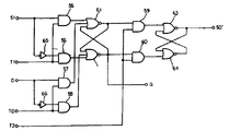
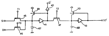
- 적어도 그 중의 1개는 순서회로를 포함한 복수개의 회로 블록간에서 데이터 전송을 실행함과 동시에 상기 각 회로 블록을 스캔테스트방식으로 테스트 가능하게한 반도체 집적회로장치로서 상기 복수개의 회로 블록사이의 각각에 전파되는 데이터의 비트수에 대응하게 설정되며 통상 동작시는 전단회로 블록의 출력 데이터를 그대로 출력하고 테스트 동작시는 전단회로 블록의 출력데이터 또는 스캔테스트용의 테스트 데이터를 외부클럭에 동기하여 유지 출력하고 전체로서 1개의 시프트레지스트 패스로 접속되어서된 복수의 스캔레지스터와 그 데이터 입력단자가 대응하는 스캔레지스터의 데이터 출력단자에 접속설치되며 통상 동작시는 대응하는 스캔레지스터의 출력데이터를 그대로 차단의 회로 블럭에 출력하고 테스트 동작시의 스캔모드에 있어서는 스캔동작전의 대응하는 스캔레지스터의 출력데이터를 유지하여 당해 데이터를 차단의 회로 블록에 계속 인가하고 테스트모드에 있어서는 대응하는 스캔레지스의 출력데이터를 외부 클럭에 동기하여 유지 출력하는 래치회로와 상기 스캔 레지스터의 각각에 장치외부에서 테스트용이 시티얼데이터를 설정하기 위한 테스트데이터 설정수단과 상기 각 스캔레지스터의 데이터를 시티얼데이터로서 장치외부에 순차 출력하기 위한 테스트결과 출력수단과 통상 동작과 테스트 동작의 전환 스캔모드와 테스트모드의 전환을 하는 동작 전환수단과를 구비함을 특징으로 하는 반도체 집적회로장치.
- 제 1 항에 있어서, 상기 스캔레지스터는 제1, 제2의 래치를 보유하고 통상 동작시 및 테스트 동작시의 테스트 모드시에는 상기 제1의 래치만을 통하여 데이터를 출력하고 동작시의 스캔모드시에는 상기 제1 및 제2의 래치를 통하여 테스트 데이터를 출력하는 것을 특징으로 하는 반도체 집적회로장치.
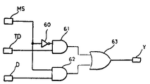
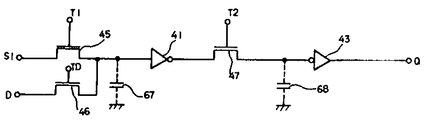
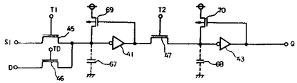
- 제 1 항에 있어서, 스캔인단자(S1)에 접속되어 있는 스캔레지스터(SR)는 제1래치회로 (74)와 제2래치회로 (75)를 테스트동작시의 스캔모드시는 전단회로 블록의 출력데이터를 제1래치회로(74)와 제2래치회로(75)를 거쳐 출력단자(Q)를 통하여 그대로 다음의 스캔레지스터(SR)로 출력하고, 통상 동작시 및 테스트 동작시의 테스트모드시는 출력단자(Q)를 통하여 래치회로도 출력하도록 각 회로 상호간에 시프트레지스터패스로 접속되어서 된 것을 특징으로하는 반도체 집적회로장치.
Applications Claiming Priority (6)
| Application Number | Priority Date | Filing Date | Title |
|---|---|---|---|
| JP183682 | 1986-08-04 | ||
| JP183687 | 1986-08-04 | ||
| JP61183687A JPH0627778B2 (ja) | 1986-08-04 | 1986-08-04 | 半導体集積回路装置 |
| JP61183682A JPH0690261B2 (ja) | 1986-08-04 | 1986-08-04 | 半導体集積回路装置 |
| JP61-183687 | 1986-08-04 | ||
| JP61-183682 | 1986-08-04 |
Publications (2)
| Publication Number | Publication Date |
|---|---|
| KR880003247A KR880003247A (ko) | 1988-05-14 |
| KR900002770B1 true KR900002770B1 (ko) | 1990-04-30 |
Family
ID=26502019
Family Applications (1)
| Application Number | Title | Priority Date | Filing Date |
|---|---|---|---|
| KR1019870004715A KR900002770B1 (ko) | 1986-08-04 | 1987-05-13 | 반도체 집적회로장치 |
Country Status (3)
| Country | Link |
|---|---|
| US (1) | US4864579A (ko) |
| KR (1) | KR900002770B1 (ko) |
| DE (1) | DE3725822A1 (ko) |
Families Citing this family (32)
| Publication number | Priority date | Publication date | Assignee | Title |
|---|---|---|---|---|
| JP2579327B2 (ja) * | 1987-12-04 | 1997-02-05 | 富士通株式会社 | 半導体集積回路 |
| US5189675A (en) * | 1988-06-22 | 1993-02-23 | Kabushiki Kaisha Toshiba | Self-diagnostic circuit for logic circuit block |
| US6304987B1 (en) | 1995-06-07 | 2001-10-16 | Texas Instruments Incorporated | Integrated test circuit |
| NL8900151A (nl) * | 1989-01-23 | 1990-08-16 | Philips Nv | Werkwijze voor het testen van een schakeling, alsmede schakeling geschikt voor een dergelijke werkwijze. |
| JPH0394183A (ja) * | 1989-05-19 | 1991-04-18 | Fujitsu Ltd | 半導体集積回路の試験方法及び回路 |
| JP2632731B2 (ja) * | 1989-08-02 | 1997-07-23 | 三菱電機株式会社 | 集積回路装置 |
| JP2626920B2 (ja) * | 1990-01-23 | 1997-07-02 | 三菱電機株式会社 | スキャンテスト回路およびそれを用いた半導体集積回路装置 |
| JPH0474977A (ja) * | 1990-07-16 | 1992-03-10 | Nec Corp | 半導体集積回路 |
| USRE36292E (en) * | 1990-10-22 | 1999-09-07 | Stmicroelectronics, Inc. | Operational analysis device of the scan path type having a single scanning clock and a single output phase for an integrated circuit |
| IT1246301B (it) * | 1990-10-22 | 1994-11-17 | St Microelectronics Srl | Dispositivo di analisi operativa di tipo scan path a singolo clock di scansione e singola fase di uscita per circuito integrato. |
| US5166604A (en) * | 1990-11-13 | 1992-11-24 | Altera Corporation | Methods and apparatus for facilitating scan testing of asynchronous logic circuitry |
| JP2770617B2 (ja) * | 1991-09-05 | 1998-07-02 | 日本電気株式会社 | テスト回路 |
| US20030133955A1 (en) * | 1993-02-22 | 2003-07-17 | American Bioscience, Inc. | Methods and compositions useful for administration of chemotherapeutic agents |
| JPH06249919A (ja) * | 1993-03-01 | 1994-09-09 | Fujitsu Ltd | 半導体集積回路装置の端子間接続試験方法 |
| US5864565A (en) * | 1993-06-15 | 1999-01-26 | Micron Technology, Inc. | Semiconductor integrated circuit having compression circuitry for compressing test data, and the test system and method for utilizing the semiconductor integrated circuit |
| JP2746076B2 (ja) * | 1993-09-02 | 1998-04-28 | 日本電気株式会社 | 半導体集積回路、その設計方法およびそのテスト方法 |
| JP2768910B2 (ja) * | 1995-02-27 | 1998-06-25 | 日本モトローラ株式会社 | 半導体集積装置におけるスキャンテスト回路 |
| US5656953A (en) * | 1995-05-31 | 1997-08-12 | Texas Instruments Incorporated | Low overhead memory designs for IC terminals |
| US5764079A (en) | 1996-03-11 | 1998-06-09 | Altera Corporation | Sample and load scheme for observability of internal nodes in a PLD |
| JP3039362B2 (ja) * | 1996-03-28 | 2000-05-08 | 日本電気株式会社 | 半導体集積論理回路のテストパターン作成方法 |
| US5867036A (en) * | 1996-05-29 | 1999-02-02 | Lsi Logic Corporation | Domino scan architecture and domino scan flip-flop for the testing of domino and hybrid CMOS circuits |
| US6205566B1 (en) * | 1997-07-23 | 2001-03-20 | Matsushita Electric Industrial Co., Ltd. | Semiconductor integrated circuit, method for designing the same, and storage medium where design program for semiconductor integrated circuit is stored |
| US6202185B1 (en) * | 1997-10-15 | 2001-03-13 | Altera Corporation | Methods and apparatus for facilitating scan testing of circuitry |
| US6157210A (en) | 1997-10-16 | 2000-12-05 | Altera Corporation | Programmable logic device with circuitry for observing programmable logic circuit signals and for preloading programmable logic circuits |
| US6381704B1 (en) * | 1998-01-29 | 2002-04-30 | Texas Instruments Incorporated | Method and apparatus for altering timing relationships of non-overlapping clock signals in a microprocessor |
| US6405335B1 (en) | 1998-02-25 | 2002-06-11 | Texas Instruments Incorporated | Position independent testing of circuits |
| US6728915B2 (en) | 2000-01-10 | 2004-04-27 | Texas Instruments Incorporated | IC with shared scan cells selectively connected in scan path |
| US6769080B2 (en) | 2000-03-09 | 2004-07-27 | Texas Instruments Incorporated | Scan circuit low power adapter with counter |
| JP2004069642A (ja) * | 2002-08-09 | 2004-03-04 | Renesas Technology Corp | 半導体集積回路装置 |
| KR101047533B1 (ko) * | 2007-02-23 | 2011-07-08 | 삼성전자주식회사 | 멀티 페이즈 스캔체인을 구동하는 시스템온칩과 그 방법 |
| US7673206B2 (en) * | 2007-09-14 | 2010-03-02 | Tilera Corporation | Method and system for routing scan chains in an array of processor resources |
| KR102257380B1 (ko) * | 2014-12-22 | 2021-05-31 | 삼성전자주식회사 | 온칩 클록 컨트롤러를 포함하는 시스템온칩 및 이를 포함하는 모바일 장치 |
Family Cites Families (16)
| Publication number | Priority date | Publication date | Assignee | Title |
|---|---|---|---|---|
| US4051352A (en) * | 1976-06-30 | 1977-09-27 | International Business Machines Corporation | Level sensitive embedded array logic system |
| JPS54121036A (en) * | 1978-03-13 | 1979-09-19 | Cho Lsi Gijutsu Kenkyu Kumiai | Method of testing function of logic circuit |
| US4244048A (en) * | 1978-12-29 | 1981-01-06 | International Business Machines Corporation | Chip and wafer configuration and testing method for large-scale-integrated circuits |
| JPS5674668A (en) * | 1979-11-22 | 1981-06-20 | Nec Corp | Logical device |
| DE3029883A1 (de) * | 1980-08-07 | 1982-03-11 | Ibm Deutschland Gmbh, 7000 Stuttgart | Schieberegister fuer pruef- und test-zwecke |
| US4493077A (en) * | 1982-09-09 | 1985-01-08 | At&T Laboratories | Scan testable integrated circuit |
| US4513418A (en) * | 1982-11-08 | 1985-04-23 | International Business Machines Corporation | Simultaneous self-testing system |
| US4580137A (en) * | 1983-08-29 | 1986-04-01 | International Business Machines Corporation | LSSD-testable D-type edge-trigger-operable latch with overriding set/reset asynchronous control |
| US4554664A (en) * | 1983-10-06 | 1985-11-19 | Sperry Corporation | Static memory cell with dynamic scan test latch |
| DE3373729D1 (en) * | 1983-12-08 | 1987-10-22 | Ibm Deutschland | Testing and diagnostic device for a digital calculator |
| AU569401B2 (en) * | 1984-06-22 | 1988-01-28 | Royal Melbourne Institute Of Technology Limited | Slurry viscosity control |
| JPH0772744B2 (ja) * | 1984-09-04 | 1995-08-02 | 株式会社日立製作所 | 半導体集積回路装置 |
| US4703257A (en) * | 1984-12-24 | 1987-10-27 | Hitachi, Ltd. | Logic circuit having a test data scan circuit |
| US4752729A (en) * | 1986-07-01 | 1988-06-21 | Texas Instruments Incorporated | Test circuit for VSLI integrated circuits |
| JPH05228614A (ja) * | 1991-07-04 | 1993-09-07 | Kubota Corp | 遠心鋳鋼管内面のヒケ巣除去法 |
| JPH05274668A (ja) * | 1992-03-25 | 1993-10-22 | Taiyo Yuden Co Ltd | 磁性薄膜の製法 |
-
1987
- 1987-05-13 KR KR1019870004715A patent/KR900002770B1/ko not_active IP Right Cessation
- 1987-08-03 US US07/081,094 patent/US4864579A/en not_active Expired - Lifetime
- 1987-08-04 DE DE3725822A patent/DE3725822A1/de active Granted
Also Published As
| Publication number | Publication date |
|---|---|
| US4864579A (en) | 1989-09-05 |
| KR880003247A (ko) | 1988-05-14 |
| DE3725822A1 (de) | 1988-02-18 |
| DE3725822C2 (ko) | 1990-09-20 |
Similar Documents
| Publication | Publication Date | Title |
|---|---|---|
| KR900002770B1 (ko) | 반도체 집적회로장치 | |
| US5130647A (en) | Scan test circuit and semiconductor integrated circuit device using the same | |
| US4870345A (en) | Semiconductor intergrated circuit device | |
| JP2725258B2 (ja) | 集積回路装置 | |
| US4493077A (en) | Scan testable integrated circuit | |
| US5606567A (en) | Delay testing of high-performance digital components by a slow-speed tester | |
| US5719878A (en) | Scannable storage cell and method of operation | |
| AU593028B2 (en) | Digital intergrated circuit | |
| US6389566B1 (en) | Edge-triggered scan flip-flop and one-pass scan synthesis methodology | |
| US6380780B1 (en) | Integrated circuit with scan flip-flop | |
| KR900002444B1 (ko) | 반도체 집적회로장치 | |
| KR100214239B1 (ko) | 부분 스캔 패스 회로를 갖는 집적 논리 회로와 부분 스캔 패스 설계 방법 | |
| US20040075479A1 (en) | Reducing power and area consumption of gated clock enabled flip flops | |
| KR950024305A (ko) | 논리합성방법 및 반도체집적회로 | |
| US4942577A (en) | Logic circuit system with latch circuits for reliable scan-path testing | |
| JP2946658B2 (ja) | フリップフロップ回路 | |
| US5457698A (en) | Test circuit having a plurality of scan latch circuits | |
| KR910000608B1 (ko) | 반도체 집적회로장치 | |
| JPS6352074A (ja) | 半導体集積回路装置 | |
| KR100292142B1 (ko) | 스캔시험용 플립플롭회로 | |
| van Berkel et al. | Adding synchronous and LSSD modes to asynchronous circuits | |
| US20040019830A1 (en) | Test apparatus of semiconductor integrated circuit with hold error preventing function | |
| US6574169B1 (en) | Delay test system for normal circuit | |
| JPH09243705A (ja) | 半導体論理集積回路 | |
| KR960030412A (ko) | 스캔 경로를 가지는 반도체 장치 |
Legal Events
| Date | Code | Title | Description |
|---|---|---|---|
| A201 | Request for examination | ||
| PA0109 | Patent application |
Patent event code: PA01091R01D Comment text: Patent Application Patent event date: 19870513 |
|
| PA0201 | Request for examination |
Patent event code: PA02012R01D Patent event date: 19870513 Comment text: Request for Examination of Application |
|
| PG1501 | Laying open of application | ||
| G160 | Decision to publish patent application | ||
| PG1605 | Publication of application before grant of patent |
Comment text: Decision on Publication of Application Patent event code: PG16051S01I Patent event date: 19900331 |
|
| E701 | Decision to grant or registration of patent right | ||
| PE0701 | Decision of registration |
Patent event code: PE07011S01D Comment text: Decision to Grant Registration Patent event date: 19900719 |
|
| GRNT | Written decision to grant | ||
| PR0701 | Registration of establishment |
Comment text: Registration of Establishment Patent event date: 19900727 Patent event code: PR07011E01D |
|
| PR1002 | Payment of registration fee |
Payment date: 19900727 End annual number: 3 Start annual number: 1 |
|
| PR1001 | Payment of annual fee |
Payment date: 19930319 Start annual number: 4 End annual number: 4 |
|
| PR1001 | Payment of annual fee |
Payment date: 19940402 Start annual number: 5 End annual number: 5 |
|
| PR1001 | Payment of annual fee |
Payment date: 19950403 Start annual number: 6 End annual number: 6 |
|
| PR1001 | Payment of annual fee |
Payment date: 19960419 Start annual number: 7 End annual number: 7 |
|
| PR1001 | Payment of annual fee |
Payment date: 19970422 Start annual number: 8 End annual number: 8 |
|
| PR1001 | Payment of annual fee |
Payment date: 19980421 Start annual number: 9 End annual number: 9 |
|
| PR1001 | Payment of annual fee |
Payment date: 19990413 Start annual number: 10 End annual number: 10 |
|
| PR1001 | Payment of annual fee |
Payment date: 20000419 Start annual number: 11 End annual number: 11 |
|
| PR1001 | Payment of annual fee |
Payment date: 20010425 Start annual number: 12 End annual number: 12 |
|
| PR1001 | Payment of annual fee |
Payment date: 20020424 Start annual number: 13 End annual number: 13 |
|
| PR1001 | Payment of annual fee |
Payment date: 20030424 Start annual number: 14 End annual number: 14 |
|
| PR1001 | Payment of annual fee |
Payment date: 20040323 Start annual number: 15 End annual number: 15 |
|
| PR1001 | Payment of annual fee |
Payment date: 20050422 Start annual number: 16 End annual number: 16 |
|
| PR1001 | Payment of annual fee |
Payment date: 20060420 Start annual number: 17 End annual number: 17 |
|
| FPAY | Annual fee payment |
Payment date: 20070424 Year of fee payment: 18 |
|
| PR1001 | Payment of annual fee |
Payment date: 20070424 Start annual number: 18 End annual number: 18 |
|
| EXPY | Expiration of term | ||
| PC1801 | Expiration of term |