KR20180098421A - 팩토리 인터페이스 환경 제어들을 갖는 기판 프로세싱 시스템들, 장치, 및 방법들 - Google Patents
팩토리 인터페이스 환경 제어들을 갖는 기판 프로세싱 시스템들, 장치, 및 방법들 Download PDFInfo
- Publication number
- KR20180098421A KR20180098421A KR1020187024379A KR20187024379A KR20180098421A KR 20180098421 A KR20180098421 A KR 20180098421A KR 1020187024379 A KR1020187024379 A KR 1020187024379A KR 20187024379 A KR20187024379 A KR 20187024379A KR 20180098421 A KR20180098421 A KR 20180098421A
- Authority
- KR
- South Korea
- Prior art keywords
- factory interface
- electronic device
- processing system
- chamber
- device processing
- Prior art date
- Legal status (The legal status is an assumption and is not a legal conclusion. Google has not performed a legal analysis and makes no representation as to the accuracy of the status listed.)
- Granted
Links
Images


Classifications
-
- H01L21/67253—
-
- H—ELECTRICITY
- H10—SEMICONDUCTOR DEVICES; ELECTRIC SOLID-STATE DEVICES NOT OTHERWISE PROVIDED FOR
- H10P—GENERIC PROCESSES OR APPARATUS FOR THE MANUFACTURE OR TREATMENT OF DEVICES COVERED BY CLASS H10
- H10P72/00—Handling or holding of wafers, substrates or devices during manufacture or treatment thereof
- H10P72/04—Apparatus for manufacture or treatment
- H10P72/0451—Apparatus for manufacturing or treating in a plurality of work-stations
- H10P72/0468—Apparatus for manufacturing or treating in a plurality of work-stations comprising a chamber adapted to a particular process
-
- H01L21/67028—
-
- H01L21/67207—
-
- H01L21/67248—
-
- H01L21/67772—
-
- H01L22/30—
-
- H—ELECTRICITY
- H10—SEMICONDUCTOR DEVICES; ELECTRIC SOLID-STATE DEVICES NOT OTHERWISE PROVIDED FOR
- H10P—GENERIC PROCESSES OR APPARATUS FOR THE MANUFACTURE OR TREATMENT OF DEVICES COVERED BY CLASS H10
- H10P72/00—Handling or holding of wafers, substrates or devices during manufacture or treatment thereof
- H10P72/04—Apparatus for manufacture or treatment
- H10P72/0402—Apparatus for fluid treatment
- H10P72/0406—Apparatus for fluid treatment for cleaning followed by drying, rinsing, stripping, blasting or the like
-
- H—ELECTRICITY
- H10—SEMICONDUCTOR DEVICES; ELECTRIC SOLID-STATE DEVICES NOT OTHERWISE PROVIDED FOR
- H10P—GENERIC PROCESSES OR APPARATUS FOR THE MANUFACTURE OR TREATMENT OF DEVICES COVERED BY CLASS H10
- H10P72/00—Handling or holding of wafers, substrates or devices during manufacture or treatment thereof
- H10P72/06—Apparatus for monitoring, sorting, marking, testing or measuring
- H10P72/0602—Temperature monitoring
-
- H—ELECTRICITY
- H10—SEMICONDUCTOR DEVICES; ELECTRIC SOLID-STATE DEVICES NOT OTHERWISE PROVIDED FOR
- H10P—GENERIC PROCESSES OR APPARATUS FOR THE MANUFACTURE OR TREATMENT OF DEVICES COVERED BY CLASS H10
- H10P72/00—Handling or holding of wafers, substrates or devices during manufacture or treatment thereof
- H10P72/06—Apparatus for monitoring, sorting, marking, testing or measuring
- H10P72/0604—Process monitoring, e.g. flow or thickness monitoring
-
- H—ELECTRICITY
- H10—SEMICONDUCTOR DEVICES; ELECTRIC SOLID-STATE DEVICES NOT OTHERWISE PROVIDED FOR
- H10P—GENERIC PROCESSES OR APPARATUS FOR THE MANUFACTURE OR TREATMENT OF DEVICES COVERED BY CLASS H10
- H10P74/00—Testing or measuring during manufacture or treatment of wafers, substrates or devices
- H10P74/27—Structural arrangements therefor
-
- H—ELECTRICITY
- H10—SEMICONDUCTOR DEVICES; ELECTRIC SOLID-STATE DEVICES NOT OTHERWISE PROVIDED FOR
- H10P—GENERIC PROCESSES OR APPARATUS FOR THE MANUFACTURE OR TREATMENT OF DEVICES COVERED BY CLASS H10
- H10P72/00—Handling or holding of wafers, substrates or devices during manufacture or treatment thereof
- H10P72/30—Handling or holding of wafers, substrates or devices during manufacture or treatment thereof for conveying, e.g. between different workstations
- H10P72/34—Handling or holding of wafers, substrates or devices during manufacture or treatment thereof for conveying, e.g. between different workstations the wafers being stored in a carrier, involving loading and unloading
- H10P72/3406—Handling or holding of wafers, substrates or devices during manufacture or treatment thereof for conveying, e.g. between different workstations the wafers being stored in a carrier, involving loading and unloading involving removal of lid, door or cover
Landscapes
- Container, Conveyance, Adherence, Positioning, Of Wafer (AREA)
- Engineering & Computer Science (AREA)
- Manufacturing & Machinery (AREA)
- Exposure Of Semiconductors, Excluding Electron Or Ion Beam Exposure (AREA)
- Cleaning Or Drying Semiconductors (AREA)
- Drying Of Semiconductors (AREA)
- Physics & Mathematics (AREA)
- General Physics & Mathematics (AREA)
- Automation & Control Theory (AREA)
Abstract
Description
[00011] 도 1은, 실시예들에 따른, 팩토리 인터페이스 환경 제어들을 포함하는 전자 디바이스 프로세싱 시스템의 개략적인 상면도를 예시한다.
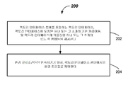
[00012] 도 2는, 실시예들에 따른, 전자 디바이스 프로세싱 시스템 내에서 기판들을 프로세싱하는 방법을 도시하는 흐름도를 예시한다.
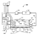
[00013] 도 3은, 실시예들에 따른, 비활성 가스 재순환(recirculation) 시스템을 포함하는 전자 디바이스 프로세싱 시스템의 개략적인 상면도를 예시한다.
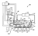
[00014] 도 4는, 실시예들에 따른, 환경 제어들 및 비활성 가스 재순환을 포함하는 다른 전자 디바이스 프로세싱 시스템의 개략적인 상면도를 예시한다.
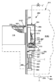
[00015] 도 5a는, 실시예들에 따른 캐리어 퍼지 어셈블리의 측단면도를 예시한다.
[00016] 도 5b는, 실시예들에 따른 캐리어 퍼지 어셈블리의 정면도를 예시한다.
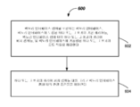
[00017] 도 6은, 실시예들에 따른, 전자 디바이스 프로세싱 시스템 내에서 기판들을 프로세싱하는 방법을 도시하는 다른 흐름도를 예시한다.
Claims (20)
- 전자 디바이스 프로세싱 시스템으로서,
팩토리 인터페이스 챔버를 포함하는 팩토리 인터페이스;
상기 팩토리 인터페이스에 커플링된 로드 락 장치;
상기 팩토리 인터페이스에 커플링된 하나 또는 그 초과의 기판 캐리어들; 및
상기 팩토리 인터페이스에 커플링된 환경 제어 시스템
을 포함하며,
상기 환경 제어 시스템은:
상기 팩토리 인터페이스 챔버 내로의 비활성 가스의 양을 제어하고; 그리고
상기 팩토리 인터페이스 챔버로부터 배기되는 상기 비활성 가스를 다시 상기 팩토리 인터페이스 챔버 내로 재순환시키도록 동작하는,
전자 디바이스 프로세싱 시스템. - 제 1 항에 있어서,
배기 도관을 더 포함하고, 상기 비활성 가스는 상기 배기 도관을 거쳐 적어도 부분적으로 재순환되는,
전자 디바이스 프로세싱 시스템. - 제 2 항에 있어서,
상기 배기 도관에 직렬로 연결된 필터를 더 포함하는,
전자 디바이스 프로세싱 시스템. - 제 3 항에 있어서,
상기 필터는 미립자들을 필터링하도록 구성되는,
전자 디바이스 프로세싱 시스템. - 제 3 항에 있어서,
상기 필터는 습기-감소(moisture-reducing) 필터인,
전자 디바이스 프로세싱 시스템. - 제 3 항에 있어서,
상기 필터는 습기-흡수성(moisture-absorbent) 필터인,
전자 디바이스 프로세싱 시스템. - 제 3 항에 있어서,
상기 필터는 상기 팩토리 인터페이스 챔버 내에 있는,
전자 디바이스 프로세싱 시스템. - 제 2 항에 있어서,
상기 팩토리 인터페이스 챔버 상의 챔버 도어; 및
상기 챔버 도어 내의 채널
을 더 포함하고, 상기 채널은 상기 팩토리 인터페이스 챔버로부터의 입구를 가지며, 상기 채널은 상기 배기 도관에 커플링되는,
전자 디바이스 프로세싱 시스템. - 제 8 항에 있어서,
상기 챔버 도어는 바닥을 가지며, 상기 채널의 입구는 상기 챔버 도어의 상기 바닥에 인접한,
전자 디바이스 프로세싱 시스템. - 제 9 항에 있어서,
상기 배기 도관 내에 직렬로 연결된 필터를 더 포함하고, 상기 챔버 도어와 상기 필터 사이의 상기 배기 도관은 상기 필터 위에서 진행하는,
전자 디바이스 프로세싱 시스템. - 전자 디바이스 프로세싱 시스템으로서,
팩토리 인터페이스 챔버를 포함하는 팩토리 인터페이스;
상기 팩토리 인터페이스에 커플링된 로드 락 장치;
상기 팩토리 인터페이스에 커플링된 하나 또는 그 초과의 기판 캐리어들;
상기 팩토리 인터페이스 챔버에 커플링되는 비활성 가스 공급부;
상기 팩토리 인터페이스 챔버 내로의 비활성 가스 유동 및 상기 팩토리 인터페이스 챔버 내의 가스 압력 중 적어도 하나를 나타내는 하나 또는 그 초과의 신호들을 생성하도록 동작하는 하나 또는 그 초과의 센서들; 및
상기 하나 또는 그 초과의 센서들에 커플링되는 제어기를 더 포함하고,
상기 제어기는:
상기 하나 또는 그 초과의 신호들을 모니터링하고; 그리고
상기 하나 또는 그 초과의 신호들이 미리-설정된 제한 밖에 있는 경우에 응답하여 신호를 생성하는 것에 의해
누설을 결정하도록 동작하는,
전자 디바이스 프로세싱 시스템. - 제 11 항에 있어서,
상기 비활성 가스 공급부와 상기 팩토리 인터페이스 챔버 사이에 커플링되는 전달 라인을 더 포함하고, 상기 하나 또는 그 초과의 센서들은 상기 전달 라인 내의 유동 센서인,
전자 디바이스 프로세싱 시스템. - 제 12 항에 있어서,
상기 유동 센서는 상기 전달 라인을 통해 비활성 가스를 나타내는 하나 또는 그 초과의 신호들을 생성하고, 신호를 생성하는 것은 상기 비활성 가스 유동이 미리-설정된 제한 밖에 있는 경우에 응답하여 신호를 생성하는 것을 포함하는,
전자 디바이스 프로세싱 시스템. - 제 11 항에 있어서,
상기 하나 또는 그 초과의 센서들은 상기 팩토리 인터페이스 챔버 내에 위치된 압력 센서를 포함하는,
전자 디바이스 프로세싱 시스템. - 제 14 항에 있어서,
상기 압력 센서는 상기 팩토리 인터페이스 챔버 내의 압력을 나타내는 하나 또는 그 초과의 신호들을 생성하고, 신호를 생성하는 것은 상기 압력이 미리-설정된 제한 밖에 있는 경우에 응답하여 신호를 생성하는 것을 포함하는,
전자 디바이스 프로세싱 시스템. - 제 15 항에 있어서,
신호를 생성하는 것은 상기 압력이 미리-설정된 제한 아래에 있는 경우에 응답하여 신호를 생성하는 것을 포함하는,
전자 디바이스 프로세싱 시스템. - 제 16 항에 있어서,
상기 미리-설정된 제한은 500 Pa인,
전자 디바이스 프로세싱 시스템. - 제 11 항에 있어서,
상기 비활성 가스 공급부 및 상기 팩토리 인터페이스 챔버 사이에 커플링되는 전달 라인을 더 포함하고, 상기 하나 또는 그 초과의 센서들은 상기 전달 라인 내의 유동 센서이고, 하나 또는 그 초과의 센서들은 상기 팩토리 인터페이스 챔버 내의 압력 센서인,
전자 디바이스 프로세싱 시스템. - 제 18 항에 있어서,
신호를 생성하는 것은 상기 압력이 미리-설정된 제한 아래에 있거나 또는 상기 비활성 가스 유동이 미리-설정된 제한 밖에 있는 경우에 응답하여 신호를 생성하는 것을 포함하는,
전자 디바이스 프로세싱 시스템. - 제 18 항에 있어서,
상기 비활성 가스는 아르곤(Ar), 질소(N2) 가스, 또는 헬륨(He)을 포함하는,
전자 디바이스 프로세싱 시스템.
Priority Applications (1)
| Application Number | Priority Date | Filing Date | Title |
|---|---|---|---|
| KR1020197024815A KR102297447B1 (ko) | 2013-08-12 | 2014-08-11 | 팩토리 인터페이스 환경 제어들을 갖는 기판 프로세싱 시스템들, 장치, 및 방법들 |
Applications Claiming Priority (3)
| Application Number | Priority Date | Filing Date | Title |
|---|---|---|---|
| US201361865046P | 2013-08-12 | 2013-08-12 | |
| US61/865,046 | 2013-08-12 | ||
| PCT/US2014/050561 WO2015023591A1 (en) | 2013-08-12 | 2014-08-11 | Substrate processing systems, apparatus, and methods with factory interface environmental controls |
Related Parent Applications (1)
| Application Number | Title | Priority Date | Filing Date |
|---|---|---|---|
| KR1020167006455A Division KR20160043027A (ko) | 2013-08-12 | 2014-08-11 | 팩토리 인터페이스 환경 제어들을 갖는 기판 프로세싱 시스템들, 장치, 및 방법들 |
Related Child Applications (1)
| Application Number | Title | Priority Date | Filing Date |
|---|---|---|---|
| KR1020197024815A Division KR102297447B1 (ko) | 2013-08-12 | 2014-08-11 | 팩토리 인터페이스 환경 제어들을 갖는 기판 프로세싱 시스템들, 장치, 및 방법들 |
Publications (2)
| Publication Number | Publication Date |
|---|---|
| KR20180098421A true KR20180098421A (ko) | 2018-09-03 |
| KR102234464B1 KR102234464B1 (ko) | 2021-03-30 |
Family
ID=52449296
Family Applications (6)
| Application Number | Title | Priority Date | Filing Date |
|---|---|---|---|
| KR1020197024815A Active KR102297447B1 (ko) | 2013-08-12 | 2014-08-11 | 팩토리 인터페이스 환경 제어들을 갖는 기판 프로세싱 시스템들, 장치, 및 방법들 |
| KR1020167006455A Ceased KR20160043027A (ko) | 2013-08-12 | 2014-08-11 | 팩토리 인터페이스 환경 제어들을 갖는 기판 프로세싱 시스템들, 장치, 및 방법들 |
| KR1020227028568A Ceased KR20220120714A (ko) | 2013-08-12 | 2014-08-11 | 팩토리 인터페이스 환경 제어들을 갖는 기판 프로세싱 시스템들, 장치, 및 방법들 |
| KR1020247033706A Pending KR20240152961A (ko) | 2013-08-12 | 2014-08-11 | 팩토리 인터페이스 환경 제어들을 갖는 기판 프로세싱 시스템들, 장치, 및 방법들 |
| KR1020187024379A Active KR102234464B1 (ko) | 2013-08-12 | 2014-08-11 | 팩토리 인터페이스 환경 제어들을 갖는 기판 프로세싱 시스템들, 장치, 및 방법들 |
| KR1020217027565A Active KR102435429B1 (ko) | 2013-08-12 | 2014-08-11 | 팩토리 인터페이스 환경 제어들을 갖는 기판 프로세싱 시스템들, 장치, 및 방법들 |
Family Applications Before (4)
| Application Number | Title | Priority Date | Filing Date |
|---|---|---|---|
| KR1020197024815A Active KR102297447B1 (ko) | 2013-08-12 | 2014-08-11 | 팩토리 인터페이스 환경 제어들을 갖는 기판 프로세싱 시스템들, 장치, 및 방법들 |
| KR1020167006455A Ceased KR20160043027A (ko) | 2013-08-12 | 2014-08-11 | 팩토리 인터페이스 환경 제어들을 갖는 기판 프로세싱 시스템들, 장치, 및 방법들 |
| KR1020227028568A Ceased KR20220120714A (ko) | 2013-08-12 | 2014-08-11 | 팩토리 인터페이스 환경 제어들을 갖는 기판 프로세싱 시스템들, 장치, 및 방법들 |
| KR1020247033706A Pending KR20240152961A (ko) | 2013-08-12 | 2014-08-11 | 팩토리 인터페이스 환경 제어들을 갖는 기판 프로세싱 시스템들, 장치, 및 방법들 |
Family Applications After (1)
| Application Number | Title | Priority Date | Filing Date |
|---|---|---|---|
| KR1020217027565A Active KR102435429B1 (ko) | 2013-08-12 | 2014-08-11 | 팩토리 인터페이스 환경 제어들을 갖는 기판 프로세싱 시스템들, 장치, 및 방법들 |
Country Status (6)
| Country | Link |
|---|---|
| US (4) | US10192765B2 (ko) |
| JP (6) | JP6526660B6 (ko) |
| KR (6) | KR102297447B1 (ko) |
| CN (6) | CN105453246A (ko) |
| TW (6) | TWI902104B (ko) |
| WO (1) | WO2015023591A1 (ko) |
Families Citing this family (57)
| Publication number | Priority date | Publication date | Assignee | Title |
|---|---|---|---|---|
| CN105453246A (zh) | 2013-08-12 | 2016-03-30 | 应用材料公司 | 具有工厂接口环境控制的基板处理系统、装置和方法 |
| US9698041B2 (en) | 2014-06-09 | 2017-07-04 | Applied Materials, Inc. | Substrate temperature control apparatus including optical fiber heating, substrate temperature control systems, electronic device processing systems, and methods |
| JP6608923B2 (ja) * | 2014-07-02 | 2019-11-20 | アプライド マテリアルズ インコーポレイテッド | 溝に経路指定された光ファイバーによる加熱を含む温度制御装置、基板温度制御システム、電子デバイス処理システム、及び処理方法 |
| JP6822953B2 (ja) * | 2014-11-25 | 2021-01-27 | アプライド マテリアルズ インコーポレイテッドApplied Materials,Incorporated | 基板キャリア及びパージチャンバの環境制御を伴う基板処理のシステム、装置、及び方法 |
| JP6458595B2 (ja) * | 2015-03-27 | 2019-01-30 | 東京エレクトロン株式会社 | 成膜装置及び成膜方法並びに記憶媒体 |
| WO2016190982A1 (en) | 2015-05-22 | 2016-12-01 | Applied Materials, Inc | Substrate carrier door assemblies, substrate carriers, and methods including magnetic door seal |
| TWI727562B (zh) * | 2015-08-04 | 2021-05-11 | 日商昕芙旎雅股份有限公司 | 裝載埠 |
| TWI878060B (zh) | 2015-08-04 | 2025-03-21 | 日商昕芙旎雅股份有限公司 | 門開閉系統及具備門開閉系統之載入埠 |
| TWI780030B (zh) * | 2015-10-05 | 2022-10-11 | 德商布魯克斯Ccs有限公司 | 形成用於一半導體基板並具有低溼度值的一乾淨的環境的方法及系統 |
| US10520371B2 (en) | 2015-10-22 | 2019-12-31 | Applied Materials, Inc. | Optical fiber temperature sensors, temperature monitoring apparatus, and manufacturing methods |
| US10119191B2 (en) | 2016-06-08 | 2018-11-06 | Applied Materials, Inc. | High flow gas diffuser assemblies, systems, and methods |
| US10684159B2 (en) | 2016-06-27 | 2020-06-16 | Applied Materials, Inc. | Methods, systems, and apparatus for mass flow verification based on choked flow |
| JP6903883B2 (ja) * | 2016-09-09 | 2021-07-14 | Tdk株式会社 | 容器内清浄化装置 |
| JP6842156B2 (ja) * | 2016-10-25 | 2021-03-17 | 株式会社システック | 防爆恒温槽 |
| US10159169B2 (en) | 2016-10-27 | 2018-12-18 | Applied Materials, Inc. | Flexible equipment front end module interfaces, environmentally-controlled equipment front end modules, and assembly methods |
| US10453727B2 (en) | 2016-11-10 | 2019-10-22 | Applied Materials, Inc. | Electronic device manufacturing load port apparatus, systems, and methods |
| US10262884B2 (en) * | 2016-11-10 | 2019-04-16 | Applied Materials, Inc. | Systems, apparatus, and methods for an improved load port |
| US10541165B2 (en) | 2016-11-10 | 2020-01-21 | Applied Materials, Inc. | Systems, apparatus, and methods for an improved load port backplane |
| US10453726B2 (en) | 2016-11-10 | 2019-10-22 | Applied Materials, Inc. | Electronic device manufacturing load port apparatus, systems, and methods |
| US10741432B2 (en) * | 2017-02-06 | 2020-08-11 | Applied Materials, Inc. | Systems, apparatus, and methods for a load port door opener |
| JP7158133B2 (ja) * | 2017-03-03 | 2022-10-21 | アプライド マテリアルズ インコーポレイテッド | 雰囲気が制御された移送モジュール及び処理システム |
| US10446428B2 (en) | 2017-03-14 | 2019-10-15 | Applied Materials, Inc. | Load port operation in electronic device manufacturing apparatus, systems, and methods |
| US10796935B2 (en) * | 2017-03-17 | 2020-10-06 | Applied Materials, Inc. | Electronic device manufacturing systems, methods, and apparatus for heating substrates and reducing contamination in loadlocks |
| US11133208B2 (en) * | 2017-05-31 | 2021-09-28 | Tdk Corporation | EFEM and method of introducing dry air thereinto |
| US10388547B2 (en) * | 2017-06-23 | 2019-08-20 | Applied Materials, Inc. | Side storage pods, equipment front end modules, and methods for processing substrates |
| TWI717034B (zh) | 2017-06-23 | 2021-01-21 | 美商應用材料股份有限公司 | 側儲存倉、電子裝置處理系統、和處理基板的方法 |
| US10361099B2 (en) * | 2017-06-23 | 2019-07-23 | Applied Materials, Inc. | Systems and methods of gap calibration via direct component contact in electronic device manufacturing systems |
| US10763134B2 (en) * | 2018-02-27 | 2020-09-01 | Applied Materials, Inc. | Substrate processing apparatus and methods with factory interface chamber filter purge |
| JP7125589B2 (ja) * | 2018-03-15 | 2022-08-25 | シンフォニアテクノロジー株式会社 | Efemシステム及びefemシステムにおけるガス供給方法 |
| US10403514B1 (en) * | 2018-04-12 | 2019-09-03 | Asm Ip Holding B.V. | Substrate transporting system, storage medium and substrate transporting method |
| US20190362989A1 (en) * | 2018-05-25 | 2019-11-28 | Applied Materials, Inc. | Substrate manufacturing apparatus and methods with factory interface chamber heating |
| JP6876020B2 (ja) * | 2018-07-27 | 2021-05-26 | 株式会社Kokusai Electric | 基板処理装置および半導体装置の製造方法並びにプログラム |
| US10529602B1 (en) * | 2018-11-13 | 2020-01-07 | Applied Materials, Inc. | Method and apparatus for substrate fabrication |
| US11189511B2 (en) * | 2018-10-26 | 2021-11-30 | Applied Materials, Inc. | Side storage pods, equipment front end modules, and methods for operating EFEMs |
| US11373891B2 (en) * | 2018-10-26 | 2022-06-28 | Applied Materials, Inc. | Front-ducted equipment front end modules, side storage pods, and methods of operating the same |
| US11244844B2 (en) * | 2018-10-26 | 2022-02-08 | Applied Materials, Inc. | High flow velocity, gas-purged, side storage pod apparatus, assemblies, and methods |
| KR102728796B1 (ko) * | 2019-03-20 | 2024-11-12 | 삼성전자주식회사 | 반도체 기판의 열처리 장치 |
| JP7221110B2 (ja) * | 2019-03-28 | 2023-02-13 | 株式会社Screenホールディングス | 基板処理装置 |
| TWI737996B (zh) * | 2019-05-16 | 2021-09-01 | 華景電通股份有限公司 | 晶圓載具監控系統及其監控方法 |
| JP7379042B2 (ja) * | 2019-09-20 | 2023-11-14 | 東京エレクトロン株式会社 | 真空搬送装置および真空搬送装置の制御方法 |
| CN111090295A (zh) * | 2019-12-31 | 2020-05-01 | 北京海岚科技有限公司 | Efem中环境参数的控制方法及控制系统 |
| CN113113326B (zh) * | 2020-01-10 | 2024-12-27 | 台湾积体电路制造股份有限公司 | 半导体制程机台 |
| US20210407837A1 (en) * | 2020-06-30 | 2021-12-30 | Applied Materials, Inc. | Robot apparatus and systems, and methods for transporting substrates in electronic device manufacturing |
| US11810805B2 (en) * | 2020-07-09 | 2023-11-07 | Applied Materials, Inc. | Prevention of contamination of substrates during gas purging |
| US11996307B2 (en) * | 2020-12-23 | 2024-05-28 | Applied Materials, Inc. | Semiconductor processing tool platform configuration with reduced footprint |
| JP7154325B2 (ja) * | 2021-01-20 | 2022-10-17 | 株式会社Kokusai Electric | 基板処理装置、半導体装置の製造方法およびプログラム |
| US12159802B2 (en) * | 2021-03-04 | 2024-12-03 | Applied Materials, Inc. | Shortened load port for factory interface |
| US11854851B2 (en) * | 2021-03-05 | 2023-12-26 | Taiwan Semiconductor Manufacturing Company, Ltd. | Interface tool |
| WO2022201831A1 (ja) * | 2021-03-25 | 2022-09-29 | 株式会社Screenホールディングス | 処理液キャビネットの排気制御方法および基板処理装置 |
| KR102592612B1 (ko) | 2021-08-24 | 2023-10-24 | (주)옵토레인 | 분자 진단 카트리지 |
| JP7698198B2 (ja) * | 2021-08-26 | 2025-06-25 | シンフォニアテクノロジー株式会社 | Efem、不活性ガス供給制御方法 |
| JP7430677B2 (ja) * | 2021-09-21 | 2024-02-13 | 株式会社Kokusai Electric | 基板処理装置、半導体装置の製造方法およびプログラム |
| US11756925B2 (en) * | 2021-10-22 | 2023-09-12 | Applied Materials, Inc. | Methods and apparatus for vacuum processing a substrate |
| KR20250086703A (ko) * | 2022-10-10 | 2025-06-13 | 램 리써치 코포레이션 | 기판 프로세싱 챔버들로부터의 독성 및 부식성 재료 퍼지 |
| KR20250073237A (ko) * | 2022-11-07 | 2025-05-27 | 주식회사 히타치하이테크 | 웨이퍼 반송 장치 |
| US20240153787A1 (en) * | 2022-11-07 | 2024-05-09 | Taiwan Semiconductor Manufacturing Co., Ltd. | Control of environment within processing modules |
| KR102925708B1 (ko) * | 2023-12-18 | 2026-02-10 | (주)아이디온 | 반도체 공정을 위한 웨이퍼 캐리어 실시간 모니터링 시스템 및 방법 |
Citations (4)
| Publication number | Priority date | Publication date | Assignee | Title |
|---|---|---|---|---|
| JPH07138092A (ja) * | 1993-11-15 | 1995-05-30 | Nec Corp | 分子線結晶成長装置 |
| KR100505061B1 (ko) * | 2003-02-12 | 2005-08-01 | 삼성전자주식회사 | 기판 이송 모듈 |
| JP2009117554A (ja) * | 2007-11-05 | 2009-05-28 | Hitachi Kokusai Electric Inc | 基板処理装置 |
| WO2012133441A1 (ja) * | 2011-03-28 | 2012-10-04 | 株式会社日立国際電気 | 基板処理装置、半導体装置の製造方法及び基板処理方法 |
Family Cites Families (116)
| Publication number | Priority date | Publication date | Assignee | Title |
|---|---|---|---|---|
| US3688540A (en) * | 1969-07-29 | 1972-09-05 | Superior Tube Co | Tube rolling mill employing a tapered mandrel and a cluster of rolls that each have specially designed tube contacting grooves |
| JPS62222625A (ja) * | 1986-03-25 | 1987-09-30 | Shimizu Constr Co Ltd | 半導体製造装置 |
| US5186594A (en) | 1990-04-19 | 1993-02-16 | Applied Materials, Inc. | Dual cassette load lock |
| JPH05326421A (ja) * | 1992-05-20 | 1993-12-10 | Fujitsu Ltd | 成膜方法 |
| JPH0634479A (ja) | 1992-07-16 | 1994-02-08 | Toshiba Ceramics Co Ltd | 半導体用熱処理炉のガスリーク検知方法および装置 |
| US5527390A (en) * | 1993-03-19 | 1996-06-18 | Tokyo Electron Kabushiki | Treatment system including a plurality of treatment apparatus |
| KR100221983B1 (ko) * | 1993-04-13 | 1999-09-15 | 히가시 데쓰로 | 처리장치 |
| JPH07226382A (ja) * | 1994-02-10 | 1995-08-22 | Tokyo Electron Ltd | 熱処理装置 |
| JP2885142B2 (ja) * | 1995-08-16 | 1999-04-19 | 日本電気株式会社 | 真空処理装置及び真空処理装置への大気混入の検知方法 |
| JP2806919B2 (ja) | 1996-12-25 | 1998-09-30 | 日本電気ファクトリエンジニアリング株式会社 | 恒温槽 |
| JPH10270535A (ja) | 1997-03-25 | 1998-10-09 | Nikon Corp | 移動ステージ装置、及び該ステージ装置を用いた回路デバイス製造方法 |
| JP3839555B2 (ja) * | 1997-06-05 | 2006-11-01 | 高砂熱学工業株式会社 | 局所密閉型清浄装置 |
| JP3425592B2 (ja) * | 1997-08-12 | 2003-07-14 | 東京エレクトロン株式会社 | 処理装置 |
| JPH11312640A (ja) | 1998-02-25 | 1999-11-09 | Canon Inc | 処理装置および該処理装置を用いたデバイス製造方法 |
| JP2000058619A (ja) * | 1998-08-07 | 2000-02-25 | Kokusai Electric Co Ltd | 基板処理装置及び基板処理方法 |
| JP2000150613A (ja) * | 1998-11-17 | 2000-05-30 | Tokyo Electron Ltd | 被処理体の搬送装置 |
| JP2000296309A (ja) | 1999-04-12 | 2000-10-24 | Daikin Ind Ltd | 半導体製造システム |
| US6877219B1 (en) * | 1999-10-26 | 2005-04-12 | Air Liquide America, L.P. | Apparatus for placing components on printed circuit boards |
| JP2001284433A (ja) | 2000-01-28 | 2001-10-12 | Sony Corp | 基板移載装置及び基板移載方法 |
| US7147424B2 (en) | 2000-07-07 | 2006-12-12 | Applied Materials, Inc. | Automatic door opener |
| KR100745867B1 (ko) * | 2000-08-23 | 2007-08-02 | 동경 엘렉트론 주식회사 | 수직열처리장치 및 피처리체를 운송하는 방법 |
| US6690993B2 (en) | 2000-10-12 | 2004-02-10 | R. Foulke Development Company, Llc | Reticle storage system |
| JP3939101B2 (ja) * | 2000-12-04 | 2007-07-04 | 株式会社荏原製作所 | 基板搬送方法および基板搬送容器 |
| JP2002350925A (ja) * | 2001-05-30 | 2002-12-04 | Fuji Photo Film Co Ltd | カメラの絞り切換え装置 |
| US6585470B2 (en) | 2001-06-19 | 2003-07-01 | Brooks Automation, Inc. | System for transporting substrates |
| US20030031538A1 (en) | 2001-06-30 | 2003-02-13 | Applied Materials, Inc. | Datum plate for use in installations of substrate handling systems |
| US8796589B2 (en) | 2001-07-15 | 2014-08-05 | Applied Materials, Inc. | Processing system with the dual end-effector handling |
| US6819517B2 (en) * | 2001-07-31 | 2004-11-16 | Seagate Technology Llc | Disc drive servo track writer gas leak detector and method |
| JP3880343B2 (ja) * | 2001-08-01 | 2007-02-14 | 株式会社ルネサステクノロジ | ロードポート、基板処理装置および雰囲気置換方法 |
| US6672864B2 (en) * | 2001-08-31 | 2004-01-06 | Applied Materials, Inc. | Method and apparatus for processing substrates in a system having high and low pressure areas |
| JP3950698B2 (ja) | 2002-02-08 | 2007-08-01 | キヤノン株式会社 | 半導体露光装置 |
| US6828234B2 (en) * | 2002-03-26 | 2004-12-07 | Applied Materials, Inc. | RTP process chamber pressure control |
| JP4218821B2 (ja) | 2002-06-11 | 2009-02-04 | 株式会社日立国際電気 | 基板処理装置 |
| US6846380B2 (en) * | 2002-06-13 | 2005-01-25 | The Boc Group, Inc. | Substrate processing apparatus and related systems and methods |
| TW554421B (en) * | 2002-08-22 | 2003-09-21 | Promos Technologies Inc | A front open unified pod door opener with a dust-proof means |
| US7258520B2 (en) | 2002-08-31 | 2007-08-21 | Applied Materials, Inc. | Methods and apparatus for using substrate carrier movement to actuate substrate carrier door opening/closing |
| US6955197B2 (en) | 2002-08-31 | 2005-10-18 | Applied Materials, Inc. | Substrate carrier having door latching and substrate clamping mechanisms |
| US20040081546A1 (en) | 2002-08-31 | 2004-04-29 | Applied Materials, Inc. | Method and apparatus for supplying substrates to a processing tool |
| US20040069409A1 (en) * | 2002-10-11 | 2004-04-15 | Hippo Wu | Front opening unified pod door opener with dust-proof device |
| KR100486690B1 (ko) * | 2002-11-29 | 2005-05-03 | 삼성전자주식회사 | 기판 이송 모듈의 오염을 제어할 수 있는 기판 처리 장치및 방법 |
| KR20040064326A (ko) | 2003-01-10 | 2004-07-19 | 삼성전자주식회사 | 기판 이송 모듈의 오염을 제어할 수 있는 기판 처리 장치 |
| JP2004235516A (ja) | 2003-01-31 | 2004-08-19 | Trecenti Technologies Inc | ウエハ収納治具のパージ方法、ロードポートおよび半導体装置の製造方法 |
| KR100562500B1 (ko) | 2003-02-25 | 2006-03-21 | 삼성전자주식회사 | 기판 이송 시스템 및 기판 이송 방법 |
| TWI228750B (en) | 2003-02-25 | 2005-03-01 | Samsung Electronics Co Ltd | Apparatus and method for processing wafers |
| JP4468021B2 (ja) | 2003-03-25 | 2010-05-26 | キヤノン株式会社 | ロードロックシステム及び露光処理システム並びにデバイスの製造方法 |
| JP3902583B2 (ja) * | 2003-09-25 | 2007-04-11 | Tdk株式会社 | 可搬式密閉容器内部のパージシステムおよびパージ方法 |
| US7654221B2 (en) | 2003-10-06 | 2010-02-02 | Applied Materials, Inc. | Apparatus for electroless deposition of metals onto semiconductor substrates |
| US7827930B2 (en) * | 2004-01-26 | 2010-11-09 | Applied Materials, Inc. | Apparatus for electroless deposition of metals onto semiconductor substrates |
| KR100583726B1 (ko) * | 2003-11-12 | 2006-05-25 | 삼성전자주식회사 | 기판 처리 장치 및 기판 처리 방법 |
| JP4451221B2 (ja) | 2004-06-04 | 2010-04-14 | 東京エレクトロン株式会社 | ガス処理装置および成膜装置 |
| US7611319B2 (en) | 2004-06-16 | 2009-11-03 | Applied Materials, Inc. | Methods and apparatus for identifying small lot size substrate carriers |
| US9010384B2 (en) * | 2004-06-21 | 2015-04-21 | Right Mfg. Co. Ltd. | Load port |
| US20090169342A1 (en) | 2004-06-21 | 2009-07-02 | Takehiko Yoshimura | Load port |
| JP2006019726A (ja) | 2004-06-29 | 2006-01-19 | Samsung Electronics Co Ltd | ウェーハ移送システム及びシステム内の圧力調整方法 |
| KR100583730B1 (ko) | 2004-06-29 | 2006-05-26 | 삼성전자주식회사 | 기판 이송 시스템 및 상기 시스템의 프레임 내 압력을조절하는 방법 |
| WO2006014411A1 (en) * | 2004-07-02 | 2006-02-09 | Strasbaugh | Method and system for processing wafers |
| FR2874744B1 (fr) | 2004-08-30 | 2006-11-24 | Cit Alcatel | Interface sous vide entre une boite de mini-environnement et un equipement |
| JP4516966B2 (ja) * | 2004-09-15 | 2010-08-04 | 株式会社日立国際電気 | 半導体製造装置、基板の装填脱装方法および半導体装置の製造方法 |
| US20060240680A1 (en) * | 2005-04-25 | 2006-10-26 | Applied Materials, Inc. | Substrate processing platform allowing processing in different ambients |
| JP4541232B2 (ja) | 2005-06-16 | 2010-09-08 | 東京エレクトロン株式会社 | 処理システム及び処理方法 |
| US20070116545A1 (en) | 2005-11-21 | 2007-05-24 | Applied Materials, Inc. | Apparatus and methods for a substrate carrier having an inflatable seal |
| US20070140822A1 (en) | 2005-12-16 | 2007-06-21 | Applied Materials, Inc. | Methods and apparatus for opening and closing substrate carriers |
| TWI367539B (en) | 2006-01-11 | 2012-07-01 | Applied Materials Inc | Methods and apparatus for purging a substrate carrier |
| KR100765850B1 (ko) | 2006-04-18 | 2007-10-29 | 뉴영엠테크 주식회사 | 반도체 제조장치의 질소가스충전용 후프오프너 |
| US7833351B2 (en) | 2006-06-26 | 2010-11-16 | Applied Materials, Inc. | Batch processing platform for ALD and CVD |
| KR101217516B1 (ko) * | 2006-07-11 | 2013-01-02 | 주성엔지니어링(주) | 클러스터 툴 |
| JP4832276B2 (ja) | 2006-12-25 | 2011-12-07 | 株式会社アルバック | 基板吸着システムおよび半導体製造装置 |
| JP4973267B2 (ja) * | 2007-03-23 | 2012-07-11 | 東京エレクトロン株式会社 | 基板搬送装置、基板搬送モジュール、基板搬送方法及び記憶媒体 |
| US20080276867A1 (en) * | 2007-05-09 | 2008-11-13 | Jason Schaller | Transfer chamber with vacuum extension for shutter disks |
| JP6027303B2 (ja) | 2007-05-17 | 2016-11-16 | ブルックス オートメーション インコーポレイテッド | 側部開口部基板キャリアおよびロードポート |
| TWI475627B (zh) * | 2007-05-17 | 2015-03-01 | 布魯克斯自動機械公司 | 基板運送機、基板處理裝置和系統、於基板處理期間降低基板之微粒污染的方法,及使運送機與處理機結合之方法 |
| JP4309935B2 (ja) | 2007-07-31 | 2009-08-05 | Tdk株式会社 | 密閉容器の蓋開閉システム及び当該システムを用いた基板処理方法 |
| US8443484B2 (en) | 2007-08-14 | 2013-05-21 | Hitachi Kokusai Electric Inc. | Substrate processing apparatus |
| JP4359640B2 (ja) * | 2007-09-25 | 2009-11-04 | 東京エレクトロン株式会社 | 基板搬送装置及びダウンフロー制御方法 |
| JP2009088437A (ja) | 2007-10-03 | 2009-04-23 | Tokyo Electron Ltd | 被処理体の導入ポート機構及び処理システム |
| WO2009055507A1 (en) | 2007-10-26 | 2009-04-30 | Applied Materials, Inc. | Methods and apparatus for sealing a slit valve door |
| WO2009055612A1 (en) | 2007-10-27 | 2009-04-30 | Applied Materials, Inc. | Sealed substrate carriers and systems and methods for transporting substrates |
| US20090179366A1 (en) | 2008-01-16 | 2009-07-16 | Sokudo Co., Ltd. | Apparatus for supporting a substrate during semiconductor processing operations |
| KR20100106608A (ko) * | 2008-01-31 | 2010-10-01 | 어플라이드 머티어리얼스, 인코포레이티드 | 폐쇄 회로 mocvd 증착 제어 |
| US9091491B2 (en) * | 2008-02-22 | 2015-07-28 | Applied Materials, Inc. | Cooling plates and semiconductor apparatus thereof |
| JP4577663B2 (ja) * | 2008-03-04 | 2010-11-10 | Tdk株式会社 | パージ制御装置及びそれを備えるロードボート装置 |
| US8827695B2 (en) * | 2008-06-23 | 2014-09-09 | Taiwan Semiconductor Manufacturing Company, Ltd. | Wafer's ambiance control |
| US8070408B2 (en) * | 2008-08-27 | 2011-12-06 | Applied Materials, Inc. | Load lock chamber for large area substrate processing system |
| KR20100060513A (ko) | 2008-11-27 | 2010-06-07 | 세메스 주식회사 | 압력 리크 모니터링 유니트를 갖는 디스플레이 제조 장치 |
| KR20100062392A (ko) | 2008-12-02 | 2010-06-10 | 삼성전자주식회사 | 반도체 제조설비 및 그의 제조방법 |
| CN102326244B (zh) | 2009-01-11 | 2014-12-17 | 应用材料公司 | 用于在电子器件制造中传输基板的机械手系统、装置及方法 |
| CN102414786B (zh) * | 2009-04-28 | 2016-08-24 | 应用材料公司 | 在原位清洁后利用nh3净化对mocvd腔室进行去污染处理 |
| CN102194730B (zh) | 2010-03-15 | 2015-08-05 | 三星电子株式会社 | 衬底转移容器、气体净化监视工具及具有其的半导体制造设备 |
| US8564237B2 (en) * | 2010-06-17 | 2013-10-22 | General Electric Company | Seal leakage and seal oil contamination detection in generator |
| FR2961946B1 (fr) * | 2010-06-29 | 2012-08-03 | Alcatel Lucent | Dispositif de traitement pour boites de transport et de stockage |
| JP5768337B2 (ja) | 2010-07-07 | 2015-08-26 | シンフォニアテクノロジー株式会社 | ロードポート |
| KR20120013588A (ko) | 2010-08-05 | 2012-02-15 | 한국과학기술연구원 | 이산화탄소 회수장치 |
| JP2012069542A (ja) | 2010-09-21 | 2012-04-05 | Hitachi High-Technologies Corp | 真空処理システム |
| JP2012094822A (ja) | 2010-09-30 | 2012-05-17 | Shibaura Mechatronics Corp | 密閉型容器及び半導体製造装置 |
| EP2444993A1 (en) * | 2010-10-21 | 2012-04-25 | Applied Materials, Inc. | Load lock chamber, substrate processing system and method for venting |
| JP5617708B2 (ja) | 2011-03-16 | 2014-11-05 | 東京エレクトロン株式会社 | 蓋体開閉装置 |
| JP2012204645A (ja) | 2011-03-25 | 2012-10-22 | Tokyo Electron Ltd | 蓋体開閉装置 |
| JP5729148B2 (ja) | 2011-06-07 | 2015-06-03 | 東京エレクトロン株式会社 | 基板搬送容器の開閉装置、蓋体の開閉装置及び半導体製造装置 |
| KR20120136881A (ko) | 2011-06-10 | 2012-12-20 | 동우 화인켐 주식회사 | 결정성 실리콘 웨이퍼의 텍스쳐 에칭액 조성물 및 텍스쳐 에칭방법 |
| JP5925474B2 (ja) * | 2011-12-06 | 2016-05-25 | 株式会社日立ハイテクマニファクチャ&サービス | ウエハ処理装置 |
| JP5527624B2 (ja) | 2012-01-05 | 2014-06-18 | 株式会社ダイフク | 保管棚用の不活性ガス注入装置 |
| CN202888140U (zh) | 2012-07-05 | 2013-04-17 | 圣凰科技有限公司 | 具有监控排气端气体特性功能的晶片载具气体填充装置 |
| JP2014038888A (ja) | 2012-08-10 | 2014-02-27 | Hitachi High-Tech Control Systems Corp | ミニエンバイロメント装置及びその内部雰囲気置換方法 |
| JP5993252B2 (ja) | 2012-09-06 | 2016-09-14 | 東京エレクトロン株式会社 | 蓋体開閉装置及びこれを用いた熱処理装置、並びに蓋体開閉方法 |
| US9695509B2 (en) * | 2012-10-23 | 2017-07-04 | Hitachi Kokusai Electric Inc. | Substrate processing apparatus, purging apparatus, method of manufacturing semiconductor device, and recording medium |
| JP6099945B2 (ja) | 2012-11-22 | 2017-03-22 | 東京エレクトロン株式会社 | 蓋開閉機構、遮蔽機構及び容器の内部パージ方法 |
| US20140262028A1 (en) | 2013-03-13 | 2014-09-18 | Intermolecular, Inc. | Non-Contact Wet-Process Cell Confining Liquid to a Region of a Solid Surface by Differential Pressure |
| US20140271097A1 (en) | 2013-03-15 | 2014-09-18 | Applied Materials, Inc. | Processing systems and methods for halide scavenging |
| US10115616B2 (en) | 2013-07-18 | 2018-10-30 | Applied Materials, Inc. | Carrier adapter insert apparatus and carrier adapter insert detection methods |
| CN105453246A (zh) * | 2013-08-12 | 2016-03-30 | 应用材料公司 | 具有工厂接口环境控制的基板处理系统、装置和方法 |
| US9214340B2 (en) | 2014-02-05 | 2015-12-15 | Applied Materials, Inc. | Apparatus and method of forming an indium gallium zinc oxide layer |
| JP6822953B2 (ja) | 2014-11-25 | 2021-01-27 | アプライド マテリアルズ インコーポレイテッドApplied Materials,Incorporated | 基板キャリア及びパージチャンバの環境制御を伴う基板処理のシステム、装置、及び方法 |
| US10159169B2 (en) | 2016-10-27 | 2018-12-18 | Applied Materials, Inc. | Flexible equipment front end module interfaces, environmentally-controlled equipment front end modules, and assembly methods |
| US10388547B2 (en) | 2017-06-23 | 2019-08-20 | Applied Materials, Inc. | Side storage pods, equipment front end modules, and methods for processing substrates |
| US10763134B2 (en) | 2018-02-27 | 2020-09-01 | Applied Materials, Inc. | Substrate processing apparatus and methods with factory interface chamber filter purge |
| US20190362989A1 (en) | 2018-05-25 | 2019-11-28 | Applied Materials, Inc. | Substrate manufacturing apparatus and methods with factory interface chamber heating |
-
2014
- 2014-08-11 CN CN201480043188.6A patent/CN105453246A/zh active Pending
- 2014-08-11 KR KR1020197024815A patent/KR102297447B1/ko active Active
- 2014-08-11 CN CN202311056239.6A patent/CN117174611A/zh active Pending
- 2014-08-11 CN CN201910759977.4A patent/CN110600399B/zh active Active
- 2014-08-11 WO PCT/US2014/050561 patent/WO2015023591A1/en not_active Ceased
- 2014-08-11 KR KR1020167006455A patent/KR20160043027A/ko not_active Ceased
- 2014-08-11 KR KR1020227028568A patent/KR20220120714A/ko not_active Ceased
- 2014-08-11 KR KR1020247033706A patent/KR20240152961A/ko active Pending
- 2014-08-11 KR KR1020187024379A patent/KR102234464B1/ko active Active
- 2014-08-11 CN CN202010179211.1A patent/CN111508871A/zh active Pending
- 2014-08-11 KR KR1020217027565A patent/KR102435429B1/ko active Active
- 2014-08-11 US US14/456,631 patent/US10192765B2/en not_active Expired - Fee Related
- 2014-08-11 CN CN202311052262.8A patent/CN117174610A/zh active Pending
- 2014-08-11 CN CN201810979534.1A patent/CN109671643B/zh active Active
- 2014-08-11 JP JP2016533494A patent/JP6526660B6/ja not_active Expired - Fee Related
- 2014-08-12 TW TW112151230A patent/TWI902104B/zh active
- 2014-08-12 TW TW108133924A patent/TWI768244B/zh active
- 2014-08-12 TW TW103127667A patent/TWI632629B/zh not_active IP Right Cessation
- 2014-08-12 TW TW111125070A patent/TW202245114A/zh unknown
- 2014-08-12 TW TW107123451A patent/TWI712096B/zh active
- 2014-08-12 TW TW109146416A patent/TWI784380B/zh active
-
2018
- 2018-08-24 US US16/112,197 patent/US11450539B2/en active Active
- 2018-08-27 JP JP2018158341A patent/JP6765398B2/ja active Active
-
2019
- 2019-08-07 US US16/534,948 patent/US11282724B2/en active Active
- 2019-09-10 JP JP2019164458A patent/JP6968131B2/ja active Active
-
2021
- 2021-10-26 JP JP2021174257A patent/JP7453951B2/ja active Active
-
2022
- 2022-08-19 US US17/821,073 patent/US20220392789A1/en not_active Abandoned
-
2023
- 2023-11-27 JP JP2023199614A patent/JP7736765B2/ja active Active
-
2025
- 2025-08-28 JP JP2025142213A patent/JP2025186276A/ja active Pending
Patent Citations (4)
| Publication number | Priority date | Publication date | Assignee | Title |
|---|---|---|---|---|
| JPH07138092A (ja) * | 1993-11-15 | 1995-05-30 | Nec Corp | 分子線結晶成長装置 |
| KR100505061B1 (ko) * | 2003-02-12 | 2005-08-01 | 삼성전자주식회사 | 기판 이송 모듈 |
| JP2009117554A (ja) * | 2007-11-05 | 2009-05-28 | Hitachi Kokusai Electric Inc | 基板処理装置 |
| WO2012133441A1 (ja) * | 2011-03-28 | 2012-10-04 | 株式会社日立国際電気 | 基板処理装置、半導体装置の製造方法及び基板処理方法 |
Also Published As
Similar Documents
| Publication | Publication Date | Title |
|---|---|---|
| JP7736765B2 (ja) | ファクトリインターフェースの環境制御を伴う基板処理のシステム、装置、及び方法 | |
| KR20200111294A (ko) | 팩토리 인터페이스 챔버 필터 퍼지를 이용한 기판 프로세싱 장치 및 방법들 |
Legal Events
| Date | Code | Title | Description |
|---|---|---|---|
| A107 | Divisional application of patent | ||
| PA0104 | Divisional application for international application |
St.27 status event code: A-0-1-A10-A18-div-PA0104 St.27 status event code: A-0-1-A10-A16-div-PA0104 |
|
| A201 | Request for examination | ||
| PA0201 | Request for examination |
St.27 status event code: A-1-2-D10-D11-exm-PA0201 |
|
| PG1501 | Laying open of application |
St.27 status event code: A-1-1-Q10-Q12-nap-PG1501 |
|
| D13-X000 | Search requested |
St.27 status event code: A-1-2-D10-D13-srh-X000 |
|
| PA0104 | Divisional application for international application |
St.27 status event code: A-0-1-A10-A18-div-PA0104 St.27 status event code: A-0-1-A10-A16-div-PA0104 |
|
| D14-X000 | Search report completed |
St.27 status event code: A-1-2-D10-D14-srh-X000 |
|
| E902 | Notification of reason for refusal | ||
| PE0902 | Notice of grounds for rejection |
St.27 status event code: A-1-2-D10-D21-exm-PE0902 |
|
| E13-X000 | Pre-grant limitation requested |
St.27 status event code: A-2-3-E10-E13-lim-X000 |
|
| P11-X000 | Amendment of application requested |
St.27 status event code: A-2-2-P10-P11-nap-X000 |
|
| P13-X000 | Application amended |
St.27 status event code: A-2-2-P10-P13-nap-X000 |
|
| E90F | Notification of reason for final refusal | ||
| PE0902 | Notice of grounds for rejection |
St.27 status event code: A-1-2-D10-D21-exm-PE0902 |
|
| P11-X000 | Amendment of application requested |
St.27 status event code: A-2-2-P10-P11-nap-X000 |
|
| P13-X000 | Application amended |
St.27 status event code: A-2-2-P10-P13-nap-X000 |
|
| E701 | Decision to grant or registration of patent right | ||
| PE0701 | Decision of registration |
St.27 status event code: A-1-2-D10-D22-exm-PE0701 |
|
| GRNT | Written decision to grant | ||
| PR0701 | Registration of establishment |
St.27 status event code: A-2-4-F10-F11-exm-PR0701 |
|
| PR1002 | Payment of registration fee |
St.27 status event code: A-2-2-U10-U12-oth-PR1002 Fee payment year number: 1 |
|
| PG1601 | Publication of registration |
St.27 status event code: A-4-4-Q10-Q13-nap-PG1601 |
|
| PR1001 | Payment of annual fee |
St.27 status event code: A-4-4-U10-U11-oth-PR1001 Fee payment year number: 4 |
|
| PR1001 | Payment of annual fee |
St.27 status event code: A-4-4-U10-U11-oth-PR1001 Fee payment year number: 5 |
|
| R17 | Change to representative recorded |
Free format text: ST27 STATUS EVENT CODE: A-5-5-R10-R17-OTH-X000 (AS PROVIDED BY THE NATIONAL OFFICE) |
|
| R17-X000 | Change to representative recorded |
St.27 status event code: A-5-5-R10-R17-oth-X000 |
|
| PR1001 | Payment of annual fee |
St.27 status event code: A-4-4-U10-U11-oth-PR1001 Fee payment year number: 6 |
|
| U11 | Full renewal or maintenance fee paid |
Free format text: ST27 STATUS EVENT CODE: A-4-4-U10-U11-OTH-PR1001 (AS PROVIDED BY THE NATIONAL OFFICE) Year of fee payment: 6 |
|
| P22-X000 | Classification modified |
St.27 status event code: A-4-4-P10-P22-nap-X000 |