KR101850567B1 - Semiconductor device - Google Patents
Semiconductor device Download PDFInfo
- Publication number
- KR101850567B1 KR101850567B1 KR1020137001409A KR20137001409A KR101850567B1 KR 101850567 B1 KR101850567 B1 KR 101850567B1 KR 1020137001409 A KR1020137001409 A KR 1020137001409A KR 20137001409 A KR20137001409 A KR 20137001409A KR 101850567 B1 KR101850567 B1 KR 101850567B1
- Authority
- KR
- South Korea
- Prior art keywords
- transistor
- insulating layer
- region
- gate
- electrode
- Prior art date
Links
Images


Classifications
-
- H—ELECTRICITY
- H10—SEMICONDUCTOR DEVICES; ELECTRIC SOLID-STATE DEVICES NOT OTHERWISE PROVIDED FOR
- H10B—ELECTRONIC MEMORY DEVICES
- H10B41/00—Electrically erasable-and-programmable ROM [EEPROM] devices comprising floating gates
-
- H—ELECTRICITY
- H01—ELECTRIC ELEMENTS
- H01L—SEMICONDUCTOR DEVICES NOT COVERED BY CLASS H10
- H01L27/00—Devices consisting of a plurality of semiconductor or other solid-state components formed in or on a common substrate
- H01L27/02—Devices consisting of a plurality of semiconductor or other solid-state components formed in or on a common substrate including semiconductor components specially adapted for rectifying, oscillating, amplifying or switching and having at least one potential-jump barrier or surface barrier; including integrated passive circuit elements with at least one potential-jump barrier or surface barrier
- H01L27/04—Devices consisting of a plurality of semiconductor or other solid-state components formed in or on a common substrate including semiconductor components specially adapted for rectifying, oscillating, amplifying or switching and having at least one potential-jump barrier or surface barrier; including integrated passive circuit elements with at least one potential-jump barrier or surface barrier the substrate being a semiconductor body
- H01L27/08—Devices consisting of a plurality of semiconductor or other solid-state components formed in or on a common substrate including semiconductor components specially adapted for rectifying, oscillating, amplifying or switching and having at least one potential-jump barrier or surface barrier; including integrated passive circuit elements with at least one potential-jump barrier or surface barrier the substrate being a semiconductor body including only semiconductor components of a single kind
- H01L27/085—Devices consisting of a plurality of semiconductor or other solid-state components formed in or on a common substrate including semiconductor components specially adapted for rectifying, oscillating, amplifying or switching and having at least one potential-jump barrier or surface barrier; including integrated passive circuit elements with at least one potential-jump barrier or surface barrier the substrate being a semiconductor body including only semiconductor components of a single kind including field-effect components only
- H01L27/088—Devices consisting of a plurality of semiconductor or other solid-state components formed in or on a common substrate including semiconductor components specially adapted for rectifying, oscillating, amplifying or switching and having at least one potential-jump barrier or surface barrier; including integrated passive circuit elements with at least one potential-jump barrier or surface barrier the substrate being a semiconductor body including only semiconductor components of a single kind including field-effect components only the components being field-effect transistors with insulated gate
-
- H—ELECTRICITY
- H01—ELECTRIC ELEMENTS
- H01L—SEMICONDUCTOR DEVICES NOT COVERED BY CLASS H10
- H01L27/00—Devices consisting of a plurality of semiconductor or other solid-state components formed in or on a common substrate
- H01L27/02—Devices consisting of a plurality of semiconductor or other solid-state components formed in or on a common substrate including semiconductor components specially adapted for rectifying, oscillating, amplifying or switching and having at least one potential-jump barrier or surface barrier; including integrated passive circuit elements with at least one potential-jump barrier or surface barrier
- H01L27/12—Devices consisting of a plurality of semiconductor or other solid-state components formed in or on a common substrate including semiconductor components specially adapted for rectifying, oscillating, amplifying or switching and having at least one potential-jump barrier or surface barrier; including integrated passive circuit elements with at least one potential-jump barrier or surface barrier the substrate being other than a semiconductor body, e.g. an insulating body
- H01L27/1203—Devices consisting of a plurality of semiconductor or other solid-state components formed in or on a common substrate including semiconductor components specially adapted for rectifying, oscillating, amplifying or switching and having at least one potential-jump barrier or surface barrier; including integrated passive circuit elements with at least one potential-jump barrier or surface barrier the substrate being other than a semiconductor body, e.g. an insulating body the substrate comprising an insulating body on a semiconductor body, e.g. SOI
- H01L27/1211—Devices consisting of a plurality of semiconductor or other solid-state components formed in or on a common substrate including semiconductor components specially adapted for rectifying, oscillating, amplifying or switching and having at least one potential-jump barrier or surface barrier; including integrated passive circuit elements with at least one potential-jump barrier or surface barrier the substrate being other than a semiconductor body, e.g. an insulating body the substrate comprising an insulating body on a semiconductor body, e.g. SOI combined with field-effect transistors with a horizontal current flow in a vertical sidewall of a semiconductor body, e.g. FinFET, MuGFET
-
- H—ELECTRICITY
- H01—ELECTRIC ELEMENTS
- H01L—SEMICONDUCTOR DEVICES NOT COVERED BY CLASS H10
- H01L27/00—Devices consisting of a plurality of semiconductor or other solid-state components formed in or on a common substrate
- H01L27/02—Devices consisting of a plurality of semiconductor or other solid-state components formed in or on a common substrate including semiconductor components specially adapted for rectifying, oscillating, amplifying or switching and having at least one potential-jump barrier or surface barrier; including integrated passive circuit elements with at least one potential-jump barrier or surface barrier
- H01L27/12—Devices consisting of a plurality of semiconductor or other solid-state components formed in or on a common substrate including semiconductor components specially adapted for rectifying, oscillating, amplifying or switching and having at least one potential-jump barrier or surface barrier; including integrated passive circuit elements with at least one potential-jump barrier or surface barrier the substrate being other than a semiconductor body, e.g. an insulating body
- H01L27/1214—Devices consisting of a plurality of semiconductor or other solid-state components formed in or on a common substrate including semiconductor components specially adapted for rectifying, oscillating, amplifying or switching and having at least one potential-jump barrier or surface barrier; including integrated passive circuit elements with at least one potential-jump barrier or surface barrier the substrate being other than a semiconductor body, e.g. an insulating body comprising a plurality of TFTs formed on a non-semiconducting substrate, e.g. driving circuits for AMLCDs
- H01L27/1222—Devices consisting of a plurality of semiconductor or other solid-state components formed in or on a common substrate including semiconductor components specially adapted for rectifying, oscillating, amplifying or switching and having at least one potential-jump barrier or surface barrier; including integrated passive circuit elements with at least one potential-jump barrier or surface barrier the substrate being other than a semiconductor body, e.g. an insulating body comprising a plurality of TFTs formed on a non-semiconducting substrate, e.g. driving circuits for AMLCDs with a particular composition, shape or crystalline structure of the active layer
- H01L27/1225—Devices consisting of a plurality of semiconductor or other solid-state components formed in or on a common substrate including semiconductor components specially adapted for rectifying, oscillating, amplifying or switching and having at least one potential-jump barrier or surface barrier; including integrated passive circuit elements with at least one potential-jump barrier or surface barrier the substrate being other than a semiconductor body, e.g. an insulating body comprising a plurality of TFTs formed on a non-semiconducting substrate, e.g. driving circuits for AMLCDs with a particular composition, shape or crystalline structure of the active layer with semiconductor materials not belonging to the group IV of the periodic table, e.g. InGaZnO
-
- H—ELECTRICITY
- H10—SEMICONDUCTOR DEVICES; ELECTRIC SOLID-STATE DEVICES NOT OTHERWISE PROVIDED FOR
- H10B—ELECTRONIC MEMORY DEVICES
- H10B41/00—Electrically erasable-and-programmable ROM [EEPROM] devices comprising floating gates
- H10B41/70—Electrically erasable-and-programmable ROM [EEPROM] devices comprising floating gates the floating gate being an electrode shared by two or more components
-
- G—PHYSICS
- G11—INFORMATION STORAGE
- G11C—STATIC STORES
- G11C16/00—Erasable programmable read-only memories
- G11C16/02—Erasable programmable read-only memories electrically programmable
- G11C16/04—Erasable programmable read-only memories electrically programmable using variable threshold transistors, e.g. FAMOS
- G11C16/0408—Erasable programmable read-only memories electrically programmable using variable threshold transistors, e.g. FAMOS comprising cells containing floating gate transistors
- G11C16/0433—Erasable programmable read-only memories electrically programmable using variable threshold transistors, e.g. FAMOS comprising cells containing floating gate transistors comprising cells containing a single floating gate transistor and one or more separate select transistors
-
- G—PHYSICS
- G11—INFORMATION STORAGE
- G11C—STATIC STORES
- G11C16/00—Erasable programmable read-only memories
- G11C16/02—Erasable programmable read-only memories electrically programmable
- G11C16/06—Auxiliary circuits, e.g. for writing into memory
- G11C16/26—Sensing or reading circuits; Data output circuits
Abstract
전력이 공급되지 않는 상황에서도 저장 데이터의 유지가 가능하고, 기입 횟수에도 제한이 없는, 새로운 구조의 반도체 장치를 제공한다. 반도체 장치는 제1 트랜지스터, 제2 트랜지스터, 및 제1 트랜지스터의 소스 영역 또는 드레인 영역과 제2 트랜지스터의 채널 형성 영역 사이에 제공된 절연층을 포함한다. 제1 트랜지스터와 제2 트랜지스터는 적어도 일부가 서로 중첩하도록 제공된다. 절연층과 제2 트랜지스터의 게이트 절연층은 다음 식: (ta/tb)×(εrb/εra) <0.1)을 충족시키는데, 여기서 ta는 게이트 절연층의 두께를 나타내고, tb는 절연층의 두께를 나타내며, εra는 게이트 절연층의 유전율을 나타내고, εrb는 절연층의 유전율을 나타낸다.Provided is a semiconductor device with a novel structure, which enables the storage data to be retained even when power is not supplied and the number of times of writing is not limited. The semiconductor device includes a first transistor, a second transistor, and an insulating layer provided between a source region or a drain region of the first transistor and a channel forming region of the second transistor. The first transistor and the second transistor are provided so that at least a part thereof overlaps with each other. The insulating layer and the gate insulating layer of the second transistor satisfy the following formula: (t a / t b ) x (? Rb /? Ra ) <0.1 where t a represents the thickness of the gate insulating layer and t b Represents the thickness of the insulating layer ,? Ra represents the dielectric constant of the gate insulating layer, and? Rb represents the dielectric constant of the insulating layer.

Description
본 발명의 한 실시 형태는 반도체 소자를 이용한 반도체 장치 및 반도체 장치의 제조 방법에 관한 것이다.One embodiment of the present invention relates to a semiconductor device using a semiconductor element and a method of manufacturing the semiconductor device.
반도체 소자를 이용한 기억 장치는 전력의 공급이 중단되면 저장 데이터가 소실되는 휘발성 장치와, 전력이 공급되지 않은 경우에도 저장 데이터가 유지되는 불휘발성 장치의 2개의 카테고리로 광범위하게 분류된다.Storage devices using semiconductor devices are broadly classified into two categories: volatile devices in which stored data is lost when power supply is interrupted, and nonvolatile devices in which stored data is retained even when power is not supplied.
휘발성 기억 장치의 대표적인 예로서는 DRAM(Dynamic Random Access Memory)이 있다. DRAM은 기억 소자 내에 포함된 트랜지스터를 선택해서 용량 소자에 전하를 축적하는 방식으로 데이터를 기억한다.A representative example of the volatile memory device is a DRAM (Dynamic Random Access Memory). The DRAM stores data in such a manner that the transistor included in the memory element is selected and the charge is accumulated in the capacitor element.
상술한 원리로부터, DRAM로부터 데이터를 판독하면 용량 소자의 전하는 소실되기 때문에, 데이터의 판독 때마다, 다른 기입 동작이 필요해진다. 또한, 기억 소자 내에 포함된 트랜지스터가 오프 상태에서의 소스와 드레인 간의 리크 전류(즉, 오프 전류)를 갖기 때문에, 트랜지스터가 선택되지 않은 경우에서도 전하가 용량 소자 내외로 유입 또는 유출됨으로써, 데이터의 유지 기간이 짧게 된다. 따라서, 소정의 주기에서 다른 기입 동작 (리프레시 동작)이 필요해지고, 소비 전력을 충분히 저감하는 것은 어렵다. 또한, 전력의 공급이 중단되면 저장 데이터가 소실되기 때문에, 장기간 데이터를 유지하기 위해서는 자성 재료나 광학 재료를 사용하는 추가 기억 장치가 필요해진다.From the above-described principle, when data is read from the DRAM, charge of the capacitive element disappears, and therefore, every time data is read, another write operation is required. In addition, since the transistor included in the memory element has a leakage current (i.e., an off current) between the source and the drain in the OFF state, charge can flow into or out of the capacitor element even when the transistor is not selected, The period becomes short. Therefore, another write operation (refresh operation) is required in a predetermined period, and it is difficult to sufficiently reduce power consumption. Further, since the stored data is lost when the power supply is interrupted, an additional storage device using a magnetic material or an optical material is required to hold data for a long period of time.
휘발성 기억 장치의 다른 예로서는 SRAM(Static Random Access Memory)이 있다. SRAM은 플립플롭 등의 회로를 이용해서 저장 데이터를 유지하기 때문에, 리프레시 동작이 불필요하다. 이는 SRAM이 DRAM보다 유리하다는 것을 의미한다. 그러나, 플립플롭 등의 회로를 이용하고 있기 때문에, 기억 용량당 단가가 높아진다. 또한, DRAM에서와 같이, 전력의 공급이 중단되면 SRAM의 저장 데이터가 소실된다.Another example of the volatile memory device is a static random access memory (SRAM). Since the SRAM holds the stored data by using a circuit such as a flip-flop, the refresh operation is unnecessary. This means that SRAM is more advantageous than DRAM. However, since a circuit such as a flip-flop is used, the unit cost per storage capacity is increased. Also, as in the DRAM, if the power supply is interrupted, the stored data of the SRAM is lost.
불휘발성 기억 장치의 대표 예로서는 플래시 메모리가 있다. 플래시 메모리는 트랜지스터 내의 게이트 전극과 채널 형성 영역 사이에 플로팅 게이트를 포함하고, 플로팅 게이트 내에 전하를 유지시킴으로써 데이터를 기억한다. 따라서, 플래시 메모리는 데이터의 유지 기간은 매우 길고 (거의 영구적), 휘발성 기억 장치에 필요한 리프레시 동작이 불필요하다는 이점을 포함하고 있다 (예를 들어, 특허 문헌 1 참조).A representative example of the nonvolatile memory device is a flash memory. The flash memory includes a floating gate between the gate electrode and the channel forming region in the transistor, and stores data by holding the charge in the floating gate. Therefore, the flash memory has an advantage that the data holding period is very long (almost permanent) and the refresh operation necessary for the volatile memory device is unnecessary (see, for example, Patent Document 1).
그러나, 기입 시에 발생하는 터널 전류에 의해, 기억 소자 내에 포함된 게이트 절연층이 열화하기 때문에, 소정 횟수의 기입 동작 후에 기억 소자는 그 기능을 중지한다. 이 문제의 악영향을 완화하기 위해서, 예를 들어, 각 기억 소자의 기입 횟수를 균일화하는 방법이 채택되는데, 이 경우 복잡한 주변 회로가 필요해진다. 또한, 이러한 방법의 채택은, 근본적인 수명의 문제를 해소하지 못한다. 즉, 플래시 메모리는 데이터가 빈번하게 재기입되는 용도에는 부적합하다.However, since the gate insulating layer included in the memory element deteriorates due to the tunnel current generated at the time of writing, the memory element stops its function after a predetermined number of write operations. In order to alleviate the adverse effect of this problem, for example, a method of equalizing the number of times of writing of each memory element is employed, which requires a complicated peripheral circuit. Also, the adoption of such a method does not solve the problem of fundamental life span. That is, the flash memory is not suitable for applications in which data is frequently rewritten.
또한, 플래시 메모리는 플로팅 게이트에 전하를 유지시키거나 그 전하를 제거하기 위해서 고전압을 필요로 하고, 고전압을 발생하는 회로도 필요하다. 또한, 전하의 유지 또는 제거하기 위해서는 비교적 긴 시간을 필요로 하기 때문에, 기입 및 소거 동작의 고속화가 쉽지 않다.In addition, the flash memory requires a high voltage in order to maintain the charge on the floating gate or remove the charge, and a circuit for generating a high voltage is also required. In addition, since it takes a comparatively long time to maintain or remove the electric charges, it is not easy to speed up the write and erase operations.
상술한 문제를 감안하여, 본 발명의 한 실시 형태의 목적은 전력이 공급되지 않는 상황에서도 저장 데이터의 유지가 가능하고 기입 횟수에도 제한이 없는 새로운 구조의 반도체 장치를 제공하는 것이다. 다른 목적은 새로운 구조의 반도체 장치의 집적도를 높이는 것이다.SUMMARY OF THE INVENTION In view of the above problems, an object of an embodiment of the present invention is to provide a semiconductor device having a novel structure capable of retaining stored data even when power is not supplied and having no limitation on the number of times of writing. Another purpose is to increase the degree of integration of the semiconductor device of the new structure.
본 발명의 한 실시 형태에 따르면, 산화물 반도체, 특히 고순도화된 산화물 반도체를 이용해서 반도체 장치를 형성한다. 산화물 반도체를 이용해서 형성한 트랜지스터는 리크 전류가 매우 작기 때문에, 장기간에 걸쳐 데이터를 보유하는 것이 가능하다. 또한, 고순도화된 산화물 반도체를 이용하여 트랜지스터를 형성하는 경우에는, 리크 전류가 현저하게 낮아서, 매우 장기간에 걸쳐 데이터를 보유하는 것이 가능하게 된다.According to one embodiment of the present invention, a semiconductor device is formed using an oxide semiconductor, in particular, a high-purity oxide semiconductor. Since the transistor formed using an oxide semiconductor has a very small leakage current, it is possible to retain data over a long period of time. In addition, when transistors are formed using a high-purity oxide semiconductor, the leakage current is remarkably low, and data can be retained over a very long period of time.
보다 구체적으로는, 예를 들어 다음과 같은 구조를 채택할 수 있다.More specifically, for example, the following structure can be adopted.
본 발명의 한 실시 형태에 따르면, 반도체 장치는, 제1 채널 형성 영역, 제1 채널 형성 영역 위에 제공된 제1 게이트 절연층, 제1 채널 형성 영역과 중첩하도록 제1 게이트 절연층 위에 제공된 제1 게이트 전극, 및 제1 채널 형성 영역을 사이에 개재하여 제공된 소스 영역과 드레인 영역을 포함하는 제1 트랜지스터; 제2 채널 형성 영역, 제2 채널 형성 영역과 전기적으로 접속된 소스 전극과 드레인 전극, 제2 채널 형성 영역 위에 제공된 제2 게이트 전극, 및 제2 채널 형성 영역과 제2 게이트 전극 사이에 제공된 제2 게이트 절연층을 포함하는 제2 트랜지스터; 및 제2 채널 형성 영역과 소스 영역과 드레인 영역 중 하나 사이에 제공된 절연층을 포함하는 메모리 셀을 포함한다. 제1 트랜지스터와 제2 트랜지스터는 적어도 일부가 서로 중첩하도록 제공된다. 제2 게이트 절연층과 절연층은 하기 수학식 1을 충족한다.According to one embodiment of the present invention, a semiconductor device includes a first channel formation region, a first gate insulation layer provided over a first channel formation region, a first gate insulation layer provided over the first channel formation region, A first transistor including a source region and a drain region provided with an electrode and a first channel formation region; A second channel forming region, a source electrode and a drain electrode electrically connected to the second channel forming region, a second gate electrode provided over the second channel forming region, and a second gate electrode provided between the second channel forming region and the second gate electrode, A second transistor including a gate insulating layer; And a memory cell including an insulating layer provided between the second channel forming region and one of the source region and the drain region. The first transistor and the second transistor are provided so that at least a part thereof overlaps with each other. The second gate insulating layer and the insulating layer satisfy the following expression (1).
[수학식 1][Equation 1]

(수학식 1에서, ta는 제2 게이트 절연층의 두께를 나타내고, tb는 절연층의 두께를 나타내며, εra는 제2 게이트 절연층의 유전율을 나타내고, εrb는 절연층의 유전율을 나타낸다.)(Wherein, t a represents the thickness of the second gate insulating layer, t b represents the thickness of the insulating layer ,? Ra represents the dielectric constant of the second gate insulating layer, and? Rb represents the dielectric constant of the insulating layer .
본 발명의 다른 실시 형태에 따르면, 반도체 장치는 제1 채널 형성 영역, 제1 채널 형성 영역 위에 제공된 제1 게이트 절연층, 제1 채널 형성 영역과 중첩하도록 제1 게이트 절연층 위에 제공된 제1 게이트 전극, 및 제1 채널 형성 영역을 개재하여 제공된 소스 영역과 드레인 영역을 포함하는 제1 트랜지스터; 제2 채널 형성 영역, 제2 채널 형성 영역과 전기적으로 접속된 소스 전극과 드레인 전극, 제2 채널 형성 영역 위에 제공된 제2 게이트 전극, 및 제2 채널 형성 영역과 제2 게이트 전극 사이에 제공된 제2 게이트 절연층을 포함하는 제2 트랜지스터; 및 제2 채널 형성 영역과 소스 영역과 드레인 영역 중 하나 사이에 제공된 절연층을 포함하는 메모리 셀을 포함한다. 제1 트랜지스터와 제2 트랜지스터는 적어도 일부가 서로 중첩하도록 제공된다. 제2 게이트 절연층과 절연층은 하기 수학식 2를 충족한다.According to another embodiment of the present invention, a semiconductor device includes a first channel forming region, a first gate insulating layer provided over the first channel forming region, a first gate insulating layer provided over the first gate insulating layer to overlap the first channel forming region, A first transistor including a source region and a drain region provided through a first channel formation region; A second channel forming region, a source electrode and a drain electrode electrically connected to the second channel forming region, a second gate electrode provided over the second channel forming region, and a second gate electrode provided between the second channel forming region and the second gate electrode, A second transistor including a gate insulating layer; And a memory cell including an insulating layer provided between the second channel forming region and one of the source region and the drain region. The first transistor and the second transistor are provided so that at least a part thereof overlaps with each other. The second gate insulating layer and the insulating layer satisfy the following expression (2).
[수학식 2]&Quot; (2) "

(수학식 2에서, ta는 제2 게이트 절연층의 두께를 나타내고, tb는 절연층의 두께를 나타내며, εra는 제2 게이트 절연층의 유전율을 나타내고, εrb는 절연층의 유전율을 나타내며, Vmax는 소스 영역 또는 드레인 영역의 전위를 나타내고, Vth는 제2 트랜지스터의 임계값 전압을 나타낸다.)(Where t a represents the thickness of the second gate insulating layer, t b represents the thickness of the insulating layer, 竜ra represents the dielectric constant of the second gate insulating layer, and 竜rb represents the dielectric constant of the insulating layer V max denotes the potential of the source region or the drain region, and V th denotes the threshold voltage of the second transistor.
상기 구조에서, 제1 게이트 전극은 소스 전극 또는 드레인 전극에 전기적으로 접속되는 것이 바람직하다. 또한, 상기 구조에서, 소스 전극 또는 드레인 전극, 제2 게이트 절연층 및 도전층에 의해, 용량 소자가 구성되는 것이 바람직하다.In the above structure, it is preferable that the first gate electrode is electrically connected to the source electrode or the drain electrode. In the above structure, it is preferable that a capacitive element is constituted by the source electrode or the drain electrode, the second gate insulating layer and the conductive layer.
상기 구조에서, 제1 채널 형성 영역과 제2 채널 형성 영역은 다른 반도체 재료를 포함하는 것이 바람직하다. 또한, 상기 구조에서, 제2 채널 형성 영역은 산화물 반도체를 포함하는 것이 바람직하다.In this structure, it is preferable that the first channel forming region and the second channel forming region include different semiconductor materials. Further, in the above structure, it is preferable that the second channel formation region includes an oxide semiconductor.
상기 반도체 장치에서 산화물 반도체 재료를 이용해서 트랜지스터를 형성하더라도, 본 발명의 한 실시 형태는 산화물 반도체 재료를 이용하는 것에 한정되지 않는다는 점에 유의한다. 산화물 반도체 재료와 동등한 오프 전류 특성을 실현할 수 있는 재료, 예를 들어, 탄화 실리콘 등의 와이드 갭 재료 (구체적으로는, 에너지 갭 Eg이 3 eV보다 큰 반도체 재료)를 사용하는 것이 가능하다.Note that even if a transistor is formed using an oxide semiconductor material in the semiconductor device, an embodiment of the present invention is not limited to the use of an oxide semiconductor material. It is possible to use a material capable of realizing an off current characteristic equivalent to that of an oxide semiconductor material, for example, a wide gap material (specifically, a semiconductor material having an energy gap Eg of 3 eV or more) such as silicon carbide.
본 명세서 등에서, "위에" 및 "아래" 용어는 반드시 "바로 위에" 및 "바로 아래" 위치를 의미하는 것은 아니라는 점에 유의한다. 예를 들어, "게이트 절연층 위의 게이트 전극" 표현은 게이트 절연층과 게이트 전극 사이에 구성 요소를 제공하는 것을 제외하지 않는다. 또한, "위에" 및 "아래" 용어는 설명의 편의 때문에 이용하는 것에 불과하다.It is noted that in this specification and the like, the terms "above" and "below" do not necessarily mean "directly above" and "directly below" positions. For example, the expression "gate electrode over gate insulating layer" does not exclude providing a component between the gate insulating layer and the gate electrode. In addition, the terms "above" and "below"
본 명세서 등에서, "전극" 및 "배선" 용어는 기능적으로 한정하는 것은 아니다. 예를 들어, "전극"은 "배선"의 일부로서 이용되는 경우가 있고, 그 반대도 마찬가지이다. 또한, "전극" 또는 "배선" 용어는 복수의 "전극" 또는 "배선"이 일체로 형성되는 경우를 포함할 수 있다.In this specification and the like, the terms "electrode" and "wiring" are not limitative in function. For example, "electrode" may be used as part of "wiring" and vice versa. Further, the term "electrode" or "wiring" may include a case where a plurality of "electrodes" or "wirings" are integrally formed.
"소스" 및 "드레인"의 기능은 상이한 극성의 트랜지스터를 사용할 때나, 회로 동작에서 전류의 방향이 변화될 때에는 서로 교체되는 경우가 있다. 따라서, 본 명세서에서는, "소스"와 "드레인" 용어는 서로 교체될 수 있다.The functions of "source" and "drain" may be interchanged when using transistors of different polarity or when the direction of current in the circuit operation is changed. Thus, in this specification, the terms "source" and "drain"
본 명세서 등에서, "전기적으로 접속된" 용어는 부품들 간에 제공된 소정의 전기적 기능을 갖는 대상과의 접속을 의미한다는 점에 유의한다. 소정의 전기적 기능을 갖는 대상에 대해서는, 전기 신호의 송수신을 가능하게 하는 것이라면 특별히 제한을 받지 않는다.In this specification and the like, it is noted that the term "electrically connected" means a connection with an object having a predetermined electrical function provided between the parts. The object having a predetermined electrical function is not particularly limited as long as it can transmit and receive electric signals.
"소정의 전기적 기능을 갖는 대상"의 예들은 전극 및 배선을 비롯해, 트랜지스터 등의 스위칭 소자, 저항 소자, 인덕터, 용량 소자, 및 각종 기능을 갖는 소자이다.Examples of the "object having a predetermined electrical function" are switching elements such as transistors and electrodes including electrodes and wiring, resistors, inductors, capacitors, and elements having various functions.
산화물 반도체를 포함하는 트랜지스터는 오프 전류가 매우 작기 때문에, 트랜지스터를 이용함으로써 매우 긴 시간 동안 저장 데이터를 유지하는 것이 가능하다. 즉, 리프레시 동작이 불필요해지거나 리프레시 동작의 빈도를 매우 낮게 하는 것이 가능하기 때문에, 소비 전력을 충분히 저감할 수 있다. 또한, 전력의 공급이 없는 경우에도, 긴 시간 동안 저장 데이터를 유지하는 것이 가능하다.Since the transistor including the oxide semiconductor has a very small off current, it is possible to maintain the stored data for a very long time by using the transistor. That is, since the refresh operation is unnecessary or the frequency of the refresh operation can be made very low, the power consumption can be sufficiently reduced. Also, even when no power is supplied, it is possible to maintain the stored data for a long time.
또한, 본 발명의 한 실시 형태에 따른 반도체 장치는 데이터의 기입에 높은 전압을 필요로 하지 않고, 소자의 열화가 문제가 되지 않는다. 예를 들어, 종래의 불휘발성 메모리에서 필요한, 부유 게이트에의 전자의 주입이나, 부유 게이트로부터의 전자의 추출을 행할 필요가 없기 때문에, 게이트 절연층의 열화는 발생하지 않는다. 즉, 본 발명의 한 실시 형태에 따른 반도체 장치는 종래의 불휘발성 메모리의 문제이었던, 기입 사이클의 횟수에 제한은 없으므로, 신뢰성이 비약적으로 향상된다. 또한, 트랜지스터의 온 상태 및 오프 상태에 따라서, 데이터가 기입되기 때문에, 고속 동작도 용이하게 실현할 수 있다. 또한, 데이터를 소거하기 위한 동작은 불필요하다.Further, the semiconductor device according to the embodiment of the present invention does not require a high voltage for data writing, and does not cause deterioration of the device. For example, since it is not necessary to inject electrons into the floating gate or extract electrons from the floating gate, which is required in a conventional nonvolatile memory, deterioration of the gate insulating layer does not occur. That is, the semiconductor device according to the embodiment of the present invention has no limitation on the number of write cycles, which was a problem of the conventional nonvolatile memory, and thus the reliability is remarkably improved. Further, since data is written in accordance with the ON and OFF states of the transistor, high-speed operation can be easily realized. In addition, an operation for erasing data is unnecessary.
산화물 반도체 이외의 재료를 포함하는 트랜지스터는 충분히 고속 동작이 가능하기 때문에, 트랜지스터를 산화물 반도체를 포함하는 트랜지스터와 조합해서 이용함으로써, 반도체 장치의 동작 (예를 들어, 데이터의 판독)을 충분히 고속으로 행할 수 있다. 또한, 산화물 반도체 이외의 재료를 포함하는 트랜지스터는 고속 동작이 요구되는 각종 회로(예를 들면, 논리 회로 및 구동 회로)를 적합한 방식으로 실현하는 것이 가능하다.Since a transistor including a material other than an oxide semiconductor can operate at a sufficiently high speed, by using a transistor in combination with a transistor including an oxide semiconductor, the operation (for example, reading of data) of the semiconductor device can be performed at a sufficiently high speed . In addition, a transistor including a material other than an oxide semiconductor can realize various circuits (for example, a logic circuit and a drive circuit) that require high-speed operation in a suitable manner.
따라서, 산화물 반도체 이외의 반도체 재료를 포함하는 트랜지스터 (보다 광의로는, 충분한 고속 동작이 가능한 트랜지스터), 및 산화물 반도체를 포함하는 트랜지스터 (보다 광의로는, 오프 전류가 충분히 작은 트랜지스터)를 둘 다 구비함으로써, 새로운 특징을 포함하는 반도체 장치를 실현할 수 있다.Therefore, it is possible to provide both a transistor including a semiconductor material other than an oxide semiconductor (in a broader sense, a transistor capable of sufficiently high-speed operation) and a transistor including an oxide semiconductor (a transistor having a sufficiently small off- Whereby a semiconductor device including new features can be realized.
도 1의 (a) 및 (b)는 반도체 장치의 단면도 및 평면도.
도 2의 (a) 내지 (d)는 반도체 장치의 제조 공정을 도시하는 단면도.
도 3의 (a) 내지 (d)는 반도체 장치의 제조 공정을 도시하는 단면도.
도 4의 (a) 내지 (d)는 반도체 장치의 제조 공정을 도시하는 단면도.
도 5의 (a) 및 (b)는 반도체 장치의 제조 공정을 도시하는 단면도.
도 6의 (a) 및 (b)는 반도체 장치의 단면도 및 평면도.
도 7의 (a-1), (a-2) 및 (b)는 반도체 장치의 회로도.
도 8의 (a) 내지 (c)는 반도체 장치의 회로도.
도 9의 (a) 내지 (c)는 반도체 장치의 회로도.
도 10의 (a) 내지 (f)는 각각 반도체 장치를 포함하는 전자 기기를 설명하기 위한 도면.1 (a) and 1 (b) are a cross-sectional view and a plan view of a semiconductor device.
2 (a) to 2 (d) are cross-sectional views showing a manufacturing process of a semiconductor device.
3 (a) to 3 (d) are cross-sectional views showing a manufacturing process of a semiconductor device.
4 (a) to 4 (d) are cross-sectional views showing a manufacturing process of a semiconductor device.
5 (a) and 5 (b) are cross-sectional views showing a manufacturing process of a semiconductor device.
6 (a) and 6 (b) are a cross-sectional view and a plan view of a semiconductor device.
7 (a-1), (a-2) and (b) are circuit diagrams of a semiconductor device.
8 (a) to 8 (c) are circuit diagrams of a semiconductor device.
9 (a) to 9 (c) are circuit diagrams of a semiconductor device.
10 (a) to (f) are diagrams for explaining an electronic apparatus including a semiconductor device, respectively.
본 발명의 실시 형태의 일례에 대해서, 도면을 이용해서 이하에 설명한다. 본 발명은 이하의 설명에 한정되지 않고, 본 발명의 취지 및 그 범위로부터 일탈하지 않고 그 형태 및 상세를 여러 가지로 변경할 수 있는 것은 당업자라면 용이하게 이해할 수 있다는 점에 유의한다. 따라서, 본 발명은 이하에 도시하는 실시 형태의 기재 내용에 한정해서 해석되지 않아야 한다.An example of an embodiment of the present invention will be described below with reference to the drawings. It is to be noted that the present invention is not limited to the following description, and it is easily understood by those skilled in the art that various changes can be made in form and detail without departing from the spirit and scope of the present invention. Therefore, the present invention should not be construed as being limited to the description of the embodiments shown below.
도면 등에서 도시하는 각 구성의 위치, 크기, 범위 등은 이해를 쉽게 하기 위해서, 정확하게 그대로 나타내지 않는 경우가 있음을 주지해야 한다. 따라서, 본 발명의 한 실시 형태는 반드시 도면 등에 개시된 위치, 크기, 범위 등에 한정되지 않는다.It should be noted that the position, size, range, and the like of each structure shown in the drawings and the like may not be accurately shown in order to facilitate understanding. Therefore, one embodiment of the present invention is not necessarily limited to the position, size, range and the like disclosed in the drawings and the like.
본 명세서 등에서 제1, 제2 및 제3 등의 서수는 구성 요소 간의 혼동을 피하기 위해 사용하는 것이며, 구성 요소의 수를 한정하는 용어는 아니다.In the present specification and the like, ordinal numbers such as first, second, and third are used to avoid confusion among components, and are not terms for limiting the number of components.
(제1 실시 형태)(First Embodiment)
본 실시 형태에서는, 본 발명의 한 실시 형태에 따른 반도체 장치의 구조 및 그 제조 방법에 대해서, 도 1의 (a) 및 (b), 도 2의 (a) 내지 (d), 도 3의 (a) 내지 (d), 도 4의 (a) 내지 (d), 도 5의 (a) 및 (b), 도 6의 (a) 및 (b), 도 7의 (a-1), (a-2) 및 (b)를 참조하여 설명한다.In the present embodiment, the structure of the semiconductor device according to one embodiment of the present invention and the method of manufacturing the same will be described with reference to Figs. 1A and 1B, Figs. 2A to 2D, (a), (b), (a) and (b) of FIG. 5, a-2) and (b).
<반도체 장치의 단면 구조 및 평면도><Cross-sectional structure and plan view of semiconductor device>
도 1의 (a) 및 (b)는 반도체 장치의 구조의 일례다. 도 1의 (a)는 반도체 장치의 단면도이다. 도 1의 (b)는 반도체 장치의 평면도이다. 도 1의 (a)에서, 단면 A1-A2는 트랜지스터의 채널 길이 방향에 수직이고, 단면 B1-B2는 트랜지스터의 채널 길이 방향에 평행하다. 도 1의 (a) 및 (b)에 도시하는 반도체 장치는 하부에 제1 반도체 재료를 포함하는 트랜지스터(160), 및 상부에 제2 반도체 재료를 포함하는 트랜지스터(162)를 포함한다. 도 1의 (a) 및 (b)는 하나의 트랜지스터(160), 하나의 트랜지스터(162) 및 하나의 용량 소자(164)를 포함하는 반도체 장치를 도시하고; 대안으로, 반도체 장치는 복수의 트랜지스터(160), 복수의 트랜지스터(162) 및 복수의 용량 소자(164)를 포함해도 된다.1 (a) and 1 (b) are examples of the structure of the semiconductor device. 1 (a) is a cross-sectional view of a semiconductor device. 1 (b) is a plan view of the semiconductor device. In Fig. 1 (a), the section A1-A2 is perpendicular to the channel length direction of the transistor, and the section B1-B2 is parallel to the channel length direction of the transistor. The semiconductor device shown in Figs. 1 (a) and 1 (b) includes a
여기서, 제1 반도체 재료는 제2 반도체 재료와는 상이한 재료인 것이 바람직하다. 예를 들어, 제1 반도체 재료는 산화물 반도체 이외의 반도체 재료일 수 있고, 제2 반도체 재료는 산화물 반도체일 수 있다. 산화물 반도체 이외의 반도체 재료로서는 예를 들어, 실리콘, 게르마늄, 실리콘 게르마늄, 탄화 실리콘 또는 갈륨 비소일 수 있고, 단결정인 것이 바람직하다. 대안으로, 유기 반도체 재료 등이 이용될 수 있다. 이러한 반도체 재료를 포함하는 트랜지스터는 고속 동작이 용이하다. 한편, 산화물 반도체를 포함하는 트랜지스터는 그 특성에 의해 장시간의 전하 유지를 가능하게 한다.Here, the first semiconductor material is preferably a material different from the second semiconductor material. For example, the first semiconductor material may be a semiconductor material other than an oxide semiconductor, and the second semiconductor material may be an oxide semiconductor. The semiconductor material other than the oxide semiconductor may be, for example, silicon, germanium, silicon germanium, silicon carbide or gallium arsenide, and is preferably a single crystal. Alternatively, an organic semiconductor material or the like can be used. A transistor including such a semiconductor material is easy to operate at high speed. On the other hand, a transistor including an oxide semiconductor enables a charge to be maintained for a long time due to its characteristics.
트랜지스터(160) 및 트랜지스터(162)는 n-채널형 트랜지스터 또는 p-채널형 트랜지스터 중 어느 것이나 이용할 수 있다. 여기에서는, 트랜지스터(160 및 162)가 n-채널형 트랜지스터인 경우를 설명한다. 본 발명의 한 실시 형태의 기술적인 특징은 데이터를 보유하기 위해서 산화물 반도체와 같이, 오프 전류를 충분히 저감할 수 있는 반도체 재료를 트랜지스터(162)에 이용한다는 점에 있다. 따라서, 재료나 반도체 장치의 구조 등의 구체적인 조건을 여기에서 주어진 것에 한정할 필요는 없다.The
트랜지스터(160)는 반도체 재료(예를 들어, 실리콘)을 포함하는 기판(100)에 제공된 채널 형성 영역(116), 채널 형성 영역(116)을 사이에 개재하도록 제공된 불순물 영역들(120) (소스 영역과 드레인 영역이라고도 함), 불순물 영역들(120)에 접하는 금속 화합물 영역(124), 채널 형성 영역(116) 위에 제공된 게이트 절연층(108), 및 게이트 절연층(108) 위에 제공된 게이트 전극(110)을 포함한다. 또한, 도 1의 (a) 및 (b)에서, 명시적으로는 소스 전극 또는 드레인 전극이 제공되지 않은 소자를 도시하고 있지만, 편의상, 이러한 상태의 소자를 트랜지스터로 부르는 경우가 있다는 점에 유의한다. 이 경우, 트랜지스터의 접속 관계를 설명하기 위해서, 소스 영역 및 소스 전극은 "소스 전극"으로 통칭하고, 드레인 영역 및 드레인 전극은 "드레인 전극"으로 통칭하는 경우도 있다. 즉, 본 명세서에서, "소스 전극" 용어는 소스 영역을 포함할 수 있다.The
트랜지스터(160)의 금속 화합물 영역(124)의 일부에는 전극(126)이 접속된다. 전극(126)은 트랜지스터(160)의 소스 전극 또는 드레인 전극으로서 기능한다. 또한, 기판(100) 위에는 트랜지스터(160)를 둘러싸도록 소자 분리 절연층(106)이 제공되어 있고, 트랜지스터(160) 위에 절연층(128)이 제공된다. 고집적화를 실현하기 위해서는 도 1의 (a) 및 (b)에 도시하는 것과 같이, 트랜지스터(160)가 측벽 절연층을 갖지 않는 것이 바람직하다는 점에 유의한다. 한편, 트랜지스터(160)의 특성을 중시하는 경우에는, 게이트 전극(110)의 측면에 측벽 절연층을 제공하고, 불순물 영역(120)은 측벽 절연층과 중첩하는 영역에 다른 불순물 농도를 갖는 불순물 영역을 포함할 수 있다.An
트랜지스터(162)는 절연층(128) 등 위에 제공된 산화물 반도체층(144), 산화물 반도체층(144)에 전기적으로 접속되어 있는 소스/드레인 전극(142a 및 142b), 산화물 반도체층(144), 소스/드레인 전극(142a 및 142b)을 덮는 게이트 절연층(146), 및 게이트 절연층(146) 위에 산화물 반도체층(144)과 중첩하도록 제공된 게이트 전극(148a)을 포함한다.The
여기서, 트랜지스터(162)에 이용되는 산화물 반도체층(144)은 수소 등의 불순물이 충분히 제거됨으로써, 고순도화되는 것이 바람직하다. 예를 들어, 산화물 반도체층(144) 내의 수소 농도는 5×10¹⁹ atoms/cm3 이하, 바람직하게는 5×10¹⁸ atoms/cm3 이하, 보다 바람직하게는 5×10¹⁷ atoms/cm3 이하이다. 산화물 반도체층(144) 내의 수소 농도는 2차 이온 질량 분석법(Secondary Ion Mass Spectrometry: SIMS)에 의해 측정되는 것임을 주지해야 한다. 산화물 반도체층(144) 내의 산소 결핍은 충분한 산소의 공급에 의해 저감되는 것이 바람직하다. 수소 농도가 충분히 저감되어서 고순도화되고, 충분한 산소의 공급에 의해 산소 결핍에 기인하는 에너지 갭 내의 결함 준위가 저감되는 산화물 반도체층(144)의 캐리어 농도는 1×10¹²/cm3 미만, 바람직하게는 1×10¹¹/cm3 미만, 보다 바람직하게는 1.45×10¹⁰/cm3 미만이 된다. 예를 들어, 실온(25℃)에서의 오프 전류(여기에서는, 단위 채널 폭(1 μm)당)는 100zA (1zA(젭토 암페아)은 1×10-21 A)이하, 바람직하게는 10zA 이하가 된다. 진성(i-형) 또는 실질적으로 진성이 되는 고순도화 산화물 반도체층(144)을 이용함으로써, 매우 우수한 오프 전류 특성의 트랜지스터(162)를 얻을 수 있다.Here, it is preferable that the
트랜지스터(162)에서는 미세화에 기인하여 소자 간에 발생하는 리크 전류를 억제하기 위해서, 섬 형상으로 가공된 산화물 반도체층을 이용하고 있고, 대안으로, 섬 형상으로 가공되지 않은 산화물 반도체층을 채택할 수 있다. 산화물 반도체층을 섬 형상으로 가공하지 않은 경우에는, 가공 시의 에칭으로 인한 산화물 반도체층의 오염을 방지할 수 있다.In the
용량 소자(164)는 소스/드레인 전극(142a), 게이트 절연층(146) 및 도전층(148b)을 포함한다. 즉, 소스/드레인 전극(142a)은 용량 소자(164)의 한 전극으로서 기능하고, 도전층(148b)은 용량 소자(164)의 다른 전극으로서 기능하게 된다. 이러한 구조로 인해, 충분한 용량을 확보할 수 있다. 산화물 반도체층(144)과 게이트 절연층(146)을 적층시키는 경우에는, 소스/드레인 전극(142a)과 도전층(148b) 간의 절연성을 충분히 확보할 수 있다. 대안으로, 용량이 필요하지 않은 경우에는 용량 소자(164)를 생략할 수 있다.The
트랜지스터(162) 및 용량 소자(164)에서, 소스/드레인 전극(142a 및 142b)의 단부는 테이퍼(tapered)되는 것이 바람직하다는 점에 유의한다. 소스/드레인 전극(142a 및 142b)의 테이퍼 단부는 게이트 절연층(146)의 피복성을 향상시키고, 단속(disconnection)을 방지할 수 있다. 여기서, 테이퍼 각은 예를 들어, 30° 내지 60°이다. 테이퍼 각은 층의 단면 (즉, 기판의 표면에 직교하는 평면)에 수직한 방향으로부터 층을 관측할 때, 테이퍼 형상을 포함하는 층 (예를 들어, 소스/드레인 전극(142a))의 측면 및 저면에 의해 형성된 경사각이라는 점에 유의한다.Note that in the
트랜지스터(162) 및 용량 소자(164)의 위에는 절연층(150) 및 절연층(152)이 제공된다. 게이트 절연층(146), 절연층(150), 절연층(152) 등에 형성된 개구에는 전극(154)이 제공된다. 절연층(152) 위에는 전극(154)에 접속된 배선(156)이 형성된다. 배선(156)은 한 메모리 셀과 다른 메모리 셀을 접속한다. 도 1의 (a) 및 (b)에서는 전극(126) 및 전극(154)을 통해 금속 화합물 영역(124), 소스/드레인 전극(142b) 및 배선(156)을 서로 접속하고 있지만, 본 발명의 한 실시 형태는 이에 한정되지 않는다는 점에 유의한다. 예를 들어, 소스/드레인 전극(142b)은 금속 화합물 영역(124)에 직접 접촉할 수 있다. 대안으로, 배선(156)은 소스/드레인 전극(142b)에 직접 접촉할 수 있다.An insulating
도 1의 (a) 및 (b)에서, 금속 화합물 영역(124)을 소스/드레인 전극(142b)에 접속하는 전극(126)과, 소스/드레인 전극(142b)을 배선(156)에 접속하는 전극(154)은 서로 겹치고 있다. 즉, 트랜지스터(160)의 소스 전극 또는 드레인 전극으로서 기능하는 전극(126)과 트랜지스터(162)의 소스/드레인 전극(142b)이 접하는 영역은, 트랜지스터(162)의 소스/드레인 전극(142b)과 전극(154)이 접하는 영역과 겹치고 있다. 이러한 평면 레이아웃을 채택함으로써, 콘택트 영역에 기인하는 소자 면적의 증대를 억제할 수 있다. 즉, 반도체 장치의 집적도를 높일 수 있다.1 (a) and 1 (b), the
도 1의 (a) 및 (b)에서, 트랜지스터(160)와 트랜지스터(162)는 적어도 일부가 서로 중첩하도록 제공된다. 또한, 트랜지스터(162) 및 용량 소자(164)는 트랜지스터(160)와 중첩하도록 제공된다. 예를 들어, 용량 소자(164)의 도전층(148b)은 트랜지스터(160)의 게이트 전극(110)과 적어도 일부가 중첩되도록 제공된다. 이러한 평면 레이아웃을 채택함으로써, 고집적화를 실현할 수 있다. 예를 들어, 최소 가공 치수를 F로 하면, 메모리 셀의 면적을 15F2 내지 25F2로 하는 것이 가능하다.In Figures 1 (a) and 1 (b),
트랜지스터(160)와 트랜지스터(162)가 적어도 일부 서로 중첩하도록 제공되는 경우에, 트랜지스터(160)의 소스 영역 또는 드레인 영역이 트랜지스터(162)의 백 게이트 전극으로서 기능할 수 있다는 점에 유의한다. 여기서 말하는 백 게이트 전극은 산화물 반도체층(144)의 채널 형성 영역을 사이에 두고 게이트 전극(148a)의 반대측에 제공된 의사(pseudo) 백 게이트 전극을 말한다. 즉, 트랜지스터(160)의 소스 영역 또는 드레인 영역에 플러스 전위가 부여되고, 그 플러스 전위가 백 게이트 전극에 의해 설정되는 임계값 전압 Vth(back)을 초과하게 되면, 트랜지스터(162)는 온이 되어버린다. 트랜지스터(160)의 소스 영역 또는 드레인 영역에 부여된 플러스 전위가 트랜지스터(162)를 턴 온시키지 않을 정도의 레벨인 경우에도, 트랜지스터(162)의 임계값 전압 Vth은 마이너스로 (노멀리-온(normally-on) 측으로 시프트됨) 시프트된다. 예를 들어, 반도체 장치의 판독 동작에서, 트랜지스터(160)의 소스 영역 또는 드레인 영역에 플러스 전위가 부여될 경우, 트랜지스터(162)의 임계값 전압 Vth은 마이너스로 (노멀리-온 측으로 시프트됨) 시프트되고, 트랜지스터(162)의 리크 전류가 증가하는데, 이는 전하 유지 특성의 열화를 야기할 수 있다. 그 결과, 메모리 유지 특성이 열화될 수 있다. 메모리 유지 특성은 메모리의 데이터 유지 특성을 나타낸다는 점에 유의한다.Note that the source region or the drain region of the
트랜지스터(160)의 소스 영역 또는 드레인 영역이 트랜지스터(162)의 백 게이트 전극으로서 기능하는 요인은 예를 들어, 트랜지스터(160)의 소스 영역 또는 드레인 영역과 산화물 반도체층(144)의 채널 형성 영역 사이에 제공되는 절연층(128)의 두께 및 유전율이다. 절연층(128)의 두께가 너무 얇으면, 트랜지스터(160)의 소스 영역 또는 드레인 영역의 전위가 산화물 반도체층(144)에 미치는 영향이 커져 버린다. 절연층(128)의 유전율이 너무 높으면, 트랜지스터(160)의 소스 영역 또는 드레인 영역의 전위가 산화물 반도체층(144)에 미치는 영향도 커져 버린다.The source region or the drain region of the
따라서, 트랜지스터(162)의 백 게이트 전극으로서 트랜지스터(160)의 소스 영역 또는 드레인 영역의 영향을 저감하기 위해서는, 절연층(128)을 트랜지스터(162)의 게이트 절연층(146)의 두께로 환산하는 하기의 수학식 1을, 트랜지스터(162)의 절연층(128)과 게이트 절연층(146)이 충족시키는 것이 바람직하다.Therefore, in order to reduce the influence of the source region or the drain region of the
[수학식 1][Equation 1]

(수학식 1에서, ta는 게이트 절연층(146)의 두께를 나타내고, tb는 절연층(128)의 두께를 나타내고, εra는 게이트 절연층(146)의 유전율을 나타내고, εrb는 절연층(128)의 유전율을 나타냄을 주지해야 한다.)(Where t a represents the thickness of the
상기 수학식 1을 충족하면, 트랜지스터(160)의 소스 영역 또는 드레인 영역의 전위가 산화물 반도체층(144)에 미치는 영향은 트랜지스터(162)의 게이트 전극이 산화물 반도체층(144)에 미치는 영향의 10분의 1 미만으로 된다. 즉, 트랜지스터(160)의 소스 영역 또는 드레인 영역의 전위가 산화물 반도체층(144)에 미치는 영향을 매우 작게 하는 것이 가능하여, 트랜지스터(160)의 소스 영역 또는 드레인 영역이 실질적으로 백 게이트 전극으로서 기능하지 않게 된다.The effect of the potential of the source region or the drain region of the
트랜지스터(160)의 소스 영역 또는 드레인 영역이 트랜지스터(162)의 백 게이트 전극으로서 미치는 영향을 저감하기 위한 다른 바람직한 조건에 대해서 설명한다. 트랜지스터(162)를 포함하는 메모리 셀이 데이터를 유지하거나 (예를 들어, 반도체 장치의 기입 동작에서 메모리 셀이 선택되지 않았을 경우), 데이터를 판독하는 경우, 트랜지스터(160)의 소스 영역 또는 드레인 영역에는 최대 전압 Vmax가 부여된다고 가정한다. 그 경우, 트랜지스터(162)의 임계값 전압 Vth은 마이너스로 (노멀리-온 측으로 시프트됨) 시프트하고; 트랜지스터(162)의 임계값 전압 Vth이 마이너스가 되면, 메모리 셀의 전하 유지 특성은 현저하게 저하되어 버린다. 즉, 트랜지스터(162)의 임계값 전압 Vth이 플러스인 것이 바람직한 조건이라고 할 수 있다.Another preferable condition for reducing the influence of the source region or the drain region of the
트랜지스터(160)의 소스 영역 또는 드레인 영역의 전위가 0V로부터 Vmax로 변화되었을 때, 트랜지스터(162)의 임계값 전압의 시프트 범위는 대부분의 경우에는 하기의 수학식 2로 나타낸다.When the potential of the source region or the drain region of the
[수학식 2]&Quot; (2) "

따라서, 트랜지스터(160)의 소스 영역 또는 드레인 영역의 전위가 0V로부터 Vmax로 변화되어도, 트랜지스터(162)의 임계값 전압 Vth가 플러스로 유지되기 위해서는 하기의 수학식 3을 충족하면 된다.Therefore, even if the potential of the source region or the drain region of the
[수학식 3]&Quot; (3) "

물론, 전위 Vmax는 회로 구성이나 구동 방법에 의존하고; 전위 Vmax는 대표적으로 판독 동작에서 사용하는 전원 전위다. 대안으로, 플로팅 게이트부 FG에 공급된 전위가 트랜지스터(160)의 소스 영역 또는 드레인 영역에도 공급되는 경우가 있는데, 그 경우, 플로팅 게이트부 FG에 공급된 최대 전위가 전위 Vmax가 되는 경우가 있다.Of course, the potential Vmax depends on the circuit configuration and the driving method; The potential Vmax is typically the power supply potential used in the read operation. Alternatively, the potential supplied to the floating gate portion FG may be supplied to the source region or the drain region of the
수학식 1 또는 수학식 3을 충족시키면, 트랜지스터(160)의 소스 영역 또는 드레인 영역은 실질적으로 트랜지스터(162)의 백 게이트 전극으로서 기능하지 않게 된다. 다시 말하면, 트랜지스터(162)의 임계값 전압의 시프트는 충분히 억제될 수 있다. 따라서, 반도체 장치의 메모리 유지 특성을 향상시킬 수 있다.The source region or the drain region of the
<반도체 장치의 제조 방법><Method of Manufacturing Semiconductor Device>
그 다음에, 반도체 장치의 제조 방법의 일례에 대해서 설명한다. 먼저, 이하에서는 하부의 트랜지스터(160)의 제조 방법에 대해서, 도 2의 (a) 내지 (d) 및 도 3의 (a) 내지 (d)를 참조하여 설명한다. 그 다음, 상부의 트랜지스터(162) 및 용량 소자(164)의 제조 방법에 대해서, 도 4의 (a) 내지 (d) 및 도 5의 (a) 및 (b)를 참조하여 설명한다.Next, an example of a method of manufacturing a semiconductor device will be described. First, in the following, a method of manufacturing the
<하부의 트랜지스터의 제조 방법>≪ Method of manufacturing lower transistor &
하부의 트랜지스터(160)의 제조 방법에 대해서, 도 2의 (a) 내지 (d) 및 도 3의 (a) 내지 (d)를 참조하여 설명한다.A method of manufacturing the
우선, 반도체 재료를 포함하는 기판(100)을 준비한다. 반도체 재료를 포함하는 기판으로서는, 실리콘, 탄화 실리콘 등의 단결정 반도체 기판 또는 다결정 반도체 기판; 실리콘 게르마늄 등의 화합물 반도체 기판; SOI 기판 등을 사용할 수 있다. 여기에서는, 반도체 재료를 포함하는 기판(100)으로서 단결정 실리콘 기판을 이용하는 경우의 일례에 대해서 설명한다. 일반적으로 "SOI 기판" 용어는 절연 표면 위에 실리콘 반도체층이 제공되는 구조의 기판을 의미한다는 점에 유의한다. 본 명세서 등에서는, "SOI 기판" 용어는 또한 절연 표면 위에 실리콘 이외의 재료를 사용하여 형성된 반도체층이 제공되는 구조의 기판도 그 범주에 포함하는 것으로 한다. 즉, "SOI 기판" 내에 포함된 반도체층은 실리콘 반도체층에 한정되지 않는다. 또한, SOI 기판은 글래스 기판 등의 절연 기판 위에 절연층을 개재한 채로 반도체층이 제공된 구조를 갖는 기판일 수 있다.First, a
반도체 재료를 포함하는 기판(100)으로서, 실리콘 등의 단결정 반도체 기판은 반도체 장치의 판독 동작을 고속화할 수 있기 때문에 바람직하다.As the
기판(100) 위에는 소자 분리 절연층을 형성하기 위한 마스크로서의 역할을 하는 보호층(102)을 형성한다 (도 2의 (a) 참조). 보호층(102)으로서는 예를 들어, 산화 실리콘, 질화 실리콘, 산화 질화 실리콘 등을 사용하여 형성된 절연층을 이용할 수 있다. 이 단계의 전후에서, 트랜지스터의 임계값 전압을 제어하기 위해서, n-형의 도전성을 부여하는 불순물 원소 또는 p-형의 도전성을 부여하는 불순물 원소를 기판(100)에 첨가할 수 있다는 점에 유의한다. 실리콘이 반도체로서 사용되는 경우에, n-형의 도전성을 부여하는 불순물 원소로서는 예를 들어, 인, 비소 등을 이용할 수 있다. 한편, p-형의 도전성을 부여하는 불순물 원소로서는 붕소, 알루미늄, 갈륨 등을 이용할 수 있다.On the
그 다음에, 마스크로서 보호층(102)을 이용하여 에칭을 행함으로써, 보호층(102)으로 피복되지 않은 기판(100)의 일부 (즉, 노출된 영역의 기판(100))를 제거한다. 따라서, 다른 반도체 영역으로부터 분리되는 반도체 영역(104)이 형성된다 (도 2의 (b) 참조). 에칭으로서는, 건식 에칭을 이용하는 것이 적합하지만, 습식 에칭을 이용할 수 있다. 에칭 가스 또는 에칭 액에 대해서는 에칭될 층의 재료에 따라 적절히 선택할 수 있다.Subsequently, etching is performed using the
그 다음, 반도체 영역(104)을 덮도록 절연층을 형성하고, 반도체 영역(104)과 중첩하는 영역의 절연층을 선택적으로 제거하여, 소자 분리 절연층(106)을 형성한다 (도 2의 (c) 참조). 절연층은 산화 실리콘, 질화 실리콘, 산화 질화 실리콘 등을 이용하여 형성된다. 절연층의 제거 방법으로서는, 화학 기계적 연마(Chemical Mechanical Polishing: CMP) 등의 연마 처리나 에칭 처리 중 소정의 것을 채택할 수 있다. 반도체 영역(104)의 형성 후, 또는 소자 분리 절연층(106)의 형성 후에는 보호층(102)을 제거한다는 점에 유의한다.Next, an insulating layer is formed so as to cover the
여기서, CMP 처리는 피가공물의 표면을 기준으로 사용하여, 그 표면을 화학적·기계적인 복합 작용에 의해 평탄화하는 방법이다. 보다 구체적으로, CMP 처리는 연마 스테이지에 연마포를 부착하고, 피가공물과 연마포 사이에 슬러리((연마제)를 공급하면서 연마 스테이지와 피가공물을 각각 회전 또는 요동시켜서, 슬러리와 피가공물의 표면 사이에서의 화학 반응과, 연마포를 이용한 피가공물과의 기계적 연마의 작용에 의해, 피가공물의 표면을 연마하는 방법이다.Here, the CMP treatment is a method of using the surface of the workpiece as a reference, and planarizing the surface of the workpiece by chemical / mechanical combined action. More specifically, in the CMP treatment, the polishing cloth is attached to the polishing stage, and the polishing stage and the workpiece are rotated or pivoted while supplying the slurry ((abrasive)) between the workpiece and the polishing cloth, And the surface of the workpiece is polished by the action of mechanical polishing of the workpiece using the polishing cloth.
소자 분리 절연층(106)은 예를 들어, 절연층을 선택적으로 제거하는 것 외에, 산소의 도입에 의해 절연 영역을 형성하는 것에 의해 형성될 수 있다는 점에 유의한다.It is noted that the element
그 다음에, 반도체 영역(104)의 표면에 절연층을 형성하고, 이 절연층 위에 도전 재료를 포함하는 층을 형성한다.Next, an insulating layer is formed on the surface of the
절연층은 후에 게이트 절연층이 되는 것이며, 예를 들어, 반도체 영역(104) 표면의 열처리 (예를 들면, 열 산화 처리나 열 질화 처리)에 의해 형성할 수 있다. 열처리 대신에, 고밀도 플라즈마 처리를 채택할 수 있다. 고밀도 플라즈마 처리는 예를 들어, He, Ar, Kr 또는 Xe 등의 희가스, 산소, 산화 질소, 암모니아, 질소 및 수소 등에서 소정의 가스의 혼합 가스를 이용해서 행할 수 있다. 물론, CVD법, 스퍼터링법 등을 이용해서 절연층을 형성할 수 있다. 절연층은 산화 실리콘, 산화 질화 실리콘, 질화 실리콘, 산화 하프늄, 산화 알루미늄, 산화 탄탈, 산화 이트륨, 하프늄 실리케이트(HfSixOy(x>0,y>0)), 질소가 첨가된 하프늄 실리케이트(HfSixOyNz(x>0, y>0, z>0)), 질소가 첨가된 하프늄 알루미네이트(HfAlxOyNz(x>0, y>0, z>0)) 등을 포함하는 막의 단층 구조 또는 적층 구조로 하는 것이 바람직하다. 절연층의 두께는 예를 들어, 1nm 이상 100nm 이하, 바람직하게는 10nm 이상 50nm 이하로 할 수 있다.The insulating layer is to be a gate insulating layer later. For example, the insulating layer can be formed by a heat treatment (for example, thermal oxidation treatment or thermal nitriding treatment) on the surface of the
도전 재료를 포함하는 층은 알루미늄, 구리, 티탄, 탄탈 또는 텅스텐 등의 금속 재료를 이용해서 형성할 수 있다. 다결정 실리콘 등의 반도체 재료를 이용하여, 도전 재료를 포함하는 층을 형성할 수 있다. 도전 재료를 포함하는 층의 형성 방법에는 특별히 제한되는 것은 없고, 증착법, CVD법, 스퍼터링법 및 스핀 코팅법 등의 각종 성막 방법을 채택할 수 있다. 본 실시 형태에서는 도전 재료를 포함하는 층을, 금속 재료를 이용해서 형성하는 경우의 일례에 대해서 도시하는 것이라는 점에 유의한다.The layer containing the conductive material can be formed using a metal material such as aluminum, copper, titanium, tantalum or tungsten. A layer containing a conductive material can be formed using a semiconductor material such as polycrystalline silicon. The method of forming the layer including a conductive material is not particularly limited, and various film forming methods such as a vapor deposition method, a CVD method, a sputtering method, and a spin coating method can be adopted. Note that in the present embodiment, a layer including a conductive material is formed by using a metal material.
그 후, 절연층 및 도전 재료를 포함하는 층을 선택적으로 에칭하여, 게이트 절연층(108) 및 게이트 전극(110)을 형성한다 (도 2의 (c) 참조).Thereafter, the insulating layer and the layer including the conductive material are selectively etched to form the
그 다음에, 반도체 영역(104)에 인(P)이나 비소(As) 등을 첨가하여, 채널 형성 영역(116) 및 불순물 영역(120)을 형성한다 (도 2의 (d) 참조). 여기서는 n-형 트랜지스터를 형성하기 위해서 인 또는 비소를 첨가하고; p-형 트랜지스터를 형성하는 경우에는 붕소(B) 또는 알루미늄(Al) 등의 불순물 원소를 첨가한다는 점에 유의한다. 여기서, 첨가된 불순물의 농도는 적절히 설정할 수 있고; 반도체 소자의 크기가 매우 작아지는 경우에는 그 농도를 높게 하는 것이 바람직하다.Next, phosphorus (P) or arsenic (As) is added to the
게이트 전극(110)의 주위에 측벽 절연층을 형성하여, 불순물 원소가 다른 농도로 첨가되는 불순물 영역을 형성할 수 있다는 점에 유의한다.Note that a sidewall insulating layer may be formed around the
그 다음에, 게이트 전극(110), 불순물 영역(120) 등을 덮도록 금속층(122)을 형성한다 (도 3의 (a) 참조). 금속층(122)은 진공 증착법, 스퍼터링법 및 스핀 코팅법 등의 각종 성막 방법을 이용해서 형성할 수 있다. 금속층(122)은 반도체 영역(104) 내에 포함된 반도체 재료와 반응하여 저저항 금속 화합물이 되는 금속 재료를 이용해서 형성하는 것이 바람직하다. 이러한 금속 재료의 예로서는, 티탄, 탄탈, 텅스텐, 니켈, 코발트 및 백금이 있다.Then, a
그 다음, 열처리를 실시하여, 상기 금속층(122)과 반도체 재료를 반응시킨다. 따라서, 불순물 영역(120)에 접하는 금속 화합물 영역(124)이 형성된다 (도 3의 (a) 참조). 게이트 전극(110)이 다결정 실리콘 등을 이용하는 형성되는 경우에, 게이트 전극(110) 중에서 금속층(122)과 접하는 영역에도, 금속 화합물 영역이 형성된다는 점에 유의한다.Then, a heat treatment is performed to cause the
상기 열처리로서는 예를 들어, 플래시 램프(flash lamp)의 조사에 의한 열처리를 채택할 수 있다. 물론 다른 열처리 방법을 이용해도 좋지만, 금속 화합물의 형성에 관한 화학 반응의 제어성을 향상시키기 위해서는 매우 짧은 시간 동안의 열처리를 실현할 수 있는 방법을 이용하는 것이 바람직하다. 금속 화합물 영역은 금속 재료와 반도체 재료와의 반응에 의해 형성되며, 충분히 높은 도전성을 갖는다는 점에 유의한다. 금속 화합물 영역의 형성은, 전기 저항을 충분히 감소시키고, 소자 특성을 향상시킬 수 있다. 금속 화합물 영역(124)을 형성한 후에는 금속층(122)을 제거한다는 점에 유의한다.As the heat treatment, for example, a heat treatment by irradiation with a flash lamp may be adopted. Of course, another heat treatment method may be used, but in order to improve the controllability of the chemical reaction related to the formation of the metal compound, it is preferable to use a method capable of realizing a heat treatment for a very short time. Note that the metal compound region is formed by the reaction of the metal material and the semiconductor material, and has sufficiently high conductivity. Formation of the metal compound region can sufficiently reduce electrical resistance and improve device characteristics. Note that after forming the
그 다음, 금속 화합물 영역(124)의 일부와 접하는 영역에 전극(126)을 형성한다 (도 3의 (b) 참조). 전극(126)은 예를 들어, 도전 재료를 포함하는 층을 형성한 후에, 이 층을 선택적으로 에칭함으로써 형성된다. 도전 재료를 포함하는 층은 알루미늄, 구리, 티탄, 탄탈 또는 텅스텐 등의 금속 재료를 이용해서 형성할 수 있다. 다결정 실리콘 등의 반도체 재료를 이용하여, 도전 재료를 포함하는 층을 형성할 수 있다. 도전 재료를 포함하는 층을 형성 방법에는 특별한 제한은 없고, 증착법, CVD법, 스퍼터링법 및 스핀 코팅법 등의 각종 성막 방법을 이용할 수 있다.Then, an
그 다음에, 상술한 단계에서 형성된 구성 요소를 덮도록 절연층(128)을 형성한다 (도 3의 (c) 참조). 절연층(128)은 산화 실리콘, 산화 질화 실리콘, 질화 실리콘 또는 산화 알루미늄 등의 무기 절연 재료를 포함하는 재료를 이용해서 형성할 수 있다. 특히, 절연층(128)에 저유전율 재료(low-k 재료)를 이용하는 것이 바람직한데, 그 이유는 전극이나 배선의 겹침에 기인하는 용량을 충분히 저감하는 것이 가능하기 때문이다. 절연층(128)은 이들 재료를 사용하여 형성된 다공성 절연층일 수 있다는 점에 유의한다. 다공성 절연층이 밀도 높은 절연층과 비교해서 유전율이 낮기 때문에, 전극이나 배선에 기인하는 용량을 더욱 저감하는 것이 가능하다. 대안으로, 절연층(128)은 폴리이미드 또는 아크릴 등의 유기 절연 재료를 이용해서 형성하는 것도 가능하다. 여기에서는 절연층(128)이 단층 구조를 갖더라도, 본 발명의 한 실시 형태는 이에 한정되지 않는다. 절연층(128)은 2층 이상의 적층 구조를 가질 수 있다. 3층 구조를 채택하는 경우에는, 예를 들어 절연층(128)은 산화 질화 실리콘층, 질화 산화 실리콘층 및 산화 실리콘층의 적층 구조를 가질 수 있다.Next, an insulating
대안으로, 전극(126)은 절연층(128)을 형성한 후에, 절연층(128) 내에 형성되는 개구를 금속 화합물 영역(124)에 도달하게 될 때까지 매립하도록 형성될 수 있다.Alternatively, the
이 경우, 예를 들어, 개구를 포함하는 영역에 PVD법에 의해 얇은 티탄막을 형성하고, CVD법에 의해 얇은 질화 티탄막을 형성한 후에, 개구를 매립하도록 텅스텐 막을 형성하는 방법을 사용할 수 있다. 여기서, PVD법에 의해 형성된 티탄막은 티탄막이 형성되는 표면 위에 형성된 산화막 (예를 들면, 자연 산화막)을 환원하여, 하부 전극 등 (여기에서는, 금속 화합물 영역(124))과의 접촉 저항을 저감시키는 기능을 포함한다. 티탄막의 형성 후에 형성된 질화 티탄막은 도전성 재료의 확산을 억제하는 배리어 기능을 갖춘다. 티탄, 질화 티탄 등의 배리어막을 형성한 후에, 도금에 의해 구리막을 형성할 수 있다.In this case, for example, a method of forming a thin titanium film by a PVD method in an area including an opening, forming a thin titanium nitride film by a CVD method, and then forming a tungsten film to fill the opening can be used. Here, the titanium film formed by the PVD method reduces an oxide film (for example, a natural oxide film) formed on the surface on which the titanium film is to be formed to reduce the contact resistance with the lower electrode or the like (here, the metal compound region 124) Function. The titanium nitride film formed after the formation of the titanium film has a barrier function for suppressing the diffusion of the conductive material. After forming a barrier film such as titanium or titanium nitride, a copper film can be formed by plating.
이상의 단계들을 통해, 반도체 재료를 포함하는 기판(100)을 이용하여 트랜지스터(160)가 형성된다 (도 3의 (c) 참조). 이러한 트랜지스터(160)는 고속 동작이 가능하다. 따라서, 트랜지스터를 판독용 트랜지스터로서 이용함으로써, 데이터의 판독을 고속으로 행할 수 있다.Through the above steps, the
그 후, 트랜지스터(162) 및 용량 소자(164)의 형성 전의 처리로서, 절연층(128)에 CMP 처리를 실행하여, 게이트 전극(110) 및 전극(126)의 상면을 노출시킨다 (도 3의 (d) 참조). 게이트 전극(110) 및 전극(126)의 상면을 노출시키는 처리로서는, CMP 처리 이외에 에칭 처리 등을 적용하는 것도 가능하고; 트랜지스터(162)의 특성을 향상시키기 위해서, 절연층(128)의 표면을 가능한 한 평탄하게 해 두는 것이 바람직하다.Thereafter, the insulating
상기 단계의 전후로는, 추가 전극, 배선, 반도체층 또는 절연층을 형성하는 단계가 수행될 수 있다는 점을 주지해야 한다. 예를 들어, 절연층 및 도전층이 적층되는 다층 배선 구조가 배선 구조로서 채택되면, 고도로 집적화한 반도체 장치를 제공할 수 있다.It should be noted that steps before and after the above step may be performed to form additional electrodes, wires, semiconductor layers or insulating layers. For example, if a multilayer wiring structure in which an insulating layer and a conductive layer are laminated is adopted as a wiring structure, a highly integrated semiconductor device can be provided.
<상부의 트랜지스터의 제조 방법>≪ Method of manufacturing upper transistor &
그 다음에, 상부의 트랜지스터(162) 및 용량 소자(164)의 제조 방법에 대해서, 도 4의 (a) 내지 (d) 및 도 5의 (a) 및 (b)를 참조하여 설명한다.Next, a method of manufacturing the
우선, 게이트 전극(110), 전극(126), 절연층(128) 등 위에 산화물 반도체층을 형성하고, 이 산화물 반도체층을 가공하여, 산화물 반도체층(144)을 형성한다 (도 4의 (a) 참조). 산화물 반도체층을 형성하기 전에, 게이트 전극(110), 전극(126) 및 절연층(128) 위에, 베이스로서 기능하는 절연층을 형성할 수 있다는 점을 주지해야 한다. 절연층은 스퍼터링법 등의 PVD법, 또는 플라즈마 CVD법 등의 CVD법을 이용해서 형성할 수 있다.First, an oxide semiconductor layer is formed on the
산화물 반도체층에 이용된 재료로서는, 예를 들어 소정의 다음 산화물 반도체를 사용할 수 있다: 사원계 금속 산화물인 In-Sn-Ga-Zn-O계의 산화물 반도체; 삼원계 금속 산화물인 In-Ga-Zn-O계의 산화물 반도체, In-Sn-Zn-O계의 산화물 반도체, In-Al-Zn-O계의 산화물 반도체, Sn-Ga-Zn-O계의 산화물 반도체, Al-Ga-Zn-O계의 산화물 반도체, 및 Sn-Al-Zn-O계의 산화물 반도체; 이원계 금속 산화물인 In-Zn-O계의 산화물 반도체, Sn-Zn-O계의 산화물 반도체, Al-Zn-O계의 산화물 반도체, Zn-Mg-O계의 산화물 반도체, Sn-Mg-O계의 산화물 반도체, In-Mg-O계의 산화물 반도체, 및 In-Ga-O계의 산화물 반도체; 일원계 금속 산화물인 In-O계의 산화물 반도체, Sn-O계의 산화물 반도체, 및 Zn-O계의 산화물 반도체. 또한, 상기의 재료는 SiO2을 포함할 수 있다. 여기서, 예를 들어, In-Ga-Zn-O계의 재료는 인듐(In), 갈륨(Ga) 및 아연(Zn)을 포함하는 산화물을 의미하며, 그 조성비에 대해서는 특별히 한정하지 않는다. 또한, In-Ga-Zn-O계의 산화물 반도체는 In, Ga 및 Zn 이외의 원소를 포함할 수 있다.As the material used for the oxide semiconductor layer, for example, a predetermined oxide semiconductor may be used: an In-Sn-Ga-Zn-O-based oxide semiconductor which is an amorphous metal oxide; In-Zn-O-based oxide semiconductor, In-Sn-Zn-O-based oxide semiconductor, Sn-Ga-Zn-O-based oxide semiconductor, An oxide semiconductor, an Al-Ga-Zn-O-based oxide semiconductor, and an Sn-Al-Zn-O-based oxide semiconductor; Zn-O-based oxide semiconductor, Sn-Mg-O-based oxide semiconductor, Al-Zn-O-based oxide semiconductor, Zn-Mg-O-based oxide semiconductor, An In-Mg-O-based oxide semiconductor, and an In-Ga-O-based oxide semiconductor; In-O-based oxide semiconductors, Sn-O-based oxide semiconductors, and Zn-O-based oxide semiconductors. Further, the material may include SiO 2. Here, for example, the In-Ga-Zn-O-based material means an oxide containing indium (In), gallium (Ga) and zinc (Zn), and the composition ratio thereof is not particularly limited. Further, the In-Ga-Zn-O-based oxide semiconductor may contain an element other than In, Ga, and Zn.
산화물 반도체층으로서, 화학식 InMO3(ZnO)m(m>0)로 표기되는 재료를 사용하는 박막이 사용될 수 있다. 여기서, M은 Ga, Al, Mn 및 Co로부터 선택된 하나 이상의 금속 원소를 나타낸다. 예를 들어, M은 Ga, Ga와 Al, Ga와 Mn, 또는 Ga와 Co일 수 있다.As the oxide semiconductor layer, a thin film using a material represented by the formula InMO 3 (ZnO) m (m > 0) may be used. Here, M represents at least one metal element selected from Ga, Al, Mn and Co. For example, M may be Ga, Ga and Al, Ga and Mn, or Ga and Co.
산화물 반도체로서 In-Ga-Zn-O계의 재료를 이용하는 경우, 타겟으로서는 예를 들어, 조성비가 In2O3:Ga2O3:ZnO = 1:1:1 [몰비]인 산화물 타겟을 이용할 수 있다. 타겟의 재료 및 조성비를 상기에 한정할 필요가 없다는 점을 주지해야 한다. 예를 들어, In2O3:Ga2O3:ZnO = 1:1:2 [몰비]의 조성비를 갖는 타겟을 이용할 수도 있다.When an In-Ga-Zn-O-based material is used as the oxide semiconductor, for example, an oxide target having a composition ratio of In 2 O 3 : Ga 2 O 3 : ZnO = 1: 1: 1 [mole ratio] . It should be noted that the material and composition ratio of the target need not be limited to the above. For example, a target having a composition ratio of In 2 O 3 : Ga 2 O 3 : ZnO = 1: 1: 2 [molar ratio] may be used.
산화물 반도체로서 In-Zn-O계의 재료를 이용하는 경우, 타겟의 조성비는 원자수비가, In:Zn = 50:1 내지 1:2 (몰비로 환산하면, In2O3:ZnO = 25:1 내지 1:4), 바람직하게는 In:Zn = 20:1 내지 1:1 (몰비로 환산하면, In2O3:ZnO = 10:1 내지 1:2), 더욱 바람직하게는 In:Zn = 15:1 내지 1.5:1 (몰비로 환산하면, In2O3:ZnO = 15:2 내지 3:4)이다. 예를 들어, In-Zn-O계 산화물 반도체의 형성에 이용된 타겟이 원자수비가 In:Zn:O = X:Y:Z 일 때, Z>1.5X+Y의 관계를 만족시킨다.When an In-Zn-O-based material is used as the oxide semiconductor, the composition ratio of the target is such that the atomic ratio of In: Zn = 50: 1 to 1: 2 (In 2 O 3 : ZnO = 25: 1 (In 2 O 3 : ZnO = 10: 1 to 1: 2 in terms of molar ratio), preferably In: Zn = 20: 1 to 1: 15: 1 to 1.5: 1 (in terms of molar ratio, In 2 O 3 : ZnO = 15: 2 to 3: 4). For example, when the target used for forming the In-Zn-O-based oxide semiconductor has the atomic ratio of In: Zn: O = X: Y: Z, the relationship of Z> 1.5X + Y is satisfied.
타겟의 충전율은 90% 내지 100%이고, 바람직하게는 95% 내지 99.9%이다. 충전율이 높은 타겟을 이용함으로써, 치밀한 산화물 반도체층이 성막될 수 있다.The filling rate of the target is 90% to 100%, preferably 95% to 99.9%. By using a target having a high filling rate, a dense oxide semiconductor layer can be formed.
산화물 반도체층의 두께는 3nm 이상 30nm 이하로 하는 것이 바람직하다. 이는 산화물 반도체층을 너무 두껍게 하면 (예를 들어, 두께를 50nm 이상), 트랜지스터가 노멀리 온 되어버리기 때문이다.The thickness of the oxide semiconductor layer is preferably 3 nm or more and 30 nm or less. This is because if the oxide semiconductor layer is made too thick (for example, the thickness is 50 nm or more), the transistor becomes normally on.
산화물 반도체층은 수소, 물, 수산기 또는 수소화물 등의 불순물이 산화물 반도체층에 혼입되기 어려운 방법으로 형성하는 것이 바람직하다. 예를 들어, 산화물 반도체층은 스퍼터링법 등을 이용해서 형성할 수 있다.It is preferable that the oxide semiconductor layer is formed by a method in which impurities such as hydrogen, water, hydroxyl groups, or hydrides are hardly mixed into the oxide semiconductor layer. For example, the oxide semiconductor layer can be formed by sputtering or the like.
본 실시 형태에서는, 산화물 반도체층은 In-Ga-Zn-O계의 산화물 타겟을 이용하여 스퍼터링법에 의해 형성된다.In the present embodiment, the oxide semiconductor layer is formed by a sputtering method using an In-Ga-Zn-O-based oxide target.
성막의 분위기는 희가스 (대표적으로는, 아르곤) 분위기, 산소 분위기, 또는 희가스와 산소의 혼합 분위기일 수 있다. 또한, 산화물 반도체층에 수소, 물, 수산기, 수소화물 등의 혼입을 방지하기 위해서, 수소, 물, 수산기 또는 수소화물 등의 불순물이 제거된 고순도 가스를 이용하는 분위기를 채택하는 것이 바람직하다.The atmosphere of the film formation may be a rare gas (typically, argon) atmosphere, an oxygen atmosphere, or a mixed atmosphere of rare gas and oxygen. Further, in order to prevent the incorporation of hydrogen, water, hydroxyl groups, hydrides and the like into the oxide semiconductor layer, it is preferable to adopt an atmosphere using a high purity gas from which impurities such as hydrogen, water, hydroxyl groups or hydrides have been removed.
예를 들어, 산화물 반도체층은 다음과 같이 형성할 수 있다.For example, the oxide semiconductor layer can be formed as follows.
우선, 감압 상태로 유지된 성막 챔버 내에 기판을 유지한 다음, 기판 온도가 200℃ 초과 500℃이하, 바람직하게는 300℃ 초과 500℃ 이하, 보다 바람직하게는 350℃ 이상 450℃ 이하로 되도록 가열한다.First, the substrate is held in a film forming chamber maintained at a reduced pressure, and then the substrate is heated so that the substrate temperature is higher than 200 DEG C and 500 DEG C or lower, preferably higher than 300 DEG C and 500 DEG C or lower, and more preferably 350 DEG C or higher and 450 DEG C or lower .
그 다음, 성막 챔버 내의 잔류 수분을 제거하면서, 수소, 물, 수산기 또는 수소화물 등의 불순물이 충분히 제거된 고순도 가스를 도입하고, 상기 타겟을 이용해서 기판 위에 산화물 반도체층을 성막한다. 성막 챔버 내의 잔류 수분을 제거하기 위해서는, 크라이오 펌프(cryopump), 이온 펌프(ion pump) 또는 티타늄 서브리메이션 펌프(titanium sublimation pump) 등의 흡착형 진공 펌프를 이용하는 것이 바람직하다. 또한, 배기 수단은 콜드 트랩(cold trap)이 제공된 터보 펌프일 수 있다. 크라이오 펌프를 이용해서 배기되는 성막 챔버 내에서, 예를 들어, 수소, 물, 수산기 또는 수소화물 등의 불순물 (바람직하게는, 탄소 원자를 포함하는 화합물도 포함) 등이 제거됨으로써, 성막 챔버 내에서 형성된 산화물 반도체층 내에 포함되는 수소, 물, 수산기 또는 수소화물 등의 불순물의 농도가 저감될 수 있다.Then, a high-purity gas in which impurities such as hydrogen, water, hydroxyl groups or hydrides are sufficiently removed is introduced while removing residual moisture in the film formation chamber, and an oxide semiconductor layer is formed on the substrate using the target. In order to remove the residual moisture in the film forming chamber, it is preferable to use an adsorption type vacuum pump such as a cryopump, an ion pump, or a titanium sublimation pump. Further, the exhaust means may be a turbo pump provided with a cold trap. Impurities such as hydrogen, water, a hydroxyl group, or a hydride (preferably including a compound containing a carbon atom) are removed in the film forming chamber exhausted by using the cryopump, The concentration of impurities such as hydrogen, water, hydroxyl groups, or hydrides contained in the oxide semiconductor layer formed in the semiconductor layer can be reduced.
성막 중에 기판 온도가 저온 (예를 들어, 100℃ 이하)인 경우, 산화물 반도체에 수소 원자를 포함하는 물질이 혼입할 수 있기 때문에, 기판을 상술한 범위의 온도로 가열하는 것이 바람직하다. 기판이 상술한 온도로 가열된 상태에서 산화물 반도체층을 형성하면, 기판 온도는 고온이기 때문에, 수소 결합은 열에 의해 절단되어, 수소 원자를 포함하는 물질이 산화물 반도체층 내에 받아들여지기 어려워진다. 따라서, 기판이 상술한 온도로 가열된 상태에서 산화물 반도체층을 형성함으로써, 산화물 반도체층 내에 포함되는 수소, 물, 수산기 또는 수소화물 등의 불순물의 농도를 충분히 저감할 수 있다. 또한, 스퍼터링에 의한 손상을 경감할 수 있다.In the case where the substrate temperature is low (e.g., 100 DEG C or less) during film formation, it is preferable to heat the substrate to a temperature within the above-mentioned range because a material containing hydrogen atoms may be mixed into the oxide semiconductor. When the substrate is heated to the above temperature and the oxide semiconductor layer is formed, since the substrate temperature is high, the hydrogen bond is severed by heat, making it difficult for the substance containing hydrogen atoms to be received in the oxide semiconductor layer. Therefore, by forming the oxide semiconductor layer in a state where the substrate is heated to the above-mentioned temperature, the concentration of impurities such as hydrogen, water, hydroxyl, or hydride contained in the oxide semiconductor layer can be sufficiently reduced. In addition, damage caused by sputtering can be reduced.
성막 조건의 일례로서, 기판과 타겟의 사이와의 거리를 60mm, 압력을 0.4Pa, 직류(DC) 전원을 0.5kW, 기판 온도를 400℃, 성막 분위기를 산소 (산소 유량 비율이 100%) 분위기로 한다. 펄스 직류 전원을 이용하는 것이 바람직한데, 그 이유는 성막 시에 발생하는 분말형 물질(입자 또는 먼지라고도 함)을 경감할 수 있고, 막 두께 분포도 균일하게 될 수 있기 때문이라는 점에 유의한다.As an example of the film forming conditions, a film forming atmosphere was set to a pressure of 0.4 Pa, a direct current (DC) power supply of 0.5 kW, a substrate temperature of 400 캜, a distance between the substrate and the target was 60 mm, . It is preferable to use a pulsed direct current power source, because it is possible to reduce the powdery material (also referred to as particles or dust) generated during film formation, and the film thickness distribution can be made uniform.
산화물 반도체층을 스퍼터링법에 의해 형성하기 전에, 아르곤 가스를 도입해서 플라즈마를 발생시키는 역 스퍼터링을 행함으로써, 산화물 반도체층이 형성될 표면 위에 부착되어 있는 분말형 물질(입자 또는 먼지라고도 함)을 제거하는 것이 바람직하다는 점에 유의한다. 역 스퍼터링은 기판측에 전압을 인가하여, 기판 근방에 플라즈마를 형성함으로써, 기판의 표면을 개질하는 방법이다. 아르곤 대신에, 질소, 헬륨, 산소 등의 가스를 이용할 수 있다는 점에 유의한다.Before the oxide semiconductor layer is formed by the sputtering method, the powdery material (also referred to as particles or dust) adhering to the surface on which the oxide semiconductor layer is to be formed is removed by performing inverse sputtering in which argon gas is introduced to generate plasma It is noted that it is desirable to do so. Reverse sputtering is a method of modifying the surface of a substrate by applying a voltage to the substrate side and forming a plasma in the vicinity of the substrate. Note that instead of argon, gases such as nitrogen, helium, and oxygen can be used.
산화물 반도체층은 원하는 형상의 마스크를 산화물 반도체층 위에 형성한 후, 이 산화물 반도체층을 에칭함으로써 가공될 수 있다. 마스크는 포토리소그래피, 잉크젯트법 등의 방법을 이용해서 형성할 수 있다. 산화물 반도체층의 에칭에서는, 습식 에칭 또는 건식 에칭 중 어느 것이든 채택할 수 있다. 물론, 이들을 조합해서 이용할 수 있다.The oxide semiconductor layer can be processed by forming a mask of a desired shape on the oxide semiconductor layer, and then etching the oxide semiconductor layer. The mask can be formed by a method such as photolithography or inkjet method. In the etching of the oxide semiconductor layer, either wet etching or dry etching can be adopted. Of course, they can be used in combination.
그 후, 산화물 반도체층(144)에 대하여, 열처리(제1 열처리)를 행할 수 있다. 열처리를 행함으로써, 산화물 반도체층(144) 내에서 수소 원자를 포함하는 물질을 더 제거하여, 산화물 반도체층(144)의 구조를 개선하고, 에너지 갭 내의 결함 준위를 저감할 수 있다. 열처리는 불활성 가스 분위기하에서, 250℃ 이상 700℃ 이하, 바람직하게는 450℃ 이상 600℃ 이하, 또는 기판의 왜곡 점 미만에서 행해진다. 불활성 가스 분위기는 질소 또는 희가스 (예를 들면, 헬륨, 네온 또는 아르곤)를 주성분으로 포함하며, 물, 수소 등을 포함하지 않는 분위기인 것이 바람직하다. 예를 들어, 열처리 장치에 도입하는 질소, 또는 헬륨, 네온 또는 아르곤 등의 희가스의 순도는, 6N(99.9999%) 이상, 바람직하게는 7N(99.99999%) 이상 (즉, 불순물 농도가 1 ppm 이하, 바람직하게는 0.1 ppm 이하)이다.Thereafter, the
열처리는 예를 들어, 다음의 방식으로 실행될 수 있다: 저항 발열체 등을 포함하는 전기로에 피가열물을 도입하고, 질소 분위기하에서, 450℃로, 1시간 동안 가열한다. 산화물 반도체층(144)은 열 처리 중에 대기에 노출되지 않게 하여, 물과 수소의 혼입이 발생하지 않도록 한다.The heat treatment can be carried out, for example, in the following manner: an object to be heated is introduced into an electric furnace including a resistance heating element and the like and heated at 450 DEG C for 1 hour under a nitrogen atmosphere. The
상술한 열처리는 수소, 물 등을 제거하는 효과가 있기 때문에, 탈수화 처리, 탈수소화 처리 등이라고도 할 수 있다. 이 열처리는 예를 들어, 산화물 반도체층을 섬 형상으로 가공하기 전에, 또는 게이트 절연층의 형성 후에 행하는 것도 가능하다. 이러한 탈수화 처리 또는 탈수소화 처리는 일 회 또는 복수 회 행해질 수 있다.Since the above-mentioned heat treatment has an effect of removing hydrogen, water, and the like, it may be referred to as dehydration treatment, dehydrogenation treatment, and the like. This heat treatment can be performed, for example, before the oxide semiconductor layer is processed into an island shape, or after the formation of the gate insulating layer. Such dehydration treatment or dehydrogenation treatment may be performed once or plural times.
그 다음에, 산화물 반도체층(144) 등 위에, 소스 전극 및 드레인 전극 (배선도 포함)을 형성하기 위한 도전층을 형성하고, 이 도전층을 가공하여, 소스/드레인 전극(142a 및 142b)을 형성한다 (도 4의 (b) 참조).Next, a conductive layer for forming a source electrode and a drain electrode (including wiring) is formed on the
도전층은 PVD법 또는 CVD법을 이용해서 형성할 수 있다. 도전층의 재료로서는, 알루미늄, 크롬, 구리, 탄탈, 티탄, 몰리브덴 및 텅스텐으로부터 선택된 원소; 소정의 이들 원소를 성분으로 포함하는 합금 등을 이용할 수 있다. 또한, 망간, 마그네슘, 지르코늄, 베릴륨, 네오디뮴 및 스칸듐으로부터 선택된 한 재료, 또는 소정의 이들 재료 중 조합된 재료를 이용할 수 있다.The conductive layer can be formed by a PVD method or a CVD method. As the material of the conductive layer, an element selected from aluminum, chromium, copper, tantalum, titanium, molybdenum and tungsten; An alloy containing a predetermined element as a component, or the like can be used. In addition, a material selected from manganese, magnesium, zirconium, beryllium, neodymium and scandium, or a combination of any of these materials may be used.
도전층은 단층 구조 또는 2층 이상의 적층 구조일 수 있다. 예를 들어, 도전층은 티탄막이나 질화 티탄막의 단층 구조; 실리콘을 포함하는 알루미늄 막의 단층 구조; 알루미늄 막 위에 티탄막이 적층된 2층 구조; 질화 티탄막 위에 티탄막이 적층된 2층 구조; 또는 티탄막, 알루미늄막 및 티탄막이 이 순서대로 적층된 3층 구조를 가질 수 있다. 도전층이 티탄막이나 질화 티탄막의 단층 구조인 경우에는, 테이퍼(taper) 형상을 갖는 소스/드레인 전극(142a 및 142b)으로 도전층을 가공하기가 용이하다는 장점이 있다는 점에 유의한다.The conductive layer may be a single layer structure or a laminated structure of two or more layers. For example, the conductive layer may have a single layer structure of a titanium film or a titanium nitride film; A single layer structure of an aluminum film containing silicon; A two-layer structure in which a titanium film is laminated on an aluminum film; A two-layer structure in which a titanium film is laminated on a titanium nitride film; Or a three-layer structure in which a titanium film, an aluminum film and a titanium film are laminated in this order. Note that when the conductive layer is a single layer structure of a titanium film or a titanium nitride film, there is an advantage that it is easy to form the conductive layer with the source /
대안으로, 도전층은 도전성 금속 산화물을 이용해서 형성할 수 있다. 도전성 금속 산화물은 산화 인듐(In2O3), 산화 주석(SnO2), 산화 아연(ZnO), 산화 인듐과 산화 주석의 합금(In2O3-SnO2, ITO로 약기), 산화 인듐과 산화 아연의 합금(In2O3-ZnO), 또는 실리콘 또는 산화 실리콘을 포함하는 소정의 이들 금속 산화물 재료일 수 있다.Alternatively, the conductive layer can be formed using a conductive metal oxide. The conductive metal oxide may be an alloy of indium oxide (In 2 O 3 ), tin oxide (SnO 2 ), zinc oxide (ZnO), an alloy of indium oxide and tin oxide (In 2 O 3 -SnO 2 , An alloy of zinc oxide (In 2 O 3 -ZnO), or any of these metal oxide materials including silicon or silicon oxide.
도전층은 소스/드레인 전극(142a 및 142b)의 단부가 테이퍼 형상으로 되도록 에칭되는 것이 바람직하다. 여기서, 테이퍼 각은 예를 들어, 30°이상 60°이하인 것이 바람직하다. 소스/드레인 전극(142a 및 142b)의 단부를 테이퍼 형상이 되도록 에칭하면, 후에 형성되는 게이트 절연층(146)의 피복성을 향상시키고, 단속을 방지할 수 있다.The conductive layer is preferably etched such that the ends of the source /
상부의 트랜지스터의 채널 길이(L)는 소스/드레인 전극(142a)의 하단부와 소스/드레인 전극(142b)의 하단부 간의 거리에 의해 결정된다. 채널 길이(L)가 25nm 미만의 트랜지스터를 형성하는 경우에 이용된 마스크 형성을 위한 노광에서는, 수nm 내지 수십nm만큼 파장이 짧은 초자외선을 이용하는 것이 바람직하다는 점에 유의한다. 초자외선에 의한 노광에서는, 해상도가 높고 초점 심도도 크다. 이들 이유로 인해, 후에 형성되는 트랜지스터의 채널 길이(L)를 10nm 이상 1000nm(1μm) 이하의 범위로 하는 것도 가능하며, 회로의 동작 속도를 높이는 것이 가능하다. 또한, 미세화는 반도체 장치의 전력 소비를 저감시킬 수 있다.The channel length L of the upper transistor is determined by the distance between the lower end of the source /
그 다음에, 소스/드레인 전극(142a 및 142b)을 커버하도록, 그리고 산화물 반도체층(144)의 일부와 접하도록, 게이트 절연층(146)을 형성한다 (도 4의 (c) 참조).Then, a
게이트 절연층(146)은 CVD법, 스퍼터링법 등을 이용해서 형성할 수 있다. 게이트 절연층(146)은 산화 실리콘, 질화 실리콘, 산화 질화 실리콘 등의 재료를 이용해서 형성한다. 대안으로, 게이트 절연층(146)은 13족 원소 및 산소를 포함하는 재료를 이용해서 형성할 수도 있다. 13족 원소 및 산소를 포함하는 재료로서는 예를 들어, 산화 갈륨, 산화 알루미늄 또는 산화 알루미늄 갈륨 등을 이용할 수 있다. 또한, 게이트 절연층(146)은 산화 탄탈, 산화 하프늄, 산화 이트륨, 하프늄 실리케이트(HfSixOy(x>0, y>0)), 질소가 첨가된 하프늄 실리케이트(HfSixOyNz(x>0, y>0, z>0)), 질소가 첨가된 하프늄 알루미네이트(HfAlxOyNz(x>0, y>0, z>0)) 등을 포함하는 재료를 이용하여 형성될 수 있다. 게이트 절연층(146)은 단층 구조, 또는 상기의 재료의 조합을 포함하는 적층 구조를 가질 수 있다. 게이트 절연층(146)의 두께는 특별히 한정되지 않으나, 반도체 장치를 미세화하는 경우에는 트랜지스터의 동작을 확보하기 위해 두께를 얇게 하는 것이 바람직하다. 예를 들어, 산화 실리콘을 이용하는 경우에는, 그 두께는 1nm 이상 100nm 이하, 바람직하게는 10nm 이상 50nm 이하로 설정할 수 있다.The
게이트 절연층(146)은 수소 및 물 등의 불순물을 게이트 절연층(146)에 혼입시키지 않는 방법을 이용해서 형성하는 것이 바람직하다. 이는 게이트 절연층(146)에 수소 또는 물 등의 불순물이 포함되면, 후에 형성되는 산화물 반도체막에 수소 또는 물 등의 불순물이 침입되거나, 수소 또는 물 등의 불순물에 의한 산화물 반도체막 내의 산소가 추출되는 것에 의해, 산화물 반도체막의 백 채널이 저저항화(n-형 도전성을 가짐)되어 기생 채널이 형성될 수 있기 때문이다. 따라서, 게이트 절연층(146)은 될 수 있는 한 수소 또는 물 등의 불순물이 포함되지 않도록 형성하는 것이 바람직하다. 예를 들어, 게이트 절연층(146)은 스퍼터링법에 의해 형성되는 것이 바람직하다. 성막할 때에 이용하는 스퍼터링 가스로서는, 수소 또는 물 등의 불순물이 제거된 고순도 가스를 이용하는 것이 바람직하다.The
산화물 반도체층(144)에 이용될 수 있는 산화물 반도체 재료에는 13족 원소를 포함하는 것이 많다. 따라서, 13족 원소 및 산소를 포함하는 재료를 이용하여, 산화물 반도체층(144)에 접하는 게이트 절연층(146)을 형성하는 경우에는, 게이트 절연층(146)과 산화물 반도체층(144) 간의 계면의 상태를 양호하게 유지할 수 있다. 이는 13족 원소 및 산소를 포함하는 재료가 산화물 반도체 재료와 성질이 잘 맞기 때문이다. 예를 들어, 산화물 반도체층(144)과 산화 갈륨을 포함하는 게이트 절연층(146)이 서로 접하여 제공되면, 산화물 반도체층(144)과 게이트 절연층(146) 간의 계면에서의 수소 파일 업(hydrogen pile-up)을 저감할 수 있다. 게이트 절연층(146)은, 산화물 반도체층(144)에 물이 침입하는 것을 방지한다는 측면에서, 물이 쉽게 투과되지 않는 산화 알루미늄을 이용하여 형성하는 바람직하다.The oxide semiconductor material that can be used for the
상술한 바와 같이, 게이트 절연층을 얇게 하면, 터널 효과 등에 기인하는 게이트 리크의 문제가 발생할 수 있다. 게이트 리크의 문제를 해소하기 위해서, 게이트 절연층(146)은, 산화 하프늄, 산화 탄탈, 산화 이트륨, 하프늄 실리케이트(HfSixOy(x>0, y>0)), 질소가 첨가된 하프늄 실리케이트(HfSixOyNz(x>0, y>0, z>0)), 또는 질소가 첨가된 하프늄 알루미네이트(HfAlxOyNz(x>0, y>0, z>0)) 등의 고유전율(high-k) 재료를 이용하여 형성하는 것이 바람직하다. 고유전율 재료를 게이트 절연층(146)에 이용함으로써, 전기적 특성을 확보하고, 막 두께를 크게 하는 것이 가능하게 되어, 게이트 리크를 방지할 수 있다. 게이트 절연층(146)은 고유전율 재료를 포함하는 막과, 산화 실리콘, 질화 실리콘, 산화 질화 실리콘, 질화 산화 실리콘, 산화 알루미늄 등에서 소정의 재료를 포함하는 막과의 적층 구조를 가질 수 있다는 점에 유의한다.As described above, if the gate insulating layer is made thinner, there may arise a problem of a gate leak due to a tunnel effect or the like. In order to solve the problem of the gate leakage, the
또한, 게이트 절연층(146) 내의 산소가 화학양론적 조성비보다도 많은 것이 바람직하다. 예를 들어, 게이트 절연층(146)이 산화 갈륨을 이용하여 형성되면, 조성비는 Ga2O3 +α(0 <α <1)로 나타낼 수 있다. 산화 알루미늄을 이용하는 경우에는, 화학양론적 조성비를 Al2O3 +α(0 <α <1)로 나타낼 수 있다. 산화 갈륨 알루미늄을 이용하는 경우에는, 화학양론적 조성비를 GaxAl2 - xO3 +α(0 <x <2, 0 <α <1)로 나타낼 수 있다.It is also preferable that the oxygen in the
산화물 반도체층의 성막 후, 산화물 반도체층(144)의 형성 후, 또는 게이트 절연층(146)의 형성 후에, 산소 도핑 처리를 행할 수 있다는 점에 유의한다. 산소 도핑은 산소 (산소 래디컬, 산소 원자, 산소 이온 중 적어도 어느 하나를 포함)를 벌크에 첨가하는 것을 말한다. 또한, 이 "벌크" 용어는 산소를, 박막의 표면뿐만 아니라 박막 내부에 첨가하는 것을 명확히 하기 위해서 이용하고 있다는 점에 유의한다. 또한, "산소 도핑" 용어는 산소 플라즈마가 벌크에 첨가되는 산소 플라즈마 도핑을 포함한다. 산소 도핑 처리를 행함으로써, 산화물 반도체층 및 게이트 절연층에 포함되는 산소의 비율은 화학양론적 조성비보다 많게 할 수 있다.Note that after the oxide semiconductor layer is formed, after the
산소 도핑은 유도 결합형 플라즈마(Inductively Coupled Plasma: ICP) 방법에 의해, 마이크로파 (예를 들어, 주파수 2.45GHz)에 의해 여기된 산소 플라즈마를 이용해서 행하는 것이 바람직하다.The oxygen doping is preferably performed using an oxygen plasma excited by a microwave (for example, a frequency of 2.45 GHz) by an inductively coupled plasma (ICP) method.
여기서, 수학식 1 또는 수학식 3을 만족시키기 위해, 절연층(128) 및 게이트 절연층(146)은 하기의 두께를 갖는 것이 바람직하다.Here, in order to satisfy the expression (1) or (3), it is preferable that the insulating
예를 들어, 절연층(128)이 산화 실리콘 또는 산화 질화 실리콘을 이용하여 형성되고, 게이트 절연층(146)이 산화 실리콘 또는 산화 질화 실리콘을 이용하여 형성되는 경우에는, 절연층(128)의 막 두께 tb는 300nm 이상이고, 게이트 절연층(146)의 막 두께 ta는 30nm 이하인 것이 바람직하다. 산화 실리콘 및 산화 질화 실리콘의 유전율은 대략 4인 것에 유의한다.For example, when the insulating
대안으로, 절연층(128)이 산화 실리콘 또는 산화 질화 실리콘 (유전율은 대략 4)을 이용하여 형성되고, 게이트 절연층(146)이 질화 실리콘 (유전율은 대략 7)을 이용하여 형성되는 경우에는, 절연층(128)의 막 두께 tb는 180nm 이상이고, 게이트 절연층(146)의 막 두께 ta는 30nm 이하인 것이 바람직하다.Alternatively, when the insulating
다른 대안으로, 절연층(128)이 산화 실리콘 또는 산화 질화 실리콘 (유전율은 대략 4)을 이용하여 형성되고, 게이트 절연층(146)이 산화 하프늄 (유전율은 대략 14)을 이용하여 형성되는 경우에는, 절연층(128)의 막 두께 tb는 90nm 이상이고, 게이트 절연층(146)의 막 두께 ta는 30nm 이하인 것이 바람직하다.Alternatively, if the insulating
게이트 절연층(146)의 형성 후에는 불활성 가스 분위기하, 또는 산소 분위기하에서 제2 열처리를 행하는 것이 바람직하다. 열처리의 온도는 200℃ 이상 450℃ 이하, 바람직하게는 250℃ 이상 350℃ 이하의 범위로 설정된다. 예를 들어, 질소 분위기하에서 250℃, 1 시간 동안 열처리를 행할 수 있다. 제2 열처리는 트랜지스터의 전기적 특성의 변동을 경감할 수 있다. 게이트 절연층(146)이 산소를 포함하는 경우, 산화물 반도체층(144)에 산소를 공급하여, 산화물 반도체층(144)의 산소 결핍을 보충할 수 있다.After the formation of the
본 실시 형태에서는, 게이트 절연층(146)의 형성 후에 제2 열처리를 행하지만, 제2 열처리의 타이밍은 이에 특별히 한정되지 않는다는 점에 유의한다. 예를 들어, 게이트 전극의 형성 후에 제2 열처리를 행할 수 있다. 대안으로, 제1 열처리에 계속해서 제2 열처리를 행할 수 있고, 제1 열처리는 제2 열처리로서 겸해질 수 있고, 또는 제2 열처리는 제1 열처리로서 겸해질 수 있다.Note that in this embodiment, the second heat treatment is performed after the formation of the
상술한 바와 같이, 제1 열처리와 제2 열처리 중 적어도 한쪽을 채택함으로써, 산화물 반도체층(144)은 수소 원자를 포함하는 물질이 최대한 포함되지 않도록 고순도화될 수 있다.As described above, by adopting at least one of the first heat treatment and the second heat treatment, the
그 다음에, 게이트 전극 (배선도 포함)을 형성하기 위한 도전층을 형성하고, 이 도전층을 가공하여, 게이트 전극(148a) 및 도전층(148b)을 형성한다(도 4의 (d) 참조).Next, a conductive layer for forming a gate electrode (including wiring) is formed, and the conductive layer is processed to form a
게이트 전극(148a) 및 도전층(148b)은 몰리브덴, 티탄, 탄탈, 텅스텐, 알루미늄, 구리, 네오디뮴 또는 스칸듐 등의 금속 재료, 또는 소정의 이들 재료를 주성분으로 포함하는 합금 재료를 이용해서 형성할 수 있다. 게이트 전극(148a) 및 도전층(148b)은 단층 구조 또는 적층 구조를 가질 수 있다는 점에 유의한다.The
그 다음, 게이트 절연층(146), 게이트 전극(148a) 및 도전층(148b) 위에, 절연층(150) 및 절연층(152)을 형성한다 (도5의 (a) 참조). 절연층(150) 및 절연층(152)은 PVD법, CVD법 등을 이용해서 형성할 수 있다. 절연층(150) 및 절연층(152)은, 산화 실리콘, 산화 질화 실리콘, 질화 실리콘, 산화 하프늄, 산화 갈륨, 산화 알루미늄 또는 산화 갈륨 알루미늄 등의 무기 절연 재료를 포함하는 재료를 이용해서 형성할 수 있다. 절연층(150 및 152)에는 유전율이 낮은 재료 또는 유전율이 낮은 구조 (예를 들면, 다공성 구조)를 채택하는 것이 바람직하다는 점에 유의한다. 이는 절연층(150 및 152)의 유전율을 낮게 하면, 배선, 전극 등 간에 발생하는 용량을 저감하고, 동작의 고속화를 달성할 수 있기 때문이다. 본 실시 형태에서는 절연층(150 및 152)이 단층 구조를 갖더라도, 본 발명의 한 실시 형태는 이러한 구조에 한정되지 않는다는 점에 유의한다. 절연층(150 및 152)은 2층 이상의 층을 포함하는 적층 구조를 가질 수 있다.Next, an insulating
그 다음에, 게이트 절연층(146), 절연층(150) 및 절연층(152) 내에, 소스/드레인 전극(142b)에 도달하는 개구(153)를 형성한다. 그 다음, 절연층(152) 위에 소스/드레인 전극(142b)과 접하는 전극(154)을 형성하고, 절연층(152) 위에 전극(154)과 접하는 배선(156)을 형성한다 (도 5의 (b) 참조). 개구는 마스크 등을 이용하는 선택적 에칭에 의해 형성된다.Next, an
전극(154)은 예를 들어, 개구(153)을 포함하는 영역에 PVD법, CVD법 등을 이용해서 도전층을 형성한 후, 에칭, CMP 등을 이용하여, 상기 도전층의 일부를 제거하는 방식으로 형성할 수 있다.The
보다 구체적으로는, 예를 들어, 개구(153)를 포함하는 영역에 PVD법에 의해 얇은 티탄막을 형성하고, CVD법에 의해 얇은 질화 티탄막을 형성한 다음, 개구(153)를 매립하도록 텅스텐 막을 형성하는 방법을 채택하는 것이 가능하다. 여기서, PVD법에 의해 형성되는 티탄막은 이 티탄막이 형성되는 표면 위에 형성된 산화막(예를 들어, 자연 산화막)을 환원하여, 하부 전극 등 (여기에서는, 소스/드레인 전극(142b))과의 접촉 저항을 저감시키는 기능을 포함한다. 티탄막의 형성 후에 형성되는 질화 티탄막은 도전성 재료의 확산을 억제하는 배리어 기능을 갖춘다. 티탄, 질화 티탄 등의 배리어막을 형성한 후에, 도금법에 의해 구리막을 형성할 수 있다.More specifically, for example, a thin titanium film is formed by the PVD method in the region including the
도전층의 일부를 제거함으로써 전극(154)을 형성하는 경우에는, 그 표면이 평탄해지도록 가공하는 것이 바람직하다는 점에 유의한다. 예를 들어, 개구(153)를 포함하는 영역에 얇은 티탄막이나 얇은 질화 티탄막을 형성한 다음에, 개구(153)를 매립하도록 텅스텐 막을 형성하면, 후속 CMP 처리에 의해, 초과 텅스텐, 티탄, 질화 티탄 등을 제거하고, 그 표면의 평탄성을 향상시킬 수 있다. 이러한 방식으로, 전극(154)을 포함하는 표면을 평탄화함으로써, 후의 단계에서, 양호한 전극, 배선, 절연층, 반도체층 등을 형성하는 것이 가능하게 된다.Note that when the
배선(156)은 스퍼터링법 등의 PVD법이나, 플라즈마 CVD법 등의 CVD법을 이용해서 도전층을 형성한 후, 이 도전층을 패터닝함으로써 형성될 수 있다. 도전층의 재료로서는, 알루미늄, 크롬, 구리, 탄탈, 티탄, 몰리브덴 및 텅스텐으로부터 선택된 원소; 소정의 이들 원소를 성분으로 포함하는 합금 등을 이용할 수 있다. 또한, 망간, 마그네슘, 지르코늄, 베릴륨, 네오디뮴 및 스칸듐 중에서 선택된 한 재료, 또는 소정의 이들 재료의 조합된 재료를 이용할 수 있다. 상세한 것은 소스/드레인 전극(142a 및 142b) 등과 유사하다.The
상기 단계를 통해, 트랜지스터(162) 및 용량 소자(164)를 형성할 수 있다. 본 실시 형태에 도시하는 트랜지스터(162)에 이용된 산화물 반도체층(144)은 수소 등의 불순물을 충분히 제거함으로써, 고순도화되는 것이 바람직하다. 예를 들어, 산화물 반도체층(144)의 수소 농도는 5×10¹⁹ atoms/cm3 이하, 바람직하게는 5×10¹⁸ atoms/cm3 이하, 보다 바람직하게는 5×10¹⁷ atoms/cm3 이하이다. 산화물 반도체층(144) 내의 산소 결핍은 충분한 산소의 공급에 의해 저감되는 것이 바람직하다. 수소 농도가 충분히 저감되어서 고순도화되고, 충분한 산소의 공급에 의해 산소 결핍에 기인하는 에너지 갭 내의 결함 준위가 저감되는 산화물 반도체층(144)의 캐리어 농도는 1×10¹²/cm3 미만, 바람직하게는 1×10¹¹/cm3 미만, 보다 바람직하게는 1.45×10¹⁰/cm3 미만이 된다. 예를 들어, 실온(25℃)에서의 오프 전류 (여기에서는, 단위 채널 폭(1μm)당의 값)은 100zA (1zA(젭토암페아)는 1×10-21A) 이하, 바람직하게는 10zA 이하가 된다. 진성화(i형) 또는 실질적으로 진성화되는 고순도 산화물 반도체층(144)을 이용함으로써, 매우 우수한 오프 전류 특성의 트랜지스터(162)를 얻을 수 있다.Through the above steps, the
이상의 공정을 통해, 트랜지스터(160), 트랜지스터(162) 및 용량 소자(164)를 포함하는 반도체 장치가 완성된다 (도 5의 (b) 참조).Through the above process, a semiconductor device including the
산화물 반도체층을 포함하는 트랜지스터의 제조 공정은 고온 처리를 필요로 하지 않기 때문에, 산화물 반도체층을 포함하는 트랜지스터는 하부의 트랜지스터 등의 다른 디바이스 및 배선에 영향을 주지 않고 형성될 수 있다. 또한, 산화물 반도체층을 포함하는 트랜지스터를 형성하는 단계들의 수는 산화물 반도체와는 다른 반도체 재료를 포함하는 트랜지스터 (예를 들어, 실리콘을 포함하는 트랜지스터)를 형성하는 단계들의 수보다 적다.Since the manufacturing process of the transistor including the oxide semiconductor layer does not require the high temperature treatment, the transistor including the oxide semiconductor layer can be formed without affecting other devices such as the lower transistor and the wiring. Further, the number of steps for forming the transistor including the oxide semiconductor layer is less than the number of steps for forming the transistor (for example, the transistor including silicon) including the semiconductor material different from the oxide semiconductor.
<반도체 장치의 단면도 및 평면도><Cross-sectional view and plan view of semiconductor device>
그 다음에, 도 1의 (a) 및 (b)에서와는 일부 다른 반도체 장치의 구조에 대해서, 도 6의 (a) 및 (b)를 참조하여 설명한다. 도 6의 (a)는 반도체 장치의 단면도이다. 도 6의 (b)는 반도체 장치의 평면도이다. 도 6의 (a)에서, 단면 A1-A2는 트랜지스터의 채널 길이 방향에 수직하고, 단면 B1-B2는 트랜지스터의 채널 길이 방향에 평행하다. 도 6의 (a) 및 (b)에 도시하는 반도체 장치는 하부에 제1 반도체 재료를 포함하는 트랜지스터(160), 및 상부에 제2 반도체 재료를 포함하는 트랜지스터(163)를 포함한다. 도 6의 (a) 및 (b)에서, 하부의 트랜지스터(160) 및 용량 소자(164)의 구조는 도 1의 (a) 및 (b)에서와 유사하므로, 상세한 설명은 생략한다.Next, the structure of the semiconductor device, which is different from that shown in Figs. 1A and 1B, will be described with reference to Figs. 6A and 6B. 6 (a) is a cross-sectional view of the semiconductor device. 6 (b) is a plan view of the semiconductor device. In Fig. 6A, the section A1-A2 is perpendicular to the channel length direction of the transistor, and the section B1-B2 is parallel to the channel length direction of the transistor. The semiconductor device shown in Figs. 6A and 6B includes a
도 6의 (a) 및 (b)에 도시하는 트랜지스터(163)와 도 1의 (a) 및 (b)에 도시하는 트랜지스터(162) 양쪽에는 산화물 반도체층(144), 소스/드레인 전극(142a), 소스/드레인 전극(142b), 게이트 절연층(146) 및 게이트 전극(148a)이 포함된다. 트랜지스터(163)와 트랜지스터(162)의 차이점은 산화물 반도체층(144)이 소스/드레인 전극(142a)과 소스/드레인 전극(142b)에 접속하는 위치이다. 즉, 트랜지스터(163)에서는, 산화물 반도체층(144)의 하부가 소스/드레인 전극(142a)과 소스/드레인 전극(142b)에 접속된다.The
본 실시 형태에 도시하는 방법, 구조 등은 다른 실시 형태에 도시하는 방법, 구조 등과 적절히 조합될 수 있다.The method, structure, and the like shown in the present embodiment can be appropriately combined with methods, structures, and the like shown in the other embodiments.
<반도체 장치의 회로 구성><Circuit Configuration of Semiconductor Device>
그 다음에, 도 1의 (a) 및 (b) 및 도 6의 (a) 및 (b)에 도시하는 반도체 장치의 회로 구성 및 그 동작에 대해서, 도 7의 (a-1), (a-2) 및 (b)를 참조하여 설명한다. 또한, 회로도에서는 트랜지스터가 산화물 반도체를 포함하는 것을 나타내기 위해서, "OS"를 트랜지스터 뒤에 붙이는 경우가 있다.Next, the circuit configuration and operation of the semiconductor device shown in Figs. 1A and 1B and Figs. 6A and 6B will be described with reference to Figs. 7A-1 and 7A -2) and (b). Further, in the circuit diagram, in order to indicate that the transistor includes an oxide semiconductor, there is a case where "OS"
<기본 구조><Basic structure>
도 7의 (a-1)에 도시하는 반도체 장치에서, 제1 배선과 트랜지스터(160)의 소스 전극(또는 드레인 전극)은 서로 전기적으로 접속된다. 제2 배선과 트랜지스터(160)의 드레인 전극(또는 소스 전극)은 서로 전기적으로 접속된다. 제3 배선과 트랜지스터(162)의 소스 전극(또는 드레인 전극)은 서로 전기적으로 접속된다. 제4 배선과 트랜지스터(162)의 게이트 전극은 서로 전기적으로 접속된다. 트랜지스터(160)의 게이트 전극과 트랜지스터(162)의 드레인 전극(또는 소스 전극)은 용량 소자(164)의 한 전극에 전기적으로 접속된다. 제5 배선과 용량 소자(164)의 다른 전극은 서로 전기적으로 접속된다. 도 7의 (a-1)에 도시하는 회로 구성은 도 1의 (a) 및 (b)에 도시하는 반도체 장치에 포함되는 회로 구성에 대응한다는 점에 유의한다.In the semiconductor device shown in FIG. 7 (a-1), the first wiring and the source electrode (or drain electrode) of the
여기서, 트랜지스터(162)는 예를 들어, 산화물 반도체를 포함하는 상기 트랜지스터이다. 산화물 반도체를 포함하는 트랜지스터는 오프 전류가 매우 작다. 따라서, 트랜지스터(162)를 오프 상태로 함으로써, 트랜지스터(160)의 게이트 전극의 전위를 매우 장시간에 걸쳐 유지하는 것이 가능하다. 용량 소자(164)의 배치는 트랜지스터(160)의 게이트 전극에 부여된 전하의 유지를 용이하게 하고, 기억된 데이터의 판독을 용이하게 한다. 대안으로, 산화물 반도체를 포함하는 트랜지스터로서, 트랜지스터(162) 대신에 도 6의 (a) 및 (b)에 도시하는 트랜지스터(163)를 이용할 수도 있다.Here, the
트랜지스터(160)에 대해서는 특별한 제한은 없고, 예를 들어, 산화물 반도체가 아닌 반도체 재료를 포함하는 트랜지스터는 트랜지스터(160)로서 사용한다는 점에 유의한다. 데이터의 판독 속도를 향상시키는 관점에서는 예를 들어, 단결정 실리콘을 이용하여 형성된 트랜지스터와 같이, 스위칭 속도가 높은 트랜지스터를 사용하는 것이 바람직하다.Note that the
도 7의 (b)에 도시된 바와 같이, 용량 소자(164)는 도 7의 (a-1)에 도시된 구조로부터 생략될 수 있다.As shown in Fig. 7 (b), the
도 7의 (a-1)에 도시하는 반도체 장치는 트랜지스터(160)의 게이트 전극의 전위가 유지 가능하다는 이점을 이용함으로써, 다음과 같이, 데이터의 기입, 유지 및 판독이 가능하다.The semiconductor device shown in (a-1) of Fig. 7 can write, maintain and read data as follows by taking advantage of the potential of the gate electrode of the
첫째로, 데이터의 기입 및 유지에 대해서 설명한다. 우선, 제4 배선의 전위를, 트랜지스터(162)가 온 상태로 되는 전위로 설정해서, 트랜지스터(162)를 온 상태로 한다. 따라서, 제3 배선의 전위가 트랜지스터(160)의 게이트 전극 및 용량 소자(164)에 부여된다. 즉, 트랜지스터(160)의 게이트 전극에는 소정의 전하가 부여된다 (기입). 여기에서, 다른 두 개의 전위를 인가하기 위한 전하 (이하, 저 전위를 인가하기 위한 전하를 전하 QL, 고 전위를 인가하기 위한 전하를 전하 QH라고 함) 중 하나가 트랜지스터(160)의 게이트 전극에 부여된다. 다른 세 개 또는 그 이상의 전위를 인가하기 위한 전하를 부여하여, 기억 용량을 향상시킬 수 있다는 점에 유의한다. 그 후, 제4 배선의 전위를, 트랜지스터(162)가 오프 상태로 되는 전위로 설정해서, 트랜지스터(162)를 오프 상태로 한다. 따라서, 트랜지스터(160)의 게이트 전극에 부여된 전하가 유지된다 (기억).First, the writing and maintaining of data will be described. First, the potential of the fourth wiring is set to the potential at which the
트랜지스터(162)의 오프 전류는 매우 작기 때문에, 트랜지스터(160)의 게이트 전극의 전하는 장시간에 걸쳐 유지된다.Since the off current of the
그러나, 도 1의 (a) 및 (b)에 도시된 바와 같이, 트랜지스터(160)와 트랜지스터(162)가 적어도 일부가 서로 중첩하도록 제공되는 경우, 트랜지스터(160)의 소스 영역 또는 드레인 영역이 트랜지스터(162)의 백 게이트 전극으로서 기능할 수 있다. 기입 동작에서, 제1 배선 또는 제2 배선에 플러스 전위가 부여되면, 트랜지스터(162)의 임계값 전압은 마이너스(노멀리 온측으로 시프트됨)로 시프트된다. 따라서, 트랜지스터(162)의 리크 전류가 증가하는데, 이는 메모리 유지의 열화를 야기할 수 있다.However, as shown in FIGS. 1A and 1B, when at least a portion of the
수학식 1 또는 수학식 3을 충족시키면, 트랜지스터(160)의 소스 영역 또는 드레인 영역은 실질적으로 트랜지스터(162)의 백 게이트 전극으로서 기능하지 않게 된다. 즉, 트랜지스터(162)의 임계값 전압의 변동을 충분히 억제할 수 있다. 따라서, 반도체 장치의 메모리 유지 특성을 향상시킬 수 있다.The source region or the drain region of the
둘째로, 데이터의 판독에 대해서 설명한다. 제1 배선에 소정의 전위(정 전위)를 부여하면서, 제5 배선에 적절한 전위(판독 전위)를 부여함으로써, 트랜지스터(160)의 게이트 전극에 유지된 전하량에 따라 제2 배선의 전위가 변한다. 이는 일반적으로, 트랜지스터(160)가 n-채널 트랜지스터인 경우에, 트랜지스터(160)의 게이트 전극에 QH가 부여될 때의 피상 임계값 전압 Vth _H는 트랜지스터(160)의 게이트 전극에 QL이 부여될 때의 피상 임계값 전압 Vth _L보다 낮기 때문이다. 여기서, 피상 임계값 전압은 트랜지스터(160)를 온 상태로 하는 데 필요한 제5 배선의 전위를 말하는 것이다. 따라서, 제5 배선의 전위를 Vth _H와 Vth _L의 중간 전위 V0으로 설정하면, 트랜지스터(160)의 게이트 전극에 부여된 전하를 판별할 수 있다. 예를 들어, 기입 동작에서 QH가 부여되는 경우에, 제5 배선의 전위가 V0(>Vth _H)로 설정되면, 트랜지스터(160)는 온 상태가 된다. 기입 동작에서 QL이 부여되는 경우에는 제5 배선의 전위가 V0(<Vth _L)로 설정되어도, 트랜지스터(160)는 오프 상태로 남아 있다. 따라서, 제2 배선의 전위를 측정함으로써, 기억된 데이터를 판독할 수 있다.Second, the reading of data will be described. The potential of the second wiring is changed in accordance with the amount of charge held in the gate electrode of the
그러나, 도 1의 (a) 및 (b)에 도시된 바와 같이, 트랜지스터(160)와 트랜지스터(162)가 적어도 일부가 서로 중첩하도록 제공되는 경우, 트랜지스터(160)의 소스 영역 또는 드레인 영역이 트랜지스터(162)의 백 게이트 전극으로서 기능할 수 있다. 즉, 판독 동작에서, 제1 배선 또는 제2 배선에 플러스 전위가 부여되면, 트랜지스터(162)의 임계값 전압은 마이너스(노멀리 온측으로 시프트됨)로 시프트된다. 따라서, 트랜지스터(162)의 리크 전류가 증가되는데, 이는 유지 특성의 열화를 야기할 수 있다.However, as shown in FIGS. 1A and 1B, when at least a portion of the
수학식 1 또는 수학식 3을 충족시키면, 트랜지스터(160)의 소스 영역 또는 드레인 영역은 실질적으로 트랜지스터(162)의 백 게이트 전극으로서 기능하지 않게 된다. 즉, 트랜지스터(162)의 임계값 전압의 변동을 충분히 억제할 수 있다. 따라서, 반도체 장치의 메모리 유지 특성을 향상시킬 수 있다.The source region or the drain region of the
메모리 셀을 어레이 형태로 배치하는 경우에는, 원하는 메모리 셀만의 데이터를 판독할 수 있는 것이 필요하다는 점에 유의한다. 소정의 메모리 셀의 데이터를 판독하고, 다른 메모리 셀의 데이터를 판독하지 않기 위해서, 데이터 판독이 되지 않은 메모리 셀의 제5 배선에, 트랜지스터(160)의 게이트 전극의 상태와 관계없이 트랜지스터(160)가 오프 상태로 되는 전위, 즉, Vth _H보다 작은 전위를 인가한다. 대안으로, 트랜지스터(160)의 게이트 전극의 상태와 관계없이 트랜지스터(160)가 온 상태로 되는 전위, 즉, Vth _L보다 큰 전위를 제5 배선에 인가한다.Note that when arranging the memory cells in the form of an array, it is necessary to be able to read data of only a desired memory cell. The
셋째로, 데이터의 재기입에 대해서 설명한다. 데이터의 재기입은 데이터의 기입 및 유지와 유사한 방식으로 행해진다. 즉, 제4 배선의 전위를, 트랜지스터(162)가 온 상태로 되는 전위로 설정해서, 트랜지스터(162)를 온 상태로 한다. 따라서, 제3 배선의 전위 (새로운 데이터에 관한 전위)가 트랜지스터(160)의 게이트 전극 및 용량 소자(164)에 부여된다. 그 후, 제4 배선의 전위를, 트랜지스터(162)가 오프 상태로 되는 전위로 설정해서, 트랜지스터(162)를 오프 상태로 한다. 따라서, 트랜지스터(160)의 게이트 전극에는 새로운 데이터에 관한 전하가 부여된다.Third, rewriting of data will be described. The rewriting of data is performed in a manner similar to the writing and maintenance of data. That is, the potential of the fourth wiring is set to the potential at which the
상술한 바와 같이, 본 발명의 한 실시 형태에 따른 반도체 장치에서는, 데이터의 다른 기입에 의해 데이터를 직접적으로 재기입하는 것이 가능하다. 따라서, 플래시 메모리 등에서 필요한 고전압을 이용한 플로팅 게이트로부터의 전하의 추출이 불필요해서, 소거 동작에 기인하는 동작 속도의 저하를 억제할 수 있다. 즉, 반도체 장치의 고속 동작이 실현될 수 있다.As described above, in the semiconductor device according to the embodiment of the present invention, it is possible to directly rewrite data by other writing of data. Therefore, it is unnecessary to extract electric charges from the floating gate using the high voltage required in the flash memory or the like, so that the deterioration of the operation speed due to the erase operation can be suppressed. That is, a high-speed operation of the semiconductor device can be realized.
트랜지스터(162)의 드레인 전극(또는 소스 전극)은 트랜지스터(160)의 게이트 전극에 전기적으로 접속됨으로써, 불휘발성 메모리 소자로서 이용되는 플로팅 게이트형 트랜지스터의 플로팅 게이트와 유사한 기능을 갖는다는 점에 유의한다. 따라서, 트랜지스터(162)의 소스 전극(또는 드레인 전극)이 트랜지스터(160)의 게이트 전극에 전기적으로 접속되는 도면에서의 부분을 플로팅 게이트부 FG로 부르는 경우가 있다. 트랜지스터(162)가 오프되면, 플로팅 게이트부 FG는 절연체 내에 매설되었다고 볼 수 있고, 따라서 플로팅 게이트부 FG에는 전하가 유지된다. 산화물 반도체를 포함하는 트랜지스터(162)의 오프 전류량은 실리콘 반도체 등을 포함하는 트랜지스터의 오프 전류량의 10만분의 1 이하이기 때문에, 트랜지스터(162)의 리크 전류로 인해 플로팅 게이트부 FG에 축적되는 전하의 소실은 무시해도 될 정도이다. 즉, 산화물 반도체를 포함하는 트랜지스터(162)에 의해, 전력의 공급이 없어도 데이터의 저장이 가능한 불휘발성의 기억 장치를 실현할 수 있다.Note that the drain electrode (or the source electrode) of the
예를 들어, 트랜지스터(162)의 실온(25℃)에서의 오프 전류가 10zA (1zA(젭토암페아)는 1×10-21A) 이하이고, 용량 소자(164)의 용량값이 10 fF 정도이면, 적어도 104초 동안 데이터를 저장할 수 있다. 물론, 이 유지 시간은 트랜지스터 특성 및 용량값에 좌우된다.For example, when the off current at the room temperature (25 캜) of the
또한, 이 경우, 종래의 플로팅 게이트형 트랜지스터에서 발생하는 게이트 절연막(터널 절연막)의 열화라고 하는 문제는 존재하지 않는다. 즉, 종래에 문제로서 여겨졌던, 전자를 플로팅 게이트에 주입함에 의한 게이트 절연막의 열화를 해소할 수 있다. 이는 기입 횟수에 대한 기본적인 제한이 존재하지 않는다는 것을 의미하는 것이다. 또한, 종래의 플로팅 게이트형 트랜지스터에서 데이터의 기입이나 소거 시에 필요했던 고전압도 불필요하다.In this case, there is no problem of deterioration of the gate insulating film (tunnel insulating film) generated in the conventional floating gate type transistor. That is, deterioration of the gate insulating film by injecting electrons into the floating gate, which has been considered as a problem in the past, can be solved. This means that there is no fundamental restriction on the number of writes. In addition, a high voltage required for writing or erasing data in the conventional floating gate type transistor is also unnecessary.
도 7의 (a-1)에 도시하는 반도체 장치에서 트랜지스터 등의 구성 요소가 도 7의 (a-2)에 도시된 바와 같이 저항 및 용량 소자를 포함하는 것으로 간주될 수 있다. 즉, 도 7의 (a-2)에서는, 트랜지스터(160) 및 용량 소자(164)가 각각 저항 및 용량 소자를 포함하는 것으로 간주된다. R1 및 C1은 각각 저항과 용량 소자(164)의 용량을 나타낸다. 저항 R1은 용량 소자(164)에 포함된 절연층에 의한 저항에 상당한다. 또한, R2 및 C2는 각각 트랜지스터(160)의 저항 및 용량을 나타낸다. 저항 R2는 트랜지스터(160)가 온 상태일 때 게이트 절연층에 의한 저항에 상당한다. 용량 C2는 게이트 용량 (게이트 전극과 소스 전극 또는 드레인 전극 사이에 형성되는 용량, 및 게이트 전극과 채널 형성 영역 사이에 형성되는 용량)에 상당한다.Components such as transistors in the semiconductor device shown in Fig. 7 (a-1) can be regarded as including a resistance and a capacitive element as shown in Fig. 7 (a-2). That is, in (a-2) of Fig. 7, the
트랜지스터(162)가 오프 상태에 있을 경우의 소스 전극과 드레인 전극 간의 저항(실효 저항이라고도 함)을 ROS로 나타낸다. 트랜지스터(162)의 게이트 리크가 충분히 작은 조건하에서, R1≥ROS 및 R2≥ROS를 충족하는 경우에는 전하의 유지 기간(데이터의 유지 기간이라고 함)은 주로 트랜지스터(162)의 오프 전류에 의해 결정된다.The resistance (also referred to as an effective resistance) between the source electrode and the drain electrode when the
한편, 상기 관계가 충족되지 않을 경우에는 트랜지스터(162)의 오프 전류가 충분히 작더라도, 유지 기간을 충분히 확보하는 것이 어렵다. 이는 트랜지스터(162)의 오프 전류와는 다른 리크 전류 (예를 들어, 소스 전극과 게이트 전극 사이에 발생하는 리크 전류)가 크기 때문이다. 따라서, 본 실시 형태에서 개시하는 반도체 장치는 상기 관계를 충족시키는 것이 바람직하다.On the other hand, when the above relationship is not satisfied, it is difficult to sufficiently maintain the sustain period even if the off current of the
C1≥C2의 관계를 충족시키는 것이 바람직하다. 그 이유는 C1을 크게 하면, 제5 배선에 의해 플로팅 게이트부 FG의 전위를 제어할 때에, 제5 배선의 전위를 효율적으로 플로팅 게이트부 FG에 부여할 수 있게 되고, 제5 배선에 부여된 전위들 (예를 들어, 판독 전위와 비판독 전위) 간의 전위차를 낮게 억제할 수 있기 때문이다.It is preferable that the relationship of C1? C2 is satisfied. The reason is that when C1 is increased, the potential of the fifth wiring can be efficiently applied to the floating gate portion FG when the potential of the floating gate portion FG is controlled by the fifth wiring, and the potential given to the fifth wiring (For example, the read potential and the non-read potential) can be suppressed to a low level.
상기 관계를 충족시키면, 보다 적합한 반도체 장치를 실현하는 것이 가능하다. 또한, R1 및 R2는 트랜지스터(160)의 게이트 절연층 및 용량 소자(164)의 절연층에 의해 제어된다는 점에 유의한다. C1 및 C2에 대해서도 동일한 관계가 적용된다. 따라서, 게이트 절연층의 재료, 두께 등을 적절히 설정하여, 상기 관계를 충족시키도록 하는 것이 바람직하다.By satisfying the above relationship, it is possible to realize a more suitable semiconductor device. Note also that R1 and R2 are controlled by the gate insulating layer of
본 실시 형태에서 도시하는 반도체 장치에서, 플로팅 게이트부 FG가 플래시 메모리 등의 플로팅 게이트형 트랜지스터의 플로팅 게이트와 유사한 기능을 갖지만, 본 실시 형태의 플로팅 게이트부 FG는 플래시 메모리 등의 플로팅 게이트와는 본질적으로 다른 특징을 포함한다. 플래시 메모리에서는, 컨트롤 게이트에 인가되는 전압이 높기 때문에, 그 전위를, 인접하는 셀의 플로팅 게이트의 영향으로부터 방지하기 위해서, 셀과 셀 간의 적절한 간격을 유지할 필요가 있다. 이는 반도체 장치의 고집적화를 저해하는 요인 중 하나이다. 이 요인은 고전계를 인가하여 터널 전류를 발생시키는, 플래시 메모리의 기본적인 원리에 기인하는 것이다.In the semiconductor device shown in this embodiment mode, the floating gate portion FG has a function similar to that of a floating gate type transistor such as a flash memory. However, the floating gate portion FG of this embodiment is essentially equivalent to a floating gate such as a flash memory As well as other features. In the flash memory, since the voltage applied to the control gate is high, it is necessary to maintain a proper gap between the cell and the cell in order to prevent the potential from being affected by the floating gate of the adjacent cell. This is one of the factors hindering the high integration of the semiconductor device. This factor is due to the basic principle of flash memory, which generates a tunnel current by applying a high electric field.
반면에, 본 실시 형태에 따른 반도체 장치는 산화물 반도체를 포함하는 트랜지스터의 스위칭에 의해 동작하고, 상술한 바와 같은 터널 전류에 의한 전하 주입의 원리를 이용하지 않는다. 즉, 플래시 메모리와는 달리, 전하를 주입하기 위한 고전계가 불필요하다. 따라서, 인접 셀에 대한 컨트롤 게이트로부터의 고전계의 영향을 고려할 필요가 없는데, 이는 고집적화를 용이하게 한다.On the other hand, the semiconductor device according to the present embodiment operates by switching the transistor including the oxide semiconductor, and does not use the principle of charge injection by the tunnel current as described above. In other words, unlike flash memory, there is no need for a high electric field for charge injection. Thus, it is not necessary to consider the effect of high electric field from the control gate on the adjacent cell, which facilitates high integration.
또한, 본 실시 형태에 따른 반도체 장치는, 고전계가 불필요하고 대형 주변 회로(승압 회로 등)가 불필요하다는 점에서 플래시 메모리에 관한 이점을 갖는다. 예를 들어, 본 실시 형태에 따른 메모리 셀에 인가되는 최대 전압 (메모리 셀의 단자에 동시에 인가되는 최대 전위와 최소 전위 간의 차이)은 2 레벨(1 비트)의 데이터를 기입하는 경우에, 각 메모리 셀에서 5 V 이하, 바람직하게는 3 V 이하로 할 수 있다.Further, the semiconductor device according to the present embodiment has an advantage with respect to the flash memory in that a high electric field is unnecessary and a large peripheral circuit (a booster circuit, etc.) is unnecessary. For example, in the case of writing two levels (one bit) of data at the maximum voltage applied to the memory cell according to the present embodiment (the difference between the maximum potential and the minimum potential simultaneously applied to the terminals of the memory cell) 5 V or less, preferably 3 V or less, in the cell.
용량 소자(164)에 포함되는 절연층의 유전율 εr1이 트랜지스터(160)에 포함되는 절연층의 유전율 εr2와 다른 경우에는, 2·S2≥S1 (바람직하게는, S2≥S1)을 충족하면서, C1≥C2을 충족하는 것이 용이한데, 여기서 S1은 용량 소자(164)에 포함되는 절연층의 면적이고, S2는 트랜지스터(160)에 포함되는 절연층의 면적이다. 즉, 용량 소자(164) 내의 절연층의 면적을 작게 하면서, C1은 C2 이상으로 쉽게 될 수 있다. 구체적으로는 예를 들어, 용량 소자(164) 내의 절연층에는 산화 하프늄 등의 고유전율 재료로 형성된 막, 또는 산화 하프늄 등의 고유전율 재료로 형성된 막과 산화물 반도체로 형성된 막의 적층을 사용해서, εr1을 10 이상, 바람직하게는 15 이상으로 설정할 수 있고, 트랜지스터(160) 내의 절연층에는 산화 실리콘을 사용해서, εr2를 3 이상 4 이하로 설정할 수 있다.When the dielectric constant epsilon r1 of the insulating layer included in the
이러한 구조의 조합은 본 발명의 한 실시 형태에 따른 반도체 장치의 집적화를 더 높게 할 수 있다.The combination of these structures can make the integration of the semiconductor device according to an embodiment of the present invention higher.
또한, 반도체 장치의 기억 용량을 크게 하기 위해서는 집적도의 증가 이외에, 다식화의 방법을 채택할 수도 있다는 점에 유의한다. 예를 들어, 하나의 메모리 셀 내에 3 레벨 이상의 데이터를 기입함으로써, 2 레벨의 데이터를 기입하는 경우와 비교해서 기억 용량을 증대시킬 수 있다. 예를 들어, 고전위를 부여하는 전하 QH 및 저전위를 부여하는 전하 QL 이외에 다른 전위를 부여하는 전하 Q를 트랜지스터의 게이트 전극에 부여함으로써, 다식화를 실현할 수 있다. 이 경우, F2가 충분히 작아지지 않는 회로 구성을 채택하는 경우에도 충분한 기억 용량을 확보할 수 있다.It should be noted that, in order to increase the storage capacity of the semiconductor device, it is also possible to employ a method of multiplication, in addition to an increase in the degree of integration. For example, by writing three or more levels of data in one memory cell, the storage capacity can be increased as compared with the case of writing two levels of data. For example, multiplication can be realized by applying a charge Q giving a potential other than the charge Q H giving the high potential and the charge Q L giving the low potential to the gate electrode of the transistor. In this case, a sufficient storage capacity can be ensured even when a circuit configuration in which F 2 is not sufficiently small is adopted.
상기 설명에서, 전자를 캐리어로서 사용하는 n-채널형 트랜지스터(n-형 트랜지스터)를 이용하는 것으로 되어 있고; 물론, n-채널형 트랜지스터 대신에, 정공을 캐리어로서 사용하는 p-형 트랜지스터를 이용할 수 있다는 점에 유의한다.In the above description, an n-channel transistor (n-type transistor) using electrons as a carrier is used; Of course, it is noted that instead of an n-channel transistor, a p-transistor using a hole as a carrier can be used.
이상과 같이, 본 실시 형태에 따른 반도체 장치는 고집적화에 적합하다. 본 발명의 한 실시 형태에 따른 배선의 공유 및 콘택트 영역의 축소에 의해, 집적도가 더 높은 반도체 장치를 제공하는 것이 가능하다.As described above, the semiconductor device according to the present embodiment is suitable for high integration. It is possible to provide a semiconductor device having a higher degree of integration by sharing the wiring and reducing the contact area according to the embodiment of the present invention.
본 실시 형태에 도시하는 방법, 구조 등은 다른 실시 형태에 도시하는 방법, 구조 등과 적절히 조합될 수 있다.The method, structure, and the like shown in the present embodiment can be appropriately combined with methods, structures, and the like shown in the other embodiments.
(실시 형태 2)(Embodiment 2)
본 실시 형태에서는 본 발명의 한 실시 형태에 따른 반도체 장치의 응용 예에 대해서, 도 8의 (a) 내지 (c) 및 도 9의 (a) 내지 (c)를 이용하여 설명한다. 여기에서는, 기억 장치의 일례에 대해서 설명한다. 또한, 회로도에서는, 트랜지스터가 산화물 반도체를 포함하는 것을 도시하기 위해서, 트랜지스터 옆에 "OS" 부호를 기입하는 경우가 있다는 점에 유의한다.In this embodiment, an example of application of the semiconductor device according to one embodiment of the present invention will be described with reference to Figs. 8 (a) to 8 (c) and 9 (a) to 9 (c). Here, an example of a storage device will be described. Note also that, in the circuit diagram, in order to show that the transistor includes an oxide semiconductor, there is a case where an "OS" code is written next to the transistor.
도 8의 (a) 내지 (c)는 각각이 기억 장치로서 이용될 수 있고, 도 7의 (a-1)에 도시하는 반도체 장치 (이하, 메모리 셀이라고도 함)를 복수 개 포함하는 반도체 장치의 회로도이다. 도 8의 (a) 및 (b) 각각은 메모리 셀이 직렬로 접속되는 NAND형의 반도체 장치의 회로도이다. 도 8의 (c)는 메모리 셀이 병렬에 접속되는 NOR형의 반도체 장치의 회로도이다.8A to 8C can be used as a memory device, and each of the semiconductor devices including a plurality of semiconductor devices (also referred to as memory cells hereinafter) shown in FIG. 7A-1 Circuit diagram. 8A and 8B are circuit diagrams of a NAND type semiconductor device in which memory cells are connected in series. 8C is a circuit diagram of a NOR type semiconductor device in which memory cells are connected in parallel.
도 8의 (a)에 도시하는 반도체 장치는 소스선 SL, 비트선 BL, 제1 신호선 S1, m개의 제2 신호선 S2, m개의 워드선 WL 및 m개의 메모리 셀을 포함한다. 도 8의 (a)에서는, 하나의 소스선 SL 및 하나의 비트선 BL이 반도체 장치에 제공되는 것으로 되어 있지만, 본 실시 형태는 이러한 구조에 한정되지 않는다. 복수의 소스선 SL 및 복수의 비트선 BL이 제공될 수 있다.The semiconductor device shown in FIG. 8A includes a source line SL, a bit line BL, a first signal line S1, m second signal lines S2, m word lines WL, and m memory cells. In FIG. 8A, one source line SL and one bit line BL are provided in the semiconductor device, but the present embodiment is not limited to this structure. A plurality of source lines SL and a plurality of bit lines BL may be provided.
메모리 셀의 대표적인 예로서는 메모리 셀(550(i))을 고려하는데, 여기서, i는 1 이상 m 이하의 정수이다. 메모리 셀(550(i))에서, 트랜지스터(500(i))의 게이트 전극, 트랜지스터(510(i))의 드레인 전극(또는 소스 전극), 및 용량 소자(520(i))의 한 전극은 서로 전기적으로 접속된다. 제1 신호선 S1과 트랜지스터(510(i))의 소스 전극(또는 드레인 전극)은 서로 전기적으로 접속된다. 제2 신호선 S2와 트랜지스터(510(i))의 게이트 전극은 서로 전기적으로 접속된다. 워드선 WL과 용량 소자(520(i))의 다른 전극은 서로 전기적으로 접속된다.As a representative example of a memory cell, consider a memory cell 550 (i), where i is an integer equal to or greater than 1 and equal to or less than m. In the memory cell 550 (i), one electrode of the gate electrode of the transistor 500 (i), the drain electrode (or source electrode) of the transistor 510 (i) and the capacitor 520 (i) And are electrically connected to each other. The first signal line S1 and the source electrode (or drain electrode) of the transistor 510 (i) are electrically connected to each other. The second signal line S2 and the gate electrode of the transistor 510 (i) are electrically connected to each other. The word lines WL and the other electrodes of the capacitive element 520 (i) are electrically connected to each other.
또한, 메모리 셀(550(i))에 포함된 트랜지스터(500(i))의 소스 전극은 인접하는 메모리 셀(550(i-1))에 포함된 트랜지스터(500(i-1))의 드레인 전극에 전기적으로 접속된다. 메모리 셀(550(i))에 포함된 트랜지스터(500(i))의 드레인 전극은 인접하는 메모리 셀(550(i+1)) 내의 트랜지스터(500(i+1))의 소스 전극에 전기적으로 접속된다. 직렬로 접속된 m개의 메모리 셀 중에서 메모리 셀(550(1))에 포함된 트랜지스터(500(1))의 드레인 전극은 비트선 BL에 전기적으로 접속된다. 또한, 직렬로 접속된 m개의 메모리 셀 중에서 메모리 셀(550(m))에 포함된 트랜지스터(500(m))의 소스 전극은 소스선 SL에 전기적으로 접속된다.The source electrode of the transistor 500 (i) included in the memory cell 550 (i) is connected to the drain of the transistor 500 (i-1) included in the adjacent memory cell 550 (i- And is electrically connected to the electrode. The drain electrode of the transistor 500 (i) included in the memory cell 550 (i) is electrically connected to the source electrode of the transistor 500 (i + 1) in the adjacent memory cell 550 (i + Respectively. Of the m memory cells connected in series, the drain electrode of the transistor 500 (1) included in the memory cell 550 (1) is electrically connected to the bit line BL. Among the m memory cells connected in series, the source electrode of the transistor 500 (m) included in the memory cell 550 (m) is electrically connected to the source line SL.
메모리 셀(550(1)) 내의 트랜지스터(500(1))는 선택 트랜지스터(도시 안됨)를 통해 비트선 BL에 전기적으로 접속될 수 있다. 이 경우, 선택 트랜지스터의 게이트 전극에는 선택선 G(1)이 접속된다. 또한, 메모리 셀(550(m)) 내의 트랜지스터(500(m))는 선택 트랜지스터(도시 안됨)를 통해 소스선 SL에 전기적으로 접속될 수 있다. 이 경우, 선택 트랜지스터의 게이트 전극에는 선택선 G(2)이 접속된다.The transistor 500 (1) in the memory cell 550 (1) may be electrically connected to the bit line BL through a selection transistor (not shown). In this case, the selection line G (1) is connected to the gate electrode of the selection transistor. Further, the transistor 500 (m) in the memory cell 550 (m) may be electrically connected to the source line SL through a selection transistor (not shown). In this case, the selection line G (2) is connected to the gate electrode of the selection transistor.
도 8의 (a)에 도시하는 반도체 장치에서, 행마다의 기입 동작 및 판독 동작을 행한다. 기입 동작은 다음과 같이 행해진다. 데이터 기입을 행하는 행 (예를 들어, 제i 행의 메모리 셀(550(i,1) 내지 550(i,n)))의 제2 신호선 S2(i)에, 트랜지스터(510(i))가 온 상태로 되는 전위를 부여하여, 데이터 기입을 행하는 행의 트랜지스터(510(i))을 온 상태로 한다. 따라서, 지정한 행의 트랜지스터(500(i))의 게이트 전극에 제2 신호선 S2(i)의 전위가 부여되여, 게이트 전극에 소정의 전하가 부여된다. 따라서, 지정한 행의 메모리 셀에 데이터를 기입할 수 있다.In the semiconductor device shown in Fig. 8A, a write operation and a read operation are performed for each row. The writing operation is performed as follows. The transistor 510 (i) is connected to the second signal line S2 (i) of the row in which data is written (for example, the memory cells 550 (i, 1) to 550 And the transistor 510 (i) in the row in which data is written is turned on. Therefore, the potential of the second signal line S2 (i) is applied to the gate electrode of the transistor 500 (i) in the designated row, and a predetermined charge is applied to the gate electrode. Therefore, data can be written in the memory cell of the designated row.
판독 동작은 다음과 같이 행해진다. 우선, 선택선 G(1) 및 선택선 G(2)에 전위를 부여하는 것에 의해, 선택 트랜지스터를 온으로 한다. 또한, 데이터 판독을 행하는 행(예를 들어, 제i 행)과는 다른 행의 워드선 WL에는, 트랜지스터(500(i))의 게이트 전극에 부여된 전하와 상관없이, 데이터 판독을 행하는 행에는 없는 트랜지스터(500)가 온 상태로 되는 전위를 부여하여, 데이터 판독을 행하는 행과는 다른 행의 트랜지스터(500)를 온 상태로 한다. 그 다음, 데이터 판독을 행하는 행의 워드선 WL(i)에는, 트랜지스터(500(i))의 게이트 전극에 저장된 전하에 대응하는 데이터에 따라, 트랜지스터(500(i))의 온 상태 또는 오프 상태가 선택되는 전위(판독 전위)를 부여한다. 또한, 소스선 SL에 정 전위를 부여하여, 비트선 BL에 접속되어 있는 판독 회로(도시 생략)를 동작하게 한다. 여기서, 소스선 SL과 비트선 BL 간의 복수의 트랜지스터(500(1) 내지 500(m)) 중에서, 데이터 판독을 행하는 행의 트랜지스터(500(i))를 제외한 모든 트랜지스터(500)를 온 상태로 하고; 따라서 소스선 SL과 비트선 BL 간의 컨덕턴스의 레벨은 판독을 행하는 행의 트랜지스터(500(i))의 상태(온 상태 또는 오프 상태)에 의해 결정된다. 데이터 판독을 행하는 행의 트랜지스터(500(i))의 게이트 전극에 저장된 전하에 대응하는 데이터에 따라, 트랜지스터(500(i))의 상태 (온 상태 또는 오프 상태)은 다르기 때문에, 이에 따라 비트선 BL의 전위가 변한다. 비트선 BL의 전위를 판독 회로에 의해 판독함으로써, 지정한 행의 메모리 셀로부터 데이터를 판독할 수 있다.The read operation is performed as follows. First, a potential is applied to the selection line G (1) and the selection line G (2), thereby turning on the selection transistor. In the word line WL of a row different from the row for which data is read (for example, the i-th row), regardless of the charge given to the gate electrode of the transistor 500 (i) The
도 8의 (b)는 도 8의 (a)와 일부 구성이 다른 반도체 장치를 도시한다.8 (b) shows a semiconductor device which is different from that of FIG. 8 (a) in some configurations.
도 8의 (b)에 도시하는 반도체 장치와 도 8의 (a)에 도시하는 반도체 장치 간의 차이점들 중 하나는, 도 8의 (b)에 도시하는 반도체 장치에서, 비트선 BL과 메모리 셀(550(1)) 내의 트랜지스터(500(1))의 드레인 전극이 선택 트랜지스터(530)을 통해 서로 전기적으로 접속된다는 점을 들 수 있다. 선택 트랜지스터(530)의 게이트 전극은 선택 트랜지스터(530)의 온 상태와 오프 상태 간의 전환을 위한 선택선 G(1)에 전기적으로 접속된다. 또한, 소스선 SL과 메모리 셀(550(m)) 내의 트랜지스터(500(m))의 드레인 전극은, 게이트 전극이 선택선 G(2)에 전기적으로 접속되어 있는 선택 트랜지스터를 통해 서로 전기적으로 접속될 수 있다.One of the differences between the semiconductor device shown in FIG. 8B and the semiconductor device shown in FIG. 8A is that, in the semiconductor device shown in FIG. 8B, the bit line BL and the memory cell And the drain electrodes of the transistor 500 (1) in the pixel portion 550 (1) are electrically connected to each other through the
도 8의 (b)에 도시하는 반도체 장치와 도 8의 (a)에 도시하는 반도체 장치 간의 다른 차이점은, 도 8의 (a)에 도시하는 반도체 장치에서는 각 메모리 셀의 트랜지스터(510)의 소스 전극(또는 드레인 전극)이 제1 신호선 S1에 접속되고, 반면에 도 8의 (b)에 도시하는 반도체 장치에서는 각 메모리 셀의 트랜지스터(510)가 직렬로 접속되는 점을 들 수 있다. 즉, 메모리 셀(550(i)) 내의 트랜지스터(500(i))의 소스 전극은 인접하는 메모리 셀(550(i-1)) 내의 트랜지스터(500(i-1))의 드레인 전극에 전기적으로 접속된다. 메모리 셀(550(i)) 내의 트랜지스터(500(i))의 드레인 전극은 인접하는 메모리 셀(550(i+1)) 내의 트랜지스터(500(i+1))의 소스 전극에 전기적으로 접속된다. 직렬로 접속된 m개의 메모리 셀 중에서 메모리 셀(550(1)) 내의 트랜지스터(500(1))의 소스 전극이 제1 신호선 S1에 전기적으로 접속된다는 점에 유의한다. 또한, 직렬로 접속된 각 메모리 셀에서, 트랜지스터(510(i))의 드레인 전극(또는 소스 전극)은 도 8의 (a)에 도시하는 반도체 장치에서와 마찬가지로, 트랜지스터(510(i))의 게이트 전극과 용량 소자(520(i))의 한 전극에 전기적으로 접속된다.The difference between the semiconductor device shown in FIG. 8B and the semiconductor device shown in FIG. 8A is that in the semiconductor device shown in FIG. 8A, the source of the
도 8의 (b)에 도시하는 반도체 장치의 다른 부분의 구성에 대해서는 도 8의 (a)에 도시하는 반도체 장치와 유사하므로, 상세에 대해서는 상기 설명을 참조할 수 있다.The structure of another portion of the semiconductor device shown in FIG. 8B is similar to that shown in FIG. 8A, and therefore, the above description can be referred to for details.
도 8의 (b)에 도시하는 반도체 장치에서, 제1 신호선 S1과 비트선 BL은 따로 제공되고 있지만, 개시하는 발명은 이러한 구조에 한정되는 것이 아니라는 점에 유의한다. 제1 신호선 S1과 비트선 BL은 하나의 선일 수 있다.In the semiconductor device shown in FIG. 8 (b), the first signal line S1 and the bit line BL are separately provided, but note that the disclosed invention is not limited to such a structure. The first signal line S1 and the bit line BL may be one line.
도 8의 (b)에 도시하는 반도체 장치에서도, 행마다의 기입 동작 및 판독 동작을 행한다. 기입 동작은 다음과 같이 행해진다.In the semiconductor device shown in FIG. 8B, a write operation and a read operation are performed for each row. The writing operation is performed as follows.
기입 동작은 제m 행으로부터 행마다 순서대로 행해진다. 제i 행 (i는 1 내지 m)의 기입을 행하기 위해서, 데이터 기입을 행하는 행(제i행)의 제2 신호선 S2(i)에는 트랜지스터(510(i))가 온 상태로 되는 전위를 부여하여, 데이터 기입을 행하는 행의 트랜지스터(510(i))를 온 상태로 한다. 여기서, 트랜지스터(510(i))와 제1 신호선 S1 사이에 트랜지스터(510(1) 내지 510(i-1))이 존재하는 경우에는, 데이터 기입을 행하는 행에 앞서는 행의 트랜지스터(510(1) 내지 510(i-1))를 온 상태로 하여, 데이터 기입을 행하는 행의 메모리 셀(550(i))에 제1 신호선 S1의 전위가 부여되게 한다. 따라서, 지정한 행의 트랜지스터(500(i))의 게이트 전극에는 제2 신호선 S2(i)의 전위가 부여되어, 상기 게이트 전극에 소정의 전하가 부여된다. 그 다음, 제2 신호선 S2(i)의 전위를 GND에 고정하여, 트랜지스터(500(i))의 게이트 전극에 축적된 전하가 유지되게 한다. 따라서, 지정한 행(제i 행)의 메모리 셀에 데이터를 기입할 수 있다.The writing operation is performed sequentially from row m to row. In order to write the i-th row (i is 1 to m), the potential at which the transistor 510 (i) is turned on is set to the second signal line S2 (i) of the row (i-th row) And turns on the transistor 510 (i) in the row in which data is to be written. Here, when the transistors 510 (1) to 510 (i-1) are present between the transistor 510 (i) and the first signal line S1, the transistors 510 (1 ) To 510 (i-1) are turned on to cause the potential of the first signal line S1 to be given to the memory cell 550 (i) in the row in which data is written. Therefore, the potential of the second signal line S2 (i) is applied to the gate electrode of the transistor 500 (i) of the designated row, and a predetermined charge is given to the gate electrode. Then, the potential of the second signal line S2 (i) is fixed to GND, and the charge accumulated in the gate electrode of the transistor 500 (i) is maintained. Therefore, data can be written in the memory cell in the specified row (i-th row).
도 8의 (b)에 도시하는 반도체 장치에서, 메모리 셀(550)에 포함된 트랜지스터(510)을 직렬로 접속하기 때문에, 임의의 행의 데이터만을 재기입하는 것은 곤란하다는 점에 유의한다. 따라서, 복수 행의 데이터의 소거 동작을 한번에 행하는 것이 바람직하다. 예를 들어, 제1 내지 제m 행을 블록으로 나눠서, 블록 단위로 소거를 행하는 것이 바람직하다. 소정의 블록의 데이터를 재기입하기 위해서는, 우선 블록의 데이터를 소거한 다음, 제m 행으로부터 순서대로 데이터를 기입하는 것이 바람직하다. 바로 직전에 데이터 기입한 행의 데이터를 재기입하는 경우에는 소거 동작이 불필요하다는 점에 유의한다.Note that, in the semiconductor device shown in FIG. 8B, since the
판독 동작은 다음과 같이 행해진다. 우선, 선택선 G(1)에 전위를 부여하는 것에 의해, 선택 트랜지스터를 온으로 한다. 선택선 G(1)에 접속되는 선택 트랜지스터와 선택선 G(2)에 접속되는 선택 트랜지스터가 있을 경우에는 2개의 트랜지스터를 온 상태로 한다는 점에 유의한다. 또한, 데이터 판독을 행하는 행(예를 들어, 제i 행) 이외의 행의 워드선 WL에는, 트랜지스터(500(i))의 게이트 전극에 부여된 전하에 상관없이, 데이터 판독을 행하는 행에는 없는 트랜지스터(500)가 온 상태로 되는 전위를 부여하여, 데이터 판독을 행하는 행 이외의 행의 트랜지스터(500)를 온 상태로 한다. 그 다음, 데이터 판독을 행하는 행의 워드선 WL(i)에는, 트랜지스터(500(i))의 게이트 전극에 저장된 전하에 대응하는 데이터에 따라, 트랜지스터(500(i))의 온 상태 또는 오프 상태가 선택되는 전위(판독 전위)을 부여한다. 또한, 소스선 SL에 정 전위를 부여하여, 비트선 BL에 접속되어 있는 판독 회로(도시 생략)를 동작하게 한다. 여기서, 소스선 SL과 비트선 BL 간의 복수의 트랜지스터(500(1) 내지 500(m)) 중에서, 데이터 판독을 행하는 행의 트랜지스터(500(i))를 제외한 모든 트랜지스터(500)를 온 상태로 함으로써, 소스선 SL과 비트선 BL 간의 컨덕턴스의 레벨은 데이터 판독을 행하는 행의 트랜지스터(500(i))의 상태(온 상태 또는 오프 상태)에 의해 결정된다. 데이터 판독을 행하는 행의 트랜지스터(500(i))의 게이트 전극에 저장된 전하에 대응하는 데이터에 따라, 트랜지스터(500(i))의 상태(온 상태 또는 오프 상태)가 다르므로, 이에 따라 비트선 BL의 전위가 변하게 된다. 비트선 BL의 전위를 판독 회로에 의해 판독함으로써, 지정한 행의 메모리 셀로부터 데이터를 판독할 수 있다.The read operation is performed as follows. First, a potential is applied to the selection line G (1) to turn on the selection transistor. Note that when there is a selection transistor connected to the selection line G (1) and a selection transistor connected to the selection line G (2), the two transistors are turned on. In the word lines WL of the rows other than the row in which data is read (for example, the i-th row), there is no charge in the row for reading data, irrespective of the charge given to the gate electrode of the
도 8의 (c)에 도시하는 반도체 장치는 n개의 소스선 SL, n개의 비트선 BL, n개의 제1 신호선 S1, m개의 제2 신호선 S2, m개의 워드선 WL, 및 복수의 메모리 셀(550(1,1) 내지 550(m,n))을 포함한다.The semiconductor device shown in FIG. 8C includes n source lines SL, n bit lines BL, n first signal lines S1, m second signal lines S2, m word lines WL, and a plurality of memory cells ( 550 (1,1) to 550 (m, n)).
메모리 셀의 대표적 예로서는 메모리 셀(550(i,j))을 고려하는데, 여기서 i는 1 내지 m의 정수이고, j는 1 내지 n의 정수이다. 메모리 셀(550(i,j))에서, 트랜지스터(500(i,j))의 게이트 전극, 트랜지스터(510(i,j))의 드레인 전극(또는 소스 전극), 및 용량 소자(520(i,j))의 한 전극은 서로 전기적으로 접속된다. 소스선 SL(j)과 트랜지스터(500(i,j))의 소스 전극은 서로 전기적으로 접속된다. 비트선 BL(j)과 트랜지스터(500(i,j))의 드레인 전극은 서로 전기적으로 접속된다. 제1 신호선 S1(j)과 트랜지스터(510(i,j))의 소스 전극(또는 드레인 전극)은 서로 전기적으로 접속된다. 제2 신호선 S2(i)과 트랜지스터(510(i,j))의 게이트 전극은 서로 전기적으로 접속된다. 워드선 WL(i)과 용량 소자(520(i,j))의 다른 전극은 서로 전기적으로 접속된다.As a representative example of the memory cell, a memory cell 550 (i, j) is considered, where i is an integer of 1 to m, and j is an integer of 1 to n. The gate electrode of the transistor 500 (i, j), the drain electrode (or source electrode) of the transistor 510 (i, j) and the capacitor 520 (i, j) , j) are electrically connected to each other. The source line SL (j) and the source electrode of the transistor 500 (i, j) are electrically connected to each other. The bit line BL (j) and the drain electrode of the transistor 500 (i, j) are electrically connected to each other. The source electrode (or the drain electrode) of the first signal line S1 (j) and the transistor 510 (i, j) are electrically connected to each other. The second signal line S2 (i) and the gate electrode of the transistor 510 (i, j) are electrically connected to each other. The other electrodes of the word line WL (i) and the capacitor 520 (i, j) are electrically connected to each other.
도 8의 (c)에 도시하는 반도체 장치에서, 행마다의 기입 동작 및 판독 동작을 행한다. 기입 동작은 도 8의 (a)에 도시하는 반도체 장치와 동일한 방식으로 행해진다. 판독 동작은 다음과 같이 행해진다. 우선, 데이터 판독을 행하는 행 (예를 들어, 제i 행) 이외의 행의 워드선 WL에는, 트랜지스터(500(i,1) 내지 500(i,n))의 게이트 전극에 부여된 전하에 대응하는 데이터에 상관없이, 데이터 판독을 행하는 행에는 없는 트랜지스터(500)가 오프 상태로 되는 전위를 부여하여, 데이터 판독을 행하는 행 이외의 행의 트랜지스터(500)를 오프 상태로 한다. 그 다음, 데이터 판독을 행하는 행의 워드선 WL(i)에는, 트랜지스터(500(i,1) 내지 500(i,n))의 게이트 전극에 저장된 전하에 대응하는 데이터에 따라, 트랜지스터(500(i,1) 내지 500(i,n))의 온 상태 또는 오프 상태가 선택되는 전위(판독 전위)를 부여한다. 또한, 소스선 SL(j)에 정 전위를 부여하여, 비트선 BL(j)에 접속되어 있는 판독 회로(도시 생략)를 동작하게 한다. 여기서, 소스선 SL(j)과 비트선 BL(j) 간의 컨덕턴스의 레벨은 데이터 판독을 행하는 행의 트랜지스터(500(i,1) 내지 500(i,n))의 상태(온 상태 또는 오프 상태)에 의해 결정된다. 즉, 데이터 판독을 행하는 행의 트랜지스터(500(i,1) 내지 500(i,n))의 게이트 전극에 저장된 전하에 대응하는 데이터에 따라, 비트선 BL(j)의 전위가 다르게 된다. 비트선 BL(j)의 전위를 판독 회로에 의해 판독함으로써, 지정한 행의 메모리 셀로부터 데이터를 판독할 수 있다.In the semiconductor device shown in Fig. 8 (c), a write operation and a read operation are performed for each row. The writing operation is performed in the same manner as the semiconductor device shown in Fig. 8 (a). The read operation is performed as follows. First, the word line WL of a row other than the row for which data is read (for example, the i-th row) corresponds to the charge given to the gate electrode of the transistors 500 (i, 1) to 500 (i, n) The
상기 설명에서 각 메모리 셀(550)에 저장된 데이터량이 1 비트이지만, 본 실시 형태에 도시하는 반도체 장치의 구조는 이 예에 한정되지 않는다. 데이터 기입 시에 트랜지스터(500)의 게이트 전극에 부여될 전위를 3 종류 이상 준비함으로써, 각 메모리 셀(550)에 저장된 데이터량을 증가시킬 수 있다. 예를 들어, 데이터 기입 시에 트랜지스터(500)의 게이트 전극에 공급되는 전위가 4 종류라고 할 경우에는, 각 메모리 셀에 2 비트의 데이터를 보유시킬 수 있다.In the above description, the amount of data stored in each
도 8의 (a) 내지 (c)에서, 제1 신호선 S1과 비트선 BL은 하나의 선일 수 있다. 하나의 선이 제1 신호선 S1과 비트선 BL 둘 다의 역할을 하게 되면, 배선 수를 줄일 수 있다. 또한, 도 8의 (c)에서, 소스선 SL은 메모리 셀의 일부 또는 전부와 공유할 수 있다.8A to 8C, the first signal line S1 and the bit line BL may be one line. If one line serves as both the first signal line S1 and the bit line BL, the number of wirings can be reduced. 8 (c), the source line SL can be shared with some or all of the memory cells.
그 다음에, 도 8의 (a) 내지 (c)에 도시하는 반도체 장치 등에 이용할 수 있는 판독 회로의 일례에 대해서 도 9의 (a) 내지 (c)를 이용하여 설명한다.Next, an example of a readout circuit that can be used in the semiconductor device shown in Figs. 8A to 8C will be described with reference to Figs. 9A to 9C.
도 9의 (a)는 판독 회로의 개략을 도시한다. 이 판독 회로는 트랜지스터와 센스 앰프 회로를 포함한다.Fig. 9 (a) shows the outline of the readout circuit. This readout circuit includes a transistor and a sense amplifier circuit.
데이터 판독 시에, 단자 A는 데이터 판독을 행하는 메모리 셀이 접속된 비트선 BL에 접속된다. 또한, 트랜지스터의 게이트 전극에는 바이어스 전위 Vbias가 인가되어, 트랜지스터에 흐르는 전류가 제어된다.At the time of data reading, the terminal A is connected to the bit line BL to which the memory cell for reading data is connected. A bias potential Vbias is applied to the gate electrode of the transistor to control the current flowing through the transistor.
판독 회로의 단자 A에 접속되는 부하는 소스선 SL과 비트선 BL 간의 컨덕턴스의 레벨에 의해 결정된다. 소스선 SL과 비트선 BL 간의 컨덕턴스의 레벨은 데이터 판독을 행하는 메모리 셀 내의 트랜지스터(500)의 상태(온 상태 또는 오프 상태)에 의해 결정된다. 즉, 데이터 판독을 행하는 메모리 셀 내의 트랜지스터(500)의 게이트 전극에 저장된 전하에 대응하는 데이터에 따라, 소스선 SL과 비트선 BL 간의 컨덕턴스의 레벨이 다르게 된다.The load connected to the terminal A of the reading circuit is determined by the level of the conductance between the source line SL and the bit line BL. The level of the conductance between the source line SL and the bit line BL is determined by the state (ON state or OFF state) of the
데이터 판독을 행하는 메모리 셀 내의 트랜지스터(500)가 온 상태이면, 소스선 SL과 비트선 BL 간의 컨덕턴스는 커지고, 단자 A의 전위는 참조 전위 Vref보다 낮아진다. 그 결과 센스 앰프 회로는 신호 Low를 출력한다. 데이터 판독을 행하는 메모리 셀 내의 트랜지스터(500)가 오프 상태이면, 소스선 SL과 비트선 BL 간의 컨덕턴스는 감소하고, 단자 A의 전위는 참조 전위 Vref보다 높아진다. 그 결과, 센스 앰프 회로는 신호 High를 출력한다.When the
이런 방식으로, 판독 회로를 이용하여, 메모리 셀로부터 데이터를 판독할 수 있다. 본 실시 형태의 판독 회로는 하나의 예라는 점에 유의한다. 예를 들어, 참조 전위 Vref 대신에 센스 앰프 회로에 참조용 비트선 BL이 접속될 수 있다. 대안으로, 미리 비트선 BL을 프리차지해 두고, 프리차지된 전하가 방전될 것인지 여부에 의해 결정되는 단자 A의 전위를 판독할 수 있다. 프리차지된 전하가 방전될 것인지 여부는 소스선 SL과 비트선 BL 간의 컨덕턴스의 레벨에 의해 좌우된다. 이 경우, 도 9의 (a)에 도시한 트랜지스터 등의 전류원은 반드시 제공될 필요는 없다. 또한, 판독 회로는 프리차지 회로를 포함할 수 있다.In this way, data can be read from the memory cell using a read circuit. Note that the read circuit of this embodiment is one example. For example, the reference bit line BL may be connected to the sense amplifier circuit instead of the reference potential Vref. Alternatively, the bit line BL may be precharged and the potential of the terminal A determined by whether or not the precharged charge is discharged can be read. Whether or not the precharged charge is discharged depends on the level of the conductance between the source line SL and the bit line BL. In this case, the current source such as the transistor shown in Fig. 9A does not necessarily have to be provided. In addition, the readout circuit may comprise a precharge circuit.
도 9의 (b)는 센스 앰프 회로의 일례인 차동형 센스 증폭기를 도시한다. 차동형 센스 증폭기는 입력 단자 Vin(+)와 Vin(-) 및 출력 단자 Vout를 포함하고, Vin(+)와 Vin(-) 간의 차를 증폭한다. 대부분의 경우, Vout로부터의 출력은 Vin(+) > Vin(-)이면 신호 High이고, Vin(+) < Vin(-)이면 신호 Low이다. 이 차동형 센스 증폭기를 판독 회로에 이용하는 경우, Vin(+)와 Vin(-) 중 한쪽은 입력 단자 A에 접속하고, Vin(+)와 Vin(-) 중 다른 쪽에는 참조 전위 Vref를 부여한다.9 (b) shows a differential sense amplifier which is an example of a sense amplifier circuit. The differential sense amplifier includes input terminals Vin (+) and Vin (-) and output terminal Vout, and amplifies the difference between Vin (+) and Vin (-). In most cases, the output from Vout is a signal High if Vin (+)> Vin (-) and a signal Low if Vin (+) <Vin (-). When this differential sense amplifier is used in the readout circuit, one of Vin (+) and Vin (-) is connected to the input terminal A, and the other of Vin (+) and Vin (-) is given a reference potential Vref.
도 9의 (c)는 센스 앰프 회로의 일례인 래치형 센스 증폭기를 도시한다. 래치형 센스 증폭기는 노드 Q1, 노드 Q2, 및 제어 신호 Sp 및 Sn의 입력 단자를 포함한다. 우선, 신호 Sp를 High, 신호 Sn를 Low로 설정해서, 전원 전위(Vdd)를 차단한다. 그 다음, 비교를 위한 전위 V1in와 V2in를 노드 Q1과 노드 Q2에 각각 부여한다. 그 후, 노드 Q1과 노드 Q2를 부유 상태로 한다. 그 다음, 신호 Sp를 Low, 신호 Sn를 High로 설정해서 전원 전위를 부여한다. 따라서, V1in > V2in의 관계에 있으면, 노드 Q1는 High, 노드 Q2는 Low로 설정되고, V1in < V2in의 관계에 있으면, 노드 Q1는 Low, 노드 Q2는 High로 설정된다. 그 다음, 노드 Q1 또는 노드 Q2와 출력 단자 간을 전기적 도통시킴으로써, 신호가 출력된다. 래치형 센스 증폭기를 판독 회로에 이용하는 경우에는, 예를 들어, 노드 Q1와 단자 A를 스위치를 통해 접속하고, 노드 Q2와 참조 전위 Vref를 스위치를 통해 접속한다. 또한, 노드 Q1와 출력 단자를 스위치를 통해 접속한다.Fig. 9C shows a latch-type sense amplifier which is an example of a sense amplifier circuit. The latch type sense amplifier includes a node Q1, a node Q2, and input terminals of control signals Sp and Sn. First, the signal Sp is set to High and the signal Sn is set to Low to cut off the power source potential Vdd. Next, potentials V1in and V2in for comparison are given to nodes Q1 and Q2, respectively. Thereafter, the node Q1 and the node Q2 are brought into a floating state. Next, the signal Sp is set to Low and the signal Sn is set to High to supply the power source potential. Therefore, when the relation of V1in> V2in is satisfied, the node Q1 is set to High and the node Q2 is set to Low. When the relation of V1in < V2in is satisfied, the node Q1 is set to Low and the node Q2 is set to High. Then, the node Q1 or the node Q2 and the output terminal are electrically connected to each other to output a signal. When the latch type sense amplifier is used in the readout circuit, for example, the node Q1 and the terminal A are connected through a switch, and the node Q2 and the reference potential Vref are connected via a switch. Further, the node Q1 and the output terminal are connected through a switch.
본 실시 형태에 도시하는 방법, 구조 등은 다른 실시 형태에 도시하는 방법, 구조 등과 적절히 조합될 수 있다.The method, structure, and the like shown in the present embodiment can be appropriately combined with methods, structures, and the like shown in the other embodiments.
(실시 형태 3)(Embodiment 3)
본 실시 형태에서는 상술한 실시 형태에서 설명한 반도체 장치를 전자 기기에 적용하는 경우에 대해서, 도 10의 (a) 내지 (f)를 이용하여 설명한다. 본 실시 형태에서, 상기 반도체 장치를 적용하는 전자 기기의 예로서는, 컴퓨터, 휴대 전화기 (휴대 전화 또는 휴대 전화 장치라고도 함), 휴대 정보 단말기 (휴대형 게임기 및 음향 재생 장치 포함), 디지탈 카메라 및 디지털 비디오 카메라 등의 카메라, 전자 페이퍼, 및 텔레비전 장치 (텔레비전 또는 텔레비전 수신기라고도 함)가 있다.In the present embodiment, a case where the semiconductor device described in the above embodiment is applied to an electronic apparatus will be described with reference to Figs. 10 (a) to (f). In the present embodiment, examples of the electronic apparatus to which the semiconductor device is applied include a computer, a mobile phone (also referred to as a mobile phone or a mobile phone device), a portable information terminal (including a portable game machine and an audio playback device), a digital camera, A camera such as an electronic paper, and a television apparatus (also referred to as a television or television receiver).
도 10의 (a)는 하우징(701), 하우징(702), 표시부(703), 키보드(704) 등을 포함하는 랩탑형 퍼스널 컴퓨터를 도시한다. 하우징(701)과 하우징(702) 중 적어도 하나에는 상기 실시 형태에서 도시한 반도체 장치가 제공된다. 따라서, 데이터의 기입 및 판독이 고속으로 되고, 데이터가 장기간 유지가 가능하며, 소비 전력이 충분히 저감된 랩탑형 퍼스널 컴퓨터가 실현된다.10 (a) shows a laptop-type personal computer including a
도 10의 (b)는 휴대 정보 단말기(PDA)를 도시한다. 본체(711)에는 표시부(713), 외부 인터페이스(715), 조작 버튼(714) 등이 제공된다. 또한, 휴대 정보 단말기를 조작하는 스타일러스(712) 등이 제공된다. 본체(711) 내에는 상기 실시 형태에서 도시한 반도체 장치가 제공된다. 따라서, 데이터의 기입 및 판독이 고속으로 되고, 데이터가 장기간 유지 가능하며, 소비 전력이 충분히 저감된 휴대 정보 단말기가 실현된다.10 (b) shows a portable information terminal (PDA). The main body 711 is provided with a
도 10의 (c)는 전자 페이퍼를 포함하는 전자 서적 판독기(720)를 도시하며, 전자 서적 판독기(720)는 하우징(721)과 하우징(723)의 2개의 하우징을 포함한다. 하우징(721) 및 하우징(723)에는 각각 표시부(725) 및 표시부(727)가 제공된다. 하우징(721)과 하우징(723)은 축부(737)에 의해 접속되어 있고, 축부(737)를 축으로 하여 개폐 동작을 할 수 있다. 하우징(721)에는 전원 스위치(731), 조작 키(733), 스피커(735) 등이 제공된다. 하우징(721)과 하우징(723) 중 적어도 하나에는 상기 실시 형태에 도시한 반도체 장치가 제공된다. 따라서, 데이터의 기입 및 판독이 고속으로 되고, 데이터가 장기간 유지 가능하며, 소비 전력이 충분히 저감된 전자 서적 판독기가 실현된다.10 (c) shows an
도 10의 (d)는 하우징(740)과 하우징(741)의 2개의 하우징을 포함하는 휴대 전화기를 도시한다. 도 10의 (d)에 도시된 바와 같이 전개하고 있는 상태의 하우징(740)과 하우징(741)은 하나가 다른 하나 위에 겹쳐지도록 슬라이드 방식으로 시프트될 수 있어, 휴대에 알맞은 휴대 전화기를 만들 수 있다. 하우징(741)에는 표시 패널(742), 스피커(743), 마이크로폰(744), 조작 키(745), 포인팅 장치(746), 카메라용 렌즈(747), 외부 접속 단자(748) 등이 제공된다. 하우징(740)에는 휴대 전화기의 충전하기 위한 태양 전지(749), 외부 메모리 슬롯(750) 등이 제공된다. 또한, 안테나는 하우징(741)에 내장된다. 하우징(740)과 하우징(741) 중 적어도 하나에는 상기 실시 형태에 도시하는 반도체 장치가 제공된다. 따라서, 데이터의 기입 및 판독이 고속으로 되고, 데이터가 장기간 유지 가능하며, 소비 전력이 충분히 저감된 휴대 전화기가 실현된다.10 (d) shows a cellular phone including two housings, a
도 10의 (e)는 본체(761), 표시부(767), 접안부(763), 조작 스위치(764), 표시부(765), 배터리(766) 등을 포함하는 디지탈 카메라를 도시한다. 본체(761) 내에는 상기 실시 형태에 도시하는 반도체 장치가 제공된다. 따라서, 데이터의 기입 및 판독이 고속으로 되고, 데이터가 장기간 유지 가능하며, 소비 전력이 충분히 저감된 디지탈 카메라가 실현된다.10E shows a digital camera including a
도 10의 (f)는 하우징(771), 표시부(773), 스탠드(775) 등을 포함하는 텔레비전 장치(770)를 도시한다. 텔레비전 장치(770)는 하우징(771)의 조작 스위치 또는 리모콘(780)에 의해 조작될 수 있다. 하우징(771) 및 리모콘(780) 각각에는 상기 실시 형태에 도시하는 반도체 장치가 제공된다. 따라서, 데이터의 기입 및 판독이 고속으로 되고, 데이터가 장기간 유지 가능하며, 소비 전력이 충분히 저감된 텔레비전 장치가 실현된다.10F shows a
이상과 같이, 본 실시 형태에 도시하는 전자 기기 각각은 상기 실시 형태에 도시한 반도체 장치를 포함하고, 따라서, 소비 전력이 적은 전자 기기가 실현될 수 있다.As described above, each of the electronic apparatuses according to the present embodiment includes the semiconductor device shown in the above-described embodiment, and thus an electronic apparatus with low power consumption can be realized.
본 출원은 2010년 7월 16일 일본 특허청에 출원된 일본 특허 출원 번호 제2010-162184호를 기초로 하며, 그 전체 내용은 본 명세서에 참조로 원용된다. This application is based on Japanese Patent Application No. 2010-162184 filed on July 16, 2010, the Japanese Patent Office, the entire contents of which are incorporated herein by reference.
100: 기판
102: 보호층
104: 반도체 영역
106: 소자 분리 절연층
108: 게이트 절연층
110: 게이트 전극
116: 채널 형성 영역
120: 불순물 영역
122: 금속층
124: 금속 화합물 영역
126: 전극
128: 절연층
142a: 소스/드레인 전극
142b: 소스/드레인 전극
144: 산화물 반도체층
146: 게이트 절연층
148: 게이트 전극
148a: 게이트 전극
148b: 도전층
150: 절연층
152: 절연층
153: 개구
154: 전극
156: 배선
160: 트랜지스터
162: 트랜지스터
163: 트랜지스터
164: 용량 소자
500: 트랜지스터
510: 트랜지스터
520: 용량 소자
530: 트랜지스터
550: 메모리 셀
701: 하우징
702: 하우징
703: 표시부
704: 키보드
711: 본체
712: 스타일러스
713: 표시부
714: 조작 버튼
715: 외부 인터페이스
720: 전자 서적 판독기
721: 하우징
723: 하우징
725: 표시부
727: 표시부
731: 전원 스위치
733: 조작 키
735: 스피커
737: 축부
740: 하우징
741: 하우징
742: 표시 패널
743: 스피커
744: 마이크로폰
745: 조작 키
746: 포인팅 장치
747: 카메라용 렌즈
748: 외부 접속 단자
749: 태양 전지
750: 외부 메모리 슬롯
761: 본체
763: 접안부
764: 조작 스위치
765: 표시부
766: 배터리
767: 표시부
770: 텔레비전 장치
771: 하우징
773: 표시부
775: 스탠드
780: 리모콘100: substrate
102: Protective layer
104: semiconductor region
106: Element isolation insulating layer
108: gate insulating layer
110: gate electrode
116: channel forming region
120: impurity region
122: metal layer
124: metal compound region
126: Electrode
128: insulation layer
142a: source / drain electrode
142b: source / drain electrode
144: oxide semiconductor layer
146: Gate insulating layer
148: gate electrode
148a: gate electrode
148b: conductive layer
150: insulating layer
152: insulating layer
153: aperture
154: Electrode
156: Wiring
160: transistor
162: transistor
163: transistor
164: Capacitive element
500: transistor
510: transistor
520: Capacitive element
530: transistor
550: memory cell
701: Housing
702: Housing
703:
704: Keyboard
711:
712: Stylus
713:
714: Operation button
715: External interface
720: Electronic book reader
721: Housing
723: Housing
725:
727:
731: Power switch
733: Operation keys
735: Speaker
737:
740: Housing
741: Housing
742: Display panel
743: Speaker
744: microphone
745: Operation keys
746: Pointing device
747: Camera lens
748: External connection terminal
749: Solar cell
750: External memory slot
761:
763: Eyepiece
764: Operation switch
765:
766: Battery
767:
770: Television apparatus
771: Housing
773:
775: Stand
780: Remote control
Claims (17)
제1 채널 형성 영역; 상기 제1 채널 형성 영역 위의 제1 게이트 절연층; 상기 제1 채널 형성 영역과 중첩하고, 상기 제1 게이트 절연층 위의 제1 게이트 전극; 및 소스 영역과 드레인 영역 - 상기 제1 채널 형성 영역이 상기 소스 영역과 상기 드레인 영역 사이에 개재됨 - 을 포함하는 제1 트랜지스터와,
제2 채널 형성 영역; 상기 제2 채널 형성 영역에 전기적으로 접속된 소스 전극과 드레인 전극; 상기 제2 채널 형성 영역 위의 제2 게이트 전극; 및 상기 제2 채널 형성 영역과 상기 제2 게이트 전극 사이의 제2 게이트 절연층을 포함하는 제2 트랜지스터와,
상기 제2 채널 형성 영역과, 상기 소스 영역과 상기 드레인 영역 중 하나 사이의 절연층
을 포함하는 메모리 셀을 포함하고,
상기 제1 트랜지스터와 상기 제2 트랜지스터가 적어도 부분적으로 서로 중첩하고,
상기 제2 게이트 절연층과 상기 절연층이 수학식
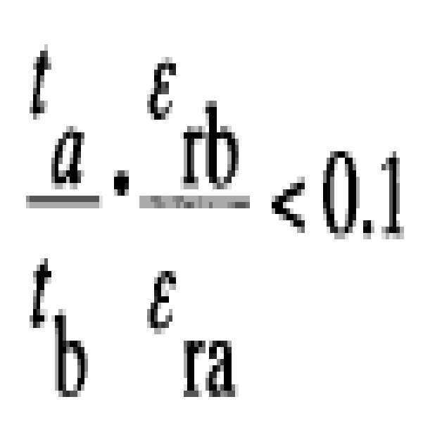
A first channel forming region; A first gate insulating layer on the first channel forming region; A first gate electrode overlying the first channel formation region and overlying the first gate insulation layer; And a source region and a drain region, the first channel forming region being interposed between the source region and the drain region;
A second channel forming region; A source electrode and a drain electrode electrically connected to the second channel formation region; A second gate electrode over the second channel formation region; And a second gate insulating layer between the second channel forming region and the second gate electrode,
The second channel forming region and an insulating layer between one of the source region and the drain region,
And a memory cell,
Wherein the first transistor and the second transistor overlap each other at least partially,
Wherein the second gate insulating layer and the insulating layer satisfy the following expression
제1 채널 형성 영역; 상기 제1 채널 형성 영역 위의 제1 게이트 절연층; 상기 제1 채널 형성 영역과 중첩하고, 상기 제1 게이트 절연층 위의 제1 게이트 전극; 및 소스 영역과 드레인 영역 - 상기 제1 채널 형성 영역이 상기 소스 영역과 상기 드레인 영역 사이에 개재됨 - 을 포함하는 제1 트랜지스터와,
제2 채널 형성 영역; 상기 제2 채널 형성 영역에 전기적으로 접속된 소스 전극과 드레인 전극; 상기 제2 채널 형성 영역 위의 제2 게이트 전극; 및 상기 제2 채널 형성 영역과 상기 제2 게이트 전극 사이의 제2 게이트 절연층을 포함하는 제2 트랜지스터와,
상기 제2 채널 형성 영역과, 상기 소스 영역과 상기 드레인 영역 중 하나 사이의 절연층
을 포함하는 메모리 셀을 포함하고,
상기 제1 트랜지스터와 상기 제2 트랜지스터가 적어도 부분적으로 서로 중첩하고,
상기 소스 전극의 일부와 상기 드레인 전극의 일부가 상기 제2 채널 형성 영역 위에 제공되고,
상기 제2 게이트 절연층과 상기 절연층이 수학식

A first channel forming region; A first gate insulating layer on the first channel forming region; A first gate electrode overlying the first channel formation region and overlying the first gate insulation layer; And a source region and a drain region, the first channel forming region being interposed between the source region and the drain region;
A second channel forming region; A source electrode and a drain electrode electrically connected to the second channel formation region; A second gate electrode over the second channel formation region; And a second gate insulating layer between the second channel forming region and the second gate electrode,
The second channel forming region and an insulating layer between one of the source region and the drain region,
And a memory cell,
Wherein the first transistor and the second transistor overlap each other at least partially,
A part of the source electrode and a part of the drain electrode are provided on the second channel forming region,
Wherein the second gate insulating layer and the insulating layer satisfy the following expression
상기 제1 게이트 전극이 상기 소스 전극과 상기 드레인 전극 중 하나에 전기적으로 접속된, 반도체 장치.4. The method according to any one of claims 1 to 3,
And the first gate electrode is electrically connected to one of the source electrode and the drain electrode.
상기 제2 게이트 절연층, 도전층, 및 상기 소스 전극과 상기 드레인 전극 중 하나에 의해 용량 소자가 구성되는, 반도체 장치.4. The method according to any one of claims 1 to 3,
Wherein the second gate insulating layer, the conductive layer, and one of the source electrode and the drain electrode constitute a capacitive element.
상기 제1 채널 형성 영역이 제1 반도체 재료를 포함하고,
상기 제2 채널 형성 영역이 제2 반도체 재료를 포함하고,
상기 제1 반도체 재료와 상기 제2 반도체 재료가 서로 다른, 반도체 장치.4. The method according to any one of claims 1 to 3,
Wherein the first channel formation region comprises a first semiconductor material,
Wherein the second channel formation region comprises a second semiconductor material,
Wherein the first semiconductor material and the second semiconductor material are different.
상기 제2 채널 형성 영역이 산화물 반도체를 포함하는, 반도체 장치.4. The method according to any one of claims 1 to 3,
And the second channel formation region includes an oxide semiconductor.
제1 트랜지스터;
상기 제1 트랜지스터의 소스 영역과 드레인 영역 중 하나 위의 절연층; 및
상기 절연층 위의 채널 형성 영역, 상기 채널 형성 영역 위의 게이트 절연층, 및 상기 게이트 절연층 위의 게이트 전극을 포함하는 제2 트랜지스터
를 포함하고,
상기 제1 트랜지스터의 게이트 전극의 상면은 상기 제2 트랜지스터의 소스 전극과 드레인 전극 중 하나의 하면과 접촉되고,
상기 제2 트랜지스터의 상기 게이트 절연층과 상기 절연층이 수학식

A first transistor;
An insulating layer over one of a source region and a drain region of the first transistor; And
A second transistor including a channel forming region on the insulating layer, a gate insulating layer on the channel forming region, and a gate electrode on the gate insulating layer,
Lt; / RTI >
The upper surface of the gate electrode of the first transistor is in contact with the lower surface of one of the source electrode and the drain electrode of the second transistor,
Wherein the gate insulating layer and the insulating layer of the second transistor satisfy Equation
제1 트랜지스터;
상기 제1 트랜지스터의 소스 영역과 드레인 영역 중 하나 위의 절연층; 및
상기 절연층 위의 채널 형성 영역, 상기 채널 형성 영역 위의 게이트 절연층, 및 상기 게이트 절연층 위의 게이트 전극을 포함하는 제2 트랜지스터
를 포함하고,
상기 제1 트랜지스터의 게이트 전극의 상면의 레벨은 상기 절연층의 상면의 레벨과 실질적으로 동일하고,
상기 제1 트랜지스터의 상기 게이트 전극은 상기 제2 트랜지스터의 소스 전극과 드레인 적극 중 하나에 전기적으로 접속되고,
상기 제2 트랜지스터의 상기 게이트 절연층과 상기 절연층이 수학식

A first transistor;
An insulating layer over one of a source region and a drain region of the first transistor; And
A second transistor including a channel forming region on the insulating layer, a gate insulating layer on the channel forming region, and a gate electrode on the gate insulating layer,
Lt; / RTI >
The level of the upper surface of the gate electrode of the first transistor is substantially equal to the level of the upper surface of the insulating layer,
The gate electrode of the first transistor is electrically connected to one of the source electrode and the drain electrode of the second transistor,
Wherein the gate insulating layer and the insulating layer of the second transistor satisfy Equation
상기 제2 트랜지스터의 상기 채널 형성 영역은 In-Ga-Zn-O-계의 산화물 반도체를 포함하는, 반도체 장치.10. The method according to claim 8 or 9,
And the channel forming region of the second transistor includes an In-Ga-Zn-O-based oxide semiconductor.
제1 트랜지스터;
상기 제1 트랜지스터의 소스 영역과 드레인 영역 중 하나 위의 절연층; 및
상기 절연층 위의 채널 형성 영역, 상기 채널 형성 영역 위의 게이트 절연층, 및 상기 게이트 절연층 위의 게이트 전극을 포함하는 제2 트랜지스터
를 포함하고,
상기 제1 트랜지스터의 게이트 전극의 상면은 상기 제2 트랜지스터의 소스 전극과 드레인 전극 중 하나의 하면과 접촉되고,
상기 제1 트랜지스터의 채널 형성 영역은 실리콘을 포함하고,
상기 제2 트랜지스터의 상기 채널 형성 영역은 산화물 반도체를 포함하고,
상기 제2 트랜지스터의 상기 게이트 절연층과 상기 절연층이 수학식

A first transistor;
An insulating layer over one of a source region and a drain region of the first transistor; And
A second transistor including a channel forming region on the insulating layer, a gate insulating layer on the channel forming region, and a gate electrode on the gate insulating layer,
Lt; / RTI >
The upper surface of the gate electrode of the first transistor is in contact with the lower surface of one of the source electrode and the drain electrode of the second transistor,
Wherein the channel forming region of the first transistor comprises silicon,
Wherein the channel forming region of the second transistor comprises an oxide semiconductor,
Wherein the gate insulating layer and the insulating layer of the second transistor satisfy Equation
상기 제1 트랜지스터의 상기 게이트 전극의 상기 상면은 상기 절연층이 화학 기계적 연마에 의해 형성될 때 노출되는, 반도체 장치.The method according to any one of claims 8, 9 and 11,
Wherein the upper surface of the gate electrode of the first transistor is exposed when the insulating layer is formed by chemical mechanical polishing.
상기 산화물 반도체는 In-Ga-Zn-O-계의 산화물 반도체인, 반도체 장치.12. The method of claim 11,
Wherein the oxide semiconductor is an In-Ga-Zn-O-based oxide semiconductor.
상기 제2 트랜지스터의 채널 폭의 1㎛당 오프 상태 전류는 25℃에서 100zA/㎛ 미만인, 반도체 장치.The method according to any one of claims 8, 9 and 11,
The off-state current per 1 mu m of the channel width of the second transistor is less than 100 zA / [mu] m at 25 [deg.] C.
메모리 셀은 상기 제1 트랜지스터와 상기 제2 트랜지스터를 포함하는, 반도체 장치.The method according to any one of claims 8, 9 and 11,
And the memory cell includes the first transistor and the second transistor.
상기 제2 트랜지스터의 상기 게이트 절연층은 화학양론적 조성비 초과의 비율로 산소를 포함하는, 반도체 장치.The method according to any one of claims 8, 9 and 11,
Wherein the gate insulator layer of the second transistor comprises oxygen at a ratio exceeding a stoichiometric compositional ratio.
상기 제2 트랜지스터의 상기 게이트 절연층의 상기 두께 ta는 30㎚ 이하이고, 상기 절연층의 상기 두께 tb는 90㎚ 이상인, 반도체 장치.The method according to any one of claims 8, 9 and 11,
The thickness t a of the gate insulating layer of the second transistor is 30 nm or less and the thickness t b of the insulating layer is 90 nm or more.
Applications Claiming Priority (3)
| Application Number | Priority Date | Filing Date | Title |
|---|---|---|---|
| JPJP-P-2010-162184 | 2010-07-16 | ||
| JP2010162184 | 2010-07-16 | ||
| PCT/JP2011/064856 WO2012008304A1 (en) | 2010-07-16 | 2011-06-22 | Semiconductor device |
Publications (2)
| Publication Number | Publication Date |
|---|---|
| KR20130043162A KR20130043162A (en) | 2013-04-29 |
| KR101850567B1 true KR101850567B1 (en) | 2018-04-19 |
Family
ID=45466225
Family Applications (1)
| Application Number | Title | Priority Date | Filing Date |
|---|---|---|---|
| KR1020137001409A KR101850567B1 (en) | 2010-07-16 | 2011-06-22 | Semiconductor device |
Country Status (6)
| Country | Link |
|---|---|
| US (2) | US8461586B2 (en) |
| JP (3) | JP5674576B2 (en) |
| KR (1) | KR101850567B1 (en) |
| CN (1) | CN103003934B (en) |
| TW (2) | TWI624931B (en) |
| WO (1) | WO2012008304A1 (en) |
Families Citing this family (25)
| Publication number | Priority date | Publication date | Assignee | Title |
|---|---|---|---|---|
| CN105655340B (en) | 2009-12-18 | 2020-01-21 | 株式会社半导体能源研究所 | Semiconductor device with a plurality of semiconductor chips |
| KR101853516B1 (en) * | 2010-07-27 | 2018-04-30 | 가부시키가이샤 한도오따이 에네루기 켄큐쇼 | Semiconductor device |
| US8422272B2 (en) | 2010-08-06 | 2013-04-16 | Semiconductor Energy Laboratory Co., Ltd. | Semiconductor device and driving method thereof |
| US8582348B2 (en) | 2010-08-06 | 2013-11-12 | Semiconductor Energy Laboratory Co., Ltd. | Semiconductor device and method for driving semiconductor device |
| KR101851817B1 (en) | 2010-09-03 | 2018-04-24 | 가부시키가이샤 한도오따이 에네루기 켄큐쇼 | Semiconductor device and driving method thereof |
| JP6013682B2 (en) | 2011-05-20 | 2016-10-25 | 株式会社半導体エネルギー研究所 | Driving method of semiconductor device |
| JP2013125826A (en) * | 2011-12-14 | 2013-06-24 | Renesas Electronics Corp | Semiconductor device and method of manufacturing the same |
| US9312257B2 (en) | 2012-02-29 | 2016-04-12 | Semiconductor Energy Laboratory Co., Ltd. | Semiconductor device |
| US9349849B2 (en) | 2012-03-28 | 2016-05-24 | Semiconductor Energy Laboratory Co., Ltd. | Semiconductor device and electronic device including the semiconductor device |
| JP2013229013A (en) * | 2012-03-29 | 2013-11-07 | Semiconductor Energy Lab Co Ltd | Array controller and storage system |
| KR102119914B1 (en) * | 2012-05-31 | 2020-06-05 | 가부시키가이샤 한도오따이 에네루기 켄큐쇼 | Semiconductor device and manufacturing method thereof |
| KR102113160B1 (en) * | 2012-06-15 | 2020-05-20 | 가부시키가이샤 한도오따이 에네루기 켄큐쇼 | Semiconductor device |
| KR102211215B1 (en) * | 2012-09-14 | 2021-02-02 | 가부시키가이샤 한도오따이 에네루기 켄큐쇼 | Semiconductor device and method for fabricating the same |
| KR20140100307A (en) * | 2013-02-06 | 2014-08-14 | 삼성디스플레이 주식회사 | Oranic light emitting transistor |
| JP6486712B2 (en) | 2014-04-30 | 2019-03-20 | 株式会社半導体エネルギー研究所 | Oxide semiconductor film |
| SG10201912585TA (en) | 2014-05-30 | 2020-02-27 | Semiconductor Energy Lab | Semiconductor device and method for manufacturing the same |
| US9831238B2 (en) | 2014-05-30 | 2017-11-28 | Semiconductor Energy Laboratory Co., Ltd. | Semiconductor device including insulating film having opening portion and conductive film in the opening portion |
| US9647129B2 (en) * | 2014-07-04 | 2017-05-09 | Semiconductor Energy Laboratory Co., Ltd. | Semiconductor device |
| US9705004B2 (en) | 2014-08-01 | 2017-07-11 | Semiconductor Energy Laboratory Co., Ltd. | Semiconductor device |
| DE102015106979B4 (en) * | 2015-05-05 | 2023-01-12 | Infineon Technologies Austria Ag | Semiconductor wafers and methods of manufacturing semiconductor devices in a semiconductor wafer |
| CN108140657A (en) * | 2015-09-30 | 2018-06-08 | 株式会社半导体能源研究所 | Semiconductor device and electronic equipment |
| FR3054920B1 (en) | 2016-08-05 | 2018-10-26 | Stmicroelectronics (Rousset) Sas | COMPACT NON-VOLATILE MEMORY DEVICE |
| US9871050B1 (en) * | 2016-08-10 | 2018-01-16 | Globalfoundries Inc. | Flash memory device |
| US10692869B2 (en) * | 2016-11-17 | 2020-06-23 | Semiconductor Energy Laboratory Co., Ltd. | Semiconductor device and method for manufacturing semiconductor device |
| US10043808B1 (en) * | 2017-03-16 | 2018-08-07 | Toshiba Memory Corporation | Semiconductor memory |
Citations (3)
| Publication number | Priority date | Publication date | Assignee | Title |
|---|---|---|---|---|
| JP2003197772A (en) | 2001-12-27 | 2003-07-11 | Sony Corp | Capacitor, semiconductor storage device and its manufacturing method |
| JP2009094492A (en) * | 2007-09-20 | 2009-04-30 | Semiconductor Energy Lab Co Ltd | Display device |
| US20100171199A1 (en) | 2007-08-01 | 2010-07-08 | Seiichi Uchida | Production method of semiconductor device, semiconductor device, and exposure apparatus |
Family Cites Families (152)
| Publication number | Priority date | Publication date | Assignee | Title |
|---|---|---|---|---|
| JPS6034199B2 (en) * | 1980-12-20 | 1985-08-07 | 株式会社東芝 | semiconductor storage device |
| DE3171836D1 (en) | 1980-12-08 | 1985-09-19 | Toshiba Kk | Semiconductor memory device |
| JPS6070760A (en) * | 1983-09-27 | 1985-04-22 | Fujitsu Ltd | Semiconductor memory device |
| JPS60198861A (en) | 1984-03-23 | 1985-10-08 | Fujitsu Ltd | Thin film transistor |
| JPH0244256B2 (en) | 1987-01-28 | 1990-10-03 | Kagaku Gijutsucho Mukizaishitsu Kenkyushocho | INGAZN2O5DESHIMESARERUROTSUHOSHOKEINOSOJOKOZOOJUSURUKAGOBUTSUOYOBISONOSEIZOHO |
| JPH0244260B2 (en) | 1987-02-24 | 1990-10-03 | Kagaku Gijutsucho Mukizaishitsu Kenkyushocho | INGAZN5O8DESHIMESARERUROTSUHOSHOKEINOSOJOKOZOOJUSURUKAGOBUTSUOYOBISONOSEIZOHO |
| JPS63210023A (en) | 1987-02-24 | 1988-08-31 | Natl Inst For Res In Inorg Mater | Compound having laminar structure of hexagonal crystal system expressed by ingazn4o7 and its production |
| JPH0244258B2 (en) | 1987-02-24 | 1990-10-03 | Kagaku Gijutsucho Mukizaishitsu Kenkyushocho | INGAZN3O6DESHIMESARERUROTSUHOSHOKEINOSOJOKOZOOJUSURUKAGOBUTSUOYOBISONOSEIZOHO |
| JPH0244262B2 (en) | 1987-02-27 | 1990-10-03 | Kagaku Gijutsucho Mukizaishitsu Kenkyushocho | INGAZN6O9DESHIMESARERUROTSUHOSHOKEINOSOJOKOZOOJUSURUKAGOBUTSUOYOBISONOSEIZOHO |
| JPH0244263B2 (en) | 1987-04-22 | 1990-10-03 | Kagaku Gijutsucho Mukizaishitsu Kenkyushocho | INGAZN7O10DESHIMESARERUROTSUHOSHOKEINOSOJOKOZOOJUSURUKAGOBUTSUOYOBISONOSEIZOHO |
| US5006913A (en) * | 1988-11-05 | 1991-04-09 | Mitsubishi Denki Kabushiki Kaisha | Stacked type semiconductor device |
| JP2775040B2 (en) | 1991-10-29 | 1998-07-09 | 株式会社 半導体エネルギー研究所 | Electro-optical display device and driving method thereof |
| JPH05251705A (en) | 1992-03-04 | 1993-09-28 | Fuji Xerox Co Ltd | Thin-film transistor |
| JPH07176184A (en) * | 1993-12-20 | 1995-07-14 | Mitsubishi Electric Corp | Semiconductor memory and writing and reading method for data in the semiconductor memory |
| US5612552A (en) * | 1994-03-31 | 1997-03-18 | Lsi Logic Corporation | Multilevel gate array integrated circuit structure with perpendicular access to all active device regions |
| JP3479375B2 (en) | 1995-03-27 | 2003-12-15 | 科学技術振興事業団 | Metal oxide semiconductor device in which a pn junction is formed with a thin film transistor made of a metal oxide semiconductor such as cuprous oxide, and methods for manufacturing the same |
| KR100394896B1 (en) | 1995-08-03 | 2003-11-28 | 코닌클리케 필립스 일렉트로닉스 엔.브이. | A semiconductor device including a transparent switching element |
| JP3625598B2 (en) | 1995-12-30 | 2005-03-02 | 三星電子株式会社 | Manufacturing method of liquid crystal display device |
| JP4103968B2 (en) | 1996-09-18 | 2008-06-18 | 株式会社半導体エネルギー研究所 | Insulated gate type semiconductor device |
| US6150695A (en) * | 1996-10-30 | 2000-11-21 | Advanced Micro Devices, Inc. | Multilevel transistor formation employing a local substrate formed within a shallow trench |
| US5926700A (en) * | 1997-05-02 | 1999-07-20 | Advanced Micro Devices, Inc. | Semiconductor fabrication having multi-level transistors and high density interconnect therebetween |
| US5818069A (en) * | 1997-06-20 | 1998-10-06 | Advanced Micro Devices, Inc. | Ultra high density series-connected transistors formed on separate elevational levels |
| JP4032454B2 (en) * | 1997-06-27 | 2008-01-16 | ソニー株式会社 | Manufacturing method of three-dimensional circuit element |
| US6392277B1 (en) * | 1997-11-21 | 2002-05-21 | Hitachi, Ltd. | Semiconductor device |
| JP4170454B2 (en) | 1998-07-24 | 2008-10-22 | Hoya株式会社 | Article having transparent conductive oxide thin film and method for producing the same |
| JP2000150861A (en) | 1998-11-16 | 2000-05-30 | Tdk Corp | Oxide thin film |
| JP3276930B2 (en) | 1998-11-17 | 2002-04-22 | 科学技術振興事業団 | Transistor and semiconductor device |
| JP2000269358A (en) * | 1999-03-17 | 2000-09-29 | Hitachi Ltd | Semiconductor device and method of producing the same |
| JP2001093988A (en) | 1999-07-22 | 2001-04-06 | Sony Corp | Semiconductor storage |
| JP4654471B2 (en) | 1999-07-29 | 2011-03-23 | ソニー株式会社 | Semiconductor device |
| JP2001053164A (en) | 1999-08-04 | 2001-02-23 | Sony Corp | Semiconductor storage device |
| TW460731B (en) | 1999-09-03 | 2001-10-21 | Ind Tech Res Inst | Electrode structure and production method of wide viewing angle LCD |
| JP2001168198A (en) | 1999-12-09 | 2001-06-22 | Sony Corp | Memory hybrid semiconductor integrated circuit and its design method |
| US6320228B1 (en) * | 2000-01-14 | 2001-11-20 | Advanced Micro Devices, Inc. | Multiple active layer integrated circuit and a method of making such a circuit |
| US6429484B1 (en) * | 2000-08-07 | 2002-08-06 | Advanced Micro Devices, Inc. | Multiple active layer structure and a method of making such a structure |
| JP4089858B2 (en) | 2000-09-01 | 2008-05-28 | 国立大学法人東北大学 | Semiconductor device |
| JP3749101B2 (en) * | 2000-09-14 | 2006-02-22 | 株式会社ルネサステクノロジ | Semiconductor device |
| KR20020038482A (en) | 2000-11-15 | 2002-05-23 | 모리시타 요이찌 | Thin film transistor array, method for producing the same, and display panel using the same |
| US6887753B2 (en) * | 2001-02-28 | 2005-05-03 | Micron Technology, Inc. | Methods of forming semiconductor circuitry, and semiconductor circuit constructions |
| JP3997731B2 (en) | 2001-03-19 | 2007-10-24 | 富士ゼロックス株式会社 | Method for forming a crystalline semiconductor thin film on a substrate |
| JP2002289859A (en) | 2001-03-23 | 2002-10-04 | Minolta Co Ltd | Thin-film transistor |
| JP2002368226A (en) * | 2001-06-11 | 2002-12-20 | Sharp Corp | Semiconductor device, semiconductor memory device and manufacturing method, and portable information equipment |
| JP3925839B2 (en) | 2001-09-10 | 2007-06-06 | シャープ株式会社 | Semiconductor memory device and test method thereof |
| JP4090716B2 (en) | 2001-09-10 | 2008-05-28 | 雅司 川崎 | Thin film transistor and matrix display device |
| EP1443130B1 (en) | 2001-11-05 | 2011-09-28 | Japan Science and Technology Agency | Natural superlattice homologous single crystal thin film, method for preparation thereof, and device using said single crystal thin film |
| JP4164562B2 (en) | 2002-09-11 | 2008-10-15 | 独立行政法人科学技術振興機構 | Transparent thin film field effect transistor using homologous thin film as active layer |
| JP4083486B2 (en) | 2002-02-21 | 2008-04-30 | 独立行政法人科学技術振興機構 | Method for producing LnCuO (S, Se, Te) single crystal thin film |
| CN1445821A (en) | 2002-03-15 | 2003-10-01 | 三洋电机株式会社 | Forming method of ZnO film and ZnO semiconductor layer, semiconductor element and manufacturing method thereof |
| JP3933591B2 (en) | 2002-03-26 | 2007-06-20 | 淳二 城戸 | Organic electroluminescent device |
| JP2003332582A (en) * | 2002-05-13 | 2003-11-21 | Toshiba Corp | Semiconductor device and its manufacturing method |
| US7339187B2 (en) | 2002-05-21 | 2008-03-04 | State Of Oregon Acting By And Through The Oregon State Board Of Higher Education On Behalf Of Oregon State University | Transistor structures |
| JP2004022625A (en) | 2002-06-13 | 2004-01-22 | Murata Mfg Co Ltd | Manufacturing method of semiconductor device and its manufacturing method |
| US7105868B2 (en) | 2002-06-24 | 2006-09-12 | Cermet, Inc. | High-electron mobility transistor with zinc oxide |
| US6882010B2 (en) * | 2002-10-03 | 2005-04-19 | Micron Technology, Inc. | High performance three-dimensional TFT-based CMOS inverters, and computer systems utilizing such novel CMOS inverters |
| US7067843B2 (en) | 2002-10-11 | 2006-06-27 | E. I. Du Pont De Nemours And Company | Transparent oxide semiconductor thin film transistors |
| JP4166105B2 (en) | 2003-03-06 | 2008-10-15 | シャープ株式会社 | Semiconductor device and manufacturing method thereof |
| JP2004273732A (en) | 2003-03-07 | 2004-09-30 | Sharp Corp | Active matrix substrate and its producing process |
| US7183611B2 (en) * | 2003-06-03 | 2007-02-27 | Micron Technology, Inc. | SRAM constructions, and electronic systems comprising SRAM constructions |
| JP4108633B2 (en) | 2003-06-20 | 2008-06-25 | シャープ株式会社 | THIN FILM TRANSISTOR, MANUFACTURING METHOD THEREOF, AND ELECTRONIC DEVICE |
| US7262463B2 (en) | 2003-07-25 | 2007-08-28 | Hewlett-Packard Development Company, L.P. | Transistor including a deposited channel region having a doped portion |
| US8445946B2 (en) | 2003-12-11 | 2013-05-21 | International Business Machines Corporation | Gated diode memory cells |
| US7297977B2 (en) | 2004-03-12 | 2007-11-20 | Hewlett-Packard Development Company, L.P. | Semiconductor device |
| US7282782B2 (en) | 2004-03-12 | 2007-10-16 | Hewlett-Packard Development Company, L.P. | Combined binary oxide semiconductor device |
| US7145174B2 (en) | 2004-03-12 | 2006-12-05 | Hewlett-Packard Development Company, Lp. | Semiconductor device |
| EP2413366B1 (en) | 2004-03-12 | 2017-01-11 | Japan Science And Technology Agency | A switching element of LCDs or organic EL displays |
| US7211825B2 (en) | 2004-06-14 | 2007-05-01 | Yi-Chi Shih | Indium oxide-based thin film transistors and circuits |
| JP2006041365A (en) * | 2004-07-29 | 2006-02-09 | Toshiba Corp | Semiconductor memory, and manufacturing method thereof |
| JP2006100760A (en) | 2004-09-02 | 2006-04-13 | Casio Comput Co Ltd | Thin-film transistor and its manufacturing method |
| US7285501B2 (en) | 2004-09-17 | 2007-10-23 | Hewlett-Packard Development Company, L.P. | Method of forming a solution processed device |
| US7298084B2 (en) | 2004-11-02 | 2007-11-20 | 3M Innovative Properties Company | Methods and displays utilizing integrated zinc oxide row and column drivers in conjunction with organic light emitting diodes |
| CN101057338B (en) | 2004-11-10 | 2011-03-16 | 佳能株式会社 | Field effect transistor employing an amorphous oxide |
| US7791072B2 (en) | 2004-11-10 | 2010-09-07 | Canon Kabushiki Kaisha | Display |
| KR100953596B1 (en) | 2004-11-10 | 2010-04-21 | 캐논 가부시끼가이샤 | Light-emitting device |
| US7829444B2 (en) | 2004-11-10 | 2010-11-09 | Canon Kabushiki Kaisha | Field effect transistor manufacturing method |
| US7863611B2 (en) | 2004-11-10 | 2011-01-04 | Canon Kabushiki Kaisha | Integrated circuits utilizing amorphous oxides |
| US7453065B2 (en) | 2004-11-10 | 2008-11-18 | Canon Kabushiki Kaisha | Sensor and image pickup device |
| CN101057339B (en) | 2004-11-10 | 2012-12-26 | 佳能株式会社 | Amorphous oxide and field effect transistor |
| CN100541803C (en) * | 2004-11-11 | 2009-09-16 | 株式会社半导体能源研究所 | Semiconductor device |
| US7579224B2 (en) | 2005-01-21 | 2009-08-25 | Semiconductor Energy Laboratory Co., Ltd. | Method for manufacturing a thin film semiconductor device |
| TWI569441B (en) | 2005-01-28 | 2017-02-01 | 半導體能源研究所股份有限公司 | Semiconductor device, electronic device, and method of manufacturing semiconductor device |
| TWI472037B (en) | 2005-01-28 | 2015-02-01 | Semiconductor Energy Lab | Semiconductor device, electronic device, and method of manufacturing semiconductor device |
| US7858451B2 (en) | 2005-02-03 | 2010-12-28 | Semiconductor Energy Laboratory Co., Ltd. | Electronic device, semiconductor device and manufacturing method thereof |
| US7948171B2 (en) | 2005-02-18 | 2011-05-24 | Semiconductor Energy Laboratory Co., Ltd. | Light emitting device |
| US20060197092A1 (en) | 2005-03-03 | 2006-09-07 | Randy Hoffman | System and method for forming conductive material on a substrate |
| US8681077B2 (en) | 2005-03-18 | 2014-03-25 | Semiconductor Energy Laboratory Co., Ltd. | Semiconductor device, and display device, driving method and electronic apparatus thereof |
| WO2006105077A2 (en) | 2005-03-28 | 2006-10-05 | Massachusetts Institute Of Technology | Low voltage thin film transistor with high-k dielectric material |
| US7645478B2 (en) | 2005-03-31 | 2010-01-12 | 3M Innovative Properties Company | Methods of making displays |
| JP4849817B2 (en) | 2005-04-08 | 2012-01-11 | ルネサスエレクトロニクス株式会社 | Semiconductor memory device |
| KR100621633B1 (en) * | 2005-04-18 | 2006-09-19 | 삼성전자주식회사 | Method of forming a semiconductor device having stacked transisters and the device so formed |
| KR100684894B1 (en) * | 2005-04-18 | 2007-02-20 | 삼성전자주식회사 | Method of forming a semiconductor device having stacked transisters |
| US8300031B2 (en) | 2005-04-20 | 2012-10-30 | Semiconductor Energy Laboratory Co., Ltd. | Semiconductor device comprising transistor having gate and drain connected through a current-voltage conversion element |
| JP2006344849A (en) | 2005-06-10 | 2006-12-21 | Casio Comput Co Ltd | Thin film transistor |
| US7691666B2 (en) | 2005-06-16 | 2010-04-06 | Eastman Kodak Company | Methods of making thin film transistors comprising zinc-oxide-based semiconductor materials and transistors made thereby |
| US7402506B2 (en) | 2005-06-16 | 2008-07-22 | Eastman Kodak Company | Methods of making thin film transistors comprising zinc-oxide-based semiconductor materials and transistors made thereby |
| US7507618B2 (en) | 2005-06-27 | 2009-03-24 | 3M Innovative Properties Company | Method for making electronic devices using metal oxide nanoparticles |
| KR100711890B1 (en) | 2005-07-28 | 2007-04-25 | 삼성에스디아이 주식회사 | Organic Light Emitting Display and Fabrication Method for the same |
| JP2007059128A (en) | 2005-08-23 | 2007-03-08 | Canon Inc | Organic electroluminescent display device and manufacturing method thereof |
| JP5116225B2 (en) | 2005-09-06 | 2013-01-09 | キヤノン株式会社 | Manufacturing method of oxide semiconductor device |
| JP4850457B2 (en) | 2005-09-06 | 2012-01-11 | キヤノン株式会社 | Thin film transistor and thin film diode |
| JP2007073705A (en) | 2005-09-06 | 2007-03-22 | Canon Inc | Oxide-semiconductor channel film transistor and its method of manufacturing same |
| JP4280736B2 (en) | 2005-09-06 | 2009-06-17 | キヤノン株式会社 | Semiconductor element |
| EP3614442A3 (en) | 2005-09-29 | 2020-03-25 | Semiconductor Energy Laboratory Co., Ltd. | Semiconductor device having oxide semiconductor layer and manufactoring method thereof |
| JP5037808B2 (en) | 2005-10-20 | 2012-10-03 | キヤノン株式会社 | Field effect transistor using amorphous oxide, and display device using the transistor |
| KR20090115222A (en) | 2005-11-15 | 2009-11-04 | 가부시키가이샤 한도오따이 에네루기 켄큐쇼 | Manufacturing method of semiconductor device |
| TWI292281B (en) | 2005-12-29 | 2008-01-01 | Ind Tech Res Inst | Pixel structure of active organic light emitting diode and method of fabricating the same |
| US7867636B2 (en) | 2006-01-11 | 2011-01-11 | Murata Manufacturing Co., Ltd. | Transparent conductive film and method for manufacturing the same |
| JP4977478B2 (en) | 2006-01-21 | 2012-07-18 | 三星電子株式会社 | ZnO film and method of manufacturing TFT using the same |
| US7576394B2 (en) | 2006-02-02 | 2009-08-18 | Kochi Industrial Promotion Center | Thin film transistor including low resistance conductive thin films and manufacturing method thereof |
| KR100714401B1 (en) * | 2006-02-08 | 2007-05-04 | 삼성전자주식회사 | Semiconductor device having stacked transistors and method of forming the same |
| US7977169B2 (en) | 2006-02-15 | 2011-07-12 | Kochi Industrial Promotion Center | Semiconductor device including active layer made of zinc oxide with controlled orientations and manufacturing method thereof |
| US8008137B2 (en) | 2006-03-15 | 2011-08-30 | Marvell World Trade Ltd. | Method for fabricating 1T-DRAM on bulk silicon |
| KR20070101595A (en) | 2006-04-11 | 2007-10-17 | 삼성전자주식회사 | Zno thin film transistor |
| US20070252928A1 (en) | 2006-04-28 | 2007-11-01 | Toppan Printing Co., Ltd. | Structure, transmission type liquid crystal display, reflection type display and manufacturing method thereof |
| JP5028033B2 (en) | 2006-06-13 | 2012-09-19 | キヤノン株式会社 | Oxide semiconductor film dry etching method |
| JP4999400B2 (en) | 2006-08-09 | 2012-08-15 | キヤノン株式会社 | Oxide semiconductor film dry etching method |
| JP4609797B2 (en) | 2006-08-09 | 2011-01-12 | Nec液晶テクノロジー株式会社 | Thin film device and manufacturing method thereof |
| JP4332545B2 (en) | 2006-09-15 | 2009-09-16 | キヤノン株式会社 | Field effect transistor and manufacturing method thereof |
| JP5164357B2 (en) | 2006-09-27 | 2013-03-21 | キヤノン株式会社 | Semiconductor device and manufacturing method of semiconductor device |
| JP4274219B2 (en) | 2006-09-27 | 2009-06-03 | セイコーエプソン株式会社 | Electronic devices, organic electroluminescence devices, organic thin film semiconductor devices |
| US7622371B2 (en) | 2006-10-10 | 2009-11-24 | Hewlett-Packard Development Company, L.P. | Fused nanocrystal thin film semiconductor and method |
| US7772021B2 (en) | 2006-11-29 | 2010-08-10 | Samsung Electronics Co., Ltd. | Flat panel displays comprising a thin-film transistor having a semiconductive oxide in its channel and methods of fabricating the same for use in flat panel displays |
| JP2008140684A (en) | 2006-12-04 | 2008-06-19 | Toppan Printing Co Ltd | Color el display, and its manufacturing method |
| KR101303578B1 (en) | 2007-01-05 | 2013-09-09 | 삼성전자주식회사 | Etching method of thin film |
| US8207063B2 (en) | 2007-01-26 | 2012-06-26 | Eastman Kodak Company | Process for atomic layer deposition |
| KR100851215B1 (en) | 2007-03-14 | 2008-08-07 | 삼성에스디아이 주식회사 | Thin film transistor and organic light-emitting dislplay device having the thin film transistor |
| JP2008276211A (en) * | 2007-04-05 | 2008-11-13 | Fujifilm Corp | Organic electroluminescent display device and patterning method |
| US7795613B2 (en) | 2007-04-17 | 2010-09-14 | Toppan Printing Co., Ltd. | Structure with transistor |
| KR101325053B1 (en) | 2007-04-18 | 2013-11-05 | 삼성디스플레이 주식회사 | Thin film transistor substrate and manufacturing method thereof |
| KR20080094300A (en) | 2007-04-19 | 2008-10-23 | 삼성전자주식회사 | Thin film transistor and method of manufacturing the same and flat panel display comprising the same |
| KR101334181B1 (en) | 2007-04-20 | 2013-11-28 | 삼성전자주식회사 | Thin Film Transistor having selectively crystallized channel layer and method of manufacturing the same |
| CN101663762B (en) | 2007-04-25 | 2011-09-21 | 佳能株式会社 | Oxynitride semiconductor |
| KR101345376B1 (en) | 2007-05-29 | 2013-12-24 | 삼성전자주식회사 | Fabrication method of ZnO family Thin film transistor |
| US8354674B2 (en) | 2007-06-29 | 2013-01-15 | Semiconductor Energy Laboratory Co., Ltd. | Semiconductor device wherein a property of a first semiconductor layer is different from a property of a second semiconductor layer |
| JP5366517B2 (en) * | 2007-12-03 | 2013-12-11 | 株式会社半導体エネルギー研究所 | Method for manufacturing semiconductor device |
| JP5215158B2 (en) | 2007-12-17 | 2013-06-19 | 富士フイルム株式会社 | Inorganic crystalline alignment film, method for manufacturing the same, and semiconductor device |
| JP5121478B2 (en) | 2008-01-31 | 2013-01-16 | 株式会社ジャパンディスプレイウェスト | Optical sensor element, imaging device, electronic device, and memory element |
| JP2009253204A (en) * | 2008-04-10 | 2009-10-29 | Idemitsu Kosan Co Ltd | Field-effect transistor using oxide semiconductor, and its manufacturing method |
| JP5480554B2 (en) | 2008-08-08 | 2014-04-23 | 株式会社半導体エネルギー研究所 | Semiconductor device |
| JP2010074137A (en) * | 2008-08-19 | 2010-04-02 | Fujifilm Corp | Imaging apparatus |
| JP4623179B2 (en) | 2008-09-18 | 2011-02-02 | ソニー株式会社 | Thin film transistor and manufacturing method thereof |
| JP5451280B2 (en) | 2008-10-09 | 2014-03-26 | キヤノン株式会社 | Wurtzite crystal growth substrate, manufacturing method thereof, and semiconductor device |
| US8445903B2 (en) * | 2008-10-23 | 2013-05-21 | Idemitsu Kosan Co., Ltd. | Thin film transistor having a crystalline semiconductor film including indium oxide which contains a hydrogen element and method for manufacturing same |
| JP5781720B2 (en) | 2008-12-15 | 2015-09-24 | ルネサスエレクトロニクス株式会社 | Semiconductor device and manufacturing method of semiconductor device |
| SG10201406869QA (en) | 2009-10-29 | 2014-12-30 | Semiconductor Energy Lab | Semiconductor device |
| KR101761432B1 (en) * | 2009-11-06 | 2017-07-25 | 가부시키가이샤 한도오따이 에네루기 켄큐쇼 | Semiconductor device |
| EP2887395B1 (en) | 2009-11-20 | 2019-05-08 | Semiconductor Energy Laboratory Co., Ltd. | Nonvolatile latch circuit and logic circuit, and semiconductor device using the same |
| KR20190124813A (en) * | 2009-11-20 | 2019-11-05 | 가부시키가이샤 한도오따이 에네루기 켄큐쇼 | Semiconductor device |
| WO2011065183A1 (en) | 2009-11-24 | 2011-06-03 | Semiconductor Energy Laboratory Co., Ltd. | Semiconductor device including memory cell |
| KR101803254B1 (en) | 2009-11-27 | 2017-11-30 | 가부시키가이샤 한도오따이 에네루기 켄큐쇼 | Semiconductor device |
| TWM381174U (en) * | 2010-01-11 | 2010-05-21 | Tpv Electronics Fujian Co Ltd | Heat dissipating structure for chip and monitor |
| WO2011105310A1 (en) | 2010-02-26 | 2011-09-01 | Semiconductor Energy Laboratory Co., Ltd. | Semiconductor device |
| WO2012002186A1 (en) * | 2010-07-02 | 2012-01-05 | Semiconductor Energy Laboratory Co., Ltd. | Semiconductor device |
-
2011
- 2011-06-22 CN CN201180034897.4A patent/CN103003934B/en not_active Expired - Fee Related
- 2011-06-22 KR KR1020137001409A patent/KR101850567B1/en active IP Right Grant
- 2011-06-22 WO PCT/JP2011/064856 patent/WO2012008304A1/en active Application Filing
- 2011-07-01 US US13/175,542 patent/US8461586B2/en active Active
- 2011-07-06 TW TW105123240A patent/TWI624931B/en not_active IP Right Cessation
- 2011-07-06 TW TW100123846A patent/TWI555175B/en not_active IP Right Cessation
- 2011-07-12 JP JP2011153615A patent/JP5674576B2/en not_active Expired - Fee Related
-
2013
- 2013-06-10 US US13/913,591 patent/US8847326B2/en not_active Expired - Fee Related
-
2014
- 2014-12-22 JP JP2014258245A patent/JP5950992B2/en active Active
-
2016
- 2016-06-07 JP JP2016113319A patent/JP6116737B2/en active Active
Patent Citations (3)
| Publication number | Priority date | Publication date | Assignee | Title |
|---|---|---|---|---|
| JP2003197772A (en) | 2001-12-27 | 2003-07-11 | Sony Corp | Capacitor, semiconductor storage device and its manufacturing method |
| US20100171199A1 (en) | 2007-08-01 | 2010-07-08 | Seiichi Uchida | Production method of semiconductor device, semiconductor device, and exposure apparatus |
| JP2009094492A (en) * | 2007-09-20 | 2009-04-30 | Semiconductor Energy Lab Co Ltd | Display device |
Also Published As
| Publication number | Publication date |
|---|---|
| US8461586B2 (en) | 2013-06-11 |
| JP2016195260A (en) | 2016-11-17 |
| JP2012039101A (en) | 2012-02-23 |
| JP5950992B2 (en) | 2016-07-13 |
| US20130341615A1 (en) | 2013-12-26 |
| CN103003934A (en) | 2013-03-27 |
| KR20130043162A (en) | 2013-04-29 |
| TW201205781A (en) | 2012-02-01 |
| US20120012837A1 (en) | 2012-01-19 |
| JP5674576B2 (en) | 2015-02-25 |
| JP2015111681A (en) | 2015-06-18 |
| US8847326B2 (en) | 2014-09-30 |
| JP6116737B2 (en) | 2017-04-19 |
| WO2012008304A1 (en) | 2012-01-19 |
| TWI555175B (en) | 2016-10-21 |
| TWI624931B (en) | 2018-05-21 |
| TW201639120A (en) | 2016-11-01 |
| CN103003934B (en) | 2015-07-01 |
Similar Documents
| Publication | Publication Date | Title |
|---|---|---|
| KR101850567B1 (en) | Semiconductor device | |
| JP6934912B2 (en) | Semiconductor device | |
| KR101904445B1 (en) | Semiconductor device | |
| KR101868140B1 (en) | Semiconductor device | |
| KR101775180B1 (en) | Semiconductor device and method for driving the same | |
| KR101760537B1 (en) | Semiconductor device | |
| KR101791279B1 (en) | Semiconductor device | |
| JP6293085B2 (en) | Semiconductor device | |
| JP5694045B2 (en) | Semiconductor device | |
| WO2011065258A1 (en) | Semiconductor device | |
| WO2011152233A1 (en) | Semiconductor device |
Legal Events
| Date | Code | Title | Description |
|---|---|---|---|
| A201 | Request for examination | ||
| E902 | Notification of reason for refusal | ||
| E701 | Decision to grant or registration of patent right |