JP7650293B2 - 半導体パッケージ構造及び製造方法 - Google Patents
半導体パッケージ構造及び製造方法 Download PDFInfo
- Publication number
- JP7650293B2 JP7650293B2 JP2022566266A JP2022566266A JP7650293B2 JP 7650293 B2 JP7650293 B2 JP 7650293B2 JP 2022566266 A JP2022566266 A JP 2022566266A JP 2022566266 A JP2022566266 A JP 2022566266A JP 7650293 B2 JP7650293 B2 JP 7650293B2
- Authority
- JP
- Japan
- Prior art keywords
- chip
- package structure
- substrate
- layer
- chip stack
- Prior art date
- Legal status (The legal status is an assumption and is not a legal conclusion. Google has not performed a legal analysis and makes no representation as to the accuracy of the status listed.)
- Active
Links
Images


Classifications
-
- H—ELECTRICITY
- H01—ELECTRIC ELEMENTS
- H01L—SEMICONDUCTOR DEVICES NOT COVERED BY CLASS H10
- H01L25/00—Assemblies consisting of a plurality of semiconductor or other solid state devices
- H01L25/18—Assemblies consisting of a plurality of semiconductor or other solid state devices the devices being of the types provided for in two or more different main groups of the same subclass of H10B, H10D, H10F, H10H, H10K or H10N
-
- H—ELECTRICITY
- H01—ELECTRIC ELEMENTS
- H01L—SEMICONDUCTOR DEVICES NOT COVERED BY CLASS H10
- H01L23/00—Details of semiconductor or other solid state devices
- H01L23/52—Arrangements for conducting electric current within the device in operation from one component to another, i.e. interconnections, e.g. wires, lead frames
- H01L23/538—Arrangements for conducting electric current within the device in operation from one component to another, i.e. interconnections, e.g. wires, lead frames the interconnection structure between a plurality of semiconductor chips being formed on, or in, insulating substrates
- H01L23/5385—Assembly of a plurality of insulating substrates
-
- H—ELECTRICITY
- H01—ELECTRIC ELEMENTS
- H01L—SEMICONDUCTOR DEVICES NOT COVERED BY CLASS H10
- H01L21/00—Processes or apparatus adapted for the manufacture or treatment of semiconductor or solid state devices or of parts thereof
- H01L21/02—Manufacture or treatment of semiconductor devices or of parts thereof
- H01L21/04—Manufacture or treatment of semiconductor devices or of parts thereof the devices having potential barriers, e.g. a PN junction, depletion layer or carrier concentration layer
- H01L21/50—Assembly of semiconductor devices using processes or apparatus not provided for in a single one of the groups H01L21/18 - H01L21/326 or H10D48/04 - H10D48/07 e.g. sealing of a cap to a base of a container
- H01L21/56—Encapsulations, e.g. encapsulation layers, coatings
- H01L21/563—Encapsulation of active face of flip-chip device, e.g. underfilling or underencapsulation of flip-chip, encapsulation preform on chip or mounting substrate
-
- H—ELECTRICITY
- H01—ELECTRIC ELEMENTS
- H01L—SEMICONDUCTOR DEVICES NOT COVERED BY CLASS H10
- H01L23/00—Details of semiconductor or other solid state devices
- H01L23/28—Encapsulations, e.g. encapsulating layers, coatings, e.g. for protection
- H01L23/29—Encapsulations, e.g. encapsulating layers, coatings, e.g. for protection characterised by the material, e.g. carbon
- H01L23/293—Organic, e.g. plastic
- H01L23/296—Organo-silicon compounds
-
- H—ELECTRICITY
- H01—ELECTRIC ELEMENTS
- H01L—SEMICONDUCTOR DEVICES NOT COVERED BY CLASS H10
- H01L23/00—Details of semiconductor or other solid state devices
- H01L23/28—Encapsulations, e.g. encapsulating layers, coatings, e.g. for protection
- H01L23/31—Encapsulations, e.g. encapsulating layers, coatings, e.g. for protection characterised by the arrangement or shape
- H01L23/3107—Encapsulations, e.g. encapsulating layers, coatings, e.g. for protection characterised by the arrangement or shape the device being completely enclosed
- H01L23/3121—Encapsulations, e.g. encapsulating layers, coatings, e.g. for protection characterised by the arrangement or shape the device being completely enclosed a substrate forming part of the encapsulation
- H01L23/3128—Encapsulations, e.g. encapsulating layers, coatings, e.g. for protection characterised by the arrangement or shape the device being completely enclosed a substrate forming part of the encapsulation the substrate having spherical bumps for external connection
-
- H—ELECTRICITY
- H01—ELECTRIC ELEMENTS
- H01L—SEMICONDUCTOR DEVICES NOT COVERED BY CLASS H10
- H01L23/00—Details of semiconductor or other solid state devices
- H01L23/28—Encapsulations, e.g. encapsulating layers, coatings, e.g. for protection
- H01L23/31—Encapsulations, e.g. encapsulating layers, coatings, e.g. for protection characterised by the arrangement or shape
- H01L23/3157—Partial encapsulation or coating
-
- H—ELECTRICITY
- H01—ELECTRIC ELEMENTS
- H01L—SEMICONDUCTOR DEVICES NOT COVERED BY CLASS H10
- H01L23/00—Details of semiconductor or other solid state devices
- H01L23/34—Arrangements for cooling, heating, ventilating or temperature compensation ; Temperature sensing arrangements
- H01L23/36—Selection of materials, or shaping, to facilitate cooling or heating, e.g. heatsinks
-
- H—ELECTRICITY
- H01—ELECTRIC ELEMENTS
- H01L—SEMICONDUCTOR DEVICES NOT COVERED BY CLASS H10
- H01L23/00—Details of semiconductor or other solid state devices
- H01L23/34—Arrangements for cooling, heating, ventilating or temperature compensation ; Temperature sensing arrangements
- H01L23/42—Fillings or auxiliary members in containers or encapsulations selected or arranged to facilitate heating or cooling
-
- H—ELECTRICITY
- H01—ELECTRIC ELEMENTS
- H01L—SEMICONDUCTOR DEVICES NOT COVERED BY CLASS H10
- H01L23/00—Details of semiconductor or other solid state devices
- H01L23/52—Arrangements for conducting electric current within the device in operation from one component to another, i.e. interconnections, e.g. wires, lead frames
- H01L23/538—Arrangements for conducting electric current within the device in operation from one component to another, i.e. interconnections, e.g. wires, lead frames the interconnection structure between a plurality of semiconductor chips being formed on, or in, insulating substrates
- H01L23/5383—Multilayer substrates
-
- H—ELECTRICITY
- H01—ELECTRIC ELEMENTS
- H01L—SEMICONDUCTOR DEVICES NOT COVERED BY CLASS H10
- H01L23/00—Details of semiconductor or other solid state devices
- H01L23/52—Arrangements for conducting electric current within the device in operation from one component to another, i.e. interconnections, e.g. wires, lead frames
- H01L23/538—Arrangements for conducting electric current within the device in operation from one component to another, i.e. interconnections, e.g. wires, lead frames the interconnection structure between a plurality of semiconductor chips being formed on, or in, insulating substrates
- H01L23/5384—Conductive vias through the substrate with or without pins, e.g. buried coaxial conductors
-
- H—ELECTRICITY
- H01—ELECTRIC ELEMENTS
- H01L—SEMICONDUCTOR DEVICES NOT COVERED BY CLASS H10
- H01L23/00—Details of semiconductor or other solid state devices
- H01L23/52—Arrangements for conducting electric current within the device in operation from one component to another, i.e. interconnections, e.g. wires, lead frames
- H01L23/538—Arrangements for conducting electric current within the device in operation from one component to another, i.e. interconnections, e.g. wires, lead frames the interconnection structure between a plurality of semiconductor chips being formed on, or in, insulating substrates
- H01L23/5386—Geometry or layout of the interconnection structure
-
- H—ELECTRICITY
- H01—ELECTRIC ELEMENTS
- H01L—SEMICONDUCTOR DEVICES NOT COVERED BY CLASS H10
- H01L24/00—Arrangements for connecting or disconnecting semiconductor or solid-state bodies; Methods or apparatus related thereto
- H01L24/01—Means for bonding being attached to, or being formed on, the surface to be connected, e.g. chip-to-package, die-attach, "first-level" interconnects; Manufacturing methods related thereto
- H01L24/02—Bonding areas ; Manufacturing methods related thereto
- H01L24/07—Structure, shape, material or disposition of the bonding areas after the connecting process
-
- H—ELECTRICITY
- H01—ELECTRIC ELEMENTS
- H01L—SEMICONDUCTOR DEVICES NOT COVERED BY CLASS H10
- H01L24/00—Arrangements for connecting or disconnecting semiconductor or solid-state bodies; Methods or apparatus related thereto
- H01L24/01—Means for bonding being attached to, or being formed on, the surface to be connected, e.g. chip-to-package, die-attach, "first-level" interconnects; Manufacturing methods related thereto
- H01L24/26—Layer connectors, e.g. plate connectors, solder or adhesive layers; Manufacturing methods related thereto
- H01L24/31—Structure, shape, material or disposition of the layer connectors after the connecting process
- H01L24/32—Structure, shape, material or disposition of the layer connectors after the connecting process of an individual layer connector
-
- H—ELECTRICITY
- H01—ELECTRIC ELEMENTS
- H01L—SEMICONDUCTOR DEVICES NOT COVERED BY CLASS H10
- H01L24/00—Arrangements for connecting or disconnecting semiconductor or solid-state bodies; Methods or apparatus related thereto
- H01L24/01—Means for bonding being attached to, or being formed on, the surface to be connected, e.g. chip-to-package, die-attach, "first-level" interconnects; Manufacturing methods related thereto
- H01L24/42—Wire connectors; Manufacturing methods related thereto
- H01L24/47—Structure, shape, material or disposition of the wire connectors after the connecting process
- H01L24/48—Structure, shape, material or disposition of the wire connectors after the connecting process of an individual wire connector
-
- H—ELECTRICITY
- H01—ELECTRIC ELEMENTS
- H01L—SEMICONDUCTOR DEVICES NOT COVERED BY CLASS H10
- H01L24/00—Arrangements for connecting or disconnecting semiconductor or solid-state bodies; Methods or apparatus related thereto
- H01L24/01—Means for bonding being attached to, or being formed on, the surface to be connected, e.g. chip-to-package, die-attach, "first-level" interconnects; Manufacturing methods related thereto
- H01L24/42—Wire connectors; Manufacturing methods related thereto
- H01L24/47—Structure, shape, material or disposition of the wire connectors after the connecting process
- H01L24/49—Structure, shape, material or disposition of the wire connectors after the connecting process of a plurality of wire connectors
-
- H—ELECTRICITY
- H01—ELECTRIC ELEMENTS
- H01L—SEMICONDUCTOR DEVICES NOT COVERED BY CLASS H10
- H01L24/00—Arrangements for connecting or disconnecting semiconductor or solid-state bodies; Methods or apparatus related thereto
- H01L24/73—Means for bonding being of different types provided for in two or more of groups H01L24/10, H01L24/18, H01L24/26, H01L24/34, H01L24/42, H01L24/50, H01L24/63, H01L24/71
-
- H—ELECTRICITY
- H01—ELECTRIC ELEMENTS
- H01L—SEMICONDUCTOR DEVICES NOT COVERED BY CLASS H10
- H01L24/00—Arrangements for connecting or disconnecting semiconductor or solid-state bodies; Methods or apparatus related thereto
- H01L24/91—Methods for connecting semiconductor or solid state bodies including different methods provided for in two or more of groups H01L24/80 - H01L24/90
- H01L24/92—Specific sequence of method steps
-
- H—ELECTRICITY
- H01—ELECTRIC ELEMENTS
- H01L—SEMICONDUCTOR DEVICES NOT COVERED BY CLASS H10
- H01L25/00—Assemblies consisting of a plurality of semiconductor or other solid state devices
- H01L25/03—Assemblies consisting of a plurality of semiconductor or other solid state devices all the devices being of a type provided for in a single subclass of subclasses H10B, H10D, H10F, H10H, H10K or H10N, e.g. assemblies of rectifier diodes
- H01L25/04—Assemblies consisting of a plurality of semiconductor or other solid state devices all the devices being of a type provided for in a single subclass of subclasses H10B, H10D, H10F, H10H, H10K or H10N, e.g. assemblies of rectifier diodes the devices not having separate containers
- H01L25/065—Assemblies consisting of a plurality of semiconductor or other solid state devices all the devices being of a type provided for in a single subclass of subclasses H10B, H10D, H10F, H10H, H10K or H10N, e.g. assemblies of rectifier diodes the devices not having separate containers the devices being of a type provided for in group H10D89/00
- H01L25/0652—Assemblies consisting of a plurality of semiconductor or other solid state devices all the devices being of a type provided for in a single subclass of subclasses H10B, H10D, H10F, H10H, H10K or H10N, e.g. assemblies of rectifier diodes the devices not having separate containers the devices being of a type provided for in group H10D89/00 the devices being arranged next and on each other, i.e. mixed assemblies
-
- H—ELECTRICITY
- H01—ELECTRIC ELEMENTS
- H01L—SEMICONDUCTOR DEVICES NOT COVERED BY CLASS H10
- H01L25/00—Assemblies consisting of a plurality of semiconductor or other solid state devices
- H01L25/03—Assemblies consisting of a plurality of semiconductor or other solid state devices all the devices being of a type provided for in a single subclass of subclasses H10B, H10D, H10F, H10H, H10K or H10N, e.g. assemblies of rectifier diodes
- H01L25/10—Assemblies consisting of a plurality of semiconductor or other solid state devices all the devices being of a type provided for in a single subclass of subclasses H10B, H10D, H10F, H10H, H10K or H10N, e.g. assemblies of rectifier diodes the devices having separate containers
- H01L25/105—Assemblies consisting of a plurality of semiconductor or other solid state devices all the devices being of a type provided for in a single subclass of subclasses H10B, H10D, H10F, H10H, H10K or H10N, e.g. assemblies of rectifier diodes the devices having separate containers the devices being integrated devices of class H10
-
- H—ELECTRICITY
- H01—ELECTRIC ELEMENTS
- H01L—SEMICONDUCTOR DEVICES NOT COVERED BY CLASS H10
- H01L25/00—Assemblies consisting of a plurality of semiconductor or other solid state devices
- H01L25/50—Multistep manufacturing processes of assemblies consisting of devices, the devices being individual devices of subclass H10D or integrated devices of class H10
-
- H—ELECTRICITY
- H01—ELECTRIC ELEMENTS
- H01L—SEMICONDUCTOR DEVICES NOT COVERED BY CLASS H10
- H01L21/00—Processes or apparatus adapted for the manufacture or treatment of semiconductor or solid state devices or of parts thereof
- H01L21/02—Manufacture or treatment of semiconductor devices or of parts thereof
- H01L21/04—Manufacture or treatment of semiconductor devices or of parts thereof the devices having potential barriers, e.g. a PN junction, depletion layer or carrier concentration layer
- H01L21/50—Assembly of semiconductor devices using processes or apparatus not provided for in a single one of the groups H01L21/18 - H01L21/326 or H10D48/04 - H10D48/07 e.g. sealing of a cap to a base of a container
- H01L21/56—Encapsulations, e.g. encapsulation layers, coatings
- H01L21/561—Batch processing
-
- H—ELECTRICITY
- H01—ELECTRIC ELEMENTS
- H01L—SEMICONDUCTOR DEVICES NOT COVERED BY CLASS H10
- H01L2224/00—Indexing scheme for arrangements for connecting or disconnecting semiconductor or solid-state bodies and methods related thereto as covered by H01L24/00
- H01L2224/01—Means for bonding being attached to, or being formed on, the surface to be connected, e.g. chip-to-package, die-attach, "first-level" interconnects; Manufacturing methods related thereto
- H01L2224/02—Bonding areas; Manufacturing methods related thereto
- H01L2224/023—Redistribution layers [RDL] for bonding areas
- H01L2224/0237—Disposition of the redistribution layers
- H01L2224/02371—Disposition of the redistribution layers connecting the bonding area on a surface of the semiconductor or solid-state body with another surface of the semiconductor or solid-state body
-
- H—ELECTRICITY
- H01—ELECTRIC ELEMENTS
- H01L—SEMICONDUCTOR DEVICES NOT COVERED BY CLASS H10
- H01L2224/00—Indexing scheme for arrangements for connecting or disconnecting semiconductor or solid-state bodies and methods related thereto as covered by H01L24/00
- H01L2224/01—Means for bonding being attached to, or being formed on, the surface to be connected, e.g. chip-to-package, die-attach, "first-level" interconnects; Manufacturing methods related thereto
- H01L2224/02—Bonding areas; Manufacturing methods related thereto
- H01L2224/04—Structure, shape, material or disposition of the bonding areas prior to the connecting process
- H01L2224/04042—Bonding areas specifically adapted for wire connectors, e.g. wirebond pads
-
- H—ELECTRICITY
- H01—ELECTRIC ELEMENTS
- H01L—SEMICONDUCTOR DEVICES NOT COVERED BY CLASS H10
- H01L2224/00—Indexing scheme for arrangements for connecting or disconnecting semiconductor or solid-state bodies and methods related thereto as covered by H01L24/00
- H01L2224/01—Means for bonding being attached to, or being formed on, the surface to be connected, e.g. chip-to-package, die-attach, "first-level" interconnects; Manufacturing methods related thereto
- H01L2224/10—Bump connectors; Manufacturing methods related thereto
- H01L2224/15—Structure, shape, material or disposition of the bump connectors after the connecting process
- H01L2224/16—Structure, shape, material or disposition of the bump connectors after the connecting process of an individual bump connector
- H01L2224/161—Disposition
- H01L2224/16151—Disposition the bump connector connecting between a semiconductor or solid-state body and an item not being a semiconductor or solid-state body, e.g. chip-to-substrate, chip-to-passive
- H01L2224/16221—Disposition the bump connector connecting between a semiconductor or solid-state body and an item not being a semiconductor or solid-state body, e.g. chip-to-substrate, chip-to-passive the body and the item being stacked
- H01L2224/16225—Disposition the bump connector connecting between a semiconductor or solid-state body and an item not being a semiconductor or solid-state body, e.g. chip-to-substrate, chip-to-passive the body and the item being stacked the item being non-metallic, e.g. insulating substrate with or without metallisation
- H01L2224/16227—Disposition the bump connector connecting between a semiconductor or solid-state body and an item not being a semiconductor or solid-state body, e.g. chip-to-substrate, chip-to-passive the body and the item being stacked the item being non-metallic, e.g. insulating substrate with or without metallisation the bump connector connecting to a bond pad of the item
-
- H—ELECTRICITY
- H01—ELECTRIC ELEMENTS
- H01L—SEMICONDUCTOR DEVICES NOT COVERED BY CLASS H10
- H01L2224/00—Indexing scheme for arrangements for connecting or disconnecting semiconductor or solid-state bodies and methods related thereto as covered by H01L24/00
- H01L2224/01—Means for bonding being attached to, or being formed on, the surface to be connected, e.g. chip-to-package, die-attach, "first-level" interconnects; Manufacturing methods related thereto
- H01L2224/10—Bump connectors; Manufacturing methods related thereto
- H01L2224/15—Structure, shape, material or disposition of the bump connectors after the connecting process
- H01L2224/17—Structure, shape, material or disposition of the bump connectors after the connecting process of a plurality of bump connectors
- H01L2224/171—Disposition
- H01L2224/1718—Disposition being disposed on at least two different sides of the body, e.g. dual array
- H01L2224/17181—On opposite sides of the body
-
- H—ELECTRICITY
- H01—ELECTRIC ELEMENTS
- H01L—SEMICONDUCTOR DEVICES NOT COVERED BY CLASS H10
- H01L2224/00—Indexing scheme for arrangements for connecting or disconnecting semiconductor or solid-state bodies and methods related thereto as covered by H01L24/00
- H01L2224/01—Means for bonding being attached to, or being formed on, the surface to be connected, e.g. chip-to-package, die-attach, "first-level" interconnects; Manufacturing methods related thereto
- H01L2224/26—Layer connectors, e.g. plate connectors, solder or adhesive layers; Manufacturing methods related thereto
- H01L2224/31—Structure, shape, material or disposition of the layer connectors after the connecting process
- H01L2224/32—Structure, shape, material or disposition of the layer connectors after the connecting process of an individual layer connector
- H01L2224/3201—Structure
-
- H—ELECTRICITY
- H01—ELECTRIC ELEMENTS
- H01L—SEMICONDUCTOR DEVICES NOT COVERED BY CLASS H10
- H01L2224/00—Indexing scheme for arrangements for connecting or disconnecting semiconductor or solid-state bodies and methods related thereto as covered by H01L24/00
- H01L2224/01—Means for bonding being attached to, or being formed on, the surface to be connected, e.g. chip-to-package, die-attach, "first-level" interconnects; Manufacturing methods related thereto
- H01L2224/26—Layer connectors, e.g. plate connectors, solder or adhesive layers; Manufacturing methods related thereto
- H01L2224/31—Structure, shape, material or disposition of the layer connectors after the connecting process
- H01L2224/32—Structure, shape, material or disposition of the layer connectors after the connecting process of an individual layer connector
- H01L2224/321—Disposition
- H01L2224/32135—Disposition the layer connector connecting between different semiconductor or solid-state bodies, i.e. chip-to-chip
- H01L2224/32145—Disposition the layer connector connecting between different semiconductor or solid-state bodies, i.e. chip-to-chip the bodies being stacked
-
- H—ELECTRICITY
- H01—ELECTRIC ELEMENTS
- H01L—SEMICONDUCTOR DEVICES NOT COVERED BY CLASS H10
- H01L2224/00—Indexing scheme for arrangements for connecting or disconnecting semiconductor or solid-state bodies and methods related thereto as covered by H01L24/00
- H01L2224/01—Means for bonding being attached to, or being formed on, the surface to be connected, e.g. chip-to-package, die-attach, "first-level" interconnects; Manufacturing methods related thereto
- H01L2224/26—Layer connectors, e.g. plate connectors, solder or adhesive layers; Manufacturing methods related thereto
- H01L2224/31—Structure, shape, material or disposition of the layer connectors after the connecting process
- H01L2224/32—Structure, shape, material or disposition of the layer connectors after the connecting process of an individual layer connector
- H01L2224/321—Disposition
- H01L2224/32151—Disposition the layer connector connecting between a semiconductor or solid-state body and an item not being a semiconductor or solid-state body, e.g. chip-to-substrate, chip-to-passive
- H01L2224/32221—Disposition the layer connector connecting between a semiconductor or solid-state body and an item not being a semiconductor or solid-state body, e.g. chip-to-substrate, chip-to-passive the body and the item being stacked
- H01L2224/32225—Disposition the layer connector connecting between a semiconductor or solid-state body and an item not being a semiconductor or solid-state body, e.g. chip-to-substrate, chip-to-passive the body and the item being stacked the item being non-metallic, e.g. insulating substrate with or without metallisation
-
- H—ELECTRICITY
- H01—ELECTRIC ELEMENTS
- H01L—SEMICONDUCTOR DEVICES NOT COVERED BY CLASS H10
- H01L2224/00—Indexing scheme for arrangements for connecting or disconnecting semiconductor or solid-state bodies and methods related thereto as covered by H01L24/00
- H01L2224/01—Means for bonding being attached to, or being formed on, the surface to be connected, e.g. chip-to-package, die-attach, "first-level" interconnects; Manufacturing methods related thereto
- H01L2224/42—Wire connectors; Manufacturing methods related thereto
- H01L2224/47—Structure, shape, material or disposition of the wire connectors after the connecting process
- H01L2224/48—Structure, shape, material or disposition of the wire connectors after the connecting process of an individual wire connector
- H01L2224/481—Disposition
- H01L2224/48151—Connecting between a semiconductor or solid-state body and an item not being a semiconductor or solid-state body, e.g. chip-to-substrate, chip-to-passive
- H01L2224/48221—Connecting between a semiconductor or solid-state body and an item not being a semiconductor or solid-state body, e.g. chip-to-substrate, chip-to-passive the body and the item being stacked
- H01L2224/48225—Connecting between a semiconductor or solid-state body and an item not being a semiconductor or solid-state body, e.g. chip-to-substrate, chip-to-passive the body and the item being stacked the item being non-metallic, e.g. insulating substrate with or without metallisation
- H01L2224/48227—Connecting between a semiconductor or solid-state body and an item not being a semiconductor or solid-state body, e.g. chip-to-substrate, chip-to-passive the body and the item being stacked the item being non-metallic, e.g. insulating substrate with or without metallisation connecting the wire to a bond pad of the item
-
- H—ELECTRICITY
- H01—ELECTRIC ELEMENTS
- H01L—SEMICONDUCTOR DEVICES NOT COVERED BY CLASS H10
- H01L2224/00—Indexing scheme for arrangements for connecting or disconnecting semiconductor or solid-state bodies and methods related thereto as covered by H01L24/00
- H01L2224/73—Means for bonding being of different types provided for in two or more of groups H01L2224/10, H01L2224/18, H01L2224/26, H01L2224/34, H01L2224/42, H01L2224/50, H01L2224/63, H01L2224/71
- H01L2224/732—Location after the connecting process
- H01L2224/73201—Location after the connecting process on the same surface
- H01L2224/73207—Bump and wire connectors
-
- H—ELECTRICITY
- H01—ELECTRIC ELEMENTS
- H01L—SEMICONDUCTOR DEVICES NOT COVERED BY CLASS H10
- H01L2224/00—Indexing scheme for arrangements for connecting or disconnecting semiconductor or solid-state bodies and methods related thereto as covered by H01L24/00
- H01L2224/73—Means for bonding being of different types provided for in two or more of groups H01L2224/10, H01L2224/18, H01L2224/26, H01L2224/34, H01L2224/42, H01L2224/50, H01L2224/63, H01L2224/71
- H01L2224/732—Location after the connecting process
- H01L2224/73251—Location after the connecting process on different surfaces
- H01L2224/73253—Bump and layer connectors
-
- H—ELECTRICITY
- H01—ELECTRIC ELEMENTS
- H01L—SEMICONDUCTOR DEVICES NOT COVERED BY CLASS H10
- H01L2224/00—Indexing scheme for arrangements for connecting or disconnecting semiconductor or solid-state bodies and methods related thereto as covered by H01L24/00
- H01L2224/73—Means for bonding being of different types provided for in two or more of groups H01L2224/10, H01L2224/18, H01L2224/26, H01L2224/34, H01L2224/42, H01L2224/50, H01L2224/63, H01L2224/71
- H01L2224/732—Location after the connecting process
- H01L2224/73251—Location after the connecting process on different surfaces
- H01L2224/73265—Layer and wire connectors
-
- H—ELECTRICITY
- H01—ELECTRIC ELEMENTS
- H01L—SEMICONDUCTOR DEVICES NOT COVERED BY CLASS H10
- H01L2225/00—Details relating to assemblies covered by the group H01L25/00 but not provided for in its subgroups
- H01L2225/03—All the devices being of a type provided for in the same main group of the same subclass of class H10, e.g. assemblies of rectifier diodes
- H01L2225/04—All the devices being of a type provided for in the same main group of the same subclass of class H10, e.g. assemblies of rectifier diodes the devices not having separate containers
- H01L2225/065—All the devices being of a type provided for in the same main group of the same subclass of class H10
- H01L2225/06503—Stacked arrangements of devices
- H01L2225/0651—Wire or wire-like electrical connections from device to substrate
-
- H—ELECTRICITY
- H01—ELECTRIC ELEMENTS
- H01L—SEMICONDUCTOR DEVICES NOT COVERED BY CLASS H10
- H01L2225/00—Details relating to assemblies covered by the group H01L25/00 but not provided for in its subgroups
- H01L2225/03—All the devices being of a type provided for in the same main group of the same subclass of class H10, e.g. assemblies of rectifier diodes
- H01L2225/04—All the devices being of a type provided for in the same main group of the same subclass of class H10, e.g. assemblies of rectifier diodes the devices not having separate containers
- H01L2225/065—All the devices being of a type provided for in the same main group of the same subclass of class H10
- H01L2225/06503—Stacked arrangements of devices
- H01L2225/06513—Bump or bump-like direct electrical connections between devices, e.g. flip-chip connection, solder bumps
-
- H—ELECTRICITY
- H01—ELECTRIC ELEMENTS
- H01L—SEMICONDUCTOR DEVICES NOT COVERED BY CLASS H10
- H01L2225/00—Details relating to assemblies covered by the group H01L25/00 but not provided for in its subgroups
- H01L2225/03—All the devices being of a type provided for in the same main group of the same subclass of class H10, e.g. assemblies of rectifier diodes
- H01L2225/10—All the devices being of a type provided for in the same main group of the same subclass of class H10, e.g. assemblies of rectifier diodes the devices having separate containers
- H01L2225/1005—All the devices being of a type provided for in the same main group of the same subclass of class H10, e.g. assemblies of rectifier diodes the devices having separate containers the devices being integrated devices of class H10
- H01L2225/1011—All the devices being of a type provided for in the same main group of the same subclass of class H10, e.g. assemblies of rectifier diodes the devices having separate containers the devices being integrated devices of class H10 the containers being in a stacked arrangement
- H01L2225/1017—All the devices being of a type provided for in the same main group of the same subclass of class H10, e.g. assemblies of rectifier diodes the devices having separate containers the devices being integrated devices of class H10 the containers being in a stacked arrangement the lowermost container comprising a device support
- H01L2225/1023—All the devices being of a type provided for in the same main group of the same subclass of class H10, e.g. assemblies of rectifier diodes the devices having separate containers the devices being integrated devices of class H10 the containers being in a stacked arrangement the lowermost container comprising a device support the support being an insulating substrate
-
- H—ELECTRICITY
- H01—ELECTRIC ELEMENTS
- H01L—SEMICONDUCTOR DEVICES NOT COVERED BY CLASS H10
- H01L2225/00—Details relating to assemblies covered by the group H01L25/00 but not provided for in its subgroups
- H01L2225/03—All the devices being of a type provided for in the same main group of the same subclass of class H10, e.g. assemblies of rectifier diodes
- H01L2225/10—All the devices being of a type provided for in the same main group of the same subclass of class H10, e.g. assemblies of rectifier diodes the devices having separate containers
- H01L2225/1005—All the devices being of a type provided for in the same main group of the same subclass of class H10, e.g. assemblies of rectifier diodes the devices having separate containers the devices being integrated devices of class H10
- H01L2225/1011—All the devices being of a type provided for in the same main group of the same subclass of class H10, e.g. assemblies of rectifier diodes the devices having separate containers the devices being integrated devices of class H10 the containers being in a stacked arrangement
- H01L2225/1041—Special adaptations for top connections of the lowermost container, e.g. redistribution layer, integral interposer
-
- H—ELECTRICITY
- H01—ELECTRIC ELEMENTS
- H01L—SEMICONDUCTOR DEVICES NOT COVERED BY CLASS H10
- H01L2225/00—Details relating to assemblies covered by the group H01L25/00 but not provided for in its subgroups
- H01L2225/03—All the devices being of a type provided for in the same main group of the same subclass of class H10, e.g. assemblies of rectifier diodes
- H01L2225/10—All the devices being of a type provided for in the same main group of the same subclass of class H10, e.g. assemblies of rectifier diodes the devices having separate containers
- H01L2225/1005—All the devices being of a type provided for in the same main group of the same subclass of class H10, e.g. assemblies of rectifier diodes the devices having separate containers the devices being integrated devices of class H10
- H01L2225/1011—All the devices being of a type provided for in the same main group of the same subclass of class H10, e.g. assemblies of rectifier diodes the devices having separate containers the devices being integrated devices of class H10 the containers being in a stacked arrangement
- H01L2225/1047—Details of electrical connections between containers
- H01L2225/1058—Bump or bump-like electrical connections, e.g. balls, pillars, posts
-
- H—ELECTRICITY
- H01—ELECTRIC ELEMENTS
- H01L—SEMICONDUCTOR DEVICES NOT COVERED BY CLASS H10
- H01L2225/00—Details relating to assemblies covered by the group H01L25/00 but not provided for in its subgroups
- H01L2225/03—All the devices being of a type provided for in the same main group of the same subclass of class H10, e.g. assemblies of rectifier diodes
- H01L2225/10—All the devices being of a type provided for in the same main group of the same subclass of class H10, e.g. assemblies of rectifier diodes the devices having separate containers
- H01L2225/1005—All the devices being of a type provided for in the same main group of the same subclass of class H10, e.g. assemblies of rectifier diodes the devices having separate containers the devices being integrated devices of class H10
- H01L2225/1011—All the devices being of a type provided for in the same main group of the same subclass of class H10, e.g. assemblies of rectifier diodes the devices having separate containers the devices being integrated devices of class H10 the containers being in a stacked arrangement
- H01L2225/1047—Details of electrical connections between containers
- H01L2225/107—Indirect electrical connections, e.g. via an interposer, a flexible substrate, using TAB
-
- H—ELECTRICITY
- H01—ELECTRIC ELEMENTS
- H01L—SEMICONDUCTOR DEVICES NOT COVERED BY CLASS H10
- H01L2225/00—Details relating to assemblies covered by the group H01L25/00 but not provided for in its subgroups
- H01L2225/03—All the devices being of a type provided for in the same main group of the same subclass of class H10, e.g. assemblies of rectifier diodes
- H01L2225/10—All the devices being of a type provided for in the same main group of the same subclass of class H10, e.g. assemblies of rectifier diodes the devices having separate containers
- H01L2225/1005—All the devices being of a type provided for in the same main group of the same subclass of class H10, e.g. assemblies of rectifier diodes the devices having separate containers the devices being integrated devices of class H10
- H01L2225/1011—All the devices being of a type provided for in the same main group of the same subclass of class H10, e.g. assemblies of rectifier diodes the devices having separate containers the devices being integrated devices of class H10 the containers being in a stacked arrangement
- H01L2225/1094—Thermal management, e.g. cooling
-
- H—ELECTRICITY
- H01—ELECTRIC ELEMENTS
- H01L—SEMICONDUCTOR DEVICES NOT COVERED BY CLASS H10
- H01L23/00—Details of semiconductor or other solid state devices
- H01L23/28—Encapsulations, e.g. encapsulating layers, coatings, e.g. for protection
- H01L23/29—Encapsulations, e.g. encapsulating layers, coatings, e.g. for protection characterised by the material, e.g. carbon
- H01L23/293—Organic, e.g. plastic
- H01L23/295—Organic, e.g. plastic containing a filler
-
- H—ELECTRICITY
- H01—ELECTRIC ELEMENTS
- H01L—SEMICONDUCTOR DEVICES NOT COVERED BY CLASS H10
- H01L23/00—Details of semiconductor or other solid state devices
- H01L23/34—Arrangements for cooling, heating, ventilating or temperature compensation ; Temperature sensing arrangements
- H01L23/36—Selection of materials, or shaping, to facilitate cooling or heating, e.g. heatsinks
- H01L23/373—Cooling facilitated by selection of materials for the device or materials for thermal expansion adaptation, e.g. carbon
- H01L23/3737—Organic materials with or without a thermoconductive filler
-
- H—ELECTRICITY
- H01—ELECTRIC ELEMENTS
- H01L—SEMICONDUCTOR DEVICES NOT COVERED BY CLASS H10
- H01L23/00—Details of semiconductor or other solid state devices
- H01L23/48—Arrangements for conducting electric current to or from the solid state body in operation, e.g. leads, terminal arrangements ; Selection of materials therefor
- H01L23/488—Arrangements for conducting electric current to or from the solid state body in operation, e.g. leads, terminal arrangements ; Selection of materials therefor consisting of soldered or bonded constructions
- H01L23/498—Leads, i.e. metallisations or lead-frames on insulating substrates, e.g. chip carriers
- H01L23/49811—Additional leads joined to the metallisation on the insulating substrate, e.g. pins, bumps, wires, flat leads
- H01L23/49816—Spherical bumps on the substrate for external connection, e.g. ball grid arrays [BGA]
-
- H—ELECTRICITY
- H01—ELECTRIC ELEMENTS
- H01L—SEMICONDUCTOR DEVICES NOT COVERED BY CLASS H10
- H01L25/00—Assemblies consisting of a plurality of semiconductor or other solid state devices
- H01L25/03—Assemblies consisting of a plurality of semiconductor or other solid state devices all the devices being of a type provided for in a single subclass of subclasses H10B, H10D, H10F, H10H, H10K or H10N, e.g. assemblies of rectifier diodes
- H01L25/04—Assemblies consisting of a plurality of semiconductor or other solid state devices all the devices being of a type provided for in a single subclass of subclasses H10B, H10D, H10F, H10H, H10K or H10N, e.g. assemblies of rectifier diodes the devices not having separate containers
- H01L25/065—Assemblies consisting of a plurality of semiconductor or other solid state devices all the devices being of a type provided for in a single subclass of subclasses H10B, H10D, H10F, H10H, H10K or H10N, e.g. assemblies of rectifier diodes the devices not having separate containers the devices being of a type provided for in group H10D89/00
- H01L25/0655—Assemblies consisting of a plurality of semiconductor or other solid state devices all the devices being of a type provided for in a single subclass of subclasses H10B, H10D, H10F, H10H, H10K or H10N, e.g. assemblies of rectifier diodes the devices not having separate containers the devices being of a type provided for in group H10D89/00 the devices being arranged next to each other
Landscapes
- Engineering & Computer Science (AREA)
- Microelectronics & Electronic Packaging (AREA)
- Power Engineering (AREA)
- Computer Hardware Design (AREA)
- Physics & Mathematics (AREA)
- General Physics & Mathematics (AREA)
- Condensed Matter Physics & Semiconductors (AREA)
- Manufacturing & Machinery (AREA)
- Chemical & Material Sciences (AREA)
- Materials Engineering (AREA)
- Geometry (AREA)
- Semiconductor Integrated Circuits (AREA)
- Wire Bonding (AREA)
Description
本願は、2022年7月8日に中国特許局に提出された、出願番号が202210853472.6であり、発明の名称が「半導体パッケージ構造及び製造方法」である中国特許出願に基づいて提出されるものであり、当該中国特許出願の優先権を主張し、当該中国特許出願の全ての内容が参照として本願に援用される。
第1パッケージ構造及び第2パッケージ構造を備え、
前記第1パッケージ構造は、介在層及び成形材料を備え、前記介在層に第1接続パッドが設けられ、前記成形材料は、前記介在層を包み、前記第1接続パッドと共面であり、
前記第2パッケージ構造は、前記介在層の上に設けられ、前記第1接続パッドに電気接続され、
ここで、前記第1パッケージ構造と前記第2パッケージ構造との間に隙間がある。
基板、少なくとも1つの第1チップ積層体及び少なくとも1つの第2チップ積層体を備え、
前記少なくとも1つの第1チップ積層体は、前記基板の上に設けられ、
前記少なくとも1つの第2チップ積層体は、前記基板の上に設けられ、前記第1チップ積層体から間隔をあけて設けられ、
ここで、前記介在層は、前記第1チップ積層体及び前記第2チップ積層体上に設けられる。
ここで、前記第1チップは、前記介在層を介して前記第2チップに電気接続される。
ここで、前記介在層は、前記第1上部チップ及び前記第2上部チップの上に設けられ、前記第1上部チップ及び前記第2上部チップは、介在層を介して電気接続される。
第1表面、第2表面及び信号チャネルを備え、
前記第1表面の上に、前記第1接続パッドが設けられ、
前記第2表面は、前記第1表面に対向して設けられ、前記第2表面の上に第2接続パッドが設けられ、
前記信号チャネルは、前記第1接続パッド及び前記第2接続パッドに接続される。
第1パッケージ構造を提供することであって、前記第1パッケージ構造は、介在層及び成形材料を備え、前記介在層に第1接続パッドが設けられ、前記成形材料は、前記介在層を包み、前記第1接続パッドと共面である、ことと、
前記第2パッケージ構造を前記介在層の上に設けるように第2パッケージ構造を提供することであって、前記第2パッケージ構造は、前記第1接続パッドに電気接続される、ことと、を含み、
ここで、前記第1パッケージ構造と前記第2パッケージ構造との間に隙間がある。
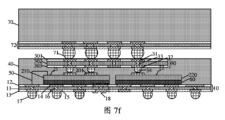
前記第1パッケージ構造は、介在層30及び成形材料40を備え、前記介在層30に第1接続パッド31が設けられ、前記成形材料40は、前記介在層30を包み、前記第1接続パッド31と共面であり、
前記第2パッケージ構造70は、前記介在層30上に設けられ、前記第1接続パッド31に電気接続され、
ここで、前記第1パッケージ構造と前記第2パッケージ構造70との間に隙間がある。
ここで、前記介在層30は、前記第1上部チップ211及び前記第2上部チップ221の上に設けられ、前記第1上部チップ211及び前記第2上部チップ221は、介在層30を介して電気接続される。
2 キャリアテープ
10 基板
11 基板ベース
12 基板上部絶縁誘電体層
13 基板下部絶縁誘電体層
14 基板上部接続パッド
15 基板下部接続パッド
16 基板接続貫通ビア
17 基板接続バンプ
18 仮想チャネル
21 第1チップ積層体
22 第2チップ積層体
210 第1チップ
220 第2チップ
211 第1上部チップ
212 第1下部チップ
221 第2上部チップ
222 第2下部チップ
201 リード線パッド
202 チップ接続パッド
203 チップ接続ハンダボール
30 介在層
31 第1接続パッド
32 第2接続パッド
33 信号チャネル
34 第1ハンダボール
301 介在上部絶縁誘電体層
302 介在基板
303 介在下部絶縁誘電体層
40 成形材料
401 第1充填材
50 リード線
60 接着層
61 第1接着層
62 第2接着層
70 第2パッケージ構造
71 第2ハンダボール
72 第2基板
80 充填層
801 第2充填材
Claims (17)
- 半導体パッケージ構造であって、第1パッケージ構造及び第2パッケージ構造を備え、
前記第1パッケージ構造は、介在層及び成形材料を備え、前記介在層に第1接続パッドが設けられ、前記成形材料は、前記介在層を包み、前記第1接続パッドと共面であり、
前記第2パッケージ構造は、前記介在層の上に設けられ、前記第1接続パッドに電気接続され、
前記第1パッケージ構造と前記第2パッケージ構造との間に隙間があり、
前記第1パッケージ構造は更に、
基板、少なくとも1つの第1チップ積層体及び少なくとも1つの第2チップ積層体を備え、
前記少なくとも1つの第1チップ積層体は、前記基板の上に設けられ、
前記少なくとも1つの第2チップ積層体は、前記基板の上に設けられ、前記第1チップ積層体から間隔をあけて設けられ、
前記介在層は、前記第1チップ積層体及び前記第2チップ積層体上に設けられ、前記第1チップ積層体と前記第2チップ積層体は、前記介在層を介して電気接続され、前記第1チップ積層体の最上部のチップ又は前記第2チップ積層体の最上部のチップは、リード線を介して前記基板に接続される、
半導体パッケージ構造。 - 前記第1チップ積層体は1つの第1チップを備え、前記第2チップ積層体は1つの第2チップを備え、
前記第1チップは、前記介在層を介して前記第2チップに電気接続される、
請求項1に記載の半導体パッケージ構造。 - 前記第1チップ又は前記第2チップは、リード線を介して前記基板に接続される、
請求項2に記載の半導体パッケージ構造。 - 前記第1チップ積層体は、積み重ねられた第1下部チップ及び第1上部チップを備え、前記第2チップ積層体は、積み重ねられた第2下部チップ及び第2上部チップを備え、
前記介在層は、前記第1上部チップ及び前記第2上部チップの上に設けられ、前記第1上部チップ及び前記第2上部チップは、介在層を介して電気接続される、
請求項1に記載の半導体パッケージ構造。 - 前記第1上部チップ又は前記第2上部チップは、リード線を介して前記基板に接続される、
請求項4に記載の半導体パッケージ構造。 - 前記第1下部チップ及び前記第2下部チップはそれぞれ、リード線を介して前記基板に接続される、
請求項5に記載の半導体パッケージ構造。 - 前記第1下部チップは、前記第1上部チップに電気接続され、前記第2下部チップは、前記第2上部チップに電気接続される、
請求項5に記載の半導体パッケージ構造。 - 前記介在層は、
第1表面、第2表面及び信号チャネルを備え、
前記第1表面の上に、前記第1接続パッドが設けられ、
前記第2表面は、前記第1表面に対向して設けられ、前記第2表面の上に第2接続パッドが設けられ、
前記信号チャネルは、前記第1接続パッド及び前記第2接続パッドに接続される、
請求項1~7のいずれか一項に記載の半導体パッケージ構造。 - 前記第1チップ積層体及び前記第2チップ積層体はリード線パッドを備え、前記リード線パッドは、再配線層を介して前記第2接続パッドに接続される、
請求項8に記載の半導体パッケージ構造。 - 前記第1チップ積層体と前記第2チップ積層体とを接続する前記第2接続パッド同士は、再配線層を介して接続される、
請求項8に記載の半導体パッケージ構造。 - 前記第1チップ積層体及び前記第2チップ積層体は、接着層を介して前記基板の上に設けられる、
請求項1に記載の半導体パッケージ構造。 - 前記基板は仮想チャネルを備え、前記接着層は前記仮想チャネルの上に位置し、前記仮想チャネルの熱伝導係数は、前記接着層の熱伝導係数より大きい、
請求項11に記載の半導体パッケージ構造。 - 前記半導体パッケージ構造は更に、充填層を備え、前記充填層は前記隙間を充填する、
請求項1に記載の半導体パッケージ構造。 - 前記充填層の熱伝導係数は、前記成形材料の熱伝導係数より大きい、
請求項13に記載の半導体パッケージ構造。 - 前記充填層の充填材体積は、前記成形材料の充填材体積より小さい、
請求項13に記載の半導体パッケージ構造。 - 前記接着層は、第1接着層及び第2接着層を備え、前記第2接着層は、前記第1接着層の上に位置し、前記第2接着層の弾性率は、前記第1接着層の弾性率より大きい、
請求項11に記載の半導体パッケージ構造。 - 半導体パッケージ構造の製造方法であって、
第1パッケージ構造を提供することであって、前記第1パッケージ構造は、介在層及び成形材料を備え、前記介在層に第1接続パッドが設けられ、前記成形材料は、前記介在層を包み、前記第1接続パッドと共面である、ことと、
第2パッケージ構造を前記介在層の上に設けるように前記第2パッケージ構造を提供することであって、前記第2パッケージ構造は、前記第1接続パッドに電気接続される、ことと、を含み、
前記第1パッケージ構造と前記第2パッケージ構造との間に隙間があり、
前記第1パッケージ構造は更に、
基板、少なくとも1つの第1チップ積層体及び少なくとも1つの第2チップ積層体を備え、
前記少なくとも1つの第1チップ積層体は、前記基板の上に設けられ、
前記少なくとも1つの第2チップ積層体は、前記基板の上に設けられ、前記第1チップ積層体から間隔をあけて設けられ、
前記介在層は、前記第1チップ積層体及び前記第2チップ積層体上に設けられ、前記第1チップ積層体と前記第2チップ積層体は、前記介在層を介して電気接続され、前記第1チップ積層体の最上部のチップ又は前記第2チップ積層体の最上部のチップは、リード線を介して前記基板に接続される、
半導体パッケージ構造の製造方法。
Applications Claiming Priority (3)
| Application Number | Priority Date | Filing Date | Title |
|---|---|---|---|
| CN202210853472.6A CN117410261A (zh) | 2022-07-08 | 2022-07-08 | 半导体封装结构及制备方法 |
| CN202210853472.6 | 2022-07-08 | ||
| PCT/CN2022/110253 WO2024007405A1 (zh) | 2022-07-08 | 2022-08-04 | 半导体封装结构及制备方法 |
Publications (2)
| Publication Number | Publication Date |
|---|---|
| JP2024527645A JP2024527645A (ja) | 2024-07-26 |
| JP7650293B2 true JP7650293B2 (ja) | 2025-03-24 |
Family
ID=89430756
Family Applications (1)
| Application Number | Title | Priority Date | Filing Date |
|---|---|---|---|
| JP2022566266A Active JP7650293B2 (ja) | 2022-07-08 | 2022-08-04 | 半導体パッケージ構造及び製造方法 |
Country Status (4)
| Country | Link |
|---|---|
| US (1) | US12444727B2 (ja) |
| EP (1) | EP4325561A4 (ja) |
| JP (1) | JP7650293B2 (ja) |
| KR (1) | KR102727305B1 (ja) |
Citations (10)
| Publication number | Priority date | Publication date | Assignee | Title |
|---|---|---|---|---|
| JP2005026680A (ja) | 2003-06-30 | 2005-01-27 | Samsung Electronics Co Ltd | 積層型ボールグリッドアレイパッケージ及びその製造方法 |
| JP2006522478A (ja) | 2003-04-04 | 2006-09-28 | チップパック,インク. | プロセッサ及びメモリパッケージアッセンブリを含む半導体マルチパッケージモジュール |
| US20100072593A1 (en) | 2008-09-24 | 2010-03-25 | Samsung Electronics Co., Ltd. | Semiconductor package and method for manufacturing the same |
| US20110127662A1 (en) | 2009-12-02 | 2011-06-02 | Yang Deokkyung | Integrated circuit packaging system with stackable package and method of manufacture thereof |
| JP2011233672A (ja) | 2010-04-27 | 2011-11-17 | Elpida Memory Inc | 半導体装置および半導体装置の製造方法 |
| JP2012156238A (ja) | 2011-01-25 | 2012-08-16 | Elpida Memory Inc | 半導体装置 |
| US20180269187A1 (en) | 2017-03-16 | 2018-09-20 | Intel Corporation | Multi-package integrated circuit assembly with through-mold via |
| US20190206827A1 (en) | 2017-12-29 | 2019-07-04 | Intel Corporation | Semiconductor package with externally accessible wirebonds |
| US20200381406A1 (en) | 2017-09-29 | 2020-12-03 | Intel Corporation | High density die package configuration on system boards |
| US20220199593A1 (en) | 2020-12-22 | 2022-06-23 | Mediatek Inc. | Semiconductor device with dummy thermal features on interposer |
Family Cites Families (66)
| Publication number | Priority date | Publication date | Assignee | Title |
|---|---|---|---|---|
| JPS60160645A (ja) | 1984-02-01 | 1985-08-22 | Hitachi Ltd | 積層半導体集積回路装置 |
| JP3433193B2 (ja) | 2000-10-23 | 2003-08-04 | 松下電器産業株式会社 | 半導体チップおよびその製造方法 |
| US6794273B2 (en) | 2002-05-24 | 2004-09-21 | Fujitsu Limited | Semiconductor device and manufacturing method thereof |
| JP2004172157A (ja) | 2002-11-15 | 2004-06-17 | Shinko Electric Ind Co Ltd | 半導体パッケージおよびパッケージスタック半導体装置 |
| US6861288B2 (en) | 2003-01-23 | 2005-03-01 | St Assembly Test Services, Ltd. | Stacked semiconductor packages and method for the fabrication thereof |
| TWI311353B (en) | 2003-04-18 | 2009-06-21 | Advanced Semiconductor Eng | Stacked chip package structure |
| US7354800B2 (en) | 2005-04-29 | 2008-04-08 | Stats Chippac Ltd. | Method of fabricating a stacked integrated circuit package system |
| CN100417312C (zh) | 2005-09-06 | 2008-09-03 | 威盛电子股份有限公司 | 具有改善散热结构的印刷电路板及电子装置 |
| US8609463B2 (en) | 2007-03-16 | 2013-12-17 | Stats Chippac Ltd. | Integrated circuit package system employing multi-package module techniques |
| CN100483703C (zh) | 2007-05-25 | 2009-04-29 | 日月光半导体制造股份有限公司 | 堆叠式半导体封装结构及其制造方法 |
| US7800211B2 (en) | 2007-06-29 | 2010-09-21 | Stats Chippac, Ltd. | Stackable package by using internal stacking modules |
| US8124451B2 (en) | 2007-09-21 | 2012-02-28 | Stats Chippac Ltd. | Integrated circuit packaging system with interposer |
| KR101413220B1 (ko) | 2007-10-02 | 2014-06-30 | 삼성전자주식회사 | 인터포저를 포함하는 반도체 패키지 및 반도체 패키지의 제조방법 |
| TW200917431A (en) | 2007-10-05 | 2009-04-16 | Advanced Semiconductor Eng | Stacked-type chip package structure and method of fabricating the same |
| KR100961309B1 (ko) | 2008-02-25 | 2010-06-04 | 앰코 테크놀로지 코리아 주식회사 | 반도체 패키지 |
| KR100961308B1 (ko) * | 2008-02-25 | 2010-06-04 | 앰코 테크놀로지 코리아 주식회사 | 반도체 패키지 |
| US7901987B2 (en) | 2008-03-19 | 2011-03-08 | Stats Chippac Ltd. | Package-on-package system with internal stacking module interposer |
| US20090243068A1 (en) | 2008-03-26 | 2009-10-01 | Heap Hoe Kuan | Integrated circuit package system with non-symmetrical support structures |
| TWI395346B (zh) | 2008-05-23 | 2013-05-01 | Xintec Inc | 發光元件的封裝結構 |
| US8102666B2 (en) | 2008-08-19 | 2012-01-24 | Stats Chippac Ltd. | Integrated circuit package system |
| US7859099B2 (en) | 2008-12-11 | 2010-12-28 | Stats Chippac Ltd. | Integrated circuit packaging system having through silicon via with direct interconnects and method of manufacture thereof |
| JP2010212605A (ja) | 2009-03-12 | 2010-09-24 | Toshiba Corp | 半導体装置及びその製造方法 |
| US7923290B2 (en) * | 2009-03-27 | 2011-04-12 | Stats Chippac Ltd. | Integrated circuit packaging system having dual sided connection and method of manufacture thereof |
| KR20100112446A (ko) | 2009-04-09 | 2010-10-19 | 삼성전자주식회사 | 적층형 반도체 패키지 및 그 제조 방법 |
| JP2010278318A (ja) | 2009-05-29 | 2010-12-09 | Renesas Electronics Corp | 半導体装置 |
| US7927917B2 (en) | 2009-06-19 | 2011-04-19 | Stats Chippac Ltd. | Integrated circuit packaging system with inward and outward interconnects and method of manufacture thereof |
| TWI419283B (zh) | 2010-02-10 | 2013-12-11 | 日月光半導體製造股份有限公司 | 封裝結構 |
| US8466544B2 (en) * | 2011-02-25 | 2013-06-18 | Stats Chippac, Ltd. | Semiconductor device and method of forming interposer and opposing build-up interconnect structure with connecting conductive TMV for electrical interconnect of Fo-WLCSP |
| US20120228751A1 (en) | 2011-03-07 | 2012-09-13 | Samsung Electronics Co., Ltd. | Semiconductor package and method of manufacturing the same |
| US8692365B2 (en) | 2011-06-17 | 2014-04-08 | Stats Chippac Ltd. | Integrated circuit packaging system with thermal dispersal structures and method of manufacture thereof |
| US8962393B2 (en) | 2011-09-23 | 2015-02-24 | Stats Chippac Ltd. | Integrated circuit packaging system with heat shield and method of manufacture thereof |
| US8614105B2 (en) | 2011-09-28 | 2013-12-24 | Taiwan Semiconductor Manufacturing Company, Ltd. | Production flow and reusable testing method |
| US9418947B2 (en) | 2012-02-27 | 2016-08-16 | Taiwan Semiconductor Manufacturing Company, Ltd. | Mechanisms for forming connectors with a molding compound for package on package |
| US9842798B2 (en) | 2012-03-23 | 2017-12-12 | STATS ChipPAC Pte. Ltd. | Semiconductor device and method of forming a PoP device with embedded vertical interconnect units |
| US8975726B2 (en) | 2012-10-11 | 2015-03-10 | Taiwan Semiconductor Manufacturing Company, Ltd. | POP structures and methods of forming the same |
| CN103219296B (zh) | 2013-03-29 | 2016-04-13 | 三星半导体(中国)研究开发有限公司 | 用于半导体封装的多功能膜及其制造方法 |
| KR102108325B1 (ko) | 2013-10-14 | 2020-05-08 | 삼성전자주식회사 | 반도체 패키지 |
| KR102245770B1 (ko) | 2013-10-29 | 2021-04-28 | 삼성전자주식회사 | 반도체 패키지 장치 |
| US9196586B2 (en) | 2014-02-13 | 2015-11-24 | Taiwan Semiconductor Manufacturing Company, Ltd. | Semiconductor package including an embedded surface mount device and method of forming the same |
| CN204102862U (zh) | 2014-08-01 | 2015-01-14 | 深圳市兴森快捷电路科技股份有限公司 | 一种基于腔体技术多芯片叠加封装装置 |
| CN105161435A (zh) | 2015-07-06 | 2015-12-16 | 华进半导体封装先导技术研发中心有限公司 | 控制球高且避免掉球的PoP堆叠封装工艺 |
| US9595509B1 (en) | 2015-09-08 | 2017-03-14 | Nxp Usa, Inc. | Stacked microelectronic package assemblies and methods for the fabrication thereof |
| KR101681031B1 (ko) | 2015-11-17 | 2016-12-01 | 주식회사 네패스 | 반도체 패키지 및 그 제조방법 |
| US9904776B2 (en) | 2016-02-10 | 2018-02-27 | Taiwan Semiconductor Manufacturing Company, Ltd. | Fingerprint sensor pixel array and methods of forming same |
| EP3399548A1 (en) | 2016-06-15 | 2018-11-07 | MediaTek Inc. | Semiconductor package incorporating redistribution layer interposer |
| CN107579061B (zh) | 2016-07-04 | 2020-01-07 | 晟碟信息科技(上海)有限公司 | 包含互连的叠加封装体的半导体装置 |
| CN110062956B (zh) | 2016-12-30 | 2023-10-10 | 英特尔公司 | 用于高频通信的利用三维堆叠超薄封装模块设计的微电子器件 |
| KR20190004964A (ko) | 2017-07-05 | 2019-01-15 | 삼성전자주식회사 | 반도체 패키지 |
| DE102018202364B4 (de) | 2018-02-15 | 2022-10-13 | Fraunhofer-Gesellschaft zur Förderung der angewandten Forschung e.V. | Moduleinheit mit integrierten Antennen und Verfahren zum Herstellen derselben |
| DE102018125280B4 (de) | 2018-03-23 | 2022-04-14 | Taiwan Semiconductor Manufacturing Company, Ltd. | Halbleiter-Package und Verfahren |
| US11069671B2 (en) | 2018-03-23 | 2021-07-20 | Taiwan Semiconductor Manufacturing Company, Ltd. | Semiconductor package and method |
| KR102519571B1 (ko) | 2018-06-11 | 2023-04-10 | 삼성전자주식회사 | 반도체 패키지 |
| KR20200007509A (ko) | 2018-07-13 | 2020-01-22 | 삼성전자주식회사 | 반도체 패키지 |
| US11211334B2 (en) | 2018-11-18 | 2021-12-28 | iCometrue Company Ltd. | Logic drive based on chip scale package comprising standardized commodity programmable logic IC chip and memory IC chip |
| KR102589684B1 (ko) | 2018-12-14 | 2023-10-17 | 삼성전자주식회사 | 반도체 패키지 |
| KR102677777B1 (ko) | 2019-04-01 | 2024-06-25 | 삼성전자주식회사 | 반도체 패키지 |
| KR102677593B1 (ko) | 2019-05-28 | 2024-06-24 | 에스케이하이닉스 주식회사 | 인터커넥트 구조를 포함한 스택 패키지 |
| US11562983B2 (en) | 2019-06-28 | 2023-01-24 | Taiwan Semiconductor Manufacturing Company, Ltd. | Package having multiple chips integrated therein and manufacturing method thereof |
| KR102728523B1 (ko) | 2019-07-31 | 2024-11-13 | 삼성전자주식회사 | 반도체 패키지 |
| KR102717843B1 (ko) | 2019-08-02 | 2024-10-16 | 삼성전자주식회사 | 반도체 패키지 및 그의 제조 방법 |
| TW202109800A (zh) | 2019-08-15 | 2021-03-01 | 力成科技股份有限公司 | 具有微細間距矽穿孔封裝的扇出型封裝晶片結構以及扇出型封裝單元 |
| CN110797325B (zh) | 2019-12-12 | 2025-07-29 | 江阴长电先进封装有限公司 | 一种具有电磁屏蔽功能的封装结构及其封装方法 |
| WO2021146860A1 (zh) | 2020-01-20 | 2021-07-29 | 深圳市汇顶科技股份有限公司 | 堆叠式的芯片、制造方法、图像传感器和电子设备 |
| US11521905B2 (en) * | 2020-10-21 | 2022-12-06 | Taiwan Semiconductor Manufacturing Company, Ltd. | Package structure and method of manufacturing the same |
| TWM627599U (zh) | 2021-11-16 | 2022-06-01 | 華碩電腦股份有限公司 | 封裝結構 |
| JP2024160645A (ja) | 2023-05-01 | 2024-11-14 | キヤノン株式会社 | 画像形成装置 |
-
2022
- 2022-08-04 JP JP2022566266A patent/JP7650293B2/ja active Active
- 2022-08-04 KR KR1020227041847A patent/KR102727305B1/ko active Active
- 2022-08-04 EP EP22793375.1A patent/EP4325561A4/en active Pending
-
2023
- 2023-01-10 US US18/152,188 patent/US12444727B2/en active Active
Patent Citations (10)
| Publication number | Priority date | Publication date | Assignee | Title |
|---|---|---|---|---|
| JP2006522478A (ja) | 2003-04-04 | 2006-09-28 | チップパック,インク. | プロセッサ及びメモリパッケージアッセンブリを含む半導体マルチパッケージモジュール |
| JP2005026680A (ja) | 2003-06-30 | 2005-01-27 | Samsung Electronics Co Ltd | 積層型ボールグリッドアレイパッケージ及びその製造方法 |
| US20100072593A1 (en) | 2008-09-24 | 2010-03-25 | Samsung Electronics Co., Ltd. | Semiconductor package and method for manufacturing the same |
| US20110127662A1 (en) | 2009-12-02 | 2011-06-02 | Yang Deokkyung | Integrated circuit packaging system with stackable package and method of manufacture thereof |
| JP2011233672A (ja) | 2010-04-27 | 2011-11-17 | Elpida Memory Inc | 半導体装置および半導体装置の製造方法 |
| JP2012156238A (ja) | 2011-01-25 | 2012-08-16 | Elpida Memory Inc | 半導体装置 |
| US20180269187A1 (en) | 2017-03-16 | 2018-09-20 | Intel Corporation | Multi-package integrated circuit assembly with through-mold via |
| US20200381406A1 (en) | 2017-09-29 | 2020-12-03 | Intel Corporation | High density die package configuration on system boards |
| US20190206827A1 (en) | 2017-12-29 | 2019-07-04 | Intel Corporation | Semiconductor package with externally accessible wirebonds |
| US20220199593A1 (en) | 2020-12-22 | 2022-06-23 | Mediatek Inc. | Semiconductor device with dummy thermal features on interposer |
Also Published As
| Publication number | Publication date |
|---|---|
| US12444727B2 (en) | 2025-10-14 |
| KR102727305B1 (ko) | 2024-11-11 |
| US20240014196A1 (en) | 2024-01-11 |
| JP2024527645A (ja) | 2024-07-26 |
| EP4325561A4 (en) | 2024-12-11 |
| KR20240007878A (ko) | 2024-01-17 |
| EP4325561A1 (en) | 2024-02-21 |
Similar Documents
| Publication | Publication Date | Title |
|---|---|---|
| CN103700633B (zh) | 半导体封装件 | |
| TWI753587B (zh) | 封裝結構及其形成方法 | |
| US7361986B2 (en) | Heat stud for stacked chip package | |
| KR101623880B1 (ko) | 반도체 패키지 | |
| CN111799234A (zh) | 包括热传导网络结构的半导体封装件 | |
| US20240038728A1 (en) | Semiconductor package | |
| JP7650293B2 (ja) | 半導体パッケージ構造及び製造方法 | |
| TWM627599U (zh) | 封裝結構 | |
| KR102849161B1 (ko) | 반도체 패키지 및 반도체 패키지의 제조 방법 | |
| US20240014190A1 (en) | Semiconductor package structure and method for fabracating the same | |
| US20110304038A1 (en) | Semiconductor chip designed to dissipate heat effectively, semiconductor package including the same, and stack package using the same | |
| KR102601150B1 (ko) | 반도체 패키지 | |
| TWI835354B (zh) | 半導體封裝結構及製備方法 | |
| TWI790054B (zh) | 天線整合式封裝結構 | |
| CN214898441U (zh) | 一种封装组件及电子设备 | |
| TWI835286B (zh) | 半導體封裝結構及製備方法 | |
| WO2024082348A1 (zh) | 一种半导体封装结构及制备方法 | |
| JP7766043B2 (ja) | 半導体パッケージアセンブリ及び製造方法 | |
| JP7676440B2 (ja) | 半導体パッケージ構造及び製造方法 | |
| US20230422521A1 (en) | Stack-type semiconductor package | |
| CN117954417A (zh) | 一种半导体封装结构及制备方法 | |
| US12482721B2 (en) | Semiconductor package including heat dissipation structure | |
| US20250062303A1 (en) | Semiconductor packages | |
| JP2024530373A (ja) | 半導体パッケージアセンブリ及び製造方法 | |
| JP2025160423A (ja) | 半導体パッケージ |
Legal Events
| Date | Code | Title | Description |
|---|---|---|---|
| A621 | Written request for application examination |
Free format text: JAPANESE INTERMEDIATE CODE: A621 Effective date: 20221028 |
|
| A131 | Notification of reasons for refusal |
Free format text: JAPANESE INTERMEDIATE CODE: A131 Effective date: 20241008 |
|
| A521 | Request for written amendment filed |
Free format text: JAPANESE INTERMEDIATE CODE: A523 Effective date: 20241120 |
|
| TRDD | Decision of grant or rejection written | ||
| A01 | Written decision to grant a patent or to grant a registration (utility model) |
Free format text: JAPANESE INTERMEDIATE CODE: A01 Effective date: 20250305 |
|
| A61 | First payment of annual fees (during grant procedure) |
Free format text: JAPANESE INTERMEDIATE CODE: A61 Effective date: 20250311 |
|
| R150 | Certificate of patent or registration of utility model |
Ref document number: 7650293 Country of ref document: JP Free format text: JAPANESE INTERMEDIATE CODE: R150 |