JP7584585B2 - Semiconductor Device - Google Patents
Semiconductor Device Download PDFInfo
- Publication number
- JP7584585B2 JP7584585B2 JP2023116445A JP2023116445A JP7584585B2 JP 7584585 B2 JP7584585 B2 JP 7584585B2 JP 2023116445 A JP2023116445 A JP 2023116445A JP 2023116445 A JP2023116445 A JP 2023116445A JP 7584585 B2 JP7584585 B2 JP 7584585B2
- Authority
- JP
- Japan
- Prior art keywords
- layer
- insulating layer
- electrode layer
- oxide semiconductor
- transistor
- Prior art date
- Legal status (The legal status is an assumption and is not a legal conclusion. Google has not performed a legal analysis and makes no representation as to the accuracy of the status listed.)
- Active
Links
Images


Classifications
-
- H—ELECTRICITY
- H04—ELECTRIC COMMUNICATION TECHNIQUE
- H04B—TRANSMISSION
- H04B1/00—Details of transmission systems, not covered by a single one of groups H04B3/00 - H04B13/00; Details of transmission systems not characterised by the medium used for transmission
- H04B1/38—Transceivers, i.e. devices in which transmitter and receiver form a structural unit and in which at least one part is used for functions of transmitting and receiving
- H04B1/40—Circuits
-
- H—ELECTRICITY
- H10—SEMICONDUCTOR DEVICES; ELECTRIC SOLID-STATE DEVICES NOT OTHERWISE PROVIDED FOR
- H10D—INORGANIC ELECTRIC SEMICONDUCTOR DEVICES
- H10D30/00—Field-effect transistors [FET]
- H10D30/60—Insulated-gate field-effect transistors [IGFET]
- H10D30/67—Thin-film transistors [TFT]
- H10D30/6757—Thin-film transistors [TFT] characterised by the structure of the channel, e.g. transverse or longitudinal shape or doping profile
-
- G—PHYSICS
- G06—COMPUTING OR CALCULATING; COUNTING
- G06K—GRAPHICAL DATA READING; PRESENTATION OF DATA; RECORD CARRIERS; HANDLING RECORD CARRIERS
- G06K19/00—Record carriers for use with machines and with at least a part designed to carry digital markings
- G06K19/06—Record carriers for use with machines and with at least a part designed to carry digital markings characterised by the kind of the digital marking, e.g. shape, nature, code
- G06K19/067—Record carriers with conductive marks, printed circuits or semiconductor circuit elements, e.g. credit or identity cards also with resonating or responding marks without active components
- G06K19/07—Record carriers with conductive marks, printed circuits or semiconductor circuit elements, e.g. credit or identity cards also with resonating or responding marks without active components with integrated circuit chips
- G06K19/077—Constructional details, e.g. mounting of circuits in the carrier
- G06K19/07749—Constructional details, e.g. mounting of circuits in the carrier the record carrier being capable of non-contact communication, e.g. constructional details of the antenna of a non-contact smart card
- G06K19/07773—Antenna details
-
- H—ELECTRICITY
- H10—SEMICONDUCTOR DEVICES; ELECTRIC SOLID-STATE DEVICES NOT OTHERWISE PROVIDED FOR
- H10D—INORGANIC ELECTRIC SEMICONDUCTOR DEVICES
- H10D30/00—Field-effect transistors [FET]
- H10D30/60—Insulated-gate field-effect transistors [IGFET]
- H10D30/67—Thin-film transistors [TFT]
- H10D30/674—Thin-film transistors [TFT] characterised by the active materials
- H10D30/6755—Oxide semiconductors, e.g. zinc oxide, copper aluminium oxide or cadmium stannate
-
- H—ELECTRICITY
- H10—SEMICONDUCTOR DEVICES; ELECTRIC SOLID-STATE DEVICES NOT OTHERWISE PROVIDED FOR
- H10D—INORGANIC ELECTRIC SEMICONDUCTOR DEVICES
- H10D62/00—Semiconductor bodies, or regions thereof, of devices having potential barriers
- H10D62/10—Shapes, relative sizes or dispositions of the regions of the semiconductor bodies; Shapes of the semiconductor bodies
- H10D62/17—Semiconductor regions connected to electrodes not carrying current to be rectified, amplified or switched, e.g. channel regions
- H10D62/213—Channel regions of field-effect devices
- H10D62/221—Channel regions of field-effect devices of FETs
- H10D62/235—Channel regions of field-effect devices of FETs of IGFETs
-
- H—ELECTRICITY
- H10—SEMICONDUCTOR DEVICES; ELECTRIC SOLID-STATE DEVICES NOT OTHERWISE PROVIDED FOR
- H10D—INORGANIC ELECTRIC SEMICONDUCTOR DEVICES
- H10D86/00—Integrated devices formed in or on insulating or conducting substrates, e.g. formed in silicon-on-insulator [SOI] substrates or on stainless steel or glass substrates
- H10D86/40—Integrated devices formed in or on insulating or conducting substrates, e.g. formed in silicon-on-insulator [SOI] substrates or on stainless steel or glass substrates characterised by multiple TFTs
- H10D86/421—Integrated devices formed in or on insulating or conducting substrates, e.g. formed in silicon-on-insulator [SOI] substrates or on stainless steel or glass substrates characterised by multiple TFTs having a particular composition, shape or crystalline structure of the active layer
- H10D86/423—Integrated devices formed in or on insulating or conducting substrates, e.g. formed in silicon-on-insulator [SOI] substrates or on stainless steel or glass substrates characterised by multiple TFTs having a particular composition, shape or crystalline structure of the active layer comprising semiconductor materials not belonging to the Group IV, e.g. InGaZnO
-
- H—ELECTRICITY
- H10—SEMICONDUCTOR DEVICES; ELECTRIC SOLID-STATE DEVICES NOT OTHERWISE PROVIDED FOR
- H10D—INORGANIC ELECTRIC SEMICONDUCTOR DEVICES
- H10D86/00—Integrated devices formed in or on insulating or conducting substrates, e.g. formed in silicon-on-insulator [SOI] substrates or on stainless steel or glass substrates
- H10D86/40—Integrated devices formed in or on insulating or conducting substrates, e.g. formed in silicon-on-insulator [SOI] substrates or on stainless steel or glass substrates characterised by multiple TFTs
- H10D86/60—Integrated devices formed in or on insulating or conducting substrates, e.g. formed in silicon-on-insulator [SOI] substrates or on stainless steel or glass substrates characterised by multiple TFTs wherein the TFTs are in active matrices
-
- H—ELECTRICITY
- H10—SEMICONDUCTOR DEVICES; ELECTRIC SOLID-STATE DEVICES NOT OTHERWISE PROVIDED FOR
- H10D—INORGANIC ELECTRIC SEMICONDUCTOR DEVICES
- H10D88/00—Three-dimensional [3D] integrated devices
-
- H—ELECTRICITY
- H10—SEMICONDUCTOR DEVICES; ELECTRIC SOLID-STATE DEVICES NOT OTHERWISE PROVIDED FOR
- H10W—GENERIC PACKAGES, INTERCONNECTIONS, CONNECTORS OR OTHER CONSTRUCTIONAL DETAILS OF DEVICES COVERED BY CLASS H10
- H10W44/00—Electrical arrangements for controlling or matching impedance
- H10W44/20—Electrical arrangements for controlling or matching impedance at high-frequency [HF] or radio frequency [RF]
- H10W44/241—Electrical arrangements for controlling or matching impedance at high-frequency [HF] or radio frequency [RF] for passive devices or passive elements
- H10W44/248—Electrical arrangements for controlling or matching impedance at high-frequency [HF] or radio frequency [RF] for passive devices or passive elements for antennas
-
- Y—GENERAL TAGGING OF NEW TECHNOLOGICAL DEVELOPMENTS; GENERAL TAGGING OF CROSS-SECTIONAL TECHNOLOGIES SPANNING OVER SEVERAL SECTIONS OF THE IPC; TECHNICAL SUBJECTS COVERED BY FORMER USPC CROSS-REFERENCE ART COLLECTIONS [XRACs] AND DIGESTS
- Y02—TECHNOLOGIES OR APPLICATIONS FOR MITIGATION OR ADAPTATION AGAINST CLIMATE CHANGE
- Y02D—CLIMATE CHANGE MITIGATION TECHNOLOGIES IN INFORMATION AND COMMUNICATION TECHNOLOGIES [ICT], I.E. INFORMATION AND COMMUNICATION TECHNOLOGIES AIMING AT THE REDUCTION OF THEIR OWN ENERGY USE
- Y02D30/00—Reducing energy consumption in communication networks
- Y02D30/70—Reducing energy consumption in communication networks in wireless communication networks
-
- Y—GENERAL TAGGING OF NEW TECHNOLOGICAL DEVELOPMENTS; GENERAL TAGGING OF CROSS-SECTIONAL TECHNOLOGIES SPANNING OVER SEVERAL SECTIONS OF THE IPC; TECHNICAL SUBJECTS COVERED BY FORMER USPC CROSS-REFERENCE ART COLLECTIONS [XRACs] AND DIGESTS
- Y02—TECHNOLOGIES OR APPLICATIONS FOR MITIGATION OR ADAPTATION AGAINST CLIMATE CHANGE
- Y02E—REDUCTION OF GREENHOUSE GAS [GHG] EMISSIONS, RELATED TO ENERGY GENERATION, TRANSMISSION OR DISTRIBUTION
- Y02E60/00—Enabling technologies; Technologies with a potential or indirect contribution to GHG emissions mitigation
- Y02E60/10—Energy storage using batteries
Landscapes
- Engineering & Computer Science (AREA)
- Computer Networks & Wireless Communication (AREA)
- Computer Hardware Design (AREA)
- Microelectronics & Electronic Packaging (AREA)
- Physics & Mathematics (AREA)
- General Physics & Mathematics (AREA)
- Theoretical Computer Science (AREA)
- Signal Processing (AREA)
- Thin Film Transistor (AREA)
- Metal-Oxide And Bipolar Metal-Oxide Semiconductor Integrated Circuits (AREA)
- Dram (AREA)
Description
本発明は、半導体装置に関する。特に無線通信機能を有する半導体装置に関する。 The present invention relates to a semiconductor device. In particular, the present invention relates to a semiconductor device having a wireless communication function.
なお、本明細書において、半導体装置とは、半導体特性を利用することで機能しうる装
置全般を指し、電気光学装置、半導体回路及び電子機器は全て半導体装置である。
In this specification, the term "semiconductor device" refers to any device that can function by utilizing semiconductor characteristics, and electro-optical devices, semiconductor circuits, and electronic devices are all classified as semiconductor devices.
無線でのデータの送受信が可能な無線通信機能を有する半導体装置は、様々な分野にお
いて実用化が進められている。このような半導体装置は、新しい形態の通信情報端末とし
てさらなる市場の拡大が見込まれている。実用化されている無線通信機能を有する半導体
装置は、アンテナと、半導体素子を用いて形成された集積回路とが同一基板上に形成され
ている。また、無線通信機能を有する半導体装置は、無線タグ、RF(Radio Fr
equency)タグ、RFID(Radio Frequency Identifi
cation)タグ、IC(Integrated Circuit)タグ、またはID
(Identification)タグとも呼ばれる。
Semiconductor devices having a wireless communication function capable of wirelessly transmitting and receiving data are being put to practical use in various fields. Such semiconductor devices are expected to further expand the market as a new type of communication information terminal. Semiconductor devices having a wireless communication function that are in practical use have an antenna and an integrated circuit formed using semiconductor elements formed on the same substrate. Semiconductor devices having a wireless communication function include wireless tags, RF (Radio Frequency)
RFID (Radio Frequency Identification) tags
cation tag, IC (Integrated Circuit) tag, or ID
It is also called an Identification tag.
当該半導体装置は、アクティブ型と、パッシブ型の2種に大別される。前者は、半導体
装置内に電池を有し、該電池を電力供給源として動作する半導体装置であり、後者は、半
導体装置内に電池などの電力供給源が存在せず、外部の質問器(リーダ、リーダライタ、
R/Wともいう)から入力される信号を電力供給源として動作する半導体装置である。
The semiconductor device is roughly divided into two types, an active type and a passive type. The former is a semiconductor device that has a battery in the semiconductor device and operates using the battery as a power supply source, while the latter is a semiconductor device that does not have a power supply source such as a battery in the semiconductor device and operates using an external interrogator (reader, reader/writer,
The semiconductor device operates using a signal input from a power supply source.
アクティブ型無線タグは、電力供給源を内蔵しているため、パッシブ型無線タグと比較
し質問器との通信距離を長くすることができる。ただし、アクティブ型無線タグは、応答
する質問器の有無にかかわらず常時又は定期的に動作(信号の生成)を行うため、消費電
力が大きくなる。
Since active wireless tags have a built-in power supply source, they can communicate with an interrogator over a longer distance than passive wireless tags. However, active wireless tags consume more power because they operate (generate signals) constantly or periodically, regardless of whether there is an interrogator responding.
アクティブ型無線タグの消費電力を低減する技術が特許文献1に開示されている。特許
文献1で開示されるアクティブ型無線タグ(アクティブ無線タグ)は、従来のアクティブ
型無線タグの構成に加えて、外部からの信号を受信する第2のアンテナと、当該信号を用
いて発電する発電器と、該発電器の出力電圧が入力される電圧検知回路とを有し、該電圧
検知回路によって間欠動作が制御される。これにより、消費電力を低減することができる
。
A technology for reducing the power consumption of an active wireless tag is disclosed in
しかしながら、間欠動作を行う半導体装置で消費される電力は、動作時における消費電
力のみならず待機時における消費電力(以下、待機電力ともいう)も含まれる。なお、こ
こでは、待機電力とは、電池が電気的に接続された素子又は回路を介した微量な放電に起
因する消費電力を指す。特に、特許文献1で開示される間欠動作を制御することが可能な
半導体装置においては、消費電力に占める待機電力の割合が高くなる。そのため、当該半
導体装置において消費電力を低減するには、待機電力を低減することが重要となる。
However, the power consumed by a semiconductor device that performs intermittent operation includes not only the power consumed during operation but also the power consumed during standby (hereinafter also referred to as standby power). Note that here, standby power refers to the power consumed due to a small amount of discharge via an element or circuit to which a battery is electrically connected. In particular, in the semiconductor device capable of controlling intermittent operation disclosed in
そこで、本発明の一態様は、半導体装置の待機電力を低減することを課題の一とする。 Therefore, one aspect of the present invention is to reduce the standby power of a semiconductor device.
また、本発明の一態様は、半導体装置を長寿命化することを課題の一とする。 Another object of one embodiment of the present invention is to extend the life of a semiconductor device.
上記課題は、電力供給源となる電池と、特定の回路とがチャネル形成領域が酸化物半導
体によって構成されるトランジスタを介して電気的に接続されることによって解決するこ
とができる。なお、当該酸化物半導体は、電子供与体(ドナー)となる水素を除去するこ
とで、真性又は実質的に真性な半導体である。
The above-mentioned problem can be solved by electrically connecting a battery serving as a power supply source and a specific circuit through a transistor having a channel formation region made of an oxide semiconductor. Note that the oxide semiconductor becomes an intrinsic or substantially intrinsic semiconductor by removing hydrogen serving as an electron donor.
具体的には、当該酸化物半導体に含まれる水素が5×10¹⁹(atoms/cm3)
以下、好ましくは5×10¹⁸(atoms/cm3)以下、より好ましくは5×101
7(atoms/cm3)以下である。このように水素濃度を低減することによって、キ
ャリア密度を1×1014cm-3未満、好ましくは1×1012cm-3未満、さらに
好ましくは測定限界以下の1×1011cm-3未満とすることが可能になる。
Specifically, the hydrogen concentration in the oxide semiconductor is 5×10 19 (atoms/cm 3 )
or less, preferably 5×10 18 (atoms/cm 3 ) or less, more preferably 5×10 1
7 (atoms/cm 3 ) or less. By reducing the hydrogen concentration in this manner, it is possible to make the carrier density less than 1×10 14 cm -3 , preferably less than 1×10 12 cm -3 , and more preferably less than 1×10 11 cm -3 , which is the measurement limit or less.
このように高純度化された酸化物半導体をトランジスタのチャネル形成領域に用いるこ
とで、チャネル幅が10mmの場合でさえも、当該トランジスタのオフ状態におけるドレ
イン電流は1×10-13[A]以下となるように作用する。すなわち、高純度化された
酸化物半導体をトランジスタのチャネル形成領域に適用することによって、リーク電流を
大幅に低減することができる。
By using such a highly purified oxide semiconductor for a channel formation region of a transistor, the drain current of the transistor in an off state can be made 1×10 A or less even when the channel width is 10 mm. In other words, by using a highly purified oxide semiconductor for the channel formation region of a transistor, leakage current can be significantly reduced.
すなわち、本発明の一態様は、アンテナと、電池と、アンテナから入力される信号を復
調する復調回路と、復調回路から入力される信号及び電池から供給される電源電圧を用い
て動作する信号処理部と、復調回路から入力される信号によって制御されるパワー制御回
路と、を有し、信号処理部は、パワー制御回路から入力される信号によってスイッチング
が制御されるトランジスタと、トランジスタを介して電池の陽極又は陰極に電気的に接続
された機能回路と、を有し、トランジスタのチャネル形成領域は、水素濃度が5×101
9(atoms/cm3)以下の酸化物半導体によって構成される半導体装置である。
That is, one embodiment of the present invention includes an antenna, a battery, a demodulation circuit that demodulates a signal input from the antenna, a signal processing unit that operates using a signal input from the demodulation circuit and a power supply voltage supplied from the battery, and a power control circuit controlled by the signal input from the demodulation circuit, the signal processing unit includes a transistor whose switching is controlled by a signal input from the power control circuit, and a functional circuit electrically connected to an anode or a cathode of the battery through the transistor, and a channel formation region of the transistor has a hydrogen concentration of 5× 10
The semiconductor device is formed using an oxide semiconductor having a dopant concentration of 0.9 (atoms/cm 3 ) or less.
また、上記構成に含まれる復調回路はタイマーに置換することが可能である。つまり、
アンテナと、電池と、定期的に信号を出力するタイマーと、タイマーから入力される信号
及び電池から供給される電源電圧を用いて動作する信号処理部と、タイマーから入力され
る信号によって制御されるパワー制御回路と、を有し、信号処理部は、パワー制御回路か
ら入力される信号によってスイッチングが制御されるトランジスタと、トランジスタを介
して電池の陽極又は陰極に電気的に接続された機能回路と、を有し、トランジスタのチャ
ネル形成領域は、水素濃度が5×10¹⁹(atoms/cm3)以下の酸化物半導体に
よって構成される半導体装置も本発明の一態様である。
Also, the demodulation circuit included in the above configuration can be replaced with a timer.
Another embodiment of the present invention is a semiconductor device including an antenna, a battery, a timer that periodically outputs a signal, a signal processing unit that operates using a signal input from the timer and a power supply voltage supplied from the battery, and a power control circuit controlled by the signal input from the timer, where the signal processing unit includes a transistor whose switching is controlled by the signal input from the power control circuit, and a functional circuit electrically connected to an anode or a cathode of the battery via the transistor, and a channel formation region of the transistor is formed using an oxide semiconductor having a hydrogen concentration of 5×10 19 (atoms/cm 3 ) or less.
また、上記構成における電池が二次電池であり、且つ上記構成に加えて、アンテナから
入力される信号を整流する整流回路と、整流回路から入力される信号を用いて二次電池を
充電する充電回路と、二次電池を用いて電源電圧を生成する安定化電源回路と、を有する
半導体装置も本発明の一態様である。
Another embodiment of the present invention is a semiconductor device in which the battery in the above structure is a secondary battery and, in addition to the above structure, the semiconductor device has a rectifier circuit that rectifies a signal input from an antenna, a charging circuit that charges the secondary battery using the signal input from the rectifier circuit, and a stabilized power supply circuit that generates a power supply voltage using the secondary battery.
なお、上記の機能回路としては、例えば論理ゲートなどが挙げられる。当該論理ゲート
は、相補型金属酸化膜半導体(CMOS)によって構成することが可能であるし、N型ト
ランジスタ(NMOS)のみによって構成することも可能である。
The functional circuit may be, for example, a logic gate. The logic gate may be configured using complementary metal-oxide semiconductor (CMOS) or may be configured using only N-type transistors (NMOS).
本発明の一態様の半導体装置は、機能回路と、電池と、機能回路と電池の電気的な接続
を制御するトランジスタとを有する。該トランジスタのチャネル形成領域は、水素濃度が
低減された酸化物半導体によって構成される。具体的には、当該酸化物半導体の水素濃度
は、5×10¹⁹(atoms/cm3)以下である。そのため、待機状態において当該
トランジスタをオフすることにより、当該トランジスタを介した放電を抑制することがで
きる。その結果、当該半導体装置の待機電力を低減することができる。また、待機状態に
おける電池の放電を低減することで、半導体装置を長寿命化することができる。
A semiconductor device according to one embodiment of the present invention includes a functional circuit, a battery, and a transistor that controls electrical connection between the functional circuit and the battery. A channel formation region of the transistor is formed using an oxide semiconductor in which hydrogen concentration is reduced. Specifically, the hydrogen concentration of the oxide semiconductor is 5×10 19 (atoms/cm 3 ) or less. Therefore, by turning off the transistor in a standby state, discharge through the transistor can be suppressed. As a result, standby power of the semiconductor device can be reduced. Furthermore, by reducing discharge of the battery in a standby state, the life of the semiconductor device can be extended.
以下では、本発明の実施の形態について図面を用いて詳細に説明する。ただし、本発明
は以下の説明に限定されず、本発明の趣旨およびその範囲から逸脱することなくその形態
および詳細を様々に変更し得ることは、当業者であれば容易に理解される。したがって、
本発明は以下に示す実施の形態の記載内容に限定して解釈されるものではない。
Hereinafter, the embodiments of the present invention will be described in detail with reference to the drawings. However, the present invention is not limited to the following description, and it will be easily understood by those skilled in the art that the form and details of the present invention can be modified in various ways without departing from the spirit and scope of the present invention. Therefore,
The present invention should not be construed as being limited to the description of the following embodiments.
なお、トランジスタのソース端子及びドレイン端子は、トランジスタの構造や動作条件
等によって替わるため、いずれがソース端子又はドレイン端子であるかを特定することが
困難である。そこで、本書類においては、ソース端子及びドレイン端子の一方を第1端子
、ソース端子及びドレイン端子の他方を第2端子と表記し、区別することとする。
In addition, since the source terminal and the drain terminal of a transistor change depending on the structure, operating conditions, etc. of the transistor, it is difficult to specify which is the source terminal and which is the drain terminal. Therefore, in this document, one of the source terminal and the drain terminal is referred to as a first terminal, and the other of the source terminal and the drain terminal is referred to as a second terminal to distinguish them.
また、各実施の形態の図面等において示す各構成の、大きさ、層の厚さ、又は領域は、
明瞭化のために誇張されて表記している場合がある。よって、必ずしもそのスケールに限
定されない。また、本明細書にて用いる「第1」、「第2」、「第3」などの序数は、構
成要素の混同を避けるために付したものであり、数的に限定するものではないことを付記
する。
In addition, the size, layer thickness, or area of each component shown in the drawings of each embodiment may differ from the actual size, layer thickness, or area shown in the drawings of each embodiment.
In some cases, the figures are exaggerated for clarity. Therefore, the figures are not necessarily limited to the scale. In addition, ordinal numbers such as "first,""second," and "third" used in this specification are given to avoid confusion of components, and are not intended to limit the numbers.
(実施の形態1)
本実施の形態では、半導体装置の一例について説明する。具体的には、電池を電力供給
源とした無線通信機能を有する半導体装置の一例について図1を参照して説明する。
(Embodiment 1)
In this embodiment, an example of a semiconductor device will be described. Specifically, an example of a semiconductor device having a wireless communication function using a battery as a power supply source will be described with reference to FIG.
図1に示す半導体装置は、無線信号の送受信が可能なアンテナ10と、電源電圧(VD
D)の供給源となる電池11と、アンテナ10から入力される信号を復調する復調回路1
2と、復調回路12から入力される信号及び電池11から供給される電源電圧(VDD)
を用いて動作する信号処理部13と、復調回路12から入力される信号及び信号処理部1
3から入力される信号によって制御されるパワー制御回路14とを有する。なお、本実施
の形態において、動作とは、信号処理部13又は信号処理部13の一部において行われる
信号の生成を指すこととする。
The semiconductor device shown in FIG. 1 includes an
D) a
2, a signal input from the
A
and a
さらに、信号処理部13は、パワー制御回路14から入力される信号によってスイッチ
ングが制御されるトランジスタ15を有する。具体的には、トランジスタ15は、復調回
路12からパワー制御回路14に入力される信号によってオフ状態からオン状態へのスイ
ッチングが制御され、信号処理部13からパワー制御回路14に入力される信号によって
オン状態からオフ状態へのスイッチングが制御される。
Furthermore, the
また、信号処理部13は、復調回路12から入力される信号及び電源電圧(VDD)を
用いて動作する機能回路(図示しない)を有する。なお、トランジスタ15は、機能回路
と、電池11の陽極又は陰極との間に設けられる。すなわち、機能回路が、トランジスタ
15を介して、電池11の陽極又は陰極に電気的に接続されている。また、当該機能回路
は、トランジスタ15がオン状態にある期間において、動作を行うことが可能である。
The
また、トランジスタ15のチャネル形成領域は、水素濃度が5×10¹⁹(atoms
/cm3)以下、好ましくは5×1018(atoms/cm3)以下、さらに好ましく
は5×10¹⁷(atoms/cm3)以下の酸化物半導体によって構成されている。す
なわち、トランジスタ15は、キャリアの供与体となる水素を極めて低濃度にまで低下さ
せた高純度化が図られた酸化物半導体をチャネル形成領域に適用したトランジスタである
。なお、当該酸化物半導体層中の水素濃度測定は、二次イオン質量分析法(SIMS:S
econdary Ion Mass Spectrometry)で行ったものである
。
The channel formation region of the
The
This was performed using the International Ion Mass Spectrometry (IMS) at 1000 K.
これにより、トランジスタ15のリーク電流を大幅に低減することが可能である。加え
て、本実施の形態の半導体装置は、待機状態においてトランジスタ15がオフ状態を維持
する。そのため、待機状態における電池11の放電を抑制することができる。つまり、半
導体装置の待機電力を低減することができる。また、待機状態における電池11の放電を
抑制することで、半導体装置を長寿命化することができる。
This makes it possible to significantly reduce the leakage current of
<変形例>
なお、上述した半導体装置は、本実施の形態の半導体装置の一例であり、上述した半導
体装置と異なる点を有する半導体装置も本実施の形態には含まれる。
<Modification>
The above-described semiconductor device is an example of the semiconductor device of this embodiment, and semiconductor devices having different points from the above-described semiconductor device are also included in this embodiment.
例えば、上述した半導体装置においては、トランジスタ15は、機能回路と、電池11
の陽極又は陰極との間に設けられる構成について示したが、本実施の形態の半導体装置は
当該構成に限定されない。本実施の形態の半導体装置において、トランジスタ15は、機
能回路の構成要素であっても構わない。また、トランジスタ15は、必ずしも電池11と
直接接続される必要はない。直列に接続された回路又はトランジスタとの順序を入れ替え
ることで、機能を保ちつつ、当該機能回路内に設けられても構わない。
For example, in the above-mentioned semiconductor device, the
In the semiconductor device of this embodiment, the
また、上述した半導体装置においては、トランジスタ15のオン状態からオフ状態への
スイッチングは、信号処理部13の出力信号によって制御される構成について示したが、
本実施の形態の半導体装置は当該構成に限定されない。本実施の形態の半導体装置におい
て、トランジスタ15のオン状態からオフ状態へのスイッチングは、復調回路12から入
力される信号によって制御される構成であっても構わない。また、トランジスタ15がオ
フ状態からオン状態へスイッチングした時点から特定の時間が経過した後に、オン状態か
らオフ状態へのスイッチングが行われる構成であっても構わない。
In the above-described semiconductor device, the switching of the
The semiconductor device of this embodiment is not limited to this configuration. In the semiconductor device of this embodiment, the switching of the
なお、本実施の形態の内容又は該内容の一部は、他の実施の形態の内容又は該内容の一
部と自由に組み合わせることが可能である。
Note that the contents of this embodiment mode or a part of the contents can be freely combined with the contents of other embodiments or a part of the contents of the other embodiments.
(実施の形態2)
本実施の形態では、半導体装置の一例について説明する。具体的には、電池を電力供給
源とした無線通信機能を有する半導体装置の一例について図2を参照して説明する。
(Embodiment 2)
In this embodiment, an example of a semiconductor device will be described. Specifically, an example of a semiconductor device having a wireless communication function using a battery as a power supply source will be described with reference to FIG.
図2に示す半導体装置は、無線信号の送受信が可能なアンテナ20と、電源電圧(VD
D)の供給源となる電池21と、定期的に信号を出力することで当該半導体装置の間欠動
作を制御するタイマー22と、タイマー22から入力される信号及び電池21から供給さ
れる電源電圧(VDD)を用いて動作する信号処理部23と、タイマー22から入力され
る信号及び信号処理部23から入力される信号によって制御されるパワー制御回路24と
を有する。なお、本実施の形態において、動作とは、信号処理部23又は信号処理部23
の一部において行われる信号の生成を指すこととする。
The semiconductor device shown in FIG. 2 is an
The semiconductor device includes a
This refers to the generation of signals that takes place in a part of the
さらに、信号処理部23は、パワー制御回路24から入力される信号によってスイッチ
ングが制御されるトランジスタ25を有する。具体的には、トランジスタ25は、タイマ
ー22からパワー制御回路24に入力される信号によってオフ状態からオン状態へのスイ
ッチングが制御され、信号処理部23からパワー制御回路24に入力される信号によって
オン状態からオフ状態へのスイッチングが制御される。
Furthermore, the
また、信号処理部23は、タイマー22の出力信号及び電源電圧(VDD)を用いて動
作する機能回路(図示しない)を有する。なお、トランジスタ25は、機能回路と、電池
21の陽極又は陰極との間に設けられる。すなわち、機能回路が、トランジスタ25を介
して、電池21の陽極又は陰極に電気的に接続されている。また、当該機能回路は、トラ
ンジスタ25がオン状態にある期間において、動作を行うことが可能である。
The
また、トランジスタ25のチャネル形成領域は、水素濃度が5×10¹⁹(atoms
/cm3)以下、好ましくは5×1018(atoms/cm3)以下、さらに好ましく
は5×10¹⁷(atoms/cm3)以下の酸化物半導体によって構成されている。す
なわち、トランジスタ25は、キャリアの供与体となる水素を極めて低濃度にまで低下さ
せた高純度化が図られた酸化物半導体をチャネル形成領域に適用したトランジスタである
。なお、当該酸化物半導体層中の水素濃度測定は、二次イオン質量分析法(SIMS:S
econdary Ion Mass Spectrometry)で行ったものである
。
The channel formation region of the
The
This was performed using the International Ion Mass Spectrometry (IMS) at 1000 K.
これにより、トランジスタ25のリーク電流を大幅に低減することが可能である。加え
て、本実施の形態の半導体装置は、待機状態においてトランジスタ25がオフ状態を維持
する。そのため、待機状態における電池21の放電を抑制することができる。つまり、半
導体装置の待機電力を低減することができる。また、待機状態における電池21の放電を
抑制することで、半導体装置を長寿命化することができる。
This makes it possible to significantly reduce the leakage current of
<変形例>
なお、上述した半導体装置は、本実施の形態の半導体装置の一例であり、上述した半導
体装置と異なる点を有する半導体装置も本実施の形態には含まれる。
<Modification>
The above-described semiconductor device is an example of the semiconductor device of this embodiment, and semiconductor devices having different points from the above-described semiconductor device are also included in this embodiment.
例えば、上述した半導体装置においては、タイマー22の出力信号が信号処理部23及
びパワー制御回路24に入力される構成について示したが、本実施の形態の半導体装置は
当該構成に限定されない。本実施の形態の半導体装置において、タイマー22の出力信号
は、パワー制御回路のみに入力される構成であっても構わない。また、信号処理部23の
出力信号がタイマー22に入力される構成であっても構わない。例えば、信号処理部23
がタイマー22のリセット信号を出力してタイマー22に入力することで、次の動作時期
を制御することが可能である。
For example, in the above-described semiconductor device, the output signal of the
By outputting a reset signal for the
なお、本実施の形態の内容又は該内容の一部は、他の実施の形態の内容又は該内容の一
部と自由に組み合わせることが可能である。
Note that the contents of this embodiment mode or a part of the contents can be freely combined with the contents of other embodiments or a part of the contents of the other embodiments.
(実施の形態3)
本実施の形態では、半導体装置の一例について説明する。具体的には、二次電池を電力
供給源とした無線通信機能を有する半導体装置の一例について図3を参照して説明する。
(Embodiment 3)
In this embodiment, an example of a semiconductor device will be described. Specifically, an example of a semiconductor device having a wireless communication function using a secondary battery as a power supply source will be described with reference to FIG.
図3に示す半導体装置は、無線信号の送受信が可能なアンテナ30と、電力供給源とな
る二次電池31と、アンテナ30から入力される信号を整流する整流回路32と、整流回
路32から入力される信号を用いて二次電池31の充電を行う充電回路33と、二次電池
31を用いて当該半導体装置内で用いられる電源電圧(VDD)を生成する安定化電源回
路34と、アンテナ30から入力される信号を復調する復調回路35と、復調回路35か
ら入力される信号及び安定化電源回路34から供給される電源電圧(VDD)を用いて動
作する信号処理部36と、復調回路35から入力される信号及び信号処理部36から入力
される信号によって制御されるパワー制御回路37とを有する。なお、本実施の形態にお
いて、動作とは、信号処理部36又は信号処理部36の一部において行われる信号の生成
を指すこととする。
3 includes an
さらに、信号処理部36は、パワー制御回路37から入力される信号によってスイッチ
ングが制御されるトランジスタ38を有する。具体的には、トランジスタ38は、復調回
路35からパワー制御回路37に入力される信号によってオフ状態からオン状態へのスイ
ッチングが制御され、信号処理部36からパワー制御回路37に入力される信号によって
オン状態からオフ状態へのスイッチングが制御される。
Furthermore, the
また、信号処理部36は、復調回路35から入力される信号及び電源電圧(VDD)を
用いて動作する機能回路(図示しない)を有する。なお、トランジスタ38は、機能回路
と、安定化電源回路34との間に設けられる。すなわち、機能回路が、トランジスタ38
及び安定化電源回路34を介して、二次電池31の陽極又は陰極に電気的に接続されてい
る。また、当該機能回路は、トランジスタ38がオン状態にある期間において、動作を行
うことが可能である。
The
and is electrically connected to the anode or cathode of the
また、トランジスタ38のチャネル形成領域は、水素濃度が5×10¹⁹(atoms
/cm3)以下、好ましくは5×1018(atoms/cm3)以下、さらに好ましく
は5×10¹⁷(atoms/cm3)以下の酸化物半導体によって構成されている。す
なわち、トランジスタ38は、キャリアの供与体となる水素を極めて低濃度にまで低下さ
せた高純度化が図られた酸化物半導体をチャネル形成領域に適用したトランジスタである
。なお、当該酸化物半導体層中の水素濃度測定は、二次イオン質量分析法(SIMS:S
econdary Ion Mass Spectrometry)で行ったものである
。
The channel formation region of the
The
This was performed using the International Ion Mass Spectrometry (IMS) at 1000 K.
これにより、トランジスタ38のリーク電流を大幅に低減することが可能である。加え
て、本実施の形態の半導体装置は、待機状態においてトランジスタ38がオフ状態を維持
する。そのため、待機状態における二次電池31の放電を抑制することができる。つまり
、半導体装置の待機電力を低減することができる。また、待機状態における二次電池31
の放電を抑制することで、半導体装置を長寿命化することができる。
This makes it possible to significantly reduce the leakage current of the
By suppressing the discharge, the life of the semiconductor device can be extended.
さらに、図3に示した半導体装置は、アンテナ30から入力される信号によって二次電
池31の充電が可能である。なお、当該半導体装置は、動作時において並行して充電を行
うことが可能であるし、待機状態においてアンテナ30から入力される信号を用いて充電
を行うことも可能である。
3 can charge the
また、当該半導体装置において、待機電力と同程度の電力を常時充電すれば、電池切れ
は起きない。さらに、当該半導体装置は上述したようにトランジスタ38を有することで
、待機電力を低減することができる。これにより、当該半導体装置の充電可能距離を向上
させることができる。このような特性を有する本実施の形態の半導体装置は、特にアクセ
スが難しい場所(体内、放射能、劇薬の存在する空間、又は真空空間など)において有効
である。
In addition, if the semiconductor device is constantly charged with power equivalent to the standby power, the battery will not run out. Furthermore, by having the
<変形例>
なお、上述した半導体装置は、本実施の形態の半導体装置の一例であり、上述した半導
体装置と異なる点を有する半導体装置も本実施の形態には含まれる。
<Modification>
The above-described semiconductor device is an example of the semiconductor device of this embodiment, and semiconductor devices having different points from the above-described semiconductor device are also included in this embodiment.
例えば、上述した半導体装置においては、1つのアンテナ30を有し、アンテナ30を
用いて無線信号の送受信及び二次電池31の充電を行う構成について示したが、本実施の
形態の半導体装置は当該構成に限定されない。本実施の形態の半導体装置において、無線
信号の送受信のアンテナと、二次電池31の充電用のアンテナを別途設ける構成であって
も構わない。
For example, the semiconductor device described above has one
なお、本実施の形態の内容又は該内容の一部は、他の実施の形態の内容又は該内容の一
部と自由に組み合わせることが可能である。
Note that the contents of this embodiment mode or a part of the contents can be freely combined with the contents of other embodiments or a part of the contents of the other embodiments.
(実施の形態4)
本実施の形態では、半導体装置の一例について説明する。具体的には、二次電池を電力
供給源とした無線通信機能を有する半導体装置の一例について図4を参照して説明する。
(Embodiment 4)
In this embodiment, an example of a semiconductor device will be described. Specifically, an example of a semiconductor device having a wireless communication function using a secondary battery as a power supply source will be described with reference to FIG.
図4に示す半導体装置は、無線信号の送受信が可能なアンテナ40と、電力供給源とな
る二次電池41と、アンテナ40から入力される信号を整流する整流回路42と、整流回
路42の出力信号を用いて二次電池41の充電を行う充電回路43と、二次電池41を用
いて当該半導体装置内で用いられる電源電圧(VDD)を生成する安定化電源回路44と
、アンテナ40から入力される信号を復調する復調回路45と、復調回路45から入力さ
れる信号及び安定化電源回路44から供給される電源電圧(VDD)を用いて動作する信
号処理部46と、復調回路45から入力される信号及び信号処理部46から入力される信
号によって制御されるパワー制御回路47とを有する。なお、本実施の形態において、動
作とは、信号処理部46又は信号処理部46の一部において行われる信号の生成を指すこ
ととする。
4 includes an
さらに、信号処理部46は、復調回路45から入力される信号を用いて処理を行う論理
回路48と、当該半導体装置内で用いられるクロック信号(CK)を生成するクロック生
成回路49と、特定の外部情報を信号に変換するセンサ50と、情報を記憶するメモリ回
路51と、アンテナ40に負荷変調を与える変調回路52とを有する。なお、論理回路4
8、クロック生成回路49、センサ50、メモリ回路51、及び変調回路52のそれぞれ
には、パワー制御回路47から出力されるスタンバイ信号(Stdby)が入力される。
Furthermore, the
A standby signal (Stdby) output from the
本実施の形態の半導体装置に含まれる各種回路は、トランジスタを有する。ここでは、
論理回路48が有する論理ゲート(インバータ(NOTゲート)、NORゲート、及びN
ANDゲート)の具体的な回路構成例について図5を参照して説明する。
Various circuits included in the semiconductor device of this embodiment mode have transistors.
The
A specific example of the circuit configuration of the AND gate will be described with reference to FIG.
図5(A)にインバータの具体的な回路構成例を示す。図5(A)に示すインバータは
、P型トランジスタ80と、N型トランジスタ81と、N型トランジスタ82とを有する
。
5A shows a specific example of the circuit configuration of an inverter, which includes a P-
P型トランジスタ80は、第1端子が電源電圧(VDD)を供給する配線に電気的に接
続される。
The first terminal of the P-
N型トランジスタ81は、第1端子がP型トランジスタ80の第2端子に電気的に接続
される。
The first terminal of the N-
N型トランジスタ82は、ゲート端子がスタンバイ信号(Stdby)を供給する配線
に電気的に接続され、第1端子がN型トランジスタ81の第2端子に電気的に接続され、
第2端子が接地される。
The N-
The second terminal is grounded.
なお、図5(A)に示すインバータにおいて、P型トランジスタ80及びN型トランジ
スタ81のゲート端子に入力信号が入力され、P型トランジスタ80の第2端子及びN型
トランジスタ81の第1端子が電気的に接続するノードの電位がインバータの出力信号と
して出力される。
In the inverter shown in FIG. 5A, an input signal is input to the gate terminals of the P-
図5(B)にNORゲートの具体的な回路構成例を示す。図5(B)に示すNORゲー
トは、P型トランジスタ83と、P型トランジスタ84と、N型トランジスタ85と、N
型トランジスタ86と、N型トランジスタ87とを有する。
5B shows a specific example of the circuit configuration of a NOR gate. The NOR gate shown in FIG. 5B includes a P-
The
P型トランジスタ83は、第1端子が電源電圧(VDD)を供給する配線に電気的に接
続される。
The first terminal of the P-
P型トランジスタ84は、第1端子がP型トランジスタ83の第2端子に電気的に接続
される。
The first terminal of P-
N型トランジスタ85は、第1端子がP型トランジスタ84の第2端子に電気的に接続
される。
The first terminal of the N-
N型トランジスタ86は、第1端子がP型トランジスタ84の第2端子及びN型トラン
ジスタ85の第1端子に電気的に接続される。
The first terminal of the N-
N型トランジスタ87は、ゲート端子がスタンバイ信号(Stdby)を供給する配線
に電気的に接続され、第1端子がN型トランジスタ85の第2端子及びN型トランジスタ
86の第2端子に電気的に接続され、第2端子が接地される。
The gate terminal of N-
なお、図5(B)に示すNORゲートにおいて、P型トランジスタ83及びN型トラン
ジスタ86のゲート端子に第1の入力信号が、P型トランジスタ84及びN型トランジス
タ85のゲート端子に第2の入力信号が入力され、P型トランジスタ84の第2端子、N
型トランジスタ85の第1端子、及びN型トランジスタ86の第1端子が電気的に接続す
るノードの電位がNORゲートの出力信号として出力される。
In the NOR gate shown in FIG. 5B, a first input signal is input to the gate terminals of the P-
The potential of a node to which the first terminal of N-
図5(C)にNANDゲートの具体的な回路構成例を示す。図5(C)に示すNAND
ゲートは、P型トランジスタ88と、P型トランジスタ89と、N型トランジスタ90と
、N型トランジスタ91と、N型トランジスタ92とを有する。
FIG. 5C shows a specific example of the circuit configuration of a NAND gate.
The gates include a P-
P型トランジスタ88は、第1端子が電源電圧(VDD)を供給する配線に電気的に接
続される。
A first terminal of the P-
P型トランジスタ89は、第1端子が電源電圧(VDD)を供給する配線に電気的に接
続される。
A first terminal of the P-
N型トランジスタ90は、第1端子がP型トランジスタ88の第2端子及びP型トラン
ジスタ89の第2端子に電気的に接続される。
The first terminal of the N-
N型トランジスタ91は、第1端子がN型トランジスタ90の第2端子に電気的に接続
される。
The first terminal of the N-
N型トランジスタ92は、ゲート端子がスタンバイ信号(Stdby)を供給する配線
に電気的に接続され、第1端子がN型トランジスタ91の第2端子に電気的に接続され、
第2端子が接地される。
The N-
The second terminal is grounded.
なお、図5(C)に示すNANDゲートにおいて、P型トランジスタ88及びN型トラ
ンジスタ90のゲート端子に第1の入力信号が、P型トランジスタ89及びN型トランジ
スタ91のゲート端子に第2の入力信号が入力され、P型トランジスタ88の第2端子、
P型トランジスタ89の第2端子、及びN型トランジスタ90の第1端子が電気的に接続
するノードの電位がNANDゲートの出力信号として出力される。
In the NAND gate shown in FIG. 5C, a first input signal is input to the gate terminals of the P-
The potential of the node to which the second terminal of the P-
上述した論理ゲートは、接地電位を供給する配線との電気的な接続を制御するトランジ
スタ(N型トランジスタ82、N型トランジスタ87、又はN型トランジスタ92)を有
する。また、当該論理ゲートにおいては、当該トランジスタのチャネル形成領域を水素濃
度が5×10¹⁹(atoms/cm3)以下、好ましくは5×1018(atoms/
cm3)以下、さらに好ましくは5×10¹⁷(atoms/cm3)以下の酸化物半導
体によって構成する。これにより、当該トランジスタのリーク電流を大幅に低減すること
ができる。そのため、論理ゲートを介して流れる貫通電流を低減することが可能になる。
その結果、当該半導体装置の待機電力を低減することができる。
The logic gate described above has a transistor (N-
The transistor is preferably made of an oxide semiconductor having a dopant concentration of 5×10 17 (atoms/cm 3 ) or less, more preferably 5×10 17 (atoms/cm 3 ) or less. This can significantly reduce leakage current of the transistor, thereby making it possible to reduce shoot-through current flowing through the logic gate.
As a result, the standby power consumption of the semiconductor device can be reduced.
なお、ここでは、各論理ゲートが接地電位の入力を制御するトランジスタを有する構成
について示したが、1つのトランジスタによって複数の論理ゲートに対する接地電位の入
力を制御する構成であってもよい。
Although the configuration in which each logic gate has a transistor that controls the input of a ground potential has been shown here, a configuration in which a single transistor controls the input of ground potential to a plurality of logic gates may also be used.
また、上述の説明においては、相補型金属酸化膜半導体(CMOS)によって論理ゲー
トを構成する例について示したが、本実施の形態の半導体装置は、N型トランジスタのみ
によって構成することもできる。図6にN型トランジスタのみによって構成される論理ゲ
ートを示す。図6(A)はインバータであり、図6(B)はNORゲートであり、図6(
C)NANDゲートである。端的に言うと、図6に示す論理ゲートは、図5に示した論理
ゲートが有するP型トランジスタをダイオード接続されたN型トランジスタに置換した構
成である。
In the above explanation, an example was shown in which the logic gate was configured using complementary metal oxide semiconductor (CMOS), but the semiconductor device of this embodiment can also be configured using only N-type transistors. FIG. 6 shows a logic gate configured using only N-type transistors. FIG. 6(A) shows an inverter, FIG. 6(B) shows a NOR gate, and FIG.
C) A NAND gate. Simply put, the logic gate shown in Fig. 6 has a configuration in which the P-type transistors of the logic gate shown in Fig. 5 are replaced with diode-connected N-type transistors.
上述したように、図6(A)~(C)に示す論理ゲートは、接地電位を供給する配線と
の電気的な接続を制御するトランジスタとして、チャネル形成領域の水素濃度が5×10
19(atoms/cm3)以下、好ましくは5×1018(atoms/cm3)以下
、さらに好ましくは5×10¹⁷(atoms/cm3)以下の酸化物半導体によって構
成されたトランジスタを適用する。これにより、当該トランジスタのリーク電流を大幅に
低減することができる。そのため、論理ゲートを介して流れる貫通電流を低減することが
可能になる。その結果、当該半導体装置の待機電力を低減することができる。
As described above, the logic gates shown in FIGS. 6A to 6C are transistors that control electrical connection with wiring that supplies a ground potential, and the hydrogen concentration in the channel formation region is 5×10
A transistor formed of an oxide semiconductor having a dopant density of 19 (atoms/cm 3 ) or less, preferably 5×10 18 (atoms/cm 3 ) or less, and further preferably 5×10 17 (atoms/cm 3 ) or less is used. This makes it possible to significantly reduce leakage current of the transistor. Therefore, it is possible to reduce shoot-through current flowing through a logic gate. As a result, the standby power of the semiconductor device can be reduced.
また、クロック生成回路49、センサ50、メモリ回路51、及び変調回路52におい
ても、従来の回路構成をもとに、当該回路と接地電位を供給する配線又は当該回路と電源
電位(VDD)を供給する配線の間にパワー制御回路47によってスイッチングが制御さ
れるトランジスタを設ける構成とすることが可能である。また、従来の回路構成を構成す
るブロック単位で、パワー制御回路47によって制御されるトランジスタを設けてもよい
し、機能回路単位で、パワー制御回路47によって制御されるトランジスタを設けてもよ
い。
Also, in the
なお、本実施の形態の内容又は該内容の一部は、他の実施の形態の内容又は該内容の一
部と自由に組み合わせることが可能である。
Note that the contents of this embodiment mode or a part of the contents can be freely combined with the contents of other embodiments or a part of the contents of the other embodiments.
(実施の形態5)
本実施の形態では、実施の形態1乃至4に示した半導体装置が有するトランジスタの一
例について説明する。具体的には、当該半導体装置が有するP型トランジスタとして、半
導体材料を含む基板を用いて形成されるトランジスタを適用し、N型トランジスタとして
、酸化物半導体を用いて形成されるトランジスタを適用する例を示す。
(Embodiment 5)
This embodiment describes an example of a transistor included in the semiconductor device described in any of
<構成例>
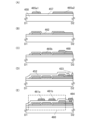
本実施の形態の半導体装置が有するP型トランジスタ及びN型トランジスタを図7に示
す。
<Configuration example>
FIG. 7 shows a P-type transistor and an N-type transistor included in the semiconductor device of this embodiment mode.
図7に示すP型トランジスタ160は、半導体材料を含む基板100に設けられたチャ
ネル形成領域116と、チャネル形成領域116を挟むように設けられた一対の不純物領
域114a、114b及び一対の高濃度不純物領域120a、120b(これらをあわせ
て単に不純物領域とも呼ぶ)と、チャネル形成領域116上に設けられたゲート絶縁層1
08aと、ゲート絶縁層108a上に設けられたゲート電極層110aと、不純物領域1
14aと電気的に接続するソース電極層130aと、不純物領域114bと電気的に接続
するドレイン電極層130bとを有する。
The P-
108a, a
The
なお、ゲート電極層110aの側面にはサイドウォール絶縁層118が設けられている
。また、半導体材料を含む基板100のサイドウォール絶縁層118と重ならない領域に
は、一対の高濃度不純物領域120a、120bを有し、一対の高濃度不純物領域120
a、120b上には一対の金属化合物領域124a、124bが存在する。また、基板1
00上にはP型トランジスタ160を囲むように素子分離絶縁層106が設けられており
、P型トランジスタ160を覆うように、層間絶縁層126および層間絶縁層128が設
けられている。ソース電極層130a、ドレイン電極層130bは、層間絶縁層126お
よび層間絶縁層128に形成された開口を通じて、一対の金属化合物領域124a、12
4bの一方と電気的に接続されている。つまり、ソース電極層130aは、金属化合物領
域124aを介して高濃度不純物領域120aおよび不純物領域114aと電気的に接続
され、ドレイン電極層130bは、金属化合物領域124bを介して高濃度不純物領域1
20bおよび不純物領域114bと電気的に接続されている。
Note that a
A pair of
An element
That is, the
20b and
また、後述するN型トランジスタ164の下層には、ゲート絶縁層108aと同一材料
からなる絶縁層108b、ゲート電極層110aと同一材料からなる電極層110b、並
びにソース電極層130a及びドレイン電極層130bと同一材料からなる電極層130
cが設けられている。
In addition, an insulating
c is provided.
図7に示すN型トランジスタ164は、層間絶縁層128上に設けられたゲート電極層
136dと、ゲート電極層136d上に設けられたゲート絶縁層138と、ゲート絶縁層
138上に設けられた酸化物半導体層140と、酸化物半導体層140上に設けられ、酸
化物半導体層140と電気的に接続されているソース電極層142aと、ドレイン電極層
142bとを有する。
An N-
ここで、ゲート電極層136dは、層間絶縁層128上に形成された絶縁層132に、
埋め込むように設けられている。また、ゲート電極層136dと同様に、P型トランジス
タ160が有する、ソース電極層130aに接する電極層136a及びドレイン電極層1
30bに接する電極層136bが形成されている。また、電極層130cに接する電極層
136cが形成されている。
Here, the
Similarly to the
An
また、N型トランジスタ164の上には、酸化物半導体層140の一部と接するように
、保護絶縁層144が設けられており、保護絶縁層144上には層間絶縁層146が設け
られている。ここで、保護絶縁層144および層間絶縁層146には、ソース電極層14
2a及びドレイン電極層142bにまで達する開口が設けられており、当該開口を通じて
、ソース電極層142aに接する電極層150d、ドレイン電極層142bに接する電極
層150eが形成されている。また、電極層150d、電極層150eと同様に、ゲート
絶縁層138、保護絶縁層144、層間絶縁層146に設けられた開口を通じて、電極層
136aに接する電極層150a、電極層136bに接する電極層150b、及び電極層
136cに接する電極層150cが形成されている。
In addition, a protective
An
ここで、酸化物半導体層140は水素などの不純物が十分に除去され、高純度化されて
いる。具体的には、酸化物半導体層140の水素濃度は5×10¹⁹(atoms/cm
3)以下である。なお、酸化物半導体層140の水素濃度は、5×10¹⁸(atoms
/cm3)以下であることが望ましく、5×1017(atoms/cm3)以下である
ことがより望ましい。水素濃度が十分に低減されて高純度化された酸化物半導体層140
を用いることで、極めて優れたオフ電流特性のN型トランジスタ164を得ることができ
る。このように、水素濃度が十分に低減されて高純度化された酸化物半導体層140を適
用することで、N型トランジスタ164のリーク電流を低減することができる。なお、上
述の酸化物半導体層140中の水素濃度は、二次イオン質量分析法(SIMS:Seco
ndary Ion Mass Spectrometry)で測定したものである。
Here, impurities such as hydrogen are sufficiently removed from the
Note that the hydrogen concentration in the
The hydrogen concentration in the
By using the
The measurements were performed using a direct ion mass spectrometry (DIRMS).
また、層間絶縁層146上には絶縁層152が設けられており、絶縁層152に埋め込
まれるように、電極層154a、電極層154b、電極層154c、電極層154dが設
けられている。なお、電極層154aは電極層150aと接しており、電極層154bは
電極層150bと接しており、電極層154cは電極層150cおよび電極層150dと
接しており、電極層154dは電極層150eと接している。
Moreover, an insulating
本実施の形態で示すP型トランジスタ160が有するソース電極層130aは、上層領
域に設けられた電極層136a、電極層150a、及び電極層154aに電気的に接続し
ている。そのため、P型トランジスタ160のソース電極層130aは、これらの導電層
を適宜形成することにより、上層領域に設けられたN型トランジスタ164が有する電極
層のいずれかと電気的に接続させることが可能である。また、P型トランジスタが有する
ドレイン電極層130bについても同様に、上層領域に設けられたN型トランジスタ16
4が有する電極層のいずれかと電気的に接続させることが可能である。なお、図7には図
示していないが、P型トランジスタ160が有するゲート電極層110aが、上層領域に
設けられた電極層を介して、N型トランジスタ164が有する電極層のいずれかと電気的
に接続する構成にすることもできる。
The
7, the
同様に、本実施の形態で示すN型トランジスタ164が有するソース電極層142aは
、下層領域に設けられた電極層130c及び電極層110bに電気的に接続している。そ
のため、N型トランジスタ164のソース電極層130aは、これらの導電層を適宜形成
することにより、下層領域に設けられたP型トランジスタ160のゲート電極層142a
、ソース電極層130a、又はドレイン電極層130bと電気的に接続させることが可能
である。なお、図7には図示していないが、N型トランジスタ164が有するゲート電極
層136d又はドレイン電極層142bが、下層領域に設けられた電極層を介して、P型
トランジスタ160が有する電極層のいずれかと電気的に接続する構成にすることもでき
る。
Similarly, the
7, the
上述したP型トランジスタ160及びN型トランジスタ164を適宜設けることによっ
て、各種回路を構成することができる。なお、当該回路が有するN型トランジスタ164
の全てを酸化物半導体を用いて形成されるトランジスタとする必要はなく、各トランジス
タに求められる特性に応じて、適宜変更することが可能である。例えば、半導体装置が有
する論理ゲートを構成するN型トランジスタとして、半導体材料を含む基板を用いて形成
されるトランジスタを適用し、当該論理ゲートと、電池の陰極との電気的な接続を制御す
るN型トランジスタとして、酸化物半導体を用いて形成されるトランジスタを適用するこ
とが可能である。
By appropriately providing the above-mentioned P-
For example, a transistor formed using a substrate containing a semiconductor material can be used as an N-type transistor constituting a logic gate of a semiconductor device, and a transistor formed using an oxide semiconductor can be used as an N-type transistor for controlling an electrical connection between the logic gate and a cathode of a battery.
<作製工程例>
次に、P型トランジスタ160及びN型トランジスタ164の作製方法の一例について
説明する。以下では、はじめにP型トランジスタ160の作製方法について図8を参照し
て説明し、その後、N型トランジスタ164の作製方法について図9および図10を参照
して説明する。
<Example of manufacturing process>
Next, an example of a method for manufacturing the P-
まず、半導体材料を含む基板100を用意する(図8(A)参照)。半導体材料を含む
基板100としては、シリコンや炭化シリコンなどの単結晶半導体基板、多結晶半導体基
板、シリコンゲルマニウムなどの化合物半導体基板、SOI基板などを適用することがで
きる。ここでは、半導体材料を含む基板100として、単結晶シリコン基板を用いる場合
の一例について示すものとする。なお、一般に「SOI基板」は、絶縁表面上にシリコン
半導体層が設けられた構成の基板をいうが、本明細書等においては、絶縁表面上にシリコ
ン以外の材料からなる半導体層が設けられた構成の基板をも含む概念として用いる。つま
り、「SOI基板」が有する半導体層は、シリコン半導体層に限定されない。また、SO
I基板には、ガラス基板などの絶縁基板上に絶縁層を介して半導体層が設けられた構成も
含まれるものとする。
First, a
The I substrate also includes a configuration in which a semiconductor layer is provided on an insulating substrate such as a glass substrate via an insulating layer.
基板100上には、素子分離絶縁層を形成するためのマスクとなる保護層102を形成
する(図8(A)参照)。保護層102としては、例えば、酸化シリコンや窒化シリコン
、窒化酸化シリコンなどを材料とする絶縁層を用いることができる。なお、この工程の前
後において、半導体装置のしきい値電圧を制御するために、n型の導電性を付与する不純
物元素やp型の導電性を付与する不純物元素を基板100に添加してもよい。半導体がシ
リコンの場合、n型の導電性を付与する不純物としては、例えば、リンや砒素などを用い
ることができる。また、p型の導電性を付与する不純物としては、例えば、硼素、アルミ
ニウム、ガリウムなどを用いることができる。
A
次に、上記の保護層102をマスクとしてエッチングを行い、保護層102に覆われて
いない領域(露出している領域)の基板100の一部を除去する。これにより分離された
半導体領域104が形成される(図8(B)参照)。当該エッチングには、ドライエッチ
ングを用いるのが好適であるが、ウェットエッチングを用いても良い。エッチングガスや
エッチング液については被エッチング材料に応じて適宜選択することができる。
Next, etching is performed using the
次に、半導体領域104を覆うように絶縁層を形成し、半導体領域104に重畳する領
域の絶縁層を選択的に除去することで、素子分離絶縁層106を形成する(図8(B)参
照)。当該絶縁層は、酸化シリコンや窒化シリコン、窒化酸化シリコンなどを用いて形成
される。絶縁層の除去方法としては、CMP(Chemical Mechanical
Polishing)などの研磨処理やエッチング処理などがあるが、そのいずれを用
いても良い。なお、半導体領域104の形成後、または、素子分離絶縁層106の形成後
には、上記保護層102を除去する。
Next, an insulating layer is formed so as to cover the
Any of the polishing treatments such as polishing (polishing) and etching treatments may be used. After the
次に、半導体領域104上に絶縁層を形成し、当該絶縁層上に導電材料を含む層を形成
する。
Next, an insulating layer is formed over the
絶縁層は後のゲート絶縁層となるものであり、CVD法やスパッタリング法等を用いて
得られる酸化シリコン、窒化酸化シリコン、窒化シリコン、酸化ハフニウム、酸化アルミ
ニウム、酸化タンタル等を含む膜の単層構造または積層構造とすると良い。他に、高密度
プラズマ処理や熱酸化処理によって、半導体領域104の表面を酸化、窒化することによ
り、上記絶縁層を形成してもよい。高密度プラズマ処理は、例えば、He、Ar、Kr、
Xeなどの希ガスと、酸素、酸化窒素、アンモニア、窒素、水素などとの混合ガスを用い
て行うことができる。また、絶縁層の厚さは特に限定されないが、例えば、1nm以上1
00nm以下とすることができる。
The insulating layer is to be a gate insulating layer later, and may have a single-layer structure or a multi-layer structure of a film containing silicon oxide, silicon nitride oxide, silicon nitride, hafnium oxide, aluminum oxide, tantalum oxide, or the like obtained by a CVD method, a sputtering method, or the like. Alternatively, the insulating layer may be formed by oxidizing or nitriding the surface of the
The insulating layer may be formed by using a mixed gas of a rare gas such as Xe, oxygen, nitrogen oxide, ammonia, nitrogen, hydrogen, etc. The thickness of the insulating layer is not particularly limited, but may be, for example, 1 nm or more and 100 nm or less.
00 nm or less.
導電材料を含む層は、アルミニウムや銅、チタン、タンタル、タングステン等の金属材
料を用いて形成することができる。また、導電材料を含む多結晶シリコンなどの半導体材
料を用いて、導電材料を含む層を形成しても良い。形成方法も特に限定されず、蒸着法、
CVD法、スパッタリング法、スピンコート法などの各種成膜方法を用いることができる
。なお、本実施の形態では、導電材料を含む層を、金属材料を用いて形成する場合の一例
について示すものとする。
The layer containing a conductive material can be formed using a metal material such as aluminum, copper, titanium, tantalum, or tungsten. Alternatively, a semiconductor material such as polycrystalline silicon containing a conductive material may be used to form the layer containing a conductive material. The method of formation is not particularly limited, and examples thereof include deposition methods,
Various deposition methods such as a CVD method, a sputtering method, a spin coating method, etc. Note that in this embodiment mode, an example in which a layer containing a conductive material is formed using a metal material will be described.
その後、絶縁層および導電材料を含む層を選択的にエッチングして、ゲート絶縁層10
8a、ゲート電極層110aを形成する(図8(C)参照)。
Thereafter, the insulating layer and the layer containing the conductive material are selectively etched to form the
8a, a
次に、ゲート電極層110aを覆う絶縁層112を形成する(図8(C)参照)。そし
て、半導体領域104に硼素(B)やアルミニウム(Al)などを添加して、浅い接合深
さの一対の不純物領域114a、114bを形成する(図8(C)参照)。なお、ここで
はP型トランジスタを形成するために硼素やアルミニウムを添加しているが、N型トラン
ジスタを形成する場合には、リン(P)やヒ素(As)などの不純物元素を添加すればよ
い。なお、一対の不純物領域114a、114bの形成により、半導体領域104のゲー
ト絶縁層108a下部には、チャネル形成領域116が形成される(図8(C)参照)。
ここで、添加する不純物の濃度は適宜設定することができるが、半導体素子が高度に微細
化される場合には、その濃度を高くすることが望ましい。また、ここでは、絶縁層112
を形成した後に一対の不純物領域114a、114bを形成する工程を採用しているが、
一対の不純物領域114a、114bを形成した後に絶縁層112を形成する工程として
も良い。
Next, an insulating
Here, the concentration of the added impurity can be set as appropriate, but in the case where the semiconductor element is highly miniaturized, it is preferable to increase the concentration.
After forming the first impurity region, a pair of
The insulating
次に、サイドウォール絶縁層118を形成する(図8(D)参照)。サイドウォール絶
縁層118は、絶縁層112を覆うように絶縁層を形成した後に、当該絶縁層に異方性の
高いエッチング処理を適用することで、自己整合的に形成することができる。また、この
際に、絶縁層112を部分的にエッチングして、ゲート電極層110aの上面と、一対の
不純物領域114a、114bの上面を露出させると良い。
Next, the
次に、ゲート電極層110a、一対の不純物領域114a、114b、サイドウォール
絶縁層118等を覆うように、絶縁層を形成する。そして、一対の不純物領域114a、
114bの一部に対して硼素(B)やアルミニウム(Al)などを添加して、一対の高濃
度不純物領域120a、120bを形成する(図8(E)参照)。ここでも、N型トラン
ジスタを形成する場合には、リン(P)やヒ素(As)などの不純物元素を添加すればよ
い。その後、上記絶縁層を除去し、ゲート電極層110a、サイドウォール絶縁層118
、一対の高濃度不純物領域120a、120b等を覆うように金属層122を形成する(
図8(E)参照)。金属層122は、真空蒸着法やスパッタリング法、スピンコート法な
どの各種成膜方法を用いて形成することができる。金属層122は、半導体領域104を
構成する半導体材料と反応して低抵抗な金属化合物となる金属材料を用いて形成すること
が望ましい。このような金属材料としては、例えば、チタン、タンタル、タングステン、
ニッケル、コバルト、白金等がある。
Next, an insulating layer is formed so as to cover the
Boron (B), aluminum (Al), or the like is added to a part of the insulating
A
(See FIG. 8E). The
Examples include nickel, cobalt, and platinum.
次に、熱処理を施して、金属層122と半導体材料とを反応させる。これにより、一対
の高濃度不純物領域120a、120bに接する一対の金属化合物領域124a、124
bが形成される(図8(F)参照)。なお、ゲート電極層110aとして多結晶シリコン
などを用いる場合には、ゲート電極層110aの金属層122と接触する部分にも、金属
化合物領域が形成されることになる。
Next, a heat treatment is performed to react the
In the case where polycrystalline silicon or the like is used for the
上記熱処理としては、例えば、フラッシュランプの照射による熱処理を用いることがで
きる。もちろん、その他の熱処理方法を用いても良いが、金属化合物の形成に係る化学反
応の制御性を向上させるためには、ごく短時間の熱処理が実現できる方法を用いることが
望ましい。なお、上記の金属化合物領域は、金属材料と半導体材料との反応により形成さ
れるものであり、十分に導電性が高められた領域である。当該金属化合物領域を形成する
ことで、電気抵抗を十分に低減し、素子特性を向上させることができる。なお、一対の金
属化合物領域124a、124bを形成した後には、金属層122は除去する。
The heat treatment may be, for example, a heat treatment by irradiation with a flash lamp. Of course, other heat treatment methods may be used, but in order to improve the controllability of the chemical reaction involved in the formation of the metal compound, it is desirable to use a method that can realize a heat treatment for a very short time. The metal compound region is formed by the reaction between a metal material and a semiconductor material, and is a region with sufficiently high conductivity. By forming the metal compound region, the electrical resistance can be sufficiently reduced and the element characteristics can be improved. After forming the pair of
次に、上述の工程により形成された各構成を覆うように、層間絶縁層126、層間絶縁
層128を形成する(図8(G)参照)。層間絶縁層126や層間絶縁層128は、酸化
シリコン、窒化酸化シリコン、窒化シリコン、酸化ハフニウム、酸化アルミニウム、酸化
タンタル等の無機絶縁材料を含む材料を用いて形成することができる。また、ポリイミド
、アクリル等の有機絶縁材料を用いて形成することも可能である。なお、ここでは、層間
絶縁層126や層間絶縁層128の二層構造としているが、層間絶縁層の構成はこれに限
定されない。層間絶縁層128の形成後には、その表面を、CMPやエッチング処理など
によって平坦化しておくことが望ましい。
Next, the
その後、上記層間絶縁層に、一対の金属化合物領域124a、124bにまで達する開
口を形成し、当該開口に、ソース電極層130a、ドレイン電極層130bを形成する(
図8(H)参照)。ソース電極層130a及びドレイン電極層130bは、例えば、開口
を含む領域にPVD法やCVD法などを用いて導電層を形成した後、エッチング処理やC
MPといった方法を用いて、上記導電層の一部を除去することにより形成することができ
る。
Thereafter, openings reaching the pair of
The
It can be formed by removing a part of the conductive layer using a method such as MP.
なお、ソース電極層130a及びドレイン電極層130bを形成する際には、その表面
が平坦になるように加工することが望ましい。例えば、開口を含む領域にチタン膜や窒化
チタン膜を薄く形成した後に、開口に埋め込むようにタングステン膜を形成する場合には
、その後のCMPによって、不要なタングステン、チタン、窒化チタンなどを除去すると
共に、その表面の平坦性を向上させることができる。このように、ソース電極層130a
及びドレイン電極層130bを含む表面を平坦化することにより、後の工程において、良
好な電極、配線、絶縁層、半導体層などを形成することが可能となる。
Note that, when the
By planarizing the surface including the
なお、ここでは、一対の金属化合物領域124a、124bと接触するソース電極層1
30a及びドレイン電極層130bのみを示しているが、この工程において、配線として
機能する電極層(例えば、図7における電極層130c)などをあわせて形成することが
できる。ソース電極層130a及びドレイン電極層130bとして用いることができる材
料について特に限定はなく、各種導電材料を用いることができる。例えば、モリブデン、
チタン、クロム、タンタル、タングステン、アルミニウム、銅、ネオジム、スカンジウム
などの導電性材料を用いることができる。
In this case, the
Although only the
Conductive materials such as titanium, chromium, tantalum, tungsten, aluminum, copper, neodymium, and scandium can be used.
以上により、半導体材料を含む基板100を用いたP型トランジスタ160が形成され
る。なお、上記工程の後には、さらに電極や配線、絶縁層などを形成しても良い。配線の
構造として、層間絶縁層および導電層の積層構造でなる多層配線構造を採用することによ
り、高度に集積化した回路を提供することができる。また、上記工程と同様の工程によっ
て、半導体材料を含む基板100を用いたN型トランジスタも形成することが可能である
。すなわち、上述した工程において、半導体領域に添加する不純物元素をリン(P)やヒ
素(As)などの不純物元素に変更することによって、N型トランジスタを形成すること
ができる。
As a result, a P-
次に、図9および図10を用いて、層間絶縁層128上にN型トランジスタ164を作
製する工程について説明する。なお、図9および図10は、層間絶縁層128上の各種電
極層や、N型トランジスタ164などの作製工程を示すものであるから、N型トランジス
タ164の下部に存在するP型トランジスタ160等については省略している。
Next, a process for fabricating an N-
まず、層間絶縁層128、ソース電極層130a、ドレイン電極層130b、電極層1
30c上に絶縁層132を形成する(図9(A)参照)。絶縁層132はPVD法やCV
D法などを用いて形成することができる。また、酸化シリコン、窒化酸化シリコン、窒化
シリコン、酸化ハフニウム、酸化アルミニウム、酸化タンタル等の無機絶縁材料を含む材
料を用いて形成することができる。
First, the
An insulating
The insulating film can be formed by a method such as Method D. The insulating film can also be formed using a material containing an inorganic insulating material such as silicon oxide, silicon nitride oxide, silicon nitride, hafnium oxide, aluminum oxide, or tantalum oxide.
次に、絶縁層132に対し、ソース電極層130a、ドレイン電極層130b、および
電極層130cにまで達する開口を形成する。この際、後にゲート電極層136dが形成
される領域にも併せて開口を形成する。そして、上記開口に埋め込むように、導電層13
4を形成する(図9(B)参照)。上記開口はマスクを用いたエッチングなどの方法で形
成することができる。当該マスクは、フォトマスクを用いた露光などの方法によって形成
することが可能である。エッチングとしてはウェットエッチング、ドライエッチングのい
ずれを用いても良いが、微細加工の観点からは、ドライエッチングを用いることが好適で
ある。導電層134の形成は、PVD法やCVD法などの成膜法を用いて行うことができ
る。導電層134の形成に用いることができる材料としては、モリブデン、チタン、クロ
ム、タンタル、タングステン、アルミニウム、銅、ネオジム、スカンジウムなどの導電性
材料や、これらの合金、化合物(例えば窒化物)などが挙げられる。
Next, openings are formed in the insulating
4 is formed (see FIG. 9B). The opening can be formed by a method such as etching using a mask. The mask can be formed by a method such as exposure using a photomask. Either wet etching or dry etching can be used as the etching, but dry etching is preferably used from the viewpoint of fine processing. The
より具体的には、例えば、開口を含む領域にPVD法によりチタン膜を薄く形成し、C
VD法により窒化チタン膜を薄く形成した後に、開口に埋め込むようにタングステン膜を
形成する方法を適用することができる。ここで、PVD法により形成されるチタン膜は、
界面の酸化膜を還元し、下部電極層(ここでは、ソース電極層130a、ドレイン電極層
130b、電極層130cなど)との接触抵抗を低減させる機能を有する。また、その後
に形成される窒化チタン膜は、導電性材料の拡散を抑制するバリア機能を備える。また、
チタンや窒化チタンなどによるバリア膜を形成した後に、メッキ法により銅膜を形成して
もよい。
More specifically, for example, a thin titanium film is formed in the region including the opening by a PVD method, and C
A method can be applied in which a thin titanium nitride film is formed by the PVD method, and then a tungsten film is formed so as to fill the opening. Here, the titanium film formed by the PVD method is
The titanium nitride film has a function of reducing the oxide film at the interface and reducing the contact resistance with the lower electrode layer (here, the
A copper film may be formed by plating after forming a barrier film made of titanium, titanium nitride, or the like.
導電層134を形成した後には、エッチング処理やCMPといった方法を用いて導電層
134の一部を除去し、絶縁層132を露出させて、電極層136a、電極層136b、
電極層136c、ゲート電極層136dを形成する(図9(C)参照)。なお、上記導電
層134の一部を除去して電極層136a、電極層136b、電極層136c、ゲート電
極層136dを形成する際には、表面が平坦になるように加工することが望ましい。この
ように、絶縁層132、電極層136a、電極層136b、電極層136c、ゲート電極
層136dの表面を平坦化することにより、後の工程において、良好な電極、配線、絶縁
層、半導体層などを形成することが可能となる。
After the
The
次に、絶縁層132、電極層136a、電極層136b、電極層136c、ゲート電極
層136dを覆うように、ゲート絶縁層138を形成する(図9(D)参照)。ゲート絶
縁層138は、CVD法やスパッタリング法等を用いて形成することができる。また、ゲ
ート絶縁層138は、酸化珪素、窒化珪素、酸化窒化珪素、窒化酸化珪素、酸化アルミニ
ウム、酸化ハフニウム、酸化タンタルなどを含むように形成するのが好適である。なお、
ゲート絶縁層138は、単層構造としても良いし、積層構造としても良い。例えば、原料
ガスとして、シラン(SiH4)、酸素、窒素を用いたプラズマCVD法により、酸化窒
化珪素でなるゲート絶縁層138を形成することができる。ゲート絶縁層138の厚さは
特に限定されないが、例えば、10nm以上500nm以下とすることができる。積層構
造の場合は、例えば、膜厚50nm以上200nm以下の第1のゲート絶縁層と、第1の
ゲート絶縁層上の膜厚5nm以上300nm以下の第2のゲート絶縁層の積層とすると好
適である。
Next, a
The
なお、不純物を除去することによりi型化または実質的にi型化された酸化物半導体(
高純度化された酸化物半導体)は、界面準位や界面電荷に対して極めて敏感であるため、
このような酸化物半導体を酸化物半導体層に用いる場合には、ゲート絶縁層との界面は重
要である。つまり、高純度化された酸化物半導体層に接するゲート絶縁層138には、高
品質化が要求されることになる。
Note that an oxide semiconductor that has been made i-type or substantially i-type by removing impurities (
Since the SiO2 semiconductor (a highly purified oxide semiconductor) is extremely sensitive to interface states and interface charges,
When such an oxide semiconductor is used for the oxide semiconductor layer, the interface with the gate insulating layer is important, that is, the
例えば、μ波(2.45GHz)を用いた高密度プラズマCVD法は、緻密で絶縁耐圧
の高い高品質なゲート絶縁層138を形成できる点で好適である。高純度化された酸化物
半導体層と高品質ゲート絶縁層とが密接することにより、界面準位を低減して界面特性を
良好なものとすることができるからである。
For example, a high density plasma CVD method using microwaves (2.45 GHz) is suitable in that a high quality
もちろん、ゲート絶縁層として良質な絶縁層を形成できるものであれば、高純度化され
た酸化物半導体層を用いる場合であっても、スパッタリング法やプラズマCVD法など他
の方法を適用することができる。また、形成後の熱処理によって、膜質や界面特性が改質
される絶縁層を適用しても良い。いずれにしても、ゲート絶縁層138としての膜質が良
好であると共に、酸化物半導体層との界面準位密度を低減し、良好な界面を形成できるゲ
ート絶縁層138を形成すれば良い。
Of course, even when a highly purified oxide semiconductor layer is used, other methods such as a sputtering method or a plasma CVD method can be applied as long as a good-quality insulating layer can be formed as the gate insulating layer. Alternatively, an insulating layer whose film quality or interface characteristics are improved by heat treatment after formation may be applied. In any case, it is sufficient to form the
さらに、85℃、2×10⁶(V/cm)、12時間のゲートバイアス・熱ストレス試
験(BT試験)においては、不純物が酸化物半導体に添加されていると、不純物と酸化物
半導体の主成分との結合手が、強電界(B:バイアス)と高温(T:温度)により切断さ
れ、生成された未結合手がしきい値電圧(Vth)のドリフトを誘発することとなる。
Furthermore, in a gate bias thermal stress test (BT test) at 85° C., 2×10 6 (V/cm), and 12 hours, when impurities are added to an oxide semiconductor, bonds between the impurities and the main components of the oxide semiconductor are cut by a strong electric field (B: bias) and high temperature (T: temperature), and the generated dangling bonds induce a drift of the threshold voltage (Vth).
これに対して、酸化物半導体の不純物、特に水素や水などを極力排除し、上記のように
ゲート絶縁層との界面特性を良好にすることにより、BT試験に対しても安定なトランジ
スタを得ることが可能である。
In response to this, impurities in the oxide semiconductor, particularly hydrogen and water, are eliminated as much as possible, and the interface characteristics with the gate insulating layer are improved as described above, whereby a transistor that is stable even in a BT test can be obtained.
次いで、ゲート絶縁層138上に、酸化物半導体層を形成し、マスクを用いたエッチン
グなどの方法によって該酸化物半導体層を加工して、島状の酸化物半導体層140を形成
する(図9(E)参照)。
Next, an oxide semiconductor layer is formed over the
酸化物半導体層としては、In-Ga-Zn-O系、In-Sn-Zn-O系、In-
Al-Zn-O系、Sn-Ga-Zn-O系、Al-Ga-Zn-O系、Sn-Al-Z
n-O系、In-Zn-O系、Sn-Zn-O系、Al-Zn-O系、In-O系、Sn
-O系、Zn-O系の酸化物半導体層、特に非晶質酸化物半導体層を用いるのが好適であ
る。本実施の形態では、酸化物半導体層としてIn-Ga-Zn-O系の金属酸化物ター
ゲットを用いて、非晶質の酸化物半導体層をスパッタ法により形成することとする。なお
、非晶質の酸化物半導体層中にシリコンを添加することで、その結晶化を抑制することが
できるから、例えば、SiO2を2重量%以上10重量%以下含むターゲットを用いて酸
化物半導体層を形成しても良い。
The oxide semiconductor layer may be an In-Ga-Zn-O-based, an In-Sn-Zn-O-based, or an In-
Al-Zn-O system, Sn-Ga-Zn-O system, Al-Ga-Zn-O system, Sn-Al-Z
n-O series, In-Zn-O series, Sn-Zn-O series, Al-Zn-O series, In-O series, Sn
It is preferable to use an In—Ga—Zn—O-based oxide semiconductor layer, and particularly an amorphous oxide semiconductor layer. In this embodiment, an In—Ga—Zn—O-based metal oxide target is used as the oxide semiconductor layer, and an amorphous oxide semiconductor layer is formed by a sputtering method. Note that, since crystallization of an amorphous oxide semiconductor layer can be suppressed by adding silicon to the amorphous oxide semiconductor layer, for example, the oxide semiconductor layer may be formed using a target containing SiO 2 in an amount of 2 wt % to 10 wt %.
酸化物半導体層をスパッタリング法で作製するためのターゲットとしては、例えば、酸
化亜鉛などを主成分とする金属酸化物のターゲットを用いることができる。また、In、
Ga、およびZnを含む金属酸化物ターゲット(組成比として、In2O3:Ga2O3
:ZnO=1:1:1[mol比]、In:Ga:Zn=1:1:0.5[atom比]
)などを用いることもできる。また、In、Ga、およびZnを含む金属酸化物ターゲッ
トとして、In:Ga:Zn=1:1:1[atom比]、またはIn:Ga:Zn=1
:1:2[atom比]の組成比を有するターゲットなどを用いても良い。金属酸化物タ
ーゲットの充填率は90%以上100%以下、好ましくは95%以上(例えば99.9%
)である。充填率の高い金属酸化物ターゲットを用いることにより、緻密な酸化物半導体
層が形成される。
As a target for forming the oxide semiconductor layer by a sputtering method, for example, a metal oxide target containing zinc oxide or the like as a main component can be used.
A metal oxide target containing Ga and Zn (composition ratio: In 2 O 3 :Ga 2 O 3
:ZnO=1:1:1 [molar ratio], In:Ga:Zn=1:1:0.5 [atom ratio]
In addition, as a metal oxide target containing In, Ga, and Zn, a target having a ratio of In:Ga:Zn=1:1:1 [atom ratio] or a target having a ratio of In:Ga:Zn=1:1:1 [atom ratio] may be used.
A target having a composition ratio of 0.1:0.2 [atom ratio] may be used. The filling rate of the metal oxide target is 90% or more and 100% or less, preferably 95% or more (for example, 99.9%).
By using a metal oxide target with a high filling rate, a dense oxide semiconductor layer is formed.
酸化物半導体層の形成雰囲気は、希ガス(代表的にはアルゴン)雰囲気、酸素雰囲気、
または、希ガス(代表的にはアルゴン)と酸素との混合雰囲気とするのが好適である。具
体的には、例えば、水素、水、水酸基、水素化物などの不純物が、数ppm程度(望まし
くは数ppb程度)にまで除去された高純度ガスを用いるのが好適である。
The oxide semiconductor layer is formed in a rare gas (typically, argon) atmosphere, an oxygen atmosphere, or
Alternatively, it is preferable to use a mixed atmosphere of a rare gas (typically argon) and oxygen.Specifically, it is preferable to use a high-purity gas in which impurities such as hydrogen, water, hydroxyl groups, and hydrides have been removed to about several ppm (preferably about several ppb).
酸化物半導体層の形成の際には、減圧状態に保持された処理室内に基板を保持し、基板
温度を100℃以上600℃以下好ましくは200℃以上400℃以下とする。基板を加
熱しながら酸化物半導体層を形成することにより、酸化物半導体層に含まれる不純物濃度
を低減することができる。また、スパッタリングによる損傷が軽減される。そして、処理
室内の残留水分を除去しつつ水素および水が除去されたスパッタガスを導入し、金属酸化
物をターゲットとして酸化物半導体層を形成する。処理室内の残留水分を除去するために
は、吸着型の真空ポンプを用いることが好ましい。例えば、クライオポンプ、イオンポン
プ、チタンサブリメーションポンプを用いることができる。また、排気手段としては、タ
ーボポンプにコールドトラップを加えたものであってもよい。クライオポンプを用いて排
気した処理室は、例えば、水素原子、水(H2O)など水素原子を含む化合物(より好ま
しくは炭素原子を含む化合物も)等が排気されるため、当該処理室で形成した酸化物半導
体層に含まれる不純物の濃度を低減できる。
When the oxide semiconductor layer is formed, the substrate is held in a treatment chamber kept under reduced pressure, and the substrate temperature is set to 100° C. to 600° C., preferably 200° C. to 400° C. By forming the oxide semiconductor layer while heating the substrate, the impurity concentration in the oxide semiconductor layer can be reduced. In addition, damage caused by sputtering is reduced. Then, a sputtering gas from which hydrogen and water have been removed is introduced while removing residual moisture in the treatment chamber, and the oxide semiconductor layer is formed using a metal oxide as a target. In order to remove residual moisture in the treatment chamber, it is preferable to use an adsorption type vacuum pump. For example, a cryopump, an ion pump, or a titanium sublimation pump can be used. In addition, the exhaust means may be a turbo pump with a cold trap added thereto. In the treatment chamber evacuated using a cryopump, for example, hydrogen atoms, compounds containing hydrogen atoms such as water (H 2 O) (more preferably compounds containing carbon atoms), and the like are exhausted, so that the impurity concentration in the oxide semiconductor layer formed in the treatment chamber can be reduced.
形成条件としては、例えば、基板とターゲットの間との距離が100mm、圧力が0.
6Pa、直流(DC)電力が0.5kW、雰囲気が酸素(酸素流量比率100%)雰囲気
、といった条件を適用することができる。なお、パルス直流(DC)電源を用いると、成
膜時に発生する粉状物質(パーティクル、ゴミともいう)が軽減でき、膜厚分布も均一と
なるため、好ましい。酸化物半導体層の厚さは、2nm以上200nm以下、好ましくは
5nm以上30nm以下とする。なお、適用する酸化物半導体材料により適切な厚さは異
なるから、その厚さは用いる材料に応じて適宜選択すればよい。
The formation conditions are, for example, a distance between the substrate and the target of 100 mm and a pressure of 0.
The conditions that can be applied are: pressure of 6 Pa, direct current (DC) power of 0.5 kW, and oxygen atmosphere (oxygen flow rate ratio of 100%). Note that using a pulsed direct current (DC) power source is preferable because it can reduce powdery substances (also called particles or dust) generated during film formation and can provide a uniform film thickness distribution. The thickness of the oxide semiconductor layer is 2 nm to 200 nm, preferably 5 nm to 30 nm. Note that the appropriate thickness varies depending on the oxide semiconductor material used, and the thickness may be appropriately selected depending on the material used.
なお、酸化物半導体層をスパッタ法により形成する前には、アルゴンガスを導入してプ
ラズマを発生させる逆スパッタを行い、ゲート絶縁層138の表面に付着しているゴミを
除去するのが好適である。ここで、逆スパッタとは、通常のスパッタにおいては、スパッ
タターゲットにイオンを衝突させるところ、逆に、処理表面にイオンを衝突させることに
よってその表面を改質する方法のことをいう。処理表面にイオンを衝突させる方法として
は、アルゴン雰囲気下で処理表面側に高周波電圧を印加して、基板付近にプラズマを生成
する方法などがある。なお、アルゴン雰囲気に代えて窒素、ヘリウム、酸素などを用いて
も良い。
Note that, before forming the oxide semiconductor layer by a sputtering method, it is preferable to perform reverse sputtering in which argon gas is introduced to generate plasma and to remove dust attached to the surface of the
上記酸化物半導体層のエッチングには、ドライエッチング、ウェットエッチングのいず
れを用いても良い。もちろん、両方を組み合わせて用いることもできる。所望の形状にエ
ッチングできるよう、材料に合わせてエッチング条件(エッチングガスやエッチング液、
エッチング時間、温度等)を適宜設定する。
For etching the oxide semiconductor layer, either dry etching or wet etching may be used. Of course, both may be used in combination. The etching conditions (etching gas, etchant, etc.) are determined according to the material so that the oxide semiconductor layer can be etched into a desired shape.
The etching time, temperature, etc. are set appropriately.
ドライエッチングに用いるエッチングガスには、例えば、塩素を含むガス(塩素系ガス
、例えば塩素(Cl2)、塩化硼素(BCl3)、塩化珪素(SiCl4)、四塩化炭素
(CCl4)など)などがある。また、フッ素を含むガス(フッ素系ガス、例えば四弗化
炭素(CF4)、六弗化硫黄(SF6)、三弗化窒素(NF3)、トリフルオロメタン(
CHF3)など)、臭化水素(HBr)、酸素(O2)、これらのガスにヘリウム(He
)やアルゴン(Ar)などの希ガスを添加したガス、などを用いても良い。
Etching gases used in dry etching include, for example, gases containing chlorine (chlorine-based gases, such as chlorine (Cl 2 ), boron chloride (BCl 3 ), silicon chloride (SiCl 4 ), carbon tetrachloride (CCl 4 ), etc.), and gases containing fluorine (fluorine-based gases, such as carbon tetrafluoride (CF 4 ), sulfur hexafluoride (SF 6 ), nitrogen trifluoride (NF 3 ), trifluoromethane (
CHF 3 ), hydrogen bromide (HBr), oxygen (O 2 ), and helium (He
), or a gas containing a rare gas such as argon (Ar), etc. may also be used.
ドライエッチング法としては、平行平板型RIE(Reactive Ion Etc
hing)法や、ICP(Inductively Coupled Plasma:誘
導結合型プラズマ)エッチング法を用いることができる。所望の形状にエッチングできる
ように、エッチング条件(コイル型の電極に印加される電力量、基板側の電極に印加され
る電力量、基板側の電極温度等)は適宜設定する。
As a dry etching method, parallel plate type RIE (Reactive Ion Etc.
In order to etch into a desired shape, the etching conditions (such as the amount of power applied to the coil-shaped electrode, the amount of power applied to the electrode on the substrate side, and the temperature of the electrode on the substrate side) are appropriately set.
ウェットエッチングに用いるエッチング液としては、燐酸と酢酸と硝酸を混ぜた溶液な
どを用いることができる。また、ITO07N(関東化学社製)などのエッチング液を用
いてもよい。
The etching solution used for the wet etching may be a mixture of phosphoric acid, acetic acid, and nitric acid, or may be ITO07N (manufactured by Kanto Chemical Co., Ltd.).
次いで、酸化物半導体層に第1の熱処理を行うことが望ましい。この第1の熱処理によ
って酸化物半導体層の脱水化または脱水素化を行うことができる。第1の熱処理の温度は
、300℃以上750℃以下、好ましくは400℃以上基板の歪み点未満とする。例えば
、抵抗発熱体などを用いた電気炉に基板を導入し、酸化物半導体層140に対して窒素雰
囲気下450℃において1時間の熱処理を行う。この間、酸化物半導体層140は、大気
に触れることなく、水や水素の再混入が行われないようにする。
Next, it is preferable to perform a first heat treatment on the oxide semiconductor layer. The first heat treatment can dehydrate or dehydrogenate the oxide semiconductor layer. The temperature of the first heat treatment is 300° C. or higher and 750° C. or lower, preferably 400° C. or higher and lower than the strain point of the substrate. For example, the substrate is placed in an electric furnace using a resistance heating element or the like, and the
なお、熱処理装置は電気炉に限られず、加熱されたガスなどの媒体からの熱伝導、また
は熱輻射によって、被処理物を加熱する装置であっても良い。例えば、GRTA(Gas
Rapid Thermal Anneal)装置、LRTA(Lamp Rapid
Thermal Anneal)装置等のRTA(Rapid Thermal An
neal)装置を用いることができる。LRTA装置は、ハロゲンランプ、メタルハライ
ドランプ、キセノンアークランプ、カーボンアークランプ、高圧ナトリウムランプ、高圧
水銀ランプなどのランプから発する光(電磁波)の輻射により、被処理物を加熱する装置
である。GRTA装置は、高温のガスを用いて熱処理を行う装置である。気体としては、
アルゴンなどの希ガス、または窒素のような、熱処理によって被処理物と反応しない不活
性気体が用いられる。
The heat treatment device is not limited to an electric furnace, and may be a device that heats the workpiece by thermal conduction or thermal radiation from a medium such as a heated gas.
Rapid Thermal Anneal) device, LRTA (Lamp Rapid
RTA (Rapid Thermal Anneal) equipment, etc.
A LRTA apparatus is an apparatus that heats the workpiece by radiating light (electromagnetic waves) emitted from a lamp such as a halogen lamp, a metal halide lamp, a xenon arc lamp, a carbon arc lamp, a high-pressure sodium lamp, or a high-pressure mercury lamp. A GRTA apparatus is an apparatus that performs heat treatment using a high-temperature gas. The gas may be, for example,
An inert gas that does not react with the object to be treated by heat treatment, such as a rare gas such as argon or nitrogen, is used.
例えば、第1の熱処理として、650℃~700℃の高温に加熱した不活性ガス中に基
板を投入し、数分間加熱した後、当該不活性ガス中から基板を取り出すGRTA処理を行
ってもよい。GRTA処理を用いると短時間での高温熱処理が可能となる。また、短時間
の熱処理であるため、基板の歪み点を超える温度条件であっても適用が可能となる。
For example, the first heat treatment may be a GRTA treatment in which the substrate is placed in an inert gas heated to a high temperature of 650° C. to 700° C., heated for several minutes, and then removed from the inert gas. The GRTA treatment enables high-temperature heat treatment in a short time. In addition, because it is a short-time heat treatment, it can be applied even under temperature conditions exceeding the distortion point of the substrate.
なお、第1の熱処理は、窒素、または希ガス(ヘリウム、ネオン、アルゴン等)を主成
分とする雰囲気であって、水、水素などが含まれない雰囲気で行うことが望ましい。例え
ば、熱処理装置に導入する窒素、またはヘリウム、ネオン、アルゴン等の希ガスの純度を
、6N(99.9999%)以上、好ましくは7N(99.99999%)以上(すなわ
ち、不純物濃度が1ppm以下、好ましくは0.1ppm以下)とする。
The first heat treatment is desirably performed in an atmosphere containing nitrogen or a rare gas (helium, neon, argon, etc.) as a main component and not containing water, hydrogen, etc. For example, the purity of nitrogen or a rare gas such as helium, neon, argon, etc. introduced into the heat treatment apparatus is set to 6N (99.9999%) or more, preferably 7N (99.99999%) or more (i.e., the impurity concentration is 1 ppm or less, preferably 0.1 ppm or less).
第1の熱処理の条件、または酸化物半導体層の材料によっては、酸化物半導体層が結晶
化し、微結晶または多結晶となる場合もある。例えば、結晶化率が90%以上、または8
0%以上の微結晶の酸化物半導体層となる場合もある。また、第1の熱処理の条件、また
は酸化物半導体層の材料によっては、結晶成分を含まない非晶質の酸化物半導体層となる
場合もある。
Depending on the conditions of the first heat treatment or the material of the oxide semiconductor layer, the oxide semiconductor layer may be crystallized to become microcrystalline or polycrystalline.
Depending on the conditions of the first heat treatment or the material of the oxide semiconductor layer, the oxide semiconductor layer may be an amorphous oxide semiconductor layer containing no crystalline component.
また、非晶質の酸化物半導体(例えば、酸化物半導体層の表面)に微結晶(粒径1nm
以上20nm以下(代表的には2nm以上4nm以下))が混在する酸化物半導体層とな
る場合もある。
In addition, microcrystals (
In some cases, the oxide semiconductor layer may have a thickness of more than 20 nm (typically more than 2 nm and less than 4 nm).
また、非晶質中に微結晶を配列させることで、酸化物半導体層の電気的特性を変化させ
ることも可能である。例えば、In-Ga-Zn-O系の金属酸化物ターゲットを用いて
酸化物半導体層を形成する場合には、電気的異方性を有するIn2Ga2ZnO7の結晶
粒が配向した微結晶部を形成することで、酸化物半導体層の電気的特性を変化させること
ができる。
In addition, the electrical characteristics of the oxide semiconductor layer can be changed by arranging microcrystals in an amorphous material. For example, when an oxide semiconductor layer is formed using an In-Ga-Zn-O-based metal oxide target, the electrical characteristics of the oxide semiconductor layer can be changed by forming a microcrystal portion in which crystal grains of In 2 Ga 2 ZnO 7 having electrical anisotropy are aligned.
より具体的には、例えば、In2Ga2ZnO7のc軸が酸化物半導体層の表面に垂直
な方向をとるように配向させることで、酸化物半導体層の表面に平行な方向の導電性を向
上させ、酸化物半導体層の表面に垂直な方向の絶縁性を向上させることができる。また、
このような微結晶部は、酸化物半導体層中への水や水素などの不純物の侵入を抑制する機
能を有する。
More specifically, for example, by orienting the c-axis of In 2 Ga 2 ZnO 7 in a direction perpendicular to the surface of the oxide semiconductor layer, the electrical conductivity in a direction parallel to the surface of the oxide semiconductor layer can be improved, and the insulating property in a direction perpendicular to the surface of the oxide semiconductor layer can be improved.
Such a microcrystal portion has a function of suppressing entry of impurities such as water or hydrogen into the oxide semiconductor layer.
なお、上述の微結晶部を有する酸化物半導体層は、GRTA処理による酸化物半導体層
の表面加熱によって形成することができる。また、Znの含有量がInまたはGaの含有
量より小さいスパッタターゲットを用いることで、より好適に形成することが可能である
。
The oxide semiconductor layer having the above-described microcrystalline portion can be formed by heating the surface of the oxide semiconductor layer through GRTA treatment. In addition, the oxide semiconductor layer can be more suitably formed by using a sputtering target in which the Zn content is smaller than the In content or the Ga content.
酸化物半導体層140に対する第1の熱処理は、島状の酸化物半導体層140に加工す
る前の酸化物半導体層に行うこともできる。その場合には、第1の熱処理後に、加熱装置
から基板を取り出し、フォトリソグラフィ工程を行うことになる。
The first heat treatment for the
なお、上記熱処理は、酸化物半導体層140に対する脱水化、脱水素化の効果があるか
ら、脱水化処理、脱水素化処理などと呼ぶこともできる。このような脱水化処理、脱水素
化処理は、酸化物半導体層の形成後、酸化物半導体層140上にソース電極層及びドレイ
ン電極層を積層させた後、又はソース電極層及びドレイン電極層上に保護絶縁層を形成し
た後、などのタイミングにおいて行うことが可能である。また、このような脱水化処理、
脱水素化処理は、一回に限らず複数回行っても良い。
Note that the heat treatment can also be called a dehydration treatment, a dehydrogenation treatment, or the like because it has an effect of dehydrating or dehydrogenating the
The dehydrogenation treatment may be carried out not only once but also multiple times.
次に、酸化物半導体層140に接するように、ソース電極層142a及びドレイン電極
層142bを形成する(図9(F)参照)。ソース電極層142a及びドレイン電極層1
42bは、酸化物半導体層140を覆うように導電層を形成した後、当該導電層を選択的
にエッチングすることにより形成することができる。
Next, the
The portion 42b can be formed by forming a conductive layer to cover the
当該導電層は、スパッタ法などのPVD法や、プラズマCVD法などのCVD法を用い
て形成することができる。また、導電層の材料としては、アルミニウム、クロム、銅、タ
ンタル、チタン、モリブデン、タングステンからから選ばれた元素や、上述した元素を成
分とする合金等を用いることができる。マンガン、マグネシウム、ジルコニウム、ベリリ
ウム、トリウムのいずれか一または複数から選択された材料を用いてもよい。また、アル
ミニウムに、チタン、タンタル、タングステン、モリブデン、クロム、ネオジム、スカン
ジウムから選ばれた元素を単数、または複数組み合わせた材料を用いてもよい。導電層は
、単層構造であっても良いし、2層以上の積層構造としてもよい。例えば、シリコンを含
むアルミニウム膜の単層構造、アルミニウム膜上にチタン膜が積層された2層構造、チタ
ン膜とアルミニウム膜とチタン膜とが積層された3層構造などが挙げられる。
The conductive layer can be formed by using a PVD method such as a sputtering method or a CVD method such as a plasma CVD method. In addition, as a material of the conductive layer, an element selected from aluminum, chromium, copper, tantalum, titanium, molybdenum, and tungsten, an alloy containing the above-mentioned element, or the like can be used. A material selected from any one or more of manganese, magnesium, zirconium, beryllium, and thorium may be used. In addition, a material in which a single element selected from titanium, tantalum, tungsten, molybdenum, chromium, neodymium, and scandium is combined with aluminum, or a combination of a single element and a plurality of elements may be used. The conductive layer may have a single layer structure or a stacked structure of two or more layers. For example, a single layer structure of an aluminum film containing silicon, a two-layer structure in which a titanium film is stacked on an aluminum film, and a three-layer structure in which a titanium film, an aluminum film, and a titanium film are stacked, and the like can be used.
ここで、エッチングに用いるマスク形成時の露光には、紫外線やKrFレーザ光やAr
Fレーザ光を用いるのが好適である。
Here, the exposure for forming the mask used for etching is performed using ultraviolet light, KrF laser light, or Ar.
It is preferable to use F laser light.
トランジスタのチャネル長(L)は、ソース電極層142aの下端部と、ドレイン電極
層142bの下端部との間隔によって決定される。なお、チャネル長(L)が25nm未
満の露光を行う場合には、数nm~数10nmと極めて波長が短い超紫外線(Extre
me Ultraviolet)を用いてマスク形成の露光を行う。超紫外線による露光
は、解像度が高く焦点深度も大きい。従って、後に形成されるトランジスタのチャネル長
(L)を10nm以上1000nm以下とすることも可能であり、回路の動作速度を高速
化できる。
The channel length (L) of the transistor is determined by the distance between the bottom end of the
The mask is exposed to ultraviolet light (UV light). The exposure with UV light has high resolution and a large depth of focus. Therefore, it is possible to set the channel length (L) of the transistor to be formed later to 10 nm or more and 1000 nm or less, and the operating speed of the circuit can be increased.
なお、導電層のエッチングの際には、酸化物半導体層140が除去されないように、そ
れぞれの材料およびエッチング条件を適宜調節する。なお、材料およびエッチング条件に
よっては、当該工程において、酸化物半導体層140の一部がエッチングされ、溝部(凹
部)を有する酸化物半導体層となることもある。
Note that when the conductive layer is etched, the materials and etching conditions are appropriately adjusted so as not to remove the
また、酸化物半導体層140とソース電極層142aの間、又は酸化物半導体層140
とドレイン電極層142bの間に、酸化物導電層を形成してもよい。酸化物導電層と、ソ
ース電極層142a及びドレイン電極層142bを形成するための金属層とは、連続して
形成すること(連続成膜)が可能である。酸化物導電層は、ソース領域またはドレイン領
域として機能しうる。このような酸化物導電層を設けることで、ソース領域またはドレイ
ン領域の低抵抗化を図ることができるため、トランジスタの高速動作が実現される。
In addition, between the
An oxide conductive layer may be formed between the
また、上記マスクの使用数や工程数を削減するため、透過した光が複数の強度となる露
光マスクである多階調マスクによってレジストマスクを形成し、これを用いてエッチング
工程を行ってもよい。多階調マスクを用いて形成したレジストマスクは、複数の厚みを有
する形状(階段状)となり、アッシングによりさらに形状を変形させることができるため
、異なるパターンに加工する複数のエッチング工程に用いることができる。つまり、一枚
の多階調マスクによって、少なくとも二種類以上の異なるパターンに対応するレジストマ
スクを形成することができる。よって、露光マスク数を削減することができ、対応するフ
ォトリソグラフィ工程も削減できるため、工程の簡略化が図れる。
In addition, in order to reduce the number of masks used and the number of steps, a resist mask may be formed using a multi-tone mask, which is an exposure mask that transmits light with multiple intensities, and the etching step may be performed using this. The resist mask formed using the multi-tone mask has a shape with multiple thicknesses (step-like), and the shape can be further deformed by ashing, so that it can be used in multiple etching steps to process into different patterns. In other words, a single multi-tone mask can form resist masks corresponding to at least two or more different patterns. Therefore, the number of exposure masks can be reduced, and the corresponding photolithography steps can also be reduced, so that the process can be simplified.
なお、上述の工程の後には、N2O、N2、またはArなどのガスを用いたプラズマ処
理を行うのが好ましい。当該プラズマ処理によって、露出している酸化物半導体層の表面
に付着した水などが除去される。また、酸素とアルゴンの混合ガスを用いてプラズマ処理
を行ってもよい。
After the above process, a plasma treatment using a gas such as N 2 O, N 2 , or Ar is preferably performed. The plasma treatment removes water and the like attached to the exposed surface of the oxide semiconductor layer. Alternatively, the plasma treatment may be performed using a mixed gas of oxygen and argon.
次に、大気に触れさせることなく、酸化物半導体層140の一部に接する保護絶縁層1
44を形成する(図9(G)参照)。
Next, the protective insulating
44 is formed (see FIG. 9(G)).
保護絶縁層144は、スパッタ法など、保護絶縁層144に水、水素等の不純物を混入
させない方法を適宜用いて形成することができる。また、その厚さは、少なくとも1nm
以上とする。保護絶縁層144に用いることができる材料としては、酸化珪素、窒化珪素
、酸化窒化珪素、窒化酸化珪素などがある。また、その構造は、単層構造としても良いし
、積層構造としても良い。保護絶縁層144を形成する際の基板温度は、室温以上300
℃以下とするのが好ましく、雰囲気は、希ガス(代表的にはアルゴン)雰囲気、酸素雰囲
気、または希ガス(代表的にはアルゴン)と酸素の混合雰囲気とするのが好適である。
The protective
Examples of materials that can be used for the protective insulating
° C. or less, and the atmosphere is preferably a rare gas (typically argon) atmosphere, an oxygen atmosphere, or a mixed atmosphere of a rare gas (typically argon) and oxygen.
保護絶縁層144に水素が含まれると、その水素の酸化物半導体層140への侵入や、
水素による酸化物半導体層140中の酸素の引き抜き、などが生じ、酸化物半導体層14
0のバックチャネル側が低抵抗化してしまい、寄生チャネルが形成されるおそれがある。
よって、保護絶縁層144はできるだけ水素を含まないように、形成方法においては水素
を用いないことが重要である。
When hydrogen is contained in the protective insulating
The hydrogen extracts oxygen from the
There is a risk that the back channel side of 0 will have a low resistance, resulting in the formation of a parasitic channel.
Therefore, it is important not to use hydrogen in the formation method so that the protective insulating
また、処理室内の残留水分を除去しつつ保護絶縁層144を形成することが好ましい。
酸化物半導体層140および保護絶縁層144に水素、水酸基または水分が含まれないよ
うにするためである。
In addition, the protective insulating
This is to prevent hydrogen, a hydroxyl group, or moisture from being contained in the
処理室内の残留水分を除去するためには、吸着型の真空ポンプを用いることが好ましい
。例えば、クライオポンプ、イオンポンプ、チタンサブリメーションポンプを用いること
が好ましい。また、排気手段としては、ターボポンプにコールドトラップを加えたもので
あってもよい。クライオポンプを用いて排気した処理室は、例えば、水素原子や、水(H
2O)など水素原子を含む化合物等が除去されているため、当該処理室で形成した保護絶
縁層144に含まれる不純物の濃度を低減できる。
In order to remove the residual moisture in the processing chamber, it is preferable to use an adsorption type vacuum pump. For example, it is preferable to use a cryopump, an ion pump, or a titanium sublimation pump. Also, the exhaust means may be a turbo pump with a cold trap added. The processing chamber evacuated using a cryopump is filled with, for example, hydrogen atoms, water (H
Since compounds containing hydrogen atoms, such as fluorine-containing fluorine-containing oxide (H2O ), are removed, the concentration of impurities contained in the protective insulating
保護絶縁層144を形成する際に用いるスパッタガスとしては、水素、水、水酸基また
は水素化物などの不純物が、数ppm程度(望ましくは、数ppb程度)にまで除去され
た高純度ガスを用いることが好ましい。
As a sputtering gas used for forming the protective insulating
次いで、不活性ガス雰囲気下、または酸素ガス雰囲気下で第2の熱処理(好ましくは2
00℃以上400℃以下、例えば250℃以上350℃以下)を行うのが望ましい。例え
ば、窒素雰囲気下で250℃、1時間の第2の熱処理を行う。第2の熱処理を行うと、ト
ランジスタの電気的特性のばらつきを軽減することができる。
Then, a second heat treatment (preferably 2
It is preferable to perform the second heat treatment at a temperature of 200° C. or higher and 400° C. or lower, for example, 250° C. or higher and 350° C. or lower. For example, the second heat treatment is performed at 250° C. for 1 hour in a nitrogen atmosphere. By performing the second heat treatment, the variation in electrical characteristics of the transistors can be reduced.
また、大気中、100℃以上200℃以下、1時間以上30時間以下の熱処理を行って
もよい。この熱処理は一定の加熱温度を保持して加熱してもよいし、室温から、100℃
以上200℃以下の加熱温度への昇温と、加熱温度から室温までの降温を複数回くりかえ
して行ってもよい。また、この熱処理を、保護絶縁層の形成前に、減圧下で行ってもよい
。減圧下で熱処理を行うと、加熱時間を短縮することができる。なお、当該熱処理は、上
記第2の熱処理に代えて行っても良いし、第2の熱処理の前後などに行っても良い。
Alternatively, heat treatment may be performed in the atmosphere at 100° C. to 200° C. for 1 hour to 30 hours. This heat treatment may be performed by maintaining a constant heating temperature, or by heating from room temperature to 100° C.
The heating temperature may be increased to a heating temperature of 200° C. or more and decreased from the heating temperature to room temperature several times. This heat treatment may be performed under reduced pressure before the formation of the protective insulating layer. The heating time can be shortened by performing the heat treatment under reduced pressure. The heat treatment may be performed instead of the second heat treatment, or may be performed before or after the second heat treatment.
次に、保護絶縁層144上に、層間絶縁層146を形成する(図10(A)参照)。層
間絶縁層146はPVD法やCVD法などを用いて形成することができる。また、酸化シ
リコン、窒化酸化シリコン、窒化シリコン、酸化ハフニウム、酸化アルミニウム、酸化タ
ンタル等の無機絶縁材料を含む材料を用いて形成することができる。層間絶縁層146の
形成後には、その表面を、CMPやエッチングなどの方法によって平坦化しておくことが
望ましい。
Next, an
次に、層間絶縁層146、保護絶縁層144、およびゲート絶縁層138に対し、電極
層136a、電極層136b、電極層136c、ソース電極層142a、ドレイン電極層
142bにまで達する開口を形成し、当該開口に埋め込むように導電層148を形成する
(図10(B)参照)。上記開口はマスクを用いたエッチングなどの方法で形成すること
ができる。当該マスクは、フォトマスクを用いた露光などの方法によって形成することが
可能である。エッチングとしてはウェットエッチング、ドライエッチングのいずれを用い
ても良いが、微細加工の観点からは、ドライエッチングを用いることが好適である。導電
層148の形成は、PVD法やCVD法などの成膜法を用いて行うことができる。導電層
148の形成に用いることができる材料としては、モリブデン、チタン、クロム、タンタ
ル、タングステン、アルミニウム、銅、ネオジム、スカンジウムなどの導電性材料や、こ
れらの合金、化合物(例えば窒化物)などが挙げられる。
Next, openings are formed in the
具体的には、例えば、開口を含む領域にPVD法によりチタン膜を薄く形成し、CVD
法により窒化チタン膜を薄く形成した後に、開口に埋め込むようにタングステン膜を形成
する方法を適用することができる。ここで、PVD法により形成されるチタン膜は、界面
の酸化膜を還元し、下部電極(ここでは、電極層136a、電極層136b、電極層13
6c、ソース電極層142a、ドレイン電極層142b)との接触抵抗を低減させる機能
を有する。また、その後の形成される窒化チタン膜は、導電性材料の拡散を抑制するバリ
ア機能を備える。また、チタンや窒化チタンなどによるバリア膜を形成した後に、メッキ
法により銅膜を形成してもよい。
Specifically, for example, a thin titanium film is formed in the region including the opening by the PVD method, and then the titanium film is removed by the CVD method.
A method can be applied in which a thin titanium nitride film is formed by a PVD method, and then a tungsten film is formed so as to fill the opening. Here, the titanium film formed by the PVD method reduces the oxide film at the interface and forms a lower electrode (here,
The titanium nitride film formed thereafter has a barrier function of suppressing the diffusion of conductive materials. After the barrier film made of titanium or titanium nitride is formed, a copper film may be formed by plating.
導電層148を形成した後には、エッチングやCMPといった方法を用いて導電層14
8の一部を除去し、層間絶縁層146を露出させて、電極層150a、電極層150b、
電極層150c、電極層150d、電極層150eを形成する(図10(C)参照)。な
お、上記導電層148の一部を除去して電極層150a、電極層150b、電極層150
c、電極層150d、電極層150eを形成する際には、表面が平坦になるように加工す
ることが望ましい。このように、層間絶縁層146、電極層150a、電極層150b、
電極層150c、電極層150d、電極層150eの表面を平坦化することにより、後の
工程において、良好な電極、配線、絶縁層、半導体層などを形成することが可能となる。
After the
8 is removed to expose the interlayer insulating
The electrode layers 150c, 150d, and 150e are formed (see FIG. 10C). Note that the
When forming the interlayer insulating
By planarizing the surfaces of the electrode layers 150c, 150d, and 150e, it becomes possible to form good electrodes, wiring, insulating layers, semiconductor layers, and the like in subsequent steps.
さらに、絶縁層152を形成し、絶縁層152に、電極層150a、電極層150b、
電極層150c、電極層150d、電極層150eにまで達する開口を形成し、当該開口
に埋め込むように導電層を形成した後、エッチングやCMPなどの方法を用いて導電層の
一部を除去し、絶縁層152を露出させて、電極層154a、電極層154b、電極層1
54c、電極層154dを形成する(図10(D)参照)。当該工程は、電極層150a
等を形成する場合と同様であるから、詳細は省略する。
Further, an insulating
Openings are formed so as to reach the electrode layers 150c, 150d, and 150e, and a conductive layer is formed so as to fill the openings. Then, a part of the conductive layer is removed by a method such as etching or CMP to expose the insulating
54c, an
Since this is similar to the case of forming the above, details will be omitted.
上述のような方法でN型トランジスタ164を作製した場合、酸化物半導体層140の
水素濃度は5×10¹⁹(atoms/cm3)以下となり、N型トランジスタ164の
リーク電流を低減することが可能になる。このような、優れた特性のN型トランジスタ1
64を実施の形態1乃至4に示した半導体装置に適用することによって、当該半導体装置
の待機電力を低減することが可能になる。
When the N-
By applying the present invention to the semiconductor device shown in any of the first to fourth embodiments, it is possible to reduce the standby power consumption of the semiconductor device.
<変形例>
図11乃至図14には、N型トランジスタ164の構成の変形例を示す。つまり、P型
トランジスタ160の構成は上記と同様である。
<Modification>
11 to 14 show modified examples of the configuration of the N-
図11には、酸化物半導体層140の下にゲート電極層136dを有し、ソース電極層
142a及びドレイン電極層142bが、酸化物半導体層140の下側において接する構
成のN型トランジスタ164を示す。
FIG. 11 illustrates an n-
図11に示す構成と図7に示す構成の大きな相違点として、ソース電極層142a及び
ドレイン電極層142bと、酸化物半導体層140との接続の位置が挙げられる。つまり
、図7に示す構成では、酸化物半導体層140の上側表面において、ソース電極層142
a及びドレイン電極層142bと接するのに対して、図11に示す構成では、酸化物半導
体層140の下側において、ソース電極層142a及びドレイン電極層142bと接する
。そして、この接触の相違に起因して、その他の電極層、絶縁層などの配置が異なるもの
となっている。なお、各構成要素の詳細は、図7と同様である。
11 and 7 in terms of the positions at which the
11, the
具体的には、図11に示すN型トランジスタ164は、層間絶縁層128上に設けられ
たゲート電極層136dと、ゲート電極層136d上に設けられたゲート絶縁層138と
、ゲート絶縁層138上に設けられた、ソース電極層142a及びドレイン電極層142
bと、ソース電極層142a及びドレイン電極層142bの上側表面に接する酸化物半導
体層140と、を有する。また、N型トランジスタ164の上には、酸化物半導体層14
0を覆うように、保護絶縁層144が設けられている。
Specifically, the N-
The N-
A protective insulating
図12には、酸化物半導体層140の上にゲート電極層136dを有するN型トランジ
スタ164を示す。ここで、図12(A)は、ソース電極層142a及びドレイン電極層
142bが、酸化物半導体層140の下側表面において酸化物半導体層140と接する構
成の例を示す図であり、図12(B)は、ソース電極層142a及びドレイン電極層14
2bが、酸化物半導体層140の上側表面において酸化物半導体層140と接する構成の
例を示す図である。
12A illustrates an example of a structure in which the
2 is a diagram showing an example of a configuration in which the
図7又は図11に示す構成と図12に示す構成の大きな相違点は、酸化物半導体層14
0の上にゲート電極層136dを有する点である。また、図12(A)に示す構成と図1
2(B)に示す構成の大きな相違点は、ソース電極層142a及びドレイン電極層142
bが、酸化物半導体層140の下側表面または上側表面のいずれにおいて接するか、とい
う点である。そして、これらの相違に起因して、その他の電極層、絶縁層などの配置が異
なるものとなっている。なお、各構成要素の詳細は、図7などと同様である。
12. The major difference between the configuration shown in FIG. 7 or FIG. 11 and the configuration shown in FIG. 12 is that the
12A and 12B, a
2B is that the
The difference is whether the
具体的には、図12(A)に示すN型トランジスタ164は、層間絶縁層128上に設
けられたソース電極層142a及びドレイン電極層142bと、ソース電極層142a及
びドレイン電極層142bの上側表面に接する酸化物半導体層140と、酸化物半導体層
140上に設けられたゲート絶縁層138と、ゲート絶縁層138上の酸化物半導体層1
40と重畳する領域のゲート電極層136dと、を有する。
Specifically, an N-
40 and a
また、図12(B)に示すN型トランジスタ164は、層間絶縁層128上に設けられ
た酸化物半導体層140と、酸化物半導体層140の上側表面に接するように設けられた
ソース電極層142a及びドレイン電極層142bと、酸化物半導体層140、ソース電
極層142a、及びドレイン電極層142b上に設けられたゲート絶縁層138と、ゲー
ト絶縁層138上の酸化物半導体層140と重畳する領域に設けられたゲート電極層13
6dと、を有する。
12B includes an
6d.
なお、図12に示す構成では、図7に示す構成などと比較して、構成要素が省略される
場合がある(例えば、電極層150aや、電極層154aなど)。この場合、作製工程の
簡略化という副次的な効果も得られる。もちろん、図7などに示す構成においても、必須
ではない構成要素を省略できることはいうまでもない。
In addition, in the configuration shown in Fig. 12, compared to the configuration shown in Fig. 7, some components may be omitted (for example, the
図13には、素子のサイズが比較的大きい場合であって、酸化物半導体層140の下に
ゲート電極層136dを有する構成のN型トランジスタ164を示す。この場合、表面の
平坦性やカバレッジに対する要求は比較的緩やかなものであるから、配線や電極などを絶
縁層中に埋め込むように形成する必要はない。例えば、導電層の形成後にパターニングを
行うことで、ゲート電極層136dなどを形成することが可能である。
13 shows an N-
図13(A)に示す構成と図13(B)に示す構成の大きな相違点は、ソース電極層1
42a及びドレイン電極層142bが、酸化物半導体層140の下側表面または上側表面
のいずれにおいて接するか、という点である。そして、これらの相違に起因して、その他
の電極層、絶縁層などの配置が異なるものとなっている。なお、各構成要素の詳細は、図
7などと同様である。
The major difference between the configuration shown in FIG. 13(A) and the configuration shown in FIG. 13(B) is that the
The difference is whether the
具体的には、図13(A)に示すN型トランジスタ164は、層間絶縁層128上に設
けられたゲート電極層136dと、ゲート電極層136d上に設けられたゲート絶縁層1
38と、ゲート絶縁層138上に設けられた、ソース電極層142a及びドレイン電極層
142bと、ソース電極層142a及びドレイン電極層142bの上側表面に接する酸化
物半導体層140と、を有する。
Specifically, an N-
38, a
また、図13(B)に示すN型トランジスタ164は、層間絶縁層128上に設けられ
たゲート電極層136dと、ゲート電極層136d上に設けられたゲート絶縁層138と
、ゲート絶縁層138上のゲート電極層136dと重畳する領域に設けられた酸化物半導
体層140と、酸化物半導体層140の上側表面に接するように設けられたソース電極層
142a及びドレイン電極層142bと、を有する。
An N-
なお、図13に示す構成においても、図7に示す構成などと比較して、構成要素が省略
される場合がある。この場合も、作製工程の簡略化という効果が得られる。
In addition, in the configuration shown in Fig. 13, some components may be omitted compared to the configuration shown in Fig. 7. In this case, too, the effect of simplifying the manufacturing process can be obtained.
図14には、素子のサイズが比較的大きい場合であって、酸化物半導体層140の上に
ゲート電極層136dを有する構成のN型トランジスタ164を示す。この場合にも、表
面の平坦性やカバレッジに対する要求は比較的緩やかなものであるから、配線や電極など
を絶縁層中に埋め込むように形成する必要はない。例えば、導電層の形成後にパターニン
グを行うことで、ゲート電極層136dなどを形成することが可能である。
14 shows an N-
図14(A)に示す構成と図14(B)に示す構成の大きな相違点は、ソース電極層1
42a及びドレイン電極層142bが、酸化物半導体層140の下側表面または上側表面
のいずれにおいて接するか、という点である。そして、これらの相違に起因して、その他
の電極層、絶縁層などの配置が異なるものとなっている。なお、各構成要素の詳細は、図
7などと同様である。
The major difference between the configuration shown in FIG. 14(A) and the configuration shown in FIG. 14(B) is that the
The difference is whether the
具体的には、図14(A)に示すN型トランジスタ164は、層間絶縁層128上に設
けられたソース電極層142a及びドレイン電極層142bと、ソース電極層142a及
びドレイン電極層142bの上側表面に接する酸化物半導体層140と、ソース電極層1
42a、ドレイン電極層142b、及び酸化物半導体層140上に設けられたゲート絶縁
層138と、ゲート絶縁層138上の酸化物半導体層140と重畳する領域に設けられた
ゲート電極層136dと、を有する。
Specifically, an N-
a
また、図14(B)に示すN型トランジスタ164は、層間絶縁層128上に設けられ
た酸化物半導体層140と、酸化物半導体層140の上側表面に接するように設けられた
ソース電極層142a及びドレイン電極層142bと、ソース電極層142a、ドレイン
電極層142b、及び酸化物半導体層140上に設けられたゲート絶縁層138と、ゲー
ト絶縁層138上の酸化物半導体層140と重畳する領域に設けられたゲート電極層13
6dと、を有する。
14B includes an
6d.
なお、図14に示す構成においても、図7に示す構成などと比較して、構成要素が省略
される場合がある。この場合も、作製工程の簡略化という効果が得られる。
In addition, in the configuration shown in Fig. 14, some components may be omitted compared to the configuration shown in Fig. 7. In this case, too, the effect of simplifying the manufacturing process can be obtained.
本実施の形態では、P型トランジスタ160上にN型トランジスタ164を積層して形
成する例について説明したが、P型トランジスタ160及びN型トランジスタ164の構
成はこれに限られるものではない。例えば、同一平面上にP型トランジスタ及びN型トラ
ンジスタを形成することができる。さらに、P型トランジスタ160と、N型トランジス
タ164とを重畳して設けても良い。
In this embodiment, an example in which the N-
上述したN型トランジスタ164を実施の形態1乃至4に示した半導体装置が有するN
型トランジスタに適用することによって、待機状態における電池の放電を抑制することが
できる。つまり、半導体装置の待機電力を低減することができる。また、待機状態におけ
る電池の放電を抑制することで、半導体装置を長寿命化することができる。
The above-mentioned N-
By applying this to a semiconductor device, it is possible to suppress the discharge of the battery in a standby state. In other words, it is possible to reduce the standby power consumption of the semiconductor device. Furthermore, by suppressing the discharge of the battery in a standby state, it is possible to extend the life of the semiconductor device.
なお、本実施の形態の内容又は該内容の一部は、他の実施の形態の内容又は該内容の一
部と自由に組み合わせることが可能である。
Note that the contents of this embodiment mode or a part of the contents can be freely combined with the contents of other embodiments or a part of the contents of the other embodiments.
(実施の形態6)
本実施の形態では、実施の形態1乃至4に示した半導体装置が有するトランジスタの一
例について説明する。具体的には、チャネル形成領域が酸化物半導体によって構成される
トランジスタの一例について説明する。
(Embodiment 6)
In this embodiment, an example of a transistor included in the semiconductor device described in any of
本実施の形態のトランジスタ及びその作製方法の一形態を、図15及び図16を用いて
説明する。
One mode of a transistor and a manufacturing method thereof in this embodiment will be described with reference to FIGS.
図15(A)、(B)にトランジスタの平面及び断面構造の一例を示す。図15(A)
、(B)に示すトランジスタ460は、トップゲート構造のトランジスタである。
15A and 15B show an example of a planar structure and a cross-sectional structure of a transistor.
A
図15(A)はトップゲート構造のトランジスタ460の平面図であり、図15(B)
は図15(A)の線D1-D2における断面図である。
FIG. 15A is a plan view of a
15A is a cross-sectional view taken along line D1-D2 of FIG.
トランジスタ460は、絶縁表面を有する基板450上に、絶縁層457、ソース電極
層又はドレイン電極層465a(465a1、465a2)、酸化物半導体層462、ソ
ース電極層又はドレイン電極層465b、配線層468、ゲート絶縁層452、ゲート電
極層461(461a、461b)を含み、ソース電極層又はドレイン電極層465a(
465a1、465a2)は配線層468を介して配線層464と電気的に接続している
。また、図示していないが、ソース電極層又はドレイン電極層465bもゲート絶縁層4
52に設けられた開口において配線層と電気的に接続する。
The
The source and drain electrode layers 465a1 and 465a2 are electrically connected to the
An opening provided in 52 electrically connects to the wiring layer.
以下、図16(A)乃至(E)を用い、基板450上にトランジスタ460を作製する
工程を説明する。
A process for manufacturing a
まず、絶縁表面を有する基板450上に下地膜となる絶縁層457を形成する。
First, an insulating
本実施の形態では、絶縁層457として、スパッタリング法により酸化シリコン層を形
成する。基板450を処理室へ搬送し、水素及び水分が除去された高純度酸素を含むスパ
ッタガスを導入しシリコンターゲット又は石英(好ましくは合成石英)を用いて、基板4
50に絶縁層457として、酸化シリコン層を成膜する。なお、スパッタガスとして酸素
又は、酸素及びアルゴンの混合ガスを用いて行う。
In this embodiment mode, a silicon oxide layer is formed by a sputtering method as the insulating
A silicon oxide layer is formed on the
例えば、純度が6Nであり、石英(好ましくは合成石英)を用い、基板温度108℃、
基板とターゲットの間との距離(T-S間距離)を60mm、圧力0.4Pa、高周波電
源1.5kW、酸素及びアルゴン(酸素流量25sccm:アルゴン流量25sccm=
1:1)雰囲気下でRFスパッタリング法により酸化シリコン膜を成膜する。膜厚は10
0nmとする。なお、石英(好ましくは合成石英)に代えてシリコンターゲットを酸化シ
リコン膜を成膜するためのターゲットとして用いることができる。
For example, the purity is 6N, quartz (preferably synthetic quartz) is used, the substrate temperature is 108° C.,
The distance between the substrate and the target (T-S distance) was 60 mm, the pressure was 0.4 Pa, the high frequency power supply was 1.5 kW, and oxygen and argon (
A silicon oxide film is formed by RF sputtering in a 1:1 atmosphere.
It should be noted that a silicon target can be used as a target for forming the silicon oxide film, instead of quartz (preferably synthetic quartz).
この場合において、処理室内の残留水分を除去しつつ絶縁層457を成膜することが好
ましい。絶縁層457に水素、水酸基又は水分が含まれないようにするためである。クラ
イオポンプを用いて排気した処理室は、例えば、水素原子や、水(H2O)など水素原子
を含む化合物を含む化合物等が排気されるため、当該処理室で成膜し絶縁層457に含ま
れる不純物の濃度を低減できる。
In this case, it is preferable to form the insulating
絶縁層457を、成膜する際に用いるスパッタガスは水素、水、水酸基又は水素化物な
どの不純物が、数ppm程度、数ppb程度まで除去された高純度ガスを用いることが好
ましい。
A high-purity gas from which impurities such as hydrogen, water, a hydroxyl group, or hydride have been removed to approximately several ppm or several ppb is preferably used as a sputtering gas used in forming the insulating
また、絶縁層457は積層構造でもよく、例えば、基板450側から窒化シリコン層、
窒化酸化シリコン層、窒化アルミニウム層、窒化酸化アルミニウム層などの窒化物絶縁層
と、上記酸化物絶縁層との積層構造としてもよい。
The insulating
A stacked structure of a nitride insulating layer such as a silicon nitride oxide layer, an aluminum nitride layer, or an aluminum nitride oxide layer and the above oxide insulating layer may be used.
例えば、酸化シリコン層と基板との間に水素及び水分が除去された高純度窒素を含むス
パッタガスを導入しシリコンターゲットを用いて窒化シリコン層を成膜する。この場合に
おいても、酸化シリコン層と同様に、処理室内の残留水分を除去しつつ窒化シリコン層を
成膜することが好ましい。
For example, a sputtering gas containing high-purity nitrogen from which hydrogen and moisture have been removed is introduced between the silicon oxide layer and the substrate, and a silicon nitride layer is formed using a silicon target. In this case, it is also preferable to form the silicon nitride layer while removing moisture remaining in the processing chamber, as in the case of the silicon oxide layer.
次いで、絶縁層457上に、導電膜を形成し、第1のフォトリソグラフィ工程により導
電膜上にレジストマスクを形成し、選択的にエッチングを行ってソース電極層又はドレイ
ン電極層465a1、465a2を形成した後、レジストマスクを除去する(図16(A
)参照)。ソース電極層又はドレイン電極層465a1、465a2は断面図では分断さ
れて示されているが、連続した膜である。なお、形成されたソース電極層、ドレイン電極
層の端部はテーパ形状であると、上に積層するゲート絶縁層の被覆性が向上するため好ま
しい。
Next, a conductive film is formed over the insulating
)). Although the source and drain electrode layers 465a1 and 465a2 are shown divided in the cross-sectional views, they are continuous films. Note that it is preferable that the ends of the formed source and drain electrode layers have a tapered shape because this improves the coverage of the gate insulating layer to be stacked thereon.
ソース電極層又はドレイン電極層465a1、465a2の材料としては、Al、Cr
、Cu、Ta、Ti、Mo、Wから選ばれた元素、または上述した元素を成分とする合金
か、上述した元素を組み合わせた合金膜等が挙げられる。また、マンガン、マグネシウム
、ジルコニウム、ベリリウム、トリウムのいずれか一または複数から選択された材料を用
いてもよい。また、金属導電膜は、単層構造でも、2層以上の積層構造としてもよい。例
えば、シリコンを含むアルミニウム膜の単層構造、アルミニウム膜上にチタン膜を積層す
る2層構造、Ti膜と、そのTi膜上に重ねてアルミニウム膜を積層し、さらにその上に
Ti膜を成膜する3層構造などが挙げられる。また、Alに、チタン(Ti)、タンタル
(Ta)、タングステン(W)、モリブデン(Mo)、クロム(Cr)、ネオジム(Nd
)、スカンジウム(Sc)から選ばれた元素を単数、又は複数組み合わせた膜、合金膜、
もしくは窒化膜を用いてもよい。
The source electrode layer or drain electrode layer 465a1, 465a2 may be made of Al, Cr, or
, Cu, Ta, Ti, Mo, W, or an alloy containing the above elements as a component, or an alloy film combining the above elements. Also, a material selected from any one or more of manganese, magnesium, zirconium, beryllium, and thorium may be used. Also, the metal conductive film may have a single layer structure or a laminated structure of two or more layers. For example, a single layer structure of an aluminum film containing silicon, a two-layer structure in which a titanium film is laminated on an aluminum film, and a three-layer structure in which a Ti film is laminated on an aluminum film and a Ti film is further laminated on the aluminum film are included. Also, titanium (Ti), tantalum (Ta), tungsten (W), molybdenum (Mo), chromium (Cr), neodymium (Nd
), scandium (Sc), or a film or alloy film made of a single or multiple combinations of elements selected from the group consisting of
Alternatively, a nitride film may be used.
本実施の形態ではソース電極層又はドレイン電極層465a1、465a2としてスパ
ッタリング法により膜厚150nmのチタン膜を形成する。
In this embodiment mode, a titanium film is formed to a thickness of 150 nm by sputtering as the source and drain electrode layers 465a1 and 465a2.
次いで、絶縁層457及びソース電極層又はドレイン電極層465a1、465a2上
に、膜厚2nm以上200nm以下の酸化物半導体膜を形成する。
Next, an oxide semiconductor film with a thickness of 2 nm to 200 nm is formed over the insulating
次に第2のフォトリソグラフィ工程により島状の酸化物半導体層462に加工する(図
16(B)参照)。本実施の形態では、酸化物半導体膜としてIn-Ga-Zn-O系金
属酸化物ターゲットを用いてスパッタリング法により成膜する。
Next, a second photolithography step is performed to process the oxide semiconductor film into an island-shaped oxide semiconductor layer 462 (see FIG. 16B). In this embodiment, the oxide semiconductor film is formed by a sputtering method using an In-Ga-Zn-O-based metal oxide target.
酸化物半導体膜は、減圧状態に保持された処理室内に基板を保持し、処理室内の残留水
分を除去しつつ水素及び水分が除去されたスパッタガスを導入し、金属酸化物をターゲッ
トとして基板450上に酸化物半導体膜を成膜する。処理室内の残留水分を除去するため
には、吸着型の真空ポンプを用いることが好ましい。例えば、クライオポンプ、イオンポ
ンプ、チタンサブリメーションポンプを用いることが好ましい。また、排気手段としては
、ターボポンプにコールドトラップを加えたものであってもよい。クライオポンプを用い
て排気した処理室は、例えば、水素原子、水(H2O)など水素原子を含む化合物(より
好ましくは炭素原子を含む化合物も)等が排気されるため、当該処理室で成膜した酸化物
半導体膜に含まれる不純物の濃度を低減できる。また、酸化物半導体膜成膜時に基板を加
熱してもよい。
The oxide semiconductor film is formed on the
酸化物半導体膜を、成膜する際に用いるスパッタガスは水素、水、水酸基又は水素化物
などの不純物が、数ppm程度、数ppb程度まで除去された高純度ガスを用いることが
好ましい。
It is preferable that a high-purity gas in which impurities such as hydrogen, water, a hydroxyl group, or hydride are removed to about several ppm or several ppb be used as a sputtering gas used for forming the oxide semiconductor film.
成膜条件の一例としては、基板温度室温、基板とターゲットの間との距離を60mm、
圧力0.4Pa、直流(DC)電源0.5kW、酸素及びアルゴン(酸素流量15scc
m:アルゴン流量30sccm)雰囲気下の条件が適用される。なお、パルス直流(DC
)電源を用いると、成膜時に発生する粉状物質(パーティクル、ゴミともいう)が軽減で
き、膜厚分布も均一となるために好ましい。酸化物半導体膜は好ましくは5nm以上30
nm以下とする。なお、適用する酸化物半導体材料により適切な厚みは異なり、材料に応
じて適宜厚みを選択すればよい。
An example of the film formation conditions is as follows: the substrate temperature is room temperature, the distance between the substrate and the target is 60 mm,
Pressure: 0.4 Pa, DC power supply: 0.5 kW, oxygen and argon (oxygen flow rate: 15 scc
m:
The use of a power supply for the oxide semiconductor film is preferable because powdery substances (also referred to as particles or dust) generated during film formation can be reduced and the film thickness distribution can be made uniform.
Note that the appropriate thickness varies depending on the oxide semiconductor material used, and the thickness may be appropriately selected depending on the material.
本実施の形態では、エッチング液として燐酸と酢酸と硝酸を混ぜた溶液を用いたウェッ
トエッチング法により、酸化物半導体膜を島状の酸化物半導体層462に加工する。
In this embodiment, the oxide semiconductor film is processed into the island-shaped
本実施の形態では、酸化物半導体層462に、第1の加熱処理を行う。第1の加熱処理
の温度は、400℃以上750℃以下、好ましくは400℃以上基板の歪み点未満とする
。ここでは、加熱処理装置の一つである電気炉に基板を導入し、酸化物半導体層に対して
窒素雰囲気下450℃において1時間の加熱処理を行った後、大気に触れることなく、酸
化物半導体層への水や水素の再混入を防ぎ、酸化物半導体層を得る。この第1の加熱処理
によって酸化物半導体層462の脱水化または脱水素化を行うことができる。
In this embodiment, the
なお、加熱処理装置は電気炉に限られず、抵抗発熱体などの発熱体からの熱伝導または
熱輻射によって、被処理物を加熱する装置を備えていてもよい。例えば、GRTA(Ga
s Rapid Thermal Anneal)装置、LRTA(Lamp Rapi
d Thermal Anneal)装置等のRTA(Rapid Thermal A
nneal)装置を用いることができる。例えば、第1の加熱処理として、650℃~7
00℃の高温に加熱した不活性ガス中に基板を移動させて入れ、数分間加熱した後、基板
を移動させて高温に加熱した不活性ガス中から出すGRTAを行ってもよい。GRTAを
用いると短時間での高温加熱処理が可能となる。
The heat treatment device is not limited to an electric furnace, and may include a device for heating the workpiece by thermal conduction or thermal radiation from a heating element such as a resistance heating element.
s Rapid Thermal Anneal) device, LRTA (Lamp Rapi
d. Rapid Thermal Anneal (RTA) equipment such as a
For example, the first heat treatment may be performed at a temperature of 650° C. to 7
Alternatively, GRTA may be performed in which the substrate is moved into an inert gas heated to a high temperature of 00° C., heated for several minutes, and then moved out of the inert gas heated to a high temperature. Use of GRTA makes it possible to perform high-temperature heat treatment in a short period of time.
なお、第1の加熱処理においては、窒素、またはヘリウム、ネオン、アルゴン等の希ガ
スに、水、水素などが含まれないことが好ましい。または、加熱処理装置に導入する窒素
、またはヘリウム、ネオン、アルゴン等の希ガスの純度を、6N(99.9999%)以
上、好ましくは7N(99.99999%)以上、(即ち不純物濃度を1ppm以下、好
ましくは0.1ppm以下)とすることが好ましい。
In the first heat treatment, it is preferable that nitrogen or a rare gas such as helium, neon, or argon does not contain water, hydrogen, etc. Alternatively, it is preferable that the purity of nitrogen or a rare gas such as helium, neon, or argon introduced into the heat treatment device is 6N (99.9999%) or more, preferably 7N (99.99999%) or more (i.e., the impurity concentration is 1 ppm or less, preferably 0.1 ppm or less).
また、第1の加熱処理の条件、または酸化物半導体層の材料によっては、結晶化し、微
結晶膜または多結晶膜となる場合もある。
Depending on the conditions of the first heat treatment or the material of the oxide semiconductor layer, the oxide semiconductor layer might be crystallized and become a microcrystalline film or a polycrystalline film.
また、酸化物半導体層の第1の加熱処理は、島状の酸化物半導体層に加工する前の酸化
物半導体膜に行うこともできる。その場合には、第1の加熱処理後に、加熱装置から基板
を取り出し、フォトリソグラフィ工程を行う。
The first heat treatment can be performed on the oxide semiconductor film before it is processed into an island-shaped oxide semiconductor layer. In that case, after the first heat treatment, the substrate is taken out of the heating apparatus and a photolithography process is performed.
酸化物半導体層に対する脱水化、脱水素化の効果を奏する加熱処理は、酸化物半導体層
成膜後、酸化物半導体層上にさらにソース電極及びドレイン電極を積層させた後、ソース
電極及びドレイン電極上にゲート絶縁層を形成した後、のいずれで行っても良い。
The heat treatment which has an effect of dehydrating or dehydrogenating the oxide semiconductor layer may be performed after the oxide semiconductor layer is formed, after a source electrode and a drain electrode are further stacked over the oxide semiconductor layer, or after a gate insulating layer is formed over the source electrode and the drain electrode.
次いで、絶縁層457及び酸化物半導体層462上に、導電膜を形成し、第3のフォト
リソグラフィ工程により導電膜上にレジストマスクを形成し、選択的にエッチングを行っ
てソース電極層又はドレイン電極層465b、配線層468を形成した後、レジストマス
クを除去する(図16(C)参照)。ソース電極層又はドレイン電極層465b、配線層
468はソース電極層又はドレイン電極層465a1、465a2と同様な材料及び工程
で形成すればよい。
Next, a conductive film is formed over the insulating
本実施の形態ではソース電極層又はドレイン電極層465b、配線層468としてスパ
ッタリング法により膜厚150nmのチタン膜を形成する。本実施の形態では、ソース電
極層又はドレイン電極層465a1、465a2とソース電極層又はドレイン電極層46
5bに同じチタン膜を用いる例のため、ソース電極層又はドレイン電極層465a1、4
65a2とソース電極層又はドレイン電極層465bとはエッチングにおいて選択比がと
れない。よって、ソース電極層又はドレイン電極層465a1、465a2が、ソース電
極層又はドレイン電極層465bのエッチング時にエッチングされないように、酸化物半
導体層462に覆われないソース電極層又はドレイン電極層465a2上に配線層468
を設けている。ソース電極層又はドレイン電極層465a1、465a2とソース電極層
又はドレイン電極層465bとにエッチング工程において高い選択比を有する異なる材料
を用いる場合には、エッチング時にソース電極層又はドレイン電極層465a2を保護す
る配線層468は必ずしも設けなくてもよい。
In this embodiment mode, a titanium film having a thickness of 150 nm is formed by sputtering as the source or drain
Since the same titanium film is used for the source electrode layer or drain electrode layer 465a1, 4
Therefore, the
In the case where different materials having a high selectivity in an etching step are used for the source or drain electrode layers 465a1 and 465a2 and the source or drain
なお、導電膜のエッチングの際に、酸化物半導体層462は除去されないようにそれぞ
れの材料及びエッチング条件を適宜調節する。
Note that the materials and etching conditions are appropriately adjusted so that the
本実施の形態では、導電膜としてTi膜を用いて、酸化物半導体層462にはIn-G
a-Zn-O系酸化物半導体を用いて、エッチャントとしてアンモニア過水(アンモニア
、水、過酸化水素水の混合液)を用いる。
In this embodiment, a Ti film is used as the conductive film, and an In-G
An a-Zn-O based oxide semiconductor is used, and an ammonia hydrogen peroxide mixture (a mixture of ammonia, water, and hydrogen peroxide) is used as an etchant.
なお、第3のフォトリソグラフィ工程では、酸化物半導体層462は一部のみがエッチ
ングされ、溝部(凹部)を有する酸化物半導体層となることもある。また、ソース電極層
又はドレイン電極層465b、配線層468を形成するためのレジストマスクをインクジ
ェット法で形成してもよい。レジストマスクをインクジェット法で形成するとフォトマス
クを使用しないため、製造コストを低減できる。
Note that in the third photolithography step, the
次いで、絶縁層457、酸化物半導体層462、ソース電極層又はドレイン電極層46
5a1、465a2、ソース電極層又はドレイン電極層465b、及び配線層468上に
ゲート絶縁層452を形成する。
Next, the insulating
A
ゲート絶縁層452は、プラズマCVD法又はスパッタリング法等を用いて、酸化シリ
コン層、窒化シリコン層、酸化窒化シリコン層、窒化酸化シリコン層、又は酸化アルミニ
ウム層を単層で又は積層して形成することができる。なお、ゲート絶縁層452中に水素
が多量に含まれないようにするためには、スパッタリング法でゲート絶縁層452を成膜
することが好ましい。スパッタリング法により酸化シリコン膜を成膜する場合には、ター
ゲットとしてシリコンターゲット又は石英ターゲットを用い、スパッタガスとして酸素又
は、酸素及びアルゴンの混合ガスを用いて行う。
The
ゲート絶縁層452は、ソース電極層又はドレイン電極層465a1、465a2、ソ
ース電極層又はドレイン電極層465b側から酸化シリコン層と窒化シリコン層を積層し
た構造とすることもできる。本実施の形態では、圧力0.4Pa、高周波電源1.5kW
、酸素及びアルゴン(酸素流量25sccm:アルゴン流量25sccm=1:1)雰囲
気下でRFスパッタリング法により膜厚100nmの酸化シリコン層を形成する。
The
A silicon oxide layer having a thickness of 100 nm is formed by RF sputtering in an atmosphere of oxygen and argon (oxygen flow rate: 25 sccm:argon flow rate: 25 sccm=1:1).
次いで、第4のフォトリソグラフィ工程によりレジストマスクを形成し、選択的にエッ
チングを行ってゲート絶縁層452の一部を除去して、配線層468に達する開口423
を形成する(図16(D)参照)。図示しないが開口423の形成時にソース電極層又は
ドレイン電極層465bに達する開口を形成してもよい。本実施の形態では、ソース電極
層又はドレイン電極層465bへの開口はさらに層間絶縁層を積層した後に形成し、電気
的に接続する配線層を開口に形成する例とする。
Next, a resist mask is formed by a fourth photolithography process, and a part of the
(see FIG. 16D ). Although not shown, an opening reaching the source or drain
次に、ゲート絶縁層452、及び開口423上に導電膜を形成した後、第5のフォトリ
ソグラフィ工程によりゲート電極層461(461a、461b)、配線層464を形成
する。なお、レジストマスクをインクジェット法で形成してもよい。レジストマスクをイ
ンクジェット法で形成するとフォトマスクを使用しないため、製造コストを低減できる。
Next, a conductive film is formed over the
また、ゲート電極層461(461a、461b)、配線層464の材料は、モリブデ
ン、チタン、クロム、タンタル、タングステン、アルミニウム、銅、ネオジム、スカンジ
ウム等の金属材料又はこれらを主成分とする合金材料を用いて、単層で又は積層して形成
することができる。
The gate electrode layer 461 (461a, 461b) and the
本実施の形態ではゲート電極層461(461a、461b)、配線層464としてス
パッタリング法により膜厚150nmのチタン膜を形成する。
In this embodiment mode, a titanium film is formed to a thickness of 150 nm by sputtering as the gate electrode layer 461 (461a and 461b) and the
次いで、不活性ガス雰囲気下、または酸素ガス雰囲気下で第2の加熱処理(好ましくは
200℃以上400℃以下、例えば250℃以上350℃以下)を行う。本実施の形態で
は、窒素雰囲気下で250℃、1時間の第2の加熱処理を行う。また、第2の加熱処理は
、トランジスタ460上に保護絶縁層や平坦化絶縁層を形成してから行ってもよい。
Next, second heat treatment (preferably at 200° C. to 400° C., for example, at 250° C. to 350° C.) is performed in an inert gas atmosphere or an oxygen gas atmosphere. In this embodiment, the second heat treatment is performed at 250° C. for 1 hour in a nitrogen atmosphere. The second heat treatment may be performed after a protective insulating layer or a planarization insulating layer is formed over the
さらに大気中、100℃以上200℃以下、1時間以上30時間以下での加熱処理を行
ってもよい。この加熱処理は一定の加熱温度を保持して加熱してもよいし、室温から、1
00℃以上200℃以下の加熱温度への昇温と、加熱温度から室温までの降温を複数回く
りかえして行ってもよい。また、この加熱処理を、酸化物絶縁層の形成前に、減圧下で行
ってもよい。減圧下で加熱処理を行うと、加熱時間を短縮することができる。
Further, a heat treatment may be performed in the atmosphere at 100° C. to 200° C. for 1 hour to 30 hours. This heat treatment may be performed by maintaining a constant heating temperature, or by heating from room temperature to 1
The heating temperature may be increased to a temperature of 00° C. or more and 200° C. or less and decreased from the heating temperature to room temperature several times. This heat treatment may be performed under reduced pressure before the formation of the oxide insulating layer. When the heat treatment is performed under reduced pressure, the heating time can be shortened.
以上の工程で、水素、水分、水素化物、水酸化物の濃度が低減された酸化物半導体層4
62を有するトランジスタ460を形成することができる(図16(E)参照)。
Through the above steps, the oxide semiconductor layer 4 is formed with reduced concentrations of hydrogen, moisture, hydrides, and hydroxides.
A
また、トランジスタ460上に保護絶縁層や、平坦化のための平坦化絶縁層を設けても
よい。なお、図示しないが、ゲート絶縁層452、保護絶縁層や平坦化絶縁層にソース電
極層又はドレイン電極層465bに達する開口を形成し、その開口に、ソース電極層又は
ドレイン電極層465bと電気的に接続する配線層を形成する。
Further, a protective insulating layer or a planarization insulating layer for planarization may be provided over the
上記のように酸化物半導体膜を成膜する際に、反応雰囲気中の残留水分を除去すること
で、該酸化物半導体膜中の水素及び水素化物の濃度を低減することができる。それにより
酸化物半導体膜の安定化を図ることができる。
When the oxide semiconductor film is formed as described above, the concentrations of hydrogen and hydride in the oxide semiconductor film can be reduced by removing moisture remaining in a reaction atmosphere, thereby stabilizing the oxide semiconductor film.
上述したトランジスタを実施の形態1乃至4に示した半導体装置が有するトランジスタ
に適用することによって、待機状態における電池の放電を抑制することができる。つまり
、半導体装置の待機電力を低減することができる。また、待機状態における電池の放電を
抑制することで、半導体装置を長寿命化することができる。
By applying the above-described transistor to the transistor included in the semiconductor device described in any of
さらに、実施の形態1乃至4に示した半導体装置が有するトランジスタのすべてを本実
施の形態のトランジスタによって構成することで、作製プロセスを低減し、歩留まりの向
上及び製造コストの低減を図ることができる。
Furthermore, by forming all of the transistors included in the semiconductor device described in any of
なお、本実施の形態の内容又は該内容の一部は、他の実施の形態の内容又は該内容の一
部と自由に組み合わせることが可能である。
Note that the contents of this embodiment mode or a part of the contents can be freely combined with the contents of other embodiments or a part of the contents of the other embodiments.
(実施の形態7)
本実施の形態では、実施の形態1乃至4に示した半導体装置が有するトランジスタの一
例について説明する。具体的には、チャネル形成領域が酸化物半導体によって構成される
トランジスタの一例について説明する。
(Seventh embodiment)
In this embodiment, an example of a transistor included in the semiconductor device described in any of
本実施の形態のトランジスタ及びその作製方法の一形態を、図17を用いて説明する。 One embodiment of the transistor and its manufacturing method of this embodiment will be described with reference to Figure 17.
図17(A)乃至(E)にトランジスタの断面構造の一例を示す。図17(A)乃至(
E)に示すトランジスタ390は、ボトムゲート構造の一つであり逆スタガ型トランジス
タともいう。
17A to 17E show examples of cross-sectional structures of transistors.
A
また、トランジスタ390はシングルゲート構造のトランジスタを用いて説明したが、
必要に応じて、チャネル形成領域を複数有するマルチゲート構造のトランジスタも形成す
ることができる。
Although the
If necessary, a transistor having a multi-gate structure having a plurality of channel formation regions can also be formed.
以下、図17(A)乃至(E)を用い、基板394上にトランジスタ390を作製する
工程を説明する。
A process for manufacturing a
まず、絶縁表面を有する基板394上に導電膜を形成した後、第1のフォトリソグラフ
ィ工程によりゲート電極層391を形成する。形成されたゲート電極層391の端部はテ
ーパ形状であると、上に積層するゲート絶縁層の被覆性が向上するため好ましい。なお、
レジストマスクをインクジェット法で形成してもよい。レジストマスクをインクジェット
法で形成するとフォトマスクを使用しないため、製造コストを低減できる。
First, a conductive film is formed over a
The resist mask may be formed by an inkjet method, which does not require a photomask and therefore reduces manufacturing costs.
絶縁表面を有する基板394に使用することができる基板に大きな制限はないが、少な
くとも、後の加熱処理に耐えうる程度の耐熱性を有していることが必要となる。バリウム
ホウケイ酸ガラスやアルミノホウケイ酸ガラスなどのガラス基板を用いることができる。
There is no particular limitation on the substrate that can be used for the
また、ガラス基板としては、後の加熱処理の温度が高い場合には、歪み点が730℃以
上のものを用いると良い。また、ガラス基板には、例えば、アルミノシリケートガラス、
アルミノホウケイ酸ガラス、バリウムホウケイ酸ガラスなどのガラス材料が用いられてい
る。一般に、酸化ホウ素と比較して酸化バリウム(BaO)を多く含ませることで、より
実用的な耐熱ガラスが得られる。このため、B2O3よりBaOを多く含むガラス基板を
用いることが好ましい
In addition, when the temperature of the subsequent heat treatment is high, it is preferable to use a glass substrate having a distortion point of 730° C. or higher. In addition, the glass substrate may be made of, for example, aluminosilicate glass,
Glass materials such as aluminoborosilicate glass and barium borosilicate glass are used. In general, more practical heat-resistant glass can be obtained by including more barium oxide (BaO) than boron oxide . For this reason, it is preferable to use a glass substrate that includes more BaO than B2O3 .
なお、上記のガラス基板に代えて、セラミック基板、石英基板、サファイア基板などの
絶縁体でなる基板を用いても良い。他にも、結晶化ガラス基板などを用いることができる
。また、プラスチック基板等も適宜用いることができる。
Instead of the glass substrate, a substrate made of an insulating material such as a ceramic substrate, a quartz substrate, or a sapphire substrate may be used. In addition, a crystallized glass substrate or the like may be used. A plastic substrate or the like may also be used as appropriate.
下地膜となる絶縁膜を基板394とゲート電極層391との間に設けてもよい。下地膜
は、基板394からの不純物元素の拡散を防止する機能があり、窒化シリコン膜、酸化シ
リコン膜、窒化酸化シリコン膜、又は酸化窒化シリコン膜から選ばれた一又は複数の膜に
よる積層構造により形成することができる。
An insulating film serving as a base film may be provided between the
また、ゲート電極層391の材料は、モリブデン、チタン、クロム、タンタル、タング
ステン、アルミニウム、銅、ネオジム、スカンジウム等の金属材料又はこれらを主成分と
する合金材料を用いて、単層で又は積層して形成することができる。
The
例えば、ゲート電極層391の2層の積層構造としては、アルミニウム層上にモリブデ
ン層が積層された2層の積層構造、銅層上にモリブデン層を積層した2層構造、銅層上に
窒化チタン層若しくは窒化タンタルを積層した2層構造、窒化チタン層とモリブデン層と
を積層した2層構造、又は窒化タングステン層とタングステン層とを積層した2層構造と
することが好ましい。3層の積層構造としては、タングステン層または窒化タングステン
と、アルミニウムとシリコンの合金またはアルミニウムとチタンの合金と、窒化チタンま
たはチタン層とを積層した積層とすることが好ましい。なお、透光性を有する導電膜を用
いてゲート電極層を形成することもできる。透光性を有する導電膜としては、透光性導電
性酸化物膜等をその例に挙げることができる。
For example, the two-layer stack structure of the
次いで、ゲート電極層391上にゲート絶縁層397を形成する。
Next, a
ゲート絶縁層397は、プラズマCVD法又はスパッタリング法等を用いて、酸化シリ
コン層、窒化シリコン層、酸化窒化シリコン層、窒化酸化シリコン層、又は酸化アルミニ
ウム層を単層で又は積層して形成することができる。なお、ゲート絶縁層397中に水素
が多量に含まれないようにするためには、スパッタリング法でゲート絶縁層397を成膜
することが好ましい。スパッタリング法により酸化シリコン膜を成膜する場合には、ター
ゲットとしてシリコンターゲット又は石英ターゲットを用い、スパッタガスとして酸素又
は、酸素及びアルゴンの混合ガスを用いて行う。
The
ゲート絶縁層397は、ゲート電極層391側から窒化シリコン層と酸化シリコン層を
積層した構造とすることもできる。例えば、第1のゲート絶縁層としてスパッタリング法
により膜厚50nm以上200nm以下の窒化シリコン層(SiNy(y>0))を形成
し、第1のゲート絶縁層上に第2のゲート絶縁層として膜厚5nm以上300nm以下の
酸化シリコン層(SiOx(x>0))を積層してゲート絶縁層とする。
The
また、ゲート絶縁層397、酸化物半導体膜393に水素、水酸基及び水分がなるべく
含まれないようにするために、成膜の前処理として、スパッタリング装置の予備加熱室で
ゲート電極層391が形成された基板394、又はゲート絶縁層397までが形成された
基板394を予備加熱し、基板394に吸着した水素、水分などの不純物を脱離し排気す
ることが好ましい。なお、予備加熱の温度としては、100℃以上400℃以下、好まし
くは150℃以上300℃以下である。なお、予備加熱室に設ける排気手段はクライオポ
ンプが好ましい。なお、この予備加熱の処理は省略することもできる。またこの予備加熱
は、酸化物絶縁層396の成膜前に、ソース電極層395a及びドレイン電極層395b
まで形成した基板394にも同様に行ってもよい。
In order to prevent hydrogen, hydroxyl groups, and moisture from being contained in the
The same process may be carried out on the
次いで、ゲート絶縁層397上に、膜厚2nm以上200nm以下の酸化物半導体膜3
93を形成する(図17(A)参照)。
Next, an oxide semiconductor film 3 with a thickness of 2 nm to 200 nm is formed on the
93 is formed (see FIG. 17(A)).
なお、酸化物半導体膜393をスパッタリング法により成膜する前に、アルゴンガスを
導入してプラズマを発生させる逆スパッタを行い、ゲート絶縁層397の表面に付着して
いるゴミを除去することが好ましい。逆スパッタとは、ターゲット側に電圧を印加せずに
、アルゴン雰囲気下で基板側にRF電源を用いて電圧を印加して基板近傍にプラズマを形
成して表面を改質する方法である。なお、アルゴン雰囲気に代えて窒素、ヘリウム、酸素
などを用いてもよい。
Note that before the
酸化物半導体膜393はスパッタリング法により成膜する。酸化物半導体膜393は、
In-Ga-Zn-O系、In-Sn-Zn-O系、In-Al-Zn-O系、Sn-G
a-Zn-O系、Al-Ga-Zn-O系、Sn-Al-Zn-O系、In-Zn-O系
、Sn-Zn-O系、Al-Zn-O系、In-O系、Sn-O系、Zn-O系の酸化物
半導体膜を用いる。本実施の形態では、酸化物半導体膜393をIn-Ga-Zn-O系
金属酸化物ターゲットを用いてスパッタリング法により成膜する。また、酸化物半導体膜
393は、希ガス(代表的にはアルゴン)雰囲気下、酸素雰囲気下、又は希ガス(代表的
にはアルゴン)及び酸素雰囲気下においてスパッタリング法により形成することができる
。また、スパッタリング法を用いる場合、SiO2を2重量%以上10重量%以下含むタ
ーゲットを用いて成膜を行ってもよい。
The
In-Ga-Zn-O system, In-Sn-Zn-O system, In-Al-Zn-O system, Sn-G
A-Zn-O-based, Al-Ga-Zn-O-based, Sn-Al-Zn-O-based, In-Zn-O-based, Sn-Zn-O-based, Al-Zn-O-based, In-O-based, Sn-O-based, or Zn-O-based oxide semiconductor film is used. In this embodiment, the
酸化物半導体膜393をスパッタリング法で作製するためのターゲットとして、酸化亜
鉛を主成分とする金属酸化物のターゲットを用いることができる。また、金属酸化物のタ
ーゲットの他の例としては、In、Ga、及びZnを含む金属酸化物ターゲット(組成比
として、In2O3:Ga2O3:ZnO=1:1:1[mol比]、In:Ga:Zn
=1:1:0.5[atom比])を用いることができる。また、In、Ga、及びZn
を含む金属酸化物ターゲットとして、In:Ga:Zn=1:1:1[atom比]、又
はIn:Ga:Zn=1:1:2[atom比]の組成比を有するターゲットを用いるこ
ともできる。金属酸化物ターゲットの充填率は90%以上100%以下、好ましくは95
%以上99.9%以下である。充填率の高い金属酸化物ターゲットを用いることにより、
成膜した酸化物半導体膜は緻密な膜となる。
A metal oxide target containing zinc oxide as a main component can be used as a target for forming the
= 1:1:0.5 [atom ratio]) can be used. In, Ga, and Zn
As the metal oxide target containing In, Ga, and Zn, a target having a composition ratio of In:Ga:Zn=1:1:1 [atom ratio] or In:Ga:Zn=1:1:2 [atom ratio] can also be used. The filling rate of the metal oxide target is 90% or more and 100% or less, preferably 95% or less.
By using a metal oxide target with a high filling rate,
The formed oxide semiconductor film is a dense film.
減圧状態に保持された処理室内に基板を保持し、基板を室温以上400℃未満の温度に
加熱する。そして、処理室内の残留水分を除去しつつ水素及び水分が除去されたスパッタ
ガスを導入し、金属酸化物をターゲットとして基板394上に酸化物半導体膜393を成
膜する。処理室内の残留水分を除去するためには、吸着型の真空ポンプを用いることが好
ましい。例えば、クライオポンプ、イオンポンプ、チタンサブリメーションポンプを用い
ることが好ましい。また、排気手段としては、ターボポンプにコールドトラップを加えた
ものであってもよい。クライオポンプを用いて排気した処理室は、例えば、水素原子、水
(H2O)など水素原子を含む化合物(より好ましくは炭素原子を含む化合物も)等が排
気されるため、当該処理室で成膜した酸化物半導体膜に含まれる不純物の濃度を低減でき
る。また、クライオポンプにより処理室内に残留する水分を除去しながらスパッタ成膜を
行うことで、酸化物半導体膜393を成膜する際の基板温度は室温から400℃未満とす
ることができる。
The substrate is held in a process chamber maintained in a reduced pressure state, and the substrate is heated to a temperature of room temperature or higher and lower than 400° C. Then, a sputtering gas from which hydrogen and moisture have been removed is introduced while removing moisture remaining in the process chamber, and an
成膜条件の一例としては、基板とターゲットの間との距離を100mm、圧力0.6P
a、直流(DC)電源0.5kW、酸素(酸素流量比率100%)雰囲気下の条件が適用
される。なお、パルス直流(DC)電源を用いると、成膜時に発生する粉状物質(パーテ
ィクル、ゴミともいう)が軽減でき、膜厚分布も均一となるために好ましい。酸化物半導
体膜は好ましくは5nm以上30nm以下とする。なお、適用する酸化物半導体材料によ
り適切な厚みは異なり、材料に応じて適宜厚みを選択すればよい。
As an example of the film formation conditions, the distance between the substrate and the target is 100 mm, and the pressure is 0.6 P.
The conditions are: a, a direct current (DC) power supply of 0.5 kW, and an oxygen (oxygen flow rate ratio of 100%) atmosphere. Note that using a pulsed direct current (DC) power supply is preferable because it can reduce powdery substances (also called particles or dust) generated during film formation and can provide a uniform film thickness distribution. The oxide semiconductor film is preferably 5 nm to 30 nm in thickness. Note that the appropriate thickness varies depending on the oxide semiconductor material used, and the thickness may be appropriately selected depending on the material.
スパッタリング法にはスパッタ用電源に高周波電源を用いるRFスパッタリング法と、
DCスパッタリング法があり、さらにパルス的にバイアスを与えるパルスDCスパッタリ
ング法もある。RFスパッタリング法は主に絶縁膜を成膜する場合に用いられ、DCスパ
ッタリング法は主に金属膜を成膜する場合に用いられる。
There are two types of sputtering: RF sputtering, which uses a high-frequency power source as the sputtering power source, and
There is a DC sputtering method, and there is also a pulsed DC sputtering method in which a bias is applied in a pulsed manner. The RF sputtering method is mainly used when forming an insulating film, and the DC sputtering method is mainly used when forming a metal film.
また、材料の異なるターゲットを複数設置できる多元スパッタ装置もある。多元スパッ
タ装置は、同一チャンバーで異なる材料膜を積層成膜することも、同一チャンバーで複数
種類の材料を同時に放電させて成膜することもできる。
There are also multi-target sputtering devices that can accommodate multiple targets of different materials. Multi-target sputtering devices can deposit layers of different materials in the same chamber, or deposit films by discharging multiple types of materials simultaneously in the same chamber.
また、チャンバー内部に磁石機構を備えたマグネトロンスパッタリング法を用いるスパ
ッタ装置や、グロー放電を使わずマイクロ波を用いて発生させたプラズマを用いるECR
スパッタリング法を用いるスパッタ装置がある。
Also, there are sputtering devices using a magnetron sputtering method equipped with a magnet mechanism inside the chamber, and ECR devices using plasma generated by microwaves without using glow discharge.
There is a sputtering device that uses the sputtering method.
また、スパッタリング法を用いる成膜方法として、成膜中にターゲット物質とスパッタ
ガス成分とを化学反応させてそれらの化合物薄膜を形成するリアクティブスパッタリング
法や、成膜中に基板にも電圧をかけるバイアススパッタリング法もある。
Other examples of film formation methods using sputtering include reactive sputtering, in which a compound thin film is formed by chemically reacting a target material with sputtering gas components during film formation, and bias sputtering, in which a voltage is also applied to the substrate during film formation.
次いで、酸化物半導体膜を第2のフォトリソグラフィ工程により島状の酸化物半導体層
399に加工する(図17(B)参照)。また、島状の酸化物半導体層399を形成する
ためのレジストマスクをインクジェット法で形成してもよい。レジストマスクをインクジ
ェット法で形成するとフォトマスクを使用しないため、製造コストを低減できる。
Next, the oxide semiconductor film is processed into an island-shaped
また、ゲート絶縁層397にコンタクトホールを形成する場合、その工程は酸化物半導
体層399の形成時に行うことができる。
In the case where a contact hole is formed in the
なお、ここでの酸化物半導体膜393のエッチングは、ドライエッチングでもウェット
エッチングでもよく、両方を用いてもよい。
Note that the etching of the
ドライエッチングに用いるエッチングガスとしては、塩素を含むガス(塩素系ガス、例
えば塩素(Cl2)、塩化硼素(BCl3)、塩化珪素(SiCl4)、四塩化炭素(C
Cl4)など)が好ましい。
The etching gas used in the dry etching may be a gas containing chlorine (a chlorine-based gas, for example, chlorine (Cl 2 ), boron chloride (BCl 3 ), silicon chloride (SiCl 4 ), carbon tetrachloride (C
Cl4 ) and the like are preferred.
また、フッ素を含むガス(フッ素系ガス、例えば四弗化炭素(CF4)、六弗化硫黄(
SF6)、三弗化窒素(NF3)、トリフルオロメタン(CHF3)など)、臭化水素(
HBr)、酸素(O2)、これらのガスにヘリウム(He)やアルゴン(Ar)などの希
ガスを添加したガス、などを用いることができる。
In addition, gases containing fluorine (fluorine-based gases, for example, carbon tetrafluoride (CF 4 ), sulfur hexafluoride (
SF 6 ), nitrogen trifluoride (NF 3 ), trifluoromethane (CHF 3 ), etc.), hydrogen bromide (
HBr), oxygen (O 2 ), or a gas obtained by adding a rare gas such as helium (He) or argon (Ar) to these gases, etc. can be used.
ドライエッチング法としては、平行平板型RIE(Reactive Ion Etc
hing)法や、ICP(Inductively Coupled Plasma:誘
導結合型プラズマ)エッチング法を用いることができる。所望の加工形状にエッチングで
きるように、エッチング条件(コイル型の電極に印加される電力量、基板側の電極に印加
される電力量、基板側の電極温度等)を適宜調節する。
As a dry etching method, parallel plate type RIE (Reactive Ion Etc.
In order to etch into a desired shape, the etching conditions (such as the amount of power applied to the coil-shaped electrode, the amount of power applied to the electrode on the substrate side, and the temperature of the electrode on the substrate side) are appropriately adjusted.
ウェットエッチングに用いるエッチング液としては、燐酸と酢酸と硝酸を混ぜた溶液な
どを用いることができる。また、ITO07N(関東化学社製)を用いてもよい。
The etching solution used for the wet etching may be a mixture of phosphoric acid, acetic acid, and nitric acid, or ITO07N (manufactured by Kanto Chemical Co., Ltd.).
また、ウェットエッチング後のエッチング液はエッチングされた材料とともに洗浄によ
って除去される。その除去された材料を含むエッチング液の廃液を精製し、含まれる材料
を再利用してもよい。当該エッチング後の廃液から酸化物半導体層に含まれるインジウム
等の材料を回収して再利用することにより、資源を有効活用し低コスト化することができ
る。
In addition, the etching solution after the wet etching is removed by washing together with the etched materials. The waste liquid of the etching solution containing the removed materials may be refined and the contained materials may be reused. By recovering and reusing materials such as indium contained in the oxide semiconductor layer from the waste liquid after the etching, resources can be effectively utilized and costs can be reduced.
所望の加工形状にエッチングできるように、材料に合わせてエッチング条件(エッチン
グ液、エッチング時間、温度等)を適宜調節する。
The etching conditions (etching solution, etching time, temperature, etc.) are appropriately adjusted according to the material so that the desired processed shape can be etched.
なお、次工程の導電膜を形成する前に逆スパッタを行い、酸化物半導体層399及びゲ
ート絶縁層397の表面に付着しているレジスト残渣などを除去することが好ましい。
Note that before forming a conductive film in the next step, reverse sputtering is preferably performed to remove resist residues and the like attached to surfaces of the
次いで、ゲート絶縁層397、及び酸化物半導体層399上に、導電膜を形成する。導
電膜をスパッタリング法や真空蒸着法で形成すればよい。導電膜の材料としては、Al、
Cr、Cu、Ta、Ti、Mo、Wから選ばれた元素、または上述した元素を成分とする
合金か、上述した元素を組み合わせた合金膜等が挙げられる。また、マンガン、マグネシ
ウム、ジルコニウム、ベリリウム、トリウムのいずれか一または複数から選択された材料
を用いてもよい。また、金属導電膜は、単層構造でも、2層以上の積層構造としてもよい
。例えば、シリコンを含むアルミニウム膜の単層構造、アルミニウム膜上にチタン膜を積
層する2層構造、Ti膜と、そのTi膜上に重ねてアルミニウム膜を積層し、さらにその
上にTi膜を成膜する3層構造などが挙げられる。また、Alに、チタン(Ti)、タン
タル(Ta)、タングステン(W)、モリブデン(Mo)、クロム(Cr)、ネオジム(
Nd)、スカンジウム(Sc)から選ばれた元素を単数、又は複数組み合わせた膜、合金
膜、もしくは窒化膜を用いてもよい。
Next, a conductive film is formed over the
Examples of the conductive metal film include an element selected from Cr, Cu, Ta, Ti, Mo, and W, an alloy containing the above elements as a component, and an alloy film combining the above elements. Also, a material selected from one or more of manganese, magnesium, zirconium, beryllium, and thorium may be used. Also, the conductive metal film may have a single layer structure or a laminated structure of two or more layers. For example, a single layer structure of an aluminum film containing silicon, a two-layer structure in which a titanium film is laminated on an aluminum film, and a three-layer structure in which a Ti film is laminated on top of an aluminum film, and a Ti film is further laminated on top of that, may be used. Also, titanium (Ti), tantalum (Ta), tungsten (W), molybdenum (Mo), chromium (Cr), neodymium (
Alternatively, a film of a single element selected from the group consisting of Nd, scandium (Sc), or a combination of a plurality of elements, an alloy film, or a nitride film may be used.
第3のフォトリソグラフィ工程により導電膜上にレジストマスクを形成し、選択的にエ
ッチングを行ってソース電極層395a、ドレイン電極層395bを形成した後、レジス
トマスクを除去する(図17(C)参照)。
A resist mask is formed over the conductive film by a third photolithography process, and the conductive film is selectively etched to form a
第3のフォトリソグラフィ工程でのレジストマスク形成時の露光には、紫外線やKrF
レーザ光やArFレーザ光を用いる。酸化物半導体層399上で隣り合うソース電極層の
下端部とドレイン電極層の下端部との間隔幅によって後に形成されるトランジスタのチャ
ネル長Lが決定される。なお、チャネル長L=25nm未満の露光を行う場合には、数n
m~数10nmと極めて波長が短い超紫外線(Extreme Ultraviolet
)を用いて第3のフォトリソグラフィ工程でのレジストマスク形成時の露光を行う。超紫
外線による露光は、解像度が高く焦点深度も大きい。従って、後に形成されるトランジス
タのチャネル長Lを10nm以上1000nm以下とすることも可能であり、回路の動作
速度を高速化でき、さらにオフ電流値が極めて小さいため、低消費電力化も図ることがで
きる。
The exposure for forming the resist mask in the third photolithography process is performed using ultraviolet light or KrF
Laser light or ArF laser light is used. The channel length L of a transistor to be formed later is determined by the gap width between the bottom end of the source electrode layer and the bottom end of the drain electrode layer adjacent to each other on the
Extreme ultraviolet rays have extremely short wavelengths of 10 nm to several tens of nm.
) is used to perform exposure when forming a resist mask in the third photolithography process. Exposure to extreme ultraviolet light has high resolution and a large focal depth. Therefore, it is possible to set the channel length L of a transistor to be formed later to 10 nm or more and 1000 nm or less, and the operating speed of the circuit can be increased. Furthermore, since the off-current value is extremely small, low power consumption can be achieved.
なお、導電膜のエッチングの際に、酸化物半導体層399は除去されないようにそれぞ
れの材料及びエッチング条件を適宜調節する。
Note that the materials and etching conditions are appropriately adjusted so that the
本実施の形態では、導電膜としてTi膜を用いて、酸化物半導体層399にはIn-G
a-Zn-O系酸化物半導体を用いて、エッチャントとしてアンモニア過水(アンモニア
、水、過酸化水素水の混合液)を用いる。
In this embodiment, a Ti film is used as the conductive film, and an In-GaAs film is used as the
An a-Zn-O based oxide semiconductor is used, and an ammonia hydrogen peroxide mixture (a mixture of ammonia, water, and hydrogen peroxide) is used as an etchant.
なお、第3のフォトリソグラフィ工程では、酸化物半導体層399は一部のみがエッチ
ングされ、溝部(凹部)を有する酸化物半導体層となることもある。また、ソース電極層
395a、ドレイン電極層395bを形成するためのレジストマスクをインクジェット法
で形成してもよい。レジストマスクをインクジェット法で形成するとフォトマスクを使用
しないため、製造コストを低減できる。
Note that in the third photolithography step, the
また、フォトリソグラフィ工程で用いるフォトマスク数及び工程数を削減するため、透
過した光が複数の強度となる露光マスクである多階調マスクによって形成されたレジスト
マスクを用いてエッチング工程を行ってもよい。多階調マスクを用いて形成したレジスト
マスクは複数の膜厚を有する形状となり、エッチングを行うことでさらに形状を変形する
ことができるため、異なるパターンに加工する複数のエッチング工程に用いることができ
る。よって、一枚の多階調マスクによって、少なくとも二種類以上の異なるパターンに対
応するレジストマスクを形成することができる。よって露光マスク数を削減することがで
き、対応するフォトリソグラフィ工程も削減できるため、工程の簡略化が可能となる。
In addition, in order to reduce the number of photomasks and steps used in the photolithography process, an etching process may be performed using a resist mask formed by a multi-tone mask, which is an exposure mask that transmits light with multiple intensities. The resist mask formed using the multi-tone mask has a shape with multiple film thicknesses, and the shape can be further deformed by etching, so that it can be used in multiple etching processes to process different patterns. Therefore, a single multi-tone mask can form resist masks corresponding to at least two or more different patterns. Therefore, the number of exposure masks can be reduced, and the corresponding photolithography steps can also be reduced, making it possible to simplify the process.
N2O、N2、またはArなどのガスを用いたプラズマ処理によって露出している酸化
物半導体層の表面に付着した吸着水などを除去してもよい。また、酸素とアルゴンの混合
ガスを用いてプラズマ処理を行ってもよい。
Adsorbed water or the like attached to the exposed surface of the oxide semiconductor layer may be removed by plasma treatment using a gas such as N 2 O, N 2 , or Ar. Alternatively, the plasma treatment may be performed using a mixed gas of oxygen and argon.
プラズマ処理を行った場合、大気に触れることなく、酸化物半導体層の一部に接する保
護絶縁膜となる酸化物絶縁層として酸化物絶縁層396を形成する(図17(D)参照)
。本実施の形態では、酸化物半導体層399がソース電極層395a、ドレイン電極層3
95bと重ならない領域において、酸化物半導体層399と酸化物絶縁層396とが接す
るように形成する。
When plasma treatment is performed, an
In this embodiment, the
The
本実施の形態では、酸化物絶縁層396として、島状の酸化物半導体層399、ソース
電極層395a、ドレイン電極層395bまで形成された基板394を室温以上100℃
未満の温度に加熱し、水素及び水分が除去された高純度酸素を含むスパッタガスを導入し
シリコンターゲットを用いて、欠陥を含む酸化シリコン層を成膜する。
In this embodiment, the
The substrate is heated to a temperature below 1000° C., a sputtering gas containing high-purity oxygen from which hydrogen and moisture have been removed is introduced, and a silicon oxide layer containing defects is formed using a silicon target.
例えば、純度が6Nであり、ボロンがドープされたシリコンターゲット(抵抗値0.0
1Ωcm)を用い、基板とターゲットの間との距離(T-S間距離)を89mm、圧力0
.4Pa、直流(DC)電源6kW、酸素(酸素流量比率100%)雰囲気下でパルスD
Cスパッタリング法により酸化シリコン層を成膜する。膜厚は300nmとする。なお、
シリコンターゲットに代えて石英(好ましくは合成石英)を酸化シリコン層を成膜するた
めのターゲットとして用いることができる。なお、スパッタガスとして酸素又は、酸素及
びアルゴンの混合ガスを用いて行う。
For example, a silicon target with a purity of 6N and doped with boron (resistance value 0.0
The distance between the substrate and the target (T-S distance) was 89 mm, and the pressure was 0
.4 Pa, DC power supply 6 kW, oxygen (
A silicon oxide layer is formed by C sputtering. The film thickness is 300 nm.
Instead of a silicon target, quartz (preferably synthetic quartz) can be used as a target for forming a silicon oxide layer. Note that oxygen or a mixed gas of oxygen and argon is used as a sputtering gas.
この場合において、処理室内の残留水分を除去しつつ酸化物絶縁層396を成膜するこ
とが好ましい。酸化物半導体層399及び酸化物絶縁層396に水素、水酸基又は水分が
含まれないようにするためである。
In this case, the
処理室内の残留水分を除去するためには、吸着型の真空ポンプを用いることが好ましい
。例えば、クライオポンプ、イオンポンプ、チタンサブリメーションポンプを用いること
が好ましい。また、排気手段としては、ターボポンプにコールドトラップを加えたもので
あってもよい。クライオポンプを用いて排気した処理室は、例えば、水素原子や、水(H
2O)など水素原子を含む化合物等が排気されるため、当該処理室で成膜した酸化物絶縁
層396に含まれる不純物の濃度を低減できる。
In order to remove the residual moisture in the processing chamber, it is preferable to use an adsorption type vacuum pump. For example, it is preferable to use a cryopump, an ion pump, or a titanium sublimation pump. Also, the exhaust means may be a turbo pump with a cold trap added. The processing chamber evacuated using a cryopump is filled with, for example, hydrogen atoms, water (H
Since compounds containing hydrogen atoms, such as hydrogen fluoride ( H 2 O), are exhausted, the impurity concentration in the
なお、酸化物絶縁層396として、酸化シリコン層に代えて、酸化窒化シリコン層、酸
化アルミニウム層、または酸化窒化アルミニウム層などを用いることもできる。
Note that as the
さらに、酸化物絶縁層396と酸化物半導体層399とを接した状態で100℃乃至4
00℃で加熱処理を行ってもよい。本実施の形態における酸化物絶縁層396は欠陥を多
く含むため、この加熱処理によって酸化物半導体層399中に含まれる水素、水分、水酸
基又は水素化物などの不純物を酸化物絶縁層396に拡散させ、酸化物半導体層399中
に含まれる該不純物をより低減させることができる。
Further, the
Heat treatment may be performed at 00° C. Since the
以上の工程で、水素、水分、水酸基又は水素化物の濃度が低減された酸化物半導体層3
92を有するトランジスタ390を形成することができる(図17(E)参照)。
Through the above steps, the oxide semiconductor layer 3 in which the concentration of hydrogen, moisture, hydroxyl groups, or hydrides is reduced is obtained.
A
上記のように酸化物半導体膜を成膜するに際し、反応雰囲気中の残留水分を除去するこ
とで、該酸化物半導体膜中の水素及び水素化物の濃度を低減することができる。それによ
り酸化物半導体膜の安定化を図ることができる。
When the oxide semiconductor film is formed as described above, the concentrations of hydrogen and hydride in the oxide semiconductor film can be reduced by removing moisture remaining in a reaction atmosphere, thereby stabilizing the oxide semiconductor film.
酸化物絶縁層上に保護絶縁層を設けてもよい。本実施の形態では、保護絶縁層398を
酸化物絶縁層396上に形成する。保護絶縁層398としては、窒化シリコン膜、窒化酸
化シリコン膜、窒化アルミニウム膜、又は窒化酸化アルミニウム膜などを用いる。
A protective insulating layer may be provided over the oxide insulating layer. In this embodiment, a protective
保護絶縁層398として、酸化物絶縁層396まで形成された基板394を100℃~
400℃の温度に加熱し、水素及び水分が除去された高純度窒素を含むスパッタガスを導
入しシリコンターゲットを用いて窒化シリコン膜を成膜する。この場合においても、酸化
物絶縁層396と同様に、処理室内の残留水分を除去しつつ保護絶縁層398を成膜する
ことが好ましい。
The
A silicon nitride film is formed by heating to a temperature of 400° C., introducing a sputtering gas containing high-purity nitrogen from which hydrogen and moisture have been removed, and using a silicon target. In this case, as in the case of the
保護絶縁層398を形成する場合、保護絶縁層398の成膜時に100℃~400℃に
基板394を加熱することで、酸化物半導体層中に含まれる水素若しくは水分を酸化物絶
縁層に拡散させることができる。この場合上記酸化物絶縁層396の形成後に加熱処理を
行わなくてもよい。
In the case where the protective insulating
酸化物絶縁層396として酸化シリコン層を形成し、保護絶縁層398として窒化シリ
コン層を積層する場合、酸化シリコン層と窒化シリコン層を同じ処理室において、共通の
シリコンターゲットを用いて成膜することができる。先に酸素を含むスパッタガスを導入
して、処理室内に装着されたシリコンターゲットを用いて酸化シリコン層を形成し、次に
スパッタガスを窒素を含むスパッタガスに切り替えて同じシリコンターゲットを用いて窒
化シリコン層を成膜する。酸化シリコン層と窒化シリコン層とを大気に曝露せずに連続し
て形成することができるため、酸化シリコン層表面に水素や水分などの不純物が吸着する
ことを防止することができる。この場合、酸化物絶縁層396として酸化シリコン層を形
成し、保護絶縁層398として窒化シリコン層を積層した後、酸化物半導体層中に含まれ
る水素若しくは水分を酸化物絶縁層に拡散させるための加熱処理(温度100℃乃至40
0℃)を行うとよい。
When a silicon oxide layer is formed as the
0°C).
保護絶縁層の形成後、さらに大気中、100℃以上200℃以下、1時間以上30時間
以下での加熱処理を行ってもよい。この加熱処理は一定の加熱温度を保持して加熱しても
よいし、室温から、100℃以上200℃以下の加熱温度への昇温と、加熱温度から室温
までの降温を複数回くりかえして行ってもよい。また、この加熱処理を、酸化物絶縁層の
形成前に、減圧下で行ってもよい。減圧下で加熱処理を行うと、加熱時間を短縮すること
ができる。この加熱処理によって、ノーマリーオフとなるトランジスタを得ることができ
る。よって半導体装置の信頼性を向上できる。
After the protective insulating layer is formed, heat treatment may be performed in the air at 100° C. to 200° C. for 1 hour to 30 hours. This heat treatment may be performed while maintaining a constant heating temperature, or may be performed by repeatedly increasing the temperature from room temperature to 100° C. to 200° C. and decreasing the temperature from the heating temperature to room temperature multiple times. This heat treatment may be performed under reduced pressure before the oxide insulating layer is formed. When the heat treatment is performed under reduced pressure, the heating time can be shortened. By this heat treatment, a normally-off transistor can be obtained. Therefore, the reliability of the semiconductor device can be improved.
また、ゲート絶縁層上にチャネル形成領域とする酸化物半導体層を成膜するに際し、反
応雰囲気中の残留水分を除去することで、該酸化物半導体層中の水素及び水素化物の濃度
を低減することができる。
Furthermore, when an oxide semiconductor layer to be a channel formation region is formed over a gate insulating layer, the concentrations of hydrogen and hydride in the oxide semiconductor layer can be reduced by removing moisture remaining in a reaction atmosphere.
上記の工程は、液晶表示パネル、エレクトロルミネセンス表示パネル、電子インクを用
いた表示装置などのバックプレーン(トランジスタが形成された基板)の製造に用いるこ
とができる。上記の工程は、400℃以下の温度で行われるため、厚さが1mm以下で、
一辺が1mを超えるガラス基板を用いる製造工程にも適用することができる。また、40
0℃以下の処理温度で全ての工程を行うことができるので、表示パネルを製造するために
多大なエネルギーを消費しないで済む。
The above process can be used to manufacture backplanes (substrates with transistors formed) for liquid crystal display panels, electroluminescent display panels, displays using electronic ink, etc. The above process is carried out at a temperature of 400° C. or less, so that the thickness is 1 mm or less,
It can also be applied to manufacturing processes using glass substrates with sides exceeding 1 m.
Since all the steps can be carried out at a processing temperature of 0° C. or less, a large amount of energy is not consumed to manufacture the display panel.
上述したトランジスタを実施の形態1乃至4に示した半導体装置が有するトランジスタ
に適用することによって、待機状態における電池の放電を抑制することができる。つまり
、半導体装置の待機電力を低減することができる。また、待機状態における電池の放電を
抑制することで、半導体装置を長寿命化することができる。
By applying the above-described transistor to the transistor included in the semiconductor device described in any of
さらに、実施の形態1乃至4に示した半導体装置が有するトランジスタのすべてを上述
したトランジスタによって構成することで、作製プロセスを低減し、歩留まりの向上及び
製造コストの低減を図ることができる。
Furthermore, by forming all of the transistors included in the semiconductor device described in any of
なお、本実施の形態の内容又は該内容の一部は、他の実施の形態の内容又は該内容の一
部と自由に組み合わせることが可能である。
Note that the contents of this embodiment mode or a part of the contents can be freely combined with the contents of other embodiments or a part of the contents of the other embodiments.
(実施の形態8)
本実施の形態では、実施の形態1乃至4に示した半導体装置が有するトランジスタの一
例について説明する。具体的には、チャネル形成領域が酸化物半導体によって構成される
トランジスタの一例について説明する。
(Embodiment 8)
In this embodiment, an example of a transistor included in the semiconductor device described in any of
本実施の形態のトランジスタ及びその作製方法の一形態を、図18を用いて説明する。 One embodiment of the transistor and its manufacturing method of this embodiment will be described with reference to Figure 18.
図18(A)乃至(D)にトランジスタの断面構造の一例を示す。図18(D)に示す
トランジスタ360は、チャネル保護型(チャネルストップ型ともいう)と呼ばれるボト
ムゲート構造の一つであり逆スタガ型トランジスタともいう。
18A to 18D show examples of cross-sectional structures of transistors. A
また、トランジスタ360はシングルゲート構造のトランジスタを用いて説明したが、
必要に応じて、チャネル形成領域を複数有するマルチゲート構造のトランジスタも形成す
ることができる。
Although the
If necessary, a transistor having a multi-gate structure having a plurality of channel formation regions can also be formed.
以下、図18(A)乃至(D)を用い、基板320上にトランジスタ360を作製する
工程を説明する。
A process for manufacturing a
まず、絶縁表面を有する基板320上に導電膜を形成した後、第1のフォトリソグラフ
ィ工程によりゲート電極層361を形成する。なお、レジストマスクをインクジェット法
で形成してもよい。レジストマスクをインクジェット法で形成するとフォトマスクを使用
しないため、製造コストを低減できる。
First, a conductive film is formed over a
また、ゲート電極層361の材料は、モリブデン、チタン、クロム、タンタル、タング
ステン、アルミニウム、銅、ネオジム、スカンジウム等の金属材料又はこれらを主成分と
する合金材料を用いて、単層で又は積層して形成することができる。
The
次いで、ゲート電極層361上にゲート絶縁層322を形成する。
Next, a
本実施の形態では、ゲート絶縁層322としてプラズマCVD法により膜厚100nm
以下の酸化窒化珪素層を形成する。
In this embodiment, the
The following silicon oxynitride layers are formed:
次いで、ゲート絶縁層322上に、膜厚2nm以上200nm以下の酸化物半導体膜を
形成し、第2のフォトリソグラフィ工程により島状の酸化物半導体層に加工する。本実施
の形態では、酸化物半導体膜としてIn-Ga-Zn-O系金属酸化物ターゲットを用い
てスパッタ法により成膜する。
Next, an oxide semiconductor film with a thickness of 2 nm to 200 nm is formed over the
この場合において、処理室内の残留水分を除去しつつ酸化物半導体膜を成膜することが
好ましい。酸化物半導体膜に水素、水酸基又は水分が含まれないようにするためである。
In this case, the oxide semiconductor film is preferably formed while removing moisture remaining in the treatment chamber, in order to prevent hydrogen, a hydroxyl group, or moisture from being contained in the oxide semiconductor film.
処理室内の残留水分を除去するためには、吸着型の真空ポンプを用いることが好ましい
。例えば、クライオポンプ、イオンポンプ、チタンサブリメーションポンプを用いること
が好ましい。また、排気手段としては、ターボポンプにコールドトラップを加えたもので
あってもよい。クライオポンプを用いて排気した処理室は、例えば、水素原子や、水(H
2O)など水素原子を含む化合物等が排気されるため、当該処理室で成膜した酸化物半導
体膜に含まれる不純物の濃度を低減できる。
In order to remove the residual moisture in the processing chamber, it is preferable to use an adsorption type vacuum pump. For example, it is preferable to use a cryopump, an ion pump, or a titanium sublimation pump. Also, the exhaust means may be a turbo pump with a cold trap added. The processing chamber evacuated using a cryopump is filled with, for example, hydrogen atoms, water (H
Since compounds containing hydrogen atoms, such as hydrogen fluoride (H2O ), are exhausted, the concentration of impurities contained in the oxide semiconductor film formed in the treatment chamber can be reduced.
酸化物半導体膜を、成膜する際に用いるスパッタガスは水素、水、水酸基又は水素化物
などの不純物が、数ppm程度、数ppb程度まで除去された高純度ガスを用いることが
好ましい。
It is preferable that a high-purity gas in which impurities such as hydrogen, water, a hydroxyl group, or hydride are removed to about several ppm or several ppb be used as a sputtering gas used for forming the oxide semiconductor film.
次いで、酸化物半導体層の脱水化または脱水素化を行う。脱水化または脱水素化を行う
第1の加熱処理の温度は、400℃以上750℃以下、好ましくは400℃以上基板の歪
み点未満とする。ここでは、加熱処理装置の一つである電気炉に基板を導入し、酸化物半
導体層に対して窒素雰囲気下450℃において1時間の加熱処理を行った後、大気に触れ
ることなく、酸化物半導体層への水や水素の再混入を防ぎ、酸化物半導体層332を得る
(図18(A)参照)。
Next, the oxide semiconductor layer is dehydrated or dehydrogenated. The temperature of the first heat treatment for dehydration or dehydrogenation is 400° C. or higher and 750° C. or lower, preferably 400° C. or higher and lower than the distortion point of the substrate. Here, the substrate is introduced into an electric furnace, which is one of heat treatment apparatuses, and heat treatment is performed on the oxide semiconductor layer at 450° C. for one hour in a nitrogen atmosphere. After that, the oxide semiconductor layer is prevented from being mixed with water or hydrogen again without being exposed to air, and an
次いで、N2O、N2、またはArなどのガスを用いたプラズマ処理を行う。このプラ
ズマ処理によって、露出している酸化物半導体層の表面に付着した吸着水などを除去する
。また、酸素とアルゴンの混合ガスを用いてプラズマ処理を行ってもよい。
Next, a plasma treatment is performed using a gas such as N 2 O, N 2 , or Ar. The plasma treatment is used to remove adsorbed water and the like attached to the exposed surface of the oxide semiconductor layer. Alternatively, the plasma treatment may be performed using a mixed gas of oxygen and argon.
次いで、ゲート絶縁層322、及び酸化物半導体層332上に、酸化物絶縁層を形成し
た後、第3のフォトリソグラフィ工程によりレジストマスクを形成し、選択的にエッチン
グを行って酸化物絶縁層366を形成した後、レジストマスクを除去する。
Next, an oxide insulating layer is formed over the
本実施の形態では、酸化物絶縁層366として膜厚200nmの酸化珪素膜をスパッタ
法を用いて成膜する。成膜時の基板温度は、室温以上300℃以下とすればよく、本実施
の形態では100℃とする。酸化珪素膜のスパッタ法による成膜は、希ガス(代表的には
アルゴン)雰囲気下、酸素雰囲気下、または希ガス(代表的にはアルゴン)及び酸素雰囲
気下において行うことができる。また、ターゲットとして酸化珪素ターゲットまたは珪素
ターゲットを用いることができる。例えば、珪素ターゲットを用いて、酸素、及び窒素雰
囲気下でスパッタ法により酸化珪素を形成することができる。
In this embodiment, a silicon oxide film with a thickness of 200 nm is formed as the
この場合において、処理室内の残留水分を除去しつつ酸化物絶縁層366を成膜するこ
とが好ましい。酸化物半導体層332及び酸化物絶縁層366に水素、水酸基又は水分が
含まれないようにするためである。
In this case, the
処理室内の残留水分を除去するためには、吸着型の真空ポンプを用いることが好ましい
。例えば、クライオポンプ、イオンポンプ、チタンサブリメーションポンプを用いること
が好ましい。また、排気手段としては、ターボポンプにコールドトラップを加えたもので
あってもよい。クライオポンプを用いて排気した処理室は、例えば、水素原子や、水(H
2O)など水素原子を含む化合物等が排気されるため、当該処理室で成膜した酸化物絶縁
層366に含まれる不純物の濃度を低減できる。
In order to remove the residual moisture in the processing chamber, it is preferable to use an adsorption type vacuum pump. For example, it is preferable to use a cryopump, an ion pump, or a titanium sublimation pump. Also, the exhaust means may be a turbo pump with a cold trap added. The processing chamber evacuated using a cryopump is filled with, for example, hydrogen atoms, water (H
Since compounds containing hydrogen atoms, such as fluorine -2O , are exhausted, the impurity concentration in the
酸化物絶縁層366を、成膜する際に用いるスパッタガスは水素、水、水酸基又は水素
化物などの不純物が、数ppm程度、数ppb程度まで除去された高純度ガスを用いるこ
とが好ましい。
It is preferable that a high-purity gas from which impurities such as hydrogen, water, a hydroxyl group, or hydride are removed to about several ppm or several ppb be used as a sputtering gas used for forming the
次いで、不活性ガス雰囲気下、または酸素ガス雰囲気下で第2の加熱処理(好ましくは
200℃以上400℃以下、例えば250℃以上350℃以下)を行ってもよい。例えば
、窒素雰囲気下で250℃、1時間の第2の加熱処理を行う。第2の加熱処理を行うと、
酸化物半導体層の一部(チャネル形成領域)が酸化物絶縁層366と接した状態で加熱さ
れる。
Next, a second heat treatment (preferably at 200° C. to 400° C., e.g., at 250° C. to 350° C.) may be performed in an inert gas atmosphere or an oxygen gas atmosphere. For example, the second heat treatment is performed at 250° C. for 1 hour in a nitrogen atmosphere. When the second heat treatment is performed,
Part of the oxide semiconductor layer (a channel formation region) is heated in a state in contact with the
本実施の形態は、さらに酸化物絶縁層366が設けられ一部が露出している酸化物半導
体層332に、窒素、不活性ガス雰囲気下、又は減圧下で加熱処理を行う。酸化物絶縁層
366によって覆われていない露出された酸化物半導体層332の領域は、窒素、不活性
ガス雰囲気下、又は減圧下で加熱処理を行うと、低抵抗化することができる。例えば、窒
素雰囲気下で250℃、1時間の加熱処理を行う。
In this embodiment, the
酸化物絶縁層366が設けられた酸化物半導体層332に対する窒素雰囲気下の加熱処
理によって、酸化物半導体層332の露出領域は低抵抗化し、抵抗の異なる領域(図18
(B)においては斜線領域及び白地領域で示す)を有する酸化物半導体層362となる。
By the heat treatment in a nitrogen atmosphere on the
In FIG. 4B, an
次いで、ゲート絶縁層322、酸化物半導体層362、及び酸化物絶縁層366上に、
導電膜を形成した後、第4のフォトリソグラフィ工程によりレジストマスクを形成し、選
択的にエッチングを行ってソース電極層365a、ドレイン電極層365bを形成した後
、レジストマスクを除去する(図18(C)参照)。
Next, a
After the conductive film is formed, a resist mask is formed by a fourth photolithography process, and selective etching is performed to form the
ソース電極層365a、ドレイン電極層365bの材料としては、Al、Cr、Cu、
Ta、Ti、Mo、Wからから選ばれた元素、または上述した元素を成分とする合金か、
上述した元素を組み合わせた合金膜等が挙げられる。また、金属導電膜は、単層構造でも
、2層以上の積層構造としてもよい。
The
An element selected from Ta, Ti, Mo, and W, or an alloy containing the above-mentioned elements;
Examples of the metal conductive film include an alloy film formed by combining the above-mentioned elements. The metal conductive film may have a single layer structure or a laminated structure of two or more layers.
以上の工程を経ることによって、成膜後の酸化物半導体膜に対して脱水化または脱水素
化のための加熱処理を行って低抵抗化した後、酸化物半導体膜の一部を選択的に酸素過剰
な状態とする。その結果、ゲート電極層361と重なるチャネル形成領域363は、I型
となり、ソース電極層365aに重なる高抵抗ソース領域364aと、ドレイン電極層3
65bに重なる高抵抗ドレイン領域364bとが自己整合的に形成される。以上の工程で
トランジスタ360が形成される。
Through the above steps, the oxide semiconductor film is subjected to heat treatment for dehydration or dehydrogenation to reduce its resistance, and then a part of the oxide semiconductor film is selectively made into an oxygen-excess state. As a result, a
A high-
さらに大気中、100℃以上200℃以下、1時間以上30時間以下での加熱処理を行
ってもよい。本実施の形態では150℃で10時間加熱処理を行う。この加熱処理は一定
の加熱温度を保持して加熱してもよいし、室温から、100℃以上200℃以下の加熱温
度への昇温と、加熱温度から室温までの降温を複数回くりかえして行ってもよい。また、
この加熱処理を、酸化物絶縁膜の形成前に、減圧下で行ってもよい。減圧下で加熱処理を
行うと、加熱時間を短縮することができる。この加熱処理によって、酸化物半導体層から
酸化物絶縁層中に水素がとりこまれ、ノーマリーオフとなるトランジスタを得ることがで
きる。よって半導体装置の信頼性を向上できる。
Further, heat treatment may be performed in the atmosphere at 100° C. to 200° C. for 1 hour to 30 hours. In this embodiment, heat treatment is performed at 150° C. for 10 hours. This heat treatment may be performed by maintaining a constant heating temperature, or by repeatedly increasing the temperature from room temperature to a heating temperature of 100° C. to 200° C. and then decreasing the temperature from the heating temperature to room temperature.
This heat treatment may be performed under reduced pressure before the formation of the oxide insulating film. When the heat treatment is performed under reduced pressure, the heating time can be shortened. By this heat treatment, hydrogen is taken into the oxide insulating layer from the oxide semiconductor layer, and a normally-off transistor can be obtained. Therefore, the reliability of the semiconductor device can be improved.
なお、ドレイン電極層365b(及びソース電極層365a)と重畳した酸化物半導体
層において高抵抗ドレイン領域364b(及び高抵抗ソース領域364a)を形成するこ
とにより、トランジスタの信頼性の向上を図ることができる。具体的には、高抵抗ドレイ
ン領域364bを形成することで、ドレイン電極層から高抵抗ドレイン領域364b、チ
ャネル形成領域363にかけて、導電性を段階的に変化させうるような構造とすることが
できる。そのため、ドレイン電極層365bに高電源電位VDDを供給する配線に接続し
て動作させる場合、ゲート電極層361とドレイン電極層365bとの間に高電圧が印加
されても高抵抗ドレイン領域がバッファとなり局所的な電解集中が生じにくく、トランジ
スタの耐圧を向上させた構成とすることができる。
Note that by forming the high-
ソース電極層365a、ドレイン電極層365b、酸化物絶縁層366上に保護絶縁層
323を形成する。本実施の形態では、保護絶縁層323を、窒化珪素膜を用いて形成す
る(図18(D)参照)。
A protective insulating
なお、ソース電極層365a、ドレイン電極層365b、酸化物絶縁層366上にさら
に酸化物絶縁層を形成し、該酸化物絶縁層上に保護絶縁層323を積層してもよい。
Note that an oxide insulating layer may be further formed over the
上述したトランジスタを実施の形態1乃至4に示した半導体装置が有するトランジスタ
に適用することによって、待機状態における電池の放電を抑制することができる。つまり
、半導体装置の待機電力を低減することができる。また、待機状態における電池の放電を
抑制することで、半導体装置を長寿命化することができる。
By applying the above-described transistor to the transistor included in the semiconductor device described in any of
さらに、実施の形態1乃至4に示した半導体装置が有するトランジスタのすべてを上述
したトランジスタによって構成することで、作製プロセスを低減し、歩留まりの向上及び
製造コストの低減を図ることができる。
Furthermore, by forming all of the transistors included in the semiconductor device described in any of
なお、本実施の形態の内容又は該内容の一部は、他の実施の形態の内容又は該内容の一
部と自由に組み合わせることが可能である。
Note that the contents of this embodiment mode or a part of the contents can be freely combined with the contents of other embodiments or a part of the contents of the other embodiments.
(実施の形態9)
本実施の形態では、実施の形態1乃至4に示した半導体装置の使用例について図19を
参照して説明する。
(Embodiment 9)
In this embodiment mode, an example of use of the semiconductor device described in any of
図19に示すように、半導体装置の用途は広範囲にわたるが、例えば、紙幣、硬貨、有
価証券類、無記名債券類、証書類(運転免許証や住民票等、図19(A)参照)、記録媒
体(DVDソフトやビデオテープ等、図19(B)参照)、包装用容器類(包装紙やボト
ル等、図19(C)参照)、乗り物類(自転車等、図19(D)参照)、身の回り品(鞄
や眼鏡等)、食品類、植物類、動物類、人体、衣類、生活用品類、または電子機器(液晶
表示装置、EL表示装置、テレビジョン受像機、または携帯電話)等の物品、若しくは各
物品に取り付ける荷札(図19(E)、図19(F)参照)等に設けて使用することがで
きる。
As shown in FIG. 19, the applications of the semiconductor device are wide-ranging, and the semiconductor device can be provided and used in articles such as banknotes, coins, securities, bearer bonds, certificates (driver's licenses and resident's cards, see FIG. 19A), recording media (DVD software and video tapes, see FIG. 19B), packaging containers (wrapping paper and bottles, see FIG. 19C), vehicles (bicycles, see FIG. 19D), personal belongings (bags and glasses), foods, plants, animals, the human body, clothing, daily necessities, or electronic devices (liquid crystal display devices, EL display devices, television receivers, or mobile phones), or tags attached to each article (see FIGS. 19E and 19F), etc.
半導体装置1500は、プリント基板に実装、表面に貼る、または埋め込むことにより
、物品に固定される。例えば、本であれば紙に埋め込む、または有機樹脂からなるパッケ
ージであれば当該有機樹脂に埋め込み、各物品に固定される。半導体装置1500は、小
型、薄型、軽量を実現するため、物品に固定した後もその物品自体のデザイン性を損なう
ことがない。また、紙幣、硬貨、有価証券類、無記名債券類、または証書類等に半導体装
置1500を設けることにより、認証機能を設けることができ、この認証機能を活用すれ
ば、偽造を防止することができる。また、包装用容器類、記録媒体、身の回り品、食品類
、衣類、生活用品類、または電子機器等に本発明の半導体装置を取り付けることにより、
検品システム等のシステムの効率化を図ることができる。また、乗り物類であっても、半
導体装置1500を取り付けることにより、盗難などに対するセキュリティを高めること
ができる。
The
This can improve the efficiency of systems such as inspection systems. Furthermore, even in the case of vehicles, mounting the
以上のように、上記実施の形態で説明した半導体装置を本実施の形態に挙げた各用途に
用いることにより、情報のやりとりに用いられるデータを正確の値のまま維持することが
できるため、物品の認証性、またはセキュリティを高めることができる。
As described above, by using the semiconductor device described in the above embodiment for each of the applications listed in this embodiment, data used for information exchange can be maintained at accurate values, thereby improving the authenticity or security of an item.
なお、本実施の形態の内容又は該内容の一部は、他の実施の形態の内容又は該内容の一
部と自由に組み合わせることが可能である。
Note that the contents of this embodiment mode or a part of the contents can be freely combined with the contents of other embodiments or a part of the contents of the other embodiments.
10 アンテナ
11 電池
12 復調回路
13 信号処理部
14 パワー制御回路
15 トランジスタ
20 アンテナ
21 電池
22 タイマー
23 信号処理部
24 パワー制御回路
25 トランジスタ
30 アンテナ
31 二次電池
32 整流回路
33 充電回路
34 安定化電源回路
35 復調回路
36 信号処理部
37 パワー制御回路
38 トランジスタ
40 アンテナ
41 二次電池
42 整流回路
43 充電回路
44 安定化電源回路
45 復調回路
46 信号処理部
47 パワー制御回路
48 論理回路
49 クロック生成回路
50 センサ
51 メモリ回路
52 変調回路
80 P型トランジスタ
81 N型トランジスタ
82 N型トランジスタ
83 P型トランジスタ
84 P型トランジスタ
85 N型トランジスタ
86 N型トランジスタ
87 N型トランジスタ
88 P型トランジスタ
89 P型トランジスタ
90 N型トランジスタ
91 N型トランジスタ
92 N型トランジスタ
100 基板
102 保護層
104 半導体領域
106 素子分離絶縁層
108a ゲート絶縁層
108b 絶縁層
110a ゲート電極層
110b 電極層
112 絶縁層
114a 不純物領域
114b 不純物領域
116 チャネル形成領域
118 サイドウォール絶縁層
120a 高濃度不純物領域
120b 高濃度不純物領域
122 金属層
124a 金属化合物領域
124b 金属化合物領域
126 層間絶縁層
128 層間絶縁層
130a ソース電極層
130b ドレイン電極層
130c 電極層
132 絶縁層
134 導電層
136a 電極層
136b 電極層
136c 電極層
136d ゲート電極層
138 ゲート絶縁層
140 酸化物半導体層
142a ソース電極層
142b ドレイン電極層
144 保護絶縁層
146 層間絶縁層
148 導電層
150a 電極層
150b 電極層
150c 電極層
150d 電極層
150e 電極層
152 絶縁層
154a 電極層
154b 電極層
154c 電極層
154d 電極層
160 P型トランジスタ
164 N型トランジスタ
320 基板
322 ゲート絶縁層
323 保護絶縁層
332 酸化物半導体層
360 トランジスタ
361 ゲート電極層
362 酸化物半導体層
363 チャネル形成領域
364a ソース領域
364b ドレイン領域
365a ソース電極層
365b ドレイン電極層
366 酸化物絶縁層
390 トランジスタ
391 ゲート電極層
392 酸化物半導体層
393 酸化物半導体膜
394 基板
395a ソース電極層
395b ドレイン電極層
396 酸化物絶縁層
397 ゲート絶縁層
398 保護絶縁層
399 酸化物半導体層
423 開口
450 基板
452 ゲート絶縁層
457 絶縁層
460 トランジスタ
461 ゲート電極層
461a ゲート電極層
461b ゲート電極層
462 酸化物半導体層
464 配線層
465a ソース電極層又はドレイン電極層
465a1 ソース電極層又はドレイン電極層
465a2 ソース電極層又はドレイン電極層
465b ソース電極層又はドレイン電極層
468 配線層
1500 半導体装置
10 Antenna 11 Battery 12 Demodulation circuit 13 Signal processing unit 14 Power control circuit 15 Transistor 20 Antenna 21 Battery 22 Timer 23 Signal processing unit 24 Power control circuit 25 Transistor 30 Antenna 31 Secondary battery 32 Rectification circuit 33 Charging circuit 34 Stabilized power supply circuit 35 Demodulation circuit 36 Signal processing unit 37 Power control circuit 38 Transistor 40 Antenna 41 Secondary battery 42 Rectification circuit 43 Charging circuit 44 Stabilized power supply circuit 45 Demodulation circuit 46 Signal processing unit 47 Power control circuit 48 Logic circuit 49 Clock generation circuit 50 Sensor 51 Memory circuit 52 Modulation circuit 80 P-type transistor 81 N-type transistor 82 N-type transistor 83 P-type transistor 84 P-type transistor 85 N-type transistor 86 N-type transistor 87 N-type transistor 88 P-type transistor 89 P-type transistor 90 N-type transistor 91 N-type transistor 92 N-type transistor 100 substrate 102 protective layer 104 semiconductor region 106 element isolation insulating layer 108a gate insulating layer 108b insulating layer 110a gate electrode layer 110b electrode layer 112 insulating layer 114a impurity region 114b impurity region 116 channel formation region 118 sidewall insulating layer 120a high concentration impurity region 120b high concentration impurity region 122 metal layer 124a metal compound region 124b metal compound region 126 interlayer insulating layer 128 interlayer insulating layer 130a source electrode layer 130b drain electrode layer 130c electrode layer 132 insulating layer 134 conductive layer 136a electrode layer 136b electrode layer 136c electrode layer 136d gate electrode layer 138 gate insulating layer 140 oxide semiconductor layer 142a source electrode layer 142b drain electrode layer 144 Protective insulating layer 146 Interlayer insulating layer 148 Conductive layer 150a Electrode layer 150b Electrode layer 150c Electrode layer 150d Electrode layer 150e Electrode layer 152 Insulating layer 154a Electrode layer 154b Electrode layer 154c Electrode layer 154d Electrode layer 160 P-type transistor 164 N-type transistor 320 Substrate 322 Gate insulating layer 323 Protective insulating layer 332 Oxide semiconductor layer 360 Transistor 361 Gate electrode layer 362 Oxide semiconductor layer 363 Channel formation region 364a Source region 364b Drain region 365a Source electrode layer 365b Drain electrode layer 366 Oxide insulating layer 390 Transistor 391 Gate electrode layer 392 Oxide semiconductor layer 393 Oxide semiconductor film 394 Substrate 395a Source electrode layer 395b Drain electrode layer 396 Oxide insulating layer 397 Gate insulating layer 398 Protective insulating layer 399 Oxide semiconductor layer 423 Opening 450 Substrate 452 Gate insulating layer 457 Insulating layer 460 Transistor 461 Gate electrode layer 461a Gate electrode layer 461b Gate electrode layer 462 Oxide semiconductor layer 464 Wiring layer 465a Source or drain electrode layer 465a1 Source or drain electrode layer 465a2 Source or drain electrode layer 465b Source or drain electrode layer 468 Wiring layer 1500 Semiconductor device
Claims (2)
酸化物半導体を有する第2のチャネル形成領域を有する第2のトランジスタと、を有する半導体装置であって、a second transistor having a second channel formation region including an oxide semiconductor,
第1の絶縁層を介して前記第1のチャネル形成領域上に位置する領域を有する第1の導電層と、a first conductive layer having a region located above the first channel formation region with a first insulating layer interposed therebetween;
前記第1の導電層と同じ材料を有する第2の導電層と、a second conductive layer having the same material as the first conductive layer;
前記第1の導電層の上面と接する領域と、前記第2の導電層の上面と接する領域と、を有する第2の絶縁層と、a second insulating layer having a region in contact with an upper surface of the first conductive layer and a region in contact with an upper surface of the second conductive layer;
前記第2の絶縁層の上方に位置する領域を有し、前記第2のチャネル形成領域を有する酸化物半導体層と、an oxide semiconductor layer having a region located above the second insulating layer and having the second channel formation region;
前記酸化物半導体層の上方に位置する領域を有する、第3の絶縁層と、a third insulating layer having a region located above the oxide semiconductor layer;
前記第3の絶縁層の上面と接する領域を有し、前記第1のトランジスタのソース及びドレインの一方と電気的に接続された第3の導電層と、a third conductive layer having a region in contact with an upper surface of the third insulating layer and electrically connected to one of the source and drain of the first transistor;
前記第3の絶縁層の上面と接する領域を有し、前記第2のトランジスタのソース及びドレインの一方と電気的に接続された第4の導電層と、を有し、a fourth conductive layer having a region in contact with an upper surface of the third insulating layer and electrically connected to one of the source and drain of the second transistor;
前記第3の導電層は、前記第4の導電層と同じ材料を有し、the third conductive layer has the same material as the fourth conductive layer;
前記第4の導電層は、前記第2の導電層と電気的に接続される、半導体装置。The fourth conductive layer is electrically connected to the second conductive layer.
酸化物半導体を有する第2のチャネル形成領域を有する第2のトランジスタと、を有する半導体装置であって、a second transistor having a second channel formation region including an oxide semiconductor,
第1の絶縁層を介して前記第1のチャネル形成領域上に位置する領域を有する第1の導電層と、a first conductive layer having a region located above the first channel formation region with a first insulating layer interposed therebetween;
前記第1の導電層と同じ材料を有する第2の導電層と、a second conductive layer having the same material as the first conductive layer;
前記第1の導電層の上面と接する領域と、前記第2の導電層の上面と接する領域と、を有する第2の絶縁層と、a second insulating layer having a region in contact with an upper surface of the first conductive layer and a region in contact with an upper surface of the second conductive layer;
前記第2の絶縁層の上方に位置する領域を有し、前記第2のチャネル形成領域を有する酸化物半導体層と、an oxide semiconductor layer having a region located above the second insulating layer and having the second channel formation region;
前記酸化物半導体層の上方に位置する領域を有する、第3の絶縁層と、a third insulating layer having a region located above the oxide semiconductor layer;
前記第3の絶縁層の上面と接する領域を有し、前記第1のトランジスタのソース及びドレインの一方と電気的に接続された第3の導電層と、a third conductive layer having a region in contact with an upper surface of the third insulating layer and electrically connected to one of the source and drain of the first transistor;
前記第3の絶縁層の上面と接する領域を有し、前記第2のトランジスタのソース及びドレインの一方と電気的に接続された第4の導電層と、a fourth conductive layer having a region in contact with an upper surface of the third insulating layer and electrically connected to one of the source and drain of the second transistor;
前記第2のチャネル形成領域上に位置する領域を有する第5の導電層と、を有し、a fifth conductive layer having a region located on the second channel formation region;
前記第3の導電層は、前記第4の導電層と同じ材料を有し、the third conductive layer has the same material as the fourth conductive layer;
前記第4の導電層は、前記第2の導電層と電気的に接続され、the fourth conductive layer is electrically connected to the second conductive layer;
前記第5の導電層の側面は、前記第3の絶縁層と接する領域を有する、半導体装置。A semiconductor device, wherein a side surface of the fifth conductive layer has a region in contact with the third insulating layer.
Priority Applications (1)
| Application Number | Priority Date | Filing Date | Title |
|---|---|---|---|
| JP2024193441A JP2025013483A (en) | 2009-11-20 | 2024-11-05 | Semiconductor Device |
Applications Claiming Priority (5)
| Application Number | Priority Date | Filing Date | Title |
|---|---|---|---|
| JP2009265594 | 2009-11-20 | ||
| JP2009265594 | 2009-11-20 | ||
| JP2019144460A JP6764984B2 (en) | 2009-11-20 | 2019-08-06 | Manufacturing method of semiconductor device |
| JP2020153668A JP6966611B2 (en) | 2009-11-20 | 2020-09-14 | Semiconductor device |
| JP2021172259A JP2022009340A (en) | 2009-11-20 | 2021-10-21 | Semiconductor device |
Related Parent Applications (1)
| Application Number | Title | Priority Date | Filing Date |
|---|---|---|---|
| JP2021172259A Division JP2022009340A (en) | 2009-11-20 | 2021-10-21 | Semiconductor device |
Related Child Applications (1)
| Application Number | Title | Priority Date | Filing Date |
|---|---|---|---|
| JP2024193441A Division JP2025013483A (en) | 2009-11-20 | 2024-11-05 | Semiconductor Device |
Publications (2)
| Publication Number | Publication Date |
|---|---|
| JP2023138533A JP2023138533A (en) | 2023-10-02 |
| JP7584585B2 true JP7584585B2 (en) | 2024-11-15 |
Family
ID=44059525
Family Applications (10)
| Application Number | Title | Priority Date | Filing Date |
|---|---|---|---|
| JP2010250638A Active JP5636262B2 (en) | 2009-11-20 | 2010-11-09 | Semiconductor device |
| JP2014213337A Active JP5857107B2 (en) | 2009-11-20 | 2014-10-20 | Semiconductor device |
| JP2015242858A Active JP6067830B2 (en) | 2009-11-20 | 2015-12-14 | Semiconductor device |
| JP2016247397A Withdrawn JP2017059856A (en) | 2009-11-20 | 2016-12-21 | Semiconductor device |
| JP2018045142A Active JP6570683B2 (en) | 2009-11-20 | 2018-03-13 | Method for manufacturing semiconductor device |
| JP2019144460A Active JP6764984B2 (en) | 2009-11-20 | 2019-08-06 | Manufacturing method of semiconductor device |
| JP2020153668A Active JP6966611B2 (en) | 2009-11-20 | 2020-09-14 | Semiconductor device |
| JP2021172259A Withdrawn JP2022009340A (en) | 2009-11-20 | 2021-10-21 | Semiconductor device |
| JP2023116445A Active JP7584585B2 (en) | 2009-11-20 | 2023-07-18 | Semiconductor Device |
| JP2024193441A Pending JP2025013483A (en) | 2009-11-20 | 2024-11-05 | Semiconductor Device |
Family Applications Before (8)
| Application Number | Title | Priority Date | Filing Date |
|---|---|---|---|
| JP2010250638A Active JP5636262B2 (en) | 2009-11-20 | 2010-11-09 | Semiconductor device |
| JP2014213337A Active JP5857107B2 (en) | 2009-11-20 | 2014-10-20 | Semiconductor device |
| JP2015242858A Active JP6067830B2 (en) | 2009-11-20 | 2015-12-14 | Semiconductor device |
| JP2016247397A Withdrawn JP2017059856A (en) | 2009-11-20 | 2016-12-21 | Semiconductor device |
| JP2018045142A Active JP6570683B2 (en) | 2009-11-20 | 2018-03-13 | Method for manufacturing semiconductor device |
| JP2019144460A Active JP6764984B2 (en) | 2009-11-20 | 2019-08-06 | Manufacturing method of semiconductor device |
| JP2020153668A Active JP6966611B2 (en) | 2009-11-20 | 2020-09-14 | Semiconductor device |
| JP2021172259A Withdrawn JP2022009340A (en) | 2009-11-20 | 2021-10-21 | Semiconductor device |
Family Applications After (1)
| Application Number | Title | Priority Date | Filing Date |
|---|---|---|---|
| JP2024193441A Pending JP2025013483A (en) | 2009-11-20 | 2024-11-05 | Semiconductor Device |
Country Status (5)
| Country | Link |
|---|---|
| US (5) | US8467825B2 (en) |
| JP (10) | JP5636262B2 (en) |
| KR (4) | KR101829176B1 (en) |
| TW (4) | TWI513000B (en) |
| WO (1) | WO2011062042A1 (en) |
Families Citing this family (29)
| Publication number | Priority date | Publication date | Assignee | Title |
|---|---|---|---|---|
| JP5301299B2 (en) * | 2008-01-31 | 2013-09-25 | 株式会社半導体エネルギー研究所 | Semiconductor device |
| JP2009205669A (en) * | 2008-01-31 | 2009-09-10 | Semiconductor Energy Lab Co Ltd | Semiconductor device |
| WO2010071183A1 (en) * | 2008-12-19 | 2010-06-24 | Semiconductor Energy Laboratory Co., Ltd. | Method for manufacturing semiconductor device |
| KR101829176B1 (en) * | 2009-11-20 | 2018-02-13 | 가부시키가이샤 한도오따이 에네루기 켄큐쇼 | Semiconductor device |
| JP5824266B2 (en) | 2010-07-29 | 2015-11-25 | 株式会社半導体エネルギー研究所 | Semiconductor device |
| KR101995082B1 (en) * | 2010-12-03 | 2019-07-02 | 가부시키가이샤 한도오따이 에네루기 켄큐쇼 | Oxide semiconductor film and semiconductor device |
| JP5947099B2 (en) * | 2011-05-20 | 2016-07-06 | 株式会社半導体エネルギー研究所 | Semiconductor device |
| JP5890251B2 (en) | 2011-06-08 | 2016-03-22 | 株式会社半導体エネルギー研究所 | Communication method |
| JP5794879B2 (en) * | 2011-09-29 | 2015-10-14 | ルネサスエレクトロニクス株式会社 | Semiconductor device and SiP device using the same |
| KR20140101817A (en) * | 2011-12-02 | 2014-08-20 | 가부시키가이샤 한도오따이 에네루기 켄큐쇼 | Semiconductor device and method for manufacturing the same |
| JP5960430B2 (en) * | 2011-12-23 | 2016-08-02 | 株式会社半導体エネルギー研究所 | Method for manufacturing semiconductor device |
| KR102412138B1 (en) | 2012-01-25 | 2022-06-22 | 가부시키가이샤 한도오따이 에네루기 켄큐쇼 | Semiconductor device and method for manufacturing semiconductor device |
| US9362417B2 (en) | 2012-02-03 | 2016-06-07 | Semiconductor Energy Laboratory Co., Ltd. | Semiconductor device |
| KR102101167B1 (en) | 2012-02-03 | 2020-04-16 | 가부시키가이샤 한도오따이 에네루기 켄큐쇼 | Semiconductor device |
| US9112037B2 (en) | 2012-02-09 | 2015-08-18 | Semiconductor Energy Laboratory Co., Ltd. | Semiconductor device |
| JP2014057298A (en) * | 2012-08-10 | 2014-03-27 | Semiconductor Energy Lab Co Ltd | Semiconductor device driving method |
| CN103000632B (en) * | 2012-12-12 | 2015-08-05 | 京东方科技集团股份有限公司 | A kind of cmos circuit structure, its preparation method and display unit |
| JP2014229756A (en) * | 2013-05-22 | 2014-12-08 | キヤノン株式会社 | Flattening method |
| US9374048B2 (en) | 2013-08-20 | 2016-06-21 | Semiconductor Energy Laboratory Co., Ltd. | Signal processing device, and driving method and program thereof |
| TWI688102B (en) | 2013-10-10 | 2020-03-11 | 日商半導體能源研究所股份有限公司 | Semiconductor device |
| KR102267237B1 (en) | 2014-03-07 | 2021-06-18 | 가부시키가이샤 한도오따이 에네루기 켄큐쇼 | Semiconductor device and electronic device |
| US10204898B2 (en) | 2014-08-08 | 2019-02-12 | Semiconductor Energy Laboratory Co., Ltd. | Semiconductor device and electronic device |
| JP6622649B2 (en) * | 2015-12-21 | 2019-12-18 | ホシデン株式会社 | Non-contact communication module |
| KR102458660B1 (en) | 2016-08-03 | 2022-10-26 | 가부시키가이샤 한도오따이 에네루기 켄큐쇼 | Display device and electronic device |
| WO2019048981A1 (en) | 2017-09-06 | 2019-03-14 | 株式会社半導体エネルギー研究所 | Semiconductor device, battery unit, and battery module |
| US11990778B2 (en) | 2018-07-10 | 2024-05-21 | Semiconductor Energy Laboratory Co., Ltd. | Secondary battery protection circuit and secondary battery anomaly detection system |
| CN112673575A (en) | 2018-09-28 | 2021-04-16 | 株式会社半导体能源研究所 | Semiconductor device with a plurality of semiconductor chips |
| TWI722331B (en) * | 2018-11-12 | 2021-03-21 | 友達光電股份有限公司 | Semiconductor lamination structure and manufacturing method thereof |
| CN112868154A (en) * | 2018-11-16 | 2021-05-28 | 株式会社半导体能源研究所 | Battery protection circuit, power storage device, and electric appliance |
Citations (3)
| Publication number | Priority date | Publication date | Assignee | Title |
|---|---|---|---|---|
| JP2000114453A (en) | 1998-12-08 | 2000-04-21 | Internatl Business Mach Corp <Ibm> | Combined logic and memory combining thin film and bulk silicon transistors |
| JP2009094492A (en) | 2007-09-20 | 2009-04-30 | Semiconductor Energy Lab Co Ltd | Display device |
| JP2009135350A (en) | 2007-12-03 | 2009-06-18 | Semiconductor Energy Lab Co Ltd | Method for manufacturing semiconductor device |
Family Cites Families (175)
| Publication number | Priority date | Publication date | Assignee | Title |
|---|---|---|---|---|
| JPS60198861A (en) | 1984-03-23 | 1985-10-08 | Fujitsu Ltd | Thin film transistor |
| JPH0244256B2 (en) | 1987-01-28 | 1990-10-03 | Kagaku Gijutsucho Mukizaishitsu Kenkyushocho | INGAZN2O5DESHIMESARERUROTSUHOSHOKEINOSOJOKOZOOJUSURUKAGOBUTSUOYOBISONOSEIZOHO |
| JPS63210023A (en) | 1987-02-24 | 1988-08-31 | Natl Inst For Res In Inorg Mater | Compound having a hexagonal layered structure represented by InGaZn↓4O↓7 and its manufacturing method |
| JPH0244258B2 (en) | 1987-02-24 | 1990-10-03 | Kagaku Gijutsucho Mukizaishitsu Kenkyushocho | INGAZN3O6DESHIMESARERUROTSUHOSHOKEINOSOJOKOZOOJUSURUKAGOBUTSUOYOBISONOSEIZOHO |
| JPH0244260B2 (en) | 1987-02-24 | 1990-10-03 | Kagaku Gijutsucho Mukizaishitsu Kenkyushocho | INGAZN5O8DESHIMESARERUROTSUHOSHOKEINOSOJOKOZOOJUSURUKAGOBUTSUOYOBISONOSEIZOHO |
| JPH0244262B2 (en) | 1987-02-27 | 1990-10-03 | Kagaku Gijutsucho Mukizaishitsu Kenkyushocho | INGAZN6O9DESHIMESARERUROTSUHOSHOKEINOSOJOKOZOOJUSURUKAGOBUTSUOYOBISONOSEIZOHO |
| JPH0244263B2 (en) | 1987-04-22 | 1990-10-03 | Kagaku Gijutsucho Mukizaishitsu Kenkyushocho | INGAZN7O10DESHIMESARERUROTSUHOSHOKEINOSOJOKOZOOJUSURUKAGOBUTSUOYOBISONOSEIZOHO |
| JPH05251705A (en) | 1992-03-04 | 1993-09-28 | Fuji Xerox Co Ltd | Thin-film transistor |
| JP3479375B2 (en) | 1995-03-27 | 2003-12-15 | 科学技術振興事業団 | Metal oxide semiconductor device in which a pn junction is formed with a thin film transistor made of a metal oxide semiconductor such as cuprous oxide, and methods for manufacturing the same |
| JPH08331773A (en) * | 1995-03-31 | 1996-12-13 | Nippondenso Co Ltd | Power source system for vehicle |
| DE69635107D1 (en) | 1995-08-03 | 2005-09-29 | Koninkl Philips Electronics Nv | SEMICONDUCTOR ARRANGEMENT WITH A TRANSPARENT CIRCUIT ELEMENT |
| JP3625598B2 (en) | 1995-12-30 | 2005-03-02 | 三星電子株式会社 | Manufacturing method of liquid crystal display device |
| US5625199A (en) * | 1996-01-16 | 1997-04-29 | Lucent Technologies Inc. | Article comprising complementary circuit with inorganic n-channel and organic p-channel thin film transistors |
| TW347567B (en) * | 1996-03-22 | 1998-12-11 | Philips Eloctronics N V | Semiconductor device and method of manufacturing a semiconductor device |
| US6489883B1 (en) * | 1997-04-30 | 2002-12-03 | Matsushita Electric Industrial Co., Ltd. | Non-contact data carrier system |
| JP4170454B2 (en) | 1998-07-24 | 2008-10-22 | Hoya株式会社 | Article having transparent conductive oxide thin film and method for producing the same |
| JP2000150861A (en) | 1998-11-16 | 2000-05-30 | Tdk Corp | Oxide thin film |
| JP3276930B2 (en) | 1998-11-17 | 2002-04-22 | 科学技術振興事業団 | Transistor and semiconductor device |
| JP5210473B2 (en) * | 1999-06-21 | 2013-06-12 | 株式会社半導体エネルギー研究所 | Display device |
| US6313610B1 (en) * | 1999-08-20 | 2001-11-06 | Texas Instruments Incorporated | Battery protection circuit employing active regulation of charge and discharge devices |
| TW460731B (en) | 1999-09-03 | 2001-10-21 | Ind Tech Res Inst | Electrode structure and production method of wide viewing angle LCD |
| JP3735855B2 (en) * | 2000-02-17 | 2006-01-18 | 日本電気株式会社 | Semiconductor integrated circuit device and driving method thereof |
| JP2001339510A (en) | 2000-05-25 | 2001-12-07 | Matsushita Electric Ind Co Ltd | Communication equipment |
| CN1232890C (en) * | 2000-05-30 | 2005-12-21 | 精工爱普生株式会社 | Hand-held electronic device |
| JP4089858B2 (en) | 2000-09-01 | 2008-05-28 | 国立大学法人東北大学 | Semiconductor device |
| KR20020038482A (en) | 2000-11-15 | 2002-05-23 | 모리시타 요이찌 | Thin film transistor array, method for producing the same, and display panel using the same |
| JP3997731B2 (en) | 2001-03-19 | 2007-10-24 | 富士ゼロックス株式会社 | Method for forming a crystalline semiconductor thin film on a substrate |
| JP2002289859A (en) | 2001-03-23 | 2002-10-04 | Minolta Co Ltd | Thin film transistor |
| JP4334159B2 (en) | 2001-03-27 | 2009-09-30 | 株式会社東芝 | Substrate inspection system and substrate inspection method |
| TW546840B (en) * | 2001-07-27 | 2003-08-11 | Hitachi Ltd | Non-volatile semiconductor memory device |
| JP4090716B2 (en) | 2001-09-10 | 2008-05-28 | 雅司 川崎 | Thin film transistor and matrix display device |
| JP3925839B2 (en) | 2001-09-10 | 2007-06-06 | シャープ株式会社 | Semiconductor memory device and test method thereof |
| JP4164562B2 (en) | 2002-09-11 | 2008-10-15 | 独立行政法人科学技術振興機構 | Transparent thin film field effect transistor using homologous thin film as active layer |
| WO2003040441A1 (en) | 2001-11-05 | 2003-05-15 | Japan Science And Technology Agency | Natural superlattice homologous single crystal thin film, method for preparation thereof, and device using said single crystal thin film |
| JP4275336B2 (en) | 2001-11-16 | 2009-06-10 | 株式会社半導体エネルギー研究所 | Method for manufacturing semiconductor device |
| JP2003188351A (en) * | 2001-12-17 | 2003-07-04 | Hitachi Ltd | Semiconductor integrated circuit |
| JP3993438B2 (en) * | 2002-01-25 | 2007-10-17 | 株式会社ルネサステクノロジ | Semiconductor device |
| ATE402484T1 (en) * | 2002-01-29 | 2008-08-15 | Matsushita Electric Industrial Co Ltd | SEMICONDUCTOR DEVICE WITH FUEL CELL AND METHOD FOR PRODUCING SAME |
| JP4083486B2 (en) | 2002-02-21 | 2008-04-30 | 独立行政法人科学技術振興機構 | Method for producing LnCuO (S, Se, Te) single crystal thin film |
| US7049190B2 (en) | 2002-03-15 | 2006-05-23 | Sanyo Electric Co., Ltd. | Method for forming ZnO film, method for forming ZnO semiconductor layer, method for fabricating semiconductor device, and semiconductor device |
| JP3933591B2 (en) | 2002-03-26 | 2007-06-20 | 淳二 城戸 | Organic electroluminescent device |
| US7339187B2 (en) | 2002-05-21 | 2008-03-04 | State Of Oregon Acting By And Through The Oregon State Board Of Higher Education On Behalf Of Oregon State University | Transistor structures |
| JP2004022625A (en) | 2002-06-13 | 2004-01-22 | Murata Mfg Co Ltd | Semiconductor device and method of manufacturing the semiconductor device |
| US7105868B2 (en) | 2002-06-24 | 2006-09-12 | Cermet, Inc. | High-electron mobility transistor with zinc oxide |
| US7067843B2 (en) | 2002-10-11 | 2006-06-27 | E. I. Du Pont De Nemours And Company | Transparent oxide semiconductor thin film transistors |
| US7932634B2 (en) * | 2003-03-05 | 2011-04-26 | The Gillette Company | Fuel cell hybrid power supply |
| JP4166105B2 (en) | 2003-03-06 | 2008-10-15 | シャープ株式会社 | Semiconductor device and manufacturing method thereof |
| JP2004273732A (en) | 2003-03-07 | 2004-09-30 | Sharp Corp | Active matrix substrate and manufacturing method thereof |
| JP4108633B2 (en) | 2003-06-20 | 2008-06-25 | シャープ株式会社 | THIN FILM TRANSISTOR, MANUFACTURING METHOD THEREOF, AND ELECTRONIC DEVICE |
| US7262463B2 (en) | 2003-07-25 | 2007-08-28 | Hewlett-Packard Development Company, L.P. | Transistor including a deposited channel region having a doped portion |
| US7220633B2 (en) * | 2003-11-13 | 2007-05-22 | Volterra Semiconductor Corporation | Method of fabricating a lateral double-diffused MOSFET |
| KR100615085B1 (en) * | 2004-01-12 | 2006-08-22 | 삼성전자주식회사 | Node contact structures, semiconductor devices employing it, SRAM cells adopting it and methods of manufacturing the same |
| US7297977B2 (en) | 2004-03-12 | 2007-11-20 | Hewlett-Packard Development Company, L.P. | Semiconductor device |
| EP1737044B1 (en) | 2004-03-12 | 2014-12-10 | Japan Science and Technology Agency | Amorphous oxide and thin film transistor |
| US7282782B2 (en) | 2004-03-12 | 2007-10-16 | Hewlett-Packard Development Company, L.P. | Combined binary oxide semiconductor device |
| US7145174B2 (en) | 2004-03-12 | 2006-12-05 | Hewlett-Packard Development Company, Lp. | Semiconductor device |
| JP3917144B2 (en) * | 2004-04-09 | 2007-05-23 | 株式会社東芝 | Semiconductor device |
| US7211825B2 (en) | 2004-06-14 | 2007-05-01 | Yi-Chi Shih | Indium oxide-based thin film transistors and circuits |
| JP4904671B2 (en) * | 2004-06-24 | 2012-03-28 | 日本電気株式会社 | SEMICONDUCTOR DEVICE, ITS MANUFACTURING METHOD, AND ELECTRONIC DEVICE |
| JP2006100760A (en) | 2004-09-02 | 2006-04-13 | Casio Comput Co Ltd | Thin film transistor and manufacturing method thereof |
| US7285501B2 (en) | 2004-09-17 | 2007-10-23 | Hewlett-Packard Development Company, L.P. | Method of forming a solution processed device |
| KR100612418B1 (en) * | 2004-09-24 | 2006-08-16 | 삼성전자주식회사 | Semiconductor device having self-aligned body and manufacturing method thereof |
| US7298084B2 (en) | 2004-11-02 | 2007-11-20 | 3M Innovative Properties Company | Methods and displays utilizing integrated zinc oxide row and column drivers in conjunction with organic light emitting diodes |
| US7453065B2 (en) | 2004-11-10 | 2008-11-18 | Canon Kabushiki Kaisha | Sensor and image pickup device |
| CN102945857B (en) | 2004-11-10 | 2015-06-03 | 佳能株式会社 | Amorphous oxide and field effect transistor |
| RU2358354C2 (en) | 2004-11-10 | 2009-06-10 | Кэнон Кабусики Кайся | Light-emitting device |
| WO2006051995A1 (en) | 2004-11-10 | 2006-05-18 | Canon Kabushiki Kaisha | Field effect transistor employing an amorphous oxide |
| US7863611B2 (en) | 2004-11-10 | 2011-01-04 | Canon Kabushiki Kaisha | Integrated circuits utilizing amorphous oxides |
| US7829444B2 (en) | 2004-11-10 | 2010-11-09 | Canon Kabushiki Kaisha | Field effect transistor manufacturing method |
| US7791072B2 (en) | 2004-11-10 | 2010-09-07 | Canon Kabushiki Kaisha | Display |
| JP2006197277A (en) | 2005-01-14 | 2006-07-27 | Hitachi Ltd | Wireless tag and wireless communication system |
| US7579224B2 (en) | 2005-01-21 | 2009-08-25 | Semiconductor Energy Laboratory Co., Ltd. | Method for manufacturing a thin film semiconductor device |
| TWI505473B (en) | 2005-01-28 | 2015-10-21 | 半導體能源研究所股份有限公司 | Semiconductor device, electronic device, and method of manufacturing semiconductor device |
| TWI569441B (en) | 2005-01-28 | 2017-02-01 | 半導體能源研究所股份有限公司 | Semiconductor device, electronic device, and method of manufacturing semiconductor device |
| US7858451B2 (en) | 2005-02-03 | 2010-12-28 | Semiconductor Energy Laboratory Co., Ltd. | Electronic device, semiconductor device and manufacturing method thereof |
| JP4282618B2 (en) | 2005-02-17 | 2009-06-24 | 日本電信電話株式会社 | Active wireless tag and driving method thereof |
| US7948171B2 (en) | 2005-02-18 | 2011-05-24 | Semiconductor Energy Laboratory Co., Ltd. | Light emitting device |
| US20060197092A1 (en) | 2005-03-03 | 2006-09-07 | Randy Hoffman | System and method for forming conductive material on a substrate |
| US8681077B2 (en) | 2005-03-18 | 2014-03-25 | Semiconductor Energy Laboratory Co., Ltd. | Semiconductor device, and display device, driving method and electronic apparatus thereof |
| US7544967B2 (en) | 2005-03-28 | 2009-06-09 | Massachusetts Institute Of Technology | Low voltage flexible organic/transparent transistor for selective gas sensing, photodetecting and CMOS device applications |
| US7645478B2 (en) | 2005-03-31 | 2010-01-12 | 3M Innovative Properties Company | Methods of making displays |
| US8300031B2 (en) | 2005-04-20 | 2012-10-30 | Semiconductor Energy Laboratory Co., Ltd. | Semiconductor device comprising transistor having gate and drain connected through a current-voltage conversion element |
| CN101228630B (en) * | 2005-05-30 | 2011-10-05 | 株式会社半导体能源研究所 | Semiconductor device |
| JP2006344849A (en) | 2005-06-10 | 2006-12-21 | Casio Comput Co Ltd | Thin film transistor |
| US7402506B2 (en) | 2005-06-16 | 2008-07-22 | Eastman Kodak Company | Methods of making thin film transistors comprising zinc-oxide-based semiconductor materials and transistors made thereby |
| US7691666B2 (en) | 2005-06-16 | 2010-04-06 | Eastman Kodak Company | Methods of making thin film transistors comprising zinc-oxide-based semiconductor materials and transistors made thereby |
| US7507618B2 (en) | 2005-06-27 | 2009-03-24 | 3M Innovative Properties Company | Method for making electronic devices using metal oxide nanoparticles |
| KR100711890B1 (en) | 2005-07-28 | 2007-04-25 | 삼성에스디아이 주식회사 | OLED display and manufacturing method thereof |
| JP2007059128A (en) | 2005-08-23 | 2007-03-08 | Canon Inc | Organic EL display device and manufacturing method thereof |
| JP4560502B2 (en) * | 2005-09-06 | 2010-10-13 | キヤノン株式会社 | Field effect transistor |
| JP4280736B2 (en) | 2005-09-06 | 2009-06-17 | キヤノン株式会社 | Semiconductor element |
| JP2007073705A (en) | 2005-09-06 | 2007-03-22 | Canon Inc | Oxide semiconductor channel thin film transistor and method for manufacturing the same |
| JP4850457B2 (en) | 2005-09-06 | 2012-01-11 | キヤノン株式会社 | Thin film transistor and thin film diode |
| JP5116225B2 (en) | 2005-09-06 | 2013-01-09 | キヤノン株式会社 | Manufacturing method of oxide semiconductor device |
| EP1995787A3 (en) | 2005-09-29 | 2012-01-18 | Semiconductor Energy Laboratory Co, Ltd. | Semiconductor device having oxide semiconductor layer and manufacturing method therof |
| JP5064747B2 (en) * | 2005-09-29 | 2012-10-31 | 株式会社半導体エネルギー研究所 | Semiconductor device, electrophoretic display device, display module, electronic device, and method for manufacturing semiconductor device |
| US7292061B2 (en) | 2005-09-30 | 2007-11-06 | Masaid Technologies Incorporated | Semiconductor integrated circuit having current leakage reduction scheme |
| JP5427340B2 (en) * | 2005-10-14 | 2014-02-26 | 株式会社半導体エネルギー研究所 | Semiconductor device |
| JP5037808B2 (en) | 2005-10-20 | 2012-10-03 | キヤノン株式会社 | Field effect transistor using amorphous oxide, and display device using the transistor |
| JP4560505B2 (en) * | 2005-11-08 | 2010-10-13 | キヤノン株式会社 | Field effect transistor |
| JP4867299B2 (en) * | 2005-11-09 | 2012-02-01 | 大日本印刷株式会社 | IC card and power supply control method |
| KR101050767B1 (en) | 2005-11-15 | 2011-07-20 | 가부시키가이샤 한도오따이 에네루기 켄큐쇼 | Method of Manufacturing a Semiconductor Device |
| JP5099740B2 (en) * | 2005-12-19 | 2012-12-19 | 財団法人高知県産業振興センター | Thin film transistor |
| US7675796B2 (en) | 2005-12-27 | 2010-03-09 | Semiconductor Energy Laboratory Co., Ltd. | Semiconductor device |
| JP2007201437A (en) * | 2005-12-27 | 2007-08-09 | Semiconductor Energy Lab Co Ltd | Semiconductor device |
| TWI292281B (en) | 2005-12-29 | 2008-01-01 | Ind Tech Res Inst | Pixel structure of active organic light emitting diode and method of fabricating the same |
| US7867636B2 (en) | 2006-01-11 | 2011-01-11 | Murata Manufacturing Co., Ltd. | Transparent conductive film and method for manufacturing the same |
| JP4977478B2 (en) | 2006-01-21 | 2012-07-18 | 三星電子株式会社 | ZnO film and method of manufacturing TFT using the same |
| US7576394B2 (en) | 2006-02-02 | 2009-08-18 | Kochi Industrial Promotion Center | Thin film transistor including low resistance conductive thin films and manufacturing method thereof |
| US7977169B2 (en) | 2006-02-15 | 2011-07-12 | Kochi Industrial Promotion Center | Semiconductor device including active layer made of zinc oxide with controlled orientations and manufacturing method thereof |
| JP5015473B2 (en) * | 2006-02-15 | 2012-08-29 | 財団法人高知県産業振興センター | Thin film transistor array and manufacturing method thereof |
| JP5110803B2 (en) * | 2006-03-17 | 2012-12-26 | キヤノン株式会社 | FIELD EFFECT TRANSISTOR USING OXIDE FILM FOR CHANNEL AND METHOD FOR MANUFACTURING THE SAME |
| JP2007258226A (en) | 2006-03-20 | 2007-10-04 | Seiko Epson Corp | Semiconductor integrated circuit |
| JP5016832B2 (en) * | 2006-03-27 | 2012-09-05 | 株式会社東芝 | Nonvolatile semiconductor memory device and manufacturing method thereof |
| KR20070101595A (en) | 2006-04-11 | 2007-10-17 | 삼성전자주식회사 | ZnO TFT |
| JP2007286150A (en) * | 2006-04-13 | 2007-11-01 | Idemitsu Kosan Co Ltd | Electro-optical device, current control TFT substrate, and manufacturing method thereof |
| US20070252928A1 (en) | 2006-04-28 | 2007-11-01 | Toppan Printing Co., Ltd. | Structure, transmission type liquid crystal display, reflection type display and manufacturing method thereof |
| JP5028033B2 (en) | 2006-06-13 | 2012-09-19 | キヤノン株式会社 | Oxide semiconductor film dry etching method |
| WO2007148768A1 (en) * | 2006-06-23 | 2007-12-27 | Semiconductor Energy Laboratory Co., Ltd. | Personal data management system and nonvolatile memory card |
| US7906415B2 (en) * | 2006-07-28 | 2011-03-15 | Xerox Corporation | Device having zinc oxide semiconductor and indium/zinc electrode |
| JP4999400B2 (en) | 2006-08-09 | 2012-08-15 | キヤノン株式会社 | Oxide semiconductor film dry etching method |
| JP4609797B2 (en) | 2006-08-09 | 2011-01-12 | Nec液晶テクノロジー株式会社 | Thin film device and manufacturing method thereof |
| JP5386074B2 (en) * | 2006-08-31 | 2014-01-15 | 株式会社半導体エネルギー研究所 | Power receiving device |
| US7663165B2 (en) | 2006-08-31 | 2010-02-16 | Aptina Imaging Corporation | Transparent-channel thin-film transistor-based pixels for high-performance image sensors |
| JP4332545B2 (en) | 2006-09-15 | 2009-09-16 | キヤノン株式会社 | Field effect transistor and manufacturing method thereof |
| JP5164357B2 (en) | 2006-09-27 | 2013-03-21 | キヤノン株式会社 | Semiconductor device and manufacturing method of semiconductor device |
| JP4274219B2 (en) | 2006-09-27 | 2009-06-03 | セイコーエプソン株式会社 | Electronic devices, organic electroluminescence devices, organic thin film semiconductor devices |
| WO2008041303A1 (en) * | 2006-09-29 | 2008-04-10 | Fujitsu Limited | Nonvolatile semiconductor storage apparatus, reading method thereof, writing method thereof and erasing method thereof |
| US7622371B2 (en) | 2006-10-10 | 2009-11-24 | Hewlett-Packard Development Company, L.P. | Fused nanocrystal thin film semiconductor and method |
| JP5099739B2 (en) * | 2006-10-12 | 2012-12-19 | 財団法人高知県産業振興センター | Thin film transistor and manufacturing method thereof |
| DE602007013986D1 (en) * | 2006-10-18 | 2011-06-01 | Semiconductor Energy Lab | ID radio transponder |
| JP2008112909A (en) * | 2006-10-31 | 2008-05-15 | Kochi Prefecture Sangyo Shinko Center | Thin film semiconductor device and manufacturing method thereof |
| TWI481195B (en) | 2006-10-31 | 2015-04-11 | 半導體能源研究所股份有限公司 | Oscillator circuit and semiconductor device including the same |
| US7772021B2 (en) | 2006-11-29 | 2010-08-10 | Samsung Electronics Co., Ltd. | Flat panel displays comprising a thin-film transistor having a semiconductive oxide in its channel and methods of fabricating the same for use in flat panel displays |
| JP2008140684A (en) | 2006-12-04 | 2008-06-19 | Toppan Printing Co Ltd | Color EL display and manufacturing method thereof |
| JP5325415B2 (en) * | 2006-12-18 | 2013-10-23 | 株式会社半導体エネルギー研究所 | Semiconductor device |
| JP2008181634A (en) * | 2006-12-26 | 2008-08-07 | Semiconductor Energy Lab Co Ltd | Semiconductor device |
| US20080158217A1 (en) | 2006-12-28 | 2008-07-03 | Semiconductor Energy Laboratory Co., Ltd. | Display device |
| KR101303578B1 (en) | 2007-01-05 | 2013-09-09 | 삼성전자주식회사 | Etching method of thin film |
| US8207063B2 (en) | 2007-01-26 | 2012-06-26 | Eastman Kodak Company | Process for atomic layer deposition |
| EP1955679B1 (en) * | 2007-02-09 | 2013-11-06 | Semiconductor Energy Laboratory Co., Ltd. | Assist device |
| JP2008218989A (en) | 2007-02-09 | 2008-09-18 | Semiconductor Energy Lab Co Ltd | Semiconductor device |
| US7952145B2 (en) * | 2007-02-20 | 2011-05-31 | Texas Instruments Lehigh Valley Incorporated | MOS transistor device in common source configuration |
| JP5196870B2 (en) * | 2007-05-23 | 2013-05-15 | キヤノン株式会社 | Electronic device using oxide semiconductor and method for manufacturing the same |
| JP2008234616A (en) | 2007-02-22 | 2008-10-02 | Quality Kk | Information management system, information processing terminal device, and information management system program |
| JP4910779B2 (en) * | 2007-03-02 | 2012-04-04 | 凸版印刷株式会社 | Organic EL display and manufacturing method thereof |
| KR100851215B1 (en) | 2007-03-14 | 2008-08-07 | 삼성에스디아이 주식회사 | Thin film transistor and organic light emitting display device using same |
| US7795613B2 (en) | 2007-04-17 | 2010-09-14 | Toppan Printing Co., Ltd. | Structure with transistor |
| KR101325053B1 (en) | 2007-04-18 | 2013-11-05 | 삼성디스플레이 주식회사 | Thin film transistor substrate and manufacturing method thereof |
| KR20080094300A (en) | 2007-04-19 | 2008-10-23 | 삼성전자주식회사 | Thin film transistors and methods of manufacturing the same and flat panel displays comprising thin film transistors |
| KR101334181B1 (en) | 2007-04-20 | 2013-11-28 | 삼성전자주식회사 | Thin Film Transistor having selectively crystallized channel layer and method of manufacturing the same |
| US8274078B2 (en) | 2007-04-25 | 2012-09-25 | Canon Kabushiki Kaisha | Metal oxynitride semiconductor containing zinc |
| KR101345376B1 (en) | 2007-05-29 | 2013-12-24 | 삼성전자주식회사 | Fabrication method of ZnO family Thin film transistor |
| US8354674B2 (en) * | 2007-06-29 | 2013-01-15 | Semiconductor Energy Laboratory Co., Ltd. | Semiconductor device wherein a property of a first semiconductor layer is different from a property of a second semiconductor layer |
| US7678668B2 (en) | 2007-07-04 | 2010-03-16 | Semiconductor Energy Laboratory Co., Ltd. | Manufacturing method of SOI substrate and manufacturing method of semiconductor device |
| US8222869B2 (en) * | 2007-07-05 | 2012-07-17 | O2Micro, Inc | System and method for battery charging |
| JP5164745B2 (en) * | 2007-09-03 | 2013-03-21 | 株式会社半導体エネルギー研究所 | Storage device |
| JPWO2009034953A1 (en) * | 2007-09-10 | 2010-12-24 | 出光興産株式会社 | Thin film transistor |
| US7982250B2 (en) | 2007-09-21 | 2011-07-19 | Semiconductor Energy Laboratory Co., Ltd. | Semiconductor device |
| US7851318B2 (en) * | 2007-11-01 | 2010-12-14 | Semiconductor Energy Laboratory Co., Ltd. | Semiconductor substrate and method for manufacturing the same, and method for manufacturing semiconductor device |
| JP5213422B2 (en) * | 2007-12-04 | 2013-06-19 | キヤノン株式会社 | Oxide semiconductor element having insulating layer and display device using the same |
| JP2009141221A (en) * | 2007-12-07 | 2009-06-25 | Sony Corp | ZnO semiconductor film manufacturing method, ZnO semiconductor film, and semiconductor device using the same |
| CN101897031B (en) * | 2007-12-13 | 2013-04-17 | 出光兴产株式会社 | Field-effect transistor using oxide semiconductor and method for manufacturing same |
| JP5215158B2 (en) * | 2007-12-17 | 2013-06-19 | 富士フイルム株式会社 | Inorganic crystalline alignment film, method for manufacturing the same, and semiconductor device |
| JP5112846B2 (en) * | 2007-12-27 | 2013-01-09 | セイコーインスツル株式会社 | Power switching circuit |
| JP5217468B2 (en) * | 2008-02-01 | 2013-06-19 | 株式会社リコー | Secondary battery protecting semiconductor device, battery pack using the secondary battery protecting semiconductor device, and electronic apparatus using the battery pack |
| JP4623179B2 (en) | 2008-09-18 | 2011-02-02 | ソニー株式会社 | Thin film transistor and manufacturing method thereof |
| JP5258490B2 (en) * | 2008-10-02 | 2013-08-07 | ルネサスエレクトロニクス株式会社 | Semiconductor integrated circuit and IC card using the same |
| JP5451280B2 (en) | 2008-10-09 | 2014-03-26 | キヤノン株式会社 | Wurtzite crystal growth substrate, manufacturing method thereof, and semiconductor device |
| CN103456794B (en) * | 2008-12-19 | 2016-08-10 | 株式会社半导体能源研究所 | The manufacture method of transistor |
| JP4636462B2 (en) | 2009-03-30 | 2011-02-23 | 富士通東芝モバイルコミュニケーションズ株式会社 | Portable machine |
| US20110031997A1 (en) * | 2009-04-14 | 2011-02-10 | NuPGA Corporation | Method for fabrication of a semiconductor device and structure |
| KR101073542B1 (en) * | 2009-09-03 | 2011-10-17 | 삼성모바일디스플레이주식회사 | Organic light emitting diode display and method for manufacturing the same |
| CN102612741B (en) * | 2009-11-06 | 2014-11-12 | 株式会社半导体能源研究所 | Semiconductor device |
| KR101829176B1 (en) * | 2009-11-20 | 2018-02-13 | 가부시키가이샤 한도오따이 에네루기 켄큐쇼 | Semiconductor device |
-
2010
- 2010-10-25 KR KR1020177004041A patent/KR101829176B1/en not_active Expired - Fee Related
- 2010-10-25 KR KR1020127013060A patent/KR101693914B1/en not_active Expired - Fee Related
- 2010-10-25 KR KR1020187003493A patent/KR101922849B1/en not_active Expired - Fee Related
- 2010-10-25 KR KR1020167026897A patent/KR101708607B1/en active Active
- 2010-10-25 WO PCT/JP2010/069240 patent/WO2011062042A1/en not_active Ceased
- 2010-11-09 TW TW099138488A patent/TWI513000B/en not_active IP Right Cessation
- 2010-11-09 TW TW104131262A patent/TWI557923B/en not_active IP Right Cessation
- 2010-11-09 TW TW105126911A patent/TWI605599B/en not_active IP Right Cessation
- 2010-11-09 TW TW106129016A patent/TWI656647B/en not_active IP Right Cessation
- 2010-11-09 JP JP2010250638A patent/JP5636262B2/en active Active
- 2010-11-16 US US12/947,313 patent/US8467825B2/en not_active Expired - Fee Related
-
2013
- 2013-06-13 US US13/916,666 patent/US8892158B2/en active Active
-
2014
- 2014-10-20 JP JP2014213337A patent/JP5857107B2/en active Active
- 2014-11-14 US US14/541,269 patent/US9373643B2/en active Active
-
2015
- 2015-12-14 JP JP2015242858A patent/JP6067830B2/en active Active
-
2016
- 2016-06-14 US US15/181,621 patent/US9741867B2/en active Active
- 2016-12-21 JP JP2016247397A patent/JP2017059856A/en not_active Withdrawn
-
2017
- 2017-08-16 US US15/678,180 patent/US10121904B2/en active Active
-
2018
- 2018-03-13 JP JP2018045142A patent/JP6570683B2/en active Active
-
2019
- 2019-08-06 JP JP2019144460A patent/JP6764984B2/en active Active
-
2020
- 2020-09-14 JP JP2020153668A patent/JP6966611B2/en active Active
-
2021
- 2021-10-21 JP JP2021172259A patent/JP2022009340A/en not_active Withdrawn
-
2023
- 2023-07-18 JP JP2023116445A patent/JP7584585B2/en active Active
-
2024
- 2024-11-05 JP JP2024193441A patent/JP2025013483A/en active Pending
Patent Citations (3)
| Publication number | Priority date | Publication date | Assignee | Title |
|---|---|---|---|---|
| JP2000114453A (en) | 1998-12-08 | 2000-04-21 | Internatl Business Mach Corp <Ibm> | Combined logic and memory combining thin film and bulk silicon transistors |
| JP2009094492A (en) | 2007-09-20 | 2009-04-30 | Semiconductor Energy Lab Co Ltd | Display device |
| JP2009135350A (en) | 2007-12-03 | 2009-06-18 | Semiconductor Energy Lab Co Ltd | Method for manufacturing semiconductor device |
Also Published As
Similar Documents
| Publication | Publication Date | Title |
|---|---|---|
| JP7584585B2 (en) | Semiconductor Device | |
| JP7657990B2 (en) | Semiconductor Device | |
| CN102742001B (en) | Semiconductor device |
Legal Events
| Date | Code | Title | Description |
|---|---|---|---|
| A521 | Request for written amendment filed |
Free format text: JAPANESE INTERMEDIATE CODE: A523 Effective date: 20230809 |
|
| A621 | Written request for application examination |
Free format text: JAPANESE INTERMEDIATE CODE: A621 Effective date: 20230809 |
|
| A977 | Report on retrieval |
Free format text: JAPANESE INTERMEDIATE CODE: A971007 Effective date: 20240919 |
|
| TRDD | Decision of grant or rejection written | ||
| A01 | Written decision to grant a patent or to grant a registration (utility model) |
Free format text: JAPANESE INTERMEDIATE CODE: A01 Effective date: 20241008 |
|
| A61 | First payment of annual fees (during grant procedure) |
Free format text: JAPANESE INTERMEDIATE CODE: A61 Effective date: 20241105 |
|
| R150 | Certificate of patent or registration of utility model |
Ref document number: 7584585 Country of ref document: JP Free format text: JAPANESE INTERMEDIATE CODE: R150 |