JP6867243B2 - 放熱板及びその製造方法と電子部品装置 - Google Patents
放熱板及びその製造方法と電子部品装置 Download PDFInfo
- Publication number
- JP6867243B2 JP6867243B2 JP2017123920A JP2017123920A JP6867243B2 JP 6867243 B2 JP6867243 B2 JP 6867243B2 JP 2017123920 A JP2017123920 A JP 2017123920A JP 2017123920 A JP2017123920 A JP 2017123920A JP 6867243 B2 JP6867243 B2 JP 6867243B2
- Authority
- JP
- Japan
- Prior art keywords
- protruding portion
- protrusion
- heat radiating
- protruding
- radiating plate
- Prior art date
- Legal status (The legal status is an assumption and is not a legal conclusion. Google has not performed a legal analysis and makes no representation as to the accuracy of the status listed.)
- Active
Links
Images


Classifications
-
- H—ELECTRICITY
- H10—SEMICONDUCTOR DEVICES; ELECTRIC SOLID-STATE DEVICES NOT OTHERWISE PROVIDED FOR
- H10W—GENERIC PACKAGES, INTERCONNECTIONS, CONNECTORS OR OTHER CONSTRUCTIONAL DETAILS OF DEVICES COVERED BY CLASS H10
- H10W40/00—Arrangements for thermal protection or thermal control
- H10W40/20—Arrangements for cooling
- H10W40/22—Arrangements for cooling characterised by their shape, e.g. having conical or cylindrical projections
-
- H—ELECTRICITY
- H10—SEMICONDUCTOR DEVICES; ELECTRIC SOLID-STATE DEVICES NOT OTHERWISE PROVIDED FOR
- H10W—GENERIC PACKAGES, INTERCONNECTIONS, CONNECTORS OR OTHER CONSTRUCTIONAL DETAILS OF DEVICES COVERED BY CLASS H10
- H10W70/00—Package substrates; Interposers; Redistribution layers [RDL]
- H10W70/01—Manufacture or treatment
- H10W70/02—Manufacture or treatment of conductive package substrates serving as an interconnection, e.g. of metal plates
- H10W70/027—Mechanical treatments, e.g. deforming, punching or cutting
-
- H—ELECTRICITY
- H10—SEMICONDUCTOR DEVICES; ELECTRIC SOLID-STATE DEVICES NOT OTHERWISE PROVIDED FOR
- H10W—GENERIC PACKAGES, INTERCONNECTIONS, CONNECTORS OR OTHER CONSTRUCTIONAL DETAILS OF DEVICES COVERED BY CLASS H10
- H10W72/00—Interconnections or connectors in packages
- H10W72/851—Dispositions of multiple connectors or interconnections
- H10W72/874—On different surfaces
- H10W72/877—Bump connectors and die-attach connectors
-
- H—ELECTRICITY
- H10—SEMICONDUCTOR DEVICES; ELECTRIC SOLID-STATE DEVICES NOT OTHERWISE PROVIDED FOR
- H10W—GENERIC PACKAGES, INTERCONNECTIONS, CONNECTORS OR OTHER CONSTRUCTIONAL DETAILS OF DEVICES COVERED BY CLASS H10
- H10W74/00—Encapsulations, e.g. protective coatings
- H10W74/10—Encapsulations, e.g. protective coatings characterised by their shape or disposition
- H10W74/15—Encapsulations, e.g. protective coatings characterised by their shape or disposition on active surfaces of flip-chip devices, e.g. underfills
-
- H—ELECTRICITY
- H10—SEMICONDUCTOR DEVICES; ELECTRIC SOLID-STATE DEVICES NOT OTHERWISE PROVIDED FOR
- H10W—GENERIC PACKAGES, INTERCONNECTIONS, CONNECTORS OR OTHER CONSTRUCTIONAL DETAILS OF DEVICES COVERED BY CLASS H10
- H10W90/00—Package configurations
- H10W90/701—Package configurations characterised by the relative positions of pads or connectors relative to package parts
- H10W90/721—Package configurations characterised by the relative positions of pads or connectors relative to package parts of bump connectors
- H10W90/724—Package configurations characterised by the relative positions of pads or connectors relative to package parts of bump connectors between a chip and a stacked insulating package substrate, interposer or RDL
-
- H—ELECTRICITY
- H10—SEMICONDUCTOR DEVICES; ELECTRIC SOLID-STATE DEVICES NOT OTHERWISE PROVIDED FOR
- H10W—GENERIC PACKAGES, INTERCONNECTIONS, CONNECTORS OR OTHER CONSTRUCTIONAL DETAILS OF DEVICES COVERED BY CLASS H10
- H10W90/00—Package configurations
- H10W90/701—Package configurations characterised by the relative positions of pads or connectors relative to package parts
- H10W90/731—Package configurations characterised by the relative positions of pads or connectors relative to package parts of die-attach connectors
- H10W90/734—Package configurations characterised by the relative positions of pads or connectors relative to package parts of die-attach connectors between a chip and a stacked insulating package substrate, interposer or RDL
Landscapes
- Cooling Or The Like Of Semiconductors Or Solid State Devices (AREA)
- Cooling Or The Like Of Electrical Apparatus (AREA)
Description
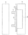
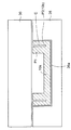
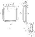
図5〜図14は実施形態の放熱板の製造方法を説明するための図、図15〜図20は実施形態の放熱板を説明するための図、図21及び図22は実施形態の電子部品装置を示す図である。以下、放熱板の製造方法を説明しながら、放熱板及び半導体装置の構造について説明する。
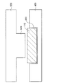
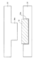
これにより、図20に示すように、外延部10bが下型28の凹部28aの開口端に接した部分で上側に曲げ加工される。このようにして、外延部10bを第1突出部P1の突出方向と逆方向に曲げることより、第1突出部P1の反対側に第2突出部P2xを形成する。
Claims (10)
- 平板部と、
前記平板部の外周部に形成され、前記平板部の厚み方向に突出する環状の第1突出部と、
前記第1突出部の外側に形成された外延部と、
前記外延部に形成され、前記第1突出部と同じ方向又は逆方向のいずれかに突出する第2突出部と
を有し、
前記第1突出部は外周が四角形状であり、
前記第1突出部の四隅の外側領域に前記第2突出部の開口部が設けられており、
前記外延部の厚みは、前記平板部の厚みよりも薄いことを特徴とする放熱板。 - 前記第2突出部は、前記第1突出部と同じ方向に突出しており、
前記第1突出部と前記第2突出部との間に隙間が設けられていることを特徴とする請求項1に記載の放熱板。 - 前記第2突出部は、前記第1突出部と同じ方向に突出しており、
前記第1突出部の先端面と前記第2突出部の先端面とは同じ高さ位置に配置されていることを特徴とする請求項1又は2に記載の放熱板。 - 前記第2突出部の厚みは、前記第1突出部の厚みよりも薄いことを特徴とする請求項1乃至3のいずれか1項に記載の放熱板。
- 配線基板と、
前記配線基板の上に搭載された電子部品と、
請求項1乃至4のいずれか1項に記載の放熱板と
を有し、
前記放熱板の第1突出部が前記配線基板の上に配置されて、前記放熱板の中に前記電子部品が収容され、
前記放熱板と前記電子部品とが熱伝導材で接続されていることを特徴とする電子部品装置。 - 金属板を用意する工程と、
金型によって前記金属板を押圧することにより、平板部と、前記平板部の外周部に上側に突出して配置された第1突出部と、第1突出部の上部側面から外側に延びる外延部とを形成する工程と、
金型によって前記外延部を下側に押し込んで移動させることにより、前記外延部を前記第1突出部の下部側面に繋げる工程と、
前記外延部を前記第1突出部の突出方向と同じ方向又は逆方向のいずれかに曲げることにより、前記第1突出部の外側に第2突出部を形成する工程と
を有することを特徴とする放熱板の製造方法。 - 前記第2突出部を形成する工程において、
前記外延部を前記第1突出部の突出方向と同じ方向に曲げて前記第2突出部を形成し、
前記第1突出部と前記第2突出部との間に隙間が設けられることを特徴とする請求項6に記載の放熱板の製造方法。 - 前記平板部と前記第1突出部と前記外延部とを形成する工程において、
前記第1突出部の外周は四角形状で形成され、
前記外延部を前記第1突出部の下部側面に繋げる工程の後であって、前記第2突出部を形成する工程の前に、
前記外延部の先端部を除去すると共に、前記第1突出部の四隅の外側領域の前記外延部を除去して開口部を設ける工程を有することを特徴とする請求項6又は7に記載の放熱板の製造方法。 - 前記平板部と前記第1突出部と前記外延部とを形成する工程において、
前記外延部の厚みは前記平板部の厚みよりも薄く設定されることを特徴とする請求項6乃至8のいずれか一項に記載の放熱板の製造方法。 - 前記第2突出部を形成する工程において、
前記外延部を前記第1突出部の突出方向と同じ方向に曲げて前記第2突出部を形成し、
前記第1突出部の先端面と前記第2突出部の先端面とが同じ高さ位置に配置されることを特徴とする請求項6乃至9のいずれか一項に記載の放熱板の製造方法。
Priority Applications (2)
| Application Number | Priority Date | Filing Date | Title |
|---|---|---|---|
| JP2017123920A JP6867243B2 (ja) | 2017-06-26 | 2017-06-26 | 放熱板及びその製造方法と電子部品装置 |
| US15/987,390 US10461013B2 (en) | 2017-06-26 | 2018-05-23 | Heat sink and electronic component device |
Applications Claiming Priority (1)
| Application Number | Priority Date | Filing Date | Title |
|---|---|---|---|
| JP2017123920A JP6867243B2 (ja) | 2017-06-26 | 2017-06-26 | 放熱板及びその製造方法と電子部品装置 |
Publications (3)
| Publication Number | Publication Date |
|---|---|
| JP2019009292A JP2019009292A (ja) | 2019-01-17 |
| JP2019009292A5 JP2019009292A5 (ja) | 2020-02-27 |
| JP6867243B2 true JP6867243B2 (ja) | 2021-04-28 |
Family
ID=64692745
Family Applications (1)
| Application Number | Title | Priority Date | Filing Date |
|---|---|---|---|
| JP2017123920A Active JP6867243B2 (ja) | 2017-06-26 | 2017-06-26 | 放熱板及びその製造方法と電子部品装置 |
Country Status (2)
| Country | Link |
|---|---|
| US (1) | US10461013B2 (ja) |
| JP (1) | JP6867243B2 (ja) |
Families Citing this family (3)
| Publication number | Priority date | Publication date | Assignee | Title |
|---|---|---|---|---|
| US10510595B2 (en) | 2018-04-30 | 2019-12-17 | Taiwan Semiconductor Manufacturing Company, Ltd. | Integrated fan-out packages and methods of forming the same |
| US20210035921A1 (en) | 2019-07-30 | 2021-02-04 | Intel Corporation | Soldered metallic reservoirs for enhanced transient and steady-state thermal performance |
| JP2023183142A (ja) * | 2022-06-15 | 2023-12-27 | キオクシア株式会社 | 半導体装置および半導体装置の製造方法 |
Family Cites Families (17)
| Publication number | Priority date | Publication date | Assignee | Title |
|---|---|---|---|---|
| US5151777A (en) * | 1989-03-03 | 1992-09-29 | Delco Electronics Corporation | Interface device for thermally coupling an integrated circuit to a heat sink |
| JPH0531248A (ja) | 1991-08-02 | 1993-02-09 | Sophia Co Ltd | 遊技機 |
| JPH0531248U (ja) * | 1991-09-30 | 1993-04-23 | シヤープ株式会社 | 樹脂封止型電力半導体装置 |
| JP3313009B2 (ja) | 1995-05-19 | 2002-08-12 | 新光電気工業株式会社 | 放熱部材、リードフレーム及び半導体装置 |
| JPH11112169A (ja) | 1997-10-06 | 1999-04-23 | Nippon Light Metal Co Ltd | 集積回路モジュール用放熱板及びその製造方法 |
| JP2001338999A (ja) * | 2000-05-30 | 2001-12-07 | Kyocera Corp | 半導体素子収納用パッケージ |
| US20030131476A1 (en) * | 2001-09-28 | 2003-07-17 | Vlad Ocher | Heat conduits and terminal radiator for microcircuit packaging and manufacturing process |
| JP2003277853A (ja) * | 2002-03-26 | 2003-10-02 | Dowa Mining Co Ltd | ヒートスプレッダ用銅合金 |
| JP2005012127A (ja) * | 2003-06-20 | 2005-01-13 | Denso Corp | 電子制御装置 |
| JP4910439B2 (ja) * | 2006-03-23 | 2012-04-04 | 富士通セミコンダクター株式会社 | 半導体装置 |
| JP5733893B2 (ja) * | 2009-12-22 | 2015-06-10 | 新光電気工業株式会社 | 電子部品装置 |
| JP5368377B2 (ja) * | 2010-06-02 | 2013-12-18 | 三菱電機株式会社 | 電子部品パッケージおよびその製造方法 |
| JP5719566B2 (ja) | 2010-11-04 | 2015-05-20 | 新光電気工業株式会社 | Icパッケージ用放熱板及び放熱板を有するicパッケージの接続装置 |
| JP5898919B2 (ja) * | 2011-10-31 | 2016-04-06 | 新光電気工業株式会社 | 半導体装置 |
| JP6007535B2 (ja) * | 2012-03-22 | 2016-10-12 | 日本電気株式会社 | 中空封止構造及びそれを備えた中空パッケージ |
| US9524917B2 (en) * | 2014-04-23 | 2016-12-20 | Optiz, Inc. | Chip level heat dissipation using silicon |
| JP6421050B2 (ja) * | 2015-02-09 | 2018-11-07 | 株式会社ジェイデバイス | 半導体装置 |
-
2017
- 2017-06-26 JP JP2017123920A patent/JP6867243B2/ja active Active
-
2018
- 2018-05-23 US US15/987,390 patent/US10461013B2/en active Active
Also Published As
| Publication number | Publication date |
|---|---|
| US20180374773A1 (en) | 2018-12-27 |
| JP2019009292A (ja) | 2019-01-17 |
| US10461013B2 (en) | 2019-10-29 |
Similar Documents
| Publication | Publication Date | Title |
|---|---|---|
| TWI614851B (zh) | 包括多層加強件之電子封裝體 | |
| CN110024119B (zh) | 半导体装置及其制造方法 | |
| JP5899768B2 (ja) | 半導体パッケージ、配線基板ユニット、及び電子機器 | |
| CN101547586B (zh) | 散热装置、散热装置组合及其固定装置 | |
| JP6867243B2 (ja) | 放熱板及びその製造方法と電子部品装置 | |
| CN101621905A (zh) | 散热器扣具及使用该扣具的散热装置 | |
| US8553417B2 (en) | Heat-radiating substrate and method of manufacturing the same | |
| CN101547584B (zh) | 散热装置、散热装置组合及其固定装置 | |
| US10325829B2 (en) | TIM strain mitigation in electronic modules | |
| US20090135552A1 (en) | Heat dissipating device and heat sink fastener | |
| CN204217301U (zh) | 散热构造以及具备该散热构造的电子设备 | |
| US8269343B2 (en) | Semiconductor device including a pressure-contact section | |
| JP2019009292A5 (ja) | ||
| KR101089649B1 (ko) | 금속적층판 및 이를 이용한 코어기판 제조방법 | |
| JP6734594B2 (ja) | ヒートシンク及び該ヒートシンクの製造方法並びに該ヒートシンクを用いた電子部品パッケージ | |
| KR100730626B1 (ko) | 반도체 발광 장치를 위한 기판 제조 방법 | |
| US9138840B2 (en) | Method for manufacturing a heat sink | |
| JP7152544B2 (ja) | 半導体放熱パッケージ構造 | |
| JP7386435B2 (ja) | 配線基板および、その製造方法 | |
| JP5256177B2 (ja) | 半導体パッケージ | |
| CN104271693B (zh) | 导热片 | |
| CN105458100A (zh) | 散热铝盒与散热件的结合方法 | |
| CN100403526C (zh) | 半导体器件的散热结构和半导体封装 | |
| JP5882132B2 (ja) | フレキシブル回路基板及びその製造方法 | |
| CN110634806A (zh) | 半导体装置组合件和其制造方法 |
Legal Events
| Date | Code | Title | Description |
|---|---|---|---|
| RD03 | Notification of appointment of power of attorney |
Free format text: JAPANESE INTERMEDIATE CODE: A7423 Effective date: 20180320 |
|
| A521 | Request for written amendment filed |
Free format text: JAPANESE INTERMEDIATE CODE: A523 Effective date: 20200110 |
|
| A621 | Written request for application examination |
Free format text: JAPANESE INTERMEDIATE CODE: A621 Effective date: 20200110 |
|
| A131 | Notification of reasons for refusal |
Free format text: JAPANESE INTERMEDIATE CODE: A131 Effective date: 20201124 |
|
| A977 | Report on retrieval |
Free format text: JAPANESE INTERMEDIATE CODE: A971007 Effective date: 20201126 |
|
| A521 | Request for written amendment filed |
Free format text: JAPANESE INTERMEDIATE CODE: A523 Effective date: 20210114 |
|
| TRDD | Decision of grant or rejection written | ||
| A01 | Written decision to grant a patent or to grant a registration (utility model) |
Free format text: JAPANESE INTERMEDIATE CODE: A01 Effective date: 20210323 |
|
| A61 | First payment of annual fees (during grant procedure) |
Free format text: JAPANESE INTERMEDIATE CODE: A61 Effective date: 20210408 |
|
| R150 | Certificate of patent or registration of utility model |
Ref document number: 6867243 Country of ref document: JP Free format text: JAPANESE INTERMEDIATE CODE: R150 |