JP6138611B2 - 表示装置の作製方法 - Google Patents
表示装置の作製方法 Download PDFInfo
- Publication number
- JP6138611B2 JP6138611B2 JP2013145991A JP2013145991A JP6138611B2 JP 6138611 B2 JP6138611 B2 JP 6138611B2 JP 2013145991 A JP2013145991 A JP 2013145991A JP 2013145991 A JP2013145991 A JP 2013145991A JP 6138611 B2 JP6138611 B2 JP 6138611B2
- Authority
- JP
- Japan
- Prior art keywords
- substrate
- layer
- support substrate
- display device
- light
- Prior art date
- Legal status (The legal status is an assumption and is not a legal conclusion. Google has not performed a legal analysis and makes no representation as to the accuracy of the status listed.)
- Expired - Fee Related
Links
Images


Classifications
-
- G—PHYSICS
- G06—COMPUTING OR CALCULATING; COUNTING
- G06F—ELECTRIC DIGITAL DATA PROCESSING
- G06F3/00—Input arrangements for transferring data to be processed into a form capable of being handled by the computer; Output arrangements for transferring data from processing unit to output unit, e.g. interface arrangements
- G06F3/01—Input arrangements or combined input and output arrangements for interaction between user and computer
- G06F3/03—Arrangements for converting the position or the displacement of a member into a coded form
- G06F3/041—Digitisers, e.g. for touch screens or touch pads, characterised by the transducing means
- G06F3/0412—Digitisers structurally integrated in a display
-
- G—PHYSICS
- G02—OPTICS
- G02F—OPTICAL DEVICES OR ARRANGEMENTS FOR THE CONTROL OF LIGHT BY MODIFICATION OF THE OPTICAL PROPERTIES OF THE MEDIA OF THE ELEMENTS INVOLVED THEREIN; NON-LINEAR OPTICS; FREQUENCY-CHANGING OF LIGHT; OPTICAL LOGIC ELEMENTS; OPTICAL ANALOGUE/DIGITAL CONVERTERS
- G02F1/00—Devices or arrangements for the control of the intensity, colour, phase, polarisation or direction of light arriving from an independent light source, e.g. switching, gating or modulating; Non-linear optics
- G02F1/01—Devices or arrangements for the control of the intensity, colour, phase, polarisation or direction of light arriving from an independent light source, e.g. switching, gating or modulating; Non-linear optics for the control of the intensity, phase, polarisation or colour
- G02F1/13—Devices or arrangements for the control of the intensity, colour, phase, polarisation or direction of light arriving from an independent light source, e.g. switching, gating or modulating; Non-linear optics for the control of the intensity, phase, polarisation or colour based on liquid crystals, e.g. single liquid crystal display cells
- G02F1/133—Constructional arrangements; Operation of liquid crystal cells; Circuit arrangements
- G02F1/1333—Constructional arrangements; Manufacturing methods
- G02F1/13338—Input devices, e.g. touch panels
-
- G—PHYSICS
- G06—COMPUTING OR CALCULATING; COUNTING
- G06F—ELECTRIC DIGITAL DATA PROCESSING
- G06F3/00—Input arrangements for transferring data to be processed into a form capable of being handled by the computer; Output arrangements for transferring data from processing unit to output unit, e.g. interface arrangements
- G06F3/01—Input arrangements or combined input and output arrangements for interaction between user and computer
- G06F3/03—Arrangements for converting the position or the displacement of a member into a coded form
- G06F3/041—Digitisers, e.g. for touch screens or touch pads, characterised by the transducing means
- G06F3/044—Digitisers, e.g. for touch screens or touch pads, characterised by the transducing means by capacitive means
- G06F3/0443—Digitisers, e.g. for touch screens or touch pads, characterised by the transducing means by capacitive means using a single layer of sensing electrodes
-
- G—PHYSICS
- G06—COMPUTING OR CALCULATING; COUNTING
- G06F—ELECTRIC DIGITAL DATA PROCESSING
- G06F3/00—Input arrangements for transferring data to be processed into a form capable of being handled by the computer; Output arrangements for transferring data from processing unit to output unit, e.g. interface arrangements
- G06F3/01—Input arrangements or combined input and output arrangements for interaction between user and computer
- G06F3/03—Arrangements for converting the position or the displacement of a member into a coded form
- G06F3/041—Digitisers, e.g. for touch screens or touch pads, characterised by the transducing means
- G06F3/044—Digitisers, e.g. for touch screens or touch pads, characterised by the transducing means by capacitive means
- G06F3/0445—Digitisers, e.g. for touch screens or touch pads, characterised by the transducing means by capacitive means using two or more layers of sensing electrodes, e.g. using two layers of electrodes separated by a dielectric layer
-
- G—PHYSICS
- G09—EDUCATION; CRYPTOGRAPHY; DISPLAY; ADVERTISING; SEALS
- G09F—DISPLAYING; ADVERTISING; SIGNS; LABELS OR NAME-PLATES; SEALS
- G09F9/00—Indicating arrangements for variable information in which the information is built-up on a support by selection or combination of individual elements
- G09F9/30—Indicating arrangements for variable information in which the information is built-up on a support by selection or combination of individual elements in which the desired character or characters are formed by combining individual elements
- G09F9/301—Indicating arrangements for variable information in which the information is built-up on a support by selection or combination of individual elements in which the desired character or characters are formed by combining individual elements flexible foldable or roll-able electronic displays, e.g. thin LCD, OLED
-
- H—ELECTRICITY
- H10—SEMICONDUCTOR DEVICES; ELECTRIC SOLID-STATE DEVICES NOT OTHERWISE PROVIDED FOR
- H10D—INORGANIC ELECTRIC SEMICONDUCTOR DEVICES
- H10D30/00—Field-effect transistors [FET]
- H10D30/60—Insulated-gate field-effect transistors [IGFET]
- H10D30/67—Thin-film transistors [TFT]
- H10D30/674—Thin-film transistors [TFT] characterised by the active materials
- H10D30/6755—Oxide semiconductors, e.g. zinc oxide, copper aluminium oxide or cadmium stannate
-
- H—ELECTRICITY
- H10—SEMICONDUCTOR DEVICES; ELECTRIC SOLID-STATE DEVICES NOT OTHERWISE PROVIDED FOR
- H10D—INORGANIC ELECTRIC SEMICONDUCTOR DEVICES
- H10D84/00—Integrated devices formed in or on semiconductor substrates that comprise only semiconducting layers, e.g. on Si wafers or on GaAs-on-Si wafers
- H10D84/01—Manufacture or treatment
-
- H—ELECTRICITY
- H10—SEMICONDUCTOR DEVICES; ELECTRIC SOLID-STATE DEVICES NOT OTHERWISE PROVIDED FOR
- H10D—INORGANIC ELECTRIC SEMICONDUCTOR DEVICES
- H10D86/00—Integrated devices formed in or on insulating or conducting substrates, e.g. formed in silicon-on-insulator [SOI] substrates or on stainless steel or glass substrates
- H10D86/40—Integrated devices formed in or on insulating or conducting substrates, e.g. formed in silicon-on-insulator [SOI] substrates or on stainless steel or glass substrates characterised by multiple TFTs
- H10D86/411—Integrated devices formed in or on insulating or conducting substrates, e.g. formed in silicon-on-insulator [SOI] substrates or on stainless steel or glass substrates characterised by multiple TFTs characterised by materials, geometry or structure of the substrates
-
- H—ELECTRICITY
- H10—SEMICONDUCTOR DEVICES; ELECTRIC SOLID-STATE DEVICES NOT OTHERWISE PROVIDED FOR
- H10D—INORGANIC ELECTRIC SEMICONDUCTOR DEVICES
- H10D86/00—Integrated devices formed in or on insulating or conducting substrates, e.g. formed in silicon-on-insulator [SOI] substrates or on stainless steel or glass substrates
- H10D86/40—Integrated devices formed in or on insulating or conducting substrates, e.g. formed in silicon-on-insulator [SOI] substrates or on stainless steel or glass substrates characterised by multiple TFTs
- H10D86/60—Integrated devices formed in or on insulating or conducting substrates, e.g. formed in silicon-on-insulator [SOI] substrates or on stainless steel or glass substrates characterised by multiple TFTs wherein the TFTs are in active matrices
-
- H—ELECTRICITY
- H10—SEMICONDUCTOR DEVICES; ELECTRIC SOLID-STATE DEVICES NOT OTHERWISE PROVIDED FOR
- H10H—INORGANIC LIGHT-EMITTING SEMICONDUCTOR DEVICES HAVING POTENTIAL BARRIERS
- H10H29/00—Integrated devices, or assemblies of multiple devices, comprising at least one light-emitting semiconductor element covered by group H10H20/00
- H10H29/10—Integrated devices comprising at least one light-emitting semiconductor component covered by group H10H20/00
-
- H—ELECTRICITY
- H10—SEMICONDUCTOR DEVICES; ELECTRIC SOLID-STATE DEVICES NOT OTHERWISE PROVIDED FOR
- H10K—ORGANIC ELECTRIC SOLID-STATE DEVICES
- H10K59/00—Integrated devices, or assemblies of multiple devices, comprising at least one organic light-emitting element covered by group H10K50/00
- H10K59/10—OLED displays
- H10K59/12—Active-matrix OLED [AMOLED] displays
-
- H—ELECTRICITY
- H10—SEMICONDUCTOR DEVICES; ELECTRIC SOLID-STATE DEVICES NOT OTHERWISE PROVIDED FOR
- H10K—ORGANIC ELECTRIC SOLID-STATE DEVICES
- H10K59/00—Integrated devices, or assemblies of multiple devices, comprising at least one organic light-emitting element covered by group H10K50/00
- H10K59/30—Devices specially adapted for multicolour light emission
- H10K59/38—Devices specially adapted for multicolour light emission comprising colour filters or colour changing media [CCM]
-
- H—ELECTRICITY
- H10—SEMICONDUCTOR DEVICES; ELECTRIC SOLID-STATE DEVICES NOT OTHERWISE PROVIDED FOR
- H10K—ORGANIC ELECTRIC SOLID-STATE DEVICES
- H10K59/00—Integrated devices, or assemblies of multiple devices, comprising at least one organic light-emitting element covered by group H10K50/00
- H10K59/40—OLEDs integrated with touch screens
-
- H—ELECTRICITY
- H10—SEMICONDUCTOR DEVICES; ELECTRIC SOLID-STATE DEVICES NOT OTHERWISE PROVIDED FOR
- H10K—ORGANIC ELECTRIC SOLID-STATE DEVICES
- H10K59/00—Integrated devices, or assemblies of multiple devices, comprising at least one organic light-emitting element covered by group H10K50/00
- H10K59/60—OLEDs integrated with inorganic light-sensitive elements, e.g. with inorganic solar cells or inorganic photodiodes
-
- H—ELECTRICITY
- H10—SEMICONDUCTOR DEVICES; ELECTRIC SOLID-STATE DEVICES NOT OTHERWISE PROVIDED FOR
- H10K—ORGANIC ELECTRIC SOLID-STATE DEVICES
- H10K59/00—Integrated devices, or assemblies of multiple devices, comprising at least one organic light-emitting element covered by group H10K50/00
- H10K59/80—Constructional details
- H10K59/87—Passivation; Containers; Encapsulations
- H10K59/871—Self-supporting sealing arrangements
- H10K59/8722—Peripheral sealing arrangements, e.g. adhesives, sealants
-
- H—ELECTRICITY
- H10—SEMICONDUCTOR DEVICES; ELECTRIC SOLID-STATE DEVICES NOT OTHERWISE PROVIDED FOR
- H10K—ORGANIC ELECTRIC SOLID-STATE DEVICES
- H10K71/00—Manufacture or treatment specially adapted for the organic devices covered by this subclass
- H10K71/80—Manufacture or treatment specially adapted for the organic devices covered by this subclass using temporary substrates
-
- H—ELECTRICITY
- H10—SEMICONDUCTOR DEVICES; ELECTRIC SOLID-STATE DEVICES NOT OTHERWISE PROVIDED FOR
- H10K—ORGANIC ELECTRIC SOLID-STATE DEVICES
- H10K77/00—Constructional details of devices covered by this subclass and not covered by groups H10K10/80, H10K30/80, H10K50/80 or H10K59/80
- H10K77/10—Substrates, e.g. flexible substrates
- H10K77/111—Flexible substrates
-
- H—ELECTRICITY
- H10—SEMICONDUCTOR DEVICES; ELECTRIC SOLID-STATE DEVICES NOT OTHERWISE PROVIDED FOR
- H10P—GENERIC PROCESSES OR APPARATUS FOR THE MANUFACTURE OR TREATMENT OF DEVICES COVERED BY CLASS H10
- H10P72/00—Handling or holding of wafers, substrates or devices during manufacture or treatment thereof
- H10P72/70—Handling or holding of wafers, substrates or devices during manufacture or treatment thereof for supporting or gripping
- H10P72/74—Handling or holding of wafers, substrates or devices during manufacture or treatment thereof for supporting or gripping using temporarily an auxiliary support
-
- G—PHYSICS
- G02—OPTICS
- G02F—OPTICAL DEVICES OR ARRANGEMENTS FOR THE CONTROL OF LIGHT BY MODIFICATION OF THE OPTICAL PROPERTIES OF THE MEDIA OF THE ELEMENTS INVOLVED THEREIN; NON-LINEAR OPTICS; FREQUENCY-CHANGING OF LIGHT; OPTICAL LOGIC ELEMENTS; OPTICAL ANALOGUE/DIGITAL CONVERTERS
- G02F1/00—Devices or arrangements for the control of the intensity, colour, phase, polarisation or direction of light arriving from an independent light source, e.g. switching, gating or modulating; Non-linear optics
- G02F1/01—Devices or arrangements for the control of the intensity, colour, phase, polarisation or direction of light arriving from an independent light source, e.g. switching, gating or modulating; Non-linear optics for the control of the intensity, phase, polarisation or colour
- G02F1/13—Devices or arrangements for the control of the intensity, colour, phase, polarisation or direction of light arriving from an independent light source, e.g. switching, gating or modulating; Non-linear optics for the control of the intensity, phase, polarisation or colour based on liquid crystals, e.g. single liquid crystal display cells
- G02F1/133—Constructional arrangements; Operation of liquid crystal cells; Circuit arrangements
- G02F1/1333—Constructional arrangements; Manufacturing methods
- G02F1/133308—Support structures for LCD panels, e.g. frames or bezels
- G02F1/133325—Assembling processes
-
- G—PHYSICS
- G02—OPTICS
- G02F—OPTICAL DEVICES OR ARRANGEMENTS FOR THE CONTROL OF LIGHT BY MODIFICATION OF THE OPTICAL PROPERTIES OF THE MEDIA OF THE ELEMENTS INVOLVED THEREIN; NON-LINEAR OPTICS; FREQUENCY-CHANGING OF LIGHT; OPTICAL LOGIC ELEMENTS; OPTICAL ANALOGUE/DIGITAL CONVERTERS
- G02F1/00—Devices or arrangements for the control of the intensity, colour, phase, polarisation or direction of light arriving from an independent light source, e.g. switching, gating or modulating; Non-linear optics
- G02F1/01—Devices or arrangements for the control of the intensity, colour, phase, polarisation or direction of light arriving from an independent light source, e.g. switching, gating or modulating; Non-linear optics for the control of the intensity, phase, polarisation or colour
- G02F1/13—Devices or arrangements for the control of the intensity, colour, phase, polarisation or direction of light arriving from an independent light source, e.g. switching, gating or modulating; Non-linear optics for the control of the intensity, phase, polarisation or colour based on liquid crystals, e.g. single liquid crystal display cells
- G02F1/133—Constructional arrangements; Operation of liquid crystal cells; Circuit arrangements
- G02F1/136—Liquid crystal cells structurally associated with a semi-conducting layer or substrate, e.g. cells forming part of an integrated circuit
- G02F1/13606—Liquid crystal cells structurally associated with a semi-conducting layer or substrate, e.g. cells forming part of an integrated circuit having means for reducing parasitic capacitance
-
- G—PHYSICS
- G02—OPTICS
- G02F—OPTICAL DEVICES OR ARRANGEMENTS FOR THE CONTROL OF LIGHT BY MODIFICATION OF THE OPTICAL PROPERTIES OF THE MEDIA OF THE ELEMENTS INVOLVED THEREIN; NON-LINEAR OPTICS; FREQUENCY-CHANGING OF LIGHT; OPTICAL LOGIC ELEMENTS; OPTICAL ANALOGUE/DIGITAL CONVERTERS
- G02F1/00—Devices or arrangements for the control of the intensity, colour, phase, polarisation or direction of light arriving from an independent light source, e.g. switching, gating or modulating; Non-linear optics
- G02F1/01—Devices or arrangements for the control of the intensity, colour, phase, polarisation or direction of light arriving from an independent light source, e.g. switching, gating or modulating; Non-linear optics for the control of the intensity, phase, polarisation or colour
- G02F1/13—Devices or arrangements for the control of the intensity, colour, phase, polarisation or direction of light arriving from an independent light source, e.g. switching, gating or modulating; Non-linear optics for the control of the intensity, phase, polarisation or colour based on liquid crystals, e.g. single liquid crystal display cells
- G02F1/133—Constructional arrangements; Operation of liquid crystal cells; Circuit arrangements
- G02F1/136—Liquid crystal cells structurally associated with a semi-conducting layer or substrate, e.g. cells forming part of an integrated circuit
- G02F1/1362—Active matrix addressed cells
- G02F1/1368—Active matrix addressed cells in which the switching element is a three-electrode device
-
- G—PHYSICS
- G02—OPTICS
- G02F—OPTICAL DEVICES OR ARRANGEMENTS FOR THE CONTROL OF LIGHT BY MODIFICATION OF THE OPTICAL PROPERTIES OF THE MEDIA OF THE ELEMENTS INVOLVED THEREIN; NON-LINEAR OPTICS; FREQUENCY-CHANGING OF LIGHT; OPTICAL LOGIC ELEMENTS; OPTICAL ANALOGUE/DIGITAL CONVERTERS
- G02F2202/00—Materials and properties
- G02F2202/28—Adhesive materials or arrangements
-
- G—PHYSICS
- G06—COMPUTING OR CALCULATING; COUNTING
- G06F—ELECTRIC DIGITAL DATA PROCESSING
- G06F2203/00—Indexing scheme relating to G06F3/00 - G06F3/048
- G06F2203/041—Indexing scheme relating to G06F3/041 - G06F3/045
- G06F2203/04103—Manufacturing, i.e. details related to manufacturing processes specially suited for touch sensitive devices
-
- H—ELECTRICITY
- H10—SEMICONDUCTOR DEVICES; ELECTRIC SOLID-STATE DEVICES NOT OTHERWISE PROVIDED FOR
- H10D—INORGANIC ELECTRIC SEMICONDUCTOR DEVICES
- H10D86/00—Integrated devices formed in or on insulating or conducting substrates, e.g. formed in silicon-on-insulator [SOI] substrates or on stainless steel or glass substrates
- H10D86/40—Integrated devices formed in or on insulating or conducting substrates, e.g. formed in silicon-on-insulator [SOI] substrates or on stainless steel or glass substrates characterised by multiple TFTs
- H10D86/421—Integrated devices formed in or on insulating or conducting substrates, e.g. formed in silicon-on-insulator [SOI] substrates or on stainless steel or glass substrates characterised by multiple TFTs having a particular composition, shape or crystalline structure of the active layer
- H10D86/423—Integrated devices formed in or on insulating or conducting substrates, e.g. formed in silicon-on-insulator [SOI] substrates or on stainless steel or glass substrates characterised by multiple TFTs having a particular composition, shape or crystalline structure of the active layer comprising semiconductor materials not belonging to the Group IV, e.g. InGaZnO
-
- H—ELECTRICITY
- H10—SEMICONDUCTOR DEVICES; ELECTRIC SOLID-STATE DEVICES NOT OTHERWISE PROVIDED FOR
- H10K—ORGANIC ELECTRIC SOLID-STATE DEVICES
- H10K2102/00—Constructional details relating to the organic devices covered by this subclass
- H10K2102/301—Details of OLEDs
- H10K2102/311—Flexible OLED
-
- H—ELECTRICITY
- H10—SEMICONDUCTOR DEVICES; ELECTRIC SOLID-STATE DEVICES NOT OTHERWISE PROVIDED FOR
- H10K—ORGANIC ELECTRIC SOLID-STATE DEVICES
- H10K2102/00—Constructional details relating to the organic devices covered by this subclass
- H10K2102/301—Details of OLEDs
- H10K2102/351—Thickness
-
- H—ELECTRICITY
- H10—SEMICONDUCTOR DEVICES; ELECTRIC SOLID-STATE DEVICES NOT OTHERWISE PROVIDED FOR
- H10P—GENERIC PROCESSES OR APPARATUS FOR THE MANUFACTURE OR TREATMENT OF DEVICES COVERED BY CLASS H10
- H10P72/00—Handling or holding of wafers, substrates or devices during manufacture or treatment thereof
- H10P72/70—Handling or holding of wafers, substrates or devices during manufacture or treatment thereof for supporting or gripping
- H10P72/74—Handling or holding of wafers, substrates or devices during manufacture or treatment thereof for supporting or gripping using temporarily an auxiliary support
- H10P72/7432—Handling or holding of wafers, substrates or devices during manufacture or treatment thereof for supporting or gripping using temporarily an auxiliary support used in a transfer process involving transfer directly from an origin substrate to a target substrate without use of an intermediate handle substrate
-
- H—ELECTRICITY
- H10—SEMICONDUCTOR DEVICES; ELECTRIC SOLID-STATE DEVICES NOT OTHERWISE PROVIDED FOR
- H10P—GENERIC PROCESSES OR APPARATUS FOR THE MANUFACTURE OR TREATMENT OF DEVICES COVERED BY CLASS H10
- H10P72/00—Handling or holding of wafers, substrates or devices during manufacture or treatment thereof
- H10P72/70—Handling or holding of wafers, substrates or devices during manufacture or treatment thereof for supporting or gripping
- H10P72/74—Handling or holding of wafers, substrates or devices during manufacture or treatment thereof for supporting or gripping using temporarily an auxiliary support
- H10P72/744—Details of chemical or physical process used for separating the auxiliary support from a device or a wafer
- H10P72/7442—Separation by peeling
Landscapes
- Engineering & Computer Science (AREA)
- Theoretical Computer Science (AREA)
- General Engineering & Computer Science (AREA)
- Physics & Mathematics (AREA)
- General Physics & Mathematics (AREA)
- Human Computer Interaction (AREA)
- Nonlinear Science (AREA)
- Chemical & Material Sciences (AREA)
- Manufacturing & Machinery (AREA)
- Microelectronics & Electronic Packaging (AREA)
- Optics & Photonics (AREA)
- Crystallography & Structural Chemistry (AREA)
- Mathematical Physics (AREA)
- Life Sciences & Earth Sciences (AREA)
- Inorganic Chemistry (AREA)
- Sustainable Development (AREA)
- Devices For Indicating Variable Information By Combining Individual Elements (AREA)
- Electroluminescent Light Sources (AREA)
- Display Devices Of Pinball Game Machines (AREA)
- Led Device Packages (AREA)
Description
本実施の形態では、本発明の一態様の表示装置の構成例及びその作製方法例について、図面を参照して説明する。
まず、第1の支持基板102上に第1の基板101が積層された積層基板を準備する。
以下では、上記作製方法例1とは異なる表示装置の作製方法例について説明する。具体的には、カラーフィルタを備える表示装置について説明する。なおここでは作製方法例1と重複する部分については説明を省略するか簡略化して説明する。
以下では、上記作製方法例2とは一部が異なる表示装置の作製方法について説明する。なおここでは上記と重複する部分については説明を省略するか簡略化して説明する。
本作製方法例では上記作製方法例とは異なる表示装置の作製方法例について説明する。
本実施の形態では、実施の形態1で例示した表示装置の作製方法により作製可能な表示装置について、より具体的な構成例を例示する。なお以下では、実施の形態1と重複する部分については、説明を省略するか簡略化して説明する。
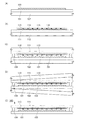
図5(A)は本構成例で例示する表示装置200の斜視概略図である。なお図5には明瞭化のため、代表的な構成要素のみを示している。
以下では、表示部201に有機EL素子が適用された表示装置200の断面構成例について説明する。
以下では、表示部201に液晶素子が適用された表示装置200の断面構成例について説明する。なお、上記と重複する部分については説明を省略するか、簡略化して説明する。
本実施の形態では、本発明の一態様の発光装置に適用可能な発光素子の構成例について、図面を参照して説明する。
発光素子の構成の一例を図8(A)に示す。図8(A)に示す発光素子は、陽極1101と陰極1102の間に発光ユニット1103を含むEL層が挟まれている。
発光素子の構成の他の一例を図8(C)に示す。図8(C)に例示する発光素子は、陽極1101と陰極1102の間に発光ユニット1103を含むEL層が挟まれている。さらに、陰極1102と発光ユニット1103との間には中間層1104が設けられている。なお、当該発光素子の構成例2の発光ユニット1103には、上述の発光素子の構成例1が備える発光ユニットと同様の構成が適用可能であり、詳細については、発光素子の構成例1の記載を参酌できる。
発光素子の構成の他の一例を図8(D)に示す。図8(D)に例示する発光素子は、陽極1101と陰極1102の間に2つの発光ユニットが設けられたEL層を備えている。さらに、第1の発光ユニット1103aと、第2の発光ユニット1103bとの間には中間層1104が設けられている。
上記実施の形態で例示したトランジスタのチャネルが形成される領域に好適に用いることができる半導体の一例について、以下に説明する。
本実施の形態では、本発明の一態様であるタッチセンサを備える表示装置を備える電子機器の例について、図9を参照して説明する。
101 基板
102 支持基板
103 素子層
104 接着層
105 接着層
110 表示装置
111 基板
112 支持基板
113 センサ層
114 センサ電極
115 センサ電極
116 絶縁層
120 表示装置
121 基板
122 支持基板
123 カラーフィルタ層
124 赤色カラーフィルタ
125 緑色カラーフィルタ
126 青色カラーフィルタ
127 ブラックマトリクス
128 絶縁層
130 表示装置
200 表示装置
201 表示部
202 タッチセンサ
203 コンタクト部
204 FPC
205 外部接続電極
206 配線
207 配線
208 接続層
209 補強材
211 画素部
212 ソース駆動回路
213 ゲート駆動回路
220 発光素子
221 電極層
222 EL層
223 電極層
231 トランジスタ
232 トランジスタ
233 トランジスタ
234 トランジスタ
235 絶縁層
236 スペーサ
237 絶縁層
238 絶縁層
239 絶縁層
241 絶縁層
242 ブラックマトリクス
243 カラーフィルタ
244 電極
245 導電性粒子
246 樹脂層
250 液晶素子
251 電極層
252 液晶
253 電極層
254 スペーサ
255 オーバーコート
256 トランジスタ
1011 筐体
1012 パネル
1013 ボタン
1014 スピーカー
1021a 筐体
1021b 筐体
1022a パネル
1022b パネル
1023 軸部
1024 ボタン
1025 接続端子
1026 記録媒体挿入部
1027 スピーカー
1031 筐体
1032 パネル
1033 ボタン
1034 スピーカー
1035 甲板部
1041 筐体
1042 パネル
1043 支持台
1044 ボタン
1045 接続端子
1046 スピーカー
1101 陽極
1102 陰極
1103 発光ユニット
1103a 発光ユニット
1103b 発光ユニット
1104 中間層
1104a 電子注入バッファー
1104b 電子リレー層
1104c 電荷発生領域
1113 正孔注入層
1114 正孔輸送層
1115 発光層
1116 電子輸送層
1117 電子注入層
Claims (4)
- 第1の支持基板上に固定され、該第1の支持基板と対向しない面上に発光素子を備える素子層が設けられた第1の基板と、第3の支持基板上に固定され、該第3の支持基板と対向しない面上にカラーフィルタ層を備える第3の基板とを、前記素子層と前記カラーフィルタ層が対向するように、第1の接着層により接着した後に、前記第3の基板と前記第3の支持基板との間で前記第3の支持基板を剥離する工程と、
前記第3の基板と、第2の支持基板上に固定され、該第2の支持基板と対向しない面上にセンサ層が設けられた第2の基板とを、前記素子層と前記センサ層が対向するように、第2の接着層により接着した後に、前記第2の基板と前記第2の支持基板との間で前記第2の支持基板を剥離する工程と、前記第1の基板と前記第1の支持基板との間で前記第1の支持基板を剥離する工程と、を有し、
前記第1の基板、前記第2の基板、及び前記第3の基板に、厚さが10μm以上200μm以下であるガラス基板を用い、
前記第1の支持基板、前記第2の支持基板、及び前記第3の支持基板に、前記ガラス基板よりも厚い基材を用いることを特徴とする表示装置の作製方法。 - 第1の支持基板上に固定され、該第1の支持基板と対向しない面上に発光素子を備える素子層が設けられた第1の基板と、第3の支持基板上に固定され、該第3の支持基板と対向しない面上にカラーフィルタ層を備える第3の基板とを、前記素子層と前記カラーフィルタ層が対向するように、第1の接着層により接着した後に、前記第1の基板と前記第1の支持基板との間で前記第1の支持基板を剥離する工程と、
前記第1の基板と、第2の支持基板上に固定され、該第2の支持基板と対向しない面上にセンサ層が設けられた第2の基板とを、前記カラーフィルタ層と前記センサ層が対向するように、第2の接着層により接着した後に、前記第2の基板と前記第2の支持基板との間で前記第2の支持基板を剥離する工程と、前記第3の基板と前記第3の支持基板との間で前記第3の支持基板を剥離する工程と、を有し、
前記第1の基板、前記第2の基板、及び前記第3の基板に、厚さが10μm以上200μm以下であるガラス基板を用い、
前記第1の支持基板、前記第2の支持基板、及び前記第3の支持基板に、前記ガラス基板よりも厚い基材を用いることを特徴とする表示装置の作製方法。 - 請求項1または請求項2において、
前記ガラス基板が前記基材と密着することにより固定され、
前記ガラス基板と前記基材の各々は、密着面における表面粗さが2nm以下であることを特徴とする表示装置の作製方法。 - 請求項1または請求項2において、
前記基材上に有機化合物または珪素化合物を含む樹脂を備え、
前記樹脂と前記ガラス基板が密着することにより、前記ガラス基板が前記基材に固定されていることを特徴とする表示装置の作製方法。
Priority Applications (1)
| Application Number | Priority Date | Filing Date | Title |
|---|---|---|---|
| JP2013145991A JP6138611B2 (ja) | 2012-07-12 | 2013-07-12 | 表示装置の作製方法 |
Applications Claiming Priority (3)
| Application Number | Priority Date | Filing Date | Title |
|---|---|---|---|
| JP2012156357 | 2012-07-12 | ||
| JP2012156357 | 2012-07-12 | ||
| JP2013145991A JP6138611B2 (ja) | 2012-07-12 | 2013-07-12 | 表示装置の作製方法 |
Related Child Applications (1)
| Application Number | Title | Priority Date | Filing Date |
|---|---|---|---|
| JP2017086824A Division JP6460603B2 (ja) | 2012-07-12 | 2017-04-26 | 表示装置の作製方法 |
Publications (3)
| Publication Number | Publication Date |
|---|---|
| JP2014032960A JP2014032960A (ja) | 2014-02-20 |
| JP2014032960A5 JP2014032960A5 (ja) | 2016-07-28 |
| JP6138611B2 true JP6138611B2 (ja) | 2017-05-31 |
Family
ID=49781683
Family Applications (7)
| Application Number | Title | Priority Date | Filing Date |
|---|---|---|---|
| JP2013145991A Expired - Fee Related JP6138611B2 (ja) | 2012-07-12 | 2013-07-12 | 表示装置の作製方法 |
| JP2017086824A Active JP6460603B2 (ja) | 2012-07-12 | 2017-04-26 | 表示装置の作製方法 |
| JP2018240427A Withdrawn JP2019091046A (ja) | 2012-07-12 | 2018-12-24 | 表示装置 |
| JP2020103576A Withdrawn JP2020160469A (ja) | 2012-07-12 | 2020-06-16 | 表示装置 |
| JP2020211269A Withdrawn JP2021044267A (ja) | 2012-07-12 | 2020-12-21 | 電子機器 |
| JP2023133547A Withdrawn JP2023157960A (ja) | 2012-07-12 | 2023-08-18 | 表示装置 |
| JP2025078486A Pending JP2025114745A (ja) | 2012-07-12 | 2025-05-09 | 表示装置の作製方法 |
Family Applications After (6)
| Application Number | Title | Priority Date | Filing Date |
|---|---|---|---|
| JP2017086824A Active JP6460603B2 (ja) | 2012-07-12 | 2017-04-26 | 表示装置の作製方法 |
| JP2018240427A Withdrawn JP2019091046A (ja) | 2012-07-12 | 2018-12-24 | 表示装置 |
| JP2020103576A Withdrawn JP2020160469A (ja) | 2012-07-12 | 2020-06-16 | 表示装置 |
| JP2020211269A Withdrawn JP2021044267A (ja) | 2012-07-12 | 2020-12-21 | 電子機器 |
| JP2023133547A Withdrawn JP2023157960A (ja) | 2012-07-12 | 2023-08-18 | 表示装置 |
| JP2025078486A Pending JP2025114745A (ja) | 2012-07-12 | 2025-05-09 | 表示装置の作製方法 |
Country Status (5)
| Country | Link |
|---|---|
| US (9) | US9082678B2 (ja) |
| JP (7) | JP6138611B2 (ja) |
| KR (6) | KR102173801B1 (ja) |
| DE (1) | DE102013213552A1 (ja) |
| TW (3) | TWI601998B (ja) |
Families Citing this family (106)
| Publication number | Priority date | Publication date | Assignee | Title |
|---|---|---|---|---|
| TWI669835B (zh) | 2012-07-05 | 2019-08-21 | 日商半導體能源研究所股份有限公司 | 發光裝置 |
| KR102114212B1 (ko) | 2012-08-10 | 2020-05-22 | 가부시키가이샤 한도오따이 에네루기 켄큐쇼 | 표시 장치 |
| US11074025B2 (en) * | 2012-09-03 | 2021-07-27 | Semiconductor Energy Laboratory Co., Ltd. | Display device and method for manufacturing the same |
| KR102245511B1 (ko) * | 2012-12-27 | 2021-04-28 | 엘지디스플레이 주식회사 | 플렉서블 유기 발광 표시 장치 및 플렉서블 유기 발광 표시 장치 제조 방법 |
| KR20140090853A (ko) * | 2013-01-10 | 2014-07-18 | 삼성디스플레이 주식회사 | 표시 장치 |
| US20160109751A1 (en) * | 2013-07-17 | 2016-04-21 | Sakai Display Products Corporation | Color Filter, Liquid Crystal Display Apparatus, and Method of Manufacturing Color Filter |
| JP6253923B2 (ja) * | 2013-08-30 | 2017-12-27 | 株式会社ジャパンディスプレイ | タッチセンサ内蔵有機エレクトロルミネッセンス装置 |
| JP6200738B2 (ja) * | 2013-09-19 | 2017-09-20 | 株式会社ジャパンディスプレイ | 表示装置及びその製造方法 |
| KR102145389B1 (ko) * | 2013-10-21 | 2020-08-19 | 삼성디스플레이 주식회사 | 표시 장치 |
| KR102239367B1 (ko) | 2013-11-27 | 2021-04-09 | 가부시키가이샤 한도오따이 에네루기 켄큐쇼 | 터치 패널 |
| KR20150086763A (ko) * | 2014-01-20 | 2015-07-29 | 삼성디스플레이 주식회사 | 발광형 표시장치 및 그 제조방법 |
| CN103886813B (zh) * | 2014-02-14 | 2016-07-06 | 上海和辉光电有限公司 | 双面显示器、双面显示器的控制装置及其制造方法 |
| JP6484846B2 (ja) * | 2014-03-11 | 2019-03-20 | 大日本印刷株式会社 | タッチパネル、表示装置及び光学シート、並びに光学シートの選別方法及び光学シートの製造方法 |
| TWI764064B (zh) * | 2014-03-13 | 2022-05-11 | 日商半導體能源研究所股份有限公司 | 撓性裝置 |
| TWI831924B (zh) * | 2014-04-25 | 2024-02-11 | 日商半導體能源研究所股份有限公司 | 顯示裝置及電子裝置 |
| JP2015228367A (ja) | 2014-05-02 | 2015-12-17 | 株式会社半導体エネルギー研究所 | 半導体装置、入出力装置、及び電子機器 |
| US10073571B2 (en) | 2014-05-02 | 2018-09-11 | Semiconductor Energy Laboratory Co., Ltd. | Touch sensor and touch panel including capacitor |
| JP6722980B2 (ja) * | 2014-05-09 | 2020-07-15 | 株式会社半導体エネルギー研究所 | 表示装置および発光装置、並びに電子機器 |
| TWI790965B (zh) * | 2014-05-30 | 2023-01-21 | 日商半導體能源研究所股份有限公司 | 觸控面板 |
| KR20250102133A (ko) | 2014-05-30 | 2025-07-04 | 가부시키가이샤 한도오따이 에네루기 켄큐쇼 | 발광 장치, 표시 장치, 및 전자 기기 |
| TWI814461B (zh) | 2014-06-18 | 2023-09-01 | 愛爾蘭商艾克斯展示公司技術有限公司 | 微組裝發光二極體顯示器及照明元件 |
| KR102245504B1 (ko) * | 2014-06-19 | 2021-04-27 | 엘지디스플레이 주식회사 | 유기 발광 표시 장치 및 유기 발광 표시 장치 제조 방법 |
| CN106463082B (zh) * | 2014-06-23 | 2019-07-16 | 株式会社半导体能源研究所 | 显示装置及电子设备 |
| JP6497858B2 (ja) * | 2014-07-11 | 2019-04-10 | 株式会社ジャパンディスプレイ | 有機el表示装置及び有機el表示装置の製造方法 |
| US10042110B2 (en) * | 2014-07-21 | 2018-08-07 | Samsung Display Co., Ltd. | Liquid crystal display and manufacturing method thereof |
| KR20160014864A (ko) * | 2014-07-29 | 2016-02-12 | 엘지디스플레이 주식회사 | 터치스크린패널 액정표시장치 |
| KR102271659B1 (ko) * | 2014-08-29 | 2021-06-30 | 엘지디스플레이 주식회사 | 터치 패널 내장형 유기 발광 표시 장치 |
| JP6612236B2 (ja) * | 2014-09-04 | 2019-11-27 | 株式会社Joled | 表示装置および電子機器 |
| KR102360783B1 (ko) * | 2014-09-16 | 2022-02-10 | 삼성디스플레이 주식회사 | 디스플레이 장치 |
| US9799719B2 (en) | 2014-09-25 | 2017-10-24 | X-Celeprint Limited | Active-matrix touchscreen |
| US9991163B2 (en) | 2014-09-25 | 2018-06-05 | X-Celeprint Limited | Small-aperture-ratio display with electrical component |
| JP2016075721A (ja) * | 2014-10-02 | 2016-05-12 | 株式会社ジャパンディスプレイ | 液晶表示装置 |
| WO2016059497A1 (en) | 2014-10-17 | 2016-04-21 | Semiconductor Energy Laboratory Co., Ltd. | Light-emitting device, module, electronic device, and method for manufacturing light-emitting device |
| KR102295584B1 (ko) * | 2014-10-31 | 2021-08-27 | 엘지디스플레이 주식회사 | 터치 패널 내장형 유기 발광 표시 장치 |
| KR102250847B1 (ko) * | 2014-11-13 | 2021-05-13 | 삼성디스플레이 주식회사 | 터치 스크린 패널 일체형 표시장치 |
| KR102326807B1 (ko) * | 2014-11-26 | 2021-11-15 | 엘지디스플레이 주식회사 | 유기발광표시장치 및 이의 제조방법 |
| KR102239861B1 (ko) | 2014-11-26 | 2021-04-13 | 삼성디스플레이 주식회사 | 터치 센서를 포함하는 표시 장치 및 그 구동 방법 |
| US9743513B2 (en) | 2014-12-26 | 2017-08-22 | Industrial Technology Research Institute | Flexible electronic device |
| TWI589194B (zh) * | 2014-12-26 | 2017-06-21 | 財團法人工業技術研究院 | 軟性電子裝置 |
| US20180011575A1 (en) * | 2015-01-21 | 2018-01-11 | Lg Innotek Co., Ltd. | Touch window |
| KR102362188B1 (ko) * | 2015-01-28 | 2022-02-11 | 삼성디스플레이 주식회사 | 유기 발광 표시 장치 및 그의 제조 방법 |
| JP2016143457A (ja) * | 2015-01-30 | 2016-08-08 | パナソニックIpマネジメント株式会社 | 有機エレクトロルミネッセンス素子の製造方法、及び有機エレクトロルミネッセンス素子 |
| CN106255999B (zh) | 2015-04-13 | 2021-07-02 | 株式会社半导体能源研究所 | 显示面板、数据处理器及显示面板的制造方法 |
| KR102388711B1 (ko) * | 2015-04-27 | 2022-04-20 | 삼성디스플레이 주식회사 | 표시 장치 |
| US9871345B2 (en) | 2015-06-09 | 2018-01-16 | X-Celeprint Limited | Crystalline color-conversion device |
| KR102367990B1 (ko) * | 2015-06-15 | 2022-02-28 | 삼성디스플레이 주식회사 | 평판 디스플레이 장치 및 이의 제조 방법 |
| US10133426B2 (en) * | 2015-06-18 | 2018-11-20 | X-Celeprint Limited | Display with micro-LED front light |
| US11061276B2 (en) | 2015-06-18 | 2021-07-13 | X Display Company Technology Limited | Laser array display |
| JP2017010726A (ja) * | 2015-06-19 | 2017-01-12 | 株式会社ジャパンディスプレイ | 表示装置 |
| WO2017025835A1 (en) * | 2015-08-07 | 2017-02-16 | Semiconductor Energy Laboratory Co., Ltd. | Display panel, information processing device, and driving method of display panel |
| US10380930B2 (en) | 2015-08-24 | 2019-08-13 | X-Celeprint Limited | Heterogeneous light emitter display system |
| KR102438247B1 (ko) * | 2015-09-07 | 2022-08-30 | 엘지디스플레이 주식회사 | 유기 발광 표시 장치 및 이의 제조 방법 |
| KR20170031620A (ko) * | 2015-09-11 | 2017-03-21 | 가부시키가이샤 한도오따이 에네루기 켄큐쇼 | 표시 장치 및 그 제작 방법 |
| US10230048B2 (en) | 2015-09-29 | 2019-03-12 | X-Celeprint Limited | OLEDs for micro transfer printing |
| WO2017064587A1 (en) * | 2015-10-12 | 2017-04-20 | Semiconductor Energy Laboratory Co., Ltd. | Display panel, input/output device, data processor, and method for manufacturing display panel |
| KR102467806B1 (ko) | 2015-10-23 | 2022-11-17 | 삼성디스플레이 주식회사 | 유기 발광 표시 장치 및 유기 발광 표시 장치의 제조 방법 |
| WO2017081575A1 (en) * | 2015-11-11 | 2017-05-18 | Semiconductor Energy Laboratory Co., Ltd. | Display device and method for manufacturing the same |
| WO2017081586A1 (en) * | 2015-11-13 | 2017-05-18 | Semiconductor Energy Laboratory Co., Ltd. | Display device, input/output device, and data processing device |
| US10066819B2 (en) | 2015-12-09 | 2018-09-04 | X-Celeprint Limited | Micro-light-emitting diode backlight system |
| WO2017103737A1 (en) * | 2015-12-18 | 2017-06-22 | Semiconductor Energy Laboratory Co., Ltd. | Display panel, input/output device, data processing device, and method for manufacturing display panel |
| JP6636807B2 (ja) * | 2016-01-15 | 2020-01-29 | 株式会社ジャパンディスプレイ | 有機el表示装置 |
| US10193025B2 (en) | 2016-02-29 | 2019-01-29 | X-Celeprint Limited | Inorganic LED pixel structure |
| US10153257B2 (en) | 2016-03-03 | 2018-12-11 | X-Celeprint Limited | Micro-printed display |
| US10153256B2 (en) | 2016-03-03 | 2018-12-11 | X-Celeprint Limited | Micro-transfer printable electronic component |
| KR102469311B1 (ko) * | 2016-03-31 | 2022-11-18 | 동우 화인켐 주식회사 | 유연성 디스플레이 장치의 제조 방법 |
| US10008483B2 (en) | 2016-04-05 | 2018-06-26 | X-Celeprint Limited | Micro-transfer printed LED and color filter structure |
| US10199546B2 (en) | 2016-04-05 | 2019-02-05 | X-Celeprint Limited | Color-filter device |
| JP6863803B2 (ja) | 2016-04-07 | 2021-04-21 | 株式会社半導体エネルギー研究所 | 表示装置 |
| US9997501B2 (en) | 2016-06-01 | 2018-06-12 | X-Celeprint Limited | Micro-transfer-printed light-emitting diode device |
| US11137641B2 (en) | 2016-06-10 | 2021-10-05 | X Display Company Technology Limited | LED structure with polarized light emission |
| KR102610710B1 (ko) * | 2016-06-10 | 2023-12-08 | 삼성디스플레이 주식회사 | 표시 장치 및 그의 제조방법 |
| JP2018005004A (ja) * | 2016-07-04 | 2018-01-11 | 株式会社ジャパンディスプレイ | 表示装置 |
| KR102601207B1 (ko) | 2016-07-29 | 2023-11-13 | 삼성디스플레이 주식회사 | 표시장치 |
| US9980341B2 (en) | 2016-09-22 | 2018-05-22 | X-Celeprint Limited | Multi-LED components |
| JP6931985B2 (ja) * | 2016-10-21 | 2021-09-08 | 株式会社半導体エネルギー研究所 | 表示装置の作製方法 |
| CN206489536U (zh) * | 2016-10-27 | 2017-09-12 | 广州视源电子科技股份有限公司 | 触控面板及含该触控面板的触控模组 |
| US10782002B2 (en) | 2016-10-28 | 2020-09-22 | X Display Company Technology Limited | LED optical components |
| US10347168B2 (en) | 2016-11-10 | 2019-07-09 | X-Celeprint Limited | Spatially dithered high-resolution |
| US10747320B2 (en) * | 2016-11-21 | 2020-08-18 | Tianma Microelectronics Co., Ltd. | Tactile presentation device and electronic equipment |
| KR102206411B1 (ko) * | 2016-12-26 | 2021-01-21 | 선전 로욜 테크놀로지스 컴퍼니 리미티드 | 디스플레이 장치, 전자 장치 및 디스플레이 장치의 제조 방법 |
| KR102952899B1 (ko) * | 2016-12-28 | 2026-04-15 | 엘지디스플레이 주식회사 | 표시 장치 |
| KR102741730B1 (ko) * | 2016-12-29 | 2024-12-10 | 엘지디스플레이 주식회사 | 전계 발광 표시장치 |
| US10332868B2 (en) | 2017-01-26 | 2019-06-25 | X-Celeprint Limited | Stacked pixel structures |
| US10468391B2 (en) | 2017-02-08 | 2019-11-05 | X-Celeprint Limited | Inorganic light-emitting-diode displays with multi-ILED pixels |
| CN107085336A (zh) * | 2017-05-05 | 2017-08-22 | 昆山龙腾光电有限公司 | 有源元件阵列基板及触控显示面板 |
| KR102318953B1 (ko) * | 2017-05-08 | 2021-10-29 | 엘지디스플레이 주식회사 | 표시 장치 |
| KR102438256B1 (ko) * | 2017-06-07 | 2022-08-30 | 엘지디스플레이 주식회사 | 터치 스크린을 갖는 유기 발광 표시 장치 및 이의 제조 방법 |
| US20190025953A1 (en) * | 2017-07-24 | 2019-01-24 | Microsoft Technology Licensing, Llc | Forming touch sensor on fabric |
| JP7018965B2 (ja) * | 2018-01-17 | 2022-02-14 | 新電元工業株式会社 | 電子モジュール |
| JP2019174609A (ja) * | 2018-03-28 | 2019-10-10 | 株式会社ジャパンディスプレイ | 表示装置および表示装置の製造方法 |
| KR20250079071A (ko) | 2018-06-06 | 2025-06-04 | 가부시키가이샤 한도오따이 에네루기 켄큐쇼 | 발광 장치, 표시 장치, 및 전자 기기 |
| US10714001B2 (en) | 2018-07-11 | 2020-07-14 | X Display Company Technology Limited | Micro-light-emitting-diode displays |
| KR102621685B1 (ko) * | 2018-09-18 | 2024-01-09 | 삼성디스플레이 주식회사 | 터치스크린 및 그를 구비하는 표시장치 |
| CN109585686A (zh) | 2018-12-12 | 2019-04-05 | 武汉华星光电技术有限公司 | 一种显示面板 |
| CN113412438A (zh) | 2019-02-06 | 2021-09-17 | 株式会社半导体能源研究所 | 发光器件、发光装置、电子设备、显示装置及照明装置 |
| KR102859216B1 (ko) * | 2019-06-03 | 2025-09-12 | 삼성디스플레이 주식회사 | 표시장치 |
| JP6749457B2 (ja) * | 2019-08-06 | 2020-09-02 | 株式会社半導体エネルギー研究所 | タッチパネル |
| US11482687B2 (en) | 2019-11-08 | 2022-10-25 | Semiconductor Energy Laboratory Co., Ltd. | Light-emitting device, electronic device, and lighting device |
| KR20220000440A (ko) * | 2020-06-25 | 2022-01-04 | 삼성디스플레이 주식회사 | 표시 장치 및 표시 장치의 제조 방법 |
| JP2020198114A (ja) * | 2020-08-11 | 2020-12-10 | 株式会社半導体エネルギー研究所 | 表示装置 |
| TWI744051B (zh) * | 2020-10-26 | 2021-10-21 | 欣興電子股份有限公司 | 觸控顯示裝置及其製作方法 |
| TWI816144B (zh) * | 2021-06-22 | 2023-09-21 | 友達光電股份有限公司 | 顯示裝置 |
| JP2023161989A (ja) * | 2022-04-26 | 2023-11-08 | キヤノン株式会社 | 半導体装置、発光装置、表示装置、光電変換装置、電子機器、照明装置、移動体、および、ウェアラブルデバイス |
| US12463102B2 (en) * | 2022-05-11 | 2025-11-04 | Xintec Inc. | Semiconductor device structure and method for forming the same |
| CN116047796B (zh) * | 2023-02-16 | 2024-10-01 | 厦门天马微电子有限公司 | 一种显示面板和显示装置 |
| CN115843207B (zh) * | 2023-02-22 | 2024-03-22 | 科迪华显示技术(绍兴)有限公司 | 柔性oled显示面板及其制造方法 |
Family Cites Families (96)
| Publication number | Priority date | Publication date | Assignee | Title |
|---|---|---|---|---|
| US5834327A (en) | 1995-03-18 | 1998-11-10 | Semiconductor Energy Laboratory Co., Ltd. | Method for producing display device |
| JPH11101986A (ja) * | 1997-09-26 | 1999-04-13 | Sanyo Electric Co Ltd | 表示装置及び表示装置用大基板 |
| KR100720066B1 (ko) * | 1999-11-09 | 2007-05-18 | 가부시키가이샤 한도오따이 에네루기 켄큐쇼 | 발광장치 제작방법 |
| TW494447B (en) | 2000-02-01 | 2002-07-11 | Semiconductor Energy Lab | Semiconductor device and manufacturing method thereof |
| US6739931B2 (en) * | 2000-09-18 | 2004-05-25 | Semiconductor Energy Laboratory Co., Ltd. | Display device and method of fabricating the display device |
| US6583440B2 (en) | 2000-11-30 | 2003-06-24 | Seiko Epson Corporation | Soi substrate, element substrate, semiconductor device, electro-optical apparatus, electronic equipment, method of manufacturing the soi substrate, method of manufacturing the element substrate, and method of manufacturing the electro-optical apparatus |
| SG118118A1 (en) | 2001-02-22 | 2006-01-27 | Semiconductor Energy Lab | Organic light emitting device and display using the same |
| JP2003109773A (ja) | 2001-07-27 | 2003-04-11 | Semiconductor Energy Lab Co Ltd | 発光装置、半導体装置およびそれらの作製方法 |
| KR100944886B1 (ko) * | 2001-10-30 | 2010-03-03 | 가부시키가이샤 한도오따이 에네루기 켄큐쇼 | 반도체 장치의 제조 방법 |
| TWI264121B (en) | 2001-11-30 | 2006-10-11 | Semiconductor Energy Lab | A display device, a method of manufacturing a semiconductor device, and a method of manufacturing a display device |
| JP4010008B2 (ja) * | 2002-10-01 | 2007-11-21 | ソニー株式会社 | 有機発光表示装置およびその製造方法 |
| US7936338B2 (en) | 2002-10-01 | 2011-05-03 | Sony Corporation | Display unit and its manufacturing method |
| JP2004140267A (ja) | 2002-10-18 | 2004-05-13 | Semiconductor Energy Lab Co Ltd | 半導体装置およびその作製方法 |
| EP1434264A3 (en) | 2002-12-27 | 2017-01-18 | Semiconductor Energy Laboratory Co., Ltd. | Semiconductor device and manufacturing method using the transfer technique |
| KR101033797B1 (ko) | 2003-01-15 | 2011-05-13 | 가부시키가이샤 한도오따이 에네루기 켄큐쇼 | 박리 방법 및 그 박리 방법을 사용한 표시 장치의 제작 방법 |
| TWI328837B (en) | 2003-02-28 | 2010-08-11 | Semiconductor Energy Lab | Semiconductor device and method of manufacturing the same |
| US7026658B2 (en) * | 2003-03-13 | 2006-04-11 | Samsung Sdi, Co., Ltd. | Electrical conductors in an electroluminescent display device |
| JP4128910B2 (ja) | 2003-06-11 | 2008-07-30 | 日本アイ・ビー・エム株式会社 | 液晶表示セル及び液晶表示セルの製造方法 |
| US20050001201A1 (en) | 2003-07-03 | 2005-01-06 | Bocko Peter L. | Glass product for use in ultra-thin glass display applications |
| US20060207967A1 (en) | 2003-07-03 | 2006-09-21 | Bocko Peter L | Porous processing carrier for flexible substrates |
| EP1542272B1 (en) | 2003-10-06 | 2016-07-20 | Semiconductor Energy Laboratory Co., Ltd. | Semiconductor device and method for manufacturing the same |
| GB0327093D0 (en) | 2003-11-21 | 2003-12-24 | Koninkl Philips Electronics Nv | Active matrix displays and other electronic devices having plastic substrates |
| WO2005052892A1 (en) | 2003-11-28 | 2005-06-09 | Semiconductor Energy Laboratory Co., Ltd. | Method of manufacturing display device |
| JP4689249B2 (ja) * | 2003-11-28 | 2011-05-25 | 株式会社半導体エネルギー研究所 | 表示装置の作製方法 |
| US7084045B2 (en) | 2003-12-12 | 2006-08-01 | Seminconductor Energy Laboratory Co., Ltd. | Method for manufacturing semiconductor device |
| CN100594619C (zh) | 2004-05-21 | 2010-03-17 | 株式会社半导体能源研究所 | 半导体器件及其制造方法 |
| TWI267014B (en) | 2005-02-21 | 2006-11-21 | Au Optronics Corp | Organic light emitting diode display |
| US7307006B2 (en) | 2005-02-28 | 2007-12-11 | Semiconductor Energy Laboratory Co., Ltd. | Method of manufacturing semiconductor device |
| US7727859B2 (en) | 2005-06-30 | 2010-06-01 | Semiconductor Energy Laboratory Co., Ltd | Semiconductor device and manufacturing method thereof |
| CN101242951B (zh) | 2005-08-09 | 2012-10-31 | 旭硝子株式会社 | 薄板玻璃层压体以及利用薄板玻璃层压体的显示装置的制造方法 |
| WO2007063786A1 (en) | 2005-11-29 | 2007-06-07 | Semiconductor Energy Laboratory Co., Ltd. | Antenna and manufacturing method thereof, semiconductor device including antenna and manufacturing method thereof, and radio communication system |
| US7727809B2 (en) | 2006-05-31 | 2010-06-01 | Semiconductor Energy Laboratory Co., Ltd. | Attachment method, attachment apparatus, manufacturing method of semiconductor device, and manufacturing apparatus of semiconductor device |
| JP4327180B2 (ja) | 2006-07-24 | 2009-09-09 | 株式会社東芝 | 表示装置 |
| JP2008058489A (ja) * | 2006-08-30 | 2008-03-13 | Seiko Epson Corp | 電気光学装置、電気光学装置の製造方法並びに電子機器 |
| US7990481B2 (en) * | 2006-10-30 | 2011-08-02 | Samsung Electronics Co., Ltd. | Display device having particular touch sensor protrusion facing sensing electrode |
| KR101447044B1 (ko) | 2006-10-31 | 2014-10-06 | 가부시키가이샤 한도오따이 에네루기 켄큐쇼 | 반도체장치 |
| US20080225216A1 (en) * | 2007-03-15 | 2008-09-18 | Seiko Epson Corporation | Active matrix circuit substrate and display device |
| US7564067B2 (en) * | 2007-03-29 | 2009-07-21 | Eastman Kodak Company | Device having spacers |
| US7851804B2 (en) | 2007-05-17 | 2010-12-14 | Semiconductor Energy Laboratory Co., Ltd. | Display device |
| CN100495137C (zh) * | 2007-07-02 | 2009-06-03 | 信利半导体有限公司 | 一种电阻式玻璃/玻璃型触摸屏的制作方法 |
| US7924350B2 (en) * | 2007-10-12 | 2011-04-12 | Au Optronics Corporation | Capacitance type touch panel |
| US8119490B2 (en) | 2008-02-04 | 2012-02-21 | Semiconductor Energy Laboratory Co., Ltd. | Method for manufacturing SOI substrate |
| JP2009186916A (ja) * | 2008-02-08 | 2009-08-20 | Asahi Glass Co Ltd | 表示装置用パネルの製造方法 |
| JP5283944B2 (ja) | 2008-03-25 | 2013-09-04 | 株式会社東芝 | 表示装置 |
| JP2009283676A (ja) | 2008-05-22 | 2009-12-03 | Toshiba Mobile Display Co Ltd | 有機el表示装置 |
| KR100987381B1 (ko) * | 2008-07-16 | 2010-10-12 | 삼성모바일디스플레이주식회사 | 유기 발광 디스플레이 장치 |
| US9128568B2 (en) | 2008-07-30 | 2015-09-08 | New Vision Display (Shenzhen) Co., Limited | Capacitive touch panel with FPC connector electrically coupled to conductive traces of face-to-face ITO pattern structure in single plane |
| JP5790968B2 (ja) | 2008-08-18 | 2015-10-07 | Nltテクノロジー株式会社 | 表示装置及びその製造方法 |
| JP5255486B2 (ja) | 2009-03-06 | 2013-08-07 | 株式会社ジャパンディスプレイイースト | 入力機能付き表示装置 |
| US20100108409A1 (en) | 2008-11-06 | 2010-05-06 | Jun Tanaka | Capacitive coupling type touch panel |
| KR100964234B1 (ko) * | 2008-12-11 | 2010-06-17 | 삼성모바일디스플레이주식회사 | 유기 발광 디스플레이 장치 |
| KR101542395B1 (ko) * | 2008-12-30 | 2015-08-06 | 삼성디스플레이 주식회사 | 박막 트랜지스터 표시판 및 그 제조 방법 |
| TW201033000A (en) * | 2009-01-09 | 2010-09-16 | Asahi Glass Co Ltd | Glass laminate and manufacturing method therefor |
| TWI631538B (zh) * | 2009-01-28 | 2018-08-01 | 日商半導體能源研究所股份有限公司 | 顯示裝置 |
| JP5257104B2 (ja) | 2009-01-30 | 2013-08-07 | カシオ計算機株式会社 | 表示装置 |
| JP2010181747A (ja) | 2009-02-06 | 2010-08-19 | Seiko Instruments Inc | タッチセンサ機能付液晶表示装置 |
| WO2010095189A1 (ja) | 2009-02-20 | 2010-08-26 | シャープ株式会社 | タッチパネル付き表示装置 |
| TWI460639B (zh) | 2009-02-23 | 2014-11-11 | Innolux Corp | 影像顯示系統 |
| JP2010243930A (ja) * | 2009-04-09 | 2010-10-28 | Seiko Epson Corp | 電気光学装置、その製造方法、および電子機器 |
| US20100265187A1 (en) | 2009-04-20 | 2010-10-21 | Shih Chang Chang | Signal routing in an oled structure that includes a touch actuated sensor configuration |
| KR101860692B1 (ko) | 2009-05-02 | 2018-05-23 | 가부시키가이샤 한도오따이 에네루기 켄큐쇼 | 표시 패널 |
| US8432021B2 (en) | 2009-05-26 | 2013-04-30 | Semiconductor Energy Laboratory Co., Ltd. | Manufacturing method of SOI substrate |
| TWI391886B (zh) * | 2009-06-12 | 2013-04-01 | Au Optronics Corp | 可撓性觸控顯示裝置 |
| CN102460642A (zh) | 2009-06-24 | 2012-05-16 | 株式会社半导体能源研究所 | 半导体衬底的再加工方法及soi衬底的制造方法 |
| US8568184B2 (en) * | 2009-07-15 | 2013-10-29 | Apple Inc. | Display modules |
| JP2011039406A (ja) | 2009-08-17 | 2011-02-24 | Sony Corp | 液晶表示装置およびタッチセンサ内蔵表示装置、並びに電子機器 |
| KR101589272B1 (ko) * | 2009-08-21 | 2016-01-27 | 엘지디스플레이 주식회사 | 터치 센서 인셀 타입 유기전계 발광소자 및 그 제조 방법 |
| KR20120059512A (ko) | 2009-08-27 | 2012-06-08 | 아사히 가라스 가부시키가이샤 | 플렉시블 기재-지지체의 적층 구조체, 지지체를 갖는 전자 디바이스용 패널 및 전자 디바이스용 패널의 제조 방법 |
| JP5562597B2 (ja) | 2009-08-28 | 2014-07-30 | 荒川化学工業株式会社 | 支持体、ガラス基板積層体、支持体付き表示装置用パネル、および表示装置用パネルの製造方法 |
| JP2011070092A (ja) | 2009-09-28 | 2011-04-07 | Sharp Corp | 液晶表示装置 |
| CN102033347B (zh) | 2009-09-30 | 2012-12-19 | 群康科技(深圳)有限公司 | 内嵌式触控液晶显示器 |
| SG178179A1 (en) | 2009-10-09 | 2012-03-29 | Semiconductor Energy Lab | Reprocessing method of semiconductor substrate, manufacturing method of reprocessed semiconductor substrate, and manufacturing method of soi substrate |
| KR20120098640A (ko) * | 2009-10-20 | 2012-09-05 | 아사히 가라스 가부시키가이샤 | 유리 적층체 및 그의 제조 방법, 및 표시 패널의 제조 방법 및 그 제조 방법에 의해 얻어지는 표시 패널 |
| US9030427B2 (en) | 2009-11-20 | 2015-05-12 | Sharp Kabushiki Kaisha | Flexible display panel with touch sensor function |
| JP5446790B2 (ja) | 2009-12-02 | 2014-03-19 | セイコーエプソン株式会社 | 電気光学装置および電子機器 |
| KR101035358B1 (ko) * | 2010-01-07 | 2011-05-20 | 삼성모바일디스플레이주식회사 | 터치 센서 및 유기 발광 표시 장치 |
| KR101097344B1 (ko) * | 2010-03-09 | 2011-12-23 | 삼성모바일디스플레이주식회사 | 플렉서블 디스플레이 장치의 제조 방법 |
| JP2011227205A (ja) | 2010-04-16 | 2011-11-10 | Hitachi Displays Ltd | 表示装置 |
| JP2011237489A (ja) | 2010-05-06 | 2011-11-24 | Toshiba Mobile Display Co Ltd | 有機el表示装置 |
| US8507322B2 (en) | 2010-06-24 | 2013-08-13 | Akihiro Chida | Semiconductor substrate and method for manufacturing semiconductor device |
| KR101756656B1 (ko) | 2010-06-25 | 2017-07-11 | 엘지디스플레이 주식회사 | 터치 패널 내장형 유기발광다이오드 표시 장치 |
| JP5689258B2 (ja) | 2010-07-22 | 2015-03-25 | 共同印刷株式会社 | フレキシブルtft基板の製造方法 |
| US8890860B2 (en) | 2010-09-10 | 2014-11-18 | Semiconductor Energy Laboratory Co., Ltd. | Stereoscopic EL display device with driving method and eyeglasses |
| TW201215947A (en) | 2010-10-11 | 2012-04-16 | Wintek Corp | Touch display panel |
| KR101778229B1 (ko) | 2010-10-29 | 2017-09-14 | 삼성디스플레이 주식회사 | 유기 발광 표시 장치 |
| TW201220923A (en) | 2010-11-03 | 2012-05-16 | Wintek Corp | Touch-sensing display device |
| TWI426322B (zh) | 2010-12-22 | 2014-02-11 | Au Optronics Corp | 觸控顯示面板 |
| JP2012156357A (ja) | 2011-01-27 | 2012-08-16 | Asahi Glass Co Ltd | 表面に微細パターンを有する成型体の製造方法 |
| TWM429143U (en) | 2011-07-28 | 2012-05-11 | Tpk Touch Solutions Inc | Touch display device |
| KR101893111B1 (ko) * | 2012-01-04 | 2018-08-31 | 삼성디스플레이 주식회사 | 센서를 포함하는 표시 장치 |
| TWI669835B (zh) | 2012-07-05 | 2019-08-21 | 日商半導體能源研究所股份有限公司 | 發光裝置 |
| JP6253923B2 (ja) * | 2013-08-30 | 2017-12-27 | 株式会社ジャパンディスプレイ | タッチセンサ内蔵有機エレクトロルミネッセンス装置 |
| KR102145390B1 (ko) * | 2013-10-25 | 2020-08-19 | 삼성디스플레이 주식회사 | 정전기 방전 회로를 포함하는 표시 장치 |
| KR20180093000A (ko) * | 2015-12-11 | 2018-08-20 | 가부시키가이샤 한도오따이 에네루기 켄큐쇼 | 표시 장치 및 분리 방법 |
| KR102047513B1 (ko) * | 2016-04-29 | 2019-11-22 | 삼성디스플레이 주식회사 | 표시 장치 |
| KR102477982B1 (ko) * | 2016-06-08 | 2022-12-15 | 삼성디스플레이 주식회사 | 표시 장치 |
-
2013
- 2013-06-28 KR KR1020130075882A patent/KR102173801B1/ko not_active Expired - Fee Related
- 2013-07-08 TW TW102124387A patent/TWI601998B/zh not_active IP Right Cessation
- 2013-07-08 TW TW107147315A patent/TWI684808B/zh not_active IP Right Cessation
- 2013-07-08 TW TW106124604A patent/TWI654464B/zh active
- 2013-07-10 US US13/938,532 patent/US9082678B2/en active Active
- 2013-07-11 DE DE102013213552.1A patent/DE102013213552A1/de active Pending
- 2013-07-12 JP JP2013145991A patent/JP6138611B2/ja not_active Expired - Fee Related
-
2015
- 2015-07-08 US US14/794,197 patent/US9406725B2/en active Active
-
2016
- 2016-07-28 US US15/222,563 patent/US10032833B2/en active Active
-
2017
- 2017-04-26 JP JP2017086824A patent/JP6460603B2/ja active Active
-
2018
- 2018-07-16 US US16/036,360 patent/US10516007B2/en active Active
- 2018-12-24 JP JP2018240427A patent/JP2019091046A/ja not_active Withdrawn
-
2019
- 2019-11-18 US US16/686,556 patent/US10818737B2/en active Active
-
2020
- 2020-06-16 JP JP2020103576A patent/JP2020160469A/ja not_active Withdrawn
- 2020-06-16 US US16/902,811 patent/US11088222B2/en active Active
- 2020-10-27 KR KR1020200140458A patent/KR102370020B1/ko active Active
- 2020-12-21 JP JP2020211269A patent/JP2021044267A/ja not_active Withdrawn
- 2020-12-29 US US17/136,663 patent/US11844260B2/en active Active
-
2022
- 2022-02-25 KR KR1020220025527A patent/KR102449207B1/ko active Active
- 2022-09-06 KR KR1020220112788A patent/KR102574870B1/ko active Active
-
2023
- 2023-08-18 JP JP2023133547A patent/JP2023157960A/ja not_active Withdrawn
- 2023-08-31 KR KR1020230115387A patent/KR102895124B1/ko active Active
- 2023-12-11 US US18/534,949 patent/US12167665B2/en active Active
-
2024
- 2024-12-05 US US18/970,492 patent/US20250107389A1/en active Pending
-
2025
- 2025-05-09 JP JP2025078486A patent/JP2025114745A/ja active Pending
- 2025-11-28 KR KR1020250186248A patent/KR20260002346A/ko active Pending
Also Published As
Similar Documents
| Publication | Publication Date | Title |
|---|---|---|
| KR102895124B1 (ko) | 표시 장치, 및 표시 장치의 제작 방법 | |
| JP6153819B2 (ja) | 表示装置の作製方法 | |
| JP2019003664A (ja) | 表示装置 |
Legal Events
| Date | Code | Title | Description |
|---|---|---|---|
| A521 | Request for written amendment filed |
Free format text: JAPANESE INTERMEDIATE CODE: A523 Effective date: 20160610 |
|
| A621 | Written request for application examination |
Free format text: JAPANESE INTERMEDIATE CODE: A621 Effective date: 20160610 |
|
| A977 | Report on retrieval |
Free format text: JAPANESE INTERMEDIATE CODE: A971007 Effective date: 20161227 |
|
| A131 | Notification of reasons for refusal |
Free format text: JAPANESE INTERMEDIATE CODE: A131 Effective date: 20170117 |
|
| A521 | Request for written amendment filed |
Free format text: JAPANESE INTERMEDIATE CODE: A523 Effective date: 20170314 |
|
| A521 | Request for written amendment filed |
Free format text: JAPANESE INTERMEDIATE CODE: A523 Effective date: 20170316 |
|
| TRDD | Decision of grant or rejection written | ||
| A01 | Written decision to grant a patent or to grant a registration (utility model) |
Free format text: JAPANESE INTERMEDIATE CODE: A01 Effective date: 20170328 |
|
| A61 | First payment of annual fees (during grant procedure) |
Free format text: JAPANESE INTERMEDIATE CODE: A61 Effective date: 20170426 |
|
| R150 | Certificate of patent or registration of utility model |
Ref document number: 6138611 Country of ref document: JP Free format text: JAPANESE INTERMEDIATE CODE: R150 |
|
| R250 | Receipt of annual fees |
Free format text: JAPANESE INTERMEDIATE CODE: R250 |
|
| R250 | Receipt of annual fees |
Free format text: JAPANESE INTERMEDIATE CODE: R250 |
|
| LAPS | Cancellation because of no payment of annual fees |