JP6101317B2 - 発光装置 - Google Patents
発光装置 Download PDFInfo
- Publication number
- JP6101317B2 JP6101317B2 JP2015151759A JP2015151759A JP6101317B2 JP 6101317 B2 JP6101317 B2 JP 6101317B2 JP 2015151759 A JP2015151759 A JP 2015151759A JP 2015151759 A JP2015151759 A JP 2015151759A JP 6101317 B2 JP6101317 B2 JP 6101317B2
- Authority
- JP
- Japan
- Prior art keywords
- transistor
- light emitting
- light
- emitting element
- pixel
- Prior art date
- Legal status (The legal status is an assumption and is not a legal conclusion. Google has not performed a legal analysis and makes no representation as to the accuracy of the status listed.)
- Expired - Fee Related
Links
Images


Classifications
-
- H—ELECTRICITY
- H05—ELECTRIC TECHNIQUES NOT OTHERWISE PROVIDED FOR
- H05B—ELECTRIC HEATING; ELECTRIC LIGHT SOURCES NOT OTHERWISE PROVIDED FOR; CIRCUIT ARRANGEMENTS FOR ELECTRIC LIGHT SOURCES, IN GENERAL
- H05B33/00—Electroluminescent light sources
-
- G—PHYSICS
- G09—EDUCATION; CRYPTOGRAPHY; DISPLAY; ADVERTISING; SEALS
- G09G—ARRANGEMENTS OR CIRCUITS FOR CONTROL OF INDICATING DEVICES USING STATIC MEANS TO PRESENT VARIABLE INFORMATION
- G09G3/00—Control arrangements or circuits, of interest only in connection with visual indicators other than cathode-ray tubes
- G09G3/20—Control arrangements or circuits, of interest only in connection with visual indicators other than cathode-ray tubes for presentation of an assembly of a number of characters, e.g. a page, by composing the assembly by combination of individual elements arranged in a matrix no fixed position being assigned to or needed to be assigned to the individual characters or partial characters
- G09G3/22—Control arrangements or circuits, of interest only in connection with visual indicators other than cathode-ray tubes for presentation of an assembly of a number of characters, e.g. a page, by composing the assembly by combination of individual elements arranged in a matrix no fixed position being assigned to or needed to be assigned to the individual characters or partial characters using controlled light sources
- G09G3/30—Control arrangements or circuits, of interest only in connection with visual indicators other than cathode-ray tubes for presentation of an assembly of a number of characters, e.g. a page, by composing the assembly by combination of individual elements arranged in a matrix no fixed position being assigned to or needed to be assigned to the individual characters or partial characters using controlled light sources using electroluminescent panels
- G09G3/32—Control arrangements or circuits, of interest only in connection with visual indicators other than cathode-ray tubes for presentation of an assembly of a number of characters, e.g. a page, by composing the assembly by combination of individual elements arranged in a matrix no fixed position being assigned to or needed to be assigned to the individual characters or partial characters using controlled light sources using electroluminescent panels semiconductive, e.g. using light-emitting diodes [LED]
- G09G3/3208—Control arrangements or circuits, of interest only in connection with visual indicators other than cathode-ray tubes for presentation of an assembly of a number of characters, e.g. a page, by composing the assembly by combination of individual elements arranged in a matrix no fixed position being assigned to or needed to be assigned to the individual characters or partial characters using controlled light sources using electroluminescent panels semiconductive, e.g. using light-emitting diodes [LED] organic, e.g. using organic light-emitting diodes [OLED]
- G09G3/3225—Control arrangements or circuits, of interest only in connection with visual indicators other than cathode-ray tubes for presentation of an assembly of a number of characters, e.g. a page, by composing the assembly by combination of individual elements arranged in a matrix no fixed position being assigned to or needed to be assigned to the individual characters or partial characters using controlled light sources using electroluminescent panels semiconductive, e.g. using light-emitting diodes [LED] organic, e.g. using organic light-emitting diodes [OLED] using an active matrix
- G09G3/3233—Control arrangements or circuits, of interest only in connection with visual indicators other than cathode-ray tubes for presentation of an assembly of a number of characters, e.g. a page, by composing the assembly by combination of individual elements arranged in a matrix no fixed position being assigned to or needed to be assigned to the individual characters or partial characters using controlled light sources using electroluminescent panels semiconductive, e.g. using light-emitting diodes [LED] organic, e.g. using organic light-emitting diodes [OLED] using an active matrix with pixel circuitry controlling the current through the light-emitting element
-
- G—PHYSICS
- G09—EDUCATION; CRYPTOGRAPHY; DISPLAY; ADVERTISING; SEALS
- G09G—ARRANGEMENTS OR CIRCUITS FOR CONTROL OF INDICATING DEVICES USING STATIC MEANS TO PRESENT VARIABLE INFORMATION
- G09G3/00—Control arrangements or circuits, of interest only in connection with visual indicators other than cathode-ray tubes
- G09G3/04—Control arrangements or circuits, of interest only in connection with visual indicators other than cathode-ray tubes for presentation of a single character by selection from a plurality of characters, or by composing the character by combination of individual elements, e.g. segments using a combination of such display devices for composing words, rows or the like, in a frame with fixed character positions
- G09G3/06—Control arrangements or circuits, of interest only in connection with visual indicators other than cathode-ray tubes for presentation of a single character by selection from a plurality of characters, or by composing the character by combination of individual elements, e.g. segments using a combination of such display devices for composing words, rows or the like, in a frame with fixed character positions using controlled light sources
- G09G3/12—Control arrangements or circuits, of interest only in connection with visual indicators other than cathode-ray tubes for presentation of a single character by selection from a plurality of characters, or by composing the character by combination of individual elements, e.g. segments using a combination of such display devices for composing words, rows or the like, in a frame with fixed character positions using controlled light sources using electroluminescent elements
- G09G3/14—Semiconductor devices, e.g. diodes
-
- G—PHYSICS
- G09—EDUCATION; CRYPTOGRAPHY; DISPLAY; ADVERTISING; SEALS
- G09G—ARRANGEMENTS OR CIRCUITS FOR CONTROL OF INDICATING DEVICES USING STATIC MEANS TO PRESENT VARIABLE INFORMATION
- G09G3/00—Control arrangements or circuits, of interest only in connection with visual indicators other than cathode-ray tubes
- G09G3/20—Control arrangements or circuits, of interest only in connection with visual indicators other than cathode-ray tubes for presentation of an assembly of a number of characters, e.g. a page, by composing the assembly by combination of individual elements arranged in a matrix no fixed position being assigned to or needed to be assigned to the individual characters or partial characters
- G09G3/22—Control arrangements or circuits, of interest only in connection with visual indicators other than cathode-ray tubes for presentation of an assembly of a number of characters, e.g. a page, by composing the assembly by combination of individual elements arranged in a matrix no fixed position being assigned to or needed to be assigned to the individual characters or partial characters using controlled light sources
- G09G3/30—Control arrangements or circuits, of interest only in connection with visual indicators other than cathode-ray tubes for presentation of an assembly of a number of characters, e.g. a page, by composing the assembly by combination of individual elements arranged in a matrix no fixed position being assigned to or needed to be assigned to the individual characters or partial characters using controlled light sources using electroluminescent panels
- G09G3/32—Control arrangements or circuits, of interest only in connection with visual indicators other than cathode-ray tubes for presentation of an assembly of a number of characters, e.g. a page, by composing the assembly by combination of individual elements arranged in a matrix no fixed position being assigned to or needed to be assigned to the individual characters or partial characters using controlled light sources using electroluminescent panels semiconductive, e.g. using light-emitting diodes [LED]
- G09G3/3208—Control arrangements or circuits, of interest only in connection with visual indicators other than cathode-ray tubes for presentation of an assembly of a number of characters, e.g. a page, by composing the assembly by combination of individual elements arranged in a matrix no fixed position being assigned to or needed to be assigned to the individual characters or partial characters using controlled light sources using electroluminescent panels semiconductive, e.g. using light-emitting diodes [LED] organic, e.g. using organic light-emitting diodes [OLED]
- G09G3/3275—Details of drivers for data electrodes
- G09G3/3291—Details of drivers for data electrodes in which the data driver supplies a variable data voltage for setting the current through, or the voltage across, the light-emitting elements
-
- H—ELECTRICITY
- H04—ELECTRIC COMMUNICATION TECHNIQUE
- H04M—TELEPHONIC COMMUNICATION
- H04M1/00—Substation equipment, e.g. for use by subscribers
- H04M1/02—Constructional features of telephone sets
- H04M1/0202—Portable telephone sets, e.g. cordless phones, mobile phones or bar type handsets
- H04M1/026—Details of the structure or mounting of specific components
- H04M1/0266—Details of the structure or mounting of specific components for a display module assembly
-
- H—ELECTRICITY
- H10—SEMICONDUCTOR DEVICES; ELECTRIC SOLID-STATE DEVICES NOT OTHERWISE PROVIDED FOR
- H10D—INORGANIC ELECTRIC SEMICONDUCTOR DEVICES
- H10D86/00—Integrated devices formed in or on insulating or conducting substrates, e.g. formed in silicon-on-insulator [SOI] substrates or on stainless steel or glass substrates
- H10D86/40—Integrated devices formed in or on insulating or conducting substrates, e.g. formed in silicon-on-insulator [SOI] substrates or on stainless steel or glass substrates characterised by multiple TFTs
- H10D86/441—Interconnections, e.g. scanning lines
-
- H—ELECTRICITY
- H10—SEMICONDUCTOR DEVICES; ELECTRIC SOLID-STATE DEVICES NOT OTHERWISE PROVIDED FOR
- H10D—INORGANIC ELECTRIC SEMICONDUCTOR DEVICES
- H10D86/00—Integrated devices formed in or on insulating or conducting substrates, e.g. formed in silicon-on-insulator [SOI] substrates or on stainless steel or glass substrates
- H10D86/40—Integrated devices formed in or on insulating or conducting substrates, e.g. formed in silicon-on-insulator [SOI] substrates or on stainless steel or glass substrates characterised by multiple TFTs
- H10D86/481—Integrated devices formed in or on insulating or conducting substrates, e.g. formed in silicon-on-insulator [SOI] substrates or on stainless steel or glass substrates characterised by multiple TFTs integrated with passive devices, e.g. auxiliary capacitors
-
- H—ELECTRICITY
- H10—SEMICONDUCTOR DEVICES; ELECTRIC SOLID-STATE DEVICES NOT OTHERWISE PROVIDED FOR
- H10D—INORGANIC ELECTRIC SEMICONDUCTOR DEVICES
- H10D86/00—Integrated devices formed in or on insulating or conducting substrates, e.g. formed in silicon-on-insulator [SOI] substrates or on stainless steel or glass substrates
- H10D86/40—Integrated devices formed in or on insulating or conducting substrates, e.g. formed in silicon-on-insulator [SOI] substrates or on stainless steel or glass substrates characterised by multiple TFTs
- H10D86/60—Integrated devices formed in or on insulating or conducting substrates, e.g. formed in silicon-on-insulator [SOI] substrates or on stainless steel or glass substrates characterised by multiple TFTs wherein the TFTs are in active matrices
-
- H—ELECTRICITY
- H10—SEMICONDUCTOR DEVICES; ELECTRIC SOLID-STATE DEVICES NOT OTHERWISE PROVIDED FOR
- H10K—ORGANIC ELECTRIC SOLID-STATE DEVICES
- H10K50/00—Organic light-emitting devices
- H10K50/80—Constructional details
-
- H—ELECTRICITY
- H10—SEMICONDUCTOR DEVICES; ELECTRIC SOLID-STATE DEVICES NOT OTHERWISE PROVIDED FOR
- H10K—ORGANIC ELECTRIC SOLID-STATE DEVICES
- H10K59/00—Integrated devices, or assemblies of multiple devices, comprising at least one organic light-emitting element covered by group H10K50/00
- H10K59/10—OLED displays
- H10K59/12—Active-matrix OLED [AMOLED] displays
- H10K59/121—Active-matrix OLED [AMOLED] displays characterised by the geometry or disposition of pixel elements
- H10K59/1213—Active-matrix OLED [AMOLED] displays characterised by the geometry or disposition of pixel elements the pixel elements being TFTs
-
- H—ELECTRICITY
- H10—SEMICONDUCTOR DEVICES; ELECTRIC SOLID-STATE DEVICES NOT OTHERWISE PROVIDED FOR
- H10K—ORGANIC ELECTRIC SOLID-STATE DEVICES
- H10K59/00—Integrated devices, or assemblies of multiple devices, comprising at least one organic light-emitting element covered by group H10K50/00
- H10K59/10—OLED displays
- H10K59/12—Active-matrix OLED [AMOLED] displays
- H10K59/123—Connection of the pixel electrodes to the thin film transistors [TFT]
-
- H—ELECTRICITY
- H10—SEMICONDUCTOR DEVICES; ELECTRIC SOLID-STATE DEVICES NOT OTHERWISE PROVIDED FOR
- H10K—ORGANIC ELECTRIC SOLID-STATE DEVICES
- H10K59/00—Integrated devices, or assemblies of multiple devices, comprising at least one organic light-emitting element covered by group H10K50/00
- H10K59/10—OLED displays
- H10K59/12—Active-matrix OLED [AMOLED] displays
- H10K59/131—Interconnections, e.g. wiring lines or terminals
-
- H—ELECTRICITY
- H10—SEMICONDUCTOR DEVICES; ELECTRIC SOLID-STATE DEVICES NOT OTHERWISE PROVIDED FOR
- H10K—ORGANIC ELECTRIC SOLID-STATE DEVICES
- H10K59/00—Integrated devices, or assemblies of multiple devices, comprising at least one organic light-emitting element covered by group H10K50/00
- H10K59/80—Constructional details
-
- G—PHYSICS
- G09—EDUCATION; CRYPTOGRAPHY; DISPLAY; ADVERTISING; SEALS
- G09G—ARRANGEMENTS OR CIRCUITS FOR CONTROL OF INDICATING DEVICES USING STATIC MEANS TO PRESENT VARIABLE INFORMATION
- G09G2300/00—Aspects of the constitution of display devices
- G09G2300/04—Structural and physical details of display devices
- G09G2300/0421—Structural details of the set of electrodes
- G09G2300/0426—Layout of electrodes and connections
-
- G—PHYSICS
- G09—EDUCATION; CRYPTOGRAPHY; DISPLAY; ADVERTISING; SEALS
- G09G—ARRANGEMENTS OR CIRCUITS FOR CONTROL OF INDICATING DEVICES USING STATIC MEANS TO PRESENT VARIABLE INFORMATION
- G09G2300/00—Aspects of the constitution of display devices
- G09G2300/08—Active matrix structure, i.e. with use of active elements, inclusive of non-linear two terminal elements, in the pixels together with light emitting or modulating elements
- G09G2300/0809—Several active elements per pixel in active matrix panels
- G09G2300/0842—Several active elements per pixel in active matrix panels forming a memory circuit, e.g. a dynamic memory with one capacitor
- G09G2300/0861—Several active elements per pixel in active matrix panels forming a memory circuit, e.g. a dynamic memory with one capacitor with additional control of the display period without amending the charge stored in a pixel memory, e.g. by means of additional select electrodes
-
- G—PHYSICS
- G09—EDUCATION; CRYPTOGRAPHY; DISPLAY; ADVERTISING; SEALS
- G09G—ARRANGEMENTS OR CIRCUITS FOR CONTROL OF INDICATING DEVICES USING STATIC MEANS TO PRESENT VARIABLE INFORMATION
- G09G2310/00—Command of the display device
- G09G2310/02—Addressing, scanning or driving the display screen or processing steps related thereto
- G09G2310/0243—Details of the generation of driving signals
- G09G2310/0251—Precharge or discharge of pixel before applying new pixel voltage
-
- G—PHYSICS
- G09—EDUCATION; CRYPTOGRAPHY; DISPLAY; ADVERTISING; SEALS
- G09G—ARRANGEMENTS OR CIRCUITS FOR CONTROL OF INDICATING DEVICES USING STATIC MEANS TO PRESENT VARIABLE INFORMATION
- G09G2320/00—Control of display operating conditions
- G09G2320/02—Improving the quality of display appearance
- G09G2320/0219—Reducing feedthrough effects in active matrix panels, i.e. voltage changes on the scan electrode influencing the pixel voltage due to capacitive coupling
-
- G—PHYSICS
- G09—EDUCATION; CRYPTOGRAPHY; DISPLAY; ADVERTISING; SEALS
- G09G—ARRANGEMENTS OR CIRCUITS FOR CONTROL OF INDICATING DEVICES USING STATIC MEANS TO PRESENT VARIABLE INFORMATION
- G09G2320/00—Control of display operating conditions
- G09G2320/02—Improving the quality of display appearance
- G09G2320/0233—Improving the luminance or brightness uniformity across the screen
-
- G—PHYSICS
- G09—EDUCATION; CRYPTOGRAPHY; DISPLAY; ADVERTISING; SEALS
- G09G—ARRANGEMENTS OR CIRCUITS FOR CONTROL OF INDICATING DEVICES USING STATIC MEANS TO PRESENT VARIABLE INFORMATION
- G09G3/00—Control arrangements or circuits, of interest only in connection with visual indicators other than cathode-ray tubes
- G09G3/20—Control arrangements or circuits, of interest only in connection with visual indicators other than cathode-ray tubes for presentation of an assembly of a number of characters, e.g. a page, by composing the assembly by combination of individual elements arranged in a matrix no fixed position being assigned to or needed to be assigned to the individual characters or partial characters
- G09G3/2007—Display of intermediate tones
- G09G3/2018—Display of intermediate tones by time modulation using two or more time intervals
- G09G3/2022—Display of intermediate tones by time modulation using two or more time intervals using sub-frames
-
- H—ELECTRICITY
- H10—SEMICONDUCTOR DEVICES; ELECTRIC SOLID-STATE DEVICES NOT OTHERWISE PROVIDED FOR
- H10D—INORGANIC ELECTRIC SEMICONDUCTOR DEVICES
- H10D30/00—Field-effect transistors [FET]
- H10D30/60—Insulated-gate field-effect transistors [IGFET]
- H10D30/67—Thin-film transistors [TFT]
- H10D30/6729—Thin-film transistors [TFT] characterised by the electrodes
- H10D30/673—Thin-film transistors [TFT] characterised by the electrodes characterised by the shapes, relative sizes or dispositions of the gate electrodes
- H10D30/6731—Top-gate only TFTs
-
- H—ELECTRICITY
- H10—SEMICONDUCTOR DEVICES; ELECTRIC SOLID-STATE DEVICES NOT OTHERWISE PROVIDED FOR
- H10D—INORGANIC ELECTRIC SEMICONDUCTOR DEVICES
- H10D30/00—Field-effect transistors [FET]
- H10D30/60—Insulated-gate field-effect transistors [IGFET]
- H10D30/67—Thin-film transistors [TFT]
- H10D30/674—Thin-film transistors [TFT] characterised by the active materials
- H10D30/6741—Group IV materials, e.g. germanium or silicon carbide
- H10D30/6743—Silicon
- H10D30/6745—Polycrystalline or microcrystalline silicon
-
- H—ELECTRICITY
- H10—SEMICONDUCTOR DEVICES; ELECTRIC SOLID-STATE DEVICES NOT OTHERWISE PROVIDED FOR
- H10D—INORGANIC ELECTRIC SEMICONDUCTOR DEVICES
- H10D86/00—Integrated devices formed in or on insulating or conducting substrates, e.g. formed in silicon-on-insulator [SOI] substrates or on stainless steel or glass substrates
- H10D86/40—Integrated devices formed in or on insulating or conducting substrates, e.g. formed in silicon-on-insulator [SOI] substrates or on stainless steel or glass substrates characterised by multiple TFTs
- H10D86/421—Integrated devices formed in or on insulating or conducting substrates, e.g. formed in silicon-on-insulator [SOI] substrates or on stainless steel or glass substrates characterised by multiple TFTs having a particular composition, shape or crystalline structure of the active layer
-
- H—ELECTRICITY
- H10—SEMICONDUCTOR DEVICES; ELECTRIC SOLID-STATE DEVICES NOT OTHERWISE PROVIDED FOR
- H10D—INORGANIC ELECTRIC SEMICONDUCTOR DEVICES
- H10D86/00—Integrated devices formed in or on insulating or conducting substrates, e.g. formed in silicon-on-insulator [SOI] substrates or on stainless steel or glass substrates
- H10D86/40—Integrated devices formed in or on insulating or conducting substrates, e.g. formed in silicon-on-insulator [SOI] substrates or on stainless steel or glass substrates characterised by multiple TFTs
- H10D86/471—Integrated devices formed in or on insulating or conducting substrates, e.g. formed in silicon-on-insulator [SOI] substrates or on stainless steel or glass substrates characterised by multiple TFTs having different architectures, e.g. having both top-gate and bottom-gate TFTs
-
- H—ELECTRICITY
- H10—SEMICONDUCTOR DEVICES; ELECTRIC SOLID-STATE DEVICES NOT OTHERWISE PROVIDED FOR
- H10K—ORGANIC ELECTRIC SOLID-STATE DEVICES
- H10K2102/00—Constructional details relating to the organic devices covered by this subclass
- H10K2102/301—Details of OLEDs
- H10K2102/302—Details of OLEDs of OLED structures
- H10K2102/3023—Direction of light emission
- H10K2102/3031—Two-side emission, e.g. transparent OLEDs [TOLED]
-
- H—ELECTRICITY
- H10—SEMICONDUCTOR DEVICES; ELECTRIC SOLID-STATE DEVICES NOT OTHERWISE PROVIDED FOR
- H10K—ORGANIC ELECTRIC SOLID-STATE DEVICES
- H10K59/00—Integrated devices, or assemblies of multiple devices, comprising at least one organic light-emitting element covered by group H10K50/00
- H10K59/10—OLED displays
- H10K59/12—Active-matrix OLED [AMOLED] displays
- H10K59/122—Pixel-defining structures or layers, e.g. banks
Landscapes
- Engineering & Computer Science (AREA)
- Physics & Mathematics (AREA)
- Computer Hardware Design (AREA)
- General Physics & Mathematics (AREA)
- Theoretical Computer Science (AREA)
- Microelectronics & Electronic Packaging (AREA)
- Signal Processing (AREA)
- Geometry (AREA)
- Optics & Photonics (AREA)
- Control Of Indicators Other Than Cathode Ray Tubes (AREA)
- Electroluminescent Light Sources (AREA)
- Control Of El Displays (AREA)
- Devices For Indicating Variable Information By Combining Individual Elements (AREA)
- Thin Film Transistor (AREA)
Description
られた発光装置及び素子基板に関する。
イトが要らず薄型化に最適であると共に、視野角にも制限が無い。そのため近年、発光素
子を用いた発光装置は、CRTやLCDに代わる表示装置として注目されている。なお、
本明細書において発光素子は、電流または電圧によって輝度が制御される素子を意味して
おり、OLED (Organic Light Emitting Diode)や、
FED (Field Emission Display)に用いられているMIM型
の電子源素子(電子放出素子)等を含んでいる。
あるモジュールとを含む。さらに本発明は、該発光装置を作製する過程における、パネル
が完成する前の一形態に相当する素子基板に関し、該素子基板は、電流を発光素子に供給
するための手段を複数の各画素に備える。
Diode)は、電場を加えることで発生するルミネッセンス(Electrolumi
nescence)が得られる電界発光材料を含む層(以下、電界発光層と記す)と、陽
極層と、陰極層とを有している。電界発光層は陽極と陰極の間に設けられており、単層ま
たは複数の層で構成されている。これらの層の中に無機化合物を含んでいる場合もある。
電界発光層におけるルミネッセンスには、一重項励起状態から基底状態に戻る際の発光(
蛍光)と三重項励起状態から基底状態に戻る際の発光(リン光)とが含まれる。
た画素は、スイッチング用トランジスタ700、駆動用トランジスタ701と、容量素子
702と、発光素子703とを有している。スイッチング用トランジスタ700は、ゲー
トが走査線705に接続されており、ソースとドレインが一方は信号線704に、もう一
方は駆動用トランジスタ701のゲートに接続されている。駆動用トランジスタ701は
、ソースが電源線706に接続されており、ドレインが発光素子703の陽極に接続され
ている。発光素子703の陰極は対向電極707に接続されている。容量素子702は駆
動用トランジスタ701のゲートとソース間の電位差を保持するように設けられている。
また、電源線706、対向電極707には、電源からそれぞれ所定の電圧が印加されてお
り、互いに電位差を有している。
704に入力されたビデオ信号が駆動用トランジスタ701のゲートに入力される。この
入力されたビデオ信号の電位と電源線706の電位差が駆動用トランジスタ701のゲー
ト・ソース間電圧Vgsとなり、発光素子703に電流が供給され、発光素子703が発
光する。
ン電流が大きいので、発光装置のトランジスタとして適している。また、ポリシリコンを
用いたトランジスタは、結晶粒界に形成される欠陥に起因して、その特性にばらつきが生
じやすいといった問題点を有している。
つくと、ビデオ信号の電位が同じであっても駆動用トランジスタ701のドレイン電流が
画素間で異なり、結果的に発光素子703の輝度ムラが生じてしまうという問題があった
。
した、駆動用トランジスタ701のL/W(L:チャネル長、W:チャネル幅)を大きく
する方法がある。ここで、駆動用トランジスタ701の飽和領域におけるドレイン電流I
dsは式(1)で与えられる。
の僅かな変化に対しても流れる電流に大きく影響するため、発光素子703が発光してい
る期間に駆動用トランジスタ701のゲート・ソース間に保持した電圧Vgsが変化しな
いように注意する必要がある。そのためには駆動用トランジスタ701のゲート・ソース
間に設けられた容量素子702の容量を大きくすることや、スイッチング用トランジスタ
700のオフ電流を低く抑える必要がある。
充電するためにオン電流を高くすること、両方を満たすことはトランジスタ作製プロセス
においては難しい課題である。
化等に伴い、駆動用トランジスタ701のVgsが変化してしまうという問題もある。こ
れは、駆動用トランジスタ701のゲートにつく寄生容量によるものである。
える必要はなく、容量素子702の容量も大きくする必要はなく、寄生容量による影響も
受けにくい、且つ、駆動用トランジスタ701の特性のばらつきに起因する、画素間にお
ける発光素子703の輝度ムラを抑えることができる発光装置及び素子基板の提案を課題
とする。
飽和領域で動作させ、常に電流を流せる状態にしておく。前記駆動用トランジスタと直列
に線形領域で動作する電流制御用トランジスタを配し、スイッチング用トランジスタを介
して画素の発光、非発光の信号を伝えるビデオ信号を前記電流制御用トランジスタのゲー
トに入力する。
ース・ドレイン間電圧Vdsは小さく、前記電流制御用トランジスタのゲート・ソース間
電圧Vgsの僅かな変動は、発光素子に流れる電流に影響しない。発光素子に流れる電流
は飽和領域で動作する前記駆動用トランジスタにより決定される。
り、スイッチング用トランジスタのオフ電流を低く抑えたりしなくても、発光素子に流れ
る電流に影響しない。また、電流制御用トランジスタのゲートにつく寄生容量による影響
も受けない。このため、ばらつき要因が減り、画質を大いに高めることができる。
スタ作製プロセスを簡略化することができ、コスト削減、歩留まり向上に大きく貢献する
ことができる。
の異なる態様で実施することが可能であり、本発明の趣旨及びその範囲から逸脱すること
なくその形態及び詳細を様々に変更し得ることは当業者であれば容易に理解される。従っ
て、本実施の形態の記載内容に限定して解釈されるものではない。
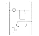
図1に、本発明の発光装置が有する画素の一実施形態を示す。図1に示す画素は、発光素
子104と、ビデオ信号の画素への入力を制御するためのスイッチング素子として用いる
トランジスタ(スイッチング用トランジスタ)101と、発光素子104に流れる電流値
を制御する駆動用トランジスタ102、発光素子104への電流の供給を制御する電流制
御用トランジスタ103とを有している。さらに本実施の形態のように、ビデオ信号の電
位を保持するための容量素子105を画素に設けても良い。
発明では、駆動用トランジスタ102を飽和領域で、電流制御用トランジスタ103を線
形領域で動作させる。
LをWと同じか、それより短くてもよい。より望ましくは、駆動用トランジスタ102の
Wに対するLの比が5以上にするとよい。また、駆動用トランジスタ102のチャネル長
をL1、チャネル幅をW1、電流制御用トランジスタ103のチャネル長をL2、チャネ
ル幅をW2とすると、L1/W1:L2/W2=X:1のとき、Xは5以上6000以下
とするのが望ましい。例としては、L1/W1=500μm/3μm、L2/W2=3μ
m/100μmという場合が挙げられる。
し、ディプリーション型トランジスタを用いてもよい。
トランジスタを用いてもよい。
ている。スイッチング用トランジスタ101のソースとドレインは、一方が信号線Si(
i=1〜x)に、もう一方が電流制御用トランジスタ103のゲートに接続されている。
駆動用トランジスタ102のゲートは第2の電源線Wi(i=1〜x)に接続されている
。そして駆動用トランジスタ102及び電流制御用トランジスタ103は、第1の電源線
Vi(i=1〜x)から供給される電流が、駆動用トランジスタ102及び電流制御用ト
ランジスタ103のドレイン電流として発光素子104に供給されるように、第1の電源
線Vi(i=1〜x)、発光素子104と接続されている。本実施の形態では、電流制御
用トランジスタ103のソースが第1の電源線Vi(i=1〜x)に接続され、駆動用ト
ランジスタ102のドレインが発光素子104の画素電極に接続される。
電流制御用トランジスタ103のドレインを発光素子104の画素電極に接続してもよい
。
、陽極が駆動用トランジスタ102と接続している場合、陽極が画素電極、陰極が対向電
極となる。発光素子104の対向電極と、第1の電源線Vi(i=1〜x)のそれぞれに
は、発光素子104に順バイアス方向の電流が供給されるように、電位差が設けられてい
る。なお、対向電極は第3の電源線に接続されている。
されており、もう一方は電流制御用トランジスタ103のゲートに接続されている。容量
素子105はスイッチング用トランジスタ101が非選択状態(オフ状態)にある時、容
量素子105の電極間の電位差を保持するために設けられている。なお図1では容量素子
105を設ける構成を示したが、本発明はこの構成に限定されず、容量素子105を設け
ない構成にしても良い。
ジスタとし、駆動用トランジスタ102のドレインと発光素子104の陽極とを接続した
。逆に駆動用トランジスタ102および電流制御用トランジスタ103をN型トランジス
タとするならば、駆動用トランジスタ102のソースと発光素子104の陰極とを接続す
る。この場合、発光素子104の陰極が画素電極、陽極が対向電極となる。
書き込み期間、データ保持期間とに分けて説明することができる。
=1〜y)にゲートが接続されているスイッチング用トランジスタ101がオンになる。
そして、信号線Si(i=1〜x)に入力されたビデオ信号が、スイッチング用トランジ
スタ101を介して電流制御用トランジスタ103のゲートに入力される。なお、駆動用
トランジスタ102はゲートが第1の電源線Vi(i=1〜x)に接続されているため、
常にオン状態である。
Vi(i=1〜x)を介して電流が発光素子104に供給される。このとき電流制御用ト
ランジスタ103は線形領域で動作しているため、発光素子104に流れる電流は、飽和
領域で動作する駆動用トランジスタ102と発光素子104の電圧電流特性によって決ま
る。そして発光素子104は、供給される電流に見合った高さの輝度で発光する。
104への電流の供給は行なわれず、発光素子104は発光しない。
トランジスタ101をオフにし、書き込み期間において書き込まれたビデオ信号の電位を
保持する。書き込み期間において電流制御用トランジスタ103をオンにした場合、ビデ
オ信号の電位は容量素子105によって保持されているので、発光素子104への電流の
供給は維持されている。逆に、書き込み期間において電流制御用トランジスタ103をオ
フにした場合、ビデオ信号の電位は容量素子105によって保持されているので、発光素
子104への電流の供給は行なわれていない。
の一形態に相当する。
れたトランジスタであっても良いし、SOIを用いたトランジスタであっても良いし、多
結晶シリコンやアモルファスシリコンを用いた薄膜トランジスタであっても良い。また、
有機半導体を用いたトランジスタであっても良いし、カーボンナノチューブを用いたトラ
ンジスタであってもよい。また本発明の発光装置の画素に設けられたトランジスタは、シ
ングルゲート構造を有していても良いし、ダブルゲート構造やそれ以上のゲート電極を有
するマルチゲート構造であっても良い。
トランジスタ103のソース・ドレイン間電圧Vdsは小さく、電流制御用トランジスタ
103のゲート・ソース間電圧Vgsの僅かな変動は、発光素子104に流れる電流に影
響しない。発光素子104に流れる電流は飽和領域で動作する駆動用トランジスタ102
により決定される。よって、電流制御用トランジスタ103のゲート・ソース間に設けら
れた容量素子105の容量を大きくしたり、スイッチング用トランジスタ101のオフ電
流を低く抑えなくても、発光素子104に流れる電流に影響しない。また、電流制御用ト
ランジスタ103のゲートにつく寄生容量による影響も受けない。このため、ばらつき要
因が減り、画質を大いに高めることができる。
供給をある程度維持することができるので、パネルの大型化、高精細化に柔軟に対応する
ことができ、今後の主流となりつつある。具体的に提案されている、アクティブマトリク
ス型発光装置における画素の構成は、発光装置のメーカーによって異なっており、それぞ
れに特色のある技術的工夫が凝らされている。図22に、アクティブマトリクス型の発光
装置における駆動方法の分類を、体系的に示す。
に、ビデオ信号がデジタルのものと、アナログのものとに分類できる。そしてアナログに
分類される発光装置は、さらに、発光素子に流す電流値をアナログ的に変調させる電流変
調と、インバータのオンとオフの長さを変化させることで、階調を表現する時間変調とに
分類される。電流変調の発光装置は、Tr特性補正回路ありのものと、なしのものに分類
できる。Tr特性補正回路とは、駆動用トランジスタの特性ばらつきを補正する回路であ
り、閾値のみ補正する回路や電流値(閾値、移動度等すべて含む)を補正する回路がある
。
で閾値補正をするものと、電流プログラミングで電流値補正をするものとに分類される。
電圧プログラミングは、ビデオ信号を電圧で入力し、駆動用トランジスタの閾値のばらつ
きを補正するものである。一方、電流プログラミングは、駆動用トランジスタの電流値(
閾値、移動度もすべて含む)のばらつきを補正するものである。ビデオ信号は電流で入力
する。発光素子は電流駆動素子であり、電流によって発光輝度が決まるのでデータとして
電流値を用いた方が直接的である。
電流ミラーを用いないタイプに分類される。電流ミラー型は、カレントミラー回路を利用
したピクセル回路で、電流を設定するトランジスタと発光素子への電流供給を行うトラン
ジスタを別々に配置する。ミラーとなる2つのトランジスタの特性が揃っていることが大
前提となる。電流ミラーを用いないタイプの発光装置は、カレントミラー回路を用いず、
1つのトランジスタで電流設定と発光素子への電流供給を行う。
は画素内にサブピクセルを設け、その発光面積に1:2:4:8:…のように重みをつけ
て、その選択により階調表示を行うものである。時間諧調は、1フレームを幾つかのサブ
フレームに分け、それぞれの発光時間に1:2:4:8:…のように重みをつけ、その選
択によって階調表示を行うものである。
、SES (Simultaneous Erasing Scan)駆動とに分類され
る。DPS駆動は、サブフレームがそれぞれ、データ書き込み期間(Addressin
g Period)と発光期間(Lighting Period)の2つの部分より構
成される。DPS駆動については、”M. Mizukami et al., 6−B
it Digital VGA OLED, SID ’00 Digest, p.
912”に記載されている。SES駆動は、消去用トランジスタを用いることで、データ
書き込み期間と発光期間を重ねることができ、発光素子の発光期間を長くすることができ
る。SES駆動については、”K. Inukai et al., 4.0−in.
TFT−OLED Displays and a Novel Digital Dr
iving Method, SID ’00 Digest, p. 924”に記載
されている。
を一定電流で駆動するものであり、発光素子の抵抗変化によらず、一定電流が流れる。定
電圧駆動は、発光素子を一定電圧で駆動するものである。
される。Tr特性補正回路ありの発光装置は、国際公開番号WO03/027997に記
載されている発光装置の駆動(CCT1)のものと、特願2002−056555号公報
に記載されている発光装置の駆動(CCSP)のものとがある。Tr特性補正回路なしの
発光装置は、さらに、駆動Tr ロングチャネル長のものと、発光時ゲート電位固定法の
ものとに分類される。駆動Tr ロングチャネル長については、特願2002−0250
65号公報に記載されている。駆動Tr ロングチャネル長は、定電流駆動時の駆動用ト
ランジスタの特性ばらつきを抑制するものである。ゲート長を超ロングにすることで、閾
値近傍のVgsを使わないため各画素の発光素子に流れる電流値のばらつきを低減できる
。
用トランジスタがオンする電位で固定することで、駆動用トランジスタのVgsを一定に
し、表示不良を改善するものである。データは駆動用トランジスタと直列に配置された電
流制御用トランジスタのゲートに入力される。そして発光時ゲート電位固定法の発光装置
の発光装置にも、駆動Tr ロングチャネル長のものがある。本発明の発光装置は、発光
時ゲート電位固定法の駆動Tr ロングチャネル長に分類される。
のか、電流を用いているのかで分類した、駆動方法の一覧を示す。図23に示すように、
発光素子の発光時において、画素に入力されるビデオ信号が定電圧(CV)のものと、定
電流(CC)のものとがある。
VCV)と、発光素子に流れる電流が一定のもの(CVCC)とがある。またビデオ信号
が定電流(CC)のものには、発光素子に印加される電圧が一定のもの(CCCV)と、
発光素子に流れる電流が一定のもの(CCCC)とがある。
本実施の形態では、本発明の発光装置が有する画素の、図1とは異なる形態について説
明する。
トランジスタ202と、電流制御用トランジスタ203と、電流制御用トランジスタ20
3を強制的にオフするためのトランジスタ(消去用トランジスタ)206とを有している
。上記素子に加えて容量素子205を画素に設けても良い。
発明では、駆動用トランジスタ202を飽和領域で、電流制御用トランジスタ203を線
形領域で動作させる。
LをWと同じか、それより短くてもよい。より望ましくは、駆動用トランジスタ202の
Wに対するLの比が5以上にするとよい。
し、ディプリーション型トランジスタを用いてもよい。
ジスタを用いてもよいし、P型トランジスタを用いてもよい。
接続されている。スイッチング用トランジスタ201のソースとドレインは、一方が信号
線Si(i=1〜x)に、もう一方が電流制御用トランジスタ203のゲートに接続され
ている。また消去用トランジスタ206のゲートは、第2の走査線Gej(j=1〜y)
に接続されており、ソースとドレインは、一方が第1の電源線Vi(i=1〜x)に、他
方が電流制御用トランジスタ203のゲートに接続されている。駆動用トランジスタ20
2のゲートは第2の電源線Wi(i=1〜x)に接続されている。そして駆動用トランジ
スタ202及び電流制御用トランジスタ203は、第1の電源線Vi(i=1〜x)から
供給される電流が、駆動用トランジスタ202及び電流制御用トランジスタ203のドレ
イン電流として発光素子204に供給されるように、第1の電源線Vi(i=1〜x)、
発光素子204と接続されている。本実施の形態では、電流制御用トランジスタ203の
ソースが第1の電源線Vi(i=1〜x)に接続され、駆動用トランジスタ202のドレ
インが発光素子204の画素電極に接続される。
電流制御用トランジスタ203のドレインを発光素子204の画素電極に接続してもよい
。
陽極が駆動用トランジスタ202と接続している場合、陽極が画素電極、陰極が対向電極
となる。発光素子204の対向電極と、第1の電源線Vi(i=1〜x)のそれぞれには
、発光素子204に順バイアス方向の電流が供給されるように、電位差が設けられている
。なお、対向電極は第3の電源線に接続されている。
されており、もう一方は電流制御用トランジスタ203のゲートに接続されている。
ジスタとし、駆動用トランジスタ202のドレインと発光素子204の陽極とを接続した
。逆に駆動用トランジスタ202および電流制御用トランジスタ203をN型トランジス
タとするならば、駆動用トランジスタ202のソースと発光素子204の陰極とを接続す
る。この場合、発光素子204の陰極が画素電極、陽極が対向電極となる。
明することができる。書き込み期間とデータ保持期間におけるスイッチング用トランジス
タ201、駆動用トランジスタ202及び電流制御用トランジスタ203の動作について
は、図1の場合と同様である。
03がオンの場合の動作を、図21(B)に、書き込み期間において電流制御用トランジ
スタ203がオフの場合の動作を示す。また図21(C)に、保持期間において電流制御
用トランジスタ203がオンの場合の動作を、図21(D)に、消去期間における動作を
示す。なお、図21(A)〜図21(D)では動作を分かり易くするために、スイッチン
グ素子として用いるスイッチング用トランジスタ201と、電流制御用トランジスタ20
3と、消去用トランジスタ206とをスイッチとして示す。
走査線Gaj(j=1〜y)にゲートが接続されているスイッチング用トランジスタ20
1がオンになる。そして、信号線Si(i=1〜x)に入力されたビデオ信号が、スイッ
チング用トランジスタ201を介して電流制御用トランジスタ203のゲートに入力され
る。なお、駆動用トランジスタ202はゲートが第1の電源線Vi(i=1〜x)に接続
されているため、常にオン状態である。
に示すように、第1の電源線Vi(i=1〜x)を介して電流が発光素子204に供給さ
れる。このとき電流制御用トランジスタ203は線形領域で動作しているため、発光素子
204に流れる電流は、飽和領域で動作する駆動用トランジスタ202と発光素子204
の電圧電流特性によって決まる。そして発光素子204は、供給される電流に見合った高
さの輝度で発光する。
がオフになる場合は、発光素子204への電流の供給は行なわれず、発光素子204は発
光しない。
ッチング用トランジスタ201をオフにし、書き込み期間において書き込まれたビデオ信
号の電位を保持する。書き込み期間において電流制御用トランジスタ203をオンにした
場合、ビデオ信号の電位は容量素子205によって保持されているので、図21(C)に
示すように、発光素子204への電流の供給は維持されている。逆に、書き込み期間にお
いて電流制御用トランジスタ203をオフにした場合、ビデオ信号の電位は容量素子20
5によって保持されているので、発光素子204への電流の供給は行なわれていない。
されて消去用トランジスタ206がオンになり、電源線Vi(i=1〜x)の電位が消去
用トランジスタ206を介して電流制御用トランジスタ203のゲートに与えられる。よ
って、電流制御用トランジスタ203がオフになるため、発光素子204に強制的に電流
が供給されない状態を作り出すことができる。
動について説明する。
010を有する。外部回路3004はA/D変換部3001、電源部3002及び信号生
成部3003を有する。A/D変換部3001はアナログ信号で入力された映像データ信
号をデジタル信号(ビデオ信号)に変換し、信号線駆動回路3006へ供給する。電源部
3002はバッテリーやコンセントより供給された電源から、それぞれ所望の電圧値の電
源を生成し、信号線駆動回路3006、走査線駆動回路3007、発光素子3011、信
号生成部3003等に供給する。信号生成部3003には、電源、映像信号及び同期信号
等が入力され、各種信号の変換を行う他、信号線駆動回路3006及び走査線駆動回路3
007を駆動するためのクロック信号等を生成する。
部3005から内部回路等に入力される。
れ、また、発光素子3011を有する。内部回路は信号線駆動回路3006、走査線駆動
回路3007及び画素部3009を有する。図3には例として実施形態1に記載の画素を
採用しているが、前記画素部3009に本発明の実施形態に挙げたいずれかの画素構成を
採用することができる。
走査線駆動回路3007が配置されている。発光素子3011及び、前記発光素子の対向
電極は画素部3009全体面に形成されている。
ジスタ4002、データラッチ回路4003、ラッチ回路4004、レベルシフタ400
5及びバッファ4006等を有する。
スタートパルス(S−SP)、ビデオ信号(DATA)及びラッチパルス(LatchP
ulse)とする。
フトレジスタ4002より、順次サンプリングパルスが出力される。サンプリングパルス
はデータラッチ回路4003へ入力され、そのタイミングで、ビデオ信号を取り込み、保
持する。この動作が一列目から順に行われる。
期間中にラッチパルスが入力され、データラッチ回路4003において保持されているビ
デオ信号は一斉にラッチ回路4004へと転送される。その後、レベルシフタ4005に
おいてレベルシフトされ、バッファ4006において整形された後、信号線S1からSn
へ一斉に出力される。その際、走査線駆動回路3007によって選択された行の画素へ、
Hレベル、Lレベルが入力され、発光素子3011の発光、非発光を制御する。
04が独立されているが、これらを同一基板上に一体形成して作製してもよい。また、表
示装置は例として、OLEDを使用したものとしたが、OLED以外の発光素子を利用し
た発光装置でもよい。また、信号線駆動回路3006内にレベルシフタ4005及びバッ
ファ4006が無くてもよい。
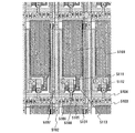
施例の画素の上面図を示す。
04は第1の走査線、5003は第2の走査線に相当する。本実施例では、信号線500
1と第1の電源線5002と第2の電源線5011は同じ導電膜で形成し、第1の走査線
5004と第2の走査線5003は同じ導電膜で形成する。また5005はスイッチング
用トランジスタであり、第1の走査線5004の一部がそのゲート電極として機能する。
また5006は消去用トランジスタであり、第2の走査線5003の一部がそのゲート電
極として機能する。5007は駆動用トランジスタ、5008は電流制御用トランジスタ
に相当する。駆動用トランジスタ5007は、そのL/Wが電流制御用トランジスタ50
08よりも大きくなるように、活性層が曲がりくねっている。例えば、駆動用トランジス
タ5007はL=200[nm]、W=4[nm]、電流制御用トランジスタ5008は
L=6[nm]、W=12[nm]のようなサイズにする。5009は画素電極に相当し
、電界発光層や陰極(共に図示せず)と重なる領域(発光エリア)5010において発光
する。
ない。
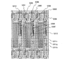
る。図8に本実施例の画素の上面図を示す。
04は第1の走査線、8003は第2の走査線に相当する。本実施例では、信号線800
1と第1の電源線8002と第2の電源線8011は同じ導電膜で形成し、第1の走査線
8004と第2の走査線8003は同じ導電膜で形成する。また8005はスイッチング
用トランジスタであり、第1の走査線8004の一部がそのゲート電極として機能する。
また8006は消去用トランジスタであり、第2の走査線8003の一部がそのゲート電
極として機能する。8007は駆動用トランジスタ、8008は電流制御用トランジスタ
に相当する。駆動用トランジスタ8007は、そのL/Wが電流制御用トランジスタ80
08よりも大きくなるように、活性層が曲がりくねっている。例えば、駆動用トランジス
タ8007はL=200[nm]、W=4[nm]、電流制御用トランジスタ8008は
L=6[nm]、W=12[nm]のようなサイズにする。8009は画素電極に相当し
、電界発光層や陰極(共に図示せず)と重なる領域(発光エリア)8010において発光
する。また、8012は容量手段であり、第2の電源線8011と電流制御用トランジス
タ8008との間のゲート絶縁膜によってなる。
ない。
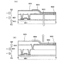
る光が陽極9023側に抜ける場合の、画素の断面図を示す。図9(A)では、発光素子
9022の陽極9023と駆動用トランジスタ9021が電気的に接続されており、陽極
9023上に電界発光層9024、陰極9025が順に積層されている。陰極9025は
仕事関数が小さく、なおかつ光を反射する導電膜であれば公知の材料を用いることができ
る。例えば、Ca、Al、CaF、MgAg、AlLi等が望ましい。そして電界発光層
9024は、単数の層で構成されていても、複数の層が積層されるように構成されていて
もどちらでも良い。複数の層で構成されている場合、陽極9023上にホール注入層、ホ
ール輸送層、発光層、電子輸送層、電子注入層の順に積層する。なおこれらの層を全て設
ける必要はない。陽極9023は光を透過する透明導電膜を用いて形成し、例えばITO
の他、酸化インジウムに2〜20%の酸化亜鉛(ZnO)を混合した透明導電膜を用いて
も良い。
子9022に相当する。図9(A)に示した画素の場合、発光素子9022から発せられ
る光は、白抜きの矢印で示すように陽極9023側に抜ける。
る光が陽極9005側に抜ける場合の、画素の断面図を示す。図9(B)では、発光素子
9002の陰極9003と駆動用トランジスタ9001が電気的に接続されており、陰極
9003上に電界発光層9004、陽極9005が順に積層されている。陰極9003は
仕事関数が小さく、なおかつ光を反射する導電膜であれば公知の材料を用いることができ
る。例えば、Ca、Al、CaF、MgAg、AlLi等が望ましい。そして電界発光層
9004は、単数の層で構成されていても、複数の層が積層されるように構成されていて
もどちらでも良い。複数の層で構成されている場合、陰極9003上に電子注入層、電子
輸送層、発光層、ホール輸送層、ホール注入層の順に積層する。なおこれらの層を全て設
ける必要はない。陽極9005は光を透過する透明導電膜を用いて形成し、例えばITO
の他、酸化インジウムに2〜20%の酸化亜鉛(ZnO)を混合した透明導電膜を用いて
も良い。
子9002に相当する。図9(B)に示した画素の場合、発光素子9002から発せられ
る光は、白抜きの矢印で示すように陽極9005側に抜ける。
たが、駆動用トランジスタと発光素子との間に電流制御用トランジスタが接続されている
構成であってもよい。
。データ保持期間Ts1〜Ts4は、その長さの比をTs1:Ts2:Ts3:Ts4=
23:22:21:20=8:4:2:1としている。
査線が選択され、スイッチング用トランジスタがオンする。次に、信号線よりビデオ信号
が各画素に入力され、その電位によって各画素の発光、非発光が制御される。ビデオ信号
の書き込みが完了した行においては、直ちにデータ保持期間Ts1へと移る。同じ動作が
、最終行まで行われ、期間Ta1が終了する。このとき、データ保持期間Ts1が終了し
た行から順に書き込み期間Tb2へ移る。
Ts4が該当する)においては、データ保持期間の終了後、直ちに次の期間が開始しない
よう、消去期間2102を設ける。消去期間において発光素子は、強制的に非発光状態と
される。
に限定されない。また、発光の順番はTs1〜Ts4である必要はなく、ランダムでもよ
いし、複数に分割して発光をしてもよい。
去パルス1に示すように、1行ずつパルスを入力し、消去期間中は容量手段等によって保
持してもよいし、消去パルス2に示すように、消去期間中ずっと、Hレベルを入力しつづ
けてもよい。尚、図10(B)に示すパルスはいずれもスイッチング用トランジスタ及び
消去用トランジスタがN型である場合であり、前記スイッチング用トランジスタ及び前記
消去用トランジスタがP型である場合は、図10(B)のパルスはいずれもHレベルとL
レベルが反転する。
特に低消費電力が要求されるモバイル機器には本発明の表示装置を用いることが望ましい
。
型ゲーム機または電子書籍等)、ビデオカメラ、デジタルカメラ、ゴーグル型ディスプレ
イ、表示ディスプレイ、ナビゲーションシステム等が挙げられる。これら電子機器の具体
例を図6に示す。
03等を含む。本発明の発光装置は表示部6003に用いることができる。表示装置は、
パソコン用、TV放送受信用、広告表示用など全ての情報表示装置が含まれる。
6103、操作ボタン6104、外部インターフェイス6105等を含む。本発明の発光
装置は表示部6103に用いることができる。
を含む。本発明の発光装置は表示部6202に用いることができる。
3、表示部6304、操作スイッチ6305、アンテナ6306等を含む。本発明の発光
装置は表示部6304に用いることができる。
用いることが可能である。
基板7000上に形成されている駆動用トランジスタ7001を示す。駆動用トランジス
タ7001は第1の層間絶縁膜7002で覆われており、第1の層間絶縁膜7002上に
は樹脂等で形成されたカラーフィルタ7003と、コンタクトホールを介して駆動用トラ
ンジスタ7001のドレインと電気的に接続されている配線7004が形成されている。
なお、駆動用トランジスタ7001と配線7004の間に電流制御用トランジスタが設け
られていても良い。
02上に、第2の層間絶縁膜7005が形成されている。なお、第1の層間絶縁膜700
2または第2の層間絶縁膜7005は、プラズマCVD法またはスパッタ法を用い、酸化
珪素、窒化珪素または酸化窒化珪素膜を単層でまたは積層して用いることができる。また
酸素よりも窒素のモル比率が高い酸化窒化珪素膜上に、窒素よりも酸素のモル比率が高い
酸化窒化珪素膜を積層した膜を第1の層間絶縁膜7002または第2の層間絶縁膜700
5として用いても良い。或いは第1の層間絶縁膜7002または第2の層間絶縁膜700
5として、有機樹脂膜を用いても良い。
接続されている配線7006が形成されている。配線7006の一部は発光素子の陽極と
して機能している。配線7006は、第2の層間絶縁膜7005を間に挟んで、カラーフ
ィルタ7003と重なる位置に形成する。
ている。有機樹脂膜7008は開口部を有しており、該開口部において陽極として機能す
る配線7006と電界発光層7009と陰極7010が重なり合うことで発光素子701
1が形成されている。電界発光層7009は、発光層単独かもしくは発光層を含む複数の
層が積層された構成を有している。なお、有機樹脂膜7008及び陰極7010上に、保
護膜を成膜しても良い。この場合、保護膜は水分や酸素などの発光素子の劣化を促進させ
る原因となる物質を、他の絶縁膜と比較して透過させにくい膜を用いる。代表的には、例
えばDLC膜、窒化炭素膜、RFスパッタ法で形成された窒化珪素膜等を用いるのが望ま
しい。また上述した水分や酸素などの物質を透過させにくい膜と、該膜に比べて水分や酸
素などの物質を透過させやすい膜とを積層させて、保護膜として用いることも可能である
。
素等を除去するために真空雰囲気下で加熱しておく。具体的には、100℃〜200℃、
0.5〜1時間程度、真空雰囲気下で加熱処理を行なう。望ましくは3×10⁻⁷Tor
r以下とし、可能であるならば3×10⁻⁸Torr以下とするのが最も望ましい。そし
て、有機樹脂膜に真空雰囲気下で加熱処理を施した後に電界発光層を成膜する場合、成膜
直前まで真空雰囲気下に保つことで、信頼性をより高めることができる。
て形成されている電界発光層7009に、該端部において穴があかないように、丸みを帯
びさせることが望ましい。具体的には、開口部における有機樹脂膜の断面が描いている曲
線の曲率半径が、0.2〜2μm程度であることが望ましい。
き、配線7006と陰極7010が電界発光層7009に形成された穴においてショート
するのを防ぐことができる。また電界発光層7009の応力を緩和させることで、発光領
域が減少するシュリンクとよばれる不良を低減させることができ、信頼性を高めることが
できる。
例を示している。感光性の有機樹脂には、光、電子、イオンなどのエネルギー線が露光さ
れた箇所が除去されるポジ型と、露光された箇所が残るネガ型とがある。本発明ではネガ
型の有機樹脂膜を用いても良い。また感光性のポリイミドを用いて有機樹脂膜7008を
形成しても良い。ネガ型のアクリルを用いて有機樹脂膜7008を形成した場合、開口部
における端部が、S字状の断面形状となる。このとき開口部の上端部及び下端部における
曲率半径は、0.2〜2μmとすることが望ましい。
20%の酸化亜鉛(ZnO)を混合した透明導電膜を用いても良い。図11では配線70
06としITOを用いている。配線7006は、その表面が平坦化されるように、CMP
法、ポリビニルアルコール系の多孔質体で拭浄して研磨しても良い。またCMP法を用い
た研磨後に、配線7006の表面に紫外線照射、酸素プラズマ処理などを行ってもよい。
公知の他の材料を用いる。例えば、Ca、Al、CaF、MgAg、AlLi等が望まし
い。なお陰極側から光を得るためには、膜厚を薄くする方法の他に、Liを添加すること
で仕事関数が小さくなったITOを用いる方法もある。本発明で用いる発光素子は、陽極
側と陰極側の両方から光が発せられる構成であれば良い。
脱ガスの少ない保護フィルム(ラミネートフィルム、紫外線硬化樹脂フィルム等)や透光
性のカバー材7012でパッケージング(封入)することが好ましい。その際、カバー材
の内部を不活性雰囲気にしたり、内部に吸湿性材料(例えば酸化バリウム)を配置したり
すると発光素子の信頼性が向上する。そして本発明では、カバー材7012にカラーフィ
ルタ7013を設けても良い。
能である。
ランジスタ203の位置を入れ替えた場合の、画素の構成について説明する
いては、図12においても同じ符号を付して示す。図12に示した画素と図2に示した画
素は、第1の電源線Vi(i=1〜x)から供給される電流が、駆動用トランジスタ20
2及び電流制御用トランジスタ203のドレイン電流として、発光素子204に供給され
るところは同じである。ただし図12では、駆動用トランジスタ202のソースが第1の
電源線Vi(i=1〜x)に接続され、電流制御用トランジスタのドレインが発光素子2
04の画素電極に接続されている点において、図2に示す画素と異なっている。
ことで、駆動用トランジスタ202のゲート・ソース間電圧Vgsが固定される。つまり
、発光素子204が劣化しても、当然、飽和領域で動作する駆動用トランジスタ202の
ゲート・ソース間電圧Vgsは変動せずに固定されたままである。よって、本実施例では
、発光素子204が劣化しても、飽和領域で動作する駆動用トランジスタ202のドレイ
ン電流が変動するのを防ぐことができる。
実施例では、図12に示した画素において、発光素子204の画素電極と電流制御用トラ
ンジスタ203のドレインとの間に抵抗を設ける例について示す。図13に本実施例の画
素の上面図を示す。
04は第1の走査線、5103は第2の走査線に相当する。本実施例では、信号線510
1と第1の電源線5102と第2の電源線5111は同じ導電膜で形成し、第1の走査線
5104と第2の走査線5103は同じ導電膜で形成する。また5105はスイッチング
用トランジスタであり、第1の走査線5104の一部がそのゲート電極として機能する。
また5106は消去用トランジスタであり、第2の走査線5103の一部がそのゲート電
極として機能する。5107は駆動用トランジスタ、5108は電流制御用トランジスタ
に相当する。また5112は容量素子に相当し、5113は半導体膜で形成された抵抗に
相当する。駆動用トランジスタ5107は、そのL/Wが電流制御用トランジスタ510
8よりも大きくなるように、活性層が曲がりくねっている。例えば、駆動用トランジスタ
5107はL=200[nm]、W=4[nm]、電流制御用トランジスタ5108はL
=6[nm]、W=12[nm]のようなサイズにする。5109は画素電極に相当し、
画素電極5109と、電界発光層(図示せず)と、陰極(図示せず)とが重なる領域(発
光エリア)において、発光する。
した後、該導電膜をパターニングして画素電極を形成する前において、該導電膜に帯電し
た電荷により駆動用トランジスタ5107のドレインの電位が急激に変化し、駆動用トラ
ンジスタ5107が破壊されるのを防ぐことができる。また、ELが蒸着されるまでの静
電対策として用いることができる。
ない。
2走査線Gej(j=1〜y)を共有している画素が、さらに第2の電源線Wi(i=1
〜x)を共有している場合の、画素の構成について説明する。
線については、図14(A)においても同じ符号を付して示す。ただし図14(A)では
、第1の走査線Gaj(j=1〜y)と、第2の走査線Gej(j=1〜y)とを共有し
ている画素が、さらに、第2の電源線Wj(j=1〜x)を共有している。そして第2の
電源線Wj(j=1〜x)が、信号線Si(i=1〜x)及び第1の電源線Vi(i=1
〜x)と交差しており、同じ第2の走査線Gej(j=1〜y)を共有している画素は、
互いに異なる信号線Si(i=1〜x)を有している。
のゲートに印加される電圧を、赤色、緑色、青色の画素ごとに分けることで、ホワイトバ
ランス調節する方法を採用した場合の、画素の構成を示す。図14(B)では、赤色に対
応した画素210において、赤色(R)用の第2の電源線Wrjが、駆動用トランジスタ
202のゲートに接続されている。また、緑色に対応した画素211において、緑色(G
)用の第2の電源線Wgjが、駆動用トランジスタ202のゲートに接続されている。ま
た、青色に対応した画素212において、青色(B)用の第2の電源線Wbjが、駆動用
トランジスタ202のゲートに接続されている。
トランジスタ202のドレインとの間に抵抗を設けた場合の、画素の構成について説明す
る。
A)において既に示した素子や配線については、図15(A)においても同じ符号を付し
て示す。図15(A)は図14(A)と異なり、発光素子204の画素電極と駆動用トラ
ンジスタ202のドレインとの間に、抵抗209を有する。
のゲートに印加される電圧を、赤色、緑色、青色の画素ごとに分けることで、ホワイトバ
ランス調節する方法を採用した場合の、画素の構成を示す。図15(B)では、赤色に対
応した画素210において、赤色(R)用の第2の電源線Wrjが、駆動用トランジスタ
202のゲートに接続されている。また、緑色に対応した画素211において、緑色(G
)用の第2の電源線Wgjが、駆動用トランジスタ202のゲートに接続されている。ま
た、青色に対応した画素212において、青色(B)用の第2の電源線Wbjが、駆動用
トランジスタ202のゲートに接続されている。
後、該導電膜をパターニングして画素電極を形成する前において、該導電膜に帯電した電
荷により駆動用トランジスタ202のドレインの電位が急激に変化し、駆動用トランジス
タ202が破壊されるのを防ぐことができる。また、ELが蒸着されるまでの静電対策と
して用いることができる。
実施例の画素の上面図を示す。
04は第1の走査線、5203は第2の走査線に相当する。本実施例では、信号線520
1と第1の電源線5202は同じ導電膜で形成し、第1の走査線5204と第2の走査線
5203と第2の電源線5211は同じ導電膜で形成する。また5205はスイッチング
用トランジスタであり、第1の走査線5204の一部がそのゲート電極として機能する。
また5206は消去用トランジスタであり、第2の走査線5203の一部がそのゲート電
極として機能する。5207は駆動用トランジスタ、5208は電流制御用トランジスタ
に相当する。また、5212は容量素子に相当し、5213は半導体膜で形成された抵抗
に相当する。駆動用トランジスタ5207は、そのL/Wが電流制御用トランジスタ52
08よりも大きくなるように、活性層が曲がりくねっている。例えば、駆動用トランジス
タ5207はL=200[nm]、W=4[nm]、電流制御用トランジスタ5208は
L=6[nm]、W=12[nm]のようなサイズにする。5209は画素電極に相当し
、画素電極5209と、電界発光層(図示せず)と、陰極(図示せず)とが重なる領域(
発光エリア)において、発光する。
実施例の画素の上面図を示す。
の電源線、5311gは緑色の画素に対応する第2の電源線、5311bは青色の画素に
対応する第2の電源線に相当し、5304は第1の走査線、5303は第2の走査線に相
当する。本実施例では、信号線5301と第1の電源線5302は同じ導電膜で形成し、
第1の走査線5304と第2の走査線5303と第2の電源線5311r、5311g、
5311bは同じ導電膜で形成する。また5305はスイッチング用トランジスタであり
、第1の走査線5304の一部がそのゲート電極として機能する。また5306は消去用
トランジスタであり、第2の走査線5303の一部がそのゲート電極として機能する。5
307は駆動用トランジスタ、5308は電流制御用トランジスタに相当する。また、5
312は容量素子に相当し、5313は半導体膜で形成された抵抗に相当する。駆動用ト
ランジスタ5307は、そのL/Wが電流制御用トランジスタ5308よりも大きくなる
ように、活性層が曲がりくねっている。例えば、駆動用トランジスタ5307はL=20
0[nm]、W=4[nm]、電流制御用トランジスタ5308はL=6[nm]、W=
12[nm]のようなサイズにする。5309は画素電極に相当し、画素電極5309と
、電界発光層(図示せず)と、陰極(図示せず)とが重なる領域(発光エリア)において
、発光する。
ない。
4.3インチ、隣接する発光素子を分離するための、隔壁として用いる層間膜の幅を20
μmとし、VGA(640×480)200dpiで、画素のサイズを45×135μm
とすることができる。
れる光が陰極9013側に抜ける場合の、画素の断面図を示す。図18(A)では、駆動
用トランジスタ9011のドレインと電気的に接続された透明導電膜9017上に、発光
素子9012の陰極9013が成膜されており、陰極9013上に電界発光層9014、
陽極9015が順に積層されている。そして陽極9015を覆うように、光を反射または
遮蔽するための遮蔽膜9016が成膜されている。陰極9013は、仕事関数が小さく、
なおかつ光を反射する導電膜であれば公知の材料を用いることができる。例えば、Ca、
Al、CaF、MgAg、AlLi等が望ましい。ただしその膜厚は、光を透過する程度
とする。例えば20nmの膜厚を有するAlを、陰極9013として用いることができる
。そして電界発光層9014は、単数の層で構成されていても、複数の層が積層されるよ
うに構成されていてもどちらでも良い。陽極9015は光を透過する必要はないが、例え
ばITO、ITSO、酸化インジウムに2〜20%の酸化亜鉛(ZnO)を混合したIZ
O等の透明導電膜を用いても良いし、TiまたはTiNを用いても良い。そして遮蔽膜9
016は、例えば光を反射する金属等を用いることができるが、金属膜に限定されない。
例えば黒の顔料を添加した樹脂等を用いることもできる。
子9012に相当する。図18(A)に示した画素の場合、発光素子9012から発せら
れる光は、白抜きの矢印で示すように陰極9013側に抜ける。
れる光が陰極9035側に抜ける場合の、画素の断面図を示す。図18(B)では、駆動
用トランジスタ9031のドレインと電気的に接続された配線9036上に、発光素子9
032の陽極9033が成膜されており、陽極9033上に電界発光層9034、陰極9
035が順に積層されている。上記構成によって、陽極9033において光が透過しても
、該光は配線9036において反射される。陰極9035は、図18(A)の場合と同様
に、仕事関数が小さい導電膜であれば公知の材料を用いることができる。ただしその膜厚
は、光を透過する程度とする。例えば20nmの膜厚を有するAlを、陰極9035とし
て用いることができる。そして電界発光層9034は、図18(A)と同様に、単数の層
で構成されていても、複数の層が積層されるように構成されていてもどちらでも良い。陽
極9033は光を透過する必要はないが、図18(A)と同様に、透明導電膜を用いて形
成することができるし、TiNまたはTiを用いることもできる。
子9032に相当する。図18(B)に示した画素の場合、発光素子9032から発せら
れる光は、白抜きの矢印で示すように陰極9035側に抜ける。
たが、駆動用トランジスタと発光素子との間に電流制御用トランジスタが接続されている
構成であってもよい。
場合の、画素の断面構造について説明する。
いても良い。アモルファスシリコンでトランジスタを形成すると、結晶化のプロセスを設
けずに済むので、作製方法を簡略化することができ、低コスト化が図れる。ただしアモル
ファスシリコンで形成されたトランジスタはP型よりもN型の方が移動度は高く、発光装
置の画素に用いるのにより適している。本実施例では、駆動用トランジスタがN型の場合
における、画素の断面構造について説明する。
502は電流制御用トランジスタに相当する。駆動用トランジスタ6501は、絶縁表面
を有する基板6500上に形成されたゲート電極6503と、ゲート電極6503を覆う
ように基板6500上に形成されたゲート絶縁膜6504と、ゲート絶縁膜6504を間
に挟んでゲート電極6503と重なる位置に形成された半導体膜6505とを有している
。半導体膜6505は、ソース又はドレインとして機能する、導電型を付与する不純物が
添加された2つの不純物領域6506a、6506bを有している。そして不純物領域6
506aは配線6508と接続されている。
を有する基板6500上に形成されたゲート電極6510と、ゲート電極6510を覆う
ように基板6500上に形成されたゲート絶縁膜6504と、ゲート絶縁膜6504を間
に挟んでゲート電極6510と重なる位置に形成された半導体膜6511とを有している
。半導体膜6511は、ソース又はドレインとして機能する、導電型を付与する不純物が
添加された2つの不純物領域6512a、6512bを有している。そして不純物領域6
512aは、配線6513を介して駆動用トランジスタ6501が有する不純物領域65
06bと接続されている。
成された保護膜6507で覆われている。そして、保護膜6507に形成されたコンタク
トホールを介して、配線6508が陽極6509と接続されている。また、駆動用トラン
ジスタ6501及び電流制御用トランジスタ6502と、保護膜6507は層間絶縁膜6
520で覆われている。層間絶縁膜6520は開口部を有しており、該開口部において陽
極6509が露出している。陽極6509上には電界発光層6521と、陰極6522が
形成されている。
ある場合について説明したが、P型であってもよい。この場合、駆動用トランジスタの閾
値を制御するための不純物はP型を用いる。
実施例の画素の上面図を示す。
に相当し、5404は第1の走査線、5403は第2の走査線に相当する。本実施例では
、信号線5401と第1の電源線5402と第2の電源線5411aは同じ導電膜で形成
し、第1の走査線5404と第2の走査線5403と第2の電源線5411bは同じ導電
膜で形成する。また5405はスイッチング用トランジスタであり、第1の走査線540
4の一部がそのゲート電極として機能する。また5406は消去用トランジスタであり、
第2の走査線5403の一部がそのゲート電極として機能する。5407は駆動用トラン
ジスタ、5408は電流制御用トランジスタに相当する。また5412は容量素子に相当
し、5413は半導体膜で形成された抵抗に相当する。駆動用トランジスタ5407は、
そのL/Wが電流制御用トランジスタ5408よりも大きくなるように、活性層が曲がり
くねっている。例えば、駆動用トランジスタ5407はL=200[nm]、W=4[n
m]、電流制御用トランジスタ5408はL=6[nm]、W=12[nm]のようなサ
イズにする。5409は画素電極に相当し、画素電極5409と、電界発光層(図示せず
)と、陰極(図示せず)と重なる領域(発光エリア)5410において、発光する。
ない。
Claims (1)
- 第1のトランジスタと、
第2のトランジスタと、
発光素子と、
前記発光素子の発光又は非発光を制御する電位を供給する機能を有する第1の配線と、
前記発光素子に流れる電流を決定する電位を供給する機能を有する第2の配線と、
電源電位を供給する機能を有する第3の配線と、を有し、
前記第1のトランジスタのゲートは、前記第1の配線と電気的に接続され、
前記第1のトランジスタのソース又はドレインの一方は、前記発光素子と電気的に接続され、
前記第1のトランジスタのソース又はドレインの他方は、前記第2のトランジスタのソース又はドレインの一方と電気的に接続され、
前記第2のトランジスタのゲートは、前記第2の配線と電気的に接続され、
前記第2のトランジスタのソース又はドレインの他方は、前記第3の配線と電気的に接続され、
前記第1のトランジスタの半導体層は、チャネル長がチャネル幅と同じ、又は、前記チャネル長が前記チャネル幅より短く、
前記第2のトランジスタの半導体層は、チャネル長がチャネル幅より長く、且つ、チャネル形成領域が曲がりくねった形状を有し、
前記第3の配線は、前記第2のトランジスタの半導体層と重なるように配置されており、
前記第1のトランジスタは、発光時に線形領域で動作し、
前記第2のトランジスタは、前記発光時に飽和領域で動作することを特徴とする発光装置。
Priority Applications (1)
| Application Number | Priority Date | Filing Date | Title |
|---|---|---|---|
| JP2015151759A JP6101317B2 (ja) | 2003-03-26 | 2015-07-31 | 発光装置 |
Applications Claiming Priority (7)
| Application Number | Priority Date | Filing Date | Title |
|---|---|---|---|
| JP2003086500 | 2003-03-26 | ||
| JP2003086500 | 2003-03-26 | ||
| JP2003139560 | 2003-05-16 | ||
| JP2003139560 | 2003-05-16 | ||
| JP2003174134 | 2003-06-18 | ||
| JP2003174134 | 2003-06-18 | ||
| JP2015151759A JP6101317B2 (ja) | 2003-03-26 | 2015-07-31 | 発光装置 |
Related Parent Applications (1)
| Application Number | Title | Priority Date | Filing Date |
|---|---|---|---|
| JP2015084882A Division JP5966052B2 (ja) | 2003-03-26 | 2015-04-17 | 発光装置及びその作製方法 |
Related Child Applications (1)
| Application Number | Title | Priority Date | Filing Date |
|---|---|---|---|
| JP2016199603A Division JP2017058685A (ja) | 2003-03-26 | 2016-10-10 | 表示装置 |
Publications (2)
| Publication Number | Publication Date |
|---|---|
| JP2015212843A JP2015212843A (ja) | 2015-11-26 |
| JP6101317B2 true JP6101317B2 (ja) | 2017-03-22 |
Family
ID=33101960
Family Applications (13)
| Application Number | Title | Priority Date | Filing Date |
|---|---|---|---|
| JP2005504008A Expired - Fee Related JP4166783B2 (ja) | 2003-03-26 | 2004-03-17 | 発光装置及び素子基板 |
| JP2008077366A Withdrawn JP2008171021A (ja) | 2003-03-26 | 2008-03-25 | 表示装置 |
| JP2010274269A Expired - Fee Related JP5159868B2 (ja) | 2003-03-26 | 2010-12-09 | 表示装置 |
| JP2012249171A Expired - Fee Related JP5586678B2 (ja) | 2003-03-26 | 2012-11-13 | 表示装置 |
| JP2013244048A Expired - Lifetime JP5984785B2 (ja) | 2003-03-26 | 2013-11-26 | 発光装置 |
| JP2015084882A Expired - Fee Related JP5966052B2 (ja) | 2003-03-26 | 2015-04-17 | 発光装置及びその作製方法 |
| JP2015151759A Expired - Fee Related JP6101317B2 (ja) | 2003-03-26 | 2015-07-31 | 発光装置 |
| JP2016199603A Withdrawn JP2017058685A (ja) | 2003-03-26 | 2016-10-10 | 表示装置 |
| JP2018105903A Withdrawn JP2018146981A (ja) | 2003-03-26 | 2018-06-01 | 発光装置 |
| JP2019218210A Withdrawn JP2020038394A (ja) | 2003-03-26 | 2019-12-02 | 発光装置 |
| JP2021135631A Withdrawn JP2021185430A (ja) | 2003-03-26 | 2021-08-23 | 発光装置および素子基板 |
| JP2022035130A Expired - Lifetime JP7235907B2 (ja) | 2003-03-26 | 2022-03-08 | 発光装置 |
| JP2022143529A Withdrawn JP2022173273A (ja) | 2003-03-26 | 2022-09-09 | 発光装置 |
Family Applications Before (6)
| Application Number | Title | Priority Date | Filing Date |
|---|---|---|---|
| JP2005504008A Expired - Fee Related JP4166783B2 (ja) | 2003-03-26 | 2004-03-17 | 発光装置及び素子基板 |
| JP2008077366A Withdrawn JP2008171021A (ja) | 2003-03-26 | 2008-03-25 | 表示装置 |
| JP2010274269A Expired - Fee Related JP5159868B2 (ja) | 2003-03-26 | 2010-12-09 | 表示装置 |
| JP2012249171A Expired - Fee Related JP5586678B2 (ja) | 2003-03-26 | 2012-11-13 | 表示装置 |
| JP2013244048A Expired - Lifetime JP5984785B2 (ja) | 2003-03-26 | 2013-11-26 | 発光装置 |
| JP2015084882A Expired - Fee Related JP5966052B2 (ja) | 2003-03-26 | 2015-04-17 | 発光装置及びその作製方法 |
Family Applications After (6)
| Application Number | Title | Priority Date | Filing Date |
|---|---|---|---|
| JP2016199603A Withdrawn JP2017058685A (ja) | 2003-03-26 | 2016-10-10 | 表示装置 |
| JP2018105903A Withdrawn JP2018146981A (ja) | 2003-03-26 | 2018-06-01 | 発光装置 |
| JP2019218210A Withdrawn JP2020038394A (ja) | 2003-03-26 | 2019-12-02 | 発光装置 |
| JP2021135631A Withdrawn JP2021185430A (ja) | 2003-03-26 | 2021-08-23 | 発光装置および素子基板 |
| JP2022035130A Expired - Lifetime JP7235907B2 (ja) | 2003-03-26 | 2022-03-08 | 発光装置 |
| JP2022143529A Withdrawn JP2022173273A (ja) | 2003-03-26 | 2022-09-09 | 発光装置 |
Country Status (7)
| Country | Link |
|---|---|
| US (7) | US8026877B2 (ja) |
| EP (1) | EP1607931B1 (ja) |
| JP (13) | JP4166783B2 (ja) |
| KR (1) | KR101138806B1 (ja) |
| CN (1) | CN102709478B (ja) |
| TW (1) | TWI356389B (ja) |
| WO (1) | WO2004086343A1 (ja) |
Families Citing this family (80)
| Publication number | Priority date | Publication date | Assignee | Title |
|---|---|---|---|---|
| US6753654B2 (en) | 2001-02-21 | 2004-06-22 | Semiconductor Energy Laboratory Co., Ltd. | Light emitting device and electronic appliance |
| JP2004361424A (ja) * | 2003-03-19 | 2004-12-24 | Semiconductor Energy Lab Co Ltd | 素子基板、発光装置及び発光装置の駆動方法 |
| JP4842381B2 (ja) * | 2003-03-26 | 2011-12-21 | 株式会社半導体エネルギー研究所 | 半導体装置 |
| WO2004086343A1 (ja) | 2003-03-26 | 2004-10-07 | Semiconductor Energy Laboratory Co., Ltd. | 素子基板及び発光装置 |
| TWI363573B (en) * | 2003-04-07 | 2012-05-01 | Semiconductor Energy Lab | Electronic apparatus |
| US7250720B2 (en) * | 2003-04-25 | 2007-07-31 | Semiconductor Energy Laboratory Co., Ltd. | Display device |
| JP4754772B2 (ja) * | 2003-05-16 | 2011-08-24 | 株式会社半導体エネルギー研究所 | 発光装置及び該発光装置を用いた電子機器 |
| JP4755293B2 (ja) * | 2003-05-16 | 2011-08-24 | 株式会社半導体エネルギー研究所 | 発光装置及び電子機器 |
| JP4425574B2 (ja) | 2003-05-16 | 2010-03-03 | 株式会社半導体エネルギー研究所 | 素子基板及び発光装置 |
| JP4801329B2 (ja) * | 2003-06-18 | 2011-10-26 | 株式会社半導体エネルギー研究所 | 発光装置 |
| JP4641710B2 (ja) * | 2003-06-18 | 2011-03-02 | 株式会社半導体エネルギー研究所 | 表示装置 |
| US8552933B2 (en) * | 2003-06-30 | 2013-10-08 | Semiconductor Energy Laboratory Co., Ltd. | Light emitting device and driving method of the same |
| JP4583732B2 (ja) * | 2003-06-30 | 2010-11-17 | 株式会社半導体エネルギー研究所 | 表示装置、及びその駆動方法 |
| US8884845B2 (en) * | 2003-10-28 | 2014-11-11 | Semiconductor Energy Laboratory Co., Ltd. | Display device and telecommunication system |
| JP4841831B2 (ja) * | 2003-12-02 | 2011-12-21 | 株式会社半導体エネルギー研究所 | 表示装置及びその駆動方法 |
| US7683860B2 (en) * | 2003-12-02 | 2010-03-23 | Semiconductor Energy Laboratory Co., Ltd. | Display device, driving method thereof, and element substrate |
| US7595775B2 (en) * | 2003-12-19 | 2009-09-29 | Semiconductor Energy Laboratory Co., Ltd. | Light emitting display device with reverse biasing circuit |
| JP5099974B2 (ja) * | 2004-01-30 | 2012-12-19 | 株式会社半導体エネルギー研究所 | 発光装置 |
| US7446742B2 (en) | 2004-01-30 | 2008-11-04 | Semiconductor Energy Laboratory Co., Ltd. | Light emitting device |
| US8378930B2 (en) * | 2004-05-28 | 2013-02-19 | Sony Corporation | Pixel circuit and display device having symmetric pixel circuits and shared voltage lines |
| US20060066198A1 (en) * | 2004-09-24 | 2006-03-30 | Matsushita Toshiba Picture Display Co., Ltd. | Electron source apparatus |
| DE102004059506B3 (de) * | 2004-12-10 | 2006-08-17 | X-Fab Semiconductor Foundries Ag | Anordnung zum Test von eingebetteten Schaltungen mit Hilfe einer separaten Versorgungsspannung |
| JP2006208743A (ja) * | 2005-01-28 | 2006-08-10 | Sony Corp | 画素回路及び表示装置 |
| TWI505473B (zh) * | 2005-01-28 | 2015-10-21 | 半導體能源研究所股份有限公司 | 半導體裝置,電子裝置,和半導體裝置的製造方法 |
| JP4934964B2 (ja) * | 2005-02-03 | 2012-05-23 | ソニー株式会社 | 表示装置、画素駆動方法 |
| JP2006284915A (ja) * | 2005-03-31 | 2006-10-19 | Toshiba Matsushita Display Technology Co Ltd | 表示装置及びアレイ基板 |
| TW200701167A (en) * | 2005-04-15 | 2007-01-01 | Seiko Epson Corp | Electronic circuit, and driving method, electrooptical device, and electronic apparatus thereof |
| JP4770267B2 (ja) * | 2005-05-23 | 2011-09-14 | セイコーエプソン株式会社 | 表示方法および表示装置 |
| JP4797555B2 (ja) * | 2005-10-11 | 2011-10-19 | ソニー株式会社 | 表示装置及びその駆動方法 |
| JP4939045B2 (ja) * | 2005-11-30 | 2012-05-23 | セイコーエプソン株式会社 | 発光装置および電子機器 |
| CN102176304B (zh) * | 2005-12-02 | 2013-07-03 | 株式会社半导体能源研究所 | 半导体器件 |
| EP1793264A1 (en) * | 2005-12-05 | 2007-06-06 | Semiconductor Energy Laboratory Co., Ltd. | Liquid crystal display device |
| WO2007072766A1 (en) * | 2005-12-22 | 2007-06-28 | Semiconductor Energy Laboratory Co., Ltd. | Display device |
| EP1804114B1 (en) | 2005-12-28 | 2014-03-05 | Semiconductor Energy Laboratory Co., Ltd. | Display device |
| EP1832915B1 (en) * | 2006-01-31 | 2012-04-18 | Semiconductor Energy Laboratory Co., Ltd. | Display device with improved contrast |
| EP1816508A1 (en) | 2006-02-02 | 2007-08-08 | Semiconductor Energy Laboratory Co., Ltd. | Display device |
| EP1826605A1 (en) * | 2006-02-24 | 2007-08-29 | Semiconductor Energy Laboratory Co., Ltd. | Display device |
| EP1826606B1 (en) * | 2006-02-24 | 2012-12-26 | Semiconductor Energy Laboratory Co., Ltd. | Display device |
| JP4929891B2 (ja) * | 2006-07-19 | 2012-05-09 | ソニー株式会社 | 表示装置 |
| JP4203773B2 (ja) * | 2006-08-01 | 2009-01-07 | ソニー株式会社 | 表示装置 |
| JP4297169B2 (ja) * | 2007-02-21 | 2009-07-15 | ソニー株式会社 | 表示装置及びその駆動方法と電子機器 |
| KR101526475B1 (ko) * | 2007-06-29 | 2015-06-05 | 가부시키가이샤 한도오따이 에네루기 켄큐쇼 | 표시 장치 및 그 구동 방법 |
| JP5414161B2 (ja) | 2007-08-10 | 2014-02-12 | キヤノン株式会社 | 薄膜トランジスタ回路、発光表示装置と及びそれらの駆動方法 |
| JP4826597B2 (ja) * | 2008-03-31 | 2011-11-30 | ソニー株式会社 | 表示装置 |
| KR101458911B1 (ko) | 2008-05-07 | 2014-11-12 | 삼성디스플레이 주식회사 | 표시 장치 |
| CN101587269B (zh) * | 2008-05-20 | 2012-01-18 | 上海天马微电子有限公司 | 液晶显示装置 |
| US8766269B2 (en) | 2009-07-02 | 2014-07-01 | Semiconductor Energy Laboratory Co., Ltd. | Light-emitting device, lighting device, and electronic device |
| WO2011046025A1 (en) | 2009-10-16 | 2011-04-21 | Semiconductor Energy Laboratory Co., Ltd. | Logic circuit and semiconductor device |
| WO2011055631A1 (en) | 2009-11-06 | 2011-05-12 | Semiconductor Energy Laboratory Co., Ltd. | Semiconductor device and manufacturing method thereof |
| JP2010160526A (ja) * | 2010-04-23 | 2010-07-22 | Seiko Epson Corp | 発光装置および電子機器 |
| KR20120062251A (ko) * | 2010-12-06 | 2012-06-14 | 삼성모바일디스플레이주식회사 | 화소 및 이를 이용한 유기전계발광 표시장치 |
| JP2013029816A (ja) * | 2011-06-20 | 2013-02-07 | Canon Inc | 表示装置 |
| JP5141812B2 (ja) * | 2011-11-09 | 2013-02-13 | セイコーエプソン株式会社 | 発光装置および電子機器 |
| JP6077280B2 (ja) * | 2011-11-29 | 2017-02-08 | 株式会社半導体エネルギー研究所 | 表示装置及び電子機器 |
| KR101486038B1 (ko) | 2012-08-02 | 2015-01-26 | 삼성디스플레이 주식회사 | 유기 발광 표시 장치 |
| US9379169B2 (en) * | 2012-09-14 | 2016-06-28 | Universal Display Corporation | Very high resolution AMOLED display |
| KR102089052B1 (ko) * | 2013-05-30 | 2020-03-16 | 삼성디스플레이 주식회사 | 유기전계발광 표시장치 |
| KR102304337B1 (ko) | 2013-09-13 | 2021-09-23 | 가부시키가이샤 한도오따이 에네루기 켄큐쇼 | 발광 장치 |
| JP6562608B2 (ja) * | 2013-09-19 | 2019-08-21 | 株式会社半導体エネルギー研究所 | 電子機器、及び電子機器の駆動方法 |
| KR102174136B1 (ko) * | 2013-09-30 | 2020-11-05 | 삼성디스플레이 주식회사 | 어레이 기판 및 이를 갖는 액정표시패널 |
| US20150280043A1 (en) * | 2014-03-27 | 2015-10-01 | David D. Smith | Solar cell with trench-free emitter regions |
| US9379166B2 (en) * | 2014-11-04 | 2016-06-28 | Atom Nanoelectronics, Inc. | Active matrix light emitting diodes display module with carbon nanotubes control circuits and methods of fabrication |
| TWI556211B (zh) * | 2015-05-15 | 2016-11-01 | 友達光電股份有限公司 | 畫素電路及其驅動方法 |
| CN104965325B (zh) * | 2015-08-03 | 2018-10-30 | 合肥鑫晟光电科技有限公司 | 一种阵列基板、其修复方法、显示面板及显示装置 |
| KR102536628B1 (ko) | 2015-08-24 | 2023-05-26 | 엘지디스플레이 주식회사 | 투명표시장치 |
| KR102825974B1 (ko) | 2016-09-13 | 2025-06-30 | 삼성디스플레이 주식회사 | 표시 장치 |
| US10909933B2 (en) * | 2016-12-22 | 2021-02-02 | Intel Corporation | Digital driver for displays |
| US20180182294A1 (en) * | 2016-12-22 | 2018-06-28 | Intel Corporation | Low power dissipation pixel for display |
| US10839771B2 (en) | 2016-12-22 | 2020-11-17 | Intel Corporation | Display driver |
| WO2020050827A1 (en) * | 2018-09-05 | 2020-03-12 | Hewlett-Packard Development Company, L.P. | Eight transistor/1 capacitor oled circuits |
| US11004398B2 (en) * | 2018-11-20 | 2021-05-11 | Innolux Corporation | Electronic device |
| CN111292676B (zh) * | 2018-11-20 | 2021-09-07 | 群创光电股份有限公司 | 电子装置 |
| US11482586B2 (en) * | 2019-07-31 | 2022-10-25 | Beijing Boe Technology Development Co., Ltd. | Array substrate having groups of transistors with source and drain electrode indifferent layers |
| CN110544711B (zh) * | 2019-08-13 | 2022-09-27 | 深圳市华星光电半导体显示技术有限公司 | 显示面板 |
| JP7516726B2 (ja) * | 2020-06-04 | 2024-07-17 | 京東方科技集團股▲ふん▼有限公司 | 表示基板、その製作方法及び表示装置 |
| US12293725B2 (en) | 2020-06-04 | 2025-05-06 | Chengdu Boe Optoelectronics Technology Co., Ltd. | Display substrate, manufacturing method thereof, and display device |
| CN112116897B (zh) * | 2020-10-15 | 2024-08-02 | 厦门天马微电子有限公司 | 一种像素驱动电路、显示面板以及驱动方法 |
| US12175930B2 (en) * | 2020-10-15 | 2024-12-24 | Xiamen Tianma Micro-Electronics Co., Ltd. | Display panel |
| KR102899885B1 (ko) * | 2021-12-20 | 2025-12-18 | 엘지디스플레이 주식회사 | 서브픽셀 회로, 디스플레이 패널 및 디스플레이 장치 |
| KR102899883B1 (ko) * | 2021-12-20 | 2025-12-18 | 엘지디스플레이 주식회사 | 서브픽셀 회로, 디스플레이 패널 및 디스플레이 장치 |
Family Cites Families (167)
| Publication number | Priority date | Publication date | Assignee | Title |
|---|---|---|---|---|
| DE3028718C2 (de) | 1979-07-31 | 1982-08-19 | Sharp K.K., Osaka | Dünnfilmtransistor in Verbindung mit einer Anzeigevorrichtung |
| JPS5626468A (en) * | 1979-08-09 | 1981-03-14 | Sharp Corp | Structure of membrane transistor |
| JPS57127989A (en) | 1981-02-02 | 1982-08-09 | Hitachi Ltd | Mos static type ram |
| US4608300A (en) | 1983-06-21 | 1986-08-26 | Ciba-Geigy Corporation | Fibre composite materials impregnated with a curable epoxide resin matrix |
| JPS6216727A (ja) | 1985-07-17 | 1987-01-24 | 松下電器産業株式会社 | ジャ−炊飯器 |
| EP0249954B1 (en) | 1986-06-17 | 1992-12-02 | Fujitsu Limited | Driving a matrix type display device |
| US5204659A (en) * | 1987-11-13 | 1993-04-20 | Honeywell Inc. | Apparatus and method for providing a gray scale in liquid crystal flat panel displays |
| US5233447A (en) | 1988-10-26 | 1993-08-03 | Canon Kabushiki Kaisha | Liquid crystal apparatus and display system |
| GB8909011D0 (en) | 1989-04-20 | 1989-06-07 | Friend Richard H | Electroluminescent devices |
| US6759680B1 (en) | 1991-10-16 | 2004-07-06 | Semiconductor Energy Laboratory Co., Ltd. | Display device having thin film transistors |
| EP0561469A3 (en) | 1992-03-18 | 1993-10-06 | National Semiconductor Corporation | Enhancement-depletion mode cascode current mirror |
| JPH06216727A (ja) | 1993-01-20 | 1994-08-05 | Mitsubishi Electric Corp | 遅延時間可変論理回路 |
| US5837003A (en) * | 1993-02-10 | 1998-11-17 | Radiant Medical, Inc. | Method and apparatus for controlling a patient's body temperature by in situ blood temperature modification |
| US5949483A (en) | 1994-01-28 | 1999-09-07 | California Institute Of Technology | Active pixel sensor array with multiresolution readout |
| US6166768A (en) | 1994-01-28 | 2000-12-26 | California Institute Of Technology | Active pixel sensor array with simple floating gate pixels |
| JPH07294961A (ja) | 1994-04-22 | 1995-11-10 | Semiconductor Energy Lab Co Ltd | アクティブマトリクス型表示装置の駆動回路および設計方法 |
| JPH08115136A (ja) | 1994-10-17 | 1996-05-07 | Fujitsu Ltd | 電流源回路および電圧源回路 |
| US5684365A (en) | 1994-12-14 | 1997-11-04 | Eastman Kodak Company | TFT-el display panel using organic electroluminescent media |
| TW344901B (en) | 1995-02-15 | 1998-11-11 | Handotai Energy Kenkyusho Kk | Active matrix display device |
| TW345654B (en) * | 1995-02-15 | 1998-11-21 | Handotai Energy Kenkyusho Kk | Active matrix display device |
| JP3522433B2 (ja) | 1995-12-04 | 2004-04-26 | 株式会社半導体エネルギー研究所 | 薄膜半導体装置 |
| US5814834A (en) | 1995-12-04 | 1998-09-29 | Semiconductor Energy Laboratory Co. | Thin film semiconductor device |
| JPH09168119A (ja) | 1995-12-15 | 1997-06-24 | Nec Corp | 固体撮像装置およびその駆動方法 |
| JP3934173B2 (ja) * | 1996-04-01 | 2007-06-20 | 株式会社半導体エネルギー研究所 | 表示装置 |
| US6352103B1 (en) * | 1996-05-22 | 2002-03-05 | Intel Corporation | High performance notebook PC cooling system |
| JP3045071B2 (ja) | 1996-05-30 | 2000-05-22 | 日本電気株式会社 | 差動信号生成回路 |
| JPH1012889A (ja) * | 1996-06-18 | 1998-01-16 | Semiconductor Energy Lab Co Ltd | 半導体薄膜および半導体装置 |
| KR100230740B1 (ko) * | 1996-06-29 | 1999-11-15 | 김영환 | 에스램 및 그의 제조방법 |
| US5898235A (en) | 1996-12-31 | 1999-04-27 | Stmicroelectronics, Inc. | Integrated circuit with power dissipation control |
| JPH10214060A (ja) * | 1997-01-28 | 1998-08-11 | Casio Comput Co Ltd | 電界発光表示装置およびその駆動方法 |
| TW441136B (en) | 1997-01-28 | 2001-06-16 | Casio Computer Co Ltd | An electroluminescent display device and a driving method thereof |
| EP1830344B1 (en) * | 1997-02-17 | 2012-07-04 | Seiko Epson Corporation | Structure of a pixel driving circuit for an electroluminescent display |
| JPH10239665A (ja) | 1997-02-26 | 1998-09-11 | Fuji Photo Film Co Ltd | 2次元マトリクス型空間光変調素子を用いた多階調露光方法 |
| US6124840A (en) | 1997-04-07 | 2000-09-26 | Hyundai Electronics Industries Co., Ltd. | Low power gate driver circuit for thin film transistor-liquid crystal display (TFT-LCD) using electric charge recycling technique |
| US6229506B1 (en) * | 1997-04-23 | 2001-05-08 | Sarnoff Corporation | Active matrix light emitting diode pixel structure and concomitant method |
| JP3520396B2 (ja) * | 1997-07-02 | 2004-04-19 | セイコーエプソン株式会社 | アクティブマトリクス基板と表示装置 |
| JPH11176521A (ja) | 1997-10-06 | 1999-07-02 | Kel Corp | シールドコンタクトおよびこれを用いたコネクタ |
| JP3279238B2 (ja) * | 1997-12-01 | 2002-04-30 | 株式会社日立製作所 | 液晶表示装置 |
| JPH11194363A (ja) * | 1997-12-26 | 1999-07-21 | Seiko Epson Corp | パターン形成方法、アクティブマトリックス基板及びその製造方法、電子機器 |
| JPH11272235A (ja) * | 1998-03-26 | 1999-10-08 | Sanyo Electric Co Ltd | エレクトロルミネッセンス表示装置の駆動回路 |
| JP3252897B2 (ja) | 1998-03-31 | 2002-02-04 | 日本電気株式会社 | 素子駆動装置および方法、画像表示装置 |
| GB9812742D0 (en) * | 1998-06-12 | 1998-08-12 | Philips Electronics Nv | Active matrix electroluminescent display devices |
| US6940300B1 (en) * | 1998-09-23 | 2005-09-06 | International Business Machines Corporation | Integrated circuits for testing an active matrix display array |
| JP3512152B2 (ja) | 1998-10-14 | 2004-03-29 | 松下電器産業株式会社 | 増幅型固体撮像装置およびその駆動方法 |
| US6365917B1 (en) * | 1998-11-25 | 2002-04-02 | Semiconductor Energy Laboratory Co., Ltd. | Semiconductor device |
| JP3686769B2 (ja) | 1999-01-29 | 2005-08-24 | 日本電気株式会社 | 有機el素子駆動装置と駆動方法 |
| JP2000227776A (ja) | 1999-02-08 | 2000-08-15 | Matsushita Electric Ind Co Ltd | 電流制御型発光装置 |
| JP2000252426A (ja) | 1999-02-25 | 2000-09-14 | Hitachi Ltd | 半導体装置及びその製造方法 |
| JP4246845B2 (ja) * | 1999-04-22 | 2009-04-02 | Tdk株式会社 | 有機el素子の駆動装置および有機el表示装置 |
| US7288420B1 (en) | 1999-06-04 | 2007-10-30 | Semiconductor Energy Laboratory Co., Ltd. | Method for manufacturing an electro-optical device |
| US8853696B1 (en) | 1999-06-04 | 2014-10-07 | Semiconductor Energy Laboratory Co., Ltd. | Electro-optical device and electronic device |
| JP2001052864A (ja) * | 1999-06-04 | 2001-02-23 | Semiconductor Energy Lab Co Ltd | 電気光学装置の作製方法 |
| JP3259774B2 (ja) * | 1999-06-09 | 2002-02-25 | 日本電気株式会社 | 画像表示方法および装置 |
| JP4092857B2 (ja) * | 1999-06-17 | 2008-05-28 | ソニー株式会社 | 画像表示装置 |
| JP4627822B2 (ja) | 1999-06-23 | 2011-02-09 | 株式会社半導体エネルギー研究所 | 表示装置 |
| US7379039B2 (en) | 1999-07-14 | 2008-05-27 | Sony Corporation | Current drive circuit and display device using same pixel circuit, and drive method |
| US6950136B1 (en) | 1999-07-22 | 2005-09-27 | Minolta Co., Ltd. | Image-sensing apparatus |
| JP2001044113A (ja) | 1999-08-02 | 2001-02-16 | Nikon Corp | ビーム出力制御方法、ビーム出力装置、及び露光システム、並びに当該露光システムを用いるデバイス製造方法 |
| JP4854840B2 (ja) * | 1999-10-12 | 2012-01-18 | 株式会社半導体エネルギー研究所 | 発光装置の作製方法 |
| TW468283B (en) | 1999-10-12 | 2001-12-11 | Semiconductor Energy Lab | EL display device and a method of manufacturing the same |
| US6580094B1 (en) | 1999-10-29 | 2003-06-17 | Semiconductor Energy Laboratory Co., Ltd. | Electro luminescence display device |
| JP2001195016A (ja) | 1999-10-29 | 2001-07-19 | Semiconductor Energy Lab Co Ltd | 電子装置 |
| EP1102323B1 (en) | 1999-11-19 | 2012-08-15 | CSEM Centre Suisse d'Electronique et de Microtechnique SA - Recherche et Développement | Method for detecting electromagnetic radiation using an optoelectronic sensor |
| JP4831862B2 (ja) * | 1999-11-30 | 2011-12-07 | 株式会社半導体エネルギー研究所 | 電子装置 |
| TW587239B (en) | 1999-11-30 | 2004-05-11 | Semiconductor Energy Lab | Electric device |
| JP2001176670A (ja) * | 1999-12-14 | 2001-06-29 | Morio Taniguchi | 光透過型有機エレクトロルミネッセンス素子及びその製造方法 |
| JP4748847B2 (ja) | 1999-12-15 | 2011-08-17 | 株式会社半導体エネルギー研究所 | El表示装置および電気器具 |
| TW511298B (en) | 1999-12-15 | 2002-11-21 | Semiconductor Energy Lab | EL display device |
| US6750835B2 (en) | 1999-12-27 | 2004-06-15 | Semiconductor Energy Laboratory Co., Ltd. | Image display device and driving method thereof |
| TWI252592B (en) * | 2000-01-17 | 2006-04-01 | Semiconductor Energy Lab | EL display device |
| JP2001318627A (ja) | 2000-02-29 | 2001-11-16 | Semiconductor Energy Lab Co Ltd | 発光装置 |
| KR100327374B1 (ko) * | 2000-03-06 | 2002-03-06 | 구자홍 | 액티브 구동 회로 |
| US7129918B2 (en) | 2000-03-10 | 2006-10-31 | Semiconductor Energy Laboratory Co., Ltd. | Electronic device and method of driving electronic device |
| JP2001324958A (ja) | 2000-03-10 | 2001-11-22 | Semiconductor Energy Lab Co Ltd | 電子装置およびその駆動方法 |
| TW521226B (en) | 2000-03-27 | 2003-02-21 | Semiconductor Energy Lab | Electro-optical device |
| TW484238B (en) * | 2000-03-27 | 2002-04-21 | Semiconductor Energy Lab | Light emitting device and a method of manufacturing the same |
| TW521237B (en) | 2000-04-18 | 2003-02-21 | Semiconductor Energy Lab | Light emitting device |
| US6847341B2 (en) | 2000-04-19 | 2005-01-25 | Semiconductor Energy Laboratory Co., Ltd. | Electronic device and method of driving the same |
| JP2001306031A (ja) | 2000-04-21 | 2001-11-02 | Matsushita Electric Ind Co Ltd | 電流制御型発光装置 |
| US6611108B2 (en) | 2000-04-26 | 2003-08-26 | Semiconductor Energy Laboratory Co., Ltd. | Electronic device and driving method thereof |
| US6515310B2 (en) | 2000-05-06 | 2003-02-04 | Semiconductor Energy Laboratory Co., Ltd. | Light-emitting device and electric apparatus |
| US7633471B2 (en) * | 2000-05-12 | 2009-12-15 | Semiconductor Energy Laboratory Co., Ltd. | Light-emitting device and electric appliance |
| TW554638B (en) | 2000-05-12 | 2003-09-21 | Semiconductor Energy Lab | Light emitting device |
| US6872604B2 (en) | 2000-06-05 | 2005-03-29 | Semiconductor Energy Laboratory Co., Ltd. | Method of fabricating a light emitting device |
| JP2002083974A (ja) | 2000-06-19 | 2002-03-22 | Semiconductor Energy Lab Co Ltd | 半導体装置 |
| US6828587B2 (en) | 2000-06-19 | 2004-12-07 | Semiconductor Energy Laboratory Co., Ltd. | Semiconductor device |
| TW503565B (en) | 2000-06-22 | 2002-09-21 | Semiconductor Energy Lab | Display device |
| KR100710279B1 (ko) | 2000-07-15 | 2007-04-23 | 엘지.필립스 엘시디 주식회사 | 엘렉트로 루미네센스 패널 |
| JP2002108285A (ja) | 2000-07-27 | 2002-04-10 | Semiconductor Energy Lab Co Ltd | 表示装置の駆動方法 |
| US6879110B2 (en) | 2000-07-27 | 2005-04-12 | Semiconductor Energy Laboratory Co., Ltd. | Method of driving display device |
| US6690034B2 (en) | 2000-07-31 | 2004-02-10 | Semiconductor Energy Laboratory Co., Ltd. | Light emitting device |
| JP4772228B2 (ja) * | 2000-07-31 | 2011-09-14 | 株式会社半導体エネルギー研究所 | 発光装置の作製方法 |
| US6613620B2 (en) | 2000-07-31 | 2003-09-02 | Semiconductor Energy Laboratory Co., Ltd. | Semiconductor device and method of manufacturing the same |
| JP2002076352A (ja) | 2000-08-31 | 2002-03-15 | Semiconductor Energy Lab Co Ltd | 表示装置及びその作製方法 |
| JP4925528B2 (ja) | 2000-09-29 | 2012-04-25 | 三洋電機株式会社 | 表示装置 |
| JP3594126B2 (ja) | 2000-10-13 | 2004-11-24 | 日本電気株式会社 | 電流駆動回路 |
| KR20020042898A (ko) | 2000-12-01 | 2002-06-08 | 구본준, 론 위라하디락사 | 액정표시장치용 어레이기판과 그 제조방법 |
| TW525216B (en) | 2000-12-11 | 2003-03-21 | Semiconductor Energy Lab | Semiconductor device, and manufacturing method thereof |
| SG111923A1 (en) | 2000-12-21 | 2005-06-29 | Semiconductor Energy Lab | Light emitting device and method of manufacturing the same |
| KR100370286B1 (ko) * | 2000-12-29 | 2003-01-29 | 삼성에스디아이 주식회사 | 전압구동 유기발광소자의 픽셀회로 |
| JP4212815B2 (ja) | 2001-02-21 | 2009-01-21 | 株式会社半導体エネルギー研究所 | 発光装置 |
| JP2002323873A (ja) * | 2001-02-21 | 2002-11-08 | Semiconductor Energy Lab Co Ltd | 発光装置及び電子機器 |
| US6753654B2 (en) | 2001-02-21 | 2004-06-22 | Semiconductor Energy Laboratory Co., Ltd. | Light emitting device and electronic appliance |
| US7061451B2 (en) * | 2001-02-21 | 2006-06-13 | Semiconductor Energy Laboratory Co., Ltd, | Light emitting device and electronic device |
| JP2002278504A (ja) * | 2001-03-19 | 2002-09-27 | Mitsubishi Electric Corp | 自発光型表示装置 |
| JP4155389B2 (ja) | 2001-03-22 | 2008-09-24 | 株式会社半導体エネルギー研究所 | 発光装置、その駆動方法及び電子機器 |
| JP2002278497A (ja) * | 2001-03-22 | 2002-09-27 | Canon Inc | 表示パネル及びその駆動方法 |
| US6661180B2 (en) | 2001-03-22 | 2003-12-09 | Semiconductor Energy Laboratory Co., Ltd. | Light emitting device, driving method for the same and electronic apparatus |
| JP3608613B2 (ja) * | 2001-03-28 | 2005-01-12 | 株式会社日立製作所 | 表示装置 |
| JP2002297083A (ja) * | 2001-03-30 | 2002-10-09 | Matsushita Electric Ind Co Ltd | 画像表示装置 |
| JP2003051599A (ja) | 2001-05-24 | 2003-02-21 | Semiconductor Energy Lab Co Ltd | 半導体装置及び電子機器 |
| US6906344B2 (en) | 2001-05-24 | 2005-06-14 | Semiconductor Energy Laboratory Co., Ltd. | Thin film transistor with plural channels and corresponding plural overlapping electrodes |
| JP2002358031A (ja) * | 2001-06-01 | 2002-12-13 | Semiconductor Energy Lab Co Ltd | 発光装置及びその駆動方法 |
| JP2003005710A (ja) | 2001-06-25 | 2003-01-08 | Nec Corp | 電流駆動回路及び画像表示装置 |
| JP2003008719A (ja) | 2001-06-27 | 2003-01-10 | Matsushita Electric Ind Co Ltd | 携帯電気機器 |
| US6667580B2 (en) | 2001-07-06 | 2003-12-23 | Lg Electronics Inc. | Circuit and method for driving display of current driven type |
| JP4126976B2 (ja) | 2001-07-23 | 2008-07-30 | セイコーエプソン株式会社 | 吐出装置及びその制御方法、吐出方法、マイクロレンズアレイの製造方法、並びに電気光学装置の製造方法 |
| JP4831892B2 (ja) | 2001-07-30 | 2011-12-07 | 株式会社半導体エネルギー研究所 | 半導体装置 |
| JP2003043999A (ja) | 2001-08-03 | 2003-02-14 | Toshiba Corp | 表示画素回路および自己発光型表示装置 |
| JP4926346B2 (ja) * | 2001-08-10 | 2012-05-09 | 株式会社半導体エネルギー研究所 | 発光装置 |
| JP2003059650A (ja) | 2001-08-13 | 2003-02-28 | Pioneer Electronic Corp | 有機エレクトロルミネッセンス素子の駆動回路 |
| JP3909583B2 (ja) | 2001-08-27 | 2007-04-25 | セイコーエプソン株式会社 | 電気光学装置の製造方法 |
| US7209101B2 (en) | 2001-08-29 | 2007-04-24 | Nec Corporation | Current load device and method for driving the same |
| JP5210478B2 (ja) | 2001-08-31 | 2013-06-12 | 株式会社半導体エネルギー研究所 | 表示装置 |
| JP2003092183A (ja) * | 2001-09-17 | 2003-03-28 | Pioneer Electronic Corp | エレクトロルミネセンス表示ユニット |
| SG120075A1 (en) | 2001-09-21 | 2006-03-28 | Semiconductor Energy Lab | Semiconductor device |
| CN1556976A (zh) * | 2001-09-21 | 2004-12-22 | ��ʽ����뵼����Դ�о��� | 显示装置及其驱动方法 |
| JP3899886B2 (ja) * | 2001-10-10 | 2007-03-28 | 株式会社日立製作所 | 画像表示装置 |
| US7365713B2 (en) | 2001-10-24 | 2008-04-29 | Semiconductor Energy Laboratory Co., Ltd. | Semiconductor device and driving method thereof |
| JP4149168B2 (ja) * | 2001-11-09 | 2008-09-10 | 株式会社半導体エネルギー研究所 | 発光装置 |
| JP3781672B2 (ja) | 2001-12-14 | 2006-05-31 | 株式会社東芝 | 固体撮像装置 |
| JP3706107B2 (ja) | 2002-01-18 | 2005-10-12 | 株式会社半導体エネルギー研究所 | 発光装置及び電子機器 |
| TWI280532B (en) | 2002-01-18 | 2007-05-01 | Semiconductor Energy Lab | Light-emitting device |
| EP1331627B1 (en) | 2002-01-24 | 2012-04-18 | Semiconductor Energy Laboratory Co., Ltd. | Semiconductor device and method of driving the semiconductor device |
| SG110023A1 (en) | 2002-03-01 | 2005-04-28 | Semiconductor Energy Lab | Display device, light emitting device, and electronic eqipment |
| JP3986051B2 (ja) | 2002-04-30 | 2007-10-03 | 株式会社半導体エネルギー研究所 | 発光装置、電子機器 |
| KR100662296B1 (ko) | 2002-05-09 | 2007-01-02 | 엘지전자 주식회사 | 유기el 모듈 에이징 방법 |
| TWI360098B (en) | 2002-05-17 | 2012-03-11 | Semiconductor Energy Lab | Display apparatus and driving method thereof |
| JP2004054238A (ja) * | 2002-05-31 | 2004-02-19 | Seiko Epson Corp | 電子回路、電気光学装置、電気光学装置の駆動方法、及び電子機器 |
| US7592980B2 (en) * | 2002-06-05 | 2009-09-22 | Semiconductor Energy Laboratory Co., Ltd. | Semiconductor device |
| US7109952B2 (en) * | 2002-06-11 | 2006-09-19 | Samsung Sdi Co., Ltd. | Light emitting display, light emitting display panel, and driving method thereof |
| US20030234392A1 (en) | 2002-06-25 | 2003-12-25 | Nein-Hui Kung | Active matrix organic light emitting diode display pixel structure |
| TWI318490B (en) | 2002-08-30 | 2009-12-11 | Semiconductor Energy Lab | Current source circuit, display device using the same and driving method thereof |
| US7002302B2 (en) * | 2002-10-07 | 2006-02-21 | Samsung Sdi Co., Ltd. | Flat panel display |
| JP2004138773A (ja) * | 2002-10-17 | 2004-05-13 | Tohoku Pioneer Corp | アクティブ型発光表示装置 |
| US6975293B2 (en) * | 2003-01-31 | 2005-12-13 | Faraday Technology Corp. | Active matrix LED display driving circuit |
| TW594635B (en) * | 2003-03-06 | 2004-06-21 | Toppoly Optoelectronics Corp | Pixel driving circuit of display device |
| JP2004361424A (ja) * | 2003-03-19 | 2004-12-24 | Semiconductor Energy Lab Co Ltd | 素子基板、発光装置及び発光装置の駆動方法 |
| JP4562997B2 (ja) | 2003-03-26 | 2010-10-13 | 株式会社半導体エネルギー研究所 | 素子基板及び発光装置 |
| JP4531343B2 (ja) | 2003-03-26 | 2010-08-25 | 株式会社半導体エネルギー研究所 | 駆動回路 |
| JP4574127B2 (ja) * | 2003-03-26 | 2010-11-04 | 株式会社半導体エネルギー研究所 | 素子基板及び発光装置 |
| WO2004086343A1 (ja) | 2003-03-26 | 2004-10-07 | Semiconductor Energy Laboratory Co., Ltd. | 素子基板及び発光装置 |
| JP4197287B2 (ja) * | 2003-03-28 | 2008-12-17 | シャープ株式会社 | 表示装置 |
| US7285902B2 (en) * | 2003-04-17 | 2007-10-23 | Samsung Sdi Co., Ltd. | Flat panel display with improved white balance |
| US7532184B2 (en) * | 2003-04-17 | 2009-05-12 | Samsung Mobile Display Co., Ltd. | Flat panel display with improved white balance |
| JP4049010B2 (ja) | 2003-04-30 | 2008-02-20 | ソニー株式会社 | 表示装置 |
| JP4754772B2 (ja) | 2003-05-16 | 2011-08-24 | 株式会社半導体エネルギー研究所 | 発光装置及び該発光装置を用いた電子機器 |
| JP4425574B2 (ja) * | 2003-05-16 | 2010-03-03 | 株式会社半導体エネルギー研究所 | 素子基板及び発光装置 |
| US6998788B2 (en) * | 2003-06-11 | 2006-02-14 | Au Optronics Corporation | Architecture of data driver applied at display elements with current-driven pixels |
| JP4574130B2 (ja) * | 2003-06-18 | 2010-11-04 | 株式会社半導体エネルギー研究所 | 半導体装置、電子機器 |
| US7122969B2 (en) * | 2003-06-18 | 2006-10-17 | Semiconductor Energy Laboratory Co., Ltd. | Element substrate and light emitting device |
| US8552933B2 (en) | 2003-06-30 | 2013-10-08 | Semiconductor Energy Laboratory Co., Ltd. | Light emitting device and driving method of the same |
| KR100515306B1 (ko) * | 2003-10-29 | 2005-09-15 | 삼성에스디아이 주식회사 | 유기el 표시패널 |
| US7595775B2 (en) | 2003-12-19 | 2009-09-29 | Semiconductor Energy Laboratory Co., Ltd. | Light emitting display device with reverse biasing circuit |
| CN1304182C (zh) | 2005-04-12 | 2007-03-14 | 黎忠 | 藤条削节机 |
| JP5912857B2 (ja) * | 2012-05-23 | 2016-04-27 | 株式会社平和 | パチンコ機 |
| US11048105B1 (en) * | 2017-09-30 | 2021-06-29 | Matthew Roy | Visor-like tablet and tablet holder for automotive vehicle |
-
2004
- 2004-03-17 WO PCT/JP2004/003546 patent/WO2004086343A1/ja not_active Ceased
- 2004-03-17 EP EP04721308.7A patent/EP1607931B1/en not_active Expired - Lifetime
- 2004-03-17 KR KR1020057018031A patent/KR101138806B1/ko not_active Expired - Fee Related
- 2004-03-17 CN CN201210187148.1A patent/CN102709478B/zh not_active Expired - Fee Related
- 2004-03-17 JP JP2005504008A patent/JP4166783B2/ja not_active Expired - Fee Related
- 2004-03-19 TW TW093107497A patent/TWI356389B/zh not_active IP Right Cessation
- 2004-03-24 US US10/807,545 patent/US8026877B2/en not_active Expired - Fee Related
-
2008
- 2008-03-25 JP JP2008077366A patent/JP2008171021A/ja not_active Withdrawn
-
2010
- 2010-12-09 JP JP2010274269A patent/JP5159868B2/ja not_active Expired - Fee Related
-
2011
- 2011-09-23 US US13/243,034 patent/US8659523B2/en not_active Expired - Fee Related
-
2012
- 2012-11-13 JP JP2012249171A patent/JP5586678B2/ja not_active Expired - Fee Related
-
2013
- 2013-11-26 JP JP2013244048A patent/JP5984785B2/ja not_active Expired - Lifetime
-
2014
- 2014-02-19 US US14/183,679 patent/US9300771B2/en not_active Expired - Fee Related
-
2015
- 2015-04-17 JP JP2015084882A patent/JP5966052B2/ja not_active Expired - Fee Related
- 2015-07-31 JP JP2015151759A patent/JP6101317B2/ja not_active Expired - Fee Related
-
2016
- 2016-03-28 US US15/082,012 patent/US9698207B2/en not_active Expired - Fee Related
- 2016-10-10 JP JP2016199603A patent/JP2017058685A/ja not_active Withdrawn
-
2017
- 2017-06-29 US US15/636,908 patent/US20180019292A1/en not_active Abandoned
-
2018
- 2018-06-01 JP JP2018105903A patent/JP2018146981A/ja not_active Withdrawn
-
2019
- 2019-12-02 JP JP2019218210A patent/JP2020038394A/ja not_active Withdrawn
- 2019-12-23 US US16/724,624 patent/US11430845B2/en not_active Expired - Lifetime
-
2021
- 2021-08-23 JP JP2021135631A patent/JP2021185430A/ja not_active Withdrawn
-
2022
- 2022-03-08 JP JP2022035130A patent/JP7235907B2/ja not_active Expired - Lifetime
- 2022-08-23 US US17/893,221 patent/US20220406865A1/en not_active Abandoned
- 2022-09-09 JP JP2022143529A patent/JP2022173273A/ja not_active Withdrawn
Also Published As
Similar Documents
| Publication | Publication Date | Title |
|---|---|---|
| JP7235907B2 (ja) | 発光装置 | |
| JP4425574B2 (ja) | 素子基板及び発光装置 | |
| JP5222931B2 (ja) | 発光装置 | |
| JP4174737B2 (ja) | 発光装置及び素子基板 |
Legal Events
| Date | Code | Title | Description |
|---|---|---|---|
| A621 | Written request for application examination |
Free format text: JAPANESE INTERMEDIATE CODE: A621 Effective date: 20150828 |
|
| A131 | Notification of reasons for refusal |
Free format text: JAPANESE INTERMEDIATE CODE: A131 Effective date: 20160823 |
|
| A521 | Request for written amendment filed |
Free format text: JAPANESE INTERMEDIATE CODE: A523 Effective date: 20161010 |
|
| A131 | Notification of reasons for refusal |
Free format text: JAPANESE INTERMEDIATE CODE: A131 Effective date: 20161108 |
|
| A521 | Request for written amendment filed |
Free format text: JAPANESE INTERMEDIATE CODE: A523 Effective date: 20170106 |
|
| TRDD | Decision of grant or rejection written | ||
| A01 | Written decision to grant a patent or to grant a registration (utility model) |
Free format text: JAPANESE INTERMEDIATE CODE: A01 Effective date: 20170131 |
|
| A61 | First payment of annual fees (during grant procedure) |
Free format text: JAPANESE INTERMEDIATE CODE: A61 Effective date: 20170224 |
|
| R150 | Certificate of patent or registration of utility model |
Ref document number: 6101317 Country of ref document: JP Free format text: JAPANESE INTERMEDIATE CODE: R150 |
|
| R250 | Receipt of annual fees |
Free format text: JAPANESE INTERMEDIATE CODE: R250 |
|
| R250 | Receipt of annual fees |
Free format text: JAPANESE INTERMEDIATE CODE: R250 |
|
| R250 | Receipt of annual fees |
Free format text: JAPANESE INTERMEDIATE CODE: R250 |
|
| LAPS | Cancellation because of no payment of annual fees |