JP5699628B2 - 半導体装置 - Google Patents
半導体装置 Download PDFInfo
- Publication number
- JP5699628B2 JP5699628B2 JP2011012510A JP2011012510A JP5699628B2 JP 5699628 B2 JP5699628 B2 JP 5699628B2 JP 2011012510 A JP2011012510 A JP 2011012510A JP 2011012510 A JP2011012510 A JP 2011012510A JP 5699628 B2 JP5699628 B2 JP 5699628B2
- Authority
- JP
- Japan
- Prior art keywords
- semiconductor device
- region
- type
- main surface
- body region
- Prior art date
- Legal status (The legal status is an assumption and is not a legal conclusion. Google has not performed a legal analysis and makes no representation as to the accuracy of the status listed.)
- Active
Links
- 239000004065 semiconductor Substances 0.000 title claims description 100
- 210000000746 body region Anatomy 0.000 claims description 94
- HBMJWWWQQXIZIP-UHFFFAOYSA-N silicon carbide Chemical compound [Si+]#[C-] HBMJWWWQQXIZIP-UHFFFAOYSA-N 0.000 claims description 73
- 229910010271 silicon carbide Inorganic materials 0.000 claims description 73
- 239000012535 impurity Substances 0.000 claims description 64
- 239000000758 substrate Substances 0.000 claims description 62
- 229910021420 polycrystalline silicon Inorganic materials 0.000 claims description 16
- 229920005591 polysilicon Polymers 0.000 claims description 16
- 230000004888 barrier function Effects 0.000 claims description 8
- OKTJSMMVPCPJKN-UHFFFAOYSA-N Carbon Chemical compound [C] OKTJSMMVPCPJKN-UHFFFAOYSA-N 0.000 claims description 7
- 229910052799 carbon Inorganic materials 0.000 claims description 7
- 239000010410 layer Substances 0.000 description 98
- 238000010438 heat treatment Methods 0.000 description 28
- MWUXSHHQAYIFBG-UHFFFAOYSA-N Nitric oxide Chemical compound O=[N] MWUXSHHQAYIFBG-UHFFFAOYSA-N 0.000 description 20
- 238000000034 method Methods 0.000 description 20
- 230000007423 decrease Effects 0.000 description 17
- 238000004519 manufacturing process Methods 0.000 description 17
- 239000000463 material Substances 0.000 description 15
- 238000000137 annealing Methods 0.000 description 14
- VYPSYNLAJGMNEJ-UHFFFAOYSA-N Silicium dioxide Chemical compound O=[Si]=O VYPSYNLAJGMNEJ-UHFFFAOYSA-N 0.000 description 12
- 230000000052 comparative effect Effects 0.000 description 12
- 239000007789 gas Substances 0.000 description 12
- 239000011229 interlayer Substances 0.000 description 12
- 238000005468 ion implantation Methods 0.000 description 12
- 238000002474 experimental method Methods 0.000 description 9
- 229910004298 SiO 2 Inorganic materials 0.000 description 8
- 230000015572 biosynthetic process Effects 0.000 description 8
- 239000004020 conductor Substances 0.000 description 8
- PXHVJJICTQNCMI-UHFFFAOYSA-N nickel Substances [Ni] PXHVJJICTQNCMI-UHFFFAOYSA-N 0.000 description 8
- XKRFYHLGVUSROY-UHFFFAOYSA-N Argon Chemical compound [Ar] XKRFYHLGVUSROY-UHFFFAOYSA-N 0.000 description 6
- XUIMIQQOPSSXEZ-UHFFFAOYSA-N Silicon Chemical compound [Si] XUIMIQQOPSSXEZ-UHFFFAOYSA-N 0.000 description 6
- 229910052782 aluminium Inorganic materials 0.000 description 6
- 239000000969 carrier Substances 0.000 description 6
- 150000002500 ions Chemical class 0.000 description 6
- 229910052710 silicon Inorganic materials 0.000 description 6
- 239000010703 silicon Substances 0.000 description 6
- 235000012239 silicon dioxide Nutrition 0.000 description 6
- 239000000377 silicon dioxide Substances 0.000 description 6
- XAGFODPZIPBFFR-UHFFFAOYSA-N aluminium Chemical compound [Al] XAGFODPZIPBFFR-UHFFFAOYSA-N 0.000 description 5
- 230000008569 process Effects 0.000 description 5
- 229910052796 boron Inorganic materials 0.000 description 4
- 230000015556 catabolic process Effects 0.000 description 4
- 239000012212 insulator Substances 0.000 description 4
- IJGRMHOSHXDMSA-UHFFFAOYSA-N Atomic nitrogen Chemical compound N#N IJGRMHOSHXDMSA-UHFFFAOYSA-N 0.000 description 3
- ZOXJGFHDIHLPTG-UHFFFAOYSA-N Boron Chemical compound [B] ZOXJGFHDIHLPTG-UHFFFAOYSA-N 0.000 description 3
- 238000013459 approach Methods 0.000 description 3
- 229910052786 argon Inorganic materials 0.000 description 3
- QVGXLLKOCUKJST-UHFFFAOYSA-N atomic oxygen Chemical compound [O] QVGXLLKOCUKJST-UHFFFAOYSA-N 0.000 description 3
- 239000011261 inert gas Substances 0.000 description 3
- 229910021334 nickel silicide Inorganic materials 0.000 description 3
- RUFLMLWJRZAWLJ-UHFFFAOYSA-N nickel silicide Chemical compound [Ni]=[Si]=[Ni] RUFLMLWJRZAWLJ-UHFFFAOYSA-N 0.000 description 3
- 239000001301 oxygen Substances 0.000 description 3
- 229910052760 oxygen Inorganic materials 0.000 description 3
- 229910052698 phosphorus Inorganic materials 0.000 description 3
- 230000009467 reduction Effects 0.000 description 3
- 238000007740 vapor deposition Methods 0.000 description 3
- OAICVXFJPJFONN-UHFFFAOYSA-N Phosphorus Chemical compound [P] OAICVXFJPJFONN-UHFFFAOYSA-N 0.000 description 2
- 230000004913 activation Effects 0.000 description 2
- 239000013078 crystal Substances 0.000 description 2
- 230000006866 deterioration Effects 0.000 description 2
- 238000005530 etching Methods 0.000 description 2
- 230000006872 improvement Effects 0.000 description 2
- 238000005259 measurement Methods 0.000 description 2
- 229910052759 nickel Inorganic materials 0.000 description 2
- 125000004433 nitrogen atom Chemical group N* 0.000 description 2
- 239000011574 phosphorus Substances 0.000 description 2
- 238000000206 photolithography Methods 0.000 description 2
- 238000002360 preparation method Methods 0.000 description 2
- 238000012545 processing Methods 0.000 description 2
- 125000004429 atom Chemical group 0.000 description 1
- 230000008901 benefit Effects 0.000 description 1
- 125000004432 carbon atom Chemical group C* 0.000 description 1
- 229910001873 dinitrogen Inorganic materials 0.000 description 1
- 239000002019 doping agent Substances 0.000 description 1
- 230000000694 effects Effects 0.000 description 1
- 238000001803 electron scattering Methods 0.000 description 1
- 238000001704 evaporation Methods 0.000 description 1
- 230000005669 field effect Effects 0.000 description 1
- 238000011835 investigation Methods 0.000 description 1
- 230000008018 melting Effects 0.000 description 1
- 238000002844 melting Methods 0.000 description 1
- 229910052751 metal Inorganic materials 0.000 description 1
- 239000002184 metal Substances 0.000 description 1
- 229910044991 metal oxide Inorganic materials 0.000 description 1
- 150000004706 metal oxides Chemical class 0.000 description 1
- 238000012986 modification Methods 0.000 description 1
- 230000004048 modification Effects 0.000 description 1
- 229910021421 monocrystalline silicon Inorganic materials 0.000 description 1
- 229910052757 nitrogen Inorganic materials 0.000 description 1
Images


Classifications
-
- H—ELECTRICITY
- H01—ELECTRIC ELEMENTS
- H01L—SEMICONDUCTOR DEVICES NOT COVERED BY CLASS H10
- H01L29/00—Semiconductor devices adapted for rectifying, amplifying, oscillating or switching, or capacitors or resistors with at least one potential-jump barrier or surface barrier, e.g. PN junction depletion layer or carrier concentration layer; Details of semiconductor bodies or of electrodes thereof ; Multistep manufacturing processes therefor
- H01L29/66—Types of semiconductor device ; Multistep manufacturing processes therefor
- H01L29/68—Types of semiconductor device ; Multistep manufacturing processes therefor controllable by only the electric current supplied, or only the electric potential applied, to an electrode which does not carry the current to be rectified, amplified or switched
- H01L29/76—Unipolar devices, e.g. field effect transistors
- H01L29/772—Field effect transistors
- H01L29/78—Field effect transistors with field effect produced by an insulated gate
- H01L29/7801—DMOS transistors, i.e. MISFETs with a channel accommodating body or base region adjoining a drain drift region
- H01L29/7802—Vertical DMOS transistors, i.e. VDMOS transistors
-
- H—ELECTRICITY
- H01—ELECTRIC ELEMENTS
- H01L—SEMICONDUCTOR DEVICES NOT COVERED BY CLASS H10
- H01L21/00—Processes or apparatus adapted for the manufacture or treatment of semiconductor or solid state devices or of parts thereof
- H01L21/02—Manufacture or treatment of semiconductor devices or of parts thereof
- H01L21/04—Manufacture or treatment of semiconductor devices or of parts thereof the devices having at least one potential-jump barrier or surface barrier, e.g. PN junction, depletion layer or carrier concentration layer
- H01L21/0445—Manufacture or treatment of semiconductor devices or of parts thereof the devices having at least one potential-jump barrier or surface barrier, e.g. PN junction, depletion layer or carrier concentration layer the devices having semiconductor bodies comprising crystalline silicon carbide
- H01L21/048—Making electrodes
- H01L21/049—Conductor-insulator-semiconductor electrodes, e.g. MIS contacts
-
- H—ELECTRICITY
- H01—ELECTRIC ELEMENTS
- H01L—SEMICONDUCTOR DEVICES NOT COVERED BY CLASS H10
- H01L29/00—Semiconductor devices adapted for rectifying, amplifying, oscillating or switching, or capacitors or resistors with at least one potential-jump barrier or surface barrier, e.g. PN junction depletion layer or carrier concentration layer; Details of semiconductor bodies or of electrodes thereof ; Multistep manufacturing processes therefor
- H01L29/02—Semiconductor bodies ; Multistep manufacturing processes therefor
- H01L29/04—Semiconductor bodies ; Multistep manufacturing processes therefor characterised by their crystalline structure, e.g. polycrystalline, cubic or particular orientation of crystalline planes
- H01L29/045—Semiconductor bodies ; Multistep manufacturing processes therefor characterised by their crystalline structure, e.g. polycrystalline, cubic or particular orientation of crystalline planes by their particular orientation of crystalline planes
-
- H—ELECTRICITY
- H01—ELECTRIC ELEMENTS
- H01L—SEMICONDUCTOR DEVICES NOT COVERED BY CLASS H10
- H01L29/00—Semiconductor devices adapted for rectifying, amplifying, oscillating or switching, or capacitors or resistors with at least one potential-jump barrier or surface barrier, e.g. PN junction depletion layer or carrier concentration layer; Details of semiconductor bodies or of electrodes thereof ; Multistep manufacturing processes therefor
- H01L29/02—Semiconductor bodies ; Multistep manufacturing processes therefor
- H01L29/06—Semiconductor bodies ; Multistep manufacturing processes therefor characterised by their shape; characterised by the shapes, relative sizes, or dispositions of the semiconductor regions ; characterised by the concentration or distribution of impurities within semiconductor regions
- H01L29/10—Semiconductor bodies ; Multistep manufacturing processes therefor characterised by their shape; characterised by the shapes, relative sizes, or dispositions of the semiconductor regions ; characterised by the concentration or distribution of impurities within semiconductor regions with semiconductor regions connected to an electrode not carrying current to be rectified, amplified or switched and such electrode being part of a semiconductor device which comprises three or more electrodes
- H01L29/1095—Body region, i.e. base region, of DMOS transistors or IGBTs
-
- H—ELECTRICITY
- H01—ELECTRIC ELEMENTS
- H01L—SEMICONDUCTOR DEVICES NOT COVERED BY CLASS H10
- H01L29/00—Semiconductor devices adapted for rectifying, amplifying, oscillating or switching, or capacitors or resistors with at least one potential-jump barrier or surface barrier, e.g. PN junction depletion layer or carrier concentration layer; Details of semiconductor bodies or of electrodes thereof ; Multistep manufacturing processes therefor
- H01L29/66—Types of semiconductor device ; Multistep manufacturing processes therefor
- H01L29/66007—Multistep manufacturing processes
- H01L29/66053—Multistep manufacturing processes of devices having a semiconductor body comprising crystalline silicon carbide
- H01L29/66068—Multistep manufacturing processes of devices having a semiconductor body comprising crystalline silicon carbide the devices being controllable only by the electric current supplied or the electric potential applied, to an electrode which does not carry the current to be rectified, amplified or switched, e.g. three-terminal devices
-
- H—ELECTRICITY
- H01—ELECTRIC ELEMENTS
- H01L—SEMICONDUCTOR DEVICES NOT COVERED BY CLASS H10
- H01L29/00—Semiconductor devices adapted for rectifying, amplifying, oscillating or switching, or capacitors or resistors with at least one potential-jump barrier or surface barrier, e.g. PN junction depletion layer or carrier concentration layer; Details of semiconductor bodies or of electrodes thereof ; Multistep manufacturing processes therefor
- H01L29/66—Types of semiconductor device ; Multistep manufacturing processes therefor
- H01L29/68—Types of semiconductor device ; Multistep manufacturing processes therefor controllable by only the electric current supplied, or only the electric potential applied, to an electrode which does not carry the current to be rectified, amplified or switched
- H01L29/70—Bipolar devices
- H01L29/72—Transistor-type devices, i.e. able to continuously respond to applied control signals
- H01L29/739—Transistor-type devices, i.e. able to continuously respond to applied control signals controlled by field-effect, e.g. bipolar static induction transistors [BSIT]
- H01L29/7393—Insulated gate bipolar mode transistors, i.e. IGBT; IGT; COMFET
- H01L29/7395—Vertical transistors, e.g. vertical IGBT
-
- H—ELECTRICITY
- H01—ELECTRIC ELEMENTS
- H01L—SEMICONDUCTOR DEVICES NOT COVERED BY CLASS H10
- H01L29/00—Semiconductor devices adapted for rectifying, amplifying, oscillating or switching, or capacitors or resistors with at least one potential-jump barrier or surface barrier, e.g. PN junction depletion layer or carrier concentration layer; Details of semiconductor bodies or of electrodes thereof ; Multistep manufacturing processes therefor
- H01L29/02—Semiconductor bodies ; Multistep manufacturing processes therefor
- H01L29/12—Semiconductor bodies ; Multistep manufacturing processes therefor characterised by the materials of which they are formed
- H01L29/16—Semiconductor bodies ; Multistep manufacturing processes therefor characterised by the materials of which they are formed including, apart from doping materials or other impurities, only elements of Group IV of the Periodic System
- H01L29/1608—Silicon carbide
Description
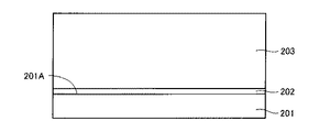
まず、本発明の一実施の形態である実施の形態1について説明する。図1を参照して、本実施の形態における半導体装置(DiMOSFET)であるMOSFET100は、導電型がn型(第1導電型)である炭化珪素基板1と、炭化珪素からなり導電型がn型であるバッファ層2と、炭化珪素からなり導電型がn型のドリフト層3と、導電型がp型(第2導電型)の一対のp型ボディ領域4と、導電型がn型のn+領域5と、導電型がp型のp+領域6とを備えている。
次に、本発明の他の実施の形態である実施の形態2について説明する。実施の形態2における半導体装置であるIGBT200は、炭化珪素基板の面方位およびp型ボディ領域のp型不純物密度に関して上記実施の形態1におけるMOSFET100と同様の構造を有することにより、同様の効果を奏する。

Claims (22)
- {0001}面に対するオフ角が50°以上65°以下である主面を有する炭化珪素基板と、
前記主面上に形成され、導電型が第1導電型であるエピタキシャル成長層と、
前記エピタキシャル成長層上に接触して形成された絶縁膜と、
前記エピタキシャル成長層において前記絶縁膜と接触する領域を含むように形成され、導電型が前記第1導電型とは異なる第2導電型であるボディ領域とを備え、
前記ボディ領域における不純物密度は5×1017cm−3以上であり、
前記ボディ領域の、前記絶縁膜と接触する領域にチャネル領域が形成され、前記エピタキシャル成長層と前記絶縁膜との界面におけるバリアハイトは2.2eV以上2.6eV以下である、半導体装置。 - 前記主面のオフ方位と<01−10>方向とのなす角は5°以下となっている、請求項1に記載の半導体装置。
- 前記主面の、<01−10>方向における{03−38}面に対するオフ角は−3°以上5°以下である、請求項2に記載の半導体装置。
- 前記主面のオフ方位と<−2110>方向とのなす角は5°以下となっている、請求項1に記載の半導体装置。
- 前記主面は、前記炭化珪素基板を構成する炭化珪素のカーボン面側の面である、請求項1から請求項4のいずれか1項に記載の半導体装置。
- 前記ボディ領域における不純物密度は1×1020cm−3以下である、請求項1から請求項5のいずれか1項に記載の半導体装置。
- ノーマリーオフ型となっている、請求項1から請求項6のいずれか1項に記載の半導体装置。
- 前記絶縁膜上に接触して配置されたゲート電極をさらに備え、
前記ゲート電極は前記第2導電型のポリシリコンからなっている、請求項7に記載の半導体装置。 - 前記絶縁膜上に接触して配置されたゲート電極をさらに備え、
前記ゲート電極はn型ポリシリコンからなっている、請求項1から請求項7のいずれか1項に記載の半導体装置。 - 前記絶縁膜の厚みは25nm以上70nm以下である、請求項1から請求項9のいずれか1項に記載の半導体装置。
- 前記第1導電型はn型であり、前記第2導電型はp型である、請求項1から請求項10のいずれか1項に記載の半導体装置。
- 前記ボディ領域における不純物密度は5×1017cm−3以上3×1018cm−3以下である、請求項11に記載の半導体装置。
- 前記ボディ領域において前記絶縁膜に接する領域に弱反転層が形成される閾値電圧が、室温以上100℃以下の温度範囲において2V以上である、請求項11または請求項12に記載の半導体装置。
- 前記閾値電圧が100℃において3V以上である、請求項13に記載の半導体装置。
- 前記閾値電圧が200℃において1V以上である、請求項13または請求項14に記載の半導体装置。
- 前記閾値電圧の温度依存性が−10mV/℃以上である、請求項13から請求項15のいずれか1項に記載の半導体装置。
- 室温における電子のチャネル移動度が30cm2/Vs以上である、請求項11から請求項16のいずれか1項に記載の半導体装置。
- 100℃における電子のチャネル移動度が50cm2/Vs以上である、請求項17に記載の半導体装置。
- 150℃における電子のチャネル移動度が40cm2/Vs以上である、請求項17または請求項18に記載の半導体装置。
- 電子のチャネル移動度の温度依存性が−0.3cm2/Vs℃以上である、請求項17から請求項19のいずれか1項に記載の半導体装置。
- オン状態において、前記ボディ領域に形成されるチャネル領域における抵抗値であるチャネル抵抗は、前記チャネル領域以外の前記エピタキシャル成長層における抵抗値であるドリフト抵抗よりも小さい、請求項1から請求項20のいずれか1項に記載の半導体装置。
- DiMOSFETである、請求項1から請求項21のいずれか1項に記載の半導体装置。
Priority Applications (8)
| Application Number | Priority Date | Filing Date | Title |
|---|---|---|---|
| JP2011012510A JP5699628B2 (ja) | 2010-07-26 | 2011-01-25 | 半導体装置 |
| CN2011800204785A CN103168361A (zh) | 2010-07-26 | 2011-06-29 | 半导体器件 |
| EP11812210.0A EP2600402A4 (en) | 2010-07-26 | 2011-06-29 | SEMICONDUCTOR DEVICE |
| PCT/JP2011/064897 WO2012014617A1 (ja) | 2010-07-26 | 2011-06-29 | 半導体装置 |
| CA2796857A CA2796857A1 (en) | 2010-07-26 | 2011-06-29 | Semiconductor device |
| KR1020127019037A KR20130092377A (ko) | 2010-07-26 | 2011-06-29 | 반도체 장치 |
| TW100126054A TW201210025A (en) | 2010-07-26 | 2011-07-22 | Semiconductor device |
| US13/190,001 US20120018743A1 (en) | 2010-07-26 | 2011-07-25 | Semiconductor device |
Applications Claiming Priority (3)
| Application Number | Priority Date | Filing Date | Title |
|---|---|---|---|
| JP2010167004 | 2010-07-26 | ||
| JP2010167004 | 2010-07-26 | ||
| JP2011012510A JP5699628B2 (ja) | 2010-07-26 | 2011-01-25 | 半導体装置 |
Publications (3)
| Publication Number | Publication Date |
|---|---|
| JP2012049491A JP2012049491A (ja) | 2012-03-08 |
| JP2012049491A5 JP2012049491A5 (ja) | 2014-01-23 |
| JP5699628B2 true JP5699628B2 (ja) | 2015-04-15 |
Family
ID=45492856
Family Applications (1)
| Application Number | Title | Priority Date | Filing Date |
|---|---|---|---|
| JP2011012510A Active JP5699628B2 (ja) | 2010-07-26 | 2011-01-25 | 半導体装置 |
Country Status (8)
| Country | Link |
|---|---|
| US (1) | US20120018743A1 (ja) |
| EP (1) | EP2600402A4 (ja) |
| JP (1) | JP5699628B2 (ja) |
| KR (1) | KR20130092377A (ja) |
| CN (1) | CN103168361A (ja) |
| CA (1) | CA2796857A1 (ja) |
| TW (1) | TW201210025A (ja) |
| WO (1) | WO2012014617A1 (ja) |
Families Citing this family (18)
| Publication number | Priority date | Publication date | Assignee | Title |
|---|---|---|---|---|
| US8674439B2 (en) | 2010-08-02 | 2014-03-18 | Microsemi Corporation | Low loss SiC MOSFET |
| JP5668576B2 (ja) * | 2011-04-01 | 2015-02-12 | 住友電気工業株式会社 | 炭化珪素半導体装置 |
| JP5751113B2 (ja) * | 2011-09-28 | 2015-07-22 | 住友電気工業株式会社 | 炭化珪素半導体装置の製造方法 |
| JP5811829B2 (ja) | 2011-12-22 | 2015-11-11 | 住友電気工業株式会社 | 半導体装置の製造方法 |
| CN102664192B (zh) * | 2012-05-08 | 2015-03-11 | 北京大学 | 一种自适应复合机制隧穿场效应晶体管及其制备方法 |
| JP2014007310A (ja) * | 2012-06-26 | 2014-01-16 | Sumitomo Electric Ind Ltd | 炭化珪素半導体装置の製造方法および炭化珪素半導体装置 |
| JP6068042B2 (ja) * | 2012-08-07 | 2017-01-25 | 住友電気工業株式会社 | 炭化珪素半導体装置およびその製造方法 |
| JP2014038896A (ja) * | 2012-08-13 | 2014-02-27 | Sumitomo Electric Ind Ltd | 炭化珪素半導体装置 |
| JP5646569B2 (ja) | 2012-09-26 | 2014-12-24 | 株式会社東芝 | 半導体装置 |
| WO2014132582A1 (ja) * | 2013-02-28 | 2014-09-04 | 三菱電機株式会社 | 半導体装置 |
| JP2016519428A (ja) * | 2013-03-21 | 2016-06-30 | マイクロセミ コーポレーション | 安全動作領域を拡大したSiCパワー縦型DMOS |
| JP6242633B2 (ja) * | 2013-09-03 | 2017-12-06 | 株式会社東芝 | 半導体装置 |
| DE112014005188T5 (de) * | 2013-11-13 | 2016-07-21 | Mitsubishi Electric Corporation | Verfahren zum Herstellen eines Halbleiterbauteils |
| JP6089015B2 (ja) * | 2014-10-17 | 2017-03-01 | 株式会社東芝 | 半導体装置 |
| CN107331603B (zh) * | 2017-03-20 | 2020-05-01 | 中国电子科技集团公司第五十五研究所 | 一种碳化硅mosfet单胞结构的制造方法 |
| CN108257872A (zh) * | 2018-01-12 | 2018-07-06 | 北京品捷电子科技有限公司 | 一种SiC基DI-MOSFET的制备方法及SiC基DI-MOSFET |
| GB2589543A (en) * | 2019-09-09 | 2021-06-09 | Mqsemi Ag | Method for forming a low injection P-type contact region and power semiconductor devices with the same |
| CN111129155A (zh) * | 2019-12-25 | 2020-05-08 | 重庆伟特森电子科技有限公司 | 一种低栅漏电容碳化硅di-mosfet制备方法 |
Family Cites Families (17)
| Publication number | Priority date | Publication date | Assignee | Title |
|---|---|---|---|---|
| US5877515A (en) * | 1995-10-10 | 1999-03-02 | International Rectifier Corporation | SiC semiconductor device |
| JP2000106428A (ja) * | 1998-09-28 | 2000-04-11 | Toshiba Corp | 半導体装置 |
| JP3854508B2 (ja) * | 1999-09-07 | 2006-12-06 | 株式会社シクスオン | SiCウエハ、SiC半導体デバイス、およびSiCウエハの製造方法 |
| JP4843854B2 (ja) * | 2001-03-05 | 2011-12-21 | 住友電気工業株式会社 | Mosデバイス |
| JP3697211B2 (ja) * | 2002-01-10 | 2005-09-21 | 日本原子力研究所 | 炭化珪素半導体素子及びその絶縁膜の形成方法 |
| US7221010B2 (en) * | 2002-12-20 | 2007-05-22 | Cree, Inc. | Vertical JFET limited silicon carbide power metal-oxide semiconductor field effect transistors |
| JP5368140B2 (ja) * | 2003-03-28 | 2013-12-18 | 三菱電機株式会社 | SiCを用いた縦型MOSFETの製造方法 |
| JP2005167035A (ja) * | 2003-12-03 | 2005-06-23 | Kansai Electric Power Co Inc:The | 炭化珪素半導体素子およびその製造方法 |
| JP4775102B2 (ja) * | 2005-05-09 | 2011-09-21 | 住友電気工業株式会社 | 半導体装置の製造方法 |
| US7727904B2 (en) * | 2005-09-16 | 2010-06-01 | Cree, Inc. | Methods of forming SiC MOSFETs with high inversion layer mobility |
| JPWO2007086196A1 (ja) * | 2006-01-30 | 2009-06-18 | 住友電気工業株式会社 | 炭化珪素半導体装置の製造方法 |
| US20090134476A1 (en) * | 2007-11-13 | 2009-05-28 | Thunderbird Technologies, Inc. | Low temperature coefficient field effect transistors and design and fabrication methods |
| JP5504597B2 (ja) * | 2007-12-11 | 2014-05-28 | 住友電気工業株式会社 | 炭化ケイ素半導体装置およびその製造方法 |
| JP2009272365A (ja) * | 2008-05-01 | 2009-11-19 | Renesas Technology Corp | 半導体装置の製造方法 |
| JP5564781B2 (ja) * | 2008-07-07 | 2014-08-06 | 住友電気工業株式会社 | 炭化ケイ素半導体装置およびその製造方法 |
| CN102150270B (zh) * | 2009-03-27 | 2014-04-09 | 住友电气工业株式会社 | Mosfet和用于制造mosfet的方法 |
| CN105609565B (zh) * | 2009-09-16 | 2019-02-22 | 株式会社半导体能源研究所 | 半导体器件及其制造方法 |
-
2011
- 2011-01-25 JP JP2011012510A patent/JP5699628B2/ja active Active
- 2011-06-29 WO PCT/JP2011/064897 patent/WO2012014617A1/ja active Application Filing
- 2011-06-29 EP EP11812210.0A patent/EP2600402A4/en not_active Withdrawn
- 2011-06-29 KR KR1020127019037A patent/KR20130092377A/ko not_active Application Discontinuation
- 2011-06-29 CA CA2796857A patent/CA2796857A1/en not_active Abandoned
- 2011-06-29 CN CN2011800204785A patent/CN103168361A/zh active Pending
- 2011-07-22 TW TW100126054A patent/TW201210025A/zh unknown
- 2011-07-25 US US13/190,001 patent/US20120018743A1/en not_active Abandoned
Also Published As
| Publication number | Publication date |
|---|---|
| KR20130092377A (ko) | 2013-08-20 |
| EP2600402A1 (en) | 2013-06-05 |
| TW201210025A (en) | 2012-03-01 |
| CA2796857A1 (en) | 2012-02-02 |
| WO2012014617A1 (ja) | 2012-02-02 |
| CN103168361A (zh) | 2013-06-19 |
| EP2600402A4 (en) | 2013-12-25 |
| US20120018743A1 (en) | 2012-01-26 |
| JP2012049491A (ja) | 2012-03-08 |
Similar Documents
| Publication | Publication Date | Title |
|---|---|---|
| JP5699628B2 (ja) | 半導体装置 | |
| JP5668576B2 (ja) | 炭化珪素半導体装置 | |
| US8610131B2 (en) | Silicon carbide insulated-gate bipolar transistor | |
| EP2725622B1 (en) | Silicon carbide semiconductor element and method for producing same | |
| WO2012169224A1 (ja) | 半導体装置 | |
| US8564017B2 (en) | Silicon carbide semiconductor device and method for manufacturing same | |
| WO2010038547A1 (ja) | 炭化珪素半導体装置 | |
| KR20110137279A (ko) | 절연 게이트형 바이폴러 트랜지스터 | |
| KR20140001947A (ko) | 반도체 장치 | |
| JP2015032614A (ja) | 炭化珪素半導体装置およびその製造方法 | |
| JP5870672B2 (ja) | 半導体装置 | |
| JP5655570B2 (ja) | 半導体装置の製造方法 | |
| CN104854704A (zh) | 碳化硅半导体器件 | |
| JP5673113B2 (ja) | 半導体装置 |
Legal Events
| Date | Code | Title | Description |
|---|---|---|---|
| A621 | Written request for application examination |
Free format text: JAPANESE INTERMEDIATE CODE: A621 Effective date: 20130828 |
|
| A521 | Request for written amendment filed |
Free format text: JAPANESE INTERMEDIATE CODE: A523 Effective date: 20131204 |
|
| A131 | Notification of reasons for refusal |
Free format text: JAPANESE INTERMEDIATE CODE: A131 Effective date: 20140527 |
|
| A521 | Request for written amendment filed |
Free format text: JAPANESE INTERMEDIATE CODE: A523 Effective date: 20140702 |
|
| TRDD | Decision of grant or rejection written | ||
| A01 | Written decision to grant a patent or to grant a registration (utility model) |
Free format text: JAPANESE INTERMEDIATE CODE: A01 Effective date: 20150120 |
|
| A61 | First payment of annual fees (during grant procedure) |
Free format text: JAPANESE INTERMEDIATE CODE: A61 Effective date: 20150202 |
|
| R150 | Certificate of patent or registration of utility model |
Ref document number: 5699628 Country of ref document: JP Free format text: JAPANESE INTERMEDIATE CODE: R150 |
|
| R250 | Receipt of annual fees |
Free format text: JAPANESE INTERMEDIATE CODE: R250 |
|
| R250 | Receipt of annual fees |
Free format text: JAPANESE INTERMEDIATE CODE: R250 |
|
| R250 | Receipt of annual fees |
Free format text: JAPANESE INTERMEDIATE CODE: R250 |
|
| R250 | Receipt of annual fees |
Free format text: JAPANESE INTERMEDIATE CODE: R250 |
|
| R250 | Receipt of annual fees |
Free format text: JAPANESE INTERMEDIATE CODE: R250 |
|
| R250 | Receipt of annual fees |
Free format text: JAPANESE INTERMEDIATE CODE: R250 |
|
| R250 | Receipt of annual fees |
Free format text: JAPANESE INTERMEDIATE CODE: R250 |