JP5699628B2 - Semiconductor device - Google Patents
Semiconductor device Download PDFInfo
- Publication number
- JP5699628B2 JP5699628B2 JP2011012510A JP2011012510A JP5699628B2 JP 5699628 B2 JP5699628 B2 JP 5699628B2 JP 2011012510 A JP2011012510 A JP 2011012510A JP 2011012510 A JP2011012510 A JP 2011012510A JP 5699628 B2 JP5699628 B2 JP 5699628B2
- Authority
- JP
- Japan
- Prior art keywords
- semiconductor device
- region
- type
- main surface
- body region
- Prior art date
- Legal status (The legal status is an assumption and is not a legal conclusion. Google has not performed a legal analysis and makes no representation as to the accuracy of the status listed.)
- Active
Links
- 239000004065 semiconductor Substances 0.000 title claims description 100
- 210000000746 body region Anatomy 0.000 claims description 94
- HBMJWWWQQXIZIP-UHFFFAOYSA-N silicon carbide Chemical compound [Si+]#[C-] HBMJWWWQQXIZIP-UHFFFAOYSA-N 0.000 claims description 73
- 229910010271 silicon carbide Inorganic materials 0.000 claims description 73
- 239000012535 impurity Substances 0.000 claims description 64
- 239000000758 substrate Substances 0.000 claims description 62
- 229910021420 polycrystalline silicon Inorganic materials 0.000 claims description 16
- 229920005591 polysilicon Polymers 0.000 claims description 16
- 230000004888 barrier function Effects 0.000 claims description 8
- OKTJSMMVPCPJKN-UHFFFAOYSA-N Carbon Chemical compound [C] OKTJSMMVPCPJKN-UHFFFAOYSA-N 0.000 claims description 7
- 229910052799 carbon Inorganic materials 0.000 claims description 7
- 239000010410 layer Substances 0.000 description 98
- 238000010438 heat treatment Methods 0.000 description 28
- MWUXSHHQAYIFBG-UHFFFAOYSA-N Nitric oxide Chemical compound O=[N] MWUXSHHQAYIFBG-UHFFFAOYSA-N 0.000 description 20
- 238000000034 method Methods 0.000 description 20
- 230000007423 decrease Effects 0.000 description 17
- 238000004519 manufacturing process Methods 0.000 description 17
- 239000000463 material Substances 0.000 description 15
- 238000000137 annealing Methods 0.000 description 14
- VYPSYNLAJGMNEJ-UHFFFAOYSA-N Silicium dioxide Chemical compound O=[Si]=O VYPSYNLAJGMNEJ-UHFFFAOYSA-N 0.000 description 12
- 230000000052 comparative effect Effects 0.000 description 12
- 239000007789 gas Substances 0.000 description 12
- 239000011229 interlayer Substances 0.000 description 12
- 238000005468 ion implantation Methods 0.000 description 12
- 238000002474 experimental method Methods 0.000 description 9
- 229910004298 SiO 2 Inorganic materials 0.000 description 8
- 230000015572 biosynthetic process Effects 0.000 description 8
- 239000004020 conductor Substances 0.000 description 8
- PXHVJJICTQNCMI-UHFFFAOYSA-N nickel Substances [Ni] PXHVJJICTQNCMI-UHFFFAOYSA-N 0.000 description 8
- XKRFYHLGVUSROY-UHFFFAOYSA-N Argon Chemical compound [Ar] XKRFYHLGVUSROY-UHFFFAOYSA-N 0.000 description 6
- XUIMIQQOPSSXEZ-UHFFFAOYSA-N Silicon Chemical compound [Si] XUIMIQQOPSSXEZ-UHFFFAOYSA-N 0.000 description 6
- 229910052782 aluminium Inorganic materials 0.000 description 6
- 239000000969 carrier Substances 0.000 description 6
- 150000002500 ions Chemical class 0.000 description 6
- 229910052710 silicon Inorganic materials 0.000 description 6
- 239000010703 silicon Substances 0.000 description 6
- 235000012239 silicon dioxide Nutrition 0.000 description 6
- 239000000377 silicon dioxide Substances 0.000 description 6
- XAGFODPZIPBFFR-UHFFFAOYSA-N aluminium Chemical compound [Al] XAGFODPZIPBFFR-UHFFFAOYSA-N 0.000 description 5
- 230000008569 process Effects 0.000 description 5
- 229910052796 boron Inorganic materials 0.000 description 4
- 230000015556 catabolic process Effects 0.000 description 4
- 239000012212 insulator Substances 0.000 description 4
- IJGRMHOSHXDMSA-UHFFFAOYSA-N Atomic nitrogen Chemical compound N#N IJGRMHOSHXDMSA-UHFFFAOYSA-N 0.000 description 3
- ZOXJGFHDIHLPTG-UHFFFAOYSA-N Boron Chemical compound [B] ZOXJGFHDIHLPTG-UHFFFAOYSA-N 0.000 description 3
- 238000013459 approach Methods 0.000 description 3
- 229910052786 argon Inorganic materials 0.000 description 3
- QVGXLLKOCUKJST-UHFFFAOYSA-N atomic oxygen Chemical compound [O] QVGXLLKOCUKJST-UHFFFAOYSA-N 0.000 description 3
- 239000011261 inert gas Substances 0.000 description 3
- 229910021334 nickel silicide Inorganic materials 0.000 description 3
- RUFLMLWJRZAWLJ-UHFFFAOYSA-N nickel silicide Chemical compound [Ni]=[Si]=[Ni] RUFLMLWJRZAWLJ-UHFFFAOYSA-N 0.000 description 3
- 239000001301 oxygen Substances 0.000 description 3
- 229910052760 oxygen Inorganic materials 0.000 description 3
- 229910052698 phosphorus Inorganic materials 0.000 description 3
- 230000009467 reduction Effects 0.000 description 3
- 238000007740 vapor deposition Methods 0.000 description 3
- OAICVXFJPJFONN-UHFFFAOYSA-N Phosphorus Chemical compound [P] OAICVXFJPJFONN-UHFFFAOYSA-N 0.000 description 2
- 230000004913 activation Effects 0.000 description 2
- 239000013078 crystal Substances 0.000 description 2
- 230000006866 deterioration Effects 0.000 description 2
- 238000005530 etching Methods 0.000 description 2
- 230000006872 improvement Effects 0.000 description 2
- 238000005259 measurement Methods 0.000 description 2
- 229910052759 nickel Inorganic materials 0.000 description 2
- 125000004433 nitrogen atom Chemical group N* 0.000 description 2
- 239000011574 phosphorus Substances 0.000 description 2
- 238000000206 photolithography Methods 0.000 description 2
- 238000002360 preparation method Methods 0.000 description 2
- 238000012545 processing Methods 0.000 description 2
- 125000004429 atom Chemical group 0.000 description 1
- 230000008901 benefit Effects 0.000 description 1
- 125000004432 carbon atom Chemical group C* 0.000 description 1
- 229910001873 dinitrogen Inorganic materials 0.000 description 1
- 239000002019 doping agent Substances 0.000 description 1
- 230000000694 effects Effects 0.000 description 1
- 238000001803 electron scattering Methods 0.000 description 1
- 238000001704 evaporation Methods 0.000 description 1
- 230000005669 field effect Effects 0.000 description 1
- 238000011835 investigation Methods 0.000 description 1
- 230000008018 melting Effects 0.000 description 1
- 238000002844 melting Methods 0.000 description 1
- 229910052751 metal Inorganic materials 0.000 description 1
- 239000002184 metal Substances 0.000 description 1
- 229910044991 metal oxide Inorganic materials 0.000 description 1
- 150000004706 metal oxides Chemical class 0.000 description 1
- 238000012986 modification Methods 0.000 description 1
- 230000004048 modification Effects 0.000 description 1
- 229910021421 monocrystalline silicon Inorganic materials 0.000 description 1
- 229910052757 nitrogen Inorganic materials 0.000 description 1
Images


Classifications
-
- H—ELECTRICITY
- H01—ELECTRIC ELEMENTS
- H01L—SEMICONDUCTOR DEVICES NOT COVERED BY CLASS H10
- H01L29/00—Semiconductor devices adapted for rectifying, amplifying, oscillating or switching, or capacitors or resistors with at least one potential-jump barrier or surface barrier, e.g. PN junction depletion layer or carrier concentration layer; Details of semiconductor bodies or of electrodes thereof ; Multistep manufacturing processes therefor
- H01L29/66—Types of semiconductor device ; Multistep manufacturing processes therefor
- H01L29/68—Types of semiconductor device ; Multistep manufacturing processes therefor controllable by only the electric current supplied, or only the electric potential applied, to an electrode which does not carry the current to be rectified, amplified or switched
- H01L29/76—Unipolar devices, e.g. field effect transistors
- H01L29/772—Field effect transistors
- H01L29/78—Field effect transistors with field effect produced by an insulated gate
- H01L29/7801—DMOS transistors, i.e. MISFETs with a channel accommodating body or base region adjoining a drain drift region
- H01L29/7802—Vertical DMOS transistors, i.e. VDMOS transistors
-
- H—ELECTRICITY
- H01—ELECTRIC ELEMENTS
- H01L—SEMICONDUCTOR DEVICES NOT COVERED BY CLASS H10
- H01L21/00—Processes or apparatus adapted for the manufacture or treatment of semiconductor or solid state devices or of parts thereof
- H01L21/02—Manufacture or treatment of semiconductor devices or of parts thereof
- H01L21/04—Manufacture or treatment of semiconductor devices or of parts thereof the devices having at least one potential-jump barrier or surface barrier, e.g. PN junction, depletion layer or carrier concentration layer
- H01L21/0445—Manufacture or treatment of semiconductor devices or of parts thereof the devices having at least one potential-jump barrier or surface barrier, e.g. PN junction, depletion layer or carrier concentration layer the devices having semiconductor bodies comprising crystalline silicon carbide
- H01L21/048—Making electrodes
- H01L21/049—Conductor-insulator-semiconductor electrodes, e.g. MIS contacts
-
- H—ELECTRICITY
- H01—ELECTRIC ELEMENTS
- H01L—SEMICONDUCTOR DEVICES NOT COVERED BY CLASS H10
- H01L29/00—Semiconductor devices adapted for rectifying, amplifying, oscillating or switching, or capacitors or resistors with at least one potential-jump barrier or surface barrier, e.g. PN junction depletion layer or carrier concentration layer; Details of semiconductor bodies or of electrodes thereof ; Multistep manufacturing processes therefor
- H01L29/02—Semiconductor bodies ; Multistep manufacturing processes therefor
- H01L29/04—Semiconductor bodies ; Multistep manufacturing processes therefor characterised by their crystalline structure, e.g. polycrystalline, cubic or particular orientation of crystalline planes
- H01L29/045—Semiconductor bodies ; Multistep manufacturing processes therefor characterised by their crystalline structure, e.g. polycrystalline, cubic or particular orientation of crystalline planes by their particular orientation of crystalline planes
-
- H—ELECTRICITY
- H01—ELECTRIC ELEMENTS
- H01L—SEMICONDUCTOR DEVICES NOT COVERED BY CLASS H10
- H01L29/00—Semiconductor devices adapted for rectifying, amplifying, oscillating or switching, or capacitors or resistors with at least one potential-jump barrier or surface barrier, e.g. PN junction depletion layer or carrier concentration layer; Details of semiconductor bodies or of electrodes thereof ; Multistep manufacturing processes therefor
- H01L29/02—Semiconductor bodies ; Multistep manufacturing processes therefor
- H01L29/06—Semiconductor bodies ; Multistep manufacturing processes therefor characterised by their shape; characterised by the shapes, relative sizes, or dispositions of the semiconductor regions ; characterised by the concentration or distribution of impurities within semiconductor regions
- H01L29/10—Semiconductor bodies ; Multistep manufacturing processes therefor characterised by their shape; characterised by the shapes, relative sizes, or dispositions of the semiconductor regions ; characterised by the concentration or distribution of impurities within semiconductor regions with semiconductor regions connected to an electrode not carrying current to be rectified, amplified or switched and such electrode being part of a semiconductor device which comprises three or more electrodes
- H01L29/1095—Body region, i.e. base region, of DMOS transistors or IGBTs
-
- H—ELECTRICITY
- H01—ELECTRIC ELEMENTS
- H01L—SEMICONDUCTOR DEVICES NOT COVERED BY CLASS H10
- H01L29/00—Semiconductor devices adapted for rectifying, amplifying, oscillating or switching, or capacitors or resistors with at least one potential-jump barrier or surface barrier, e.g. PN junction depletion layer or carrier concentration layer; Details of semiconductor bodies or of electrodes thereof ; Multistep manufacturing processes therefor
- H01L29/66—Types of semiconductor device ; Multistep manufacturing processes therefor
- H01L29/66007—Multistep manufacturing processes
- H01L29/66053—Multistep manufacturing processes of devices having a semiconductor body comprising crystalline silicon carbide
- H01L29/66068—Multistep manufacturing processes of devices having a semiconductor body comprising crystalline silicon carbide the devices being controllable only by the electric current supplied or the electric potential applied, to an electrode which does not carry the current to be rectified, amplified or switched, e.g. three-terminal devices
-
- H—ELECTRICITY
- H01—ELECTRIC ELEMENTS
- H01L—SEMICONDUCTOR DEVICES NOT COVERED BY CLASS H10
- H01L29/00—Semiconductor devices adapted for rectifying, amplifying, oscillating or switching, or capacitors or resistors with at least one potential-jump barrier or surface barrier, e.g. PN junction depletion layer or carrier concentration layer; Details of semiconductor bodies or of electrodes thereof ; Multistep manufacturing processes therefor
- H01L29/66—Types of semiconductor device ; Multistep manufacturing processes therefor
- H01L29/68—Types of semiconductor device ; Multistep manufacturing processes therefor controllable by only the electric current supplied, or only the electric potential applied, to an electrode which does not carry the current to be rectified, amplified or switched
- H01L29/70—Bipolar devices
- H01L29/72—Transistor-type devices, i.e. able to continuously respond to applied control signals
- H01L29/739—Transistor-type devices, i.e. able to continuously respond to applied control signals controlled by field-effect, e.g. bipolar static induction transistors [BSIT]
- H01L29/7393—Insulated gate bipolar mode transistors, i.e. IGBT; IGT; COMFET
- H01L29/7395—Vertical transistors, e.g. vertical IGBT
-
- H—ELECTRICITY
- H01—ELECTRIC ELEMENTS
- H01L—SEMICONDUCTOR DEVICES NOT COVERED BY CLASS H10
- H01L29/00—Semiconductor devices adapted for rectifying, amplifying, oscillating or switching, or capacitors or resistors with at least one potential-jump barrier or surface barrier, e.g. PN junction depletion layer or carrier concentration layer; Details of semiconductor bodies or of electrodes thereof ; Multistep manufacturing processes therefor
- H01L29/02—Semiconductor bodies ; Multistep manufacturing processes therefor
- H01L29/12—Semiconductor bodies ; Multistep manufacturing processes therefor characterised by the materials of which they are formed
- H01L29/16—Semiconductor bodies ; Multistep manufacturing processes therefor characterised by the materials of which they are formed including, apart from doping materials or other impurities, only elements of Group IV of the Periodic System
- H01L29/1608—Silicon carbide
Description
本発明は半導体装置に関し、より特定的には、チャネル移動度の低下を抑制しつつ閾値電圧の設定の自由度を高めることが可能な半導体装置に関するものである。 The present invention relates to a semiconductor device, and more particularly to a semiconductor device capable of increasing the degree of freedom in setting a threshold voltage while suppressing a decrease in channel mobility.
近年、半導体装置の高耐圧化、低損失化、高温環境下での使用などを可能とするため、半導体装置を構成する材料として炭化珪素の採用が進められつつある。炭化珪素は、従来から半導体装置を構成する材料として広く使用されている珪素に比べてバンドギャップが大きいワイドバンドギャップ半導体である。そのため、半導体装置を構成する材料として炭化珪素を採用することにより、半導体装置の高耐圧化、オン抵抗の低減などを達成することができる。また、炭化珪素を材料として採用した半導体装置は、珪素を材料として採用した半導体装置に比べて、高温環境下で使用された場合の特性の低下が小さいという利点も有している。 In recent years, in order to enable a semiconductor device to have a high breakdown voltage, low loss, use under a high temperature environment, etc., silicon carbide is being adopted as a material constituting the semiconductor device. Silicon carbide is a wide band gap semiconductor having a larger band gap than silicon that has been widely used as a material for forming semiconductor devices. Therefore, by adopting silicon carbide as a material constituting the semiconductor device, it is possible to achieve a high breakdown voltage and a low on-resistance of the semiconductor device. In addition, a semiconductor device that employs silicon carbide as a material has an advantage that a decrease in characteristics when used in a high temperature environment is small as compared with a semiconductor device that employs silicon as a material.
このような炭化珪素を材料として用いた半導体装置のうち、たとえばMOSFET(Metal Oxide Semiconductor Field Effect Transistor)やIGBT(Insulated Gate Bipolar Transistor)など、所定の閾値電圧を境にチャネル領域における反転層の形成の有無をコントロールし、電流を導通および遮断する半導体装置においては、閾値電圧の調整やチャネル移動度の向上について様々な検討がなされている(たとえば非特許文献1参照)。 Among semiconductor devices using such silicon carbide as a material, for example, formation of an inversion layer in a channel region with a predetermined threshold voltage as a boundary, such as a MOSFET (Metal Oxide Field Effect Transistor) or an IGBT (Insulated Gate Bipolar Transistor) In a semiconductor device that controls presence / absence and conducts and cuts off current, various studies have been made on adjustment of threshold voltage and improvement of channel mobility (for example, see Non-Patent Document 1).
ここで、たとえばNチャネルのMOSFETやIGBTなどの半導体装置においては、導電型がp型であるp型ボディ領域が形成され、当該p型ボディ領域内にチャネル領域が形成される。そして、p型ボディ領域におけるp型不純物(たとえばB(硼素)、Al(アルミニウム)など)の密度(ドーピング密度)を高くすることにより、閾値電圧をプラス側にシフトさせ、ノーマリーオフ型に近づける、あるいはノーマリーオフ型とすることができる。一方、Pチャネルの半導体装置においては、上記Nチャネルの場合とは逆にn型ボディ領域におけるn型不純物の密度を高くすることにより、閾値電圧をマイナス側にシフトさせ、ノーマリーオフ型に近づける、あるいはノーマリーオフ型とすることができる。 Here, for example, in a semiconductor device such as an N-channel MOSFET or IGBT, a p-type body region having a p-type conductivity is formed, and a channel region is formed in the p-type body region. Then, by increasing the density (doping density) of p-type impurities (for example, B (boron), Al (aluminum), etc.) in the p-type body region, the threshold voltage is shifted to the plus side to approach the normally-off type. Or a normally-off type. On the other hand, in the P-channel semiconductor device, the density of the n-type impurity in the n-type body region is increased contrary to the case of the N-channel, so that the threshold voltage is shifted to the minus side and becomes close to the normally-off type. Or a normally-off type.
しかし、このような方法で閾値電圧を調整すると、チャネル移動度が大幅に低下するという問題がある。これは、ドーピング密度を高くすることにより、ドーパントによる電子の散乱が顕著になるためである。そのため、たとえばp型ボディ領域のドーピング密度は、たとえば1×1016cm−3〜4×1016cm−3程度とされる。その結果、従来の半導体装置においては、十分なチャネル移動度を確保しつつ閾値電圧を自由に設定すること、特にノーマリーオフ型に近づける、あるいはノーマリーオフ型とすることは難しいという問題があった。 However, when the threshold voltage is adjusted by such a method, there is a problem that the channel mobility is greatly reduced. This is because electron scattering due to the dopant becomes significant by increasing the doping density. Therefore, for example, the p-type body region has a doping density of, for example, about 1 × 10 16 cm −3 to 4 × 10 16 cm −3 . As a result, the conventional semiconductor device has a problem that it is difficult to freely set the threshold voltage while ensuring sufficient channel mobility, in particular, to approach the normally-off type or to be the normally-off type. It was.
本発明はこのような問題に対応するためになされたものであって、その目的は、チャネル移動度の低下を抑制しつつ閾値電圧の設定の自由度を高めることが可能な半導体装置を提供することである。 The present invention has been made to address such problems, and an object of the present invention is to provide a semiconductor device capable of increasing the degree of freedom in setting a threshold voltage while suppressing a decrease in channel mobility. That is.
本発明に従った半導体装置は、{0001}面に対するオフ角が50°以上65°以下である主面を有する炭化珪素基板と、当該主面上に形成され、導電型が第1導電型であるエピタキシャル成長層と、エピタキシャル成長層上に接触して形成された絶縁膜と、エピタキシャル成長層において絶縁膜と接触する領域を含むように形成され、導電型が第1導電型とは異なる第2導電型であるボディ領域とを備えている。そして、ボディ領域における不純物密度は5×10 17 cm−3以上であり、ボディ領域の、絶縁膜と接触する領域にチャネル領域が形成される。 A semiconductor device according to the present invention includes a silicon carbide substrate having a main surface with an off angle of 50 ° or more and 65 ° or less with respect to the {0001} plane, the first conductivity type being formed on the main surface. An epitaxial growth layer, an insulating film formed in contact with the epitaxial growth layer, and a region in contact with the insulating film in the epitaxial growth layer are formed, and the second conductivity type is different from the first conductivity type. With a body area. The impurity concentration in the body region Ri der 5 × 10 17 cm -3 or more, of the body region, Ru channel region is formed in a region in contact with the insulating film.
本発明者は、チャネル移動度の低下を抑制しつつ閾値電圧の設定の自由度を高める方策について詳細な検討を行なった結果、以下のような知見を得て本発明に想到した。従来の炭化珪素を素材として採用した半導体装置においては、炭化珪素基板として{0001}面に対するオフ角が8°以下程度の主面を有する炭化珪素基板が採用される。そして、当該主面上にエピタキシャル成長層等が形成されて半導体装置が作製される。このような半導体装置においては、上述のように十分なチャネル移動度を確保しつつ閾値電圧を自由に設定することは困難である。しかし、本発明者の検討によれば、炭化珪素基板の主面における{0001}面に対するオフ角を所定の範囲とした場合、ボディ領域のドーピング密度上昇とチャネル移動度の向上との相反関係が大幅に緩和されることが明らかとなった。より具体的には、炭化珪素基板として{0001}面に対するオフ角が50°以上65°以下である主面を有する炭化珪素基板を採用し、当該主面上にエピタキシャル成長層を形成した構造において、このエピタキシャル成長層に不純物(たとえばp型不純物であるB、Alなど)を導入してボディ領域を形成した場合、ボディ領域のドーピング密度を上昇させてもチャネル移動度の低下が大幅に抑制される。 As a result of detailed investigations on measures for increasing the degree of freedom in setting the threshold voltage while suppressing a decrease in channel mobility, the present inventor has obtained the following knowledge and arrived at the present invention. In a conventional semiconductor device employing silicon carbide as a material, a silicon carbide substrate having a main surface with an off angle of about 8 ° or less with respect to the {0001} plane is employed as the silicon carbide substrate. And an epitaxial growth layer etc. are formed on the said main surface, and a semiconductor device is produced. In such a semiconductor device, it is difficult to freely set the threshold voltage while ensuring sufficient channel mobility as described above. However, according to the study by the present inventor, when the off angle with respect to the {0001} plane in the main surface of the silicon carbide substrate is set within a predetermined range, there is a conflicting relationship between the increase in doping density of the body region and the improvement in channel mobility It became clear that it was greatly eased. More specifically, in a structure in which a silicon carbide substrate having a main surface with an off angle of 50 ° or more and 65 ° or less with respect to the {0001} plane is employed as a silicon carbide substrate, and an epitaxial growth layer is formed on the main surface, When a body region is formed by introducing impurities (for example, p-type impurities such as B and Al) into this epitaxial growth layer, a decrease in channel mobility is greatly suppressed even if the doping density of the body region is increased.
本発明の半導体装置においては、{0001}面に対するオフ角が50°以上65°以下である主面を有する炭化珪素基板が採用され、当該主面上に形成されたエピタキシャル成長層内にボディ領域が形成される。そのため、不純物密度が5×10 17 cm−3以上という高いドーピング密度のボディ領域を形成し、閾値電圧をプラス側にシフトさせた場合でも、チャネル移動度の低下が抑制される。その結果、本発明の半導体装置によれば、チャネル移動度の低下を抑制しつつ閾値電圧の設定の自由度を高めることが可能な半導体装置を提供することができる。なお、上述の「不純物」は、炭化珪素中に導入されることにより多数キャリアを生成する不純物を意味する。 In the semiconductor device of the present invention, a silicon carbide substrate having a main surface with an off angle of 50 ° or more and 65 ° or less with respect to the {0001} plane is employed, and a body region is formed in the epitaxial growth layer formed on the main surface. It is formed. Therefore, even when a body region having a high doping density of 5 × 10 17 cm −3 or more is formed and the threshold voltage is shifted to the positive side, a decrease in channel mobility is suppressed. As a result, according to the semiconductor device of the present invention, it is possible to provide a semiconductor device capable of increasing the degree of freedom in setting a threshold voltage while suppressing a decrease in channel mobility. The above-mentioned “impurity” means an impurity that generates majority carriers when introduced into silicon carbide.
上記半導体装置においては、上記主面のオフ方位と<01−10>方向とのなす角は5°以下となっていてもよい。 In the semiconductor device, an angle formed between the off orientation of the main surface and the <01-10> direction may be 5 ° or less.
<01−10>方向は、炭化珪素基板における代表的なオフ方位である。そして、基板の製造工程におけるスライス加工のばらつき等に起因したオフ方位のばらつきを5°以下とすることにより、炭化珪素基板上へのエピタキシャル成長層の形成などを容易にすることができる。 The <01-10> direction is a typical off orientation in the silicon carbide substrate. Then, by setting the variation in off orientation due to the variation in slicing in the substrate manufacturing process to 5 ° or less, the formation of an epitaxially grown layer on the silicon carbide substrate can be facilitated.
上記半導体装置においては、上記主面の、<01−10>方向における{03−38}面に対するオフ角は−3°以上5°以下であってもよい。 In the semiconductor device, an off angle of the main surface with respect to the {03-38} plane in the <01-10> direction may be not less than −3 ° and not more than 5 °.
これにより、チャネル移動度を一層向上させることができる。ここで、面方位{03−38}に対するオフ角を−3°以上+5°以下としたのは、チャネル移動度と上記オフ角との関係を調査した結果、この範囲内で特に高いチャネル移動度が得られたことに基づいている。 Thereby, channel mobility can be further improved. Here, the off angle with respect to the plane orientation {03-38} is set to −3 ° or more and + 5 ° or less as a result of investigating the relationship between the channel mobility and the off angle, and the channel mobility is particularly high within this range. Is based on the obtained.
また、「<01−10>方向における{03−38}面に対するオフ角」とは、<01−10>方向および<0001>方向を含む平面への上記主面の法線の正射影と、{03−38}面の法線とのなす角度であり、その符号は、上記正射影が<01−10>方向に対して平行に近づく場合が正であり、上記正射影が<0001>方向に対して平行に近づく場合が負である。 The “off angle with respect to the {03-38} plane in the <01-10> direction” is an orthogonal projection of the normal of the main surface to a plane including the <01-10> direction and the <0001> direction. It is an angle formed with the normal of the {03-38} plane, and its sign is positive when the orthographic projection approaches parallel to the <01-10> direction, and the orthographic projection is in the <0001> direction. The case of approaching parallel to is negative.
なお、上記主面の面方位は、実質的に{03−38}であることがより好ましく、上記主面の面方位は{03−38}であることがさらに好ましい。ここで、主面の面方位が実質的に{03−38}であるとは、基板の加工精度などを考慮して実質的に面方位が{03−38}とみなせるオフ角の範囲に基板の主面の面方位が含まれていることを意味し、この場合のオフ角の範囲はたとえば{03−38}に対してオフ角が±2°の範囲である。これにより、上述したチャネル移動度をより一層向上させることができる。 In addition, it is more preferable that the surface orientation of the main surface is substantially {03-38}, and it is further preferable that the surface orientation of the main surface is {03-38}. Here, the surface orientation of the main surface is substantially {03-38}, taking into account the processing accuracy of the substrate, etc., the substrate is within the range of the off angle where the surface orientation can be substantially regarded as {03-38}. In this case, the off-angle range is, for example, a range where the off-angle is ± 2 ° with respect to {03-38}. As a result, the above-described channel mobility can be further improved.
上記半導体装置においては、上記主面のオフ方位と<−2110>方向とのなす角は5°以下となっていてもよい。 In the semiconductor device, an angle formed between the off orientation of the main surface and the <-2110> direction may be 5 ° or less.
<−2110>方向は、上記<01−10>方向と同様に、炭化珪素基板における代表的なオフ方位である。そして、基板の製造工程におけるスライス加工のばらつき等に起因したオフ方位のばらつきを±5°とすることにより、炭化珪素基板上へのエピタキシャル成長層の形成などを容易にすることができる。 The <-2110> direction is a typical off orientation in the silicon carbide substrate, similarly to the <01-10> direction. Then, by setting the variation in off orientation due to the variation in slicing in the manufacturing process of the substrate to ± 5 °, formation of an epitaxially grown layer on the silicon carbide substrate can be facilitated.
上記半導体装置においては、上記主面は、炭化珪素基板を構成する炭化珪素のカーボン面側の面であってもよい。 In the semiconductor device, the main surface may be a surface on the carbon surface side of silicon carbide constituting the silicon carbide substrate.
このようにすることにより、チャネル移動度をさらに向上させることができる。ここで、六方晶の単結晶炭化珪素の(0001)面はシリコン面、(000−1)面はカーボン面と定義される。つまり、上記主面のオフ方位と<01−10>方向とのなす角が5°以下である構成を採用する場合、上記主面を(0−33−8)面に近いものとすることにより、チャネル移動度をさらに向上させることができる。 By doing so, the channel mobility can be further improved. Here, the (0001) plane of hexagonal single crystal silicon carbide is defined as the silicon plane, and the (000-1) plane is defined as the carbon plane. That is, by adopting a configuration in which the angle between the off orientation of the main surface and the <01-10> direction is 5 ° or less, the main surface is made close to the (0-33-8) plane. The channel mobility can be further improved.
上記半導体装置においては、上記ボディ領域における不純物密度は1×1020cm−3以下であってもよい。 In the semiconductor device, the impurity density in the body region may be 1 × 10 20 cm −3 or less.
ボディ領域における不純物密度を1×1020cm−3以下としても、閾値電圧は十分な自由度をもって設定することができる。また、1×1020cm−3を超えるドーピング密度を採用すると、結晶性の悪化などの問題が発生する可能性がある。 Even if the impurity density in the body region is 1 × 10 20 cm −3 or less, the threshold voltage can be set with a sufficient degree of freedom. Further, when a doping density exceeding 1 × 10 20 cm −3 is employed, problems such as deterioration of crystallinity may occur.
上記半導体装置は、ノーマリーオフ型となっていてもよい。このようにノーマリーオフ型になる程度にボディ領域のドーピング密度を高くした場合でも、本発明の半導体装置によればチャネル移動度の低下を十分に抑制することができる。 The semiconductor device may be a normally-off type. Thus, even when the doping density of the body region is increased to such an extent that it is normally off, according to the semiconductor device of the present invention, the decrease in channel mobility can be sufficiently suppressed.
上記半導体装置においては、上記絶縁膜上に接触して配置されたゲート電極をさらに備え、当該ゲート電極は第2導電型のポリシリコンからなっていてもよい。すなわち、第2導電型がp型である場合、ゲート電極はp型ポリシリコンからなるものとし、第2導電型がn型である場合、ゲート電極はn型ポリシリコンからなるものとすることができる。p型ポリシリコンとは、多数キャリアが正孔であるポリシリコンをいい、n型ポリシリコンとは、多数キャリアが電子であるポリシリコンをいう。このようにすることにより、半導体装置をノーマリーオフ型とすることが容易となる。 The semiconductor device may further include a gate electrode disposed in contact with the insulating film, and the gate electrode may be made of second conductivity type polysilicon. That is, when the second conductivity type is p-type, the gate electrode is made of p-type polysilicon, and when the second conductivity type is n-type, the gate electrode is made of n-type polysilicon. it can. P-type polysilicon refers to polysilicon whose majority carriers are holes, and n-type polysilicon refers to polysilicon whose majority carriers are electrons. By doing so, it becomes easy to make the semiconductor device normally-off type.
上記半導体装置においては、絶縁膜上に接触して配置されたゲート電極をさらに備え、当該ゲート電極はn型ポリシリコンからなっていてもよい。このようにすることにより、半導体装置のスイッチング速度を向上させることができる。 The semiconductor device may further include a gate electrode disposed in contact with the insulating film, and the gate electrode may be made of n-type polysilicon. By doing so, the switching speed of the semiconductor device can be improved.
上記半導体装置においては、上記絶縁膜の厚みは25nm以上70nm以下であってもよい。上記絶縁膜の厚みが25nm未満では、動作中に絶縁破壊が発生するおそれがある。一方、上記絶縁膜の厚みが70nmを超える場合、当該絶縁膜をゲート絶縁膜として使用する場合のゲート電圧の絶対値を大きくする必要が生じる。そのため、上記絶縁膜の厚みを25nm以上70nm以下とすることにより、上記問題点を容易に解消することができる。 In the semiconductor device, the insulating film may have a thickness of 25 nm to 70 nm. If the thickness of the insulating film is less than 25 nm, dielectric breakdown may occur during operation. On the other hand, when the thickness of the insulating film exceeds 70 nm, it is necessary to increase the absolute value of the gate voltage when the insulating film is used as a gate insulating film. Therefore, the above problem can be easily solved by setting the thickness of the insulating film to 25 nm or more and 70 nm or less.
上記半導体装置においては、上記第1導電型はn型であり、第2導電型はp型であってもよい。すなわち、上記半導体装置は、Nチャネル型であってもよい。このようにすることにより、高い移動度を確保することが容易な電子を多数キャリアとする半導体装置を提供することができる。 In the semiconductor device, the first conductivity type may be n-type and the second conductivity type may be p-type. That is, the semiconductor device may be an N channel type. By doing so, it is possible to provide a semiconductor device using electrons as majority carriers, which can easily ensure high mobility.
上記半導体装置においては、ボディ領域における不純物密度は5×10 17 cm−3以上3×1018cm−3以下であってもよい。このようにすることにより、本願の半導体装置を、珪素を材料として採用した半導体装置と置き換えて使用することが容易になるとともに、半導体装置を安定してノーマリーオフ型とすることができる。また、不純物密度が高くなることによる大幅なチャネル移動度の低下を回避することができる。 In the semiconductor device, the impurity density in the body region may be 5 × 10 17 cm −3 or more and 3 × 10 18 cm −3 or less. In this way, the semiconductor device of the present patent application, silicon with is easy to use by replacing a semiconductor device employing as the material can be a normally-off-type semiconductor device stable. In addition, a significant reduction in channel mobility due to an increase in impurity density can be avoided.
上記半導体装置においては、ボディ領域において絶縁膜に接する領域に弱反転層が形成される閾値電圧は、室温以上100℃以下の温度範囲において2V以上であってもよい。これにより、通常の動作温度においてより確実にノーマリーオフの状態を維持することができる。ここで、室温とは具体的には27℃である。 In the semiconductor device, the threshold voltage at which the weak inversion layer is formed in a region in contact with the insulating film in the body region may be 2 V or more in a temperature range of room temperature to 100 ° C. As a result, the normally-off state can be more reliably maintained at the normal operating temperature. Here, the room temperature is specifically 27 ° C.
上記半導体装置においては、上記閾値電圧が100℃において3V以上であってもよい。これにより、動作温度が高温である場合でも、より確実にノーマリーオフの状態を維持することができる。 In the semiconductor device, the threshold voltage may be 3 V or more at 100 ° C. Thereby, even when the operating temperature is high, the normally-off state can be more reliably maintained.
上記半導体装置においては、上記閾値電圧が200℃において1V以上であってもよい。これにより、動作温度がより高温である場合でも、より確実にノーマリーオフの状態を維持することができる。 In the semiconductor device, the threshold voltage may be 1 V or more at 200 ° C. Thereby, even when the operating temperature is higher, the normally-off state can be more reliably maintained.
上記半導体装置においては、上記閾値電圧の温度依存性は−10mV/℃以上であってもよい。このようにすることにより、安定してノーマリーオフの状態を維持することができる。 In the semiconductor device, the temperature dependence of the threshold voltage may be −10 mV / ° C. or higher. By doing so, the normally-off state can be stably maintained.
上記半導体装置においては、室温における電子のチャネル移動度が30cm2/Vs以上であってもよい。このようにすることにより、半導体装置のオン抵抗を十分に抑制することが容易となる。 In the semiconductor device, the channel mobility of electrons at room temperature may be 30 cm 2 / Vs or higher. By doing so, it becomes easy to sufficiently suppress the on-resistance of the semiconductor device.
上記半導体装置においては、100℃における電子のチャネル移動度が50cm2/Vs以上であってもよい。これにより、動作温度が高温である場合でも、半導体装置のオン抵抗を十分に抑制することが可能となる。 In the semiconductor device, the channel mobility of electrons at 100 ° C. may be 50 cm 2 / Vs or more. Thereby, even when the operating temperature is high, the on-resistance of the semiconductor device can be sufficiently suppressed.
上記半導体装置においては、150℃における電子のチャネル移動度が40cm2/Vs以上であってもよい。これにより、動作温度がより高温である場合でも、半導体装置のオン抵抗を十分に抑制することが可能となる。 In the above semiconductor device, the channel mobility of electrons at 150 ° C. may be 40 cm 2 / Vs or more. Thereby, even when the operating temperature is higher, the on-resistance of the semiconductor device can be sufficiently suppressed.
上記半導体装置においては、電子のチャネル移動度の温度依存性が−0.3cm2/Vs℃以上であってもよい。これにより、安定して半導体装置のオン抵抗を抑制することが可能となる。 In the semiconductor device, the temperature dependence of the electron channel mobility may be −0.3 cm 2 / Vs ° C. or more. As a result, the on-resistance of the semiconductor device can be stably suppressed.
上記半導体装置においては、エピタキシャル成長層と絶縁膜との界面におけるバリアハイトは2.2eV以上2.6eV以下であってもよい。 In the above semiconductor device, the barrier height at the interface between the epitaxial growth layer and the insulating film may be 2.2 eV or more and 2.6 eV or less.
バリアハイトを大きくすることにより、ゲート絶縁膜として機能する上記絶縁膜中を流れるリーク電流(トンネル電流)を抑制することができる。しかし、上記エピタキシャル成長層が炭化珪素からなる場合、単に絶縁膜との間のバリアハイトが大きい結晶面を絶縁膜と接触する面に採用すると、チャネル移動度が低下するという問題が生じる。これに対し、バリアハイトが2.2eV以上2.6eVとなる結晶面を絶縁膜と接触する面に採用することにより、リーク電流を抑制しつつ、高いチャネル移動度を確保することができる。このようなバリアハイトは、{0001}面に対するオフ角が50°以上65°以下である主面を有する炭化珪素基板を採用することにより、容易に達成することができる。なお、バリアハイトとは、エピタキシャル成長層の伝導帯と絶縁膜の伝導帯との間のバンドギャップの大きさをいう。 By increasing the barrier height, leakage current (tunnel current) flowing through the insulating film functioning as a gate insulating film can be suppressed. However, when the epitaxial growth layer is made of silicon carbide, if a crystal plane having a large barrier height with the insulating film is simply used as the surface in contact with the insulating film, there arises a problem that the channel mobility is lowered. On the other hand, by adopting a crystal surface having a barrier height of 2.2 eV or more and 2.6 eV as a surface in contact with the insulating film, high channel mobility can be secured while suppressing leakage current. Such a barrier height can be easily achieved by employing a silicon carbide substrate having a main surface with an off angle of 50 ° or more and 65 ° or less with respect to the {0001} plane. The barrier height refers to the size of the band gap between the conduction band of the epitaxial growth layer and the conduction band of the insulating film.
上記半導体装置においては、オン状態において、ボディ領域に形成されるチャネル領域における抵抗値であるチャネル抵抗は、チャネル領域以外のエピタキシャル成長層における抵抗値であるドリフト抵抗よりも小さくなっていてもよい。これにより、半導体装置のオン抵抗を低減することができる。このようなチャネル抵抗とドリフト抵抗との関係は、{0001}面に対するオフ角が50°以上65°以下である主面を有する炭化珪素基板を採用することにより、容易に達成することができる。 In the semiconductor device, in the ON state, the channel resistance that is the resistance value in the channel region formed in the body region may be smaller than the drift resistance that is the resistance value in the epitaxial growth layer other than the channel region. Thereby, the on-resistance of the semiconductor device can be reduced. Such a relationship between channel resistance and drift resistance can be easily achieved by employing a silicon carbide substrate having a main surface with an off angle of 50 ° or more and 65 ° or less with respect to the {0001} plane.
上記半導体装置は、DiMOSFET(Double Implanted MOSFET)であってもよい。本発明の半導体装置は、比較的構造がシンプルなDiMOSFETに対しても、好適である。 The semiconductor device may be a DiMOSFET (Double Implanted MOSFET). The semiconductor device of the present invention is also suitable for a DiMOSFET having a relatively simple structure.
以上の説明から明らかなように、本発明の半導体装置によれば、チャネル移動度の低下を抑制しつつ閾値電圧の設定の自由度を高めることが可能な半導体装置を提供することができる。 As is clear from the above description, according to the semiconductor device of the present invention, it is possible to provide a semiconductor device capable of increasing the degree of freedom in setting the threshold voltage while suppressing a decrease in channel mobility.
以下、図面に基づいて本発明の実施の形態を説明する。なお、以下の図面において同一または相当する部分には同一の参照番号を付し、その説明は繰返さない。 Hereinafter, embodiments of the present invention will be described with reference to the drawings. In the following drawings, the same or corresponding parts are denoted by the same reference numerals, and description thereof will not be repeated.
(実施の形態1)
まず、本発明の一実施の形態である実施の形態1について説明する。図1を参照して、本実施の形態における半導体装置(DiMOSFET)であるMOSFET100は、導電型がn型(第1導電型)である炭化珪素基板1と、炭化珪素からなり導電型がn型であるバッファ層2と、炭化珪素からなり導電型がn型のドリフト層3と、導電型がp型(第2導電型)の一対のp型ボディ領域4と、導電型がn型のn+領域5と、導電型がp型のp+領域6とを備えている。
(Embodiment 1)
First,
バッファ層2は、炭化珪素基板1の一方の主面1A上に形成され、n型不純物を含むことにより導電型がn型となっている。ドリフト層3は、バッファ層2上に形成され、n型不純物を含むことにより導電型がn型となっている。ドリフト層3に含まれるn型不純物は、たとえばN(窒素)であり、バッファ層2に含まれるn型不純物よりも低い濃度(密度)で含まれている。バッファ層2およびドリフト層3は、炭化珪素基板1の一方の主面1A上に形成されたエピタキシャル成長層である。
一対のp型ボディ領域4は、エピタキシャル成長層において、炭化珪素基板1側の主面とは反対側の主面3Aを含むように互いに分離して形成され、p型不純物(導電型がp型である不純物)を含むことにより、導電型がp型となっている。p型ボディ領域4に含まれるp型不純物は、たとえばアルミニウム(Al)、硼素(B)などである。
The pair of p-
n+領域5は、上記主面3Aを含み、かつp型ボディ領域4に取り囲まれるように、一対のp型ボディ領域4のそれぞれの内部に形成されている。n+領域5は、n型不純物、たとえばPなどをドリフト層3に含まれるn型不純物よりも高い濃度(密度)で含んでいる。p+領域6は、上記主面3Aを含み、かつp型ボディ領域4に取り囲まれるとともに、n+領域5に隣接するように一対のp型ボディ領域4のそれぞれの内部に形成されている。p+領域6は、p型不純物、たとえばAlなどをp型ボディ領域4に含まれるp型不純物よりも高い濃度(密度)で含んでいる。上記バッファ層2、ドリフト層3、p型ボディ領域4、n+領域5およびp+領域6は、活性層7を構成する。
The n + region 5 is formed inside each of the pair of p-
さらに、図1を参照して、MOSFET100は、ゲート絶縁膜としてのゲート酸化膜91と、ゲート電極93と、一対のソースコンタクト電極92と、層間絶縁膜94と、ソース配線95と、ドレイン電極96とを備えている。
Further, referring to FIG. 1,
ゲート酸化膜91は、主面3Aに接触し、一方のn+領域5の上部表面から他方のn+領域5の上部表面にまで延在するようにエピタキシャル成長層の主面3A上に形成され、たとえば二酸化珪素(SiO2)からなっている。
ゲート電極93は、一方のn+領域5上から他方のn+領域5上にまで延在するように、ゲート酸化膜91に接触して配置されている。また、ゲート電極93は、不純物が添加されたポリシリコン、Alなどの導電体からなっている。
ソースコンタクト電極92は、一対のn+領域5上のそれぞれから、ゲート酸化膜91から離れる向きに延在してp+領域6上にまで達するとともに、主面3Aに接触して配置されている。また、ソースコンタクト電極92は、たとえばNixSiy(ニッケルシリサイド)など、n+領域5とオーミックコンタクト可能な材料からなっている。
層間絶縁膜94は、ドリフト層3の主面3A上においてゲート電極93を取り囲み、かつ一方のp型ボディ領域4上から他方のp型ボディ領域4上にまで延在するように形成され、たとえば絶縁体である二酸化珪素(SiO2)からなっている。
ソース配線95は、ドリフト層3の主面3A上において、層間絶縁膜94を取り囲み、かつソースコンタクト電極92の上部表面上にまで延在している。また、ソース配線95は、Alなどの導電体からなり、ソースコンタクト電極92を介してn+領域5と電気的に接続されている。
ドレイン電極96は、炭化珪素基板1においてドリフト層3が形成される側とは反対側の主面に接触して形成されている。このドレイン電極96は、たとえばNixSiyなど、炭化珪素基板1とオーミックコンタクト可能な材料からなっており、炭化珪素基板1と電気的に接続されている。
次に、MOSFET100の動作について説明する。図1を参照して、ゲート電極93の電圧が閾値電圧未満の状態、すなわちオフ状態では、ドレイン電極に電圧が印加されても、ゲート酸化膜91の直下に位置するp型ボディ領域4とドリフト層3との間のpn接合が逆バイアスとなり、非導通状態となる。一方、ゲート電極93に閾値電圧以上の電圧を印加すると、p型ボディ領域4のゲート酸化膜91と接触する付近であるチャネル領域において、反転層が形成される。その結果、n+領域5とドリフト層3とが電気的に接続され、ソース配線95とドレイン電極96との間に電流が流れる。
Next, the operation of
ここで、MOSFET100においては、炭化珪素基板1の主面1Aの{0001}面に対するオフ角は50°以上65°以下となっている。そのため、p型不純物密度が5×1016cm−3以上という高いドーピング密度のp型ボディ領域4を形成し、閾値電圧をプラス側にシフトさせた場合でも、上記チャネル領域におけるキャリア(電子)の移動度(チャネル移動度)の低下が抑制される。その結果、MOSFET100は、チャネル移動度の低下を抑制しつつ閾値電圧をプラス側にシフトさせ、ノーマルオフ型に近づける、あるいはノーマリーオフ型とすることが可能なMOSFETとなっている。なお、閾値電圧をさらにプラス側にシフトさせる観点から、p型ボディ領域4におけるp型不純物密度は、1×1017cm−3以上であってもよく、さらに5×1017cm−3以上とすることもできる。
Here, in
また、炭化珪素基板1の主面1Aのオフ方位と<01−10>方向とのなす角は5°以下となっていることが好ましい。これにより、炭化珪素基板1上へのエピタキシャル成長層(バッファ層2、ドリフト層3)の形成などを容易にすることができる。
Moreover, it is preferable that the angle formed between the off orientation of
さらに、主面1Aの、<01−10>方向における{03−38}面に対するオフ角は−3°以上5°以下であることが好ましく、主面1Aは実質的に{03−38}面であることがより好ましい。これにより、チャネル移動度を一層向上させることができる。
Further, the off angle of the
一方、上記MOSFET100においては、主面1Aのオフ方位と<−2110>方向とのなす角は5°以下となっていてもよい。これにより、炭化珪素基板1上へのエピタキシャル成長層(バッファ層2、ドリフト層3)の形成などを容易にすることができる。
On the other hand, in the
さらに、主面1Aは、炭化珪素基板1を構成する炭化珪素のカーボン面側の面であることが好ましい。これにより、チャネル移動度をさらに向上させることができる。
Furthermore,
また、p型ボディ領域4におけるp型不純物密度は1×1020cm−3以下であることが好ましい。これにより、結晶性の悪化などを抑制することができる。
The p-type impurity density in the p-
さらに、MOSFET100は、ノーマリーオフ型となっていてもよい。このようにノーマリーオフ型になる程度にp型ボディ領域のドーピング密度を高くした場合でも、上記MOSFET100によれば、チャネル移動度の低下を十分に抑制することができる。
Further, the
また、MOSFET100においては、ゲート電極93はp型ポリシリコンからなっていてもよい。これにより、閾値電圧をプラス側にシフトさせ易くなり、MOSFET100をノーマリーオフ型とすることも容易となる。
In
さらに、MOSFET100においては、ゲート電極93はn型ポリシリコンからなっていてもよい。このようにすることにより、MOSFET100のスイッチング速度を向上させることができる。
Furthermore, in
また、MOSFET100においては、p型ボディ領域4におけるp型不純物密度は8×1016cm−3以上3×1018cm−3以下であってもよい。このようにすることにより、通常の動作温度において0〜5V程度の閾値電圧を得ることが可能となる。その結果、MOSFET100を、珪素を材料として採用したMOSFETと置き換えて使用することが容易になるとともに、MOSFET100を安定してノーマリーオフ型とすることができる。また、不純物密度が高くなることによる大幅なチャネル移動度の低下を回避することができる。
Further, in
さらに、MOSFET100においては、ゲート酸化膜91の厚みは25nm以上70nm以下であってもよい。ゲート酸化膜91の厚みが25nm未満では、動作中に絶縁破壊が発生するおそれがある一方、70nmを超えるとゲート電圧を大きくする必要が生じる。そのため、ゲート酸化膜91の厚みは25nm以上70nm以下とすることが好ましい。
Further, in
また、MOSFET100においては、閾値電圧は、室温以上100℃以下の温度範囲において2V以上であってもよい。これにより、通常の動作温度においてより確実にノーマリーオフの状態を維持することができる。
In
さらに、MOSFET100においては、閾値電圧が100℃において3V以上であってもよい。これにより、動作温度が高温である場合でも、より確実にノーマリーオフの状態を維持することができる。
Further, in
また、MOSFET100においては、閾値電圧が200℃において1V以上であってもよい。これにより、動作温度がより高温である場合でも、より確実にノーマリーオフの状態を維持することができる。
In
さらに、MOSFET100においては、閾値電圧の温度依存性は−10mV/℃以上であってもよい。このようにすることにより、安定してノーマリーオフの状態を維持することができる。
Further, in
さらに、MOSFET100においては、室温における電子のチャネル移動度が30cm2/Vs以上であることが好ましい。これにより、MOSFET100のオン抵抗を十分に抑制することが容易となる。
Furthermore, in
また、MOSFET100においては、100℃における電子のチャネル移動度が50cm2/Vs以上であってもよい。これにより、動作温度が高温である場合でも、MOSFET100のオン抵抗を十分に抑制することが可能となる。
In the
さらに、MOSFET100においては、150℃における電子のチャネル移動度が40cm2/Vs以上であってもよい。これにより、動作温度がより高温である場合でも、MOSFET100のオン抵抗を十分に抑制することが可能となる。
Further, in
また、MOSFET100においては、電子のチャネル移動度の温度依存性が−0.3cm2/Vs℃以上であってもよい。これにより、安定してMOSFET100のオン抵抗を抑制することが可能となる。
In the
さらに、MOSFET100においては、エピタキシャル成長層とゲート酸化膜91との界面におけるバリアハイトは2.2eV以上2.6eV以下であってもよい。これにより、リーク電流を抑制しつつ、高いチャネル移動度を確保することができる。
Further, in
また、MOSFET100においては、オン状態において、p型ボディ領域4に形成されるチャネル領域における抵抗値であるチャネル抵抗は、p型ボディ領域4以外のエピタキシャル成長層における抵抗値であるドリフト抵抗よりも小さくなっていてもよい。これにより、MOSFET100のオン抵抗を低減することができる。
In
次に、実施の形態1におけるMOSFET100の製造方法の一例について、図2〜図5を参照して説明する。図2を参照して、本実施の形態におけるMOSFET100の製造方法では、まず工程(S110)として炭化珪素基板準備工程が実施される。この工程(S110)では、図3を参照して、{0001}面に対するオフ角が50°以上65°以下である主面1Aを有する炭化珪素基板1が準備される。
Next, an example of a method for manufacturing
次に、工程(S120)としてエピタキシャル成長工程が実施される。この工程(S120)では、図3を参照して、エピタキシャル成長により炭化珪素基板1の一方の主面1A上に炭化珪素からなるバッファ層2およびドリフト層3が順次形成される。
Next, an epitaxial growth step is performed as a step (S120). In this step (S120), referring to FIG. 3,
次に、工程(S130)としてイオン注入工程が実施される。この工程(S130)では、図3および図4を参照して、まずp型ボディ領域4を形成するためのイオン注入が実施される。具体的には、たとえばAl(アルミニウム)イオンがドリフト層3に注入されることにより、p型ボディ領域4が形成される。次に、n+領域5を形成するためのイオン注入が実施される。具体的には、たとえばP(リン)イオンがp型ボディ領域4に注入されることにより、p型ボディ領域4内にn+領域5が形成される。さらに、p+領域6を形成するためのイオン注入が実施される。具体的には、たとえばAlイオンがp型ボディ領域4に注入されることにより、p型ボディ領域4内にp+領域6が形成される。上記イオン注入は、たとえばドリフト層3の主面上に二酸化珪素(SiO2)からなり、イオン注入を実施すべき所望の領域に開口を有するマスク層を形成して実施することができる。
Next, an ion implantation step is performed as a step (S130). In this step (S130), referring to FIGS. 3 and 4, first, ion implantation for forming p
次に、工程(S140)として活性化アニール工程が実施される。この工程(S140)では、たとえばアルゴンなどの不活性ガス雰囲気中において1700℃に加熱し、30分間保持する熱処理が実施される。これにより、上記工程(S130)において注入された不純物が活性化する。 Next, an activation annealing step is performed as a step (S140). In this step (S140), for example, heat treatment is performed by heating to 1700 ° C. in an inert gas atmosphere such as argon and holding for 30 minutes. Thereby, the impurities implanted in the step (S130) are activated.
次に、工程(S150)として酸化膜形成工程が実施される。この工程(S150)では、図4および図5を参照して、たとえば酸素雰囲気中において1300℃に加熱して60分間保持する熱処理が実施されることにより、酸化膜(ゲート酸化膜)91が形成される。 Next, an oxide film forming step is performed as a step (S150). In this step (S150), referring to FIGS. 4 and 5, for example, an oxide film (gate oxide film) 91 is formed by performing a heat treatment of heating to 1300 ° C. in an oxygen atmosphere and holding for 60 minutes. Is done.
次に、工程(S160)としてNOアニール工程が実施される。この工程(S160)では、雰囲気ガスとして一酸化窒素(NO)ガスが採用され、当該雰囲気ガス中において加熱する熱処理が実施される。この熱処理の条件としては、たとえば1100℃以上1300℃以下の温度で1時間程度保持する条件を採用することができる。このような熱処理により、酸化膜91とドリフト層3との界面領域に窒素原子が導入される。これにより、酸化膜91とドリフト層3との界面領域における界面準位の形成が抑制され、最終的に得られるMOSFET100のチャネル移動度を向上させることができる。なお、本実施の形態においては、雰囲気ガスとしてNOガスを使用するプロセスが採用されたが、酸化膜91とドリフト層3との界面領域に窒素原子を導入することが可能な他のガスを使用するプロセスが採用されてもよい。
Next, a NO annealing step is performed as a step (S160). In this step (S160), nitric oxide (NO) gas is employed as the atmospheric gas, and heat treatment is performed in the atmospheric gas. As a condition for this heat treatment, for example, a condition of holding at a temperature of 1100 ° C. or higher and 1300 ° C. or lower for about 1 hour can be employed. By such heat treatment, nitrogen atoms are introduced into the interface region between the
次に、工程(S170)としてArアニール工程が実施される。この工程(S170)では、雰囲気ガスとしてアルゴン(Ar)ガスが採用され、当該雰囲気ガス中において加熱する熱処理が実施される。この熱処理の条件としては、たとえば上記工程(S160)における加熱温度を超え、酸化膜91の融点未満の温度で1時間程度保持する条件を採用することができる。このような熱処理により、酸化膜91とドリフト層3との界面領域における界面準位の形成がさらに抑制され、最終的に得られるMOSFET100のチャネル移動度を向上させることができる。なお、本実施の形態においては、雰囲気ガスとしてArガスを使用するプロセスが採用されたが、Arガスに代えて窒素ガスなどの他の不活性ガスを使用するプロセスが採用されてもよい。
Next, an Ar annealing step is performed as a step (S170). In this step (S170), argon (Ar) gas is employed as the atmospheric gas, and heat treatment is performed in the atmospheric gas. As a condition for this heat treatment, for example, a condition in which the heating temperature in the step (S160) is exceeded and the temperature is lower than the melting point of the
特に、本実施の形態では、熱処理の条件として、上記工程(S160)における加熱温度を超える温度で保持する条件を採用することができる。これにより、酸化膜91の形成の結果、酸化膜91とドリフト層3との界面領域に残存した格子間原子としての炭素原子を、ドリフト層3の内部へと有効に拡散させることができる。その結果、最終的に得られるMOSFET100のチャネル移動度を一層向上させることができる。
In particular, in the present embodiment, a condition for holding at a temperature exceeding the heating temperature in the step (S160) can be adopted as the heat treatment condition. Thereby, carbon atoms as interstitial atoms remaining in the interface region between
より具体的には、工程(S160)および(S170)は、図6に示すように実施することができる。図6において、横軸は処理時間を示し、縦軸は温度(熱処理温度)を示す。図6に示すように、本実施の形態においては、工程(S170)として実施されるArアニール(加熱時間:b)の熱処理温度(T2)を、工程(S160)として実施されるNOアニール(加熱時間:a)の熱処理温度(T1)より高くすることができる。たとえば、工程(S160)での熱処理温度(T1)を900℃以上1400℃以下とし、工程(S170)での熱処理温度(T2)をT1より高くかつ1000℃以上1500℃以下とすることができる。 More specifically, steps (S160) and (S170) can be performed as shown in FIG. In FIG. 6, the horizontal axis indicates the processing time, and the vertical axis indicates the temperature (heat treatment temperature). As shown in FIG. 6, in the present embodiment, the heat treatment temperature (T 2 ) of Ar annealing (heating time: b) performed as the step (S170) is changed to NO annealing (step S160). Heating time: higher than the heat treatment temperature (T 1 ) of a). For example, the heat treatment temperature (T 1 ) in the step (S160) is 900 ° C. to 1400 ° C., and the heat treatment temperature (T 2 ) in the step (S170) is higher than T 1 and 1000 ° C. to 1500 ° C. Can do.
次に、工程(S180)として電極形成工程が実施される。図1を参照して、この工程(S180)では、まず、たとえばCVD法、フォトリソグラフィおよびエッチングにより、高濃度に不純物が添加された導電体であるポリシリコンからなるゲート電極93が形成される。その後、たとえばCVD法により、絶縁体であるSiO2からなる層間絶縁膜94が、主面3A上においてゲート電極93を取り囲むように形成される。次に、フォトリソグラフィおよびエッチングによりソースコンタクト電極92を形成する領域の層間絶縁膜94と酸化膜91が除去される。次に、たとえば蒸着法により形成されたニッケル(Ni)膜が加熱されてシリサイド化されることにより、ソースコンタクト電極92およびドレイン電極96が形成される。そして、たとえば蒸着法により、導電体であるAlからなるソース配線95が、主面3A上において、層間絶縁膜94を取り囲むとともに、n+領域5およびソースコンタクト電極92の上部表面上にまで延在するように形成される。以上の手順により、本実施の形態におけるMOSFET100が完成する。
Next, an electrode forming step is performed as a step (S180). Referring to FIG. 1, in this step (S180), first,
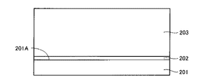
(実施の形態2)
次に、本発明の他の実施の形態である実施の形態2について説明する。実施の形態2における半導体装置であるIGBT200は、炭化珪素基板の面方位およびp型ボディ領域のp型不純物密度に関して上記実施の形態1におけるMOSFET100と同様の構造を有することにより、同様の効果を奏する。
(Embodiment 2)
Next,
すなわち、図7を参照して、本実施の形態における半導体装置であるIGBT200は、導電型がp型である炭化珪素基板201と、バッファ層202(導電型はn型でもp型でもよい)と、炭化珪素からなり導電型がn型のドリフト層203と、導電型がp型の一対のp型ボディ領域204と、導電型がn型のn+領域205と、導電型がp型のp+領域206とを備えている。
That is, referring to FIG. 7,
バッファ層202は、炭化珪素基板201の一方の主面201A上に形成されており、ドリフト層203よりも高濃度の不純物を含んでいる。ドリフト層203は、バッファ層202上に形成され、n型不純物を含むことにより導電型がn型となっている。バッファ層202およびドリフト層203は、炭化珪素基板201の一方の主面201A上に形成されたエピタキシャル成長層である。
一対のp型ボディ領域204は、エピタキシャル成長層において、炭化珪素基板201側の主面とは反対側の主面203Aを含むように互いに分離して形成され、p型不純物を含むことにより、導電型がp型となっている。p型ボディ領域204に含まれるp型不純物は、たとえばアルミニウム(Al)、硼素(B)などである。
The pair of p-
n+領域205は、上記主面203Aを含み、かつp型ボディ領域204に取り囲まれるように、一対のp型ボディ領域204のそれぞれの内部に形成されている。n+領域205は、n型不純物、たとえばPなどをドリフト層203に含まれるn型不純物よりも高い濃度(密度)で含んでいる。p+領域206は、上記主面203Aを含み、かつp型ボディ領域204に取り囲まれるとともに、n+領域205に隣接するように一対のp型ボディ領域204のそれぞれの内部に形成されている。p+領域206は、p型不純物、たとえばAlなどをp型ボディ領域204に含まれるp型不純物よりも高い濃度(密度)で含んでいる。上記バッファ層202、ドリフト層203、p型ボディ領域204、n+領域205およびp+領域206は、活性層207を構成する。
N + region 205 is formed inside each of the pair of p-
さらに、図7を参照して、IGBT200は、ゲート絶縁膜としてのゲート酸化膜291と、ゲート電極293と、一対のエミッタコンタクト電極292と、層間絶縁膜294と、エミッタ配線295と、コレクタ電極296とを備えている。
Further, referring to FIG. 7,
ゲート酸化膜291は、主面203Aに接触し、一方のn+領域205の上部表面から他方のn+領域205の上部表面にまで延在するようにエピタキシャル成長層の主面203A上に形成され、たとえば二酸化珪素(SiO2)からなっている。
ゲート電極293は、一方のn+領域205上から他方のn+領域205上にまで延在するように、ゲート酸化膜291上に接触して配置されている。また、ゲート電極293は、不純物が添加されたポリシリコン、Alなどの導電体からなっている。
エミッタコンタクト電極292は、一対のn+領域205上のそれぞれからp+領域206上にまで達するとともに、主面203Aに接触して配置されている。また、エミッタコンタクト電極292は、たとえばニッケルシリサイドなど、n+領域205およびp+領域206の両方にオーミックコンタクト可能な材料からなっている。
The
層間絶縁膜294は、ドリフト層203の主面203A上においてゲート電極293を取り囲み、かつ一方のp型ボディ領域204上から他方のp型ボディ領域204上にまで延在するように形成され、たとえば絶縁体である二酸化珪素(SiO2)からなっている。
エミッタ配線295は、ドリフト層203の主面203A上において、層間絶縁膜294を取り囲み、かつエミッタコンタクト電極292の上部表面上にまで延在している。また、エミッタ配線295は、Alなどの導電体からなり、エミッタコンタクト電極292を介してn+領域205と電気的に接続されている。
コレクタ電極296は、炭化珪素基板201においてドリフト層203が形成される側とは反対側の主面に接触して形成されている。このコレクタ電極296は、たとえばニッケルシリサイドなど、炭化珪素基板201とオーミックコンタクト可能な材料からなっており、炭化珪素基板201と電気的に接続されている。
次に、IGBT200の動作について説明する。図7を参照して、ゲート電極293に電圧を印加し、当該電圧が閾値を超えると、ゲート電極293下のゲート酸化膜291に接するp型ボディ領域204に反転層が形成され、n+領域205とドリフト層203とが電気的に接続される。これにより、n+領域205からドリフト層203に電子が注入され、これに対応して炭化珪素基板201からバッファ層202を介して正孔がドリフト層203に供給される。その結果、IGBT200がオン状態となり、ドリフト層203に伝導度変調が生じてエミッタコンタクト電極292−コレクタ電極296間の抵抗が低下した状態で電流が流れる。一方、ゲート電極293に印加される上記電圧が閾値以下の場合、上記反転層が形成されないため、ドリフト層203とp型ボディ領域204との間が逆バイアスの状態が維持される。その結果、IGBT200がオフ状態となり、電流は流れない。
Next, the operation of the
ここで、IGBT200においては、炭化珪素基板201の主面201Aの{0001}面に対するオフ角は50°以上65°以下となっている。そのため、p型不純物密度が5×1016cm−3以上という高いドーピング密度のp型ボディ領域204を形成し、閾値電圧をプラス側にシフトさせた場合でも、上記チャネル領域におけるキャリア(電子)の移動度(チャネル移動度)の低下が抑制される。その結果、IGBT200は、チャネル移動度の低下を抑制しつつ閾値電圧を高く設定することが可能なIGBTとなっている。なお、本実施の形態における炭化珪素基板201およびp型ボディ領域204は、それぞれ実施の形態1における炭化珪素基板1およびp型ボディ領域4に対応する。そして、炭化珪素基板1および炭化珪素基板201の面方位、ならびにp型ボディ領域4およびp型ボディ領域204のp型不純物密度については、それぞれ同様の構成を有するものとすることができる。
Here, in
次に、実施の形態2におけるIGBT200の製造方法の一例について、図8〜図11を参照して説明する。図8を参照して、本実施の形態におけるIGBT200の製造方法では、まず工程(S210)として炭化珪素基板準備工程が実施される。この工程(S210)では、図9を参照して、{0001}面に対するオフ角が50°以上65°以下である主面201Aを有する炭化珪素基板201が準備される。
Next, an example of a method for manufacturing the
次に、工程(S220)としてエピタキシャル成長工程が実施される。この工程(S220)では、図9を参照して、エピタキシャル成長により炭化珪素基板201の一方の主面201A上にバッファ層202およびドリフト層203が順次形成される。
Next, an epitaxial growth step is performed as a step (S220). In this step (S220), referring to FIG. 9,
次に、工程(S230)としてイオン注入工程が実施される。この工程(S230)では、図9および図10を参照して、まずp型ボディ領域204を形成するためのイオン注入が実施される。具体的には、たとえばAl(アルミニウム)イオンがドリフト層203に注入されることにより、p型ボディ領域204が形成される。次に、n+領域205を形成するためのイオン注入が実施される。具体的には、たとえばP(リン)イオンがp型ボディ領域204に注入されることにより、p型ボディ領域204内にn+領域205が形成される。さらに、p+領域206を形成するためのイオン注入が実施される。具体的には、たとえばAlイオンがp型ボディ領域204に注入されることにより、p型ボディ領域204内にp+領域206が形成される。上記イオン注入は、たとえばドリフト層203の主面上に二酸化珪素(SiO2)からなり、イオン注入を実施すべき所望の領域に開口を有するマスク層を形成して実施することができる。
Next, an ion implantation step is performed as a step (S230). In this step (S230), referring to FIGS. 9 and 10, first, ion implantation for forming p
次に、工程(S240)として活性化アニール工程が実施される。この工程(S240)は、では、たとえばアルゴンなどの不活性ガス雰囲気中において1700℃に加熱し、30分間保持する熱処理が実施される。これにより、上記工程(S230)において注入された不純物が活性化する。 Next, an activation annealing step is performed as a step (S240). In this step (S240), a heat treatment is performed in which heating is performed at 1700 ° C. in an inert gas atmosphere such as argon and held for 30 minutes. Thereby, the impurities implanted in the step (S230) are activated.
次に、工程(S250)として酸化膜形成工程が実施される。この工程(S250)では、図10および図11を参照して、たとえば酸素雰囲気中において1300℃に加熱して60分間保持する熱処理が実施されることにより、酸化膜(ゲート酸化膜)291が形成される。 Next, an oxide film forming step is performed as a step (S250). In this step (S250), referring to FIGS. 10 and 11, for example, an oxide film (gate oxide film) 291 is formed by performing a heat treatment of heating to 1300 ° C. and holding for 60 minutes in an oxygen atmosphere. Is done.
次に、工程(S260)および(S270)としてNOアニール工程およびArアニール工程が実施される。この工程(S260)および(S270)は、実施の形態1における工程(S160)および(S170)と同様に実施することができる。これにより、最終的に得られるIGBT200のチャネル移動度を向上させることができる。 Next, a NO annealing step and an Ar annealing step are performed as steps (S260) and (S270). Steps (S260) and (S270) can be performed in the same manner as steps (S160) and (S170) in the first embodiment. Thereby, the channel mobility of IGBT200 finally obtained can be improved.
次に、工程(S280)として電極形成工程が実施される。図7を参照して、この工程(S280)では、たとえばCVD法により、不純物が添加されて導電体となっているポリシリコンからなるゲート電極293が形成された後、たとえばCVD法により、絶縁体であるSiO2からなる層間絶縁膜294が、主面203A上においてゲート電極293を取り囲むように形成される。次に、たとえば蒸着法により形成されたニッケル(Ni)膜が加熱されてシリサイド化されることにより、エミッタコンタクト電極292およびコレクタ電極296が形成される。次に、たとえば蒸着法により、導電体であるAlからなるエミッタ配線295が、主面203A上において、層間絶縁膜294を取り囲むとともに、n+領域205およびエミッタコンタクト電極292の上部表面上にまで延在するように形成される。以上の手順により、本実施の形態におけるIGBT200が完成する。
Next, an electrode forming step is performed as a step (S280). Referring to FIG. 7, in this step (S280), after forming
p型ボディ領域におけるp型不純物のドーピング密度と閾値電圧との関係を確認する実験を行なった。具体的には、まず、上記実施の形態1と同様にNOアニール工程およびArアニール工程を含むプロセスにより、実験用のMOSFET(サンプル)を作製した。ここで、p型ボディ領域におけるp型不純物のドーピング密度の異なる複数のサンプルを作製した。そして、各サンプルについて閾値電圧を測定した。 An experiment was conducted to confirm the relationship between the doping density of the p-type impurity and the threshold voltage in the p-type body region. Specifically, first, an experimental MOSFET (sample) was fabricated by a process including a NO annealing step and an Ar annealing step as in the first embodiment. Here, a plurality of samples having different p-type impurity doping densities in the p-type body region were produced. And the threshold voltage was measured about each sample.
実験結果を図12に示す。図12において、横軸はp型ボディ領域におけるp型不純物のドーピング密度、縦軸は閾値電圧を示している。また、図12において、丸印が実験の結果得られたデータ点である。一方、図12における曲線は、上記ドーピング密度と閾値電圧との関係の理論曲線である。理論曲線は、以下の式(1)に対応するものである。なお、式(1)においてniは真性キャリア密度、Coxは酸化膜容量、φmおよびφsは、それぞれ金属および半導体の仕事関数、ΔVQeffは実効固定電荷による電圧シフト成分を示す。また、Qは電気素量を示す(Q=1.6×10⁻¹⁹C)。ここでは、実験結果より、ΔVQeff=−1.9Vとした。 The experimental results are shown in FIG. In FIG. 12, the horizontal axis represents the doping density of the p-type impurity in the p-type body region, and the vertical axis represents the threshold voltage. In FIG. 12, circles are data points obtained as a result of the experiment. On the other hand, the curve in FIG. 12 is a theoretical curve of the relationship between the doping density and the threshold voltage. The theoretical curve corresponds to the following formula (1). Incidentally, n i is the intrinsic carrier density in the formula (1), C ox is the oxide film capacitance, phi m and phi s are each a metal and a semiconductor work function, [Delta] V Qeff shows the voltage shift component due to the effective fixed charge. Further, Q represents an elementary electric quantity (Q = 1.6 × 10 −19 C). Here, from the experimental results, ΔV Qeff = −1.9V.

図12を参照して、実験により得られたデータ点は理論曲線に沿って分布している。そして、図12より、p型ボディ領域におけるp型不純物のドーピング密度を8×1016cm−3以上とすることにより、安定してプラスの閾値電圧が得られる、すなわちノーマリーオフを達成できることが分かる。 Referring to FIG. 12, the data points obtained by the experiment are distributed along the theoretical curve. From FIG. 12, by setting the doping density of the p-type impurity in the p-type body region to 8 × 10 16 cm −3 or more, a positive threshold voltage can be stably obtained, that is, normally-off can be achieved. I understand.
p型ボディ領域におけるp型不純物のドーピング密度とチャネル移動度との関係を調査する実験を行なった。実験の手順は以下の通りである。 An experiment was conducted to investigate the relationship between the doping density of the p-type impurity and the channel mobility in the p-type body region. The experimental procedure is as follows.
まず、一方の主面の面方位が(0−33−8)面である炭化珪素基板を準備し、当該主面上にエピタキシャル成長層等を形成してMOSFETのサンプルを作製した。このとき、p型ボディ領域におけるp型不純物のドーピング密度を2×1016cm−3〜1×1017cm−3の範囲で変化させた複数のサンプルを作製した。なお、ゲート酸化膜の形成は酸素雰囲気中で1200〜1300℃に加熱し、約60分間保持することにより実施した。その後、NO雰囲気中で1100〜1200℃に加熱し、約60分間保持することによりNOアニール処理を実施した。さらにその後、Ar雰囲気中で1200〜1300℃に加熱し、約60分間保持することによりArアニール処理を実施した(実施例)。 First, a silicon carbide substrate in which the plane orientation of one main surface is a (0-33-8) plane was prepared, and an epitaxial growth layer or the like was formed on the main surface to prepare a MOSFET sample. At this time, a plurality of samples in which the doping density of the p-type impurity in the p-type body region was changed in the range of 2 × 10 16 cm −3 to 1 × 10 17 cm −3 was produced. The gate oxide film was formed by heating to 1200 to 1300 ° C. in an oxygen atmosphere and holding it for about 60 minutes. Thereafter, heating to 1100 to 1200 ° C. in a NO atmosphere and holding for about 60 minutes performed a NO annealing treatment. Furthermore, Ar annealing treatment was performed by heating to 1200 to 1300 ° C. in an Ar atmosphere and holding for about 60 minutes (Example).
一方、比較のため、一方の主面の面方位が(0001)面である炭化珪素基板を準備し、同様にMOSFETのサンプルを作製した(比較例)。そして、各サンプルのチャネル移動度を測定した。実験結果を図13および図14に示す。図13および図14において、横軸はp型ボディ領域におけるp型不純物のドーピング密度、縦軸はMOSFETのチャネル移動度を示している。 On the other hand, for comparison, a silicon carbide substrate in which the plane orientation of one main surface is the (0001) plane was prepared, and a MOSFET sample was similarly manufactured (comparative example). And the channel mobility of each sample was measured. Experimental results are shown in FIG. 13 and FIG. 13 and 14, the horizontal axis represents the doping density of the p-type impurity in the p-type body region, and the vertical axis represents the channel mobility of the MOSFET.
図14を参照して、面方位が(0001)面である主面上にエピタキシャル成長層等を形成して得られた比較例のMOSFETにおいては、ドーピング密度が2×1016cm−3から1×1017cm−3に上昇することにより、チャネル移動度が25%程度低下している。これに対し、面方位が(0−33−8)面である主面上にエピタキシャル成長層等を形成して得られた実施例のMOSFETにおいては、ドーピング密度が2×1016cm−3から1×1017cm−3に上昇しても、チャネル移動度はほとんど低下していない。さらに、実施例のMOSFETにおけるチャネル移動度は、比較例のMOSFETにおけるチャネル移動度に比べて絶対値において大幅に高くなっている。つまり、実施例の半導体装置は比較例の半導体装置に比べてチャネル移動度が高く、p型ボディ領域におけるドーピング密度が上昇するとその差はさらに広がることが分かる。以上の実験結果より、本発明の半導体装置によれば、チャネル移動度の低下を抑制しつつ閾値電圧をプラス側にシフト可能であることが確認された。 Referring to FIG. 14, in the MOSFET of the comparative example obtained by forming an epitaxial growth layer or the like on the main surface whose plane orientation is the (0001) plane, the doping density is 2 × 10 16 cm −3 to 1 ×. By increasing to 10 17 cm −3 , the channel mobility is reduced by about 25%. On the other hand, in the MOSFET of the example obtained by forming an epitaxial growth layer or the like on the main surface whose plane orientation is the (0-33-8) plane, the doping density is 2 × 10 16 cm −3 to 1 Even if it rises to x10 17 cm −3 , the channel mobility hardly decreases. Further, the channel mobility in the MOSFET of the example is significantly higher in absolute value than the channel mobility in the MOSFET of the comparative example. That is, it can be seen that the semiconductor device of the example has higher channel mobility than the semiconductor device of the comparative example, and the difference further increases as the doping density in the p-type body region increases. From the above experimental results, it was confirmed that the threshold voltage can be shifted to the positive side while suppressing a decrease in channel mobility according to the semiconductor device of the present invention.
本発明の半導体装置であるMOSFETの閾値電圧について調査する実験を行なった。対象となるMOSFETは、上記実施の形態1に示す製造方法により製造した。このMOSFETを用いて、ゲート電圧を変化させた場合におけるドレイン電流の値を測定した。そして、この測定結果をプロットしたグラフを作成し、当該グラフから閾値電圧を求めた。このとき、同一の測定結果について、ドレイン電流をlogスケールとリニアスケールとの2通りでプロットし、閾値電圧を求めた。作成されたグラフを図15に示す。 An experiment was conducted to investigate the threshold voltage of a MOSFET which is a semiconductor device of the present invention. The target MOSFET was manufactured by the manufacturing method shown in the first embodiment. Using this MOSFET, the value of the drain current when the gate voltage was changed was measured. And the graph which plotted this measurement result was created, and the threshold voltage was calculated | required from the said graph. At this time, with respect to the same measurement result, the drain current was plotted in two ways, a log scale and a linear scale, to obtain a threshold voltage. The created graph is shown in FIG.
図15において横軸はゲート電圧(VG)、左縦軸はlogスケールのドレイン電流(Id)、右縦軸はリニアスケールのドレイン電流(Id)を示している。また、図15において、太線はlogスケールのドレイン電流(log Id)、細線はリニアスケールのドレイン電流(linear Id)を示している。図15を参照して、リニアスケールのドレイン電流を示す曲線の直線部分を延長して得られる閾値電圧(点B参照)に比べて、logスケールのドレイン電流を示す曲線から得られる閾値電圧(点A参照)は小さくなっている。ここで、上記logスケールのドレイン電流を示す曲線から得られる閾値電圧は、ゲート電圧を上昇させていった場合にp型ボディ領域においてゲート酸化膜に接する領域に最初に薄いチャネル領域(弱反転層)が形成される電圧を示している。本願においては、この弱反転層が形成されるゲート電圧を閾値電圧として取り扱う。 In FIG. 15, the horizontal axis represents the gate voltage (V G ), the left vertical axis represents the log-scale drain current (I d ), and the right vertical axis represents the linear-scale drain current (I d ). In FIG. 15, the bold line indicates the log scale drain current (log I d ), and the thin line indicates the linear scale drain current (linear I d ). Referring to FIG. 15, the threshold voltage (dots) obtained from the curve showing the drain current on the log scale, compared to the threshold voltage (see point B) obtained by extending the linear portion of the curve showing the drain current on the linear scale. A) is smaller. Here, the threshold voltage obtained from the curve indicating the log-scale drain current is a thin channel region (weak inversion layer) first in a region in contact with the gate oxide film in the p-type body region when the gate voltage is increased. ) Indicates the voltage at which it is formed. In the present application, the gate voltage at which the weak inversion layer is formed is treated as a threshold voltage.
本発明の半導体装置であるMOSFETを作製し、閾値電圧の温度依存性を調査する実験を行なった。まず、上記実施の形態1の場合と同様にMOSFETを作製した。このとき、エピタキシャル成長層は、炭化珪素基板のカーボン面側の{03−38}面(すなわち(0−33−8)面)上に形成した。また、p型ボディ領域におけるp型不純物(Al)密度が1×1018cm−3(実施例A)および5×1017cm−3(実施例B)の2種類のMOSFETを作製した。一方、比較のため、同様の製造方法においてエピタキシャル成長層を炭化珪素基板のシリコン面側の{0001}面(すなわち(0001)面)上に形成したMOSFETも作製した(比較例A)。p型ボディ領域におけるp型不純物(Al)密度は2×1016cm−3とした。そして、室温(25℃)〜200℃の温度範囲内において上記実施例および比較例のMOSFETの閾値電圧を調査した。調査結果を図16に示す。図16において、丸印は実施例A、四角印は実施例B、三角印は比較例Aの調査結果を示している。 A MOSFET which is a semiconductor device of the present invention was fabricated, and an experiment was conducted to investigate the temperature dependence of the threshold voltage. First, a MOSFET was manufactured in the same manner as in the first embodiment. At this time, the epitaxial growth layer was formed on the {03-38} plane (that is, (0-33-8) plane) on the carbon plane side of the silicon carbide substrate. Also, two types of MOSFETs having p-type impurity (Al) density in the p-type body region of 1 × 10 18 cm −3 (Example A) and 5 × 10 17 cm −3 (Example B) were produced. On the other hand, for comparison, a MOSFET in which an epitaxial growth layer was formed on the {0001} plane (that is, (0001) plane) of the silicon carbide substrate in the same manufacturing method was also manufactured (Comparative Example A). The p-type impurity (Al) density in the p-type body region was 2 × 10 16 cm −3 . And the threshold voltage of MOSFET of the said Example and comparative example was investigated within the temperature range of room temperature (25 degreeC) -200 degreeC. The survey results are shown in FIG. In FIG. 16, the circles indicate the results of Example A, the squares indicate the results of Example B, and the triangles indicate the results of Comparative Example A.
図16を参照して、実施例AおよびBのMOFETの閾値電圧は比較例に比べて高く、室温以上100℃以下の温度範囲において2V以上となっており、安定してノーマリーオフの状態を維持することが可能となっている。特に、実施例AのMOSFETの閾値電圧は100℃において3V以上、かつ200℃において1V以上となっており、より高温においても安定してノーマリーオフの状態を維持することが可能となっている。また、実施例AおよびBにおいては、閾値電圧の温度依存性(図中の近似直線の傾き)がそれぞれ−7mV/℃および−6mV/℃であり−10mV/℃以上となっている。別の観点から説明すると、実施例AおよびBにおいては、温度依存性(図中の近似直線の傾き)の絶対値がそれぞれ7mV/℃および6mV/℃であり、10mV/℃以下となっている。その結果、安定してノーマリーオフの状態を維持することが可能となっている。 Referring to FIG. 16, the threshold voltages of the MOFETs of Examples A and B are higher than those of the comparative example, and are 2 V or higher in a temperature range of room temperature to 100 ° C., and the normally-off state is stable. It is possible to maintain. In particular, the threshold voltage of the MOSFET of Example A is 3 V or higher at 100 ° C. and 1 V or higher at 200 ° C., and it is possible to stably maintain a normally-off state even at higher temperatures. . In Examples A and B, the temperature dependence of the threshold voltage (the slope of the approximate line in the figure) is −7 mV / ° C. and −6 mV / ° C., which is −10 mV / ° C. or higher. From another viewpoint, in Examples A and B, the absolute values of the temperature dependence (slope of the approximate line in the figure) are 7 mV / ° C. and 6 mV / ° C., respectively, and are 10 mV / ° C. or less. . As a result, it is possible to stably maintain a normally-off state.
本発明の半導体装置であるMOSFETを作製し、電子のチャネル移動度の温度依存性を調査する実験を行なった。まず、上記実施の形態1の場合と同様にMOSFETを作製した。このとき、エピタキシャル成長層は、炭化珪素基板のカーボン面側の{03−38}面(すなわち(0−33−8)面)上に形成した(実施例C)。一方、比較のため、同様の製造方法においてエピタキシャル成長層を炭化珪素基板のシリコン面側の{0001}面(すなわち(0001)面)上に形成したMOSFETも作製した(比較例B)。そして、室温(25℃)〜200℃の温度範囲内において上記実施例および比較例のMOSFETの電子のチャネル移動度を調査した。調査結果を図17に示す。図17において、丸印は実施例C、三角印は比較例Bの調査結果を示している。 A MOSFET which is a semiconductor device of the present invention was fabricated, and an experiment was conducted to investigate the temperature dependence of the electron channel mobility. First, a MOSFET was manufactured in the same manner as in the first embodiment. At this time, the epitaxial growth layer was formed on the {03-38} plane (that is, (0-33-8) plane) on the carbon plane side of the silicon carbide substrate (Example C). On the other hand, for comparison, a MOSFET in which an epitaxial growth layer was formed on the {0001} plane (that is, the (0001) plane) of the silicon carbide substrate in the same manufacturing method was also manufactured (Comparative Example B). Then, the channel mobility of electrons in the MOSFETs of the above examples and comparative examples was investigated within a temperature range of room temperature (25 ° C.) to 200 ° C. The survey results are shown in FIG. In FIG. 17, circles indicate the results of Example C, and triangles indicate the results of Comparative Example B.
図17を参照して、実施例CのMOFETのチャネル移動度は比較例Bに比べて高く、室温において30cm2/Vs以上であるだけでなく、100℃において50cm2/Vs以上、150℃において40cm2/Vs以上となっている。また、電子のチャネル移動度の温度依存性も−0.3cm2/Vs℃以上となっている。別の観点から説明すると、電子のチャネル移動度の温度依存性の絶対値が0.3cm2/Vs℃以下となっている。その結果、安定して半導体装置のオン抵抗を抑制することが可能となっている。 Referring to FIG. 17, the channel mobility of the MOFET of Example C is higher than that of Comparative Example B, and is not only 30 cm 2 / Vs or higher at room temperature, but also 50 cm 2 / Vs or higher at 100 ° C. and 150 ° C. It is 40 cm 2 / Vs or more. The temperature dependence of the electron channel mobility is also −0.3 cm 2 / Vs ° C. or higher. From another viewpoint, the absolute value of the temperature dependence of the electron channel mobility is 0.3 cm 2 / Vs ° C. or less. As a result, it is possible to stably suppress the on-resistance of the semiconductor device.
本発明の半導体装置であるMOSFETを作製し、p型ボディ領域におけるp型不純物(Al)密度と閾値電圧との関係を調査する実験を行なった。まず、上記実施の形態1の場合と同様にMOSFETを作製した。このとき、エピタキシャル成長層は、炭化珪素基板のカーボン面側の{03−38}面(すなわち(0−33−8)面)上に形成した。また、p型ボディ領域におけるp型不純物(Al)の密度の異なる5種類のサンプルを作製した。そして、サンプルの電子のチャネル移動度を調査した。調査結果を図18に示す。図18において横軸はp型ボディ領域におけるp型不純物(Al)の密度、縦軸は閾値電圧を示している。 A MOSFET which is a semiconductor device of the present invention was fabricated, and an experiment was conducted to investigate the relationship between the p-type impurity (Al) density and the threshold voltage in the p-type body region. First, a MOSFET was manufactured in the same manner as in the first embodiment. At this time, the epitaxial growth layer was formed on the {03-38} plane (that is, (0-33-8) plane) on the carbon plane side of the silicon carbide substrate. Five types of samples having different p-type impurity (Al) densities in the p-type body region were produced. Then, the electron channel mobility of the sample was investigated. The survey results are shown in FIG. In FIG. 18, the horizontal axis indicates the density of p-type impurity (Al) in the p-type body region, and the vertical axis indicates the threshold voltage.
図18を参照して、p型ボディ領域における不純物密度が上昇するに伴って、閾値電圧が上昇している。そして、不純物密度が8×1016cm−3以上3×1018cm−3以下である領域において閾値電圧が0〜5V程度となっている。また、上述のように、本発明の半導体装置においては、チャネル移動度の低下を抑制しつつp型ボディ領域におけるp型不純物密度を上昇させることが可能であるため、不純物密度が8×1016cm−3〜3×1018cm−3程度であっても十分なチャネル移動度を確保することができる。したがって、本発明の半導体装置においては、p型ボディ領域におけるp型不純物密度を8×1016cm−3以上3×1018cm−3以下とすることにより、珪素を材料として採用した半導体装置と置き換えて使用することが容易であるとともに、安定してノーマリーオフ型である状態を維持することができる。また、不純物密度が高くなることによる大幅なチャネル移動度の低下を回避することができる。
Referring to FIG. 18, the threshold voltage increases as the impurity density in the p-type body region increases. The threshold voltage is about 0 to 5 V in a region where the impurity density is 8 × 10 16 cm −3 or more and 3 × 10 18 cm −3 or less. Further, as described above, in the semiconductor device of the present invention, it is possible to increase the p-type impurity density in the p-type body region while suppressing a decrease in channel mobility, so that the impurity density is 8 × 10 16. Even if it is about
今回開示された実施の形態および実施例はすべての点で例示であって、制限的なものではないと考えられるべきである。本発明の範囲は上記した説明ではなくて特許請求の範囲によって示され、特許請求の範囲と均等の意味、および範囲内でのすべての変更が含まれることが意図される。 The embodiments and examples disclosed herein are illustrative in all respects and should not be construed as being restrictive. The scope of the present invention is defined by the terms of the claims, rather than the description above, and is intended to include any modifications within the scope and meaning equivalent to the terms of the claims.
本発明の半導体装置は、閾値電圧の設定の自由度を高めることが求められる半導体装置に、特に有利に適用され得る。 The semiconductor device of the present invention can be applied particularly advantageously to a semiconductor device that is required to increase the degree of freedom in setting a threshold voltage.
1,201 炭化珪素基板、1A,201A 主面、2,202 バッファ層、3,203 ドリフト層、3A,203A 主面、4,204 p型ボディ領域、5,205 n+領域、6,206 p+領域、7,207 活性層、91,291 ゲート酸化膜(酸化膜)、92 ソースコンタクト電極、93 ゲート電極、94,294 層間絶縁膜、95 ソース配線、96 ドレイン電極、100 MOSFET、200 IGBT、292 エミッタコンタクト電極、293 ゲート電極、295 エミッタ配線、296 コレクタ電極。 1,201 Silicon carbide substrate, 1A, 201A main surface, 2,202 buffer layer, 3,203 drift layer, 3A, 203A main surface, 4,204 p-type body region, 5,205 n + region, 6,206 p + Region, 7,207 active layer, 91,291 gate oxide film (oxide film), 92 source contact electrode, 93 gate electrode, 94,294 interlayer insulating film, 95 source wiring, 96 drain electrode, 100 MOSFET, 200 IGBT, 292 emitter contact electrode, 293 gate electrode, 295 emitter wiring, 296 collector electrode.
Claims (22)
前記主面上に形成され、導電型が第1導電型であるエピタキシャル成長層と、
前記エピタキシャル成長層上に接触して形成された絶縁膜と、
前記エピタキシャル成長層において前記絶縁膜と接触する領域を含むように形成され、導電型が前記第1導電型とは異なる第2導電型であるボディ領域とを備え、
前記ボディ領域における不純物密度は5×1017cm−3以上であり、
前記ボディ領域の、前記絶縁膜と接触する領域にチャネル領域が形成され、前記エピタキシャル成長層と前記絶縁膜との界面におけるバリアハイトは2.2eV以上2.6eV以下である、半導体装置。 A silicon carbide substrate having a main surface with an off angle of 50 ° or more and 65 ° or less with respect to the {0001} plane;
An epitaxial growth layer formed on the main surface and having a conductivity type of the first conductivity type;
An insulating film formed in contact with the epitaxial growth layer;
A body region that is formed to include a region in contact with the insulating film in the epitaxial growth layer and has a second conductivity type different from the first conductivity type;
The impurity density in the body region is 5 × 10 17 cm −3 or more,
A semiconductor device, wherein a channel region is formed in a region of the body region in contact with the insulating film, and a barrier height at an interface between the epitaxial growth layer and the insulating film is 2.2 eV or more and 2.6 eV or less .
前記ゲート電極は前記第2導電型のポリシリコンからなっている、請求項7に記載の半導体装置。 A gate electrode disposed on and in contact with the insulating film;
The semiconductor device according to claim 7, wherein the gate electrode is made of the second conductivity type polysilicon.
前記ゲート電極はn型ポリシリコンからなっている、請求項1から請求項7のいずれか1項に記載の半導体装置。 A gate electrode disposed on and in contact with the insulating film;
The semiconductor device according to claim 1, wherein the gate electrode is made of n-type polysilicon.
Priority Applications (8)
| Application Number | Priority Date | Filing Date | Title |
|---|---|---|---|
| JP2011012510A JP5699628B2 (en) | 2010-07-26 | 2011-01-25 | Semiconductor device |
| KR1020127019037A KR20130092377A (en) | 2010-07-26 | 2011-06-29 | Semiconductor device |
| CN2011800204785A CN103168361A (en) | 2010-07-26 | 2011-06-29 | Semiconductor device |
| CA2796857A CA2796857A1 (en) | 2010-07-26 | 2011-06-29 | Semiconductor device |
| EP11812210.0A EP2600402A4 (en) | 2010-07-26 | 2011-06-29 | Semiconductor device |
| PCT/JP2011/064897 WO2012014617A1 (en) | 2010-07-26 | 2011-06-29 | Semiconductor device |
| TW100126054A TW201210025A (en) | 2010-07-26 | 2011-07-22 | Semiconductor device |
| US13/190,001 US20120018743A1 (en) | 2010-07-26 | 2011-07-25 | Semiconductor device |
Applications Claiming Priority (3)
| Application Number | Priority Date | Filing Date | Title |
|---|---|---|---|
| JP2010167004 | 2010-07-26 | ||
| JP2010167004 | 2010-07-26 | ||
| JP2011012510A JP5699628B2 (en) | 2010-07-26 | 2011-01-25 | Semiconductor device |
Publications (3)
| Publication Number | Publication Date |
|---|---|
| JP2012049491A JP2012049491A (en) | 2012-03-08 |
| JP2012049491A5 JP2012049491A5 (en) | 2014-01-23 |
| JP5699628B2 true JP5699628B2 (en) | 2015-04-15 |
Family
ID=45492856
Family Applications (1)
| Application Number | Title | Priority Date | Filing Date |
|---|---|---|---|
| JP2011012510A Active JP5699628B2 (en) | 2010-07-26 | 2011-01-25 | Semiconductor device |
Country Status (8)
| Country | Link |
|---|---|
| US (1) | US20120018743A1 (en) |
| EP (1) | EP2600402A4 (en) |
| JP (1) | JP5699628B2 (en) |
| KR (1) | KR20130092377A (en) |
| CN (1) | CN103168361A (en) |
| CA (1) | CA2796857A1 (en) |
| TW (1) | TW201210025A (en) |
| WO (1) | WO2012014617A1 (en) |
Families Citing this family (18)
| Publication number | Priority date | Publication date | Assignee | Title |
|---|---|---|---|---|
| US8674439B2 (en) | 2010-08-02 | 2014-03-18 | Microsemi Corporation | Low loss SiC MOSFET |
| JP5668576B2 (en) * | 2011-04-01 | 2015-02-12 | 住友電気工業株式会社 | Silicon carbide semiconductor device |
| JP5751113B2 (en) * | 2011-09-28 | 2015-07-22 | 住友電気工業株式会社 | Method for manufacturing silicon carbide semiconductor device |
| JP5811829B2 (en) * | 2011-12-22 | 2015-11-11 | 住友電気工業株式会社 | Manufacturing method of semiconductor device |
| CN102664192B (en) | 2012-05-08 | 2015-03-11 | 北京大学 | Self-adaptive composite mechanism tunneling field effect transistor (TFET) and preparation method thereof |
| JP2014007310A (en) * | 2012-06-26 | 2014-01-16 | Sumitomo Electric Ind Ltd | Silicon carbide semiconductor device manufacturing method and silicon carbide semiconductor device |
| JP6068042B2 (en) * | 2012-08-07 | 2017-01-25 | 住友電気工業株式会社 | Silicon carbide semiconductor device and manufacturing method thereof |
| JP2014038896A (en) * | 2012-08-13 | 2014-02-27 | Sumitomo Electric Ind Ltd | Silicon carbide semiconductor device |
| JP5646569B2 (en) | 2012-09-26 | 2014-12-24 | 株式会社東芝 | Semiconductor device |
| US9515145B2 (en) * | 2013-02-28 | 2016-12-06 | Mitsubishi Electric Corporation | Vertical MOSFET device with steady on-resistance |
| EP2976786A1 (en) * | 2013-03-21 | 2016-01-27 | Microsemi Corporation | Sic power vertical dmos with increased safe operating area |
| JP6242633B2 (en) * | 2013-09-03 | 2017-12-06 | 株式会社東芝 | Semiconductor device |
| JP6113298B2 (en) * | 2013-11-13 | 2017-04-12 | 三菱電機株式会社 | Manufacturing method of semiconductor device and semiconductor device |
| JP6089015B2 (en) * | 2014-10-17 | 2017-03-01 | 株式会社東芝 | Semiconductor device |
| CN107331603B (en) * | 2017-03-20 | 2020-05-01 | 中国电子科技集团公司第五十五研究所 | Manufacturing method of silicon carbide MOSFET single cell structure |
| CN108257872A (en) * | 2018-01-12 | 2018-07-06 | 北京品捷电子科技有限公司 | The preparation method of SiC bases DI-MOSFET a kind of and SiC bases DI-MOSFET |
| GB2589543A (en) * | 2019-09-09 | 2021-06-09 | Mqsemi Ag | Method for forming a low injection P-type contact region and power semiconductor devices with the same |
| CN111129155A (en) * | 2019-12-25 | 2020-05-08 | 重庆伟特森电子科技有限公司 | Preparation method of low-gate-drain capacitance silicon carbide DI-MOSFET |
Family Cites Families (17)
| Publication number | Priority date | Publication date | Assignee | Title |
|---|---|---|---|---|
| US5877515A (en) * | 1995-10-10 | 1999-03-02 | International Rectifier Corporation | SiC semiconductor device |
| JP2000106428A (en) * | 1998-09-28 | 2000-04-11 | Toshiba Corp | Semiconductor device |
| DE60033829T2 (en) * | 1999-09-07 | 2007-10-11 | Sixon Inc. | SiC SEMICONDUCTOR SHEET, SiC SEMICONDUCTOR ELEMENT AND MANUFACTURING METHOD FOR A SiC SEMICONDUCTOR DISC |
| JP4843854B2 (en) * | 2001-03-05 | 2011-12-21 | 住友電気工業株式会社 | MOS device |
| JP3697211B2 (en) * | 2002-01-10 | 2005-09-21 | 日本原子力研究所 | Silicon carbide semiconductor element and method for forming insulating film thereof |
| US7221010B2 (en) * | 2002-12-20 | 2007-05-22 | Cree, Inc. | Vertical JFET limited silicon carbide power metal-oxide semiconductor field effect transistors |
| JP5368140B2 (en) * | 2003-03-28 | 2013-12-18 | 三菱電機株式会社 | Manufacturing method of vertical MOSFET using SiC |
| JP2005167035A (en) * | 2003-12-03 | 2005-06-23 | Kansai Electric Power Co Inc:The | Silicon carbide semiconductor device and manufacturing method thereof |
| JP4775102B2 (en) * | 2005-05-09 | 2011-09-21 | 住友電気工業株式会社 | Manufacturing method of semiconductor device |
| US7727904B2 (en) * | 2005-09-16 | 2010-06-01 | Cree, Inc. | Methods of forming SiC MOSFETs with high inversion layer mobility |
| EP1981076B1 (en) * | 2006-01-30 | 2012-05-23 | Sumitomo Electric Industries, Ltd. | Method for manufacturing silicon carbide semiconductor device |
| US20090134476A1 (en) * | 2007-11-13 | 2009-05-28 | Thunderbird Technologies, Inc. | Low temperature coefficient field effect transistors and design and fabrication methods |
| JP5504597B2 (en) * | 2007-12-11 | 2014-05-28 | 住友電気工業株式会社 | Silicon carbide semiconductor device and manufacturing method thereof |
| JP2009272365A (en) * | 2008-05-01 | 2009-11-19 | Renesas Technology Corp | Method of manufacturing semiconductor device |
| JP5564781B2 (en) * | 2008-07-07 | 2014-08-06 | 住友電気工業株式会社 | Silicon carbide semiconductor device and manufacturing method thereof |
| TW201044586A (en) * | 2009-03-27 | 2010-12-16 | Sumitomo Electric Industries | Mosfet and method for manufacturing mosfet |
| KR102293198B1 (en) * | 2009-09-16 | 2021-08-24 | 가부시키가이샤 한도오따이 에네루기 켄큐쇼 | Semiconductor device and method for manufacturing the same |
-
2011
- 2011-01-25 JP JP2011012510A patent/JP5699628B2/en active Active
- 2011-06-29 WO PCT/JP2011/064897 patent/WO2012014617A1/en active Application Filing
- 2011-06-29 EP EP11812210.0A patent/EP2600402A4/en not_active Withdrawn
- 2011-06-29 CA CA2796857A patent/CA2796857A1/en not_active Abandoned
- 2011-06-29 KR KR1020127019037A patent/KR20130092377A/en not_active Application Discontinuation
- 2011-06-29 CN CN2011800204785A patent/CN103168361A/en active Pending
- 2011-07-22 TW TW100126054A patent/TW201210025A/en unknown
- 2011-07-25 US US13/190,001 patent/US20120018743A1/en not_active Abandoned
Also Published As
| Publication number | Publication date |
|---|---|
| WO2012014617A1 (en) | 2012-02-02 |
| KR20130092377A (en) | 2013-08-20 |
| CN103168361A (en) | 2013-06-19 |
| US20120018743A1 (en) | 2012-01-26 |
| EP2600402A1 (en) | 2013-06-05 |
| TW201210025A (en) | 2012-03-01 |
| EP2600402A4 (en) | 2013-12-25 |
| JP2012049491A (en) | 2012-03-08 |
| CA2796857A1 (en) | 2012-02-02 |
Similar Documents
| Publication | Publication Date | Title |
|---|---|---|
| JP5699628B2 (en) | Semiconductor device | |
| JP5668576B2 (en) | Silicon carbide semiconductor device | |
| US8610131B2 (en) | Silicon carbide insulated-gate bipolar transistor | |
| EP2725622B1 (en) | Silicon carbide semiconductor element and method for producing same | |
| WO2012169224A1 (en) | Semiconductor device | |
| US8564017B2 (en) | Silicon carbide semiconductor device and method for manufacturing same | |
| WO2010038547A1 (en) | Silicon carbide semiconductor device | |
| KR20110137279A (en) | Insulated gate bipolar transistor | |
| KR20140001947A (en) | Semicondcutor device | |
| JP2015032614A (en) | Silicon carbide semiconductor device and manufacturing method of the same | |
| JP5870672B2 (en) | Semiconductor device | |
| JP5655570B2 (en) | Manufacturing method of semiconductor device | |
| CN104854704A (en) | Silicon carbide semiconductor device | |
| JP5673113B2 (en) | Semiconductor device |
Legal Events
| Date | Code | Title | Description |
|---|---|---|---|
| A621 | Written request for application examination |
Free format text: JAPANESE INTERMEDIATE CODE: A621 Effective date: 20130828 |
|
| A521 | Request for written amendment filed |
Free format text: JAPANESE INTERMEDIATE CODE: A523 Effective date: 20131204 |
|
| A131 | Notification of reasons for refusal |
Free format text: JAPANESE INTERMEDIATE CODE: A131 Effective date: 20140527 |
|
| A521 | Request for written amendment filed |
Free format text: JAPANESE INTERMEDIATE CODE: A523 Effective date: 20140702 |
|
| TRDD | Decision of grant or rejection written | ||
| A01 | Written decision to grant a patent or to grant a registration (utility model) |
Free format text: JAPANESE INTERMEDIATE CODE: A01 Effective date: 20150120 |
|
| A61 | First payment of annual fees (during grant procedure) |
Free format text: JAPANESE INTERMEDIATE CODE: A61 Effective date: 20150202 |
|
| R150 | Certificate of patent or registration of utility model |
Ref document number: 5699628 Country of ref document: JP Free format text: JAPANESE INTERMEDIATE CODE: R150 |
|
| R250 | Receipt of annual fees |
Free format text: JAPANESE INTERMEDIATE CODE: R250 |
|
| R250 | Receipt of annual fees |
Free format text: JAPANESE INTERMEDIATE CODE: R250 |
|
| R250 | Receipt of annual fees |
Free format text: JAPANESE INTERMEDIATE CODE: R250 |
|
| R250 | Receipt of annual fees |
Free format text: JAPANESE INTERMEDIATE CODE: R250 |
|
| R250 | Receipt of annual fees |
Free format text: JAPANESE INTERMEDIATE CODE: R250 |
|
| R250 | Receipt of annual fees |
Free format text: JAPANESE INTERMEDIATE CODE: R250 |
|
| R250 | Receipt of annual fees |
Free format text: JAPANESE INTERMEDIATE CODE: R250 |