JP5564781B2 - Silicon carbide semiconductor device and manufacturing method thereof - Google Patents
Silicon carbide semiconductor device and manufacturing method thereof Download PDFInfo
- Publication number
- JP5564781B2 JP5564781B2 JP2008292370A JP2008292370A JP5564781B2 JP 5564781 B2 JP5564781 B2 JP 5564781B2 JP 2008292370 A JP2008292370 A JP 2008292370A JP 2008292370 A JP2008292370 A JP 2008292370A JP 5564781 B2 JP5564781 B2 JP 5564781B2
- Authority
- JP
- Japan
- Prior art keywords
- semiconductor layer
- silicon carbide
- insulating film
- conductivity type
- type impurity
- Prior art date
- Legal status (The legal status is an assumption and is not a legal conclusion. Google has not performed a legal analysis and makes no representation as to the accuracy of the status listed.)
- Active
Links
- 239000004065 semiconductor Substances 0.000 title claims description 356
- 229910010271 silicon carbide Inorganic materials 0.000 title claims description 149
- HBMJWWWQQXIZIP-UHFFFAOYSA-N silicon carbide Chemical compound [Si+]#[C-] HBMJWWWQQXIZIP-UHFFFAOYSA-N 0.000 title claims description 142
- 238000004519 manufacturing process Methods 0.000 title claims description 47
- 239000012535 impurity Substances 0.000 claims description 172
- IJGRMHOSHXDMSA-UHFFFAOYSA-N Atomic nitrogen Chemical compound N#N IJGRMHOSHXDMSA-UHFFFAOYSA-N 0.000 claims description 106
- 238000009792 diffusion process Methods 0.000 claims description 106
- 239000000758 substrate Substances 0.000 claims description 60
- 229910052757 nitrogen Inorganic materials 0.000 claims description 53
- 239000013078 crystal Substances 0.000 claims description 48
- 238000000034 method Methods 0.000 claims description 26
- 238000010438 heat treatment Methods 0.000 claims description 23
- 239000007789 gas Substances 0.000 claims description 22
- 239000011261 inert gas Substances 0.000 claims description 14
- 230000007547 defect Effects 0.000 claims description 9
- XUIMIQQOPSSXEZ-UHFFFAOYSA-N Silicon Chemical compound [Si] XUIMIQQOPSSXEZ-UHFFFAOYSA-N 0.000 claims 1
- 238000003763 carbonization Methods 0.000 claims 1
- 229910052710 silicon Inorganic materials 0.000 claims 1
- 239000010703 silicon Substances 0.000 claims 1
- 238000005530 etching Methods 0.000 description 32
- 230000015572 biosynthetic process Effects 0.000 description 31
- XKRFYHLGVUSROY-UHFFFAOYSA-N Argon Chemical compound [Ar] XKRFYHLGVUSROY-UHFFFAOYSA-N 0.000 description 28
- 238000000137 annealing Methods 0.000 description 28
- 230000003647 oxidation Effects 0.000 description 20
- 238000007254 oxidation reaction Methods 0.000 description 20
- MWUXSHHQAYIFBG-UHFFFAOYSA-N Nitric oxide Chemical compound O=[N] MWUXSHHQAYIFBG-UHFFFAOYSA-N 0.000 description 16
- 229910052786 argon Inorganic materials 0.000 description 14
- 230000000052 comparative effect Effects 0.000 description 14
- 238000000206 photolithography Methods 0.000 description 14
- 238000005468 ion implantation Methods 0.000 description 13
- PXHVJJICTQNCMI-UHFFFAOYSA-N Nickel Chemical compound [Ni] PXHVJJICTQNCMI-UHFFFAOYSA-N 0.000 description 12
- 239000000969 carrier Substances 0.000 description 8
- 230000004913 activation Effects 0.000 description 6
- 238000005275 alloying Methods 0.000 description 6
- 229910052751 metal Inorganic materials 0.000 description 6
- 239000002184 metal Substances 0.000 description 6
- 229910052759 nickel Inorganic materials 0.000 description 6
- 238000000059 patterning Methods 0.000 description 6
- 230000002265 prevention Effects 0.000 description 6
- 229910052782 aluminium Inorganic materials 0.000 description 5
- XAGFODPZIPBFFR-UHFFFAOYSA-N aluminium Chemical compound [Al] XAGFODPZIPBFFR-UHFFFAOYSA-N 0.000 description 5
- 150000002500 ions Chemical class 0.000 description 5
- 238000004544 sputter deposition Methods 0.000 description 5
- ZOXJGFHDIHLPTG-UHFFFAOYSA-N Boron Chemical compound [B] ZOXJGFHDIHLPTG-UHFFFAOYSA-N 0.000 description 4
- OAICVXFJPJFONN-UHFFFAOYSA-N Phosphorus Chemical compound [P] OAICVXFJPJFONN-UHFFFAOYSA-N 0.000 description 4
- 229910052796 boron Inorganic materials 0.000 description 4
- 238000005229 chemical vapour deposition Methods 0.000 description 4
- 230000007423 decrease Effects 0.000 description 4
- 238000009826 distribution Methods 0.000 description 4
- 238000011156 evaluation Methods 0.000 description 4
- 239000011574 phosphorus Substances 0.000 description 4
- 229910052698 phosphorus Inorganic materials 0.000 description 4
- 238000001004 secondary ion mass spectrometry Methods 0.000 description 4
- 230000005669 field effect Effects 0.000 description 3
- -1 for example Substances 0.000 description 2
- 238000009413 insulation Methods 0.000 description 2
- 229910044991 metal oxide Inorganic materials 0.000 description 2
- 150000004706 metal oxides Chemical class 0.000 description 2
- QVGXLLKOCUKJST-UHFFFAOYSA-N atomic oxygen Chemical compound [O] QVGXLLKOCUKJST-UHFFFAOYSA-N 0.000 description 1
- 230000001747 exhibiting effect Effects 0.000 description 1
- 238000012986 modification Methods 0.000 description 1
- 230000004048 modification Effects 0.000 description 1
- QJGQUHMNIGDVPM-UHFFFAOYSA-N nitrogen group Chemical group [N] QJGQUHMNIGDVPM-UHFFFAOYSA-N 0.000 description 1
- 239000001301 oxygen Substances 0.000 description 1
- 229910052760 oxygen Inorganic materials 0.000 description 1
Images


Landscapes
- Formation Of Insulating Films (AREA)
Description
本発明は、炭化ケイ素半導体装置およびその製造方法に関し、特に、優れた電気的特性を示す炭化ケイ素半導体装置およびその製造方法に関する。 The present invention relates to a silicon carbide semiconductor device and a manufacturing method thereof, and more particularly, to a silicon carbide semiconductor device exhibiting excellent electrical characteristics and a manufacturing method thereof.
従来から、炭化ケイ素(SiC)を用いた炭化ケイ素半導体装置が知られており、その一例が、たとえば、国際公開第01/018872号パンフレット(以下、「特許文献1」という。)に記載されている。特許文献1には、面方位がほぼ{03−38}であり4H型ポリタイプのSiC基板を用いて形成された炭化ケイ素半導体装置としてのMOS型電界効果トランジスタ(MOSFET)が記載されている。特許文献1に記載されたMOSFETにおいては、ゲート酸化膜をドライ酸化により形成しており、高いチャネル移動度(約100cm2/Vs)を実現できるとされている。
SiCを用いた炭化ケイ素半導体装置の優れた電気的特性を安定して発揮させるためには、高いチャネル移動度を再現性良く実現することが求められる。 In order to stably exhibit the excellent electrical characteristics of the silicon carbide semiconductor device using SiC, it is required to realize high channel mobility with good reproducibility.
しかしながら、本発明者らが検討した結果、特許文献1に記載されたMOSFETにおいてもチャネル移動度が十分に高くならない場合があることを見い出した。 However, as a result of studies by the present inventors, it has been found that the channel mobility may not be sufficiently high even in the MOSFET described in Patent Document 1.
上記の事情に鑑みて、本発明の目的は、高いチャネル移動度を再現性良く実現することができる炭化ケイ素半導体装置およびその製造方法を提供することにある。 In view of the above circumstances, an object of the present invention is to provide a silicon carbide semiconductor device capable of realizing high channel mobility with high reproducibility and a method for manufacturing the same.
本発明は、{0001}面に対して50°以上65°以下の範囲内で傾いている表面を有する炭化ケイ素からなる半導体層と、半導体層の表面に接触するように形成された絶縁膜とを備え、半導体層の表面と絶縁膜との界面から10nm以内の領域における窒素濃度の最大値が1×1021cm-3以上であって、半導体層の表面内において<−2110>方向に直交する方向±10°の範囲内にチャネル長方向を有する炭化ケイ素半導体装置である。 The present invention relates to a semiconductor layer made of silicon carbide having a surface inclined within a range of 50 ° to 65 ° with respect to the {0001} plane, and an insulating film formed so as to be in contact with the surface of the semiconductor layer. The maximum value of the nitrogen concentration in the region within 10 nm from the interface between the surface of the semiconductor layer and the insulating film is 1 × 10 21 cm −3 or more, and is orthogonal to the <−2110> direction in the surface of the semiconductor layer This is a silicon carbide semiconductor device having a channel length direction within a range of ± 10 °.
また、本発明は、第1導電型の炭化ケイ素からなる基板と、基板の表面上に形成され、基板よりも低濃度の第1導電型不純物を含み、{0001}面に対して50°以上65°以下の範囲内で傾いている表面を有する第1導電型の炭化ケイ素からなる半導体層と、半導体層の表面内に形成された第2導電型不純物拡散層と、第2導電型不純物拡散層の表面内に形成された第1導電型不純物拡散層と、半導体層の表面に接触するように形成された絶縁膜と、半導体層の表面の絶縁膜の形成部分以外の領域の少なくとも一部に接触するように形成されたソース電極と、絶縁膜上に形成されたゲート電極と、基板の半導体層の形成側と反対側の表面に形成されたドレイン電極とを備え、半導体層の表面と絶縁膜との界面から10nm以内の領域における窒素濃度の最大値が1×1021cm-3以上であり、半導体層の表面内において<−2110>方向に直交する方向±10°の範囲内にチャネル長方向を有する炭化ケイ素半導体装置である。 The present invention also includes a substrate made of silicon carbide of the first conductivity type, a first conductivity type impurity formed on the surface of the substrate and having a lower concentration than the substrate, and at least 50 ° with respect to the {0001} plane. A semiconductor layer made of silicon carbide of the first conductivity type having a surface inclined within a range of 65 ° or less, a second conductivity type impurity diffusion layer formed in the surface of the semiconductor layer, and a second conductivity type impurity diffusion A first conductivity type impurity diffusion layer formed in the surface of the layer; an insulating film formed so as to be in contact with the surface of the semiconductor layer; and at least a part of a region other than a portion where the insulating film is formed on the surface of the semiconductor layer A source electrode formed so as to be in contact with the gate electrode, a gate electrode formed on the insulating film, and a drain electrode formed on a surface of the substrate opposite to the side on which the semiconductor layer is formed , In a region within 10 nm from the interface with the insulating film The maximum value of the oxygen concentration is not more than 1 × 10 21 cm -3, is silicon carbide semiconductor device having a channel length direction in a range of directions ± 10 ° orthogonal to the <-2110> direction in the surface of the semiconductor layer .
また、本発明は、第1導電型の炭化ケイ素からなる基板と、基板上に形成され、基板よりも低濃度の第1導電型不純物を含み、{0001}面に対して50°以上65°以下の範囲内で傾いている表面を有する第1導電型の炭化ケイ素からなる半導体層と、半導体層の表面内に形成された第2導電型不純物拡散層と、第2導電型不純物拡散層の表面内に形成された第1導電型不純物拡散層と、半導体層の表面に接触するように形成された絶縁膜と、半導体層の表面の絶縁膜の形成部分以外の領域の一部に接触するように形成されたソース電極と、半導体層の表面の絶縁膜の形成部分以外の領域の他の一部に接触するように形成されたドレイン電極と、絶縁膜上に形成されたゲート電極とを備え、半導体層の表面と絶縁膜との界面から10nm以内の領域における窒素濃度の最大値が1×1021cm-3以上であり、半導体層の前記表面内において<−2110>方向に直交する方向±10°の範囲内にチャネル長方向を有する炭化ケイ素半導体装置である。 Further, the present invention includes a substrate made of silicon carbide of the first conductivity type, and a first conductivity type impurity formed on the substrate and having a lower concentration than the substrate, and is 50 ° to 65 ° with respect to the {0001} plane. A semiconductor layer made of silicon carbide of the first conductivity type having a surface inclined within the following range, a second conductivity type impurity diffusion layer formed in the surface of the semiconductor layer, and a second conductivity type impurity diffusion layer. The first conductivity type impurity diffusion layer formed in the surface, the insulating film formed so as to be in contact with the surface of the semiconductor layer, and a part of the region other than the insulating film forming portion on the surface of the semiconductor layer A source electrode formed in such a manner, a drain electrode formed so as to be in contact with another part of the region other than the insulating film forming portion on the surface of the semiconductor layer, and a gate electrode formed on the insulating film. includes, within 10nm from the interface between the surface and the insulating film of the semiconductor layer And the maximum value of the nitrogen concentration is less than 1 × 10 21 cm -3 in the region, the silicon carbide semiconductor having a channel length direction in a range of directions ± 10 ° orthogonal to the <-2110> direction in the inner surface of the semiconductor layer Device.
ここで、本発明の炭化ケイ素半導体装置においては、ソース電極の表面がストライプ状であることが好ましい。 Here, in the silicon carbide semiconductor device of the present invention, the surface of the source electrode is preferably striped.
また、本発明の炭化ケイ素半導体装置においては、ソース電極の表面がハニカム状であることが好ましい。 In the silicon carbide semiconductor device of the present invention, it is preferable that the surface of the source electrode has a honeycomb shape.
また、本発明の炭化ケイ素半導体装置において、半導体層の表面は{03−38}面に対して±5°の範囲内で傾いている結晶面であることが好ましい。 In the silicon carbide semiconductor device of the present invention, the surface of the semiconductor layer is preferably a crystal plane inclined within a range of ± 5 ° with respect to the {03-38} plane.
さらに、本発明は、{0001}面に対して50°以上65°以下の範囲内で傾いている表面を有する炭化ケイ素からなる半導体層を形成する工程と、半導体層の表面内において<−2110>方向に直交する方向を調査する工程と、半導体層の表面内において<−2110>方向に直交する方向±10°の範囲内にチャネル長方向が形成されるように半導体層の表面の一部に接触する絶縁膜を形成する工程と、半導体層の表面と絶縁膜との界面から10nm以内の領域における窒素濃度の最大値が1×1021cm-3以上となるように窒素濃度を調整する工程とを含む炭化ケイ素半導体装置の製造方法である。 Furthermore, the present invention includes a step of forming a semiconductor layer made of silicon carbide having a surface inclined within a range of 50 ° to 65 ° with respect to the {0001} plane, and <−2110 within the surface of the semiconductor layer. The step of investigating the direction orthogonal to the direction, and a part of the surface of the semiconductor layer so that the channel length direction is formed within the range of ± 10 ° in the direction orthogonal to the <−2110> direction in the surface of the semiconductor layer And adjusting the nitrogen concentration so that the maximum value of the nitrogen concentration in a region within 10 nm from the interface between the surface of the semiconductor layer and the insulating film is 1 × 10 21 cm −3 or more. A method of manufacturing a silicon carbide semiconductor device including a process.
ここで、本発明の炭化ケイ素半導体装置の製造方法においては、半導体層に含まれる欠陥の方位に基づいて半導体層の表面内において<−2110>方向に直交する方向を調査することが好ましい。 Here, in the method for manufacturing a silicon carbide semiconductor device of the present invention, it is preferable to investigate the direction orthogonal to the <−2110> direction in the surface of the semiconductor layer based on the orientation of the defects contained in the semiconductor layer.
また、本発明の炭化ケイ素半導体装置の製造方法において、窒素濃度を調整する工程は、絶縁膜が形成された半導体層を、窒素を含有するガスの雰囲気中で熱処理する工程を含むことが好ましい。 In the method for manufacturing a silicon carbide semiconductor device of the present invention, the step of adjusting the nitrogen concentration preferably includes a step of heat-treating the semiconductor layer on which the insulating film is formed in an atmosphere of a nitrogen-containing gas.
また、本発明の炭化ケイ素半導体装置の製造方法において、窒素濃度を調整する工程は、熱処理後の半導体層を不活性ガスの雰囲気中で熱処理する工程を含むことが好ましい。 In the method for manufacturing a silicon carbide semiconductor device of the present invention, the step of adjusting the nitrogen concentration preferably includes a step of heat-treating the semiconductor layer after the heat treatment in an inert gas atmosphere.
本発明によれば、高いチャネル移動度を再現性良く実現することができる炭化ケイ素半導体装置およびその製造方法を提供することができる。 ADVANTAGE OF THE INVENTION According to this invention, the silicon carbide semiconductor device which can implement | achieve high channel mobility with sufficient reproducibility, and its manufacturing method can be provided.
以下、本発明の実施の形態について説明する。なお、本発明の図面において、同一の参照符号は、同一部分または相当部分を表わすものとする。 Embodiments of the present invention will be described below. In the drawings of the present invention, the same reference numerals represent the same or corresponding parts.
また、結晶面および方向を表わす場合に、本来であれば所要の数字の上にバーを付した表現をするべきであるが、表現手段に制約があるため、本発明においては、所要の数字の上にバーを付す表現の代わりに、所要の数字の前に「−」を付して表現するものとする。また、本発明において、個別方位は[]で、集合方位は<>で、個別面は()で、集合面は{}でそれぞれ表わすものとする。 In addition, when expressing the crystal plane and direction, it should be expressed by adding a bar on the required number. However, because there are restrictions on the expression means, in the present invention, the required number Instead of the expression with a bar above, “−” is added in front of the required number. In the present invention, the individual orientation is represented by [], the collective orientation is represented by <>, the individual plane is represented by (), and the collective plane is represented by {}.
<実施の形態1>
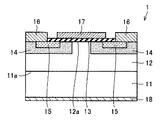
図1に、本発明の炭化ケイ素半導体装置の一例である縦型DiMOSFET(Double Implanted Metal Oxide Semiconductor Field Effect Transistor)の一例の模式的な断面図を示す。
<Embodiment 1>
FIG. 1 shows a schematic cross-sectional view of an example of a vertical DiMOSFET (Double Implanted Metal Oxide Semiconductor Field Effect Transistor) which is an example of the silicon carbide semiconductor device of the present invention.
図1に示す炭化ケイ素半導体装置1は、たとえばn型でポリタイプが4H−SiCの炭化ケイ素からなる基板11と、基板11の表面11a上に形成されたn型の炭化ケイ素からなる半導体層12と、半導体層12の表面12a内に形成されたp型領域である第2導電型不純物拡散層14と、第2導電型不純物拡散層14の表面内(半導体層12の表面12a内でもある)に形成されたn型領域である第1導電型不純物拡散層15と、半導体層12の表面12aに接するようにして形成された絶縁膜13と、半導体層12の表面12aの絶縁膜13の形成領域以外の領域に形成されたソース電極16と、絶縁膜13の表面上に形成されたゲート電極17と、基板11の裏面に形成されたドレイン電極18とを備えている。
A silicon carbide semiconductor device 1 shown in FIG. 1 includes, for example, a
ここで、半導体層12が形成される基板11の表面11aは、{0001}面に対して50°以上65°以下の範囲内で傾いている結晶面となっている。
Here, the
また、半導体層12としては、たとえば、基板11よりもn型不純物濃度の低いn型の炭化ケイ素からなる層などを用いることができる。また、半導体層12の表面12aも{0001}面に対して50°以上65°以下の範囲内で傾いている結晶面となっている。
Further, as the
また、絶縁膜13としては、たとえば、ドライ酸化(熱酸化)などによって形成された酸化膜などを用いることができる。なお、絶縁膜13は、1層の構造のものに限られず、2層以上の構造のものであってもよい。
As the
また、第2導電型不純物拡散層14としては、たとえば、半導体層12の表面12a内に第2導電型不純物としてのp型不純物を拡散させることによって形成したp型領域などを用いることができる。ここで、第2導電型不純物としてのp型不純物としては、たとえばアルミニウム、ボロンなどを用いることができる。また、第2導電型不純物拡散層14の表面内における第1導電型不純物拡散層15の形成領域以外の領域の少なくとも一部に第2導電型不純物拡散層14よりも高濃度の第2導電型不純物としてのp型不純物を含むp+型領域が形成されていてもよい。
In addition, as the second conductivity type
また、第1導電型不純物拡散層15としては、たとえば、半導体層12の表面12a内に第1導電型不純物としてのn型不純物を拡散させることによって形成したn型領域などを用いることができる。また、第1導電型不純物拡散層15中の第1導電型不純物としてのn型不純物濃度は、半導体層12中の第1導電型不純物としてのn型不純物濃度よりも高くすることができる。ここで、第1導電型不純物としてのn型不純物としては、たとえば窒素、リンなどを用いることができる。
In addition, as the first conductivity type
また、ソース電極16、ゲート電極17およびドレイン電極18はそれぞれ、たとえば、従来から公知の金属などを用いることができる。
The
また、図1に示す炭化ケイ素半導体装置1においては、半導体層12と絶縁膜13との界面から10nm以内の領域における窒素濃度の最大値は1×1021cm-3以上となっている。ここで、半導体層12と絶縁膜13との界面から10nm以内の領域とは、半導体層12と絶縁膜13との界面からその界面に対して垂直に半導体層12側に10nmだけ進向した領域と、半導体層12と絶縁膜13との界面からその界面に対して垂直に絶縁膜13側に10nmだけ進向した領域とを足し合わせた領域である。
In the silicon carbide semiconductor device 1 shown in FIG. 1, the maximum value of the nitrogen concentration in the region within 10 nm from the interface between the
図2に、図1に示す炭化ケイ素半導体装置1をゲート電極17側から見た模式的な平面図を示す。ここで、ソース電極16の表面およびゲート電極17の表面はそれぞれ<−2110>方向にストライプ状に伸びるようにして形成されており、<−2110>方向に直交する方向にソース電極16とゲート電極17とが交互に配列されている。また、2つのソース電極16の間に1つのゲート電極17が配置され、ソース電極16とゲート電極17との間の間隙から絶縁膜13の表面が露出している。このように、ソース電極16の表面がストライプ状である場合には、後述するように半導体層12の表面12a内において<−2110>方向に直交する方向±10°の範囲内にチャネル方向を形成しやすい傾向にある。なお、本発明において、チャネル方向とは、半導体層12の表面12a内においてキャリアが移動する方向を意味する。
FIG. 2 is a schematic plan view of silicon carbide semiconductor device 1 shown in FIG. 1 viewed from the
ここで、上記構成の炭化ケイ素半導体装置1のチャネル方向は、半導体層12の表面12a内において<−2110>方向に直交する方向±10°の範囲内に含まれるように形成される。
Here, the channel direction of silicon carbide semiconductor device 1 having the above-described configuration is formed to be included in the range of ± 10 ° in the direction orthogonal to the <−2110> direction in
以下、上記構成の炭化ケイ素半導体装置1の製造方法の一例について説明する。まず、図3の模式的断面図に示すように、{0001}面に対して50°以上65°以下の範囲内で傾いている結晶面からなる表面11aを有する炭化ケイ素(4H−SiC)からなる基板11を準備する。
Hereinafter, an example of the manufacturing method of the silicon carbide semiconductor device 1 having the above-described configuration will be described. First, as shown in the schematic cross-sectional view of FIG. 3, from silicon carbide (4H—SiC) having a
ここで、上記の表面11aを有する基板11は、たとえば、図4の模式的斜視図に示すように、[0001]方向(c軸方向)に結晶成長して{0001}面が露出したn型の炭化ケイ素結晶インゴッド10を{0001}面に対する角度α°が50°以上65°以下となる方向にスライスして、{0001}面に対して50°以上65°以下の角度で傾いている結晶面(図4の斜線部分)を露出させることなどにより形成することができる。
Here, as shown in the schematic perspective view of FIG. 4, for example, the
また、{0001}面に対して50°以上65°以下の範囲内で傾いている基板11の表面11aは、たとえば、図5の模式的断面図に示すように、{03−38}面に対して±5°の範囲内で傾いている結晶面でもあることが好ましい。基板11の表面11aが{03−38}面に対して±5°の範囲内で傾いている結晶面である場合には、炭化ケイ素半導体装置1のチャネル移動度などの電気的特性が向上する傾向にある。また、炭化ケイ素半導体装置1のチャネル移動度などの電気的特性をさらに向上させる観点からは、基板11の表面11aが{03−38}面に対して±3°の範囲内で傾いている結晶面であることがより好ましく、基板11の表面11aが{03−38}面であることが最も好ましい。なお、{03−38}面に対して±5°の範囲内で傾いている結晶面および{03−38}面に対して±3°の範囲内で傾いている結晶面にはそれぞれ{03−38}面が含まれることは言うまでもない。
Further, the
次に、図6の模式的断面図に示すように、基板11の表面11a上に半導体層12を形成する。
Next, as shown in the schematic cross-sectional view of FIG. 6, the
ここで、半導体層12は、たとえば、基板11の表面11a上に、基板11よりも低濃度のn型不純物を有するn型の炭化ケイ素からなる半導体層12をエピタキシャル成長させることなどにより形成することができる。上記のエピタキシャル成長により半導体層12を形成した場合には、基板11の表面11aの結晶面を半導体層12の表面12aに引き継がせることができるため、半導体層12の表面12aを{0001}面に対して50°以上65°以下の範囲内で傾いている結晶面とすることができる。
Here, the
また、上記と同様の理由により、半導体層12の表面12aは、{03−38}面に対して±5°の範囲内で傾いている結晶面であることが好ましく、{03−38}面に対して±3°の範囲内で傾いている結晶面であることがより好ましく、{03−38}面であることが最も好ましい。なお、ここでも、{03−38}面に対して±5°の範囲内で傾いている結晶面および{03−38}面に対して±3°の範囲内で傾いている結晶面にはそれぞれ{03−38}面が含まれることは言うまでもない。
For the same reason as described above, the
次に、図7の模式的平面図に示すように、半導体層12の表面12a内において<−2110>方向に直交する方向を調査する。
Next, as shown in the schematic plan view of FIG. 7, the direction orthogonal to the <−2110> direction in the
ここで、半導体層12の表面12a内における<−2110>方向に直交する方向は、たとえば、半導体層12に含まれる欠陥に基づいて調査することが可能である。すなわち、炭化ケイ素半導体装置1の製造工程においては、半導体層12の一定の箇所に欠陥が形成されることがあるため、半導体層12の一定の箇所に形成される欠陥の位置を基準とすることにより、半導体層12の表面12a内において<−2110>方向に直交する方向を特定することができる。また、半導体層12の表面モフォロジーに基づいても半導体層12の表面12a内において<−2110>方向に直交する方向を特定することができる。
Here, the direction orthogonal to the <−2110> direction in the
次に、図8の模式的断面図に示すように、半導体層12の表面12a内に第2導電型不純物拡散層14を形成する。この例においては、第2導電型不純物拡散層14は、<−2110>方向に伸びるストライプ状に形成されるが、この形状に限定されるものではない。
Next, as shown in the schematic cross-sectional view of FIG. 8, the second conductivity type
ここで、第2導電型不純物拡散層14は、たとえば、半導体層12の表面12a内の第2導電型不純物拡散層14の形成領域以外の領域にイオン注入防止マスクを設置した後に、第2導電型不純物としてのp型不純物のイオンを半導体層12の表面12aにイオン注入することなどにより形成することができる。なお、イオン注入防止マスクとしては、たとえば、フォトリソグラフィおよびエッチングを用いてパターンニングされた酸化膜などを用いることができる。
Here, the second conductivity type
次に、図9の模式的断面図に示すように、上記のように形成された第2導電型不純物拡散層14の表面内に第1導電型不純物拡散層15を形成する。この例においては、第1導電型不純物拡散層15も、<−2110>方向に伸びるストライプ状に形成されるが、この形状に限定されるものではない。
Next, as shown in the schematic cross-sectional view of FIG. 9, the first conductivity type
ここで、第1導電型不純物拡散層15は、たとえば、半導体層12の表面12a内の第1導電型不純物拡散層15の形成領域以外の領域にイオン注入防止マスクを設置した後に、第1導電型不純物としてのn型不純物のイオンを半導体層12の表面12aにイオン注入することなどにより形成することができる。なお、イオン注入防止マスクとしては、ここでも、たとえば、フォトリソグラフィおよびエッチングを用いてパターンニングされた酸化膜などを用いることができる。
Here, the first conductivity type
次に、上記のように第2導電型不純物拡散層14および第1導電型不純物拡散層15の形成後の半導体層12について活性化アニール処理を行なう。これにより、上記でイオン注入された第2導電型不純物拡散層14中の第2導電型不純物としてのp型不純物および第1導電型不純物拡散層15中の第1導電型不純物としてのn型不純物を活性化させることができる。
Next, activation annealing is performed on the
ここで、活性化アニール処理は、たとえばアルゴンガスの雰囲気中で、第2導電型不純物拡散層14および第1導電型不純物拡散層15の形成後の半導体層12をたとえば1700℃程度の温度で30分間程度加熱することなどにより行なうことができる。
Here, the activation annealing treatment is performed at a temperature of about 1700 ° C., for example, on the
次に、図10の模式的断面図に示すように、第2導電型不純物拡散層14および第1導電型不純物拡散層15の形成後の半導体層12の表面12aの全面に接する絶縁膜13を形成する。
Next, as shown in the schematic cross-sectional view of FIG. 10, the insulating
ここで、絶縁膜13としては、たとえば、ドライ酸化(熱酸化)などにより形成された酸化膜などを用いることができる。なお、ドライ酸化(熱酸化)は、たとえば空気中で、上記のように形成された第2導電型不純物拡散層14および第1導電型不純物拡散層15が形成された半導体層12の表面12aをたとえば1200℃程度の温度で30分間程度加熱することなどにより行なうことができる。
Here, as the insulating
次に、上記の絶縁膜13の形成後の半導体層12について、窒素アニール処理を行なう。これにより、半導体層12と絶縁膜13との界面から10nm以内の領域における窒素濃度の最大値が1×1021cm-3以上となるように窒素濃度を調整する。
Next, a nitrogen annealing process is performed on the
ここで、上記の窒素アニール処理は、たとえば、一酸化窒素(NO)ガスなどの窒素を含有するガスの雰囲気中で上記の絶縁膜13形成後の半導体層12をたとえば1100℃程度の温度で120分間程度加熱して行なうことにより、半導体層12と絶縁膜13との界面から10nm以内の領域における窒素濃度の最大値を1×1021cm-3以上とすることができる。
Here, the above-mentioned nitrogen annealing treatment is performed, for example, by subjecting the
また、上記の窒素アニール処理後の半導体層12については、たとえばアルゴンガスなどの不活性ガスの雰囲気中でさらに不活性ガスアニール処理を行なうことが好ましい。上記の窒素アニール処理後の半導体層12に上記の不活性ガスアニール処理を行なった場合には、炭化ケイ素半導体装置1について、高いチャネル移動度を再現性良く実現することができる傾向が大きくなる。
Further, it is preferable that the
ここで、上記の不活性ガスアニール処理は、たとえばアルゴンガスの雰囲気中で、上記の窒素アニール処理後の半導体層12を、たとえば1100℃程度の温度で60分間程度加熱することにより行なうことができる。
Here, the above-described inert gas annealing treatment can be performed by heating the
次に、図11の模式的断面図に示すように、上記のように形成された絶縁膜13の一部を除去して絶縁膜13のパターンニングを行なう。
Next, as shown in the schematic cross-sectional view of FIG. 11, a part of the insulating
ここで、絶縁膜13のパターンニングは、たとえば図12の模式的平面図に示すように、半導体層12の表面12a内の<−2110>方向に直交する方向±10°の範囲内にチャネル方向が含まれるように行なわれる。すなわち、絶縁膜13のパターンニングは、チャネル方向が、半導体層12の表面12a内の<−2110>方向に直交する方向−10°から<−2110>方向に直交する方向+10°の範囲内のいずれかの方向と平行となるように行なわれる。
Here, the patterning of the insulating
また、絶縁膜13の一部の除去は、たとえば、フォトリソグラフィおよびエッチングにより絶縁膜13の除去部分が露出するようにパターンニングされたエッチングマスクを絶縁膜13の表面上に形成した後に、絶縁膜13の露出部分をエッチングで除去することなどにより形成することができる。
The insulating
次に、図1に示すように、絶縁膜13の除去部分から露出した半導体層12の表面12a内の第1導電型不純物拡散層15の表面に接するようにソース電極16を形成する。
Next, as shown in FIG. 1, the
ここで、ソース電極16は、たとえば、上記の絶縁膜13のエッチング後に露出した半導体層12の表面12aおよび上記のエッチングマスクの表面上にたとえばニッケルなどの金属からなる導電膜をたとえばスパッタ法などにより形成した後に上記のエッチングマスクを除去することにより形成することができる。すなわち、エッチングマスクの表面上に形成された導電膜がエッチングマスクとともに除去(リフトオフ)され、半導体層12の表面12a上に形成された導電膜のみがソース電極16として残ることになる。
Here, the
また、上記のソース電極16の形成後の半導体層12については、アロイ化のための熱処理を行なうことが好ましい。
In addition, it is preferable that the
ここで、アロイ化のための熱処理としては、たとえばアルゴンガスなどの不活性ガスの雰囲気中で、上記のソース電極16の形成後の半導体層12をたとえば950℃程度の温度で2分間程度加熱することにより行なうことができる。
Here, as the heat treatment for alloying, the
次に、図1に示すように、絶縁膜13の表面上にゲート電極17を形成する。ここで、ゲート電極17は、たとえば、絶縁膜13の表面およびソース電極16の表面の全面をそれぞれ覆うようにして、フォトリソグラフィおよびエッチングなどによりゲート電極17の形成部分に開口部を有するレジストマスクを形成し、そのレジストマスクの表面およびレジストマスクの開口部から露出している絶縁膜13の表面上にたとえばアルミニウムなどの金属からなる導電膜をたとえばスパッタ法などにより形成した後に上記のレジストマスクを除去することにより形成することができる。すなわち、レジストマスクの表面上に形成された導電膜がレジストマスクとともに除去(リフトオフ)され、絶縁膜13の表面上に形成された導電膜のみがゲート電極17として残ることになる。
Next, as shown in FIG. 1, a
次に、図1に示すように、基板11の裏面上にドレイン電極18を形成する。ここで、ドレイン電極18は、たとえば、基板11の裏面上にたとえばニッケルなどの金属からなる導電膜をたとえばスパッタ法などにより形成することができる。
Next, as shown in FIG. 1, the
以上により、図1に示す構成の炭化ケイ素半導体装置1を製造することができる。
なお、本発明の炭化ケイ素半導体装置1においては、たとえば図13の模式的平面図に示すように、ソース電極16の表面をハニカム状に形成し、ソース電極16の外周を取り囲む一部の領域を除いた領域をゲート電極17として形成することもできる。
Thus, silicon carbide semiconductor device 1 having the configuration shown in FIG. 1 can be manufactured.
In silicon carbide semiconductor device 1 of the present invention, for example, as shown in the schematic plan view of FIG. 13, the surface of
上記のように、ソース電極16の表面をハニカム状に形成した場合には、個々のソース電極16の表面は六角形状に形成されることになるが、なかでも正六角形状に形成されることが好ましい。個々のソース電極16の表面を正六角形状に形成した場合には、<−2110>方向に直交する方向±10°の範囲内にチャネル方向を形成しやすくなるとともに、同一の大きさの基板11を用いた場合でも炭化ケイ素半導体装置1の形成可能数を増加させることができるため、高いチャネル移動度を有する炭化ケイ素半導体装置1をより再現性良く、かつより高い製造効率で作製することができる傾向にある。
As described above, when the surface of the
なお、図13に示す構成のソース電極16およびゲート電極17を有する炭化ケイ素半導体装置1のその他の構成は上記と同様とすることができる。
The other configuration of silicon carbide semiconductor device 1 having
上記で説明した構成の炭化ケイ素半導体装置1において、たとえば、ソース電極16に負電圧を印加し、ゲート電極17およびドレイン電極18に正電圧を印加した場合には、ソース電極16から注入されたキャリア(上記の例では電子)は、第1導電型不純物拡散層15の表面、第2導電型不純物拡散層14の表面、半導体層12の内部、基板11の内部を通ってドレイン電極18まで移動することになる。
In silicon carbide semiconductor device 1 having the configuration described above, for example, when a negative voltage is applied to source
なお、ソース電極16に負電圧を印加し、ドレイン電極18に正電圧を印加した場合でも、ゲート電極17に正電圧を印加しない場合には、ソース電極16から注入されたキャリア(上記の例では電子)の第2導電型不純物拡散層14の表面内における移動を制限することができる。
Even when a negative voltage is applied to the
上記構成の炭化ケイ素半導体装置1においては、たとえば、n型の炭化ケイ素(4H−SiC)の{0001}面に対して50°以上65°以下の範囲内で傾いている基板11の表面11a上に基板11よりも低濃度の第1導電型不純物としてのn型不純物を含むn型の炭化ケイ素からなる半導体層12をエピタキシャル成長により形成することができる。このような構成とした場合には、半導体層12の表面12a({0001}面に対して50°以上65°以下の範囲内で傾いている結晶面)をキャリアが移動するチャネルに利用することができるため、{0001}面をチャネルに利用した場合と比べて、高いキャリア移動度(チャネル移動度)を得ることができる。
In silicon carbide semiconductor device 1 having the above configuration, for example, on
また、上記で説明した構成の炭化ケイ素半導体装置1においては、たとえば図14に示すように、半導体層12と絶縁膜13との界面から10nm以内の領域における窒素濃度の最大値が1×1021cm-3以上となっている。したがって、本発明の炭化ケイ素半導体装置1においては、半導体層12と絶縁膜13との界面において絶縁膜13をドライ酸化(熱酸化)などによって形成した場合に発生する界面準位を低減することができることから、特に絶縁膜13の直下のチャネル(絶縁膜13に接する半導体層12の表面12a部分であって、第1導電型不純物拡散層15と半導体層12との間の第2導電型不純物拡散層14の表面部分)におけるキャリア移動度(チャネル移動度)を安定して向上させることができる。
In silicon carbide semiconductor device 1 having the above-described configuration, for example, as shown in FIG. 14, the maximum value of the nitrogen concentration in a region within 10 nm from the interface between
なお、図14には、上記で説明した構成の炭化ケイ素半導体装置1における絶縁膜13と半導体層12との界面近傍における窒素濃度の分布の一例が示されている。ここで、図14において、縦軸は窒素濃度(cm-3)を示し、横軸は絶縁膜13と半導体層12との界面からの距離(nm)を示している。また、図14において、横軸の距離(nm)が0(nm)の箇所が絶縁膜13と半導体層12との界面を意味しており、横軸の距離(nm)が0(nm)の箇所から左側に進むにつれて絶縁膜13側に進向することを意味し、横軸の距離(nm)が0(nm)の箇所から右側に進むにつれて半導体層12側に進向することを意味している。
FIG. 14 shows an example of the distribution of nitrogen concentration in the vicinity of the interface between insulating
さらに、上記で説明した構成の炭化ケイ素半導体装置1は、半導体層12の表面12a内において<−2110>方向に直交する方向±10°の範囲内にチャネル方向を有しているため、そのチャネル方向におけるキャリアの移動がスムーズになり、そのチャネル方向におけるキャリア移動度および電流特性を改善することができるため、炭化ケイ素半導体装置1のオン抵抗を低減することができる。
Furthermore, since silicon carbide semiconductor device 1 having the above-described configuration has a channel direction within a range of ± 10 ° in a direction orthogonal to the <−2110> direction in
図15に、上記で説明した構成の炭化ケイ素半導体装置1における半導体層12の表面12a({0001}面に対して50°以上65°以下の範囲内で傾いている結晶面)内における<−2110>方向に対する角度(°)とチャネル移動度(相対値)との関係の一例を示す。図15において、縦軸はチャネル移動度(相対値)を示し、横軸は半導体層12の表面12a内における<−2110>方向に対する角度(°)を示している。なお、図15の横軸の角度(°)は、<−2110>方向に対する傾きの方向は問わないため、たとえば、横軸の80°は<−2110>方向に対して+80°傾いている方向および−80°傾いている方向のいずれも意味している。
FIG. 15 shows the <− in the
なお、図15の縦軸のチャネル移動度(相対値)は、半導体層12の表面12a内の<−2110>方向に直交する方向のチャネル移動度を1としたときの相対値で表わされている。また、図15の横軸の角度(°)の90°の箇所が半導体層12の表面12a内における<−2110>方向に直交する方向を示している。
Note that the channel mobility (relative value) on the vertical axis in FIG. 15 is expressed as a relative value when the channel mobility in the direction orthogonal to the <−2110> direction in the
図15に示すように、半導体層12の表面12a内において<−2110>方向に対する角度が90°の方向(<−2110>方向に直交する方向)にチャネル方向がある場合に最もチャネル移動度が高くなり、半導体層12の表面12a内における<−2110>方向に直交する方向からのずれが大きくなるにつれてチャネル移動度が低下していく傾向にあることがわかる。なお、図15に示す傾向は、半導体層12の表面12aが{0001}面に対して50°以上65°以下の範囲内で傾いている結晶面のいずれについても成立する。
As shown in FIG. 15, in the
したがって、高いチャネル移動度を実現する観点からは、チャネル方向が、半導体層12の表面12a内の<−2110>方向に直交する方向となる場合(すなわち、<−2110>方向に直交する方向±0°の場合)が最も好ましいと考えられる。
Therefore, from the viewpoint of realizing high channel mobility, the channel direction is a direction orthogonal to the <−2110> direction in the
しかしながら、図15に示すように、半導体層12の表面12a内における<−2110>方向に対する角度が80°以上90°以下の方向(すなわち、<−2110>方向に直交する方向±10°の範囲内の方向)にチャネル方向が存在する場合には、チャネル移動度(相対値)が0.99よりも高くなるため、炭化ケイ素半導体装置1のチャネル移動度が多少ばらついた場合でも、チャネル移動度が大きく低下することは考えにくい。
However, as shown in FIG. 15, the angle with respect to the <−2110> direction in the
したがって、半導体層12の表面12a内における<−2110>方向に直交する方向±10°の範囲内にチャネル方向を有する本発明の炭化ケイ素半導体装置1においては、高いチャネル移動度を再現性良く実現することができる。また、本発明の炭化ケイ素半導体装置1において、高いチャネル移動度を再現性良く実現するためには、半導体層12の表面12a内の<−2110>方向に直交する方向にチャネル方向を形成することが最も好ましいことは上述したとおりである。
Therefore, in the silicon carbide semiconductor device 1 of the present invention having a channel direction within a range of ± 10 ° in a direction perpendicular to the <−2110> direction in the
なお、上記においては、第1導電型をn型とし、第2導電型をp型とした場合について説明したが、本発明においては、上記の炭化ケイ素半導体装置1の構成において、第1導電型をp型とし、第2導電型をn型とした構成としてもよい。 In the above description, the case where the first conductivity type is n-type and the second conductivity type is p-type has been described. However, in the present invention, in the configuration of the silicon carbide semiconductor device 1 described above, the first conductivity-type is used. May be p-type and the second conductivity type may be n-type.
<実施の形態2>
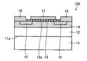
図16に、本発明の炭化ケイ素半導体装置の一例である横型MOSFET(Metal Oxide Semiconductor Field Effect Transistor)の一例の模式的な断面図を示す。
<Embodiment 2>
FIG. 16 is a schematic cross-sectional view of an example of a lateral MOSFET (Metal Oxide Semiconductor Field Effect Transistor) that is an example of the silicon carbide semiconductor device of the present invention.
図16に示す炭化ケイ素半導体装置100は、たとえばn型でポリタイプが4H−SiCの炭化ケイ素からなる基板11と、基板11の表面11a上に形成されたn型の炭化ケイ素からなる半導体層12と、半導体層12の表面12a内に形成されたp型領域である第2導電型不純物拡散層14と、第2導電型不純物拡散層14の表面内(半導体層12の表面12a内でもある)に形成されたn型領域である第1導電型不純物拡散層15と、半導体層12の表面12aに接するようにして形成された絶縁膜13と、半導体層12の表面12aの絶縁膜13の形成領域以外の領域に形成されたソース電極16およびドレイン電極18と、半導体層12の表面12aの絶縁膜13の表面上に形成されたゲート電極17とを備えている。
A silicon
ここでも、半導体層12が形成される基板11の表面11aは、{0001}面に対して50°以上65°以下の範囲内で傾いている結晶面となっている。また、半導体層12の表面12aも{0001}面に対して50°以上65°以下の範囲内で傾いている結晶面となっている。
Also here, the
また、絶縁膜13としては、たとえば、ドライ酸化(熱酸化)などによって形成された酸化膜などを用いることができる。なお、絶縁膜13は、1層の構造のものに限られず、2層以上の構造のものであってもよい。
As the insulating
また、第2導電型不純物拡散層14としては、たとえば、半導体層12の表面12a内に第2導電型不純物としてのp型不純物を拡散させることによって形成したp型領域などを用いることができる。また、第2導電型不純物拡散層14の表面内における第1導電型不純物拡散層15の形成領域以外の領域の少なくとも一部に第2導電型不純物拡散層14よりも高濃度の第2導電型不純物としてのp型不純物を含むp+型領域が形成されていてもよい。
In addition, as the second conductivity type
また、第1導電型不純物拡散層15としては、たとえば、半導体層12の表面12a内に第1導電型不純物としてのn型不純物を拡散させることによって形成したn型領域などを用いることができる。また、第1導電型不純物拡散層15中の第1導電型不純物としてのn型不純物濃度は、半導体層12中の第1導電型不純物としてのn型不純物濃度よりも高くすることができる。ここで、第1導電型不純物としてのn型不純物としては、たとえば窒素、リンなどを用いることができる。
In addition, as the first conductivity type
また、図16に示す炭化ケイ素半導体装置100においても、半導体層12と絶縁膜13との界面から10nm以内の領域における窒素濃度の最大値は1×1021cm-3以上となっている。ここでも、半導体層12と絶縁膜13との界面から10nm以内の領域とは、半導体層12と絶縁膜13との界面からその界面に対して垂直に半導体層12側に10nmだけ進向した領域と、半導体層12と絶縁膜13との界面からその界面に対して垂直に絶縁膜13側に10nmだけ進向した領域とを足し合わせた領域である。
Also in the silicon
図17に、図16に示す炭化ケイ素半導体装置100をゲート電極17側から見た模式的な平面図を示す。ここで、ソース電極16の表面、ゲート電極17の表面およびドレイン電極18の表面はそれぞれ<−2110>方向にストライプ状に伸びるようにして形成されており、<−2110>方向に直交する方向にソース電極16、ゲート電極17およびドレイン電極18がこの順序で配列されている。
FIG. 17 is a schematic plan view of silicon
また、ソース電極16とドレイン電極18との間に1つのゲート電極17が配置されており、ソース電極16とゲート電極17との間の間隙およびゲート電極17とドレイン電極18との間の間隙のそれぞれから絶縁膜13の表面が露出している。
One
このように、ソース電極16の表面、ゲート電極17の表面およびドレイン電極18の表面がストライプ状である場合には、後述するように半導体層12の表面12a内において<−2110>方向に直交する方向±10°の範囲内にチャネル方向を形成しやすい傾向にある。なお、本発明において、チャネル方向とは、半導体層12の表面12a内においてキャリアが移動する方向を意味する。
Thus, when the surface of the
ここでも、上記構成の炭化ケイ素半導体装置100のチャネル方向は、半導体層12の表面12a内において<−2110>方向に直交する方向±10°の範囲内に含まれるように形成される。
Also in this case, the channel direction of silicon
以下、上記構成の炭化ケイ素半導体装置100の製造方法の一例について説明する。まず、図3の模式的断面図に示すように、{0001}面に対して50°以上65°以下の範囲内で傾いている結晶面からなる表面11aを有する炭化ケイ素(4H−SiC)からなる基板11を準備する。
Hereinafter, an example of a method for manufacturing silicon
ここで、上記の表面11aを有する基板11は、たとえば、図4の模式的斜視図に示すように、[0001]方向(c軸方向)に結晶成長して{0001}面が露出したn型の炭化ケイ素結晶インゴッド10を{0001}面に対する角度α°が50°以上65°以下となる方向にスライスして、{0001}面に対して50°以上65°以下の角度で傾いている結晶面(図4の斜線部分)を露出させることなどにより形成することができる。
Here, as shown in the schematic perspective view of FIG. 4, for example, the
また、{0001}面に対して50°以上65°以下の範囲内で傾いている基板11の表面11aは、たとえば、図5の模式的断面図に示すように、{03−38}面に対して±5°の範囲内で傾いている結晶面でもあることが好ましい。基板11の表面11aが{03−38}面に対して±5°の範囲内で傾いている結晶面である場合には、炭化ケイ素半導体装置100のチャネル移動度などの電気的特性が向上する傾向にある。また、炭化ケイ素半導体装置100のチャネル移動度などの電気的特性をさらに向上させる観点からは、基板11の表面11aが{03−38}面に対して±3°の範囲内で傾いている結晶面であることがより好ましく、基板11の表面11aが{03−38}面であることが最も好ましい。なお、{03−38}面に対して±5°の範囲内で傾いている結晶面および{03−38}面に対して±3°の範囲内で傾いている結晶面にはそれぞれ{03−38}面が含まれることは言うまでもない。
Further, the
次に、図6の模式的断面図に示すように、基板11の表面11a上に半導体層12を形成する。
Next, as shown in the schematic cross-sectional view of FIG. 6, the
ここで、半導体層12は、たとえば、基板11の表面11a上に、基板11よりも低濃度のn型不純物を有するn型の炭化ケイ素からなる半導体層12をエピタキシャル成長させることなどにより形成することができる。上記のエピタキシャル成長により半導体層12を形成した場合には、基板11の表面11aの結晶面を半導体層12の表面12aに引き継がせることができるため、半導体層12の表面12aを{0001}面に対して50°以上65°以下の範囲内で傾いている結晶面とすることができる。
Here, the
また、上記と同様の理由により、半導体層12の表面12aは、{03−38}面に対して±5°の範囲内で傾いている結晶面であることが好ましく、{03−38}面に対して±3°の範囲内で傾いている結晶面であることがより好ましく、{03−38}面であることが最も好ましい。なお、ここでも、{03−38}面に対して±5°の範囲内で傾いている結晶面および{03−38}面に対して±3°の範囲内で傾いている結晶面にはそれぞれ{03−38}面が含まれることは言うまでもない。
For the same reason as described above, the
次に、図7の模式的平面図に示すように、半導体層12の表面12a内において<−2110>方向に直交する方向を調査する。
Next, as shown in the schematic plan view of FIG. 7, the direction orthogonal to the <−2110> direction in the
ここで、半導体層12の表面12a内における<−2110>方向に直交する方向は、たとえば、半導体層12に含まれる欠陥に基づいて調査することが可能である。すなわち、炭化ケイ素半導体装置100の製造工程においては、半導体層12の一定の箇所に欠陥が形成されることがあるため、半導体層12の一定の箇所に形成される欠陥の位置を基準とすることにより、半導体層12の表面12a内において<−2110>方向に直交する方向を特定することができる。また、半導体層12の表面モフォロジーに基づいても半導体層12の表面12a内において<−2110>方向に直交する方向を特定することができる。
Here, the direction orthogonal to the <−2110> direction in the
次に、図18の模式的断面図に示すように、半導体層12の表面12aの全面に第2導電型不純物拡散層14を形成する。
Next, as shown in the schematic cross-sectional view of FIG. 18, the second conductivity type
次に、図19の模式的断面図に示すように、上記のように形成された第2導電型不純物拡散層14の表面内の一部に第1導電型不純物拡散層15を形成する。この例においては、第1導電型不純物拡散層15は、<−2110>方向に伸びるストライプ状に形成されるが、この形状に限定されるものではない。
Next, as shown in the schematic cross-sectional view of FIG. 19, the first conductivity type
ここで、第1導電型不純物拡散層15は、たとえば、半導体層12の表面12a内の第1導電型不純物拡散層15の形成領域以外の領域にイオン注入防止マスクを設置した後に、第1導電型不純物としてのn型不純物のイオンを半導体層12の表面12aにイオン注入することなどにより形成することができる。なお、イオン注入防止マスクとしては、ここでも、たとえば、フォトリソグラフィおよびエッチングを用いてパターンニングされた酸化膜などを用いることができる。
Here, the first conductivity type
次に、上記のように第2導電型不純物拡散層14および第1導電型不純物拡散層15の形成後の半導体層12について活性化アニール処理を行なう。これにより、上記でイオン注入された第2導電型不純物拡散層14中の第2導電型不純物としてのp型不純物および第1導電型不純物拡散層15中の第1導電型不純物としてのn型不純物を活性化させることができる。
Next, activation annealing is performed on the
ここで、活性化アニール処理は、たとえばアルゴンガスの雰囲気中で、第2導電型不純物拡散層14および第1導電型不純物拡散層15の形成後の半導体層12をたとえば1700℃程度の温度で30分間程度加熱することなどにより行なうことができる。
Here, the activation annealing treatment is performed at a temperature of about 1700 ° C., for example, on the
次に、図20の模式的断面図に示すように、第2導電型不純物拡散層14および第1導電型不純物拡散層15の形成後の半導体層12の表面12aの全面に接する絶縁膜13を形成する。
Next, as shown in the schematic cross-sectional view of FIG. 20, the insulating
ここで、絶縁膜13としては、たとえば、ドライ酸化(熱酸化)などにより形成された酸化膜などを用いることができる。なお、ドライ酸化(熱酸化)は、たとえば空気中で、上記のように形成された第2導電型不純物拡散層14および第1導電型不純物拡散層15が形成された半導体層12の表面12aをたとえば1200℃程度の温度で30分間程度加熱することなどにより行なうことができる。
Here, as the insulating
次に、上記の絶縁膜13の形成後の半導体層12について、窒素アニール処理を行なう。これにより、半導体層12と絶縁膜13との界面から10nm以内の領域における窒素濃度の最大値が1×1021cm-3以上となるように窒素濃度を調整する。
Next, a nitrogen annealing process is performed on the
ここで、上記の窒素アニール処理は、たとえば、一酸化窒素(NO)ガスなどの窒素を含有するガスの雰囲気中で上記の絶縁膜13形成後の半導体層12をたとえば1100℃程度の温度で120分間程度加熱して行なうことにより、半導体層12と絶縁膜13との界面から10nm以内の領域における窒素濃度の最大値を1×1021cm-3以上とすることができる。
Here, the above-mentioned nitrogen annealing treatment is performed, for example, by subjecting the
また、上記の窒素アニール処理後の半導体層12については、たとえばアルゴンガスなどの不活性ガスの雰囲気中でさらに不活性ガスアニール処理を行なうことが好ましい。上記の窒素アニール処理後の半導体層12に上記の不活性ガスアニール処理を行なった場合には、炭化ケイ素半導体装置100について、高いチャネル移動度を再現性良く実現することができる傾向が大きくなる。
Further, it is preferable that the
ここで、上記の不活性ガスアニール処理は、たとえばアルゴンガスの雰囲気中で、上記の窒素アニール処理後の半導体層12を、たとえば1100℃程度の温度で60分間程度加熱することにより行なうことができる。
Here, the above-described inert gas annealing treatment can be performed by heating the
次に、図21の模式的断面図に示すように、上記のように形成された絶縁膜13の一部を除去して絶縁膜13のパターンニングを行なう。
Next, as shown in the schematic cross-sectional view of FIG. 21, a part of the insulating
ここで、絶縁膜13のパターンニングは、たとえば図12の模式的平面図に示すように、半導体層12の表面12a内の<−2110>方向に直交する方向±10°の範囲内にチャネル方向が含まれるように行なわれる。すなわち、絶縁膜13のパターンニングは、チャネル方向が、半導体層12の表面12a内の<−2110>方向に直交する方向−10°から<−2110>方向に直交する方向+10°の範囲内のいずれかの方向と平行となるように行なわれる。
Here, the patterning of the insulating
また、絶縁膜13の一部の除去は、たとえば、フォトリソグラフィおよびエッチングにより絶縁膜13の除去部分が露出するようにパターンニングされたエッチングマスクを絶縁膜13の表面上に形成した後に、絶縁膜13の露出部分をエッチングで除去することなどにより形成することができる。
The insulating
次に、図16に示すように、絶縁膜13の除去部分から露出した半導体層12の表面12a内の第1導電型不純物拡散層15の表面に接するようにソース電極16およびドレイン電極18を形成する。
Next, as shown in FIG. 16, the
ここで、ソース電極16およびドレイン電極18は、たとえば、上記の絶縁膜13のエッチング後に露出した半導体層12の表面12aおよび上記のエッチングマスクの表面上にたとえばニッケルなどの金属からなる導電膜をたとえばスパッタ法などにより形成した後に上記のエッチングマスクを除去することにより形成することができる。すなわち、エッチングマスクの表面上に形成された導電膜がエッチングマスクとともに除去(リフトオフ)され、半導体層12の表面12a上に形成された導電膜のみがソース電極16およびドレイン電極18として残ることになる。
Here, the
また、上記のソース電極16およびドレイン電極18の形成後の半導体層12については、アロイ化のための熱処理を行なうことが好ましい。
The
ここで、アロイ化のための熱処理としては、たとえばアルゴンガスなどの不活性ガスの雰囲気中で、上記のソース電極16およびドレイン電極18の形成後の半導体層12をたとえば950℃程度の温度で2分間程度加熱することにより行なうことができる。
Here, as the heat treatment for alloying, the
次に、図16に示すように、絶縁膜13の表面上にゲート電極17を形成する。ここで、ゲート電極17は、たとえば、絶縁膜13の表面、ソース電極16の表面およびドレイン電極18の表面の全面をそれぞれ覆うようにして、フォトリソグラフィおよびエッチングなどによりゲート電極17の形成部分に開口部を有するレジストマスクを形成し、そのレジストマスクの表面およびレジストマスクの開口部から露出している絶縁膜13の表面上にたとえばアルミニウムなどの金属からなる導電膜をたとえばスパッタ法などにより形成した後に上記のレジストマスクを除去することにより形成することができる。すなわち、レジストマスクの表面上に形成された導電膜がレジストマスクとともに除去(リフトオフ)され、絶縁膜13の表面上に形成された導電膜のみがゲート電極17として残ることになる。
Next, as shown in FIG. 16, a
以上により、図16に示す構成の炭化ケイ素半導体装置100を製造することができる。
Thus, silicon
上記で説明した構成の炭化ケイ素半導体装置100において、たとえば、ソース電極16に負電圧を印加し、ゲート電極17およびドレイン電極18に正電圧を印加した場合には、ソース電極16から注入されたキャリア(上記の例では電子)は、ソース電極16側の第1導電型不純物拡散層15の表面、第2導電型不純物拡散層14の表面およびドレイン電極18側の第1導電型不純物拡散層15の表面を通ってドレイン電極18まで移動することになる。
In silicon
なお、ソース電極16に負電圧を印加し、ドレイン電極18に正電圧を印加した場合でも、ゲート電極17に正電圧を印加しない場合には、ソース電極16から注入されたキャリア(上記の例では電子)の第2導電型不純物拡散層14の表面内における移動を制限することができる。
Even when a negative voltage is applied to the
上記構成の炭化ケイ素半導体装置100においては、たとえば、n型の炭化ケイ素(4H−SiC)の{0001}面に対して50°以上65°以下の範囲内で傾いている基板11の表面11a上に基板11よりも低濃度の第1導電型不純物としてのn型不純物を含むn型の炭化ケイ素からなる半導体層12をエピタキシャル成長により形成することができる。このような構成とした場合には、半導体層12の表面12a({0001}面に対して50°以上65°以下の範囲内で傾いている結晶面)をキャリアが移動するチャネルに利用することができるため、{0001}面をチャネルに利用した場合と比べて、高いキャリア移動度(チャネル移動度)を得ることができる。
In silicon
また、上記で説明した構成の炭化ケイ素半導体装置100においても、たとえば図14に示すように、半導体層12と絶縁膜13との界面から10nm以内の領域における窒素濃度の最大値が1×1021cm-3以上となっている。したがって、本発明の炭化ケイ素半導体装置100においては、半導体層12と絶縁膜13との界面において絶縁膜13をドライ酸化(熱酸化)などによって形成した場合に発生する界面準位を低減することができることから、特に絶縁膜13の直下のチャネル(絶縁膜13に接する半導体層12の表面12a部分(第2導電型不純物拡散層14の表面部分))におけるキャリア移動度(チャネル移動度)を安定して向上させることができる。
Also in silicon
さらに、上記で説明した構成の炭化ケイ素半導体装置100は、半導体層12の表面12a内において<−2110>方向に直交する方向±10°の範囲内にチャネル方向を有しているため、そのチャネル方向におけるキャリアの移動がスムーズになり、そのチャネル方向におけるキャリア移動度および電流特性を改善することができるため、炭化ケイ素半導体装置100のオン抵抗を低減することができる。
Furthermore, since silicon
また、上記で説明した構成の炭化ケイ素半導体装置100においても、たとえば図15に示すように、半導体層12の表面12a内において<−2110>方向に対する角度が90°の方向(<−2110>方向に直交する方向)にチャネル方向がある場合に最もチャネル移動度が高くなり、半導体層12の表面12a内における<−2110>方向に直交する方向からのずれが大きくなるにつれてチャネル移動度が低下していく傾向にある。
Also in silicon
したがって、上記で説明した構成の炭化ケイ素半導体装置100においても、高いチャネル移動度を実現する観点からは、チャネル方向が、半導体層12の表面12a内の<−2110>方向に直交する方向となる場合(すなわち、<−2110>方向に直交する方向±0°の場合)が最も好ましいと考えられる。
Therefore, also in silicon
しかしながら、上記で説明した構成の炭化ケイ素半導体装置100においても、図15に示すように、半導体層12の表面12a内における<−2110>方向に対する角度が80°以上90°以下の方向(すなわち、<−2110>方向に直交する方向±10°の範囲内の方向)にチャネル方向が存在する場合には、チャネル移動度(相対値)が0.99よりも高くなるため、炭化ケイ素半導体装置100のチャネル移動度が多少ばらついた場合でも、チャネル移動度が大きく低下することは考えにくい。
However, also in the silicon
したがって、半導体層12の表面12a内における<−2110>方向に直交する方向±10°の範囲内にチャネル方向を有する本発明の炭化ケイ素半導体装置100においては、高いチャネル移動度を再現性良く実現することができる。また、本発明の炭化ケイ素半導体装置100において、高いチャネル移動度を再現性良く実現するためには、半導体層12の表面12a内の<−2110>方向に直交する方向にチャネル方向を形成することが最も好ましいことは上述したとおりである。
Therefore, in the silicon
なお、本実施の形態においても、第1導電型をn型とし、第2導電型をp型とした場合について説明したが、本発明においては、上記の炭化ケイ素半導体装置100の構成において、第1導電型をp型とし、第2導電型をn型とした構成としてもよい。
In the present embodiment, the case where the first conductivity type is n-type and the second conductivity type is p-type has been described. However, in the present invention, in the configuration of silicon
また、本実施の形態における上記以外の説明は実施の形態1と同様であるため、その説明については省略する。 In addition, since the description other than the above in the present embodiment is the same as that in the first embodiment, the description thereof is omitted.
<実施例1>
(縦型DiMOSFETの作製)
実施例の縦型DiMOSFETとしての炭化ケイ素半導体装置を以下のようにして作製した。
<Example 1>
(Production of vertical DiMOSFET)
A silicon carbide semiconductor device as a vertical DiMOSFET of an example was manufactured as follows.
まず、図3に示すように、厚さが400μmのn型の炭化ケイ素結晶(4H−SiC)からなる基板11を用意した。ここで、基板11は、{0001}面に対して約55°の角度で傾いている結晶面である{03−38}面を表面11aとして有している。
First, as shown in FIG. 3, a
次に、図6に示すように、基板11の表面11a上に、n型不純物として窒素がドープされたn型の炭化ケイ素結晶からなる半導体層12(n型不純物濃度:5×1015cm-3)をCVD(Chemical Vapor Deposition)法により10μmの厚さでエピタキシャル成長させた。
Next, as shown in FIG. 6, on the
次に、図7に示すように、半導体層12の表面12a内において<−2110>方向に直交する方向を調査した。ここで、半導体層12の表面12a内における<−2110>方向に直交する方向は、半導体層12に形成された欠陥を基準にして特定した。
Next, as shown in FIG. 7, the direction orthogonal to the <−2110> direction in the
次に、図8に示すように、半導体層12の表面12a内に第2導電型不純物拡散層14(p型不純物濃度:1×1017cm-3)を形成した。ここで、第2導電型不純物拡散層14は、半導体層12の表面12a内の第2導電型不純物拡散層14の形成領域以外の領域にフォトリソグラフィおよびエッチングを用いてパターンニングされた酸化膜を形成し、その酸化膜をイオン注入防止マスクとして、p型不純物であるボロンをイオン注入することにより形成した。なお、第2導電型不純物拡散層14は、第2導電型不純物拡散層14の表面が正六角形状となるように形成された。
Next, as shown in FIG. 8, a second conductivity type impurity diffusion layer 14 (p-type impurity concentration: 1 × 10 17 cm −3 ) was formed in the
次に、図9に示すように、上記のように形成された第2導電型不純物拡散層14の表面内に、第1導電型不純物拡散層15(n型不純物濃度:5×1019cm-3)およびp+型領域(図示せず)(p型不純物濃度:3×1019cm-3)を形成した。ここで、第1導電型不純物拡散層15は、第1導電型不純物拡散層15の表面が正六角形状となるように形成され、p+型領域は、第1導電型不純物拡散層15のチャネルの形成側と反対側に接するようにして形成した。なお、第1導電型不純物拡散層15は、半導体層12の表面12a内の第1導電型不純物拡散層15の形成領域以外の領域にフォトリソグラフィおよびエッチングを用いてパターンニングされた酸化膜を形成し、その酸化膜をイオン注入防止マスクとしてn型不純物であるリンをイオン注入することにより形成した。また、p+型領域も、半導体層12の表面12a内のp+型領域の形成領域以外の領域にフォトリソグラフィおよびエッチングを用いてパターンニングされた酸化膜を形成し、その酸化膜をイオン注入防止マスクとしてp型不純物であるボロンをイオン注入することにより形成した。
Next, as shown in FIG. 9, the first conductivity type impurity diffusion layer 15 (n-type impurity concentration: 5 × 10 19 cm − is formed in the surface of the second conductivity type
次に、上記のように第2導電型不純物拡散層14、第1導電型不純物拡散層15およびp+型領域が形成された半導体層12をアルゴンガス雰囲気中で、1700℃で30分間加熱することにより活性化アニール処理を行なった。
Next, the second conductivity type
次に、図10に示すように、半導体層12の表面12aを空気中で1200℃で30分間加熱してドライ酸化(熱酸化)することにより、半導体層12の表面12aの全面に接する絶縁膜13を形成した。
Next, as shown in FIG. 10, the
次に、絶縁膜13の形成後の半導体層12を一酸化窒素(NO)ガス雰囲気中で1100℃で120分間加熱することによって窒素アニール処理を行なった。
Next, nitrogen annealing treatment was performed by heating the
次に、上記の窒素アニール処理後の半導体層12をアルゴンガス雰囲気中で1100℃で60分間加熱することによって不活性ガスアニール処理を行なった。
Next, an inert gas annealing process was performed by heating the
次に、チャネル方向が半導体層12の表面12a内の<−2110>方向に直交する方向となるように、上記のように形成された絶縁膜13の一部を除去して絶縁膜13のパターンニングを行なった。ここで、絶縁膜13のパターンニングは、フォトリソグラフィおよびエッチングにより絶縁膜13の除去部分が露出するようにパターンニングされたエッチングマスクを絶縁膜13の表面上に形成した後に、絶縁膜13の露出部分をエッチングで除去することにより行なった。
Next, a part of the insulating
次に、絶縁膜13の除去部分から露出した第1導電型不純物拡散層15およびp+型領域(図示せず)の表面上に、図13に示すような正六角形状の表面を有するニッケルからなる0.1μmの厚さのソース電極16を形成した。
Next, nickel having a regular hexagonal surface as shown in FIG. 13 is formed on the surface of the first conductivity type
次に、上記のソース電極16の形成後の半導体層12をアルゴンガス雰囲気中で950℃で2分間加熱することによりアロイ化のための熱処理を行なった。
Next, heat treatment for alloying was performed by heating the
次に、絶縁膜13の表面上に、図13に示すような表面形状を有するアルミニウムからなる1μmの厚さのゲート電極17を形成した。
Next, a 1 μm-
次に、基板11の裏面の全面にニッケルからなる0.1μmの厚さのドレイン電極18を形成した。
Next, a
以上により、実施例の縦型DiMOSFETとしての炭化ケイ素半導体装置1を作製した。 Thus, silicon carbide semiconductor device 1 as a vertical DiMOSFET of the example was manufactured.
上記のようにして作製した実施例の縦型DiMOSFETとしての炭化ケイ素半導体装置1のチャネル長(半導体層12の表面12a内において隣り合うソース電極16の間の第1導電型不純物拡散層15と半導体層12との間の距離)は2μmとされた。
The channel length of the silicon carbide semiconductor device 1 as the vertical DiMOSFET of the embodiment manufactured as described above (the first conductivity type
また、比較として、チャネル方向を半導体層12の表面12a内の<−2110>方向としたこと以外は上記と同様にして比較例の縦型DiMOSFETとしての炭化ケイ素半導体装置を作製した。
For comparison, a silicon carbide semiconductor device as a vertical DiMOSFET of a comparative example was fabricated in the same manner as described above except that the channel direction was the <−2110> direction in the
(縦型DiMOSFETの評価)
上記のようにして作製した実施例と比較例の縦型DiMOSFETについて、半導体層12と絶縁膜13との界面近傍における窒素濃度の深さ方向での分布をSIMS(二次イオン質量分析)により測定した。
(Vertical DiMOSFET evaluation)
With respect to the vertical DiMOSFETs of Examples and Comparative Examples manufactured as described above, the distribution in the depth direction of the nitrogen concentration in the vicinity of the interface between the
その結果、実施例および比較例の縦型DiMOSFETのいずれにおいても、半導体層12と絶縁膜13との界面近傍における窒素濃度の最大値はそれぞれ1×1021cm-3以上であった。したがって、実施例と比較例の縦型DiMOSFETについてはそれぞれ、半導体層12と絶縁膜13との界面から10nm以内の領域における窒素濃度の最大値は1×1021cm-3以上となることが確認された。
As a result, in each of the vertical DiMOSFETs of the example and the comparative example, the maximum nitrogen concentration in the vicinity of the interface between the
また、実施例および比較例の縦型DiMOSFETについて、チャネル移動度を評価した。チャネル移動度の評価方法としては、以下の方法を用いた。まず、ソース−ドレイン間電圧VDS=0.1Vとした状態で、ゲート電圧VGを印加してソース−ドレイン間電流IDSを測定した(ゲート電圧依存性を測定した)。そして、gm=(δIDS)/(δVG)として、下記の式(1)により、チャネル移動度のゲート電圧に対する最大値を求め、その最大値をチャネル移動度として算出した。 Further, the channel mobility was evaluated for the vertical DiMOSFETs of the example and the comparative example. The following method was used as the channel mobility evaluation method. First, with the source-drain voltage VDS = 0.1 V, the gate voltage VG was applied to measure the source-drain current IDS (the gate voltage dependency was measured). Then, as gm = (δIDS) / (δVG), the maximum value of the channel mobility with respect to the gate voltage was obtained by the following equation (1), and the maximum value was calculated as the channel mobility.
チャネル移動度μ=gm×(L×d)/(W×ε×VDS) …(1)
なお、上記の式(1)において、Lはチャネル長を示し、dは絶縁膜13の厚さを示し、Wはチャネル幅を示し、εは絶縁膜13の誘電率を示している。
Channel mobility μ = gm × (L × d) / (W × ε × VDS) (1)
In the above equation (1), L represents the channel length, d represents the thickness of the insulating
その結果、実施例の縦型DiMOSFETのチャネル移動度は80cm2/Vsであり、比較例の縦型DiMOSFETのチャネル移動度は70cm2/Vsであった。 As a result, the channel mobility of the vertical DiMOSFET of the example was 80 cm 2 / Vs, and the channel mobility of the vertical DiMOSFET of the comparative example was 70 cm 2 / Vs.
したがって、実施例の縦型DiMOSFETのチャネル移動度は比較例の縦型DiMOSFETのチャネル移動度の約1.14倍であり、これに伴いソース−ドレイン間電流値が1.14倍となるため、オン抵抗が大幅に低減することが確認された。 Therefore, the channel mobility of the vertical DiMOSFET of the example is about 1.14 times the channel mobility of the vertical DiMOSFET of the comparative example, and accordingly, the source-drain current value is 1.14 times. It was confirmed that the on-resistance was greatly reduced.
よって、実施例の縦型DiMOSFETの構成によれば、製造上の問題でチャネル移動度が多少ばらついたとしても、チャネル移動度が大きく低下するとは考えられないため、高いチャネル移動度を再現性良く実現することができると考えられる。 Therefore, according to the configuration of the vertical DiMOSFET of the embodiment, even if the channel mobility varies somewhat due to a manufacturing problem, it is not considered that the channel mobility is greatly reduced. It can be realized.
<実施例2>
(横型MOSFETの作製)
実施例の横型MOSFETとしての炭化ケイ素半導体装置を以下のようにして作製した。
<Example 2>
(Production of lateral MOSFET)
A silicon carbide semiconductor device as a lateral MOSFET of the example was manufactured as follows.
まず、図3に示すように、厚さが400μmのn型の炭化ケイ素結晶(4H−SiC)からなる基板11を用意した。ここで、基板11は、{0001}面に対して約55°の角度で傾いている結晶面である{03−38}面を表面11aとして有している。
First, as shown in FIG. 3, a
次に、図6に示すように、基板11の表面11a上に、n型不純物として窒素がドープされたn型の炭化ケイ素結晶からなる半導体層12(n型不純物濃度:5×1015cm-3)をCVD(Chemical Vapor Deposition)法により10μmの厚さでエピタキシャル成長させた。
Next, as shown in FIG. 6, on the
次に、図7に示すように、半導体層12の表面12a内において<−2110>方向に直交する方向を調査した。ここで、半導体層12の表面12a内における<−2110>方向に直交する方向は、半導体層12の表面モフォロジーを基準にして特定した。
Next, as shown in FIG. 7, the direction orthogonal to the <−2110> direction in the
次に、図18に示すように、半導体層12の表面12aの全面に第2導電型不純物拡散層14(p型不純物濃度:1×1017cm-3)を形成した。
Next, as shown in FIG. 18, the second conductivity type impurity diffusion layer 14 (p-type impurity concentration: 1 × 10 17 cm −3 ) was formed on the
次に、図19に示すように、上記のように形成された第2導電型不純物拡散層14の表面内の一部に、第1導電型不純物拡散層15(n型不純物濃度:5×1019cm-3)およびp+型領域(図示せず)(p型不純物濃度:3×1019cm-3)を形成した。ここで、第1導電型不純物拡散層15は、第1導電型不純物拡散層15の表面がストライプ状となるように形成され、p+型領域は、第1導電型不純物拡散層15のチャネルの形成側と反対側に接するストライプ状に形成した。なお、第1導電型不純物拡散層15は、半導体層12の表面12a内の第1導電型不純物拡散層15の形成領域以外の領域にフォトリソグラフィおよびエッチングを用いてパターンニングされた酸化膜を形成し、その酸化膜をイオン注入防止マスクとしてn型不純物であるリンをイオン注入することにより形成した。また、p+型領域も、半導体層12の表面12a内のp+型領域の形成領域以外の領域にフォトリソグラフィおよびエッチングを用いてパターンニングされた酸化膜を形成し、その酸化膜をイオン注入防止マスクとしてp型不純物であるボロンをイオン注入することにより形成した。
Next, as shown in FIG. 19, a first conductivity type impurity diffusion layer 15 (n-type impurity concentration: 5 × 10 5 is formed on a part of the surface of the second conductivity type
次に、上記のように第2導電型不純物拡散層14、第1導電型不純物拡散層15およびp+型領域が形成された半導体層12をアルゴンガス雰囲気中で、1700℃で30分間加熱することにより活性化アニール処理を行なった。
Next, the second conductivity type
次に、図20に示すように、半導体層12の表面12aを空気中で1200℃で30分間加熱してドライ酸化(熱酸化)することにより、半導体層12の表面12aの全面に接する絶縁膜13を形成した。
Next, as shown in FIG. 20, the
次に、絶縁膜13の形成後の半導体層12を一酸化窒素(NO)ガス雰囲気中で1100℃で120分間加熱することによって窒素アニール処理を行なった。
Next, nitrogen annealing treatment was performed by heating the
次に、上記の窒素アニール処理後の半導体層12をアルゴンガス雰囲気中で1100℃で60分間加熱することによって不活性ガスアニール処理を行なった。
Next, an inert gas annealing process was performed by heating the
次に、チャネル方向が半導体層12の表面12a内の<−2110>方向に直交する方向となるように、上記のように形成された絶縁膜13の一部を除去して絶縁膜13のパターンニングを行なった。ここで、絶縁膜13のパターンニングは、フォトリソグラフィおよびエッチングにより絶縁膜13の除去部分が露出するようにパターンニングされたエッチングマスクを絶縁膜13の表面上に形成した後に、絶縁膜13の露出部分をエッチングで除去することにより行なった。
Next, a part of the insulating
次に、絶縁膜13の除去部分から露出した第1導電型不純物拡散層15およびp+型領域(図示せず)の表面上に、図17に示すようなストライプ状の表面を有するニッケルからなる0.1μmの厚さのソース電極16およびドレイン電極18をそれぞれ形成した。
Next, the first conductive
次に、上記のソース電極16の形成後の半導体層12をアルゴンガス雰囲気中で950℃で2分間加熱することによりアロイ化のための熱処理を行なった。
Next, heat treatment for alloying was performed by heating the
次に、絶縁膜13の表面上に、図17に示すようなストライプ状の表面を有するアルミニウムからなる1μmの厚さのゲート電極17を形成した。
Next, a 1 μm-
以上により、図16に示す構成の実施例の横型MOSFETとしての炭化ケイ素半導体装置100を作製した。
Thus, silicon
上記のようにして作製した実施例の横型MOSFETとしての炭化ケイ素半導体装置100のチャネル長(半導体層12の表面12a内において隣り合うソース電極16とドレイン電極18との間の距離)は2μmとされた。
The channel length (distance between the
また、比較として、チャネル方向を半導体層12の表面12a内の<−2110>方向としたこと以外は上記と同様にして比較例の横型MOSFETとしての炭化ケイ素半導体装置を作製した。
For comparison, a silicon carbide semiconductor device as a lateral MOSFET of a comparative example was fabricated in the same manner as described above except that the channel direction was the <−2110> direction in the
(横型MOSFETの評価)
上記のようにして作製した実施例と比較例の横型MOSFETについて、半導体層12と絶縁膜13との界面近傍における窒素濃度の深さ方向での分布をSIMS(二次イオン質量分析)により測定した。
(Evaluation of lateral MOSFET)
For the lateral MOSFETs of Examples and Comparative Examples manufactured as described above, the nitrogen concentration distribution in the vicinity of the interface between the
その結果、実施例および比較例の横型MOSFETのいずれにおいても、半導体層12と絶縁膜13との界面近傍における窒素濃度の最大値はそれぞれ1×1021cm-3以上であった。したがって、実施例と比較例の横型MOSFETについてはそれぞれ、半導体層12と絶縁膜13との界面から10nm以内の領域における窒素濃度の最大値は1×1021cm-3以上となることが確認された。
As a result, in each of the lateral MOSFETs of the example and the comparative example, the maximum nitrogen concentration in the vicinity of the interface between the
また、実施例および比較例の横型MOSFETについて、チャネル移動度を評価した。チャネル移動度の評価方法としては、以下の方法を用いた。まず、ソース−ドレイン間電圧VDS=0.1Vとした状態で、ゲート電圧VGを印加してソース−ドレイン間電流IDSを測定した(ゲート電圧依存性を測定した)。そして、gm=(δIDS)/(δVG)として、下記の式(1)により、チャネル移動度のゲート電圧に対する最大値を求め、その最大値をチャネル移動度として算出した。 Further, channel mobility was evaluated for the lateral MOSFETs of the example and the comparative example. The following method was used as the channel mobility evaluation method. First, with the source-drain voltage VDS = 0.1 V, the gate voltage VG was applied to measure the source-drain current IDS (the gate voltage dependency was measured). Then, as gm = (δIDS) / (δVG), the maximum value of the channel mobility with respect to the gate voltage was obtained by the following equation (1), and the maximum value was calculated as the channel mobility.
チャネル移動度μ=gm×(L×d)/(W×ε×VDS) …(1)
なお、上記の式(1)において、Lはチャネル長を示し、dは絶縁膜13の厚さを示し、Wはチャネル幅を示し、εは絶縁膜13の誘電率を示している。
Channel mobility μ = gm × (L × d) / (W × ε × VDS) (1)
In the above equation (1), L represents the channel length, d represents the thickness of the insulating
その結果、実施例の横型MOSFETのチャネル移動度は80cm2/Vsであり、比較例の横型MOSFETのチャネル移動度は70cm2/Vsであった。 As a result, the channel mobility of the lateral MOSFET of the example was 80 cm 2 / Vs, and the channel mobility of the lateral MOSFET of the comparative example was 70 cm 2 / Vs.
したがって、実施例の横型MOSFETのチャネル移動度は比較例の横型MOSFETのチャネル移動度の約1.14倍であり、これに伴いソース−ドレイン間電流値が1.14倍となるため、オン抵抗が大幅に低減することが確認された。 Therefore, the channel mobility of the lateral MOSFET of the example is about 1.14 times the channel mobility of the lateral MOSFET of the comparative example, and accordingly, the current value between the source and the drain is 1.14 times. Was confirmed to be significantly reduced.
よって、実施例の横型MOSFETの構成によれば、製造上の問題でチャネル移動度が多少ばらついたとしても、チャネル移動度が大きく低下するとは考えられないため、高いチャネル移動度を再現性良く実現することができると考えられる。 Therefore, according to the configuration of the lateral MOSFET of the embodiment, even if the channel mobility varies somewhat due to a manufacturing problem, it is not considered that the channel mobility is greatly reduced, so high channel mobility is realized with high reproducibility. I think it can be done.
今回開示された実施の形態および実施例はすべての点で例示であって制限的なものではないと考えられるべきである。本発明の範囲は上記した説明ではなくて特許請求の範囲によって示され、特許請求の範囲と均等の意味および範囲内でのすべての変更が含まれることが意図される。 It should be understood that the embodiments and examples disclosed herein are illustrative and non-restrictive in every respect. The scope of the present invention is defined by the terms of the claims, rather than the description above, and is intended to include any modifications within the scope and meaning equivalent to the terms of the claims.
本発明によれば、高いチャネル移動度を再現性良く実現することができる炭化ケイ素半導体装置およびその製造方法を提供することができるため、本発明は、たとえばSiCを用いた縦型DiMOSFETおよび横型MOSFETなどに好適に利用することができる可能性がある。 According to the present invention, a silicon carbide semiconductor device capable of realizing high channel mobility with high reproducibility and a method for manufacturing the same can be provided. Therefore, the present invention provides, for example, a vertical DiMOSFET and a lateral MOSFET using SiC. There is a possibility that it can be suitably used for, for example.
1,100 炭化ケイ素半導体装置、10 炭化ケイ素結晶インゴッド、11 基板、11a 表面、12 半導体層、12a 表面、13 絶縁膜、14 第2導電型不純物拡散層、15 第1導電型不純物拡散層、16 ソース電極、17 ゲート電極、18 ドレイン電極。 DESCRIPTION OF SYMBOLS 1,100 Silicon carbide semiconductor device, 10 Silicon carbide crystal ingot, 11 Substrate, 11a surface, 12 Semiconductor layer, 12a surface, 13 Insulating film, 14 2nd conductivity type impurity diffusion layer, 15 1st conductivity type impurity diffusion layer, 16 Source electrode, 17 gate electrode, 18 drain electrode.
Claims (10)
前記半導体層の前記表面に接触するように形成された絶縁膜とを備え、
前記半導体層の前記表面と前記絶縁膜との界面から10nm以内の領域における窒素濃度の最大値が1×1021cm-3以上であって、
前記半導体層の前記表面内において<−2110>方向に直交する方向±10°の範囲内にチャネル長方向を有する、炭化ケイ素半導体装置。 A semiconductor layer made of silicon carbide having a surface inclined within a range of 50 ° to 65 ° with respect to the {0001} plane;
An insulating film formed in contact with the surface of the semiconductor layer,
A maximum value of nitrogen concentration in a region within 10 nm from the interface between the surface of the semiconductor layer and the insulating film is 1 × 10 21 cm −3 or more;
A silicon carbide semiconductor device having a channel length direction within a range of ± 10 ° in a direction perpendicular to the <−2110> direction in the surface of the semiconductor layer.
前記基板上に形成され、前記基板よりも低濃度の第1導電型不純物を含み、{0001}面に対して50°以上65°以下の範囲内で傾いている表面を有する第1導電型の炭化ケイ素からなる半導体層と、
前記半導体層の前記表面内に形成された第2導電型不純物拡散層と、
前記第2導電型不純物拡散層の表面内に形成された第1導電型不純物拡散層と、
前記半導体層の前記表面に接触するように形成された絶縁膜と、
前記半導体層の前記表面の前記絶縁膜の形成部分以外の領域の少なくとも一部に接触するように形成されたソース電極と、
前記絶縁膜上に形成されたゲート電極と、
前記基板の前記半導体層の形成側と反対側の表面に形成されたドレイン電極とを備え、
前記半導体層の前記表面と前記絶縁膜との界面から10nm以内の領域における窒素濃度の最大値が1×1021cm-3以上であり、
前記半導体層の前記表面内において<−2110>方向に直交する方向±10°の範囲内にチャネル長方向を有する、炭化ケイ素半導体装置。 A substrate made of silicon carbide of the first conductivity type;
A first conductivity type formed on the substrate, including a first conductivity type impurity having a lower concentration than the substrate, and having a surface inclined within a range of 50 ° to 65 ° with respect to the {0001} plane. A semiconductor layer made of silicon carbide;
A second conductivity type impurity diffusion layer formed in the surface of the semiconductor layer;
A first conductivity type impurity diffusion layer formed in a surface of the second conductivity type impurity diffusion layer;
An insulating film formed in contact with the surface of the semiconductor layer;
A source electrode formed so as to be in contact with at least a part of a region other than a portion where the insulating film is formed on the surface of the semiconductor layer;
A gate electrode formed on the insulating film;
A drain electrode formed on the surface of the substrate opposite to the side on which the semiconductor layer is formed,
The maximum value of the nitrogen concentration in a region within 10 nm from the interface between the surface of the semiconductor layer and the insulating film is 1 × 10 21 cm −3 or more;
A silicon carbide semiconductor device having a channel length direction within a range of ± 10 ° in a direction perpendicular to the <−2110> direction in the surface of the semiconductor layer.
前記基板上に形成され、前記基板よりも低濃度の第1導電型不純物を含み、{0001}面に対して50°以上65°以下の範囲内で傾いている表面を有する第1導電型の炭化ケイ素からなる半導体層と、
前記半導体層の前記表面内に形成された第2導電型不純物拡散層と、
前記第2導電型不純物拡散層の表面内に形成された第1導電型不純物拡散層と、
前記半導体層の前記表面に接触するように形成された絶縁膜と、
前記半導体層の前記表面の前記絶縁膜の形成部分以外の領域の一部に接触するように形成されたソース電極と、
前記半導体層の前記表面の前記絶縁膜の形成部分以外の領域の他の一部に接触するように形成されたドレイン電極と、
前記絶縁膜上に形成されたゲート電極とを備え、
前記半導体層の前記表面と前記絶縁膜との界面から10nm以内の領域における窒素濃度の最大値が1×1021cm-3以上であり、
前記半導体層の前記表面内において<−2110>方向に直交する方向±10°の範囲内にチャネル長方向を有する、炭化ケイ素半導体装置。 A substrate made of silicon carbide of the first conductivity type;
A first conductivity type formed on the substrate, including a first conductivity type impurity having a lower concentration than the substrate, and having a surface inclined within a range of 50 ° to 65 ° with respect to the {0001} plane. A semiconductor layer made of silicon carbide;
A second conductivity type impurity diffusion layer formed in the surface of the semiconductor layer;
A first conductivity type impurity diffusion layer formed in a surface of the second conductivity type impurity diffusion layer;
An insulating film formed in contact with the surface of the semiconductor layer;
A source electrode formed so as to be in contact with a part of a region other than a portion where the insulating film is formed on the surface of the semiconductor layer;
A drain electrode formed so as to be in contact with another part of the region other than a portion where the insulating film is formed on the surface of the semiconductor layer;
A gate electrode formed on the insulating film,
The maximum value of the nitrogen concentration in a region within 10 nm from the interface between the surface of the semiconductor layer and the insulating film is 1 × 10 21 cm −3 or more;
A silicon carbide semiconductor device having a channel length direction within a range of ± 10 ° in a direction perpendicular to the <−2110> direction in the surface of the semiconductor layer.
前記半導体層の前記表面内において<−2110>方向に直交する方向を調査する工程と、
前記半導体層の前記表面内において<−2110>方向に直交する方向±10°の範囲内にチャネル長方向が形成されるように前記半導体層の前記表面の一部に接触する絶縁膜を形成する工程と、
前記半導体層の前記表面と前記絶縁膜との界面から10nm以内の領域における窒素濃度の最大値が1×1021cm-3以上となるように窒素濃度を調整する工程とを含む、炭化ケイ素半導体装置の製造方法。 Forming a semiconductor layer having a surface inclined within a range of 50 ° to 65 ° with respect to the {0001} plane;
Investigating a direction orthogonal to the <-2110> direction in the surface of the semiconductor layer;
An insulating film in contact with a part of the surface of the semiconductor layer is formed so that a channel length direction is formed within a range of ± 10 ° in a direction perpendicular to the <−2110> direction in the surface of the semiconductor layer. Process,
Adjusting the nitrogen concentration so that the maximum value of the nitrogen concentration in a region within 10 nm from the interface between the surface of the semiconductor layer and the insulating film is 1 × 10 21 cm −3 or more. Device manufacturing method.
Priority Applications (1)
| Application Number | Priority Date | Filing Date | Title |
|---|---|---|---|
| JP2008292370A JP5564781B2 (en) | 2008-07-07 | 2008-11-14 | Silicon carbide semiconductor device and manufacturing method thereof |
Applications Claiming Priority (3)
| Application Number | Priority Date | Filing Date | Title |
|---|---|---|---|
| JP2008177134 | 2008-07-07 | ||
| JP2008177134 | 2008-07-07 | ||
| JP2008292370A JP5564781B2 (en) | 2008-07-07 | 2008-11-14 | Silicon carbide semiconductor device and manufacturing method thereof |
Publications (3)
| Publication Number | Publication Date |
|---|---|
| JP2010041021A JP2010041021A (en) | 2010-02-18 |
| JP2010041021A5 JP2010041021A5 (en) | 2010-04-02 |
| JP5564781B2 true JP5564781B2 (en) | 2014-08-06 |
Family
ID=42013194
Family Applications (1)
| Application Number | Title | Priority Date | Filing Date |
|---|---|---|---|
| JP2008292370A Active JP5564781B2 (en) | 2008-07-07 | 2008-11-14 | Silicon carbide semiconductor device and manufacturing method thereof |
Country Status (1)
| Country | Link |
|---|---|
| JP (1) | JP5564781B2 (en) |
Families Citing this family (5)
| Publication number | Priority date | Publication date | Assignee | Title |
|---|---|---|---|---|
| EP2528098B1 (en) * | 2010-01-19 | 2019-01-02 | Sumitomo Electric Industries, Ltd. | Silicon carbide semiconductor device and method of manufacturing same |
| JP5699628B2 (en) * | 2010-07-26 | 2015-04-15 | 住友電気工業株式会社 | Semiconductor device |
| DE112011102528T5 (en) | 2010-07-29 | 2013-06-27 | Sumitomo Electric Industries, Ltd. | A silicon carbide substrate, semiconductor device and method of manufacturing the same |
| JP5524103B2 (en) | 2011-02-07 | 2014-06-18 | 株式会社東芝 | Semiconductor device |
| JP2012253293A (en) * | 2011-06-07 | 2012-12-20 | Sumitomo Electric Ind Ltd | Semiconductor device |
Family Cites Families (5)
| Publication number | Priority date | Publication date | Assignee | Title |
|---|---|---|---|---|
| JP4843854B2 (en) * | 2001-03-05 | 2011-12-21 | 住友電気工業株式会社 | MOS device |
| JP5017768B2 (en) * | 2004-05-31 | 2012-09-05 | 富士電機株式会社 | Silicon carbide semiconductor element |
| JP2006210818A (en) * | 2005-01-31 | 2006-08-10 | Matsushita Electric Ind Co Ltd | Semiconductor element and its manufacturing method |
| JP5157843B2 (en) * | 2007-12-04 | 2013-03-06 | 住友電気工業株式会社 | Silicon carbide semiconductor device and manufacturing method thereof |
| JP5298691B2 (en) * | 2008-07-31 | 2013-09-25 | 住友電気工業株式会社 | Silicon carbide semiconductor device and manufacturing method thereof |
-
2008
- 2008-11-14 JP JP2008292370A patent/JP5564781B2/en active Active
Also Published As
| Publication number | Publication date |
|---|---|
| JP2010041021A (en) | 2010-02-18 |
Similar Documents
| Publication | Publication Date | Title |
|---|---|---|
| JP5298691B2 (en) | Silicon carbide semiconductor device and manufacturing method thereof | |
| WO2011092808A1 (en) | Silicon carbide semiconductor device and production method therefor | |
| US8421151B2 (en) | Semiconductor device and process for production thereof | |
| US8658503B2 (en) | Semiconductor device and method of fabricating the same | |
| WO2011089687A1 (en) | Silicon carbide semiconductor device and method of manufacturing same | |
| US8525187B2 (en) | Insulated gate bipolar transistor | |
| WO2010110253A1 (en) | Mosfet and method for manufacturing mosfet | |
| US8564017B2 (en) | Silicon carbide semiconductor device and method for manufacturing same | |
| JP2006066439A (en) | Semiconductor device and its manufacturing method | |
| US20130082282A1 (en) | Silicon carbide semiconductor device | |
| US20130248881A1 (en) | Semiconductor device and method for manufacturing the same | |
| JP4842527B2 (en) | Manufacturing method of semiconductor device | |
| JP5564781B2 (en) | Silicon carbide semiconductor device and manufacturing method thereof | |
| US8536583B2 (en) | MOSFET and method for manufacturing MOSFET | |
| JP6991476B2 (en) | Semiconductor device | |
| US20130221375A1 (en) | Silicon carbide semiconductor device and method for manufacturing same | |
| JP2023000604A (en) | Insulating gate type semiconductor device and method for manufacturing insulating gate type semiconductor device | |
| JP2016004955A (en) | Silicon carbide semiconductor device and manufacturing method of the same | |
| JP2021086896A (en) | Insulated gate type semiconductor device and manufacturing method thereof | |
| TW201126712A (en) | Silicon carbide semiconductor device and manufacturing method thereof | |
| TW201126714A (en) | Silicon carbide semiconductor device and manufacturing method thereof | |
| JP2013232563A (en) | Silicon carbide semiconductor device manufacturing method |
Legal Events
| Date | Code | Title | Description |
|---|---|---|---|
| A521 | Request for written amendment filed |
Free format text: JAPANESE INTERMEDIATE CODE: A523 Effective date: 20100209 |
|
| A621 | Written request for application examination |
Free format text: JAPANESE INTERMEDIATE CODE: A621 Effective date: 20110627 |
|
| A131 | Notification of reasons for refusal |
Free format text: JAPANESE INTERMEDIATE CODE: A131 Effective date: 20130827 |
|
| A521 | Request for written amendment filed |
Free format text: JAPANESE INTERMEDIATE CODE: A523 Effective date: 20131011 |
|
| A521 | Request for written amendment filed |
Free format text: JAPANESE INTERMEDIATE CODE: A821 Effective date: 20131011 |
|
| TRDD | Decision of grant or rejection written | ||
| A01 | Written decision to grant a patent or to grant a registration (utility model) |
Free format text: JAPANESE INTERMEDIATE CODE: A01 Effective date: 20140520 |
|
| A61 | First payment of annual fees (during grant procedure) |
Free format text: JAPANESE INTERMEDIATE CODE: A61 Effective date: 20140602 |
|
| R150 | Certificate of patent or registration of utility model |
Ref document number: 5564781 Country of ref document: JP Free format text: JAPANESE INTERMEDIATE CODE: R150 |
|
| R250 | Receipt of annual fees |
Free format text: JAPANESE INTERMEDIATE CODE: R250 |
|
| R250 | Receipt of annual fees |
Free format text: JAPANESE INTERMEDIATE CODE: R250 |
|
| R250 | Receipt of annual fees |
Free format text: JAPANESE INTERMEDIATE CODE: R250 |
|
| R250 | Receipt of annual fees |
Free format text: JAPANESE INTERMEDIATE CODE: R250 |
|
| R250 | Receipt of annual fees |
Free format text: JAPANESE INTERMEDIATE CODE: R250 |
|
| R250 | Receipt of annual fees |
Free format text: JAPANESE INTERMEDIATE CODE: R250 |
|
| R250 | Receipt of annual fees |
Free format text: JAPANESE INTERMEDIATE CODE: R250 |
|
| R250 | Receipt of annual fees |
Free format text: JAPANESE INTERMEDIATE CODE: R250 |