JP5641725B2 - 複数の非極性発光セルを有する発光素子及びその製造方法 - Google Patents
複数の非極性発光セルを有する発光素子及びその製造方法 Download PDFInfo
- Publication number
- JP5641725B2 JP5641725B2 JP2009264005A JP2009264005A JP5641725B2 JP 5641725 B2 JP5641725 B2 JP 5641725B2 JP 2009264005 A JP2009264005 A JP 2009264005A JP 2009264005 A JP2009264005 A JP 2009264005A JP 5641725 B2 JP5641725 B2 JP 5641725B2
- Authority
- JP
- Japan
- Prior art keywords
- light emitting
- semiconductor layer
- substrate
- layer
- manufacturing
- Prior art date
- Legal status (The legal status is an assumption and is not a legal conclusion. Google has not performed a legal analysis and makes no representation as to the accuracy of the status listed.)
- Expired - Fee Related
Links
Images


Classifications
-
- H—ELECTRICITY
- H01—ELECTRIC ELEMENTS
- H01L—SEMICONDUCTOR DEVICES NOT COVERED BY CLASS H10
- H01L33/00—Semiconductor devices with at least one potential-jump barrier or surface barrier specially adapted for light emission; Processes or apparatus specially adapted for the manufacture or treatment thereof or of parts thereof; Details thereof
- H01L33/02—Semiconductor devices with at least one potential-jump barrier or surface barrier specially adapted for light emission; Processes or apparatus specially adapted for the manufacture or treatment thereof or of parts thereof; Details thereof characterised by the semiconductor bodies
- H01L33/26—Materials of the light emitting region
- H01L33/30—Materials of the light emitting region containing only elements of group III and group V of the periodic system
- H01L33/32—Materials of the light emitting region containing only elements of group III and group V of the periodic system containing nitrogen
-
- H—ELECTRICITY
- H01—ELECTRIC ELEMENTS
- H01L—SEMICONDUCTOR DEVICES NOT COVERED BY CLASS H10
- H01L27/00—Devices consisting of a plurality of semiconductor or other solid-state components formed in or on a common substrate
- H01L27/15—Devices consisting of a plurality of semiconductor or other solid-state components formed in or on a common substrate including semiconductor components with at least one potential-jump barrier or surface barrier specially adapted for light emission
- H01L27/153—Devices consisting of a plurality of semiconductor or other solid-state components formed in or on a common substrate including semiconductor components with at least one potential-jump barrier or surface barrier specially adapted for light emission in a repetitive configuration, e.g. LED bars
-
- H—ELECTRICITY
- H01—ELECTRIC ELEMENTS
- H01L—SEMICONDUCTOR DEVICES NOT COVERED BY CLASS H10
- H01L2924/00—Indexing scheme for arrangements or methods for connecting or disconnecting semiconductor or solid-state bodies as covered by H01L24/00
- H01L2924/0001—Technical content checked by a classifier
- H01L2924/0002—Not covered by any one of groups H01L24/00, H01L24/00 and H01L2224/00
-
- H—ELECTRICITY
- H01—ELECTRIC ELEMENTS
- H01L—SEMICONDUCTOR DEVICES NOT COVERED BY CLASS H10
- H01L33/00—Semiconductor devices with at least one potential-jump barrier or surface barrier specially adapted for light emission; Processes or apparatus specially adapted for the manufacture or treatment thereof or of parts thereof; Details thereof
- H01L33/005—Processes
- H01L33/0093—Wafer bonding; Removal of the growth substrate
-
- H—ELECTRICITY
- H01—ELECTRIC ELEMENTS
- H01L—SEMICONDUCTOR DEVICES NOT COVERED BY CLASS H10
- H01L33/00—Semiconductor devices with at least one potential-jump barrier or surface barrier specially adapted for light emission; Processes or apparatus specially adapted for the manufacture or treatment thereof or of parts thereof; Details thereof
- H01L33/02—Semiconductor devices with at least one potential-jump barrier or surface barrier specially adapted for light emission; Processes or apparatus specially adapted for the manufacture or treatment thereof or of parts thereof; Details thereof characterised by the semiconductor bodies
- H01L33/16—Semiconductor devices with at least one potential-jump barrier or surface barrier specially adapted for light emission; Processes or apparatus specially adapted for the manufacture or treatment thereof or of parts thereof; Details thereof characterised by the semiconductor bodies with a particular crystal structure or orientation, e.g. polycrystalline, amorphous or porous
- H01L33/18—Semiconductor devices with at least one potential-jump barrier or surface barrier specially adapted for light emission; Processes or apparatus specially adapted for the manufacture or treatment thereof or of parts thereof; Details thereof characterised by the semiconductor bodies with a particular crystal structure or orientation, e.g. polycrystalline, amorphous or porous within the light emitting region
-
- H—ELECTRICITY
- H01—ELECTRIC ELEMENTS
- H01L—SEMICONDUCTOR DEVICES NOT COVERED BY CLASS H10
- H01L33/00—Semiconductor devices with at least one potential-jump barrier or surface barrier specially adapted for light emission; Processes or apparatus specially adapted for the manufacture or treatment thereof or of parts thereof; Details thereof
- H01L33/02—Semiconductor devices with at least one potential-jump barrier or surface barrier specially adapted for light emission; Processes or apparatus specially adapted for the manufacture or treatment thereof or of parts thereof; Details thereof characterised by the semiconductor bodies
- H01L33/20—Semiconductor devices with at least one potential-jump barrier or surface barrier specially adapted for light emission; Processes or apparatus specially adapted for the manufacture or treatment thereof or of parts thereof; Details thereof characterised by the semiconductor bodies with a particular shape, e.g. curved or truncated substrate
-
- H—ELECTRICITY
- H01—ELECTRIC ELEMENTS
- H01L—SEMICONDUCTOR DEVICES NOT COVERED BY CLASS H10
- H01L33/00—Semiconductor devices with at least one potential-jump barrier or surface barrier specially adapted for light emission; Processes or apparatus specially adapted for the manufacture or treatment thereof or of parts thereof; Details thereof
- H01L33/44—Semiconductor devices with at least one potential-jump barrier or surface barrier specially adapted for light emission; Processes or apparatus specially adapted for the manufacture or treatment thereof or of parts thereof; Details thereof characterised by the coatings, e.g. passivation layer or anti-reflective coating
-
- H—ELECTRICITY
- H01—ELECTRIC ELEMENTS
- H01L—SEMICONDUCTOR DEVICES NOT COVERED BY CLASS H10
- H01L33/00—Semiconductor devices with at least one potential-jump barrier or surface barrier specially adapted for light emission; Processes or apparatus specially adapted for the manufacture or treatment thereof or of parts thereof; Details thereof
- H01L33/48—Semiconductor devices with at least one potential-jump barrier or surface barrier specially adapted for light emission; Processes or apparatus specially adapted for the manufacture or treatment thereof or of parts thereof; Details thereof characterised by the semiconductor body packages
- H01L33/62—Arrangements for conducting electric current to or from the semiconductor body, e.g. lead-frames, wire-bonds or solder balls
Landscapes
- Engineering & Computer Science (AREA)
- Power Engineering (AREA)
- Computer Hardware Design (AREA)
- Microelectronics & Electronic Packaging (AREA)
- Physics & Mathematics (AREA)
- Condensed Matter Physics & Semiconductors (AREA)
- General Physics & Mathematics (AREA)
- Manufacturing & Machinery (AREA)
- Led Devices (AREA)
Description
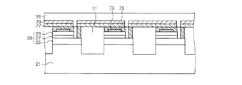
25 第1の導電型半導体層
27 活性層
29 第2の導電型半導体層
30 発光セル
71 絶縁層
73 反射層
75 保護金属層
Claims (14)
- 複数の非極性発光セルを有する発光ダイオードの製造方法であって、
上部表面がc面に対して一定の交差角をなす非極性または半極性の結晶面を有するGaN基板を用意し、
前記基板上に窒化物半導体層を成長させ、
前記窒化物半導体層をパターニングし、互いに分離された発光セルを形成し、前記発光セル間の分離領域の下方から前記基板を部分的に除去してリセス領域を形成し、
前記リセス領域を充填する絶縁層を形成し、
前記絶縁層を露出させるように、前記基板を少なくとも部分的に除去する発光ダイオードの製造方法であって、
前記窒化物半導体層は、第1の導電型半導体層、活性層、第2の導電型半導体層を有することを特徴とする発光ダイオードの製造方法。 - 前記基板を少なくとも部分的に除去した後、前記絶縁層間に露出した前記基板または前記窒化物半導体層の表面に粗面を形成することを特徴とする請求項1に記載の発光ダイオードの製造方法。
- 前記発光セルは、
それぞれ、第1の導電型半導体層と、
前記第1の導電型半導体層の一部領域上に配置される第2の導電型半導体層と、
前記第1の導電型半導体層と第2の導電型半導体層との間に介在された活性層と、を有することを特徴とする請求項1に記載の発光ダイオードの製造方法。 - 前記基板を除去する前に、前記発光セルを電気的に接続する配線を形成することを特徴とする請求項3に記載の発光ダイオードの製造方法。
- 前記配線を形成する前に、前記発光セル上に反射層を形成することを特徴とする請求項4に記載の発光ダイオードの製造方法。
- 前記GaN基板を除去する前に、
前記配線を覆う層間絶縁層を形成し、
前記層間絶縁層上に第2の基板をボンディングすることを特徴とする請求項4に記載の発光ダイオードの製造方法。 - 前記配線を形成する前に、前記発光セルの側面を覆う側面絶縁層を形成することを特徴とする請求項4に記載の発光ダイオードの製造方法。
- 前記リセス領域を充填する絶縁層は、前記発光セルを覆い、前記第1の導電型半導体層の他の領域及び前記第2の導電型半導体層の上部に開口部を有し、
前記基板を除去する前に、
前記絶縁層の開口部を通じて、隣り合う発光セルを電気的に接続するボンディングメタルを形成し、
前記ボンディングメタルに第2の基板をボンディングすることを特徴とする請求項3に記載の発光ダイオードの製造方法。 - 前記ボンディングメタルを形成する前に、前記第2の導電型半導体層上に反射層を形成することを特徴とする請求項8に記載の発光ダイオードの製造方法。
- 前記発光セルは、
それぞれ、第1の導電型半導体層と、
前記第1の導電型半導体層上に配置される第2の導電型半導体層と、
前記第1の導電型半導体層と第2の導電型半導体層との間に介在された活性層と、を有することを特徴とする請求項1に記載の発光ダイオードの製造方法。 - 前記基板を除去する前に、
前記発光セルの第1の導電型半導体層に電気的に接続された電極を形成し、前記電極は、それぞれ、前記リセス領域を充填する絶縁層上に延びたことを特徴とする請求項10に記載の発光ダイオードの製造方法。 - 前記電極を形成する際に、
前記第2の導電型半導体層上に反射層を形成し、
前記反射層を覆い、前記絶縁層上に延びる保護金属層を形成することを特徴とする請求項11に記載の発光ダイオードの製造方法。 - 前記基板を除去する前に、
前記電極を覆う層間絶縁層を形成し、
前記層間絶縁層に第2の基板をボンディングすることを特徴とする請求項11に記載の発光ダイオードの製造方法。 - 前記基板を除去した後、
前記リセス領域を充填する前記絶縁層をパターニングして、前記電極を露出させる開口部を形成し、
隣り合う発光セルを接続する配線を形成し、
前記配線は、それぞれ、その一端部が、前記絶縁層に形成された開口部を通じて、前記電極に電気的に接続されることを特徴とする請求項13に記載の発光ダイオードの製造方法。
Applications Claiming Priority (2)
| Application Number | Priority Date | Filing Date | Title |
|---|---|---|---|
| KR1020080138238A KR101533817B1 (ko) | 2008-12-31 | 2008-12-31 | 복수개의 비극성 발광셀들을 갖는 발광 소자 및 그것을 제조하는 방법 |
| KR10-2008-0138238 | 2008-12-31 |
Related Child Applications (1)
| Application Number | Title | Priority Date | Filing Date |
|---|---|---|---|
| JP2014096268A Division JP2014140084A (ja) | 2008-12-31 | 2014-05-07 | 複数の非極性発光セルを有する発光素子及びその製造方法 |
Publications (3)
| Publication Number | Publication Date |
|---|---|
| JP2010157692A JP2010157692A (ja) | 2010-07-15 |
| JP2010157692A5 JP2010157692A5 (ja) | 2012-12-06 |
| JP5641725B2 true JP5641725B2 (ja) | 2014-12-17 |
Family
ID=42283752
Family Applications (2)
| Application Number | Title | Priority Date | Filing Date |
|---|---|---|---|
| JP2009264005A Expired - Fee Related JP5641725B2 (ja) | 2008-12-31 | 2009-11-19 | 複数の非極性発光セルを有する発光素子及びその製造方法 |
| JP2014096268A Withdrawn JP2014140084A (ja) | 2008-12-31 | 2014-05-07 | 複数の非極性発光セルを有する発光素子及びその製造方法 |
Family Applications After (1)
| Application Number | Title | Priority Date | Filing Date |
|---|---|---|---|
| JP2014096268A Withdrawn JP2014140084A (ja) | 2008-12-31 | 2014-05-07 | 複数の非極性発光セルを有する発光素子及びその製造方法 |
Country Status (3)
| Country | Link |
|---|---|
| US (3) | US8211724B2 (ja) |
| JP (2) | JP5641725B2 (ja) |
| KR (1) | KR101533817B1 (ja) |
Families Citing this family (86)
| Publication number | Priority date | Publication date | Assignee | Title |
|---|---|---|---|---|
| US8698184B2 (en) * | 2011-01-21 | 2014-04-15 | Cree, Inc. | Light emitting diodes with low junction temperature and solid state backlight components including light emitting diodes with low junction temperature |
| US9443903B2 (en) | 2006-06-30 | 2016-09-13 | Cree, Inc. | Low temperature high strength metal stack for die attachment |
| US9461201B2 (en) | 2007-11-14 | 2016-10-04 | Cree, Inc. | Light emitting diode dielectric mirror |
| KR101017395B1 (ko) * | 2008-12-24 | 2011-02-28 | 서울옵토디바이스주식회사 | 복수개의 발광셀들을 갖는 발광 소자 및 그것을 제조하는 방법 |
| KR101557362B1 (ko) * | 2008-12-31 | 2015-10-08 | 서울바이오시스 주식회사 | 복수개의 비극성 발광셀들을 갖는 발광 소자 및 그것을 제조하는 방법 |
| KR101533817B1 (ko) | 2008-12-31 | 2015-07-09 | 서울바이오시스 주식회사 | 복수개의 비극성 발광셀들을 갖는 발광 소자 및 그것을 제조하는 방법 |
| US7923739B2 (en) * | 2009-06-05 | 2011-04-12 | Cree, Inc. | Solid state lighting device |
| US8598602B2 (en) | 2009-01-12 | 2013-12-03 | Cree, Inc. | Light emitting device packages with improved heat transfer |
| US9111778B2 (en) | 2009-06-05 | 2015-08-18 | Cree, Inc. | Light emitting diode (LED) devices, systems, and methods |
| US8860043B2 (en) | 2009-06-05 | 2014-10-14 | Cree, Inc. | Light emitting device packages, systems and methods |
| US8686445B1 (en) | 2009-06-05 | 2014-04-01 | Cree, Inc. | Solid state lighting devices and methods |
| US9583678B2 (en) | 2009-09-18 | 2017-02-28 | Soraa, Inc. | High-performance LED fabrication |
| US9435493B2 (en) | 2009-10-27 | 2016-09-06 | Cree, Inc. | Hybrid reflector system for lighting device |
| US8071401B2 (en) * | 2009-12-10 | 2011-12-06 | Walsin Lihwa Corporation | Method of forming vertical structure light emitting diode with heat exhaustion structure |
| US8648359B2 (en) * | 2010-06-28 | 2014-02-11 | Cree, Inc. | Light emitting devices and methods |
| US8269244B2 (en) | 2010-06-28 | 2012-09-18 | Cree, Inc. | LED package with efficient, isolated thermal path |
| USD643819S1 (en) | 2010-07-16 | 2011-08-23 | Cree, Inc. | Package for light emitting diode (LED) lighting |
| KR101138952B1 (ko) * | 2010-09-24 | 2012-04-25 | 서울옵토디바이스주식회사 | 복수개의 발광셀들을 갖는 웨이퍼 레벨 발광 다이오드 패키지 및 그것을 제조하는 방법 |
| US9070851B2 (en) | 2010-09-24 | 2015-06-30 | Seoul Semiconductor Co., Ltd. | Wafer-level light emitting diode package and method of fabricating the same |
| DE102010048159B4 (de) | 2010-10-11 | 2023-10-05 | OSRAM Opto Semiconductors Gesellschaft mit beschränkter Haftung | Leuchtdiodenchip |
| USD679842S1 (en) | 2011-01-03 | 2013-04-09 | Cree, Inc. | High brightness LED package |
| US11101408B2 (en) | 2011-02-07 | 2021-08-24 | Creeled, Inc. | Components and methods for light emitting diode (LED) lighting |
| US8610140B2 (en) | 2010-12-15 | 2013-12-17 | Cree, Inc. | Light emitting diode (LED) packages, systems, devices and related methods |
| US8536594B2 (en) * | 2011-01-28 | 2013-09-17 | Micron Technology, Inc. | Solid state lighting devices with reduced dimensions and methods of manufacturing |
| TW201251140A (en) | 2011-01-31 | 2012-12-16 | Cree Inc | High brightness light emitting diode (LED) packages, systems and methods with improved resin filling and high adhesion |
| DE102011013821A1 (de) | 2011-03-14 | 2012-09-20 | Osram Opto Semiconductors Gmbh | Verfahren zur Herstellung zumindest eines optoelektronischen Halbleiterchips |
| JP2012195435A (ja) * | 2011-03-16 | 2012-10-11 | Stanley Electric Co Ltd | 半導体発光素子の製造方法 |
| US8241932B1 (en) | 2011-03-17 | 2012-08-14 | Tsmc Solid State Lighting Ltd. | Methods of fabricating light emitting diode packages |
| US9236530B2 (en) | 2011-04-01 | 2016-01-12 | Soraa, Inc. | Miscut bulk substrates |
| US20120261686A1 (en) * | 2011-04-12 | 2012-10-18 | Lu Chi Wei | Light-emitting element and the manufacturing method thereof |
| US8592847B2 (en) * | 2011-04-15 | 2013-11-26 | Epistar Corporation | Light-emitting device |
| JP4989773B1 (ja) * | 2011-05-16 | 2012-08-01 | 株式会社東芝 | 半導体発光素子 |
| KR101799451B1 (ko) * | 2011-06-02 | 2017-11-20 | 엘지이노텍 주식회사 | 발광 소자 |
| US10243121B2 (en) | 2011-06-24 | 2019-03-26 | Cree, Inc. | High voltage monolithic LED chip with improved reliability |
| US9728676B2 (en) | 2011-06-24 | 2017-08-08 | Cree, Inc. | High voltage monolithic LED chip |
| CN103081136A (zh) | 2011-07-14 | 2013-05-01 | 松下电器产业株式会社 | 氮化物类半导体发光元件 |
| TW201310703A (zh) * | 2011-08-17 | 2013-03-01 | Ritedia Corp | 垂直式發光二極體結構及其製備方法 |
| KR20130021296A (ko) * | 2011-08-22 | 2013-03-05 | 엘지이노텍 주식회사 | 발광소자, 발광소자 패키지, 및 라이트 유닛 |
| US8686431B2 (en) | 2011-08-22 | 2014-04-01 | Soraa, Inc. | Gallium and nitrogen containing trilateral configuration for optical devices |
| US9646827B1 (en) * | 2011-08-23 | 2017-05-09 | Soraa, Inc. | Method for smoothing surface of a substrate containing gallium and nitrogen |
| KR101634369B1 (ko) * | 2011-12-27 | 2016-06-28 | 서울바이오시스 주식회사 | 복수개의 발광셀들을 갖는 웨이퍼 레벨 발광 다이오드 패키지 및 그것을 제조하는 방법 |
| KR102022659B1 (ko) * | 2012-02-20 | 2019-11-04 | 서울바이오시스 주식회사 | 고효율 발광 다이오드 및 그것을 제조하는 방법 |
| JP5992695B2 (ja) * | 2012-02-29 | 2016-09-14 | スタンレー電気株式会社 | 半導体発光素子アレイ及び車両用灯具 |
| FR2992465B1 (fr) * | 2012-06-22 | 2015-03-20 | Soitec Silicon On Insulator | Procede de fabrication collective de leds et structure pour la fabrication collective de leds |
| US11792898B2 (en) | 2012-07-01 | 2023-10-17 | Ideal Industries Lighting Llc | Enhanced fixtures for area lighting |
| US8816383B2 (en) * | 2012-07-06 | 2014-08-26 | Invensas Corporation | High performance light emitting diode with vias |
| CN103681723A (zh) * | 2012-08-30 | 2014-03-26 | 旭明光电股份有限公司 | 发光二极管 |
| DE102012109460B4 (de) | 2012-10-04 | 2024-03-07 | OSRAM Opto Semiconductors Gesellschaft mit beschränkter Haftung | Verfahren zur Herstellung eines Leuchtdioden-Displays und Leuchtdioden-Display |
| JP2014096455A (ja) * | 2012-11-08 | 2014-05-22 | Stanley Electric Co Ltd | 半導体発光素子アレイおよび車両用灯具 |
| US20140151630A1 (en) * | 2012-12-04 | 2014-06-05 | Feng-Hsu Fan | Protection for the epitaxial structure of metal devices |
| KR20140073351A (ko) | 2012-12-06 | 2014-06-16 | 엘지이노텍 주식회사 | 발광 소자 |
| TWI499091B (zh) * | 2012-12-18 | 2015-09-01 | Genesis Photonics Inc | 發光裝置 |
| TWI570955B (zh) | 2013-01-10 | 2017-02-11 | 晶元光電股份有限公司 | 發光元件 |
| KR101423717B1 (ko) * | 2013-02-08 | 2014-08-01 | 서울바이오시스 주식회사 | 복수개의 발광셀들을 갖는 발광 다이오드 패키지 및 그것을 제조하는 방법 |
| US9761774B2 (en) * | 2014-12-16 | 2017-09-12 | Epistar Corporation | Light-emitting element with protective cushioning |
| FR3011380B1 (fr) * | 2013-09-30 | 2017-01-13 | Aledia | Dispositif optoelectronique a diodes electroluminescentes |
| US10910350B2 (en) * | 2014-05-24 | 2021-02-02 | Hiphoton Co., Ltd. | Structure of a semiconductor array |
| DE102014116079A1 (de) * | 2014-11-04 | 2016-05-04 | Osram Opto Semiconductors Gmbh | Optoelektronisches Bauelement und Verfahren zu seiner Herstellung |
| CN105762245A (zh) * | 2014-12-18 | 2016-07-13 | 晶能光电(江西)有限公司 | 一种具有高出光效率的led芯片及其制备方法 |
| US10658546B2 (en) | 2015-01-21 | 2020-05-19 | Cree, Inc. | High efficiency LEDs and methods of manufacturing |
| DE102015105438A1 (de) * | 2015-04-09 | 2016-10-13 | M2K-Laser Gmbh | Monolithische Diodenlaseranordnung |
| TWI581460B (zh) | 2015-09-04 | 2017-05-01 | 錼創科技股份有限公司 | 發光元件及其製作方法 |
| JP6637703B2 (ja) * | 2015-09-10 | 2020-01-29 | アルパッド株式会社 | 半導体発光装置 |
| JP2017112203A (ja) * | 2015-12-16 | 2017-06-22 | シャープ株式会社 | 半導体発光素子 |
| KR102263041B1 (ko) | 2016-02-26 | 2021-06-09 | 삼성전자주식회사 | 멀티 컬러를 구현할 수 있는 발광 소자 |
| CN105702821B (zh) * | 2016-03-29 | 2018-01-30 | 苏州晶湛半导体有限公司 | 半导体发光器件及其制造方法 |
| CN205944139U (zh) | 2016-03-30 | 2017-02-08 | 首尔伟傲世有限公司 | 紫外线发光二极管封装件以及包含此的发光二极管模块 |
| US10529696B2 (en) * | 2016-04-12 | 2020-01-07 | Cree, Inc. | High density pixelated LED and devices and methods thereof |
| JP6645486B2 (ja) | 2017-02-13 | 2020-02-14 | 日亜化学工業株式会社 | 発光装置およびその製造方法 |
| US11177417B2 (en) * | 2017-02-13 | 2021-11-16 | Nichia Corporation | Light emitting device including phosphor layer with protrusions and recesses and method for manufacturing same |
| KR102385571B1 (ko) | 2017-03-31 | 2022-04-12 | 삼성전자주식회사 | 반도체 발광 소자 |
| JP6597837B2 (ja) * | 2017-06-30 | 2019-10-30 | 日亜化学工業株式会社 | 発光装置及びその製造方法 |
| KR102370621B1 (ko) * | 2017-08-24 | 2022-03-04 | 삼성전자주식회사 | 발광 패키지 및 이를 포함하는 발광 모듈 |
| KR101930006B1 (ko) * | 2017-09-26 | 2018-12-17 | 에피스타 코포레이션 | 발광소자 |
| US10797029B2 (en) | 2017-12-19 | 2020-10-06 | PlayNitride Inc. | Structure with micro device |
| US10804130B2 (en) | 2017-12-19 | 2020-10-13 | PlayNitride Inc. | Structure with micro device |
| CN109935668B (zh) | 2017-12-19 | 2021-08-24 | 英属开曼群岛商錼创科技股份有限公司 | 微型元件结构 |
| US10403799B1 (en) * | 2017-12-19 | 2019-09-03 | PlayNitride Inc. | Structure with micro device |
| US11469138B2 (en) * | 2018-05-04 | 2022-10-11 | Taiwan Semiconductor Manufacturing Company, Ltd. | Via for coupling attached component upper electrode to substrate |
| US11282984B2 (en) | 2018-10-05 | 2022-03-22 | Seoul Viosys Co., Ltd. | Light emitting device |
| US11967605B2 (en) * | 2018-11-13 | 2024-04-23 | Seoul Viosys Co., Ltd. | Light emitting device |
| TWI685096B (zh) * | 2018-11-21 | 2020-02-11 | 瑩耀科技股份有限公司 | 多層堆疊補隙發光半導體結構及其製作方法 |
| US10903265B2 (en) | 2018-12-21 | 2021-01-26 | Cree, Inc. | Pixelated-LED chips and chip array devices, and fabrication methods |
| CN111987083A (zh) * | 2019-05-23 | 2020-11-24 | 群创光电股份有限公司 | 电子装置以及发光单元 |
| WO2021087109A1 (en) | 2019-10-29 | 2021-05-06 | Cree, Inc. | Texturing for high density pixelated-led chips |
| KR102447407B1 (ko) * | 2020-11-12 | 2022-09-27 | 주식회사 에스엘바이오닉스 | 반도체 발광소자 |
Family Cites Families (37)
| Publication number | Priority date | Publication date | Assignee | Title |
|---|---|---|---|---|
| US20030189215A1 (en) * | 2002-04-09 | 2003-10-09 | Jong-Lam Lee | Method of fabricating vertical structure leds |
| JP3822545B2 (ja) | 2002-04-12 | 2006-09-20 | 士郎 酒井 | 発光装置 |
| US6828596B2 (en) * | 2002-06-13 | 2004-12-07 | Lumileds Lighting U.S., Llc | Contacting scheme for large and small area semiconductor light emitting flip chip devices |
| DE10228103A1 (de) | 2002-06-24 | 2004-01-15 | Bayer Cropscience Ag | Fungizide Wirkstoffkombinationen |
| EP2149907A3 (en) * | 2002-08-29 | 2014-05-07 | Seoul Semiconductor Co., Ltd. | Light-emitting device having light-emitting diodes |
| JP4572597B2 (ja) * | 2003-06-20 | 2010-11-04 | 日亜化学工業株式会社 | 窒化物半導体素子 |
| JP2007529105A (ja) * | 2003-07-16 | 2007-10-18 | 松下電器産業株式会社 | 半導体発光装置とその製造方法、照明装置および表示装置 |
| JP4449405B2 (ja) * | 2003-10-20 | 2010-04-14 | 日亜化学工業株式会社 | 窒化物半導体発光素子およびその製造方法 |
| US7723736B2 (en) * | 2004-12-14 | 2010-05-25 | Seoul Opto Device Co., Ltd. | Light emitting device having a plurality of light emitting cells and package mounting the same |
| JP4995722B2 (ja) * | 2004-12-22 | 2012-08-08 | パナソニック株式会社 | 半導体発光装置、照明モジュール、および照明装置 |
| US7378288B2 (en) * | 2005-01-11 | 2008-05-27 | Semileds Corporation | Systems and methods for producing light emitting diode array |
| TWI244228B (en) * | 2005-02-03 | 2005-11-21 | United Epitaxy Co Ltd | Light emitting device and manufacture method thereof |
| JP5008263B2 (ja) * | 2005-03-02 | 2012-08-22 | 日亜化学工業株式会社 | 半導体発光素子 |
| JP5059739B2 (ja) * | 2005-03-11 | 2012-10-31 | ソウル セミコンダクター カンパニー リミテッド | 直列接続された発光セルのアレイを有する発光ダイオードパッケージ |
| KR100599012B1 (ko) * | 2005-06-29 | 2006-07-12 | 서울옵토디바이스주식회사 | 열전도성 기판을 갖는 발광 다이오드 및 그것을 제조하는방법 |
| JP5058991B2 (ja) | 2005-06-29 | 2012-10-24 | コンプメディクス リミテッド | 導電ブリッジを備えるセンサ・アセンブリ |
| DE112006002927B4 (de) * | 2006-01-09 | 2010-06-02 | Seoul Opto Device Co. Ltd., Ansan | Licht emittierende Diode mit ITO-Schicht und Verfahren zur Herstellung einer solchen |
| KR101203138B1 (ko) * | 2006-01-12 | 2012-11-20 | 서울옵토디바이스주식회사 | 발광소자와 그 제조방법 |
| JP2007324581A (ja) * | 2006-05-01 | 2007-12-13 | Mitsubishi Chemicals Corp | 集積型半導体発光装置およびその製造方法 |
| JP5126875B2 (ja) * | 2006-08-11 | 2013-01-23 | シャープ株式会社 | 窒化物半導体発光素子の製造方法 |
| JP4915218B2 (ja) | 2006-11-17 | 2012-04-11 | ソニー株式会社 | 発光ダイオードの製造方法 |
| JP2008141015A (ja) | 2006-12-01 | 2008-06-19 | Mitsubishi Cable Ind Ltd | 発光ダイオード素子 |
| CN101652861B (zh) * | 2007-01-22 | 2013-01-23 | 科锐公司 | 容错发光体、包含容错发光体的系统以及制造容错发光体的方法 |
| US9024349B2 (en) * | 2007-01-22 | 2015-05-05 | Cree, Inc. | Wafer level phosphor coating method and devices fabricated utilizing method |
| JP2008186959A (ja) * | 2007-01-29 | 2008-08-14 | Toyoda Gosei Co Ltd | Iii−v族半導体素子、およびその製造方法 |
| KR100974923B1 (ko) * | 2007-03-19 | 2010-08-10 | 서울옵토디바이스주식회사 | 발광 다이오드 |
| DE102007019776A1 (de) | 2007-04-26 | 2008-10-30 | Osram Opto Semiconductors Gmbh | Optoelektronisches Bauelement und Verfahren zur Herstellung einer Mehrzahl optoelektronischer Bauelemente |
| KR100838197B1 (ko) | 2007-08-10 | 2008-06-16 | 서울옵토디바이스주식회사 | 개선된 전류분산 성능을 갖는 발광 다이오드 |
| KR100889956B1 (ko) * | 2007-09-27 | 2009-03-20 | 서울옵토디바이스주식회사 | 교류용 발광다이오드 |
| US8368100B2 (en) * | 2007-11-14 | 2013-02-05 | Cree, Inc. | Semiconductor light emitting diodes having reflective structures and methods of fabricating same |
| JP4981005B2 (ja) * | 2008-09-12 | 2012-07-18 | ローム株式会社 | 半導体発光装置 |
| JP5123269B2 (ja) * | 2008-09-30 | 2013-01-23 | ソウル オプト デバイス カンパニー リミテッド | 発光素子及びその製造方法 |
| KR101017394B1 (ko) | 2008-09-30 | 2011-02-28 | 서울옵토디바이스주식회사 | 발광 소자 및 그것을 제조하는 방법 |
| KR20100076083A (ko) * | 2008-12-17 | 2010-07-06 | 서울반도체 주식회사 | 복수개의 발광셀들을 갖는 발광 다이오드 및 그것을 제조하는 방법 |
| KR101557362B1 (ko) * | 2008-12-31 | 2015-10-08 | 서울바이오시스 주식회사 | 복수개의 비극성 발광셀들을 갖는 발광 소자 및 그것을 제조하는 방법 |
| KR101533817B1 (ko) | 2008-12-31 | 2015-07-09 | 서울바이오시스 주식회사 | 복수개의 비극성 발광셀들을 갖는 발광 소자 및 그것을 제조하는 방법 |
| JP2013510434A (ja) * | 2009-11-03 | 2013-03-21 | ザ リージェンツ オブ ザ ユニバーシティ オブ カリフォルニア | 低温水溶液中で多重表面上に酸化亜鉛層が被覆された高輝度発光ダイオード |
-
2008
- 2008-12-31 KR KR1020080138238A patent/KR101533817B1/ko active IP Right Grant
-
2009
- 2009-11-19 JP JP2009264005A patent/JP5641725B2/ja not_active Expired - Fee Related
- 2009-11-23 US US12/623,990 patent/US8211724B2/en active Active
-
2012
- 2012-05-29 US US13/482,851 patent/US8436389B2/en active Active
-
2013
- 2013-04-18 US US13/865,719 patent/US8648380B2/en not_active Expired - Fee Related
-
2014
- 2014-05-07 JP JP2014096268A patent/JP2014140084A/ja not_active Withdrawn
Also Published As
| Publication number | Publication date |
|---|---|
| JP2014140084A (ja) | 2014-07-31 |
| KR20100079693A (ko) | 2010-07-08 |
| JP2010157692A (ja) | 2010-07-15 |
| US20130228793A1 (en) | 2013-09-05 |
| US20120235158A1 (en) | 2012-09-20 |
| US8436389B2 (en) | 2013-05-07 |
| US20100163887A1 (en) | 2010-07-01 |
| KR101533817B1 (ko) | 2015-07-09 |
| US8648380B2 (en) | 2014-02-11 |
| US8211724B2 (en) | 2012-07-03 |
Similar Documents
| Publication | Publication Date | Title |
|---|---|---|
| JP5641725B2 (ja) | 複数の非極性発光セルを有する発光素子及びその製造方法 | |
| JP5016018B2 (ja) | 複数の非極性発光セルを有する発光素子及びその製造方法 | |
| US9337175B2 (en) | Light emitting device and method of fabricating the same | |
| JP6087409B2 (ja) | 発光素子 | |
| US8937327B2 (en) | Light emitting device having plurality of light emitting cells and method of fabricating the same | |
| JP5624747B2 (ja) | 複数の発光セルを有する発光素子及びその製造方法 | |
| KR20100108906A (ko) | 복수개의 발광셀들을 갖는 발광 소자 및 그것을 제조하는 방법 | |
| KR20100075420A (ko) | 복수개의 발광셀들을 갖는 발광 소자 및 그것을 제조하는 방법 | |
| KR101599529B1 (ko) | 복수개의 비극성 발광셀들을 갖는 발광 소자 및 그것을 제조하는 방법 | |
| KR101457203B1 (ko) | 복수개의 반도체 적층 구조를 갖는 발광 다이오드 | |
| KR101564343B1 (ko) | 복수개의 비극성 발광셀들을 갖는 발광 소자 및 그것을 제조하는 방법 | |
| KR101564344B1 (ko) | 복수개의 비극성 발광셀들을 갖는 발광 소자 및 그것을 제조하는 방법 | |
| KR20130030279A (ko) | 서로 이격된 반도체층들을 갖는 발광 소자 및 그것을 제조하는 방법 |
Legal Events
| Date | Code | Title | Description |
|---|---|---|---|
| A521 | Request for written amendment filed |
Free format text: JAPANESE INTERMEDIATE CODE: A523 Effective date: 20121018 |
|
| A621 | Written request for application examination |
Free format text: JAPANESE INTERMEDIATE CODE: A621 Effective date: 20121018 |
|
| A977 | Report on retrieval |
Free format text: JAPANESE INTERMEDIATE CODE: A971007 Effective date: 20130918 |
|
| A131 | Notification of reasons for refusal |
Free format text: JAPANESE INTERMEDIATE CODE: A131 Effective date: 20130924 |
|
| A521 | Request for written amendment filed |
Free format text: JAPANESE INTERMEDIATE CODE: A523 Effective date: 20131224 |
|
| A131 | Notification of reasons for refusal |
Free format text: JAPANESE INTERMEDIATE CODE: A131 Effective date: 20140204 |
|
| A521 | Request for written amendment filed |
Free format text: JAPANESE INTERMEDIATE CODE: A523 Effective date: 20140507 |
|
| TRDD | Decision of grant or rejection written | ||
| A01 | Written decision to grant a patent or to grant a registration (utility model) |
Free format text: JAPANESE INTERMEDIATE CODE: A01 Effective date: 20141014 |
|
| A61 | First payment of annual fees (during grant procedure) |
Free format text: JAPANESE INTERMEDIATE CODE: A61 Effective date: 20141028 |
|
| R150 | Certificate of patent or registration of utility model |
Ref document number: 5641725 Country of ref document: JP Free format text: JAPANESE INTERMEDIATE CODE: R150 |
|
| R250 | Receipt of annual fees |
Free format text: JAPANESE INTERMEDIATE CODE: R250 |
|
| R250 | Receipt of annual fees |
Free format text: JAPANESE INTERMEDIATE CODE: R250 |
|
| R250 | Receipt of annual fees |
Free format text: JAPANESE INTERMEDIATE CODE: R250 |
|
| R250 | Receipt of annual fees |
Free format text: JAPANESE INTERMEDIATE CODE: R250 |
|
| R250 | Receipt of annual fees |
Free format text: JAPANESE INTERMEDIATE CODE: R250 |
|
| LAPS | Cancellation because of no payment of annual fees |