JP5610759B2 - Soi基板の作製方法、半導体装置の作製方法 - Google Patents
Soi基板の作製方法、半導体装置の作製方法 Download PDFInfo
- Publication number
- JP5610759B2 JP5610759B2 JP2009280207A JP2009280207A JP5610759B2 JP 5610759 B2 JP5610759 B2 JP 5610759B2 JP 2009280207 A JP2009280207 A JP 2009280207A JP 2009280207 A JP2009280207 A JP 2009280207A JP 5610759 B2 JP5610759 B2 JP 5610759B2
- Authority
- JP
- Japan
- Prior art keywords
- substrate
- single crystal
- semiconductor layer
- crystal semiconductor
- oxygen
- Prior art date
- Legal status (The legal status is an assumption and is not a legal conclusion. Google has not performed a legal analysis and makes no representation as to the accuracy of the status listed.)
- Expired - Fee Related
Links
- 239000004065 semiconductor Substances 0.000 title claims description 246
- 239000000758 substrate Substances 0.000 title claims description 229
- 238000000034 method Methods 0.000 title claims description 78
- 238000004519 manufacturing process Methods 0.000 title claims description 37
- QVGXLLKOCUKJST-UHFFFAOYSA-N atomic oxygen Chemical compound [O] QVGXLLKOCUKJST-UHFFFAOYSA-N 0.000 claims description 137
- 239000001301 oxygen Substances 0.000 claims description 137
- 229910052760 oxygen Inorganic materials 0.000 claims description 137
- 239000013078 crystal Substances 0.000 claims description 130
- 239000012298 atmosphere Substances 0.000 claims description 75
- 238000002844 melting Methods 0.000 claims description 19
- 230000008018 melting Effects 0.000 claims description 19
- KRHYYFGTRYWZRS-UHFFFAOYSA-N Fluorane Chemical compound F KRHYYFGTRYWZRS-UHFFFAOYSA-N 0.000 claims description 15
- 239000007789 gas Substances 0.000 claims description 15
- 229910000040 hydrogen fluoride Inorganic materials 0.000 claims description 15
- 230000001603 reducing effect Effects 0.000 claims description 15
- 230000001678 irradiating effect Effects 0.000 claims description 8
- 239000010408 film Substances 0.000 description 236
- 239000010410 layer Substances 0.000 description 217
- XUIMIQQOPSSXEZ-UHFFFAOYSA-N Silicon Chemical compound [Si] XUIMIQQOPSSXEZ-UHFFFAOYSA-N 0.000 description 51
- 229910052710 silicon Inorganic materials 0.000 description 51
- 239000010703 silicon Substances 0.000 description 51
- 238000010438 heat treatment Methods 0.000 description 48
- 238000009792 diffusion process Methods 0.000 description 46
- 239000012535 impurity Substances 0.000 description 43
- 239000000523 sample Substances 0.000 description 36
- 239000011229 interlayer Substances 0.000 description 32
- 150000002500 ions Chemical class 0.000 description 30
- 239000001257 hydrogen Substances 0.000 description 26
- 229910052739 hydrogen Inorganic materials 0.000 description 26
- VYPSYNLAJGMNEJ-UHFFFAOYSA-N Silicium dioxide Chemical compound O=[Si]=O VYPSYNLAJGMNEJ-UHFFFAOYSA-N 0.000 description 22
- 150000002431 hydrogen Chemical class 0.000 description 20
- 229910052581 Si3N4 Inorganic materials 0.000 description 19
- 238000000926 separation method Methods 0.000 description 19
- HQVNEWCFYHHQES-UHFFFAOYSA-N silicon nitride Chemical compound N12[Si]34N5[Si]62N3[Si]51N64 HQVNEWCFYHHQES-UHFFFAOYSA-N 0.000 description 19
- 229910052734 helium Inorganic materials 0.000 description 18
- 239000001307 helium Substances 0.000 description 18
- SWQJXJOGLNCZEY-UHFFFAOYSA-N helium atom Chemical compound [He] SWQJXJOGLNCZEY-UHFFFAOYSA-N 0.000 description 18
- 230000015572 biosynthetic process Effects 0.000 description 16
- 229910052814 silicon oxide Inorganic materials 0.000 description 16
- IJGRMHOSHXDMSA-UHFFFAOYSA-N Atomic nitrogen Chemical compound N#N IJGRMHOSHXDMSA-UHFFFAOYSA-N 0.000 description 14
- 239000000463 material Substances 0.000 description 13
- 229910052751 metal Inorganic materials 0.000 description 12
- 239000002184 metal Substances 0.000 description 12
- 229910021332 silicide Inorganic materials 0.000 description 12
- FVBUAEGBCNSCDD-UHFFFAOYSA-N silicide(4-) Chemical group [Si-4] FVBUAEGBCNSCDD-UHFFFAOYSA-N 0.000 description 12
- 230000000694 effects Effects 0.000 description 11
- 238000005530 etching Methods 0.000 description 11
- 238000005259 measurement Methods 0.000 description 10
- 238000004458 analytical method Methods 0.000 description 9
- 239000004020 conductor Substances 0.000 description 9
- 230000006698 induction Effects 0.000 description 9
- 239000007787 solid Substances 0.000 description 9
- 238000001556 precipitation Methods 0.000 description 8
- 230000001737 promoting effect Effects 0.000 description 8
- 239000013074 reference sample Substances 0.000 description 8
- UFHFLCQGNIYNRP-UHFFFAOYSA-N Hydrogen Chemical compound [H][H] UFHFLCQGNIYNRP-UHFFFAOYSA-N 0.000 description 7
- 229910052782 aluminium Inorganic materials 0.000 description 7
- XAGFODPZIPBFFR-UHFFFAOYSA-N aluminium Chemical compound [Al] XAGFODPZIPBFFR-UHFFFAOYSA-N 0.000 description 7
- 229910052785 arsenic Inorganic materials 0.000 description 7
- RQNWIZPPADIBDY-UHFFFAOYSA-N arsenic atom Chemical compound [As] RQNWIZPPADIBDY-UHFFFAOYSA-N 0.000 description 7
- 229910052757 nitrogen Inorganic materials 0.000 description 7
- 239000002356 single layer Substances 0.000 description 7
- 230000003746 surface roughness Effects 0.000 description 7
- OAICVXFJPJFONN-UHFFFAOYSA-N Phosphorus Chemical compound [P] OAICVXFJPJFONN-UHFFFAOYSA-N 0.000 description 6
- 238000001994 activation Methods 0.000 description 6
- 239000011521 glass Substances 0.000 description 6
- 229910052698 phosphorus Inorganic materials 0.000 description 6
- 239000011574 phosphorus Substances 0.000 description 6
- 230000008569 process Effects 0.000 description 6
- 239000010453 quartz Substances 0.000 description 6
- 238000001816 cooling Methods 0.000 description 5
- 230000007423 decrease Effects 0.000 description 5
- 229910052736 halogen Inorganic materials 0.000 description 5
- XMBWDFGMSWQBCA-UHFFFAOYSA-N hydrogen iodide Chemical compound I XMBWDFGMSWQBCA-UHFFFAOYSA-N 0.000 description 5
- 229910000043 hydrogen iodide Inorganic materials 0.000 description 5
- 238000005468 ion implantation Methods 0.000 description 5
- 230000003647 oxidation Effects 0.000 description 5
- 238000007254 oxidation reaction Methods 0.000 description 5
- 238000006722 reduction reaction Methods 0.000 description 5
- 238000004381 surface treatment Methods 0.000 description 5
- 229910052721 tungsten Inorganic materials 0.000 description 5
- 239000010937 tungsten Substances 0.000 description 5
- ZOXJGFHDIHLPTG-UHFFFAOYSA-N Boron Chemical compound [B] ZOXJGFHDIHLPTG-UHFFFAOYSA-N 0.000 description 4
- 229910052796 boron Inorganic materials 0.000 description 4
- 150000002367 halogens Chemical class 0.000 description 4
- 239000011261 inert gas Substances 0.000 description 4
- 238000009832 plasma treatment Methods 0.000 description 4
- 239000000243 solution Substances 0.000 description 4
- WFKWXMTUELFFGS-UHFFFAOYSA-N tungsten Chemical compound [W] WFKWXMTUELFFGS-UHFFFAOYSA-N 0.000 description 4
- ZOKXTWBITQBERF-UHFFFAOYSA-N Molybdenum Chemical compound [Mo] ZOKXTWBITQBERF-UHFFFAOYSA-N 0.000 description 3
- RTAQQCXQSZGOHL-UHFFFAOYSA-N Titanium Chemical compound [Ti] RTAQQCXQSZGOHL-UHFFFAOYSA-N 0.000 description 3
- 230000001133 acceleration Effects 0.000 description 3
- 230000004913 activation Effects 0.000 description 3
- 238000011109 contamination Methods 0.000 description 3
- 238000009413 insulation Methods 0.000 description 3
- 229910052750 molybdenum Inorganic materials 0.000 description 3
- 239000011733 molybdenum Substances 0.000 description 3
- 230000001681 protective effect Effects 0.000 description 3
- 230000009467 reduction Effects 0.000 description 3
- 238000001004 secondary ion mass spectrometry Methods 0.000 description 3
- 229910052719 titanium Inorganic materials 0.000 description 3
- 239000010936 titanium Substances 0.000 description 3
- QGZKDVFQNNGYKY-UHFFFAOYSA-N Ammonia Chemical compound N QGZKDVFQNNGYKY-UHFFFAOYSA-N 0.000 description 2
- XKRFYHLGVUSROY-UHFFFAOYSA-N Argon Chemical compound [Ar] XKRFYHLGVUSROY-UHFFFAOYSA-N 0.000 description 2
- OKTJSMMVPCPJKN-UHFFFAOYSA-N Carbon Chemical compound [C] OKTJSMMVPCPJKN-UHFFFAOYSA-N 0.000 description 2
- UGFAIRIUMAVXCW-UHFFFAOYSA-N Carbon monoxide Chemical compound [O+]#[C-] UGFAIRIUMAVXCW-UHFFFAOYSA-N 0.000 description 2
- RYGMFSIKBFXOCR-UHFFFAOYSA-N Copper Chemical compound [Cu] RYGMFSIKBFXOCR-UHFFFAOYSA-N 0.000 description 2
- VEXZGXHMUGYJMC-UHFFFAOYSA-N Hydrochloric acid Chemical compound Cl VEXZGXHMUGYJMC-UHFFFAOYSA-N 0.000 description 2
- XEEYBQQBJWHFJM-UHFFFAOYSA-N Iron Chemical compound [Fe] XEEYBQQBJWHFJM-UHFFFAOYSA-N 0.000 description 2
- PXHVJJICTQNCMI-UHFFFAOYSA-N Nickel Chemical compound [Ni] PXHVJJICTQNCMI-UHFFFAOYSA-N 0.000 description 2
- 239000004642 Polyimide Substances 0.000 description 2
- BQCADISMDOOEFD-UHFFFAOYSA-N Silver Chemical compound [Ag] BQCADISMDOOEFD-UHFFFAOYSA-N 0.000 description 2
- BOTDANWDWHJENH-UHFFFAOYSA-N Tetraethyl orthosilicate Chemical compound CCO[Si](OCC)(OCC)OCC BOTDANWDWHJENH-UHFFFAOYSA-N 0.000 description 2
- NIXOWILDQLNWCW-UHFFFAOYSA-N acrylic acid group Chemical group C(C=C)(=O)O NIXOWILDQLNWCW-UHFFFAOYSA-N 0.000 description 2
- 125000004429 atom Chemical group 0.000 description 2
- 230000008901 benefit Effects 0.000 description 2
- 229910052799 carbon Inorganic materials 0.000 description 2
- 229910002091 carbon monoxide Inorganic materials 0.000 description 2
- 238000005229 chemical vapour deposition Methods 0.000 description 2
- 229910052802 copper Inorganic materials 0.000 description 2
- 239000010949 copper Substances 0.000 description 2
- PMHQVHHXPFUNSP-UHFFFAOYSA-M copper(1+);methylsulfanylmethane;bromide Chemical compound Br[Cu].CSC PMHQVHHXPFUNSP-UHFFFAOYSA-M 0.000 description 2
- 230000002542 deteriorative effect Effects 0.000 description 2
- KPUWHANPEXNPJT-UHFFFAOYSA-N disiloxane Chemical class [SiH3]O[SiH3] KPUWHANPEXNPJT-UHFFFAOYSA-N 0.000 description 2
- 238000000635 electron micrograph Methods 0.000 description 2
- 229910052732 germanium Inorganic materials 0.000 description 2
- GNPVGFCGXDBREM-UHFFFAOYSA-N germanium atom Chemical compound [Ge] GNPVGFCGXDBREM-UHFFFAOYSA-N 0.000 description 2
- 238000005247 gettering Methods 0.000 description 2
- PCHJSUWPFVWCPO-UHFFFAOYSA-N gold Chemical compound [Au] PCHJSUWPFVWCPO-UHFFFAOYSA-N 0.000 description 2
- 229910052737 gold Inorganic materials 0.000 description 2
- 239000010931 gold Substances 0.000 description 2
- 150000002363 hafnium compounds Chemical class 0.000 description 2
- 229910000041 hydrogen chloride Inorganic materials 0.000 description 2
- IXCSERBJSXMMFS-UHFFFAOYSA-N hydrogen chloride Substances Cl.Cl IXCSERBJSXMMFS-UHFFFAOYSA-N 0.000 description 2
- -1 hydrogen ions Chemical class 0.000 description 2
- AMGQUBHHOARCQH-UHFFFAOYSA-N indium;oxotin Chemical compound [In].[Sn]=O AMGQUBHHOARCQH-UHFFFAOYSA-N 0.000 description 2
- 238000010884 ion-beam technique Methods 0.000 description 2
- 238000002955 isolation Methods 0.000 description 2
- 239000012788 optical film Substances 0.000 description 2
- 150000001282 organosilanes Chemical class 0.000 description 2
- 230000001590 oxidative effect Effects 0.000 description 2
- TWNQGVIAIRXVLR-UHFFFAOYSA-N oxo(oxoalumanyloxy)alumane Chemical compound O=[Al]O[Al]=O TWNQGVIAIRXVLR-UHFFFAOYSA-N 0.000 description 2
- 229920001721 polyimide Polymers 0.000 description 2
- 229920000642 polymer Polymers 0.000 description 2
- 229910052709 silver Inorganic materials 0.000 description 2
- 239000004332 silver Substances 0.000 description 2
- 238000004544 sputter deposition Methods 0.000 description 2
- 229910001220 stainless steel Inorganic materials 0.000 description 2
- 239000010935 stainless steel Substances 0.000 description 2
- 239000000126 substance Substances 0.000 description 2
- 238000011282 treatment Methods 0.000 description 2
- ZCYVEMRRCGMTRW-UHFFFAOYSA-N 7553-56-2 Chemical compound [I] ZCYVEMRRCGMTRW-UHFFFAOYSA-N 0.000 description 1
- VHUUQVKOLVNVRT-UHFFFAOYSA-N Ammonium hydroxide Chemical compound [NH4+].[OH-] VHUUQVKOLVNVRT-UHFFFAOYSA-N 0.000 description 1
- MHAJPDPJQMAIIY-UHFFFAOYSA-N Hydrogen peroxide Chemical compound OO MHAJPDPJQMAIIY-UHFFFAOYSA-N 0.000 description 1
- DGAQECJNVWCQMB-PUAWFVPOSA-M Ilexoside XXIX Chemical compound C[C@@H]1CC[C@@]2(CC[C@@]3(C(=CC[C@H]4[C@]3(CC[C@@H]5[C@@]4(CC[C@@H](C5(C)C)OS(=O)(=O)[O-])C)C)[C@@H]2[C@]1(C)O)C)C(=O)O[C@H]6[C@@H]([C@H]([C@@H]([C@H](O6)CO)O)O)O.[Na+] DGAQECJNVWCQMB-PUAWFVPOSA-M 0.000 description 1
- CBENFWSGALASAD-UHFFFAOYSA-N Ozone Chemical compound [O-][O+]=O CBENFWSGALASAD-UHFFFAOYSA-N 0.000 description 1
- 230000009471 action Effects 0.000 description 1
- 229910021529 ammonia Inorganic materials 0.000 description 1
- 235000011114 ammonium hydroxide Nutrition 0.000 description 1
- 229910052786 argon Inorganic materials 0.000 description 1
- 239000000919 ceramic Substances 0.000 description 1
- 230000008859 change Effects 0.000 description 1
- 239000007795 chemical reaction product Substances 0.000 description 1
- 238000004140 cleaning Methods 0.000 description 1
- 229910017052 cobalt Inorganic materials 0.000 description 1
- 239000010941 cobalt Substances 0.000 description 1
- GUTLYIVDDKVIGB-UHFFFAOYSA-N cobalt atom Chemical compound [Co] GUTLYIVDDKVIGB-UHFFFAOYSA-N 0.000 description 1
- 230000003247 decreasing effect Effects 0.000 description 1
- 230000007547 defect Effects 0.000 description 1
- 238000001312 dry etching Methods 0.000 description 1
- 238000002474 experimental method Methods 0.000 description 1
- 150000004820 halides Chemical class 0.000 description 1
- 229910001385 heavy metal Inorganic materials 0.000 description 1
- 239000012212 insulator Substances 0.000 description 1
- 239000011630 iodine Substances 0.000 description 1
- 229910052740 iodine Inorganic materials 0.000 description 1
- 229910052742 iron Inorganic materials 0.000 description 1
- 150000002739 metals Chemical class 0.000 description 1
- 239000011259 mixed solution Substances 0.000 description 1
- 238000002156 mixing Methods 0.000 description 1
- 229910021421 monocrystalline silicon Inorganic materials 0.000 description 1
- 229910052759 nickel Inorganic materials 0.000 description 1
- 150000004767 nitrides Chemical class 0.000 description 1
- 239000012299 nitrogen atmosphere Substances 0.000 description 1
- 238000005498 polishing Methods 0.000 description 1
- 238000007517 polishing process Methods 0.000 description 1
- 238000002360 preparation method Methods 0.000 description 1
- 239000000047 product Substances 0.000 description 1
- 239000002994 raw material Substances 0.000 description 1
- 238000005464 sample preparation method Methods 0.000 description 1
- 229910052594 sapphire Inorganic materials 0.000 description 1
- 239000010980 sapphire Substances 0.000 description 1
- 238000004335 scaling law Methods 0.000 description 1
- 229910052708 sodium Inorganic materials 0.000 description 1
- 239000011734 sodium Substances 0.000 description 1
- 239000007790 solid phase Substances 0.000 description 1
- 238000005728 strengthening Methods 0.000 description 1
- XLYOFNOQVPJJNP-UHFFFAOYSA-N water Substances O XLYOFNOQVPJJNP-UHFFFAOYSA-N 0.000 description 1
Images


Classifications
-
- H—ELECTRICITY
- H01—ELECTRIC ELEMENTS
- H01L—SEMICONDUCTOR DEVICES NOT COVERED BY CLASS H10
- H01L21/00—Processes or apparatus adapted for the manufacture or treatment of semiconductor or solid state devices or of parts thereof
- H01L21/70—Manufacture or treatment of devices consisting of a plurality of solid state components formed in or on a common substrate or of parts thereof; Manufacture of integrated circuit devices or of parts thereof
- H01L21/71—Manufacture of specific parts of devices defined in group H01L21/70
- H01L21/76—Making of isolation regions between components
- H01L21/762—Dielectric regions, e.g. EPIC dielectric isolation, LOCOS; Trench refilling techniques, SOI technology, use of channel stoppers
- H01L21/7624—Dielectric regions, e.g. EPIC dielectric isolation, LOCOS; Trench refilling techniques, SOI technology, use of channel stoppers using semiconductor on insulator [SOI] technology
- H01L21/76251—Dielectric regions, e.g. EPIC dielectric isolation, LOCOS; Trench refilling techniques, SOI technology, use of channel stoppers using semiconductor on insulator [SOI] technology using bonding techniques
- H01L21/76254—Dielectric regions, e.g. EPIC dielectric isolation, LOCOS; Trench refilling techniques, SOI technology, use of channel stoppers using semiconductor on insulator [SOI] technology using bonding techniques with separation/delamination along an ion implanted layer, e.g. Smart-cut, Unibond
-
- H—ELECTRICITY
- H01—ELECTRIC ELEMENTS
- H01L—SEMICONDUCTOR DEVICES NOT COVERED BY CLASS H10
- H01L21/00—Processes or apparatus adapted for the manufacture or treatment of semiconductor or solid state devices or of parts thereof
- H01L21/70—Manufacture or treatment of devices consisting of a plurality of solid state components formed in or on a common substrate or of parts thereof; Manufacture of integrated circuit devices or of parts thereof
- H01L21/71—Manufacture of specific parts of devices defined in group H01L21/70
- H01L21/76—Making of isolation regions between components
- H01L21/762—Dielectric regions, e.g. EPIC dielectric isolation, LOCOS; Trench refilling techniques, SOI technology, use of channel stoppers
- H01L21/7624—Dielectric regions, e.g. EPIC dielectric isolation, LOCOS; Trench refilling techniques, SOI technology, use of channel stoppers using semiconductor on insulator [SOI] technology
-
- H—ELECTRICITY
- H01—ELECTRIC ELEMENTS
- H01L—SEMICONDUCTOR DEVICES NOT COVERED BY CLASS H10
- H01L21/00—Processes or apparatus adapted for the manufacture or treatment of semiconductor or solid state devices or of parts thereof
- H01L21/02—Manufacture or treatment of semiconductor devices or of parts thereof
- H01L21/02104—Forming layers
- H01L21/02365—Forming inorganic semiconducting materials on a substrate
- H01L21/02518—Deposited layers
- H01L21/02587—Structure
- H01L21/0259—Microstructure
- H01L21/02598—Microstructure monocrystalline
-
- H—ELECTRICITY
- H01—ELECTRIC ELEMENTS
- H01L—SEMICONDUCTOR DEVICES NOT COVERED BY CLASS H10
- H01L21/00—Processes or apparatus adapted for the manufacture or treatment of semiconductor or solid state devices or of parts thereof
- H01L21/02—Manufacture or treatment of semiconductor devices or of parts thereof
- H01L21/04—Manufacture or treatment of semiconductor devices or of parts thereof the devices having potential barriers, e.g. a PN junction, depletion layer or carrier concentration layer
- H01L21/18—Manufacture or treatment of semiconductor devices or of parts thereof the devices having potential barriers, e.g. a PN junction, depletion layer or carrier concentration layer the devices having semiconductor bodies comprising elements of Group IV of the Periodic Table or AIIIBV compounds with or without impurities, e.g. doping materials
- H01L21/26—Bombardment with radiation
- H01L21/263—Bombardment with radiation with high-energy radiation
- H01L21/265—Bombardment with radiation with high-energy radiation producing ion implantation
-
- H—ELECTRICITY
- H01—ELECTRIC ELEMENTS
- H01L—SEMICONDUCTOR DEVICES NOT COVERED BY CLASS H10
- H01L21/00—Processes or apparatus adapted for the manufacture or treatment of semiconductor or solid state devices or of parts thereof
- H01L21/02—Manufacture or treatment of semiconductor devices or of parts thereof
- H01L21/04—Manufacture or treatment of semiconductor devices or of parts thereof the devices having potential barriers, e.g. a PN junction, depletion layer or carrier concentration layer
- H01L21/18—Manufacture or treatment of semiconductor devices or of parts thereof the devices having potential barriers, e.g. a PN junction, depletion layer or carrier concentration layer the devices having semiconductor bodies comprising elements of Group IV of the Periodic Table or AIIIBV compounds with or without impurities, e.g. doping materials
- H01L21/26—Bombardment with radiation
- H01L21/263—Bombardment with radiation with high-energy radiation
- H01L21/268—Bombardment with radiation with high-energy radiation using electromagnetic radiation, e.g. laser radiation
-
- H—ELECTRICITY
- H01—ELECTRIC ELEMENTS
- H01L—SEMICONDUCTOR DEVICES NOT COVERED BY CLASS H10
- H01L21/00—Processes or apparatus adapted for the manufacture or treatment of semiconductor or solid state devices or of parts thereof
- H01L21/02—Manufacture or treatment of semiconductor devices or of parts thereof
- H01L21/04—Manufacture or treatment of semiconductor devices or of parts thereof the devices having potential barriers, e.g. a PN junction, depletion layer or carrier concentration layer
- H01L21/18—Manufacture or treatment of semiconductor devices or of parts thereof the devices having potential barriers, e.g. a PN junction, depletion layer or carrier concentration layer the devices having semiconductor bodies comprising elements of Group IV of the Periodic Table or AIIIBV compounds with or without impurities, e.g. doping materials
- H01L21/30—Treatment of semiconductor bodies using processes or apparatus not provided for in groups H01L21/20 - H01L21/26
- H01L21/324—Thermal treatment for modifying the properties of semiconductor bodies, e.g. annealing, sintering
Landscapes
- Engineering & Computer Science (AREA)
- Physics & Mathematics (AREA)
- Power Engineering (AREA)
- Microelectronics & Electronic Packaging (AREA)
- Condensed Matter Physics & Semiconductors (AREA)
- General Physics & Mathematics (AREA)
- Manufacturing & Machinery (AREA)
- Computer Hardware Design (AREA)
- High Energy & Nuclear Physics (AREA)
- Health & Medical Sciences (AREA)
- Toxicology (AREA)
- Optics & Photonics (AREA)
- Electromagnetism (AREA)
- Chemical & Material Sciences (AREA)
- Crystallography & Structural Chemistry (AREA)
- Recrystallisation Techniques (AREA)
- Thin Film Transistor (AREA)
- Pressure Welding/Diffusion-Bonding (AREA)
Description
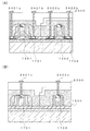
本実施の形態では、SOI基板の作製方法の一例について説明する。
本実施の形態では、SOI基板を用いて形成した半導体装置の作製方法の一例について説明する。
本実施の形態では、SOI基板を用いて形成した半導体装置の作製方法の一例について説明する。
SOI基板の作製方法の一例ついて説明する。
まず、塩化水素を含む雰囲気中で950℃の温度で熱酸化を行うことによって、シリコンウェハの表面に熱酸化膜を100nmの膜厚で形成した。
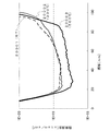
リファレンスサンプルは、レーザー光の照射を行っていないサンプルである。
リファレンスサンプル(レーザー未照射)、第1のサンプル(レーザー照射(室温))、第2のサンプル(レーザー照射(300℃))、及び第3のサンプル(レーザー照射(500℃))の単結晶半導体層中の酸素濃度を測定するため、SIMS分析(2次イオン質量分析)を行った。
まず、図16〜図18のグラフの見方について説明する。
サンプル作製に使用したシリコンウェハは、酸素濃度が1.0×10¹⁸〜2.0×10¹⁸atom/cm3になるように制御されたシリコンウェハであった。
11a 第1の領域
11b 第2の領域
11c 脆化領域
11d 溶融状態の半導体
12 接合層
13 ベース基板
14 レーザー光
80 破線
81 破線
82 破線
83 破線
90 破線
100 ベース基板
200 接合層
300 単結晶半導体層
301 島状半導体層
301a 不純物領域
301b 不純物領域
302 島状半導体層
302a 不純物領域
302b 不純物領域
400 ゲート絶縁膜
501 ゲート電極
502 ゲート電極
600 層間絶縁膜
701a 配線
701b 配線
701b 配線
701c 配線
701c 配線
702a 配線
1100 ベース基板
1200 接合層
1300 単結晶半導体層
1301 島状半導体層
1302 島状半導体層
1311a 低濃度不純物領域
1311b 低濃度不純物領域
1312a 低濃度不純物領域
1312b 低濃度不純物領域
1321a 高濃度不純物領域
1321b 高濃度不純物領域
1322a 高濃度不純物領域
1322b 高濃度不純物領域
1400 マスク絶縁膜
1500 埋込絶縁膜
1601 ゲート絶縁膜
1602 ゲート絶縁膜
1701 ゲート電極
1702 ゲート電極
1801 酸化膜
1802 酸化膜
1901 サイドウォール形成用絶縁膜
1901a サイドウォール
1901b サイドウォール
1902 サイドウォール形成用絶縁膜
1902a サイドウォール
1902b サイドウォール
1903 サイドウォール形成用絶縁膜
1903a サイドウォール
1903b サイドウォール
2000 金属膜
2001a シリサイド領域
2001b シリサイド領域
2001c シリサイド領域
2002a シリサイド領域
2002b シリサイド領域
2002c シリサイド領域
2100 層間絶縁膜
2101 層間絶縁膜
2101a サイドウォール
2101b サイドウォール
2200 層間絶縁膜
2300 層間絶縁膜
2401a 配線
2401b 配線
2401c 配線
2402a 配線
2402b 配線
2402c 配線
5100a 半導体基板
5100b 半導体基板
5100c 半導体基板
5102a 接合層
5102b 接合層
5102c 接合層
5104a 脆化領域
5104b 脆化領域
5104c 脆化領域
5120 ベース基板
5124a 単結晶半導体膜
5124b 単結晶半導体膜
5124c 単結晶半導体膜
8001 破線
8002 破線
8011a 破線
8011b 破線
8012a 破線
8012b 破線
11301 島状半導体層
11500 埋込絶縁膜
11701 ゲート電極
12401a コンタクト領域
12401b コンタクト領域
12401c コンタクト領域
18001 破線
18002 破線
18003 破線
Claims (7)
- 基板と、前記基板上の酸素を含有する絶縁層と、前記酸素を含有する絶縁層上の単結晶半導体層と、を有するSOI構造体を用意する第1のステップと、
前記基板を加熱した状態において前記単結晶半導体層にレーザー光の照射を行うことにより、前記単結晶半導体層が部分溶融され、前記単結晶半導体層中の酸素が放出される第2のステップと、を有し、
前記基板を加熱した状態における前記基板の温度は、500℃以上であって前記基板の融点よりも低い温度であることを特徴とするSOI基板の作製方法。 - 請求項1において、
前記レーザー光の照射雰囲気は、還元ガスを含有する雰囲気であることを特徴とするSOI基板の作製方法。 - 請求項1又は請求項2において、
前記レーザー光の照射雰囲気は、フッ化水素を含有する雰囲気であることを特徴とするSOI基板の作製方法。 - 請求項1乃至請求項3のいずれか一に記載の方法で作製されたSOI基板を用いて半導体素子を形成することを特徴とする半導体装置の作製方法。
- 基板と、前記基板上の酸素を含有する絶縁層と、前記酸素を含有する絶縁層上の単結晶半導体層と、を有するSOI構造体を用意する第1のステップと、
前記基板を加熱した状態において前記単結晶半導体層にレーザー光の照射を行うことにより、前記単結晶半導体層が部分溶融され、前記単結晶半導体層中の酸素が放出される第2のステップと、
前記レーザー光を照射した前記単結晶半導体層を用いて半導体素子を形成する第3のステップと、を有し、
前記基板を加熱した状態における前記基板の温度は、500℃以上であって前記基板の融点よりも低い温度であることを特徴とする半導体装置の作製方法。 - 請求項5において、
前記レーザー光の照射雰囲気は、還元ガスを含有する雰囲気であることを特徴とする半導体装置の作製方法。 - 請求項5又は請求項6において、
前記レーザー光の照射雰囲気は、フッ化水素を含有する雰囲気であることを特徴とする半導体装置の作製方法。
Priority Applications (1)
| Application Number | Priority Date | Filing Date | Title |
|---|---|---|---|
| JP2009280207A JP5610759B2 (ja) | 2008-12-15 | 2009-12-10 | Soi基板の作製方法、半導体装置の作製方法 |
Applications Claiming Priority (3)
| Application Number | Priority Date | Filing Date | Title |
|---|---|---|---|
| JP2008318377 | 2008-12-15 | ||
| JP2008318377 | 2008-12-15 | ||
| JP2009280207A JP5610759B2 (ja) | 2008-12-15 | 2009-12-10 | Soi基板の作製方法、半導体装置の作製方法 |
Publications (3)
| Publication Number | Publication Date |
|---|---|
| JP2010166035A JP2010166035A (ja) | 2010-07-29 |
| JP2010166035A5 JP2010166035A5 (ja) | 2012-11-29 |
| JP5610759B2 true JP5610759B2 (ja) | 2014-10-22 |
Family
ID=42241035
Family Applications (1)
| Application Number | Title | Priority Date | Filing Date |
|---|---|---|---|
| JP2009280207A Expired - Fee Related JP5610759B2 (ja) | 2008-12-15 | 2009-12-10 | Soi基板の作製方法、半導体装置の作製方法 |
Country Status (5)
| Country | Link |
|---|---|
| US (1) | US8394703B2 (ja) |
| JP (1) | JP5610759B2 (ja) |
| KR (2) | KR20100069595A (ja) |
| CN (1) | CN101752294B (ja) |
| SG (2) | SG182208A1 (ja) |
Families Citing this family (10)
| Publication number | Priority date | Publication date | Assignee | Title |
|---|---|---|---|---|
| FR2972564B1 (fr) * | 2011-03-08 | 2016-11-04 | S O I Tec Silicon On Insulator Tech | Procédé de traitement d'une structure de type semi-conducteur sur isolant |
| TWI664731B (zh) * | 2013-05-20 | 2019-07-01 | 半導體能源研究所股份有限公司 | 半導體裝置 |
| US9425063B2 (en) * | 2014-06-19 | 2016-08-23 | Infineon Technologies Ag | Method of reducing an impurity concentration in a semiconductor body, method of manufacturing a semiconductor device and semiconductor device |
| DE112015005339T5 (de) | 2014-11-28 | 2017-08-17 | Semiconductor Energy Laboratory Co., Ltd. | Halbleitervorrichtung, Modul und elektronisches Gerät |
| JP6850096B2 (ja) * | 2015-09-24 | 2021-03-31 | 株式会社半導体エネルギー研究所 | 半導体装置の作製方法及び電子機器の作製方法 |
| US10026843B2 (en) * | 2015-11-30 | 2018-07-17 | Taiwan Semiconductor Manufacturing Co., Ltd. | Fin structure of semiconductor device, manufacturing method thereof, and manufacturing method of active region of semiconductor device |
| WO2017116905A1 (en) * | 2015-12-30 | 2017-07-06 | Mattson Technology, Inc. | Gas flow control for millisecond anneal system |
| JP6579086B2 (ja) * | 2016-11-15 | 2019-09-25 | 信越半導体株式会社 | デバイス形成方法 |
| KR102615398B1 (ko) * | 2017-02-21 | 2023-12-18 | 에베 그룹 에. 탈너 게엠베하 | 기질들을 결합하기 위한 방법 및 장치 |
| KR20200143143A (ko) | 2019-06-14 | 2020-12-23 | 삼성전자주식회사 | 집적 회로 반도체 소자의 제조 방법 |
Family Cites Families (45)
| Publication number | Priority date | Publication date | Assignee | Title |
|---|---|---|---|---|
| JPS6384013A (ja) * | 1986-09-27 | 1988-04-14 | Agency Of Ind Science & Technol | 半導体結晶層の製造方法 |
| FR2681472B1 (fr) | 1991-09-18 | 1993-10-29 | Commissariat Energie Atomique | Procede de fabrication de films minces de materiau semiconducteur. |
| TW264575B (ja) | 1993-10-29 | 1995-12-01 | Handotai Energy Kenkyusho Kk | |
| US5923962A (en) | 1993-10-29 | 1999-07-13 | Semiconductor Energy Laboratory Co., Ltd. | Method for manufacturing a semiconductor device |
| US6444506B1 (en) | 1995-10-25 | 2002-09-03 | Semiconductor Energy Laboratory Co., Ltd. | Method of manufacturing silicon thin film devices using laser annealing in a hydrogen mixture gas followed by nitride formation |
| US6391690B2 (en) | 1995-12-14 | 2002-05-21 | Seiko Epson Corporation | Thin film semiconductor device and method for producing the same |
| US5970368A (en) | 1996-09-30 | 1999-10-19 | Kabushiki Kaisha Toshiba | Method for manufacturing polycrystal semiconductor film |
| JPH1140501A (ja) | 1997-05-20 | 1999-02-12 | Fujitsu Ltd | 半導体装置の製造方法及び半導体装置 |
| US6534380B1 (en) | 1997-07-18 | 2003-03-18 | Denso Corporation | Semiconductor substrate and method of manufacturing the same |
| JP3349931B2 (ja) | 1997-10-30 | 2002-11-25 | 松下電器産業株式会社 | 半導体レーザ装置の製造方法 |
| JPH11163363A (ja) | 1997-11-22 | 1999-06-18 | Semiconductor Energy Lab Co Ltd | 半導体装置およびその作製方法 |
| JP2000012864A (ja) | 1998-06-22 | 2000-01-14 | Semiconductor Energy Lab Co Ltd | 半導体装置の作製方法 |
| JP2000082679A (ja) | 1998-07-08 | 2000-03-21 | Canon Inc | 半導体基板とその作製方法 |
| JP3345363B2 (ja) * | 1998-12-07 | 2002-11-18 | 富士通株式会社 | 多結晶シリコン薄膜の形成方法及び薄膜トランジスタの製造方法 |
| US7153729B1 (en) | 1998-07-15 | 2006-12-26 | Semiconductor Energy Laboratory Co., Ltd. | Crystalline semiconductor thin film, method of fabricating the same, semiconductor device, and method of fabricating the same |
| JP4476390B2 (ja) | 1998-09-04 | 2010-06-09 | 株式会社半導体エネルギー研究所 | 半導体装置の作製方法 |
| JP3794876B2 (ja) | 1998-09-09 | 2006-07-12 | 松下電器産業株式会社 | 半導体装置の製造方法 |
| JP4101409B2 (ja) | 1999-08-19 | 2008-06-18 | シャープ株式会社 | 半導体装置の製造方法 |
| US7052943B2 (en) | 2001-03-16 | 2006-05-30 | Semiconductor Energy Laboratory Co., Ltd. | Method of manufacturing a semiconductor device |
| US7253032B2 (en) | 2001-04-20 | 2007-08-07 | Semiconductor Energy Laboratory Co., Ltd. | Method of flattening a crystallized semiconductor film surface by using a plate |
| TW544938B (en) | 2001-06-01 | 2003-08-01 | Semiconductor Energy Lab | Method of manufacturing a semiconductor device |
| US7119365B2 (en) | 2002-03-26 | 2006-10-10 | Sharp Kabushiki Kaisha | Semiconductor device and manufacturing method thereof, SOI substrate and display device using the same, and manufacturing method of the SOI substrate |
| JP2004006700A (ja) | 2002-03-27 | 2004-01-08 | Seiko Epson Corp | 表面処理方法、表面処理基板、膜パターンの形成方法、電気光学装置の製造方法、電気光学装置、及び電子機器 |
| JP4610178B2 (ja) * | 2002-11-15 | 2011-01-12 | 株式会社半導体エネルギー研究所 | 半導体装置の作製方法 |
| JP4759919B2 (ja) * | 2004-01-16 | 2011-08-31 | セイコーエプソン株式会社 | 電気光学装置の製造方法 |
| JP5110772B2 (ja) | 2004-02-03 | 2012-12-26 | 株式会社半導体エネルギー研究所 | 半導体薄膜層を有する基板の製造方法 |
| US20070117287A1 (en) | 2005-11-23 | 2007-05-24 | Semiconductor Energy Laboratory Co., Ltd. | Laser irradiation apparatus |
| US7579654B2 (en) | 2006-05-31 | 2009-08-25 | Corning Incorporated | Semiconductor on insulator structure made using radiation annealing |
| CN101281912B (zh) | 2007-04-03 | 2013-01-23 | 株式会社半导体能源研究所 | Soi衬底及其制造方法以及半导体装置 |
| KR101440930B1 (ko) * | 2007-04-20 | 2014-09-15 | 가부시키가이샤 한도오따이 에네루기 켄큐쇼 | Soi 기판의 제작방법 |
| US7960262B2 (en) | 2007-05-18 | 2011-06-14 | Semiconductor Energy Laboratory Co., Ltd. | Method for manufacturing semiconductor device by applying laser beam to single-crystal semiconductor layer and non-single-crystal semiconductor layer through cap film |
| US7745268B2 (en) | 2007-06-01 | 2010-06-29 | Semiconductor Energy Laboratory Co., Ltd. | Method for manufacturing a semiconductor device with irradiation of single crystal semiconductor layer in an inert atmosphere |
| US7776718B2 (en) | 2007-06-25 | 2010-08-17 | Semiconductor Energy Laboratory Co., Ltd. | Method of manufacturing semiconductor substrate with reduced gap size between single-crystalline layers |
| US7795111B2 (en) | 2007-06-27 | 2010-09-14 | Semiconductor Energy Laboratory Co., Ltd. | Manufacturing method of SOI substrate and manufacturing method of semiconductor device |
| JP5442224B2 (ja) | 2007-07-23 | 2014-03-12 | 株式会社半導体エネルギー研究所 | Soi基板の製造方法 |
| KR101499175B1 (ko) | 2007-10-04 | 2015-03-05 | 가부시키가이샤 한도오따이 에네루기 켄큐쇼 | 반도체 기판의 제조방법 |
| US7799658B2 (en) | 2007-10-10 | 2010-09-21 | Semiconductor Energy Laboratory Co., Ltd. | Method for manufacturing semiconductor substrate and method for manufacturing semiconductor device |
| US7851318B2 (en) | 2007-11-01 | 2010-12-14 | Semiconductor Energy Laboratory Co., Ltd. | Semiconductor substrate and method for manufacturing the same, and method for manufacturing semiconductor device |
| CN101842910B (zh) | 2007-11-01 | 2013-03-27 | 株式会社半导体能源研究所 | 用于制造光电转换器件的方法 |
| US7816232B2 (en) * | 2007-11-27 | 2010-10-19 | Semiconductor Energy Laboratory Co., Ltd. | Method for manufacturing semiconductor substrate and semiconductor substrate manufacturing apparatus |
| JP5286046B2 (ja) | 2007-11-30 | 2013-09-11 | 株式会社半導体エネルギー研究所 | 光電変換装置の製造方法 |
| JP5248994B2 (ja) | 2007-11-30 | 2013-07-31 | 株式会社半導体エネルギー研究所 | 光電変換装置の製造方法 |
| JP5248995B2 (ja) | 2007-11-30 | 2013-07-31 | 株式会社半導体エネルギー研究所 | 光電変換装置の製造方法 |
| US7947523B2 (en) | 2008-04-25 | 2011-05-24 | Semiconductor Energy Laboratory Co., Ltd. | Method for manufacturing photoelectric conversion device |
| US7943414B2 (en) | 2008-08-01 | 2011-05-17 | Semiconductor Energy Laboratory Co., Ltd. | Method for manufacturing SOI substrate |
-
2009
- 2009-12-07 SG SG2012044475A patent/SG182208A1/en unknown
- 2009-12-07 SG SG200908120-9A patent/SG162675A1/en unknown
- 2009-12-09 US US12/634,107 patent/US8394703B2/en active Active
- 2009-12-10 JP JP2009280207A patent/JP5610759B2/ja not_active Expired - Fee Related
- 2009-12-14 KR KR1020090123832A patent/KR20100069595A/ko active Application Filing
- 2009-12-15 CN CN200910262141.XA patent/CN101752294B/zh not_active Expired - Fee Related
-
2016
- 2016-10-05 KR KR1020160128549A patent/KR20160120266A/ko active Search and Examination
Also Published As
| Publication number | Publication date |
|---|---|
| KR20160120266A (ko) | 2016-10-17 |
| CN101752294B (zh) | 2015-02-25 |
| SG162675A1 (en) | 2010-07-29 |
| KR20100069595A (ko) | 2010-06-24 |
| SG182208A1 (en) | 2012-07-30 |
| JP2010166035A (ja) | 2010-07-29 |
| US8394703B2 (en) | 2013-03-12 |
| CN101752294A (zh) | 2010-06-23 |
| US20100151663A1 (en) | 2010-06-17 |
Similar Documents
| Publication | Publication Date | Title |
|---|---|---|
| JP5610759B2 (ja) | Soi基板の作製方法、半導体装置の作製方法 | |
| TWI478280B (zh) | Soi基板的製造方法、和半導體裝置的製造方法 | |
| CN101038865B (zh) | 制造薄膜的方法 | |
| JP5548351B2 (ja) | 半導体装置の作製方法 | |
| US8653536B2 (en) | Method for manufacturing semiconductor substrate, and semiconductor device | |
| JP5706670B2 (ja) | Soi基板の作製方法 | |
| CN105047601A (zh) | Soi衬底的制造方法及soi衬底 | |
| US8043937B2 (en) | Method for manufacturing semiconductor substrate | |
| JP2008277696A (ja) | 半導体装置の製造方法 | |
| JP5941285B2 (ja) | Soi基板の作製方法 | |
| US8349702B2 (en) | Method for manufacturing semiconductor substrate | |
| JP5583916B2 (ja) | 半導体基板の作製方法及び半導体装置の作製方法 | |
| JP5559984B2 (ja) | 半導体装置の作製方法 | |
| JP5292810B2 (ja) | Soi基板の製造方法 | |
| JP7155759B2 (ja) | 半導体装置及び半導体装置の製造方法 | |
| JP5977947B2 (ja) | Soi基板の作製方法 | |
| JP2010141246A (ja) | 半導体装置の製造方法 | |
| JP5633328B2 (ja) | 半導体装置の製造方法 | |
| JP2012069927A (ja) | Soi基板の作製方法 | |
| JP5576617B2 (ja) | 単結晶半導体層の結晶性評価方法 | |
| JP5669439B2 (ja) | 半導体基板の作製方法 | |
| JP2010258305A (ja) | 半導体装置の製造方法 | |
| JP2005217191A (ja) | 貼り合わせ基板の製造方法 |
Legal Events
| Date | Code | Title | Description |
|---|---|---|---|
| A521 | Request for written amendment filed |
Free format text: JAPANESE INTERMEDIATE CODE: A523 Effective date: 20121010 |
|
| A621 | Written request for application examination |
Free format text: JAPANESE INTERMEDIATE CODE: A621 Effective date: 20121010 |
|
| A977 | Report on retrieval |
Free format text: JAPANESE INTERMEDIATE CODE: A971007 Effective date: 20140213 |
|
| A131 | Notification of reasons for refusal |
Free format text: JAPANESE INTERMEDIATE CODE: A131 Effective date: 20140218 |
|
| A521 | Request for written amendment filed |
Free format text: JAPANESE INTERMEDIATE CODE: A523 Effective date: 20140403 |
|
| TRDD | Decision of grant or rejection written | ||
| A01 | Written decision to grant a patent or to grant a registration (utility model) |
Free format text: JAPANESE INTERMEDIATE CODE: A01 Effective date: 20140826 |
|
| A61 | First payment of annual fees (during grant procedure) |
Free format text: JAPANESE INTERMEDIATE CODE: A61 Effective date: 20140902 |
|
| R150 | Certificate of patent or registration of utility model |
Ref document number: 5610759 Country of ref document: JP Free format text: JAPANESE INTERMEDIATE CODE: R150 |
|
| LAPS | Cancellation because of no payment of annual fees |