JP5588150B2 - 樹脂封止型半導体装置 - Google Patents
樹脂封止型半導体装置 Download PDFInfo
- Publication number
- JP5588150B2 JP5588150B2 JP2009258415A JP2009258415A JP5588150B2 JP 5588150 B2 JP5588150 B2 JP 5588150B2 JP 2009258415 A JP2009258415 A JP 2009258415A JP 2009258415 A JP2009258415 A JP 2009258415A JP 5588150 B2 JP5588150 B2 JP 5588150B2
- Authority
- JP
- Japan
- Prior art keywords
- resin
- semiconductor element
- microball
- semiconductor device
- sealing body
- Prior art date
- Legal status (The legal status is an assumption and is not a legal conclusion. Google has not performed a legal analysis and makes no representation as to the accuracy of the status listed.)
- Expired - Fee Related
Links
Images


Classifications
-
- H—ELECTRICITY
- H01—ELECTRIC ELEMENTS
- H01L—SEMICONDUCTOR DEVICES NOT COVERED BY CLASS H10
- H01L24/00—Arrangements for connecting or disconnecting semiconductor or solid-state bodies; Methods or apparatus related thereto
- H01L24/01—Means for bonding being attached to, or being formed on, the surface to be connected, e.g. chip-to-package, die-attach, "first-level" interconnects; Manufacturing methods related thereto
- H01L24/10—Bump connectors ; Manufacturing methods related thereto
- H01L24/12—Structure, shape, material or disposition of the bump connectors prior to the connecting process
- H01L24/14—Structure, shape, material or disposition of the bump connectors prior to the connecting process of a plurality of bump connectors
-
- H—ELECTRICITY
- H01—ELECTRIC ELEMENTS
- H01L—SEMICONDUCTOR DEVICES NOT COVERED BY CLASS H10
- H01L21/00—Processes or apparatus adapted for the manufacture or treatment of semiconductor or solid state devices or of parts thereof
- H01L21/02—Manufacture or treatment of semiconductor devices or of parts thereof
- H01L21/04—Manufacture or treatment of semiconductor devices or of parts thereof the devices having at least one potential-jump barrier or surface barrier, e.g. PN junction, depletion layer or carrier concentration layer
- H01L21/50—Assembly of semiconductor devices using processes or apparatus not provided for in a single one of the subgroups H01L21/06 - H01L21/326, e.g. sealing of a cap to a base of a container
- H01L21/56—Encapsulations, e.g. encapsulation layers, coatings
- H01L21/561—Batch processing
-
- H—ELECTRICITY
- H01—ELECTRIC ELEMENTS
- H01L—SEMICONDUCTOR DEVICES NOT COVERED BY CLASS H10
- H01L21/00—Processes or apparatus adapted for the manufacture or treatment of semiconductor or solid state devices or of parts thereof
- H01L21/02—Manufacture or treatment of semiconductor devices or of parts thereof
- H01L21/04—Manufacture or treatment of semiconductor devices or of parts thereof the devices having at least one potential-jump barrier or surface barrier, e.g. PN junction, depletion layer or carrier concentration layer
- H01L21/50—Assembly of semiconductor devices using processes or apparatus not provided for in a single one of the subgroups H01L21/06 - H01L21/326, e.g. sealing of a cap to a base of a container
- H01L21/56—Encapsulations, e.g. encapsulation layers, coatings
- H01L21/565—Moulds
-
- H—ELECTRICITY
- H01—ELECTRIC ELEMENTS
- H01L—SEMICONDUCTOR DEVICES NOT COVERED BY CLASS H10
- H01L21/00—Processes or apparatus adapted for the manufacture or treatment of semiconductor or solid state devices or of parts thereof
- H01L21/02—Manufacture or treatment of semiconductor devices or of parts thereof
- H01L21/04—Manufacture or treatment of semiconductor devices or of parts thereof the devices having at least one potential-jump barrier or surface barrier, e.g. PN junction, depletion layer or carrier concentration layer
- H01L21/50—Assembly of semiconductor devices using processes or apparatus not provided for in a single one of the subgroups H01L21/06 - H01L21/326, e.g. sealing of a cap to a base of a container
- H01L21/56—Encapsulations, e.g. encapsulation layers, coatings
- H01L21/568—Temporary substrate used as encapsulation process aid
-
- H—ELECTRICITY
- H01—ELECTRIC ELEMENTS
- H01L—SEMICONDUCTOR DEVICES NOT COVERED BY CLASS H10
- H01L23/00—Details of semiconductor or other solid state devices
- H01L23/28—Encapsulations, e.g. encapsulating layers, coatings, e.g. for protection
- H01L23/31—Encapsulations, e.g. encapsulating layers, coatings, e.g. for protection characterised by the arrangement or shape
- H01L23/3107—Encapsulations, e.g. encapsulating layers, coatings, e.g. for protection characterised by the arrangement or shape the device being completely enclosed
-
- H—ELECTRICITY
- H01—ELECTRIC ELEMENTS
- H01L—SEMICONDUCTOR DEVICES NOT COVERED BY CLASS H10
- H01L24/00—Arrangements for connecting or disconnecting semiconductor or solid-state bodies; Methods or apparatus related thereto
- H01L24/01—Means for bonding being attached to, or being formed on, the surface to be connected, e.g. chip-to-package, die-attach, "first-level" interconnects; Manufacturing methods related thereto
- H01L24/42—Wire connectors; Manufacturing methods related thereto
- H01L24/47—Structure, shape, material or disposition of the wire connectors after the connecting process
- H01L24/48—Structure, shape, material or disposition of the wire connectors after the connecting process of an individual wire connector
-
- H—ELECTRICITY
- H01—ELECTRIC ELEMENTS
- H01L—SEMICONDUCTOR DEVICES NOT COVERED BY CLASS H10
- H01L24/00—Arrangements for connecting or disconnecting semiconductor or solid-state bodies; Methods or apparatus related thereto
- H01L24/01—Means for bonding being attached to, or being formed on, the surface to be connected, e.g. chip-to-package, die-attach, "first-level" interconnects; Manufacturing methods related thereto
- H01L24/42—Wire connectors; Manufacturing methods related thereto
- H01L24/47—Structure, shape, material or disposition of the wire connectors after the connecting process
- H01L24/49—Structure, shape, material or disposition of the wire connectors after the connecting process of a plurality of wire connectors
-
- H—ELECTRICITY
- H01—ELECTRIC ELEMENTS
- H01L—SEMICONDUCTOR DEVICES NOT COVERED BY CLASS H10
- H01L24/00—Arrangements for connecting or disconnecting semiconductor or solid-state bodies; Methods or apparatus related thereto
- H01L24/93—Batch processes
- H01L24/95—Batch processes at chip-level, i.e. with connecting carried out on a plurality of singulated devices, i.e. on diced chips
- H01L24/97—Batch processes at chip-level, i.e. with connecting carried out on a plurality of singulated devices, i.e. on diced chips the devices being connected to a common substrate, e.g. interposer, said common substrate being separable into individual assemblies after connecting
-
- H—ELECTRICITY
- H01—ELECTRIC ELEMENTS
- H01L—SEMICONDUCTOR DEVICES NOT COVERED BY CLASS H10
- H01L2224/00—Indexing scheme for arrangements for connecting or disconnecting semiconductor or solid-state bodies and methods related thereto as covered by H01L24/00
- H01L2224/01—Means for bonding being attached to, or being formed on, the surface to be connected, e.g. chip-to-package, die-attach, "first-level" interconnects; Manufacturing methods related thereto
- H01L2224/02—Bonding areas; Manufacturing methods related thereto
- H01L2224/04—Structure, shape, material or disposition of the bonding areas prior to the connecting process
- H01L2224/05—Structure, shape, material or disposition of the bonding areas prior to the connecting process of an individual bonding area
- H01L2224/0554—External layer
- H01L2224/0555—Shape
- H01L2224/05552—Shape in top view
- H01L2224/05554—Shape in top view being square
-
- H—ELECTRICITY
- H01—ELECTRIC ELEMENTS
- H01L—SEMICONDUCTOR DEVICES NOT COVERED BY CLASS H10
- H01L2224/00—Indexing scheme for arrangements for connecting or disconnecting semiconductor or solid-state bodies and methods related thereto as covered by H01L24/00
- H01L2224/01—Means for bonding being attached to, or being formed on, the surface to be connected, e.g. chip-to-package, die-attach, "first-level" interconnects; Manufacturing methods related thereto
- H01L2224/42—Wire connectors; Manufacturing methods related thereto
- H01L2224/44—Structure, shape, material or disposition of the wire connectors prior to the connecting process
- H01L2224/45—Structure, shape, material or disposition of the wire connectors prior to the connecting process of an individual wire connector
- H01L2224/45001—Core members of the connector
- H01L2224/4501—Shape
- H01L2224/45012—Cross-sectional shape
- H01L2224/45015—Cross-sectional shape being circular
-
- H—ELECTRICITY
- H01—ELECTRIC ELEMENTS
- H01L—SEMICONDUCTOR DEVICES NOT COVERED BY CLASS H10
- H01L2224/00—Indexing scheme for arrangements for connecting or disconnecting semiconductor or solid-state bodies and methods related thereto as covered by H01L24/00
- H01L2224/01—Means for bonding being attached to, or being formed on, the surface to be connected, e.g. chip-to-package, die-attach, "first-level" interconnects; Manufacturing methods related thereto
- H01L2224/42—Wire connectors; Manufacturing methods related thereto
- H01L2224/44—Structure, shape, material or disposition of the wire connectors prior to the connecting process
- H01L2224/45—Structure, shape, material or disposition of the wire connectors prior to the connecting process of an individual wire connector
- H01L2224/45001—Core members of the connector
- H01L2224/45099—Material
- H01L2224/451—Material with a principal constituent of the material being a metal or a metalloid, e.g. boron (B), silicon (Si), germanium (Ge), arsenic (As), antimony (Sb), tellurium (Te) and polonium (Po), and alloys thereof
- H01L2224/45117—Material with a principal constituent of the material being a metal or a metalloid, e.g. boron (B), silicon (Si), germanium (Ge), arsenic (As), antimony (Sb), tellurium (Te) and polonium (Po), and alloys thereof the principal constituent melting at a temperature of greater than or equal to 400°C and less than 950°C
- H01L2224/45124—Aluminium (Al) as principal constituent
-
- H—ELECTRICITY
- H01—ELECTRIC ELEMENTS
- H01L—SEMICONDUCTOR DEVICES NOT COVERED BY CLASS H10
- H01L2224/00—Indexing scheme for arrangements for connecting or disconnecting semiconductor or solid-state bodies and methods related thereto as covered by H01L24/00
- H01L2224/01—Means for bonding being attached to, or being formed on, the surface to be connected, e.g. chip-to-package, die-attach, "first-level" interconnects; Manufacturing methods related thereto
- H01L2224/42—Wire connectors; Manufacturing methods related thereto
- H01L2224/44—Structure, shape, material or disposition of the wire connectors prior to the connecting process
- H01L2224/45—Structure, shape, material or disposition of the wire connectors prior to the connecting process of an individual wire connector
- H01L2224/45001—Core members of the connector
- H01L2224/45099—Material
- H01L2224/451—Material with a principal constituent of the material being a metal or a metalloid, e.g. boron (B), silicon (Si), germanium (Ge), arsenic (As), antimony (Sb), tellurium (Te) and polonium (Po), and alloys thereof
- H01L2224/45138—Material with a principal constituent of the material being a metal or a metalloid, e.g. boron (B), silicon (Si), germanium (Ge), arsenic (As), antimony (Sb), tellurium (Te) and polonium (Po), and alloys thereof the principal constituent melting at a temperature of greater than or equal to 950°C and less than 1550°C
- H01L2224/45144—Gold (Au) as principal constituent
-
- H—ELECTRICITY
- H01—ELECTRIC ELEMENTS
- H01L—SEMICONDUCTOR DEVICES NOT COVERED BY CLASS H10
- H01L2224/00—Indexing scheme for arrangements for connecting or disconnecting semiconductor or solid-state bodies and methods related thereto as covered by H01L24/00
- H01L2224/01—Means for bonding being attached to, or being formed on, the surface to be connected, e.g. chip-to-package, die-attach, "first-level" interconnects; Manufacturing methods related thereto
- H01L2224/42—Wire connectors; Manufacturing methods related thereto
- H01L2224/44—Structure, shape, material or disposition of the wire connectors prior to the connecting process
- H01L2224/45—Structure, shape, material or disposition of the wire connectors prior to the connecting process of an individual wire connector
- H01L2224/45001—Core members of the connector
- H01L2224/45099—Material
- H01L2224/451—Material with a principal constituent of the material being a metal or a metalloid, e.g. boron (B), silicon (Si), germanium (Ge), arsenic (As), antimony (Sb), tellurium (Te) and polonium (Po), and alloys thereof
- H01L2224/45138—Material with a principal constituent of the material being a metal or a metalloid, e.g. boron (B), silicon (Si), germanium (Ge), arsenic (As), antimony (Sb), tellurium (Te) and polonium (Po), and alloys thereof the principal constituent melting at a temperature of greater than or equal to 950°C and less than 1550°C
- H01L2224/45147—Copper (Cu) as principal constituent
-
- H—ELECTRICITY
- H01—ELECTRIC ELEMENTS
- H01L—SEMICONDUCTOR DEVICES NOT COVERED BY CLASS H10
- H01L2224/00—Indexing scheme for arrangements for connecting or disconnecting semiconductor or solid-state bodies and methods related thereto as covered by H01L24/00
- H01L2224/01—Means for bonding being attached to, or being formed on, the surface to be connected, e.g. chip-to-package, die-attach, "first-level" interconnects; Manufacturing methods related thereto
- H01L2224/42—Wire connectors; Manufacturing methods related thereto
- H01L2224/47—Structure, shape, material or disposition of the wire connectors after the connecting process
- H01L2224/48—Structure, shape, material or disposition of the wire connectors after the connecting process of an individual wire connector
- H01L2224/4805—Shape
- H01L2224/4809—Loop shape
- H01L2224/48091—Arched
-
- H—ELECTRICITY
- H01—ELECTRIC ELEMENTS
- H01L—SEMICONDUCTOR DEVICES NOT COVERED BY CLASS H10
- H01L2224/00—Indexing scheme for arrangements for connecting or disconnecting semiconductor or solid-state bodies and methods related thereto as covered by H01L24/00
- H01L2224/01—Means for bonding being attached to, or being formed on, the surface to be connected, e.g. chip-to-package, die-attach, "first-level" interconnects; Manufacturing methods related thereto
- H01L2224/42—Wire connectors; Manufacturing methods related thereto
- H01L2224/47—Structure, shape, material or disposition of the wire connectors after the connecting process
- H01L2224/48—Structure, shape, material or disposition of the wire connectors after the connecting process of an individual wire connector
- H01L2224/484—Connecting portions
- H01L2224/48463—Connecting portions the connecting portion on the bonding area of the semiconductor or solid-state body being a ball bond
- H01L2224/48465—Connecting portions the connecting portion on the bonding area of the semiconductor or solid-state body being a ball bond the other connecting portion not on the bonding area being a wedge bond, i.e. ball-to-wedge, regular stitch
-
- H—ELECTRICITY
- H01—ELECTRIC ELEMENTS
- H01L—SEMICONDUCTOR DEVICES NOT COVERED BY CLASS H10
- H01L2224/00—Indexing scheme for arrangements for connecting or disconnecting semiconductor or solid-state bodies and methods related thereto as covered by H01L24/00
- H01L2224/01—Means for bonding being attached to, or being formed on, the surface to be connected, e.g. chip-to-package, die-attach, "first-level" interconnects; Manufacturing methods related thereto
- H01L2224/42—Wire connectors; Manufacturing methods related thereto
- H01L2224/47—Structure, shape, material or disposition of the wire connectors after the connecting process
- H01L2224/48—Structure, shape, material or disposition of the wire connectors after the connecting process of an individual wire connector
- H01L2224/485—Material
- H01L2224/48505—Material at the bonding interface
- H01L2224/48599—Principal constituent of the connecting portion of the wire connector being Gold (Au)
-
- H—ELECTRICITY
- H01—ELECTRIC ELEMENTS
- H01L—SEMICONDUCTOR DEVICES NOT COVERED BY CLASS H10
- H01L2224/00—Indexing scheme for arrangements for connecting or disconnecting semiconductor or solid-state bodies and methods related thereto as covered by H01L24/00
- H01L2224/01—Means for bonding being attached to, or being formed on, the surface to be connected, e.g. chip-to-package, die-attach, "first-level" interconnects; Manufacturing methods related thereto
- H01L2224/42—Wire connectors; Manufacturing methods related thereto
- H01L2224/47—Structure, shape, material or disposition of the wire connectors after the connecting process
- H01L2224/48—Structure, shape, material or disposition of the wire connectors after the connecting process of an individual wire connector
- H01L2224/485—Material
- H01L2224/48505—Material at the bonding interface
- H01L2224/48699—Principal constituent of the connecting portion of the wire connector being Aluminium (Al)
-
- H—ELECTRICITY
- H01—ELECTRIC ELEMENTS
- H01L—SEMICONDUCTOR DEVICES NOT COVERED BY CLASS H10
- H01L2224/00—Indexing scheme for arrangements for connecting or disconnecting semiconductor or solid-state bodies and methods related thereto as covered by H01L24/00
- H01L2224/01—Means for bonding being attached to, or being formed on, the surface to be connected, e.g. chip-to-package, die-attach, "first-level" interconnects; Manufacturing methods related thereto
- H01L2224/42—Wire connectors; Manufacturing methods related thereto
- H01L2224/47—Structure, shape, material or disposition of the wire connectors after the connecting process
- H01L2224/49—Structure, shape, material or disposition of the wire connectors after the connecting process of a plurality of wire connectors
- H01L2224/491—Disposition
- H01L2224/4912—Layout
- H01L2224/49171—Fan-out arrangements
-
- H—ELECTRICITY
- H01—ELECTRIC ELEMENTS
- H01L—SEMICONDUCTOR DEVICES NOT COVERED BY CLASS H10
- H01L2224/00—Indexing scheme for arrangements for connecting or disconnecting semiconductor or solid-state bodies and methods related thereto as covered by H01L24/00
- H01L2224/80—Methods for connecting semiconductor or other solid state bodies using means for bonding being attached to, or being formed on, the surface to be connected
- H01L2224/85—Methods for connecting semiconductor or other solid state bodies using means for bonding being attached to, or being formed on, the surface to be connected using a wire connector
- H01L2224/85001—Methods for connecting semiconductor or other solid state bodies using means for bonding being attached to, or being formed on, the surface to be connected using a wire connector involving a temporary auxiliary member not forming part of the bonding apparatus, e.g. removable or sacrificial coating, film or substrate
-
- H—ELECTRICITY
- H01—ELECTRIC ELEMENTS
- H01L—SEMICONDUCTOR DEVICES NOT COVERED BY CLASS H10
- H01L2224/00—Indexing scheme for arrangements for connecting or disconnecting semiconductor or solid-state bodies and methods related thereto as covered by H01L24/00
- H01L2224/80—Methods for connecting semiconductor or other solid state bodies using means for bonding being attached to, or being formed on, the surface to be connected
- H01L2224/85—Methods for connecting semiconductor or other solid state bodies using means for bonding being attached to, or being formed on, the surface to be connected using a wire connector
- H01L2224/8538—Bonding interfaces outside the semiconductor or solid-state body
- H01L2224/85399—Material
- H01L2224/854—Material with a principal constituent of the material being a metal or a metalloid, e.g. boron (B), silicon (Si), germanium (Ge), arsenic (As), antimony (Sb), tellurium (Te) and polonium (Po), and alloys thereof
- H01L2224/85417—Material with a principal constituent of the material being a metal or a metalloid, e.g. boron (B), silicon (Si), germanium (Ge), arsenic (As), antimony (Sb), tellurium (Te) and polonium (Po), and alloys thereof the principal constituent melting at a temperature of greater than or equal to 400°C and less than 950°C
- H01L2224/85423—Magnesium (Mg) as principal constituent
-
- H—ELECTRICITY
- H01—ELECTRIC ELEMENTS
- H01L—SEMICONDUCTOR DEVICES NOT COVERED BY CLASS H10
- H01L2224/00—Indexing scheme for arrangements for connecting or disconnecting semiconductor or solid-state bodies and methods related thereto as covered by H01L24/00
- H01L2224/80—Methods for connecting semiconductor or other solid state bodies using means for bonding being attached to, or being formed on, the surface to be connected
- H01L2224/85—Methods for connecting semiconductor or other solid state bodies using means for bonding being attached to, or being formed on, the surface to be connected using a wire connector
- H01L2224/8538—Bonding interfaces outside the semiconductor or solid-state body
- H01L2224/85399—Material
- H01L2224/854—Material with a principal constituent of the material being a metal or a metalloid, e.g. boron (B), silicon (Si), germanium (Ge), arsenic (As), antimony (Sb), tellurium (Te) and polonium (Po), and alloys thereof
- H01L2224/85438—Material with a principal constituent of the material being a metal or a metalloid, e.g. boron (B), silicon (Si), germanium (Ge), arsenic (As), antimony (Sb), tellurium (Te) and polonium (Po), and alloys thereof the principal constituent melting at a temperature of greater than or equal to 950°C and less than 1550°C
- H01L2224/85439—Silver (Ag) as principal constituent
-
- H—ELECTRICITY
- H01—ELECTRIC ELEMENTS
- H01L—SEMICONDUCTOR DEVICES NOT COVERED BY CLASS H10
- H01L2224/00—Indexing scheme for arrangements for connecting or disconnecting semiconductor or solid-state bodies and methods related thereto as covered by H01L24/00
- H01L2224/80—Methods for connecting semiconductor or other solid state bodies using means for bonding being attached to, or being formed on, the surface to be connected
- H01L2224/85—Methods for connecting semiconductor or other solid state bodies using means for bonding being attached to, or being formed on, the surface to be connected using a wire connector
- H01L2224/8538—Bonding interfaces outside the semiconductor or solid-state body
- H01L2224/85399—Material
- H01L2224/854—Material with a principal constituent of the material being a metal or a metalloid, e.g. boron (B), silicon (Si), germanium (Ge), arsenic (As), antimony (Sb), tellurium (Te) and polonium (Po), and alloys thereof
- H01L2224/85438—Material with a principal constituent of the material being a metal or a metalloid, e.g. boron (B), silicon (Si), germanium (Ge), arsenic (As), antimony (Sb), tellurium (Te) and polonium (Po), and alloys thereof the principal constituent melting at a temperature of greater than or equal to 950°C and less than 1550°C
- H01L2224/85444—Gold (Au) as principal constituent
-
- H—ELECTRICITY
- H01—ELECTRIC ELEMENTS
- H01L—SEMICONDUCTOR DEVICES NOT COVERED BY CLASS H10
- H01L2224/00—Indexing scheme for arrangements for connecting or disconnecting semiconductor or solid-state bodies and methods related thereto as covered by H01L24/00
- H01L2224/80—Methods for connecting semiconductor or other solid state bodies using means for bonding being attached to, or being formed on, the surface to be connected
- H01L2224/85—Methods for connecting semiconductor or other solid state bodies using means for bonding being attached to, or being formed on, the surface to be connected using a wire connector
- H01L2224/8538—Bonding interfaces outside the semiconductor or solid-state body
- H01L2224/85399—Material
- H01L2224/854—Material with a principal constituent of the material being a metal or a metalloid, e.g. boron (B), silicon (Si), germanium (Ge), arsenic (As), antimony (Sb), tellurium (Te) and polonium (Po), and alloys thereof
- H01L2224/85438—Material with a principal constituent of the material being a metal or a metalloid, e.g. boron (B), silicon (Si), germanium (Ge), arsenic (As), antimony (Sb), tellurium (Te) and polonium (Po), and alloys thereof the principal constituent melting at a temperature of greater than or equal to 950°C and less than 1550°C
- H01L2224/85455—Nickel (Ni) as principal constituent
-
- H—ELECTRICITY
- H01—ELECTRIC ELEMENTS
- H01L—SEMICONDUCTOR DEVICES NOT COVERED BY CLASS H10
- H01L2224/00—Indexing scheme for arrangements for connecting or disconnecting semiconductor or solid-state bodies and methods related thereto as covered by H01L24/00
- H01L2224/93—Batch processes
- H01L2224/95—Batch processes at chip-level, i.e. with connecting carried out on a plurality of singulated devices, i.e. on diced chips
- H01L2224/97—Batch processes at chip-level, i.e. with connecting carried out on a plurality of singulated devices, i.e. on diced chips the devices being connected to a common substrate, e.g. interposer, said common substrate being separable into individual assemblies after connecting
-
- H—ELECTRICITY
- H01—ELECTRIC ELEMENTS
- H01L—SEMICONDUCTOR DEVICES NOT COVERED BY CLASS H10
- H01L24/00—Arrangements for connecting or disconnecting semiconductor or solid-state bodies; Methods or apparatus related thereto
- H01L24/01—Means for bonding being attached to, or being formed on, the surface to be connected, e.g. chip-to-package, die-attach, "first-level" interconnects; Manufacturing methods related thereto
- H01L24/42—Wire connectors; Manufacturing methods related thereto
- H01L24/44—Structure, shape, material or disposition of the wire connectors prior to the connecting process
- H01L24/45—Structure, shape, material or disposition of the wire connectors prior to the connecting process of an individual wire connector
-
- H—ELECTRICITY
- H01—ELECTRIC ELEMENTS
- H01L—SEMICONDUCTOR DEVICES NOT COVERED BY CLASS H10
- H01L24/00—Arrangements for connecting or disconnecting semiconductor or solid-state bodies; Methods or apparatus related thereto
- H01L24/80—Methods for connecting semiconductor or other solid state bodies using means for bonding being attached to, or being formed on, the surface to be connected
- H01L24/85—Methods for connecting semiconductor or other solid state bodies using means for bonding being attached to, or being formed on, the surface to be connected using a wire connector
-
- H—ELECTRICITY
- H01—ELECTRIC ELEMENTS
- H01L—SEMICONDUCTOR DEVICES NOT COVERED BY CLASS H10
- H01L2924/00—Indexing scheme for arrangements or methods for connecting or disconnecting semiconductor or solid-state bodies as covered by H01L24/00
- H01L2924/01—Chemical elements
- H01L2924/01005—Boron [B]
-
- H—ELECTRICITY
- H01—ELECTRIC ELEMENTS
- H01L—SEMICONDUCTOR DEVICES NOT COVERED BY CLASS H10
- H01L2924/00—Indexing scheme for arrangements or methods for connecting or disconnecting semiconductor or solid-state bodies as covered by H01L24/00
- H01L2924/01—Chemical elements
- H01L2924/01006—Carbon [C]
-
- H—ELECTRICITY
- H01—ELECTRIC ELEMENTS
- H01L—SEMICONDUCTOR DEVICES NOT COVERED BY CLASS H10
- H01L2924/00—Indexing scheme for arrangements or methods for connecting or disconnecting semiconductor or solid-state bodies as covered by H01L24/00
- H01L2924/01—Chemical elements
- H01L2924/01013—Aluminum [Al]
-
- H—ELECTRICITY
- H01—ELECTRIC ELEMENTS
- H01L—SEMICONDUCTOR DEVICES NOT COVERED BY CLASS H10
- H01L2924/00—Indexing scheme for arrangements or methods for connecting or disconnecting semiconductor or solid-state bodies as covered by H01L24/00
- H01L2924/01—Chemical elements
- H01L2924/01019—Potassium [K]
-
- H—ELECTRICITY
- H01—ELECTRIC ELEMENTS
- H01L—SEMICONDUCTOR DEVICES NOT COVERED BY CLASS H10
- H01L2924/00—Indexing scheme for arrangements or methods for connecting or disconnecting semiconductor or solid-state bodies as covered by H01L24/00
- H01L2924/01—Chemical elements
- H01L2924/01028—Nickel [Ni]
-
- H—ELECTRICITY
- H01—ELECTRIC ELEMENTS
- H01L—SEMICONDUCTOR DEVICES NOT COVERED BY CLASS H10
- H01L2924/00—Indexing scheme for arrangements or methods for connecting or disconnecting semiconductor or solid-state bodies as covered by H01L24/00
- H01L2924/01—Chemical elements
- H01L2924/01029—Copper [Cu]
-
- H—ELECTRICITY
- H01—ELECTRIC ELEMENTS
- H01L—SEMICONDUCTOR DEVICES NOT COVERED BY CLASS H10
- H01L2924/00—Indexing scheme for arrangements or methods for connecting or disconnecting semiconductor or solid-state bodies as covered by H01L24/00
- H01L2924/01—Chemical elements
- H01L2924/01033—Arsenic [As]
-
- H—ELECTRICITY
- H01—ELECTRIC ELEMENTS
- H01L—SEMICONDUCTOR DEVICES NOT COVERED BY CLASS H10
- H01L2924/00—Indexing scheme for arrangements or methods for connecting or disconnecting semiconductor or solid-state bodies as covered by H01L24/00
- H01L2924/01—Chemical elements
- H01L2924/01047—Silver [Ag]
-
- H—ELECTRICITY
- H01—ELECTRIC ELEMENTS
- H01L—SEMICONDUCTOR DEVICES NOT COVERED BY CLASS H10
- H01L2924/00—Indexing scheme for arrangements or methods for connecting or disconnecting semiconductor or solid-state bodies as covered by H01L24/00
- H01L2924/01—Chemical elements
- H01L2924/01079—Gold [Au]
-
- H—ELECTRICITY
- H01—ELECTRIC ELEMENTS
- H01L—SEMICONDUCTOR DEVICES NOT COVERED BY CLASS H10
- H01L2924/00—Indexing scheme for arrangements or methods for connecting or disconnecting semiconductor or solid-state bodies as covered by H01L24/00
- H01L2924/01—Chemical elements
- H01L2924/01082—Lead [Pb]
-
- H—ELECTRICITY
- H01—ELECTRIC ELEMENTS
- H01L—SEMICONDUCTOR DEVICES NOT COVERED BY CLASS H10
- H01L2924/00—Indexing scheme for arrangements or methods for connecting or disconnecting semiconductor or solid-state bodies as covered by H01L24/00
- H01L2924/095—Indexing scheme for arrangements or methods for connecting or disconnecting semiconductor or solid-state bodies as covered by H01L24/00 with a principal constituent of the material being a combination of two or more materials provided in the groups H01L2924/013 - H01L2924/0715
- H01L2924/097—Glass-ceramics, e.g. devitrified glass
- H01L2924/09701—Low temperature co-fired ceramic [LTCC]
-
- H—ELECTRICITY
- H01—ELECTRIC ELEMENTS
- H01L—SEMICONDUCTOR DEVICES NOT COVERED BY CLASS H10
- H01L2924/00—Indexing scheme for arrangements or methods for connecting or disconnecting semiconductor or solid-state bodies as covered by H01L24/00
- H01L2924/10—Details of semiconductor or other solid state devices to be connected
- H01L2924/1015—Shape
- H01L2924/1016—Shape being a cuboid
- H01L2924/10161—Shape being a cuboid with a rectangular active surface
-
- H—ELECTRICITY
- H01—ELECTRIC ELEMENTS
- H01L—SEMICONDUCTOR DEVICES NOT COVERED BY CLASS H10
- H01L2924/00—Indexing scheme for arrangements or methods for connecting or disconnecting semiconductor or solid-state bodies as covered by H01L24/00
- H01L2924/10—Details of semiconductor or other solid state devices to be connected
- H01L2924/11—Device type
- H01L2924/12—Passive devices, e.g. 2 terminal devices
- H01L2924/1204—Optical Diode
- H01L2924/12042—LASER
-
- H—ELECTRICITY
- H01—ELECTRIC ELEMENTS
- H01L—SEMICONDUCTOR DEVICES NOT COVERED BY CLASS H10
- H01L2924/00—Indexing scheme for arrangements or methods for connecting or disconnecting semiconductor or solid-state bodies as covered by H01L24/00
- H01L2924/15—Details of package parts other than the semiconductor or other solid state devices to be connected
- H01L2924/151—Die mounting substrate
- H01L2924/156—Material
- H01L2924/15786—Material with a principal constituent of the material being a non metallic, non metalloid inorganic material
- H01L2924/15787—Ceramics, e.g. crystalline carbides, nitrides or oxides
-
- H—ELECTRICITY
- H01—ELECTRIC ELEMENTS
- H01L—SEMICONDUCTOR DEVICES NOT COVERED BY CLASS H10
- H01L2924/00—Indexing scheme for arrangements or methods for connecting or disconnecting semiconductor or solid-state bodies as covered by H01L24/00
- H01L2924/15—Details of package parts other than the semiconductor or other solid state devices to be connected
- H01L2924/181—Encapsulation
- H01L2924/1815—Shape
- H01L2924/1816—Exposing the passive side of the semiconductor or solid-state body
- H01L2924/18165—Exposing the passive side of the semiconductor or solid-state body of a wire bonded chip
-
- H—ELECTRICITY
- H01—ELECTRIC ELEMENTS
- H01L—SEMICONDUCTOR DEVICES NOT COVERED BY CLASS H10
- H01L2924/00—Indexing scheme for arrangements or methods for connecting or disconnecting semiconductor or solid-state bodies as covered by H01L24/00
- H01L2924/30—Technical effects
- H01L2924/35—Mechanical effects
- H01L2924/351—Thermal stress
Description
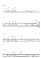
のマイクロボール3と、半導体素子4とマイクロボール3を電気的に接続する金属ワイヤ5と、半導体素子4、マイクロボール3の一部、および金属ワイヤ5とを絶縁樹脂7で封止する封止体とを備えている。図1(b)に示すように、半導体素子4の裏面は、封止体の底面と一平面をなすように露出し、外部端子としてマイクロボール3の少なくとも一部は、封止体の裏面から突出した露出部を有している。マイクロボール3は、封止体内の半導体素子4との内部接続用配線の役割と、実装基板との接続に用いる外部接続用端子としての役割を兼ね備えている。
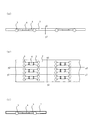
初めに図3(a)に示されるようにステンレス、銅などの導電性金属薄板1あるいは耐熱ゴム薄板または樹脂薄板を用いる。例えば本実施例の場合は、1.0mm厚のステンレス薄板にレーザー加工により円柱形の開口部2を形成した薄板1を準備する。開口部にはテーパを施し面取り加工を施す。ここで図3(a)は上面図、図3(b)は図3(a)のx1−x1断面図である。
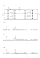
の上端面が樹脂封止金型(上型)と接触し、マイクロボールに押付け圧力が負荷された状態で絶縁樹脂7を薄板1上に片面封止することにより形成する。ここでは、エポキシ樹脂を用いたトランスファモールド法により行う。実施例2の樹脂封止型半導体装置は図7(b)に示されるとおり樹脂封止金型に接触したマイクロボール3の上端面が露出する形態となる。
初めに図9(a)に示されるようにステンレス、銅などの導電性金属薄板1あるいは耐熱ゴム、樹脂薄板を用い、例えば本実施例の場合は、0.08mm厚の銅薄板にパンチを用いたプレス加工により円柱形の開口部2を形成する。開口部にはテーパを施し面取り加工を施してもよい。図9(a)は上面図、図9(b)〜図9(j)は、図9(a)のx2−x2で示される位置における工程順の断面図である。
の際は前項のとおりマイクロボール3がテープ8を介して薄板1に固定された状態で行われ、ここでは、トランスファモールド法により、樹脂封止金型6内に絶縁樹脂7を注入する。絶縁樹脂を封止する際には、トランスファモールド法の代わりに、ポッティング法を用いても良い。実施例3の樹脂封止型半導体装置は図11(j)に示されるとおり絶縁樹脂7内にマイクロボール3がボールの下端面を除いて埋め込まれる形態となる。
の際は前項のとおりマイクロボール3がテープ8を介して薄板1に固定された状態で行われ、ここでは、トランスファモールド法により、樹脂封止金型6内に絶縁樹脂7を注入する。絶縁樹脂を封止する際には、トランスファモールド法の代わりに、ポッティング法を用いても良い。実施例4の樹脂封止型半導体装置は図15(j)に示されるとおり絶縁樹脂7内にマイクロボール3がボールの下端面を除いて埋め込まれる形態となる。
2 開口部
3 マイクロボール
4 半導体素子
5 金属ワイヤ
6 樹脂封止金型
7 絶縁樹脂
8 テープ
9 ローラー
Claims (7)
- 半導体素子と、内部端子面と外部端子面を表裏一体に備える複数のマイクロボールと、前記半導体素子と前記内部端子面とを電気的に接続する金属ワイヤと、前記半導体素子、前記複数のマイクロボールの一部、および、前記ワイヤを封止樹脂で封止する封止体とを備えた樹脂封止型半導体装置において、
前記マイクロボールがプラスチックの粒子表面に金属メッキを施したボールであり、前記金属メッキは単一組成のメッキもしくは多層組成のメッキにより形成され、前記半導体素子の裏面が前記封止体から露出し、かつ、前記複数のマイクロボールの一部が前記外部端子面として前記封止体の底面から突起状に露出していることを特徴とする樹脂封止型半導体装置。 - 前記半導体素子の裏面が、前記封止体底面と一平面をなすように露出形成されることを特徴とする請求項1に記載の樹脂封止型半導体装置。
- 前記半導体素子の裏面と前記マイクロボールの少なくとも一部が、前記封止体の底面と一平面をなすように露出形成されることを特徴とする請求項1に記載の樹脂封止型半導体装置。
- 前記マイクロボールが、前記封止体の上面および底面から露出形成されることを特徴とする請求項1に記載の樹脂封止型半導体装置。
- 前記マイクロボールの外部露出部が、前記封止体底面から前記マイクロボールの半径以下の寸法で突出形成されることを特徴とする請求項1に記載の樹脂封止型半導体装置。
- 前記マイクロボールが金属ボールであり、前記金属ボールは単一材料もしくは多種の材料により積層形成されることを特徴とする請求項1に記載の樹脂封止型半導体装置。
- 半導体素子と
前記半導体素子の周囲に配置された複数のマイクロボールと、
前記半導体素子と、前記複数のマイクロボールのそれぞれの第1の部分である内部端子面とを電気的に接続する金属ワイヤと、
前記半導体素子、前記複数のマイクロボールのそれぞれの所望の領域、および、前記ワイヤを封止樹脂で封止する封止体とからなり、
前記マイクロボールがプラスチックの粒子表面に金属メッキを施したボールであり、前記金属メッキは単一組成のメッキもしくは多層組成のメッキにより形成され、
前記半導体素子の裏面が前記封止体から露出し、前記複数のマイクロボールのそれぞれの第2の部分が外部端子面として前記封止体の底面から突起状に露出している樹脂封止型半導体装置。
Priority Applications (6)
| Application Number | Priority Date | Filing Date | Title |
|---|---|---|---|
| JP2009258415A JP5588150B2 (ja) | 2009-02-06 | 2009-11-11 | 樹脂封止型半導体装置 |
| TW099101642A TWI478296B (zh) | 2009-02-06 | 2010-01-21 | 樹脂密封型半導體裝置 |
| CN201010113656.6A CN101901788B (zh) | 2009-02-06 | 2010-02-05 | 树脂密封型半导体装置及其制造方法 |
| US12/701,018 US8703532B2 (en) | 2009-02-06 | 2010-02-05 | Semiconductor device and manufacturing method thereof |
| KR1020100011105A KR101665963B1 (ko) | 2009-02-06 | 2010-02-05 | 수지 봉지형 반도체 장치 및 그 제조 방법 |
| US14/150,153 US9490224B2 (en) | 2009-02-06 | 2014-01-08 | Semiconductor device and manufacturing method thereof |
Applications Claiming Priority (3)
| Application Number | Priority Date | Filing Date | Title |
|---|---|---|---|
| JP2009026507 | 2009-02-06 | ||
| JP2009026507 | 2009-02-06 | ||
| JP2009258415A JP5588150B2 (ja) | 2009-02-06 | 2009-11-11 | 樹脂封止型半導体装置 |
Publications (3)
| Publication Number | Publication Date |
|---|---|
| JP2010206162A JP2010206162A (ja) | 2010-09-16 |
| JP2010206162A5 JP2010206162A5 (ja) | 2012-10-25 |
| JP5588150B2 true JP5588150B2 (ja) | 2014-09-10 |
Family
ID=42539745
Family Applications (1)
| Application Number | Title | Priority Date | Filing Date |
|---|---|---|---|
| JP2009258415A Expired - Fee Related JP5588150B2 (ja) | 2009-02-06 | 2009-11-11 | 樹脂封止型半導体装置 |
Country Status (5)
| Country | Link |
|---|---|
| US (2) | US8703532B2 (ja) |
| JP (1) | JP5588150B2 (ja) |
| KR (1) | KR101665963B1 (ja) |
| CN (1) | CN101901788B (ja) |
| TW (1) | TWI478296B (ja) |
Families Citing this family (8)
| Publication number | Priority date | Publication date | Assignee | Title |
|---|---|---|---|---|
| JP5642473B2 (ja) * | 2010-09-22 | 2014-12-17 | セイコーインスツル株式会社 | Bga半導体パッケージおよびその製造方法 |
| CN102786028B (zh) * | 2012-07-17 | 2015-05-06 | 西南交通大学 | 一种用于大面积摩擦诱导微/纳米加工的多针尖阵列的制作方法 |
| CN102832141A (zh) * | 2012-08-18 | 2012-12-19 | 孙青秀 | 一种基于框架的无载体式封装件的制作工艺 |
| TWM506375U (zh) * | 2013-07-03 | 2015-08-01 | Rosenberger Hochfrequenztech | 使用介電質塗層引線的晶粒封裝 |
| DE102015212177A1 (de) * | 2015-06-30 | 2017-01-05 | Osram Gmbh | Schaltungsträger für eine elektronische Schaltung und Verfahren zum Herstellen eines derartigen Schaltungsträgers |
| CN105489509A (zh) * | 2015-12-25 | 2016-04-13 | 华天科技(西安)有限公司 | 应用钢网印刷技术优化点胶工艺的光学传感芯片封装方法 |
| CN110517963A (zh) * | 2019-09-05 | 2019-11-29 | 合肥矽迈微电子科技有限公司 | 一种环膜结构注塑工艺 |
| JPWO2021049235A1 (ja) * | 2019-09-13 | 2021-03-18 |
Family Cites Families (19)
| Publication number | Priority date | Publication date | Assignee | Title |
|---|---|---|---|---|
| JP3129169B2 (ja) * | 1995-11-08 | 2001-01-29 | 富士通株式会社 | 半導体装置及びその製造方法 |
| KR100332378B1 (ko) * | 1999-09-11 | 2002-04-12 | 이병구 | 반도체 패키지의 솔더볼 마운팅 방법 |
| JP3823651B2 (ja) * | 2000-01-05 | 2006-09-20 | 松下電器産業株式会社 | 樹脂封止型半導体装置の製造方法 |
| JP2001230270A (ja) * | 2000-02-14 | 2001-08-24 | Fujitsu Ltd | 半導体装置及びその製造方法 |
| JP3626075B2 (ja) | 2000-06-20 | 2005-03-02 | 九州日立マクセル株式会社 | 半導体装置の製造方法 |
| US20020033527A1 (en) * | 2000-09-19 | 2002-03-21 | Siliconware Precision Industries Co., Ltd. | Semiconductor device and manufacturing process thereof |
| US7297572B2 (en) * | 2001-09-07 | 2007-11-20 | Hynix Semiconductor, Inc. | Fabrication method for electronic system modules |
| JP4014912B2 (ja) * | 2001-09-28 | 2007-11-28 | 株式会社ルネサステクノロジ | 半導体装置 |
| CN1477703A (zh) * | 2002-08-02 | 2004-02-25 | 千住金属工业株式会社 | 焊球组件及其生产方法,形成焊块的方法 |
| JP2004319577A (ja) * | 2003-04-11 | 2004-11-11 | Dainippon Printing Co Ltd | 樹脂封止型半導体装置とその製造方法、および積層型樹脂封止型半導体装置 |
| US7056766B2 (en) * | 2003-12-09 | 2006-06-06 | Freescale Semiconductor, Inc. | Method of forming land grid array packaged device |
| JP2005194393A (ja) * | 2004-01-07 | 2005-07-21 | Hitachi Chem Co Ltd | 回路接続用接着フィルム及び回路接続構造体 |
| KR20050079399A (ko) * | 2004-02-05 | 2005-08-10 | 삼성전자주식회사 | 이방성도전필름 및 범프와, 이를 갖는 반도체 칩의 실장구조체 |
| US7205178B2 (en) * | 2004-03-24 | 2007-04-17 | Freescale Semiconductor, Inc. | Land grid array packaged device and method of forming same |
| JP2006066521A (ja) * | 2004-08-25 | 2006-03-09 | Fujitsu Ltd | 半導体装置及び半導体装置の製造方法 |
| US8169067B2 (en) * | 2006-10-20 | 2012-05-01 | Broadcom Corporation | Low profile ball grid array (BGA) package with exposed die and method of making same |
| KR100792663B1 (ko) * | 2006-12-01 | 2008-01-09 | 주식회사 동부하이텍 | 다층구조의 금속층으로 적층된 전자패키지용 플라스틱솔더볼의 제조방법 및 그로부터 제조된 플라스틱 솔더볼 |
| TW200903756A (en) * | 2007-06-18 | 2009-01-16 | Samsung Electronics Co Ltd | Semiconductor chip package, semiconductor package including semiconductor chip package, and method of fabricating semiconductor package |
| US8501088B2 (en) * | 2007-07-25 | 2013-08-06 | Nippon Steel & Sumikin Materials Co., Ltd. | Solder alloy, solder ball and electronic member having solder bump |
-
2009
- 2009-11-11 JP JP2009258415A patent/JP5588150B2/ja not_active Expired - Fee Related
-
2010
- 2010-01-21 TW TW099101642A patent/TWI478296B/zh not_active IP Right Cessation
- 2010-02-05 US US12/701,018 patent/US8703532B2/en not_active Expired - Fee Related
- 2010-02-05 KR KR1020100011105A patent/KR101665963B1/ko active IP Right Grant
- 2010-02-05 CN CN201010113656.6A patent/CN101901788B/zh not_active Expired - Fee Related
-
2014
- 2014-01-08 US US14/150,153 patent/US9490224B2/en active Active
Also Published As
| Publication number | Publication date |
|---|---|
| US8703532B2 (en) | 2014-04-22 |
| US9490224B2 (en) | 2016-11-08 |
| TW201036118A (en) | 2010-10-01 |
| KR101665963B1 (ko) | 2016-10-24 |
| US20100200982A1 (en) | 2010-08-12 |
| KR20100090666A (ko) | 2010-08-16 |
| TWI478296B (zh) | 2015-03-21 |
| CN101901788A (zh) | 2010-12-01 |
| CN101901788B (zh) | 2014-10-29 |
| US20140117544A1 (en) | 2014-05-01 |
| JP2010206162A (ja) | 2010-09-16 |
Similar Documents
| Publication | Publication Date | Title |
|---|---|---|
| JP5588150B2 (ja) | 樹脂封止型半導体装置 | |
| US6909178B2 (en) | Semiconductor device and method of manufacturing the same | |
| US20080023819A1 (en) | Package structure having semiconductor chip embedded therein and method for fabricating the same | |
| US8211754B2 (en) | Semiconductor device and manufacturing method thereof | |
| KR20080049760A (ko) | 반도체 장치 및 그 제조 방법 | |
| JP2013069807A (ja) | 半導体パッケージ及びその製造方法 | |
| US9245864B2 (en) | Ball grid array semiconductor package and method of manufacturing the same | |
| JP2021027116A (ja) | 半導体装置 | |
| TW201631715A (zh) | 佈線基板、製造佈線基板之方法及電子組件裝置 | |
| JP6964477B2 (ja) | 半導体素子用基板及びその製造方法、半導体装置及びその製造方法 | |
| JP4379693B2 (ja) | 半導体装置およびその製造方法 | |
| JP4970388B2 (ja) | 半導体装置及び半導体装置の製造方法 | |
| WO2007057954A1 (ja) | 半導体装置及びその製造方法 | |
| JP3925503B2 (ja) | 半導体装置 | |
| KR20040030301A (ko) | 회로 장치의 제조 방법 | |
| JP2956659B2 (ja) | 半導体装置およびそのリードフレーム | |
| JP4577316B2 (ja) | 半導体装置の製造方法 | |
| JP4979661B2 (ja) | 半導体装置の製造方法 | |
| JP4089629B2 (ja) | 光センサモジュール | |
| JP4321758B2 (ja) | 半導体装置 | |
| JP2003046053A (ja) | 半導体装置およびその製造方法 | |
| JP2005116886A (ja) | 半導体装置の製造方法 | |
| JPH0738015A (ja) | 樹脂封止型半導体装置およびその製造方法 | |
| JP2009302427A (ja) | 半導体装置および半導体装置の製造方法 | |
| JP2005044931A (ja) | 半導体搭載用基板製造方法、半導体パッケージ製造方法、半導体搭載用基板及び半導体パッケージ |
Legal Events
| Date | Code | Title | Description |
|---|---|---|---|
| A521 | Request for written amendment filed |
Free format text: JAPANESE INTERMEDIATE CODE: A523 Effective date: 20120911 |
|
| A621 | Written request for application examination |
Free format text: JAPANESE INTERMEDIATE CODE: A621 Effective date: 20120911 |
|
| A977 | Report on retrieval |
Free format text: JAPANESE INTERMEDIATE CODE: A971007 Effective date: 20130513 |
|
| A131 | Notification of reasons for refusal |
Free format text: JAPANESE INTERMEDIATE CODE: A131 Effective date: 20130521 |
|
| A521 | Request for written amendment filed |
Free format text: JAPANESE INTERMEDIATE CODE: A523 Effective date: 20130718 |
|
| A131 | Notification of reasons for refusal |
Free format text: JAPANESE INTERMEDIATE CODE: A131 Effective date: 20140415 |
|
| A521 | Request for written amendment filed |
Free format text: JAPANESE INTERMEDIATE CODE: A523 Effective date: 20140612 |
|
| TRDD | Decision of grant or rejection written | ||
| A01 | Written decision to grant a patent or to grant a registration (utility model) |
Free format text: JAPANESE INTERMEDIATE CODE: A01 Effective date: 20140701 |
|
| A61 | First payment of annual fees (during grant procedure) |
Free format text: JAPANESE INTERMEDIATE CODE: A61 Effective date: 20140725 |
|
| R150 | Certificate of patent or registration of utility model |
Ref document number: 5588150 Country of ref document: JP Free format text: JAPANESE INTERMEDIATE CODE: R150 |
|
| S111 | Request for change of ownership or part of ownership |
Free format text: JAPANESE INTERMEDIATE CODE: R313113 |
|
| R350 | Written notification of registration of transfer |
Free format text: JAPANESE INTERMEDIATE CODE: R350 |
|
| R250 | Receipt of annual fees |
Free format text: JAPANESE INTERMEDIATE CODE: R250 |
|
| S533 | Written request for registration of change of name |
Free format text: JAPANESE INTERMEDIATE CODE: R313533 |
|
| R350 | Written notification of registration of transfer |
Free format text: JAPANESE INTERMEDIATE CODE: R350 |
|
| R250 | Receipt of annual fees |
Free format text: JAPANESE INTERMEDIATE CODE: R250 |
|
| R250 | Receipt of annual fees |
Free format text: JAPANESE INTERMEDIATE CODE: R250 |
|
| R250 | Receipt of annual fees |
Free format text: JAPANESE INTERMEDIATE CODE: R250 |
|
| LAPS | Cancellation because of no payment of annual fees |