JP5588150B2 - Resin-sealed semiconductor device - Google Patents
Resin-sealed semiconductor device Download PDFInfo
- Publication number
- JP5588150B2 JP5588150B2 JP2009258415A JP2009258415A JP5588150B2 JP 5588150 B2 JP5588150 B2 JP 5588150B2 JP 2009258415 A JP2009258415 A JP 2009258415A JP 2009258415 A JP2009258415 A JP 2009258415A JP 5588150 B2 JP5588150 B2 JP 5588150B2
- Authority
- JP
- Japan
- Prior art keywords
- resin
- semiconductor element
- microball
- semiconductor device
- sealing body
- Prior art date
- Legal status (The legal status is an assumption and is not a legal conclusion. Google has not performed a legal analysis and makes no representation as to the accuracy of the status listed.)
- Expired - Fee Related
Links
Images


Classifications
-
- H—ELECTRICITY
- H01—ELECTRIC ELEMENTS
- H01L—SEMICONDUCTOR DEVICES NOT COVERED BY CLASS H10
- H01L24/00—Arrangements for connecting or disconnecting semiconductor or solid-state bodies; Methods or apparatus related thereto
- H01L24/01—Means for bonding being attached to, or being formed on, the surface to be connected, e.g. chip-to-package, die-attach, "first-level" interconnects; Manufacturing methods related thereto
- H01L24/10—Bump connectors ; Manufacturing methods related thereto
- H01L24/12—Structure, shape, material or disposition of the bump connectors prior to the connecting process
- H01L24/14—Structure, shape, material or disposition of the bump connectors prior to the connecting process of a plurality of bump connectors
-
- H—ELECTRICITY
- H01—ELECTRIC ELEMENTS
- H01L—SEMICONDUCTOR DEVICES NOT COVERED BY CLASS H10
- H01L21/00—Processes or apparatus adapted for the manufacture or treatment of semiconductor or solid state devices or of parts thereof
- H01L21/02—Manufacture or treatment of semiconductor devices or of parts thereof
- H01L21/04—Manufacture or treatment of semiconductor devices or of parts thereof the devices having at least one potential-jump barrier or surface barrier, e.g. PN junction, depletion layer or carrier concentration layer
- H01L21/50—Assembly of semiconductor devices using processes or apparatus not provided for in a single one of the subgroups H01L21/06 - H01L21/326, e.g. sealing of a cap to a base of a container
- H01L21/56—Encapsulations, e.g. encapsulation layers, coatings
- H01L21/561—Batch processing
-
- H—ELECTRICITY
- H01—ELECTRIC ELEMENTS
- H01L—SEMICONDUCTOR DEVICES NOT COVERED BY CLASS H10
- H01L21/00—Processes or apparatus adapted for the manufacture or treatment of semiconductor or solid state devices or of parts thereof
- H01L21/02—Manufacture or treatment of semiconductor devices or of parts thereof
- H01L21/04—Manufacture or treatment of semiconductor devices or of parts thereof the devices having at least one potential-jump barrier or surface barrier, e.g. PN junction, depletion layer or carrier concentration layer
- H01L21/50—Assembly of semiconductor devices using processes or apparatus not provided for in a single one of the subgroups H01L21/06 - H01L21/326, e.g. sealing of a cap to a base of a container
- H01L21/56—Encapsulations, e.g. encapsulation layers, coatings
- H01L21/565—Moulds
-
- H—ELECTRICITY
- H01—ELECTRIC ELEMENTS
- H01L—SEMICONDUCTOR DEVICES NOT COVERED BY CLASS H10
- H01L21/00—Processes or apparatus adapted for the manufacture or treatment of semiconductor or solid state devices or of parts thereof
- H01L21/02—Manufacture or treatment of semiconductor devices or of parts thereof
- H01L21/04—Manufacture or treatment of semiconductor devices or of parts thereof the devices having at least one potential-jump barrier or surface barrier, e.g. PN junction, depletion layer or carrier concentration layer
- H01L21/50—Assembly of semiconductor devices using processes or apparatus not provided for in a single one of the subgroups H01L21/06 - H01L21/326, e.g. sealing of a cap to a base of a container
- H01L21/56—Encapsulations, e.g. encapsulation layers, coatings
- H01L21/568—Temporary substrate used as encapsulation process aid
-
- H—ELECTRICITY
- H01—ELECTRIC ELEMENTS
- H01L—SEMICONDUCTOR DEVICES NOT COVERED BY CLASS H10
- H01L23/00—Details of semiconductor or other solid state devices
- H01L23/28—Encapsulations, e.g. encapsulating layers, coatings, e.g. for protection
- H01L23/31—Encapsulations, e.g. encapsulating layers, coatings, e.g. for protection characterised by the arrangement or shape
- H01L23/3107—Encapsulations, e.g. encapsulating layers, coatings, e.g. for protection characterised by the arrangement or shape the device being completely enclosed
-
- H—ELECTRICITY
- H01—ELECTRIC ELEMENTS
- H01L—SEMICONDUCTOR DEVICES NOT COVERED BY CLASS H10
- H01L24/00—Arrangements for connecting or disconnecting semiconductor or solid-state bodies; Methods or apparatus related thereto
- H01L24/01—Means for bonding being attached to, or being formed on, the surface to be connected, e.g. chip-to-package, die-attach, "first-level" interconnects; Manufacturing methods related thereto
- H01L24/42—Wire connectors; Manufacturing methods related thereto
- H01L24/47—Structure, shape, material or disposition of the wire connectors after the connecting process
- H01L24/48—Structure, shape, material or disposition of the wire connectors after the connecting process of an individual wire connector
-
- H—ELECTRICITY
- H01—ELECTRIC ELEMENTS
- H01L—SEMICONDUCTOR DEVICES NOT COVERED BY CLASS H10
- H01L24/00—Arrangements for connecting or disconnecting semiconductor or solid-state bodies; Methods or apparatus related thereto
- H01L24/01—Means for bonding being attached to, or being formed on, the surface to be connected, e.g. chip-to-package, die-attach, "first-level" interconnects; Manufacturing methods related thereto
- H01L24/42—Wire connectors; Manufacturing methods related thereto
- H01L24/47—Structure, shape, material or disposition of the wire connectors after the connecting process
- H01L24/49—Structure, shape, material or disposition of the wire connectors after the connecting process of a plurality of wire connectors
-
- H—ELECTRICITY
- H01—ELECTRIC ELEMENTS
- H01L—SEMICONDUCTOR DEVICES NOT COVERED BY CLASS H10
- H01L24/00—Arrangements for connecting or disconnecting semiconductor or solid-state bodies; Methods or apparatus related thereto
- H01L24/93—Batch processes
- H01L24/95—Batch processes at chip-level, i.e. with connecting carried out on a plurality of singulated devices, i.e. on diced chips
- H01L24/97—Batch processes at chip-level, i.e. with connecting carried out on a plurality of singulated devices, i.e. on diced chips the devices being connected to a common substrate, e.g. interposer, said common substrate being separable into individual assemblies after connecting
-
- H—ELECTRICITY
- H01—ELECTRIC ELEMENTS
- H01L—SEMICONDUCTOR DEVICES NOT COVERED BY CLASS H10
- H01L2224/00—Indexing scheme for arrangements for connecting or disconnecting semiconductor or solid-state bodies and methods related thereto as covered by H01L24/00
- H01L2224/01—Means for bonding being attached to, or being formed on, the surface to be connected, e.g. chip-to-package, die-attach, "first-level" interconnects; Manufacturing methods related thereto
- H01L2224/02—Bonding areas; Manufacturing methods related thereto
- H01L2224/04—Structure, shape, material or disposition of the bonding areas prior to the connecting process
- H01L2224/05—Structure, shape, material or disposition of the bonding areas prior to the connecting process of an individual bonding area
- H01L2224/0554—External layer
- H01L2224/0555—Shape
- H01L2224/05552—Shape in top view
- H01L2224/05554—Shape in top view being square
-
- H—ELECTRICITY
- H01—ELECTRIC ELEMENTS
- H01L—SEMICONDUCTOR DEVICES NOT COVERED BY CLASS H10
- H01L2224/00—Indexing scheme for arrangements for connecting or disconnecting semiconductor or solid-state bodies and methods related thereto as covered by H01L24/00
- H01L2224/01—Means for bonding being attached to, or being formed on, the surface to be connected, e.g. chip-to-package, die-attach, "first-level" interconnects; Manufacturing methods related thereto
- H01L2224/42—Wire connectors; Manufacturing methods related thereto
- H01L2224/44—Structure, shape, material or disposition of the wire connectors prior to the connecting process
- H01L2224/45—Structure, shape, material or disposition of the wire connectors prior to the connecting process of an individual wire connector
- H01L2224/45001—Core members of the connector
- H01L2224/4501—Shape
- H01L2224/45012—Cross-sectional shape
- H01L2224/45015—Cross-sectional shape being circular
-
- H—ELECTRICITY
- H01—ELECTRIC ELEMENTS
- H01L—SEMICONDUCTOR DEVICES NOT COVERED BY CLASS H10
- H01L2224/00—Indexing scheme for arrangements for connecting or disconnecting semiconductor or solid-state bodies and methods related thereto as covered by H01L24/00
- H01L2224/01—Means for bonding being attached to, or being formed on, the surface to be connected, e.g. chip-to-package, die-attach, "first-level" interconnects; Manufacturing methods related thereto
- H01L2224/42—Wire connectors; Manufacturing methods related thereto
- H01L2224/44—Structure, shape, material or disposition of the wire connectors prior to the connecting process
- H01L2224/45—Structure, shape, material or disposition of the wire connectors prior to the connecting process of an individual wire connector
- H01L2224/45001—Core members of the connector
- H01L2224/45099—Material
- H01L2224/451—Material with a principal constituent of the material being a metal or a metalloid, e.g. boron (B), silicon (Si), germanium (Ge), arsenic (As), antimony (Sb), tellurium (Te) and polonium (Po), and alloys thereof
- H01L2224/45117—Material with a principal constituent of the material being a metal or a metalloid, e.g. boron (B), silicon (Si), germanium (Ge), arsenic (As), antimony (Sb), tellurium (Te) and polonium (Po), and alloys thereof the principal constituent melting at a temperature of greater than or equal to 400°C and less than 950°C
- H01L2224/45124—Aluminium (Al) as principal constituent
-
- H—ELECTRICITY
- H01—ELECTRIC ELEMENTS
- H01L—SEMICONDUCTOR DEVICES NOT COVERED BY CLASS H10
- H01L2224/00—Indexing scheme for arrangements for connecting or disconnecting semiconductor or solid-state bodies and methods related thereto as covered by H01L24/00
- H01L2224/01—Means for bonding being attached to, or being formed on, the surface to be connected, e.g. chip-to-package, die-attach, "first-level" interconnects; Manufacturing methods related thereto
- H01L2224/42—Wire connectors; Manufacturing methods related thereto
- H01L2224/44—Structure, shape, material or disposition of the wire connectors prior to the connecting process
- H01L2224/45—Structure, shape, material or disposition of the wire connectors prior to the connecting process of an individual wire connector
- H01L2224/45001—Core members of the connector
- H01L2224/45099—Material
- H01L2224/451—Material with a principal constituent of the material being a metal or a metalloid, e.g. boron (B), silicon (Si), germanium (Ge), arsenic (As), antimony (Sb), tellurium (Te) and polonium (Po), and alloys thereof
- H01L2224/45138—Material with a principal constituent of the material being a metal or a metalloid, e.g. boron (B), silicon (Si), germanium (Ge), arsenic (As), antimony (Sb), tellurium (Te) and polonium (Po), and alloys thereof the principal constituent melting at a temperature of greater than or equal to 950°C and less than 1550°C
- H01L2224/45144—Gold (Au) as principal constituent
-
- H—ELECTRICITY
- H01—ELECTRIC ELEMENTS
- H01L—SEMICONDUCTOR DEVICES NOT COVERED BY CLASS H10
- H01L2224/00—Indexing scheme for arrangements for connecting or disconnecting semiconductor or solid-state bodies and methods related thereto as covered by H01L24/00
- H01L2224/01—Means for bonding being attached to, or being formed on, the surface to be connected, e.g. chip-to-package, die-attach, "first-level" interconnects; Manufacturing methods related thereto
- H01L2224/42—Wire connectors; Manufacturing methods related thereto
- H01L2224/44—Structure, shape, material or disposition of the wire connectors prior to the connecting process
- H01L2224/45—Structure, shape, material or disposition of the wire connectors prior to the connecting process of an individual wire connector
- H01L2224/45001—Core members of the connector
- H01L2224/45099—Material
- H01L2224/451—Material with a principal constituent of the material being a metal or a metalloid, e.g. boron (B), silicon (Si), germanium (Ge), arsenic (As), antimony (Sb), tellurium (Te) and polonium (Po), and alloys thereof
- H01L2224/45138—Material with a principal constituent of the material being a metal or a metalloid, e.g. boron (B), silicon (Si), germanium (Ge), arsenic (As), antimony (Sb), tellurium (Te) and polonium (Po), and alloys thereof the principal constituent melting at a temperature of greater than or equal to 950°C and less than 1550°C
- H01L2224/45147—Copper (Cu) as principal constituent
-
- H—ELECTRICITY
- H01—ELECTRIC ELEMENTS
- H01L—SEMICONDUCTOR DEVICES NOT COVERED BY CLASS H10
- H01L2224/00—Indexing scheme for arrangements for connecting or disconnecting semiconductor or solid-state bodies and methods related thereto as covered by H01L24/00
- H01L2224/01—Means for bonding being attached to, or being formed on, the surface to be connected, e.g. chip-to-package, die-attach, "first-level" interconnects; Manufacturing methods related thereto
- H01L2224/42—Wire connectors; Manufacturing methods related thereto
- H01L2224/47—Structure, shape, material or disposition of the wire connectors after the connecting process
- H01L2224/48—Structure, shape, material or disposition of the wire connectors after the connecting process of an individual wire connector
- H01L2224/4805—Shape
- H01L2224/4809—Loop shape
- H01L2224/48091—Arched
-
- H—ELECTRICITY
- H01—ELECTRIC ELEMENTS
- H01L—SEMICONDUCTOR DEVICES NOT COVERED BY CLASS H10
- H01L2224/00—Indexing scheme for arrangements for connecting or disconnecting semiconductor or solid-state bodies and methods related thereto as covered by H01L24/00
- H01L2224/01—Means for bonding being attached to, or being formed on, the surface to be connected, e.g. chip-to-package, die-attach, "first-level" interconnects; Manufacturing methods related thereto
- H01L2224/42—Wire connectors; Manufacturing methods related thereto
- H01L2224/47—Structure, shape, material or disposition of the wire connectors after the connecting process
- H01L2224/48—Structure, shape, material or disposition of the wire connectors after the connecting process of an individual wire connector
- H01L2224/484—Connecting portions
- H01L2224/48463—Connecting portions the connecting portion on the bonding area of the semiconductor or solid-state body being a ball bond
- H01L2224/48465—Connecting portions the connecting portion on the bonding area of the semiconductor or solid-state body being a ball bond the other connecting portion not on the bonding area being a wedge bond, i.e. ball-to-wedge, regular stitch
-
- H—ELECTRICITY
- H01—ELECTRIC ELEMENTS
- H01L—SEMICONDUCTOR DEVICES NOT COVERED BY CLASS H10
- H01L2224/00—Indexing scheme for arrangements for connecting or disconnecting semiconductor or solid-state bodies and methods related thereto as covered by H01L24/00
- H01L2224/01—Means for bonding being attached to, or being formed on, the surface to be connected, e.g. chip-to-package, die-attach, "first-level" interconnects; Manufacturing methods related thereto
- H01L2224/42—Wire connectors; Manufacturing methods related thereto
- H01L2224/47—Structure, shape, material or disposition of the wire connectors after the connecting process
- H01L2224/48—Structure, shape, material or disposition of the wire connectors after the connecting process of an individual wire connector
- H01L2224/485—Material
- H01L2224/48505—Material at the bonding interface
- H01L2224/48599—Principal constituent of the connecting portion of the wire connector being Gold (Au)
-
- H—ELECTRICITY
- H01—ELECTRIC ELEMENTS
- H01L—SEMICONDUCTOR DEVICES NOT COVERED BY CLASS H10
- H01L2224/00—Indexing scheme for arrangements for connecting or disconnecting semiconductor or solid-state bodies and methods related thereto as covered by H01L24/00
- H01L2224/01—Means for bonding being attached to, or being formed on, the surface to be connected, e.g. chip-to-package, die-attach, "first-level" interconnects; Manufacturing methods related thereto
- H01L2224/42—Wire connectors; Manufacturing methods related thereto
- H01L2224/47—Structure, shape, material or disposition of the wire connectors after the connecting process
- H01L2224/48—Structure, shape, material or disposition of the wire connectors after the connecting process of an individual wire connector
- H01L2224/485—Material
- H01L2224/48505—Material at the bonding interface
- H01L2224/48699—Principal constituent of the connecting portion of the wire connector being Aluminium (Al)
-
- H—ELECTRICITY
- H01—ELECTRIC ELEMENTS
- H01L—SEMICONDUCTOR DEVICES NOT COVERED BY CLASS H10
- H01L2224/00—Indexing scheme for arrangements for connecting or disconnecting semiconductor or solid-state bodies and methods related thereto as covered by H01L24/00
- H01L2224/01—Means for bonding being attached to, or being formed on, the surface to be connected, e.g. chip-to-package, die-attach, "first-level" interconnects; Manufacturing methods related thereto
- H01L2224/42—Wire connectors; Manufacturing methods related thereto
- H01L2224/47—Structure, shape, material or disposition of the wire connectors after the connecting process
- H01L2224/49—Structure, shape, material or disposition of the wire connectors after the connecting process of a plurality of wire connectors
- H01L2224/491—Disposition
- H01L2224/4912—Layout
- H01L2224/49171—Fan-out arrangements
-
- H—ELECTRICITY
- H01—ELECTRIC ELEMENTS
- H01L—SEMICONDUCTOR DEVICES NOT COVERED BY CLASS H10
- H01L2224/00—Indexing scheme for arrangements for connecting or disconnecting semiconductor or solid-state bodies and methods related thereto as covered by H01L24/00
- H01L2224/80—Methods for connecting semiconductor or other solid state bodies using means for bonding being attached to, or being formed on, the surface to be connected
- H01L2224/85—Methods for connecting semiconductor or other solid state bodies using means for bonding being attached to, or being formed on, the surface to be connected using a wire connector
- H01L2224/85001—Methods for connecting semiconductor or other solid state bodies using means for bonding being attached to, or being formed on, the surface to be connected using a wire connector involving a temporary auxiliary member not forming part of the bonding apparatus, e.g. removable or sacrificial coating, film or substrate
-
- H—ELECTRICITY
- H01—ELECTRIC ELEMENTS
- H01L—SEMICONDUCTOR DEVICES NOT COVERED BY CLASS H10
- H01L2224/00—Indexing scheme for arrangements for connecting or disconnecting semiconductor or solid-state bodies and methods related thereto as covered by H01L24/00
- H01L2224/80—Methods for connecting semiconductor or other solid state bodies using means for bonding being attached to, or being formed on, the surface to be connected
- H01L2224/85—Methods for connecting semiconductor or other solid state bodies using means for bonding being attached to, or being formed on, the surface to be connected using a wire connector
- H01L2224/8538—Bonding interfaces outside the semiconductor or solid-state body
- H01L2224/85399—Material
- H01L2224/854—Material with a principal constituent of the material being a metal or a metalloid, e.g. boron (B), silicon (Si), germanium (Ge), arsenic (As), antimony (Sb), tellurium (Te) and polonium (Po), and alloys thereof
- H01L2224/85417—Material with a principal constituent of the material being a metal or a metalloid, e.g. boron (B), silicon (Si), germanium (Ge), arsenic (As), antimony (Sb), tellurium (Te) and polonium (Po), and alloys thereof the principal constituent melting at a temperature of greater than or equal to 400°C and less than 950°C
- H01L2224/85423—Magnesium (Mg) as principal constituent
-
- H—ELECTRICITY
- H01—ELECTRIC ELEMENTS
- H01L—SEMICONDUCTOR DEVICES NOT COVERED BY CLASS H10
- H01L2224/00—Indexing scheme for arrangements for connecting or disconnecting semiconductor or solid-state bodies and methods related thereto as covered by H01L24/00
- H01L2224/80—Methods for connecting semiconductor or other solid state bodies using means for bonding being attached to, or being formed on, the surface to be connected
- H01L2224/85—Methods for connecting semiconductor or other solid state bodies using means for bonding being attached to, or being formed on, the surface to be connected using a wire connector
- H01L2224/8538—Bonding interfaces outside the semiconductor or solid-state body
- H01L2224/85399—Material
- H01L2224/854—Material with a principal constituent of the material being a metal or a metalloid, e.g. boron (B), silicon (Si), germanium (Ge), arsenic (As), antimony (Sb), tellurium (Te) and polonium (Po), and alloys thereof
- H01L2224/85438—Material with a principal constituent of the material being a metal or a metalloid, e.g. boron (B), silicon (Si), germanium (Ge), arsenic (As), antimony (Sb), tellurium (Te) and polonium (Po), and alloys thereof the principal constituent melting at a temperature of greater than or equal to 950°C and less than 1550°C
- H01L2224/85439—Silver (Ag) as principal constituent
-
- H—ELECTRICITY
- H01—ELECTRIC ELEMENTS
- H01L—SEMICONDUCTOR DEVICES NOT COVERED BY CLASS H10
- H01L2224/00—Indexing scheme for arrangements for connecting or disconnecting semiconductor or solid-state bodies and methods related thereto as covered by H01L24/00
- H01L2224/80—Methods for connecting semiconductor or other solid state bodies using means for bonding being attached to, or being formed on, the surface to be connected
- H01L2224/85—Methods for connecting semiconductor or other solid state bodies using means for bonding being attached to, or being formed on, the surface to be connected using a wire connector
- H01L2224/8538—Bonding interfaces outside the semiconductor or solid-state body
- H01L2224/85399—Material
- H01L2224/854—Material with a principal constituent of the material being a metal or a metalloid, e.g. boron (B), silicon (Si), germanium (Ge), arsenic (As), antimony (Sb), tellurium (Te) and polonium (Po), and alloys thereof
- H01L2224/85438—Material with a principal constituent of the material being a metal or a metalloid, e.g. boron (B), silicon (Si), germanium (Ge), arsenic (As), antimony (Sb), tellurium (Te) and polonium (Po), and alloys thereof the principal constituent melting at a temperature of greater than or equal to 950°C and less than 1550°C
- H01L2224/85444—Gold (Au) as principal constituent
-
- H—ELECTRICITY
- H01—ELECTRIC ELEMENTS
- H01L—SEMICONDUCTOR DEVICES NOT COVERED BY CLASS H10
- H01L2224/00—Indexing scheme for arrangements for connecting or disconnecting semiconductor or solid-state bodies and methods related thereto as covered by H01L24/00
- H01L2224/80—Methods for connecting semiconductor or other solid state bodies using means for bonding being attached to, or being formed on, the surface to be connected
- H01L2224/85—Methods for connecting semiconductor or other solid state bodies using means for bonding being attached to, or being formed on, the surface to be connected using a wire connector
- H01L2224/8538—Bonding interfaces outside the semiconductor or solid-state body
- H01L2224/85399—Material
- H01L2224/854—Material with a principal constituent of the material being a metal or a metalloid, e.g. boron (B), silicon (Si), germanium (Ge), arsenic (As), antimony (Sb), tellurium (Te) and polonium (Po), and alloys thereof
- H01L2224/85438—Material with a principal constituent of the material being a metal or a metalloid, e.g. boron (B), silicon (Si), germanium (Ge), arsenic (As), antimony (Sb), tellurium (Te) and polonium (Po), and alloys thereof the principal constituent melting at a temperature of greater than or equal to 950°C and less than 1550°C
- H01L2224/85455—Nickel (Ni) as principal constituent
-
- H—ELECTRICITY
- H01—ELECTRIC ELEMENTS
- H01L—SEMICONDUCTOR DEVICES NOT COVERED BY CLASS H10
- H01L2224/00—Indexing scheme for arrangements for connecting or disconnecting semiconductor or solid-state bodies and methods related thereto as covered by H01L24/00
- H01L2224/93—Batch processes
- H01L2224/95—Batch processes at chip-level, i.e. with connecting carried out on a plurality of singulated devices, i.e. on diced chips
- H01L2224/97—Batch processes at chip-level, i.e. with connecting carried out on a plurality of singulated devices, i.e. on diced chips the devices being connected to a common substrate, e.g. interposer, said common substrate being separable into individual assemblies after connecting
-
- H—ELECTRICITY
- H01—ELECTRIC ELEMENTS
- H01L—SEMICONDUCTOR DEVICES NOT COVERED BY CLASS H10
- H01L24/00—Arrangements for connecting or disconnecting semiconductor or solid-state bodies; Methods or apparatus related thereto
- H01L24/01—Means for bonding being attached to, or being formed on, the surface to be connected, e.g. chip-to-package, die-attach, "first-level" interconnects; Manufacturing methods related thereto
- H01L24/42—Wire connectors; Manufacturing methods related thereto
- H01L24/44—Structure, shape, material or disposition of the wire connectors prior to the connecting process
- H01L24/45—Structure, shape, material or disposition of the wire connectors prior to the connecting process of an individual wire connector
-
- H—ELECTRICITY
- H01—ELECTRIC ELEMENTS
- H01L—SEMICONDUCTOR DEVICES NOT COVERED BY CLASS H10
- H01L24/00—Arrangements for connecting or disconnecting semiconductor or solid-state bodies; Methods or apparatus related thereto
- H01L24/80—Methods for connecting semiconductor or other solid state bodies using means for bonding being attached to, or being formed on, the surface to be connected
- H01L24/85—Methods for connecting semiconductor or other solid state bodies using means for bonding being attached to, or being formed on, the surface to be connected using a wire connector
-
- H—ELECTRICITY
- H01—ELECTRIC ELEMENTS
- H01L—SEMICONDUCTOR DEVICES NOT COVERED BY CLASS H10
- H01L2924/00—Indexing scheme for arrangements or methods for connecting or disconnecting semiconductor or solid-state bodies as covered by H01L24/00
- H01L2924/01—Chemical elements
- H01L2924/01005—Boron [B]
-
- H—ELECTRICITY
- H01—ELECTRIC ELEMENTS
- H01L—SEMICONDUCTOR DEVICES NOT COVERED BY CLASS H10
- H01L2924/00—Indexing scheme for arrangements or methods for connecting or disconnecting semiconductor or solid-state bodies as covered by H01L24/00
- H01L2924/01—Chemical elements
- H01L2924/01006—Carbon [C]
-
- H—ELECTRICITY
- H01—ELECTRIC ELEMENTS
- H01L—SEMICONDUCTOR DEVICES NOT COVERED BY CLASS H10
- H01L2924/00—Indexing scheme for arrangements or methods for connecting or disconnecting semiconductor or solid-state bodies as covered by H01L24/00
- H01L2924/01—Chemical elements
- H01L2924/01013—Aluminum [Al]
-
- H—ELECTRICITY
- H01—ELECTRIC ELEMENTS
- H01L—SEMICONDUCTOR DEVICES NOT COVERED BY CLASS H10
- H01L2924/00—Indexing scheme for arrangements or methods for connecting or disconnecting semiconductor or solid-state bodies as covered by H01L24/00
- H01L2924/01—Chemical elements
- H01L2924/01019—Potassium [K]
-
- H—ELECTRICITY
- H01—ELECTRIC ELEMENTS
- H01L—SEMICONDUCTOR DEVICES NOT COVERED BY CLASS H10
- H01L2924/00—Indexing scheme for arrangements or methods for connecting or disconnecting semiconductor or solid-state bodies as covered by H01L24/00
- H01L2924/01—Chemical elements
- H01L2924/01028—Nickel [Ni]
-
- H—ELECTRICITY
- H01—ELECTRIC ELEMENTS
- H01L—SEMICONDUCTOR DEVICES NOT COVERED BY CLASS H10
- H01L2924/00—Indexing scheme for arrangements or methods for connecting or disconnecting semiconductor or solid-state bodies as covered by H01L24/00
- H01L2924/01—Chemical elements
- H01L2924/01029—Copper [Cu]
-
- H—ELECTRICITY
- H01—ELECTRIC ELEMENTS
- H01L—SEMICONDUCTOR DEVICES NOT COVERED BY CLASS H10
- H01L2924/00—Indexing scheme for arrangements or methods for connecting or disconnecting semiconductor or solid-state bodies as covered by H01L24/00
- H01L2924/01—Chemical elements
- H01L2924/01033—Arsenic [As]
-
- H—ELECTRICITY
- H01—ELECTRIC ELEMENTS
- H01L—SEMICONDUCTOR DEVICES NOT COVERED BY CLASS H10
- H01L2924/00—Indexing scheme for arrangements or methods for connecting or disconnecting semiconductor or solid-state bodies as covered by H01L24/00
- H01L2924/01—Chemical elements
- H01L2924/01047—Silver [Ag]
-
- H—ELECTRICITY
- H01—ELECTRIC ELEMENTS
- H01L—SEMICONDUCTOR DEVICES NOT COVERED BY CLASS H10
- H01L2924/00—Indexing scheme for arrangements or methods for connecting or disconnecting semiconductor or solid-state bodies as covered by H01L24/00
- H01L2924/01—Chemical elements
- H01L2924/01079—Gold [Au]
-
- H—ELECTRICITY
- H01—ELECTRIC ELEMENTS
- H01L—SEMICONDUCTOR DEVICES NOT COVERED BY CLASS H10
- H01L2924/00—Indexing scheme for arrangements or methods for connecting or disconnecting semiconductor or solid-state bodies as covered by H01L24/00
- H01L2924/01—Chemical elements
- H01L2924/01082—Lead [Pb]
-
- H—ELECTRICITY
- H01—ELECTRIC ELEMENTS
- H01L—SEMICONDUCTOR DEVICES NOT COVERED BY CLASS H10
- H01L2924/00—Indexing scheme for arrangements or methods for connecting or disconnecting semiconductor or solid-state bodies as covered by H01L24/00
- H01L2924/095—Indexing scheme for arrangements or methods for connecting or disconnecting semiconductor or solid-state bodies as covered by H01L24/00 with a principal constituent of the material being a combination of two or more materials provided in the groups H01L2924/013 - H01L2924/0715
- H01L2924/097—Glass-ceramics, e.g. devitrified glass
- H01L2924/09701—Low temperature co-fired ceramic [LTCC]
-
- H—ELECTRICITY
- H01—ELECTRIC ELEMENTS
- H01L—SEMICONDUCTOR DEVICES NOT COVERED BY CLASS H10
- H01L2924/00—Indexing scheme for arrangements or methods for connecting or disconnecting semiconductor or solid-state bodies as covered by H01L24/00
- H01L2924/10—Details of semiconductor or other solid state devices to be connected
- H01L2924/1015—Shape
- H01L2924/1016—Shape being a cuboid
- H01L2924/10161—Shape being a cuboid with a rectangular active surface
-
- H—ELECTRICITY
- H01—ELECTRIC ELEMENTS
- H01L—SEMICONDUCTOR DEVICES NOT COVERED BY CLASS H10
- H01L2924/00—Indexing scheme for arrangements or methods for connecting or disconnecting semiconductor or solid-state bodies as covered by H01L24/00
- H01L2924/10—Details of semiconductor or other solid state devices to be connected
- H01L2924/11—Device type
- H01L2924/12—Passive devices, e.g. 2 terminal devices
- H01L2924/1204—Optical Diode
- H01L2924/12042—LASER
-
- H—ELECTRICITY
- H01—ELECTRIC ELEMENTS
- H01L—SEMICONDUCTOR DEVICES NOT COVERED BY CLASS H10
- H01L2924/00—Indexing scheme for arrangements or methods for connecting or disconnecting semiconductor or solid-state bodies as covered by H01L24/00
- H01L2924/15—Details of package parts other than the semiconductor or other solid state devices to be connected
- H01L2924/151—Die mounting substrate
- H01L2924/156—Material
- H01L2924/15786—Material with a principal constituent of the material being a non metallic, non metalloid inorganic material
- H01L2924/15787—Ceramics, e.g. crystalline carbides, nitrides or oxides
-
- H—ELECTRICITY
- H01—ELECTRIC ELEMENTS
- H01L—SEMICONDUCTOR DEVICES NOT COVERED BY CLASS H10
- H01L2924/00—Indexing scheme for arrangements or methods for connecting or disconnecting semiconductor or solid-state bodies as covered by H01L24/00
- H01L2924/15—Details of package parts other than the semiconductor or other solid state devices to be connected
- H01L2924/181—Encapsulation
- H01L2924/1815—Shape
- H01L2924/1816—Exposing the passive side of the semiconductor or solid-state body
- H01L2924/18165—Exposing the passive side of the semiconductor or solid-state body of a wire bonded chip
-
- H—ELECTRICITY
- H01—ELECTRIC ELEMENTS
- H01L—SEMICONDUCTOR DEVICES NOT COVERED BY CLASS H10
- H01L2924/00—Indexing scheme for arrangements or methods for connecting or disconnecting semiconductor or solid-state bodies as covered by H01L24/00
- H01L2924/30—Technical effects
- H01L2924/35—Mechanical effects
- H01L2924/351—Thermal stress
Landscapes
- Engineering & Computer Science (AREA)
- Computer Hardware Design (AREA)
- Microelectronics & Electronic Packaging (AREA)
- Power Engineering (AREA)
- Physics & Mathematics (AREA)
- Condensed Matter Physics & Semiconductors (AREA)
- General Physics & Mathematics (AREA)
- Manufacturing & Machinery (AREA)
- Encapsulation Of And Coatings For Semiconductor Or Solid State Devices (AREA)
- Structures Or Materials For Encapsulating Or Coating Semiconductor Devices Or Solid State Devices (AREA)
Description
本発明は、半導体素子を収納した半導体装置に関するものである。特に、リードレスタイプの樹脂封止型半導体装置およびその製造方法に関するものである。 The present invention relates to a semiconductor device containing a semiconductor element. In particular, the present invention relates to a leadless type resin-encapsulated semiconductor device and a manufacturing method thereof.
従来の半導体装置、特にリードレスタイプの樹脂封止型半導体装置においては、ガラスエポキシあるいはセラミック等のプリント基板の一面に半導体素子を搭載し、半導体素子上の電極と前記プリント基板の一面に形成された複数の接続用電極とを金属ワイヤにて電気的に接続するとともにプリント基板裏面に形成される外部接続端子と接続用電極とを各々スルーホールに配した導電体を通して電気的に接続する端子構造を持ち、半導体素子周りを絶縁樹脂等により樹脂封止して構成される。 In a conventional semiconductor device, particularly a leadless type resin-encapsulated semiconductor device, a semiconductor element is mounted on one surface of a printed board such as glass epoxy or ceramic, and the electrode on the semiconductor element and the one surface of the printed board are formed. A terminal structure for electrically connecting a plurality of connection electrodes with a metal wire and for electrically connecting external connection terminals formed on the back surface of the printed circuit board and the connection electrodes through conductors arranged in through holes, respectively. And the semiconductor element is sealed with an insulating resin or the like.
また、ガラスエポキシあるいはセラミック等のプリント基板の代わりに導電性の基板上に金属を電着させ基板上に半導体素子搭載用の金属層と電極層とをそれぞれ独立して形成し、上記金属層上に半導体素子を搭載した後、半導体素子上の電極と上記電極層とを電気的に接続し上記基板上の半導体素子周りを絶縁樹脂層で封止して上記基板を樹脂封止体から引き剥がし除去して金属層と電極層の各裏面を露出させた封止体を得る工程から構成されるものもある(例えば、特許文献1の第2図、第10図を参照のこと)。 In addition, instead of a printed board such as glass epoxy or ceramic, a metal is electrodeposited on a conductive substrate, and a metal layer for mounting a semiconductor element and an electrode layer are independently formed on the substrate. After the semiconductor element is mounted on the substrate, the electrode on the semiconductor element and the electrode layer are electrically connected, the periphery of the semiconductor element on the substrate is sealed with an insulating resin layer, and the substrate is peeled off from the resin sealing body. Some of them are composed of a step of obtaining a sealing body in which the back surfaces of the metal layer and the electrode layer are exposed by removing (see, for example, FIG. 2 and FIG. 10 of Patent Document 1).
しかしながら、この種の半導体装置(特許文献1、第10図)にあっては、プリント基板、セラミック基板などのベース基板を半導体装置に内包する構造をとるため基板厚さの分だけ半導体装置は構造上、厚くなり薄型化の支障になる課題があった。またプリント基板は半導体素子の動作時に発生した熱が基板自体に蓄積され易く、放熱性に劣るという欠点もあった。
However, since this type of semiconductor device (
また、半導体装置(特許文献1、第2図)にあっては、外部接続用電極を形成する際に、樹脂封止体と基板との接着を剥がし除去して導電性金属の電着層を露出させる手法を用いており、電着層が薄膜であるため絶縁樹脂との接着面積が小さくなり基板を剥がす際に電着層が基板面に引っ張られて端子強度を弱めてしまい、製造歩留りの低下やプリント基板実装後の実装信頼性を低下させるといった課題を持ちあわせていた。
In addition, in the semiconductor device (
本発明は、上記の課題を解決するために提案されたもので、従来の半導体装置よりも小型、薄型化が可能でかつ実装信頼性に優れた樹脂封止型半導体装置およびその製造方法を提供するものである。 The present invention has been proposed to solve the above problems, and provides a resin-encapsulated semiconductor device that can be made smaller and thinner than conventional semiconductor devices and has excellent mounting reliability, and a method for manufacturing the same. To do.
本発明は上記課題を解決するための樹脂封止型半導体装置およびその製造方法を提供するものであって、以下の構成を有する。まず、樹脂封止型半導体装置は、半導体素子と、内部端子面と外部端子面を表裏一体に備える複数のマイクロボールと、前記半導体素子と前記内部端子面とを電気的に接続する金属ワイヤと、前記半導体素子、前記複数の端子部の一部、および、前記金属ワイヤを封止樹脂で封止する封止体とを備えた樹脂封止型半導体装置であって、前記半導体素子の裏面が前記封止体から露出し、かつ、前記複数のマイクロボールの一部が外部端子面として前記封止体の底面から突起状に露出することを特徴とするものである。 The present invention provides a resin-encapsulated semiconductor device and a method for manufacturing the same for solving the above-described problems, and has the following configuration. First, a resin-encapsulated semiconductor device includes a semiconductor element, a plurality of microballs provided with an internal terminal surface and an external terminal surface integrally, and a metal wire that electrically connects the semiconductor element and the internal terminal surface. A resin-encapsulated semiconductor device including the semiconductor element, a part of the plurality of terminal portions, and a sealing body that seals the metal wire with a sealing resin, and the back surface of the semiconductor element is the exposed from the sealing member, and is characterized in that the part of the plurality of micro-balls are exposed from the bottom surface of the sealing body as an external terminal surface protruding.
前記半導体素子の裏面が、前記封止体底面と一平面をなすように露出形成されることを特徴とするものである。 The back surface of the semiconductor element is exposed and formed so as to be flush with the bottom surface of the sealing body.
前記半導体素子の裏面と前記マイクロボールの少なくとも一部が、前記封止体の底面と一平面をなすように露出形成されることを特徴とするものである。 The back surface of the semiconductor element and at least a part of the microball are exposed and formed so as to form a flat surface with the bottom surface of the sealing body.
前記マイクロボールが、前記封止体の上面および底面から露出形成されることを特徴とするものである。 The microballs are exposed from the top and bottom surfaces of the sealing body.
前記マイクロボールの外部露出部が、前記マイクロボールの半径以下の寸法で突出形成されることを特徴とするものである。 The externally exposed portion of the microball is projected and formed with a dimension equal to or smaller than the radius of the microball.
前記マイクロボールがプラスチックの粒子表面を金、銀、アルミ、ニッケルなどの金属メッキが施されたボールであり、前記メッキが単一組成のメッキもしくは多層組成のメッキで形成されることを特徴とするものである。 The microball is a ball having a plastic particle surface plated with metal such as gold, silver, aluminum, or nickel, and the plating is formed by single composition plating or multilayer composition plating. Is.
前記マイクロボールが金、銀、アルミ、ニッケルなどの金属ボールであり、前記ボールが単一材料もしくは、多種の材料で積層形成されることを特徴とするものである。 The microball is a metal ball such as gold, silver, aluminum, or nickel, and the ball is formed by laminating with a single material or various materials.
前記マイクロボールの直径が25μm〜500μmであることを特徴とするものである。 The diameter of the microball is 25 μm to 500 μm.
また、その製造方法は、複数の開口部が形成された薄板の前記開口部にマイクロボールを搭載する工程と前記開口部を除くマイクロボール搭載側の領域に設けたダイパッド部上に半導体素子を搭載する工程と半導体素子の電極とマイクロボールとを金属ワイヤにより電気接続する工程と前記半導体素子の搭載面側を絶縁樹脂でマイクロボールの全体が完全に覆われるように片面封止する工程と前記薄板を樹脂封止体から取り除いて、半導体素子の裏面部およびマイクロボールの端部を露出させて外部接続用電極として形成する工程と前記封止体を個々の樹脂封止型半導体装置に個片化する工程から成る。 The manufacturing method also includes a step of mounting a microball in the opening of a thin plate in which a plurality of openings are formed, and mounting a semiconductor element on a die pad provided in a region on the microball mounting side excluding the opening A step of electrically connecting the electrodes of the semiconductor element and the microballs with a metal wire, a step of sealing one side of the mounting surface side of the semiconductor element with an insulating resin so that the entire microballs are completely covered, and the thin plate Are removed from the resin sealing body, and the back surface portion of the semiconductor element and the end portion of the microball are exposed to form as external connection electrodes, and the sealing body is divided into individual resin sealing semiconductor devices. Process.
以上説明したように本発明の樹脂封止型半導体装置は、薄板開口部に搭載した微細なマイクロボールを端子とする構造であり、封止体形成後にベースとなる薄板を取り除くためプリント基板あるいはリードフレームのようなベース部材が半導体装置内に組み込まれない構造をとるため従来よりも薄型の半導体装置を製造することができる。またプリント基板を用いないため半導体素子の動作時に発生した熱が基板自体に蓄積されないため、半導体素子の放熱性が向上する。 As described above, the resin-encapsulated semiconductor device of the present invention has a structure in which fine microballs mounted in thin plate openings are terminals, and a printed circuit board or lead is used to remove the thin plate serving as a base after the sealing body is formed. Since a base member such as a frame is not incorporated in the semiconductor device, a semiconductor device thinner than the conventional one can be manufactured. Further, since no printed circuit board is used, heat generated during the operation of the semiconductor element is not accumulated on the substrate itself, so that the heat dissipation of the semiconductor element is improved.
また、本発明の樹脂封止型半導体装置は封止体と薄板とを剥がし除去して、外部接続端子を露出させる手法であるので、外部接続端子となるマイクロボールは絶縁樹脂内に封止され、しっかりと樹脂内に固定されるため樹脂封止体から薄板を引き離す際に端子部の接続性を損なうことがない。特にマイクロボールのコアにプラスチックを用いたマイクロボールを使用した半導体装置においては実装時に発生するプリント基板と端子間の熱応力をプラスチックの弾性によって緩和・緩衝させることができるため、基板実装信頼性が従来よりも飛躍的に高くなる。 In addition, since the resin-encapsulated semiconductor device of the present invention is a method in which the external connection terminal is exposed by peeling off and removing the sealing body and the thin plate, the microball serving as the external connection terminal is sealed in the insulating resin. Since it is firmly fixed in the resin, the connectivity of the terminal portion is not impaired when the thin plate is pulled away from the resin sealing body. In particular, in semiconductor devices that use microballs with plastic as the core of the microballs, the thermal stress between the printed circuit board and the terminals generated during mounting can be relaxed and buffered by the elasticity of the plastics, so board mounting reliability is improved. It becomes much higher than before.
また、本発明の樹脂封止型半導体装置においては樹脂封止時にマイクロボールをスペーサとして使用することが可能であり、金型に負荷する圧力をコントロールすることにより半導体装置を所望の厚さに精度良くコントロールすることができる。 In the resin-encapsulated semiconductor device of the present invention, microballs can be used as spacers during resin encapsulation, and the semiconductor device can be accurately adjusted to a desired thickness by controlling the pressure applied to the mold. You can control well.
以下、図面を用いて、本発明に係る樹脂封止型半導体装置の構成およびその製造方法の実施例を詳細に説明する。 Embodiments of a resin-encapsulated semiconductor device according to the present invention and a method for manufacturing the same will be described below in detail with reference to the drawings.
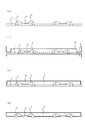
図1は本発明の第1の実施例である樹脂封止型半導体装置の一例を示す図で、(a)は封止体を透視した概略構成を示した斜視図であり、(b)は側面図、(c)は上面図である。 FIG. 1 is a diagram showing an example of a resin-encapsulated semiconductor device according to a first embodiment of the present invention, wherein (a) is a perspective view showing a schematic configuration seen through a sealing body, and (b) Side view, (c) is a top view.
本実施例で示す樹脂封止型半導体装置は、6個の外部接続端子を有する6ピンタイプの半導体装置である。図1(a)に示すとおり、半導体素子4と、内外部端子となる導電性
のマイクロボール3と、半導体素子4とマイクロボール3を電気的に接続する金属ワイヤ5と、半導体素子4、マイクロボール3の一部、および金属ワイヤ5とを絶縁樹脂7で封止する封止体とを備えている。図1(b)に示すように、半導体素子4の裏面は、封止体の底面と一平面をなすように露出し、外部端子としてマイクロボール3の少なくとも一部は、封止体の裏面から突出した露出部を有している。マイクロボール3は、封止体内の半導体素子4との内部接続用配線の役割と、実装基板との接続に用いる外部接続用端子としての役割を兼ね備えている。
The resin-encapsulated semiconductor device shown in this embodiment is a 6-pin type semiconductor device having six external connection terminals. As shown in FIG. 1A, a
次に本実施例の樹脂封止型半導体装置を具体的な寸法例を用いて説明する。ここでは、0.15mm厚にバックグラインドされた半導体素子4を用い、マイクロボール3の搭載ピッチLを0.5mm、マイクロボール3の直径を0.25mmにした。ここで使用するマイクロボールは、プラスチック粒子表面にニッケル次いで金メッキを施したボールを使用する(参考:積水化学、ミクロパール(登録商標))。半導体素子4とマイクロボール3を電気的に接続する金属ワイヤ5は20μm径の金線を使用した。本実施例では、半導体素子4の上面部の高さが、マイクロボール3の上面部よりも低くなる、打ち上げのワイヤリング構成としている。ただし、要求されるディメンション、金属ワイヤ5のループ高さの制約条件によっては、半導体素子4の上面部の高さを、マイクロボール3の上面部よりも高い構造として、半導体素子4からマイクロボール3へ打ち下げのワイヤリング形態としても良い。マイクロボール3に接続するセカンドボンディングの接続点を、マイクロボール3の上面部の頂点にすると、ボンディングの押し付け力が安定し、より一層、接続信頼性を確保することができる。本実施例で示した樹脂封止型半導体装置の外形寸法は、1.6mm×1.4mm、厚さ0.4mm、スタンドオフ0.05mmの構成となる。
Next, the resin-encapsulated semiconductor device of this example will be described using specific example dimensions. Here, the
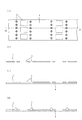
図3は本発明の第1実施例で樹脂封止型半導体装置の製造方法を工程ごとに示した図である。
初めに図3(a)に示されるようにステンレス、銅などの導電性金属薄板1あるいは耐熱ゴム薄板または樹脂薄板を用いる。例えば本実施例の場合は、1.0mm厚のステンレス薄板にレーザー加工により円柱形の開口部2を形成した薄板1を準備する。開口部にはテーパを施し面取り加工を施す。ここで図3(a)は上面図、図3(b)は図3(a)のx1−x1断面図である。
FIG. 3 is a diagram showing a method of manufacturing a resin-encapsulated semiconductor device for each step in the first embodiment of the present invention.
First, as shown in FIG. 3A, a conductive metal
次いで、図3(c)に示すとおりに薄板1の開口部2にマイクロボール3をボールマウント法により搭載する。ボール搭載の方法は、開口部分を吸着しながらスキージを滑らせて搭載する、または薄板を振動させながらボールを吸着搭載する、どちらの方法を使用しても良い。ここで使用するマイクロボール3の材質はプラスチックの粒子表面を金、銀、アルミ、ニッケルなどの金属メッキが施されたボールで本メッキは単一組成のメッキもしくは多層組成のメッキで形成させる。例えば、本実施例ではプラスチック粒子表面にニッケル次いで金メッキを施したボールを使用する(参考:積水化学、ミクロパール(登録商標))。また、マイクロボール3は金、銀、アルミ、ニッケルなどの金属ボールを用いても良い。前記のボールは単一材料もしくは多種の材料で積層形成されたものでもよい。マイクロボール3は直径25μm〜500μmの大きさのものを用いる。
Next, as shown in FIG. 3C, the
次いで図3(d)に示されるとおり半導体素子4を接着材により薄板1に固定する。半導体素子4を薄板1に固定する際にはマイクロボール3は薄板1の開口部2に吸引固定した状態、または、搭載されたすべてのマイクロボール3の上面をプレスしてあらかじめ開口部に押込み固定された状態、または、接着材で固定した状態で行う。
Next, as shown in FIG. 3D, the
次いで図4(e)に示されるとおり半導体素子4の電極とマイクロボール3とを電気的に接続する。接続は金、銅もしくはアルミワイヤを用いたワイヤボンディング法によって行われ、マイクロボール3は前項のとおり薄板1に固定された状態で行われる。
Next, as shown in FIG. 4E, the electrode of the
次いで絶縁樹脂7を用いて半導体素子4を封止する。図4(f)に示されるとおり封止の際は前項のとおりマイクロボール3が薄板1に固定された状態で行われ、ここではエポキシ樹脂を用いたトランスファモールド法により行う。樹脂を封止する際はポッティング法を用いても良い。実施例1の樹脂封止型半導体装置は図4(g)に示されるとおり絶縁樹脂7内にマイクロボール3がボールの下端面を除いて埋め込まれる形態をとる。
Next, the
次いで樹脂のキュア処理後、図4(h)に示されるとおり薄板1を封止体から除去して半導体素子4および外部接続用電極となるマイクロボール3の下端面を露出させる。薄板1の除去方法は物理的な引き剥がし、または、バックグラインド装置などを使用した研削、研磨、またはウエットエッチングによって行なう。
Next, after the resin is cured, as shown in FIG. 4H, the
次いで図5(i)の樹脂封止体断面図、図5(j)の樹脂封止体上面図に示されるy2−y2部をダイシング法で各々の半導体装置に個片化する。図6は、実施例1の樹脂封止型半導体装置の最終形態を示す断面図である。 Next, the y2-y2 portion shown in the cross-sectional view of the resin sealing body in FIG. 5 (i) and the top view of the resin sealing body in FIG. 5 (j) is separated into individual semiconductor devices by a dicing method. FIG. 6 is a cross-sectional view showing the final form of the resin-encapsulated semiconductor device of Example 1.
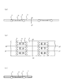
図2は、本発明の第2の実施例となる樹脂封止型半導体装置の構造を説明する図であり、(a)は封止体を透視した概略構成を示した斜視図であり、(b)は側面図、(c)下面図である。 FIG. 2 is a diagram for explaining the structure of a resin-encapsulated semiconductor device according to a second embodiment of the present invention. FIG. 2A is a perspective view showing a schematic configuration seen through a sealing body. b) is a side view, and (c) is a bottom view.
本実施例で示す樹脂封止型半導体装置は、6個の外部接続端子を有する6ピンタイプの半導体装置である。図2(a)に示すとおり、半導体素子4と、内外部端子となる導電性のマイクロボール3と、半導体素子4とマイクロボール3を電気的に接続する金属ワイヤ5と、半導体素子4、マイクロボール3の一部、および金属ワイヤ5とを絶縁樹脂7で封止する封止体とを備えている。図2(b)に示すように、半導体素子4の裏面と外部端子としてマイクロボール3の少なくとも一部は、封止体の底面と一平面をなすように露出している。マイクロボール3は、封止体内の半導体素子4との内部接続用配線の役割と、実装基板との接続に用いる外部接続用端子としての役割を兼ね備えている。
The resin-encapsulated semiconductor device shown in this embodiment is a 6-pin type semiconductor device having six external connection terminals. As shown in FIG. 2A, the
次に本実施例の樹脂封止型半導体装置を具体的な寸法例を用いて説明する。ここでは、0.15mm厚にバックグラインドされた半導体素子4を用い、マイクロボール3の搭載ピッチLを0.5mm、マイクロボール3の直径を0.25mmにした。ここで使用するマイクロボールは、プラスチック粒子表面にニッケル次いで金メッキを施したボールを使用する(参考:積水化学、ミクロパール(登録商標))。半導体素子4とマイクロボール3を電気的に接続する金属ワイヤ5は20μm径の金線を使用した。本実施例では、半導体素子4の上面部の高さが、マイクロボール3の上面部よりも低くなる打ち上げのワイヤリング構成としている。ただし、要求されるディメンション、金属ワイヤ5のループ高さの制約条件によっては、半導体素子4の上面部の高さを、マイクロボール3の上面部よりも高い構造として、半導体素子4からマイクロボール3へ打ち下げのワイヤリング形態としても良い。マイクロボール3に接続するセカンドボンディングの接続点を、マイクロボール3の上面部の頂点にすると、ボンディングの押し付け力が安定し、より一層、接続信頼性を確保することができる。本実施例で示した樹脂封止型半導体装置の外形寸法は、1.6mm×1.4mm、厚さ0.4mm、スタンドオフ0.05mmの構成となる。
Next, the resin-encapsulated semiconductor device of this example will be described using specific example dimensions. Here, the
実施例2の樹脂封止型半導体装置は実施例1の樹脂封止型半導体装置の製造方法と樹脂封止前まで同一プロセスで行われる。 The resin-encapsulated semiconductor device of Example 2 is performed in the same process as the method for manufacturing the resin-encapsulated semiconductor device of Example 1 before resin encapsulation.
実施例2の樹脂封止型半導体装置は、実施例1と同様、図7(a)に示されるとおり絶縁樹脂7を用いて半導体素子4を封止する。図7(a)に示されるとおり、マイクロボール3
の上端面が樹脂封止金型(上型)と接触し、マイクロボールに押付け圧力が負荷された状態で絶縁樹脂7を薄板1上に片面封止することにより形成する。ここでは、エポキシ樹脂を用いたトランスファモールド法により行う。実施例2の樹脂封止型半導体装置は図7(b)に示されるとおり樹脂封止金型に接触したマイクロボール3の上端面が露出する形態となる。
As in the first embodiment, the resin-encapsulated semiconductor device in the second embodiment seals the
Is formed by sealing the insulating
次いで、図7(c)に示されるとおり実施例1と同様に樹脂のキュア処理後、薄板1を封止体から除去して半導体素子4および外部接続用電極となるマイクロボール3の下端面を露出させる。薄板1の除去方法は物理的な引き剥がし、または、バックグラインド装置などを使用した研削、研磨、またはウエットエッチングによって行なう。実施例2の樹脂封止型半導体装置は半導体装置の上下面に外部接続端子が露出する。
Next, as shown in FIG. 7C, after the resin curing treatment as in Example 1, the
次いで図8(d)の樹脂封止体断面図、図8(e)の樹脂封止体上面図に示されるy2−y2部をダイシング法で各々の半導体装置に個片化する。図8(f)は、実施例2の半導体装置の最終形態(断面図)を示す。 Next, the y2-y2 portion shown in the cross-sectional view of the resin sealing body in FIG. 8D and the top view of the resin sealing body in FIG. 8E is separated into individual semiconductor devices by a dicing method. FIG. 8F shows the final form (cross-sectional view) of the semiconductor device of Example 2.
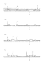
図9は本発明の第3実施例で樹脂封止型半導体装置の製造方法を工程ごとに示した図である。
初めに図9(a)に示されるようにステンレス、銅などの導電性金属薄板1あるいは耐熱ゴム、樹脂薄板を用い、例えば本実施例の場合は、0.08mm厚の銅薄板にパンチを用いたプレス加工により円柱形の開口部2を形成する。開口部にはテーパを施し面取り加工を施してもよい。図9(a)は上面図、図9(b)〜図9(j)は、図9(a)のx2−x2で示される位置における工程順の断面図である。
FIG. 9 is a diagram showing a method of manufacturing a resin-encapsulated semiconductor device for each step in the third embodiment of the present invention.
First, as shown in FIG. 9A, a conductive metal
次いで、図9(c)に示すとおりに薄板1のテーパを形成した面と反対側の面にUVテープ8を貼り付ける。
Next, as shown in FIG. 9C, the
次いで、図9(d)に示すとおり、薄板1を振動させること、もしくは、スキージを滑らせることでマイクロボール3を開口部2に搭載する。ここで使用するマイクロボール3の材質はプラスチックの粒子表面を金、銀、アルミ、ニッケルなどの金属メッキが施されたボールを用いる。本メッキは単一組成のメッキもしくは多層組成のメッキで形成する。例えば、本実施例ではプラスチック粒子表面にニッケル次いで金メッキを施したボールを使用する(参考:積水化学、ミクロパール(登録商標))。プラスチック粒子の代わりに銅、ニッケルなどの金属粒子をコアに用いて、金、銀、アルミ、ニッケル、パラジウムなどの単一組成もしくは多層のメッキをした金属ボールを用いることもできる。マイクロボール3は、直径25μm〜500μmの大きさのものを用いる。
Next, as shown in FIG. 9D, the
次いで図10(e)に示されるとおり、マイクロボール3の上面部をローラー9でプレスして、図10(f)に示すとおり、テープの接着部内にマイクロボール3を固定する。
Next, as shown in FIG. 10 (e), the upper surface portion of the
次いで図10(g)に示されるとおり、半導体素子4を薄板1上に接着材(図示なし)を介して接続する。
Next, as shown in FIG. 10G, the
次いで図10(h)に示されるとおり電極とマイクロボール3とを電気的に接続する。接続は金、銅もしくはアルミワイヤを用いたワイヤボンディング法によって行われ、マイクロボール3は前項のとおり薄板1にテープ8を介して固定された状態で行われる。ここでは、20μmの金線を用いた。
Next, as shown in FIG. 10H, the electrode and the
次いで絶縁樹脂7を用いて半導体素子4を封止する。図11(i)に示されるとおり封止
の際は前項のとおりマイクロボール3がテープ8を介して薄板1に固定された状態で行われ、ここでは、トランスファモールド法により、樹脂封止金型6内に絶縁樹脂7を注入する。絶縁樹脂を封止する際には、トランスファモールド法の代わりに、ポッティング法を用いても良い。実施例3の樹脂封止型半導体装置は図11(j)に示されるとおり絶縁樹脂7内にマイクロボール3がボールの下端面を除いて埋め込まれる形態となる。
Next, the
次いで、樹脂をキュア処理後、図11(k)に示されるとおり薄板1およびテープ8を封止体から除去して半導体素子4および外部接続用電極となるマイクロボール3の下端面を露出させる。薄板1の除去方法は物理的な引き剥がし、または、バックグラインド装置などを使用した研削、研磨、またはウエットエッチングによって行なう。
Next, after the resin is cured, as shown in FIG. 11 (k), the
次いで図12(l)の樹脂封止体断面図および図12(m)の樹脂封止体上面図に示されるy2−y2部をダイシング法で各々の半導体装置に個片化する。図12(n)は、第3実施例の樹脂封止型半導体装置の最終形態(断面図)を示す。 Next, the y2-y2 portion shown in the cross-sectional view of the resin sealing body in FIG. 12 (l) and the top view of the resin sealing body in FIG. 12 (m) is separated into individual semiconductor devices by a dicing method. FIG. 12 (n) shows the final form (cross-sectional view) of the resin-encapsulated semiconductor device of the third embodiment.
図13は本発明の第4の実施例で樹脂封止型半導体装置の製造方法を工程ごとに示した図である。 FIG. 13 is a diagram showing a method of manufacturing a resin-encapsulated semiconductor device for each step in the fourth embodiment of the present invention.
初めに図13(a)に示されるようにステンレス、銅などの導電性金属薄板1あるいは耐熱ゴム、樹脂薄板を用い、例えば本実施例の場合は、0.08mm厚の銅薄板にパンチを用いたプレス加工により円柱形および四角形の開口部2を形成する。開口部にはテーパを施し面取り加工を施してもよい。図13(a)は上面図、図13(b)〜図13(k)は、図13(a)のx2−x2の位置における工程順の断面図である。
First, as shown in FIG. 13A, a conductive metal
次いで、図13(c)に示すとおりに薄板1のテーパを形成した面と反対側の面にUVテープ8を貼り付ける。
Next, as shown in FIG. 13C, the
次いで、図13(d)に示すとおり、ボールマウント法によってマイクロボール3を円柱形の開口部2に搭載する。ここで使用するマイクロボール3の材質はプラスチックの粒子表面を金、銀、アルミ、ニッケルなどの金属メッキが施されたボールを用いる。本メッキは単一組成のメッキもしくは多層組成のメッキで形成する。例えば、本実施例ではプラスチック粒子表面にニッケル次いで金メッキを施したボールを使用する(参考:積水化学、ミクロパール(登録商標))。プラスチック粒子の代わりに銅、ニッケルなどの金属粒子をコアに用いて、金、銀、アルミ、ニッケル、パラジウムなどの単一組成もしくは多層のメッキをした金属ボールを用いることもできる。マイクロボール3は、直径25μm〜500μmの大きさのものを用いる。
Next, as shown in FIG. 13D, the
次いで図14(e)に示されるとおり、マイクロボール3の上面部をローラー9でプレスして、図14(f)に示すとおり、テープの接着部内にマイクロボール3を固定する。
Next, as shown in FIG. 14 (e), the upper surface portion of the
次いで図14(g)に示されるとおり、半導体素子4を四角形の開口部2を介してテープ8によって接続する。
Next, as shown in FIG. 14G, the
次いで図14(h)に示されるとおり電極とマイクロボール3とを電気的に接続する。接続は金、銅もしくはアルミワイヤを用いたワイヤボンディング法によって行われ、マイクロボール3は前項のとおり薄板1にテープ8を介して固定された状態で行われる。ここでは、20μmの金線を用いた。
Next, as shown in FIG. 14H, the electrode and the
次いで絶縁樹脂7を用いて半導体素子4を封止する。図15(i)に示されるとおり封止
の際は前項のとおりマイクロボール3がテープ8を介して薄板1に固定された状態で行われ、ここでは、トランスファモールド法により、樹脂封止金型6内に絶縁樹脂7を注入する。絶縁樹脂を封止する際には、トランスファモールド法の代わりに、ポッティング法を用いても良い。実施例4の樹脂封止型半導体装置は図15(j)に示されるとおり絶縁樹脂7内にマイクロボール3がボールの下端面を除いて埋め込まれる形態となる。
Next, the
次いで樹脂のキュア処理後、図15(k)に示されるとおり薄板1およびテープ8を封止体から除去して半導体素子4および外部接続用電極となるマイクロボール3の下端面を露出させる。薄板1の除去方法は物理的な引き剥がし、または、バックグラインド装置などを使用した研削、研磨、またはウエットエッチングによって行なう。
Next, after the resin is cured, as shown in FIG. 15 (k), the
次いで図16(l)の樹脂封止体断面図および図16(m)の樹脂封止体上面図に示されるy2−y2部をダイシング法で各々の半導体装置に個片化する。図16(n)は、第4の実施例の樹脂封止型半導体装置の最終形態(断面図)を示す。 Next, the y2-y2 portion shown in the cross-sectional view of the resin sealing body in FIG. 16L and the top view of the resin sealing body in FIG. 16M is separated into individual semiconductor devices by a dicing method. FIG. 16 (n) shows the final form (cross-sectional view) of the resin-encapsulated semiconductor device of the fourth embodiment.
1 薄板
2 開口部
3 マイクロボール
4 半導体素子
5 金属ワイヤ
6 樹脂封止金型
7 絶縁樹脂
8 テープ
9 ローラー
DESCRIPTION OF
Claims (7)
前記マイクロボールがプラスチックの粒子表面に金属メッキを施したボールであり、前記金属メッキは単一組成のメッキもしくは多層組成のメッキにより形成され、前記半導体素子の裏面が前記封止体から露出し、かつ、前記複数のマイクロボールの一部が前記外部端子面として前記封止体の底面から突起状に露出していることを特徴とする樹脂封止型半導体装置。 A semiconductor element, a plurality of microballs having an internal terminal surface and an external terminal surface integrated with each other, a metal wire that electrically connects the semiconductor element and the internal terminal surface, the semiconductor element, and the plurality of microballs In a resin-encapsulated semiconductor device provided with a part of and a sealing body that seals the wire with a sealing resin,
The microball is a ball obtained by performing metal plating on a plastic particle surface, and the metal plating is formed by single composition plating or multilayer composition plating, and the back surface of the semiconductor element is exposed from the sealing body, and, wherein the plurality of micro part the sealing body resin-sealed semiconductor device characterized by being exposed protruding from the bottom surface as the external terminal face of the ball.
前記半導体素子の周囲に配置された複数のマイクロボールと、
前記半導体素子と、前記複数のマイクロボールのそれぞれの第1の部分である内部端子面とを電気的に接続する金属ワイヤと、
前記半導体素子、前記複数のマイクロボールのそれぞれの所望の領域、および、前記ワイヤを封止樹脂で封止する封止体とからなり、
前記マイクロボールがプラスチックの粒子表面に金属メッキを施したボールであり、前記金属メッキは単一組成のメッキもしくは多層組成のメッキにより形成され、
前記半導体素子の裏面が前記封止体から露出し、前記複数のマイクロボールのそれぞれの第2の部分が外部端子面として前記封止体の底面から突起状に露出している樹脂封止型半導体装置。 A semiconductor element, and a plurality of microballs disposed around the semiconductor element;
A metal wire that electrically connects the semiconductor element and an internal terminal surface that is a first portion of each of the plurality of microballs;
The semiconductor element, each desired region of the plurality of microballs, and a sealing body that seals the wire with a sealing resin,
The microball is a ball obtained by metal plating on a plastic particle surface, and the metal plating is formed by single composition plating or multilayer composition plating,
The back surface of the semiconductor element is exposed from the sealing body, wherein the plurality of each of the second part the sealing body molding semiconductor exposed in the protruding from the bottom surface of the external terminal face of the microballs apparatus.
Priority Applications (6)
| Application Number | Priority Date | Filing Date | Title |
|---|---|---|---|
| JP2009258415A JP5588150B2 (en) | 2009-02-06 | 2009-11-11 | Resin-sealed semiconductor device |
| TW099101642A TWI478296B (en) | 2009-02-06 | 2010-01-21 | Semiconductor device |
| US12/701,018 US8703532B2 (en) | 2009-02-06 | 2010-02-05 | Semiconductor device and manufacturing method thereof |
| CN201010113656.6A CN101901788B (en) | 2009-02-06 | 2010-02-05 | Resin sealing type semiconductor device, and manufacturing method thereof |
| KR1020100011105A KR101665963B1 (en) | 2009-02-06 | 2010-02-05 | Semiconductor device and manufacturing method thereof |
| US14/150,153 US9490224B2 (en) | 2009-02-06 | 2014-01-08 | Semiconductor device and manufacturing method thereof |
Applications Claiming Priority (3)
| Application Number | Priority Date | Filing Date | Title |
|---|---|---|---|
| JP2009026507 | 2009-02-06 | ||
| JP2009026507 | 2009-02-06 | ||
| JP2009258415A JP5588150B2 (en) | 2009-02-06 | 2009-11-11 | Resin-sealed semiconductor device |
Publications (3)
| Publication Number | Publication Date |
|---|---|
| JP2010206162A JP2010206162A (en) | 2010-09-16 |
| JP2010206162A5 JP2010206162A5 (en) | 2012-10-25 |
| JP5588150B2 true JP5588150B2 (en) | 2014-09-10 |
Family
ID=42539745
Family Applications (1)
| Application Number | Title | Priority Date | Filing Date |
|---|---|---|---|
| JP2009258415A Expired - Fee Related JP5588150B2 (en) | 2009-02-06 | 2009-11-11 | Resin-sealed semiconductor device |
Country Status (5)
| Country | Link |
|---|---|
| US (2) | US8703532B2 (en) |
| JP (1) | JP5588150B2 (en) |
| KR (1) | KR101665963B1 (en) |
| CN (1) | CN101901788B (en) |
| TW (1) | TWI478296B (en) |
Families Citing this family (8)
| Publication number | Priority date | Publication date | Assignee | Title |
|---|---|---|---|---|
| JP5642473B2 (en) * | 2010-09-22 | 2014-12-17 | セイコーインスツル株式会社 | BGA semiconductor package and manufacturing method thereof |
| CN102786028B (en) * | 2012-07-17 | 2015-05-06 | 西南交通大学 | Manufacturing method of multi-needle point array used for large area friction induced micro/nano-processing |
| CN102832141A (en) * | 2012-08-18 | 2012-12-19 | 孙青秀 | Manufacturing process of carrier-free package based on framework |
| US9711479B2 (en) | 2013-07-03 | 2017-07-18 | Rosenberger Hochfrequenztechnik Gmbh & Co. Kg | Substrate less die package having wires with dielectric and metal coatings and the method of manufacturing the same |
| DE102015212177A1 (en) * | 2015-06-30 | 2017-01-05 | Osram Gmbh | Circuit carrier for an electronic circuit and method for producing such a circuit carrier |
| CN105489509A (en) * | 2015-12-25 | 2016-04-13 | 华天科技(西安)有限公司 | Optical sensing chip package method for optimizing coating process by applying metal stencil printing technology |
| CN110517963A (en) * | 2019-09-05 | 2019-11-29 | 合肥矽迈微电子科技有限公司 | A kind of ring membrane structure Shooting Technique |
| US20220227104A1 (en) * | 2019-09-13 | 2022-07-21 | Showa Denko K.K. | Laminate and method for producing same |
Family Cites Families (19)
| Publication number | Priority date | Publication date | Assignee | Title |
|---|---|---|---|---|
| JP3129169B2 (en) * | 1995-11-08 | 2001-01-29 | 富士通株式会社 | Semiconductor device and manufacturing method thereof |
| KR100332378B1 (en) * | 1999-09-11 | 2002-04-12 | 이병구 | Fluxless soldering method |
| JP3823651B2 (en) * | 2000-01-05 | 2006-09-20 | 松下電器産業株式会社 | Manufacturing method of resin-encapsulated semiconductor device |
| JP2001230270A (en) * | 2000-02-14 | 2001-08-24 | Fujitsu Ltd | Semiconductor device and its manufacturing method |
| JP3626075B2 (en) | 2000-06-20 | 2005-03-02 | 九州日立マクセル株式会社 | Manufacturing method of semiconductor device |
| US20020033527A1 (en) * | 2000-09-19 | 2002-03-21 | Siliconware Precision Industries Co., Ltd. | Semiconductor device and manufacturing process thereof |
| US7297572B2 (en) * | 2001-09-07 | 2007-11-20 | Hynix Semiconductor, Inc. | Fabrication method for electronic system modules |
| JP4014912B2 (en) * | 2001-09-28 | 2007-11-28 | 株式会社ルネサステクノロジ | Semiconductor device |
| CN1477703A (en) * | 2002-08-02 | 2004-02-25 | 千住金属工业株式会社 | Soldering ball assembly and producing method, method for forming welding block |
| JP2004319577A (en) * | 2003-04-11 | 2004-11-11 | Dainippon Printing Co Ltd | Resin sealed semiconductor device, its manufacturing process, and stacked resin sealed semiconductor device |
| US7056766B2 (en) * | 2003-12-09 | 2006-06-06 | Freescale Semiconductor, Inc. | Method of forming land grid array packaged device |
| JP2005194393A (en) * | 2004-01-07 | 2005-07-21 | Hitachi Chem Co Ltd | Adhesive film for circuit connection, and circuit connection structure |
| KR20050079399A (en) * | 2004-02-05 | 2005-08-10 | 삼성전자주식회사 | Anisotropic conductive film and bump, and packaging structure of semiconductor having the same |
| US7205178B2 (en) * | 2004-03-24 | 2007-04-17 | Freescale Semiconductor, Inc. | Land grid array packaged device and method of forming same |
| JP2006066521A (en) * | 2004-08-25 | 2006-03-09 | Fujitsu Ltd | Semiconductor device and method of manufacturing the same |
| US8169067B2 (en) * | 2006-10-20 | 2012-05-01 | Broadcom Corporation | Low profile ball grid array (BGA) package with exposed die and method of making same |
| KR100792663B1 (en) * | 2006-12-01 | 2008-01-09 | 주식회사 동부하이텍 | Preparation method of plastic conductive particles having multi-coating layer for electronic package and plastic conductive particles manufactured thereby |
| US20080308935A1 (en) * | 2007-06-18 | 2008-12-18 | Samsung Electronics Co., Ltd. | Semiconductor chip package, semiconductor package including semiconductor chip package, and method of fabricating semiconductor package |
| US8501088B2 (en) * | 2007-07-25 | 2013-08-06 | Nippon Steel & Sumikin Materials Co., Ltd. | Solder alloy, solder ball and electronic member having solder bump |
-
2009
- 2009-11-11 JP JP2009258415A patent/JP5588150B2/en not_active Expired - Fee Related
-
2010
- 2010-01-21 TW TW099101642A patent/TWI478296B/en not_active IP Right Cessation
- 2010-02-05 KR KR1020100011105A patent/KR101665963B1/en active IP Right Grant
- 2010-02-05 US US12/701,018 patent/US8703532B2/en not_active Expired - Fee Related
- 2010-02-05 CN CN201010113656.6A patent/CN101901788B/en not_active Expired - Fee Related
-
2014
- 2014-01-08 US US14/150,153 patent/US9490224B2/en active Active
Also Published As
| Publication number | Publication date |
|---|---|
| US20100200982A1 (en) | 2010-08-12 |
| US20140117544A1 (en) | 2014-05-01 |
| CN101901788B (en) | 2014-10-29 |
| US8703532B2 (en) | 2014-04-22 |
| TW201036118A (en) | 2010-10-01 |
| JP2010206162A (en) | 2010-09-16 |
| TWI478296B (en) | 2015-03-21 |
| KR101665963B1 (en) | 2016-10-24 |
| US9490224B2 (en) | 2016-11-08 |
| CN101901788A (en) | 2010-12-01 |
| KR20100090666A (en) | 2010-08-16 |
Similar Documents
| Publication | Publication Date | Title |
|---|---|---|
| JP5588150B2 (en) | Resin-sealed semiconductor device | |
| US6909178B2 (en) | Semiconductor device and method of manufacturing the same | |
| US20080023819A1 (en) | Package structure having semiconductor chip embedded therein and method for fabricating the same | |
| US8211754B2 (en) | Semiconductor device and manufacturing method thereof | |
| KR20080049760A (en) | Semiconductor device and method for manufacturing same | |
| JP2013069807A (en) | Semiconductor package and method for manufacturing the same | |
| US9245864B2 (en) | Ball grid array semiconductor package and method of manufacturing the same | |
| JP2021027116A (en) | Semiconductor device | |
| TW201631715A (en) | Wiring substrate, method of manufacturing the same and electronic component device | |
| JP6964477B2 (en) | Substrate for semiconductor device and its manufacturing method, semiconductor device and its manufacturing method | |
| JP4379693B2 (en) | Semiconductor device and manufacturing method thereof | |
| JP4970388B2 (en) | Semiconductor device and manufacturing method of semiconductor device | |
| WO2007057954A1 (en) | Semiconductor device and method for manufacturing same | |
| JP3925503B2 (en) | Semiconductor device | |
| KR20040030301A (en) | Method of manufacturing circuit device | |
| JP2956659B2 (en) | Semiconductor device and its lead frame | |
| JP4577316B2 (en) | Manufacturing method of semiconductor device | |
| JP4979661B2 (en) | Manufacturing method of semiconductor device | |
| JP4089629B2 (en) | Optical sensor module | |
| JP4321758B2 (en) | Semiconductor device | |
| JP2003046053A (en) | Semiconductor device and manufacturing method therefor | |
| JP2005116886A (en) | Manufacturing method of semiconductor device | |
| JPH0738015A (en) | Resin-sealed semiconductor device and manufacture thereof | |
| JP2009302427A (en) | Semiconductor device, and method of manufacturing the same | |
| JP2005044931A (en) | Semiconductor mounting substrate, method of manufacturing the same, semiconductor package and method of manufacturing the same |
Legal Events
| Date | Code | Title | Description |
|---|---|---|---|
| A521 | Request for written amendment filed |
Free format text: JAPANESE INTERMEDIATE CODE: A523 Effective date: 20120911 |
|
| A621 | Written request for application examination |
Free format text: JAPANESE INTERMEDIATE CODE: A621 Effective date: 20120911 |
|
| A977 | Report on retrieval |
Free format text: JAPANESE INTERMEDIATE CODE: A971007 Effective date: 20130513 |
|
| A131 | Notification of reasons for refusal |
Free format text: JAPANESE INTERMEDIATE CODE: A131 Effective date: 20130521 |
|
| A521 | Request for written amendment filed |
Free format text: JAPANESE INTERMEDIATE CODE: A523 Effective date: 20130718 |
|
| A131 | Notification of reasons for refusal |
Free format text: JAPANESE INTERMEDIATE CODE: A131 Effective date: 20140415 |
|
| A521 | Request for written amendment filed |
Free format text: JAPANESE INTERMEDIATE CODE: A523 Effective date: 20140612 |
|
| TRDD | Decision of grant or rejection written | ||
| A01 | Written decision to grant a patent or to grant a registration (utility model) |
Free format text: JAPANESE INTERMEDIATE CODE: A01 Effective date: 20140701 |
|
| A61 | First payment of annual fees (during grant procedure) |
Free format text: JAPANESE INTERMEDIATE CODE: A61 Effective date: 20140725 |
|
| R150 | Certificate of patent or registration of utility model |
Ref document number: 5588150 Country of ref document: JP Free format text: JAPANESE INTERMEDIATE CODE: R150 |
|
| S111 | Request for change of ownership or part of ownership |
Free format text: JAPANESE INTERMEDIATE CODE: R313113 |
|
| R350 | Written notification of registration of transfer |
Free format text: JAPANESE INTERMEDIATE CODE: R350 |
|
| R250 | Receipt of annual fees |
Free format text: JAPANESE INTERMEDIATE CODE: R250 |
|
| S533 | Written request for registration of change of name |
Free format text: JAPANESE INTERMEDIATE CODE: R313533 |
|
| R350 | Written notification of registration of transfer |
Free format text: JAPANESE INTERMEDIATE CODE: R350 |
|
| R250 | Receipt of annual fees |
Free format text: JAPANESE INTERMEDIATE CODE: R250 |
|
| R250 | Receipt of annual fees |
Free format text: JAPANESE INTERMEDIATE CODE: R250 |
|
| R250 | Receipt of annual fees |
Free format text: JAPANESE INTERMEDIATE CODE: R250 |
|
| LAPS | Cancellation because of no payment of annual fees |