JP2013069807A - Semiconductor package and method for manufacturing the same - Google Patents
Semiconductor package and method for manufacturing the same Download PDFInfo
- Publication number
- JP2013069807A JP2013069807A JP2011206549A JP2011206549A JP2013069807A JP 2013069807 A JP2013069807 A JP 2013069807A JP 2011206549 A JP2011206549 A JP 2011206549A JP 2011206549 A JP2011206549 A JP 2011206549A JP 2013069807 A JP2013069807 A JP 2013069807A
- Authority
- JP
- Japan
- Prior art keywords
- insulating layer
- semiconductor chip
- layer
- wiring
- semiconductor
- Prior art date
- Legal status (The legal status is an assumption and is not a legal conclusion. Google has not performed a legal analysis and makes no representation as to the accuracy of the status listed.)
- Pending
Links
Images


Classifications
-
- H—ELECTRICITY
- H01—ELECTRIC ELEMENTS
- H01L—SEMICONDUCTOR DEVICES NOT COVERED BY CLASS H10
- H01L23/00—Details of semiconductor or other solid state devices
- H01L23/52—Arrangements for conducting electric current within the device in operation from one component to another, i.e. interconnections, e.g. wires, lead frames
- H01L23/538—Arrangements for conducting electric current within the device in operation from one component to another, i.e. interconnections, e.g. wires, lead frames the interconnection structure between a plurality of semiconductor chips being formed on, or in, insulating substrates
- H01L23/5389—Arrangements for conducting electric current within the device in operation from one component to another, i.e. interconnections, e.g. wires, lead frames the interconnection structure between a plurality of semiconductor chips being formed on, or in, insulating substrates the chips being integrally enclosed by the interconnect and support structures
-
- H—ELECTRICITY
- H01—ELECTRIC ELEMENTS
- H01L—SEMICONDUCTOR DEVICES NOT COVERED BY CLASS H10
- H01L21/00—Processes or apparatus adapted for the manufacture or treatment of semiconductor or solid state devices or of parts thereof
- H01L21/02—Manufacture or treatment of semiconductor devices or of parts thereof
- H01L21/04—Manufacture or treatment of semiconductor devices or of parts thereof the devices having at least one potential-jump barrier or surface barrier, e.g. PN junction, depletion layer or carrier concentration layer
- H01L21/48—Manufacture or treatment of parts, e.g. containers, prior to assembly of the devices, using processes not provided for in a single one of the subgroups H01L21/06 - H01L21/326
- H01L21/4814—Conductive parts
- H01L21/4846—Leads on or in insulating or insulated substrates, e.g. metallisation
- H01L21/4857—Multilayer substrates
-
- H—ELECTRICITY
- H01—ELECTRIC ELEMENTS
- H01L—SEMICONDUCTOR DEVICES NOT COVERED BY CLASS H10
- H01L21/00—Processes or apparatus adapted for the manufacture or treatment of semiconductor or solid state devices or of parts thereof
- H01L21/02—Manufacture or treatment of semiconductor devices or of parts thereof
- H01L21/04—Manufacture or treatment of semiconductor devices or of parts thereof the devices having at least one potential-jump barrier or surface barrier, e.g. PN junction, depletion layer or carrier concentration layer
- H01L21/50—Assembly of semiconductor devices using processes or apparatus not provided for in a single one of the subgroups H01L21/06 - H01L21/326, e.g. sealing of a cap to a base of a container
- H01L21/56—Encapsulations, e.g. encapsulation layers, coatings
- H01L21/568—Temporary substrate used as encapsulation process aid
-
- H—ELECTRICITY
- H01—ELECTRIC ELEMENTS
- H01L—SEMICONDUCTOR DEVICES NOT COVERED BY CLASS H10
- H01L21/00—Processes or apparatus adapted for the manufacture or treatment of semiconductor or solid state devices or of parts thereof
- H01L21/67—Apparatus specially adapted for handling semiconductor or electric solid state devices during manufacture or treatment thereof; Apparatus specially adapted for handling wafers during manufacture or treatment of semiconductor or electric solid state devices or components ; Apparatus not specifically provided for elsewhere
- H01L21/683—Apparatus specially adapted for handling semiconductor or electric solid state devices during manufacture or treatment thereof; Apparatus specially adapted for handling wafers during manufacture or treatment of semiconductor or electric solid state devices or components ; Apparatus not specifically provided for elsewhere for supporting or gripping
- H01L21/6835—Apparatus specially adapted for handling semiconductor or electric solid state devices during manufacture or treatment thereof; Apparatus specially adapted for handling wafers during manufacture or treatment of semiconductor or electric solid state devices or components ; Apparatus not specifically provided for elsewhere for supporting or gripping using temporarily an auxiliary support
-
- H—ELECTRICITY
- H01—ELECTRIC ELEMENTS
- H01L—SEMICONDUCTOR DEVICES NOT COVERED BY CLASS H10
- H01L23/00—Details of semiconductor or other solid state devices
- H01L23/48—Arrangements for conducting electric current to or from the solid state body in operation, e.g. leads, terminal arrangements ; Selection of materials therefor
- H01L23/488—Arrangements for conducting electric current to or from the solid state body in operation, e.g. leads, terminal arrangements ; Selection of materials therefor consisting of soldered or bonded constructions
- H01L23/498—Leads, i.e. metallisations or lead-frames on insulating substrates, e.g. chip carriers
- H01L23/49822—Multilayer substrates
-
- H—ELECTRICITY
- H01—ELECTRIC ELEMENTS
- H01L—SEMICONDUCTOR DEVICES NOT COVERED BY CLASS H10
- H01L24/00—Arrangements for connecting or disconnecting semiconductor or solid-state bodies; Methods or apparatus related thereto
- H01L24/01—Means for bonding being attached to, or being formed on, the surface to be connected, e.g. chip-to-package, die-attach, "first-level" interconnects; Manufacturing methods related thereto
- H01L24/18—High density interconnect [HDI] connectors; Manufacturing methods related thereto
- H01L24/23—Structure, shape, material or disposition of the high density interconnect connectors after the connecting process
- H01L24/24—Structure, shape, material or disposition of the high density interconnect connectors after the connecting process of an individual high density interconnect connector
-
- H—ELECTRICITY
- H01—ELECTRIC ELEMENTS
- H01L—SEMICONDUCTOR DEVICES NOT COVERED BY CLASS H10
- H01L25/00—Assemblies consisting of a plurality of individual semiconductor or other solid state devices ; Multistep manufacturing processes thereof
- H01L25/03—Assemblies consisting of a plurality of individual semiconductor or other solid state devices ; Multistep manufacturing processes thereof all the devices being of a type provided for in the same subgroup of groups H01L27/00 - H01L33/00, or in a single subclass of H10K, H10N, e.g. assemblies of rectifier diodes
- H01L25/04—Assemblies consisting of a plurality of individual semiconductor or other solid state devices ; Multistep manufacturing processes thereof all the devices being of a type provided for in the same subgroup of groups H01L27/00 - H01L33/00, or in a single subclass of H10K, H10N, e.g. assemblies of rectifier diodes the devices not having separate containers
- H01L25/065—Assemblies consisting of a plurality of individual semiconductor or other solid state devices ; Multistep manufacturing processes thereof all the devices being of a type provided for in the same subgroup of groups H01L27/00 - H01L33/00, or in a single subclass of H10K, H10N, e.g. assemblies of rectifier diodes the devices not having separate containers the devices being of a type provided for in group H01L27/00
- H01L25/0657—Stacked arrangements of devices
-
- H—ELECTRICITY
- H01—ELECTRIC ELEMENTS
- H01L—SEMICONDUCTOR DEVICES NOT COVERED BY CLASS H10
- H01L2221/00—Processes or apparatus adapted for the manufacture or treatment of semiconductor or solid state devices or of parts thereof covered by H01L21/00
- H01L2221/67—Apparatus for handling semiconductor or electric solid state devices during manufacture or treatment thereof; Apparatus for handling wafers during manufacture or treatment of semiconductor or electric solid state devices or components; Apparatus not specifically provided for elsewhere
- H01L2221/683—Apparatus for handling semiconductor or electric solid state devices during manufacture or treatment thereof; Apparatus for handling wafers during manufacture or treatment of semiconductor or electric solid state devices or components; Apparatus not specifically provided for elsewhere for supporting or gripping
- H01L2221/68304—Apparatus for handling semiconductor or electric solid state devices during manufacture or treatment thereof; Apparatus for handling wafers during manufacture or treatment of semiconductor or electric solid state devices or components; Apparatus not specifically provided for elsewhere for supporting or gripping using temporarily an auxiliary support
- H01L2221/68345—Apparatus for handling semiconductor or electric solid state devices during manufacture or treatment thereof; Apparatus for handling wafers during manufacture or treatment of semiconductor or electric solid state devices or components; Apparatus not specifically provided for elsewhere for supporting or gripping using temporarily an auxiliary support used as a support during the manufacture of self supporting substrates
-
- H—ELECTRICITY
- H01—ELECTRIC ELEMENTS
- H01L—SEMICONDUCTOR DEVICES NOT COVERED BY CLASS H10
- H01L2221/00—Processes or apparatus adapted for the manufacture or treatment of semiconductor or solid state devices or of parts thereof covered by H01L21/00
- H01L2221/67—Apparatus for handling semiconductor or electric solid state devices during manufacture or treatment thereof; Apparatus for handling wafers during manufacture or treatment of semiconductor or electric solid state devices or components; Apparatus not specifically provided for elsewhere
- H01L2221/683—Apparatus for handling semiconductor or electric solid state devices during manufacture or treatment thereof; Apparatus for handling wafers during manufacture or treatment of semiconductor or electric solid state devices or components; Apparatus not specifically provided for elsewhere for supporting or gripping
- H01L2221/68304—Apparatus for handling semiconductor or electric solid state devices during manufacture or treatment thereof; Apparatus for handling wafers during manufacture or treatment of semiconductor or electric solid state devices or components; Apparatus not specifically provided for elsewhere for supporting or gripping using temporarily an auxiliary support
- H01L2221/68381—Details of chemical or physical process used for separating the auxiliary support from a device or wafer
-
- H—ELECTRICITY
- H01—ELECTRIC ELEMENTS
- H01L—SEMICONDUCTOR DEVICES NOT COVERED BY CLASS H10
- H01L2224/00—Indexing scheme for arrangements for connecting or disconnecting semiconductor or solid-state bodies and methods related thereto as covered by H01L24/00
- H01L2224/01—Means for bonding being attached to, or being formed on, the surface to be connected, e.g. chip-to-package, die-attach, "first-level" interconnects; Manufacturing methods related thereto
- H01L2224/02—Bonding areas; Manufacturing methods related thereto
- H01L2224/04—Structure, shape, material or disposition of the bonding areas prior to the connecting process
- H01L2224/0401—Bonding areas specifically adapted for bump connectors, e.g. under bump metallisation [UBM]
-
- H—ELECTRICITY
- H01—ELECTRIC ELEMENTS
- H01L—SEMICONDUCTOR DEVICES NOT COVERED BY CLASS H10
- H01L2224/00—Indexing scheme for arrangements for connecting or disconnecting semiconductor or solid-state bodies and methods related thereto as covered by H01L24/00
- H01L2224/01—Means for bonding being attached to, or being formed on, the surface to be connected, e.g. chip-to-package, die-attach, "first-level" interconnects; Manufacturing methods related thereto
- H01L2224/02—Bonding areas; Manufacturing methods related thereto
- H01L2224/04—Structure, shape, material or disposition of the bonding areas prior to the connecting process
- H01L2224/04105—Bonding areas formed on an encapsulation of the semiconductor or solid-state body, e.g. bonding areas on chip-scale packages
-
- H—ELECTRICITY
- H01—ELECTRIC ELEMENTS
- H01L—SEMICONDUCTOR DEVICES NOT COVERED BY CLASS H10
- H01L2224/00—Indexing scheme for arrangements for connecting or disconnecting semiconductor or solid-state bodies and methods related thereto as covered by H01L24/00
- H01L2224/01—Means for bonding being attached to, or being formed on, the surface to be connected, e.g. chip-to-package, die-attach, "first-level" interconnects; Manufacturing methods related thereto
- H01L2224/02—Bonding areas; Manufacturing methods related thereto
- H01L2224/04—Structure, shape, material or disposition of the bonding areas prior to the connecting process
- H01L2224/05—Structure, shape, material or disposition of the bonding areas prior to the connecting process of an individual bonding area
- H01L2224/0554—External layer
- H01L2224/0556—Disposition
- H01L2224/0557—Disposition the external layer being disposed on a via connection of the semiconductor or solid-state body
-
- H—ELECTRICITY
- H01—ELECTRIC ELEMENTS
- H01L—SEMICONDUCTOR DEVICES NOT COVERED BY CLASS H10
- H01L2224/00—Indexing scheme for arrangements for connecting or disconnecting semiconductor or solid-state bodies and methods related thereto as covered by H01L24/00
- H01L2224/01—Means for bonding being attached to, or being formed on, the surface to be connected, e.g. chip-to-package, die-attach, "first-level" interconnects; Manufacturing methods related thereto
- H01L2224/10—Bump connectors; Manufacturing methods related thereto
- H01L2224/12—Structure, shape, material or disposition of the bump connectors prior to the connecting process
- H01L2224/13—Structure, shape, material or disposition of the bump connectors prior to the connecting process of an individual bump connector
- H01L2224/13001—Core members of the bump connector
- H01L2224/13099—Material
- H01L2224/131—Material with a principal constituent of the material being a metal or a metalloid, e.g. boron [B], silicon [Si], germanium [Ge], arsenic [As], antimony [Sb], tellurium [Te] and polonium [Po], and alloys thereof
- H01L2224/13101—Material with a principal constituent of the material being a metal or a metalloid, e.g. boron [B], silicon [Si], germanium [Ge], arsenic [As], antimony [Sb], tellurium [Te] and polonium [Po], and alloys thereof the principal constituent melting at a temperature of less than 400°C
- H01L2224/13111—Tin [Sn] as principal constituent
-
- H—ELECTRICITY
- H01—ELECTRIC ELEMENTS
- H01L—SEMICONDUCTOR DEVICES NOT COVERED BY CLASS H10
- H01L2224/00—Indexing scheme for arrangements for connecting or disconnecting semiconductor or solid-state bodies and methods related thereto as covered by H01L24/00
- H01L2224/01—Means for bonding being attached to, or being formed on, the surface to be connected, e.g. chip-to-package, die-attach, "first-level" interconnects; Manufacturing methods related thereto
- H01L2224/10—Bump connectors; Manufacturing methods related thereto
- H01L2224/12—Structure, shape, material or disposition of the bump connectors prior to the connecting process
- H01L2224/13—Structure, shape, material or disposition of the bump connectors prior to the connecting process of an individual bump connector
- H01L2224/13001—Core members of the bump connector
- H01L2224/13099—Material
- H01L2224/131—Material with a principal constituent of the material being a metal or a metalloid, e.g. boron [B], silicon [Si], germanium [Ge], arsenic [As], antimony [Sb], tellurium [Te] and polonium [Po], and alloys thereof
- H01L2224/13101—Material with a principal constituent of the material being a metal or a metalloid, e.g. boron [B], silicon [Si], germanium [Ge], arsenic [As], antimony [Sb], tellurium [Te] and polonium [Po], and alloys thereof the principal constituent melting at a temperature of less than 400°C
- H01L2224/13116—Lead [Pb] as principal constituent
-
- H—ELECTRICITY
- H01—ELECTRIC ELEMENTS
- H01L—SEMICONDUCTOR DEVICES NOT COVERED BY CLASS H10
- H01L2224/00—Indexing scheme for arrangements for connecting or disconnecting semiconductor or solid-state bodies and methods related thereto as covered by H01L24/00
- H01L2224/01—Means for bonding being attached to, or being formed on, the surface to be connected, e.g. chip-to-package, die-attach, "first-level" interconnects; Manufacturing methods related thereto
- H01L2224/10—Bump connectors; Manufacturing methods related thereto
- H01L2224/15—Structure, shape, material or disposition of the bump connectors after the connecting process
- H01L2224/16—Structure, shape, material or disposition of the bump connectors after the connecting process of an individual bump connector
- H01L2224/161—Disposition
- H01L2224/16135—Disposition the bump connector connecting between different semiconductor or solid-state bodies, i.e. chip-to-chip
- H01L2224/16145—Disposition the bump connector connecting between different semiconductor or solid-state bodies, i.e. chip-to-chip the bodies being stacked
- H01L2224/16146—Disposition the bump connector connecting between different semiconductor or solid-state bodies, i.e. chip-to-chip the bodies being stacked the bump connector connecting to a via connection in the semiconductor or solid-state body
-
- H—ELECTRICITY
- H01—ELECTRIC ELEMENTS
- H01L—SEMICONDUCTOR DEVICES NOT COVERED BY CLASS H10
- H01L2224/00—Indexing scheme for arrangements for connecting or disconnecting semiconductor or solid-state bodies and methods related thereto as covered by H01L24/00
- H01L2224/01—Means for bonding being attached to, or being formed on, the surface to be connected, e.g. chip-to-package, die-attach, "first-level" interconnects; Manufacturing methods related thereto
- H01L2224/10—Bump connectors; Manufacturing methods related thereto
- H01L2224/15—Structure, shape, material or disposition of the bump connectors after the connecting process
- H01L2224/16—Structure, shape, material or disposition of the bump connectors after the connecting process of an individual bump connector
- H01L2224/161—Disposition
- H01L2224/16151—Disposition the bump connector connecting between a semiconductor or solid-state body and an item not being a semiconductor or solid-state body, e.g. chip-to-substrate, chip-to-passive
- H01L2224/16221—Disposition the bump connector connecting between a semiconductor or solid-state body and an item not being a semiconductor or solid-state body, e.g. chip-to-substrate, chip-to-passive the body and the item being stacked
- H01L2224/16225—Disposition the bump connector connecting between a semiconductor or solid-state body and an item not being a semiconductor or solid-state body, e.g. chip-to-substrate, chip-to-passive the body and the item being stacked the item being non-metallic, e.g. insulating substrate with or without metallisation
- H01L2224/16237—Disposition the bump connector connecting between a semiconductor or solid-state body and an item not being a semiconductor or solid-state body, e.g. chip-to-substrate, chip-to-passive the body and the item being stacked the item being non-metallic, e.g. insulating substrate with or without metallisation the bump connector connecting to a bonding area disposed in a recess of the surface of the item
-
- H—ELECTRICITY
- H01—ELECTRIC ELEMENTS
- H01L—SEMICONDUCTOR DEVICES NOT COVERED BY CLASS H10
- H01L2224/00—Indexing scheme for arrangements for connecting or disconnecting semiconductor or solid-state bodies and methods related thereto as covered by H01L24/00
- H01L2224/01—Means for bonding being attached to, or being formed on, the surface to be connected, e.g. chip-to-package, die-attach, "first-level" interconnects; Manufacturing methods related thereto
- H01L2224/18—High density interconnect [HDI] connectors; Manufacturing methods related thereto
- H01L2224/23—Structure, shape, material or disposition of the high density interconnect connectors after the connecting process
- H01L2224/24—Structure, shape, material or disposition of the high density interconnect connectors after the connecting process of an individual high density interconnect connector
- H01L2224/241—Disposition
- H01L2224/24151—Connecting between a semiconductor or solid-state body and an item not being a semiconductor or solid-state body, e.g. chip-to-substrate, chip-to-passive
- H01L2224/24221—Connecting between a semiconductor or solid-state body and an item not being a semiconductor or solid-state body, e.g. chip-to-substrate, chip-to-passive the body and the item being stacked
- H01L2224/24245—Connecting between a semiconductor or solid-state body and an item not being a semiconductor or solid-state body, e.g. chip-to-substrate, chip-to-passive the body and the item being stacked the item being metallic
- H01L2224/24246—Connecting between a semiconductor or solid-state body and an item not being a semiconductor or solid-state body, e.g. chip-to-substrate, chip-to-passive the body and the item being stacked the item being metallic the HDI interconnect connecting to the same level of the item at which the semiconductor or solid-state body is mounted, e.g. the item being planar
-
- H—ELECTRICITY
- H01—ELECTRIC ELEMENTS
- H01L—SEMICONDUCTOR DEVICES NOT COVERED BY CLASS H10
- H01L2224/00—Indexing scheme for arrangements for connecting or disconnecting semiconductor or solid-state bodies and methods related thereto as covered by H01L24/00
- H01L2224/01—Means for bonding being attached to, or being formed on, the surface to be connected, e.g. chip-to-package, die-attach, "first-level" interconnects; Manufacturing methods related thereto
- H01L2224/26—Layer connectors, e.g. plate connectors, solder or adhesive layers; Manufacturing methods related thereto
- H01L2224/28—Structure, shape, material or disposition of the layer connectors prior to the connecting process
- H01L2224/29—Structure, shape, material or disposition of the layer connectors prior to the connecting process of an individual layer connector
- H01L2224/29001—Core members of the layer connector
- H01L2224/29099—Material
- H01L2224/2919—Material with a principal constituent of the material being a polymer, e.g. polyester, phenolic based polymer, epoxy
-
- H—ELECTRICITY
- H01—ELECTRIC ELEMENTS
- H01L—SEMICONDUCTOR DEVICES NOT COVERED BY CLASS H10
- H01L2224/00—Indexing scheme for arrangements for connecting or disconnecting semiconductor or solid-state bodies and methods related thereto as covered by H01L24/00
- H01L2224/01—Means for bonding being attached to, or being formed on, the surface to be connected, e.g. chip-to-package, die-attach, "first-level" interconnects; Manufacturing methods related thereto
- H01L2224/26—Layer connectors, e.g. plate connectors, solder or adhesive layers; Manufacturing methods related thereto
- H01L2224/28—Structure, shape, material or disposition of the layer connectors prior to the connecting process
- H01L2224/29—Structure, shape, material or disposition of the layer connectors prior to the connecting process of an individual layer connector
- H01L2224/29001—Core members of the layer connector
- H01L2224/29099—Material
- H01L2224/29198—Material with a principal constituent of the material being a combination of two or more materials in the form of a matrix with a filler, i.e. being a hybrid material, e.g. segmented structures, foams
- H01L2224/29199—Material of the matrix
- H01L2224/2929—Material of the matrix with a principal constituent of the material being a polymer, e.g. polyester, phenolic based polymer, epoxy
-
- H—ELECTRICITY
- H01—ELECTRIC ELEMENTS
- H01L—SEMICONDUCTOR DEVICES NOT COVERED BY CLASS H10
- H01L2224/00—Indexing scheme for arrangements for connecting or disconnecting semiconductor or solid-state bodies and methods related thereto as covered by H01L24/00
- H01L2224/01—Means for bonding being attached to, or being formed on, the surface to be connected, e.g. chip-to-package, die-attach, "first-level" interconnects; Manufacturing methods related thereto
- H01L2224/26—Layer connectors, e.g. plate connectors, solder or adhesive layers; Manufacturing methods related thereto
- H01L2224/28—Structure, shape, material or disposition of the layer connectors prior to the connecting process
- H01L2224/29—Structure, shape, material or disposition of the layer connectors prior to the connecting process of an individual layer connector
- H01L2224/29001—Core members of the layer connector
- H01L2224/29099—Material
- H01L2224/29198—Material with a principal constituent of the material being a combination of two or more materials in the form of a matrix with a filler, i.e. being a hybrid material, e.g. segmented structures, foams
- H01L2224/29298—Fillers
- H01L2224/29299—Base material
- H01L2224/293—Base material with a principal constituent of the material being a metal or a metalloid, e.g. boron [B], silicon [Si], germanium [Ge], arsenic [As], antimony [Sb], tellurium [Te] and polonium [Po], and alloys thereof
- H01L2224/29338—Base material with a principal constituent of the material being a metal or a metalloid, e.g. boron [B], silicon [Si], germanium [Ge], arsenic [As], antimony [Sb], tellurium [Te] and polonium [Po], and alloys thereof the principal constituent melting at a temperature of greater than or equal to 950°C and less than 1550°C
- H01L2224/29339—Silver [Ag] as principal constituent
-
- H—ELECTRICITY
- H01—ELECTRIC ELEMENTS
- H01L—SEMICONDUCTOR DEVICES NOT COVERED BY CLASS H10
- H01L2224/00—Indexing scheme for arrangements for connecting or disconnecting semiconductor or solid-state bodies and methods related thereto as covered by H01L24/00
- H01L2224/01—Means for bonding being attached to, or being formed on, the surface to be connected, e.g. chip-to-package, die-attach, "first-level" interconnects; Manufacturing methods related thereto
- H01L2224/26—Layer connectors, e.g. plate connectors, solder or adhesive layers; Manufacturing methods related thereto
- H01L2224/28—Structure, shape, material or disposition of the layer connectors prior to the connecting process
- H01L2224/29—Structure, shape, material or disposition of the layer connectors prior to the connecting process of an individual layer connector
- H01L2224/29001—Core members of the layer connector
- H01L2224/29099—Material
- H01L2224/29198—Material with a principal constituent of the material being a combination of two or more materials in the form of a matrix with a filler, i.e. being a hybrid material, e.g. segmented structures, foams
- H01L2224/29298—Fillers
- H01L2224/29299—Base material
- H01L2224/293—Base material with a principal constituent of the material being a metal or a metalloid, e.g. boron [B], silicon [Si], germanium [Ge], arsenic [As], antimony [Sb], tellurium [Te] and polonium [Po], and alloys thereof
- H01L2224/29338—Base material with a principal constituent of the material being a metal or a metalloid, e.g. boron [B], silicon [Si], germanium [Ge], arsenic [As], antimony [Sb], tellurium [Te] and polonium [Po], and alloys thereof the principal constituent melting at a temperature of greater than or equal to 950°C and less than 1550°C
- H01L2224/29344—Gold [Au] as principal constituent
-
- H—ELECTRICITY
- H01—ELECTRIC ELEMENTS
- H01L—SEMICONDUCTOR DEVICES NOT COVERED BY CLASS H10
- H01L2224/00—Indexing scheme for arrangements for connecting or disconnecting semiconductor or solid-state bodies and methods related thereto as covered by H01L24/00
- H01L2224/01—Means for bonding being attached to, or being formed on, the surface to be connected, e.g. chip-to-package, die-attach, "first-level" interconnects; Manufacturing methods related thereto
- H01L2224/26—Layer connectors, e.g. plate connectors, solder or adhesive layers; Manufacturing methods related thereto
- H01L2224/28—Structure, shape, material or disposition of the layer connectors prior to the connecting process
- H01L2224/29—Structure, shape, material or disposition of the layer connectors prior to the connecting process of an individual layer connector
- H01L2224/29001—Core members of the layer connector
- H01L2224/29099—Material
- H01L2224/29198—Material with a principal constituent of the material being a combination of two or more materials in the form of a matrix with a filler, i.e. being a hybrid material, e.g. segmented structures, foams
- H01L2224/29298—Fillers
- H01L2224/29299—Base material
- H01L2224/293—Base material with a principal constituent of the material being a metal or a metalloid, e.g. boron [B], silicon [Si], germanium [Ge], arsenic [As], antimony [Sb], tellurium [Te] and polonium [Po], and alloys thereof
- H01L2224/29338—Base material with a principal constituent of the material being a metal or a metalloid, e.g. boron [B], silicon [Si], germanium [Ge], arsenic [As], antimony [Sb], tellurium [Te] and polonium [Po], and alloys thereof the principal constituent melting at a temperature of greater than or equal to 950°C and less than 1550°C
- H01L2224/29355—Nickel [Ni] as principal constituent
-
- H—ELECTRICITY
- H01—ELECTRIC ELEMENTS
- H01L—SEMICONDUCTOR DEVICES NOT COVERED BY CLASS H10
- H01L2224/00—Indexing scheme for arrangements for connecting or disconnecting semiconductor or solid-state bodies and methods related thereto as covered by H01L24/00
- H01L2224/01—Means for bonding being attached to, or being formed on, the surface to be connected, e.g. chip-to-package, die-attach, "first-level" interconnects; Manufacturing methods related thereto
- H01L2224/26—Layer connectors, e.g. plate connectors, solder or adhesive layers; Manufacturing methods related thereto
- H01L2224/31—Structure, shape, material or disposition of the layer connectors after the connecting process
- H01L2224/32—Structure, shape, material or disposition of the layer connectors after the connecting process of an individual layer connector
- H01L2224/321—Disposition
- H01L2224/32151—Disposition the layer connector connecting between a semiconductor or solid-state body and an item not being a semiconductor or solid-state body, e.g. chip-to-substrate, chip-to-passive
- H01L2224/32221—Disposition the layer connector connecting between a semiconductor or solid-state body and an item not being a semiconductor or solid-state body, e.g. chip-to-substrate, chip-to-passive the body and the item being stacked
- H01L2224/32225—Disposition the layer connector connecting between a semiconductor or solid-state body and an item not being a semiconductor or solid-state body, e.g. chip-to-substrate, chip-to-passive the body and the item being stacked the item being non-metallic, e.g. insulating substrate with or without metallisation
-
- H—ELECTRICITY
- H01—ELECTRIC ELEMENTS
- H01L—SEMICONDUCTOR DEVICES NOT COVERED BY CLASS H10
- H01L2224/00—Indexing scheme for arrangements for connecting or disconnecting semiconductor or solid-state bodies and methods related thereto as covered by H01L24/00
- H01L2224/01—Means for bonding being attached to, or being formed on, the surface to be connected, e.g. chip-to-package, die-attach, "first-level" interconnects; Manufacturing methods related thereto
- H01L2224/42—Wire connectors; Manufacturing methods related thereto
- H01L2224/47—Structure, shape, material or disposition of the wire connectors after the connecting process
- H01L2224/48—Structure, shape, material or disposition of the wire connectors after the connecting process of an individual wire connector
- H01L2224/481—Disposition
- H01L2224/48151—Connecting between a semiconductor or solid-state body and an item not being a semiconductor or solid-state body, e.g. chip-to-substrate, chip-to-passive
- H01L2224/48221—Connecting between a semiconductor or solid-state body and an item not being a semiconductor or solid-state body, e.g. chip-to-substrate, chip-to-passive the body and the item being stacked
- H01L2224/48225—Connecting between a semiconductor or solid-state body and an item not being a semiconductor or solid-state body, e.g. chip-to-substrate, chip-to-passive the body and the item being stacked the item being non-metallic, e.g. insulating substrate with or without metallisation
- H01L2224/48227—Connecting between a semiconductor or solid-state body and an item not being a semiconductor or solid-state body, e.g. chip-to-substrate, chip-to-passive the body and the item being stacked the item being non-metallic, e.g. insulating substrate with or without metallisation connecting the wire to a bond pad of the item
- H01L2224/48228—Connecting between a semiconductor or solid-state body and an item not being a semiconductor or solid-state body, e.g. chip-to-substrate, chip-to-passive the body and the item being stacked the item being non-metallic, e.g. insulating substrate with or without metallisation connecting the wire to a bond pad of the item the bond pad being disposed in a recess of the surface of the item
-
- H—ELECTRICITY
- H01—ELECTRIC ELEMENTS
- H01L—SEMICONDUCTOR DEVICES NOT COVERED BY CLASS H10
- H01L2224/00—Indexing scheme for arrangements for connecting or disconnecting semiconductor or solid-state bodies and methods related thereto as covered by H01L24/00
- H01L2224/73—Means for bonding being of different types provided for in two or more of groups H01L2224/10, H01L2224/18, H01L2224/26, H01L2224/34, H01L2224/42, H01L2224/50, H01L2224/63, H01L2224/71
- H01L2224/732—Location after the connecting process
- H01L2224/73201—Location after the connecting process on the same surface
- H01L2224/73203—Bump and layer connectors
- H01L2224/73204—Bump and layer connectors the bump connector being embedded into the layer connector
-
- H—ELECTRICITY
- H01—ELECTRIC ELEMENTS
- H01L—SEMICONDUCTOR DEVICES NOT COVERED BY CLASS H10
- H01L2224/00—Indexing scheme for arrangements for connecting or disconnecting semiconductor or solid-state bodies and methods related thereto as covered by H01L24/00
- H01L2224/73—Means for bonding being of different types provided for in two or more of groups H01L2224/10, H01L2224/18, H01L2224/26, H01L2224/34, H01L2224/42, H01L2224/50, H01L2224/63, H01L2224/71
- H01L2224/732—Location after the connecting process
- H01L2224/73251—Location after the connecting process on different surfaces
- H01L2224/73265—Layer and wire connectors
-
- H—ELECTRICITY
- H01—ELECTRIC ELEMENTS
- H01L—SEMICONDUCTOR DEVICES NOT COVERED BY CLASS H10
- H01L2224/00—Indexing scheme for arrangements for connecting or disconnecting semiconductor or solid-state bodies and methods related thereto as covered by H01L24/00
- H01L2224/73—Means for bonding being of different types provided for in two or more of groups H01L2224/10, H01L2224/18, H01L2224/26, H01L2224/34, H01L2224/42, H01L2224/50, H01L2224/63, H01L2224/71
- H01L2224/732—Location after the connecting process
- H01L2224/73251—Location after the connecting process on different surfaces
- H01L2224/73267—Layer and HDI connectors
-
- H—ELECTRICITY
- H01—ELECTRIC ELEMENTS
- H01L—SEMICONDUCTOR DEVICES NOT COVERED BY CLASS H10
- H01L2224/00—Indexing scheme for arrangements for connecting or disconnecting semiconductor or solid-state bodies and methods related thereto as covered by H01L24/00
- H01L2224/80—Methods for connecting semiconductor or other solid state bodies using means for bonding being attached to, or being formed on, the surface to be connected
- H01L2224/81—Methods for connecting semiconductor or other solid state bodies using means for bonding being attached to, or being formed on, the surface to be connected using a bump connector
- H01L2224/8119—Arrangement of the bump connectors prior to mounting
- H01L2224/81191—Arrangement of the bump connectors prior to mounting wherein the bump connectors are disposed only on the semiconductor or solid-state body
-
- H—ELECTRICITY
- H01—ELECTRIC ELEMENTS
- H01L—SEMICONDUCTOR DEVICES NOT COVERED BY CLASS H10
- H01L2224/00—Indexing scheme for arrangements for connecting or disconnecting semiconductor or solid-state bodies and methods related thereto as covered by H01L24/00
- H01L2224/80—Methods for connecting semiconductor or other solid state bodies using means for bonding being attached to, or being formed on, the surface to be connected
- H01L2224/82—Methods for connecting semiconductor or other solid state bodies using means for bonding being attached to, or being formed on, the surface to be connected by forming build-up interconnects at chip-level, e.g. for high density interconnects [HDI]
- H01L2224/822—Applying energy for connecting
- H01L2224/82201—Compression bonding
- H01L2224/82203—Thermocompression bonding
-
- H—ELECTRICITY
- H01—ELECTRIC ELEMENTS
- H01L—SEMICONDUCTOR DEVICES NOT COVERED BY CLASS H10
- H01L2224/00—Indexing scheme for arrangements for connecting or disconnecting semiconductor or solid-state bodies and methods related thereto as covered by H01L24/00
- H01L2224/80—Methods for connecting semiconductor or other solid state bodies using means for bonding being attached to, or being formed on, the surface to be connected
- H01L2224/83—Methods for connecting semiconductor or other solid state bodies using means for bonding being attached to, or being formed on, the surface to be connected using a layer connector
- H01L2224/8319—Arrangement of the layer connectors prior to mounting
- H01L2224/83192—Arrangement of the layer connectors prior to mounting wherein the layer connectors are disposed only on another item or body to be connected to the semiconductor or solid-state body
-
- H—ELECTRICITY
- H01—ELECTRIC ELEMENTS
- H01L—SEMICONDUCTOR DEVICES NOT COVERED BY CLASS H10
- H01L2224/00—Indexing scheme for arrangements for connecting or disconnecting semiconductor or solid-state bodies and methods related thereto as covered by H01L24/00
- H01L2224/80—Methods for connecting semiconductor or other solid state bodies using means for bonding being attached to, or being formed on, the surface to be connected
- H01L2224/83—Methods for connecting semiconductor or other solid state bodies using means for bonding being attached to, or being formed on, the surface to be connected using a layer connector
- H01L2224/838—Bonding techniques
- H01L2224/8385—Bonding techniques using a polymer adhesive, e.g. an adhesive based on silicone, epoxy, polyimide, polyester
- H01L2224/83851—Bonding techniques using a polymer adhesive, e.g. an adhesive based on silicone, epoxy, polyimide, polyester being an anisotropic conductive adhesive
-
- H—ELECTRICITY
- H01—ELECTRIC ELEMENTS
- H01L—SEMICONDUCTOR DEVICES NOT COVERED BY CLASS H10
- H01L2224/00—Indexing scheme for arrangements for connecting or disconnecting semiconductor or solid-state bodies and methods related thereto as covered by H01L24/00
- H01L2224/80—Methods for connecting semiconductor or other solid state bodies using means for bonding being attached to, or being formed on, the surface to be connected
- H01L2224/83—Methods for connecting semiconductor or other solid state bodies using means for bonding being attached to, or being formed on, the surface to be connected using a layer connector
- H01L2224/838—Bonding techniques
- H01L2224/8385—Bonding techniques using a polymer adhesive, e.g. an adhesive based on silicone, epoxy, polyimide, polyester
- H01L2224/83855—Hardening the adhesive by curing, i.e. thermosetting
- H01L2224/83856—Pre-cured adhesive, i.e. B-stage adhesive
-
- H—ELECTRICITY
- H01—ELECTRIC ELEMENTS
- H01L—SEMICONDUCTOR DEVICES NOT COVERED BY CLASS H10
- H01L2224/00—Indexing scheme for arrangements for connecting or disconnecting semiconductor or solid-state bodies and methods related thereto as covered by H01L24/00
- H01L2224/80—Methods for connecting semiconductor or other solid state bodies using means for bonding being attached to, or being formed on, the surface to be connected
- H01L2224/83—Methods for connecting semiconductor or other solid state bodies using means for bonding being attached to, or being formed on, the surface to be connected using a layer connector
- H01L2224/838—Bonding techniques
- H01L2224/8385—Bonding techniques using a polymer adhesive, e.g. an adhesive based on silicone, epoxy, polyimide, polyester
- H01L2224/83855—Hardening the adhesive by curing, i.e. thermosetting
- H01L2224/83862—Heat curing
-
- H—ELECTRICITY
- H01—ELECTRIC ELEMENTS
- H01L—SEMICONDUCTOR DEVICES NOT COVERED BY CLASS H10
- H01L2225/00—Details relating to assemblies covered by the group H01L25/00 but not provided for in its subgroups
- H01L2225/03—All the devices being of a type provided for in the same subgroup of groups H01L27/00 - H01L33/648 and H10K99/00
- H01L2225/04—All the devices being of a type provided for in the same subgroup of groups H01L27/00 - H01L33/648 and H10K99/00 the devices not having separate containers
- H01L2225/065—All the devices being of a type provided for in the same subgroup of groups H01L27/00 - H01L33/648 and H10K99/00 the devices not having separate containers the devices being of a type provided for in group H01L27/00
- H01L2225/06503—Stacked arrangements of devices
- H01L2225/06524—Electrical connections formed on device or on substrate, e.g. a deposited or grown layer
-
- H—ELECTRICITY
- H01—ELECTRIC ELEMENTS
- H01L—SEMICONDUCTOR DEVICES NOT COVERED BY CLASS H10
- H01L23/00—Details of semiconductor or other solid state devices
- H01L23/28—Encapsulations, e.g. encapsulating layers, coatings, e.g. for protection
- H01L23/31—Encapsulations, e.g. encapsulating layers, coatings, e.g. for protection characterised by the arrangement or shape
- H01L23/3107—Encapsulations, e.g. encapsulating layers, coatings, e.g. for protection characterised by the arrangement or shape the device being completely enclosed
- H01L23/3121—Encapsulations, e.g. encapsulating layers, coatings, e.g. for protection characterised by the arrangement or shape the device being completely enclosed a substrate forming part of the encapsulation
-
- H—ELECTRICITY
- H01—ELECTRIC ELEMENTS
- H01L—SEMICONDUCTOR DEVICES NOT COVERED BY CLASS H10
- H01L24/00—Arrangements for connecting or disconnecting semiconductor or solid-state bodies; Methods or apparatus related thereto
- H01L24/01—Means for bonding being attached to, or being formed on, the surface to be connected, e.g. chip-to-package, die-attach, "first-level" interconnects; Manufacturing methods related thereto
- H01L24/10—Bump connectors ; Manufacturing methods related thereto
- H01L24/15—Structure, shape, material or disposition of the bump connectors after the connecting process
- H01L24/16—Structure, shape, material or disposition of the bump connectors after the connecting process of an individual bump connector
-
- H—ELECTRICITY
- H01—ELECTRIC ELEMENTS
- H01L—SEMICONDUCTOR DEVICES NOT COVERED BY CLASS H10
- H01L24/00—Arrangements for connecting or disconnecting semiconductor or solid-state bodies; Methods or apparatus related thereto
- H01L24/01—Means for bonding being attached to, or being formed on, the surface to be connected, e.g. chip-to-package, die-attach, "first-level" interconnects; Manufacturing methods related thereto
- H01L24/26—Layer connectors, e.g. plate connectors, solder or adhesive layers; Manufacturing methods related thereto
- H01L24/31—Structure, shape, material or disposition of the layer connectors after the connecting process
- H01L24/32—Structure, shape, material or disposition of the layer connectors after the connecting process of an individual layer connector
-
- H—ELECTRICITY
- H01—ELECTRIC ELEMENTS
- H01L—SEMICONDUCTOR DEVICES NOT COVERED BY CLASS H10
- H01L24/00—Arrangements for connecting or disconnecting semiconductor or solid-state bodies; Methods or apparatus related thereto
- H01L24/73—Means for bonding being of different types provided for in two or more of groups H01L24/10, H01L24/18, H01L24/26, H01L24/34, H01L24/42, H01L24/50, H01L24/63, H01L24/71
-
- H—ELECTRICITY
- H01—ELECTRIC ELEMENTS
- H01L—SEMICONDUCTOR DEVICES NOT COVERED BY CLASS H10
- H01L2924/00—Indexing scheme for arrangements or methods for connecting or disconnecting semiconductor or solid-state bodies as covered by H01L24/00
- H01L2924/0001—Technical content checked by a classifier
- H01L2924/00014—Technical content checked by a classifier the subject-matter covered by the group, the symbol of which is combined with the symbol of this group, being disclosed without further technical details
-
- H—ELECTRICITY
- H01—ELECTRIC ELEMENTS
- H01L—SEMICONDUCTOR DEVICES NOT COVERED BY CLASS H10
- H01L2924/00—Indexing scheme for arrangements or methods for connecting or disconnecting semiconductor or solid-state bodies as covered by H01L24/00
- H01L2924/10—Details of semiconductor or other solid state devices to be connected
- H01L2924/11—Device type
- H01L2924/12—Passive devices, e.g. 2 terminal devices
- H01L2924/1204—Optical Diode
- H01L2924/12042—LASER
-
- H—ELECTRICITY
- H01—ELECTRIC ELEMENTS
- H01L—SEMICONDUCTOR DEVICES NOT COVERED BY CLASS H10
- H01L2924/00—Indexing scheme for arrangements or methods for connecting or disconnecting semiconductor or solid-state bodies as covered by H01L24/00
- H01L2924/15—Details of package parts other than the semiconductor or other solid state devices to be connected
- H01L2924/151—Die mounting substrate
- H01L2924/1517—Multilayer substrate
- H01L2924/15182—Fan-in arrangement of the internal vias
- H01L2924/15183—Fan-in arrangement of the internal vias in a single layer of the multilayer substrate
-
- H—ELECTRICITY
- H01—ELECTRIC ELEMENTS
- H01L—SEMICONDUCTOR DEVICES NOT COVERED BY CLASS H10
- H01L2924/00—Indexing scheme for arrangements or methods for connecting or disconnecting semiconductor or solid-state bodies as covered by H01L24/00
- H01L2924/15—Details of package parts other than the semiconductor or other solid state devices to be connected
- H01L2924/181—Encapsulation
- H01L2924/1815—Shape
- H01L2924/1816—Exposing the passive side of the semiconductor or solid-state body
- H01L2924/18162—Exposing the passive side of the semiconductor or solid-state body of a chip with build-up interconnect
-
- H—ELECTRICITY
- H01—ELECTRIC ELEMENTS
- H01L—SEMICONDUCTOR DEVICES NOT COVERED BY CLASS H10
- H01L2924/00—Indexing scheme for arrangements or methods for connecting or disconnecting semiconductor or solid-state bodies as covered by H01L24/00
- H01L2924/30—Technical effects
- H01L2924/35—Mechanical effects
- H01L2924/351—Thermal stress
- H01L2924/3511—Warping
-
- H—ELECTRICITY
- H05—ELECTRIC TECHNIQUES NOT OTHERWISE PROVIDED FOR
- H05K—PRINTED CIRCUITS; CASINGS OR CONSTRUCTIONAL DETAILS OF ELECTRIC APPARATUS; MANUFACTURE OF ASSEMBLAGES OF ELECTRICAL COMPONENTS
- H05K1/00—Printed circuits
- H05K1/18—Printed circuits structurally associated with non-printed electric components
- H05K1/182—Printed circuits structurally associated with non-printed electric components associated with components mounted in the printed circuit board, e.g. insert mounted components [IMC]
- H05K1/185—Components encapsulated in the insulating substrate of the printed circuit or incorporated in internal layers of a multilayer circuit
Landscapes
- Engineering & Computer Science (AREA)
- Microelectronics & Electronic Packaging (AREA)
- Power Engineering (AREA)
- Computer Hardware Design (AREA)
- Physics & Mathematics (AREA)
- Condensed Matter Physics & Semiconductors (AREA)
- General Physics & Mathematics (AREA)
- Manufacturing & Machinery (AREA)
- Ceramic Engineering (AREA)
- Production Of Multi-Layered Print Wiring Board (AREA)
- Non-Metallic Protective Coatings For Printed Circuits (AREA)
Abstract
Description
本発明は、半導体チップを内蔵する半導体パッケージ及びその製造方法に関する。 The present invention relates to a semiconductor package incorporating a semiconductor chip and a method for manufacturing the same.
従来より、半導体チップを内蔵する半導体パッケージが提案されている。このような半導体パッケージは、例えば、半導体チップの回路形成面及び側面を封止する第1絶縁層、第1絶縁層上に積層され半導体チップの電極パッドと電気的に接続された第1配線層、第1配線層上に更に積層された他の絶縁層や配線層等を有する。 Conventionally, a semiconductor package incorporating a semiconductor chip has been proposed. Such a semiconductor package includes, for example, a first insulating layer that seals a circuit forming surface and side surfaces of a semiconductor chip, a first wiring layer that is stacked on the first insulating layer and is electrically connected to an electrode pad of the semiconductor chip. And another insulating layer, a wiring layer, and the like further laminated on the first wiring layer.
上記半導体パッケージは、例えば、以下のような製造工程により製造できる。まず、支持体上に半導体チップを配置し、半導体チップの回路形成面及び側面を封止するように第1絶縁層を形成する。そして、第1絶縁層に半導体チップの電極パッドを露出するビアホールを形成し、第1絶縁層上にビアホールを介して半導体チップの電極パッドと電気的に接続された第1配線層を形成する。更に、第1配線層上に他の絶縁層や配線層等を積層する。その後、支持体を除去することにより、上記半導体パッケージが完成する。 The semiconductor package can be manufactured, for example, by the following manufacturing process. First, a semiconductor chip is disposed on a support, and a first insulating layer is formed so as to seal a circuit formation surface and side surfaces of the semiconductor chip. Then, a via hole exposing the electrode pad of the semiconductor chip is formed in the first insulating layer, and a first wiring layer electrically connected to the electrode pad of the semiconductor chip through the via hole is formed on the first insulating layer. Further, another insulating layer, wiring layer, or the like is laminated on the first wiring layer. Thereafter, the support is removed to complete the semiconductor package.
しかしながら、上記半導体パッケージは、厚さ方向の一方の側に配置された第1絶縁層のみに半導体チップが内蔵されており、他方の側は絶縁層と配線層の積層体から構成され半導体チップは内蔵されていない。このような構造から、従来の半導体パッケージでは反りの問題が発生していた。 However, in the semiconductor package, the semiconductor chip is incorporated only in the first insulating layer disposed on one side in the thickness direction, and the other side is composed of a laminate of the insulating layer and the wiring layer. Not built-in. Due to such a structure, the problem of warping has occurred in the conventional semiconductor package.
より詳しく説明すると、半導体チップがシリコンを主成分とする場合、その熱膨張係数は3.4ppm/℃程度、ヤング率は200GPa程度である。一方、第1絶縁層や他の絶縁層がエポキシ系樹脂を主成分とする場合、その熱膨張係数は8〜150ppm/℃程度であり、ヤング率は0.03〜13GPa程度である。このような物性値(熱膨張係数やヤング率)の相違により、半導体チップが内蔵されている第1絶縁層側(半導体パッケージの一方の側)は熱応力等により変形し難いが、半導体チップが内蔵されていない半導体パッケージの他方の側は熱応力等により変形し易い。 More specifically, when the semiconductor chip is mainly composed of silicon, its thermal expansion coefficient is about 3.4 ppm / ° C., and Young's modulus is about 200 GPa. On the other hand, when the first insulating layer and the other insulating layers are mainly composed of an epoxy resin, the thermal expansion coefficient is about 8 to 150 ppm / ° C., and the Young's modulus is about 0.03 to 13 GPa. Due to such differences in physical property values (thermal expansion coefficient and Young's modulus), the first insulating layer side (one side of the semiconductor package) in which the semiconductor chip is embedded is not easily deformed by thermal stress or the like. The other side of the semiconductor package that is not incorporated is easily deformed by thermal stress or the like.
その結果、室温(例えば、20〜30℃程度)では半導体チップが内蔵されている第1絶縁層側が凸となる傾向の反りが発生し、高温(例えば、200〜300℃程度)では半導体チップが内蔵されている第1絶縁層側が凹となる傾向の反りが発生する。 As a result, the warp tends to be convex on the side of the first insulating layer in which the semiconductor chip is embedded at room temperature (for example, about 20 to 30 ° C.), and at a high temperature (for example, about 200 to 300 ° C.) The warp tends to be concave on the side of the built-in first insulating layer.
上記半導体パッケージの製造工程では、剛性の高い支持体上に半導体チップや第1絶縁層、第1配線層等を形成するため、支持体を除去する前は、このような反りはほとんど発生しない。しかしながら、支持体を除去すると、上下方向(厚さ方向)での物性値(熱膨張係数やヤング率)のバランスが崩れるため、反りが発生することとなる。 In the manufacturing process of the semiconductor package, since the semiconductor chip, the first insulating layer, the first wiring layer, and the like are formed on a rigid support, such warpage hardly occurs before the support is removed. However, when the support is removed, the balance of physical property values (thermal expansion coefficient and Young's modulus) in the vertical direction (thickness direction) is lost, and warping occurs.
本発明は、上記の点に鑑みてなされたものであり、反りを低減可能な半導体パッケージ、及びその製造方法を提供することを課題とする。 This invention is made | formed in view of said point, and makes it a subject to provide the semiconductor package which can reduce curvature, and its manufacturing method.
本半導体パッケージは、第1の半導体チップの回路形成面及び側面を封止する第1の封止絶縁層と、前記第1の封止絶縁層の前記回路形成面側の面である第1面に積層された配線層及び絶縁層と、前記絶縁層上に搭載された第2の半導体チップと、前記第2の半導体チップを封止するように前記絶縁層上に形成された第2の封止絶縁層と、を有することを要件とする。 The semiconductor package includes a first sealing insulating layer that seals a circuit forming surface and side surfaces of a first semiconductor chip, and a first surface that is a surface on the circuit forming surface side of the first sealing insulating layer. A wiring layer and an insulating layer stacked on each other, a second semiconductor chip mounted on the insulating layer, and a second seal formed on the insulating layer so as to seal the second semiconductor chip. And a stop insulating layer.
本半導体パッケージの製造方法は、支持体の一方の面に第1の半導体チップを回路形成面を上にして配置する第1の半導体チップ配置工程と、前記第1の半導体チップの回路形成面及び側面を封止するように、前記支持体の一方の面に第1の封止絶縁層を形成する第1の封止絶縁層形成工程と、前記第1の封止絶縁層の前記回路形成面側の面である第1面に、配線層及び絶縁層を交互に積層する積層工程と、前記絶縁層上に第2の半導体チップを搭載する第2の半導体チップ搭載工程と、前記第2の半導体チップを封止するように前記絶縁層上に第2の封止絶縁層を形成する第2の封止絶縁層形成工程と、を有することを要件とする。 The semiconductor package manufacturing method includes a first semiconductor chip placement step of placing a first semiconductor chip on one surface of a support with a circuit formation surface facing upward, a circuit formation surface of the first semiconductor chip, A first sealing insulating layer forming step of forming a first sealing insulating layer on one surface of the support so as to seal a side surface; and the circuit forming surface of the first sealing insulating layer. A laminating step of alternately laminating wiring layers and insulating layers on a first surface, which is a side surface, a second semiconductor chip mounting step of mounting a second semiconductor chip on the insulating layer, and the second And a second sealing insulating layer forming step of forming a second sealing insulating layer on the insulating layer so as to seal the semiconductor chip.
開示の技術によれば、反りを低減可能な半導体パッケージ、及びその製造方法を提供できる。 According to the disclosed technology, it is possible to provide a semiconductor package capable of reducing warpage and a method for manufacturing the same.
以下、図面を参照して発明を実施するための形態について説明する。なお、各図面において、同一構成部分には同一符号を付し、重複した説明を省略する場合がある。 Hereinafter, embodiments for carrying out the invention will be described with reference to the drawings. In addition, in each drawing, the same code | symbol is attached | subjected to the same component and the overlapping description may be abbreviate | omitted.
〈第1の実施の形態〉
[第1の実施の形態に係る半導体パッケージの構造]
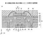
図1は、第1の実施の形態に係る半導体パッケージを例示する断面図である。図1を参照するに、半導体パッケージ10は、大略すると、配線基板30と、半導体チップ40と、ボンディングワイヤ45と、封止樹脂49とを有する。
<First Embodiment>
[Structure of Semiconductor Package According to First Embodiment]
FIG. 1 is a cross-sectional view illustrating a semiconductor package according to the first embodiment. Referring to FIG. 1, the
配線基板30は、半導体チップを内蔵したチップ内蔵型配線基板であり、大略すると、半導体チップ20と、配線層31と、絶縁層32と、配線層33と、絶縁層34と、配線層35と、絶縁層36と、配線層37と、ソルダーレジスト層38とを有する。
The
なお、半導体パッケージ10は、搭載状態に応じて上下方向が異なるが、便宜上、絶縁層32側を下、封止樹脂49側を上として説明を行う。従って、例えば絶縁層32の絶縁層34と接する面は上面であり、絶縁層32の露出面(絶縁層34と接する面の反対面)は下面である(他の実施の形態についても同様)。
Although the
半導体パッケージ10の平面形状は例えば矩形状であり、その寸法は、例えば幅10mm(X方向)×奥行き10mm(Y方向)×厚さ0.5mm(Z方向)程度とすることができる。以下、半導体パッケージ10を構成する半導体チップ20等について詳説する。
The planar shape of the
半導体チップ20は、半導体基板21と、電極パッド22と、突起電極23とを有する。半導体チップ20の平面形状は例えば矩形状であり、その寸法は、例えば幅5mm(X方向)×奥行き5mm(Y方向)×厚さ100μm(Z方向)程度とすることができる。
The
半導体基板21は、例えばシリコン(Si)を主成分とする基板に半導体集積回路(図示せず)が形成されたものである。電極パッド22は、半導体基板21の回路形成面側に形成されており、半導体集積回路(図示せず)と電気的に接続されている。電極パッド22の材料としては、例えばアルミニウム(Al)等を用いることができる。電極パッド22の材料として、銅(Cu)とアルミニウム(Al)をこの順番で積層したもの、銅(Cu)とアルミニウム(Al)とシリコン(Si)をこの順番で積層したもの等を用いても構わない。
The
突起電極23は電極パッド22上に形成されている。突起電極23としては、例えば円柱形状の銅(Cu)ポスト等を用いることができる。突起電極23の直径は、例えば50μm程度とすることができる。突起電極23の高さは、例えば5〜10μm程度とすることができる。突起電極23のピッチは、例えば100μm程度とすることができる。なお、電極パッド22上に突起電極23を設けなくてもよい。この場合には、電極パッド22自体が配線層33と電気的に接続される電極となる。
The protruding
以降、半導体チップ20において、回路形成面と反対側に位置する回路形成面と略平行な面を裏面と称する場合がある。又、半導体チップ20において、回路形成面及び裏面と略垂直な面を側面と称する場合がある。
Hereinafter, in the
半導体チップ20の回路形成面及び側面は絶縁層32に封止されており、裏面に貼り付けられたダイアタッチフィルム等の接着層24は絶縁層32から露出している。半導体チップ20の裏面に貼り付けられた接着層24は、絶縁層32の下面と略面一とされている。接着層24の厚さは数10μm程度であるから、半導体チップ20の裏面は、絶縁層32の下面と略面一であると考えて構わない。
The circuit formation surface and side surfaces of the
なお、図1では、半導体チップ20の裏面に接着層24が貼り付けられた状態を図示しているが、接着層24はプラズマ処理等により除去されている場合もある。この場合には、半導体チップ20の裏面は絶縁層32から露出する。
1 illustrates a state in which the
配線層31は、第1層31a及び第2層31bを有する。第1層31aとしては、例えば金(Au)膜、パラジウム(Pd)膜、ニッケル(Ni)膜を、金(Au)膜が半導体パッケージ10の外部に露出するように、この順番で順次積層した導電層を用いることができる。第1層31aとして、例えば金(Au)膜とニッケル(Ni)膜を、金(Au)膜が半導体パッケージ10の外部に露出するように、この順番で順次積層した導電層を用いてもよい。第2層31bとしては、例えば銅(Cu)層等を含む導電層を用いることができる。配線層31の厚さは、例えば10〜20μm程度とすることができる。
The
配線層31の一部(第1層31aの下面)は絶縁層32から露出しており、絶縁層32の下面及び半導体チップ20の裏面に貼り付けられた接着層24(半導体チップ20の裏面)と略面一とされている。配線層31の一部(第1層31aの下面)は、他の半導体パッケージや半導体チップ、マザーボード等の実装基板、或いは電子部品等(図示せず)と電気的に接続される電極パッドとして機能する。以降、絶縁層32から露出する配線層31を第1電極パッド31と称する場合がある。
A part of the wiring layer 31 (the lower surface of the
なお、図1では、第1電極パッド31は図面を簡略化するために数量を減らして描かれているが、実際には、例えば、複数列の第1電極パッド31が、平面視において半導体チップ20の裏面を額縁状に取り囲むように設けられている。第1電極パッド31の平面形状は例えば円形であり、その直径は例えば100〜350μm程度とすることができる。第1電極パッド31のピッチは、例えば400〜500μm程度とすることができる。
In FIG. 1, the
絶縁層32は、配線層31の上面及び側面、並びに、半導体チップ20の回路形成面及び側面を封止し、配線層31の下面及び接着層24を露出するように形成されている。絶縁層32の材料としては、例えばエポキシ系樹脂やフェノール系樹脂等を主成分とする熱硬化性の絶縁性樹脂を用いることができる。絶縁層32の厚さは、例えば150μm程度とすることができる。絶縁層32は、シリカ(SiO2)等のフィラーを含有しても構わない。絶縁層32は、本発明に係る第1の封止絶縁層の代表的な一例である。
The insulating
絶縁層32には、絶縁層32を貫通し配線層31の上面を露出するビアホール32x、及び絶縁層32を貫通し突起電極23の上面を露出するビアホール32yが形成されている。ビアホール32xは、絶縁層34側に開口されていると共に、配線層31の上面によって底面が形成された、開口部の面積が底面の面積よりも大となる円錐台状の凹部となっている。ビアホール32xの開口部の径は、例えば150μm程度とすることができる。
In the insulating
ビアホール32yは、絶縁層34側に開口されていると共に、突起電極23の上面によって底面が形成された、開口部の面積が底面の面積よりも大となる円錐台状の凹部となっている。ビアホール32yの開口部の径は、例えば30μm程度とすることができる。
The via
配線層33は、絶縁層32上に形成されている。配線層33は、ビアホール32xの側壁及び配線層31の上面に形成された第1ビア配線(貫通配線)、ビアホール32y内に充填された第2ビア配線(貫通配線)、及び絶縁層32上に形成された配線パターンを含んでいる。
The
配線層33は、ビアホール32xの底部に露出した配線層31、及びビアホール32yの底部に露出した突起電極23と電気的に接続されている。配線層33の材料としては、例えば銅(Cu)を主成分として含む金属材料等を用いることができる。配線層33を構成する配線パターンの厚さは、例えば10〜20μm程度とすることができる。
The
なお、例えば、絶縁層32の厚さを150μm、配線層31の厚さを10μmとすれば、ビアホール32xの深さは140μmとなり、第1ビア配線をビアホール32x内に充填することは困難である。そのため、第1ビア配線は、ビアホール32xの側壁及び配線層31の上面のみに膜状に形成され、ビアホール32x内に充填されてはいない。一方、例えば、絶縁層32の厚さを150μm、半導体チップ20の厚さ(突起電極23の高さも含む)を100μmとすれば、ビアホール32yの深さは50μmとなり、ビアホール32xよりも大幅に浅い。そのため、第2ビア配線は、ビアホール32y内に充填されている。
For example, if the thickness of the insulating
絶縁層34は、絶縁層32上に、配線層33を覆うように形成されている。絶縁層34の材料としては、絶縁層32と同様の絶縁性樹脂を用いることができる。絶縁層34の厚さは、例えば15〜35μm程度とすることができる。絶縁層34は、シリカ(SiO2)等のフィラーを含有しても構わない。
The insulating
配線層35は、絶縁層34上に形成されている。配線層35は、絶縁層34を貫通し配線層33の上面を露出するビアホール34x内に充填されたビア配線、及び絶縁層34上に形成された配線パターンを含んで構成されている。ビアホール34xは、絶縁層36側に開口されていると共に、配線層33の上面によって底面が形成された、開口部の面積が底面の面積よりも大となる円錐台状の凹部となっている。又、この凹部内にビア配線が形成されている。
The
配線層35は、ビアホール34xの底部に露出した配線層33と電気的に接続されている。配線層35の材料としては、例えば銅(Cu)を主成分として含む金属材料等を用いることができる。配線層35を構成する配線パターンの厚さは、例えば10〜20μm程度とすることができる。
The
絶縁層36は、絶縁層34上に、配線層35を覆うように形成されている。絶縁層36の材料としては、絶縁層32と同様の絶縁性樹脂を用いることができる。絶縁層36の厚さは、例えば15〜35μm程度とすることができる。絶縁層36は、シリカ(SiO2)等のフィラーを含有しても構わない。
The insulating
配線層37は、絶縁層36上に形成されている。配線層37は、絶縁層36を貫通し配線層35の上面を露出するビアホール36x内に充填されたビア配線、及び絶縁層36上に形成された配線パターンを含んで構成されている。ビアホール36xは、ソルダーレジスト層38側に開口されていると共に、配線層35の上面によって底面が形成された、開口部の面積が底面の面積よりも大となる円錐台状の凹部となっている。又、この凹部内にビア配線が形成されている。
The
配線層37は、ビアホール36xの底部に露出した配線層35と電気的に接続されている。配線層37の材料としては、例えば銅(Cu)を主成分として含む金属材料等を用いることができる。配線層37を構成する配線パターンの厚さは、例えば10〜20μm程度とすることができる。
The
ソルダーレジスト層38は、絶縁層36上に、配線層37を覆うように形成されている絶縁層である。ソルダーレジスト層38の厚さは、例えば15〜35μm程度とすることができる。ソルダーレジスト層38は、シリカ(SiO2)等のフィラーを含有しても構わない。ソルダーレジスト層38は開口部38xを有し、開口部38xの底部には配線層37の一部が露出している。
The solder resist
開口部38xの底部に露出する配線層37は、半導体チップ40と電気的に接続される電極パッドとして機能する。以降、開口部38xの底部に露出する配線層37を第2電極パッド37と称する場合がある。第2電極パッド37の平面形状は例えば円形であり、その直径は例えば100〜350μm程度とすることができる。第2の電極パッド37のピッチは、例えば400〜500μm程度とすることができる。
The
必要に応じ、第2電極パッド37上に、金属層を形成してもよい。金属層の例としては、Au層や、Ni/Au層(Ni層とAu層をこの順番で積層した金属層)、Ni/Pd/Au層(Ni層とPd層とAu層をこの順番で積層した金属層)等を挙げることができる。なお、ソルダーレジスト層を単に絶縁層と称する場合がある。
A metal layer may be formed on the
半導体チップ40は、配線基板30上に搭載されている。半導体チップ40は、半導体基板41と、電極パッド42とを有する。半導体チップ40の平面形状は例えば矩形状であり、その寸法は、例えば幅8mm(X方向)×奥行き8mm(Y方向)×厚さ200μm(Z方向)程度とすることができる。
The
半導体基板41は、例えばシリコン(Si)を主成分とする基板に半導体集積回路(図示せず)が形成されたものである。電極パッド42は、半導体基板41の回路形成面側に形成されており、半導体集積回路(図示せず)と電気的に接続されている。電極パッド42のピッチは、例えば100μm程度とすることができる。
The
電極パッド42の材料としては、例えばアルミニウム(Al)等を用いることができる。電極パッド42の材料として、銅(Cu)とアルミニウム(Al)をこの順番で積層したもの、銅(Cu)とアルミニウム(Al)とシリコン(Si)をこの順番で積層したもの等を用いても構わない。
As a material of the
半導体チップ40は、ダイアタッチフィルム等の接着層43を介して、ソルダーレジスト層38上に固着されている。半導体チップ40の電極パッド42は、例えば金(Au)や銅(Cu)等からなる導電性の細線であるボンディングワイヤ45を介して、配線基板30の第2電極パッド37に接合されている。
The
封止樹脂49は、半導体チップ40の回路形成面及び側面、並びにボンディングワイヤ45を被覆するように形成されている。封止樹脂49の材料としては、例えば熱硬化性のエポキシ系樹脂やポリイミド系樹脂等の絶縁性樹脂(モールド樹脂)を用いることができる。封止樹脂49の材料は、シリカ(SiO2)等のフィラーを含有しても構わない。封止樹脂49の厚さは、例えば300〜400μm程度とすることができる。
The sealing
なお、封止樹脂49は、半導体チップ40やボンディングワイヤ45を外部からの応力や湿気、汚染物質等から守る機能と、半導体パッケージ10の機械的強度を向上する機能を有する。しかし、半導体チップ40を搭載したことにより、半導体パッケージ10全体の機械的強度を向上できるため、必ずしも封止樹脂49を設けなくてもよい。封止樹脂49は、本発明に係る第2の封止絶縁層の代表的な一例である。
The sealing
[第1の実施の形態に係る半導体パッケージの製造方法]
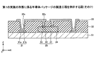
次に、第1の実施の形態に係る半導体パッケージの製造方法について説明する。図2〜図12は、第1の実施の形態に係る半導体パッケージの製造工程を例示する図である。
[Method of Manufacturing Semiconductor Package According to First Embodiment]
Next, a method for manufacturing a semiconductor package according to the first embodiment will be described. 2 to 12 are diagrams illustrating the manufacturing process of the semiconductor package according to the first embodiment.
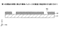
まず、図2〜図10に示す工程では、配線基板30を作製する。最初に、図2に示す工程では、支持体51を準備し、支持体51の一方の面に、配線層31に対応する開口部52xを有するレジスト層52を形成する。支持体51としては、シリコン板、ガラス板、金属板、金属箔等を用いることができるが、本実施の形態では、支持体51として銅箔を用いる。後述する図3に示す工程等において電解めっきを行う際の給電層として利用でき、後述する図12に示す工程の後に容易にエッチングで除去可能だからである。支持体51の厚さは、例えば35〜100μm程度とすることができる。
First, in the steps shown in FIGS. 2 to 10, the
開口部52xを有するレジスト層52を形成するには、支持体51の一方の面に、例えばエポキシ系樹脂やアクリル系樹脂等を含む感光性樹脂組成物からなる液状又はペースト状のレジストを塗布する。或いは、支持体51の一方の面に、例えばエポキシ系樹脂やアクリル系樹脂等を含む感光性樹脂組成物からなるフィルム状のレジスト(例えば、ドライフィルムレジスト等)をラミネートする。
In order to form the resist
そして、塗布又はラミネートしたレジストを露光及び現像することで開口部52xを形成する。これにより、開口部52xを有するレジスト層52が形成される。なお、予め開口部52xを形成したフィルム状のレジストを支持体51の一方の面にラミネートしても構わない。開口部52xは、後述の図3に示す工程で形成される配線層31に対応する位置に形成される。開口部52xの平面形状は、例えば円形であり、その直径は例えば100〜350μm程度とすることができる。
Then, the
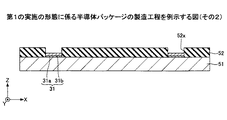
次に、図3に示す工程では、支持体51をめっき給電層に利用する電解めっき法等により、支持体51の一方の面の開口部52x内に、第1層31a及び第2層31bから構成される配線層31を形成する。第1層31aは、例えば金(Au)膜、パラジウム(Pd)膜、ニッケル(Ni)膜をこの順番で順次積層した構造を有する。
Next, in the step shown in FIG. 3, the
よって、配線層31を形成するには、まず、支持体51をめっき給電層に利用する電解めっき法等により、金(Au)膜、パラジウム(Pd)膜、ニッケル(Ni)膜を順にめっきして第1層31aを形成する。続いて、支持体51をめっき給電層に利用する電解めっき法等により、第1層31a上に銅(Cu)等からなる第2層31bを形成すればよい。なお、第1層31aは、金(Au)膜とニッケル(Ni)膜をこの順番で順次積層した構造としてもよい。
Therefore, in order to form the
次に、図4に示す工程では、半導体チップ20を準備する。そして、図3に示すレジスト層52を除去した後、支持体51の一方の面に、ダイアタッチフィルム等の接着層24を介して、半導体チップ20をフェイスアップの状態(回路形成面を上にした状態)で配置する。半導体チップ20は、半導体基板21と、電極パッド22と、突起電極23とを有し、電極パッド22及び突起電極23は半導体チップ20の回路形成面側に形成されている。又、半導体チップ20は、例えば100μm程度に薄型化されている。
Next, in the step shown in FIG. 4, the
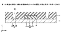
次に、図5に示す工程では、半導体チップ20の回路形成面及び側面、並びに、配線層31の上面及び側面を封止するように、支持体51の一方の面に絶縁層32を形成する。絶縁層32の材料としては、例えばエポキシ系樹脂やフェノール系樹脂等を主成分とする熱硬化性の絶縁性樹脂を用いることができる。絶縁層32の厚さは、例えば150μm程度とすることができる。絶縁層32は、シリカ(SiO2)等のフィラーを含有しても構わない。
Next, in the process shown in FIG. 5, the insulating
絶縁層32の材料として、例えば熱硬化性を有するフィルム状のエポキシ系樹脂やフェノール系樹脂等を主成分とする絶縁性樹脂を用いた場合には、以下のようにする。すなわち、半導体チップ20の回路形成面及び側面、並びに、配線層31の上面及び側面を封止するように、支持体51の一方の面に半硬化状態のフィルム状の絶縁層32をラミネートする。そして、ラミネートした絶縁層32を押圧しつつ、絶縁層32を硬化温度以上に加熱して硬化させる。なお、絶縁層32を真空雰囲気中でラミネートすることにより、ボイドの巻き込みを防止できる。
When an insulating resin mainly composed of a thermosetting film-like epoxy resin, phenol resin, or the like is used as the material of the insulating
絶縁層32の材料として、例えば熱硬化性を有する液状又はペースト状のエポキシ系樹脂やフェノール系樹脂等を主成分とする絶縁性樹脂を用いた場合には、以下のようにする。すなわち、半導体チップ20の回路形成面及び側面、並びに、配線層31の上面及び側面を封止するように、支持体51の一方の面に液状又はペースト状の絶縁層32を例えばロールコート法等により塗布する。そして、塗布した絶縁層32を硬化温度以上に加熱して硬化させる。
When the insulating
次に、図6に示す工程では、絶縁層32に、絶縁層32を貫通し配線層31の上面を露出させるビアホール32xを形成する。ビアホール32xは、例えばCO2レーザ等を用いたレーザ加工法により形成できる。レーザ加工法により形成したビアホール32xは、絶縁層34が形成される側に開口されていると共に、配線層31の上面によって底面が形成された、開口部の面積が底面の面積よりも大となる円錐台状の凹部となる。ビアホール32xの開口部の径は、例えば150μm程度とすることができる。
Next, in the process shown in FIG. 6, a via
次に、図7に示す工程では、絶縁層32に、絶縁層32を貫通し突起電極23の上面を露出するビアホール32yを形成する。ビアホール32yは、例えばUVレーザ等を用いたレーザ加工法により形成できる。レーザ加工法により形成したビアホール32yは、絶縁層34が形成される側に開口されていると共に、突起電極23の上面によって底面が形成された、開口部の面積が底面の面積よりも大となる円錐台状の凹部となる。ビアホール32yの開口部の径は、例えば30μm程度とすることができる。
Next, in the step shown in FIG. 7, a via
なお、ビアホール32x及びビアホール32yをレーザ加工法により形成した場合には、図7に示す工程後にデスミア処理を行うことが好ましい。ビアホール32xの底部に露出する配線層31の上面、及びビアホール32yの底部に露出する突起電極23の上面に付着した絶縁層32の樹脂残渣を除去するためである。
When the via
次に、図8に示す工程では、絶縁層32上に配線層33を形成する。配線層33は、ビアホール32xの側壁及び配線層31の上面に形成された第1ビア配線、ビアホール32y内に充填された第2ビア配線、及び絶縁層32上に形成された配線パターンを含んでいる。配線層33は、ビアホール32xの底部に露出した配線層31、及びビアホール32yの底部に露出した突起電極23と電気的に接続される。
Next, in the step shown in FIG. 8, the
配線層33の材料としては、例えば銅(Cu)を主成分として含む金属材料等を用いることができる。配線層33を構成する配線パターンの厚さは、例えば10〜20μm程度とすることができる。なお、前述の理由により、第1ビア配線はビアホール32x内に充填されてはいないが、第2ビア配線はビアホール32y内に充填されている。
As a material of the
配線層33は、セミアディティブ法やサブトラクティブ法等の各種の配線形成方法を用いて形成できるが、一例としてセミアディティブ法を用いて配線層33を形成する方法を以下に示す。
The
まず、ビアホール32xの内部に露出した配線層31の上面及びビアホール32yの内部に露出した突起電極23の上面、並びに、ビアホール32xの側壁及びビアホール32yの側壁を含む絶縁層32上にシード層(図示せず)を形成する。例えば、無電解めっき法又はスパッタ法により、銅(Cu)を主成分として含む金属材料等からなるシード層(図示せず)を形成できる。次に、シード層上に配線層33に対応する開口部を備えたレジスト層(図示せず)を形成する。
First, the seed layer (see FIG. 3) is formed on the upper surface of the
そして、シード層を給電層に利用した電解めっき法により、レジスト層の開口部に銅(Cu)を主成分として含む金属材料等からなる配線層(図示せず)を形成する。続いて、レジスト層を除去した後に、配線層をマスクにして、配線層に覆われていない部分のシード層をエッチングにより除去する。これにより、ビアホール32xの側壁及び配線層31の上面に形成された第1ビア配線、ビアホール32y内に充填された第2ビア配線、及び絶縁層32上に形成された配線パターンを含む配線層33が形成される。
Then, a wiring layer (not shown) made of a metal material containing copper (Cu) as a main component is formed in the opening of the resist layer by an electrolytic plating method using the seed layer as a power feeding layer. Subsequently, after removing the resist layer, the seed layer not covered with the wiring layer is removed by etching using the wiring layer as a mask. As a result, the first via wiring formed on the sidewall of the via
次に、図9に示す工程では、上記と同様な工程を繰り返すことにより、絶縁層32上に、絶縁層34、配線層35、絶縁層36、配線層37を積層する。すなわち、絶縁層32上に配線層33を被覆する絶縁層34を形成した後に、絶縁層34を貫通し配線層33の上面を露出するビアホール34xを形成する。絶縁層34の材料としては、絶縁層32と同様の絶縁性樹脂を用いることができる。絶縁層34の厚さは、例えば15〜35μm程度とすることができる。絶縁層34は、シリカ(SiO2)等のフィラーを含有しても構わない。
Next, in the process shown in FIG. 9, the insulating
更に、絶縁層34上に、ビアホール34xを介して配線層33に接続される配線層35を形成する。配線層35は、ビアホール34x内を充填するビア配線、及び絶縁層34上に形成された配線パターンを含んで構成されている。配線層35は、ビアホール34xの底部に露出した配線層33と電気的に接続される。配線層35の材料としては、例えば銅(Cu)を主成分として含む金属材料等を用いることができる。配線層35は、例えばセミアディティブ法により形成される。配線層35を構成する配線パターンの厚さは、例えば10〜20μm程度とすることができる。
Further, a
更に、絶縁層34上に配線層35を被覆する絶縁層36を形成した後に、絶縁層36を貫通し配線層35の上面を露出するビアホール36xを形成する。絶縁層36の材料としては、絶縁層34と同様の絶縁性樹脂を用いることができる。絶縁層36の厚さは、例えば15〜35μm程度とすることができる。絶縁層36は、シリカ(SiO2)等のフィラーを含有しても構わない。
Further, an insulating
更に、絶縁層36上に、ビアホール36xを介して配線層35に接続される配線層37を形成する。配線層37は、ビアホール36x内を充填するビア配線、及び絶縁層36上に形成された配線パターンを含んで構成されている。配線層37は、ビアホール36xの底部に露出した配線層35と電気的に接続される。配線層37の材料としては、例えば銅(Cu)を主成分として含む金属材料等を用いることができる。配線層37は、例えばセミアディティブ法により形成される。配線層37を構成する配線パターンの厚さは、例えば10〜20μm程度とすることができる。
Further, a
このようにして、支持体51の一方の面に所定のビルドアップ配線層が形成される。本実施の形態では、3層のビルドアップ配線層(配線層33、配線層35、及び配線層37)を形成したが、n層(nは1以上の整数)のビルドアップ配線層を形成してもよい。
In this way, a predetermined build-up wiring layer is formed on one surface of the
次に、図10に示す工程では、絶縁層36上に、配線層37の一部を露出する開口部38xを有するソルダーレジスト層38を形成し、配線基板30を作製する。ソルダーレジスト層38は、例えば液状又はペースト状の感光性のエポキシ系やアクリル系の絶縁性樹脂を、配線層37を被覆するように絶縁層36上にスクリーン印刷法、ロールコート法、又は、スピンコート法等で塗布することにより形成できる。或いは、例えばフィルム状の感光性のエポキシ系やアクリル系の絶縁性樹脂を、配線層37を被覆するように絶縁層36上にラミネートすることにより形成してもよい。
Next, in the step shown in FIG. 10, a solder resist
開口部38xは、塗布又はラミネートした絶縁性樹脂を露光及び現像することすることにより形成できる(フォトリソグラフィ法)。予め開口部38xを形成したフィルム状の絶縁性樹脂を、配線層37を被覆するように絶縁層36上にラミネートしても構わない。なお、ソルダーレジスト層38の材料として、非感光性の絶縁性樹脂を用いてもよい。この場合には、絶縁層36上にソルダーレジスト層38を形成して硬化させた後、例えばCO2レーザ等を用いたレーザ加工法や、アルミナ砥粒等の研磨剤を用いたブラスト処理により開口部38xを形成すればよい。
The
必要に応じ、開口部38xの底部に露出する配線層37上に、例えば無電解めっき法等により金属層を形成してもよい。金属層の例としては、Au層や、Ni/Au層(Ni層とAu層をこの順番で積層した金属層)、Ni/Pd/Au層(Ni層とPd層とAu層をこの順番で積層した金属層)等を挙げることができる。
If necessary, a metal layer may be formed on the
次に、図11に示す工程では、半導体チップ40を準備する。そして、ソルダーレジスト層38上に、ダイアタッチフィルム等の接着層43を介して、半導体チップ40をフェイスアップの状態(回路形成面を上にした状態)で配置する。そして、半導体チップ40の電極パッド42を、例えば金(Au)や銅(Cu)等からなる導電性の細線であるボンディングワイヤ45を介して、第2電極パッド37に接合する。半導体チップ40は、半導体基板41と、電極パッド42とを有し、電極パッド42は半導体チップ40の回路形成面側に形成されている。又、半導体チップ40は、例えば200μm程度に薄型化されている。
Next, in the step shown in FIG. 11, the
次に、図12に示す工程では、半導体チップ40の回路形成面及び側面、並びにボンディングワイヤ45を被覆するように封止樹脂49を形成する。封止樹脂49は、例えば、トランスファーモールド法等により形成できる。封止樹脂49の材料としては、例えば熱硬化性のエポキシ系樹脂やポリイミド系樹脂等の絶縁性樹脂(モールド樹脂)を用いることができる。封止樹脂49の材料は、シリカ(SiO2)等のフィラーを含有しても構わない。封止樹脂49の厚さは、例えば300〜400μm程度とすることができる。
Next, in the step shown in FIG. 12, a sealing
次に、図12に示す工程の後(図示せず)、図12に示す支持体51を除去することにより、図1に示す半導体パッケージ10が完成する。銅箔から構成されている支持体51は、例えば塩化第二鉄水溶液や塩化第二銅水溶液、過硫酸アンモニウム水溶液、塩化アンモニウム銅水溶液、過酸化水素水・硫酸系のエッチング液等を用いたウェットエッチングにより除去できる。この際、絶縁層32から露出する配線層31の最表層は金(Au)膜等であり、絶縁層32から露出する半導体チップ20の裏面には接着層24が貼り付けられているため、銅箔から構成されている支持体51のみを選択的にエッチングできる。
Next, after the step shown in FIG. 12 (not shown), the
なお、支持体51を除去した後、プラズマ処理等により、半導体チップ20の裏面に貼り付けられている接着層24を除去し、半導体チップ20の裏面を絶縁層32から露出させてもよい。
Note that after removing the
半導体パッケージ10は、一方の側に半導体チップ20を有し、他方の側に半導体チップ40を有する。半導体チップ20及び40が、例えば、それぞれシリコン(Si)を主成分とする場合、その熱膨張係数は3.4ppm/℃程度、ヤング率は200GPa程度である。
The
つまり、半導体パッケージ10は、熱膨張係数が小さくヤング率の高い部材がおおよそ上下対称に配置された構造であり、上下方向で物性値(熱膨張係数やヤング率)のバランスがとれている。これにより、従来の半導体パッケージの問題点であった、半導体チップが内蔵されている側は熱応力等により変形し難いが、半導体チップが内蔵されていない側は熱応力等により変形し易いという現象が生じ難い。従って、図12に示す工程の後に支持体51を除去しても、大きな反りが生ることはない。
That is, the
なお、図2〜図12では、支持体51上に1個の半導体パッケージ10を作製する例を示した。しかし、支持体51上に複数の半導体パッケージ10となる部材を作製し、支持体51を除去後、該部材を切断して個片化し、複数の半導体パッケージ10を得るような工程としても構わない。又、個片化の際に、複数の半導体チップ20及び40を有するように切断しても構わない。その場合には、複数の半導体チップ20及び40を有する半導体パッケージが作製される。
2 to 12 show an example in which one
このように、第1の実施の形態に係る半導体パッケージは、熱膨張係数が小さくヤング率の高い部材がおおよそ上下対称に配置された構造であり、上下方向で物性値(熱膨張係数やヤング率)のバランスがとれている。これにより、熱応力等により発生する反りを低減できる。 As described above, the semiconductor package according to the first embodiment has a structure in which members having a small coefficient of thermal expansion and a high Young's modulus are arranged approximately vertically. Physical property values (thermal expansion coefficient and Young's modulus in the vertical direction). ) Is balanced. Thereby, the curvature generate | occur | produced by a thermal stress etc. can be reduced.
又、熱膨張係数が小さくヤング率の高い部材がおおよそ上下対称に配置されているため、半導体パッケージ全体の機械的強度を向上できる。 In addition, since the members having a small thermal expansion coefficient and a high Young's modulus are arranged approximately vertically, the mechanical strength of the entire semiconductor package can be improved.
又、第1の実施の形態に係る半導体パッケージ10の製造方法は、支持体51を除去する前に、半導体チップ20の反対側となる配線基板30のソルダーレジスト層38上に半導体チップ40を搭載している。そのため、剛性の高い半導体チップ20と剛性の高い半導体チップ40が上下対称に配置された構造となり、上下方向で物性値(熱膨張係数やヤング率)のバランスがとれる。その結果、支持体51を除去する際に配線基板30が大きく反ることを防止できる。
Further, in the method of manufacturing the
なお、配線基板上に半導体チップをボンディングワイヤを介して接続する際には、配線基板上に半導体チップをフリップチップ接続する際のように加熱する必要がない。そのため、配線基板上に半導体チップをボンディングワイヤを介して接続する方法は、配線基板の反りや歪みの低減に有利である。 In addition, when connecting a semiconductor chip on a wiring board via a bonding wire, it is not necessary to heat like the case where a semiconductor chip is flip-chip connected on a wiring board. Therefore, a method of connecting a semiconductor chip on a wiring board via a bonding wire is advantageous for reducing warping and distortion of the wiring board.
〈第1の実施の形態の変形例1〉
第1の実施の形態の変形例1では、半導体パッケージの第1の実施の形態とは異なる製造方法の例を示す。なお、第1の実施の形態の変形例1において、既に説明した実施の形態と同一構成部品についての説明は省略する。
<Variation 1 of the first embodiment>
In the first modification of the first embodiment, an example of a manufacturing method different from that of the first embodiment of the semiconductor package is shown. In the first modification of the first embodiment, the description of the same components as those of the already described embodiment is omitted.
図13及び図14は、第1の実施の形態に係る半導体パッケージの他の製造工程を例示する図である。 13 and 14 are diagrams illustrating another manufacturing process of the semiconductor package according to the first embodiment.
まず、図13に示す工程では、支持体511及び512を接着剤等により上下に張り合わせた支持体55を準備する。支持体511及び512としては、シリコン板、ガラス板、金属板、金属箔等を用いることができるが、本実施の形態では、支持体511及び512として銅箔を用いる。支持体511及び512のそれぞれの厚さは、例えば35〜100μm程度とすることができる。
In the step shown in FIG. 13, to prepare a
次に、図14に示す工程では、第1の実施の形態の図2〜図12と同様の工程を実行し、支持体511の上面に半導体パッケージ10に対応する構造体を作製する。又、支持体512の下面に半導体パッケージ10に対応する構造体を作製する。
Next, in a step shown in FIG. 14, and step similar to FIGS. 2 to 12 of the first embodiment, to produce a structure corresponding to the
次に、図14に示す工程の後(図示せず)、接着剤等を剥離して支持体55を支持体511と支持体512に分離することにより、図12に相当する構造体が2つ作製される。その後、2つの図12に相当する構造体から支持体511又は支持体512を除去することにより、2つの半導体パッケージ10を形成できる。
Next, (not shown) after the step shown in FIG. 14, by separating the to support 55 peel an adhesive to the
このように、支持体511及び512を上下に張り合わせた支持体55を準備し、支持体511の上面及び支持体512の下面に配線基板30等を同時に形成する。その後、支持体55を支持体511と支持体512に分離し、支持体511及び512を除去することにより、1連の製造工程で2つの半導体パッケージ10を形成できる。
Thus, to prepare a
〈第1の実施の形態の変形例2〉
第1の実施の形態の変形例2では、配線基板上に半導体チップをフリップチップ接続する例を示す。なお、第1の実施の形態の変形例2において、既に説明した実施の形態と同一構成部品についての説明は省略する。
<Modification 2 of the first embodiment>
The second modification of the first embodiment shows an example in which a semiconductor chip is flip-chip connected to a wiring board. In the second modification of the first embodiment, the description of the same components as those of the already described embodiment is omitted.
図15は、第1の実施の形態の変形例2に係る半導体パッケージを例示する断面図である。図15を参照するに、半導体パッケージ10Aは、配線基板30にボンディングワイヤ45を介して接続された半導体チップ40が、配線基板30にフリップチップ接続された半導体チップ60に置換された点が、半導体パッケージ10(図1参照)と相違する。
FIG. 15 is a cross-sectional view illustrating a semiconductor package according to Modification 2 of the first embodiment. Referring to FIG. 15, the
半導体チップ60は、半導体基板61と、電極パッド62とを有する。半導体基板61及び電極パッド62については、半導体チップ40の半導体基板41及び電極パッド42と同様であるため、その説明は省略する。半導体チップ40とは異なり、半導体チップ60はフェイスダウンの状態(回路形成面を下にした状態)で、配線基板30に搭載されている。具体的には、半導体チップ60の電極パッド62は、接合部65を介して、配線基板30の第2電極パッド37と電気的に接続されている。
The
接合部65としては、例えば、はんだボール等を用いることができる。はんだボールの材料としては、例えばPbを含む合金、SnとCuの合金、SnとSbの合金、SnとAgの合金、SnとAgとCuの合金等を用いることができる。 半導体チップ60は、封止樹脂49により封止されている。放熱性を向上するため、半導体チップ60の裏面を封止樹脂49から露出させてもよい。但し、第1の実施の形態と同様の理由により、必ずしも封止樹脂49を設けなくてもよい。なお、半導体チップ60と配線基板30との間に、アンダーフィル樹脂を設けてもよい。
As the joining
このように、配線基板上に半導体チップをフリップチップ接続しても、第1の実施の形態と同様の効果を奏する。 Thus, even if the semiconductor chip is flip-chip connected to the wiring board, the same effects as those of the first embodiment are obtained.
〈第1の実施の形態の変形例3〉
第1の実施の形態の変形例3では、配線基板上に半導体チップを異方性導電フィルムを用いて接続する例を示す。なお、第1の実施の形態の変形例3において、既に説明した実施の形態と同一構成部品についての説明は省略する。
<
図16は、第1の実施の形態の変形例3に係る半導体パッケージを例示する断面図である。図16を参照するに、半導体パッケージ10Bは、配線基板30にボンディングワイヤ45を介して接続された半導体チップ40が、配線基板30に異方性導電フィルムを用いて接続された半導体チップ60に置換された点が、半導体パッケージ10(図1参照)と相違する。
FIG. 16 is a cross-sectional view illustrating a semiconductor package according to
半導体チップ40とは異なり、半導体チップ60はフェイスダウンの状態(回路形成面を下にした状態)で、配線基板30に搭載されている。具体的には、半導体チップ60の電極パッド62には、例えば円柱形状の銅ポスト等の突起電極63が形成されている。そして、突起電極63は、異方性導電フィルム69を介して、配線基板30の第2電極パッド37と電気的に接続されている。
Unlike the
異方性導電フィルム69としては、例えば、ニッケル(Ni)や金(Au)、銀(Ag)等の導電粒子を分散させた半硬化状態の樹脂フィルム(エポキシ系等の熱硬化性樹脂)を用いることができる。
As the anisotropic
半導体チップ60は、封止樹脂49により封止されている。放熱性を向上するため、半導体チップ60の裏面を封止樹脂49から露出させてもよい。但し、第1の実施の形態と同様の理由により、必ずしも封止樹脂49を設けなくてもよい。
The
異方性導電フィルム69を用いて半導体チップ60の突起電極63を配線基板30の第2電極パッド37と電気的に接続する方法を以下に示す。まず、配線基板30のソルダーレジスト層38上に、第2電極パッド37を被覆するように、半硬化状態の異方性導電フィルム69を貼着する(仮貼り付け)。
A method for electrically connecting the protruding
次に、半導体チップ60を準備する。そして、半導体チップ60の突起電極63を配線基板30の第2電極パッド37に位置合わせし、半導体チップ60の突起電極63と配線基板30の第2電極パッド37とが異方性導電フィルム69を介して対向する位置に来るように配置する。半導体チップ60の突起電極63と配線基板30の第2電極パッド37との位置合わせは、例えば、ボンディングツール等により行うことができる。
Next, the
次に、ボンディングツール等により、半導体チップ60を異方性導電フィルム69に対して押圧する。この際、ボンディングツール等により、半導体チップ60を加熱しながら異方性導電フィルム69に対する押圧を行い、半硬化状態の異方性導電フィルム69を硬化させる。
Next, the
この際、異方性導電フィルム69は、半導体チップ60の突起電極63と配線基板30の第2電極パッド37に挟持され圧縮される。そのため、異方性導電フィルム69中に分散された導電粒子が相互に接触し、半導体チップ60の突起電極63と配線基板30の第2電極パッド37とが導電粒子を介して電気的に接続される。
At this time, the anisotropic
このように、配線基板上に半導体チップを異方性導電フィルムを用いて接続しても、第1の実施の形態と同様の効果を奏する。 As described above, even if the semiconductor chip is connected to the wiring board using the anisotropic conductive film, the same effect as that of the first embodiment is obtained.
〈第1の実施の形態の変形例4〉
第1の実施の形態の変形例4では、配線基板上に半導体チップをフリップチップ接続し、更にその上に他の半導体チップをフリップチップ接続する例を示す。なお、第1の実施の形態の変形例4において、既に説明した実施の形態と同一構成部品についての説明は省略する。
<Modification 4 of the first embodiment>
Modification 4 of the first embodiment shows an example in which a semiconductor chip is flip-chip connected on a wiring board, and another semiconductor chip is further flip-chip connected thereon. Note that in the fourth modification of the first embodiment, the description of the same components as those of the already described embodiment is omitted.
図17は、第1の実施の形態の変形例4に係る半導体パッケージを例示する断面図である。図17を参照するに、半導体パッケージ10Cは、配線基板30にボンディングワイヤ45を介して接続された半導体チップ40が、配線基板30にフリップチップ接続された半導体チップ70及び80に置換された点が、半導体パッケージ10(図1参照)と相違する。
FIG. 17 is a cross-sectional view illustrating a semiconductor package according to Modification 4 of the first embodiment. Referring to FIG. 17, the
半導体チップ70は、半導体基板71と、電極パッド72及び74と、貫通電極73とを有する。半導体基板71の一方の側に電極パッド72が設けられ、他方の側に電極パッド74が設けられている。電極パッド72と電極パッド74とは貫通電極73を介して電気的に接続されている。
The
半導体基板71並びに電極パッド72及び74の詳細については、半導体チップ40の半導体基板41及び電極パッド42と同様であるため、その説明は省略する。貫通電極73の材料としては、例えば銅(Cu)を主成分として含む金属材料等を用いることができる。
The details of the
半導体チップ80は、半導体基板81と、電極パッド82とを有する。半導体基板81及び電極パッド82については、半導体チップ40の半導体基板41及び電極パッド42と同様であるため、その説明は省略する。
The
半導体チップ40とは異なり、半導体チップ70はフェイスダウンの状態(回路形成面を下にした状態)で、配線基板30に搭載されている。具体的には、半導体チップ70の電極パッド72は、はんだボール等の接合部65を介して、配線基板30の第2電極パッド37と電気的に接続されている。なお、電極パッド72は、半導体チップ70の半導体集積回路(図示せず)と電気的に接続されている。
Unlike the
半導体チップ80の電極パッド82は、接合部75を介して、半導体チップ70の電極パッド74と電気的に接続されている。接合部75としては、接合部65と同様に、はんだボール等を用いることができる。
The
半導体チップ70及び80は、封止樹脂49により封止されている。放熱性を向上するため、半導体チップ80の裏面を封止樹脂49から露出させてもよい。但し、第1の実施の形態と同様の理由により、必ずしも封止樹脂49を設けなくてもよい。
The semiconductor chips 70 and 80 are sealed with a sealing
このように、配線基板上にフリップチップ接続等により複数の半導体チップを積層しても、第1の実施の形態と同様の効果を奏する。 Thus, even when a plurality of semiconductor chips are stacked on the wiring board by flip chip connection or the like, the same effects as those of the first embodiment are obtained.
〈第1の実施の形態の変形例5〉
第1の実施の形態の変形例5では、配線基板上に、半導体集積回路が形成されていない板状体を搭載する例を示す。なお、第1の実施の形態の変形例5において、既に説明した実施の形態と同一構成部品についての説明は省略する。
<Modification 5 of the first embodiment>
The fifth modification of the first embodiment shows an example in which a plate-like body on which a semiconductor integrated circuit is not formed is mounted on a wiring board. Note that in the fifth modification of the first embodiment, the description of the same components as those of the already described embodiment will be omitted.
図18は、第1の実施の形態の変形例5に係る半導体パッケージを例示する断面図である。図18を参照するに、半導体パッケージ10Dは、配線基板30にボンディングワイヤ45を介して接続された半導体チップ40が、配線基板30に搭載された板状体90に置換された点が、半導体パッケージ10(図1参照)と相違する。
FIG. 18 is a cross-sectional view illustrating a semiconductor package according to Modification 5 of the first embodiment. Referring to FIG. 18, the
板状体90は、配線基板30のソルダーレジスト層38上に搭載され、封止樹脂49により封止されている。封止樹脂49には、第2電極パッド37を露出する貫通孔49xが形成されている。第2電極パッド37を露出する貫通孔49xを形成することにより、封止樹脂49上に貫通孔49xを介して第2電極パッド37と電気的に接続する半導体チップや電子部品(コンデンサ等)等を更に搭載することが可能となる。
The plate-
貫通孔49xの平面形状は例えば円形であり、その直径は例えば100〜350μm程度とすることができる。貫通孔49xは、例えば、貫通孔に対応した突起部を有する金型によるトランスファーモールド法や、レーザ加工法、ブラスト処理等により形成できる。
The planar shape of the through
但し、第1の実施の形態と同様の理由により、必ずしも封止樹脂49を設けなくてもよい。板状体90としては、例えば、半導体集積回路が形成されていない板状のシリコンやガラス、セラミック等の無機材料を用いることが好ましい。
However, the sealing
例えば、板状体90としてガラスの一種である硼珪酸ガラスを用いた場合の熱膨張係数は3ppm/℃程度である。又、板状体90としてセラミックの一種であるムライトを用いた場合の熱膨張係数(CTE)は4.5ppm/℃程度、アルミナを用いた場合の熱膨張係数(CTE)は6〜7ppm/℃程度である。
For example, the thermal expansion coefficient when borosilicate glass, which is a kind of glass, is used as the plate-
板状体90の厚さは、例えば、200μm程度とすることができる。なお、図18の例では、ソルダーレジスト層38上の一部の領域に板状体90を搭載しているが、ソルダーレジスト層38上の全面に板状体90を搭載してもよい。この場合には、板状体90及び封止樹脂49に第2電極パッド37を露出する貫通孔を形成すればよい。
The thickness of the plate-
このように、配線基板30上に、半導体チップに代えて、半導体チップと熱膨張係数の近い部材(板状体)を搭載しても第1の実施の形態と同様の効果を奏する。
As described above, even if a member (plate body) having a thermal expansion coefficient close to that of the semiconductor chip is mounted on the
なお、封止樹脂49上に半導体チップや電子部品(コンデンサ等)等を更に搭載しない場合には、開口部38x及び貫通孔49xは設けなくてよい。
Note that the
〈第1の実施の形態の変形例6〉
第1の実施の形態の変形例6では、配線基板上に半導体チップをフリップチップ接続して封止樹脂で封止し、封止樹脂に貫通孔を設ける例を示す。なお、第1の実施の形態の変形例6において、既に説明した実施の形態と同一構成部品についての説明は省略する。
<Modification 6 of the first embodiment>
The sixth modification of the first embodiment shows an example in which a semiconductor chip is flip-chip connected on a wiring board and sealed with a sealing resin, and a through hole is provided in the sealing resin. Note that in the sixth modification of the first embodiment, the description of the same components as those of the already described embodiment will be omitted.
図19は、第1の実施の形態の変形例6に係る半導体パッケージを例示する断面図である。図19を参照するに、半導体パッケージ10Eは、配線基板30にボンディングワイヤ45を介して接続された半導体チップ40が、配線基板30にフリップチップ接続された半導体チップ60に置換され、更に封止樹脂49に貫通孔49xが設けられた点が、半導体パッケージ10(図1参照)と相違する。
FIG. 19 is a cross-sectional view illustrating a semiconductor package according to Modification 6 of the first embodiment. Referring to FIG. 19, in the semiconductor package 10E, the
半導体チップ60はフェイスダウンの状態(回路形成面を下にした状態)で、配線基板30に搭載されている。具体的には、半導体チップ60の電極パッド62は、接合部65を介して、配線基板30の第2電極パッド37と電気的に接続されている。半導体チップ60は、封止樹脂49により封止されている。放熱性を向上するため、半導体チップ60の裏面を封止樹脂49から露出させてもよい。
The
封止樹脂49には貫通孔49xが設けられている。貫通孔49xはソルダーレジスト層38も貫通し、貫通孔49x内には配線層37の一部が露出している。貫通孔49x内に露出する配線層37は、封止樹脂49上に半導体チップや電子部品(コンデンサ等)等を更に搭載する際の電極パッドとして機能する。
The sealing
なお、封止樹脂49に代えてアンダーフィル樹脂を設けてもよい。この場合には、配線層37の電極パッドとなる部分を露出するようにアンダーフィル樹脂を設けることができる。
An underfill resin may be provided instead of the sealing
このように、配線基板上に半導体チップをフリップチップ接続して封止樹脂で封止し、封止樹脂に貫通孔を設けることにより、第1の実施の形態の効果に加えて、更に以下の効果を奏する。すなわち、封止樹脂49上に貫通孔49xを介して配線層37と電気的に接続する半導体チップや電子部品(コンデンサ等)等を更に搭載することが可能となる。
As described above, the semiconductor chip is flip-chip connected to the wiring substrate and sealed with the sealing resin, and the through hole is provided in the sealing resin, so that the following effects are further obtained. There is an effect. That is, it is possible to further mount a semiconductor chip, an electronic component (a capacitor, or the like) or the like that is electrically connected to the
〈第1の実施の形態の変形例7〉
第1の実施の形態の変形例7では、配線基板上に半導体チップをフリップチップ接続してアンダーフィル樹脂で封止する例を示す。なお、第1の実施の形態の変形例7において、既に説明した実施の形態と同一構成部品についての説明は省略する。
<Modification 7 of the first embodiment>
Modification 7 of the first embodiment shows an example in which a semiconductor chip is flip-chip connected on a wiring board and sealed with an underfill resin. Note that, in the modified example 7 of the first embodiment, the description of the same component as the already described embodiment is omitted.
図20は、第1の実施の形態の変形例7に係る半導体パッケージを例示する断面図である。図20を参照するに、半導体パッケージ10Fは、封止樹脂49がアンダーフィル樹脂79に置換された点が、半導体パッケージ10A(図15参照)と相違する。
FIG. 20 is a cross-sectional view illustrating a semiconductor package according to Modification 7 of the first embodiment. Referring to FIG. 20, the
アンダーフィル樹脂79は、半導体チップ60と配線基板30との間に充填され、半導体チップ60の側面の一部を覆うように形成されている。アンダーフィル樹脂79としては、例えば、エポキシ系樹脂等の絶縁性樹脂を用いることができる。アンダーフィル樹脂79は、本発明に係る第2の封止絶縁層の代表的な一例である。
The
アンダーフィル樹脂79は、配線基板30上に半導体チップ60をフリップチップ接続した後、半導体チップ60と配線基板30との間にエポキシ系樹脂等の絶縁性樹脂を充填し硬化させることで形成できる。又は、配線基板30上に半硬化状態のフィルム状絶縁性樹脂を載置し、半導体チップ60をフィルム状絶縁性樹脂を介してフリップチップ接続し、フィルム状絶縁性樹脂を硬化させることで形成してもよい。
The
このように、封止樹脂に代えてアンダーフィル樹脂を用いても、第1の実施の形態と同様の効果を奏する。 As described above, even if the underfill resin is used instead of the sealing resin, the same effects as those of the first embodiment are obtained.
以上、好ましい実施の形態及びその変形例について詳説したが、上述した実施の形態及びその変形例に制限されることはなく、特許請求の範囲に記載された範囲を逸脱することなく、上述した実施の形態及びその変形例に種々の変形及び置換を加えることができる。 The preferred embodiment and its modification have been described in detail above, but the present invention is not limited to the above-described embodiment and its modification, and the above-described implementation is performed without departing from the scope described in the claims. Various modifications and substitutions can be added to the embodiment and its modifications.
例えば、上述した実施の形態及びその変形例では、配線基板30の最外の絶縁層32に半導体チップ20を内蔵する例を示したが、半導体チップ20を他の絶縁層に内蔵しても構わない。但し、半導体パッケージ10の上下方向(厚さ方向)の物性値(熱膨張係数やヤング率)のバランスを考慮して、半導体チップ20を内蔵する絶縁層を決定する必要がある。
For example, in the above-described embodiment and its modification, the example in which the
10、10A、10B、10C、10D、10E、10F 半導体パッケージ
20、40、60、70、80 半導体チップ
21、41、61、71、81 半導体基板
22、42、62、72、74、82 電極パッド
23、63 突起電極
24、43 接着層
30 配線基板
31 配線層
31a 第1層
31b 第2層
32 絶縁層
32x、32y、34x、36x ビアホール
33 配線層
34 絶縁層
35 配線層
36 絶縁層
37 配線層
38 ソルダーレジスト層
38x、52x 開口部
45 ボンディングワイヤ
49 封止樹脂
49x 貫通孔
51、511、512、55 支持体
52 レジスト層
65、75 接合部
69 異方性導電フィルム
73 貫通電極
79 アンダーフィル樹脂
90 板状体
10, 10A, 10B, 10C, 10D, 10E,
Claims (8)
前記第1の封止絶縁層の前記回路形成面側の面である第1面に積層された配線層及び絶縁層と、
前記絶縁層上に搭載された第2の半導体チップと、
前記第2の半導体チップを封止するように前記絶縁層上に形成された第2の封止絶縁層と、を有する半導体パッケージ。 A first sealing insulating layer for sealing a circuit formation surface and a side surface of the first semiconductor chip;
A wiring layer and an insulating layer laminated on a first surface which is a surface on the circuit forming surface side of the first sealing insulating layer;
A second semiconductor chip mounted on the insulating layer;
And a second sealing insulating layer formed on the insulating layer so as to seal the second semiconductor chip.
前記第2の半導体チップは、前記第1の封止絶縁層から最も遠い絶縁層上に搭載されている請求項1記載の半導体パッケージ。 A plurality of wiring layers and a plurality of insulating layers are alternately stacked on the first surface,
The semiconductor package according to claim 1, wherein the second semiconductor chip is mounted on an insulating layer farthest from the first sealing insulating layer.
前記第1の封止絶縁層を貫通し、前記第1面に形成されている配線層と前記電極パッドとを電気的に接続する貫通配線と、を更に有する請求項1又は2記載の半導体パッケージ。 An electrode pad exposed from a second surface opposite to the first surface of the first sealing insulating layer;
3. The semiconductor package according to claim 1, further comprising a through wiring that penetrates the first sealing insulating layer and electrically connects the wiring layer formed on the first surface and the electrode pad. .
前記第1の半導体チップの回路形成面及び側面を封止するように、前記支持体の一方の面に第1の封止絶縁層を形成する第1の封止絶縁層形成工程と、
前記第1の封止絶縁層の前記回路形成面側の面である第1面に、配線層及び絶縁層を交互に積層する積層工程と、
前記絶縁層上に第2の半導体チップを搭載する第2の半導体チップ搭載工程と、
前記第2の半導体チップを封止するように前記絶縁層上に第2の封止絶縁層を形成する第2の封止絶縁層形成工程と、を有する半導体パッケージの製造方法。 A first semiconductor chip disposing step of disposing the first semiconductor chip on one surface of the support with the circuit forming surface facing up;
A first sealing insulating layer forming step of forming a first sealing insulating layer on one surface of the support so as to seal a circuit forming surface and side surfaces of the first semiconductor chip;
A laminating step of alternately laminating wiring layers and insulating layers on the first surface which is the surface on the circuit forming surface side of the first sealing insulating layer;
A second semiconductor chip mounting step of mounting a second semiconductor chip on the insulating layer;
And a second sealing insulating layer forming step of forming a second sealing insulating layer on the insulating layer so as to seal the second semiconductor chip.
前記第1の封止絶縁層形成工程では、前記半導体チップの回路形成面及び側面、並びに、前記電極パッドの上面及び側面を封止するように、前記支持体の一方の面に第1の封止絶縁層を形成し、
前記第1の封止絶縁層形成工程と前記積層工程との間に、前記第1の封止絶縁層を貫通し、前記電極パッドの上面を露出する貫通孔を形成し、
前記積層工程で前記第1面に形成する配線層は、前記貫通孔内に形成され前記電極パッドと電気的に接続される貫通配線を含む請求項6又は7記載の半導体パッケージの製造方法。 Before the first sealing insulating layer forming step, an electrode pad is formed on one surface of the support,
In the first sealing insulating layer forming step, a first seal is formed on one surface of the support so as to seal the circuit formation surface and side surface of the semiconductor chip and the upper surface and side surface of the electrode pad. Forming the insulation layer,
Between the first sealing insulating layer forming step and the laminating step, a through hole that penetrates the first sealing insulating layer and exposes the upper surface of the electrode pad is formed.
8. The method of manufacturing a semiconductor package according to claim 6, wherein the wiring layer formed on the first surface in the stacking step includes a through wiring formed in the through hole and electrically connected to the electrode pad.
Priority Applications (2)
| Application Number | Priority Date | Filing Date | Title |
|---|---|---|---|
| JP2011206549A JP2013069807A (en) | 2011-09-21 | 2011-09-21 | Semiconductor package and method for manufacturing the same |
| US13/607,906 US9136220B2 (en) | 2011-09-21 | 2012-09-10 | Semiconductor package and method for manufacturing the semiconductor package |
Applications Claiming Priority (1)
| Application Number | Priority Date | Filing Date | Title |
|---|---|---|---|
| JP2011206549A JP2013069807A (en) | 2011-09-21 | 2011-09-21 | Semiconductor package and method for manufacturing the same |
Publications (2)
| Publication Number | Publication Date |
|---|---|
| JP2013069807A true JP2013069807A (en) | 2013-04-18 |
| JP2013069807A5 JP2013069807A5 (en) | 2014-09-04 |
Family
ID=47879896
Family Applications (1)
| Application Number | Title | Priority Date | Filing Date |
|---|---|---|---|
| JP2011206549A Pending JP2013069807A (en) | 2011-09-21 | 2011-09-21 | Semiconductor package and method for manufacturing the same |
Country Status (2)
| Country | Link |
|---|---|
| US (1) | US9136220B2 (en) |
| JP (1) | JP2013069807A (en) |
Cited By (2)
| Publication number | Priority date | Publication date | Assignee | Title |
|---|---|---|---|---|
| JP2018085452A (en) * | 2016-11-24 | 2018-05-31 | 株式会社ジェイデバイス | Semiconductor device and method for manufacturing the same |
| JP2021520652A (en) * | 2018-05-18 | 2021-08-19 | ロジャーズ ジャーマニー ゲーエムベーハーRogers Germany GmbH | Electronic module and its manufacturing method |
Families Citing this family (11)
| Publication number | Priority date | Publication date | Assignee | Title |
|---|---|---|---|---|
| KR20150025129A (en) * | 2013-08-28 | 2015-03-10 | 삼성전기주식회사 | Electric component module and manufacturing method threrof |
| US20150279815A1 (en) * | 2014-03-28 | 2015-10-01 | Stats Chippac, Ltd. | Semiconductor Device and Method of Forming Substrate Having Conductive Columns |
| US10115648B2 (en) * | 2015-11-23 | 2018-10-30 | Samsung Electro-Mechanics Co., Ltd. | Fan-out semiconductor package and electronic device including the same |
| US10068853B2 (en) * | 2016-05-05 | 2018-09-04 | Taiwan Semiconductor Manufacturing Co., Ltd. | Integrated fan-out package and method of fabricating the same |
| US11581197B2 (en) * | 2017-05-10 | 2023-02-14 | Mitsui Chemicals, Inc. | Method for producing semiconductor device and intermediate for semiconductor device |
| US11705414B2 (en) * | 2017-10-05 | 2023-07-18 | Texas Instruments Incorporated | Structure and method for semiconductor packaging |
| US11101186B2 (en) * | 2018-03-16 | 2021-08-24 | Advanced Semiconductor Engineering, Inc. | Substrate structure having pad portions |
| US11257747B2 (en) * | 2019-04-12 | 2022-02-22 | Powertech Technology Inc. | Semiconductor package with conductive via in encapsulation connecting to conductive element |
| US11139179B2 (en) * | 2019-09-09 | 2021-10-05 | Advanced Semiconductor Engineering, Inc. | Embedded component package structure and manufacturing method thereof |
| US11365117B2 (en) | 2019-12-23 | 2022-06-21 | Industrial Technology Research Institute | MEMS device and manufacturing method of the same |
| US11939212B2 (en) | 2019-12-23 | 2024-03-26 | Industrial Technology Research Institute | MEMS device, manufacturing method of the same, and integrated MEMS module using the same |
Citations (7)
| Publication number | Priority date | Publication date | Assignee | Title |
|---|---|---|---|---|
| JP2001156246A (en) * | 1999-11-25 | 2001-06-08 | Nec Corp | Mounting structure and mounting method for integrated circuit chip |
| JP2008300854A (en) * | 2008-07-02 | 2008-12-11 | Shinko Electric Ind Co Ltd | Semiconductor device and method for manufacturing the same |
| JP2009038259A (en) * | 2007-08-02 | 2009-02-19 | Sony Corp | Semiconductor module and its manufacturing method |
| JP2010186847A (en) * | 2009-02-12 | 2010-08-26 | Shinko Electric Ind Co Ltd | Semiconductor device, method of manufacturing the same, and electronic apparatus |
| JP2011014944A (en) * | 2004-12-01 | 2011-01-20 | Shinko Electric Ind Co Ltd | Method of manufacturing electronic parts packaging structure |
| JP2011018893A (en) * | 2009-07-08 | 2011-01-27 | Samsung Electro-Mechanics Co Ltd | Insulation material, electronic element incorporation type printed board, and method of manufacturing the same |
| JP2011060875A (en) * | 2009-09-08 | 2011-03-24 | Panasonic Corp | Electronic component built-in substrate and method of manufacturing the same, and semiconductor device using the substrate |
Family Cites Families (8)
| Publication number | Priority date | Publication date | Assignee | Title |
|---|---|---|---|---|
| JP2005235807A (en) | 2004-02-17 | 2005-09-02 | Murata Mfg Co Ltd | Stacked electronic component and its manufacturing method |
| WO2008105315A1 (en) * | 2007-02-27 | 2008-09-04 | Renesas Technology Corp. | Method for manufacturing magnetic memory chip device |
| JP5496445B2 (en) | 2007-06-08 | 2014-05-21 | ルネサスエレクトロニクス株式会社 | Manufacturing method of semiconductor device |
| US20090170241A1 (en) * | 2007-12-26 | 2009-07-02 | Stats Chippac, Ltd. | Semiconductor Device and Method of Forming the Device Using Sacrificial Carrier |
| JP5340789B2 (en) * | 2009-04-06 | 2013-11-13 | 新光電気工業株式会社 | Electronic device and manufacturing method thereof |
| KR101056156B1 (en) | 2009-11-24 | 2011-08-11 | 삼성전기주식회사 | Printed circuit board insulator and electronic device embedded printed circuit board manufacturing method using same |
| KR101038482B1 (en) | 2009-07-08 | 2011-06-02 | 삼성전기주식회사 | Printed circuit board having an electro component and manufacturing method thereof |
| JP5879030B2 (en) * | 2010-11-16 | 2016-03-08 | 新光電気工業株式会社 | Electronic component package and manufacturing method thereof |
-
2011
- 2011-09-21 JP JP2011206549A patent/JP2013069807A/en active Pending
-
2012
- 2012-09-10 US US13/607,906 patent/US9136220B2/en active Active
Patent Citations (7)
| Publication number | Priority date | Publication date | Assignee | Title |
|---|---|---|---|---|
| JP2001156246A (en) * | 1999-11-25 | 2001-06-08 | Nec Corp | Mounting structure and mounting method for integrated circuit chip |
| JP2011014944A (en) * | 2004-12-01 | 2011-01-20 | Shinko Electric Ind Co Ltd | Method of manufacturing electronic parts packaging structure |
| JP2009038259A (en) * | 2007-08-02 | 2009-02-19 | Sony Corp | Semiconductor module and its manufacturing method |
| JP2008300854A (en) * | 2008-07-02 | 2008-12-11 | Shinko Electric Ind Co Ltd | Semiconductor device and method for manufacturing the same |
| JP2010186847A (en) * | 2009-02-12 | 2010-08-26 | Shinko Electric Ind Co Ltd | Semiconductor device, method of manufacturing the same, and electronic apparatus |
| JP2011018893A (en) * | 2009-07-08 | 2011-01-27 | Samsung Electro-Mechanics Co Ltd | Insulation material, electronic element incorporation type printed board, and method of manufacturing the same |
| JP2011060875A (en) * | 2009-09-08 | 2011-03-24 | Panasonic Corp | Electronic component built-in substrate and method of manufacturing the same, and semiconductor device using the substrate |
Cited By (4)
| Publication number | Priority date | Publication date | Assignee | Title |
|---|---|---|---|---|
| JP2018085452A (en) * | 2016-11-24 | 2018-05-31 | 株式会社ジェイデバイス | Semiconductor device and method for manufacturing the same |
| JP7028553B2 (en) | 2016-11-24 | 2022-03-02 | 株式会社アムコー・テクノロジー・ジャパン | Semiconductor devices and their manufacturing methods |
| JP2021520652A (en) * | 2018-05-18 | 2021-08-19 | ロジャーズ ジャーマニー ゲーエムベーハーRogers Germany GmbH | Electronic module and its manufacturing method |
| JP7241163B2 (en) | 2018-05-18 | 2023-03-16 | ロジャーズ ジャーマニー ゲーエムベーハー | Electronic module and manufacturing method thereof |
Also Published As
| Publication number | Publication date |
|---|---|
| US20130069219A1 (en) | 2013-03-21 |
| US9136220B2 (en) | 2015-09-15 |
Similar Documents
| Publication | Publication Date | Title |
|---|---|---|
| JP5864180B2 (en) | Semiconductor package and manufacturing method thereof | |
| JP2013069807A (en) | Semiconductor package and method for manufacturing the same | |
| JP5903337B2 (en) | Semiconductor package and manufacturing method thereof | |
| JP5193898B2 (en) | Semiconductor device and electronic device | |
| JP5703010B2 (en) | Semiconductor package and manufacturing method thereof | |
| JP5249173B2 (en) | Semiconductor device mounting wiring board and method for manufacturing the same | |
| JP2015191968A (en) | wiring board | |
| JP6029958B2 (en) | Wiring board manufacturing method | |
| JP2010034403A (en) | Wiring substrate and electronic component device | |
| JP2005216936A (en) | Semiconductor device and its production process | |
| JP2013243345A (en) | Ultrathin buried die module and method of manufacturing the same | |
| JP5406572B2 (en) | Electronic component built-in wiring board and manufacturing method thereof | |
| JP2014017485A (en) | Device package with rigid interconnect structure connecting die and substrate and method thereof | |
| JP5543754B2 (en) | Semiconductor package and manufacturing method thereof | |
| JP6964477B2 (en) | Substrate for semiconductor device and its manufacturing method, semiconductor device and its manufacturing method | |
| JP5734624B2 (en) | Manufacturing method of semiconductor package | |
| JP2011044654A (en) | Semiconductor device | |
| US7927919B1 (en) | Semiconductor packaging method to save interposer | |
| JP2009272512A (en) | Method of manufacturing semiconductor device | |
| TW201232731A (en) | Ball grid array semiconductor package and method of manufacturing the same | |
| JP2008147266A (en) | Semiconductor device and its manufacturing method | |
| JP4321758B2 (en) | Semiconductor device | |
| JP4297154B2 (en) | Manufacturing method of semiconductor device | |
| JP5292848B2 (en) | Component built-in substrate and manufacturing method thereof | |
| JP5175823B2 (en) | Manufacturing method of semiconductor package |
Legal Events
| Date | Code | Title | Description |
|---|---|---|---|
| A521 | Request for written amendment filed |
Free format text: JAPANESE INTERMEDIATE CODE: A523 Effective date: 20140716 |
|
| A621 | Written request for application examination |
Free format text: JAPANESE INTERMEDIATE CODE: A621 Effective date: 20140716 |
|
| A131 | Notification of reasons for refusal |
Free format text: JAPANESE INTERMEDIATE CODE: A131 Effective date: 20150721 |
|
| A977 | Report on retrieval |
Free format text: JAPANESE INTERMEDIATE CODE: A971007 Effective date: 20150723 |
|
| A521 | Request for written amendment filed |
Free format text: JAPANESE INTERMEDIATE CODE: A523 Effective date: 20150917 |
|
| A02 | Decision of refusal |
Free format text: JAPANESE INTERMEDIATE CODE: A02 Effective date: 20160301 |