JP5367562B2 - 太陽電池の製造方法および構造 - Google Patents
太陽電池の製造方法および構造 Download PDFInfo
- Publication number
- JP5367562B2 JP5367562B2 JP2009500632A JP2009500632A JP5367562B2 JP 5367562 B2 JP5367562 B2 JP 5367562B2 JP 2009500632 A JP2009500632 A JP 2009500632A JP 2009500632 A JP2009500632 A JP 2009500632A JP 5367562 B2 JP5367562 B2 JP 5367562B2
- Authority
- JP
- Japan
- Prior art keywords
- substrate
- layer
- silicon
- surface portion
- manufacturing
- Prior art date
- Legal status (The legal status is an assumption and is not a legal conclusion. Google has not performed a legal analysis and makes no representation as to the accuracy of the status listed.)
- Expired - Fee Related
Links
- 238000004519 manufacturing process Methods 0.000 title claims abstract description 257
- 239000000463 material Substances 0.000 claims abstract description 586
- 239000000758 substrate Substances 0.000 claims abstract description 556
- 238000000034 method Methods 0.000 claims abstract description 383
- 239000004065 semiconductor Substances 0.000 claims abstract description 144
- 239000013078 crystal Substances 0.000 claims abstract description 59
- 230000003287 optical effect Effects 0.000 claims abstract description 35
- 230000008878 coupling Effects 0.000 claims abstract description 14
- 238000010168 coupling process Methods 0.000 claims abstract description 14
- 238000005859 coupling reaction Methods 0.000 claims abstract description 14
- 239000012780 transparent material Substances 0.000 claims abstract description 9
- 230000008569 process Effects 0.000 claims description 242
- XUIMIQQOPSSXEZ-UHFFFAOYSA-N Silicon Chemical compound [Si] XUIMIQQOPSSXEZ-UHFFFAOYSA-N 0.000 claims description 151
- 230000005693 optoelectronics Effects 0.000 claims description 149
- 229910052710 silicon Inorganic materials 0.000 claims description 149
- 239000010703 silicon Substances 0.000 claims description 149
- 238000012545 processing Methods 0.000 claims description 146
- 238000012546 transfer Methods 0.000 claims description 125
- 238000000151 deposition Methods 0.000 claims description 75
- 239000002210 silicon-based material Substances 0.000 claims description 69
- 230000008021 deposition Effects 0.000 claims description 68
- BLRPTPMANUNPDV-UHFFFAOYSA-N Silane Chemical compound [SiH4] BLRPTPMANUNPDV-UHFFFAOYSA-N 0.000 claims description 67
- 229910021421 monocrystalline silicon Inorganic materials 0.000 claims description 65
- 229910000077 silane Inorganic materials 0.000 claims description 59
- GNPVGFCGXDBREM-UHFFFAOYSA-N germanium atom Chemical compound [Ge] GNPVGFCGXDBREM-UHFFFAOYSA-N 0.000 claims description 55
- 229910052732 germanium Inorganic materials 0.000 claims description 54
- 239000011521 glass Substances 0.000 claims description 51
- 239000007789 gas Substances 0.000 claims description 47
- VYPSYNLAJGMNEJ-UHFFFAOYSA-N silicon dioxide Inorganic materials O=[Si]=O VYPSYNLAJGMNEJ-UHFFFAOYSA-N 0.000 claims description 47
- 229910021417 amorphous silicon Inorganic materials 0.000 claims description 44
- 238000003776 cleavage reaction Methods 0.000 claims description 39
- 230000007017 scission Effects 0.000 claims description 39
- 238000006243 chemical reaction Methods 0.000 claims description 35
- 239000007790 solid phase Substances 0.000 claims description 30
- 230000003746 surface roughness Effects 0.000 claims description 22
- 239000012530 fluid Substances 0.000 claims description 21
- 239000010453 quartz Substances 0.000 claims description 21
- 238000002230 thermal chemical vapour deposition Methods 0.000 claims description 20
- 238000007740 vapor deposition Methods 0.000 claims description 20
- 230000015572 biosynthetic process Effects 0.000 claims description 17
- VEDJZFSRVVQBIL-UHFFFAOYSA-N trisilane Chemical compound [SiH3][SiH2][SiH3] VEDJZFSRVVQBIL-UHFFFAOYSA-N 0.000 claims description 17
- 230000007547 defect Effects 0.000 claims description 14
- 238000004140 cleaning Methods 0.000 claims description 13
- 238000005530 etching Methods 0.000 claims description 13
- 239000011148 porous material Substances 0.000 claims description 13
- 229910000078 germane Inorganic materials 0.000 claims description 10
- 239000004033 plastic Substances 0.000 claims description 10
- 238000005229 chemical vapour deposition Methods 0.000 claims description 9
- 239000003989 dielectric material Substances 0.000 claims description 8
- PZPGRFITIJYNEJ-UHFFFAOYSA-N disilane Chemical compound [SiH3][SiH3] PZPGRFITIJYNEJ-UHFFFAOYSA-N 0.000 claims description 8
- AMGQUBHHOARCQH-UHFFFAOYSA-N indium;oxotin Chemical compound [In].[Sn]=O AMGQUBHHOARCQH-UHFFFAOYSA-N 0.000 claims description 8
- 238000005268 plasma chemical vapour deposition Methods 0.000 claims description 8
- XLOMVQKBTHCTTD-UHFFFAOYSA-N Zinc monoxide Chemical compound [Zn]=O XLOMVQKBTHCTTD-UHFFFAOYSA-N 0.000 claims description 7
- GWEVSGVZZGPLCZ-UHFFFAOYSA-N Titan oxide Chemical compound O=[Ti]=O GWEVSGVZZGPLCZ-UHFFFAOYSA-N 0.000 claims description 6
- MROCJMGDEKINLD-UHFFFAOYSA-N dichlorosilane Chemical compound Cl[SiH2]Cl MROCJMGDEKINLD-UHFFFAOYSA-N 0.000 claims description 5
- 238000011282 treatment Methods 0.000 claims description 5
- ZDHXKXAHOVTTAH-UHFFFAOYSA-N trichlorosilane Chemical compound Cl[SiH](Cl)Cl ZDHXKXAHOVTTAH-UHFFFAOYSA-N 0.000 claims description 5
- 239000005052 trichlorosilane Substances 0.000 claims description 5
- 238000002425 crystallisation Methods 0.000 claims description 3
- 229910052757 nitrogen Inorganic materials 0.000 claims description 3
- XOLBLPGZBRYERU-UHFFFAOYSA-N tin dioxide Chemical compound O=[Sn]=O XOLBLPGZBRYERU-UHFFFAOYSA-N 0.000 claims description 3
- 229910001887 tin oxide Inorganic materials 0.000 claims description 3
- 239000004408 titanium dioxide Substances 0.000 claims description 3
- 239000011787 zinc oxide Substances 0.000 claims description 3
- 230000008025 crystallization Effects 0.000 claims description 2
- 239000002019 doping agent Substances 0.000 claims description 2
- VXGHASBVNMHGDI-UHFFFAOYSA-N digermane Chemical compound [Ge][Ge] VXGHASBVNMHGDI-UHFFFAOYSA-N 0.000 claims 1
- 238000001704 evaporation Methods 0.000 claims 1
- 230000000977 initiatory effect Effects 0.000 claims 1
- 239000010410 layer Substances 0.000 description 496
- 210000004027 cell Anatomy 0.000 description 182
- 239000002245 particle Substances 0.000 description 85
- 239000010408 film Substances 0.000 description 80
- 238000002513 implantation Methods 0.000 description 67
- 238000012986 modification Methods 0.000 description 67
- 230000004048 modification Effects 0.000 description 67
- 238000010438 heat treatment Methods 0.000 description 61
- 230000006872 improvement Effects 0.000 description 52
- 230000012010 growth Effects 0.000 description 43
- 235000012431 wafers Nutrition 0.000 description 37
- 239000001257 hydrogen Substances 0.000 description 35
- 229910052739 hydrogen Inorganic materials 0.000 description 35
- 235000012239 silicon dioxide Nutrition 0.000 description 34
- 238000000678 plasma activation Methods 0.000 description 31
- 150000002500 ions Chemical class 0.000 description 30
- 239000010409 thin film Substances 0.000 description 28
- 229910000577 Silicon-germanium Inorganic materials 0.000 description 26
- 239000012535 impurity Substances 0.000 description 26
- LEVVHYCKPQWKOP-UHFFFAOYSA-N [Si].[Ge] Chemical compound [Si].[Ge] LEVVHYCKPQWKOP-UHFFFAOYSA-N 0.000 description 24
- UFHFLCQGNIYNRP-UHFFFAOYSA-N Hydrogen Chemical compound [H][H] UFHFLCQGNIYNRP-UHFFFAOYSA-N 0.000 description 23
- 238000000623 plasma-assisted chemical vapour deposition Methods 0.000 description 23
- -1 hydrogen ions Chemical class 0.000 description 20
- 238000005516 engineering process Methods 0.000 description 16
- 229910021419 crystalline silicon Inorganic materials 0.000 description 15
- 229910021420 polycrystalline silicon Inorganic materials 0.000 description 15
- 239000000956 alloy Substances 0.000 description 14
- 125000004429 atom Chemical group 0.000 description 14
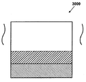
- 238000010586 diagram Methods 0.000 description 14
- 229910045601 alloy Inorganic materials 0.000 description 13
- 239000000377 silicon dioxide Substances 0.000 description 13
- 239000012071 phase Substances 0.000 description 12
- 238000000137 annealing Methods 0.000 description 11
- 230000008901 benefit Effects 0.000 description 11
- 238000005137 deposition process Methods 0.000 description 11
- 230000000694 effects Effects 0.000 description 11
- 238000004050 hot filament vapor deposition Methods 0.000 description 11
- 238000007654 immersion Methods 0.000 description 11
- 238000011065 in-situ storage Methods 0.000 description 11
- 230000005670 electromagnetic radiation Effects 0.000 description 10
- 239000002241 glass-ceramic Substances 0.000 description 10
- BASFCYQUMIYNBI-UHFFFAOYSA-N platinum Chemical compound [Pt] BASFCYQUMIYNBI-UHFFFAOYSA-N 0.000 description 10
- 230000008859 change Effects 0.000 description 9
- 239000004020 conductor Substances 0.000 description 9
- 238000002360 preparation method Methods 0.000 description 9
- 238000000926 separation method Methods 0.000 description 9
- 150000001875 compounds Chemical class 0.000 description 8
- 230000006870 function Effects 0.000 description 8
- 239000001307 helium Substances 0.000 description 8
- 229910052734 helium Inorganic materials 0.000 description 8
- SWQJXJOGLNCZEY-UHFFFAOYSA-N helium atom Chemical compound [He] SWQJXJOGLNCZEY-UHFFFAOYSA-N 0.000 description 8
- 238000005468 ion implantation Methods 0.000 description 8
- 239000007788 liquid Substances 0.000 description 8
- VNWKTOKETHGBQD-UHFFFAOYSA-N methane Chemical compound C VNWKTOKETHGBQD-UHFFFAOYSA-N 0.000 description 8
- 230000007935 neutral effect Effects 0.000 description 8
- JBRZTFJDHDCESZ-UHFFFAOYSA-N AsGa Chemical compound [As]#[Ga] JBRZTFJDHDCESZ-UHFFFAOYSA-N 0.000 description 7
- 229910001218 Gallium arsenide Inorganic materials 0.000 description 7
- 239000012790 adhesive layer Substances 0.000 description 7
- 239000002105 nanoparticle Substances 0.000 description 7
- 229920005591 polysilicon Polymers 0.000 description 7
- 239000002344 surface layer Substances 0.000 description 7
- 239000000853 adhesive Substances 0.000 description 6
- 230000001070 adhesive effect Effects 0.000 description 6
- 229910052782 aluminium Inorganic materials 0.000 description 6
- XAGFODPZIPBFFR-UHFFFAOYSA-N aluminium Chemical compound [Al] XAGFODPZIPBFFR-UHFFFAOYSA-N 0.000 description 6
- 238000010884 ion-beam technique Methods 0.000 description 6
- 229910052751 metal Inorganic materials 0.000 description 6
- 239000002184 metal Substances 0.000 description 6
- 230000008719 thickening Effects 0.000 description 6
- RTAQQCXQSZGOHL-UHFFFAOYSA-N Titanium Chemical compound [Ti] RTAQQCXQSZGOHL-UHFFFAOYSA-N 0.000 description 5
- 238000010790 dilution Methods 0.000 description 5
- 239000012895 dilution Substances 0.000 description 5
- 230000009977 dual effect Effects 0.000 description 5
- 238000002347 injection Methods 0.000 description 5
- 239000007924 injection Substances 0.000 description 5
- 229910052697 platinum Inorganic materials 0.000 description 5
- 229910052719 titanium Inorganic materials 0.000 description 5
- 239000010936 titanium Substances 0.000 description 5
- WFKWXMTUELFFGS-UHFFFAOYSA-N tungsten Chemical compound [W] WFKWXMTUELFFGS-UHFFFAOYSA-N 0.000 description 5
- 229910052721 tungsten Inorganic materials 0.000 description 5
- 239000010937 tungsten Substances 0.000 description 5
- IJGRMHOSHXDMSA-UHFFFAOYSA-N Atomic nitrogen Chemical compound N#N IJGRMHOSHXDMSA-UHFFFAOYSA-N 0.000 description 4
- 239000005046 Chlorosilane Substances 0.000 description 4
- KOPOQZFJUQMUML-UHFFFAOYSA-N chlorosilane Chemical class Cl[SiH3] KOPOQZFJUQMUML-UHFFFAOYSA-N 0.000 description 4
- 239000011248 coating agent Substances 0.000 description 4
- 238000000576 coating method Methods 0.000 description 4
- 239000002131 composite material Substances 0.000 description 4
- 238000001035 drying Methods 0.000 description 4
- 150000002431 hydrogen Chemical class 0.000 description 4
- 150000002483 hydrogen compounds Chemical class 0.000 description 4
- 230000002427 irreversible effect Effects 0.000 description 4
- 238000005224 laser annealing Methods 0.000 description 4
- 239000005543 nano-size silicon particle Substances 0.000 description 4
- 229910052754 neon Inorganic materials 0.000 description 4
- GKAOGPIIYCISHV-UHFFFAOYSA-N neon atom Chemical compound [Ne] GKAOGPIIYCISHV-UHFFFAOYSA-N 0.000 description 4
- 229910052756 noble gas Inorganic materials 0.000 description 4
- 238000010899 nucleation Methods 0.000 description 4
- 230000006911 nucleation Effects 0.000 description 4
- 238000004806 packaging method and process Methods 0.000 description 4
- 238000005240 physical vapour deposition Methods 0.000 description 4
- 229920000642 polymer Polymers 0.000 description 4
- 230000005855 radiation Effects 0.000 description 4
- 238000004151 rapid thermal annealing Methods 0.000 description 4
- 238000001228 spectrum Methods 0.000 description 4
- XLYOFNOQVPJJNP-UHFFFAOYSA-N water Chemical compound O XLYOFNOQVPJJNP-UHFFFAOYSA-N 0.000 description 4
- 229910003902 SiCl 4 Inorganic materials 0.000 description 3
- 238000001505 atmospheric-pressure chemical vapour deposition Methods 0.000 description 3
- QVGXLLKOCUKJST-UHFFFAOYSA-N atomic oxygen Chemical compound [O] QVGXLLKOCUKJST-UHFFFAOYSA-N 0.000 description 3
- 230000015556 catabolic process Effects 0.000 description 3
- 239000006059 cover glass Substances 0.000 description 3
- 238000001514 detection method Methods 0.000 description 3
- 238000009792 diffusion process Methods 0.000 description 3
- 230000031700 light absorption Effects 0.000 description 3
- 239000007791 liquid phase Substances 0.000 description 3
- 238000004518 low pressure chemical vapour deposition Methods 0.000 description 3
- 238000005259 measurement Methods 0.000 description 3
- 239000000203 mixture Substances 0.000 description 3
- QJGQUHMNIGDVPM-UHFFFAOYSA-N nitrogen group Chemical group [N] QJGQUHMNIGDVPM-UHFFFAOYSA-N 0.000 description 3
- 239000001301 oxygen Substances 0.000 description 3
- 229910052760 oxygen Inorganic materials 0.000 description 3
- 230000036961 partial effect Effects 0.000 description 3
- 239000003208 petroleum Substances 0.000 description 3
- 230000001699 photocatalysis Effects 0.000 description 3
- 229910021426 porous silicon Inorganic materials 0.000 description 3
- 230000001902 propagating effect Effects 0.000 description 3
- 239000000243 solution Substances 0.000 description 3
- MHAJPDPJQMAIIY-UHFFFAOYSA-N Hydrogen peroxide Chemical compound OO MHAJPDPJQMAIIY-UHFFFAOYSA-N 0.000 description 2
- XYFCBTPGUUZFHI-UHFFFAOYSA-N Phosphine Chemical compound P XYFCBTPGUUZFHI-UHFFFAOYSA-N 0.000 description 2
- QAOWNCQODCNURD-UHFFFAOYSA-N Sulfuric acid Chemical compound OS(O)(=O)=O QAOWNCQODCNURD-UHFFFAOYSA-N 0.000 description 2
- 238000000995 aerosol-assisted chemical vapour deposition Methods 0.000 description 2
- 238000000277 atomic layer chemical vapour deposition Methods 0.000 description 2
- 238000000231 atomic layer deposition Methods 0.000 description 2
- 230000005540 biological transmission Effects 0.000 description 2
- 239000002178 crystalline material Substances 0.000 description 2
- 230000002950 deficient Effects 0.000 description 2
- 238000013461 design Methods 0.000 description 2
- 239000003085 diluting agent Substances 0.000 description 2
- 238000001928 direct liquid injection chemical vapour deposition Methods 0.000 description 2
- 238000009826 distribution Methods 0.000 description 2
- 238000011066 ex-situ storage Methods 0.000 description 2
- 230000005284 excitation Effects 0.000 description 2
- 230000009975 flexible effect Effects 0.000 description 2
- 239000005329 float glass Substances 0.000 description 2
- 238000005286 illumination Methods 0.000 description 2
- 230000001678 irradiating effect Effects 0.000 description 2
- 239000002648 laminated material Substances 0.000 description 2
- 239000007769 metal material Substances 0.000 description 2
- 238000000259 microwave plasma-assisted chemical vapour deposition Methods 0.000 description 2
- 230000003647 oxidation Effects 0.000 description 2
- 238000007254 oxidation reaction Methods 0.000 description 2
- 239000005022 packaging material Substances 0.000 description 2
- 230000000737 periodic effect Effects 0.000 description 2
- 230000002093 peripheral effect Effects 0.000 description 2
- 238000005498 polishing Methods 0.000 description 2
- 239000002861 polymer material Substances 0.000 description 2
- 238000005086 pumping Methods 0.000 description 2
- 238000001289 rapid thermal chemical vapour deposition Methods 0.000 description 2
- 238000001953 recrystallisation Methods 0.000 description 2
- 230000002829 reductive effect Effects 0.000 description 2
- 238000000663 remote plasma-enhanced chemical vapour deposition Methods 0.000 description 2
- HBMJWWWQQXIZIP-UHFFFAOYSA-N silicon carbide Chemical compound [Si+]#[C-] HBMJWWWQQXIZIP-UHFFFAOYSA-N 0.000 description 2
- 229910010271 silicon carbide Inorganic materials 0.000 description 2
- 238000005507 spraying Methods 0.000 description 2
- WGTYBPLFGIVFAS-UHFFFAOYSA-M tetramethylammonium hydroxide Chemical compound [OH-].C[N+](C)(C)C WGTYBPLFGIVFAS-UHFFFAOYSA-M 0.000 description 2
- 239000002759 woven fabric Substances 0.000 description 2
- OKTJSMMVPCPJKN-UHFFFAOYSA-N Carbon Chemical compound [C] OKTJSMMVPCPJKN-UHFFFAOYSA-N 0.000 description 1
- 239000004593 Epoxy Substances 0.000 description 1
- KRHYYFGTRYWZRS-UHFFFAOYSA-N Fluorane Chemical compound F KRHYYFGTRYWZRS-UHFFFAOYSA-N 0.000 description 1
- JMASRVWKEDWRBT-UHFFFAOYSA-N Gallium nitride Chemical compound [Ga]#N JMASRVWKEDWRBT-UHFFFAOYSA-N 0.000 description 1
- 208000012766 Growth delay Diseases 0.000 description 1
- VEXZGXHMUGYJMC-UHFFFAOYSA-N Hydrochloric acid Chemical compound Cl VEXZGXHMUGYJMC-UHFFFAOYSA-N 0.000 description 1
- 239000004642 Polyimide Substances 0.000 description 1
- BQCADISMDOOEFD-UHFFFAOYSA-N Silver Chemical compound [Ag] BQCADISMDOOEFD-UHFFFAOYSA-N 0.000 description 1
- 239000006096 absorbing agent Substances 0.000 description 1
- 238000010521 absorption reaction Methods 0.000 description 1
- 238000001994 activation Methods 0.000 description 1
- 239000005456 alcohol based solvent Substances 0.000 description 1
- 230000003698 anagen phase Effects 0.000 description 1
- 239000012298 atmosphere Substances 0.000 description 1
- 238000003877 atomic layer epitaxy Methods 0.000 description 1
- 230000002238 attenuated effect Effects 0.000 description 1
- 238000010923 batch production Methods 0.000 description 1
- 229910052799 carbon Inorganic materials 0.000 description 1
- 239000000969 carrier Substances 0.000 description 1
- 230000002925 chemical effect Effects 0.000 description 1
- 238000012993 chemical processing Methods 0.000 description 1
- 238000005253 cladding Methods 0.000 description 1
- 239000003245 coal Substances 0.000 description 1
- 230000002301 combined effect Effects 0.000 description 1
- 230000002860 competitive effect Effects 0.000 description 1
- 238000010276 construction Methods 0.000 description 1
- 238000011109 contamination Methods 0.000 description 1
- 230000032798 delamination Effects 0.000 description 1
- 230000003111 delayed effect Effects 0.000 description 1
- 239000006185 dispersion Substances 0.000 description 1
- 230000005611 electricity Effects 0.000 description 1
- PCHJSUWPFVWCPO-UHFFFAOYSA-N gold Chemical compound [Au] PCHJSUWPFVWCPO-UHFFFAOYSA-N 0.000 description 1
- 229910052737 gold Inorganic materials 0.000 description 1
- 239000010931 gold Substances 0.000 description 1
- 229910000041 hydrogen chloride Inorganic materials 0.000 description 1
- IXCSERBJSXMMFS-UHFFFAOYSA-N hydrogen chloride Substances Cl.Cl IXCSERBJSXMMFS-UHFFFAOYSA-N 0.000 description 1
- 229910000040 hydrogen fluoride Inorganic materials 0.000 description 1
- 239000007943 implant Substances 0.000 description 1
- 238000009616 inductively coupled plasma Methods 0.000 description 1
- 239000011261 inert gas Substances 0.000 description 1
- 238000007641 inkjet printing Methods 0.000 description 1
- 230000000670 limiting effect Effects 0.000 description 1
- 230000005923 long-lasting effect Effects 0.000 description 1
- 239000003921 oil Substances 0.000 description 1
- 229910000073 phosphorus hydride Inorganic materials 0.000 description 1
- 230000000704 physical effect Effects 0.000 description 1
- 230000010287 polarization Effects 0.000 description 1
- 229920000548 poly(silane) polymer Polymers 0.000 description 1
- 229920001721 polyimide Polymers 0.000 description 1
- 238000010248 power generation Methods 0.000 description 1
- 230000009290 primary effect Effects 0.000 description 1
- 238000010926 purge Methods 0.000 description 1
- 239000012495 reaction gas Substances 0.000 description 1
- 230000008707 rearrangement Effects 0.000 description 1
- 238000002310 reflectometry Methods 0.000 description 1
- 238000011160 research Methods 0.000 description 1
- 239000013557 residual solvent Substances 0.000 description 1
- 238000007650 screen-printing Methods 0.000 description 1
- 125000005624 silicic acid group Chemical class 0.000 description 1
- 229910052709 silver Inorganic materials 0.000 description 1
- 239000004332 silver Substances 0.000 description 1
- 239000007921 spray Substances 0.000 description 1
- 239000007858 starting material Substances 0.000 description 1
- 239000000126 substance Substances 0.000 description 1
- 238000004381 surface treatment Methods 0.000 description 1
- 230000005469 synchrotron radiation Effects 0.000 description 1
- 238000000038 ultrahigh vacuum chemical vapour deposition Methods 0.000 description 1
- 238000005019 vapor deposition process Methods 0.000 description 1
- 238000001429 visible spectrum Methods 0.000 description 1
- 230000003313 weakening effect Effects 0.000 description 1
Images


Classifications
-
- H—ELECTRICITY
- H10—SEMICONDUCTOR DEVICES; ELECTRIC SOLID-STATE DEVICES NOT OTHERWISE PROVIDED FOR
- H10F—INORGANIC SEMICONDUCTOR DEVICES SENSITIVE TO INFRARED RADIATION, LIGHT, ELECTROMAGNETIC RADIATION OF SHORTER WAVELENGTH OR CORPUSCULAR RADIATION
- H10F71/00—Manufacture or treatment of devices covered by this subclass
- H10F71/121—The active layers comprising only Group IV materials
-
- H—ELECTRICITY
- H10—SEMICONDUCTOR DEVICES; ELECTRIC SOLID-STATE DEVICES NOT OTHERWISE PROVIDED FOR
- H10F—INORGANIC SEMICONDUCTOR DEVICES SENSITIVE TO INFRARED RADIATION, LIGHT, ELECTROMAGNETIC RADIATION OF SHORTER WAVELENGTH OR CORPUSCULAR RADIATION
- H10F10/00—Individual photovoltaic cells, e.g. solar cells
- H10F10/10—Individual photovoltaic cells, e.g. solar cells having potential barriers
- H10F10/16—Photovoltaic cells having only PN heterojunction potential barriers
- H10F10/161—Photovoltaic cells having only PN heterojunction potential barriers comprising multiple PN heterojunctions, e.g. tandem cells
-
- H—ELECTRICITY
- H10—SEMICONDUCTOR DEVICES; ELECTRIC SOLID-STATE DEVICES NOT OTHERWISE PROVIDED FOR
- H10F—INORGANIC SEMICONDUCTOR DEVICES SENSITIVE TO INFRARED RADIATION, LIGHT, ELECTROMAGNETIC RADIATION OF SHORTER WAVELENGTH OR CORPUSCULAR RADIATION
- H10F10/00—Individual photovoltaic cells, e.g. solar cells
- H10F10/10—Individual photovoltaic cells, e.g. solar cells having potential barriers
- H10F10/16—Photovoltaic cells having only PN heterojunction potential barriers
- H10F10/164—Photovoltaic cells having only PN heterojunction potential barriers comprising heterojunctions with Group IV materials, e.g. ITO/Si or GaAs/SiGe photovoltaic cells
- H10F10/165—Photovoltaic cells having only PN heterojunction potential barriers comprising heterojunctions with Group IV materials, e.g. ITO/Si or GaAs/SiGe photovoltaic cells the heterojunctions being Group IV-IV heterojunctions, e.g. Si/Ge, SiGe/Si or Si/SiC photovoltaic cells
-
- H—ELECTRICITY
- H10—SEMICONDUCTOR DEVICES; ELECTRIC SOLID-STATE DEVICES NOT OTHERWISE PROVIDED FOR
- H10F—INORGANIC SEMICONDUCTOR DEVICES SENSITIVE TO INFRARED RADIATION, LIGHT, ELECTROMAGNETIC RADIATION OF SHORTER WAVELENGTH OR CORPUSCULAR RADIATION
- H10F10/00—Individual photovoltaic cells, e.g. solar cells
- H10F10/10—Individual photovoltaic cells, e.g. solar cells having potential barriers
- H10F10/17—Photovoltaic cells having only PIN junction potential barriers
- H10F10/174—Photovoltaic cells having only PIN junction potential barriers comprising monocrystalline or polycrystalline materials
-
- H—ELECTRICITY
- H10—SEMICONDUCTOR DEVICES; ELECTRIC SOLID-STATE DEVICES NOT OTHERWISE PROVIDED FOR
- H10F—INORGANIC SEMICONDUCTOR DEVICES SENSITIVE TO INFRARED RADIATION, LIGHT, ELECTROMAGNETIC RADIATION OF SHORTER WAVELENGTH OR CORPUSCULAR RADIATION
- H10F71/00—Manufacture or treatment of devices covered by this subclass
- H10F71/131—Recrystallisation; Crystallization of amorphous or microcrystalline semiconductors
-
- H—ELECTRICITY
- H10—SEMICONDUCTOR DEVICES; ELECTRIC SOLID-STATE DEVICES NOT OTHERWISE PROVIDED FOR
- H10F—INORGANIC SEMICONDUCTOR DEVICES SENSITIVE TO INFRARED RADIATION, LIGHT, ELECTROMAGNETIC RADIATION OF SHORTER WAVELENGTH OR CORPUSCULAR RADIATION
- H10F71/00—Manufacture or treatment of devices covered by this subclass
- H10F71/139—Manufacture or treatment of devices covered by this subclass using temporary substrates
-
- H—ELECTRICITY
- H10—SEMICONDUCTOR DEVICES; ELECTRIC SOLID-STATE DEVICES NOT OTHERWISE PROVIDED FOR
- H10F—INORGANIC SEMICONDUCTOR DEVICES SENSITIVE TO INFRARED RADIATION, LIGHT, ELECTROMAGNETIC RADIATION OF SHORTER WAVELENGTH OR CORPUSCULAR RADIATION
- H10F77/00—Constructional details of devices covered by this subclass
- H10F77/10—Semiconductor bodies
- H10F77/16—Material structures, e.g. crystalline structures, film structures or crystal plane orientations
- H10F77/169—Thin semiconductor films on metallic or insulating substrates
- H10F77/1696—Thin semiconductor films on metallic or insulating substrates the films including Group II-VI materials, e.g. CdTe or CdS
-
- H—ELECTRICITY
- H10—SEMICONDUCTOR DEVICES; ELECTRIC SOLID-STATE DEVICES NOT OTHERWISE PROVIDED FOR
- H10F—INORGANIC SEMICONDUCTOR DEVICES SENSITIVE TO INFRARED RADIATION, LIGHT, ELECTROMAGNETIC RADIATION OF SHORTER WAVELENGTH OR CORPUSCULAR RADIATION
- H10F77/00—Constructional details of devices covered by this subclass
- H10F77/40—Optical elements or arrangements
-
- Y—GENERAL TAGGING OF NEW TECHNOLOGICAL DEVELOPMENTS; GENERAL TAGGING OF CROSS-SECTIONAL TECHNOLOGIES SPANNING OVER SEVERAL SECTIONS OF THE IPC; TECHNICAL SUBJECTS COVERED BY FORMER USPC CROSS-REFERENCE ART COLLECTIONS [XRACs] AND DIGESTS
- Y02—TECHNOLOGIES OR APPLICATIONS FOR MITIGATION OR ADAPTATION AGAINST CLIMATE CHANGE
- Y02E—REDUCTION OF GREENHOUSE GAS [GHG] EMISSIONS, RELATED TO ENERGY GENERATION, TRANSMISSION OR DISTRIBUTION
- Y02E10/00—Energy generation through renewable energy sources
- Y02E10/50—Photovoltaic [PV] energy
- Y02E10/547—Monocrystalline silicon PV cells
-
- Y—GENERAL TAGGING OF NEW TECHNOLOGICAL DEVELOPMENTS; GENERAL TAGGING OF CROSS-SECTIONAL TECHNOLOGIES SPANNING OVER SEVERAL SECTIONS OF THE IPC; TECHNICAL SUBJECTS COVERED BY FORMER USPC CROSS-REFERENCE ART COLLECTIONS [XRACs] AND DIGESTS
- Y02—TECHNOLOGIES OR APPLICATIONS FOR MITIGATION OR ADAPTATION AGAINST CLIMATE CHANGE
- Y02P—CLIMATE CHANGE MITIGATION TECHNOLOGIES IN THE PRODUCTION OR PROCESSING OF GOODS
- Y02P70/00—Climate change mitigation technologies in the production process for final industrial or consumer products
- Y02P70/50—Manufacturing or production processes characterised by the final manufactured product
Description
本特許出願は、下記の米国仮特許出願、つまり2006年3月17日の仮特許出願第60/783,586号、2006年8月15日の仮特許出願第60/822,473号、2006年8月23日の仮特許出願第60/823,354および2006年8月23日の仮特許出願60/823,356号に基づく優先権を主張するものであり、これらの米国仮特許出願の全ては、全ての目的において参照されて、本特許出願に包含される。
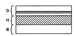
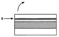
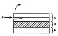
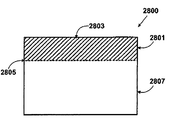
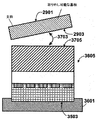
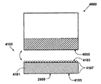
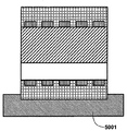
(1)半導体基板を形成する。半導体基板は、表面部、劈開部および前記表面部と前記劈開部の間にあって、除去される第1の材料層を有する。
(2)光学透明性基板に半導体基板を配置する。
(3)光学透明性基板の第1の表面部に半導体基板の表面部を結合する。
(4)劈開部の一部で、制御された劈開動作を開始する。
(5)半導体基板から第1の材料層を除去するため、半導体基板を劈開する。一方、劈開表面部の形成を促すために、前記表面部は、前記第1の表面部に結合されたままとなっている。
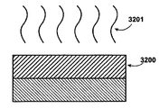
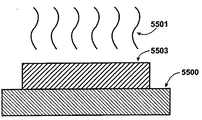
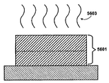
(6)半導体材料の生成層を形成するために、(例えば、シラン種を用いて)劈開表面部の上を覆って、第2の半導体材料層を形成する。半導体材料の生成層は、1または複数の光電子部を有する。
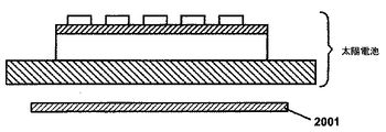
(7)第2の半導体材料層の上を覆って、カバーガラス材料を取り付ける。
(8)必要に応じて、その他のステップを実行する。
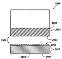
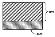
(1)シリコン、ゲルマニウム、シリコン−ゲルマニウム合金、ヒ化ガリウム、あらゆるIII/V族化合物およびその他の材料などの半導体基板を形成する(ステップ2701)。
(2)第1のシリコン材料層を定めるために(ステップ2705)、劈開平面(複数の粒子、蒸着物質、またはこれらの任意の組み合わせなどを含んでいる)を形成する(ステップ2703)。
(3)第1の材料層をシリコン支持部材の上を覆う脱着可能な材料に転写する(ステップ2707)。
(4)前記脱着可能な材料の上を覆う全材料層を形成するために、前記第1の材料層の上を覆う第2の材料層を形成する(ステップ2709)。
(5)全材料層の第1の部分(例えば、第1の端面)に、第1の光電子セル表面を形成する(ステップ2711)。
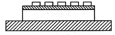
(6)前記第1の光電子セル表面の上を覆う表面部を形成する。
(7)キャリア部材を第1の光電子セル表面の表面部に取り付ける(ステップ2713)。
(7)全材料層の第2の部分を露出するため、脱着可能な材料を含むシリコン支持部材を除去する(ステップ2715)。
(8)全材料層の第2の部分で、第2の光電子セル表面を形成する(ステップ2717)。
(9)他のプロセスを実行する(ステップ2719)。
(10)ソーラーモジュールを形成する(ステップ2721)。
(11)停止。
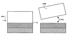
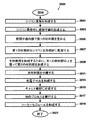
(1)表面部、底部、および材料の所定の層を有する半導体基板を形成する(ステップ3901)。前記半導体基板は、シリコン、ゲルマニウム、シリコン−ゲルマニウム合金、ヒ化ガリウム、あらゆるIII/V材料などであってもよい。
(2)第1のシリコン材料層を定めるために(ステップ3905)、劈開平面を形成する(複数の粒子、蒸着物質、またはこれらのあらゆる組み合わせなどを含む(ステップ3903)。
(3)第1の材料層をシリコン支持部材の上を覆う脱着可能な材料に転写する(ステップ3907)。
(4)前記脱着可能な材料の上を覆う全材料層を形成するために、前記第1の材料層の上を覆う第2の材料層を形成する(ステップ3909)。
(5)前記全材料層を除去する(ステップ3911)。
(6)前記全材料層の一部に光電子セル表面を形成する(ステップ3913)。
(7)光電子セルを含む前記全材料層をキャリア部材に付着する(ステップ3915)。(8)他のプロセスを実行する(ステップ3917)。
(9)ソーラーモジュールを形成する(ステップ3919)。
(10)終了。
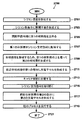
(1)シリコン、ゲルマニウム、シリコン−ゲルマニウム合金、ヒ化ガリウム、あらゆるIII/V材料などの半導体基板を形成する(ステップ5101)。
(2)第1のシリコン材料層を定めるために(ステップ5105)、劈開平面を形成する(ステップ5103)。
(3)第1の材料層をキャリア部材基板に転写する(ステップ5107)。
(4)全材料厚さを形成するために、第1の半導体材料層の上を覆う第2の材料層を形成する(ステップ5109)。
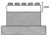
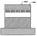
(5)前記全材料層の一面に第1の光電子セル表面を少なくとも1つ形成する(ステップ5111)。
(6)望ましいように、他のプロセスを実行する(ステップ5113)。
(7)終了(ステップ5115)。
Claims (37)
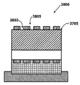
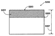
- 表面部、劈開部および、前記表面部と前記劈開部との間にあって、除去される第1の材料層を有する半導体基板を形成する工程と、
前記半導体基板の前記表面部を、第1の表面部および第2の表面部を有する光学透明性基板の前記第1の表面部に結合する工程と、
前記表面部を前記第1の表面部に結合したままで、前記半導体基板を劈開して、前記第1の材料層を前記半導体基板から除去して、劈開表面部を形成する工程と、さらに、
前記劈開表面部の上をアモルファスシリコンで形成された第2の半導体材料層で覆う工程と、
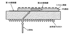
前記光学透明性基板の前記第2の表面部に、光線を前記光学透明性基板に対して斜めに入射させる光学素子を結合する工程と、からなる
ことを特徴とする光電子セルの製造方法。 - さらに、アモルファスシリコン層の結晶化を含む
ことを特徴とする請求項1に記載の光電子セルの製造方法。 - 第1の表面および第2の表面からなる光学透明性基板と、
前記光学透明性基板の第1の表面の上を覆う第1の表面部および第2の表面部を有する第1の材料層と、
前記材料層の第1の表面部と光学透明性材料の第1の表面との間に担持される光結合材料と、
半導体材料の生成層を形成するために、前記第2の表面部の上を覆うアモルファスシリコンからなる第2の半導体材料層と、
前記光学透明性基板の前記第2の表面部を覆って、光線を前記光学透明性基板に対して斜めに入射させる光学素子と、を備える
ことを特徴とする光電子セル装置。 - 前記光結合材料は、酸化スズ、インジウム−スズ酸化物、酸化亜鉛または二酸化チタンを含んでなる
ことを特徴とする請求項3に記載の光電子セル装置。 - 前記第1の半導体材料層は、単結晶シリコン材料を含んでなる
ことを特徴とする請求項3に記載の光電子セル装置。 - 前記光学透明性材料は、ガラス基板、石英基板またはプラスチック基板を含んでなる
ことを特徴とする請求項3に記載の光電子セル装置。 - さらに、前記第2の半導体材料層の上を覆う裏面カバーを含んでなる
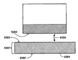
ことを特徴とする請求項3に記載の光電子セル装置。 - 劈開部と、表面部と、前記劈開部と前記表面部との間で定められる第1のシリコン材料層と、を備えるドナー基板を形成する工程と、
前記劈開部の周辺の内側で前記ドナー基板の一部を分離するため、および前記第1のシリコン材料層の上を覆う劈開表面部の形成を促すように処理基板の処理基板表面に前記表面部を結合するために、前記第1のシリコン材料層を前記処理基板の処理基板表面に転写する工程と、
反応室にシラン種を含むガスを供給する工程と、
グロー放電CVD法、プラズマCVD法、光CVD法または熱CVD法を含む1または複数のプロセスから選ばれるプロセスを用いて、前記反応室内部にある前記処理基板の前記処理基板表面部にシリコン蒸着状態を促すように、前記シラン種を用いる工程と、
前記第1のシリコン材料の上を覆う前記シラン種を用いて、アモルファスシリコンからなる第2の材料層を形成する工程と、
前記ドナー基板を、第1の表面部および第2の表面部を有する光学透明性基板の前記第1の表面部に結合する工程と、
前記光学透明性基板の前記第2の表面部に、光線を前記光学透明性基板に対して斜めに入射させる光学素子を結合する工程と、を有する
ことを特徴とする光電子セル装置の製造方法。 - 前記第2の材料層を形成する温度は、約650℃以下の範囲にある温度に維持される
ことを特徴とする請求項8に記載の光電子セル装置の製造方法。 - さらに、前記第2の材料層の厚さをより増加するために、供給、使用、形成、および処理プロセスを繰り返す工程を有する
ことを特徴とする請求項8に記載の光電子セル装置の製造方法。 - さらに、洗浄プロセスに前記劈開表面部を曝す工程を有する
ことを特徴とする請求項8に記載の光電子セル装置の製造方法。 - 前記洗浄プロセスは、プラズマへの曝露を含む
ことを特徴とする請求項11に記載の光電子セル装置の製造方法。 - 前記洗浄プロセスは、湿式洗浄プロセスへの曝露を含む
ことを特徴とする請求項11に記載の光電子セル装置の製造方法。 - 劈開部と、表面部と、前記劈開部と前記表面部との間で定められる第1のシリコンあるいはゲルマニウム材料層を有するドナー基板を形成する工程と、
前記第1のシリコンあるいはゲルマニウム材料層の上を覆う劈開表面部の形成を促すように、前記劈開部の周辺の内側で前記ドナー基板の一部を分離するため、および処理基板の処理基板表面部に前記表面部を結合するために、前記第1のシリコンあるいはゲルマニウム材料層を前記処理基板の処理基板表面部に転写する工程と、
反応室にシランおよび/またはゲルマン種を含むガスを供給する工程と、
少なくともグロー放電CVD、プラズマCVD、光CVDまたは熱CVDから選択されるプロセスおよびシランおよび/またはゲルマン種を用いて、前記第1のシリコンまたはゲルマニウム材料層の上を覆う材料を結晶化するための材料の固相エピタキシャル再成長速度と等しいか、より速いか、またはより遅い蒸着速度で前記第1のシリコンまたはゲルマニウム材料層を厚くするために、前記劈開表面の上を覆って材料を蒸着してアモルファスシリコン層を形成する工程と、
前記ドナー基板を、第1の表面部および第2の表面部を有する光学透明性基板の前記第1の表面部に結合する工程と、
前記光学透明性基板の前記第2の表面部に、光線を前記光学透明性基板に対して斜めに入射させる光学素子を結合する工程と、からなる
ことを特徴とする光電子セル装置の製造方法。 - 前記材料の蒸着は、約650℃以下の温度で生じる
ことを特徴とする請求項14に記載の光電子セル装置の製造方法。 - さらに、前記材料の蒸着前に、グラフォエピタキシーによってシード層を形成する工程を有する
ことを特徴とする請求項14に記載の光電子セル装置の製造方法。 - 前記シラン種は、トリシラン、ジシラン、ジクロロシラン、トリクロロシランまたはモノシランを含む
ことを特徴とする請求項14に記載の光電子セル装置の製造方法。 - 前記ゲルマン種は、ゲルマン(GeH4)またはジゲルマン(Ge2H6)を含む
ことを特徴とする請求項14に記載の光電子セル装置の製造方法。 - PおよびN接合部を形成するために、前記シランおよび/またはゲルマン種の蒸着は、1または複数のドーパントガスを含む
ことを特徴とする請求項14に記載の光電子セル装置の製造方法。 - さらに、前記処理基板表面部および前記処理基板の裏面部に第1の光電子部を形成し、
そして、前記処理基板表面部には第1の光電子材料を、前記処理基板の裏面には第2の光電子材料をそれぞれ形成するために、前記処理基板の裏面部に、第2のシリコン材料を同時蒸着する工程を含む
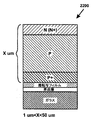
ことを特徴とする請求項14に記載の光電子セル装置の製造方法。 - 処理基板表面部を有する処理基板と、
前記処理基板表面部の上を覆う界面材料と、
前記界面材料の上を覆う層転写フィルムと、
1または複数の欠陥を有する単結晶シリコンまたは単結晶ゲルマニウム材料からなる第1の蒸着層と、
前記第1の蒸着層を覆うアモルファスシリコンからなる第2の蒸着層と、を備えるとともに、
前記処理基板は光学透明性基板であって、
前記光学透明性基板の前記界面材料で覆われた表面の反対側の表面を覆って、光線を前記光学透明性基板に対して斜めに入射させる光学素子を備える
ことを特徴とする光電子装置。 - 前記単結晶シリコンまたは単結晶ゲルマニウムの蒸着層は、前記層転写フィルムの上を覆うP型材料および前記P型材料の上を覆うN型材料を有する
ことを特徴とする請求項21に記載の光電子装置。 - 前記P型材料は、P+型材料を含む
ことを特徴とする請求項22に記載の光電子装置。 - 前記単結晶シリコンまたは単結晶ゲルマニウムの蒸着層は、前記層転写フィルムの上を覆うN型材料および前記N型材料の上を覆うP型材料を有する
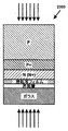
ことを特徴とする請求項21に記載の光電子装置。 - 表面部、底部および前記表面部と前記底部との間に所定の層を有する支持部材を形成する工程と、
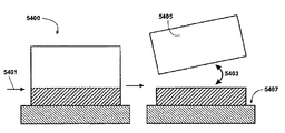
前記支持部材の表面部の上を覆う脱着可能な材料を形成する工程と、
前記支持部材の上を覆う前記脱着可能な材料の上を覆う第1の転写材料層を形成するために、第1の半導体材料層を前記脱着可能な材料の上を覆う第1のドナー基板から転写する工程と、
前記脱着可能な材料の上を覆う全材料層を形成するために、前記第1の転写材料層の上を覆うアモルファスシリコンからなる第2の半導体材料層を形成する工程と、
前記脱着可能な材料から前記全材料層を分離するために、前記脱着可能な材料から前記全材料層を切り離す工程と、
前記全材料層の1または複数の部分に1または複数の光電子装置を形成する工程と、からなるとともに、
前記支持部材は、光学透明性基板であって、
前記光学透明性基板の前記底部に、光線を前記光学透明性基板に対して斜めに入射させる光学素子を結合する工程をさらに有する
ことを特徴とする1または複数のソーラーモジュールに用いられる太陽電池の製造方法。 - 前記支持部材は、第1のドナー基板が有する第2の熱膨張係数と実質的に一致する第1の熱膨張係数を有する
ことを特徴とする請求項25に記載のソーラーモジュールに用いられる太陽電池の製造方法。 - 前記表面部は、表面粗さと上面を覆う酸化物層を有する
ことを特徴とする請求項25に記載のソーラーモジュールに用いられる太陽電池の製造方法。 - 前記表面粗さは、少なくとも多孔性材料によって実現される
ことを特徴とする請求項27に記載のソーラーモジュールに用いられる太陽電池の製造方法。 - 前記シリコン支持部材は、前記支持部材の底部から前記支持部材層を通って、前記表面部の一部に向かって広がる開口部を有するとともに、前記開口部は流体駆動源に結合され、
前記流体駆動源は、前記底部と前記表面部の一部との間で、前記開口部の内部に圧力勾配を誘発できる
ことを特徴とする請求項25に記載のソーラーモジュールに用いられる太陽電池の製造方法。 - 前記圧力勾配は、流体によって提供され、前記脱着可能な材料からの前記全材料層の除去を容易にする
ことを特徴とする請求項29に記載のソーラーモジュールに用いられる太陽電池の製造方法。 - 前記流体は、前記脱着可能な材料に対するエッチング液である
ことを特徴とする請求項30に記載のソーラーモジュールに用いられる太陽電池の製造方法。 - 劈開工程は、前記脱着可能な材料の一部から全層の一部を除去する開始プロセスと、前記脱着可能な材料から前記全層を分離し続ける伝播プロセスと、を有する
ことを特徴とする請求項25に記載のソーラーモジュールに用いられる太陽電池の製造方法。 - 前記第2の層を形成する工程は、エピタキシャルシリコン材料を蒸着する工程を含む
ことを特徴とする請求項25に記載のソーラーモジュールに用いられる太陽電池の製造方法。 - シリコン支持部材は再利用できる
ことを特徴とする請求項25に記載のソーラーモジュールに用いられる太陽電池の製造方法。 - 前記脱着可能な材料は、表面粗さおよび上面を覆う誘電材料を備える
ことを特徴とする請求項25に記載のソーラーモジュールに用いられる太陽電池の製造方法。 - さらに、1または複数の光電子材料を全材料層の1または複数の部分に形成する工程を含んでなる
ことを特徴とする請求項25に記載のソーラーモジュールに用いられる太陽電池の製造方法。 - 前記全層は、200ミクロン以下の寸法である
ことを特徴とする請求項25に記載のソーラーモジュールに用いられる太陽電池の製造方法。
Applications Claiming Priority (9)
| Application Number | Priority Date | Filing Date | Title |
|---|---|---|---|
| US78358606P | 2006-03-17 | 2006-03-17 | |
| US60/783,586 | 2006-03-17 | ||
| US82247306P | 2006-08-15 | 2006-08-15 | |
| US60/822,473 | 2006-08-15 | ||
| US82335606P | 2006-08-23 | 2006-08-23 | |
| US82335406P | 2006-08-23 | 2006-08-23 | |
| US60/823,354 | 2006-08-23 | ||
| US60/823,356 | 2006-08-23 | ||
| PCT/US2007/064213 WO2007109568A2 (en) | 2006-03-17 | 2007-03-16 | Method and structure for fabricating solar cells |
Publications (3)
| Publication Number | Publication Date |
|---|---|
| JP2009530833A JP2009530833A (ja) | 2009-08-27 |
| JP2009530833A5 JP2009530833A5 (ja) | 2012-08-23 |
| JP5367562B2 true JP5367562B2 (ja) | 2013-12-11 |
Family
ID=38523204
Family Applications (1)
| Application Number | Title | Priority Date | Filing Date |
|---|---|---|---|
| JP2009500632A Expired - Fee Related JP5367562B2 (ja) | 2006-03-17 | 2007-03-16 | 太陽電池の製造方法および構造 |
Country Status (4)
| Country | Link |
|---|---|
| US (2) | US7863157B2 (ja) |
| EP (1) | EP1997124A4 (ja) |
| JP (1) | JP5367562B2 (ja) |
| WO (1) | WO2007109568A2 (ja) |
Families Citing this family (91)
| Publication number | Priority date | Publication date | Assignee | Title |
|---|---|---|---|---|
| US7863157B2 (en) * | 2006-03-17 | 2011-01-04 | Silicon Genesis Corporation | Method and structure for fabricating solar cells using a layer transfer process |
| US8153513B2 (en) | 2006-07-25 | 2012-04-10 | Silicon Genesis Corporation | Method and system for continuous large-area scanning implantation process |
| JP2008112847A (ja) * | 2006-10-30 | 2008-05-15 | Shin Etsu Chem Co Ltd | 単結晶シリコン太陽電池の製造方法及び単結晶シリコン太陽電池 |
| WO2009061353A2 (en) * | 2007-11-02 | 2009-05-14 | President And Fellows Of Harvard College | Production of free-standing solid state layers by thermal processing of substrates with a polymer |
| US7902051B2 (en) * | 2008-01-07 | 2011-03-08 | International Business Machines Corporation | Method for fabrication of single crystal diodes for resistive memories |
| US8178419B2 (en) * | 2008-02-05 | 2012-05-15 | Twin Creeks Technologies, Inc. | Method to texture a lamina surface within a photovoltaic cell |
| US8129613B2 (en) * | 2008-02-05 | 2012-03-06 | Twin Creeks Technologies, Inc. | Photovoltaic cell comprising a thin lamina having low base resistivity and method of making |
| US8563352B2 (en) * | 2008-02-05 | 2013-10-22 | Gtat Corporation | Creation and translation of low-relief texture for a photovoltaic cell |
| US8481845B2 (en) * | 2008-02-05 | 2013-07-09 | Gtat Corporation | Method to form a photovoltaic cell comprising a thin lamina |
| JP2011515872A (ja) * | 2008-03-25 | 2011-05-19 | アプライド マテリアルズ インコーポレイテッド | 結晶太陽電池の表面クリーニング及び凹凸形成プロセス |
| US20090242010A1 (en) * | 2008-03-27 | 2009-10-01 | Twin Creeks Technologies, Inc. | Method to Form a Photovoltaic Cell Comprising a Thin Lamina Bonded to a Discrete Receiver Element |
| US20090242031A1 (en) * | 2008-03-27 | 2009-10-01 | Twin Creeks Technologies, Inc. | Photovoltaic Assembly Including a Conductive Layer Between a Semiconductor Lamina and a Receiver Element |
| KR101428719B1 (ko) * | 2008-05-22 | 2014-08-12 | 삼성전자 주식회사 | 발광 소자 및 발광 장치의 제조 방법, 상기 방법을이용하여 제조한 발광 소자 및 발광 장치 |
| US20090293954A1 (en) * | 2008-05-30 | 2009-12-03 | Semiconductor Energy Laboratory Co., Ltd. | Photoelectric Conversion Device And Method For Manufacturing The Same |
| EP2319087A1 (en) | 2008-06-11 | 2011-05-11 | Solar Implant Technologies Inc. | Solar cell fabrication with faceting and ion implantation |
| US7981778B2 (en) * | 2009-07-22 | 2011-07-19 | Applied Materials, Inc. | Directional solid phase crystallization of thin amorphous silicon for solar cell applications |
| US8338209B2 (en) * | 2008-08-10 | 2012-12-25 | Twin Creeks Technologies, Inc. | Photovoltaic cell comprising a thin lamina having a rear junction and method of making |
| US20100031995A1 (en) * | 2008-08-10 | 2010-02-11 | Twin Creeks Technologies, Inc. | Photovoltaic module comprising thin laminae configured to mitigate efficiency loss due to shunt formation |
| US20100032010A1 (en) * | 2008-08-10 | 2010-02-11 | Twin Creeks Technologies, Inc. | Method to mitigate shunt formation in a photovoltaic cell comprising a thin lamina |
| US8030206B2 (en) * | 2008-08-27 | 2011-10-04 | The Boeing Company | Coplanar solar cell metal contact annealing in plasma enhanced chemical vapor deposition |
| TW201027783A (en) * | 2008-09-19 | 2010-07-16 | Applied Materials Inc | Methods of making an emitter having a desired dopant profile |
| US8367798B2 (en) * | 2008-09-29 | 2013-02-05 | The Regents Of The University Of California | Active materials for photoelectric devices and devices that use the materials |
| US20120104460A1 (en) | 2010-11-03 | 2012-05-03 | Alta Devices, Inc. | Optoelectronic devices including heterojunction |
| EP2351097A2 (en) | 2008-10-23 | 2011-08-03 | Alta Devices, Inc. | Photovoltaic device |
| US7967936B2 (en) * | 2008-12-15 | 2011-06-28 | Twin Creeks Technologies, Inc. | Methods of transferring a lamina to a receiver element |
| US7927975B2 (en) | 2009-02-04 | 2011-04-19 | Micron Technology, Inc. | Semiconductor material manufacture |
| TWI379430B (en) * | 2009-04-16 | 2012-12-11 | Atomic Energy Council | A method of fabricating a thin interface for internal light reflection and impurities isolation |
| US20100276071A1 (en) * | 2009-04-29 | 2010-11-04 | Solarmer Energy, Inc. | Tandem solar cell |
| US8288646B2 (en) * | 2009-05-06 | 2012-10-16 | UltraSolar Technology, Inc. | Pyroelectric solar technology apparatus and method |
| US8802477B2 (en) * | 2009-06-09 | 2014-08-12 | International Business Machines Corporation | Heterojunction III-V photovoltaic cell fabrication |
| US20110048517A1 (en) * | 2009-06-09 | 2011-03-03 | International Business Machines Corporation | Multijunction Photovoltaic Cell Fabrication |
| US8633097B2 (en) * | 2009-06-09 | 2014-01-21 | International Business Machines Corporation | Single-junction photovoltaic cell |
| US20100310775A1 (en) * | 2009-06-09 | 2010-12-09 | International Business Machines Corporation | Spalling for a Semiconductor Substrate |
| US8703521B2 (en) * | 2009-06-09 | 2014-04-22 | International Business Machines Corporation | Multijunction photovoltaic cell fabrication |
| US8749053B2 (en) | 2009-06-23 | 2014-06-10 | Intevac, Inc. | Plasma grid implant system for use in solar cell fabrications |
| US8440496B2 (en) * | 2009-07-08 | 2013-05-14 | Solarmer Energy, Inc. | Solar cell with conductive material embedded substrate |
| US8372945B2 (en) | 2009-07-24 | 2013-02-12 | Solarmer Energy, Inc. | Conjugated polymers with carbonyl substituted thieno[3,4-B]thiophene units for polymer solar cell active layer materials |
| US9691921B2 (en) | 2009-10-14 | 2017-06-27 | Alta Devices, Inc. | Textured metallic back reflector |
| US9768329B1 (en) * | 2009-10-23 | 2017-09-19 | Alta Devices, Inc. | Multi-junction optoelectronic device |
| US9502594B2 (en) | 2012-01-19 | 2016-11-22 | Alta Devices, Inc. | Thin-film semiconductor optoelectronic device with textured front and/or back surface prepared from template layer and etching |
| US20170141256A1 (en) | 2009-10-23 | 2017-05-18 | Alta Devices, Inc. | Multi-junction optoelectronic device with group iv semiconductor as a bottom junction |
| US20150380576A1 (en) | 2010-10-13 | 2015-12-31 | Alta Devices, Inc. | Optoelectronic device with dielectric layer and method of manufacture |
| US11271128B2 (en) | 2009-10-23 | 2022-03-08 | Utica Leaseco, Llc | Multi-junction optoelectronic device |
| US8399889B2 (en) | 2009-11-09 | 2013-03-19 | Solarmer Energy, Inc. | Organic light emitting diode and organic solar cell stack |
| FR2954002B1 (fr) * | 2009-12-16 | 2013-01-18 | Emcore Solar Power Inc | Procede pour la production de cellules solaires multijonction metamorphiques inversees |
| US8349626B2 (en) * | 2010-03-23 | 2013-01-08 | Gtat Corporation | Creation of low-relief texture for a photovoltaic cell |
| WO2011142805A2 (en) * | 2010-05-10 | 2011-11-17 | The University Of Toledo | Rapid thermal activation of flexible photovoltaic cells and modules |
| WO2011150290A2 (en) | 2010-05-26 | 2011-12-01 | The University Of Toledo | Photovoltaic structures having a light scattering interface layer and methods of making the same |
| US8598020B2 (en) | 2010-06-25 | 2013-12-03 | Applied Materials, Inc. | Plasma-enhanced chemical vapor deposition of crystalline germanium |
| US9011599B2 (en) * | 2010-07-14 | 2015-04-21 | Taiwan Semiconductor Manufacturing Co., Ltd. | Method of temperature determination for deposition reactors |
| US8358476B2 (en) * | 2010-11-23 | 2013-01-22 | Institute Of Nuclear Energy Research, Atomic Energy Council, Executive Yuan | Condensing lens for high concentration photovoltaic module and manufacturing method thereof |
| US20120152352A1 (en) * | 2010-12-15 | 2012-06-21 | Egypt Nanotechnology Center | Photovoltaic devices with an interfacial germanium-containing layer and methods for forming the same |
| US8268645B2 (en) | 2010-12-29 | 2012-09-18 | Twin Creeks Technologies, Inc. | Method and apparatus for forming a thin lamina |
| US8435804B2 (en) | 2010-12-29 | 2013-05-07 | Gtat Corporation | Method and apparatus for forming a thin lamina |
| US8129215B1 (en) | 2011-04-01 | 2012-03-06 | James P Campbell | Method for producing high temperature thin film silicon layer on glass |
| US9818901B2 (en) | 2011-05-13 | 2017-11-14 | International Business Machines Corporation | Wafer bonded solar cells and fabrication methods |
| US8927318B2 (en) * | 2011-06-14 | 2015-01-06 | International Business Machines Corporation | Spalling methods to form multi-junction photovoltaic structure |
| US9099596B2 (en) * | 2011-07-29 | 2015-08-04 | International Business Machines Corporation | Heterojunction photovoltaic device and fabrication method |
| GB201115223D0 (en) * | 2011-09-02 | 2011-10-19 | Dow Corning | Method of fabricating solar modules |
| MY175007A (en) | 2011-11-08 | 2020-06-02 | Intevac Inc | Substrate processing system and method |
| US11038080B2 (en) | 2012-01-19 | 2021-06-15 | Utica Leaseco, Llc | Thin-film semiconductor optoelectronic device with textured front and/or back surface prepared from etching |
| US9336989B2 (en) * | 2012-02-13 | 2016-05-10 | Silicon Genesis Corporation | Method of cleaving a thin sapphire layer from a bulk material by implanting a plurality of particles and performing a controlled cleaving process |
| US8895347B2 (en) | 2012-02-16 | 2014-11-25 | Industrial Technology Research Institute | Method for fabricating semiconductor layer having textured surface and method for fabricating solar cell |
| CN103258716B (zh) | 2012-02-16 | 2016-03-09 | 财团法人工业技术研究院 | 制作具有织化表面的半导体层的方法、制作太阳能电池的方法 |
| US20130224899A1 (en) * | 2012-02-28 | 2013-08-29 | International Business Machines Corporation | Enhancing efficiency in solar cells by adjusting deposition power |
| US9214577B2 (en) | 2012-02-28 | 2015-12-15 | International Business Machines Corporation | Reduced light degradation due to low power deposition of buffer layer |
| JP6214132B2 (ja) * | 2012-02-29 | 2017-10-18 | キヤノン株式会社 | 光電変換装置、撮像システムおよび光電変換装置の製造方法 |
| US9257339B2 (en) | 2012-05-04 | 2016-02-09 | Silicon Genesis Corporation | Techniques for forming optoelectronic devices |
| US8936961B2 (en) * | 2012-05-26 | 2015-01-20 | International Business Machines Corporation | Removal of stressor layer from a spalled layer and method of making a bifacial solar cell using the same |
| US8569097B1 (en) | 2012-07-06 | 2013-10-29 | International Business Machines Corporation | Flexible III-V solar cell structure |
| US9318332B2 (en) | 2012-12-19 | 2016-04-19 | Intevac, Inc. | Grid for plasma ion implant |
| FR3000109B1 (fr) * | 2012-12-21 | 2015-01-16 | Commissariat Energie Atomique | Procede de fabrication d’une couche epaisse cristalline |
| JP2016511934A (ja) | 2013-01-16 | 2016-04-21 | キューマット インコーポレイテッドQmat, Inc. | 光電子デバイスを形成する技術 |
| DE202016000166U1 (de) | 2015-01-09 | 2016-06-02 | Silicon Genesis Corporation | Dreidimensionale integrierte Schaltung |
| US20180175008A1 (en) | 2015-01-09 | 2018-06-21 | Silicon Genesis Corporation | Three dimensional integrated circuit |
| US10573627B2 (en) | 2015-01-09 | 2020-02-25 | Silicon Genesis Corporation | Three dimensional integrated circuit |
| US10049915B2 (en) | 2015-01-09 | 2018-08-14 | Silicon Genesis Corporation | Three dimensional integrated circuit |
| KR20180010274A (ko) | 2015-06-19 | 2018-01-30 | 큐맷, 인코포레이티드 | 본드 및 릴리스 레이어 이송 프로세스 |
| JP6749394B2 (ja) * | 2015-11-20 | 2020-09-02 | グローバルウェーハズ カンパニー リミテッドGlobalWafers Co.,Ltd. | 滑らかな半導体表面の製造方法 |
| FR3045677B1 (fr) | 2015-12-22 | 2019-07-19 | Soitec | Procede de fabrication d'une couche monocristalline, notamment piezoelectrique |
| US10062636B2 (en) * | 2016-06-27 | 2018-08-28 | Newport Fab, Llc | Integration of thermally conductive but electrically isolating layers with semiconductor devices |
| US20180019169A1 (en) * | 2016-07-12 | 2018-01-18 | QMAT, Inc. | Backing substrate stabilizing donor substrate for implant or reclamation |
| US10186630B2 (en) | 2016-08-02 | 2019-01-22 | QMAT, Inc. | Seed wafer for GaN thickening using gas- or liquid-phase epitaxy |
| FR3054930B1 (fr) | 2016-08-02 | 2018-07-13 | Soitec | Utilisation d'un champ electrique pour detacher une couche piezo-electrique a partir d'un substrat donneur |
| TW201836168A (zh) | 2016-11-11 | 2018-10-01 | 美商裘姆亞特公司 | 以層轉移製造微發光二極體 |
| CN110073487A (zh) * | 2016-11-28 | 2019-07-30 | 艾瑞斯材料公司 | 用于柔性电子器件制造的临时粘合层 |
| KR102257824B1 (ko) * | 2016-12-05 | 2021-05-28 | 엘지전자 주식회사 | 태양 전지 제조 방법 |
| JP2020507114A (ja) * | 2017-02-02 | 2020-03-05 | アレス マテリアルズ インコーポレイテッド | フレキシブルカラーフィルタおよび製造方法 |
| FR3108774B1 (fr) * | 2020-03-27 | 2022-02-18 | Soitec Silicon On Insulator | Procede de fabrication d’une structure composite comprenant une couche mince en sic monocristallin sur un substrat support en sic |
| JP7616770B2 (ja) * | 2021-04-06 | 2025-01-17 | 東京エレクトロン株式会社 | シリコン膜の成膜方法及び成膜装置 |
| US11410984B1 (en) | 2021-10-08 | 2022-08-09 | Silicon Genesis Corporation | Three dimensional integrated circuit with lateral connection layer |
Family Cites Families (110)
| Publication number | Priority date | Publication date | Assignee | Title |
|---|---|---|---|---|
| US2981877A (en) * | 1959-07-30 | 1961-04-25 | Fairchild Semiconductor | Semiconductor device-and-lead structure |
| US4367411A (en) * | 1979-06-04 | 1983-01-04 | Varian Associates, Inc. | Unitary electromagnet for double deflection scanning of charged particle beam |
| US4363828A (en) | 1979-12-12 | 1982-12-14 | International Business Machines Corp. | Method for depositing silicon films and related materials by a glow discharge in a disiland or higher order silane gas |
| US4727047A (en) * | 1980-04-10 | 1988-02-23 | Massachusetts Institute Of Technology | Method of producing sheets of crystalline material |
| JPS5989407A (ja) * | 1982-11-15 | 1984-05-23 | Mitsui Toatsu Chem Inc | アモルフアスシリコン膜の形成方法 |
| US5196710A (en) * | 1984-08-20 | 1993-03-23 | Kalfaian Meguer V | Method and apparatus of implanting electrons in a solid for electrical generation |
| US4637895A (en) * | 1985-04-01 | 1987-01-20 | Energy Conversion Devices, Inc. | Gas mixtures for the vapor deposition of semiconductor material |
| US4980562A (en) | 1986-04-09 | 1990-12-25 | Varian Associates, Inc. | Method and apparatus for high efficiency scanning in an ion implanter |
| US4799392A (en) * | 1987-08-06 | 1989-01-24 | Motorola Inc. | Method for determining silicon (mass 28) beam purity prior to implantation of gallium arsenide |
| JPH02225399A (ja) * | 1988-11-11 | 1990-09-07 | Fujitsu Ltd | エピタキシャル成長方法および成長装置 |
| US4981408A (en) * | 1989-12-18 | 1991-01-01 | Varian Associates, Inc. | Dual track handling and processing system |
| US5311028A (en) * | 1990-08-29 | 1994-05-10 | Nissin Electric Co., Ltd. | System and method for producing oscillating magnetic fields in working gaps useful for irradiating a surface with atomic and molecular ions |
| US5132544A (en) * | 1990-08-29 | 1992-07-21 | Nissin Electric Company Ltd. | System for irradiating a surface with atomic and molecular ions using two dimensional magnetic scanning |
| FR2681472B1 (fr) * | 1991-09-18 | 1993-10-29 | Commissariat Energie Atomique | Procede de fabrication de films minces de materiau semiconducteur. |
| JP3360919B2 (ja) * | 1993-06-11 | 2003-01-07 | 三菱電機株式会社 | 薄膜太陽電池の製造方法,及び薄膜太陽電池 |
| US5438203A (en) | 1994-06-10 | 1995-08-01 | Nissin Electric Company | System and method for unipolar magnetic scanning of heavy ion beams |
| US5481116A (en) * | 1994-06-10 | 1996-01-02 | Ibis Technology Corporation | Magnetic system and method for uniformly scanning heavy ion beams |
| US5483203A (en) * | 1994-11-01 | 1996-01-09 | Motorola, Inc. | Frequency synthesizer having modulation deviation correction via presteering stimulus |
| JP3381443B2 (ja) * | 1995-02-02 | 2003-02-24 | ソニー株式会社 | 基体から半導体層を分離する方法、半導体素子の製造方法およびsoi基板の製造方法 |
| US5672879A (en) * | 1995-06-12 | 1997-09-30 | Glavish; Hilton F. | System and method for producing superimposed static and time-varying magnetic fields |
| FR2744285B1 (fr) * | 1996-01-25 | 1998-03-06 | Commissariat Energie Atomique | Procede de transfert d'une couche mince d'un substrat initial sur un substrat final |
| US5789030A (en) * | 1996-03-18 | 1998-08-04 | Micron Technology, Inc. | Method for depositing doped amorphous or polycrystalline silicon on a substrate |
| SG65697A1 (en) * | 1996-11-15 | 1999-06-22 | Canon Kk | Process for producing semiconductor article |
| JP3257624B2 (ja) * | 1996-11-15 | 2002-02-18 | キヤノン株式会社 | 半導体部材の製造方法 |
| EP0849788B1 (en) * | 1996-12-18 | 2004-03-10 | Canon Kabushiki Kaisha | Process for producing semiconductor article by making use of a substrate having a porous semiconductor layer |
| SG68035A1 (en) * | 1997-03-27 | 1999-10-19 | Canon Kk | Method and apparatus for separating composite member using fluid |
| US6033974A (en) * | 1997-05-12 | 2000-03-07 | Silicon Genesis Corporation | Method for controlled cleaving process |
| US6159824A (en) * | 1997-05-12 | 2000-12-12 | Silicon Genesis Corporation | Silicon-on-silicon wafer bonding process using a thin film blister-separation method |
| US5877070A (en) * | 1997-05-31 | 1999-03-02 | Max-Planck Society | Method for the transfer of thin layers of monocrystalline material to a desirable substrate |
| JPH114008A (ja) * | 1997-06-11 | 1999-01-06 | Nippon Telegr & Teleph Corp <Ntt> | 薄膜太陽電池の製造方法 |
| DE19730975A1 (de) * | 1997-06-30 | 1999-01-07 | Max Planck Gesellschaft | Verfahren zur Herstellung von schichtartigen Gebilden auf einem Substrat, Substrat sowie mittels des Verfahrens hergestellte Halbleiterbauelemente |
| US6103599A (en) * | 1997-07-25 | 2000-08-15 | Silicon Genesis Corporation | Planarizing technique for multilayered substrates |
| AU9296098A (en) * | 1997-08-29 | 1999-03-16 | Sharon N. Farrens | In situ plasma wafer bonding method |
| JP3469761B2 (ja) * | 1997-10-30 | 2003-11-25 | 東京エレクトロン株式会社 | 半導体デバイスの製造方法 |
| US6130436A (en) | 1998-06-02 | 2000-10-10 | Varian Semiconductor Equipment Associates, Inc. | Acceleration and analysis architecture for ion implanter |
| US6368930B1 (en) * | 1998-10-02 | 2002-04-09 | Ziptronix | Self aligned symmetric process and device |
| US6534381B2 (en) * | 1999-01-08 | 2003-03-18 | Silicon Genesis Corporation | Method for fabricating multi-layered substrates |
| US6207964B1 (en) * | 1999-02-19 | 2001-03-27 | Axcelis Technologies, Inc. | Continuously variable aperture for high-energy ion implanter |
| WO2000063956A1 (en) | 1999-04-20 | 2000-10-26 | Sony Corporation | Method and apparatus for thin-film deposition, and method of manufacturing thin-film semiconductor device |
| US6287941B1 (en) * | 1999-04-21 | 2001-09-11 | Silicon Genesis Corporation | Surface finishing of SOI substrates using an EPI process |
| US6204151B1 (en) * | 1999-04-21 | 2001-03-20 | Silicon Genesis Corporation | Smoothing method for cleaved films made using thermal treatment |
| US6171965B1 (en) * | 1999-04-21 | 2001-01-09 | Silicon Genesis Corporation | Treatment method of cleaved film for the manufacture of substrates |
| JP3542521B2 (ja) * | 1999-06-08 | 2004-07-14 | キヤノン株式会社 | 半導体基体及び太陽電池の製造方法と陽極化成装置 |
| US6323108B1 (en) * | 1999-07-27 | 2001-11-27 | The United States Of America As Represented By The Secretary Of The Navy | Fabrication ultra-thin bonded semiconductor layers |
| US6500694B1 (en) * | 2000-03-22 | 2002-12-31 | Ziptronix, Inc. | Three dimensional device integration method and integrated device |
| US6984571B1 (en) * | 1999-10-01 | 2006-01-10 | Ziptronix, Inc. | Three dimensional device integration method and integrated device |
| US6646287B1 (en) * | 1999-11-19 | 2003-11-11 | Semiconductor Energy Laboratory Co., Ltd. | Semiconductor device with tapered gate and insulating film |
| JP2002237607A (ja) * | 2000-01-27 | 2002-08-23 | Canon Inc | 多孔質層の転写方法、半導体素子の製造方法及び太陽電池の製造方法 |
| US6902987B1 (en) * | 2000-02-16 | 2005-06-07 | Ziptronix, Inc. | Method for low temperature bonding and bonded structure |
| DE10008583A1 (de) * | 2000-02-24 | 2001-09-13 | Osram Opto Semiconductors Gmbh | Verfahren zum Herstellen eines optisch transparenten Substrates und Verfahren zum Herstellen eines lichtemittierenden Halbleiterchips |
| WO2001084382A1 (en) * | 2000-05-04 | 2001-11-08 | Kla-Tencor, Inc. | Methods and systems for lithography process control |
| US6723606B2 (en) * | 2000-06-29 | 2004-04-20 | California Institute Of Technology | Aerosol process for fabricating discontinuous floating gate microelectronic devices |
| US6563133B1 (en) * | 2000-08-09 | 2003-05-13 | Ziptronix, Inc. | Method of epitaxial-like wafer bonding at low temperature and bonded structure |
| AU2001285377A1 (en) * | 2000-09-07 | 2002-03-22 | Diamond Semiconductor Group, Inc. | Apparatus for magnetically scanning and/or switching a charged-particle beam |
| JP4252237B2 (ja) * | 2000-12-06 | 2009-04-08 | 株式会社アルバック | イオン注入装置およびイオン注入方法 |
| KR101027485B1 (ko) * | 2001-02-12 | 2011-04-06 | 에이에스엠 아메리카, 인코포레이티드 | 반도체 박막 증착을 위한 개선된 공정 |
| WO2002084725A1 (en) | 2001-04-17 | 2002-10-24 | California Institute Of Technology | A method of using a germanium layer transfer to si for photovoltaic applications and heterostructure made thereby |
| US20050026432A1 (en) * | 2001-04-17 | 2005-02-03 | Atwater Harry A. | Wafer bonded epitaxial templates for silicon heterostructures |
| US7238622B2 (en) * | 2001-04-17 | 2007-07-03 | California Institute Of Technology | Wafer bonded virtual substrate and method for forming the same |
| WO2003001869A2 (en) * | 2001-06-29 | 2003-01-09 | California Institute Of Technology | Method and apparatus for use of plasmon printing in near-field lithography |
| FR2827078B1 (fr) | 2001-07-04 | 2005-02-04 | Soitec Silicon On Insulator | Procede de diminution de rugosite de surface |
| CN100454552C (zh) * | 2001-07-17 | 2009-01-21 | 信越半导体株式会社 | 贴合晶片的制造方法及贴合晶片、以及贴合soi晶片 |
| US20030045098A1 (en) * | 2001-08-31 | 2003-03-06 | Applied Materials, Inc. | Method and apparatus for processing a wafer |
| US6875671B2 (en) * | 2001-09-12 | 2005-04-05 | Reveo, Inc. | Method of fabricating vertical integrated circuits |
| US6804062B2 (en) * | 2001-10-09 | 2004-10-12 | California Institute Of Technology | Nonimaging concentrator lens arrays and microfabrication of the same |
| US6814833B2 (en) * | 2001-10-26 | 2004-11-09 | Corning Incorporated | Direct bonding of articles containing silicon |
| US20030111013A1 (en) * | 2001-12-19 | 2003-06-19 | Oosterlaken Theodorus Gerardus Maria | Method for the deposition of silicon germanium layers |
| US20030230778A1 (en) | 2002-01-30 | 2003-12-18 | Sumitomo Mitsubishi Silicon Corporation | SOI structure having a SiGe Layer interposed between the silicon and the insulator |
| FR2839385B1 (fr) | 2002-05-02 | 2004-07-23 | Soitec Silicon On Insulator | Procede de decollement de couches de materiau |
| US7121474B2 (en) | 2002-06-18 | 2006-10-17 | Intel Corporation | Electro-optical nanocrystal memory device |
| KR100864048B1 (ko) * | 2002-06-26 | 2008-10-17 | 세미이큅, 인코포레이티드 | 이온 소스 |
| FR2842650B1 (fr) * | 2002-07-17 | 2005-09-02 | Soitec Silicon On Insulator | Procede de fabrication de substrats notamment pour l'optique, l'electronique ou l'opto-electronique |
| US7294582B2 (en) * | 2002-07-19 | 2007-11-13 | Asm International, N.V. | Low temperature silicon compound deposition |
| US6979630B2 (en) * | 2002-08-08 | 2005-12-27 | Isonics Corporation | Method and apparatus for transferring a thin layer of semiconductor material |
| US6818529B2 (en) * | 2002-09-12 | 2004-11-16 | Applied Materials, Inc. | Apparatus and method for forming a silicon film across the surface of a glass substrate |
| US6822326B2 (en) | 2002-09-25 | 2004-11-23 | Ziptronix | Wafer bonding hermetic encapsulation |
| GB2395354B (en) * | 2002-11-11 | 2005-09-28 | Applied Materials Inc | Ion implanter and a method of implanting ions |
| US6800518B2 (en) * | 2002-12-30 | 2004-10-05 | International Business Machines Corporation | Formation of patterned silicon-on-insulator (SOI)/silicon-on-nothing (SON) composite structure by porous Si engineering |
| US7176528B2 (en) | 2003-02-18 | 2007-02-13 | Corning Incorporated | Glass-based SOI structures |
| SG115630A1 (en) * | 2003-03-11 | 2005-10-28 | Asml Netherlands Bv | Temperature conditioned load lock, lithographic apparatus comprising such a load lock and method of manufacturing a substrate with such a load lock |
| US7238595B2 (en) * | 2003-03-13 | 2007-07-03 | Asm America, Inc. | Epitaxial semiconductor deposition methods and structures |
| US6881966B2 (en) * | 2003-05-15 | 2005-04-19 | Axcelis Technologies, Inc. | Hybrid magnetic/electrostatic deflector for ion implantation systems |
| WO2004112695A2 (en) * | 2003-05-20 | 2004-12-29 | Erimos Pharmaceutical Llc | Methods and compositions for delivery of catecholic butanes for treatment of obesity |
| FR2856192B1 (fr) * | 2003-06-11 | 2005-07-29 | Soitec Silicon On Insulator | Procede de realisation de structure heterogene et structure obtenue par un tel procede |
| US7029995B2 (en) * | 2003-06-13 | 2006-04-18 | Asm America, Inc. | Methods for depositing amorphous materials and using them as templates for epitaxial films by solid phase epitaxy |
| US6771410B1 (en) * | 2003-06-18 | 2004-08-03 | Intel Corporation | Nanocrystal based high-speed electro-optic modulator |
| US7126139B2 (en) * | 2003-10-09 | 2006-10-24 | The Regents Of The University Of California | Device and method of positionally accurate implantation of individual particles in a substrate surface |
| US20060024435A1 (en) * | 2003-10-20 | 2006-02-02 | Dean Holunga | Turbulent mixing aerosol nanoparticle reactor and method of operating the same |
| US6867073B1 (en) * | 2003-10-21 | 2005-03-15 | Ziptronix, Inc. | Single mask via method and device |
| JP2005150686A (ja) * | 2003-10-22 | 2005-06-09 | Sharp Corp | 半導体装置およびその製造方法 |
| US7019315B2 (en) * | 2003-12-08 | 2006-03-28 | Varian Semiconductor Equipment Associates, Inc. | System and method for serial ion implanting productivity enhancements |
| US6992025B2 (en) * | 2004-01-12 | 2006-01-31 | Sharp Laboratories Of America, Inc. | Strained silicon on insulator from film transfer and relaxation by hydrogen implantation |
| US6987272B2 (en) * | 2004-03-05 | 2006-01-17 | Axcelis Technologies, Inc. | Work piece transfer system for an ion beam implanter |
| US6956225B1 (en) * | 2004-04-01 | 2005-10-18 | Axcelis Technologies, Inc. | Method and apparatus for selective pre-dispersion of extracted ion beams in ion implantation systems |
| US7301172B2 (en) | 2004-04-07 | 2007-11-27 | California Institute Of Technology | Sequentially charged nanocrystal light emitting device |
| WO2005104192A2 (en) * | 2004-04-21 | 2005-11-03 | California Institute Of Technology | A METHOD FOR THE FABRICATION OF GaAs/Si AND RELATED WAFER BONDED VIRTUAL SUBSTRATES |
| EP1605502A1 (en) | 2004-06-08 | 2005-12-14 | Interuniversitair Microelektronica Centrum Vzw | Transfer method for the manufacturing of electronic devices |
| US7265030B2 (en) * | 2004-07-20 | 2007-09-04 | Sharp Laboratories Of America, Inc. | Method of fabricating silicon on glass via layer transfer |
| US20060021565A1 (en) * | 2004-07-30 | 2006-02-02 | Aonex Technologies, Inc. | GaInP / GaAs / Si triple junction solar cell enabled by wafer bonding and layer transfer |
| US7279400B2 (en) * | 2004-08-05 | 2007-10-09 | Sharp Laboratories Of America, Inc. | Method of fabricating single-layer and multi-layer single crystalline silicon and silicon devices on plastic using sacrificial glass |
| WO2006022780A2 (en) * | 2004-08-05 | 2006-03-02 | California Institute Of Technology | Method for fabricating crystalline silicon |
| EP1792338A1 (en) * | 2004-09-21 | 2007-06-06 | S.O.I.TEC. Silicon on Insulator Technologies S.A. | Thin layer transfer method wherein a co-implantation step is performed according to conditions avoiding blisters formation and limiting roughness |
| US20060071213A1 (en) * | 2004-10-04 | 2006-04-06 | Ce Ma | Low temperature selective epitaxial growth of silicon germanium layers |
| US7846759B2 (en) * | 2004-10-21 | 2010-12-07 | Aonex Technologies, Inc. | Multi-junction solar cells and methods of making same using layer transfer and bonding techniques |
| US20060108688A1 (en) * | 2004-11-19 | 2006-05-25 | California Institute Of Technology | Large grained polycrystalline silicon and method of making same |
| FR2880988B1 (fr) * | 2005-01-19 | 2007-03-30 | Soitec Silicon On Insulator | TRAITEMENT D'UNE COUCHE EN SI1-yGEy PRELEVEE |
| US10374120B2 (en) * | 2005-02-18 | 2019-08-06 | Koninklijke Philips N.V. | High efficiency solar cells utilizing wafer bonding and layer transfer to integrate non-lattice matched materials |
| US7525103B2 (en) * | 2006-01-20 | 2009-04-28 | Varian Semiconductor Equipment Associates, Inc. | Technique for improving uniformity of a ribbon beam |
| WO2007106502A2 (en) * | 2006-03-13 | 2007-09-20 | Nanogram Corporation | Thin silicon or germanium sheets and photovoltaics formed from thin sheets |
| US7863157B2 (en) * | 2006-03-17 | 2011-01-04 | Silicon Genesis Corporation | Method and structure for fabricating solar cells using a layer transfer process |
-
2007
- 2007-03-13 US US11/685,686 patent/US7863157B2/en not_active Expired - Fee Related
- 2007-03-16 JP JP2009500632A patent/JP5367562B2/ja not_active Expired - Fee Related
- 2007-03-16 EP EP07758733.5A patent/EP1997124A4/en not_active Withdrawn
- 2007-03-16 WO PCT/US2007/064213 patent/WO2007109568A2/en not_active Ceased
-
2010
- 2010-03-24 US US12/731,069 patent/US8012851B2/en not_active Expired - Fee Related
Also Published As
| Publication number | Publication date |
|---|---|
| WO2007109568A2 (en) | 2007-09-27 |
| EP1997124A2 (en) | 2008-12-03 |
| EP1997124A4 (en) | 2015-10-28 |
| JP2009530833A (ja) | 2009-08-27 |
| WO2007109568A3 (en) | 2008-09-04 |
| US7863157B2 (en) | 2011-01-04 |
| US20070235074A1 (en) | 2007-10-11 |
| US20100180945A1 (en) | 2010-07-22 |
| US8012851B2 (en) | 2011-09-06 |
Similar Documents
| Publication | Publication Date | Title |
|---|---|---|
| JP5367562B2 (ja) | 太陽電池の製造方法および構造 | |
| US7811900B2 (en) | Method and structure for fabricating solar cells using a thick layer transfer process | |
| KR101362688B1 (ko) | 광전 변환 장치 및 그 제조 방법 | |
| KR101503675B1 (ko) | 광기전력 장치 및 그 제조 방법 | |
| Brendel | Review of layer transfer processes for crystalline thin-film silicon solar cells | |
| US7759220B2 (en) | Method and structure for fabricating solar cells using a layer transfer process | |
| US6211038B1 (en) | Semiconductor device, and method for manufacturing the same | |
| KR20040070297A (ko) | 광전지 및 그 제조 방법 | |
| KR20080109711A (ko) | 광전 변환 소자용 기판의 제조 방법 | |
| CN103975449A (zh) | 太阳能电池 | |
| EP2022097A2 (en) | Thin film photovoltaic structure and fabrication | |
| CN101405833A (zh) | 用于制造太阳能电池的方法和结构 | |
| US20120258561A1 (en) | Low-Temperature Method for Forming Amorphous Semiconductor Layers | |
| WO2013019250A1 (en) | A photovoltaic device and a process for producing a photovoltaic device | |
| CN217158210U (zh) | 一种基于锗p-i-n光电二极管制造的图像传感器 | |
| Wang | Development of a high performance ultra-thin silicon solar cell on steel substrate | |
| CN114709233A (zh) | 一种将锗p-i-n光电二极管集成到图像传感器结构中的方法 |
Legal Events
| Date | Code | Title | Description |
|---|---|---|---|
| A621 | Written request for application examination |
Free format text: JAPANESE INTERMEDIATE CODE: A621 Effective date: 20100315 |
|
| A977 | Report on retrieval |
Free format text: JAPANESE INTERMEDIATE CODE: A971007 Effective date: 20111228 |
|
| A131 | Notification of reasons for refusal |
Free format text: JAPANESE INTERMEDIATE CODE: A131 Effective date: 20120104 |
|
| A601 | Written request for extension of time |
Free format text: JAPANESE INTERMEDIATE CODE: A601 Effective date: 20120404 |
|
| A602 | Written permission of extension of time |
Free format text: JAPANESE INTERMEDIATE CODE: A602 Effective date: 20120411 |
|
| A601 | Written request for extension of time |
Free format text: JAPANESE INTERMEDIATE CODE: A601 Effective date: 20120507 |
|
| A602 | Written permission of extension of time |
Free format text: JAPANESE INTERMEDIATE CODE: A602 Effective date: 20120514 |
|
| A601 | Written request for extension of time |
Free format text: JAPANESE INTERMEDIATE CODE: A601 Effective date: 20120604 |
|
| A602 | Written permission of extension of time |
Free format text: JAPANESE INTERMEDIATE CODE: A602 Effective date: 20120611 |
|
| A524 | Written submission of copy of amendment under article 19 pct |
Free format text: JAPANESE INTERMEDIATE CODE: A524 Effective date: 20120704 |
|
| A02 | Decision of refusal |
Free format text: JAPANESE INTERMEDIATE CODE: A02 Effective date: 20130319 |
|
| A521 | Request for written amendment filed |
Free format text: JAPANESE INTERMEDIATE CODE: A523 Effective date: 20130719 |
|
| A911 | Transfer to examiner for re-examination before appeal (zenchi) |
Free format text: JAPANESE INTERMEDIATE CODE: A911 Effective date: 20130726 |
|
| TRDD | Decision of grant or rejection written | ||
| A01 | Written decision to grant a patent or to grant a registration (utility model) |
Free format text: JAPANESE INTERMEDIATE CODE: A01 Effective date: 20130813 |
|
| A61 | First payment of annual fees (during grant procedure) |
Free format text: JAPANESE INTERMEDIATE CODE: A61 Effective date: 20130911 |
|
| R150 | Certificate of patent or registration of utility model |
Ref document number: 5367562 Country of ref document: JP Free format text: JAPANESE INTERMEDIATE CODE: R150 Free format text: JAPANESE INTERMEDIATE CODE: R150 |
|
| R250 | Receipt of annual fees |
Free format text: JAPANESE INTERMEDIATE CODE: R250 |
|
| R250 | Receipt of annual fees |
Free format text: JAPANESE INTERMEDIATE CODE: R250 |
|
| R250 | Receipt of annual fees |
Free format text: JAPANESE INTERMEDIATE CODE: R250 |
|
| LAPS | Cancellation because of no payment of annual fees |