JP5367562B2 - Manufacturing method and structure of solar cell - Google Patents
Manufacturing method and structure of solar cell Download PDFInfo
- Publication number
- JP5367562B2 JP5367562B2 JP2009500632A JP2009500632A JP5367562B2 JP 5367562 B2 JP5367562 B2 JP 5367562B2 JP 2009500632 A JP2009500632 A JP 2009500632A JP 2009500632 A JP2009500632 A JP 2009500632A JP 5367562 B2 JP5367562 B2 JP 5367562B2
- Authority
- JP
- Japan
- Prior art keywords
- substrate
- layer
- silicon
- surface portion
- manufacturing
- Prior art date
- Legal status (The legal status is an assumption and is not a legal conclusion. Google has not performed a legal analysis and makes no representation as to the accuracy of the status listed.)
- Expired - Fee Related
Links
- 238000004519 manufacturing process Methods 0.000 title claims abstract description 257
- 239000000463 material Substances 0.000 claims abstract description 586
- 239000000758 substrate Substances 0.000 claims abstract description 556
- 238000000034 method Methods 0.000 claims abstract description 383
- 239000004065 semiconductor Substances 0.000 claims abstract description 144
- 239000013078 crystal Substances 0.000 claims abstract description 59
- 230000003287 optical effect Effects 0.000 claims abstract description 35
- 230000008878 coupling Effects 0.000 claims abstract description 14
- 238000010168 coupling process Methods 0.000 claims abstract description 14
- 238000005859 coupling reaction Methods 0.000 claims abstract description 14
- 239000012780 transparent material Substances 0.000 claims abstract description 9
- 230000008569 process Effects 0.000 claims description 242
- XUIMIQQOPSSXEZ-UHFFFAOYSA-N Silicon Chemical compound [Si] XUIMIQQOPSSXEZ-UHFFFAOYSA-N 0.000 claims description 151
- 230000005693 optoelectronics Effects 0.000 claims description 149
- 229910052710 silicon Inorganic materials 0.000 claims description 149
- 239000010703 silicon Substances 0.000 claims description 149
- 238000012545 processing Methods 0.000 claims description 146
- 238000012546 transfer Methods 0.000 claims description 125
- 238000000151 deposition Methods 0.000 claims description 75
- 239000002210 silicon-based material Substances 0.000 claims description 69
- 230000008021 deposition Effects 0.000 claims description 68
- BLRPTPMANUNPDV-UHFFFAOYSA-N Silane Chemical compound [SiH4] BLRPTPMANUNPDV-UHFFFAOYSA-N 0.000 claims description 67
- 229910021421 monocrystalline silicon Inorganic materials 0.000 claims description 65
- 229910000077 silane Inorganic materials 0.000 claims description 59
- GNPVGFCGXDBREM-UHFFFAOYSA-N germanium atom Chemical compound [Ge] GNPVGFCGXDBREM-UHFFFAOYSA-N 0.000 claims description 55
- 229910052732 germanium Inorganic materials 0.000 claims description 54
- 239000011521 glass Substances 0.000 claims description 51
- 239000007789 gas Substances 0.000 claims description 47
- VYPSYNLAJGMNEJ-UHFFFAOYSA-N silicon dioxide Inorganic materials O=[Si]=O VYPSYNLAJGMNEJ-UHFFFAOYSA-N 0.000 claims description 47
- 229910021417 amorphous silicon Inorganic materials 0.000 claims description 44
- 238000003776 cleavage reaction Methods 0.000 claims description 39
- 230000007017 scission Effects 0.000 claims description 39
- 238000006243 chemical reaction Methods 0.000 claims description 35
- 239000007790 solid phase Substances 0.000 claims description 30
- 230000003746 surface roughness Effects 0.000 claims description 22
- 239000012530 fluid Substances 0.000 claims description 21
- 239000010453 quartz Substances 0.000 claims description 21
- 238000002230 thermal chemical vapour deposition Methods 0.000 claims description 20
- 238000007740 vapor deposition Methods 0.000 claims description 20
- 230000015572 biosynthetic process Effects 0.000 claims description 17
- VEDJZFSRVVQBIL-UHFFFAOYSA-N trisilane Chemical compound [SiH3][SiH2][SiH3] VEDJZFSRVVQBIL-UHFFFAOYSA-N 0.000 claims description 17
- 230000007547 defect Effects 0.000 claims description 14
- 238000004140 cleaning Methods 0.000 claims description 13
- 238000005530 etching Methods 0.000 claims description 13
- 239000011148 porous material Substances 0.000 claims description 13
- 229910000078 germane Inorganic materials 0.000 claims description 10
- 239000004033 plastic Substances 0.000 claims description 10
- 238000005229 chemical vapour deposition Methods 0.000 claims description 9
- 239000003989 dielectric material Substances 0.000 claims description 8
- PZPGRFITIJYNEJ-UHFFFAOYSA-N disilane Chemical compound [SiH3][SiH3] PZPGRFITIJYNEJ-UHFFFAOYSA-N 0.000 claims description 8
- AMGQUBHHOARCQH-UHFFFAOYSA-N indium;oxotin Chemical compound [In].[Sn]=O AMGQUBHHOARCQH-UHFFFAOYSA-N 0.000 claims description 8
- 238000005268 plasma chemical vapour deposition Methods 0.000 claims description 8
- XLOMVQKBTHCTTD-UHFFFAOYSA-N Zinc monoxide Chemical compound [Zn]=O XLOMVQKBTHCTTD-UHFFFAOYSA-N 0.000 claims description 7
- GWEVSGVZZGPLCZ-UHFFFAOYSA-N Titan oxide Chemical compound O=[Ti]=O GWEVSGVZZGPLCZ-UHFFFAOYSA-N 0.000 claims description 6
- MROCJMGDEKINLD-UHFFFAOYSA-N dichlorosilane Chemical compound Cl[SiH2]Cl MROCJMGDEKINLD-UHFFFAOYSA-N 0.000 claims description 5
- 238000011282 treatment Methods 0.000 claims description 5
- ZDHXKXAHOVTTAH-UHFFFAOYSA-N trichlorosilane Chemical compound Cl[SiH](Cl)Cl ZDHXKXAHOVTTAH-UHFFFAOYSA-N 0.000 claims description 5
- 239000005052 trichlorosilane Substances 0.000 claims description 5
- 238000002425 crystallisation Methods 0.000 claims description 3
- 229910052757 nitrogen Inorganic materials 0.000 claims description 3
- XOLBLPGZBRYERU-UHFFFAOYSA-N tin dioxide Chemical compound O=[Sn]=O XOLBLPGZBRYERU-UHFFFAOYSA-N 0.000 claims description 3
- 229910001887 tin oxide Inorganic materials 0.000 claims description 3
- 239000004408 titanium dioxide Substances 0.000 claims description 3
- 239000011787 zinc oxide Substances 0.000 claims description 3
- 230000008025 crystallization Effects 0.000 claims description 2
- 239000002019 doping agent Substances 0.000 claims description 2
- VXGHASBVNMHGDI-UHFFFAOYSA-N digermane Chemical compound [Ge][Ge] VXGHASBVNMHGDI-UHFFFAOYSA-N 0.000 claims 1
- 238000001704 evaporation Methods 0.000 claims 1
- 230000000977 initiatory effect Effects 0.000 claims 1
- 239000010410 layer Substances 0.000 description 496
- 210000004027 cell Anatomy 0.000 description 182
- 239000002245 particle Substances 0.000 description 85
- 239000010408 film Substances 0.000 description 80
- 238000002513 implantation Methods 0.000 description 67
- 238000012986 modification Methods 0.000 description 67
- 230000004048 modification Effects 0.000 description 67
- 238000010438 heat treatment Methods 0.000 description 61
- 230000006872 improvement Effects 0.000 description 52
- 230000012010 growth Effects 0.000 description 43
- 235000012431 wafers Nutrition 0.000 description 37
- 239000001257 hydrogen Substances 0.000 description 35
- 229910052739 hydrogen Inorganic materials 0.000 description 35
- 235000012239 silicon dioxide Nutrition 0.000 description 34
- 238000000678 plasma activation Methods 0.000 description 31
- 150000002500 ions Chemical class 0.000 description 30
- 239000010409 thin film Substances 0.000 description 28
- 229910000577 Silicon-germanium Inorganic materials 0.000 description 26
- 239000012535 impurity Substances 0.000 description 26
- LEVVHYCKPQWKOP-UHFFFAOYSA-N [Si].[Ge] Chemical compound [Si].[Ge] LEVVHYCKPQWKOP-UHFFFAOYSA-N 0.000 description 24
- UFHFLCQGNIYNRP-UHFFFAOYSA-N Hydrogen Chemical compound [H][H] UFHFLCQGNIYNRP-UHFFFAOYSA-N 0.000 description 23
- 238000000623 plasma-assisted chemical vapour deposition Methods 0.000 description 23
- -1 hydrogen ions Chemical class 0.000 description 20
- 238000005516 engineering process Methods 0.000 description 16
- 229910021419 crystalline silicon Inorganic materials 0.000 description 15
- 229910021420 polycrystalline silicon Inorganic materials 0.000 description 15
- 239000000956 alloy Substances 0.000 description 14
- 125000004429 atom Chemical group 0.000 description 14
- 238000010586 diagram Methods 0.000 description 14
- 229910045601 alloy Inorganic materials 0.000 description 13
- 239000000377 silicon dioxide Substances 0.000 description 13
- 239000012071 phase Substances 0.000 description 12
- 238000000137 annealing Methods 0.000 description 11
- 230000008901 benefit Effects 0.000 description 11
- 238000005137 deposition process Methods 0.000 description 11
- 230000000694 effects Effects 0.000 description 11
- 238000004050 hot filament vapor deposition Methods 0.000 description 11
- 238000007654 immersion Methods 0.000 description 11
- 238000011065 in-situ storage Methods 0.000 description 11
- 230000005670 electromagnetic radiation Effects 0.000 description 10
- 239000002241 glass-ceramic Substances 0.000 description 10
- BASFCYQUMIYNBI-UHFFFAOYSA-N platinum Chemical compound [Pt] BASFCYQUMIYNBI-UHFFFAOYSA-N 0.000 description 10
- 230000008859 change Effects 0.000 description 9
- 239000004020 conductor Substances 0.000 description 9
- 238000002360 preparation method Methods 0.000 description 9
- 238000000926 separation method Methods 0.000 description 9
- 150000001875 compounds Chemical class 0.000 description 8
- 230000006870 function Effects 0.000 description 8
- 239000001307 helium Substances 0.000 description 8
- 229910052734 helium Inorganic materials 0.000 description 8
- SWQJXJOGLNCZEY-UHFFFAOYSA-N helium atom Chemical compound [He] SWQJXJOGLNCZEY-UHFFFAOYSA-N 0.000 description 8
- 238000005468 ion implantation Methods 0.000 description 8
- 239000007788 liquid Substances 0.000 description 8
- VNWKTOKETHGBQD-UHFFFAOYSA-N methane Chemical compound C VNWKTOKETHGBQD-UHFFFAOYSA-N 0.000 description 8
- 230000007935 neutral effect Effects 0.000 description 8
- JBRZTFJDHDCESZ-UHFFFAOYSA-N AsGa Chemical compound [As]#[Ga] JBRZTFJDHDCESZ-UHFFFAOYSA-N 0.000 description 7
- 229910001218 Gallium arsenide Inorganic materials 0.000 description 7
- 239000012790 adhesive layer Substances 0.000 description 7
- 239000002105 nanoparticle Substances 0.000 description 7
- 229920005591 polysilicon Polymers 0.000 description 7
- 239000002344 surface layer Substances 0.000 description 7
- 239000000853 adhesive Substances 0.000 description 6
- 230000001070 adhesive effect Effects 0.000 description 6
- 229910052782 aluminium Inorganic materials 0.000 description 6
- XAGFODPZIPBFFR-UHFFFAOYSA-N aluminium Chemical compound [Al] XAGFODPZIPBFFR-UHFFFAOYSA-N 0.000 description 6
- 238000010884 ion-beam technique Methods 0.000 description 6
- 229910052751 metal Inorganic materials 0.000 description 6
- 239000002184 metal Substances 0.000 description 6
- 230000008719 thickening Effects 0.000 description 6
- RTAQQCXQSZGOHL-UHFFFAOYSA-N Titanium Chemical compound [Ti] RTAQQCXQSZGOHL-UHFFFAOYSA-N 0.000 description 5
- 238000010790 dilution Methods 0.000 description 5
- 239000012895 dilution Substances 0.000 description 5
- 230000009977 dual effect Effects 0.000 description 5
- 238000002347 injection Methods 0.000 description 5
- 239000007924 injection Substances 0.000 description 5
- 229910052697 platinum Inorganic materials 0.000 description 5
- 229910052719 titanium Inorganic materials 0.000 description 5
- 239000010936 titanium Substances 0.000 description 5
- WFKWXMTUELFFGS-UHFFFAOYSA-N tungsten Chemical compound [W] WFKWXMTUELFFGS-UHFFFAOYSA-N 0.000 description 5
- 229910052721 tungsten Inorganic materials 0.000 description 5
- 239000010937 tungsten Substances 0.000 description 5
- IJGRMHOSHXDMSA-UHFFFAOYSA-N Atomic nitrogen Chemical compound N#N IJGRMHOSHXDMSA-UHFFFAOYSA-N 0.000 description 4
- 239000005046 Chlorosilane Substances 0.000 description 4
- KOPOQZFJUQMUML-UHFFFAOYSA-N chlorosilane Chemical class Cl[SiH3] KOPOQZFJUQMUML-UHFFFAOYSA-N 0.000 description 4
- 239000011248 coating agent Substances 0.000 description 4
- 238000000576 coating method Methods 0.000 description 4
- 239000002131 composite material Substances 0.000 description 4
- 238000001035 drying Methods 0.000 description 4
- 150000002431 hydrogen Chemical class 0.000 description 4
- 150000002483 hydrogen compounds Chemical class 0.000 description 4
- 230000002427 irreversible effect Effects 0.000 description 4
- 238000005224 laser annealing Methods 0.000 description 4
- 239000005543 nano-size silicon particle Substances 0.000 description 4
- 229910052754 neon Inorganic materials 0.000 description 4
- GKAOGPIIYCISHV-UHFFFAOYSA-N neon atom Chemical compound [Ne] GKAOGPIIYCISHV-UHFFFAOYSA-N 0.000 description 4
- 229910052756 noble gas Inorganic materials 0.000 description 4
- 238000010899 nucleation Methods 0.000 description 4
- 230000006911 nucleation Effects 0.000 description 4
- 238000004806 packaging method and process Methods 0.000 description 4
- 238000005240 physical vapour deposition Methods 0.000 description 4
- 229920000642 polymer Polymers 0.000 description 4
- 230000005855 radiation Effects 0.000 description 4
- 238000004151 rapid thermal annealing Methods 0.000 description 4
- 238000001228 spectrum Methods 0.000 description 4
- XLYOFNOQVPJJNP-UHFFFAOYSA-N water Chemical compound O XLYOFNOQVPJJNP-UHFFFAOYSA-N 0.000 description 4
- 229910003902 SiCl 4 Inorganic materials 0.000 description 3
- 238000001505 atmospheric-pressure chemical vapour deposition Methods 0.000 description 3
- QVGXLLKOCUKJST-UHFFFAOYSA-N atomic oxygen Chemical compound [O] QVGXLLKOCUKJST-UHFFFAOYSA-N 0.000 description 3
- 230000015556 catabolic process Effects 0.000 description 3
- 239000006059 cover glass Substances 0.000 description 3
- 238000001514 detection method Methods 0.000 description 3
- 238000009792 diffusion process Methods 0.000 description 3
- 230000031700 light absorption Effects 0.000 description 3
- 239000007791 liquid phase Substances 0.000 description 3
- 238000004518 low pressure chemical vapour deposition Methods 0.000 description 3
- 238000005259 measurement Methods 0.000 description 3
- 239000000203 mixture Substances 0.000 description 3
- QJGQUHMNIGDVPM-UHFFFAOYSA-N nitrogen group Chemical group [N] QJGQUHMNIGDVPM-UHFFFAOYSA-N 0.000 description 3
- 239000001301 oxygen Substances 0.000 description 3
- 229910052760 oxygen Inorganic materials 0.000 description 3
- 230000036961 partial effect Effects 0.000 description 3
- 239000003208 petroleum Substances 0.000 description 3
- 230000001699 photocatalysis Effects 0.000 description 3
- 229910021426 porous silicon Inorganic materials 0.000 description 3
- 230000001902 propagating effect Effects 0.000 description 3
- 239000000243 solution Substances 0.000 description 3
- MHAJPDPJQMAIIY-UHFFFAOYSA-N Hydrogen peroxide Chemical compound OO MHAJPDPJQMAIIY-UHFFFAOYSA-N 0.000 description 2
- XYFCBTPGUUZFHI-UHFFFAOYSA-N Phosphine Chemical compound P XYFCBTPGUUZFHI-UHFFFAOYSA-N 0.000 description 2
- QAOWNCQODCNURD-UHFFFAOYSA-N Sulfuric acid Chemical compound OS(O)(=O)=O QAOWNCQODCNURD-UHFFFAOYSA-N 0.000 description 2
- 238000000995 aerosol-assisted chemical vapour deposition Methods 0.000 description 2
- 238000000277 atomic layer chemical vapour deposition Methods 0.000 description 2
- 238000000231 atomic layer deposition Methods 0.000 description 2
- 230000005540 biological transmission Effects 0.000 description 2
- 239000002178 crystalline material Substances 0.000 description 2
- 230000002950 deficient Effects 0.000 description 2
- 238000013461 design Methods 0.000 description 2
- 239000003085 diluting agent Substances 0.000 description 2
- 238000001928 direct liquid injection chemical vapour deposition Methods 0.000 description 2
- 238000009826 distribution Methods 0.000 description 2
- 238000011066 ex-situ storage Methods 0.000 description 2
- 230000005284 excitation Effects 0.000 description 2
- 230000009975 flexible effect Effects 0.000 description 2
- 239000005329 float glass Substances 0.000 description 2
- 238000005286 illumination Methods 0.000 description 2
- 230000001678 irradiating effect Effects 0.000 description 2
- 239000002648 laminated material Substances 0.000 description 2
- 239000007769 metal material Substances 0.000 description 2
- 238000000259 microwave plasma-assisted chemical vapour deposition Methods 0.000 description 2
- 230000003647 oxidation Effects 0.000 description 2
- 238000007254 oxidation reaction Methods 0.000 description 2
- 239000005022 packaging material Substances 0.000 description 2
- 230000000737 periodic effect Effects 0.000 description 2
- 230000002093 peripheral effect Effects 0.000 description 2
- 238000005498 polishing Methods 0.000 description 2
- 239000002861 polymer material Substances 0.000 description 2
- 238000005086 pumping Methods 0.000 description 2
- 238000001289 rapid thermal chemical vapour deposition Methods 0.000 description 2
- 238000001953 recrystallisation Methods 0.000 description 2
- 230000002829 reductive effect Effects 0.000 description 2
- 238000000663 remote plasma-enhanced chemical vapour deposition Methods 0.000 description 2
- HBMJWWWQQXIZIP-UHFFFAOYSA-N silicon carbide Chemical compound [Si+]#[C-] HBMJWWWQQXIZIP-UHFFFAOYSA-N 0.000 description 2
- 229910010271 silicon carbide Inorganic materials 0.000 description 2
- 238000005507 spraying Methods 0.000 description 2
- WGTYBPLFGIVFAS-UHFFFAOYSA-M tetramethylammonium hydroxide Chemical compound [OH-].C[N+](C)(C)C WGTYBPLFGIVFAS-UHFFFAOYSA-M 0.000 description 2
- 239000002759 woven fabric Substances 0.000 description 2
- OKTJSMMVPCPJKN-UHFFFAOYSA-N Carbon Chemical compound [C] OKTJSMMVPCPJKN-UHFFFAOYSA-N 0.000 description 1
- 239000004593 Epoxy Substances 0.000 description 1
- KRHYYFGTRYWZRS-UHFFFAOYSA-N Fluorane Chemical compound F KRHYYFGTRYWZRS-UHFFFAOYSA-N 0.000 description 1
- JMASRVWKEDWRBT-UHFFFAOYSA-N Gallium nitride Chemical compound [Ga]#N JMASRVWKEDWRBT-UHFFFAOYSA-N 0.000 description 1
- 208000012766 Growth delay Diseases 0.000 description 1
- VEXZGXHMUGYJMC-UHFFFAOYSA-N Hydrochloric acid Chemical compound Cl VEXZGXHMUGYJMC-UHFFFAOYSA-N 0.000 description 1
- 239000004642 Polyimide Substances 0.000 description 1
- BQCADISMDOOEFD-UHFFFAOYSA-N Silver Chemical compound [Ag] BQCADISMDOOEFD-UHFFFAOYSA-N 0.000 description 1
- 239000006096 absorbing agent Substances 0.000 description 1
- 238000010521 absorption reaction Methods 0.000 description 1
- 238000001994 activation Methods 0.000 description 1
- 239000005456 alcohol based solvent Substances 0.000 description 1
- 230000003698 anagen phase Effects 0.000 description 1
- 239000012298 atmosphere Substances 0.000 description 1
- 238000003877 atomic layer epitaxy Methods 0.000 description 1
- 230000002238 attenuated effect Effects 0.000 description 1
- 238000010923 batch production Methods 0.000 description 1
- 229910052799 carbon Inorganic materials 0.000 description 1
- 239000000969 carrier Substances 0.000 description 1
- 230000002925 chemical effect Effects 0.000 description 1
- 238000012993 chemical processing Methods 0.000 description 1
- 238000005253 cladding Methods 0.000 description 1
- 239000003245 coal Substances 0.000 description 1
- 230000002301 combined effect Effects 0.000 description 1
- 230000002860 competitive effect Effects 0.000 description 1
- 238000010276 construction Methods 0.000 description 1
- 238000011109 contamination Methods 0.000 description 1
- 230000032798 delamination Effects 0.000 description 1
- 230000003111 delayed effect Effects 0.000 description 1
- 239000006185 dispersion Substances 0.000 description 1
- 230000005611 electricity Effects 0.000 description 1
- PCHJSUWPFVWCPO-UHFFFAOYSA-N gold Chemical compound [Au] PCHJSUWPFVWCPO-UHFFFAOYSA-N 0.000 description 1
- 229910052737 gold Inorganic materials 0.000 description 1
- 239000010931 gold Substances 0.000 description 1
- 229910000041 hydrogen chloride Inorganic materials 0.000 description 1
- IXCSERBJSXMMFS-UHFFFAOYSA-N hydrogen chloride Substances Cl.Cl IXCSERBJSXMMFS-UHFFFAOYSA-N 0.000 description 1
- 229910000040 hydrogen fluoride Inorganic materials 0.000 description 1
- 239000007943 implant Substances 0.000 description 1
- 238000009616 inductively coupled plasma Methods 0.000 description 1
- 239000011261 inert gas Substances 0.000 description 1
- 238000007641 inkjet printing Methods 0.000 description 1
- 230000000670 limiting effect Effects 0.000 description 1
- 230000005923 long-lasting effect Effects 0.000 description 1
- 239000003921 oil Substances 0.000 description 1
- 229910000073 phosphorus hydride Inorganic materials 0.000 description 1
- 230000000704 physical effect Effects 0.000 description 1
- 230000010287 polarization Effects 0.000 description 1
- 229920000548 poly(silane) polymer Polymers 0.000 description 1
- 229920001721 polyimide Polymers 0.000 description 1
- 238000010248 power generation Methods 0.000 description 1
- 230000009290 primary effect Effects 0.000 description 1
- 238000010926 purge Methods 0.000 description 1
- 239000012495 reaction gas Substances 0.000 description 1
- 230000008707 rearrangement Effects 0.000 description 1
- 238000002310 reflectometry Methods 0.000 description 1
- 238000011160 research Methods 0.000 description 1
- 239000013557 residual solvent Substances 0.000 description 1
- 238000007650 screen-printing Methods 0.000 description 1
- 125000005624 silicic acid group Chemical class 0.000 description 1
- 229910052709 silver Inorganic materials 0.000 description 1
- 239000004332 silver Substances 0.000 description 1
- 239000007921 spray Substances 0.000 description 1
- 239000007858 starting material Substances 0.000 description 1
- 239000000126 substance Substances 0.000 description 1
- 238000004381 surface treatment Methods 0.000 description 1
- 230000005469 synchrotron radiation Effects 0.000 description 1
- 238000000038 ultrahigh vacuum chemical vapour deposition Methods 0.000 description 1
- 238000005019 vapor deposition process Methods 0.000 description 1
- 238000001429 visible spectrum Methods 0.000 description 1
- 230000003313 weakening effect Effects 0.000 description 1
Images


Classifications
-
- H—ELECTRICITY
- H10—SEMICONDUCTOR DEVICES; ELECTRIC SOLID-STATE DEVICES NOT OTHERWISE PROVIDED FOR
- H10F—INORGANIC SEMICONDUCTOR DEVICES SENSITIVE TO INFRARED RADIATION, LIGHT, ELECTROMAGNETIC RADIATION OF SHORTER WAVELENGTH OR CORPUSCULAR RADIATION
- H10F71/00—Manufacture or treatment of devices covered by this subclass
- H10F71/121—The active layers comprising only Group IV materials
-
- H—ELECTRICITY
- H10—SEMICONDUCTOR DEVICES; ELECTRIC SOLID-STATE DEVICES NOT OTHERWISE PROVIDED FOR
- H10F—INORGANIC SEMICONDUCTOR DEVICES SENSITIVE TO INFRARED RADIATION, LIGHT, ELECTROMAGNETIC RADIATION OF SHORTER WAVELENGTH OR CORPUSCULAR RADIATION
- H10F10/00—Individual photovoltaic cells, e.g. solar cells
- H10F10/10—Individual photovoltaic cells, e.g. solar cells having potential barriers
- H10F10/16—Photovoltaic cells having only PN heterojunction potential barriers
- H10F10/161—Photovoltaic cells having only PN heterojunction potential barriers comprising multiple PN heterojunctions, e.g. tandem cells
-
- H—ELECTRICITY
- H10—SEMICONDUCTOR DEVICES; ELECTRIC SOLID-STATE DEVICES NOT OTHERWISE PROVIDED FOR
- H10F—INORGANIC SEMICONDUCTOR DEVICES SENSITIVE TO INFRARED RADIATION, LIGHT, ELECTROMAGNETIC RADIATION OF SHORTER WAVELENGTH OR CORPUSCULAR RADIATION
- H10F10/00—Individual photovoltaic cells, e.g. solar cells
- H10F10/10—Individual photovoltaic cells, e.g. solar cells having potential barriers
- H10F10/16—Photovoltaic cells having only PN heterojunction potential barriers
- H10F10/164—Photovoltaic cells having only PN heterojunction potential barriers comprising heterojunctions with Group IV materials, e.g. ITO/Si or GaAs/SiGe photovoltaic cells
- H10F10/165—Photovoltaic cells having only PN heterojunction potential barriers comprising heterojunctions with Group IV materials, e.g. ITO/Si or GaAs/SiGe photovoltaic cells the heterojunctions being Group IV-IV heterojunctions, e.g. Si/Ge, SiGe/Si or Si/SiC photovoltaic cells
-
- H—ELECTRICITY
- H10—SEMICONDUCTOR DEVICES; ELECTRIC SOLID-STATE DEVICES NOT OTHERWISE PROVIDED FOR
- H10F—INORGANIC SEMICONDUCTOR DEVICES SENSITIVE TO INFRARED RADIATION, LIGHT, ELECTROMAGNETIC RADIATION OF SHORTER WAVELENGTH OR CORPUSCULAR RADIATION
- H10F10/00—Individual photovoltaic cells, e.g. solar cells
- H10F10/10—Individual photovoltaic cells, e.g. solar cells having potential barriers
- H10F10/17—Photovoltaic cells having only PIN junction potential barriers
- H10F10/174—Photovoltaic cells having only PIN junction potential barriers comprising monocrystalline or polycrystalline materials
-
- H—ELECTRICITY
- H10—SEMICONDUCTOR DEVICES; ELECTRIC SOLID-STATE DEVICES NOT OTHERWISE PROVIDED FOR
- H10F—INORGANIC SEMICONDUCTOR DEVICES SENSITIVE TO INFRARED RADIATION, LIGHT, ELECTROMAGNETIC RADIATION OF SHORTER WAVELENGTH OR CORPUSCULAR RADIATION
- H10F71/00—Manufacture or treatment of devices covered by this subclass
- H10F71/131—Recrystallisation; Crystallization of amorphous or microcrystalline semiconductors
-
- H—ELECTRICITY
- H10—SEMICONDUCTOR DEVICES; ELECTRIC SOLID-STATE DEVICES NOT OTHERWISE PROVIDED FOR
- H10F—INORGANIC SEMICONDUCTOR DEVICES SENSITIVE TO INFRARED RADIATION, LIGHT, ELECTROMAGNETIC RADIATION OF SHORTER WAVELENGTH OR CORPUSCULAR RADIATION
- H10F71/00—Manufacture or treatment of devices covered by this subclass
- H10F71/139—Manufacture or treatment of devices covered by this subclass using temporary substrates
-
- H—ELECTRICITY
- H10—SEMICONDUCTOR DEVICES; ELECTRIC SOLID-STATE DEVICES NOT OTHERWISE PROVIDED FOR
- H10F—INORGANIC SEMICONDUCTOR DEVICES SENSITIVE TO INFRARED RADIATION, LIGHT, ELECTROMAGNETIC RADIATION OF SHORTER WAVELENGTH OR CORPUSCULAR RADIATION
- H10F77/00—Constructional details of devices covered by this subclass
- H10F77/10—Semiconductor bodies
- H10F77/16—Material structures, e.g. crystalline structures, film structures or crystal plane orientations
- H10F77/169—Thin semiconductor films on metallic or insulating substrates
- H10F77/1696—Thin semiconductor films on metallic or insulating substrates the films including Group II-VI materials, e.g. CdTe or CdS
-
- H—ELECTRICITY
- H10—SEMICONDUCTOR DEVICES; ELECTRIC SOLID-STATE DEVICES NOT OTHERWISE PROVIDED FOR
- H10F—INORGANIC SEMICONDUCTOR DEVICES SENSITIVE TO INFRARED RADIATION, LIGHT, ELECTROMAGNETIC RADIATION OF SHORTER WAVELENGTH OR CORPUSCULAR RADIATION
- H10F77/00—Constructional details of devices covered by this subclass
- H10F77/40—Optical elements or arrangements
-
- Y—GENERAL TAGGING OF NEW TECHNOLOGICAL DEVELOPMENTS; GENERAL TAGGING OF CROSS-SECTIONAL TECHNOLOGIES SPANNING OVER SEVERAL SECTIONS OF THE IPC; TECHNICAL SUBJECTS COVERED BY FORMER USPC CROSS-REFERENCE ART COLLECTIONS [XRACs] AND DIGESTS
- Y02—TECHNOLOGIES OR APPLICATIONS FOR MITIGATION OR ADAPTATION AGAINST CLIMATE CHANGE
- Y02E—REDUCTION OF GREENHOUSE GAS [GHG] EMISSIONS, RELATED TO ENERGY GENERATION, TRANSMISSION OR DISTRIBUTION
- Y02E10/00—Energy generation through renewable energy sources
- Y02E10/50—Photovoltaic [PV] energy
- Y02E10/547—Monocrystalline silicon PV cells
-
- Y—GENERAL TAGGING OF NEW TECHNOLOGICAL DEVELOPMENTS; GENERAL TAGGING OF CROSS-SECTIONAL TECHNOLOGIES SPANNING OVER SEVERAL SECTIONS OF THE IPC; TECHNICAL SUBJECTS COVERED BY FORMER USPC CROSS-REFERENCE ART COLLECTIONS [XRACs] AND DIGESTS
- Y02—TECHNOLOGIES OR APPLICATIONS FOR MITIGATION OR ADAPTATION AGAINST CLIMATE CHANGE
- Y02P—CLIMATE CHANGE MITIGATION TECHNOLOGIES IN THE PRODUCTION OR PROCESSING OF GOODS
- Y02P70/00—Climate change mitigation technologies in the production process for final industrial or consumer products
- Y02P70/50—Manufacturing or production processes characterised by the final manufactured product
Abstract
Description
(関連出願の相互参照)
本特許出願は、下記の米国仮特許出願、つまり2006年3月17日の仮特許出願第60/783,586号、2006年8月15日の仮特許出願第60/822,473号、2006年8月23日の仮特許出願第60/823,354および2006年8月23日の仮特許出願60/823,356号に基づく優先権を主張するものであり、これらの米国仮特許出願の全ては、全ての目的において参照されて、本特許出願に包含される。
(Cross-reference of related applications)
This patent application includes the following US provisional patent applications: provisional patent application 60 / 783,586, March 17, 2006, provisional patent application 60 / 822,473, August 15, 2006, 2006. Claiming priority based on provisional patent application No. 60 / 823,354 dated August 23, and provisional patent application No. 60 / 823,356 dated August 23, 2006, and All are incorporated by reference in this patent application for all purposes.
原始から、人類は、利用可能な形態のエネルギーの殆ど全てを入手するために、”太陽”を頼ってきた。かかるエネルギーは、石油、放射光、材木および様々な形態の熱エネルギーから得られる。これは単なる例示にすぎないが、人類は自身の需要の多くのために、石炭やガスのような石油資源に重度に依存してきた。不幸にも、このような石油資源は、枯渇しつつあり、更に他の問題を引き起こしつつある。部分的ではあるが、代替品として、太陽エネルギーでもって、我々の石油資源に対する依存を減少させることが提案されている。これは単なる例示にすぎないが、太陽エネルギーは、「太陽電池」から得ることができ、「太陽電池」は一般にシリコンから製造される。 From the beginning, mankind has relied on the "sun" to obtain almost all of the available forms of energy. Such energy can be derived from petroleum, synchrotron radiation, timber and various forms of thermal energy. This is just an example, but mankind has relied heavily on petroleum resources such as coal and gas for much of their demand. Unfortunately, these oil resources are being depleted and causing other problems. As a partial alternative, it has been proposed to reduce our dependence on petroleum resources with solar energy. This is merely an example, but solar energy can be derived from “solar cells”, which are generally made from silicon.
太陽からの太陽光に曝されると、シリコン太陽電池は電力を発生する。光はシリコンの原子と相互作用して、電子とホールを形成する。その電子とホールは、シリコン内でp−ドープ領域およびn−ドープ領域に移動し、両ドープ領域の間で電位差と電流を生み出す。実施例によっては、太陽電池は、効率を向上するために集光要素を備えるものもあった。例えば、前記集光要素を用いて太陽光線を蓄積し、活性光電子材料の1または複数の部位に焦点を当てていた。これらは有効であるが、これらの太陽電池には、なお多くの問題があった。 Silicon solar cells generate power when exposed to sunlight from the sun. Light interacts with silicon atoms to form electrons and holes. The electrons and holes move into p-doped and n-doped regions in the silicon, creating a potential difference and current between both doped regions. In some examples, solar cells include a light collecting element to improve efficiency. For example, sunlight was accumulated using the light collecting element and focused on one or more sites of the active optoelectronic material. Although these are effective, these solar cells still have many problems.
一例を挙げれば、太陽電池は、シリコンなどの出発原料に依存する。そのようなシリコンは、多くの場合、ポリシリコンおよび/または単結晶シリコン材料を用いて製造される。これらの材料は、多くの場合、製造することが難しい。ポリシリコンセルは、多くの場合、ポリシリコンプレートを製造することによって形成される。これらのプレートは、効率的に形成されるが、高効率太陽電池に最適な特性を有しない。単結晶シリコンは、高品質な太陽電池に適した特性を有する。しかしながら、そのような単結晶シリコンは高価なので、効率的かつ費用効果に優れた方法で太陽電池に適用して用いるのは困難である。一般的に、薄膜太陽電池は、少量のシリコン材料を用いるので高価ではないが、それらのアモルファスあるいは多結晶構造は、単結晶シリコン基板から製造されたより高価なバルク型結晶シリコン太陽電池よりも低性能である。これらおよび他の制約は、本明細書、特に以下で詳述する。 In one example, solar cells rely on starting materials such as silicon. Such silicon is often manufactured using polysilicon and / or single crystal silicon materials. These materials are often difficult to manufacture. Polysilicon cells are often formed by manufacturing a polysilicon plate. Although these plates are formed efficiently, they do not have optimal properties for high efficiency solar cells. Single crystal silicon has properties suitable for high quality solar cells. However, since such single crystal silicon is expensive, it is difficult to apply it to a solar cell in an efficient and cost-effective manner. In general, thin-film solar cells are less expensive because they use a small amount of silicon material, but their amorphous or polycrystalline structure is less performant than more expensive bulk crystalline silicon solar cells made from single-crystal silicon substrates It is. These and other constraints are detailed herein, particularly below.
上記から、費用効果が大きく効率的な大型基板を製造するための技術が望まれていることが理解される。 From the above, it can be seen that a technique for producing cost effective and efficient large substrates is desired.
本発明の実施例によれば、光電子材料の製造についての技術が提供される。より詳しくは、発明の一実施例は、光電子装置の層転写技術を用いた太陽電池構造を形成するための方法および構造を含む技術を提供する。本発明のある実施例は、光電子デバイスの製造に対して望ましい蒸着速度と熱量を有するシラン基種(silane type species)を用いた厚膜作成プロセスを提供する。しかし、本発明はより広範に適用されること、つまり、集積半導体装置の三次元のパッケージング、フォトニックデバイス、圧電素子、フラットパネルディスプレイ、マイクロマシン技術(”MEMS”)、ナノテクノジー構造、センサー、アクチュエーター、集積回路、生物学的装置および生物医学的装置などの他の種類のアプリケーションに適用されることが認識される。 According to embodiments of the present invention, techniques for the production of optoelectronic materials are provided. More particularly, one embodiment of the invention provides a technique including a method and structure for forming a solar cell structure using the layer transfer technique of an optoelectronic device. Certain embodiments of the present invention provide a thick film fabrication process using silane type species having the desired deposition rate and heat value for the manufacture of optoelectronic devices. However, the present invention is more widely applied, that is, three-dimensional packaging of integrated semiconductor devices, photonic devices, piezoelectric elements, flat panel displays, micromachine technology (“MEMS”), nanotechnology structures, sensors, It will be appreciated that it applies to other types of applications such as actuators, integrated circuits, biological devices and biomedical devices.
ある特定の実施例では、本発明は、太陽電池、ソーラーパネルなどの光電子セルを製造する方法を提供する。前記製造方法は、半導体基板を調成する工程を含んでおり、前記半導体基板は、表面部、劈開部、表面部と劈開部との間で除去される第1の材料層とを有している。また、前記製造方法は、半導体基板の表面部を、ガラス、石英、プラスチックなどの光学透明性基板の第1の表面部に結合する工程を有する。好適な実施例では、光学透明性基板は、第1の表面部と第2の表面部とを有する。前記製造方法は、劈開表面部の形成を促すために、前記表面部が第1の表面部に結合したままで、半導体基板から第1の材料層を取り除くように半導体基板を劈開する工程も有する。前記製造方法は、半導体材料の生成層を形成するように劈開表面部の上を覆う第2の半導体材料層を形成する工程を有する。 In one particular embodiment, the present invention provides a method of manufacturing a photovoltaic cell such as a solar cell, solar panel. The manufacturing method includes a step of preparing a semiconductor substrate, and the semiconductor substrate includes a surface portion, a cleavage portion, and a first material layer that is removed between the surface portion and the cleavage portion. Yes. Further, the manufacturing method includes a step of bonding the surface portion of the semiconductor substrate to the first surface portion of an optically transparent substrate such as glass, quartz, or plastic. In a preferred embodiment, the optically transparent substrate has a first surface portion and a second surface portion. The manufacturing method also includes a step of cleaving the semiconductor substrate so as to remove the first material layer from the semiconductor substrate while the surface portion remains bonded to the first surface portion in order to promote the formation of the cleaved surface portion. . The manufacturing method includes a step of forming a second semiconductor material layer covering the cleaved surface portion so as to form a generation layer of the semiconductor material.
他の特定の実施例において、本発明は、太陽電池、ソーラーパネルなどの光電子セル装置を提供する。前記装置は、第1の表面および第2の表面を含む光学透明性基板を有する。また、第1の表面部および第2の表面部を備える材料(半導体材料、単結晶材料など)の第1の材料層を含む。好適な実施例では、前記表面部は、光学透明性基板の第1の表面の上を覆っている。前記装置は、材料層の第1の表面部と光学透明性材料の第1の表面部との間に担持される光学結合材料(酸化錫、インジウム錫酸化物(ITO)、二酸化チタン、酸化亜鉛(ZnO)または他の誘電性積層構造材料、スピンオンガラス(SOG)、または他の適切な材料など)を有する。本実施例によれば、前記光学結合材料は、一般的に光に対して透過性である(ガラスと同様に)適切な光学特性を有し、また、粘着力、熱対応性、信頼性などの適切な物理的性質も有する。第2の半導体材料層は、半導体材料の生成層を形成するための第2の表面部の上を覆う。 In another particular embodiment, the present invention provides a photovoltaic cell device such as a solar cell, solar panel. The apparatus has an optically transparent substrate that includes a first surface and a second surface. In addition, a first material layer of a material (semiconductor material, single crystal material, or the like) including the first surface portion and the second surface portion is included. In a preferred embodiment, the surface portion covers the first surface of the optically transparent substrate. The device includes an optical coupling material (tin oxide, indium tin oxide (ITO), titanium dioxide, zinc oxide) carried between the first surface portion of the material layer and the first surface portion of the optically transparent material. (ZnO) or other dielectric laminate material, spin-on glass (SOG), or other suitable material. According to this example, the optical coupling material is generally optically transmissive to light (similar to glass) and has suitable optical properties, and adhesive strength, thermal compatibility, reliability, etc. It also has appropriate physical properties. The second semiconductor material layer covers the second surface portion for forming the generation layer of the semiconductor material.
さらに他の特定の実施例において、本発明は、マルチパス法およびマルチパス構造を提供する。つまり、本構造は、1または複数の光電部の活性部に光を戻す反射表面を有する。ある特定の実施例では、光はガラス基板および光電部を通過して、光電部が光を電力に変換する。そのため、光電部を通過する全ての光は、光電部の1または複数の部分に反射表面を介して反射して戻る。もちろん、他に変形し、改良し、あるいは代替することも可能である。 In yet another specific embodiment, the present invention provides a multipath method and a multipath structure. In other words, this structure has a reflective surface that returns light to the active portion of one or more photoelectric portions. In one particular embodiment, the light passes through the glass substrate and the photoelectric part, which converts the light into electric power. Therefore, all the light passing through the photoelectric part is reflected back to one or more parts of the photoelectric part via the reflective surface. Of course, other variations, improvements, or alternatives are possible.
さらに本発明の実施例に係る代替手段において、本発明の方法および構造は、1または複数の光捕獲構造を提供する。その構造は、ガラスまたは他の材料の裏面上で光をさらに傾いた角度に散乱/転送して薄膜セルでの集光効率を増加するプラスチック製のフレネルシートのような構造となっている。もちろん、他に変形し、改良し、あるいは代替することも可能である。 Further, in an alternative according to embodiments of the present invention, the method and structure of the present invention provide one or more light capture structures. The structure is similar to a plastic Fresnel sheet that scatters / transfers light at a more inclined angle on the backside of glass or other material to increase light collection efficiency in the thin film cell. Of course, other variations, improvements, or alternatives are possible.
ある特定の実施例では、このような光を捕獲する構造の主要な効果は、薄膜セル用ガラスの表面に当たる反射光をよりランバート(Lambertian)光源に修正することである。そこでは、薄膜セルがより多くの光と交差して、効率的に集光効率を増加するように光が様々な角度で転送される。もちろん、他に変形し、改良し、あるいは代替することも可能である。 In certain embodiments, the primary effect of such light-trapping structures is to modify the reflected light that strikes the surface of the thin film cell glass into a more Lambertian light source. There, the light is transferred at various angles so that the thin film cell intersects with more light and effectively increases the light collection efficiency. Of course, other variations, improvements, or alternatives are possible.
さらにその他の実施例では、光捕獲層は、導波路として機能するように設計されたシリコン製の薄膜層内部で、捕獲され得るような傾斜角で光の大部分を転送してもよい。光の捕獲角度、シリコン薄膜の層および介在する結合材料の層と構成は、改良されてこのような光の捕獲を最適化までし、さらに、電池の有効な厚さとして、電池の縦軸(X−Y座標での)を用いるように設計されてもよい。多くの実施例では、光電子接合は、同じ様に、シリコン層および縦軸の範囲内にあるので、これにより、薄膜太陽電池での光の転換効率を効果的に最適化するためのさらなる方法を提供できる。もちろん、他に変形し、改良し、あるいは代替することも可能である。 In yet another embodiment, the light trapping layer may transfer most of the light at an angle of inclination that can be trapped within a silicon thin film layer designed to function as a waveguide. The light trapping angle, the silicon thin film layer and the intervening bonding material layer and configuration have been improved to optimize such light trapping, and further, as the effective thickness of the battery, the cell vertical axis ( (In XY coordinates) may be used. In many embodiments, the optoelectronic junction is similarly in the range of the silicon layer and the vertical axis, which provides an additional way to effectively optimize the light conversion efficiency in thin film solar cells. Can be provided. Of course, other variations, improvements, or alternatives are possible.
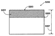
ある特定の実施例では、本発明は、1または複数の光電子部の効率を改善する光導波路を備える太陽電池装置を提供する。前記装置は、第1の表面および第2の表面を含む光透過性基板を有する。光学透明性材料は、第1の屈折率を有する。開口部は、前記光学透明性基板の前記第2の表面の一部に配置される。前記装置は、第1の表面部および第2の表面部を有する第1の半導体材料層を有し、前記第1の表面部は前記光学透明性基板の第1の表面の上を覆っている。光結合材料は、前記材料層の第1の表面部と前記光学透明性基板の第1の表面との間に担持される。前記第1の半導体層は、第2の屈折率を有する。ある特定の実施例では、前記第2の屈折率は、前記第1の屈折率よりも約2ないし3倍大きい。前記装置は、前記第1の半導体材料層の1または複数の部分に形成される光電子部と、前記第1の半導体材料層の1または複数の部分に形成される導波路構造とを有する。 In certain embodiments, the present invention provides a solar cell device comprising an optical waveguide that improves the efficiency of one or more optoelectronic components. The apparatus has a light transmissive substrate including a first surface and a second surface. The optically transparent material has a first refractive index. The opening is disposed on a part of the second surface of the optically transparent substrate. The apparatus includes a first semiconductor material layer having a first surface portion and a second surface portion, the first surface portion covering the first surface of the optically transparent substrate. . The optical coupling material is supported between the first surface portion of the material layer and the first surface of the optically transparent substrate. The first semiconductor layer has a second refractive index. In certain embodiments, the second refractive index is about 2 to 3 times greater than the first refractive index. The device includes an optoelectronic portion formed in one or more portions of the first semiconductor material layer and a waveguide structure formed in one or more portions of the first semiconductor material layer.
ある特定の実施例では、本発明は、太陽電池などの光電子材料の製造方法を提供する。前記製造方法は、単結晶シリコン基板、単結晶ゲルマニウム基板、シリコン−ゲルマニウム基板およびその他などのドナー基板を形成する工程を有する。好ましい実施例では、前記ドナー基板は、劈開部、表面部および前記劈開部と前記表面部との間で定められる第1のシリコン材料層を有する。前記製造方法は、劈開部周辺内部でドナー基板の一部を分離するために、第1のシリコン材料層を処理基板の処理基板表面部に転写する工程を有する。前記製造方法は、第1のシリコン材料層の上を覆う劈開表面部の形成を促すために、前記表面部を前記処理基板の前記処理基板表面部に結合(接合や接着など)する。前記製造方法は、電子サイクロトロン共鳴(ECR)プラズマ蒸着装置あるいは、その他のプラズマを基礎とする適切な装置のように反応室にシラン種(トリシラン種のようなシラン種)を含むガスを供給する工程を有する。好ましい実施例では、前記方法は、前記反応室の内部で前記シラン種を用いる。一例として、前記製造方法は、蒸着を促すために、グロー放電、熱化学蒸着、光強化化学蒸着、一般的にPECVDと呼ばれるプラズマ強化化学蒸着、一般的にLE−PECVDと呼ばれる低エネルギープラズマ強化化学蒸着などを含む1または複数のガス反応技術を用いて、シラン種を含むガスを反応する。本明細書で用いられるように、「PECVD」という用語は、ありふれた意味で解釈されるべきであり、限定されずに誘電結合プラズマ蒸着、容量結合プラズマ蒸着などを含む。前記方法は、シラン種を用いて第1のシリコン材料層の上を覆う第2の材料層を形成する工程を含む。本実施例によれば、本製造方法は、第2のシリコン材料層を結晶化するために、熱処理プロセスで第2の材料層を処理する工程を含む。本実施例によれば、シラン、ジシラン、および、ジクロロシランおよびトリクロロシランのような塩化シランなどのようなトリシラン種以外のシラン種が用いられてもよい。ある特定の実施例では、特定のシラン種の選択は、望ましいあるいは許容される温度、圧力、蒸着中のシラン種の希釈、これらの条件で達成可能な蒸着速度、生成蒸着膜の質に依存する。ある特定の実施例に従えば、ジシランおよびトリシランのようなポリシランは、光電子プロセスに適したガラスに適合するより低温条件下で費用効果の高い蒸着速度を与える。 In one particular embodiment, the present invention provides a method of manufacturing an optoelectronic material such as a solar cell. The manufacturing method includes forming a donor substrate such as a single crystal silicon substrate, a single crystal germanium substrate, a silicon-germanium substrate, and others. In a preferred embodiment, the donor substrate has a cleaved portion, a surface portion, and a first silicon material layer defined between the cleaved portion and the surface portion. The manufacturing method includes a step of transferring the first silicon material layer to the processing substrate surface portion of the processing substrate in order to separate a part of the donor substrate inside the periphery of the cleavage portion. In the manufacturing method, the surface portion is bonded (bonded or adhered) to the processing substrate surface portion of the processing substrate in order to promote formation of a cleaved surface portion covering the first silicon material layer. The manufacturing method includes a step of supplying a gas containing a silane species (a silane species such as a trisilane species) to a reaction chamber as in an electron cyclotron resonance (ECR) plasma deposition apparatus or other suitable plasma-based apparatus. Have In a preferred embodiment, the method uses the silane species inside the reaction chamber. As an example, the manufacturing method includes glow discharge, thermal chemical vapor deposition, photo-enhanced chemical vapor deposition, plasma enhanced chemical vapor deposition commonly referred to as PECVD, and low energy plasma enhanced chemistry commonly referred to as LE-PECVD to facilitate deposition. The gas containing the silane species is reacted using one or more gas reaction techniques including vapor deposition. As used herein, the term “PECVD” should be construed in a common sense and includes, but is not limited to, dielectric coupled plasma deposition, capacitively coupled plasma deposition, and the like. The method includes forming a second material layer overlying the first silicon material layer using a silane species. According to this embodiment, the manufacturing method includes a step of treating the second material layer with a heat treatment process in order to crystallize the second silicon material layer. According to this example, silane species other than trisilane species such as silane, disilane, and chlorosilanes such as dichlorosilane and trichlorosilane may be used. In certain embodiments, the selection of a particular silane species depends on the desired or acceptable temperature, pressure, dilution of the silane species during deposition, the deposition rate achievable under these conditions, and the quality of the resulting deposited film. . According to certain embodiments, polysilanes such as disilane and trisilane provide cost effective deposition rates under lower temperature conditions that are compatible with glasses suitable for optoelectronic processes.
ある特定の実施例では、前記製造方法は、適切な希釈率でH2(水素)ガスを混合したモノシラン(SiH4)ガスを用いる。さらにその他の特定の実施例では、前記製造方法は、適切な希釈率でH2およびヘリウムガスを混合したモノシラン(SiH4)ガスを用いる。もちろん、他に変形し、改良し、あるいは代替することも可能である。 In a specific embodiment, the manufacturing method uses monosilane (SiH 4 ) gas mixed with H 2 (hydrogen) gas at an appropriate dilution rate. In still another specific embodiment, the manufacturing method uses monosilane (SiH 4 ) gas mixed with H 2 and helium gas at an appropriate dilution rate. Of course, other variations, improvements, or alternatives are possible.
もう一つの特定の実施例では、本発明は、光電子材料の基板を製造するその他の方法を提供する。前記製造方法は、ドナー基板を形成する工程を有しており、前記ドナー基板は、劈開部、表面部および前記劈開部と前記表面部との間で定められる第1のシリコン材料層(単結晶シリコン、単結晶ゲルマニウム、シリコン−ゲルマニウムなど)を有する。前記製造方法は、第1のシリコン材料層をガラス、石英、ガラスセラミック、光学透明性材料などの処理基板の処理基板表面部に転写する工程を有する。前記製造方法は、前記表面部を前記処理基板の前記処理基板表面部に結合するために、第1のシリコン材料層の上を覆う劈開部の形成を促して、前記劈開部周辺内部で前記ドナー基板の一部を除去する。前記製造方法は、反応室でシラン種を用いて放電するために、前記反応室にシラン種を含むガスを供給する。一例として、前記製造方法は、グロー放電、プラズマ強化化学蒸着、光強化化学蒸着、あるいは熱化学蒸着(CVD、LPCVD、APCVDなど)などを含む1または複数のガス反応技術を用いて蒸着を促すために、シラン種を含むガスを反応させる。好ましい実施例では、本製造方法は、グロー放電CVD、プラズマCVD、光強化CVDまたは熱CVDなどを用い、シラン種を含有し、第1のシリコン材料層の上を覆う材料を結晶化するための材料の固相エピタキシャル再成長速度と同じ、あるいはこれより速い、あるいはこれより遅い蒸着速度で第1のシリコン材料層を厚くするために、前記劈開部の上を覆う材料を蒸着する工程を有する。 In another specific embodiment, the present invention provides another method of manufacturing a substrate of optoelectronic material. The manufacturing method includes a step of forming a donor substrate. The donor substrate includes a cleavage portion, a surface portion, and a first silicon material layer (single crystal) defined between the cleavage portion and the surface portion. Silicon, single crystal germanium, silicon-germanium, and the like). The manufacturing method includes a step of transferring the first silicon material layer to a processing substrate surface portion of a processing substrate such as glass, quartz, glass ceramic, or an optically transparent material. In the manufacturing method, in order to bond the surface portion to the processing substrate surface portion of the processing substrate, formation of a cleavage portion that covers the first silicon material layer is promoted, and the donor is formed around the cleavage portion. Part of the substrate is removed. In the manufacturing method, in order to discharge using a silane species in the reaction chamber, a gas containing the silane species is supplied to the reaction chamber. As an example, the manufacturing method facilitates deposition using one or more gas reaction techniques including glow discharge, plasma enhanced chemical vapor deposition, light enhanced chemical vapor deposition, or thermal chemical vapor deposition (CVD, LPCVD, APCVD, etc.). And reacting a gas containing silane species. In a preferred embodiment, the manufacturing method uses glow discharge CVD, plasma CVD, photo-enhanced CVD, thermal CVD, or the like to crystallize a material containing a silane species and covering the first silicon material layer. In order to increase the thickness of the first silicon material layer at a deposition rate equal to, faster than, or slower than the solid phase epitaxial regrowth rate of the material, the method includes depositing a material covering the cleaved portion.
もう一つの特定の実施例では、本発明は、光電子材料用基板の製造方法を提供する。前記製造方法は、ドナー基板を形成する工程を有し、前記ドナー基板は劈開部、表面部、および前記劈開部と前記表面部との間で定められる第1のシリコンまたはゲルマニウム材料層を含んでいる。前記製造方法は、劈開部周辺内部のドナー基板の一部を除去するため、および前記表面部を、第1のシリコンまたはゲルマニウム材料層の上を覆う劈開表面部の形成を促して処理基板の処理基板表面部に結合するために、前記第1のシリコンまたはゲルマニウム材料層を処理基板の処理基板表面部に転写する工程も有する。好ましい実施例では、本製造方法は、シランおよび/またはゲルマン種を含有するガスを反応室に供給する工程を含む。本製造方法は、第1のシリコンまたはゲルマニウム材料層を厚くするために、少なくともグロー放電、プラズマ、光強化または熱CVD、シランおよび/またはゲルマン種から選ばれるプロセスを用い、第1のシリコンまたはゲルマニウム材料層の上を覆う材料を結晶化するような材料の固相エピタキシャル再成長速度と等しい、またはこれより大きい、またはこれより小さい蒸着速度で、前記劈開表面の上を覆う第1の材料を蒸着すると好ましい。処理基板の両表面が反応ガスに曝されているバッチ式炉型システムのようなある特定のCVDシステムでは、本製造方法は、少なくとも第1の材料を蒸着する時間の一部で、処理基板の裏面部の上を覆う多結晶またはアモルファス材料を形成するために、前記処理基板の裏面部の上を覆う第2の材料を蒸着してもよい。本実施例によれば、前記第2の材料は、単結晶あるいは、好ましくはアモルファスまたは多結晶であればよい。 In another particular embodiment, the present invention provides a method for manufacturing a substrate for optoelectronic materials. The manufacturing method includes a step of forming a donor substrate, the donor substrate including a cleaved portion, a surface portion, and a first silicon or germanium material layer defined between the cleaved portion and the surface portion. Yes. In the manufacturing method, in order to remove a part of the donor substrate inside the periphery of the cleaved portion and to promote the formation of a cleaved surface portion that covers the surface portion on the first silicon or germanium material layer, the processing substrate is processed. There is also a step of transferring the first silicon or germanium material layer to the processing substrate surface portion of the processing substrate for bonding to the substrate surface portion. In a preferred embodiment, the production method includes the step of supplying a gas containing silane and / or germane species to the reaction chamber. The manufacturing method uses at least a process selected from glow discharge, plasma, photo-enhanced or thermal CVD, silane and / or germane species to thicken the first silicon or germanium material layer, and the first silicon or germanium Depositing a first material overlying the cleaved surface at a deposition rate equal to, greater than, or less than a solid phase epitaxial regrowth rate of the material that crystallizes the material overlying the material layer It is preferable. In certain CVD systems, such as batch furnace systems where both surfaces of the processing substrate are exposed to the reaction gas, the manufacturing method can be performed at least part of the time to deposit the first material on the processing substrate. In order to form a polycrystalline or amorphous material covering the back surface, a second material covering the back surface of the processing substrate may be deposited. According to this embodiment, the second material may be a single crystal, or preferably amorphous or polycrystalline.
さらにもう一つの実施例では、本発明は、光電子装置を提供する。前記装置は、処理基板表面部からなる処理基板を有する。ある特定の実施例では、前記装置は、前記処理基板表面部の上を覆う界面材を有する。層転写フィルムは、前記界面材の上を覆う。ある特定の実施例では、前記装置は、1または複数の欠陥を有する単結晶シリコン、単結晶ゲルマニウム材料または単結晶シリコン−ゲルマニウム合金材料の蒸着層を有する。 In yet another embodiment, the present invention provides an optoelectronic device. The apparatus has a processing substrate composed of a processing substrate surface portion. In a specific embodiment, the apparatus includes an interface material covering the surface portion of the processing substrate. The layer transfer film covers the interface material. In one particular embodiment, the device comprises a deposited layer of single crystal silicon, single crystal germanium material or single crystal silicon-germanium alloy material having one or more defects.
更には、本発明は、光電子装置を提供する。前記装置は、処理基板表面部を構成する処理基板を有する。前記装置は、処理基板の処理基板表面部に転写される第1のシリコンまたはゲルマニウム材料層を有する。前記装置は、第1のシリコンまたはゲルマニウム材料層から調成される劈開表面部も有する。少なくともグロー放電、プラズマ、光強化または熱CVD、およびシランおよび/またはゲルマン種から選ばれるプロセスを用いて調成される蒸着された第1の単結晶シリコンまたはゲルマニウム材料は、前記第1のシリコンまたはゲルマニウム材料層を厚くするために、前記劈開表面の上を覆っている。前記装置は、前記処理基板の裏面部の上を覆うポリまたはアモルファス材料を形成するために、処理基板の裏面部の上を覆って蒸着された第2の材料を有する。 Furthermore, the present invention provides an optoelectronic device. The apparatus has a processing substrate constituting a processing substrate surface portion. The apparatus has a first silicon or germanium material layer that is transferred to the processing substrate surface portion of the processing substrate. The apparatus also has a cleaved surface that is prepared from a first silicon or germanium material layer. The deposited first single crystal silicon or germanium material prepared using at least a process selected from glow discharge, plasma, photo-enhanced or thermal CVD, and silane and / or germane species is said first silicon or In order to thicken the germanium material layer, the cleaved surface is covered. The apparatus has a second material deposited over the back surface of the processing substrate to form a poly or amorphous material over the back surface of the processing substrate.
特に言及されるように、ある実施例では、本製造方法は、グロー放電、プラズマ、光強化または熱CVDなどを用い、シラン種を含み、第1のシリコン材料層の上を覆う材料を結晶化するための材料の固相エピタキシャル再成長速度と同じまたはこれより大きいまたはこれより小さい蒸着速度で、第1のシリコン材料層を厚くするために劈開部の上を覆う材料を蒸着する工程を有する。好ましい実施例では、材料の蒸着速度は、蒸着が生じている間に、原位置(in−situ)で材料を結晶化するような材料の固相エピタキシャル再成長速度と同じか、これよりも小さい。他の実施例では、前記蒸着速度は、結晶性材料を効率的かつ高品質に形成するために、固相エピタキシャル再成長速度よりも僅かに大きい。他の実施例では、蒸着速度がエピタキシャル再成長速度よりも大きいかあるいは遙かに大きい場合、蒸着は、一時的に停止されたり、結晶材料が再成長するために減速されたりする。最終的な層に応じて、本製造方法は、材料を第1の層に蒸着して、前記第1の層の材料を結晶内部で再成長させ、追加の材料を第2の層に蒸着して、前記第2の層を結晶内部で再成長させ、追加の材料を第N(Nは2より大きい整数)の層に蒸着して、第Nの層にある材料を結晶内中で再成長させる。上述したように、蒸着およびエピタキシャル再成長のステップは、ある特定の実施例に係る所望の最終的な層と膜品質が得られるまで繰り返される。もちろん、他に変形し、改良し、あるいは代替することも可能である。 As specifically noted, in some embodiments, the fabrication method uses glow discharge, plasma, photo-enhanced or thermal CVD, etc. to crystallize the material that includes the silane species and overlies the first silicon material layer. Depositing a material overlying the cleaved portion to thicken the first silicon material layer at a deposition rate equal to, greater than or less than the solid phase epitaxial regrowth rate of the material. In a preferred embodiment, the deposition rate of the material is less than or equal to the solid phase epitaxial regrowth rate of the material that crystallizes the material in-situ while deposition occurs. . In another embodiment, the deposition rate is slightly greater than the solid phase epitaxial regrowth rate in order to form the crystalline material efficiently and with high quality. In other embodiments, if the deposition rate is greater than or much greater than the epitaxial regrowth rate, the deposition is temporarily stopped or slowed down due to the crystal material regrowth. Depending on the final layer, the manufacturing method deposits material on the first layer, regrowth of the first layer material inside the crystal, and deposits additional material on the second layer. The second layer is regrown inside the crystal, additional material is deposited on the Nth layer (N is an integer greater than 2), and the material in the Nth layer is regrown in the crystal. Let me. As described above, the deposition and epitaxial regrowth steps are repeated until the desired final layer and film quality according to a particular embodiment is obtained. Of course, other variations, improvements, or alternatives are possible.
特定の実施例では、本発明は、1または複数のソーラーモジュールに用いる太陽電池の製造方法を提供する。本製造方法は、表面部と底部と所定の層を有する支持部材(好ましくは、以下でより詳述される転写用ドナー材料と同等の熱膨張係数(CTE)を有する)を調成する工程を有する。本製造方法は、前記支持部材の表面部の上を覆う脱着可能な材料(粗領域、二酸化ケイ素粗領域など)を形成する工程を有する。好ましい実施例では、前記支持部材は、シリコンエピタキシャル成長などの高温プロセスを可能にするために、再使用可能な媒体として用いられるシリコン基板のような適切な材料から作られてもよい。これらは同一材料であるので、前記支持部材、前記転写シリコン膜およびエピタキシャル成長層の間のCTEは、プロセスに適合できると保証される。後述する説明では、シリコン支持部材は、前記シリコン層転写および前記シリコンエピタキシャル成長に一致する例として用いられているが、前記支持部材は、プロセスの温度範囲、化学処理に抵抗できる異なる材料または材料と層の組み合わせから作製され、汚染が低く、転写フィルムおよび蒸着フィルムに一致する適切なCTEを有し、一回のみの使用が、製造装置の目標コストを裏付けできる程の低コストでない限り、再使用が経済的観点から許容されることを理解すべきである。本製造方法は、前記脱着可能な材料の上を覆うドナー基板から第1のシリコン材料層を転写する工程も有する。本製造方法は、全材料層を形成するために、第1のシリコン材料層の上を覆う第2の半導体材料層を形成する工程を有する。そして、本製造方法は、前記脱着可能な材料から全材料層を除去し、前記全材料層の1または複数の部分に1または複数の光電子装置を形成する。 In certain embodiments, the present invention provides a method for manufacturing a solar cell for use in one or more solar modules. The manufacturing method includes a step of preparing a support member (preferably having a coefficient of thermal expansion (CTE) equivalent to a donor material for transfer described in more detail below) having a surface portion, a bottom portion, and a predetermined layer. Have. The manufacturing method includes a step of forming a detachable material (such as a rough region or a silicon dioxide rough region) covering the surface portion of the support member. In a preferred embodiment, the support member may be made from a suitable material such as a silicon substrate that is used as a reusable medium to allow high temperature processes such as silicon epitaxial growth. Since they are the same material, the CTE between the support member, the transfer silicon film and the epitaxial growth layer is guaranteed to be compatible with the process. In the description below, a silicon support member is used as an example consistent with the silicon layer transfer and the silicon epitaxial growth, but the support member may be a different material or material and layer that can resist process temperature ranges, chemical processing. Can be reused unless the contamination is low, has a suitable CTE that matches the transfer film and the deposited film, and the one-time use is not low enough to support the target cost of the manufacturing equipment It should be understood that this is acceptable from an economic point of view. The manufacturing method also includes a step of transferring a first silicon material layer from a donor substrate covering the detachable material. The manufacturing method includes a step of forming a second semiconductor material layer covering the first silicon material layer in order to form the entire material layer. In this manufacturing method, the entire material layer is removed from the removable material, and one or more optoelectronic devices are formed in one or more portions of the entire material layer.
もう一つの特定の実施例では、本発明は、1または複数のソーラーモジュールに用いる太陽電池の製造方法を提供する。本製造方法は、シリコン支持部材を形成する工程を有する。前記シリコン支持部材は、表面部、底部および前記表面部と前記底部との間に所定の層を有する。本製造方法は、前記シリコン部材の表面部の上を覆う脱着可能な材料を形成する工程を有する。本製造方法は、前記脱着可能な材料の上を覆う第1のシリコン材料層を形成するために、前記脱着可能な材料の上を覆う第1のドナー基板から第1のシリコン材料層を転写し、一方、前記脱着可能な材料は、第1のシリコン材料層を転写する工程を容易にする。好ましい実施例では、前記脱着可能な材料は、前記シリコン部材の上を覆い、前記第1のシリコン材料層を前記脱着可能な材料に接続するのを容易にする表面粗さを有する。本製造方法は、前記脱着可能な材料の上を覆って全材料層を形成するために、前記第1のシリコン材料層の上を覆う第2の半導体材料層を形成する工程も有する。そして、本製造方法は、前記全材料層の1または複数の部分に1または複数の光電子セルを形成し、前記材料層から前記脱着可能な材料を除去する。 In another specific embodiment, the present invention provides a method for manufacturing a solar cell for use in one or more solar modules. The manufacturing method includes a step of forming a silicon support member. The silicon support member has a surface portion, a bottom portion, and a predetermined layer between the surface portion and the bottom portion. The manufacturing method includes a step of forming a detachable material that covers the surface portion of the silicon member. The manufacturing method transfers a first silicon material layer from a first donor substrate covering the detachable material in order to form a first silicon material layer covering the detachable material. On the other hand, the removable material facilitates the process of transferring the first silicon material layer. In a preferred embodiment, the removable material has a surface roughness that covers over the silicon member and facilitates connecting the first silicon material layer to the removable material. The manufacturing method also includes a step of forming a second semiconductor material layer covering the first silicon material layer in order to form an entire material layer over the detachable material. In this manufacturing method, one or a plurality of photoelectron cells are formed in one or a plurality of portions of the entire material layer, and the detachable material is removed from the material layer.
もう一つの特定の実施例では、本発明は、1または複数のソーラーモジュールに用いる太陽電池の製造方法を提供する。本製造方法は、支持部材を形成する工程を有する。前記支持部材は、表面部、底部、および前記表面部と底部との間に所定の層を有してもよい。前記支持部材は、ある特定の実施例でのキャリア素子であってもよい。本製造方法は、前記支持部材の上を覆う第1のシリコン材料層を形成するために、前記支持部材の上を覆う第1のドナー基板から第1のシリコン材料層を転写する。そして、本製造方法は、前記支持部材の上を覆う全材料層を形成するために、第1のシリコン材料層の上を覆う第2の半導体材料層を形成する。そして、本製造方法は、全材料層の1または複数の部分に1または複数の光電子材料を形成する。 In another specific embodiment, the present invention provides a method for manufacturing a solar cell for use in one or more solar modules. This manufacturing method has the process of forming a supporting member. The support member may have a surface portion, a bottom portion, and a predetermined layer between the surface portion and the bottom portion. The support member may be a carrier element in a specific embodiment. In this manufacturing method, in order to form the first silicon material layer that covers the support member, the first silicon material layer is transferred from the first donor substrate that covers the support member. And in this manufacturing method, in order to form the whole material layer which covers the said support member, the 2nd semiconductor material layer which covers the 1st silicon material layer is formed. And this manufacturing method forms one or several optoelectronic materials in the one or several part of all the material layers.
さらにもう一つの実施例では、本発明は、太陽電池や集積回路を含む他の同様な基板を製造する装置を提供する。前記装置は、表面部、底部および前記表面部と前記底部の間に所定の層を有する支持部材を有する。1または複数の開口(単一形状、配列形状および円形状など)は、前記支持部材の表面部に、空間的な形状で備えられる。流体源は1または複数の開口に結合される。特定の実施例では、前記流体源は、前記支持部材の表面部で、1または複数の開口を貫いて流体を供給するのに適している。脱着可能な材料は、前記支持部材の表面部の上を覆っている。前記装置は、前記脱着可能な材料の上を覆う第1の転写材料層を形成するために、前記脱着可能な材料の上を覆う第1の半導体材料層を有し、第1の半導体材料層は、前記支持部材の上を覆う。本実施例によれば、他に変形し、改良し、あるいは代替することも可能である。 In yet another embodiment, the present invention provides an apparatus for manufacturing other similar substrates including solar cells and integrated circuits. The apparatus includes a surface portion, a bottom portion, and a support member having a predetermined layer between the surface portion and the bottom portion. One or a plurality of openings (single shape, array shape, circular shape, etc.) are provided in a spatial shape on the surface portion of the support member. A fluid source is coupled to the one or more openings. In certain embodiments, the fluid source is suitable for supplying fluid through one or more openings at the surface of the support member. The removable material covers the surface portion of the support member. The apparatus has a first semiconductor material layer overlying the removable material to form a first transfer material layer overlying the removable material. Covers the support member. According to the present embodiment, other modifications, improvements, or alternatives are possible.
本発明を用いれば、数多くの恩恵が、既存の技術を超えて得られる。特に本発明は、ある特定の実施例に従って、選択的にガラス基板上面の薄い光電子膜を劈開するために、制御されたエネルギーと選択された条件を用いる。ある特定の実施例では、本発明の製造方法および装置は、ガラス上に極めて高品質の光電子材料を備え、前記光電子材料は、パッケージング材の一部として用いられてもよい。好ましい実施例では、本発明の製造方法および構造で実現されるのは、太陽電池を使用して高効率の電力を供給するための単結晶シリコンである。 With the present invention, numerous benefits are gained over existing technologies. In particular, the present invention uses controlled energy and selected conditions to selectively cleave a thin optoelectronic film on the top surface of a glass substrate in accordance with certain embodiments. In certain embodiments, the manufacturing method and apparatus of the present invention comprises a very high quality optoelectronic material on glass, which may be used as part of a packaging material. In a preferred embodiment, what is realized with the manufacturing method and structure of the present invention is single crystal silicon for supplying highly efficient power using solar cells.
さらに、本発明の製造方法で実現されるのは、高成長速度厚膜プロセスであり、前記高成長速度厚膜プロセスは、ある特定の実施例に従って、望ましい温度特性を有する。つまり、ある特定の実施例に従って、本製造方法で実現されるのは、ガラス処理基板材が損傷を受けない結晶材料または結晶化される材料の蒸着である。他の実施例において、前記製造方法で実現されるのは、基板部材の正面側および裏面側での光電子材料の形成である。本実施例によれば、1または複数のこれらの恩恵が得られる。これらおよび他の恩恵は、本明細書、特に以下でより詳述に開示される。 Furthermore, what is realized in the manufacturing method of the present invention is a high growth rate thick film process, which has desirable temperature characteristics according to a specific embodiment. That is, according to a particular embodiment, what is realized in the present manufacturing method is the deposition of a crystalline material or a crystallized material that does not damage the glass-treated substrate material. In another embodiment, the manufacturing method realizes the formation of optoelectronic materials on the front side and the back side of the substrate member. According to the present embodiment, one or more of these benefits can be obtained. These and other benefits are disclosed in more detail herein, particularly below.
さらに、本発明に係る実施例は、過度のエネルギー放出および/または熱エネルギーからこのようなフィルムへ損傷を与える可能性なく、材料の薄い光電子フィルムを選択的に劈開および処理するために、制御されたエネルギーと選択された条件を用いる。この劈開プロセスは、前記フィルムまたは前記基板の残存部分への損傷の可能性を防ぐと同時に、基板から薄い光電子フィルムを選択的に除去する。さらに、本発明の製造方法および構造で実現されるのは、一連の半導体プロセスを通じて基板に備えられる劈開層を用いたさらに効率的なプロセスであり、前記効率的なプロセスは、ある特定の実施例に従って、より高温で実行される。ある特定の実施例では、処理基板に備えられる劈開フィルムは、前記劈開フィルムと前記処理基板との間に備えられる界面部周辺内部に欠陥が形成されることなく、前記劈開フィルムを前記処理基板に強固に固定するために、速熱処理プロセスに曝される。好ましい実施例では、本発明の製造方法および構造で実現されるのは、光電子セルを用いて効率的な電力を供給するための単結晶シリコンである。好ましい実施例では、本発明の製造方法および構造は、2つの材料間での装着および2つの材料の互いからの除去を容易にする脱着可能な材料を用いる。本実施例によれば、1または複数のこれらの恩恵が受けられるであろう。これらおよびその他の恩恵は、本明細書、特に以下でより詳細に開示される。 In addition, embodiments according to the present invention are controlled to selectively cleave and process thin optoelectronic films of material without the possibility of damaging such films from excessive energy release and / or thermal energy. Energy and selected conditions. This cleaving process selectively removes a thin optoelectronic film from the substrate while preventing possible damage to the film or the remaining portion of the substrate. Furthermore, what is realized with the manufacturing method and structure of the present invention is a more efficient process using a cleaving layer provided on a substrate through a series of semiconductor processes, which is a specific embodiment. And run at higher temperatures. In a specific embodiment, the cleaved film provided on the processing substrate has the cleaved film formed on the processing substrate without any defects formed in the periphery of the interface provided between the cleaving film and the processing substrate. To be firmly fixed, it is exposed to a rapid heat treatment process. In a preferred embodiment, what is realized with the manufacturing method and structure of the present invention is single crystal silicon for providing efficient power using an optoelectronic cell. In a preferred embodiment, the manufacturing method and structure of the present invention uses a removable material that facilitates attachment between two materials and removal of the two materials from each other. According to this embodiment, one or more of these benefits will be received. These and other benefits are disclosed in more detail herein, particularly below.
本発明によって得られるのは、公知プロセス技術に関連するこれらの恩恵と他の恩恵である。しかしながら、本発明の特質と利点の更なる理解は、本明細書の後半部分と添付の図面を参照して実現される。 These and other benefits associated with known process technology are obtained by the present invention. However, a further understanding of the nature and advantages of the present invention may be realized by reference to the latter portions of the specification and attached drawings.
本発明の実施例によれば、光電子材料の製造に対する技術が提供される。より詳しくは、本発明に係る1つの実施例は、光電子アプリケーションに対する層転写技術を用いて太陽電池の構造を形成するための方法と構造とを含む技術を提供する。本発明に係る他の実施例は、光電子装置の製造のための望ましい蒸着速度と熱量を有するシラン基種を用いた光電子厚膜プロセスを提供する。本発明に係るある特定の実施例は、ジシランまたはトリシラン基種を利用しているが、ある特定の実施例によれば、その他のシラン種を用いることもできる。前記実施形態によれば、常圧CVD(APCVD)、原子層CVD(ALCVD)(原子層エピタキシーおよび原子層蒸着(ALD)など)、エアロゾルアシストCVD(AACVD)、直接液体注入CVD(DLICVD)、熱線CVD(HWCVD)(触媒CVD(Cat−CVD)または熱フィラメントCVD(HFCVD))、低圧CVD(LPCVD)、マイクロ波プラズマアシストCVD(MPCVD)、プラズマ強化CVD(PECVD)、急熱CVD(RTCVD)、遠隔プラズマ強化CVD(RPECVD)、超真空CVD(UHVCVD)などを含む種々の技術を用いて、蒸着が起こってもよい。しかし、本発明は、より広い範囲に適用できることが認識されるであろう。つまり、本発明は、集積半導体装置の三次元パッケージング、フォトニック装置、ピエゾエレクトリック・デバイス、フラットパネルディスプレイ、微小電気機械システム(MEMS)、ナノテクノロジー構造、センサー、アクチュエーター、集積回路、生物学的および生物医学的装置などのような他の種類のアプリケーションに適用できる。 According to embodiments of the present invention, techniques for the production of optoelectronic materials are provided. More particularly, one embodiment of the present invention provides a technique that includes a method and structure for forming a solar cell structure using layer transfer techniques for optoelectronic applications. Another embodiment according to the present invention provides an optoelectronic thick film process using a silane based species having the desired deposition rate and heat value for the manufacture of optoelectronic devices. Although certain embodiments of the present invention utilize disilane or trisilane base species, other silane species may be used according to certain embodiments. According to the embodiment, atmospheric pressure CVD (APCVD), atomic layer CVD (ALCVD) (such as atomic layer epitaxy and atomic layer deposition (ALD)), aerosol assisted CVD (AACVD), direct liquid injection CVD (DLICVD), hot wire CVD (HWCVD) (catalytic CVD (Cat-CVD) or hot filament CVD (HFCVD)), low pressure CVD (LPCVD), microwave plasma assisted CVD (MPCVD), plasma enhanced CVD (PECVD), rapid thermal CVD (RTCVD), Deposition may occur using various techniques including remote plasma enhanced CVD (RPECVD), ultra-vacuum CVD (UHVCVD), and the like. However, it will be appreciated that the present invention is applicable to a wider range. In other words, the present invention relates to three-dimensional packaging of integrated semiconductor devices, photonic devices, piezoelectric devices, flat panel displays, microelectromechanical systems (MEMS), nanotechnology structures, sensors, actuators, integrated circuits, biological And other types of applications such as biomedical devices.
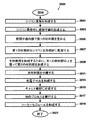
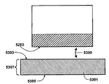
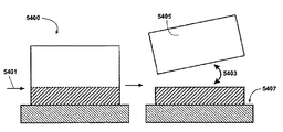
半導体基板上の光電子層を製造する方法は、以下で概説される。
(1)半導体基板を形成する。半導体基板は、表面部、劈開部および前記表面部と前記劈開部の間にあって、除去される第1の材料層を有する。
(2)光学透明性基板に半導体基板を配置する。
(3)光学透明性基板の第1の表面部に半導体基板の表面部を結合する。
(4)劈開部の一部で、制御された劈開動作を開始する。
(5)半導体基板から第1の材料層を除去するため、半導体基板を劈開する。一方、劈開表面部の形成を促すために、前記表面部は、前記第1の表面部に結合されたままとなっている。
(6)半導体材料の生成層を形成するために、(例えば、シラン種を用いて)劈開表面部の上を覆って、第2の半導体材料層を形成する。半導体材料の生成層は、1または複数の光電子部を有する。
(7)第2の半導体材料層の上を覆って、カバーガラス材料を取り付ける。
(8)必要に応じて、その他のステップを実行する。
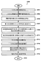
A method for producing an optoelectronic layer on a semiconductor substrate is outlined below.
(1) A semiconductor substrate is formed. The semiconductor substrate has a surface portion, be between the cleave region and the cleave region and the surface region, has a first material layer to be removed.
(2) A semiconductor substrate is placed on an optically transparent substrate.
(3) The surface portion of the semiconductor substrate is bonded to the first surface portion of the optically transparent substrate.
(4) A controlled cleavage operation is started at a part of the cleavage unit.
(5) The semiconductor substrate is cleaved to remove the first material layer from the semiconductor substrate. On the other hand, in order to promote the formation of the cleaved surface portion, the surface portion remains coupled to the first surface portion.
(6) To form a semiconductor material generation layer, a second semiconductor material layer is formed over the cleaved surface (eg, using a silane species). The generation layer of the semiconductor material has one or more optoelectronic parts.
(7) A cover glass material is attached to cover the second semiconductor material layer.
(8) Perform other steps as necessary.
上記一連のステップによって、本発明の実施例に係る製造方法が実現される。以下に示すように、本技術は、光電子アプリケーションに層転写技術を用いて太陽電池の構造を形成する方法および構造を含む。好ましい実施例では、第2の材料層を形成するために、前記方法はシラン種の反応ガスを用いており、前記第2の材料層は、第1の材料層を厚くする。あるいは、請求項の範囲から逸脱することなく、ステップが追加されたり、1または複数のステップが除去されたり、あるいは1または複数のステップが異なるシーケンスに設けられたりしてもよい。例えば、1つの実施例では、第2の半導体材料層が形成される前に、シード層が、劈開表面部の上方にグラフォエピタキシーに形成されてもよい。 The manufacturing method according to the embodiment of the present invention is realized by the series of steps described above. As shown below, the present technology includes methods and structures for forming solar cell structures using layer transfer techniques for optoelectronic applications. In a preferred embodiment, the method uses a reactive gas of silane species to form a second material layer, and the second material layer thickens the first material layer. Alternatively, steps may be added, one or more steps may be removed, or one or more steps may be provided in different sequences without departing from the scope of the claims. For example, in one embodiment, a seed layer may be formed graphoepitaxy above the cleaved surface before the second semiconductor material layer is formed.
あるいは、前記構造を形成する他の方法を用いることもできる。つまり、前記シーケンスが、カバーガラスおよびその他の適切な材料のようなカバーシートに最初に形成され、その後、ある特定の実施例に基づくその他の層を形成することもできる。前記層転写は、カバーガラス上で生じ、前記カバーガラスは、太陽電池装置の残余部を形成するのに用いられる。他の技術では、層転写材料を処理基板の上に転写する転写基板を用いることもできる。本発明の方法のさらなる詳細は、本明細書、特に以下で詳述される。 Alternatively, other methods for forming the structure can be used. That is, the sequence can first be formed on a cover sheet, such as a cover glass and other suitable materials, and then other layers based on a particular embodiment can be formed. The layer transfer occurs on the cover glass, which is used to form the remainder of the solar cell device. Other techniques may use a transfer substrate that transfers the layer transfer material onto the processing substrate. Further details of the method of the present invention are detailed herein and in particular below.
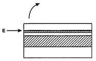
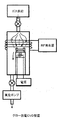
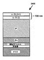
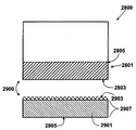
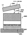
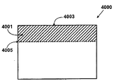
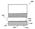
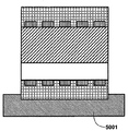
図1で示すように、本製造方法は透明性処理基板を調成し、前記透明性処理基板は、第1の撓み特性、裏面および表面を有する。前記透明処理基板は、ガラス、石英、ガラスセラミック、ポリマーまたはその他の合成物などであってもよい。一例を挙げれば、前記透明基板は、層、裏面および表面を有する。前記透明基板は、太陽電池などを覆うのに用いられるようなガラスである。本実施例によれば、前記ガラスはある程度柔軟であるので、剛性を得るために裏板に固定されるべきである。もちろん、他に変形、修正、あるいは代替することも可能である。 As shown in FIG. 1, the manufacturing method prepares a transparent processed substrate, and the transparent processed substrate has a first deflection characteristic, a back surface, and a front surface. The transparent processing substrate may be glass, quartz, glass ceramic, polymer, or other composite. For example, the transparent substrate has a layer, a back surface, and a front surface. The transparent substrate is glass that is used to cover solar cells and the like. According to this embodiment, the glass is flexible to some extent and should be fixed to the back plate in order to obtain rigidity. Of course, other variations, modifications, or alternatives are possible.
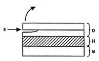
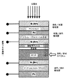
もう一つの実施例では、前記処理基板は均質な材料、組成が徐々に変化する材料、または多層の材料、あるいはこれらのいずれかの組み合わせであってもよい。つまり、前記処理基板は、ほとんど全ての単結晶、多結晶、さらにはアモルファス型基板から作られてもよい。さらに、前記基板は、ヒ化ガリウム、窒化ガリウム(GaN)などのようなIII/V材料から作られてもよい。さらに、前記基板は、シリコンカーバイド、ゲルマニウム、シリコン、ガラス、ガラスセラミック、あるいは、合成石英、プラスチック、およびポリマーであってもよく、柔軟な特性を有する。前記処理基板は、ある特定の実施例に係る層転写プロセスには適さないある程度柔軟な特性を有すると好ましい。前記基板の不適切な性質は、ある特定の実施例によれば、過度の粗さ、破損、部分的な膜剥離などの原因となる。材料の他の全ての組み合わせが、ある特定の実施例によって用いられてもよい。 In another embodiment, the processing substrate may be a homogeneous material, a material with gradually changing composition, a multilayer material, or any combination thereof. That is, the processing substrate may be made of almost all single crystal, polycrystal, or even amorphous type substrates. Further, the substrate may be made from III / V materials such as gallium arsenide, gallium nitride (GaN), and the like. Further, the substrate may be silicon carbide, germanium, silicon, glass, glass ceramic, or synthetic quartz, plastic, and polymer, and has flexible properties. Preferably, the treated substrate has some degree of flexibility that is not suitable for the layer transfer process according to certain embodiments. Inappropriate properties of the substrate may cause excessive roughness, breakage, partial delamination, etc., according to certain embodiments. All other combinations of materials may be used according to a particular embodiment.
好ましい実施例では、本発明は、図2に示すように、処理基板の構造に剛性を加えるために、裏基板を備えている。前記裏基板は、前記処理基板の上に転写されるようなドナー基板からのシリコン支持材料の層に適するように、少なくとも裏基板と処理基板から構成される有効な撓み特性を有する多層構造を調成するに足る厚さと材料とを有すると好ましい。 In a preferred embodiment, the present invention comprises a back substrate to add rigidity to the structure of the processing substrate, as shown in FIG. The back substrate has a multi-layer structure with effective flexural properties comprised of at least the back substrate and the treatment substrate so as to be suitable for a layer of silicon support material from the donor substrate as transferred onto the treatment substrate. It is preferable to have a thickness and material sufficient to achieve.
一例を挙げれば、前記裏基板は、石英処理基板用のシリコンウエーハである。このような裏基板は、725±15ミクロンの厚さを有し、例えば、200ミリメーターのドナー/処理/裏基板構造を用いた単結晶シリコンから作られる。このような基板は、約130ギガパスカルのヤング率を有する。プラスチック、金属、ガラス、ガラスセラミック、石英、複合材料などの他の種類の材料および所定の層は、一体にされた裏基板および処理基板構造に剛性を与えるために用いられてもよい。もちろん、当該技術分野における通常の知識の1つに基づいて、他に変形し、修正し、あるいは代替することが認識されるであろう。 In one example, the back substrate is a silicon wafer for a quartz processing substrate. Such a back substrate has a thickness of 725 ± 15 microns and is made, for example, from single crystal silicon using a 200 millimeter donor / process / back substrate structure. Such a substrate has a Young's modulus of about 130 gigapascal. Other types of materials such as plastic, metal, glass, glass ceramic, quartz, composite materials and certain layers may be used to provide rigidity to the integrated back and processing substrate structures. Of course, it will be appreciated that other variations, modifications, or alternatives will be based on one of ordinary skill in the art.
あるオプションの特定の実施例では、本製造方法は、図3および図4に示すように、裏側および/または透明処理基板の表面で、洗浄および/または活性化工程(プラズマ活性工程など)を実行する。このようなプラズマ活性工程は、基板の表面を洗浄および/または活性化する。前記プラズマ活性工程は、酸素と窒素を含んだプラズマを20〜40℃で使用することで実現される。前記プラズマ活性工程は、カリフォルニア州サンノゼのシリコン・ジェネシス社(Silicon Genesis Corporation)で製造される2周波共用プラズマ活性化装置で実行されるとよい。別の実施例では、いかなる裏材を有さなくてもよい。あるいは、さらに別の実施例では、本発明の製造方法は、静電チャックおよび/またはポーラスチャックなどを介して裏材を用いてもよい。ある特定の実施例に基づいて、本発明の裏材は、処理基板またはドナー基板のいずれか、処理基板またはドナー基板の双方に備えられてもよい。もちろん、他に変形し、改良し、あるいは代替することも可能である。 In one optional specific embodiment, the manufacturing method performs a cleaning and / or activation process (such as a plasma activation process) on the backside and / or the surface of the transparent processing substrate, as shown in FIGS. To do. Such a plasma activation process cleans and / or activates the surface of the substrate. The plasma activation process is realized by using a plasma containing oxygen and nitrogen at 20 to 40 ° C. The plasma activation process may be performed by a dual frequency plasma activation apparatus manufactured by Silicon Genesis Corporation of San Jose, California. In another embodiment, it may not have any backing. Alternatively, in yet another embodiment, the manufacturing method of the present invention may use a backing material via an electrostatic chuck and / or a porous chuck. Based on certain embodiments, the backing of the present invention may be provided on either the processing substrate or the donor substrate, both on the processing substrate or the donor substrate. Of course, other variations, improvements, or alternatives are possible.
図5を参照すると、本製造方法は、透明処理基板の裏側へ裏基板の係合を開始する。前記係合は、しばしば他の構造から物理的に除去される。本製造方法は、多層構造を形成する前記透明処理基板に裏基板を強固に係合するために、前記透明処理基板の裏側に裏基板を一時的に取り付けるとよい。一例を挙げれば、シリコンウエーハの裏基板は、好ましい実施例に係る他のいかなる形態および/または代替によらず、石英板に強固に取り付けられる。さて、自然酸化物によらない実施例もあり得るが、図6に示すように、前記シリコンウエーハは、自然酸化物の非常に薄いコーティングを有し、前記コーティングは、前記石英板の表面と結合する。他の実施例では、共有結合を含む静電プロセスあるいはウェブ結合(web bonding)、あるいはこれらの任意の組み合わせなどを用いて、結合が生じてもよい。さらにもう一つの実施例では、スピンオンガラス、接着剤層または、これらの任意の組み合わせなどを用いて、前記結合が生じてもよい。もちろん、他に変形し、改良し、あるいは代替することも可能である。 Referring to FIG. 5, the manufacturing method starts engagement of the back substrate to the back side of the transparent processing substrate. The engagement is often physically removed from other structures. In this manufacturing method, the back substrate may be temporarily attached to the back side of the transparent processing substrate in order to firmly engage the back substrate with the transparent processing substrate forming a multilayer structure. In one example, the back substrate of the silicon wafer is rigidly attached to the quartz plate without any other form and / or alternative according to the preferred embodiment. There may be embodiments that do not rely on native oxide, but as shown in FIG. 6, the silicon wafer has a very thin coating of native oxide that is bonded to the surface of the quartz plate. To do. In other embodiments, the bonding may occur using an electrostatic process including covalent bonding, web bonding, or any combination thereof. In yet another embodiment, the bonding may occur using spin-on glass, an adhesive layer, or any combination thereof. Of course, other variations, improvements, or alternatives are possible.
本製造方法は、図7に示すように、劈開部、表面、裏面、および前記表面と前記劈開部との間のシリコン支持材料の層を含むドナー基板を形成する工程を含む。一例を挙げれば、前記ドナー基板は、シリコンウエーハ、ゲルマニウムウエーハ、シリコン−ゲルマニウム材料、シリコンカーバイド支持材料、III/V族化合物およびこれらの任意の組み合わせなどであればよい。好ましい実施例では、前記ドナー基板は、感光性材料を用いて作られる。もちろん、他に変形し、改良し、あるいは代替することも可能である。 As shown in FIG. 7, the manufacturing method includes a step of forming a donor substrate including a cleaved portion, a front surface, a back surface, and a layer of a silicon support material between the front surface and the cleaved portion. For example, the donor substrate may be a silicon wafer, a germanium wafer, a silicon-germanium material, a silicon carbide support material, a III / V group compound, and any combination thereof. In a preferred embodiment, the donor substrate is made using a photosensitive material. Of course, other variations, improvements, or alternatives are possible.
前記実施例によれば、劈開部は種々の技術を用いて形成されてもよい。つまり、前記劈開部は、注入粒子、蒸着層、拡散物質、パターン領域およびその他の技術の任意の適切な組み合わせを用いて形成されてもよい。図6を参照すると、本製造方法は、注入プロセスを用いて、所定のエネルギー粒子をドナー基板の上面を通って選択深度まで導入する。前記選択深度は、材料の「薄膜」と呼ばれる材料部の厚さを定める。シリコンウエーハにエネルギー粒子を注入するために、種々の技術が用いられてもよい。これらの技術は、例えば、アプライド・マテリアル社(Applied Material,Inc)などのような会社から製造されるビーム・ライン・イオン注入装置を用いたイオン注入を含む。あるいは、プラズマ浸漬イオン注入(”PIII”)技術、イオンシャワー、および他の非質量的な特別な技術を用いて、注入がなされる。そのような技術の組み合わせが、用いられてもよい。もちろん、アプリケーションに応じた技術が用いられる。 According to the embodiment, the cleaved portion may be formed using various techniques. That is, the cleaved portion may be formed using any appropriate combination of injected particles, vapor deposition layer, diffusing material, pattern region, and other techniques. Referring to FIG. 6, the present manufacturing method introduces predetermined energetic particles through the upper surface of the donor substrate to a selected depth using an implantation process. The selected depth defines the thickness of the material part called the “thin film” of the material. Various techniques may be used to inject energetic particles into the silicon wafer. These techniques include, for example, ion implantation using a beam line ion implanter manufactured from a company such as Applied Material, Inc. Alternatively, implantation is performed using plasma immersion ion implantation ("PIII") techniques, ion showers, and other non-mass special techniques. A combination of such techniques may be used. Of course, a technique according to the application is used.
前記アプリケーションによれば、好ましい実施例に係る通常より小さい質量粒子が、材料部に対する損傷の可能性を低減するように選ばれる。つまり、より小さい質量粒子は、粒子が横断する前記材料部に実質的に損傷を与えることなく、前記基板材料を通って選択深度まで容易に伝播する。例えば、より小さい質量粒子(あるいはエネルギー粒子)は、ほぼ全ての荷電(正または負など)粒子および/または、中性原子または分子、あるいは電子などであってもよい。ある特定の実施例では、前記粒子は、中性粒子および/または、水素のイオンおよびその同位元素のようなイオン、ヘリウムおよびその同位元素、並びにネオンのような希ガスイオン、あるいは本実施例に従ってその他のイオンを含む荷電粒子であってもよい。前記粒子は、水素ガス、水蒸気、メタン、および水素化合物などのガス、並びにその他の軽量の原子質量粒子のような化合物から誘導されてもよい。あるいは、前記粒子は、上記粒子および/またはイオンおよび/または分子種および/または原子種の如何なる組み合わせであってもよい。前記粒子は、一般的に、前記表面を通って前記表面下の選択深度まで貫くための十分な運動エネルギーを有している。 According to said application, smaller than normal mass particles according to a preferred embodiment are chosen so as to reduce the possibility of damage to the material part. That is, smaller mass particles easily propagate through the substrate material to a selected depth without substantially damaging the material section that the particles traverse. For example, the smaller mass particles (or energetic particles) may be almost all charged (such as positive or negative) particles and / or neutral atoms or molecules, or electrons. In certain embodiments, the particles are neutral particles and / or ions such as hydrogen ions and their isotopes, helium and its isotopes, and noble gas ions such as neon, or according to this embodiment. Charged particles containing other ions may be used. The particles may be derived from compounds such as hydrogen gas, water vapor, methane, and hydrogen compounds, and other lightweight atomic mass particles. Alternatively, the particles may be any combination of the particles and / or ions and / or molecular species and / or atomic species. The particles generally have sufficient kinetic energy to penetrate through the surface to a selected depth below the surface.
一例として、シリコンウエーハ内部への注入種として水素を用いる場合、ある特定の一連の条件を用いることで、注入プロセスが実行される。注入量は、約1×10e15原子/cm2から約1×10e18原子/cm2の範囲にあり、好ましくは、前記注入量は約1×10e16原子/cm2以上であるとよい。注入エネルギーは、約1KeVから約1MeVの範囲にあり、通常約50KeVである。注入温度は、約20℃から約600℃の範囲にあり、注入シリコンウエーハから相当量の水素イオンが拡散する可能性、注入損傷およびストレスのアニールを回避するために、400℃以下であるとよい。前記水素イオンは、選択深度に対して約±0.03ミクロンから±0.05ミクロンの精度で、前記シリコンウエーハの内部に選択的に導入されてもよい。もちろん、用いられるイオンの種類とプロセス条件は、アプリケーション次第である。 As an example, when hydrogen is used as the implantation species into the silicon wafer, the implantation process is performed using a specific series of conditions. The implantation amount is in the range of about 1 × 10e 15 atoms / cm 2 to about 1 × 10e 18 atoms / cm 2 , and preferably the implantation amount is about 1 × 10e 16 atoms / cm 2 or more. The implantation energy is in the range of about 1 KeV to about 1 MeV, usually about 50 KeV. The implantation temperature is in the range of about 20 ° C. to about 600 ° C. and may be 400 ° C. or less to avoid the possibility of significant amounts of hydrogen ions diffusing from the implanted silicon wafer, implantation damage and stress annealing. . The hydrogen ions may be selectively introduced into the silicon wafer with an accuracy of about ± 0.03 microns to ± 0.05 microns with respect to a selected depth. Of course, the type of ions used and the process conditions depend on the application.
前記注入粒子は、選択深度にある基板の頂面に平行な平面に沿って、ストレスを加えたり、破損エネルギーを減じたりすると効果的である。前記エネルギーは、ある程度、注入種および注入条件に依存する。これらの粒子は、選択深度にある基板の破損エネルギーレベルを減ずる。これにより、選択深度にある注入面に沿って制御された劈開が実現される。注入は、基板のエネルギー状態が、全ての内部の場所で、基板材料で不可逆的な破損(分離あるいは劈開など)を開始するのに不十分な条件下で生じてもよい。しかしながら、注入が基板内部である程度の欠陥(マイクロ検出など)を概して誘発することに留意すべきである。前記欠陥は、典型的には、熱アニールまたは速熱アニールなどの以降の熱処理によって少なくとも部分的に修復される。注入を受けている生成基板は、図7に概略図で示される。 The implanted particles are effective when applying stress or reducing breakage energy along a plane parallel to the top surface of the substrate at a selected depth. The energy depends to some extent on the implantation species and implantation conditions. These particles reduce the failure energy level of the substrate at the selected depth. This achieves a controlled cleavage along the injection surface at the selected depth. Implantation may occur under conditions where the energy state of the substrate is insufficient to initiate irreversible damage (such as separation or cleavage) with the substrate material at all internal locations. However, it should be noted that implantation generally induces some degree of defects (such as micro detection) within the substrate. The defects are typically at least partially repaired by subsequent heat treatments such as thermal annealing or rapid thermal annealing. The production substrate undergoing implantation is shown schematically in FIG.
本実施例によれば、劈開部および/または劈開層を形成するために、その他の技術を用いてもよい。一例を挙げれば、そのような劈開部は、カリフォルニア州のサンタクララにあるシリコン・ジェネシス社(Silicon Genesis Corporation)のナノ劈開(Nanocleave(商標))プロセス、フランスにあるソイテックSA(Soitec SA)のスマートカット(SmartCut(商標名))プロセスおよび日本の東京にあるキャノン株式会社のエルトラン(Eltran(商標名))プロセスなどと呼ばれるようなその他のプロセスを用いて形成される。もちろん、他に変形し、改良し、あるいは代替することも可能である。 According to this embodiment, other techniques may be used to form the cleaved portion and / or the cleaved layer. In one example, such cleavages are the Silicon Genese Corporation nanocleavage process in Santa Clara, California, the Soytec SA smart in France. It is formed using other processes such as the cut (SmartCut (TM)) process and the Eltran (TM) process of Canon Inc. in Tokyo, Japan. Of course, other variations, improvements, or alternatives are possible.
ある特定の実施例では、裏側に接続された透明処理基板とドナー基板は、図8に示されたように、共にプラズマ活性プロセスに供される。そのようなプラズマ活性プロセスは、基板の表面を洗浄および/または活性化する。前記プラズマ活性プロセスは、20℃から40℃で酸素あるいは窒素を含んだプラズマを用いて実現される。前記プラズマ活性プロセスは、カリフォルニア州サンノゼにあるシリコン・ジェネシス社(Silicon Genesis Corporation)で製造される2周波共用プラズマ活性化装置で実行されるとよい。もちろん、他に変形し、改良し、あるいは代替することも可能であり、それらは、本明細書外で記述されるのと同様にここに記述されている。 In one particular embodiment, the transparent processing substrate and the donor substrate connected to the back side are both subjected to a plasma activation process, as shown in FIG. Such a plasma activation process cleans and / or activates the surface of the substrate. The plasma activation process is realized using a plasma containing oxygen or nitrogen at 20 ° C. to 40 ° C. The plasma activation process may be performed in a dual frequency plasma activation device manufactured by Silicon Genesis Corporation of San Jose, California. Of course, other variations, modifications, or alternatives are possible and are described herein as described elsewhere herein.
その後、これらの基板のそれぞれは、図9で示されるように、互いに結合される。図示されるように、前記処理基板は、ドナーウエーハに結合されている。前記基板は、エレクトロニック・ヴィジョン・グループ(Electronic Vision Group)で製造されたEVG850ボンディング工具あるいは他の同様のプロセスを用いて結合されてもよい。また、カール・サス(Karl Suss)によって製造されるような他の種類の工具が、用いられてもよい。もちろん、他に変形し、改良し、あるいは代替することも可能である。前記透明処理基板と前記ドナー基板の間の結合は、十分に長持ちし高い信頼性を有すると好ましい。 Each of these substrates is then bonded together as shown in FIG. As shown, the processing substrate is coupled to a donor wafer. The substrates may be bonded using an EVG850 bonding tool manufactured by an Electronic Vision Group or other similar process. Other types of tools such as those manufactured by Karl Sus may also be used. Of course, other variations, improvements, or alternatives are possible. The bond between the transparent processing substrate and the donor substrate is preferably long-lasting and highly reliable.
結合後には、結合構造は加熱処理に供される。前記加熱処理は、所定温度および所定時間で結合基板を維持する。温度は、約200℃または250℃から約400℃の範囲にあれば好ましく、シリコンドナー基板および透明処理基板に対して、約1時間程度約350℃であればより好ましい。ある特定の実施例では、前記加熱処理は、ホットプレートから結合基板まで直接的に熱エネルギーを供給するホットプレートおよび/または表面で伝導加熱プロセスを用いて行われてもよい。他の実施例では、熱エネルギーが、放射線、伝導性、対流、またはこれらの技術のあらゆる組み合わせなどを用いて供給されてもよい。ある特定の実施例によれば、他に変形し、改良し、あるいは代替することも可能である。 After bonding, the bonded structure is subjected to heat treatment. The heat treatment maintains the bonded substrate at a predetermined temperature and a predetermined time. The temperature is preferably about 200 ° C. or in the range of 250 ° C. to about 400 ° C., and more preferably about 350 ° C. for about 1 hour for the silicon donor substrate and the transparent processing substrate. In certain embodiments, the heat treatment may be performed using a conductive heating process on the hot plate and / or surface that provides thermal energy directly from the hot plate to the bonded substrate. In other examples, thermal energy may be supplied using radiation, conductivity, convection, or any combination of these techniques. According to certain embodiments, other variations, modifications, or alternatives are possible.
ある特定の実施例では、前記基板は、低温熱ステップを用いて、共に接合または融着される。低温熱プロセスは、概して、注入粒子が過度の応力を材料部に及ぼさないことを保証し、非制御の劈開活動を生じることができる。プラズマ活性表面処理と共同するこのステップでもう1つ考慮すべきは、同じ加熱処理ステップの間に、使用される異なった材料の熱膨張係数の不一致によって誘発される応力が通常原因となって、アッセンブリを剥離するのを避けるために、結合強度が増加されることである。ある特定の実施例では、低温結合プロセスは自己結合によって生じる。特に、1つのウエーハは、そこでの酸化を防止するために、取り除かれる(あるいは、1つの基板が酸化されない)。洗浄溶液は、ウエーハ表面でO−H結合を形成するために、ウエーハの表面を処理する。ウエーハを洗浄するのに用いられる溶液の一例として、過酸化水素と硫酸との混合物およびその他の同様な溶液が挙げられる。乾燥機は、基板表面からあらゆる残留溶媒または粒子を除去するために、ウエーハ表面を乾燥する。自己結合は、共に洗浄された基板の表面を配置することによって生じる。 In certain embodiments, the substrates are bonded or fused together using a low temperature thermal step. The low temperature thermal process generally ensures that the injected particles do not exert excessive stress on the material part and can result in uncontrolled cleaving activity. Another consideration in this step in conjunction with plasma active surface treatment is that during the same heat treatment step, stress is usually caused by a mismatch in the thermal expansion coefficients of the different materials used, In order to avoid peeling the assembly, the bond strength is increased. In certain embodiments, the low temperature bonding process occurs by self-bonding. In particular, one wafer is removed (or one substrate is not oxidized) to prevent oxidation there. The cleaning solution treats the wafer surface to form OH bonds on the wafer surface. An example of a solution used to wash a wafer includes a mixture of hydrogen peroxide and sulfuric acid and other similar solutions. The dryer dries the wafer surface to remove any residual solvent or particles from the substrate surface. Self-bonding occurs by placing the surfaces of the substrates that are cleaned together.
あるいは、基板表面の一方または双方に載置される接着剤が、一方の基板をもう一方の基板に接着する。ある特定の実施例では、前記接着剤は、エポキシまたはポリイミド型材料などを含む。一方の基板表面をもう一方の表面に接着するために、スピンオンガラス層が用いられてもよい。これらのスピンオンガラス(「SOG」)材料は、例えば、シロキサンまたはケイ酸を含み、たいていアルコールを主成分とする溶媒またはその種の他のものと混合される。ウエーハの表面に備えられた後に、SOGを硬化するのに要する温度が低い(150〜250℃)ため、SOGは、望ましい材料となり得る。 Alternatively, an adhesive placed on one or both of the substrate surfaces adheres one substrate to the other substrate. In one particular embodiment, the adhesive comprises an epoxy or polyimide type material or the like. A spin-on glass layer may be used to adhere one substrate surface to the other surface. These spin-on-glass (“SOG”) materials include, for example, siloxanes or silicic acids, and are usually mixed with alcohol-based solvents or the like. SOG can be a desirable material because the temperature required to cure the SOG is low (150-250 ° C.) after it is provided on the wafer surface.
あるいは、ドナー基板と処理基板を接合するために、種々の他の低温技術が用いられてもよい。例えば、2つの基板を互いに接合するために、静電接着技術が用いられてもよい。特に、一方または双方の基板は、他の基板に引き付けられるために帯電されている。加えて、ドナー基板は、種々の他の一般的に知られている技術を用いて処理基板に融着されていてもよい。ある特定の実施例では、ドナー基板と処理基板を共に接合するための接着プロセスには、原位置(in−situ)プラズマ活性接着プロセス、原位置(in−situ)静電接着プロセス、これらのあらゆる組み合わせなどを用いればよい。もちろん、用いられる技術はアプリケーション次第である。 Alternatively, various other low temperature techniques may be used to join the donor substrate and the processing substrate. For example, electrostatic bonding techniques may be used to bond two substrates together. In particular, one or both substrates are charged to be attracted to the other substrate. In addition, the donor substrate may be fused to the processing substrate using a variety of other commonly known techniques. In certain embodiments, the bonding process for bonding the donor and processing substrates together includes an in-situ plasma active bonding process, an in-situ electrostatic bonding process, any of these A combination or the like may be used. Of course, the technology used depends on the application.
好ましい実施例では、本製造方法は、2つの基板間に光結合材料を用いる。前記光学結合材料とは、約1.8〜約2.2の屈折率を有する全ての適切な材料のことであるが、その他の材料であってもよい。前記材料は、酸化スズ、酸化インジウムスズ(ITO)、酸化亜鉛(ZnO)、二酸化チタンまたは、これらの組み合わせを含むその他の誘電積層材料などから選ばれてもよい。本実施例によれば、前記材料は、1または複数の層および他の形態を含んでもよい。もちろん、他に変形し、改良し、あるいは代替することも可能である。 In a preferred embodiment, the manufacturing method uses an optical coupling material between two substrates. The optical coupling material is any suitable material having a refractive index of about 1.8 to about 2.2, but may be other materials. The material may be selected from tin oxide, indium tin oxide (ITO), zinc oxide (ZnO), titanium dioxide, or other dielectric laminate materials including combinations thereof. According to this embodiment, the material may include one or more layers and other forms. Of course, other variations, improvements, or alternatives are possible.
図10および図11で示されるように、本製造方法は、制御された劈開プロセスを結合基板構造上で実行する。前記制御された劈開プロセスは、ドナー基板の劈開部の一部の内部に選択されたエネルギーを供給する。一例を挙げれば、前記制御された劈開プロセスは、「制御された劈開プロセス」という題名で、米国特許6,013,563号に開示され、通例、カリフォルニア州サンノゼにあるシリコン・ジェネシス社(Silicon Genesis Corporation)に帰属され、および全ての目的において参照されて、ここに取り込まれる。次に本製造方法は、図12に示すように、前記ドナー基板から前記材料層を完全に取り除くため、前記ドナー基板から前記材料層を除去している。 As shown in FIGS. 10 and 11, the present manufacturing method performs a controlled cleavage process on the bonded substrate structure. The controlled cleaving process supplies selected energy into a portion of the cleaved portion of the donor substrate. In one example, the controlled cleaving process is disclosed in US Pat. No. 6,013,563, entitled “Controlled Cleaving Process”, and is typically in Silicon Genesis, San Jose, Calif. Corporation) and incorporated herein by reference for all purposes. Next, in this manufacturing method, as shown in FIG. 12, in order to completely remove the material layer from the donor substrate, the material layer is removed from the donor substrate.
好ましい実施例では、本製造方法は図13に示すように、透明処理基板から裏基板を除去する。また、好ましい実施例では、裏基板と処理基板の間の結合は、仮結合であり、いずれの基板にも損傷を与えることなく、機械的な力を用いて除去されてもよい。ある特定の実施例では、処理基板から裏基板を外すのに、分離プロセスが用いられてもよい。また、ある特定の実施例では、裏基板は、静電チャック、真空チャックあるいは機械的なチャックおよび/または取付装置を用いて裏基板部材が備えられたときに、解放されてもよい。もちろん、他に変形し、改良し、あるいは代替することも可能である。 In a preferred embodiment, the manufacturing method removes the back substrate from the transparent processing substrate as shown in FIG. Also, in a preferred embodiment, the bond between the back substrate and the process substrate is a temporary bond and may be removed using mechanical force without damaging any of the substrates. In certain embodiments, a separation process may be used to remove the back substrate from the processing substrate. Also, in certain embodiments, the back substrate may be released when the back substrate member is provided using an electrostatic chuck, a vacuum chuck or a mechanical chuck and / or attachment device. Of course, other variations, improvements, or alternatives are possible.
図14を参照すると、本製造方法は、材料層の表面上に光電子装置を形成する。また、そのような装置は、集積半導体装置および光電子装置を含んでもよい。また、そのような装置は、蒸着、エッチング、注入、フォトマスクプロセス、インクジェット印刷、スクリーン印刷、これらのあらゆる組み合わせなどを用いて作られてもよい。もちろん、他に変形し、改良し、あるいは代替することも可能である。 Referring to FIG. 14, the manufacturing method forms an optoelectronic device on the surface of the material layer. Such devices may also include integrated semiconductor devices and optoelectronic devices. Such devices may also be made using vapor deposition, etching, implantation, photomask processes, ink jet printing, screen printing, any combination thereof, and the like. Of course, other variations, improvements, or alternatives are possible.
ある特定の実施例では、本製造方法は、蒸着プロセスに用いられる転写材料層を厚くしてもよい。また、ある特定の実施例では、本製造方法は、固相エピタキシャルプロセスおよび/または他の形態の蒸着プロセスを用いる。前記プロセスは、適切な単結晶シリコンまたはある特定の実施例に係る同様な材料を形成する。一例を挙げれば、前記材料は、アモルファスシリコン、多結晶シリコン、ゲルマニウムおよびシリコン−ゲルマニウム合金であってもよい。例えば、アモルファスシリコンは、テンプレートとして覆う転写シリコン膜を用いた単結晶シリコンの固相エピタキシャル成長を実現すると都合がよい。シリコン材蒸着の有効率を向上できるもう1つの方法は、テンプレートとして覆う転写シリコン膜を用いた単結晶シリコンを製造するのに熱処理されるシリコンナノ粒子(アモルファスシリコンが好適である)で、表面をスプレーしたり被覆したりすることである。これは、以後のプロセスの間に除去される液体を用いた乾燥に適用できる。多結晶シリコンおよびその他の材料は、レーザーアニール、フラッシュ熱処理などのような適当な処理を用いた単結晶の再成長を許容してもよい。もちろん、他に変形し、改良し、あるいは代替することも可能である。 In certain embodiments, the manufacturing method may thicken the transfer material layer used in the vapor deposition process. In certain embodiments, the manufacturing method also uses a solid phase epitaxial process and / or other forms of deposition processes. The process forms suitable single crystal silicon or similar material according to certain embodiments. In one example, the material may be amorphous silicon, polycrystalline silicon, germanium and silicon-germanium alloy. For example, for amorphous silicon, it is convenient to realize solid phase epitaxial growth of single crystal silicon using a transfer silicon film covered as a template. Another method that can improve the effectiveness of silicon material deposition is silicon nanoparticles (amorphous silicon is preferred) that is heat treated to produce single crystal silicon using a transfer silicon film covering as a template. Spraying or coating. This is applicable to drying using liquids that are removed during subsequent processes. Polycrystalline silicon and other materials may allow single crystal regrowth using suitable processes such as laser annealing, flash heat treatment, and the like. Of course, other variations, improvements, or alternatives are possible.
好ましい実施例では、本製造方法はシラン種を用いており、前記シラン種は、望ましい熱量および成長速度を用いて蒸着される。ある特定の実施例では、本製造方法は、トリシラン種を含有するガスを反応室に供給する工程を含む。本実施例によれば、前記シランは、ジシランまたはトリシランとその他の組み合わせであってもよい。トリシランの例は、ニュージャージー州08876の私書箱5357の北部支店にあるボルタイクス社(Voltaix,Inc)と称される会社から提供され得る。もちろん、他に変形、修正、あるいは代替することも可能である。本製造方法の更なる詳細および特に本発明のための装置および/または工具は、本明細書、特に以下で詳述される。 In a preferred embodiment, the production method uses silane species, which are deposited using a desired amount of heat and growth rate. In certain embodiments, the method includes supplying a gas containing a trisilane species to the reaction chamber. According to this embodiment, the silane may be disilane or trisilane and other combinations. An example of trisilane may be provided by a company called Voltaix, Inc., located in the northern branch of PO Box 5357, New Jersey 08876. Of course, other variations, modifications, or alternatives are possible. Further details of the production method and in particular the apparatus and / or tools for the present invention are detailed herein and in particular below.
一例を挙げれば、反応室は、図14Aではグロー放電型反応器の概略図によって、または図14Bでは炉型反応器の概略図によって示される。これらの図は、一例に過ぎず、ここでの請求の範囲を不当に制限するものではない。本技術分野における通常の技術の1つによれば、他に変形し、改良し、あるいは代替することが想起されるであろう。図14Aに示すように、グロー放電型は、誘電結合されたRFグロー放電によって励起された後に、反応室にフィードする反応ガス供給を含む。ある特定の実施例では、反応器は、高スループット製造のために、多様な基板のバッチを処理できる。反応室の一例は、オランダのブリスベンに本社があるエーエスエム・インターナショナル・エヌヴィー(ASM International N.V.)によって製造されたエーエスエム・エー・400(ASM A 400)と称されるエピタキシャルシリコン蒸着機器であってもよいが、その他のものであってもよい。 In one example, the reaction chamber is shown by a schematic diagram of a glow discharge reactor in FIG. 14A or a schematic diagram of a furnace reactor in FIG. 14B. These diagrams are merely examples and should not unduly limit the scope of the claims herein. According to one of ordinary skill in the art, other variations, improvements, or alternatives will be recalled. As shown in FIG. 14A, the glow discharge type includes a reactive gas supply that is fed into a reaction chamber after being excited by an inductively coupled RF glow discharge. In certain embodiments, the reactor can process a variety of batches of substrates for high throughput manufacturing. An example of a reaction chamber is an epitaxial silicon deposition apparatus called ASMA 400 manufactured by ASM International NV, headquartered in Brisbane, The Netherlands. However, it may be other.
ある特定の実施例では、共通ガスは、その他のガスの中で、トリシラン、ジシラン、ホスフィンおよびジボランのようなドーパントガスおよび水素のような希釈ガスを含む。好ましい実施例では、本製造方法は、反応室内部でのグロー放電に用いる蒸着膜を形成するために、トリシラン種を用いる。さらに好ましいもう一つの実施例では、本製造方法は、反応室内部で熱CVDプロセスを用いて蒸着膜を形成するために、トリシラン種を用いる。他のCVD法は、プラズマCVDおよび光強化CVDの反応ガス励起法を含む。本製造方法は、シラン種を含有して、およびシリコン材料の第1の層の上を覆う材料を結晶化するような材料の固相エピタキシャル再成長速度と同等またはそれ以上の蒸着速度でシリコン材料の第1の層を厚くするために、前記劈開表面の上を覆う1または複数のこれらのCVD蒸着プロセスを用いて、材料を蒸着する。ある特定の実施例では、固相エピタキシャル再成長速度は、以下の図を参照してより詳細に説明される。 In certain embodiments, the common gas includes a dopant gas such as trisilane, disilane, phosphine and diborane and a diluent gas such as hydrogen, among other gases. In a preferred embodiment, the manufacturing method uses a trisilane species to form a deposited film used for glow discharge in the reaction chamber. In yet another preferred embodiment, the manufacturing method uses trisilane species to form a deposited film using a thermal CVD process within the reaction chamber. Other CVD methods include plasma CVD and light enhanced CVD reactive gas excitation. The manufacturing method includes a silicon material having a deposition rate equal to or greater than a solid phase epitaxial regrowth rate of the material containing a silane species and crystallizing the material overlying the first layer of silicon material. To thicken the first layer, material is deposited using one or more of these CVD deposition processes overlying the cleaved surface. In certain embodiments, the solid phase epitaxial regrowth rate is described in more detail with reference to the following figure.
図14Cは、温度の関数としてのシリコンの固相エピタキシャル成長速度の簡易プロットである。この図は、水素フリーな固相エピタキシャル成長速度を表しており、一例に過ぎず、ここでの請求の範囲を不当に制限するものではない。例えば、水素リッチなアモルファスシリコン膜は、異なる速度で再結晶化するので、不適切な再成長条件の選択のために、結晶再成長中に絶縁破壊から損害を被る可能性がある。例えば、ピー・ストランディス(P.Strandis)などは、(サンフランシスコでの2006年のマテリアルリサーチソシエティのスプリングミーティングで)低温(320℃〜370℃)で蒸着された高水素アモルファス膜の結晶再成長絶縁破壊を論じている。そのような膜は、厚さが制限されたり、蒸着条件が低水素アモルファス膜を成長させるために変更されたりする場合、単結晶の絶縁破壊が起こることなく再結晶化される。低純度膜によって、ランダム位相核生成プロセスが、固相エピタキシャル結晶化温度処理の間にアモルファス層の内部で生じない場合、原理上は、非常に厚い膜が首尾良く再結晶化されるであろう。ランダムな核生成の動力学を理解することは、この競争プロセスを回避するのに重要である。例えば、結晶成長ハンドブック第3巻(1994年のエルゼビアサイエンス(Elsevier Science))(「結晶成長」)の第7章は、結晶性/非結晶性の界面周辺の内部の水素濃度に依存して、水素濃度は、0と凡そ50%の間で、固相エピタキシャル成長率を遅らせることができることを教示する。再結晶化温度が650℃のとき、図15の結晶成長は、2000オングストロームのアモルファスシリコン膜の完全な結晶化とランダムな結晶相の核生成との間には、約2.5オーダーの大きさが存在することを示している。前記プロットは、この結晶成長温度では、高水素含有率による2倍の成長遅延速度の場合でさえも、プロセス条件によって凡そ20〜30μmのシリコン膜がランダムな核生成プロセスが生じることなく結晶化されるのを依然として許容することを明らかにしている。これは、高効率の薄膜光電子太陽電池には好ましいと記述されている目標シリコン膜厚さを遵守している(例えば、エー・ダブリュー・ブラッカーズ(A.W.Blakers)などが執筆した1992年6月1日発行のアプライド・フィジカル・レター(Appl.Phys.Lett.)第22巻60号の2752〜2754頁を参照のこと)。より高温での結晶成長も可能であるが、ランダム位相核形成が生じる前に、入口厚さは、温度の増加に伴って減少するであろう。本技術分野での通常の知識の1つによって、他に変形し、改良し、あるいは代替することが認識されるであろう。 FIG. 14C is a simplified plot of the solid phase epitaxial growth rate of silicon as a function of temperature. This figure represents the hydrogen-free solid phase epitaxial growth rate, and is merely an example and should not unduly limit the scope of the claims herein. For example, hydrogen-rich amorphous silicon films recrystallize at different rates and can suffer from breakdown during crystal regrowth due to the selection of inappropriate regrowth conditions. For example, P. Strandis et al. (Crystal Regrowth of High Hydrogen Amorphous Films Deposited at Low Temperatures (320 ° C.-370 ° C.) (at the 2006 Material Research Society Spring Meeting in San Francisco) Discusses dielectric breakdown. Such films are recrystallized without single crystal breakdown if the thickness is limited or the deposition conditions are changed to grow low hydrogen amorphous films. With low purity films, in principle, very thick films will be successfully recrystallized if the random phase nucleation process does not occur inside the amorphous layer during solid phase epitaxial crystallization temperature processing. . Understanding the kinetics of random nucleation is important to avoid this competitive process. For example, Chapter 7 of the Crystal Growth Handbook Volume 3 (1994 Elsevier Science) (“Crystal Growth”) depends on the hydrogen concentration inside the crystalline / non-crystalline interface, The hydrogen concentration teaches that solid phase epitaxial growth rates can be delayed between 0 and approximately 50%. When the recrystallization temperature is 650 ° C., the crystal growth of FIG. Indicates that exists. The plot shows that at this crystal growth temperature, a 20-30 μm silicon film is crystallized without a random nucleation process depending on the process conditions, even at twice the growth delay rate due to high hydrogen content. It is clear that it is still allowed. This complies with the target silicon film thickness that is described as preferred for high efficiency thin film optoelectronic solar cells (eg, 1992, written by AW Blackers). Applied Physical Letter (Appl. Phys. Lett.), Vol. 22, No. 60, pages 2752-2754, issued on the 1st of the month). Crystal growth at higher temperatures is possible, but the inlet thickness will decrease with increasing temperature before random phase nucleation occurs. It will be appreciated that one of ordinary skill in the art may make other modifications, improvements, or alternatives.
また、図14Cで示されるように、固相エピタキシャル成長速度または再成長速度は、垂直軸に沿ってプロットされており、水平軸上の温度と交わる。成長速度は、1秒当たりのより高い結晶相の厚み成長の大きさとして提供され、温度は1/kTとして提供される。成長速度は、図示された目盛り上で対数表示される。一例として、固体相エピタキシャル成長速度という用語は、単結晶のテンプレートに近づいたアモルファスの準安定状態での無秩序な原子の再配列工程によって、アモルファス/結晶相が進展する速度として定義される。配列が進行するにつれ、結晶/アモルファス界面が、固相エピタキシャル成長速度として定義される所定の速度で移動する。この結晶相の肥厚は、図示されるような速度論(温度活性など)プロセスであるが、水素のような不純物によって影響され得る。単結晶の高品質膜を生み出す固相エピタキシャル成長を許容するために、プロセス条件とテンプレート結晶の品質を選択することは特に好都合である。固相エピタキシャル成長速度の定義は、本技術分野における通常の技術の1つと一致する他の意味を有してもよい。もちろん、他に変形し、改良し、あるいは代替することもできる。そして、固相エピタキシャル成長速度は、シランガスを用いた膜成長速度に対して図14Dにプロットされ、以下でより詳細に提供される。 Also, as shown in FIG. 14C, the solid phase epitaxial growth rate or regrowth rate is plotted along the vertical axis and intersects the temperature on the horizontal axis. The growth rate is provided as the magnitude of the higher crystal phase thickness growth per second and the temperature is provided as 1 / kT. The growth rate is displayed logarithmically on the scale shown. As an example, the term solid phase epitaxial growth rate is defined as the rate at which the amorphous / crystalline phase evolves through a disordered atomic rearrangement process in the amorphous metastable state approaching a single crystal template. As the alignment proceeds, the crystal / amorphous interface moves at a predetermined rate defined as the solid phase epitaxial growth rate. This thickening of the crystalline phase is a kinetic process (such as temperature activity) as shown, but can be affected by impurities such as hydrogen. It is particularly advantageous to select the process conditions and the quality of the template crystal to allow solid phase epitaxial growth producing a single crystal high quality film. The definition of solid phase epitaxial growth rate may have other meanings consistent with one of ordinary skill in the art. Of course, other variations, improvements, or alternatives are possible. The solid phase epitaxial growth rate is then plotted in FIG. 14D against the film growth rate using silane gas and is provided in more detail below.
図14Dは、温度の関数としてのシランガスの蒸着速度とシリコンの固相エピタキシャル成長速度の簡易プロットである。この図は、エーエスエム・アメリカ社(ASM America,Inc)に帰属する圧力40Torrでのシラン種ガスの蒸着速度に関する米国特許第6,821,825号の図10から提供されたものであり、一例に過ぎず、ここでの請求の範囲を不当に制限するものではない。図示されるように、固相エピタキシャル成長速度または再成長速度は、垂直軸に沿ってプロットされ、水平軸上で温度と交わる。成長速度は、1秒当たりの厚さの大きさとして提供され、温度は1/kTとして提供される。図は、シラン、ジシランおよびトリシランの蒸着速度についても表示する。図示されるように、固相エピタキシャル成長速度が、トリシランまたはジシランを用いた膜成長速度よりも大きいか同じになるプロット領域が存在する。好ましい実施例では、第2の材料厚さの形成を促すように第1の材料層を厚くする本製造方法は、成長段階の間、原位置(in−situ)で再結晶化されるように前記プロット領域で実行される。仮に固相エピタキシャル成長速度または不純物放出速度が十分に速くなければ、時々および一時的にシラン種をパージすることによって、(同一または異なる温度で)前記フィルムアニールが蒸着プロセスを再開する前に完全な結晶状態に維持されるのを促す。もちろん、本技術分野における通常の技術の1つによれば、他に変形し、改良し、あるいは代替することが認識されるであろう。 FIG. 14D is a simplified plot of silane gas deposition rate and silicon solid phase epitaxial growth rate as a function of temperature. This figure is provided from FIG. 10 of US Pat. No. 6,821,825 for the deposition rate of silane seed gas at a pressure of 40 Torr, belonging to ASM America, Inc., an example However, it is not intended to unduly limit the scope of the claims herein. As shown, the solid phase epitaxial growth rate or regrowth rate is plotted along the vertical axis and intersects the temperature on the horizontal axis. The growth rate is provided as a measure of thickness per second and the temperature is provided as 1 / kT. The figure also displays the deposition rate of silane, disilane and trisilane. As shown, there is a plot region where the solid phase epitaxial growth rate is greater than or equal to the film growth rate using trisilane or disilane. In a preferred embodiment, the manufacturing method of thickening the first material layer to facilitate the formation of the second material thickness is recrystallized in-situ during the growth phase. It is executed in the plot area. If the solid phase epitaxial growth rate or impurity release rate is not fast enough, by purging the silane species occasionally and temporarily, complete crystallisation (at the same or different temperature) before the film anneal resumes the deposition process. Encourage them to stay in a state. Of course, it will be appreciated that one of ordinary skill in the art would otherwise modify, improve, or substitute.
ある特定の実施例では、第1の材料層の上を覆う材料の蒸着速度は、所望の速度で実現される。また、ある特定の実施例では、蒸着速度は、図14Dの特定の蒸着プロセス条件において、約450から約550オングストローム/分の範囲にある。前記プロセス条件によれば、速度論あるいは物質移動制限のある蒸着プロセスが選ばれてもよい。この例では、トリシラン蒸着は、速度論的に物質移動が制限された蒸着に対して、約620Cで交差する。特定条件の選択には、成長速度、膜品質および膜均一性が含まれる。前記成長速度は、太陽電池あるいは例示される他の装置の製造を助成するように選ばれる。特定の実施例では、第1の膜厚さに横臥する処理基板は、米国特許公開公報第2006/0088985号で開示されるような炉型蒸着システムを用いるように処理されたバッチプロセスであるが、その他であってもよい。もちろん、他に変形し、改良し、あるいは代替することも可能である。 In certain embodiments, the deposition rate of the material overlying the first material layer is achieved at a desired rate. Also, in certain embodiments, the deposition rate is in the range of about 450 to about 550 angstroms / minute at the particular deposition process conditions of FIG. 14D. Depending on the process conditions, a deposition process with kinetics or mass transfer limitations may be selected. In this example, the trisilane deposition intersects at about 620 C for a kinetically limited mass transfer deposition. Selection of specific conditions includes growth rate, film quality and film uniformity. The growth rate is chosen to aid the manufacture of solar cells or other devices exemplified. In certain embodiments, the processing substrate lying on the first film thickness is a batch process that has been processed to use a furnace-type deposition system as disclosed in US 2006/0088985. Others may also be used. Of course, other variations, improvements, or alternatives are possible.
ある特定の実施例では、本製造方法は、処理基板へのあらゆる損傷を回避するために、所望の温度で材料を蒸着する工程を含み、前記材料は、ガラスまたは他の温度感知材料であればよい。また、ある特定の実施例では、温度は約650℃以下に保持される。好ましい実施例では、温度は約550℃以下に保持される。ある特定の実施例によれば、蒸着速度は、物質移動律速、運動律速、または他の移動律速によって制限される。一例を挙げれば、蒸着速度は、物質移動速度によって十分に特徴付けられる。もう一つの例では、蒸着速度は、反応速度によって十分に特徴付けられる。もちろん、他に変形し、改良し、あるいは代替することも可能である。 In certain embodiments, the manufacturing method includes depositing a material at a desired temperature to avoid any damage to the processing substrate, if the material is glass or other temperature sensitive material. Good. Also, in certain embodiments, the temperature is kept below about 650 ° C. In a preferred embodiment, the temperature is kept below about 550 ° C. According to certain embodiments, the deposition rate is limited by mass transfer rate control, motion rate control, or other transfer rate control. In one example, the deposition rate is well characterized by the mass transfer rate. In another example, the deposition rate is well characterized by the reaction rate. Of course, other variations, improvements, or alternatives are possible.
ある特定の実施例では、本製造方法は、光電子部を形成する、および/または厚層を形成するあらゆるステップの前に劈開部を平坦にするためのエッチングおよび/または蒸着プロセス(プラズマ補助蒸着)を有する。本製造方法は、ある特定の実施例に係る雰囲気に含まれる水素と塩化水素を用いた壁開フィルムの熱処理を含む平坦プロセスを用いてもよい。あるいは、腐食液が、劈開部を所定量にエッチングするための化学浴(KOH,TMAHなど)であってもよい。エッチングプロセスは、例えば、水素損傷シリコンを約300から約800オングストローム除去するのに用いられてもよい。ある特定の実施例では、エッチングプロセスは、水素損傷部を酸化物に転換するための酸化プロセスによって進行されてもよく、前記酸化物は、緩衝性酸化物エッチング液および/または他の適切なエッチング種を用いて後に除去される。もちろん、他に変形し、改良し、あるいは代替することも可能である。 In certain embodiments, the manufacturing method includes an etching and / or deposition process (plasma assisted deposition) to planarize the cleaved portion before any step of forming the optoelectronic portion and / or forming the thick layer. Have This manufacturing method may use a flat process including heat treatment of a wall-opened film using hydrogen and hydrogen chloride contained in an atmosphere according to a specific embodiment. Alternatively, the corrosive liquid may be a chemical bath (KOH, TMAH, etc.) for etching the cleaved portion to a predetermined amount. The etching process may be used, for example, to remove hydrogen damaged silicon from about 300 to about 800 angstroms. In certain embodiments, the etching process may proceed by an oxidation process to convert hydrogen damage to oxide, which may be buffered oxide etchant and / or other suitable etch. It is later removed using seeds. Of course, other variations, improvements, or alternatives are possible.
好ましい実施例では、転写材料は、アモルファスシリコン層を用いて厚くされる。また、好ましい実施例では、アモルファスシリコンは、再結晶化などされる。ある特定の実施例では、アモルファスシリコン層は、ナノ粒子(アモルファスシリコン、結晶性シリコン、ポリシリコンまたはこれらの組み合わせなど)のアプリケーションを用いて蒸着され、前記アモルファスシリコン層は、後に厚膜材料のシートの形成を促すように熱処理に曝される。あるいは、アモルファスシリコン層は、ある特定の実施例に従って低温で物理蒸着または化学蒸着(プラズマ強化など)を用いて形成されてもよい。好ましい実施例では、ガラス材料の上を覆って蒸着されるアモルファスシリコン層は、そのようなシリコン層が形成される間、500℃以下の温度で保持される。ある特定の実施例では、前記生成フィルムは、ある特定の実施例に係る単結晶性および/または多結晶性構造であってもよい。好ましい実施例では、前記生成フィルムは単結晶であり、適切な電気的特性を有している。もちろん、他に変形し、改良し、あるいは代替することも可能である。 In the preferred embodiment, the transfer material is thickened using an amorphous silicon layer. In a preferred embodiment, the amorphous silicon is recrystallized or the like. In certain embodiments, the amorphous silicon layer is deposited using a nanoparticle application (such as amorphous silicon, crystalline silicon, polysilicon, or a combination thereof), which is later formed into a sheet of thick film material. Exposed to heat treatment to promote the formation of. Alternatively, the amorphous silicon layer may be formed using physical vapor deposition or chemical vapor deposition (such as plasma enhanced) at low temperatures according to certain embodiments. In a preferred embodiment, the amorphous silicon layer deposited over the glass material is held at a temperature of 500 ° C. or lower while such a silicon layer is formed. In certain embodiments, the resulting film may have a monocrystalline and / or polycrystalline structure according to certain embodiments. In a preferred embodiment, the resulting film is single crystal and has appropriate electrical properties. Of course, other variations, improvements, or alternatives are possible.
本実施例によれば、厚膜材料は、太陽電池構造を形成するために不純物に曝される。ある特定の実施例では、前記不純物は、イオンビーム、プラズマ浸漬注入、イオンシャワー、非質量分離注入、実質的または部分的な非質量分離、または従来の注入技術を用いて、原位置(in−situ)ドープ、拡散および/または注入されてもよい。これらの太陽電池構造は、ある特定の実施例に係るP型およびN型不純物に対する不純物領域を含んでもよい。もちろん、他に変形し、改良し、あるいは代替することも可能である。 According to this example, the thick film material is exposed to impurities to form a solar cell structure. In certain embodiments, the impurities may be in-situ (in−) using an ion beam, plasma immersion implantation, ion shower, non-mass separation implantation, substantially or partial non-mass separation, or conventional implantation techniques. situ) may be doped, diffused and / or implanted. These solar cell structures may include impurity regions for P-type and N-type impurities according to certain embodiments. Of course, other variations, improvements, or alternatives are possible.
ある特定の実施例では、本製造方法は、光電子装置を形成するために、前記厚膜の上を覆うもう一つの層を形成してもよい。他の層は、ある特定の実施例に係る半導体層であってもよく、前記半導体層は、完全な太陽電池構造に備えられる光電子装置を強化するために用いられてもよい。もう一つの実施例では、他の層は、ゲルマニウム、シリコン−ゲルマニウム、II/IV族化合物、III/V族化合物および、これらのあらゆる組み合わせなどであってもよい。他の層は、もう一組の光電子部を形成するのに用いられてもよく、前記光電子部は、総光電子強度を強化するために、他の光電子装置に結合されてもよい。もちろん、他に変形し、改良し、あるいは代替することも可能である。 In certain embodiments, the manufacturing method may form another layer overlying the thick film to form an optoelectronic device. The other layer may be a semiconductor layer according to a specific embodiment, and the semiconductor layer may be used to enhance an optoelectronic device provided in a complete solar cell structure. In another embodiment, the other layer may be germanium, silicon-germanium, a II / IV compound, a III / V compound, and any combination thereof. Other layers may be used to form another set of optoelectronic parts, which may be coupled to other optoelectronic devices to enhance the total photoelectron intensity. Of course, other variations, improvements, or alternatives are possible.
モノシラン種を用いた好ましい実施例では、本製造方法は、シラン種を蒸着させるためにプラズマ強化CVDプロセスを用いる。一例として、前記シラン種は、電子サイクロン共鳴(ECR)、容量結合型平行平板、誘導結合プラズマ(ICP)などのような励起源を用いるプラズマ蒸着システムを用いて蒸着されてもよい。あるいは、他のプラズマ蒸着システムが用いられてもよい。ある特定の実施例では、蒸着システムは、ヘリウムや水素ガスのような希釈ガスと混合されたモノシラン(SiH4)ガスを用いて単結晶シリコンをシリコン基板上に蒸着するために、約650℃以下あるいはより好ましくは550℃以下の蒸着温度を保持できる。ある特定の実施例では、水素(H2)対モノシラン(SiH4)の比率は、約3以下であり、その比率のために、高い成長速度が得られるが、より粗膜となるであろう。約3以上の比率を用いた特定の実施例では、より高質のエピタキシャル膜が得られるが、成長速度が遅い。このような蒸着プロセスの詳細な説明は、アイオワ州5011のエイムスにあるアイオワ州立大学の電気およびコンピューター工学部のスコット・デボア(Scott Deboer)とヴィクラム・ダラル(Vikram Dalal)が、1994年12月5日から9日にハワイで開催された第1回太陽光発電世界会議(First WCPEC)で、論文名「ECRプラズマ蒸着によって成長される高質結晶性シリコンフィルムの調製と諸特性」(”Preparation and Properties of High Quality Crystalline Silicon Film Grown by ECR Plasma Deposition”)で発表した内容に見出すことができ、その説明は、参照によりここに含有される。本実施例によれば、他のガス混合物が用いられてもよい。 In a preferred embodiment using monosilane species, the manufacturing method uses a plasma enhanced CVD process to deposit the silane species. As an example, the silane species may be deposited using a plasma deposition system that uses an excitation source such as electron cyclone resonance (ECR), capacitively coupled parallel plates, inductively coupled plasma (ICP), and the like. Alternatively, other plasma deposition systems may be used. In one particular embodiment, the deposition system uses a monosilane (SiH 4 ) gas mixed with a diluent gas such as helium or hydrogen gas to deposit single crystal silicon on a silicon substrate at about 650 ° C. or less. Or more preferably, the vapor deposition temperature of 550 degrees C or less can be hold | maintained. In certain embodiments, the ratio of hydrogen (H 2 ) to monosilane (SiH 4 ) is about 3 or less, which gives a higher growth rate, but will result in a rougher film. . In certain embodiments using a ratio of about 3 or higher, a higher quality epitaxial film is obtained, but at a slower growth rate. A detailed description of such a deposition process is provided by Scott Deboer and Vikram Dalal, Department of Electrical and Computer Engineering, Iowa State University, Ames, 5011, December 5, 1994. The 9th to the 1st World Conference on Solar Power Generation (First WCPEC) held in Hawaii on the 9th to "Preparation and Properties of High Quality Crystalline Silicon Films Grown by ECR Plasma Deposition" of High Quality Crystalline Silicon Film Growth by ECR Plasma Deposition "), the description of which is included herein by reference. According to this embodiment, other gas mixtures may be used.
ある特定の実施例では、劈開表面は、シリコンの厚膜を形成する前に洗浄される。好ましい実施例では、本製造方法は、少なくともRCA洗浄およびフッ化水素浸漬などの湿式洗浄を用い、前記湿式洗浄は、劈開表面上の薄膜酸化物層を除去する。これに加えて、シリコンである湿式洗浄表面は、ある特定の実施例に係る水素プラズマを含んだ原位置近傍で(ex−situ)、より好ましくは原位置(in−situ)でプラズマ洗浄に曝される。水素プラズマは、たいてい真空下で供給され、劈開表面から不要な炭素と酸素種を除去する。もちろん、他に変形し、改良し、あるいは代替することも可能である。 In certain embodiments, the cleaved surface is cleaned prior to forming a thick film of silicon. In a preferred embodiment, the manufacturing method uses at least wet cleaning such as RCA cleaning and hydrogen fluoride immersion, which removes the thin film oxide layer on the cleaved surface. In addition, the wet cleaning surface, which is silicon, is exposed to plasma cleaning in the vicinity of ex-situ containing hydrogen plasma according to certain embodiments (ex-situ), more preferably in-situ. Is done. Hydrogen plasma is often supplied under vacuum to remove unwanted carbon and oxygen species from the cleaved surface. Of course, other variations, improvements, or alternatives are possible.
本実施例によれば、本製造方法および構造は、厚膜および/または層転写フィルムと厚膜との組み合わせのある特定の層で形成されてもよい。ある特定の実施例では、厚膜は、シリコン材料を用いて、約1ミクロンないし20ミクロンとしてもよい。他の実施例では、厚膜は、1ミクロン以下または20ミクロン以上であってもよい。また、他の実施例では、厚膜は、約50ミクロン以下とすればよい。もちろん、他に変形し、改良し、あるいは代替することも可能である。 According to this example, the manufacturing method and structure may be formed of a specific layer with a thick film and / or a combination of a layer transfer film and a thick film. In certain embodiments, the thick film may be about 1 to 20 microns using a silicon material. In other examples, the thick film may be 1 micron or less or 20 microns or more. In another embodiment, the thick film may be about 50 microns or less. Of course, other variations, improvements, or alternatives are possible.
図15ないし図18は、本発明の実施例に係る太陽電池の構成の概略図を示している。これらの図は、一例に過ぎず、ここでの請求の範囲を不当に制限するものではない。本技術分野における通常の技術の1つによれば、多くの変形、修正および代替が認識されるであろう。図15に示すように、第1の接触層は、ガラス基板と第1の半導体層表面との間に挟まれて形成される。ある特定の実施例では、接触層は、ITOなどの透明導電性材料のような適切な材料から作られてもよい。また、他の材料が使用されてもよい。第1の接触層は、光電子セル用の第1の電極構造に結合し、前記第1の接触層は、たいていp−n接合あるいは多重p−n接合から構成される。一例を挙げれば、半導体層は、適切な単結晶シリコンなどのような材料から構成されてもよい。第2の接触層は、第2の半導体層表面の上を覆って形成される。前記第2の接触層は、前記第1の接触層に平行な方向に配置される。ある特定の実施例では、前記第2の接触層は、複数の電極を形成するためにパターニングされ、それぞれの光電子部に結合される。ある特定の実施例によれば、それぞれの電極は、平行および/または連続して設けられてもよい。もちろん、他に変形し、改良し、あるいは代替することも可能である。 15 to 18 show schematic views of the configuration of the solar cell according to the example of the present invention. These diagrams are merely examples and should not unduly limit the scope of the claims herein. Many variations, modifications, and alternatives will be recognized according to one of ordinary skill in the art. As shown in FIG. 15, the first contact layer is formed so as to be sandwiched between the glass substrate and the surface of the first semiconductor layer. In certain embodiments, the contact layer may be made from a suitable material such as a transparent conductive material such as ITO. Other materials may also be used. The first contact layer is coupled to a first electrode structure for an optoelectronic cell, and the first contact layer is usually composed of a pn junction or a multiple pn junction. In one example, the semiconductor layer may be composed of a suitable material such as single crystal silicon. The second contact layer is formed over the surface of the second semiconductor layer. The second contact layer is disposed in a direction parallel to the first contact layer. In one particular embodiment, the second contact layer is patterned to form a plurality of electrodes and coupled to respective optoelectronic components. According to certain embodiments, each electrode may be provided in parallel and / or in succession. Of course, other variations, improvements, or alternatives are possible.
ある特定の実施例では、図16の概略図で示されるように、太陽電池の効率を増加するために、追加接合が、第2の接触層と半導体基板の間に形成されてもよい。図示されるように、前記追加接合は、ある特定の実施例に係る単結晶シリコン材料層の上を覆って厚膜上に備えられる。前記追加接合は、単結晶シリコン層の中で光電子装置から離されてもよい。これら追加接合のそれぞれは、互いに平行および/または連続して設けられてもよく、シリコン材料層の中で光電子装置に結合されてもよい。もちろん、他に変形し、改良し、あるいは代替することも可能である。 In certain embodiments, as shown in the schematic diagram of FIG. 16, an additional junction may be formed between the second contact layer and the semiconductor substrate to increase the efficiency of the solar cell. As shown, the additional junction is provided on a thick film over a single crystal silicon material layer according to a specific embodiment. The additional junction may be separated from the optoelectronic device in the single crystal silicon layer. Each of these additional junctions may be provided in parallel and / or in series with each other and may be coupled to the optoelectronic device in a silicon material layer. Of course, other variations, improvements, or alternatives are possible.
図17は、本発明の実施例に係るさらにもう一つの太陽電池の構成例を示している。図示されるように、ガラス基板は、第1の半導体層表面に結合されている。第1の接触構造および第2の接触構造は、第2の半導体層表面の上を覆って形成される。前記第1の接触構造は、前記第2の接触構造に十分平行に備えられる。図示されるように、光電子装置のそれぞれは、少なくとも第1および第2の接触構造に結合され、単結晶シリコン材料層の上を覆っている。あるいは、追加接合が、図18に示すように太陽電池の効率を増加するために、前記接触構造と前記半導体基板の間に形成されてもよい。もちろん、他に変形し、改良し、あるいは代替することも可能である。 FIG. 17 shows a configuration example of still another solar cell according to the embodiment of the present invention. As shown, the glass substrate is bonded to the surface of the first semiconductor layer. The first contact structure and the second contact structure are formed over the surface of the second semiconductor layer. The first contact structure is provided sufficiently parallel to the second contact structure. As shown, each of the optoelectronic devices is coupled to at least the first and second contact structures and overlies the single crystal silicon material layer. Alternatively, additional junctions may be formed between the contact structure and the semiconductor substrate to increase the efficiency of the solar cell as shown in FIG. Of course, other variations, improvements, or alternatives are possible.
図19は、本発明の実施例に係る反射表面部を有する太陽電池の概略図である。図示されるように、太陽電池が実現される。前記太陽電池は、第1の半導体表面に結合されるガラス基板を有する。複数の接触構造は、第2の半導体層表面の上を覆って形成される。図示されるように、光電子装置のぞれぞれは、少なくとも接触構造に結合され、単結晶シリコン材料層の上を覆っている。光は、ガラス基板と半導体層中の光電子装置を通過し、電気エネルギーに変換される。図示されるように、反射面1901は、1または複数の光電子装置をさらに活性化して電気エネルギーに変換するために、光電子部を通るあらゆる残光を反射するように備えられる。前記反射表面は、アルミニウム、銀、金、または他の適切な反射材料のような材料を用いて備えられてもよい。あるいは、仮に、非導電性反射板が望ましいならば、絶縁スタック反射板は、単独であるいは導電性の反射板と組み合わされて設計されてもよい。前記反射表面は、光電子装置に複数の光の通過手段を提供し、太陽電池の効率を増加する。もちろん、他に変形し、改良し、あるいは代替することも可能である。
FIG. 19 is a schematic view of a solar cell having a reflective surface portion according to an embodiment of the present invention. As shown, a solar cell is realized. The solar cell has a glass substrate bonded to a first semiconductor surface. A plurality of contact structures are formed over the surface of the second semiconductor layer. As shown, each of the optoelectronic devices is at least coupled to a contact structure and overlies a single crystal silicon material layer. Light passes through the optoelectronic device in the glass substrate and semiconductor layer and is converted to electrical energy. As shown, the
図20は、本発明の実施例に係るレンズ領域を有する太陽電池の概略図である。図示されるように、太陽電池が実現される。前記太陽電池は、第1の半導体表面に結合されるガラス基板を含む。複数の接触構造は、第2の半導体層表面の上を覆って形成される。図示されるように、光電子装置のそれぞれは、少なくとも前記接触構造に結合され、単結晶シリコン材料層の上を覆っている。光は、ガラス基板と半導体層中の光電子装置を通過し、電気エネルギーに変換される。ある特定の実施例では、より傾いた角度で光を導いて太陽電池の捕集効率を増加するために、前記ガラス基板に結合される光学素子2001を用いて、光は転送および/または散乱される。このような光学素子の一例として、フレネルレンズが挙げられる。前記フレネルレンズは、プラスチック材料あるいはガラス材料から作られてもよい。あるいは、ガラス基板は、光を散乱させたり、転送したりして、フレネルレンズとして機能するように加工されてもよい。光学素子2001の形状を加工することで、シリコン薄膜内部の導波路効果あるいはランバート(Lambertian)光源に接近し薄膜電池の有効な厚さを増加することにより許容されるような全反射による光捕獲作用が生じ得る。これらの効果は、電池の総光変換効率を改善し、さらに最適化するために組み合わされてもよい。もちろん、他に変形し、改良し、あるいは代替することも可能である。
FIG. 20 is a schematic view of a solar cell having a lens region according to an embodiment of the present invention. As shown, a solar cell is realized. The solar cell includes a glass substrate bonded to a first semiconductor surface. A plurality of contact structures are formed over the surface of the second semiconductor layer. As shown, each of the optoelectronic devices is coupled to at least the contact structure and overlies a single crystal silicon material layer. Light passes through the optoelectronic device in the glass substrate and semiconductor layer and is converted to electrical energy. In one particular embodiment, the light is transferred and / or scattered using an
図21は、大部分の反射光線が、薄膜光電池の方へ傾いた角度で向けられるように光学素子が選ばれるある特定の実施例を示している。この図は、一例に過ぎず、ここでの請求の範囲を不当に制限するものではない。本技術分野における通常の技術の1つによって、他の変形、修正および代替が認識されるであろう。ある特定の実施例では、薄膜の層は、導波路が、ガラス基板内の角度で衝突する光を捕獲できるのみでなく、関連のある光波長の範囲に対する薄膜内部の伝播を支持するように選ばれる。こういった訳で、関連のある全ての波長(例えば、最大太陽光スペクトル波長分布を構成する赤外線(IR)から近紫外線(near−UV))に対して、直交電圧(TE)、垂直偏波(transverse magnetic(商標名))、および伝播することが許容される薄膜電池の層内部のモードとより高次モードとの組み合わせの伝播を許容するように設計が実現される。導波路がこの設計目標を達するための適当な分散曲線は、許容されるシリコン厚さの範囲をもたらし、導波路クラッディングとして作用する光学結合層を選択するであろう。透明基板内の光の照射角は、電池での照射角の全範囲に渡るシステムの正確な操作を考慮した設計となるであろう。一旦薄膜内部で結合されると、前記伝播は、放射線の吸収と薄膜内部でキャリアを放出することによる電気への変換のため、大いに弱まる。縦方向のPN接合に一致する縦方向の光の伝播は、光変換効率を最大にするのを促すであろう。生成電力は、接触層1および接触層2によって貯蔵されるであろう。前記構造で実現されるのは、薄膜太陽電池の活性領域内部での結合光エネルギーを低下する反射の弱化を容易にする光結合層である。ある特定の実施例では、導波管は、マルチモードまたはシングルモードで動作可能であってもよい。さらに、前記波が、ある特定の実施例に係る入射光の内部反射に対する屈折率の違いを誘発するように内部材料を用いて作られてもよい。好ましい実施例では、シリコン−ゲルマニウムの薄層が、1または複数の光電子部の領域(中心領域など)への光閉じ込めを改善し、さらに最適化するために、シリコン構造の内部で挟まれていてもよい。もちろん、他に変形し、改良し、あるいは代替することも可能である。
FIG. 21 shows one particular embodiment in which the optical element is chosen so that most of the reflected light is directed at an angle inclined toward the thin film photovoltaic cell. This diagram is merely an example, which should not unduly limit the scope of the claims herein. Other variations, modifications, and alternatives will be recognized by one of ordinary skill in the art. In one particular embodiment, the thin film layer is selected such that the waveguide not only can capture light impinging at angles within the glass substrate, but also support propagation within the thin film for a range of relevant light wavelengths. It is. For this reason, for all relevant wavelengths (for example, infrared (IR) to near-UV) constituting the maximum solar spectrum wavelength distribution, orthogonal voltage (TE), vertical polarization (Transverse magnetic ™), and the design is realized to allow the propagation of combinations of modes within the layers of the thin-film battery that are allowed to propagate and higher order modes. The appropriate dispersion curve for the waveguide to reach this design goal will result in an acceptable silicon thickness range and will select the optical coupling layer that will act as the waveguide cladding. The illumination angle of light in the transparent substrate will be designed to allow for precise operation of the system over the entire range of illumination angles in the battery. Once coupled inside the thin film, the propagation is greatly attenuated due to the absorption of radiation and conversion to electricity by emitting carriers inside the thin film. Longitudinal light propagation consistent with the longitudinal PN junction will help maximize light conversion efficiency. The generated power will be stored by
図22ないし図24は、本発明の実施例に従うもう1つの単接合シリコン電池の構成を示している。この図は、一例に過ぎず、ここでの請求の範囲を不当に制限するものではない。本技術分野における通常の技術の1つによれば、他の変形、修正および代替が認識されるであろう。図示されるように、装置2200は、処理基板表面部を含む処理基板を有する。ある特定の実施例では、前記処理基板は、ガラス、ガラスセラミック、石英、あるいは、本技術分野における通常の技術の1つとして知られるような本明細書外に記載されたものと同様に、ここに記載された材料の全てであってもよい。ある特定の実施例では、前記装置は、1または複数の接着、光学および反射特性を改善および/またはさらに最適化するために、処理基板表面部の上を覆う界面材を有する。ある特定の実施例では、前記界面材は、二酸化ケイ素のような誘電材の薄層、あるいはタングステン、アルミニウム、プラチナ、チタンのような金属層、あるいはその他の型式の接着層であってもよい。ある特定の実施例では、前記界面層は、一般的にITOと呼ばれるインジウムスズ酸化物のように透明または光学的に透明である。もちろん、他に変形し、改良し、あるいは代替することも可能である。
22 to 24 show another single-junction silicon battery configuration according to an embodiment of the present invention. This diagram is merely an example, which should not unduly limit the scope of the claims herein. According to one of ordinary skill in the art, other variations, modifications, and alternatives will be recognized. As shown, the
ある特定の実施例では、前記装置は、前記界面材の上を覆う層転写フィルムを含む。ある特定の実施例では、前記層転写フィルムは、単結晶シリコン材料、単結晶ゲルマニウム材料などであってもよい。本実施例によれば、前記層は、層転写技術を用いて形成されてもよい。一例を挙げれば、このような層転写技術は、カリフォルニア州サンタクララにあるシリコン・ジェネシス社(Silicon Genesis Corporation)のナノ劈開(Nanocleave(商標名))プロセス、フランスにあるソイテック・エスエー(Soitec SA)社のスマートカット(SmartCut(商標名))プロセス、および日本の東京にあるキャノン株式会社のエルトラン(Eltran(商標名))プロセスと呼ばれるもの、前記プロセスと同様な全てのプロセスおよびその他であってもよい。もちろん、他に変形し、改良し、あるいは代替することも可能である。 In one particular embodiment, the device includes a layer transfer film overlying the interface material. In a specific embodiment, the layer transfer film may be a single crystal silicon material, a single crystal germanium material, or the like. According to this embodiment, the layer may be formed using a layer transfer technique. In one example, such a layer transfer technique is known as the Silicon Genese Corporation Nanocleavage process in Santa Clara, California, Soitec SA in France. Smart Cut (SmartCut (TM)) process of the company, and Eltran (Eltran (TM)) process of Canon Inc. in Tokyo, Japan, all processes similar to the above process and others Good. Of course, other variations, improvements, or alternatives are possible.
再度図22を参照すると、前記装置は、1または複数の欠陥を有する単結晶シリコンまたは単結晶ゲルマニウム材料の蒸着層を含む。ある特定の実施例では、単結晶シリコンまたは単結晶ゲルマニウムの蒸着層は、前記層転写フィルムの上を覆うP型材料と前記P型材料の上を覆うN型材料を有する。図示されるように、前記P型材料は、接触目的でP+型材料を含み、前記P+型材料は、光吸収領域としてP型材料の上を覆う。ある特定の実施例では、蒸着層は、約1μmないし約50μmの範囲にある厚さを有するが、これ以外であってもよい。図示されるように、太陽または他のエネルギー源からの電磁放射は、N型材料の上を覆って供給されてもよい。もちろん、他に変形し、改良し、あるいは代替することも可能である。 Referring again to FIG. 22, the apparatus includes a deposited layer of single crystal silicon or single crystal germanium material having one or more defects. In one particular embodiment, the single crystal silicon or single crystal germanium deposition layer comprises a P-type material overlying the layer transfer film and an N-type material overlying the P-type material. As shown, the P-type material includes a P + type material for contact purposes, and the P + type material covers the P-type material as a light absorption region. In certain embodiments, the deposited layer has a thickness in the range of about 1 μm to about 50 μm, although other thicknesses are possible. As shown, electromagnetic radiation from the sun or other energy source may be provided over the N-type material. Of course, other variations, improvements, or alternatives are possible.
さて、図23を参照すると、装置2300は、処理基板表面部を含む処理基板を有する。ある特定の実施例では、前記処理基板は、ガラス、ガラスセラミック、石英、あるいは、本技術分野における通常の技術の1つとして知られるような本明細書外に記載されたものと同様に、ここに記載された材料の全てであればよい。ある特定の実施例では、前記装置は、前記処理基板表面部の上を覆う界面材を有する。ある特定の実施例では、前記界面材は、あらゆる適切な型式の材料および/または処理基板の上を覆う層転写フィルムの接着または接合を促す材料であればよい。ある特定の実施例では、前記界面材は、二酸化ケイ素のような誘電材の薄膜、あるいはタングステン、アルミニウム、白金、チタンのような金属層、あるいは他の型式の接着層であればよい。ある特定の実施例では、前記界面層は、一般的にITOと呼ばれるインジウムスズ酸化物のように、透明または光学的に透明である。もちろん、他に変形し、改良し、あるいは代替することも可能である。
Now, referring to FIG. 23, the
ある特定の実施例では、前記装置は、前記界面材の上を覆う層転写フィルムを含む。ある特定の実施例では、前記層転写フィルムは、単結晶シリコン材料、単結晶ゲルマニウム材料などであればよい。本実施例によれば、前記層は、層転写技術を用いて形成されてもよい。一例を挙げれば、このような層転写技術は、カリフォルニア州サンタクララにあるシリコン・ジェネシス社(Silicon Genesis Corporation)のナノ劈開(Nanocleave(商標名))プロセス、フランスにあるソイテック・エスエー(Soitec SA)社のスマートカット(SmartCut(商標名))プロセス、および日本の東京にあるキャノン株式会社のエルトラン(Eltran(商標名))プロセスなどと呼ばれるもの、前記プロセスと同様なあらゆるプロセスおよびその他であってもよい。もちろん、他に変形し、改良し、あるいは代替することも可能である。 In one particular embodiment, the device includes a layer transfer film overlying the interface material. In a specific embodiment, the layer transfer film may be a single crystal silicon material, a single crystal germanium material, or the like. According to this embodiment, the layer may be formed using a layer transfer technique. In one example, such a layer transfer technique is known as the Silicon Genese Corporation Nanocleavage process in Santa Clara, California, Soitec SA in France. Smart Cut (SmartCut (trade name)) process of the company, Eltran (Eltran (trade name)) process of Canon Inc. in Tokyo, Japan, etc. Good. Of course, other variations, improvements, or alternatives are possible.
再度図23を参照すると、前記装置は、1または複数の欠陥を有する単結晶シリコンあるいは単結晶ゲルマニウム材料の蒸着層を有する。ある特定の実施例では、単結晶シリコンまたは単結晶ゲルマニウムの蒸着層は、接合用のN型材料と、前記層転写フィルムの上を覆う関連する外部接触と、N型材料の上を覆うP型材料とを有する。図示されるように、P型材料は、P型材料の上を覆うP+型材料を有し、前記P+材料は、N型材料の上を覆う。ある特定の実施例では、前記蒸着層は、約1μmないし約50μmの範囲にある厚さを有するが、それ以外であってもよい。図示されるように、太陽または他のエネルギー源からの電磁放射は、P+型材料の上を覆って供給されてもよい。あるいは、電磁放射は、前記処理基板の裏側表面上に供給されてもよく、前記裏側表面は、上面を覆う光電部に前記電磁放射を透過する。もちろん、他に変形し、改良し、あるいは代替することも可能である。 Referring again to FIG. 23, the apparatus has a deposited layer of single crystal silicon or single crystal germanium material having one or more defects. In one particular embodiment, the deposited layer of single crystal silicon or single crystal germanium comprises an N-type material for bonding, an associated external contact overlying the layer transfer film, and a P-type overlying the N-type material. Material. As shown, the P-type material has a P + type material covering the P-type material, and the P + material covers the N-type material. In one particular embodiment, the deposited layer has a thickness in the range of about 1 μm to about 50 μm, but may be other. As shown, electromagnetic radiation from the sun or other energy source may be provided over the P + type material. Alternatively, electromagnetic radiation may be supplied on the backside surface of the processing substrate, and the backside surface transmits the electromagnetic radiation to a photoelectric part that covers an upper surface. Of course, other variations, improvements, or alternatives are possible.
さて、図24を参照すると、装置2400は、処理基板表面部を含む処理基板を有する。ある特定の実施例では、前記処理基板は、ガラス、石英、ガラスセラミック、あるいは、本技術分野における通常の技術の1つとして知られるような本明細書外に記載されたものと同様に、ここに記載された材料の全てであればよい。ある特定の実施例では、前記装置は、前記処理基板表面部の上を覆う界面材を有する。ある特定の実施例では、前記界面材は、二酸化ケイ素のような誘電材料の薄層、あるいはタングステン、アルミニウム、白金、チタンのような金属層、あるいは他の型式の接着層であってもよい。ある特定の実施例では、前記界面層は、一般的にITOと呼ばれるインジウムスズ酸化物のように透明または光学的に透明である。もちろん、他に変形し、改良し、あるいは代替することも可能である。
Referring now to FIG. 24, the
ある特定の実施例では、前記装置は、前記界面材の上を覆う層転写フィルムを有する。ある特定の実施例では、前記層転写フィルムは、単結晶シリコン材、単結晶ゲルマニウム材などであればよい。本実施例によれば、前記層は、層転写技術を用いて形成されてもよい。一例を挙げれば、このような層転写技術は、カリフォルニア州サンタクララにあるシリコン・ジェネシス社(Silicon Genesis Corporation)のナノ劈開(Nanocleave(商標名))プロセス、フランスにあるソイテック・エスエー(Soitec SA)社のスマートカット(SmartCut(商標名))プロセス、および日本の東京にあるキャノン株式会社のエルトラン(Eltran(商標名))プロセスなどと呼ばれるもの、前記プロセスと同様なあらゆるプロセスおよびその他であってもよい。もちろん、他に変形し、改良し、あるいは代替することも可能である。 In one particular embodiment, the device has a layer transfer film overlying the interface material. In a specific embodiment, the layer transfer film may be a single crystal silicon material, a single crystal germanium material, or the like. According to this embodiment, the layer may be formed using a layer transfer technique. In one example, such a layer transfer technique is known as the Silicon Genese Corporation Nanocleavage process in Santa Clara, California, Soitec SA in France. Smart Cut (SmartCut (trade name)) process of the company, Eltran (Eltran (trade name)) process of Canon Inc. in Tokyo, Japan, etc. Good. Of course, other variations, improvements, or alternatives are possible.
再度図24を参照すると、前記装置は、1または複数の欠陥を有する単結晶シリコンまたは単結晶ゲルマニウム材料の蒸着層を有する。ある特定の実施例では、単結晶シリコンまたは単結晶ゲルマニウムの蒸着層は、前記層転写フィルムの上を覆う電気接触用のP+型材料と、P+型材料の上を覆う光吸収部用のP−型材料を有する。ある特定の実施例では、前記P型材料は、界面層であって上面を覆うアモルファスシリコン材料と、電池の電気光電子PN接合を形成するためにエミッターとして機能するアモルファスシリコン材料の上を覆うN+型材料を有する。ある特定の実施例では、前記N+型材料も、特性の点でアモルファスである。ある特定の実施例では、蒸着層は、約1μmないし約50μmの範囲の厚さを有するが、それ以外であってもよい。図示されるように、太陽または他のエネルギー源からの電磁放射は、P+型材料の上を覆って供給される。あるいは、電磁放射は、処理基板の裏側表面上に供給されてもよく、前記裏側表面は、上面を覆う光電部に前記電磁放射を透過する。もちろん、他に変形し、改良し、あるいは代替することも可能である。 Referring again to FIG. 24, the apparatus has a deposited layer of single crystal silicon or single crystal germanium material having one or more defects. In one particular embodiment, the single crystal silicon or single crystal germanium deposition layer comprises a P + type material for electrical contact overlying the layer transfer film and a P− for the light absorber overlying the P + type material. Has mold material. In one particular embodiment, the P-type material is an N + type overlying an amorphous silicon material that is an interfacial layer covering the top surface and an amorphous silicon material that functions as an emitter to form an electro-photoelectronic PN junction of the battery. Have material. In one particular embodiment, the N + type material is also amorphous in terms of properties. In certain embodiments, the deposited layer has a thickness in the range of about 1 μm to about 50 μm, but may be other. As shown, electromagnetic radiation from the sun or other energy source is provided over the P + type material. Alternatively, electromagnetic radiation may be supplied on the backside surface of the processing substrate, and the backside surface transmits the electromagnetic radiation to a photoelectric part that covers the top surface. Of course, other variations, improvements, or alternatives are possible.
図25は、本発明のもう一つの実施例に係る二重接合太陽電池装置を示している。この図は、一例に過ぎず、ここでの請求の範囲を不当に制限するものではない。本技術分野における通常の技術の1つによって、他の変形、修正および代替が認識されるであろう。図示されるように、前記装置は、処理基板表面部からなる処理基板を含む。ある特定の実施例では、前記処理基板は、ガラス、石英、ガラスセラミック、あるいは、本技術分野における通常の技術の1つとして知られるような本明細外に記載されたものと同様に、ここに記載された材料の全てであればよい。ある特定の実施例では、前記装置は、前記処理基板表面部の上を覆う界面材を有してもよい。ある特定の実施例では、前記界面材は、二酸化ケイ素のような誘電材の薄膜、あるいはタングステン、アルミニウム、白金、チタンのような金属層、あるいは他の型式の接着層であればよい。ある特定の実施例では、前記界面層は、一般的にITOと呼ばれるインジウムスズ酸化物のように透明または光学的に透明である。もちろん、他に変形し、改良し、あるいは代替することも可能である。 FIG. 25 shows a double-junction solar cell device according to another embodiment of the present invention. This diagram is merely an example, which should not unduly limit the scope of the claims herein. Other variations, modifications, and alternatives will be recognized by one of ordinary skill in the art. As shown, the apparatus includes a processing substrate comprising a processing substrate surface portion. In certain embodiments, the processing substrate may be glass, quartz, glass-ceramic, or similar to those described elsewhere herein, as known as one of ordinary skill in the art. All of the described materials may be used. In a specific embodiment, the apparatus may include an interface material that covers the surface portion of the processing substrate. In certain embodiments, the interface material may be a thin film of dielectric material such as silicon dioxide, a metal layer such as tungsten, aluminum, platinum, titanium, or other types of adhesion layers. In one particular embodiment, the interface layer is transparent or optically transparent, such as indium tin oxide, commonly referred to as ITO. Of course, other variations, improvements, or alternatives are possible.
ある特定の実施例では、前記装置は、処理基板の処理基板表面部に転写される第1のシリコンまたはゲルマニウム材料の層を有する。前記装置は、第1のシリコンまたはゲルマニウムの材料層から調成される劈開部も有する。本実施例によれば、前記層は、層転写技術を用いて備えられてもよい。一例を挙げれば、このような層転写技術は、カリフォルニア州サンタクララにあるシリコン・ジェネシス社(Silicon Genesis Corporaion)のナノ劈開(Nanocleave(商標名))プロセス、フランスにあるソイテック・エスエー(Soitec SA)社のスマートカット(SmartCut(商標名))プロセス、および日本の東京にあるキャノン株式会社のエルトラン(Eltran(商標名))プロセスなどと呼ばれるもの、前記プロセスと同様なあらゆるプロセスおよびその他であってもよい。もちろん、他に変形し、改良し、あるいは代替することも可能である。 In one particular embodiment, the apparatus has a first layer of silicon or germanium material that is transferred to the processing substrate surface portion of the processing substrate. The device also has a cleave formed from a first silicon or germanium material layer. According to this embodiment, the layer may be provided using a layer transfer technique. In one example, such a layer transfer technique is known as the Silicon Genesis Corporation Nanocleavage process in Santa Clara, California, Soitec SA in France. Smart Cut (SmartCut (trade name)) process of the company, Eltran (Eltran (trade name)) process of Canon Inc. in Tokyo, Japan, etc. Good. Of course, other variations, improvements, or alternatives are possible.
ある特定の実施例では、前記装置は、蒸着される第1の単結晶シリコンまたはゲルマニウム材料も有し、前記第1の単結晶シリコンまたはゲルマニウム材料は、少なくともグロー放電CVD、プラズマCVD、光強化CVDまたは熱CVD、およびシランおよび/またはゲルマン種から選ばれるプロセスを用いて、第1のシリコンまたはゲルマニウム材料の層を厚くするように劈開表面の上を覆って備えられる。ある特定の実施例では、厚膜は、P型とN型材料またはN型とP型材料またはあらゆる他の組み合わせから構成されてもよく、光電子材を形成する。さらに、前記装置は、ある特定の実施例に係る第1の光電子装置の上を覆う追加的な光電子装置を形成するために、P型とN型材料の他の組み合わせを含んでもよい。 In one particular embodiment, the apparatus also has a first single crystal silicon or germanium material to be deposited, the first single crystal silicon or germanium material being at least glow discharge CVD, plasma CVD, light enhanced CVD. Or over the cleaved surface to thicken the first layer of silicon or germanium material using thermal CVD and a process selected from silane and / or germane species. In certain embodiments, the thick film may be composed of P-type and N-type material or N-type and P-type material or any other combination to form an optoelectronic material. Furthermore, the device may include other combinations of P-type and N-type materials to form additional optoelectronic devices overlying the first optoelectronic device according to certain embodiments.
好ましい実施例では、前記装置は、処理基板の裏側部の上を覆うポリまたはアモルファス材料を形成するために、処理基板の裏側部の上を覆って蒸着される第2の材料を有してもよい。好ましい実施例では、前記処理基板は、バッチ型反応器に投入され、前記バッチ型反応器によって、前記処理基板のそれぞれの側面が露出され得る。単結晶材料が、層転写単結晶材料で形成するにつれ、アモルファスまたは多結晶材料が、ある特定の実施例に係る処理基板の裏側に形成する。あるいは、第2の層転写単結晶材料が、ある特定の実施例に係る処理基板の裏側に備えられてもよい。このような第2の層は、シード材料として、処理基板の裏側の上面に転写されて第2の層の上を覆って形成される第2の単結晶材料に用いられる。もちろん、他に変形し、改良し、あるいは代替することも可能である。 In a preferred embodiment, the apparatus may comprise a second material deposited over the back side of the processing substrate to form a poly or amorphous material over the back side of the processing substrate. Good. In a preferred embodiment, the processing substrate is put into a batch reactor, and each side surface of the processing substrate can be exposed by the batch reactor. As the single crystal material is formed of a layer transfer single crystal material, an amorphous or polycrystalline material is formed on the backside of a processing substrate according to certain embodiments. Alternatively, the second layer transfer single crystal material may be provided on the back side of the processing substrate according to a specific embodiment. Such a second layer is used as a seed material for a second single crystal material that is transferred to the upper surface on the back side of the processing substrate and formed on the second layer. Of course, other variations, improvements, or alternatives are possible.
図26は、本発明のもう一つの実施例に係る三重接合太陽電池を示している。この図は、一例に過ぎず、ここでの請求の範囲を不当に制限するものではない。本技術分野における通常の技術の1つによって、他の変形、修正および代替が認識されるであろう。図示されるように、前記装置は、処理基板表面部からなる処理基板を含む特定の実施例では、前記処理基板は、ガラス、石英、ガラスセラミック、あるいは、本技術分野における通常の技術の1つとして知られるような本明細書外に記載されたものと同様に、ここに記載された材料の全てであってもよい。ある特定の実施例では、前記装置は、前記処理基板表面部の上を覆う界面材を有してもよい。ある特定の実施例では、前記界面材は、二酸化ケイ素のような誘電材の薄膜、あるいはタングステン、アルミニウム、白金、チタンのような金属層、あるいは他の型式の接着層であればよい。ある特定の実施例では、前記界面層は、一般的にITOと呼ばれるインジウムスズ酸化物のように透明または光学的に透明である。もちろん、他に変形し、改良し、あるいは代替することも可能である。 FIG. 26 shows a triple junction solar cell according to another embodiment of the present invention. This diagram is merely an example, which should not unduly limit the scope of the claims herein. Other variations, modifications, and alternatives will be recognized by one of ordinary skill in the art. As shown, the apparatus includes a processing substrate comprising a processing substrate surface portion, wherein the processing substrate is glass, quartz, glass ceramic, or one of ordinary techniques in the art. All of the materials described herein may be similar to those described elsewhere herein as known as. In a specific embodiment, the apparatus may include an interface material that covers the surface portion of the processing substrate. In certain embodiments, the interface material may be a thin film of dielectric material such as silicon dioxide, a metal layer such as tungsten, aluminum, platinum, titanium, or other types of adhesion layers. In one particular embodiment, the interface layer is transparent or optically transparent, such as indium tin oxide, commonly referred to as ITO. Of course, other variations, improvements, or alternatives are possible.
ある特定の実施例では、前記装置は、処理基板の処理基板表面部に転写される第1のシリコンまたはゲルマニウム材料の層を有する。前記装置は、第1のシリコンまたはゲルマニウムの層から調成される劈開部も有する。本実施例によれば、前記層は、層転写技術を用いて形成されてもよい。一例を挙げれば、このような層転写技術は、カリフォルニア州サンタクララにあるシリコン・ジェネシス社(Silicon Genesis Corporation)のナノ劈開(Nanocleave(商標名))プロセス、フランスにあるソイテック・エスエー(Soitec SA)社のスマートカット(SmartCut(商標名))プロセス、および日本の東京にあるキャノン株式会社のエルトラン(Eltran(商標名))プロセスなどと呼ばれるもの、前記プロセスと同様なあらゆるプロセスおよびその他であってもよい。もちろん、他に変形し、改良し、あるいは代替することも可能である。 In one particular embodiment, the apparatus has a first layer of silicon or germanium material that is transferred to the processing substrate surface portion of the processing substrate. The device also has a cleave formed from a first layer of silicon or germanium. According to this embodiment, the layer may be formed using a layer transfer technique. In one example, such a layer transfer technique is known as the Silicon Genese Corporation Nanocleavage process in Santa Clara, California, Soitec SA in France. Smart Cut (SmartCut (trade name)) process of the company, Eltran (Eltran (trade name)) process of Canon Inc. in Tokyo, Japan, etc. Good. Of course, other variations, improvements, or alternatives are possible.
ある特定の実施例では、前記装置は、蒸着される第1の単結晶シリコンまたはゲルマニウム材料も有し、前記第1の単結晶シリコンまたはゲルマニウム材は、少なくともグロー放電CVD、プラズマCVD、光強化CVDまたは熱CVD、およびシランおよび/またはゲルマン種から選ばれるプロセスを用いて、第1のシリコンまたはゲルマニウム材料の層を厚くするように劈開表面の上を覆って備えられる。ある特定の実施例では、厚膜は、P型とN型材料またはN型とP型材料またはあらゆる他の組み合わせから構成されてもよく、光電子材を形成する。さらに、前記装置は、ある特定の実施例に係る第1の光電子装置の上を覆う追加的な光電子装置を形成するために、P型とN型材料の他の組み合わせを含んでもよい。好ましい実施例では、図示されるように、前記装置は、前記第1の光電子装置の上を覆う第2の光電子装置を含む。 In one particular embodiment, the apparatus also comprises a first single crystal silicon or germanium material to be deposited, the first single crystal silicon or germanium material being at least glow discharge CVD, plasma CVD, light enhanced CVD. Or over the cleaved surface to thicken the first layer of silicon or germanium material using thermal CVD and a process selected from silane and / or germane species. In certain embodiments, the thick film may be composed of P-type and N-type material or N-type and P-type material or any other combination to form an optoelectronic material. Furthermore, the device may include other combinations of P-type and N-type materials to form additional optoelectronic devices overlying the first optoelectronic device according to certain embodiments. In a preferred embodiment, as shown, the device includes a second optoelectronic device overlying the first optoelectronic device.
ある特定の実施例では、前記装置は、処理基板の裏側部の上を覆うポリまたはアモルファス材料を形成するために、処理基板の裏側部の上を覆って蒸着される第2の材料を有してもよい。好ましい実施例では、前記処理基板は、バッチ型反応器に投入され、前記バッチ型反応器によって、前記処理基板のそれぞれの側面が露出され得る。単結晶材料が層転写単結晶材料に形成するにつれ、アモルファスまたは多結晶材料がある特定の実施例に係る処理基板の裏側に形成する。あるいは、第2の層転写単結晶材料が、ある特定の実施例に係る処理基板の裏側に備えられてもよい。このような第2の層は、シード材料として、処理基板の裏側の上面に転写されて第2の層の上を覆って形成される第2の単結晶材料に用いられる。さらなる実施例では、前記装置は、前記処理基板の裏側の上を覆う光電子装置の他の組み合わせを含んでもよい。もちろん、他に変形し、改良し、あるいは代替することも可能である。 In one particular embodiment, the apparatus comprises a second material deposited over the back side of the processing substrate to form a poly or amorphous material over the back side of the processing substrate. May be. In a preferred embodiment, the processing substrate is put into a batch reactor, and each side surface of the processing substrate can be exposed by the batch reactor. As the single crystal material is formed into a layer transfer single crystal material, an amorphous or polycrystalline material is formed on the back side of the processing substrate according to certain embodiments. Alternatively, the second layer transfer single crystal material may be provided on the back side of the processing substrate according to a specific embodiment. Such a second layer is used as a seed material for a second single crystal material that is transferred to the upper surface on the back side of the processing substrate and formed on the second layer. In a further embodiment, the apparatus may include other combinations of optoelectronic devices that cover the back side of the processing substrate. Of course, other variations, improvements, or alternatives are possible.
特に言及され、さらにここに記述されたように、前記装置によって明らかにされるのは、処理基板の両側面を同時に蒸着できるバッチ式炉型蒸着プロセスを用いることの利点である。図25および図26において、より狭いバンドギャップのシリコン−ゲルマニウム(SiGe)接合が、スペクトルの赤外線(IR)部分に関してより長い波長を効率的に吸収する間に、処理基板の上端では、二重接合太陽電池を開発するために、単結晶シリコン−ゲルマニウム(SiGe)合金と上端のシリコン層が成長する。前記二重接合太陽電池では、前記上端のシリコンセルが、青色スペクトルおよび可視スペクトルを変換する際の効率を最大にするために最大のバンドギャップセルとなっている。 As specifically mentioned and further described herein, what is manifested by the apparatus is the advantage of using a batch furnace deposition process that can deposit both sides of the treated substrate simultaneously. In FIGS. 25 and 26, at the top of the processing substrate, a double junction is formed while the narrower band gap silicon-germanium (SiGe) junction efficiently absorbs longer wavelengths for the infrared (IR) portion of the spectrum. To develop a solar cell, a single crystal silicon-germanium (SiGe) alloy and a top silicon layer are grown. In the double-junction solar cell, the silicon cell at the upper end is the largest band gap cell in order to maximize the efficiency in converting the blue spectrum and the visible spectrum.
ある特定の実施例では、前記装置は、ガラスの裏側で同時に蒸着される同一の裏面層を有する。単結晶層転写フィルムテンプレートが存在せず、単結晶法で再成長する能力がないので、前記材料は、構造に関してアモルファスまたは多結晶となる。シリコンおよびシリコン−ゲルマニウム合金のアモルファス相は、赤外領域でさらに吸収されることがよく知られているので、この特徴は、有効に利用され得る。そのため、この裏面接合は、初めの2つの接合によって吸収されない残差赤外線(IR)スペクトルを吸収するのに有効な追加の収集接合として用いられてもよい。光はガラスを透過し、この下層の接合によって吸収される。セル同士の電気接続は、三重接合光電子電池全体をもたらすために、直列あるいは並列で、それぞれ独立に外部で接続されてもよい。この構成の複合効果は、シリコン単接合セルで得られる18〜24%から25〜35%以上まで有効な総変換効率が改善されることであってもよい。III/V族またはII/VI族合金の蒸着によって、多重接合の高効率太陽電池も製造できる。もちろん、他に変形し、改良し、あるいは代替することも可能である。 In one particular embodiment, the device has the same back layer deposited simultaneously on the back side of the glass. Since there is no single crystal layer transfer film template and no ability to regrow in a single crystal method, the material becomes amorphous or polycrystalline with respect to structure. This feature can be exploited effectively because the amorphous phase of silicon and silicon-germanium alloys is well known to be further absorbed in the infrared region. As such, this backside junction may be used as an additional collection junction that is effective to absorb residual infrared (IR) spectra that are not absorbed by the first two junctions. Light passes through the glass and is absorbed by this underlying bond. The cell-to-cell electrical connections may be connected externally independently, either in series or in parallel, to provide the entire triple junction photovoltaic cell. The combined effect of this configuration may be to improve the effective total conversion efficiency from 18-24% obtained in a silicon single junction cell to 25-35% or more. Multijunction high efficiency solar cells can also be produced by vapor deposition of III / V or II / VI alloys. Of course, other variations, improvements, or alternatives are possible.
もう一つの実施例では、前記装置は、相互接続部および/または他の特徴を含んでもよい。一例として、ビア構造が、第1の処理基板側面に形成される第1の光電子装置と第2の処理基板側面に形成される第2の光電子装置を相互接続するために、処理基板に形成されてもよい。ある特定の実施例では、前記ビア構造は、処理基板内部の溝または開口であってもよい。このような溝および/または開口は、ある特定の実施例に従って、第1の光電子装置の第1の電極部材と第2の光電子装置の第1の電極部材とを電気的に接続するために、導電性材料で充填されている。他の実施例では、それぞれの光電子装置は、それぞれの光電子装置の周辺部に結合される接続デバイスによって、互いに電気的に接続されている。例えば、周辺機器の接続は、2つの内部の接合を共に接触するために、ラップアラウンド蒸着でなされてもよい。さらに他の実施例では、前記装置は、ビア構造と周辺機器の接続との組み合わせを含んでもよい。もちろん、他に変形し、改良し、あるいは代替することも可能である。 In another embodiment, the device may include interconnects and / or other features. As an example, a via structure is formed in the processing substrate to interconnect a first optoelectronic device formed on the first processing substrate side and a second optoelectronic device formed on the second processing substrate side. May be. In one particular embodiment, the via structure may be a trench or an opening inside the processing substrate. Such grooves and / or openings may be used to electrically connect the first electrode member of the first optoelectronic device and the first electrode member of the second optoelectronic device, according to certain embodiments. Filled with conductive material. In another embodiment, each optoelectronic device is electrically connected to each other by a connection device that is coupled to the periphery of each optoelectronic device. For example, the connection of peripheral devices may be made by wrap-around deposition to contact the two internal joints together. In still other embodiments, the device may include a combination of via structures and peripheral connections. Of course, other variations, improvements, or alternatives are possible.
ある特定の実施例では、本発明は、太陽電池などの光電子材料用基板の製造方法を提供する。本製造方法は、単結晶シリコン基板、単結晶ゲルマニウム基板、シリコン−ゲルマニウム基板などのドナー基板を形成する工程を含む。好ましい実施例では、前記ドナー基板は、劈開部、表面部、および前記劈開部と前記表面部との間で定められる第1のシリコン材料層を含む。本製造方法は、前記劈開部の周辺内部のドナー基板の一部を分離するために、前記第1のシリコン材料層を処理基板の処理基板表面部に転写する工程を有する。本製造方法は、第1のシリコン材料層の上を覆う劈開表面部の形成を促すために、前記表面部を処理基板の処理基板表面部に結合(接続または接着など)する。本製造方法は、電子サイクロトロン共鳴(「ECR」)プラズマ蒸着システムまたはその他のプラズマを基礎とするシステムのように、シラン種を含むガスを反応室に供給する工程を有する。好ましい実施例では、本発明は、反応室内部のシラン種を用いる。一例として、本製造方法は、一般的にPECVDと呼ばれるプラズマ強化化学蒸着、一般的にLE−PECVDと呼ばれる低エネルギープラズマ強化化学蒸着などを含む1または複数のガス反応技術を用いて蒸着を促すために、シラン種を含むガスを反応する。本明細書で用いられるように、「PECVD」という用語は、ありふれた意味で解釈されるべきであり、限定されずに、誘電結合プラズマ蒸着、容量結合プラズマ蒸着などを含む。本発明は、シラン種を用い、第1のシリコン材料層の上を覆って第2の材料層を形成する工程を有する。本実施例によれば、本製造方法は、第2のシリコン材料層を結晶化するために、熱処理プロセスで第2の材料層を処理する工程を有する。本実施例によれば、他のシラン種が用いられてもよい。ある特定の実施例では、特定のシラン種の選択は、望ましいあるいは許容される温度、圧力、蒸着中のシラン種の希釈、これらの条件で達成可能な蒸着速度、生成蒸着膜の質に依存する。ある特定の実施例では、本製造方法は、適切な希釈率で水素(H2)ガスと混合されたモノシラン(SiH4)ガスを用いる。さらにもう1つのある特定の実施例では、本製造方法は、適切な比率で水素(H2)およびヘリウムガスと混合されたモノシラン(SiH4)ガスを用いる。もちろん、他に変形し、改良し、あるいは代替することも可能である。 In certain embodiments, the present invention provides a method for manufacturing a substrate for optoelectronic materials such as solar cells. This manufacturing method includes a step of forming a donor substrate such as a single crystal silicon substrate, a single crystal germanium substrate, or a silicon-germanium substrate. In a preferred embodiment, the donor substrate includes a cleaved portion, a surface portion, and a first silicon material layer defined between the cleaved portion and the surface portion. The manufacturing method includes a step of transferring the first silicon material layer to the processing substrate surface portion of the processing substrate in order to separate a part of the donor substrate inside the periphery of the cleavage portion. In this manufacturing method, in order to promote formation of a cleaved surface portion covering the first silicon material layer, the surface portion is bonded (connected or adhered) to the processing substrate surface portion of the processing substrate. The manufacturing method includes supplying a gas containing a silane species to a reaction chamber, such as an electron cyclotron resonance (“ECR”) plasma deposition system or other plasma-based system. In a preferred embodiment, the present invention uses silane species within the reaction chamber. As an example, the present manufacturing method may facilitate deposition using one or more gas reaction techniques, including plasma enhanced chemical vapor deposition, commonly referred to as PECVD, low energy plasma enhanced chemical vapor deposition, generally referred to as LE-PECVD, and the like. And reacting with a gas containing silane species. As used herein, the term “PECVD” should be construed in a common sense and includes, but is not limited to, dielectric coupled plasma deposition, capacitively coupled plasma deposition, and the like. The present invention includes the step of forming a second material layer over the first silicon material layer using a silane species. According to the present embodiment, the manufacturing method includes a step of processing the second material layer by a heat treatment process in order to crystallize the second silicon material layer. According to this example, other silane species may be used. In certain embodiments, the selection of a particular silane species depends on the desired or acceptable temperature, pressure, dilution of the silane species during deposition, the deposition rate achievable under these conditions, and the quality of the resulting deposited film. . In one particular embodiment, the manufacturing method uses monosilane (SiH 4 ) gas mixed with hydrogen (H 2 ) gas at an appropriate dilution rate. In yet another particular embodiment, the production method uses monosilane (SiH 4 ) gas mixed with hydrogen (H 2 ) and helium gas in appropriate proportions. Of course, other variations, improvements, or alternatives are possible.
本発明を使用することで、数多くの恩恵が、既存の技術を超えて得られる。特に本発明は、ある特定の実施例に係るガラス基板上面の薄い光電子フィルムを選択的に劈開するために、制御されたエネルギーと選択された条件を用いる。ある特定の実施例では、本発明の製造方法および装置は、ガラス上に極めて高品質の光電子材料を備え、前記光電子材料は、パッケージング材の一部として用いられてもよい。好ましい実施例では、本発明の製造方法および構造で実現されるのは、太陽電池を使用して高効率の電力を供給するための単結晶シリコンである。さらに、本発明の製造方法で実現されるのは、高成長速度厚膜プロセスであり、前記高成長速度厚膜プロセスは、ある特定の実施例に従って、望ましい温度特性を有する。つまり、本製造方法で実現されるのは、ガラス処理基板材に損傷を与えずに結晶材料または結晶化される材料の蒸着である。他の実施例では、本製造方法は、支持部材の正面側および裏面側で光電子材料の形成を許容する。本実施例によれば、1または複数のこれらの恩恵が得られるであろう。これらのおよび他の恩恵は、本明細書、特に以下で詳述される。 By using the present invention, numerous benefits are gained over existing technologies. In particular, the present invention uses controlled energy and selected conditions to selectively cleave a thin optoelectronic film on the top surface of a glass substrate according to certain embodiments. In certain embodiments, the manufacturing method and apparatus of the present invention comprises a very high quality optoelectronic material on glass, which may be used as part of a packaging material. In a preferred embodiment, what is realized with the manufacturing method and structure of the present invention is single crystal silicon for supplying highly efficient power using solar cells. Furthermore, what is realized in the manufacturing method of the present invention is a high growth rate thick film process, which has desirable temperature characteristics according to a specific embodiment. That is, what is realized by this manufacturing method is vapor deposition of a crystal material or a material to be crystallized without damaging the glass processing substrate material. In another embodiment, the manufacturing method allows formation of optoelectronic materials on the front side and back side of the support member. According to this embodiment, one or more of these benefits may be obtained. These and other benefits are detailed herein, particularly below.
結論として、本発明に係る光電子材料用基板の製造方法の実施例は、劈開部、表面部および前記劈開部と前記表面部との間で定められる第1の結晶材料(単結晶シリコン、単結晶ゲルマニウム、シリコン−ゲルマニウム)層を有するドナー基板を形成する工程を含む。一例として、本製造方法は、第1のシリコン材料層を、ガラス、石英、ガラスセラミック、光学透明性材料などの処理基板の処理基板表面部に転写する工程を有する。本製造方法は、第1のシリコン材料層の上を覆う劈開表面部の形成を促して前記表面部を前記処理基板の処理基板表面部に結合するために、前記劈開部の周辺内部のドナー基板の一部を分離する。本製造方法は、グロー放電CVD、プラズマCVD、光強化CVDまたは熱CVDを含む1または複数のガス反応法を用いて蒸着を形成するために、シラン種を含むガスを反応する工程を有する。本製造方法は、反応室でシラン種を用いてグロー放電を生じるために、シラン種を含むガスを反応室に供給する工程を有する。好ましい実施例では、本製造方法は、第1のシリコン材料層の上を覆う材料を結晶化するような材料の固相エピタキシャル再成長速度と同じか、これよりも速い蒸着速度で第1のシリコン材料層を厚くするために、劈開表面の上を覆うシラン種を含むプラズマ、グロー放電または熱CVDを用いて、材料を蒸着する工程を有する。 In conclusion, an embodiment of the method for manufacturing a substrate for optoelectronic materials according to the present invention includes a cleavage portion, a surface portion, and a first crystal material (single crystal silicon, single crystal) defined between the cleavage portion and the surface portion. Forming a donor substrate having a germanium, silicon-germanium) layer. As an example, the manufacturing method includes a step of transferring the first silicon material layer to a processing substrate surface portion of a processing substrate such as glass, quartz, glass ceramic, or an optically transparent material. The present manufacturing method promotes the formation of a cleaved surface portion overlying the first silicon material layer to bond the surface portion to the processing substrate surface portion of the processing substrate, so that the donor substrate inside the periphery of the cleaved portion Isolate a part of. The manufacturing method includes reacting a gas containing a silane species to form a deposition using one or more gas reaction methods including glow discharge CVD, plasma CVD, light enhanced CVD, or thermal CVD. This manufacturing method includes a step of supplying a gas containing a silane species to the reaction chamber in order to generate a glow discharge using the silane species in the reaction chamber. In a preferred embodiment, the manufacturing method includes the first silicon at a deposition rate equal to or faster than the solid phase epitaxial regrowth rate of the material that crystallizes the material overlying the first silicon material layer. To thicken the material layer, the method includes depositing the material using plasma, glow discharge, or thermal CVD including silane species overlying the cleaved surface.
太陽電池などの光電子材料用基板の製造方法のもう一つの実施例は、単結晶シリコン基板、単結晶ゲルマニウム基板、シリコン−ゲルマニウム基板などのドナー基板を形成する工程を有する。好ましい実施例では、前記ドナー基板は、劈開部、表面部および前記劈開部と前記表面部との間で定められる第1のシリコン材料層を含む。本製造方法は、前記劈開部の周辺内部のドナー基板の一部を分離するために、前記第1のシリコン材料層を処理基板の処理基板表面部に転写する工程を有する。本製造方法は、前記第1のシリコン材料層の上を覆う劈開表面部の形成を促すために、前記表面部を前記処理基板の処理基板表面部に結合する(接続または接着など)。本製造方法は、シラン種を含むガスを電子サイクロトロン共鳴(「ECR」)プラズマ蒸着装置または他の適切なプラズマを基礎とする装置のような反応室に供給する工程を有する。一例として、本製造方法は、一般的にPECVDを呼ばれるプラズマ強化化学蒸着などを含む1または複数のガス反応技術を用いて蒸着を促すために、シラン種を含むガスを反応する。本製造方法は、シラン種を用い、第1のシリコン材料層の上を覆う第2の材料層を形成する工程を有する。 Another embodiment of a method for manufacturing a substrate for optoelectronic materials such as a solar cell includes forming a donor substrate such as a single crystal silicon substrate, a single crystal germanium substrate, or a silicon-germanium substrate. In a preferred embodiment, the donor substrate includes a cleaved portion, a surface portion, and a first silicon material layer defined between the cleaved portion and the surface portion. The manufacturing method includes a step of transferring the first silicon material layer to the processing substrate surface portion of the processing substrate in order to separate a part of the donor substrate inside the periphery of the cleavage portion. In this manufacturing method, the surface portion is bonded to the processing substrate surface portion of the processing substrate (connection, adhesion, or the like) in order to promote formation of a cleaved surface portion covering the first silicon material layer. The manufacturing method includes supplying a gas containing a silane species to a reaction chamber such as an electron cyclotron resonance (“ECR”) plasma deposition apparatus or other suitable plasma-based apparatus. As an example, the manufacturing method reacts a gas containing a silane species to facilitate deposition using one or more gas reaction techniques including plasma enhanced chemical vapor deposition, commonly referred to as PECVD. The manufacturing method includes a step of forming a second material layer that covers the first silicon material layer using a silane species.
本発明の実施例に基づいて、光電子材料の製造に関係する技術が提供される。より詳細には、本発明は、層転写技術を用いた太陽電池装置の製造用の多層基板構造についての製造方法および構造を含む技術を提供する。一方で、本発明は、より広範に適用できることが認識されるであろう。つまり、本発明は、集積半導体装置の三次元パッケージング(ウエーハスケールなど)、フォトニック装置、ピエゾエレクトリック・デバイス、フラットパネルディスプレイ、マイクロマシン技術(”MEMS”)、ナノテクノジー構造、センサー、アクチュエーター、太陽電池、生物学的装置および生医学的装置用などの他の型式の基板に適用することもできる。 Based on embodiments of the present invention, techniques related to the manufacture of optoelectronic materials are provided. More specifically, the present invention provides a technique including a manufacturing method and structure for a multilayer substrate structure for manufacturing a solar cell device using a layer transfer technique. On the other hand, it will be appreciated that the present invention is more broadly applicable. In other words, the present invention includes three-dimensional packaging of integrated semiconductor devices (wafer scale, etc.), photonic devices, piezoelectric devices, flat panel displays, micromachine technology (“MEMS”), nanotechnology structures, sensors, actuators, solar It can also be applied to other types of substrates such as for batteries, biological devices and biomedical devices.
図27は、本発明の実施形態に係るソーラーモジュール用の光電子セルを製造する方法2700を示している。その製造方法は、以下に要約される。
(1)シリコン、ゲルマニウム、シリコン−ゲルマニウム合金、ヒ化ガリウム、あらゆるIII/V族化合物およびその他の材料などの半導体基板を形成する(ステップ2701)。
(2)第1のシリコン材料層を定めるために(ステップ2705)、劈開平面(複数の粒子、蒸着物質、またはこれらの任意の組み合わせなどを含んでいる)を形成する(ステップ2703)。
(3)第1の材料層をシリコン支持部材の上を覆う脱着可能な材料に転写する(ステップ2707)。
(4)前記脱着可能な材料の上を覆う全材料層を形成するために、前記第1の材料層の上を覆う第2の材料層を形成する(ステップ2709)。
(5)全材料層の第1の部分(例えば、第1の端面)に、第1の光電子セル表面を形成する(ステップ2711)。
(6)前記第1の光電子セル表面の上を覆う表面部を形成する。
(7)キャリア部材を第1の光電子セル表面の表面部に取り付ける(ステップ2713)。
(7)全材料層の第2の部分を露出するため、脱着可能な材料を含むシリコン支持部材を除去する(ステップ2715)。
(8)全材料層の第2の部分で、第2の光電子セル表面を形成する(ステップ2717)。
(9)他のプロセスを実行する(ステップ2719)。
(10)ソーラーモジュールを形成する(ステップ2721)。
(11)停止。
FIG. 27 illustrates a
(1) A semiconductor substrate such as silicon, germanium, silicon-germanium alloy, gallium arsenide, any group III / V compound and other materials is formed (step 2701).
(2) To define a first silicon material layer (step 2705), a cleave plane (including a plurality of particles, vapor deposition materials, or any combination thereof) is formed (step 2703).
(3) Transfer the first material layer to a removable material that covers the top of the silicon support member (step 2707).
(4) In order to form an entire material layer covering the detachable material, a second material layer is formed covering the first material layer (step 2709).
(5) The first photoelectron cell surface is formed on the first portion (for example, the first end face) of the entire material layer (step 2711).
(6) forming a surface portion covering the surface of the first photoelectron cell;
(7) A carrier member is attached to the surface portion of the first photoelectron cell surface (step 2713).
(7) In order to expose the second portion of the entire material layer, the silicon support member containing the removable material is removed (step 2715).
(8) A second photoelectron cell surface is formed in the second portion of the total material layer (step 2717).
(9) Execute another process (step 2719).
(10) A solar module is formed (step 2721).
(11) Stop.
上記一連のステップにより、本発明の実施例に係る半導体基板で光電子セルを製造する方法が提供される。図示されるように、本製造方法により、さらなる処理のためにソーラーモジュールの内部に光電子セルを形成するようなステップの組み合わせが用いられる。ある特定の実施例では、支持部材基板は、半導体材料層に脱着可能な材料を形成する。前記支持部材は、工程を通じて全半導体材料層に残存する薄い基板であると都合よい。前記支持部材は、ある特定の実施例において、再使用できる。ある特定の実施例に応じて、半導体材料層が、支持部材などの他の基板構造へ転写されている間に、ドナー基板は、選択的に除去され、および/または、切り取られる。他の代替手段は、請求の範囲から逸脱することなく複数のステップが追加されたり、1または複数のステップが除去されたり、あるいは1または複数のステップが異なるシーケンスに備えられる場合に、実現されてもよい。本製造方法の更なる詳細は、本明細書、特に以下で詳述される。 The above series of steps provides a method of manufacturing a photoelectronic cell with a semiconductor substrate according to an embodiment of the present invention. As shown, the manufacturing method uses a combination of steps to form a photovoltaic cell inside the solar module for further processing. In certain embodiments, the support member substrate forms a material that is removable from the semiconductor material layer. The support member is conveniently a thin substrate that remains on the entire semiconductor material layer throughout the process. The support member can be reused in certain embodiments. Depending on certain embodiments, the donor substrate is selectively removed and / or cut away while the semiconductor material layer is being transferred to another substrate structure, such as a support member. Other alternatives are realized when multiple steps are added, one or more steps are removed, or one or more steps are provided in a different sequence without departing from the scope of the claims. Also good. Further details of the production method are detailed herein, particularly below.
図28ないし図39は、本発明の実施例に係る層転写基板での光電子セルの簡単な製造方法を示している。これらの図は、請求の範囲を過度に限定しない一例にすぎない。本技術分野における通常の技術の1つによれば、他の変形、修正および代替が認識できるであろう。図に示すように、本製造方法は、半導体基板200またはドナー基板部材を調成する工程を含んでいる。半導体基板の例は、シリコン、ゲルマニウム、シリコン−ゲルマニウムのような合金、ヒ化ガリウムのようなIII/V材料などを含んでいる。本実施例によれば、半導体基板は、単一材料あるいは種々の層の組み合わせで形成されてもよい。もちろん、他に変形、修正、あるいは代替することも可能である。 28 to 39 show a simple method for manufacturing a photoelectron cell on a layer transfer substrate according to an embodiment of the present invention. These figures are merely examples that do not unduly limit the scope of the claims. According to one of ordinary skill in the art, other variations, modifications and alternatives will be recognized. As shown in the drawing, the manufacturing method includes a step of preparing a semiconductor substrate 200 or a donor substrate member. Examples of semiconductor substrates include silicon, germanium, alloys such as silicon-germanium, III / V materials such as gallium arsenide, and the like. According to this embodiment, the semiconductor substrate may be formed of a single material or a combination of various layers. Of course, other variations, modifications, or alternatives are possible.
ある特定の実施例では、半導体基板は、第1の材料層2801および表面領域2803を含んでいる。好ましい実施例では、半導体基板は、劈開部2805を含んでいてもよく、その劈開部2805は、半導体基板層2807の内部での半導体材料層を定める。第1の材料層は、複数の粒子、蒸着物質、またはこれらのあらゆる組み合わせなどを含んでもよい。ある特定の実施例では、半導体材料層は、結晶性シリコン(例えば、単結晶シリコン)で構成され、前記結晶性シリコンは、横方向に広がるエピタキシャルシリコン層を含んでいる。ある特定の実施例では、シリコン表面部2803は、二酸化ケイ素のような酸化物の薄層を有してもよい。もちろん、他に変形、修正、あるいは代替することも可能である。
In certain embodiments, the semiconductor substrate includes a
本実施例によれば、前記劈開部は、多様な技術を用いて形成される。つまり、前記劈開部は、埋入粒子、蒸着層、拡散材料、パターン領域およびその他の技術のあらゆる適切な組み合わせを用いて形成されてもよい。ある特定の実施例では、本製造方法は、インプラントプロセスを用いてドナー基板と呼ばれる半導体基板の頂部面の至るところに所定の活性粒子を選択深度まで導入し、材料の「薄膜」と呼ばれる半導体材料部の層を定める。多様な技術は、ある特定の実施例に係る単結晶シリコンウエーハに前記活性粒子を埋入するのに用いられてもよい。これらの技術は、アプライド・マテリアル社(Applied Materials,Inc)などのような会社から製造されたビーム・ライン・イオン注入装置などを用いたイオン注入を含んでいる。あるいは、注入は、プラズマ浸漬イオン注入(PIII)技術を用いることで生じ、イオンシャワーおよびその他の質量的および非質量的な特定の技術は、ある特定の実施例に係る大部分の表面部に対して特に効果的である。このような技術を組み合わせて用いられることもできる。もちろん、使用される技術はアプリケーション次第である。 According to the present embodiment, the cleavage portion is formed using various techniques. That is, the cleavage portion may be formed using any suitable combination of embedded particles, vapor deposition layers, diffusion materials, pattern regions, and other techniques. In one particular embodiment, the manufacturing method introduces predetermined active particles to a selected depth all over the top surface of a semiconductor substrate called a donor substrate using an implant process, and a semiconductor material called a “thin film” of material. Define the division layer. Various techniques may be used to embed the active particles in a single crystal silicon wafer according to certain embodiments. These techniques include ion implantation using beam line ion implanters manufactured from companies such as Applied Materials, Inc. and the like. Alternatively, implantation occurs by using plasma immersion ion implantation (PIII) techniques, and ion showers and other mass and non-mass specific techniques can be used for most surface areas according to certain embodiments. Particularly effective. A combination of these techniques can also be used. Of course, the technology used depends on the application.
前記アプリケーションによれば、一般的により小さい質量粒子が、好ましい実施例に係る材料部への損傷の可能性を減ずるように選ばれる。つまり、より小さい質量粒子は、基板材料を通って、粒子が横切る材料部に実質上損傷を与えることなく、選択深度まで進む。例えば、より小さい質量粒子(またはエネルギー粒子)は、ほぼ全ての荷電(正または負など)および/または中性原子または分子、または電子などであってもよい。特定の実施例では、前記粒子は、水素イオンおよびその同位体のようなイオン、あるいはヘリウムおよびその同位体およびネオンのような希ガスイオンまたは実施例に係る他のイオンなどを含む中性および/または荷電粒子であってもよい。前記粒子は、水素ガス、水蒸気、メタンなどのガスおよび水素化合物および他の軽原子質量粒子のような化合物から得られてもよい。あるいは、前記粒子は、上記粒子、および/またはイオン、および/または分子種、および/または原子種のあらゆる組み合わせであってもよい。前記粒子は、一般的に、前記表面を通って前記表面の表面下にある選択深度まで入り込むために、十分な運動エネルギーを有する。 According to said application, generally smaller mass particles are chosen so as to reduce the possibility of damage to the material part according to the preferred embodiment. That is, the smaller mass particles travel through the substrate material to the selected depth without substantially damaging the material section that the particles traverse. For example, smaller mass particles (or energetic particles) may be almost all charged (such as positive or negative) and / or neutral atoms or molecules, or electrons. In certain embodiments, the particles include neutral ions and / or ions such as hydrogen ions and isotopes thereof, or noble gas ions such as helium and its isotopes and neon or other ions according to embodiments. Or a charged particle may be sufficient. The particles may be obtained from gases such as hydrogen gas, water vapor, methane and compounds such as hydrogen compounds and other light atom mass particles. Alternatively, the particles may be any combination of the particles and / or ions, and / or molecular species, and / or atomic species. The particles generally have sufficient kinetic energy to penetrate through the surface to a selected depth that is below the surface of the surface.
一例として、シリコンウエーハへの注入種として水素を用いた場合、前記注入プロセスは、特定の設定条件を用いて実行される。注入量は、約1015ないし約1018原子/cm2の範囲にあり、1016原子/cm2以上であると好ましい。注入エネルギーは、約1KeVないし約1MeVの範囲にあり、一般的には50KeVである。注入温度は、約−20ないし約600℃の範囲にあり、相当量の水素イオンが、注入されたシリコンウエーハから拡散し、注入損傷およびストレスをアニールする可能性を避けるために、約400℃以下であると好ましい。前記水素イオンは、凡そ±0.03ないし±0.05ミクロンの精度で、前記選択深度までシリコンウエーハ内部に選択的に導入されてもよい。もちろん、用いられるイオンの種類およびプロセス条件は、アプリケーション次第である。 As an example, when hydrogen is used as an implantation species for a silicon wafer, the implantation process is performed using specific setting conditions. The implantation amount is in the range of about 10 15 to about 10 18 atoms / cm 2 , and preferably 10 16 atoms / cm 2 or more. The implantation energy is in the range of about 1 KeV to about 1 MeV, typically 50 KeV. The implantation temperature is in the range of about −20 to about 600 ° C., and about 400 ° C. or less to avoid the possibility of significant amounts of hydrogen ions diffusing from the implanted silicon wafer and annealing the implantation damage and stress. Is preferable. The hydrogen ions may be selectively introduced into the silicon wafer to the selected depth with an accuracy of approximately ± 0.03 to ± 0.05 microns. Of course, the type of ions used and the process conditions depend on the application.
事実上、前記注入粒子は、前記基板の頂面に平行な平面に沿って、前記選択深度でストレスを加え、または破損エネルギーを減ずる。前記エネルギーは、ある程度、注入種と注入条件に依存する。これらの粒子は、前記選択深度で前記基板の破損エネルギーレベルを減ずる。これにより実現されるのは、注入平面に沿って、前記選択深さで制御される劈開である。注入は、すべての内部の場所での基板のエネルギー状態が、前記基板材料で不可逆的な破損(分離または劈開など)を開始するのに不十分な条件下で生じてもよい。しかしながら、注入は、一般的に、熱アニールまたは速熱アニールなどの以降の熱処理によって典型的には少なくとも部分的に修復される基板で所定量の欠陥(ミクロ欠陥)を促す。もちろん、他に変形、修正、あるいは代替することも可能である。 In effect, the implanted particles stress or reduce breakage energy at the selected depth along a plane parallel to the top surface of the substrate. The energy depends to some extent on the implantation species and implantation conditions. These particles reduce the failure energy level of the substrate at the selected depth. This achieves cleavage that is controlled at the selected depth along the implantation plane. Implantation may occur under conditions where the energy state of the substrate at all internal locations is insufficient to initiate irreversible damage (such as separation or cleavage) with the substrate material. However, implantation generally promotes a certain amount of defects (micro defects) in a substrate that is typically at least partially repaired by subsequent heat treatments such as thermal annealing or rapid thermal annealing. Of course, other variations, modifications, or alternatives are possible.
図29を参照すると、本製造方法は、半導体基板の表面部と支持部材基板2901を接続する(2900)。ある特定の実施例では、前記支持部材基板は、適切な材料で作られてもよい。好ましい実施例では、前記支持部材は、材料層と同様な材料で作れられてもよく、前記材料層は、熱的および構造的特性に適合するために、十分な結晶性を備える。つまり、前記支持部材は、ある特定の実施例に係る単一のシリコンウエーハ、エピタキシャルウエーハまたは層転写シリコン(絶縁基板上の層転写シリコンなど)のようなシリコンウエーハで作られてもよい。もう一つの実施例では、前記支持部材は、多層、複合材料などから形成されてもよい。さらに、前記支持部材は、ある特定の実施例に係るこれらのあらゆる組み合わせを含む誘電材(ガラス、石英など)または金属材料などから形成されてもよい。もちろん、他に変形、修正、あるいは代替することも可能である。 Referring to FIG. 29, the present manufacturing method connects the surface portion of the semiconductor substrate and the support member substrate 2901 (2900). In certain embodiments, the support member substrate may be made of a suitable material. In a preferred embodiment, the support member may be made of a material similar to the material layer, the material layer having sufficient crystallinity to conform to thermal and structural properties. That is, the support member may be made of a silicon wafer such as a single silicon wafer, an epitaxial wafer, or a layer transfer silicon (such as a layer transfer silicon on an insulating substrate) according to a specific embodiment. In another embodiment, the support member may be formed of a multilayer, a composite material, or the like. Further, the support member may be formed of a dielectric material (glass, quartz, etc.) or a metal material including any combination thereof according to a specific embodiment. Of course, other variations, modifications, or alternatives are possible.
図示されるように、前記支持部材は、表面部2903、底部2905、および所定の層2907を有する。好ましい実施例では、前記支持部材の表面部は、接着可能であるが脱色可能でもある材料で特徴付けられる。好ましい実施例では、前記表面部は、低い表面粗さであるが、表面材料粗さにより高度に上面を覆う表面材料によって特徴付けられ、前記表面材料は、接着を容易にするが、他の条件下では脱着可能である。ある特定の実施例では、「低い」という用語は、ここに記述される望ましい機能を発揮するために、本技術分野における通常の技術の1つと一致する意味で解釈されるべきである。さらにもう一つの実施例では、前記表面部は、表面粗さによって特徴付けられ、前記表面粗さは、接着を容易にするが、他の条件下では脱着可能である。ある特定の実施例では、前記表面粗さは、シリコン支持部材の上を覆う酸化物材料に備えられる。前記酸化物材料は、約3オングストローム自乗平均ないし約100オングストローム自乗平均の範囲にある表面粗さを有する。これらのおよび他の粗さ部分は、10ミクロンを単位として、約10ミクロンの測定領域を備えた原子間力顕微鏡(AFM)を用いて測定されたものとして理解される。さらにもう一つの実施例では、前記シリコン表面粗さは、上述した範囲にあってもよく、一方、前記酸化物表面は、より完全な接着表面を実現して、平滑表面となっている。もちろん、他に変形、修正、あるいは代替することも可能である。
As shown, the support member has a
もう一つの実施例では、前記表面粗さは、多孔性材料によって形成されてもよい。一例として、前記多孔性材料は、多孔性であり約10ないし1000nm以下の平均孔サイズを有するシリコンであってもよい。他の種類の多孔性材料が用いられてもよい。さらに他の実施例では、前記脱着可能な材料が、接着層であってもよく、前記接着層は、脱着可能な材料、または接着を容易にするが脱着可能である固有のおよび/または空間的な特徴を有する他の種類の材料である。もう一つの脱着可能な材料は、剥離層内部の相変化または材料変化によって、エピタキシャル成長プロセスステップ間のような高温プロセスが接着エネルギーを減ずることができ、これにより、低温相転写が生じるのを許容し、さらに、前記支持部材の次のエピタキシャル(post−epitaxial)な剥離を促す材料であってもよい。ある特定の実施例では、前記支持部材の表面部は、ドナー基板200に備えられる表面部203で接続または接着されている。同じ参照番号が、この図中でおよびその他で使用されているが、ここでの請求の範囲を限定することを意図したものではない。さらに詳細な接続プロセスまたは接着プロセスは、本明細書、特に以下で詳述される。 In another embodiment, the surface roughness may be formed by a porous material. As an example, the porous material may be silicon that is porous and has an average pore size of about 10 to 1000 nm or less. Other types of porous materials may be used. In yet another embodiment, the removable material may be an adhesive layer, the adhesive layer being a removable material, or a unique and / or spatial that facilitates but is removable. Another type of material with special characteristics. Another detachable material allows a high temperature process, such as during an epitaxial growth process step, to reduce adhesion energy due to a phase change or material change inside the release layer, thereby allowing low temperature phase transfer to occur. Furthermore, a material that promotes subsequent post-epitaxial peeling of the support member may be used. In a specific embodiment, the surface portion of the support member is connected or adhered to the surface portion 203 provided in the donor substrate 200. The same reference numbers are used in this figure and elsewhere, but are not intended to limit the scope of the claims herein. More detailed connection or adhesion processes are detailed herein, particularly below.
ある特定の実施例では、接着プロセスは、光学プラズマ活性プロセス後に、ドナー基板の表面と支持部材基板とを接続することで実行される。前記光学プラズマ活性プロセスは、用いられる基板に依存する。このようなプラズマ活性プロセスは、基板の表面部を洗浄したり、活性化したりする。一例としてシリコン基板では、前記プラズマ活性プロセスは、例えば、20℃ないし40℃の範囲の温度で、窒素含有プラズマを用いて実現されてもよい。好ましくは、前記プラズマ活性プロセスは、カリフォルニア州サンノゼにあるシリコン・ジェネシス社(Silicon Genesis Corporation)で製造された2周波共用プラズマ活性化装置で実行される。もちろん、他に変形、修正、あるいは代替することも可能であり、これらは本明細書外に記載されたものと同様に、ここに記載される。 In certain embodiments, the adhesion process is performed by connecting the surface of the donor substrate and the support member substrate after the optical plasma activation process. The optical plasma activation process depends on the substrate used. Such a plasma activation process cleans or activates the surface portion of the substrate. As an example, for a silicon substrate, the plasma activation process may be implemented using nitrogen-containing plasma at a temperature in the range of 20 ° C. to 40 ° C., for example. Preferably, the plasma activation process is performed in a dual frequency plasma activation device manufactured by Silicon Genesis Corporation of San Jose, California. Of course, other variations, modifications, or alternatives are possible and are described herein as well as those described elsewhere herein.
これらの基板のそれぞれは、図30に示すように、好ましい実施例に係る結合基板構造400を形成するために、互いに接着される。図示されるように、前記ドナー基板は、前記支持部材基板に接着される。前記基板は、エレクトロニック・ヴィジョン・グループ(Electlonic Vision Group)によって製造されたEVG850ボンディング工具または直径200mmまたは300mmのウエーハのような基板サイズのための他の同様なプロセスを用いて接着されてもよい。カール・サス(Karl Suss)によって製造されたような他の種類の工具が用いられてもよい。もちろん、他に変形、修正、あるいは代替することも可能である。好ましくは、前記支持部材基板と前記ドナー基板の間の接着は、一時的であるが1または複数の高温プロセスのステップを実行する間では信頼性が十分に高く、さらに以下で記述される後続のステップの間に取り外されてもよい。つまり、前記接着は一時的なものであり、取り外しできる。もちろん、他に変形、修正、あるいは代替することも可能である。 Each of these substrates is bonded together to form a bonded substrate structure 400 according to a preferred embodiment, as shown in FIG. As shown, the donor substrate is bonded to the support member substrate. The substrate may be bonded using an EVG850 bonding tool manufactured by the Electronic Vision Group or other similar processes for substrate sizes such as 200 mm or 300 mm diameter wafers. Other types of tools such as those manufactured by Karl Sus may be used. Of course, other variations, modifications, or alternatives are possible. Preferably, the adhesion between the support member substrate and the donor substrate is temporary but reliable enough to perform one or more high temperature process steps, and further described below. It may be removed during the step. That is, the bonding is temporary and can be removed. Of course, other variations, modifications, or alternatives are possible.
接着後には、前記接着基板構造は、特定の実施例に従って第1の熱処理に曝される。前記第1の熱処理は、ある特定の実施例において、前記処理基板に結合されるサーマルプレートのような発熱体を用いた加熱処理であってもよい。もう一つの実施例では、前記第1の熱処理は、ドナー基板に結合されるサーマルプレートのような発熱体を用いた加熱処理であってもよい。前記第1の熱処理は、前記ドナー基板の層の一部と前記処理基板の一部を通して、温度勾配を提供する。加えて、前記第1の熱処理は、所定の温度で所定時間、前記接着基板構造を保持する。好ましい実施例に従えば、温度は、シリコンドナー基板および前記支持部材基板に対して互いを接着するために、約200または250℃から約400℃の範囲にあれば好ましく、約1時間程度約350℃であればより好ましい。ある特定の実施例によれば、他に変形、修正、あるいは代替することも可能である。 After bonding, the bonded substrate structure is subjected to a first heat treatment according to a specific embodiment. In the specific example, the first heat treatment may be a heat treatment using a heating element such as a thermal plate bonded to the processing substrate. In another embodiment, the first heat treatment may be a heat treatment using a heating element such as a thermal plate bonded to a donor substrate. The first heat treatment provides a temperature gradient through a portion of the donor substrate layer and a portion of the processing substrate. In addition, the first heat treatment holds the bonded substrate structure at a predetermined temperature for a predetermined time. According to a preferred embodiment, the temperature is preferably in the range of about 200 or 250 ° C. to about 400 ° C. for bonding to the silicon donor substrate and the support member substrate, and about 350 for about 1 hour. It is more preferable if it is ° C. Other variations, modifications, or alternatives are possible according to certain embodiments.
ある特定の実施例では、前記両基板は、低温熱ステップを用いて共に接続されたり、融着されたりする。低温熱処理プロセスは、一般的に、前記注入粒子が、前記材料部に過度のストレスを及ぼさないことを保証し、前記材料部は、非制御な劈開活動を生じる。ある特定の実施例では、前記低温接着プロセスは、自己接着プロセスによって生じる。あるいは、種々の他の低温技術が、前記ドナー基板表面部を前記支持部材基板に接続するために用いられてもよい。例えば、2つの基板を共に接続するために、静電接着技術が用いられてもよい。特に、一方のまたは双方の基板表面が、他方の基板表面に引き付けられるように変化する。加えて、前記ドナー基板は、種々の他の公知技術で前記支持部材基板に融着されてもよい。もちろん、用いられる他の技術は、アプリケーション次第である。 In one particular embodiment, the substrates are connected or fused together using a low temperature thermal step. A low temperature heat treatment process generally ensures that the injected particles do not place excessive stress on the material part, which results in an uncontrolled cleaving activity. In one particular embodiment, the low temperature bonding process occurs by a self bonding process. Alternatively, various other low temperature techniques may be used to connect the donor substrate surface to the support member substrate. For example, electrostatic bonding techniques may be used to connect two substrates together. In particular, one or both substrate surfaces change so that they are attracted to the other substrate surface. In addition, the donor substrate may be fused to the support member substrate by various other known techniques. Of course, other techniques used will depend on the application.
図31を参照すると、本製造方法は、前記第1の半導体材料層が、前記支持部材基板に接続されたまま、前記ドナー基板から第1の半導体材料層を除去するために(3103)、選択された劈開平面の一部に供給されるエネルギー3101を用いて、劈開プロセスを開始する工程を有する。ある特定の実施例によれば、任意の他の変形例があってもよい。例えば、前記劈開プロセスは、前記材料厚さが前記支持部材基板に接続されたまま、ドナーから前記材料厚さを選択的に除去するために、劈開正面を伝播する工程を用いた制御された劈開プロセスであってもよい。また、もう一つの劈開技術が用いられてもよい。このような技術が包含するのは、カリフォルニア州サンノゼにあるシリコン・ジェネシス・コーポレーション(Silicon Genesis Corporation)のナノ劈開(Nanocleave(商標名))プロセスと呼ばれる技術、フランスのソイテック・エスエー(Soitec SA)のスマートカット(SmartCut(商標名))プロセスによって用いられるような熱放出、日本の東京にあるキャノン株式会社のエルトラン(Eltran(商標名))プロセスによって用いられるような多孔性シリコン劈開層、および同様なプロセスなどであるが、これに限定されるものではない。そして、本製造方法は、ある特定の実施例に係る前記支持部材基板に第1の材料層を備えるドナー基板の残存部を除去する。前記ドナー基板3105の残存部は、好ましい実施例に従って、もう一つのドナー基板として用いられてもよい。
Referring to FIG. 31, the present manufacturing method is selected to remove the first semiconductor material layer from the donor substrate while the first semiconductor material layer remains connected to the support member substrate (3103). Using the
図32に示すように、本製造方法は、生成接着構造3200を備える。前記生成接着構造は、半導体材料の上を覆う層を有する。ある特定の実施例では、本製造方法は、後続の処理のために半導体材料層と半導体支持部材の間で実質的に永続する接着を形成するために、前記生成接着構造を接着プロセスに適用するが、前記実質的に永続する接着は脱着可能でもある。好ましい実施例では、前記接着プロセスは、熱処理を含む。前記熱処理は、適切な速熱プロセス、レーザー照射を用いた速熱プロセスなどであってもよい。ある特定の実施例では、前記熱処理は、光源(単色ランプ、フラッシュランプなど)を用いて、前記生成接着構造に放射線を照射する工程を有する。もちろん、他に変形、修正、あるいは代替することも可能である。
As shown in FIG. 32, the manufacturing method includes a generated
図32に示すように、本製造方法は、表面準備プロセス3201にも前記生成接着構造を適用する。このような表面準備プロセスは、プラズマ活性またはプラズマ洗浄、エッチングステップ、研磨ステップ、任意の実施例における組み合わせを含んでもよい。ある特定の実施例では、前記表面準備は、蒸着および/または形成プロセスを用いた層転写材料の厚膜化に所望の表面特性をもたらす。例えば、次の劈開表面が、エピタキシャルフィルム品質を最適化および/または改良するために除去されるべき多少の欠陥材料を伴った特定の粒度の層を有してもよい。もちろん、他に変形、修正、あるいは代替することも可能である。
As shown in FIG. 32, the present manufacturing method also applies the generated adhesion structure to the
図33を参照すると、本製造方法は、全材料層3300を形成するために、第1の半導体材料層の上を覆う厚い表面層を形成する工程を有する。ある特定の実施例では、前記厚い表面層は、エピタキシャルプロセスおよび/または他の蒸着プロセスを用いて形成されてもよい。これらのプロセスは、プラズマ強化CVD(PECVD)、熱CVD、光触媒CVD、グロー放電CVD、熱線/触媒CVDなどを含んでいてもよい。これらのプロセスは、直接的にまたは特定の実施例に係るアニールのような他のステップとの組み合わせのいずれかで、適切な単結晶シリコンまたは同様な材料を形成してもよい。一例を挙げれば、前記材料は、単結晶シリコン、アモルファスシリコン、多結晶シリコン、ゲルマニウムおよびシリコン−ゲルマニウム合金であってもよい。例えば、アモルファスシリコンで都合よく実現されるのは、テンプレートとして上面を覆うシリコン材料の転写層を用いた単結晶シリコンの固相エピタキシャル成長である。シリコン材料の蒸着の効率を向上できるもう一つの方法は、テンプレートとしてシリコン材料の転写層の上を覆う単結晶シリコンを生じさせるために、熱的に処理されるシリコンナノ粒子(好都合にはアモルファスシリコン)を用いて表面をスプレーしたり、コートしたりすることである。この方法は、乾燥または後続のプロセスの間に除去される液体を用いる工程に適用されてもよい。多結晶シリコンおよび他の材料は、レーザーアニール、瞬時の熱処理などの適正な処理を用いた速熱アニール液相ステップを通して、単結晶の再成長を許容してもよい。PECVDまたは熱CVDのような他のエピタキシャルプロセスは、直接的に層転写シリコンフィルムの上に単結晶シリコンを成長させるのに用いられてもよい。ある特定の実施例では、シリコンの転写層を含む厚い表面は、約50μmから約200μmの範囲にあってもよい。他の実施例では、厚材は、本願と同一出願人による米国仮特許出願番号60/822,473(米国代理人事件整理番号18419−021600US)に記載されるようなトリシラン種を用いて調成されてもよく、全ての目的において参照されて、ここに包含される。もちろん、他に変形、修正、あるいは代替することも可能である。
Referring to FIG. 33, the manufacturing method includes a step of forming a thick surface layer covering the first semiconductor material layer in order to form the
ある特定の実施例では、前記転写材料は、厚材層を形成するためにアモルファスシリコン層を用いて厚くされる。ある特定の実施例では、前記アモルファスシリコン層は、ナノ粒子(アモルファスシリコン、結晶シリコン、ポリシリコン、またはこれらの組み合わせ)のアプリケーションを用いて蒸着され、前記ナノ粒子は、厚材のシートの形成を促すために熱処理に曝される。あるいは、ある特定の実施例に従って、前記アモルファスシリコン層は、物理蒸着または化学蒸着(プラズマ強化など)を用いて低温で形成されてもよい。ある特定の実施例では、蒸着されるアモルファスシリコン層は、結晶性シリコンを形成するために、800℃以上の温度で保持されてもよい。前記厚材は、脱着可能な材料と同等な所望の熱膨張係数を有すると好ましい。もう1つの特定の実施例では、前記転写材料は、シランまたはSiCl4、ジクロロシラン、またはトリクロロシランのようなクロロシラン種、または適切な組み合わせなどを用いた高温CVDによって厚くされる。もちろん、他に変形、修正、あるいは代替することも可能である。 In one particular embodiment, the transfer material is thickened using an amorphous silicon layer to form a thick material layer. In one particular embodiment, the amorphous silicon layer is deposited using an application of nanoparticles (amorphous silicon, crystalline silicon, polysilicon, or combinations thereof), and the nanoparticles are used to form a thick sheet. Exposed to heat treatment to encourage. Alternatively, according to certain embodiments, the amorphous silicon layer may be formed at a low temperature using physical vapor deposition or chemical vapor deposition (such as plasma enhanced). In certain embodiments, the deposited amorphous silicon layer may be held at a temperature of 800 ° C. or higher to form crystalline silicon. The thick material preferably has a desired thermal expansion coefficient equivalent to that of the removable material. In another specific embodiment, the transfer material is thickened by high temperature CVD, such as with silane or SiCl 4 , dichlorosilane, or chlorosilane species such as trichlorosilane, or appropriate combinations. Of course, other variations, modifications, or alternatives are possible.
図34に示すように、本実施例によれば、全材料層3405の第1の部分は、表面で処理される第1の光電子セルを少なくとも1つ形成するために不純物に曝されてもよい。ある特定の実施例では、前記不純物は、厚膜化ステップの間に、原位置(in−situ)ドープされ、拡散および/またはイオンビーム、プラズマ浸漬注入または従来の注入技術を用いて注入されてもよい。少なくとも1つの第1の光電子セルは、特定の実施例に従ってpn接合または多重pn接合をもたらすために、P型およびN型不純物のような不純物領域からなる。もちろん、他に変形、修正、あるいは代替することも可能である。
As shown in FIG. 34, according to this embodiment, the first portion of the
図34に示すように、本製造方法は、表面で形成される第1の光電子セルを少なくとも1つ有する第1の厚材層の一部の上を覆って第1の接触層3401を形成する。前記第1の接触層は、ITOなどのような適切な透明導電性材料から作られてもよい。また、他の材料が用いられてもよい。好ましい実施例では、前記接触層は、第1の光電子セルのそれぞれに結合する複数の電極を形成するために、パターン化される。前記光電子セルが反対側から照らされることになっている場合、前記接触は、透過に対して不透明であってもよく、セルを通過する復路を許容することによって、光収集効率を最大にし、および/または改善するのを容易にするために、高反射性であると好ましい。さらに効率を最適化するために、前記表面を織布状に形成することも、より全体に渡る光吸収および転換を備える多重内部反射を促して前記セル内部で前記光を反射性からランバート(Lambertian)に変換することによってよく知られている。もちろん、他に変形、修正、あるいは代替することも可能である。
As shown in FIG. 34, in this manufacturing method, a
特定の実施例では、本製造方法は、図35に示すような第1の光電子セルを含むパターン化された接触層の上を覆う表面部3503を有する第1の平坦誘電層3501も形成する。前記誘電層は、CVDプロセスなどを用いて蒸着される二酸化ケイ素のような材料を含んでもよい。ある特定の実施例では、前記誘電層は、電磁放射が前記誘電層(複数でも可)を通過するために、実質的に光学的に透明である。もちろん、他に変形、修正、あるいは代替することも可能である。
In certain embodiments, the fabrication method also forms a first
図36に示すように、本製造方法は、キャリア部材3601を第1の誘電層の表面部に付着する工程を有する。前記キャリア部材は、ある特定の実施例において、ガラス、石英、ポリマーまたはプラスチック材料のような材料から作られてもよい。ある特定の実施例では、前記キャリア部材は、永続的に付着しており、光電子材料用パッケージの一部として用いられてもよい。あるいは、もう1つのある特定の実施例に従って、前記キャリア部材は、一時的なものであり、脱着可能であってもよい。もちろん、他に変形、修正、あるいは代替することも可能である。
As shown in FIG. 36, the manufacturing method includes a step of attaching a
図37を参照すると、前記支持部材基板は、ある特定の実施例に係る全材料層の頂部3705に曝すために、全材料層から分離されている(3703)。ある特定の実施例では、前記支持部材基板は、前記支持部材基板の層を通って、前記表面部の一部に対して前記支持部材基板の底部から伸びる開口部を有してもよい。前記開口部は、液体、気体、不活性ガスなどの流体の駆動源に結合されてもよい。もちろん、他に変形、修正、あるいは代替することも可能である。 Referring to FIG. 37, the support member substrate is separated from the entire material layer (3703) for exposure to the top 3705 of the entire material layer according to a particular embodiment. In a specific embodiment, the support member substrate may have an opening extending from a bottom portion of the support member substrate through a layer of the support member substrate and part of the surface portion. The opening may be coupled to a fluid drive source such as liquid, gas, inert gas. Of course, other variations, modifications, or alternatives are possible.
ある特定の実施例では、前記流体の駆動源は、前記底部と前記表面部の一部の間の開口部の中で圧力勾配が生じ得るのに適している。つまり、前記圧力勾配は、前記支持部材基板から全材料層を除去することを容易にする。一例を挙げれば、前記圧力勾配は、液体、気体、蒸気またはこれらの組み合わせのような流体によって実現されてもよい。好ましい実施例では、除去ステップは、全材料層の除去を促すエッチング流体の注入を有する。つまり、前記流体は、前記支持部材基板から前記全材料層を除去するために、機械的および/または化学的な影響を及ぼすことができる。同時に作用する機械的な分離力を用いて新たな流体を剥離層に補充するためのエッチング流体の周期的なポンピングと共同して、前記全材料層は、前記支持部材基板から完全に分離されてもよい。本実施例によれば、前記開口部は単一のまたは複数の開口であってもよく、前記開口は、形状および構造に関して機械的である。複数の開口を用いた実施例では、前記流体は、ある特定の実施例に係る空間的に分散してアレイ、円形または他の対称的な形状に形成された複数の開口を通して供給されてもよい。このような空間的な分散は、前記全材料層の除去を均一にするのを容易にでき、前記全材料層は、ある特定の実施例に従って、切り離される。好ましい実施例では、前記支持部材基板は、除去された後に、支持部材基板として再使用される。あるいは、前記支持部材基板は、機械的な仕掛けを含んでもよく、前記機械的な仕掛けは、ある特定の実施例において、上面を覆う材料のフィルムの除去を容易にする。このような実施例では、前記機械的な仕掛けは、1または複数のピン、エジェクタなどを含んでもよい。もちろん、他に変形、修正、あるいは代替することも可能である。 In one particular embodiment, the fluid drive source is suitable for creating a pressure gradient in an opening between the bottom and a portion of the surface. That is, the pressure gradient facilitates removal of the entire material layer from the support member substrate. In one example, the pressure gradient may be realized by a fluid such as a liquid, gas, vapor or a combination thereof. In a preferred embodiment, the removal step comprises an etch fluid injection that facilitates removal of the entire material layer. That is, the fluid can have a mechanical and / or chemical effect to remove the entire material layer from the support member substrate. In combination with the periodic pumping of the etching fluid to replenish the release layer with new fluid using simultaneous mechanical separation forces, the entire material layer is completely separated from the support member substrate. Also good. According to this embodiment, the opening may be a single or a plurality of openings, the openings being mechanical with respect to shape and structure. In embodiments with a plurality of openings, the fluid may be supplied through a plurality of openings formed in a spatially distributed array, circle or other symmetrical shape according to certain embodiments. . Such a spatial distribution can facilitate uniform removal of the entire material layer, which is separated according to a particular embodiment. In a preferred embodiment, after the support member substrate is removed, it is reused as a support member substrate. Alternatively, the support member substrate may include a mechanical device that facilitates removal of the film of material covering the top surface in certain embodiments. In such embodiments, the mechanical device may include one or more pins, ejectors, and the like. Of course, other variations, modifications, or alternatives are possible.
ある特定の実施例では、本製造方法は、全材料層に、少なくとも第2の処理された光電子セル表面を形成する。図示されるように、露出された全材料層の頂部3705は、少なくとも第2光電子セル表面を形成するために、不純物に曝される。ある特定の実施例では、前記不純物は、厚膜ステップの間に原位置(in−situ)ドープされ、拡散され、および/または、イオンビーム、プラズマ浸漬注入または従来の注入技術を用いて注入されてもよい。光電効果を実現するために、ヘテロ接合が、形成されてもよい。単結晶/アモルファスシリコンのヘテロ接合は、一例に過ぎない。シリコン−ゲルマニウム/シリコンのヘテロ構造の二重接合セルが、電気エネルギーの転換効率に対して光全体を強化するために、多重バンドギャップのサブセルを接続するもう1つのより洗練された光電子セルの例である。生成光電子セルは、ある特定の実施例に係るP型およびN型不純物に対する不純物領域を含んでもよい。もちろん、他に変形、修正、あるいは代替することも可能である。 In certain embodiments, the manufacturing method forms at least a second treated optoelectronic cell surface in the entire material layer. As shown, the top 3705 of the entire exposed material layer is exposed to impurities to form at least a second optoelectronic cell surface. In certain embodiments, the impurities are in-situ doped, diffused and / or implanted using an ion beam, plasma immersion implantation or conventional implantation techniques during the thick film step. May be. In order to realize the photoelectric effect, a heterojunction may be formed. Single crystal / amorphous silicon heterojunctions are just one example. Another more sophisticated optoelectronic cell example in which a silicon-germanium / silicon heterostructure double junction cell connects multiple bandgap subcells to enhance the overall light for electrical energy conversion efficiency It is. The generated optoelectronic cell may include impurity regions for P-type and N-type impurities according to certain embodiments. Of course, other variations, modifications, or alternatives are possible.
ある特定の実施例では、本製造方法は、全材料層の底表面の上を覆う第2の接触層3801を蒸着する工程を有し、前記底表面は、図38に示すように、そこで形成される第2の光電子セル表面を少なくとも1つ有する。前記第2の接触層は、ITOなどのような適切な透明導電性材料から作られてもよい。セルの幾何学的配置に依存して、高反射材料のような他の材料が用いられてもよい。好ましい実施例では、前記第2の接触層は、第2の光電子セルのそれぞれに結合する複数の第2の電極を形成するために、パターン化される。ある特定の実施例では、本製造方法は、第2の光電子セルを含む第2の接触層の上を覆う表面部3805を有する第2の平坦誘電層1203も形成する。前記第2の誘電層は、CVDプロセスなどを用いて蒸着された二酸化ケイ素のような材料を含んでもよい。もちろん、他に変形、修正、あるいは代替することも可能である。
In one particular embodiment, the manufacturing method includes depositing a second contact layer 3801 overlying the bottom surface of the entire material layer, where the bottom surface is formed there, as shown in FIG. At least one second photoelectron cell surface to be provided. The second contact layer may be made from a suitable transparent conductive material such as ITO. Other materials such as highly reflective materials may be used depending on the cell geometry. In a preferred embodiment, the second contact layer is patterned to form a plurality of second electrodes that are coupled to each of the second optoelectronic cells. In certain embodiments, the fabrication method also forms a second planar dielectric layer 1203 having a
また、図38では、本発明の実施例に係る光電子装置3800の一例の概略図が示されている。本概略図は、一例に過ぎず、ここでの請求の範囲を不当に制限するものではない。本技術分野における通常の技術の1つによって、多くの変形、修正および代替が認識されるであろう。図示されるように、前記光電子装置は、第1の表面部に形成される少なくとも第1の光電子セル表面と半導体層の第2の表面部に少なくとも第2の光電子セル表面を含む。前記半導体層は、層転写プロセスを用いて形成されると好ましい。このような層転写プロセスは、本明細書および他の文書に記述されている。第1の接触層は、前記第1の光電子セルのそれぞれに結合される複数の第1の電極を備えるために、前記第1の光電子セル表面の上を覆う。第2の接触層は、前記第2の光電子セルのそれぞれに結合される複数の第2の電極を備えるために、前記第2の半導体層表面部で前記第2の光電子セル表面の上を覆う。図示されるように、前記光電子装置は、ガラス、石英、ポリマーまたはプラスチックのような好適な透明材料から製造される少なくとも第1のキャリア素子に付着される。もちろん、他に変形、修正、あるいは代替することも可能である。
FIG. 38 shows a schematic diagram of an example of the
上述の一連のステップは、本発明の実施例に従って半導体基板で光電子セルを製造する方法を提供する。図示されるように、本製造方法は、更なる処理のために、ソーラーモジュールに光電子セルを形成する方法を含むステップの組み合わせを用いる。ある特定の実施例では、支持部材基板は、半導体材料層に対して、脱着可能な材料を備える。前記支持部材は、プロセスを通して、全半導体材料層の上に残存する薄い基板であると好ましい。前記支持部材は、ある特定の実施例では、再使用できる。ドナー基板は、ある特定の実施例に係る半導体材料層が、支持部材などのもう一方の基板構造に転写される間に、選択的に除去および/または劈開されてもよい。複数のステップが追加されたり、1または複数のステップが除去されたり、1または複数のステップが異なるシーケンスに備えられたりして、他の代替例が、請求の範囲から逸脱することなく実現されてもよい。本発明の他の実施例は、本明細書、特に以下で詳述される。 The above sequence of steps provides a method of manufacturing an optoelectronic cell on a semiconductor substrate in accordance with an embodiment of the present invention. As shown, the manufacturing method uses a combination of steps including a method of forming a photovoltaic cell in a solar module for further processing. In certain embodiments, the support member substrate comprises a removable material with respect to the semiconductor material layer. The support member is preferably a thin substrate that remains on the entire semiconductor material layer throughout the process. The support member can be reused in certain embodiments. The donor substrate may be selectively removed and / or cleaved while a semiconductor material layer according to certain embodiments is transferred to another substrate structure, such as a support member. Other alternatives can be implemented without departing from the scope of the claims, with multiple steps being added, one or more steps being removed, or one or more steps being provided in a different sequence Also good. Other embodiments of the invention are described in detail herein, particularly below.
図39は、本発明のもう一つの実施例に係るソーラーモジュール用の太陽電池を製造する方法3900を例証する概略図である。本製造方法は、以下に要約される。
(1)表面部、底部、および材料の所定の層を有する半導体基板を形成する(ステップ3901)。前記半導体基板は、シリコン、ゲルマニウム、シリコン−ゲルマニウム合金、ヒ化ガリウム、あらゆるIII/V材料などであってもよい。
(2)第1のシリコン材料層を定めるために(ステップ3905)、劈開平面を形成する(複数の粒子、蒸着物質、またはこれらのあらゆる組み合わせなどを含む(ステップ3903)。
(3)第1の材料層をシリコン支持部材の上を覆う脱着可能な材料に転写する(ステップ3907)。
(4)前記脱着可能な材料の上を覆う全材料層を形成するために、前記第1の材料層の上を覆う第2の材料層を形成する(ステップ3909)。
(5)前記全材料層を除去する(ステップ3911)。
(6)前記全材料層の一部に光電子セル表面を形成する(ステップ3913)。
(7)光電子セルを含む前記全材料層をキャリア部材に付着する(ステップ3915)。(8)他のプロセスを実行する(ステップ3917)。
(9)ソーラーモジュールを形成する(ステップ3919)。
(10)終了。
FIG. 39 is a schematic diagram illustrating a
(1) A semiconductor substrate having a surface portion, a bottom portion, and a predetermined layer of material is formed (step 3901). The semiconductor substrate may be silicon, germanium, silicon-germanium alloy, gallium arsenide, any III / V material, and the like.
(2) To define a first silicon material layer (step 3905), a cleavage plane is formed (including a plurality of particles, vapor deposition materials, or any combination thereof) (step 3903).
(3) The first material layer is transferred to a removable material that covers the top of the silicon support member (step 3907).
(4) In order to form an entire material layer that covers the removable material, a second material layer that covers the first material layer is formed (step 3909).
(5) The entire material layer is removed (step 3911).
(6) A photoelectron cell surface is formed on a part of the total material layer (step 3913).
(7) The entire material layer including the photoelectron cell is attached to the carrier member (step 3915). (8) Another process is executed (step 3917).
(9) A solar module is formed (step 3919).
(10) End.
上述の一連のステップは、本発明の実施例に係る半導体基板上で光電子セルを製造する方法を実現する。図示されるように、本製造方法は、更なる処理のために、ソーラーモジュールに光電子セルを形成する方法を含むステップの組み合わせを用いる。ある特定の実施例では、半導体基板は、半導体材料層を備える。加えて、支持部材基板は、プロセスを通して全半導体材料層に残存する薄い基板を備える。前記支持部材基板は、ある特定の実施例では、再使用できる。全半導体材料層が、ある特定の実施例に係る支持部材基板などのもう一方の基板構造に転写される間に、ドナー基板は、選択的に除去および/または劈開されてもよい。複数のステップが追加されたり、1または複数のステップが除去されたり、1または複数のステップが異なるシーケンスに備えられたりして、他の代替例が、請求の範囲から逸脱することなく実現されてもよい。本発明の製造方法のさらなる詳細は、本明細書、特に以下で詳述される。 The above-described series of steps realizes a method for manufacturing an optoelectronic cell on a semiconductor substrate according to an embodiment of the present invention. As shown, the manufacturing method uses a combination of steps including a method of forming a photovoltaic cell in a solar module for further processing. In certain embodiments, the semiconductor substrate comprises a semiconductor material layer. In addition, the support member substrate comprises a thin substrate that remains in the entire semiconductor material layer throughout the process. The support member substrate can be reused in certain embodiments. The donor substrate may be selectively removed and / or cleaved while the entire semiconductor material layer is transferred to another substrate structure, such as a support member substrate according to certain embodiments. Other alternatives can be implemented without departing from the scope of the claims, with multiple steps being added, one or more steps being removed, or one or more steps being provided in a different sequence Also good. Further details of the production method of the present invention are described in detail herein, in particular below.
図40ないし図48は、本発明のもう一つの実施例に係る層転写基板上でソーラーモジュール用の光電子セルを製造する簡略化された方法を示したものである。これらの図は、一例に過ぎず、ここでの請求の範囲を不当に制限するものではない。本技術分野における通常の技術によれば、他の変形、修正および代替が認識されるであろう。図示されるように、本製造方法は、半導体基板4000を形成する工程を有する。半導体基板に含まれる例として、シリコン、ゲルマニウム、シリコン−ゲルマニウムのような合金、ヒ化ガリウムのようなIII/V材料などが挙げられる。本実施例によれば、前記半導体基板は、単一材料または種々の材料の組み合わせから作られてもよい。もちろん、他に変形、修正、あるいは代替することも可能である。
FIGS. 40 to 48 show a simplified method of manufacturing a photovoltaic module for a solar module on a layer transfer substrate according to another embodiment of the present invention. These diagrams are merely examples and should not unduly limit the scope of the claims herein. According to ordinary skill in the art, other variations, modifications, and alternatives will be recognized. As shown in the figure, the manufacturing method includes a step of forming a
ある特定の実施例では、前記半導体基板は、図40に示すように、第1の半導体材料層4001および表面部4003を含む。好ましい実施例では、前記半導体基板は、劈開平面4005も含み、前記劈開平面は、半導体材料層を定める。前記第1の半導体材料層は、複数の粒子、蒸着材料またはこれらのあらゆる組み合わせなどを含んでもよい。ある特定の実施例では、前記第1の半導体材料層は、結晶性シリコン(単結晶シリコンなど)であり、前記結晶性シリコンは、上面を覆うエピタキシャルシリコン層を含んでもよい。ある特定の実施例では、シリコン表面部4003は、二酸化ケイ素などの薄膜の酸化物を有してもよい。もちろん、他に変形、修正、あるいは代替することも可能である。
In one particular embodiment, the semiconductor substrate includes a first
本実施例によれば、前記劈開部は、種々の技術を用いて形成されてもよい。つまり、前記劈開部は、注入粒子、蒸着層、拡散物質、パターン領域および他の技術のあらゆる適切な組み合わせを用いて形成されてもよい。ある特定の実施例では、本製造方法は、ドナー基板と呼ばれる半導体基板の上面を介した注入プロセスを用いて、選択深度まで所定のエネルギー粒子を導入し、前記選択深度は、「薄膜」材料と呼ばれる半導体材料部の層を定める。種々の技術が、前記エネルギー粒子をある特定の実施例に係る単結晶シリコンウエーハに注入するのに用いられてもよい。これらの技術は、例えば、アプライド・マテリアル株式会社(Applied Materials,Inc)などのような会社から製造されたビーム線イオン注入装置を用いたイオン注入を含む。あるいは、注入が、プラズマ浸漬イオン注入(PIII)技術、イオンシャワーを用いて起こり、他の質量的および非質量的な特定の技術が、ある特定の実施例に係るより広い表面部に特に有効であってもよい。このような技術の組み合わせが用いられてもよい。もちろん、用いられる技術は、アプリケーション次第である。 According to this embodiment, the cleavage part may be formed using various techniques. That is, the cleaved portion may be formed using any suitable combination of implanted particles, vapor deposition layer, diffusing material, pattern region, and other techniques. In one particular embodiment, the fabrication method introduces predetermined energetic particles to a selected depth using an implantation process through the top surface of a semiconductor substrate called a donor substrate, the selected depth being a “thin film” material. Define the layer of the semiconductor material part called. Various techniques may be used to inject the energetic particles into a single crystal silicon wafer according to certain embodiments. These techniques include, for example, ion implantation using beam line ion implanters manufactured from companies such as Applied Materials, Inc. Alternatively, the implantation takes place using plasma immersion ion implantation (PIII) techniques, ion showers, and other mass and non-mass specific techniques are particularly effective for wider surfaces according to certain embodiments. There may be. A combination of such techniques may be used. Of course, the technology used depends on the application.
アプリケーションによれば、一般的により小さい質量粒子が、好ましい実施例に係る材料部への損傷の可能性を減ずるように選ばれてもよい。つまり、より小さい粒子は、前記粒子が横切る材料部に実質的に損傷を与えることなく、基板材料を通って選択深度まで容易に移動する。例えば、より小さい粒子(またはエネルギー粒子)は、ほぼ全ての荷電粒子(正または負など)および/または、中性原子または分子、あるいは電子などであってもよい。ある特定の実施例では、前記粒子は、中性粒子および/または、水素のイオンおよびその同位元素のようなイオン、ヘリウムおよびその同位元素、並びにネオンのような希ガスイオン、あるいは本実施例に基づくその他のイオンを含む荷電粒子であってもよい。前記粒子は、水素ガス、水蒸気、メタン、および水素化合物、並びにその他の軽量の原子質量粒子のような化合物から誘導されてもよい。あるいは、前記粒子は、上記粒子および/またはイオンおよび/または分子種および/または原子種のあらゆる組み合わせであってもよい。前記粒子は、一般的に、前記表面を通って前記表面下の選択深度まで貫くための十分な運動エネルギーを有している。 Depending on the application, generally smaller mass particles may be chosen to reduce the possibility of damage to the material part according to the preferred embodiment. That is, smaller particles can easily travel through the substrate material to a selected depth without substantially damaging the material section that the particles traverse. For example, the smaller particles (or energetic particles) may be almost all charged particles (such as positive or negative) and / or neutral atoms or molecules, or electrons. In certain embodiments, the particles are neutral particles and / or ions such as hydrogen ions and their isotopes, helium and its isotopes, and noble gas ions such as neon, or in this embodiment. It may be a charged particle containing other ions based on it. The particles may be derived from compounds such as hydrogen gas, water vapor, methane, and hydrogen compounds, and other lightweight atomic mass particles. Alternatively, the particles may be any combination of the particles and / or ions and / or molecular species and / or atomic species. The particles generally have sufficient kinetic energy to penetrate through the surface to a selected depth below the surface.
一例として、シリコンウエーハ内部への注入種として水素を用いる場合、特定の一連の条件を用いることで、注入プロセスが実行される。注入量は、約10e15から約10e18原子/cm2の範囲にあり、好ましくは、前記注入量は約10e16原子/cm2以上であるとよい。注入エネルギーは、約1KeVから約1MeVの範囲にあり、通常約50KeVである。注入温度は、約−20℃から約600℃の範囲にあり、相当量の水素イオンが、注入されたシリコンウエーハから拡散し、注入損傷およびストレスをアニールする可能性を避けるために、約400℃以下であるとよい。前記水素イオンは、前記選択深度に対して約±0.03ミクロンから±0.05ミクロンの精度で、前記シリコンウエーハの内部に選択的に導入されてもよい。もちろん、用いられるイオンのタイプとプロセス条件は、アプリケーション次第である。 As an example, when hydrogen is used as an implantation species into the silicon wafer, the implantation process is performed using a specific series of conditions. The implantation amount is in the range of about 10e 15 to about 10e 18 atoms / cm 2 , and preferably the implantation amount is about 10e 16 atoms / cm 2 or more. The implantation energy is in the range of about 1 KeV to about 1 MeV, usually about 50 KeV. The implantation temperature is in the range of about −20 ° C. to about 600 ° C., and about 400 ° C. to avoid the possibility of significant amounts of hydrogen ions diffusing from the implanted silicon wafer and annealing the implantation damage and stress. It may be the following. The hydrogen ions may be selectively introduced into the silicon wafer with an accuracy of about ± 0.03 microns to ± 0.05 microns with respect to the selected depth. Of course, the type of ion used and the process conditions depend on the application.
前記注入粒子は、前記選択深度での基板の頂面に平行な平面に沿ってストレスを加えたり、破損エネルギーを減じたりすると効果的である。前記エネルギーは、ある程度、注入種および注入条件に依存する。これらの粒子は、前記選択深度で基板の破損エネルギーレベルを減ずる。これにより、前記選択深度で注入面に沿って制御された劈開が考慮される。注入は、全ての内部の場所で基板のエネルギー状態が、基板材料中に不可逆的な破損(分離あるいは劈開など)を開始するのに不十分な条件下で生じてもよい。しかしながら、注入が、概して基板内部である程度の欠陥(マイクロ検出など)を誘発することに留意すべきである。前記欠陥は、典型的には、熱アニールまたは速熱アニールなどの以降の熱処理によって少なくとも部分的に修復される。もちろん、他に変形、修正、または代替することも可能である。 The implanted particles are effective when stress is applied along the plane parallel to the top surface of the substrate at the selected depth, or the fracture energy is reduced. The energy depends to some extent on the implantation species and implantation conditions. These particles reduce the failure energy level of the substrate at the selected depth. This allows for cleaving controlled along the injection surface at the selected depth. Implantation may occur under conditions where the energy state of the substrate at all internal locations is insufficient to initiate irreversible damage (such as separation or cleavage) in the substrate material. However, it should be noted that the implantation generally induces some defects (such as micro detection) inside the substrate. The defects are typically at least partially repaired by subsequent heat treatments such as thermal annealing or rapid thermal annealing. Of course, other variations, modifications, or alternatives are possible.
図41を参照すると、本製造方法は、半導体基板の表面部を支持部材基板4101に接続する(4100)。ある特定の実施例では、前記支持部材基板は、適切な材料から作られてもよい。好ましい実施例では、前記支持部材は、熱特性と結晶特性が一致するように十分な結晶性を有する材料層と同様な材料から作られてもよい。つまり、前記支持部材基板は、ある特定の実施例に従って、単結晶シリコンウエーハ、エピタキシャルウエーハまたは層転写シリコン(絶縁性基板上にシリコンが転写された層など)のようなシリコンウエーハから作られてもよい。もう一つの実施例として、前記支持部材基板は、多層、複合材料または他の材料から形成されてもよい。加えて、前記支持部材基板は、これらのあらゆる組み合わせを含む誘電材料(ガラスまたは石英など)または金属材料、およびある特定の実施例に係るその他の材料から形成されてもよい。もちろん、他に変形、修正、あるいは代替することも可能である。 Referring to FIG. 41, the manufacturing method connects the surface portion of the semiconductor substrate to the support member substrate 4101 (4100). In certain embodiments, the support member substrate may be made from a suitable material. In a preferred embodiment, the support member may be made of a material similar to a material layer that has sufficient crystallinity so that the thermal and crystallographic properties match. That is, the support member substrate may be made from a silicon wafer such as a single crystal silicon wafer, an epitaxial wafer, or a layer transfer silicon (such as a layer having silicon transferred onto an insulating substrate) according to a specific embodiment. Good. As another example, the support member substrate may be formed of multiple layers, composite materials, or other materials. In addition, the support member substrate may be formed from dielectric materials (such as glass or quartz) or metal materials, including any combination thereof, and other materials according to certain embodiments. Of course, other variations, modifications, or alternatives are possible.
図示されるように、前記支持部材基板は、表面部4103、底部4105および所定の層4107を有する。好ましい実施例では、支持部材の表面部は、接着可能であるが脱着も可能でもある材料によって特徴付けられる。好ましい実施例では、前記表面部は、低い表面粗さであるが、表面材料粗さによって高度に上面を覆う表面材料によって特徴付けられ、前記表面材料は、接着を容易にするが、他の条件下では脱着可能になる。さらにもう一つの実施例では、前記表面部は、表面粗さによって特徴付けられ、前記表面粗さは、接着を容易にするが、他の条件下では脱着可能になる。ある特定の実施例では、前記表面粗さは、シリコン支持部材の上を覆う酸化物材料に形成される。前記酸化物材料は、約3オングストローム自乗平均ないし約100オングストローム自乗平均の範囲にある表面粗さを有する。これらのおよび他の粗さ部分は、10ミクロンを単位として、約10ミクロンの測定領域を備えた原子間力顕微鏡(AFM)を用いて測定されたものとして理解される。さらにもう一つの実施例では、前記シリコン表面粗さは、上述した範囲にあってもよく、一方、前記酸化物表面は、より完全な接着表面を実現して、平滑表面となっている。もちろん、他に変形、修正あるいは代替することも可能である。
As shown in the figure, the support member substrate has a
もう一つの実施例では、前記表面粗さは、多孔性材料によって実現されてもよい。一例として、前記多孔性材料は、多孔性であり約10ないし1000nm以下の平均孔サイズを有するシリコンであってもよい。また、他の種類の多孔性材料が用いられてもよい。さらに他の実施例では、前記脱着可能な材料が、接着層であってもよく、前記接着層は、脱着可能な材料、または接着を容易にするが脱着可能である固有のおよび/または空間的な特徴を有する他の種類の材料である。もう一つの脱着可能な材料は、剥離層内部の相変化または材料変化によって、エピタキシャル成長プロセスステップ間のような高温プロセスが接着エネルギーを減ずることができ、これにより、低温相転写が生じるのを許容し、さらに、前記支持部材の次のエピタキシャル(post−epitaxial)な剥離を促す材料であってもよい。ある特定の実施例では、前記支持部材の表面部は、ドナー基板に備えられる表面部4003で接続または接着されている。同じ参照番号が、この図中でおよびその他で使用されているが、ここでの請求の範囲を限定することを意図したものではない。さらに詳細な接続プロセスまたは接着プロセスは、本明細書、特に以下で詳述される。
In another embodiment, the surface roughness may be realized by a porous material. As an example, the porous material may be silicon that is porous and has an average pore size of about 10 to 1000 nm or less. Other types of porous materials may also be used. In yet another embodiment, the removable material may be an adhesive layer, the adhesive layer being a removable material, or a unique and / or spatial that facilitates but is removable. Another type of material with special characteristics. Another detachable material allows a high temperature process, such as during an epitaxial growth process step, to reduce adhesion energy due to a phase change or material change inside the release layer, thereby allowing low temperature phase transfer to occur. Furthermore, a material that promotes subsequent post-epitaxial peeling of the support member may be used. In a specific embodiment, the surface portion of the support member is connected or bonded by a
ある特定の実施例では、接着プロセスは、光学プラズマ活性プロセス後に、ドナー基板の表面と支持部材基板とを接続することによって実行される。前記光学プラズマ活性プロセスは、用いられる基板に依存する。このようなプラズマ活性プロセスは、基板の表面部を洗浄したり、活性化したりする。一例としてシリコン基板では、前記プラズマ活性プロセスは、例えば、20℃ないし40℃の範囲の温度で、窒素含有プラズマを用いて実現されてもよい。好ましくは、前記プラズマ活性プロセスは、カリフォルニア州サンノゼにあるシリコン・ジェネシス社で製造される2周波共用プラズマ活性化装置で実行される。もちろん、他に変形、修正、あるいは代替することも可能であり、これらは本明細書外に記載されたものと同様に、ここに記載される。 In certain embodiments, the adhesion process is performed by connecting the surface of the donor substrate and the support member substrate after the optical plasma activation process. The optical plasma activation process depends on the substrate used. Such a plasma activation process cleans or activates the surface portion of the substrate. As an example, for a silicon substrate, the plasma activation process may be implemented using nitrogen-containing plasma at a temperature in the range of 20 ° C. to 40 ° C., for example. Preferably, the plasma activation process is performed in a dual frequency plasma activation device manufactured by Silicon Genesis, Inc., San Jose, California. Of course, other variations, modifications, or alternatives are possible and are described herein as well as those described elsewhere herein.
これらの基板のそれぞれは、好ましい実施例に従って、図42に示すような結合基板構造400を形成するために、互いに接着される。図示されるように、前記ドナー基板は、前記支持部材基板に接着される。前記基板は、エレクトロニック・ヴィジョン・グループ(Electronic Vision Group)によって製造されたEVG850ボンディング工具または直径200mmまたは300mmのウエーハのような基板サイズのための他の同様なプロセスを用いて接着されるのが好ましい。また、カール・サス(Karl Suss)によって製造されるような他の種類の工具が用いられてもよい。もちろん、他に変形、修正、あるいは代替することも可能である。好ましくは、前記支持部材基板と前記ドナー基板の間の接着は、一時的であるが1または複数の高温プロセスのステップを実行する間では信頼性が十分に高く、以下で詳述される後続のステップの間に取り外されてもよい。つまり、前記接着は一時的なものであり、取り外しできる。もちろん、他に変形、修正、あるいは代替することも可能である。 Each of these substrates are bonded together to form a bonded substrate structure 400 as shown in FIG. 42, according to a preferred embodiment. As shown, the donor substrate is bonded to the support member substrate. The substrate is preferably bonded using an EVG850 bonding tool manufactured by the Electronic Vision Group or other similar processes for substrate sizes such as 200 mm or 300 mm diameter wafers. . Other types of tools such as those manufactured by Karl Sus may also be used. Of course, other variations, modifications, or alternatives are possible. Preferably, the adhesion between the support member substrate and the donor substrate is temporary but reliable enough to perform one or more high temperature process steps, and is described in detail below. It may be removed during the step. That is, the bonding is temporary and can be removed. Of course, other variations, modifications, or alternatives are possible.
接着後には、接着基板構造は、ある特定の実施例に係る第1の熱処理に曝される。前記第1の熱処理は、ある特定の実施例において、前記処理基板に結合されるサーマルプレートのような発熱体を用いた加熱処理であってもよい。もう一つの実施例では、前記第1の熱処理は、ドナー基板に結合されるサーマルプレートのような発熱体を用いた加熱処理であってもよい。前記第1の熱処理は、前記ドナー基板の層の一部と前記処理基板の一部を通して、温度勾配を提供する。加えて、前記第1の熱処理は、所定の温度で所定時間、接着基板構造を保持する。温度は、シリコンドナー基板および前記支持部材基板に対して互いを接着するために、約200または250℃から約400℃の範囲にあれば好ましく、約1時間程度約350℃であればより好ましい。ある特定の実施例によれば、他に変形、修正、あるいは代替することも可能である。 After bonding, the bonded substrate structure is exposed to a first heat treatment according to certain embodiments. In the specific example, the first heat treatment may be a heat treatment using a heating element such as a thermal plate bonded to the processing substrate. In another embodiment, the first heat treatment may be a heat treatment using a heating element such as a thermal plate bonded to a donor substrate. The first heat treatment provides a temperature gradient through a portion of the donor substrate layer and a portion of the processing substrate. In addition, the first heat treatment holds the bonded substrate structure at a predetermined temperature for a predetermined time. The temperature is preferably in the range of about 200 or 250 ° C. to about 400 ° C. and more preferably about 350 ° C. for about 1 hour in order to adhere the silicon donor substrate and the support member substrate to each other. Other variations, modifications, or alternatives are possible according to certain embodiments.
ある特定の実施例では、前記両基板は、低温熱ステップを用いて共に接続されたり、融着されたりする。低温熱処理プロセスは、一般的に、前記注入粒子が、前記材料部に過度のストレスを及ぼさないことを保証し、前記材料部は、非制御な劈開活動を生じる。ある特定の実施例では、前記低温接着プロセスは、自己接着プロセスによって生じる。 In one particular embodiment, the substrates are connected or fused together using a low temperature thermal step. A low temperature heat treatment process generally ensures that the injected particles do not place excessive stress on the material part, which results in an uncontrolled cleaving activity. In one particular embodiment, the low temperature bonding process occurs by a self bonding process.
あるいは、種々の他の低温技術が、前記ドナー基板表面部を前記支持部材基板に接続するために用いられてもよい。例えば、2つの基板を共に接続するために、静電接着技術が用いられてもよい。特に、一方のまたは双方の基板表面が、他方の基板表面に引き付けられるように変化する。加えて、前記ドナー基板は、種々の他の公知技術で前記支持部材基板に融着されてもよい。もちろん、用いられる他の技術は、アプリケーション次第である。 Alternatively, various other low temperature techniques may be used to connect the donor substrate surface to the support member substrate. For example, electrostatic bonding techniques may be used to connect two substrates together. In particular, one or both substrate surfaces change so that they are attracted to the other substrate surface. In addition, the donor substrate may be fused to the support member substrate by various other known techniques. Of course, other techniques used will depend on the application.
図43を参照すると、本製造方法は、前記第1の半導体材料層が、前記支持部材基板に接続されたまま、前記ドナー基板から第1の半導体材料層を分離するために、選択された劈開平面の一部に供給されるエネルギー4301を用いて、劈開プロセスを開始する工程を有する。ある特定の実施例によれば、任意の他の変形例があってもよい。例えば、前記劈開プロセスは、前記材料層が前記支持部材基板に接続されたまま、ドナーから前記材料層を選択的に取り除くために、劈開正面を伝播する工程を用いた制御された劈開プロセスであってもよい。また、もう一つの劈開技術が用いられてもよい。このような技術が包含するのは、カリフォルニア州サンノゼにあるシリコン・ジェネシス・コーポレーション(Silicon Genesis Corporationのナノ劈開(Nanocleave(商標名))プロセスと呼ばれる技術、フランスのソイテック・エスエー(Soitec SA)のスマートカット(SmartCut(商標名))プロセスによって用いられるような熱放出、日本の東京にあるキャノン株式会社のエルトラン(Eltran(商標名))プロセスによって用いられるような多孔性シリコン劈開層、および同様なプロセスなどであるが、これに限定されるものではない。そして、本製造方法は、ある特定の実施例に係る前記支持部材基板に第1の材料層を備えるドナー基板の残存部4305を除去する(4303)。前記ドナー基板の残存部は、好ましい実施例に係るもう一つのドナー基板として用いられてもよい。
Referring to FIG. 43, the present manufacturing method includes a selected cleavage to separate the first semiconductor material layer from the donor substrate while the first semiconductor material layer remains connected to the support member substrate. Using the
図44に示されるように、本製造方法は、生成接着構造を表面準備プロセス4401にも適用する。このような表面準備プロセスは、プラズマ活性、プラズマ洗浄またはさらなるプロセスのための組み合わせを含んでもよい。もちろん、他に変形、修正、あるいは代替することも可能である。
As shown in FIG. 44, the present manufacturing method also applies the generated adhesive structure to the
図45を参照すると、本製造方法は、全材料層3300を形成するために、第1の半導体材料層の上を覆う厚い表面層を形成する工程を有する。ある特定の実施例では、前記厚い表面層は、エピタキシャルプロセスおよび/または他の蒸着プロセスを用いて形成されてもよい。これらのプロセスは、プラズマ強化CVD(PECVD)、熱CVD、光触媒CVD、グロー放電CVD、熱線/触媒CVDなどを含んでいてもよい。これらのプロセスは、直接的にまたはある特定の実施例に従ってアニールのような他のステップとの組み合わせのいずれかで、適切な単結晶シリコンまたは同様な材料を形成してもよい。一例を挙げれば、前記材料は、単結晶シリコン、アモルファスシリコン、多結晶シリコン、ゲルマニウムおよびシリコン−ゲルマニウム合金であってもよい。例えば、アモルファスシリコンで都合よく実現されるのは、テンプレートとして上面を覆うシリコン材料の転写層を用いた単結晶シリコンの固相エピタキシャル成長である。シリコン材料の蒸着効率を向上できるもう一つの方法は、テンプレートとしてシリコン材料の転写層の上を覆う単結晶シリコンを生じさせるために、熱的に処理されるシリコンナノ粒子(好都合にはアモルファスシリコン)を伴った表面をスプレーしたり、コートしたりすることである。この方法は、乾燥または後続のプロセスの間に除去される液体を用いる工程に適用されてもよい。多結晶シリコンおよび他の材料は、レーザーアニール、瞬時の熱処理などの適正な処理を用いた速熱アニール液相ステップを通して、単結晶の再成長を許容してもよい。PECVDまたは熱CVDのような他のエピタキシャルプロセスは、直接的に層転写シリコンフィルムの上に単結晶シリコンを成長させるのに用いられてもよい。ある特定の実施例では、シリコンの転写層を含む厚い表面層は、約50μmから約200μmの範囲にあってもよい。他の実施例では、厚材は、本願と同一出願人による米国仮特許出願番号60/822,473(米国代理人事件整理番号18419−021600US)に記載されるようなトリシラン種を用いて調成されてもよく、全ての目的において参照されて、ここに包含される。もちろん、他に変形、修正、あるいは代替することも可能である。
Referring to FIG. 45, the manufacturing method includes a step of forming a thick surface layer covering the first semiconductor material layer in order to form the
ある特定の実施例では、前記転写材料は、アモルファスシリコン層を用いて厚くされる。ある特定の実施例では、前記アモルファスシリコン層は、ナノ粒子(アモルファスシリコン、結晶シリコン、ポリシリコン、またはこれらの組み合わせ)のアプリケーションを用いて蒸着され、前記ナノ粒子は、厚材のシートの形成を促すために熱処理に曝される。あるいは、ある特定の実施例に従って、前記アモルファスシリコン層は、物理蒸着または化学蒸着(プラズマ強化など)を用いて低温で形成されてもよい。ある特定の実施例では、蒸着されるアモルファスシリコン層は、結晶性シリコンを形成するために、800℃以上の温度で保持されてもよい。もう1つのある特定の実施例では、前記転写材料は、シランまたはSiCl4、ジクロロシラン、またはトリクロロシランのようなクロロシラン種、または適切な組み合わせなどを用いた高温CVDによって厚くされる。前記全材料層は、前記支持部材基板材料と同等な所望の熱膨張係数を有すると好ましい。 In one particular embodiment, the transfer material is thickened using an amorphous silicon layer. In one particular embodiment, the amorphous silicon layer is deposited using an application of nanoparticles (amorphous silicon, crystalline silicon, polysilicon, or combinations thereof), and the nanoparticles are used to form a thick sheet. Exposed to heat treatment to encourage. Alternatively, according to certain embodiments, the amorphous silicon layer may be formed at a low temperature using physical vapor deposition or chemical vapor deposition (such as plasma enhanced). In certain embodiments, the deposited amorphous silicon layer may be held at a temperature of 800 ° C. or higher to form crystalline silicon. In another particular embodiment, the transfer material is thickened by high temperature CVD, such as with silane or chlorosilane species such as SiCl 4 , dichlorosilane, or trichlorosilane, or appropriate combinations. The total material layer preferably has a desired thermal expansion coefficient equivalent to that of the support member substrate material.
図46を参照すると、本製造方法は、前記支持部材基板から前記全材料層を分離する工程を有する。ある特定の実施例では、前記支持部材基板は、前記支持部材基板の底部から前記支持部材基板層を通って、前記表面部の一部まで伸びる開口部を含んでもよい。前記開口部は、流体の駆動源と結合されてもよい。前記流体の駆動源は、前記底部と前記表面部の一部の間の開口部の中で圧力勾配が生じ得るのに適している。つまり、前記圧力勾配は、前記支持部材基板からの全材料層の除去を容易にする。一例を挙げると、前記圧力勾配は、液体、気体、蒸気またはこれらの組み合わせのような流体によって実現されてもよい。好ましい実施例では、除去ステップは、全材料層の除去を促すエッチング流体の注入を含む。同時に作用する機械的な分離力を用いて新たな流体を剥離層に補充するためのエッチング流体の周期的なポンピングと共同して、前記全材料層は、前記支持部材基板から完全に分離されてもよい。好ましい実施例では、前記支持部材基板は、除去された後に、支持部材基板として再使用される。あるいは、前記支持部材基板は、機械的な仕掛けを含んでもよく、前記機械的な仕掛けは、ある特定の実施例において、上面を覆う材料フィルムの除去を容易にする。このような実施例では、前記機械的な仕掛けは、1または複数のピン、エジェクタなどを含んでもよい。もちろん、他に変形、修正、あるいは代替することも可能である。 Referring to FIG. 46, the manufacturing method includes a step of separating the entire material layer from the support member substrate. In a specific embodiment, the support member substrate may include an opening extending from a bottom portion of the support member substrate through the support member substrate layer to a part of the surface portion. The opening may be coupled to a fluid drive source. The fluid drive source is suitable for allowing a pressure gradient to occur in the opening between the bottom and a portion of the surface. That is, the pressure gradient facilitates removal of the entire material layer from the support member substrate. In one example, the pressure gradient may be realized by a fluid such as liquid, gas, vapor, or a combination thereof. In a preferred embodiment, the removing step includes injection of an etching fluid that facilitates removal of the entire material layer. In combination with the periodic pumping of the etching fluid to replenish the release layer with new fluid using simultaneous mechanical separation forces, the entire material layer is completely separated from the support member substrate. Also good. In a preferred embodiment, after the support member substrate is removed, it is reused as a support member substrate. Alternatively, the support member substrate may include a mechanical device that facilitates removal of the material film covering the top surface in certain embodiments. In such embodiments, the mechanical device may include one or more pins, ejectors, and the like. Of course, other variations, modifications, or alternatives are possible.
ある特定の実施例では、前記全材料層は、前記支持部材基板から除去された後に、光電子セルなどの装置製造用の薄型基板として用いられてもよい。図47に示されるように、全材料層は、第1の表面部4701、第2の表面部4703および所定の層4705を有する。ある特定の実施例では、全材料層における第1の表面部の少なくとも周辺部は、所定の層の内部で第1の光電子セルを少なくとも1つ形成するために、不純物に曝される。ある特定の実施例では、前記不純物は、厚膜ステップの間に原位置(in−situ)ドープされ、拡散され、および/または、イオンビーム、プラズマ浸漬注入または従来の注入技術を用いて注入されてもよい。光電効果を実現するために、ヘテロ接合が、形成されてもよい。単結晶/アモルファスシリコンのヘテロ接合は、一例に過ぎない。シリコン−ゲルマニウム/シリコンのヘテロ構造の二重接合セルが、電気エネルギーの変換効率に対して光全体を強化するために、多重バンドギャップのサブセルを接続するもう1つのより洗練された光電子セルの例である。生成光電子セルは、特定の実施例に係るp−n接合または多重p−n接合をもたらすために、P型およびN型不純物に対する不純物領域からなる。
In one particular embodiment, the entire material layer may be used as a thin substrate for manufacturing devices such as optoelectronic cells after being removed from the support member substrate. As shown in FIG. 47, the entire material layer has a
図48を参照すると、本製造方法は、所定の層内部の第1の表面の周辺で形成される第1の光電子セル表面を少なくとも1つ含む第1の厚材層の一部の上を覆う第1の接触層4801を形成する工程を有する。接触層は、ITO、高反射導体または光電子セルの幾何学的配置に依存する他の適切な材料のような適切な透明導電性材料から作られてもよい。他の材料が用いられてもよい。好ましい実施例では、前記第1の接触層は、前記第1の光電子セルのそれぞれに結合する複数の電極を形成するためにパターン化されている。本製造方法は、前記第1の接触層と少なくとも1つの光電子セルの上を覆う第1の平坦誘電層4803を形成する工程を有する。もちろん、他に変形、修正、あるいは代替することも可能である。
Referring to FIG. 48, the present manufacturing method covers a part of the first thick material layer including at least one first photoelectron cell surface formed around the first surface inside the predetermined layer. Forming a
好ましい実施例では、前記第2の表面部は、前記所定の層内部で第2の光電子セルを少なくとも1つ形成するために、不純物に曝される。ある特定の実施例では、前記不純物は、厚膜ステップの間に原位置(in−situ)ドープされ、拡散され、および/または、イオンビーム、プラズマ浸漬注入、または従来の注入技術で注入されてもよい。前記第2の光電子セル表面は、ある特定の実施例に係るpn接合または多重pn接合をもたらすために、P型およびN型不純物の不純物領域からなる。 In a preferred embodiment, the second surface portion is exposed to impurities to form at least one second optoelectronic cell within the predetermined layer. In certain embodiments, the impurities are in-situ doped, diffused and / or implanted by ion beam, plasma immersion implantation, or conventional implantation techniques during the thick film step. Also good. The surface of the second optoelectronic cell comprises impurity regions of P-type and N-type impurities to provide a pn junction or multiple pn junction according to a specific embodiment.
図49を参照すると、本製造方法は、前記第2の表面部の上を覆う第2の接触層4901を形成する工程を有する。前記第2の接触層は、ITO、高反射導体または光電子セルの幾何学的配置に依存する他の適切な材料のような適切な透明導電性材料から作られてもよい。また、他の材料が用いられてもよい。好ましい実施例では、前記第2の接触層は、前記第2の光電子セルのそれぞれに結合する複数の電極を形成するために、パターン化されている。本製造方法は、前記第2の接触層と少なくとも1つの第2の光電子セルの上を覆う表面部4905を有する第2の平坦誘電層4903を形成する工程も有する。前記第2の誘電層は、CVDプロセスなどを用いて蒸着された二酸化ケイ素のような材料を含む。ある特定の実施例では、前記第2の誘電層は、前記誘電層(複数でも可)を横切るような電磁放射を許容するために、実質的に光学的に透明である。光電子セル構造4900の一例が示されている。もちろん、他に変形、修正、あるいは代替することも可能である。
Referring to FIG. 49, the manufacturing method includes a step of forming a
図50を参照すると、本製造方法は、本発明の実施例に従って、前記光電子セル構造をキャリア部材5001に付着する工程を有する。前記キャリア部材は、プラスチック、ガラス(フロートガラスなど)、石英またはアプリケーションに応じてポリマー材料などの適切な材料から作られてもよい。ある特定の実施例では、前記キャリア部材は、永久に攻撃されてもよく、また、光電子セル用のパッケージの一部として用いられてもよい。前記キャリア部材は、一時的なものであってもよく、また、他の実施例に従って取り外されてもよい。もちろん、他に変形、修正、あるいは代替することも可能である。
Referring to FIG. 50, the manufacturing method includes attaching the optoelectronic cell structure to a
上述の一連のステップは、本発明の実施例に係る半導体基板で光電子セルを製造する方法を提供する。図示されるように、本製造方法は、更なる処理のために、ソーラーモジュールに光電子セルを形成する方法を含むステップの組み合わせを用いる。特定の実施例では、支持部材基板は、半導体材料層に、脱着可能な材料を備える。前記支持部材は、プロセスを通して、全半導体材料層の上に残存する薄い基板であると好ましい。前記支持部材は、ある特定の実施例では、再使用できる。ドナー基板は、ある特定の実施例に従って、半導体材料層が、支持部材などのもう一方の基板構造に転写される間に、選択的に除去および/または劈開されてもよい。ステップが追加されたり、1または複数のステップが除去されたり、1または複数のステップが異なるシーケンスに備えられたりして、他の代替例が、請求の範囲から逸脱することなく実現されてもよい。本発明の他の実施例は、本明細書、特に以下で詳述される。 The series of steps described above provides a method for manufacturing an optoelectronic cell on a semiconductor substrate according to an embodiment of the present invention. As shown, the manufacturing method uses a combination of steps including a method of forming a photovoltaic cell in a solar module for further processing. In certain embodiments, the support member substrate comprises a removable material on the semiconductor material layer. The support member is preferably a thin substrate that remains on the entire semiconductor material layer throughout the process. The support member can be reused in certain embodiments. The donor substrate may be selectively removed and / or cleaved while the semiconductor material layer is transferred to another substrate structure, such as a support member, according to certain embodiments. Other alternatives may be realized without departing from the scope of the claims, with steps being added, one or more steps removed, or one or more steps being provided in a different sequence . Other embodiments of the invention are described in detail herein, particularly below.
図51は、本発明のもう一つの実施例に係るソーラーモジュール用の太陽電池を製造する方法5100を示している。本製造方法は、以下に要約される。
(1)シリコン、ゲルマニウム、シリコン−ゲルマニウム合金、ヒ化ガリウム、あらゆるIII/V材料などの半導体基板を形成する(ステップ5101)。
(2)第1のシリコン材料層を定めるために(ステップ5105)、劈開平面を形成する(ステップ5103)。
(3)第1の材料層をキャリア部材基板に転写する(ステップ5107)。
(4)全材料厚さを形成するために、第1の半導体材料層の上を覆う第2の材料層を形成する(ステップ5109)。
(5)前記全材料層の一面に第1の光電子セル表面を少なくとも1つ形成する(ステップ5111)。
(6)望ましいように、他のプロセスを実行する(ステップ5113)。
(7)終了(ステップ5115)。
FIG. 51 shows a
(1) A semiconductor substrate such as silicon, germanium, silicon-germanium alloy, gallium arsenide, or any III / V material is formed (step 5101).
(2) In order to define the first silicon material layer (step 5105), a cleavage plane is formed (step 5103).
(3) Transfer the first material layer to the carrier member substrate (step 5107).
(4) A second material layer covering the first semiconductor material layer is formed to form the total material thickness (step 5109).
(5) At least one first photoelectron cell surface is formed on one surface of the entire material layer (step 5111).
(6) Perform other processes as desired (step 5113).
(7) End (step 5115).
上述の一連のステップは、本発明の実施例に係る半導体基板に光電子セルを形成する方法を提供する。図示されるように、本製造方法は、更なるプロセスのために光電子セルをソーラーモジュールに形成する方法を含むステップの組み合わせを用いる。ある特定の実施例では、前記半導体基板は、転写されるために半導体材料層を備える。前記半導体基板は、プロセスを通して全半導体材料層に残存する薄型基板を有するとよい。前記半導体基板は、ある特定の実施例では、再使用される。ドナー基板は、半導体材料層がもう一方の基板構造に転写される間に、選択的に取り除かれ、および/または劈開されてもよい。複数のステップが追加されたり、1または複数のステップが除去されたり、1または複数のステップが異なるシーケンスに備えられたりして、他の代替例が、請求の範囲から逸脱することなく実現されてもよい。本発明の他の実施例は、本明細書、特に以下で詳述される。 The above sequence of steps provides a method of forming a photoelectron cell on a semiconductor substrate according to an embodiment of the present invention. As shown, the manufacturing method uses a combination of steps including a method of forming a photovoltaic cell in a solar module for further processing. In one particular embodiment, the semiconductor substrate comprises a semiconductor material layer to be transferred. The semiconductor substrate may include a thin substrate that remains in all semiconductor material layers throughout the process. The semiconductor substrate is reused in certain embodiments. The donor substrate may be selectively removed and / or cleaved while the semiconductor material layer is transferred to the other substrate structure. Other alternatives can be implemented without departing from the scope of the claims, with multiple steps being added, one or more steps being removed, or one or more steps being provided in a different sequence Also good. Other embodiments of the invention are described in detail herein, particularly below.
図52ないし図58は、本発明の実施例に係る層転写基板に光電子セルを製造する簡略化された方法を示している。これらの図は、一例に過ぎず、ここでの請求の範囲を不当に制限するものではない。本技術分野における通常の技術の1つによれば、他の変形、修正および代替が認識されるであろう。図示されるように、本製造方法は、半導体基板またはドナー基板5200を形成する工程を有する。半導体基板の例として、シリコン、ゲルマニウム、シリコン−ゲルマニウムのような合金、ヒ化ガリウムのようなIII/V材料などが含まれてもよい。本実施例によれば、前記半導体基板は、単一材料または種々の材料の組み合わせから作られてもよい。もちろん、他に変形、修正、あるいは代替することも可能である。
FIGS. 52-58 illustrate a simplified method of manufacturing a photoelectronic cell on a layer transfer substrate according to an embodiment of the present invention. These diagrams are merely examples and should not unduly limit the scope of the claims herein. According to one of ordinary skill in the art, other variations, modifications, and alternatives will be recognized. As illustrated, the manufacturing method includes a step of forming a semiconductor substrate or
ある特定の実施例では、前記半導体基板は、第1の材料層5201、表面部5203および層5207を含む。好ましい実施例では、前記半導体基板は、第1の半導体層を定める劈開平面5205も含む。前記第1の材料層は、複数の粒子、蒸着材料、またはこれらのあらゆる組み合わせなどを含んでもよい。ある特定の実施例では、前記第1の半導体材料層は、結晶性シリコン(単結晶シリコンなど)であり、前記結晶性シリコンは、上面を覆うエピタキシャルシリコン層を含む。ある特定の実施例では、シリコン表面部5203は、二酸化ケイ素のような酸化物の薄膜を有してもよい。もちろん、他に変形、修正、あるいは代替することも可能である。
In one particular embodiment, the semiconductor substrate includes a
本実施例によれば、前記劈開部は、種々の技術を用いて形成されてもよい。つまり、前記劈開部は、注入粒子、蒸着層、拡散物質、パターン領域および他の技術のあらゆる適切な組み合わせを用いて形成されてもよい。ある特定の実施例では、本製造方法は、注入プロセスを用いて、ドナー基板と呼ばれる前記半導体基板の表面部を通って選択深度まで所定のエネルギー粒子を導入し、前記選択震度は、材料の「薄膜」と呼ばれる前記第1の半導体材料部層を定めてもよい。種々の技術が、ある特定の実施例に従って、前記エネルギー粒子を単結晶シリコンウエーハに注入するのに用いられてもよい。これらの技術は、例えば、アプライド・マテリアル株式会社(Applied Materials,Inc)などのような会社から製造されたビーム・ライン・イオン注入装置を用いたイオン注入を含む。あるいは、プラズマ浸漬イオン注入(PIII)技術、イオンシャワー、他の質量的および非質量的な特定の技術を用いて生じる注入は、ある特定の実施例に係るより広い表面部に特に有効となり得る。このような技術の組み合わせが用いられてもよい。もちろん、用いられる技術は、アプリケーション次第である。 According to this embodiment, the cleavage part may be formed using various techniques. That is, the cleaved portion may be formed using any suitable combination of implanted particles, vapor deposition layer, diffusing material, pattern region, and other techniques. In one particular embodiment, the fabrication method uses an implantation process to introduce predetermined energetic particles through the surface of the semiconductor substrate, referred to as a donor substrate, to a selected depth and the selected seismic intensity is determined by the “ You may define the said 1st semiconductor material part layer called a thin film. Various techniques may be used to inject the energetic particles into the single crystal silicon wafer according to certain embodiments. These techniques include, for example, ion implantation using a beam line ion implanter manufactured from a company such as Applied Materials, Inc. Alternatively, implantation that occurs using plasma immersion ion implantation (PIII) techniques, ion showers, and other mass and non-mass specific techniques can be particularly effective for wider surfaces according to certain embodiments. A combination of such techniques may be used. Of course, the technology used depends on the application.
アプリケーションによれば、一般的により小さい質量粒子が、好ましい実施例に係る材料部への損傷の可能性を減ずるように選ばれてもよい。つまり、より小さい粒子は、前記粒子が横切る材料部に実質的に損傷を与えることなく、基板材料を通って前記選択深度まで容易に移動する。例えば、より小さい粒子(またはエネルギー粒子)は、ほぼ全ての荷電粒子(正または負など)および/または、中性原子または分子、あるいは電子などであってもよい。ある特定の実施例では、前記粒子は、中性粒子および/または、水素のイオンおよびその同位元素のようなイオン、ヘリウムおよびその同位元素、並びにネオンのような希ガスイオン、あるいは本実施例に基づくその他のイオンを含む荷電粒子であってもよい。前記粒子は、水素ガス、水蒸気、メタン、および水素化合物、並びにその他の軽量の原子質量粒子のような化合物から誘導されてもよい。あるいは、前記粒子は、上記粒子および/またはイオンおよび/または分子種および/または原子種のあらゆる組み合わせであってもよい。前記粒子は、一般的に、前記表面を通って前記表面下の選択深度まで貫くための十分な運動エネルギーを有している。 Depending on the application, generally smaller mass particles may be chosen to reduce the possibility of damage to the material part according to the preferred embodiment. That is, smaller particles easily move through the substrate material to the selected depth without substantially damaging the material section that the particles traverse. For example, the smaller particles (or energetic particles) may be almost all charged particles (such as positive or negative) and / or neutral atoms or molecules, or electrons. In certain embodiments, the particles are neutral particles and / or ions such as hydrogen ions and their isotopes, helium and its isotopes, and noble gas ions such as neon, or in this embodiment. It may be a charged particle containing other ions based on it. The particles may be derived from compounds such as hydrogen gas, water vapor, methane, and hydrogen compounds, and other lightweight atomic mass particles. Alternatively, the particles may be any combination of the particles and / or ions and / or molecular species and / or atomic species. The particles generally have sufficient kinetic energy to penetrate through the surface to a selected depth below the surface.
一例として、シリコンウエーハ内部への注入種として水素を用いる場合、ある特定の一連の条件を用いることで、注入プロセスが実行される。注入量は、約10e15から約10e18原子/cm2の範囲にあり、好ましくは、前記注入量は約10e16原子/cm2以上であるとよい。注入エネルギーは、約1KeVから約1MeVの範囲にあり、通常約50KeVである。注入温度は、約20℃から約600℃の範囲にあり、相当量の水素イオンが、注入されたシリコンウエーハから拡散し、注入損傷およびストレスをアニールする可能性を避けるために、約400℃以下であるとよい。前記水素イオンは、前記選択深度に対して約±0.03ミクロンから±0.05ミクロンの精度で、前記シリコンウエーハの内部に選択的に導入されてもよい。もちろん、用いられるイオンの種類とプロセス条件は、アプリケーション次第である。 As an example, when hydrogen is used as the implantation species into the silicon wafer, the implantation process is performed using a specific series of conditions. The implantation amount is in the range of about 10e 15 to about 10e 18 atoms / cm 2 , and preferably the implantation amount is about 10e 16 atoms / cm 2 or more. The implantation energy is in the range of about 1 KeV to about 1 MeV, usually about 50 KeV. The implantation temperature is in the range of about 20 ° C. to about 600 ° C., and about 400 ° C. or less to avoid the possibility of significant amounts of hydrogen ions diffusing from the implanted silicon wafer and annealing implantation damage and stress. It is good to be. The hydrogen ions may be selectively introduced into the silicon wafer with an accuracy of about ± 0.03 microns to ± 0.05 microns with respect to the selected depth. Of course, the type of ions used and the process conditions depend on the application.
前記注入粒子は、前記選択深度で基板の頂面に平行な平面に沿ってストレスを加えたり、破損エネルギーを減じたりすると効果的である。前記エネルギーは、ある程度、注入種および注入条件に依存する。これらの粒子は、前記選択深度で基板の破損エネルギーレベルを減ずる。これにより、前記選択深度で注入面に沿って制御された劈開が実現される。注入は、全ての内部の場所で基板のエネルギー状態が、基板材料中に不可逆的な破損(分離あるいは劈開など)を開始するのに不十分な条件下で生じてもよい。しかしながら、注入が、概して基板内部である程度の欠陥(マイクロ検出など)を誘発することに留意すべきである。前記欠陥は、典型的には、熱アニールまたは速熱アニールなどの以降の熱処理によって少なくとも部分的に修復される。もちろん、他に変形、修正、あるいは代替することも可能である。 The implanted particles are effective when stress is applied along the plane parallel to the top surface of the substrate at the selected depth, or the breaking energy is reduced. The energy depends to some extent on the implantation species and implantation conditions. These particles reduce the failure energy level of the substrate at the selected depth. This achieves a cleaving controlled along the injection surface at the selected depth. Implantation may occur under conditions where the energy state of the substrate at all internal locations is insufficient to initiate irreversible damage (such as separation or cleavage) in the substrate material. However, it should be noted that the implantation generally induces some defects (such as micro detection) inside the substrate. The defects are typically at least partially repaired by subsequent heat treatments such as thermal annealing or rapid thermal annealing. Of course, other variations, modifications, or alternatives are possible.
図53を参照すると、本製造方法は、前記半導体基板の表面部をキャリア部材5301に接続する(5300)。ある特定の実施例では、前記キャリア部材は、ガラス、石英またはフロートガラスのような適切な材料から作られてもよい。もう一つの実施例として、前記キャリア部材は、ポリマー材料またはプラスチック材料から作られてもよい。好ましい実施例では、前記キャリア部材は、600〜700℃の範囲の温度での安定した構造によって特徴付けられるガラスから作られる。前記キャリア部材は、ある特定の実施例に係る広い面積の基板であってもよい。もちろん、他に変形、修正、あるいは代替することも可能である。 Referring to FIG. 53, the present manufacturing method connects the surface portion of the semiconductor substrate to a carrier member 5301 (5300). In certain embodiments, the carrier member may be made from a suitable material such as glass, quartz or float glass. As another example, the carrier member may be made of a polymer material or a plastic material. In a preferred embodiment, the carrier member is made of glass characterized by a stable structure at a temperature in the range of 600-700 ° C. The carrier member may be a large area substrate according to a specific embodiment. Of course, other variations, modifications, or alternatives are possible.
図示されるように、前記キャリア部材は、表面部5303、底部5305および所定の層5307を有する。好ましい実施例では、前記表面部は、低い表面粗さであるが、表面材料粗さにより高度に上面を覆う表面材料によって特徴付けられ、前記表面材料は、接着を容易にするが、他の条件下では脱着可能になる。さらにもう一つの実施例では、前記表面部は、表面粗さによって特徴付けられ、前記表面粗さは、接着を容易にするが、他の条件下では脱着可能になる。この特定の実施例では、前記表面粗さは、シリコン支持部材の上を覆う酸化物材料に備えられる。前記酸化物材料は、約3オングストローム自乗平均ないし約100オングストローム自乗平均の範囲にある表面粗さを有する。これらのおよび他の粗さ部分は、10ミクロンを単位として、約10ミクロンの測定領域を備えた原子間力顕微鏡(AFM)を用いて測定されたものとして理解される。さらにもう一つの実施例では、前記シリコン表面粗さは、上述した範囲にあってもよく、一方、前記酸化物表面は、より完全な接着表面を実現して、平滑表面となっている。もう一つの実施例では、前記表面粗さは、多孔性材料によって実現されてもよい。一例として、前記多孔性材料は、多孔性であり約10ないし1000nm以下の平均孔サイズを有するシリコンであってもよい。また、他の種類の多孔性材料が用いられてもよい。さらに他の実施例では、前記脱着可能な材料が、接着層であってもよく、前記接着層は、脱着可能な材料、または接着を容易にするが脱着可能である固有のおよび/または空間的な特徴を有する他の種類の材料である。もう一つの脱着可能な材料は、剥離層内部の相変化または材料変化によって、エピタキシャル成長プロセスステップ間のような高温プロセスが、接着エネルギーを減ずることができ、これにより、低温相転写が生じるのを許容し、さらに、前記支持部材の次のエピタキシャル(post−epitaxial)な剥離を促す材料であってもよい。ある特定の実施例では、前記支持部材の表面部は、ドナー基板2600に備えられる表面部2603で接続または接着されている。同じ参照番号が、この図中でおよびその他で使用されているが、ここでの請求の範囲を限定することを意図したものではない。さらに詳細な接続プロセスまたは接着プロセスは、本明細書、特に以下で詳述される。
As shown, the carrier member has a
ある特定の実施例では、接着プロセスは、光学プラズマ活性プロセス後に、ドナー基板の表面と支持部材基板とを接続することによって実行される。前記光学プラズマ活性プロセスは、用いられる基板に依存する。このようなプラズマ活性プロセスは、基板の表面部を洗浄したり、活性化したりする。一例としてシリコン基板では、前記プラズマ活性プロセスは、例えば、20℃ないし40℃の範囲の温度で、窒素含有プラズマを用いて実現されてもよい。好ましくは、前記プラズマ活性プロセスは、カリフォルニア州サンノゼにあるシリコン・ジェネシス社(Silicon Genesis Corporation)で製造される2周波共用プラズマ活性化装置で実行される。もちろん、他に変形、修正、あるいは代替することも可能であり、これらは本明細書外に記載されたものと同様に、ここに記載される。 In certain embodiments, the adhesion process is performed by connecting the surface of the donor substrate and the support member substrate after the optical plasma activation process. The optical plasma activation process depends on the substrate used. Such a plasma activation process cleans or activates the surface portion of the substrate. As an example, for a silicon substrate, the plasma activation process may be implemented using nitrogen-containing plasma at a temperature in the range of 20 ° C. to 40 ° C., for example. Preferably, the plasma activation process is performed in a dual frequency plasma activation device manufactured by Silicon Genesis Corporation of San Jose, California. Of course, other variations, modifications, or alternatives are possible and are described herein as well as those described elsewhere herein.
図54に示すように、前記ドナー基板および前記キャリア部材は、本発明の実施例に係る接着基板構造5400を形成するために、互いに接着される。図示されるように、前記ドナー基板は、前記支持部材基板に接着される。前記基板は、エレクトロニック・ヴィジョン・グループ(Electronic Vision Group)によって製造されたEVG850ボンディング工具または直径200mmまたは300mmのウエーハのようなより小さい基板サイズのための他の同様なプロセスを用いて接着されてもよい。また、カール・サス(Karl Suss)によって製造されたような他の種類の工具が用いられてもよい。前記キャリア部材は、前記ドナー基板に永続的に付着され、光電子装置用パッケージングの一部として用いられてもよい。あるいは、前記キャリア部材は、一時的に前記ドナー基板に付着されており、もう一つの実施例に従って、取り外されてもよい。もちろん、他に変形、修正、あるいは代替することも可能である。
As shown in FIG. 54, the donor substrate and the carrier member are bonded together to form an
接着後には、接着基板構造は、ある特定の実施例に係る第1の熱処理に曝される。前記第1の熱処理は、ある特定の実施例において、前記処理基板に結合されるサーマルプレートのような発熱体を用いた加熱処理であってもよい。もう一つの実施例では、前記第1の熱処理は、ドナー基板に結合されるサーマルプレートのような発熱体を用いた加熱処理であってもよい。前記第1の熱処理は、前記ドナー基板の層の一部と前記処理基板の一部を通して、温度勾配を提供する。加えて、前記第1の熱処理は、所定の温度で所定時間、接着基板構造を保持する。温度は、シリコンドナー基板および前記支持部材基板に対して互いを接着するために、約200または250℃から約400℃の範囲にあれば好ましく、約1時間程度約350℃であればより好ましい。ある特定の実施例によれば、他に変形、修正、あるいは代替することも可能である。 After bonding, the bonded substrate structure is exposed to a first heat treatment according to certain embodiments. In the specific example, the first heat treatment may be a heat treatment using a heating element such as a thermal plate bonded to the processing substrate. In another embodiment, the first heat treatment may be a heat treatment using a heating element such as a thermal plate bonded to a donor substrate. The first heat treatment provides a temperature gradient through a portion of the donor substrate layer and a portion of the processing substrate. In addition, the first heat treatment holds the bonded substrate structure at a predetermined temperature for a predetermined time. The temperature is preferably in the range of about 200 or 250 ° C. to about 400 ° C. and more preferably about 350 ° C. for about 1 hour in order to adhere the silicon donor substrate and the support member substrate to each other. Other variations, modifications, or alternatives are possible according to certain embodiments.
ある特定の実施例では、前記両基板は、低温熱ステップを用いて共に接続されたり、融着されたりする。低温熱処理プロセスは、一般的に、前記注入粒子が、前記材料部に過度のストレスを及ぼさないことを保証し、前記材料部は、非制御な劈開活動を生じる。ある特定の実施例では、前記低温接着プロセスは、自己接着プロセスによって生じる。 In one particular embodiment, the substrates are connected or fused together using a low temperature thermal step. A low temperature heat treatment process generally ensures that the injected particles do not place excessive stress on the material part, which results in an uncontrolled cleaving activity. In one particular embodiment, the low temperature bonding process occurs by a self bonding process.
あるいは、種々の他の低温技術が、前記ドナー基板表面部を前記支持部材基板に接続するために用いられてもよい。例えば、2つの基板を共に接続するために、静電接着技術が用いられてもよい。特に、一方のまたは双方の基板表面が、他方の基板表面に引き付けられるように変化する。加えて、前記ドナー基板は、種々の他の公知技術で前記支持部材基板に融着されてもよい。もちろん、用いられる他の技術は、アプリケーション次第である。 Alternatively, various other low temperature techniques may be used to connect the donor substrate surface to the support member substrate. For example, electrostatic bonding techniques may be used to connect two substrates together. In particular, one or both substrate surfaces change so that they are attracted to the other substrate surface. In addition, the donor substrate may be fused to the support member substrate by various other known techniques. Of course, other techniques used will depend on the application.
再び図54を参照すると、本製造方法は、前記第1の半導体材料層が、前記支持部材基板に接続されたまま、前記ドナー基板から第1の半導体材料層を分離するために、選択された劈開平面の一部に供給されるエネルギー5401を用いて、劈開プロセスを開始する工程を有する。ある特定の実施例によれば、任意の他の変形例があってもよい。例えば、前記劈開プロセスは、前記材料層が、前記支持部材基板に接続されたまま、ドナーから前記材料層を選択的に取り除くために、劈開正面を伝播する工程を用いた制御された劈開プロセスであってもよい。また、もう一つの劈開技術が用いられてもよい。このような技術が包含するのは、カリフォルニア州サンノゼにあるシリコン・ジェネシス・コーポレーションのナノ劈開(Nanocleave(商標名))プロセスと呼ばれる技術、フランスのソイテック・エスエーのスマートカット(SmartCut(商標名))プロセスによって用いられるような熱放出、日本の東京にあるキャノン株式会社のエルトラン(Eltran(商標名))プロセスによって用いられるような多孔性シリコン劈開層、および同様なプロセスなどであるが、これに限られるものではない。そして、本製造方法は、ある特定の実施例に係る前記支持部材基板に第1の材料層を備えるドナー基板の残存部を除去する。前記ドナー基板2805の残存部は、好ましい実施例に係るもう一つのドナー基板として用いられてもよい。
Referring again to FIG. 54, the present manufacturing method was selected to separate the first semiconductor material layer from the donor substrate while the first semiconductor material layer remained connected to the support member substrate. Using the
図55に示されるように、本製造方法は、生成接着構造5500を備える。前記生成接着構造は、表面部5503を有する半導体材料の上を覆う層を有する。ある特定の実施例では、本製造方法は、半導体材料層と半導体支持部材間の実質的に永続する接着を形成するために、前記生成接着構造を接着プロセス5501に適用する。好ましい実施例では、前記接着プロセスは、熱処理を含む。前記熱処理は、適切な速熱プロセス、レーザー照射を用いた速熱プロセスなどであってもよい。ある特定の実施例では、前記熱処理は、光源(単色ランプ、フラッシュランプあるいは他の適切な光源)を用いて、前記生成接着構造に放射線を照射する工程を有する。もちろん、他に変形、修正、あるいは代替することも可能である。
As shown in FIG. 55, the manufacturing method includes a generated
図55に示されるように、本製造方法は、表面準備プロセス5501にも前記生成接着構造を適用する。このような表面準備プロセスは、プラズマ活性またはプラズマ洗浄、エッチングステップ、研磨ステップ、ある実施例における組み合わせを含んでもよい。ある特定の実施例では、前記表面準備プロセスは、蒸着および/または形成プロセスを用いた層転写材料の厚膜化に所望の表面特性をもたらす。例えば、次の劈開表面が、エピタキシャルフィルム品質を最適化および/または改良するために除去されるべき多少の欠陥材料有する特定の粒度の層を有してもよい。もちろん、他に変形、修正、あるいは代替することも可能である。
As shown in FIG. 55, the present manufacturing method also applies the generated adhesion structure to the
図56を参照すると、本製造方法は、全材料層5601を形成するために、第1の半導体材料層の上を覆う厚い表面層を形成する工程を有する。ある特定の実施例では、前記厚い表面層は、エピタキシャルプロセスおよび/または他の蒸着プロセスを用いて形成されてもよい。これらのプロセスは、プラズマCVD(PECVD)、熱CVD、光触媒CVD、グロー放電CVD、熱線/触媒CVDなどを含んでいてもよい。これらのプロセスは、直接的にまたはある特定の実施例に係るアニールのような他のステップとの組み合わせのいずれかで、適切な単結晶シリコンまたは同様な材料を形成してもよい。一例を挙げれば、前記材料は、単結晶シリコン、アモルファスシリコン、多結晶シリコン、ゲルマニウムおよびシリコン−ゲルマニウム合金であってもよい。例えば、アモルファスシリコンで都合よく実現されるのは、テンプレートのような上面を覆うシリコン材料の転写層を用いた単結晶シリコンの固相エピタキシャル成長である。シリコン材料の蒸着の効率を向上できるもう一つの方法は、テンプレートのようなシリコン材料の転写層の上を覆う単結晶シリコンを生じさせるために、熱的に処理されるシリコンナノ粒子(好都合にはアモルファスシリコン)を用いて表面をスプレーしたり、コートしたりすることである。この方法は、乾燥または後続のプロセスの間に除去される液体を用いる工程に適用され得る。多結晶シリコンおよび他の材料は、レーザーアニール、瞬時の熱処理などの適正な処理を用いた速熱アニール液相ステップを通して、単結晶の再成長を許容してもよい。PECVDまたは熱CVDのような他のエピタキシャルプロセスは、直接的に層転写シリコンフィルムの上に単結晶シリコンを成長させるのに用いられてもよい。ある特定の実施例では、全材料層は、約50μmから約200μmの範囲にあってもよい。他の実施例では、厚材は、本願と同一出願人である米国仮特許出願番号60/822,473(米国代理人事件整理番号18419−021600US)に記載されるようなトリシラン種を用いて提供されてもよく、全ての目的において参照されて、ここに包含される。もちろん、他に変形、修正、あるいは代替することも可能である。
Referring to FIG. 56, the manufacturing method includes a step of forming a thick surface layer covering the first semiconductor material layer in order to form the
ある特定の実施例では、前記転写材料は、厚材層を形成するためにアモルファスシリコン層を用いて厚くされる。ある特定の実施例では、前記アモルファスシリコン層は、ナノ粒子(アモルファスシリコン、結晶シリコン、ポリシリコン、またはこれらの組み合わせ)のアプリケーションを用いて蒸着され、前記ナノ粒子は、厚材のシートの形成を促すために熱処理に曝される。あるいは、前記アモルファスシリコン層は、ある特定の実施例に係る物理蒸着または化学蒸着(プラズマ強化など)を用いて低温で形成されてもよい。ある特定の実施例では、蒸着されるアモルファスシリコン層は、結晶性シリコンを形成するために、800℃以上の温度で保持されてもよい。前記厚材は、脱着可能な材料と同等な所望の熱膨張係数を有すると好ましい。もう1つのある特定の実施例では、前記転写材料は、シランまたはSiCl4、ジクロロシラン、またはトリクロロシランのようなクロロシラン種、または適切な組み合わせなどを用いた高温CVDによって厚くされる。 In one particular embodiment, the transfer material is thickened using an amorphous silicon layer to form a thick material layer. In one particular embodiment, the amorphous silicon layer is deposited using an application of nanoparticles (amorphous silicon, crystalline silicon, polysilicon, or combinations thereof), and the nanoparticles are used to form a thick sheet. Exposed to heat treatment to encourage. Alternatively, the amorphous silicon layer may be formed at a low temperature using physical vapor deposition or chemical vapor deposition (plasma enhancement, etc.) according to a specific embodiment. In certain embodiments, the deposited amorphous silicon layer may be held at a temperature of 800 ° C. or higher to form crystalline silicon. The thick material preferably has a desired thermal expansion coefficient equivalent to that of the removable material. In another particular embodiment, the transfer material is thickened by high temperature CVD, such as with silane or chlorosilane species such as SiCl 4 , dichlorosilane, or trichlorosilane, or appropriate combinations.
本実施例によれば、全材料層は、層内部で光電子セルを少なくとも1つ形成するために不純物に曝されてもよい。ある特定の実施例では、前記不純物は、厚膜化ステップの間に、原位置(in−situ)ドープされ、拡散および/またはイオンビーム、プラズマ浸漬注入または従来の注入技術を用いて注入されてもよい。光電子セル構造は、ある特定の実施例に係るpn接合または多重pn接合をもたらすために、P型およびN型不純物のような不純物領域からなる。もちろん、他に変形、修正、あるいは代替することも可能である。 According to this embodiment, the entire material layer may be exposed to impurities to form at least one photoelectron cell within the layer. In one particular embodiment, the impurities are in-situ doped during the thickening step and implanted using diffusion and / or ion beam, plasma immersion implantation or conventional implantation techniques. Also good. The optoelectronic cell structure is comprised of impurity regions such as P-type and N-type impurities to provide a pn junction or multiple pn junction according to certain embodiments. Of course, other variations, modifications, or alternatives are possible.
図57に示すように、本製造方法は、そこで形成された光電子セル構造を少なくとも1つ有する全材料層の上を覆う接触層5701を形成する。前記接触層は、ITOなどのような適切な透明導電性材料から作られてもよい。また、他の材料が用いられてもよい。好ましい実施例では、前記接触層は、光電子セルのそれぞれに結合する複数の電極を形成するために、パターン化される。前記光電子セルが反対側から照らされることになっている場合、前記接触は、透過に対して不透明であってもよく、セルを通過する復路を許容することによって、光収集効率を最大にしおよび/または改善するのを助勢するために、高反射性であると好ましい。さらに効率を最適化するために、前記表面を織布状に形成することも、より全体に渡る光吸収および転換を備える多重内部反射を促して前記セル内部で前記光を反射性からランバート(Lambertian)に変換することによってよく知られている。もちろん、他に変形、修正、あるいは代替することも可能である。
As shown in FIG. 57, the present manufacturing method forms a
ある特定の実施例では、本製造方法は、図58に示すような第1の光電子セルを含むパターン化された接触層の上を覆う表面部5803を有する第1の平坦誘電層5801も形成する。前記誘電層は、CVDプロセスなどを用いて蒸着される二酸化ケイ素のような材料を含んでもよい。ある特定の実施例では、前記誘電層は、電磁放射が前記誘電層(複数でも可)を通過するために、実質的に光学的に透明である。簡略化された光電子セル構造5800が、図58に示されている。もちろん、他に変形、修正、あるいは代替することも可能である。
In certain embodiments, the fabrication method also forms a first
上記が、ある特定の実施例の詳細な記述であるが、種々の修正例、代替構造および等価なものが用いられてもよい。上記は、選択されたシーケンスのステップを用いて記述されているが、他と同様に記述されたあらゆるステップの要素のあらゆる組み合わせが用いられてもよい。加えて、実施例に基づいて任意のステップが結合および/または除去されてもよい。さらに、水素粒子は、もう一つの実施例に係る変更量および/または劈開特性を有する劈開平面の形態を実現するために、ヘリウムと水素イオンの共注入を用いて代替されてもよい。ある実施例では、裏基板が、処理基板およびドナー基板を含む基板のそれぞれに適用されてもよい。もう一つの実施例では、コーティングが、透明性材料の表面または他の領域に備えられてもよい。 While the above is a detailed description of certain specific embodiments, various modifications, alternative constructions, and equivalents may be used. Although the above has been described using a selected sequence of steps, any combination of elements of any step described as well may be used. In addition, optional steps may be combined and / or removed based on the embodiment. Further, the hydrogen particles may be replaced by using co-implantation of helium and hydrogen ions to achieve a cleaved plane configuration with varying amounts and / or cleavage characteristics according to another embodiment. In some embodiments, a back substrate may be applied to each of the substrates including the processing substrate and the donor substrate. In another example, a coating may be provided on the surface or other area of the transparent material.
加えて、一対の処理基板は、互いに結合されてもよく、前記処理基板では、裏側が、ある特定の実施例に係るあらゆる蒸着および/またはエッチングプロセスから前記裏側を自由にしておくために、プロセス中に互いに接触している。あるいは、それぞれの処理基板は、ある特定の実施例に係る裏側および表側表面の蒸着および/またはエッチングを実現するために、裏側と表側を曝すこともできる。好ましい実施例では、前記蒸着方法は、ガラス処理基板への損傷を防止するために、900℃以下の温度またはより好ましくは750℃以下の温度で実行される。それゆえ、上記記述と例示は、請求項によって定義される本発明の範囲を制限するものとして解釈されるべきではない。 In addition, a pair of processing substrates may be bonded together, wherein the backside is a process to keep the backside free from any deposition and / or etching process according to a particular embodiment. They are in contact with each other. Alternatively, each treated substrate can be exposed on the backside and front side to achieve backside and frontside surface deposition and / or etching according to certain embodiments. In a preferred embodiment, the vapor deposition method is performed at a temperature of 900 ° C. or lower, or more preferably 750 ° C. or lower to prevent damage to the glass processing substrate. Therefore, the above description and illustrations should not be construed as limiting the scope of the invention as defined by the claims.
Claims (37)
前記半導体基板の前記表面部を、第1の表面部および第2の表面部を有する光学透明性基板の前記第1の表面部に結合する工程と、
前記表面部を前記第1の表面部に結合したままで、前記半導体基板を劈開して、前記第1の材料層を前記半導体基板から除去して、劈開表面部を形成する工程と、さらに、
前記劈開表面部の上をアモルファスシリコンで形成された第2の半導体材料層で覆う工程と、
前記光学透明性基板の前記第2の表面部に、光線を前記光学透明性基板に対して斜めに入射させる光学素子を結合する工程と、からなる
ことを特徴とする光電子セルの製造方法。 Forming a semiconductor substrate having a surface portion, a cleavage portion, and a first material layer to be removed between the surface portion and the cleavage portion;
Bonding the surface portion of the semiconductor substrate to the first surface portion of an optically transparent substrate having a first surface portion and a second surface portion;
Cleaving the semiconductor substrate with the surface portion bonded to the first surface portion to remove the first material layer from the semiconductor substrate to form a cleaved surface portion; and
Covering the cleaved surface portion with a second semiconductor material layer formed of amorphous silicon ;
And a step of coupling an optical element for causing light rays to enter the second surface portion of the optically transparent substrate obliquely with respect to the optically transparent substrate.
ことを特徴とする請求項1に記載の光電子セルの製造方法。 Moreover, the production method of photovoltaic cells according to claim 1, characterized in that it comprises the crystallization of the amorphous silicon layer.
前記光学透明性基板の第1の表面の上を覆う第1の表面部および第2の表面部を有する第1の材料層と、
前記材料層の第1の表面部と光学透明性材料の第1の表面との間に担持される光結合材料と、
半導体材料の生成層を形成するために、前記第2の表面部の上を覆うアモルファスシリコンからなる第2の半導体材料層と、
前記光学透明性基板の前記第2の表面部を覆って、光線を前記光学透明性基板に対して斜めに入射させる光学素子と、を備える
ことを特徴とする光電子セル装置。 An optically transparent substrate comprising a first surface and a second surface;
A first material layer having a first surface portion and a second surface portion covering the first surface of the optically transparent substrate;
An optical coupling material carried between the first surface portion of the material layer and the first surface of the optically transparent material;
A second semiconductor material layer made of amorphous silicon overlying the second surface portion to form a generation layer of semiconductor material;
An optoelectronic cell device comprising: an optical element that covers the second surface portion of the optically transparent substrate and causes a light beam to enter the optically transparent substrate obliquely.
ことを特徴とする請求項3に記載の光電子セル装置。 The optoelectronic cell device according to claim 3 , wherein the optical coupling material comprises tin oxide, indium-tin oxide, zinc oxide, or titanium dioxide.
ことを特徴とする請求項3に記載の光電子セル装置。 The optoelectronic cell device according to claim 3 , wherein the first semiconductor material layer includes a single crystal silicon material.
ことを特徴とする請求項3に記載の光電子セル装置。 The optoelectronic cell device according to claim 3 , wherein the optically transparent material includes a glass substrate, a quartz substrate, or a plastic substrate.
ことを特徴とする請求項3に記載の光電子セル装置。 The optoelectronic cell device according to claim 3 , further comprising a back cover that covers the second semiconductor material layer.
前記劈開部の周辺の内側で前記ドナー基板の一部を分離するため、および前記第1のシリコン材料層の上を覆う劈開表面部の形成を促すように処理基板の処理基板表面に前記表面部を結合するために、前記第1のシリコン材料層を前記処理基板の処理基板表面に転写する工程と、
反応室にシラン種を含むガスを供給する工程と、
グロー放電CVD法、プラズマCVD法、光CVD法または熱CVD法を含む1または複数のプロセスから選ばれるプロセスを用いて、前記反応室内部にある前記処理基板の前記処理基板表面部にシリコン蒸着状態を促すように、前記シラン種を用いる工程と、
前記第1のシリコン材料の上を覆う前記シラン種を用いて、アモルファスシリコンからなる第2の材料層を形成する工程と、
前記ドナー基板を、第1の表面部および第2の表面部を有する光学透明性基板の前記第1の表面部に結合する工程と、
前記光学透明性基板の前記第2の表面部に、光線を前記光学透明性基板に対して斜めに入射させる光学素子を結合する工程と、を有する
ことを特徴とする光電子セル装置の製造方法。 Forming a donor substrate comprising a cleaved portion, a surface portion, and a first silicon material layer defined between the cleaved portion and the surface portion;
The surface portion on the processing substrate surface of the processing substrate to separate a part of the donor substrate inside the periphery of the cleavage portion and to promote formation of a cleavage surface portion covering the first silicon material layer Transferring the first silicon material layer to the processing substrate surface of the processing substrate;
Supplying a gas containing silane species to the reaction chamber;
Using a process selected from one or a plurality of processes including a glow discharge CVD method, a plasma CVD method, a photo CVD method or a thermal CVD method, a silicon deposition state is formed on the processing substrate surface portion of the processing substrate in the reaction chamber. Using the silane species to promote
Forming a second material layer made of amorphous silicon using the silane species covering the first silicon material;
Bonding the donor substrate to the first surface portion of an optically transparent substrate having a first surface portion and a second surface portion;
And a step of coupling an optical element for causing a light beam to enter the second surface portion of the optically transparent substrate obliquely with respect to the optically transparent substrate.
ことを特徴とする請求項8に記載の光電子セル装置の製造方法。 9. The method of manufacturing an optoelectronic cell device according to claim 8 , wherein a temperature at which the second material layer is formed is maintained at a temperature in a range of about 650 ° C. or less.
ことを特徴とする請求項8に記載の光電子セル装置の製造方法。 Furthermore, in order to increase the thickness of a said 2nd material layer further, it has the process of repeating supply, use, formation, and a treatment process. The manufacturing method of the optoelectronic cell apparatus of Claim 8 characterized by the above-mentioned.
ことを特徴とする請求項8に記載の光電子セル装置の製造方法。 The method of manufacturing an optoelectronic cell device according to claim 8 , further comprising a step of exposing the cleaved surface portion to a cleaning process.
ことを特徴とする請求項11に記載の光電子セル装置の製造方法。 The method of manufacturing an optoelectronic cell device according to claim 11 , wherein the cleaning process includes exposure to plasma.
ことを特徴とする請求項11に記載の光電子セル装置の製造方法。 The method of manufacturing an optoelectronic cell device according to claim 11 , wherein the cleaning process includes exposure to a wet cleaning process.
前記第1のシリコンあるいはゲルマニウム材料層の上を覆う劈開表面部の形成を促すように、前記劈開部の周辺の内側で前記ドナー基板の一部を分離するため、および処理基板の処理基板表面部に前記表面部を結合するために、前記第1のシリコンあるいはゲルマニウム材料層を前記処理基板の処理基板表面部に転写する工程と、
反応室にシランおよび/またはゲルマン種を含むガスを供給する工程と、
少なくともグロー放電CVD、プラズマCVD、光CVDまたは熱CVDから選択されるプロセスおよびシランおよび/またはゲルマン種を用いて、前記第1のシリコンまたはゲルマニウム材料層の上を覆う材料を結晶化するための材料の固相エピタキシャル再成長速度と等しいか、より速いか、またはより遅い蒸着速度で前記第1のシリコンまたはゲルマニウム材料層を厚くするために、前記劈開表面の上を覆って材料を蒸着してアモルファスシリコン層を形成する工程と、
前記ドナー基板を、第1の表面部および第2の表面部を有する光学透明性基板の前記第1の表面部に結合する工程と、
前記光学透明性基板の前記第2の表面部に、光線を前記光学透明性基板に対して斜めに入射させる光学素子を結合する工程と、からなる
ことを特徴とする光電子セル装置の製造方法。 Forming a donor substrate having a cleaved portion, a surface portion, and a first silicon or germanium material layer defined between the cleaved portion and the surface portion;
Separating a portion of the donor substrate inside the periphery of the cleaved portion so as to facilitate formation of a cleaved surface portion overlying the first silicon or germanium material layer, and a processing substrate surface portion of the processing substrate Transferring the first silicon or germanium material layer to the processing substrate surface portion of the processing substrate to bond the surface portion to
Supplying a gas containing silane and / or germane species to the reaction chamber;
Material for crystallizing the material overlying the first silicon or germanium material layer using at least a process selected from glow discharge CVD, plasma CVD, photo CVD or thermal CVD and silane and / or germane species In order to thicken the first silicon or germanium material layer at a deposition rate equal to, faster than, or slower than the solid phase epitaxial regrowth rate, a material is deposited over the cleaved surface to form an amorphous material. Forming a silicon layer ;
Bonding the donor substrate to the first surface portion of an optically transparent substrate having a first surface portion and a second surface portion;
A method of manufacturing an optoelectronic cell device, comprising: coupling an optical element that causes a light beam to enter the second surface portion of the optically transparent substrate obliquely with respect to the optically transparent substrate.
ことを特徴とする請求項14に記載の光電子セル装置の製造方法。 The method of manufacturing an optoelectronic cell device according to claim 14 , wherein the deposition of the material occurs at a temperature of about 650 ° C. or less.
ことを特徴とする請求項14に記載の光電子セル装置の製造方法。 The method for manufacturing a photovoltaic cell device according to claim 14 , further comprising a step of forming a seed layer by graphoepitaxy before vapor deposition of the material.
ことを特徴とする請求項14に記載の光電子セル装置の製造方法。 The method according to claim 14 , wherein the silane species includes trisilane, disilane, dichlorosilane, trichlorosilane, or monosilane.
ことを特徴とする請求項14に記載の光電子セル装置の製造方法。 The method of manufacturing an optoelectronic cell device according to claim 14 , wherein the germane species includes germane (GeH 4 ) or digermane (Ge 2 H 6 ).
ことを特徴とする請求項14に記載の光電子セル装置の製造方法。 The method of manufacturing an optoelectronic cell device according to claim 14 , wherein the deposition of the silane and / or germane species includes one or more dopant gases to form P and N junctions.
そして、前記処理基板表面部には第1の光電子材料を、前記処理基板の裏面には第2の光電子材料をそれぞれ形成するために、前記処理基板の裏面部に、第2のシリコン材料を同時蒸着する工程を含む
ことを特徴とする請求項14に記載の光電子セル装置の製造方法。 Furthermore, a first optoelectronic part is formed on the processing substrate surface and the back surface of the processing substrate,
In order to form the first optoelectronic material on the surface of the processing substrate and the second optoelectronic material on the back of the processing substrate, a second silicon material is simultaneously formed on the back surface of the processing substrate. The manufacturing method of the optoelectronic cell apparatus of Claim 14 including the process of vapor-depositing.
前記処理基板表面部の上を覆う界面材料と、
前記界面材料の上を覆う層転写フィルムと、
1または複数の欠陥を有する単結晶シリコンまたは単結晶ゲルマニウム材料からなる第1の蒸着層と、
前記第1の蒸着層を覆うアモルファスシリコンからなる第2の蒸着層と、を備えるとともに、
前記処理基板は光学透明性基板であって、
前記光学透明性基板の前記界面材料で覆われた表面の反対側の表面を覆って、光線を前記光学透明性基板に対して斜めに入射させる光学素子を備える
ことを特徴とする光電子装置。 A treatment substrate having a treatment substrate surface portion;
An interface material covering the surface of the processing substrate;
A layer transfer film overlying the interface material;
A first deposition layer made of single crystal silicon or single crystal germanium material having one or more defects,
A second vapor deposition layer made of amorphous silicon covering the first vapor deposition layer, and
The processing substrate is an optically transparent substrate,
An optoelectronic device comprising: an optical element that covers a surface of the optically transparent substrate opposite to the surface covered with the interface material and causes a light beam to enter the optically transparent substrate obliquely.
ことを特徴とする請求項21に記載の光電子装置。 The photoelectron according to claim 21 , wherein the vapor deposition layer of single crystal silicon or single crystal germanium includes a P-type material that covers the layer transfer film and an N-type material that covers the P-type material. apparatus.
ことを特徴とする請求項22に記載の光電子装置。 The optoelectronic device according to claim 22 , wherein the P-type material includes a P + -type material.
ことを特徴とする請求項21に記載の光電子装置。 The photoelectron according to claim 21 , wherein the vapor deposition layer of single crystal silicon or single crystal germanium includes an N-type material that covers the layer transfer film and a P-type material that covers the N-type material. apparatus.
前記支持部材の表面部の上を覆う脱着可能な材料を形成する工程と、
前記支持部材の上を覆う前記脱着可能な材料の上を覆う第1の転写材料層を形成するために、第1の半導体材料層を前記脱着可能な材料の上を覆う第1のドナー基板から転写する工程と、
前記脱着可能な材料の上を覆う全材料層を形成するために、前記第1の転写材料層の上を覆うアモルファスシリコンからなる第2の半導体材料層を形成する工程と、
前記脱着可能な材料から前記全材料層を分離するために、前記脱着可能な材料から前記全材料層を切り離す工程と、
前記全材料層の1または複数の部分に1または複数の光電子装置を形成する工程と、からなるとともに、
前記支持部材は、光学透明性基板であって、
前記光学透明性基板の前記底部に、光線を前記光学透明性基板に対して斜めに入射させる光学素子を結合する工程をさらに有する
ことを特徴とする1または複数のソーラーモジュールに用いられる太陽電池の製造方法。 Forming a surface member, a bottom member, and a support member having a predetermined layer between the surface member and the bottom member;
Forming a removable material covering the surface portion of the support member;
To form a first transfer material layer overlying the removable material overlying the support member, a first semiconductor material layer is removed from a first donor substrate overlying the removable material A transfer process;
Forming a second semiconductor material layer of amorphous silicon overlying the first transfer material layer to form an overall material layer overlying the removable material; and
Separating the entire material layer from the removable material to separate the entire material layer from the removable material;
Forming one or more optoelectronic devices in one or more portions of the total material layer, and
The support member is an optically transparent substrate,
The solar cell for use in one or more solar modules, further comprising a step of coupling an optical element that makes light rays obliquely enter the optical transparent substrate at the bottom of the optical transparent substrate. Production method.
ことを特徴とする請求項25に記載のソーラーモジュールに用いられる太陽電池の製造方法。 26. The solar cell used for the solar module according to claim 25 , wherein the support member has a first thermal expansion coefficient that substantially matches a second thermal expansion coefficient of the first donor substrate. Manufacturing method.
ことを特徴とする請求項25に記載のソーラーモジュールに用いられる太陽電池の製造方法。 The method for manufacturing a solar cell used in the solar module according to claim 25 , wherein the surface portion includes an oxide layer covering the surface roughness and the upper surface.
ことを特徴とする請求項27に記載のソーラーモジュールに用いられる太陽電池の製造方法。 The method for producing a solar cell used in a solar module according to claim 27 , wherein the surface roughness is realized by at least a porous material.
前記流体駆動源は、前記底部と前記表面部の一部との間で、前記開口部の内部に圧力勾配を誘発できる
ことを特徴とする請求項25に記載のソーラーモジュールに用いられる太陽電池の製造方法。 The silicon support member has an opening that extends from the bottom of the support member through the support member layer toward a part of the surface portion, and the opening is coupled to a fluid drive source,
26. The solar cell used in the solar module according to claim 25 , wherein the fluid driving source can induce a pressure gradient in the opening between the bottom and a part of the surface. Production method.
ことを特徴とする請求項29に記載のソーラーモジュールに用いられる太陽電池の製造方法。 30. The method of manufacturing a solar cell for use in a solar module according to claim 29 , wherein the pressure gradient is provided by a fluid to facilitate removal of the entire material layer from the removable material.
ことを特徴とする請求項30に記載のソーラーモジュールに用いられる太陽電池の製造方法。 The method of manufacturing a solar cell used in the solar module according to claim 30 , wherein the fluid is an etching solution for the detachable material.
ことを特徴とする請求項25に記載のソーラーモジュールに用いられる太陽電池の製造方法。 The cleaving step includes an initiation process that removes a portion of the entire layer from the portion of the removable material, and a propagation process that continues to separate the entire layer from the removable material. Item 26. A method for producing a solar cell used in the solar module according to Item 25 .
ことを特徴とする請求項25に記載のソーラーモジュールに用いられる太陽電池の製造方法。 The method for producing a solar cell for use in a solar module according to claim 25 , wherein the step of forming the second layer includes a step of evaporating an epitaxial silicon material.
ことを特徴とする請求項25に記載のソーラーモジュールに用いられる太陽電池の製造方法。 The method for producing a solar cell used in the solar module according to claim 25 , wherein the silicon support member can be reused.
ことを特徴とする請求項25に記載のソーラーモジュールに用いられる太陽電池の製造方法。 The method of manufacturing a solar cell used in the solar module according to claim 25 , wherein the detachable material includes a dielectric material that covers a surface roughness and an upper surface.
ことを特徴とする請求項25に記載のソーラーモジュールに用いられる太陽電池の製造方法。 The method for producing a solar cell for use in a solar module according to claim 25 , further comprising the step of forming one or more optoelectronic materials in one or more portions of the total material layer.
ことを特徴とする請求項25に記載のソーラーモジュールに用いられる太陽電池の製造方法。 26. The method for manufacturing a solar cell used in a solar module according to claim 25 , wherein the entire layer has a size of 200 microns or less.
Applications Claiming Priority (9)
| Application Number | Priority Date | Filing Date | Title |
|---|---|---|---|
| US78358606P | 2006-03-17 | 2006-03-17 | |
| US60/783,586 | 2006-03-17 | ||
| US82247306P | 2006-08-15 | 2006-08-15 | |
| US60/822,473 | 2006-08-15 | ||
| US82335606P | 2006-08-23 | 2006-08-23 | |
| US82335406P | 2006-08-23 | 2006-08-23 | |
| US60/823,354 | 2006-08-23 | ||
| US60/823,356 | 2006-08-23 | ||
| PCT/US2007/064213 WO2007109568A2 (en) | 2006-03-17 | 2007-03-16 | Method and structure for fabricating solar cells |
Publications (3)
| Publication Number | Publication Date |
|---|---|
| JP2009530833A JP2009530833A (en) | 2009-08-27 |
| JP2009530833A5 JP2009530833A5 (en) | 2012-08-23 |
| JP5367562B2 true JP5367562B2 (en) | 2013-12-11 |
Family
ID=38523204
Family Applications (1)
| Application Number | Title | Priority Date | Filing Date |
|---|---|---|---|
| JP2009500632A Expired - Fee Related JP5367562B2 (en) | 2006-03-17 | 2007-03-16 | Manufacturing method and structure of solar cell |
Country Status (4)
| Country | Link |
|---|---|
| US (2) | US7863157B2 (en) |
| EP (1) | EP1997124A4 (en) |
| JP (1) | JP5367562B2 (en) |
| WO (1) | WO2007109568A2 (en) |
Families Citing this family (91)
| Publication number | Priority date | Publication date | Assignee | Title |
|---|---|---|---|---|
| US7863157B2 (en) * | 2006-03-17 | 2011-01-04 | Silicon Genesis Corporation | Method and structure for fabricating solar cells using a layer transfer process |
| US8153513B2 (en) | 2006-07-25 | 2012-04-10 | Silicon Genesis Corporation | Method and system for continuous large-area scanning implantation process |
| JP2008112847A (en) * | 2006-10-30 | 2008-05-15 | Shin Etsu Chem Co Ltd | Method for producing single crystal silicon solar cell and single crystal silicon solar cell |
| WO2009061353A2 (en) * | 2007-11-02 | 2009-05-14 | President And Fellows Of Harvard College | Production of free-standing solid state layers by thermal processing of substrates with a polymer |
| US7902051B2 (en) * | 2008-01-07 | 2011-03-08 | International Business Machines Corporation | Method for fabrication of single crystal diodes for resistive memories |
| US8563352B2 (en) * | 2008-02-05 | 2013-10-22 | Gtat Corporation | Creation and translation of low-relief texture for a photovoltaic cell |
| US8178419B2 (en) * | 2008-02-05 | 2012-05-15 | Twin Creeks Technologies, Inc. | Method to texture a lamina surface within a photovoltaic cell |
| US8129613B2 (en) * | 2008-02-05 | 2012-03-06 | Twin Creeks Technologies, Inc. | Photovoltaic cell comprising a thin lamina having low base resistivity and method of making |
| US8481845B2 (en) * | 2008-02-05 | 2013-07-09 | Gtat Corporation | Method to form a photovoltaic cell comprising a thin lamina |
| CN102017176A (en) * | 2008-03-25 | 2011-04-13 | 应用材料股份有限公司 | Surface cleaning and texturing process for crystalline solar cells |
| US20090242010A1 (en) * | 2008-03-27 | 2009-10-01 | Twin Creeks Technologies, Inc. | Method to Form a Photovoltaic Cell Comprising a Thin Lamina Bonded to a Discrete Receiver Element |
| US20090242031A1 (en) * | 2008-03-27 | 2009-10-01 | Twin Creeks Technologies, Inc. | Photovoltaic Assembly Including a Conductive Layer Between a Semiconductor Lamina and a Receiver Element |
| KR101428719B1 (en) * | 2008-05-22 | 2014-08-12 | 삼성전자 주식회사 | LIGHT EMITTING ELEMENT AND METHOD OF MANUFACTURING LIGHT EMITTING DEVICE |
| US20090293954A1 (en) * | 2008-05-30 | 2009-12-03 | Semiconductor Energy Laboratory Co., Ltd. | Photoelectric Conversion Device And Method For Manufacturing The Same |
| CN102099870A (en) | 2008-06-11 | 2011-06-15 | 因特瓦克公司 | Specialized infusion system and method for use in solar cell fabrication |
| US7981778B2 (en) * | 2009-07-22 | 2011-07-19 | Applied Materials, Inc. | Directional solid phase crystallization of thin amorphous silicon for solar cell applications |
| US20100031995A1 (en) * | 2008-08-10 | 2010-02-11 | Twin Creeks Technologies, Inc. | Photovoltaic module comprising thin laminae configured to mitigate efficiency loss due to shunt formation |
| US20100032010A1 (en) * | 2008-08-10 | 2010-02-11 | Twin Creeks Technologies, Inc. | Method to mitigate shunt formation in a photovoltaic cell comprising a thin lamina |
| US8338209B2 (en) * | 2008-08-10 | 2012-12-25 | Twin Creeks Technologies, Inc. | Photovoltaic cell comprising a thin lamina having a rear junction and method of making |
| US8030206B2 (en) | 2008-08-27 | 2011-10-04 | The Boeing Company | Coplanar solar cell metal contact annealing in plasma enhanced chemical vapor deposition |
| TW201027783A (en) * | 2008-09-19 | 2010-07-16 | Applied Materials Inc | Methods of making an emitter having a desired dopant profile |
| US8367798B2 (en) * | 2008-09-29 | 2013-02-05 | The Regents Of The University Of California | Active materials for photoelectric devices and devices that use the materials |
| WO2010048537A2 (en) | 2008-10-23 | 2010-04-29 | Alta Devices, Inc. | Photovoltaic device |
| US20120104460A1 (en) | 2010-11-03 | 2012-05-03 | Alta Devices, Inc. | Optoelectronic devices including heterojunction |
| US7967936B2 (en) * | 2008-12-15 | 2011-06-28 | Twin Creeks Technologies, Inc. | Methods of transferring a lamina to a receiver element |
| US7927975B2 (en) | 2009-02-04 | 2011-04-19 | Micron Technology, Inc. | Semiconductor material manufacture |
| TWI379430B (en) * | 2009-04-16 | 2012-12-11 | Atomic Energy Council | A method of fabricating a thin interface for internal light reflection and impurities isolation |
| US20100276071A1 (en) * | 2009-04-29 | 2010-11-04 | Solarmer Energy, Inc. | Tandem solar cell |
| US8288646B2 (en) * | 2009-05-06 | 2012-10-16 | UltraSolar Technology, Inc. | Pyroelectric solar technology apparatus and method |
| US20110048517A1 (en) * | 2009-06-09 | 2011-03-03 | International Business Machines Corporation | Multijunction Photovoltaic Cell Fabrication |
| US8703521B2 (en) | 2009-06-09 | 2014-04-22 | International Business Machines Corporation | Multijunction photovoltaic cell fabrication |
| US8633097B2 (en) * | 2009-06-09 | 2014-01-21 | International Business Machines Corporation | Single-junction photovoltaic cell |
| US20100310775A1 (en) * | 2009-06-09 | 2010-12-09 | International Business Machines Corporation | Spalling for a Semiconductor Substrate |
| US8802477B2 (en) * | 2009-06-09 | 2014-08-12 | International Business Machines Corporation | Heterojunction III-V photovoltaic cell fabrication |
| US8749053B2 (en) | 2009-06-23 | 2014-06-10 | Intevac, Inc. | Plasma grid implant system for use in solar cell fabrications |
| US8440496B2 (en) * | 2009-07-08 | 2013-05-14 | Solarmer Energy, Inc. | Solar cell with conductive material embedded substrate |
| US8372945B2 (en) * | 2009-07-24 | 2013-02-12 | Solarmer Energy, Inc. | Conjugated polymers with carbonyl substituted thieno[3,4-B]thiophene units for polymer solar cell active layer materials |
| US9691921B2 (en) | 2009-10-14 | 2017-06-27 | Alta Devices, Inc. | Textured metallic back reflector |
| US9768329B1 (en) * | 2009-10-23 | 2017-09-19 | Alta Devices, Inc. | Multi-junction optoelectronic device |
| US20170141256A1 (en) | 2009-10-23 | 2017-05-18 | Alta Devices, Inc. | Multi-junction optoelectronic device with group iv semiconductor as a bottom junction |
| US20150380576A1 (en) | 2010-10-13 | 2015-12-31 | Alta Devices, Inc. | Optoelectronic device with dielectric layer and method of manufacture |
| US9502594B2 (en) | 2012-01-19 | 2016-11-22 | Alta Devices, Inc. | Thin-film semiconductor optoelectronic device with textured front and/or back surface prepared from template layer and etching |
| US11271128B2 (en) | 2009-10-23 | 2022-03-08 | Utica Leaseco, Llc | Multi-junction optoelectronic device |
| US8399889B2 (en) | 2009-11-09 | 2013-03-19 | Solarmer Energy, Inc. | Organic light emitting diode and organic solar cell stack |
| FR2954002B1 (en) * | 2009-12-16 | 2013-01-18 | Emcore Solar Power Inc | PROCESS FOR THE PRODUCTION OF REVERSE METAMORPHIC MULTIJUNCTION SOLAR CELLS |
| US8349626B2 (en) * | 2010-03-23 | 2013-01-08 | Gtat Corporation | Creation of low-relief texture for a photovoltaic cell |
| EP2569804A2 (en) * | 2010-05-10 | 2013-03-20 | The University of Toledo | Rapid thermal activation of flexible photovoltaic cells and modules |
| MX2012013614A (en) | 2010-05-26 | 2013-03-20 | Univ Toledo | PHOTOVOLTAIC STRUCTURES THAT HAVE A LAYER OF INTERFACE OF DIFFACTION OF LIGHT AND METHODS TO MANUFACTURE THE SAME. |
| US8598020B2 (en) | 2010-06-25 | 2013-12-03 | Applied Materials, Inc. | Plasma-enhanced chemical vapor deposition of crystalline germanium |
| US9011599B2 (en) * | 2010-07-14 | 2015-04-21 | Taiwan Semiconductor Manufacturing Co., Ltd. | Method of temperature determination for deposition reactors |
| US8358476B2 (en) * | 2010-11-23 | 2013-01-22 | Institute Of Nuclear Energy Research, Atomic Energy Council, Executive Yuan | Condensing lens for high concentration photovoltaic module and manufacturing method thereof |
| US20120152352A1 (en) * | 2010-12-15 | 2012-06-21 | Egypt Nanotechnology Center | Photovoltaic devices with an interfacial germanium-containing layer and methods for forming the same |
| US8435804B2 (en) | 2010-12-29 | 2013-05-07 | Gtat Corporation | Method and apparatus for forming a thin lamina |
| US8268645B2 (en) | 2010-12-29 | 2012-09-18 | Twin Creeks Technologies, Inc. | Method and apparatus for forming a thin lamina |
| US8129215B1 (en) | 2011-04-01 | 2012-03-06 | James P Campbell | Method for producing high temperature thin film silicon layer on glass |
| US9818901B2 (en) | 2011-05-13 | 2017-11-14 | International Business Machines Corporation | Wafer bonded solar cells and fabrication methods |
| US8927318B2 (en) * | 2011-06-14 | 2015-01-06 | International Business Machines Corporation | Spalling methods to form multi-junction photovoltaic structure |
| US9099596B2 (en) * | 2011-07-29 | 2015-08-04 | International Business Machines Corporation | Heterojunction photovoltaic device and fabrication method |
| GB201115223D0 (en) * | 2011-09-02 | 2011-10-19 | Dow Corning | Method of fabricating solar modules |
| TWI506719B (en) | 2011-11-08 | 2015-11-01 | 因特瓦克公司 | Substrate processing system and method |
| US11038080B2 (en) | 2012-01-19 | 2021-06-15 | Utica Leaseco, Llc | Thin-film semiconductor optoelectronic device with textured front and/or back surface prepared from etching |
| US9336989B2 (en) | 2012-02-13 | 2016-05-10 | Silicon Genesis Corporation | Method of cleaving a thin sapphire layer from a bulk material by implanting a plurality of particles and performing a controlled cleaving process |
| CN103258716B (en) | 2012-02-16 | 2016-03-09 | 财团法人工业技术研究院 | Method for producing semiconductor layer with textured surface, method for producing solar cell |
| US8895347B2 (en) | 2012-02-16 | 2014-11-25 | Industrial Technology Research Institute | Method for fabricating semiconductor layer having textured surface and method for fabricating solar cell |
| US20130224899A1 (en) * | 2012-02-28 | 2013-08-29 | International Business Machines Corporation | Enhancing efficiency in solar cells by adjusting deposition power |
| US9214577B2 (en) | 2012-02-28 | 2015-12-15 | International Business Machines Corporation | Reduced light degradation due to low power deposition of buffer layer |
| JP6214132B2 (en) * | 2012-02-29 | 2017-10-18 | キヤノン株式会社 | Photoelectric conversion device, imaging system, and method of manufacturing photoelectric conversion device |
| US9257339B2 (en) | 2012-05-04 | 2016-02-09 | Silicon Genesis Corporation | Techniques for forming optoelectronic devices |
| US8936961B2 (en) * | 2012-05-26 | 2015-01-20 | International Business Machines Corporation | Removal of stressor layer from a spalled layer and method of making a bifacial solar cell using the same |
| US8569097B1 (en) | 2012-07-06 | 2013-10-29 | International Business Machines Corporation | Flexible III-V solar cell structure |
| US9318332B2 (en) | 2012-12-19 | 2016-04-19 | Intevac, Inc. | Grid for plasma ion implant |
| FR3000109B1 (en) * | 2012-12-21 | 2015-01-16 | Commissariat Energie Atomique | PROCESS FOR PRODUCING A THICK CRYSTALLINE LAYER |
| JP2016511934A (en) | 2013-01-16 | 2016-04-21 | キューマット インコーポレイテッドQmat, Inc. | Technology for forming optoelectronic devices |
| US10049915B2 (en) | 2015-01-09 | 2018-08-14 | Silicon Genesis Corporation | Three dimensional integrated circuit |
| DE202016000166U1 (en) | 2015-01-09 | 2016-06-02 | Silicon Genesis Corporation | Three-dimensional integrated circuit |
| US10573627B2 (en) | 2015-01-09 | 2020-02-25 | Silicon Genesis Corporation | Three dimensional integrated circuit |
| US20180175008A1 (en) | 2015-01-09 | 2018-06-21 | Silicon Genesis Corporation | Three dimensional integrated circuit |
| KR20180010274A (en) | 2015-06-19 | 2018-01-30 | 큐맷, 인코포레이티드 | Bond and release layer transport process |
| JP6749394B2 (en) * | 2015-11-20 | 2020-09-02 | グローバルウェーハズ カンパニー リミテッドGlobalWafers Co.,Ltd. | Method for producing smooth semiconductor surface |
| FR3045677B1 (en) | 2015-12-22 | 2019-07-19 | Soitec | PROCESS FOR PRODUCING A MONOCRYSTALLINE LAYER, IN PARTICULAR PIEZOELECTRIC |
| US10062636B2 (en) * | 2016-06-27 | 2018-08-28 | Newport Fab, Llc | Integration of thermally conductive but electrically isolating layers with semiconductor devices |
| US20180019169A1 (en) * | 2016-07-12 | 2018-01-18 | QMAT, Inc. | Backing substrate stabilizing donor substrate for implant or reclamation |
| FR3054930B1 (en) * | 2016-08-02 | 2018-07-13 | Soitec | USE OF AN ELECTRIC FIELD FOR DETACHING A PIEZOELECTRIC LAYER FROM A DONOR SUBSTRATE |
| US10186630B2 (en) | 2016-08-02 | 2019-01-22 | QMAT, Inc. | Seed wafer for GaN thickening using gas- or liquid-phase epitaxy |
| JP2020513681A (en) | 2016-11-11 | 2020-05-14 | キューエムエイティ・インコーポレーテッド | Micro light emitting diode (LED) manufacturing by layer transfer |
| KR20190085933A (en) * | 2016-11-28 | 2019-07-19 | 아레스 머티리얼스 인크. | Temporary bonding layer for flexible electronics manufacturing |
| KR102257824B1 (en) * | 2016-12-05 | 2021-05-28 | 엘지전자 주식회사 | Manufacturng method of solar cell |
| US20190338092A1 (en) * | 2017-02-02 | 2019-11-07 | Ares Materials Inc. | Flexible color filter and method of manufacturing |
| FR3108774B1 (en) * | 2020-03-27 | 2022-02-18 | Soitec Silicon On Insulator | METHOD FOR MANUFACTURING A COMPOSITE STRUCTURE COMPRISING A THIN MONOCRYSTALLINE SIC LAYER ON A SIC SUPPORT SUBSTRATE |
| JP7616770B2 (en) * | 2021-04-06 | 2025-01-17 | 東京エレクトロン株式会社 | Silicon film forming method and apparatus |
| US11410984B1 (en) | 2021-10-08 | 2022-08-09 | Silicon Genesis Corporation | Three dimensional integrated circuit with lateral connection layer |
Family Cites Families (110)
| Publication number | Priority date | Publication date | Assignee | Title |
|---|---|---|---|---|
| US2981877A (en) | 1959-07-30 | 1961-04-25 | Fairchild Semiconductor | Semiconductor device-and-lead structure |
| US4367411A (en) | 1979-06-04 | 1983-01-04 | Varian Associates, Inc. | Unitary electromagnet for double deflection scanning of charged particle beam |
| US4363828A (en) | 1979-12-12 | 1982-12-14 | International Business Machines Corp. | Method for depositing silicon films and related materials by a glow discharge in a disiland or higher order silane gas |
| EP0191503A3 (en) * | 1980-04-10 | 1986-09-10 | Massachusetts Institute Of Technology | Method of producing sheets of crystalline material |
| JPS5989407A (en) | 1982-11-15 | 1984-05-23 | Mitsui Toatsu Chem Inc | Formation of amorphous silicon film |
| US5196710A (en) | 1984-08-20 | 1993-03-23 | Kalfaian Meguer V | Method and apparatus of implanting electrons in a solid for electrical generation |
| US4637895A (en) | 1985-04-01 | 1987-01-20 | Energy Conversion Devices, Inc. | Gas mixtures for the vapor deposition of semiconductor material |
| US4980562A (en) | 1986-04-09 | 1990-12-25 | Varian Associates, Inc. | Method and apparatus for high efficiency scanning in an ion implanter |
| US4799392A (en) | 1987-08-06 | 1989-01-24 | Motorola Inc. | Method for determining silicon (mass 28) beam purity prior to implantation of gallium arsenide |
| JPH02225399A (en) | 1988-11-11 | 1990-09-07 | Fujitsu Ltd | Method for epitaxial growth and apparatus therefor |
| US4981408A (en) | 1989-12-18 | 1991-01-01 | Varian Associates, Inc. | Dual track handling and processing system |
| US5132544A (en) | 1990-08-29 | 1992-07-21 | Nissin Electric Company Ltd. | System for irradiating a surface with atomic and molecular ions using two dimensional magnetic scanning |
| US5311028A (en) | 1990-08-29 | 1994-05-10 | Nissin Electric Co., Ltd. | System and method for producing oscillating magnetic fields in working gaps useful for irradiating a surface with atomic and molecular ions |
| FR2681472B1 (en) * | 1991-09-18 | 1993-10-29 | Commissariat Energie Atomique | PROCESS FOR PRODUCING THIN FILMS OF SEMICONDUCTOR MATERIAL. |
| JP3360919B2 (en) * | 1993-06-11 | 2003-01-07 | 三菱電機株式会社 | Method of manufacturing thin-film solar cell and thin-film solar cell |
| US5438203A (en) | 1994-06-10 | 1995-08-01 | Nissin Electric Company | System and method for unipolar magnetic scanning of heavy ion beams |
| US5481116A (en) | 1994-06-10 | 1996-01-02 | Ibis Technology Corporation | Magnetic system and method for uniformly scanning heavy ion beams |
| US5483203A (en) * | 1994-11-01 | 1996-01-09 | Motorola, Inc. | Frequency synthesizer having modulation deviation correction via presteering stimulus |
| JP3381443B2 (en) * | 1995-02-02 | 2003-02-24 | ソニー株式会社 | Method for separating semiconductor layer from substrate, method for manufacturing semiconductor device, and method for manufacturing SOI substrate |
| US5672879A (en) | 1995-06-12 | 1997-09-30 | Glavish; Hilton F. | System and method for producing superimposed static and time-varying magnetic fields |
| FR2744285B1 (en) * | 1996-01-25 | 1998-03-06 | Commissariat Energie Atomique | METHOD FOR TRANSFERRING A THIN FILM FROM AN INITIAL SUBSTRATE TO A FINAL SUBSTRATE |
| US5789030A (en) | 1996-03-18 | 1998-08-04 | Micron Technology, Inc. | Method for depositing doped amorphous or polycrystalline silicon on a substrate |
| SG65697A1 (en) * | 1996-11-15 | 1999-06-22 | Canon Kk | Process for producing semiconductor article |
| JP3257624B2 (en) * | 1996-11-15 | 2002-02-18 | キヤノン株式会社 | Semiconductor member manufacturing method |
| ATE261612T1 (en) * | 1996-12-18 | 2004-03-15 | Canon Kk | METHOD FOR PRODUCING A SEMICONDUCTOR ARTICLE USING A SUBSTRATE HAVING A POROUS SEMICONDUCTOR LAYER |
| US6382292B1 (en) | 1997-03-27 | 2002-05-07 | Canon Kabushiki Kaisha | Method and apparatus for separating composite member using fluid |
| US6159824A (en) | 1997-05-12 | 2000-12-12 | Silicon Genesis Corporation | Silicon-on-silicon wafer bonding process using a thin film blister-separation method |
| US6033974A (en) | 1997-05-12 | 2000-03-07 | Silicon Genesis Corporation | Method for controlled cleaving process |
| US5877070A (en) | 1997-05-31 | 1999-03-02 | Max-Planck Society | Method for the transfer of thin layers of monocrystalline material to a desirable substrate |
| JPH114008A (en) * | 1997-06-11 | 1999-01-06 | Nippon Telegr & Teleph Corp <Ntt> | Manufacturing method of thin film solar cell |
| DE19730975A1 (en) * | 1997-06-30 | 1999-01-07 | Max Planck Gesellschaft | Process for the production of layer-like structures on a substrate, substrate and semiconductor components produced by the process |
| US6103599A (en) | 1997-07-25 | 2000-08-15 | Silicon Genesis Corporation | Planarizing technique for multilayered substrates |
| AU9296098A (en) | 1997-08-29 | 1999-03-16 | Sharon N. Farrens | In situ plasma wafer bonding method |
| JP3469761B2 (en) | 1997-10-30 | 2003-11-25 | 東京エレクトロン株式会社 | Method for manufacturing semiconductor device |
| US6130436A (en) | 1998-06-02 | 2000-10-10 | Varian Semiconductor Equipment Associates, Inc. | Acceleration and analysis architecture for ion implanter |
| US6368930B1 (en) | 1998-10-02 | 2002-04-09 | Ziptronix | Self aligned symmetric process and device |
| US6534381B2 (en) | 1999-01-08 | 2003-03-18 | Silicon Genesis Corporation | Method for fabricating multi-layered substrates |
| US6207964B1 (en) | 1999-02-19 | 2001-03-27 | Axcelis Technologies, Inc. | Continuously variable aperture for high-energy ion implanter |
| WO2000063956A1 (en) | 1999-04-20 | 2000-10-26 | Sony Corporation | Method and apparatus for thin-film deposition, and method of manufacturing thin-film semiconductor device |
| US6287941B1 (en) | 1999-04-21 | 2001-09-11 | Silicon Genesis Corporation | Surface finishing of SOI substrates using an EPI process |
| US6204151B1 (en) | 1999-04-21 | 2001-03-20 | Silicon Genesis Corporation | Smoothing method for cleaved films made using thermal treatment |
| US6171965B1 (en) | 1999-04-21 | 2001-01-09 | Silicon Genesis Corporation | Treatment method of cleaved film for the manufacture of substrates |
| JP3542521B2 (en) * | 1999-06-08 | 2004-07-14 | キヤノン株式会社 | Method for producing semiconductor substrate and solar cell and anodizing apparatus |
| US6323108B1 (en) * | 1999-07-27 | 2001-11-27 | The United States Of America As Represented By The Secretary Of The Navy | Fabrication ultra-thin bonded semiconductor layers |
| US6500694B1 (en) | 2000-03-22 | 2002-12-31 | Ziptronix, Inc. | Three dimensional device integration method and integrated device |
| US6984571B1 (en) | 1999-10-01 | 2006-01-10 | Ziptronix, Inc. | Three dimensional device integration method and integrated device |
| US6646287B1 (en) * | 1999-11-19 | 2003-11-11 | Semiconductor Energy Laboratory Co., Ltd. | Semiconductor device with tapered gate and insulating film |
| JP2002237607A (en) * | 2000-01-27 | 2002-08-23 | Canon Inc | Method for transferring porous layer, method for manufacturing semiconductor element, and method for manufacturing solar cell |
| US6902987B1 (en) | 2000-02-16 | 2005-06-07 | Ziptronix, Inc. | Method for low temperature bonding and bonded structure |
| DE10008583A1 (en) | 2000-02-24 | 2001-09-13 | Osram Opto Semiconductors Gmbh | Production of an optically transparent substrate comprises epitaxially growing a substrate layer on a substrate, connecting the substrate layer to the side with an optically transparent layer, and removing the substrate |
| JP2003532306A (en) | 2000-05-04 | 2003-10-28 | ケーエルエー・テンコール・テクノロジーズ・コーポレーション | Method and system for lithographic process control |
| WO2002003430A2 (en) | 2000-06-29 | 2002-01-10 | California Institute Of Technology | Aerosol process for fabricating discontinuous floating gate microelectronic devices |
| US6563133B1 (en) | 2000-08-09 | 2003-05-13 | Ziptronix, Inc. | Method of epitaxial-like wafer bonding at low temperature and bonded structure |
| WO2002021565A2 (en) | 2000-09-07 | 2002-03-14 | Diamond Semiconductor Group, Inc. | Apparatus for magnetically scanning and/or switching a charged-particle beam |
| JP4252237B2 (en) | 2000-12-06 | 2009-04-08 | 株式会社アルバック | Ion implantation apparatus and ion implantation method |
| AU2002306436A1 (en) | 2001-02-12 | 2002-10-15 | Asm America, Inc. | Improved process for deposition of semiconductor films |
| US7238622B2 (en) | 2001-04-17 | 2007-07-03 | California Institute Of Technology | Wafer bonded virtual substrate and method for forming the same |
| US20050026432A1 (en) | 2001-04-17 | 2005-02-03 | Atwater Harry A. | Wafer bonded epitaxial templates for silicon heterostructures |
| US7019339B2 (en) | 2001-04-17 | 2006-03-28 | California Institute Of Technology | Method of using a germanium layer transfer to Si for photovoltaic applications and heterostructure made thereby |
| US20030129545A1 (en) | 2001-06-29 | 2003-07-10 | Kik Pieter G | Method and apparatus for use of plasmon printing in near-field lithography |
| FR2827078B1 (en) | 2001-07-04 | 2005-02-04 | Soitec Silicon On Insulator | METHOD FOR REDUCING SURFACE ROUGHNESS |
| US6884696B2 (en) | 2001-07-17 | 2005-04-26 | Shin-Etsu Handotai Co., Ltd. | Method for producing bonding wafer |
| US20030045098A1 (en) | 2001-08-31 | 2003-03-06 | Applied Materials, Inc. | Method and apparatus for processing a wafer |
| US6875671B2 (en) | 2001-09-12 | 2005-04-05 | Reveo, Inc. | Method of fabricating vertical integrated circuits |
| US6804062B2 (en) | 2001-10-09 | 2004-10-12 | California Institute Of Technology | Nonimaging concentrator lens arrays and microfabrication of the same |
| US6814833B2 (en) * | 2001-10-26 | 2004-11-09 | Corning Incorporated | Direct bonding of articles containing silicon |
| US20030111013A1 (en) | 2001-12-19 | 2003-06-19 | Oosterlaken Theodorus Gerardus Maria | Method for the deposition of silicon germanium layers |
| US20030230778A1 (en) | 2002-01-30 | 2003-12-18 | Sumitomo Mitsubishi Silicon Corporation | SOI structure having a SiGe Layer interposed between the silicon and the insulator |
| FR2839385B1 (en) | 2002-05-02 | 2004-07-23 | Soitec Silicon On Insulator | PROCESS FOR TAKING OFF MATERIAL LAYERS |
| US7121474B2 (en) | 2002-06-18 | 2006-10-17 | Intel Corporation | Electro-optical nanocrystal memory device |
| KR100864048B1 (en) | 2002-06-26 | 2008-10-17 | 세미이큅, 인코포레이티드 | Ion source |
| FR2842650B1 (en) | 2002-07-17 | 2005-09-02 | Soitec Silicon On Insulator | PROCESS FOR PRODUCING SUBSTRATES, IN PARTICULAR FOR OPTICS, ELECTRONICS OR OPTO-ELECTRONICS |
| US7294582B2 (en) | 2002-07-19 | 2007-11-13 | Asm International, N.V. | Low temperature silicon compound deposition |
| US6979630B2 (en) | 2002-08-08 | 2005-12-27 | Isonics Corporation | Method and apparatus for transferring a thin layer of semiconductor material |
| US6818529B2 (en) | 2002-09-12 | 2004-11-16 | Applied Materials, Inc. | Apparatus and method for forming a silicon film across the surface of a glass substrate |
| US6822326B2 (en) | 2002-09-25 | 2004-11-23 | Ziptronix | Wafer bonding hermetic encapsulation |
| GB2395354B (en) | 2002-11-11 | 2005-09-28 | Applied Materials Inc | Ion implanter and a method of implanting ions |
| US6800518B2 (en) | 2002-12-30 | 2004-10-05 | International Business Machines Corporation | Formation of patterned silicon-on-insulator (SOI)/silicon-on-nothing (SON) composite structure by porous Si engineering |
| US7176528B2 (en) | 2003-02-18 | 2007-02-13 | Corning Incorporated | Glass-based SOI structures |
| SG115630A1 (en) | 2003-03-11 | 2005-10-28 | Asml Netherlands Bv | Temperature conditioned load lock, lithographic apparatus comprising such a load lock and method of manufacturing a substrate with such a load lock |
| US7238595B2 (en) | 2003-03-13 | 2007-07-03 | Asm America, Inc. | Epitaxial semiconductor deposition methods and structures |
| US6881966B2 (en) | 2003-05-15 | 2005-04-19 | Axcelis Technologies, Inc. | Hybrid magnetic/electrostatic deflector for ion implantation systems |
| CN103585136A (en) * | 2003-05-20 | 2014-02-19 | 约翰霍普金斯大学 | Methods and compositions for delivery of catecholic butanes for treatment of tumors |
| FR2856192B1 (en) | 2003-06-11 | 2005-07-29 | Soitec Silicon On Insulator | METHOD FOR PRODUCING HETEROGENEOUS STRUCTURE AND STRUCTURE OBTAINED BY SUCH A METHOD |
| US7029995B2 (en) | 2003-06-13 | 2006-04-18 | Asm America, Inc. | Methods for depositing amorphous materials and using them as templates for epitaxial films by solid phase epitaxy |
| US6771410B1 (en) | 2003-06-18 | 2004-08-03 | Intel Corporation | Nanocrystal based high-speed electro-optic modulator |
| US7126139B2 (en) | 2003-10-09 | 2006-10-24 | The Regents Of The University Of California | Device and method of positionally accurate implantation of individual particles in a substrate surface |
| US20060024435A1 (en) | 2003-10-20 | 2006-02-02 | Dean Holunga | Turbulent mixing aerosol nanoparticle reactor and method of operating the same |
| US6867073B1 (en) | 2003-10-21 | 2005-03-15 | Ziptronix, Inc. | Single mask via method and device |
| JP2005150686A (en) | 2003-10-22 | 2005-06-09 | Sharp Corp | Semiconductor device and manufacturing method thereof |
| US7019315B2 (en) | 2003-12-08 | 2006-03-28 | Varian Semiconductor Equipment Associates, Inc. | System and method for serial ion implanting productivity enhancements |
| US6992025B2 (en) | 2004-01-12 | 2006-01-31 | Sharp Laboratories Of America, Inc. | Strained silicon on insulator from film transfer and relaxation by hydrogen implantation |
| US6987272B2 (en) | 2004-03-05 | 2006-01-17 | Axcelis Technologies, Inc. | Work piece transfer system for an ion beam implanter |
| US6956225B1 (en) | 2004-04-01 | 2005-10-18 | Axcelis Technologies, Inc. | Method and apparatus for selective pre-dispersion of extracted ion beams in ion implantation systems |
| WO2005101516A2 (en) | 2004-04-07 | 2005-10-27 | California Institute Of Technology | Sequentially charged nanocrystal light emitting device |
| WO2005104192A2 (en) * | 2004-04-21 | 2005-11-03 | California Institute Of Technology | A METHOD FOR THE FABRICATION OF GaAs/Si AND RELATED WAFER BONDED VIRTUAL SUBSTRATES |
| EP1605502A1 (en) | 2004-06-08 | 2005-12-14 | Interuniversitair Microelektronica Centrum Vzw | Transfer method for the manufacturing of electronic devices |
| US7265030B2 (en) | 2004-07-20 | 2007-09-04 | Sharp Laboratories Of America, Inc. | Method of fabricating silicon on glass via layer transfer |
| WO2006015185A2 (en) | 2004-07-30 | 2006-02-09 | Aonex Technologies, Inc. | GaInP/GaAs/Si TRIPLE JUNCTION SOLAR CELL ENABLED BY WAFER BONDING AND LAYER TRANSFER |
| CN101019214A (en) * | 2004-08-05 | 2007-08-15 | 加州理工大学 | Method for fabricating crystalline silicon |
| US7279400B2 (en) | 2004-08-05 | 2007-10-09 | Sharp Laboratories Of America, Inc. | Method of fabricating single-layer and multi-layer single crystalline silicon and silicon devices on plastic using sacrificial glass |
| EP1792338A1 (en) | 2004-09-21 | 2007-06-06 | S.O.I.TEC. Silicon on Insulator Technologies S.A. | Thin layer transfer method wherein a co-implantation step is performed according to conditions avoiding blisters formation and limiting roughness |
| US20060071213A1 (en) | 2004-10-04 | 2006-04-06 | Ce Ma | Low temperature selective epitaxial growth of silicon germanium layers |
| US7846759B2 (en) | 2004-10-21 | 2010-12-07 | Aonex Technologies, Inc. | Multi-junction solar cells and methods of making same using layer transfer and bonding techniques |
| US20060108688A1 (en) | 2004-11-19 | 2006-05-25 | California Institute Of Technology | Large grained polycrystalline silicon and method of making same |
| FR2880988B1 (en) * | 2005-01-19 | 2007-03-30 | Soitec Silicon On Insulator | TREATMENT OF A LAYER IN SI1-yGEy TAKEN |
| US10374120B2 (en) * | 2005-02-18 | 2019-08-06 | Koninklijke Philips N.V. | High efficiency solar cells utilizing wafer bonding and layer transfer to integrate non-lattice matched materials |
| US7525103B2 (en) | 2006-01-20 | 2009-04-28 | Varian Semiconductor Equipment Associates, Inc. | Technique for improving uniformity of a ribbon beam |
| CN101443888B (en) * | 2006-03-13 | 2011-03-16 | 内诺格雷姆公司 | Thin silicon or germanium sheets and photovoltaics formed from thin sheets |
| US7863157B2 (en) * | 2006-03-17 | 2011-01-04 | Silicon Genesis Corporation | Method and structure for fabricating solar cells using a layer transfer process |
-
2007
- 2007-03-13 US US11/685,686 patent/US7863157B2/en not_active Expired - Fee Related
- 2007-03-16 EP EP07758733.5A patent/EP1997124A4/en not_active Withdrawn
- 2007-03-16 WO PCT/US2007/064213 patent/WO2007109568A2/en not_active Ceased
- 2007-03-16 JP JP2009500632A patent/JP5367562B2/en not_active Expired - Fee Related
-
2010
- 2010-03-24 US US12/731,069 patent/US8012851B2/en not_active Expired - Fee Related
Also Published As
| Publication number | Publication date |
|---|---|
| US8012851B2 (en) | 2011-09-06 |
| JP2009530833A (en) | 2009-08-27 |
| US20100180945A1 (en) | 2010-07-22 |
| US20070235074A1 (en) | 2007-10-11 |
| US7863157B2 (en) | 2011-01-04 |
| EP1997124A4 (en) | 2015-10-28 |
| WO2007109568A2 (en) | 2007-09-27 |
| WO2007109568A3 (en) | 2008-09-04 |
| EP1997124A2 (en) | 2008-12-03 |
Similar Documents
| Publication | Publication Date | Title |
|---|---|---|
| JP5367562B2 (en) | Manufacturing method and structure of solar cell | |
| US7811900B2 (en) | Method and structure for fabricating solar cells using a thick layer transfer process | |
| KR101362688B1 (en) | Photovoltaic device and method for manufacturing the same | |
| KR101503675B1 (en) | Photovoltaic device and manufacturing method thereof | |
| Brendel | Review of layer transfer processes for crystalline thin-film silicon solar cells | |
| US7759220B2 (en) | Method and structure for fabricating solar cells using a layer transfer process | |
| US6211038B1 (en) | Semiconductor device, and method for manufacturing the same | |
| KR20040070297A (en) | Photovoltaic cell and method of manufacture of photovoltaic cells | |
| KR20080109711A (en) | Manufacturing method of substrate for photoelectric conversion element | |
| CN103975449A (en) | Solar cell | |
| WO2007142865A2 (en) | Thin film photovoltaic structure and fabrication | |
| CN101405833A (en) | Method and structure for fabricating solar cells | |
| US20120258561A1 (en) | Low-Temperature Method for Forming Amorphous Semiconductor Layers | |
| WO2013019250A1 (en) | A photovoltaic device and a process for producing a photovoltaic device | |
| CN217158210U (en) | Image sensor manufactured based on germanium p-i-n photodiode | |
| Wang | Development of a high performance ultra-thin silicon solar cell on steel substrate | |
| CN114709233A (en) | Method for integrating germanium p-i-n photodiode into image sensor structure |
Legal Events
| Date | Code | Title | Description |
|---|---|---|---|
| A621 | Written request for application examination |
Free format text: JAPANESE INTERMEDIATE CODE: A621 Effective date: 20100315 |
|
| A977 | Report on retrieval |
Free format text: JAPANESE INTERMEDIATE CODE: A971007 Effective date: 20111228 |
|
| A131 | Notification of reasons for refusal |
Free format text: JAPANESE INTERMEDIATE CODE: A131 Effective date: 20120104 |
|
| A601 | Written request for extension of time |
Free format text: JAPANESE INTERMEDIATE CODE: A601 Effective date: 20120404 |
|
| A602 | Written permission of extension of time |
Free format text: JAPANESE INTERMEDIATE CODE: A602 Effective date: 20120411 |
|
| A601 | Written request for extension of time |
Free format text: JAPANESE INTERMEDIATE CODE: A601 Effective date: 20120507 |
|
| A602 | Written permission of extension of time |
Free format text: JAPANESE INTERMEDIATE CODE: A602 Effective date: 20120514 |
|
| A601 | Written request for extension of time |
Free format text: JAPANESE INTERMEDIATE CODE: A601 Effective date: 20120604 |
|
| A602 | Written permission of extension of time |
Free format text: JAPANESE INTERMEDIATE CODE: A602 Effective date: 20120611 |
|
| A524 | Written submission of copy of amendment under article 19 pct |
Free format text: JAPANESE INTERMEDIATE CODE: A524 Effective date: 20120704 |
|
| A02 | Decision of refusal |
Free format text: JAPANESE INTERMEDIATE CODE: A02 Effective date: 20130319 |
|
| A521 | Request for written amendment filed |
Free format text: JAPANESE INTERMEDIATE CODE: A523 Effective date: 20130719 |
|
| A911 | Transfer to examiner for re-examination before appeal (zenchi) |
Free format text: JAPANESE INTERMEDIATE CODE: A911 Effective date: 20130726 |
|
| TRDD | Decision of grant or rejection written | ||
| A01 | Written decision to grant a patent or to grant a registration (utility model) |
Free format text: JAPANESE INTERMEDIATE CODE: A01 Effective date: 20130813 |
|
| A61 | First payment of annual fees (during grant procedure) |
Free format text: JAPANESE INTERMEDIATE CODE: A61 Effective date: 20130911 |
|
| R150 | Certificate of patent or registration of utility model |
Ref document number: 5367562 Country of ref document: JP Free format text: JAPANESE INTERMEDIATE CODE: R150 Free format text: JAPANESE INTERMEDIATE CODE: R150 |
|
| R250 | Receipt of annual fees |
Free format text: JAPANESE INTERMEDIATE CODE: R250 |
|
| R250 | Receipt of annual fees |
Free format text: JAPANESE INTERMEDIATE CODE: R250 |
|
| R250 | Receipt of annual fees |
Free format text: JAPANESE INTERMEDIATE CODE: R250 |
|
| LAPS | Cancellation because of no payment of annual fees |