CN114709233A - Method for integrating germanium p-i-n photodiode into image sensor structure - Google Patents
Method for integrating germanium p-i-n photodiode into image sensor structure Download PDFInfo
- Publication number
- CN114709233A CN114709233A CN202210504638.3A CN202210504638A CN114709233A CN 114709233 A CN114709233 A CN 114709233A CN 202210504638 A CN202210504638 A CN 202210504638A CN 114709233 A CN114709233 A CN 114709233A
- Authority
- CN
- China
- Prior art keywords
- germanium
- layer
- wafer
- silicon
- photodiode
- Prior art date
- Legal status (The legal status is an assumption and is not a legal conclusion. Google has not performed a legal analysis and makes no representation as to the accuracy of the status listed.)
- Pending
Links
- GNPVGFCGXDBREM-UHFFFAOYSA-N germanium atom Chemical compound [Ge] GNPVGFCGXDBREM-UHFFFAOYSA-N 0.000 title claims abstract description 200
- 229910052732 germanium Inorganic materials 0.000 title claims abstract description 197
- 238000000034 method Methods 0.000 title claims abstract description 85
- XUIMIQQOPSSXEZ-UHFFFAOYSA-N Silicon Chemical compound [Si] XUIMIQQOPSSXEZ-UHFFFAOYSA-N 0.000 claims abstract description 67
- 229910052710 silicon Inorganic materials 0.000 claims abstract description 67
- 239000010703 silicon Substances 0.000 claims abstract description 67
- 238000012546 transfer Methods 0.000 claims abstract description 44
- 238000000227 grinding Methods 0.000 claims abstract description 28
- LEVVHYCKPQWKOP-UHFFFAOYSA-N [Si].[Ge] Chemical compound [Si].[Ge] LEVVHYCKPQWKOP-UHFFFAOYSA-N 0.000 claims abstract description 24
- -1 boron ions Chemical class 0.000 claims abstract description 18
- 229910052796 boron Inorganic materials 0.000 claims abstract description 16
- 238000002955 isolation Methods 0.000 claims abstract description 16
- ZOXJGFHDIHLPTG-UHFFFAOYSA-N Boron Chemical compound [B] ZOXJGFHDIHLPTG-UHFFFAOYSA-N 0.000 claims abstract description 11
- 239000013078 crystal Substances 0.000 claims abstract description 8
- VYPSYNLAJGMNEJ-UHFFFAOYSA-N Silicium dioxide Chemical compound O=[Si]=O VYPSYNLAJGMNEJ-UHFFFAOYSA-N 0.000 claims description 39
- 230000008569 process Effects 0.000 claims description 24
- 238000005498 polishing Methods 0.000 claims description 21
- 238000005468 ion implantation Methods 0.000 claims description 20
- 229910052751 metal Inorganic materials 0.000 claims description 20
- 239000002184 metal Substances 0.000 claims description 20
- 238000002161 passivation Methods 0.000 claims description 20
- 239000000377 silicon dioxide Substances 0.000 claims description 19
- 235000012239 silicon dioxide Nutrition 0.000 claims description 18
- 239000000126 substance Substances 0.000 claims description 18
- 229910052739 hydrogen Inorganic materials 0.000 claims description 14
- 239000001257 hydrogen Substances 0.000 claims description 14
- GPRLSGONYQIRFK-UHFFFAOYSA-N hydron Chemical compound [H+] GPRLSGONYQIRFK-UHFFFAOYSA-N 0.000 claims description 13
- 238000004140 cleaning Methods 0.000 claims description 11
- 238000000151 deposition Methods 0.000 claims description 9
- 238000000137 annealing Methods 0.000 claims description 8
- 238000005516 engineering process Methods 0.000 claims description 8
- 238000010438 heat treatment Methods 0.000 claims description 8
- 239000000853 adhesive Substances 0.000 claims description 7
- 230000001070 adhesive effect Effects 0.000 claims description 7
- 238000003776 cleavage reaction Methods 0.000 claims description 7
- 238000000623 plasma-assisted chemical vapour deposition Methods 0.000 claims description 7
- 230000007017 scission Effects 0.000 claims description 7
- 230000009969 flowable effect Effects 0.000 claims description 6
- 150000002431 hydrogen Chemical class 0.000 claims description 6
- 238000007517 polishing process Methods 0.000 claims description 6
- 238000007654 immersion Methods 0.000 claims description 3
- 239000002994 raw material Substances 0.000 claims description 3
- 239000000463 material Substances 0.000 claims description 2
- 238000004519 manufacturing process Methods 0.000 abstract description 22
- 239000004065 semiconductor Substances 0.000 abstract description 5
- 229910000577 Silicon-germanium Inorganic materials 0.000 abstract description 3
- 239000010410 layer Substances 0.000 description 172
- 235000012431 wafers Nutrition 0.000 description 107
- 238000010586 diagram Methods 0.000 description 20
- 239000007788 liquid Substances 0.000 description 20
- 239000010949 copper Substances 0.000 description 12
- RYGMFSIKBFXOCR-UHFFFAOYSA-N Copper Chemical compound [Cu] RYGMFSIKBFXOCR-UHFFFAOYSA-N 0.000 description 11
- 229910052802 copper Inorganic materials 0.000 description 11
- XLYOFNOQVPJJNP-UHFFFAOYSA-N water Chemical compound O XLYOFNOQVPJJNP-UHFFFAOYSA-N 0.000 description 6
- 239000008367 deionised water Substances 0.000 description 5
- 229910021641 deionized water Inorganic materials 0.000 description 5
- 238000005240 physical vapour deposition Methods 0.000 description 5
- 239000000243 solution Substances 0.000 description 5
- 229910000530 Gallium indium arsenide Inorganic materials 0.000 description 4
- KXNLCSXBJCPWGL-UHFFFAOYSA-N [Ga].[As].[In] Chemical compound [Ga].[As].[In] KXNLCSXBJCPWGL-UHFFFAOYSA-N 0.000 description 4
- 230000007547 defect Effects 0.000 description 4
- 239000003989 dielectric material Substances 0.000 description 4
- VCJMYUPGQJHHFU-UHFFFAOYSA-N iron(3+);trinitrate Chemical compound [Fe+3].[O-][N+]([O-])=O.[O-][N+]([O-])=O.[O-][N+]([O-])=O VCJMYUPGQJHHFU-UHFFFAOYSA-N 0.000 description 4
- 229910052698 phosphorus Inorganic materials 0.000 description 4
- 239000011574 phosphorus Substances 0.000 description 4
- OKKJLVBELUTLKV-UHFFFAOYSA-N Methanol Chemical compound OC OKKJLVBELUTLKV-UHFFFAOYSA-N 0.000 description 3
- 238000010790 dilution Methods 0.000 description 3
- 239000012895 dilution Substances 0.000 description 3
- 239000002019 doping agent Substances 0.000 description 3
- 238000005530 etching Methods 0.000 description 3
- 150000002500 ions Chemical class 0.000 description 3
- 239000002245 particle Substances 0.000 description 3
- 230000035945 sensitivity Effects 0.000 description 3
- CSCPPACGZOOCGX-UHFFFAOYSA-N Acetone Chemical compound CC(C)=O CSCPPACGZOOCGX-UHFFFAOYSA-N 0.000 description 2
- LFQSCWFLJHTTHZ-UHFFFAOYSA-N Ethanol Chemical compound CCO LFQSCWFLJHTTHZ-UHFFFAOYSA-N 0.000 description 2
- KRHYYFGTRYWZRS-UHFFFAOYSA-N Fluorane Chemical compound F KRHYYFGTRYWZRS-UHFFFAOYSA-N 0.000 description 2
- OAICVXFJPJFONN-UHFFFAOYSA-N Phosphorus Chemical compound [P] OAICVXFJPJFONN-UHFFFAOYSA-N 0.000 description 2
- 229910052581 Si3N4 Inorganic materials 0.000 description 2
- GWEVSGVZZGPLCZ-UHFFFAOYSA-N Titan oxide Chemical compound O=[Ti]=O GWEVSGVZZGPLCZ-UHFFFAOYSA-N 0.000 description 2
- 238000010521 absorption reaction Methods 0.000 description 2
- PNEYBMLMFCGWSK-UHFFFAOYSA-N aluminium oxide Inorganic materials [O-2].[O-2].[O-2].[Al+3].[Al+3] PNEYBMLMFCGWSK-UHFFFAOYSA-N 0.000 description 2
- 238000003491 array Methods 0.000 description 2
- 230000004888 barrier function Effects 0.000 description 2
- 239000007767 bonding agent Substances 0.000 description 2
- 238000001816 cooling Methods 0.000 description 2
- 238000001514 detection method Methods 0.000 description 2
- 239000003085 diluting agent Substances 0.000 description 2
- 230000000694 effects Effects 0.000 description 2
- 239000012530 fluid Substances 0.000 description 2
- 238000002156 mixing Methods 0.000 description 2
- HQVNEWCFYHHQES-UHFFFAOYSA-N silicon nitride Chemical compound N12[Si]34N5[Si]62N3[Si]51N64 HQVNEWCFYHHQES-UHFFFAOYSA-N 0.000 description 2
- OKTJSMMVPCPJKN-UHFFFAOYSA-N Carbon Chemical compound [C] OKTJSMMVPCPJKN-UHFFFAOYSA-N 0.000 description 1
- 239000004642 Polyimide Substances 0.000 description 1
- NRTOMJZYCJJWKI-UHFFFAOYSA-N Titanium nitride Chemical compound [Ti]#N NRTOMJZYCJJWKI-UHFFFAOYSA-N 0.000 description 1
- 238000005411 Van der Waals force Methods 0.000 description 1
- 229910017817 a-Ge Inorganic materials 0.000 description 1
- 230000004913 activation Effects 0.000 description 1
- 230000001668 ameliorated effect Effects 0.000 description 1
- 230000009286 beneficial effect Effects 0.000 description 1
- 239000005388 borosilicate glass Substances 0.000 description 1
- 229910000420 cerium oxide Inorganic materials 0.000 description 1
- 239000008119 colloidal silica Substances 0.000 description 1
- 238000004891 communication Methods 0.000 description 1
- 230000000295 complement effect Effects 0.000 description 1
- 238000006482 condensation reaction Methods 0.000 description 1
- 238000007796 conventional method Methods 0.000 description 1
- 229910052593 corundum Inorganic materials 0.000 description 1
- 230000018044 dehydration Effects 0.000 description 1
- 238000006297 dehydration reaction Methods 0.000 description 1
- 238000013461 design Methods 0.000 description 1
- 229910003460 diamond Inorganic materials 0.000 description 1
- 239000010432 diamond Substances 0.000 description 1
- 238000009792 diffusion process Methods 0.000 description 1
- 238000007865 diluting Methods 0.000 description 1
- 238000010494 dissociation reaction Methods 0.000 description 1
- 230000005593 dissociations Effects 0.000 description 1
- 238000004070 electrodeposition Methods 0.000 description 1
- 230000009881 electrostatic interaction Effects 0.000 description 1
- 238000011049 filling Methods 0.000 description 1
- 239000012467 final product Substances 0.000 description 1
- 229910002804 graphite Inorganic materials 0.000 description 1
- 239000010439 graphite Substances 0.000 description 1
- 229910021480 group 4 element Inorganic materials 0.000 description 1
- 125000004435 hydrogen atom Chemical group [H]* 0.000 description 1
- 238000005286 illumination Methods 0.000 description 1
- 239000007943 implant Substances 0.000 description 1
- 238000002513 implantation Methods 0.000 description 1
- 230000010354 integration Effects 0.000 description 1
- 238000011031 large-scale manufacturing process Methods 0.000 description 1
- 230000000873 masking effect Effects 0.000 description 1
- 229910044991 metal oxide Inorganic materials 0.000 description 1
- 150000004706 metal oxides Chemical class 0.000 description 1
- 238000012544 monitoring process Methods 0.000 description 1
- 239000007800 oxidant agent Substances 0.000 description 1
- TWNQGVIAIRXVLR-UHFFFAOYSA-N oxo(oxoalumanyloxy)alumane Chemical compound O=[Al]O[Al]=O TWNQGVIAIRXVLR-UHFFFAOYSA-N 0.000 description 1
- BMMGVYCKOGBVEV-UHFFFAOYSA-N oxo(oxoceriooxy)cerium Chemical compound [Ce]=O.O=[Ce]=O BMMGVYCKOGBVEV-UHFFFAOYSA-N 0.000 description 1
- 238000000059 patterning Methods 0.000 description 1
- 238000000206 photolithography Methods 0.000 description 1
- 229920002120 photoresistant polymer Polymers 0.000 description 1
- 229920001721 polyimide Polymers 0.000 description 1
- 239000000843 powder Substances 0.000 description 1
- 230000001737 promoting effect Effects 0.000 description 1
- 230000009467 reduction Effects 0.000 description 1
- 230000000717 retained effect Effects 0.000 description 1
- 238000000926 separation method Methods 0.000 description 1
- 150000003376 silicon Chemical class 0.000 description 1
- HBMJWWWQQXIZIP-UHFFFAOYSA-N silicon carbide Chemical compound [Si+]#[C-] HBMJWWWQQXIZIP-UHFFFAOYSA-N 0.000 description 1
- 229910010271 silicon carbide Inorganic materials 0.000 description 1
- 239000002210 silicon-based material Substances 0.000 description 1
- 239000002002 slurry Substances 0.000 description 1
- 238000006467 substitution reaction Methods 0.000 description 1
- 239000000758 substrate Substances 0.000 description 1
- 239000002344 surface layer Substances 0.000 description 1
- 239000004408 titanium dioxide Substances 0.000 description 1
- 230000007306 turnover Effects 0.000 description 1
- 238000004506 ultrasonic cleaning Methods 0.000 description 1
- 229910001868 water Inorganic materials 0.000 description 1
- 238000001039 wet etching Methods 0.000 description 1
- 229910001845 yogo sapphire Inorganic materials 0.000 description 1
Images


Classifications
-
- H—ELECTRICITY
- H01—ELECTRIC ELEMENTS
- H01L—SEMICONDUCTOR DEVICES NOT COVERED BY CLASS H10
- H01L27/00—Devices consisting of a plurality of semiconductor or other solid-state components formed in or on a common substrate
- H01L27/14—Devices consisting of a plurality of semiconductor or other solid-state components formed in or on a common substrate including semiconductor components sensitive to infrared radiation, light, electromagnetic radiation of shorter wavelength or corpuscular radiation and specially adapted either for the conversion of the energy of such radiation into electrical energy or for the control of electrical energy by such radiation
- H01L27/144—Devices controlled by radiation
- H01L27/146—Imager structures
- H01L27/14683—Processes or apparatus peculiar to the manufacture or treatment of these devices or parts thereof
-
- H—ELECTRICITY
- H01—ELECTRIC ELEMENTS
- H01L—SEMICONDUCTOR DEVICES NOT COVERED BY CLASS H10
- H01L27/00—Devices consisting of a plurality of semiconductor or other solid-state components formed in or on a common substrate
- H01L27/14—Devices consisting of a plurality of semiconductor or other solid-state components formed in or on a common substrate including semiconductor components sensitive to infrared radiation, light, electromagnetic radiation of shorter wavelength or corpuscular radiation and specially adapted either for the conversion of the energy of such radiation into electrical energy or for the control of electrical energy by such radiation
- H01L27/144—Devices controlled by radiation
- H01L27/146—Imager structures
- H01L27/14601—Structural or functional details thereof
- H01L27/1464—Back illuminated imager structures
-
- H—ELECTRICITY
- H01—ELECTRIC ELEMENTS
- H01L—SEMICONDUCTOR DEVICES NOT COVERED BY CLASS H10
- H01L27/00—Devices consisting of a plurality of semiconductor or other solid-state components formed in or on a common substrate
- H01L27/14—Devices consisting of a plurality of semiconductor or other solid-state components formed in or on a common substrate including semiconductor components sensitive to infrared radiation, light, electromagnetic radiation of shorter wavelength or corpuscular radiation and specially adapted either for the conversion of the energy of such radiation into electrical energy or for the control of electrical energy by such radiation
- H01L27/144—Devices controlled by radiation
- H01L27/146—Imager structures
- H01L27/14643—Photodiode arrays; MOS imagers
- H01L27/14649—Infrared imagers
-
- H—ELECTRICITY
- H01—ELECTRIC ELEMENTS
- H01L—SEMICONDUCTOR DEVICES NOT COVERED BY CLASS H10
- H01L27/00—Devices consisting of a plurality of semiconductor or other solid-state components formed in or on a common substrate
- H01L27/14—Devices consisting of a plurality of semiconductor or other solid-state components formed in or on a common substrate including semiconductor components sensitive to infrared radiation, light, electromagnetic radiation of shorter wavelength or corpuscular radiation and specially adapted either for the conversion of the energy of such radiation into electrical energy or for the control of electrical energy by such radiation
- H01L27/144—Devices controlled by radiation
- H01L27/146—Imager structures
- H01L27/14683—Processes or apparatus peculiar to the manufacture or treatment of these devices or parts thereof
- H01L27/1469—Assemblies, i.e. hybrid integration
-
- Y—GENERAL TAGGING OF NEW TECHNOLOGICAL DEVELOPMENTS; GENERAL TAGGING OF CROSS-SECTIONAL TECHNOLOGIES SPANNING OVER SEVERAL SECTIONS OF THE IPC; TECHNICAL SUBJECTS COVERED BY FORMER USPC CROSS-REFERENCE ART COLLECTIONS [XRACs] AND DIGESTS
- Y02—TECHNOLOGIES OR APPLICATIONS FOR MITIGATION OR ADAPTATION AGAINST CLIMATE CHANGE
- Y02P—CLIMATE CHANGE MITIGATION TECHNOLOGIES IN THE PRODUCTION OR PROCESSING OF GOODS
- Y02P70/00—Climate change mitigation technologies in the production process for final industrial or consumer products
- Y02P70/50—Manufacturing or production processes characterised by the final manufactured product
Landscapes
- Physics & Mathematics (AREA)
- Engineering & Computer Science (AREA)
- Power Engineering (AREA)
- Electromagnetism (AREA)
- Condensed Matter Physics & Semiconductors (AREA)
- General Physics & Mathematics (AREA)
- Computer Hardware Design (AREA)
- Microelectronics & Electronic Packaging (AREA)
- Solid State Image Pick-Up Elements (AREA)
Abstract
The invention provides a method for integrating a germanium p-i-n photodiode into an image sensor structure, which relates to the technical field of semiconductors and is used for solving the problem that the existing image sensor structure is not suitable for the image sensor structure+) Implanting a germanium donor wafer to a selected depth to determine a thickness of a germanium transfer layer; separating the germanium transfer layer from the germanium donor wafer by beta bonding the surfaces of the germanium donor wafer and the silicon target wafer to obtain a germanium-silicon mixed wafer; grinding the surface of the germanium transfer layer of the SiGe mixed wafer to dope the surface with boron ions (B)+) Implanting a germanium transfer layer at the top of the germanium-silicon mixed crystal dome, and implanting boron into the part of the germanium transfer layer close to the surface to form a doped germanium layer; pixel-to-pixel isolation structures are formed in the germanium photodiode layer to define photodiode regions. The invention realizes the high-speed, small-pixel-size and CMOS-compatible short-wave infrared image sensor (with a focal plane array) by using a relatively simpler manufacturing process at low cost, and is suitable for industrial mass production.
Description
Technical Field
The invention belongs to the technical field of semiconductors, relates to a method for integrating a germanium p-i-n photodiode into an image sensor structure, and particularly relates to a method for manufacturing a vertical p-i-n photodiode of a CMOS (complementary metal oxide semiconductor) image sensor.
Background
At present, short-wave infrared CMOS Image sensors (SWIR CMOS Image sensors) have been widely used in the fields of small unmanned aerial vehicle systems, motor vehicle systems, intelligent agricultural systems, monitoring systems, and the like. As is well known in the art, the use of silicon materials as photodiodes has a low quantum efficiency for infrared absorption, and in particular, there is little absorption in the wavelength band above 1 μm. Short-wave infrared CMOS image sensors based on germanium can capture images from visible light (0.4-0.75 μm) and further wavelengths (up to 1.6 μm wavelength) compared to silicon, and perform comparable to indium gallium arsenide (InGaAs). CMOS image sensors based on indium gallium arsenide, although capable of providing high quality Focal Plane Arrays (FPAs) with high quantum efficiency and relatively low dark current, are currently complex in fabrication process, expensive, low in yield, and difficult to be commercially applied on a large scale. In contrast to indium gallium arsenide, germanium is chemically compatible with silicon and compatible with silicon CMOS fabrication processes. Thus, the fabrication process of germanium-based photodiodes for short wave infrared CMOS image sensors is more flexible, cost effective and scalable and opens up consumer/mass market applications.
In the process of manufacturing a germanium-based CMOS image sensor, in the prior art, germanium is generally epitaxially grown directly on a silicon target wafer, but due to 4.2% of lattice mismatch between germanium and silicon, misfit dislocation and threading dislocation (thread dislocation) are generated in epitaxial growth, so that defects are more, the quality is lower, and the detection signal-to-noise ratio and the detection sensitivity are affected. This problem, while currently ameliorated by some technical means, can increase device structure and/or process complexity, such as selective fabrication growth using narrow apertures. Furthermore, since the use of direct epitaxial growth of germanium on a silicon target wafer is the low temperature growth of germanium on a silicon wafer, this directly results in a reduction in the quality of the germanium layer.
Based on the application needs of the industrial market and the consumer/mass market, a method which has a simpler process and lower cost and can efficiently and stably integrate the vertical germanium p-i-n photodiode into an image sensing integrated device structure is urgently needed.
Disclosure of Invention
Based on the problems of the prior art, the present invention provides a method for integrating germanium p-i-n photodiodes into an image sensor structure, and in particular to fabricating vertical p-i-n photodiodes of a CMOS image sensor, preferably a vertical p-i-n photodiode of a short wave infrared CMOS image sensor.
According to an aspect of the present invention, there is provided a method of integrating a germanium p-i-n photodiode into an image sensor structure, comprising the steps of:
step S1, providing a germanium donor wafer;
step S2, hydrogen ion (H)+) Implanting a germanium donor wafer to a selected depth to determine the thickness of a germanium transfer layer, the germanium transfer layer being a germanium film to be transferred;
step S3, providing a silicon target wafer;
step S4, bonding the surfaces of the germanium donor wafer and the silicon target wafer by beta;
step S5, separating the germanium transfer layer from the germanium donor wafer to obtain a germanium-silicon mixed wafer; separating a germanium transfer layer bonded and adhered on a silicon target wafer from a germanium donor wafer by using a thermal technology or a mechanical technology to obtain a mixed wafer formed by the germanium transfer layer and the silicon target wafer;
step S6, finishing the final bonding of the germanium-silicon mixed wafer;
step S7, grinding the surface of the germanium transfer layer of the germanium-silicon mixed wafer;
step S8, doping element ion boron ion (B)+) Implanting a germanium transfer layer at the top of the germanium-silicon mixed crystal dome part, implanting boron into the part of the germanium transfer layer close to the surface to form a doped germanium layer, wherein the other part close to the silicon target wafer is an undoped germanium layer;
step S9, forming a pixel-to-pixel isolation structure in the germanium photodiode layer to define a photodiode region;
step S10, turning over the germanium-silicon mixed wafer;
in step S11, a carrier coated with a temporary adhesive is provided.
Wherein, after the step S11, the method further comprises the following steps:
step S12, temporarily bonding/adhering the side of the germanium-silicon mixed wafer with the flowable medium material to a carrier through a temporary adhesive;
step S13, removing most of the silicon target wafer by grinding until the bottom 13 of the pixel isolation;
step S14, depositing a dielectric passivation layer on the surface of the residual silicon layer facing to the outer side;
step S15, forming metal connections separately for the residual silicon layer and the doped germanium layer;
in step S16, an alignment mark is formed on the surface of the dielectric passivation layer facing the outside.
Wherein, after the step S16, the method further comprises the following steps:
step S17, providing a silicon control and readout circuit wafer;
step S18, butting the outward surface of the interconnection layer of the silicon control and readout circuit wafer with the outward surface of the dielectric passivation layer of the germanium photodiode layer temporarily bonded to the carrier, and ensuring the alignment of the interconnection layer and the dielectric passivation layer through alignment marks on the interconnection layer and the dielectric passivation layer so as to connect the metal connection of the germanium photodiode layer with the circuit of the interconnection layer;
step S19, annealing to complete bonding;
step S20, carrying out laser bond/debonding and removing the carrier;
step S21, removing the surface dielectric layer by chemical mechanical polishing;
step S22, depositing an anti-reflection layer on the surface formed by the doped germanium layer and the inter-trench dielectric layer;
in step S23, a lens layer is formed on top of the anti-reflection layer.
Preferably, in step S1, the germanium donor wafer is cleaned and dried, and then the surface of the germanium donor wafer is polished by using a chemical mechanical polishing process.
More preferably, the step S1 of providing the germanium donor wafer further includes depositing a plasma enhanced chemical vapor deposition silicon dioxide film on the germanium donor wafer, the silicon dioxide film having a thickness of 10nm to 90nm, so as to protect the surface of the germanium donor wafer during the hydrogen ion implantation of the subsequent step S2.
Further, the step S1 of providing the germanium donor wafer further includes: depositing a layer of plasma enhanced chemical vapor deposition silicon dioxide film on the germanium donor wafer, wherein the thickness of the silicon dioxide film is between 10nm and 90nm, so as to protect the surface of the germanium donor wafer during the subsequent hydrogen ion implantation of step S2, and the silicon dioxide film can be removed after the hydrogen ion implantation.
Further, the hydrogen ion implantation in step S2 employs beam line ion implantation or plasma immersion ion implantation.
Preferably, an amorphous germanium layer is deposited on top of the formed germanium transfer layer region.
Preferably, the selective debonding energy placement method employs an energy pulse technique by providing a localized energy pulse.
More preferably, hydrogen ions (H)+) And implanting a germanium donor wafer, capturing electrons by the implanted hydrogen ions to form hydrogen, forming a micro-bubble layer in the bubble layer by the hydrogen, parallel to the cleavage plane, heating the germanium-silicon mixed wafer, and stripping along the cleavage plane.
Additionally, the separated germanium donor wafer can be reused after the surface is ground and cleaned; that is, a germanium donor wafer is repeatedly used as the raw material in step S2 to generate a germanium transfer layer until the thickness is too thin to be used.
Additionally, in the step S6, in the step of completing the final bonding of the sige-si hybrid wafer, the final bonding step adopts an annealing bonding step, and lasts for several hours under the process environment of less than or equal to 400 ℃.
Compared with the prior art, the invention has the following beneficial technical effects:
1. the invention realizes the production and manufacturing process of the short-wave infrared image sensor with high speed and small pixel size by a relatively simpler manufacturing process.
2. The technical scheme of the invention realizes the low-cost CMOS compatible short-wave infrared image sensor (with a focal plane array) which is produced and manufactured in batch and with high production yield.
3. The image sensor manufactured by the production process has lower dark current and higher sensitivity from visible light to short-wave infrared wavelength.
4. The technical scheme of the invention organically combines the ion implantation, cleaning, bonding, annealing, stripping, chemical mechanical polishing and the like, so that the production process is relatively simple, the technology is mature, and the method is suitable for industrial large-scale production.
5. According to the method for integrating the germanium p-i-n photodiode into the image sensor structure, the high-quality photodiode layer single crystal germanium layer is obtained by adopting a germanium-silicon layer transfer technology, and compared with a method for directly epitaxially growing a germanium layer on a silicon target wafer, the method has the advantages of higher quality and fewer defects.
6. The image sensor manufactured by the method of the invention for integrating a germanium p-i-n photodiode into an image sensor structure is a backside illumination (BSI) sensor, and adopts a stacked CMOS structure, i.e. a silicon control and readout circuit is located at the backside of a pixel layer, which enhances or increases the number of incident photons captured at the pixel layer, thereby reducing noise and improving overall performance.
7. The manufacturing process design of the method for integrating the germanium p-i-n photodiode into the image sensor structure realizes the integration of the vertical photodiode, and the metal contacts of the vertical p-i-n photodiode are only contacted with the p-type region and the n-type region from the back surface and can not block the irradiation of incident photons, thereby ensuring the number of the captured incident photons.
8. In the method for integrating the germanium p-i-n photodiode into the image sensor structure, the germanium donor wafer can be recycled to generate more germanium transfer layers, so that the resource utilization rate is higher and the manufacturing cost is lower.
Drawings
Fig. 1-17 are schematic fabrication flow diagrams illustrating a method for integrating a germanium p-i-n photodiode into an image sensor structure according to the present invention.
The names of the components indicated by reference numerals in the drawings are as follows:
1. a germanium donor wafer; 2. a germanium transfer layer; 3. a silicon target wafer; 4. a germanium-silicon mixed wafer; 5. doping a germanium layer; 6. an undoped germanium layer; 7. a germanium photodiode layer; 8. isolating the trench; 9. an inter-trench dielectric layer; 10. a surface dielectric layer; 11. a carrier; 12. a temporary adhesive; 13. a bottom of the pixel isolation; 14. a remaining silicon layer; 15. metal connection; 16. a dielectric passivation layer; 17. a silicon control and readout circuitry wafer; 18. an interconnect layer; 19. an anti-reflection layer; 20. a filter layer; 21. and a lens layer.
Detailed Description
The technical solution in the embodiments of the present invention will be clearly and completely described below with reference to the accompanying drawings in the embodiments of the present invention. It is to be understood that the described embodiments are merely a few embodiments of the invention, and not all embodiments. All other embodiments, which can be obtained by a person skilled in the art without making any creative effort based on the embodiments in the present invention, belong to the protection scope of the present invention. Additionally, the scope of the present invention should not be limited to the particular structures or components or the particular parameters described below.
In the description of the present invention, it is to be understood that the terms "upper", "lower", "front", "rear", "left", "right", "top", "bottom", "inner", "outer", and the like, indicate orientations or positional relationships based on the orientations or positional relationships shown in the drawings, are merely for convenience in describing the present invention and simplifying the description, and do not indicate or imply that the device or component being referred to must have a particular orientation, be constructed and operated in a particular orientation, and thus, should not be construed as limiting the present invention.
The present invention provides a method of integrating a germanium p-i-n photodiode into an image sensor structure by incorporating hydrogen ions (H)+) Implanting a germanium donor wafer to a selected depth to determine a thickness of a germanium transfer layer; separating the germanium transfer layer from the germanium donor wafer by beta bonding the surfaces of the germanium donor wafer and the silicon target wafer to obtain a germanium-silicon mixed wafer; grinding the surface of the germanium transfer layer of the SiGe mixed wafer to dope the surface with boron ions (B)+) Implanting a germanium transfer layer at the top of the germanium-silicon mixed crystal dome part, and implanting boron into the part of the germanium transfer layer close to the surface to form a doped germanium layer; pixel-to-pixel isolation structures are formed in the germanium photodiode layer to define photodiode regions. The invention realizes the low-cost and relatively simpler manufacturing processThe high-speed, small-pixel-size and CMOS-compatible short-wave infrared image sensor (with a focal plane array) is suitable for industrial mass production.
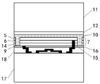
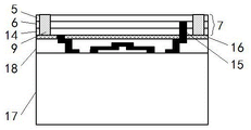
Referring to fig. 17, the ge p-i-n photodiode-based image sensor manufactured by the method of the present invention sequentially includes, from bottom to top, a silicon control and readout circuitry wafer 17, a dielectric passivation layer 16, a ge photodiode layer 7, an anti-reflection layer 19, and a lens layer 21. The germanium photodiode layer 7 is of a laminated structure and sequentially comprises a residual silicon layer 14, an undoped germanium layer 6 and a doped germanium layer 5 from bottom to top, wherein the undoped germanium layer 6 is an intrinsic layer; the residual silicon layer 14 is an n-type region, and the doped germanium layer 5 is a p-type region; in further embodiments, the remaining silicon layer 14 is a p-type region and the doped germanium layer 5 is an n-type region. The germanium photodiode layer 7 further includes an inter-trench dielectric layer 9 disposed through the stacked structure thereof, and the inter-trench dielectric layer 9 divides the germanium photodiode layer 7 into a plurality of independent pixel regions. In each pixel region, two metal connections 15 are provided from bottom to top on the dielectric passivation layer 16 and the germanium photodiode layer 7, a first metal connection being connected to the remaining silicon layer 14 and a second metal connection being connected to the doped germanium layer 5. On top of the silicon control and readout circuitry wafer 17 is an interconnect layer 18 with circuitry, the circuitry of the interconnect layer 18 being connected to the metal connections 15.
Preferably, a filter layer 20 is further provided between the antireflection layer 19 and the lens layer 21, which filter layer can selectively transmit incident light of a specific wavelength range while absorbing the remaining light.
The method for integrating the germanium p-i-n photodiode into the image sensor structure can be divided into two types according to the up-down sequence of the p-type region and the n-type region in the germanium p-i-n photodiode, and it can be understood that the basic process principles of the two types are the same. A method a (referred to as "method a") for integrating a germanium p-i-n photodiode into an image sensor structure is described in detail with reference to fig. 1 to 17.
Method a, boron doped germanium (p-type region) on top, doped germanium layer 5 being p-type region, the doping element ions implanted into the germanium being boron ions (B)+) The remaining silicon layer 14 is an n-type region. The method A comprises the following steps:
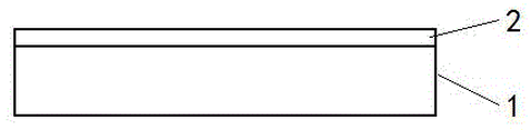
in step S1, a germanium donor wafer 1 is provided. FIG. 1 is a schematic diagram illustrating steps S1-S2. In a preferred embodiment, the germanium donor wafer 1 is cleaned and dried, and then the surface of the germanium donor wafer 1 is polished by a chemical mechanical polishing process, wherein the chemical mechanical polishing process comprises polishing the surface of the germanium donor wafer by using a polishing solution with a certain pH value; the pH value of the polishing liquid is preferably 7 to 11, and more preferably 9. During the grinding process, according to the grinding progress and the flatness of the plane of the germanium donor wafer 1, the grinding progress is controlled by adjusting the flow rate of the grinding liquid and applying a pH value adjusting liquid, wherein the pH value adjusting liquid is preferably deionized water. The chemical mechanical polishing equipment for the germanium donor wafer comprises a polishing turntable, a polishing pad, a polishing liquid nozzle and a pH value adjusting liquid nozzle, wherein the polishing turntable is used for fixing the germanium donor wafer to be polished and providing rotary power for the germanium donor wafer to be polished; the grinding pad is used for mechanically removing the surface layer of the germanium donor wafer to be ground in the relative motion with the germanium donor wafer to be ground; the grinding fluid nozzle is arranged above the grinding pad and used for injecting grinding fluid with a certain pH value onto the grinding pad; the pH value adjusting liquid nozzle is arranged close to the grinding liquid nozzle and is used for injecting the pH value adjusting liquid onto the grinding pad and mixing the pH value adjusting liquid and the grinding liquid with a certain pH value on the grinding pad to form grinding liquid with a second pH value; and the pH value adjusting liquid nozzle is also provided with a flow controller for adjusting the flow of the pH value adjusting liquid so as to adjust the second pH value to a target pH value. And flow controllers are respectively arranged on the pH value adjusting liquid nozzle and the grinding liquid nozzle and are respectively used for adjusting the flow rate of the pH value adjusting liquid and the flow rate of the grinding liquid so as to adjust the second pH value to the target pH value. The chemical mechanical polishing equipment further comprises a pH value detector for detecting the pH value of the polishing liquid on the polishing pad.
Step S1 of providing the germanium donor wafer 1 further includes depositing a layer of Plasma Enhanced Chemical Vapor Deposition (PECVD) silicon dioxide (SiO) on the germanium donor wafer 12) Film, silicon dioxide (SiO)2) The film thickness is 10nm to 90nm (nanometers) for hydrogen dissociation in the subsequent step (step S2)The surface of the germanium donor wafer 1 is protected during the sub-implantation and the silicon dioxide film can be removed after the hydrogen ion implantation. The masking film may be silicon nitride or Al2O3Or a photoresist.
Step S2, hydrogen ion (H)+) The germanium donor wafer 1 is implanted to a selected depth to determine the thickness of the germanium transfer layer 2 (i.e., the germanium film to be transferred). As shown in fig. 2.
In some embodiments, the hydrogen ion implantation may be performed by beam-line ion implantation or plasma immersion ion implantation under the following conditions: dosage range: 1X 10¹⁵Atom/cm2 ~ 1×10¹⁸Atom/cm2(preferred is>1016Atom/cm2) (ii) a Energy range: 1keV to 1MeV (typically about 50 keV); temperature range: room temperature (e.g., 25 degrees Celsius) to 600 degrees Celsius (preferred)<400 degrees celsius to minimize escape of implanted particles by diffusion); selected depth accuracy: 0.03 microns to 0.05 microns.
Optionally, a layer of amorphous germanium (a-Ge) may be deposited (e.g., by Physical Vapor Deposition (PVD)) on top of the formed region of germanium transfer layer 2. Fig. 2 is a schematic diagram showing a state after step S2.
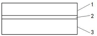
Step S3, providing a silicon target wafer 3 (n-type); preferably, the surface of the silicon target wafer is polished by using a chemical mechanical polishing process or apparatus in step S1, or by using a chemical mechanical polishing process or apparatus similar to that in step S1. FIG. 3 is a schematic diagram illustrating steps S3-S4.
If an amorphous germanium layer is deposited in step S2, it is further preferred that an amorphous germanium layer also be deposited on the surface of the silicon target wafer 3 (e.g. by physical vapour deposition), so that during the following steps S5 and S6 the combined amorphous germanium layer will be converted to crystalline germanium (c-Ge), thereby promoting bonding between the germanium donor wafer 1 and the silicon target wafer 3.
Step S4, beta bonds the surfaces of the germanium donor wafer 1 and the silicon target wafer 3. WhereinA cleaning step is performed before the beta bonding to remove the surface oxide. Performing ultrasonic cleaning on the surface of the germanium wafer by adopting acetone, methanol/ethanol and deionized water; in a preferred embodiment, deionized water and H are used2O2Further cleaning the diluent according to the proportion of (15-30): 1, preferably adopting the diluent with the proportion of 20: 1; then, deionized water and HF are used for diluting according to the dilution ratio of (30-70) to 1, preferably according to the dilution ratio of 50: 1; finally, diluted H is used according to the proportion of (15-30): 12O2The dilution is cleaned again, preferably at a 20:1 ratio. In a preferred embodiment, RCA-I solution and RCA-II solution are sequentially cleaned on the surface of a silicon wafer, followed by H2O2-H2SO4Cleaning with cleaning solution; after cleaning, the remaining liquid or particles on the wafer surface are removed with a dryer. In another embodiment, the cleaning process may be replaced by immersing the wafer in hydrofluoric acid.
The beta bonding process is also called self-bonding process, etc., and the method includes a first method or a second method, specifically for example:
method one, the low temperature bonding process, includes a low temperature thermal step that presses the cleaned and/or activated surfaces together at a moderate pressure, preferably 0.5MPa to 2.0MPa, to ensure that the injected particles (hydrogen ions or microbubbles) do not initiate fracture, or diffuse or outgas. This weak bonding is caused by electrostatic interactions (van der waals forces).
The second method is plasma cleaning activation, using Ar and N2、NH3、Ne、H2O、O2The plasma of (2) strikes the silicon target wafer 3, the plasma activates the wafer surface (creating dangling bonds on the wafer surface), and then the activated silicon target wafer 3 surface is attached to the surface of the germanium donor wafer 1, and pressure is applied to the wafer to cause self-bonding at the layer-to-layer interface.
Step S5, the germanium transfer layer 2 (bonded to the silicon target wafer 3) is separated from the germanium donor wafer 1 (i.e. delaminated using thermal, mechanical or other suitable techniques) to obtain a germanium-silicon hybrid wafer 4 (i.e. a hybrid wafer composed of the germanium transfer layer 2 and the silicon target wafer 3). Fig. 4 is a schematic diagram of step S5.
Among them, the lift-off method is, for example, a selective lift-off energy placement step, and the selective lift-off energy placement method specifically adopts an energy pulse technology, and the energy pulse is that a local (small range) energy pulse is provided, such as a heat source (e.g., laser, heating lamp), a heat source and a mechanical source, so as to realize, for example, a twist lift-off; specifically heating (e.g., heating with a heat source at about 350 degrees celsius) or cooling or differentially heating or differentially cooling one side of the substrate (germanium donor wafer 1 or silicon target wafer 4). In another embodiment, the stripping process further comprises, as an ion implantation bubble separation step, specifically, the step of introducing hydrogen ions (H)+) Implanting a germanium donor wafer 1, wherein implanted hydrogen ions capture electrons to form hydrogen, the hydrogen forms a micro-bubble layer in the bubble layer and is parallel to a cleavage plane (a crystal cleavage plane), and heating the germanium-silicon mixed wafer 4 and stripping along the cleavage plane; wherein the cleaning step and the self-bonding process can be referred to the process in beta bonding as described above.
Optionally, the separated germanium donor wafer 1 can be reused after polishing (chemical mechanical polishing (CMP)) and cleaning the surface; that is, a germanium donor wafer 1 is repeatedly used as the raw material in step S2 to form a germanium transfer layer 2 until the thickness is too thin to be used.
Step S6, completing final bonding of the sige mixed wafer 4.
The final bonding step employs the following bonding steps, for example: bonding step method one, the annealing bonding step, lasts for several hours in a process environment of less than or equal to 400 degrees celsius, preferably 3 hours in a process environment of 300 degrees celsius. Bonding step method two, apply voltage bonding step, apply voltage in order to set up the electric current through mixing the crystal defect that the crystal defect introduced in the wafer, the electric current heats and causes the bonding between the wafers, preferably use the local heating of interface (increase the series resistance) to bond.
Step S7 is to polish the surface of the germanium transfer layer 2 of the sige mixed wafer 4. The polishing is, for example, chemical mechanical polishing, and specifically, the slurry contains a mild abrasive such as borosilicate glass, titanium dioxide, titanium nitride, aluminum oxide, aluminum trioxide, ferric nitrate, cerium oxide, silicon dioxide (colloidal silica or fumed (micro powder) silica), silicon nitride, silicon carbide, graphite, diamond, and an oxidizing agent (mixed in deionized water) such as H2O2、KIO3And ferric nitrate.
Optionally, after grinding, a plasma enhanced chemical vapor deposition silicon dioxide film may be deposited on germanium transfer layer 2 on top of silicon germanium hybrid wafer 4 to protect the surface of germanium transfer layer 2 during subsequent boron ion implantation, and this silicon dioxide film may be removed after boron ion implantation.
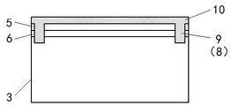
Step S8, doping element ion boron ion (B)+) The germanium transfer layer 2 on top of the sige-si hybrid wafer 4 is implanted so that the portion of the germanium transfer layer 2 near the surface is implanted with boron to form a doped ge layer 5 (p-type region) and the remaining portion (the portion near the silicon target wafer 3) is an undoped ge layer 6 (boron ions cannot reach and therefore no boron is present, being an intrinsic region). Followed by an anneal to activate the dopants. Fig. 5 is a schematic diagram of step S8. The dopants, also referred to as dopants, implants, etc., are implanted boron atoms.
Fig. 6 and 7 are schematic diagrams illustrating step S9, fig. 6 is a schematic diagram illustrating a state after step S9.1 is completed, and fig. 7 is a schematic diagram illustrating a state after step S9.3 is completed. Note that fig. 7 to 17 are each an enlarged view of a single pixel region, for example, a portion shown in fig. 6 a.
In step S9, pixel-to-pixel isolation structures are formed in the ge photodiode layer 7 to define photodiode regions (i.e., photodiode arrays, i.e., pixel regions). As shown in fig. 6, the ge photodiode layer 7 is a doped ge layer 5, an undoped ge layer 6 and a portion of the target silicon wafer 3, which are connected in sequence, i.e., a portion corresponding to the ge p-i-n photodiode layer formed in the subsequent step.
Step S9 further includes:
step S9.1, forming an isolation pattern and forming an isolation trench 8 by etching to define (divide) each pixel region; for example, if the shape of the pixel to be constituted is a square, the isolation pattern resembles a square grid; patterning the mesh using a photolithography method, and then etching to generate an isolation trench 8;
step S9.2, filling the isolation trench 8 with a flowable dielectric material (e.g., polyimide) to form an inter-trench dielectric layer 9;
step S9.3, the flowable dielectric material is excessively filled to fill the isolation trench 8 and then overflow to cover the pixel region, thereby forming the surface dielectric layer 10.
FIG. 8 is a schematic diagram illustrating steps S10-S11.
Step S10, turn over the sige mixed wafer 4.
In step S11, a carrier 11 coated with a temporary bonding agent 12 is provided. The temporary bonding adhesive 12 (temporary bonding adhesive) may be bonded or adhered by any conventional method.
Fig. 9 is a schematic diagram showing a state after completion of step S12.
Step S12, the sige mixed wafer 4 (the side with the flowable dielectric material) is temporarily bonded to the carrier 11 by the temporary bonding agent 12.
Fig. 10 is a schematic diagram showing a state after step S13 is completed.
In step S13, most of the silicon target wafer 3 (n-type) is removed by grinding (e.g., chemical mechanical grinding or etching (e.g., wet etching) or other suitable technique) to the bottom 13 of the pixel isolation. Thus, a remaining silicon layer 14 (n-type region) is formed (remains) on top of the undoped germanium layer 6, the remaining silicon layer 14, the undoped germanium layer 6 and the doped germanium layer 5, which are connected in series, together forming a germanium p-i-n photodiode layer (i.e. a germanium photodiode layer 7). The bottom 13 of the pixel isolation refers to a level corresponding to an end of the inter-trench dielectric layer 9 away from the surface dielectric layer 10, i.e., a level corresponding to a polished surface of the remaining silicon layer 14 that is retained according to requirements/process requirements.
Fig. 11 is a schematic diagram showing a state after completion of step S14.
In step S14, a dielectric passivation layer 16 is deposited on the outward facing surface of the remaining silicon layer 14.
Fig. 12 is a schematic diagram showing a state after completion of step S15.
Step S15 is to separately form metal connections 15 to the remaining silicon layer 14 (n-type region) and the doped germanium layer 5 (p-type region), respectively.
Step S15 further includes:
step S15.1, metal connection patterns are formed and vias are etched to the remaining silicon layer 14 (n-type region) and the doped germanium layer 5 (p-type region). A Barrier Metal (BM) and copper (Cu) seed are formed on the sidewalls of the via by Physical Vapor Deposition (PVD), and the via is filled by copper electrochemical deposition to form a metal connection 15.
Step S15.2, the surface is polished (e.g. chemical mechanical polishing) to remove excess copper and expose the copper pad and dielectric field, so that the metal connection 15 is flush with the dielectric passivation layer 16. Wherein the dielectric passivation layer 16 may be thinned after the chemical mechanical polishing.
At step S16, alignment marks (alignment marks) are formed on the outward-facing surface of the dielectric passivation layer 16 (by any suitable technique).
FIG. 13 is a schematic diagram illustrating steps S17-S18.
In step S17, the silicon control and readout circuitry wafer 17 is provided.
Wherein the silicon control and readout circuitry wafer 17 has control, readout and/or other suitable circuitry for the p-i-n photodiode array layer (i.e., the germanium photodiode layer 7), the surface near the outside is an interconnect layer 18 with circuitry, and the surface of the interconnect layer 18 facing the outside is the surface formed by chemical mechanical polishing of copper and barrier metal, i.e., the surface exposed with circuit metal contacts (copper pads).
And, step S17 further includes:
in step S17.1, alignment marks are formed (by any suitable technique) on the outwardly facing surface of the interconnect layer 18. This alignment mark matches the alignment mark formed on the surface of the dielectric passivation layer 16 in step S16, so that the effect of assisting alignment is achieved in the subsequent combination.
Step S18 is to interface the outward facing surface of the interconnect layer 18 of the silicon control and readout circuitry wafer 17 with the outward facing surface of the dielectric passivation layer 16 of the ge photodiode layer 7 (temporarily bonded to the carrier 11), and to connect the metal connections 15 of the ge photodiode layer 7 to the circuitry of the interconnect layer 18 by alignment marks on both to ensure alignment. And bonding, such as mixed bonding (copper-copper bonding and oxide-oxide bonding) is performed between the two. The copper-copper bonding process is a process in which the upper copper pad and the lower copper pad (the interface of the two copper portions where the metal connection 15 and the circuit of the interconnect layer 18 are butted) are connected by interdiffusion of copper during the copper grain growth.
The above alignment mark, also called an alignment mark, is a prior art. In order for the device to function, the metal connections 15 of the germanium photodiode layer 7 and the circuitry of the interconnect layer 18 of the silicon control and readout circuitry wafer 17 must be aligned with (in circuit communication with) each other. For this purpose, at least one set of alignment marks is provided, which are highly precise features and are used as a reference for the combined positioning. The alignment mark can be set according to the prior art, and therefore, the description is omitted.
Fig. 14 is a diagram illustrating a state after completion of step S18.
In step S19, annealing is performed to complete bonding. The oxide-oxide bonding process is annealing, which links the upper and lower dielectric fields (connecting interconnect layer 18 and dielectric passivation layer 16) by a dehydration condensation reaction.
In step S20, laser bond/debonding is performed to remove the carrier 11.
Fig. 15 is a diagram illustrating a state after completion of step S20.
In step S21, the surface dielectric layer 10 is removed by grinding (by, for example, chemical mechanical grinding or other suitable techniques). That is, the flowable dielectric material is removed from the surface portion of the pixel area (with the inter-trench dielectric layer 9 still present) leaving the doped germanium layer 5 exposed at the surface.
Fig. 16 is a diagram illustrating a state after completion of step S21.
In step S22, an anti-reflection layer 19 is deposited on the surface (the surface formed by the doped germanium layer 5 and the inter-trench dielectric layer 9).
In step S23, a lens layer 21 is formed on top of the antireflection layer 19.
Preferably, a filter layer 20 is also formed on top of the antireflection layer 19 and between the lens layer 21.
Fig. 17 is a schematic diagram of a state after completion of steps S22 and S23 in the preferred embodiment, that is, a structural diagram of a final product.
Method B, phosphorus doped germanium (n-type region) on top, doped germanium layer 5 being n-type region, the doping element ions implanted into the germanium being phosphorus ions (P)+) The remaining silicon layer 14 is a p-type region.
The only difference from method a is that the silicon target wafer 3 provided in step S3 is p-type, so that the remaining silicon layer 14 is a p-type region; the doping element ions implanted in step S8 are phosphorus ions (P)+) The doped germanium layer 5 is formed as an n-type region, and the remaining processes and operations are the same as those of method a.
As is well known in the art, doping a group iv element (e.g., germanium) with a group iii element (e.g., boron) forms a p-type semiconductor; doping an element of group v (e.g., phosphorus) with an element of group iv (e.g., germanium) forms an n-type semiconductor. It is therefore apparent that these similar variations are obtained by method a of the present invention described in detail above.
In conclusion, the invention realizes the high-speed, small-pixel-size and CMOS-compatible short-wave infrared image sensor (with the focal plane array) by using the low-cost and relatively simpler manufacturing process, and is suitable for industrial mass production. Meanwhile, the image sensor manufactured by the method has lower dark current from visible light to short-wave infrared wavelength and higher sensitivity. In addition, in the method of the invention, the germanium donor wafer can be recycled to generate more germanium transfer layers, so that the resource utilization rate is higher and the manufacturing cost is lower.
The above description is only for the preferred embodiment of the present invention, but the scope of the present invention is not limited thereto, and any changes or substitutions that can be easily conceived by those skilled in the art within the technical scope of the present invention are included in the scope of the present invention. It will be understood by those of ordinary skill in the art that various changes in form and details may be made therein without departing from the spirit and scope of the present invention as defined by the following claims.
Claims (12)
1. A method of integrating a germanium p-i-n photodiode into an image sensor structure, comprising the steps of:
step S1, providing a germanium donor wafer;
step S2, hydrogen ion (H)+) Implanting a germanium donor wafer to a selected depth to determine the thickness of a germanium transfer layer, the germanium transfer layer being a germanium film to be transferred;
step S3, providing a silicon target wafer;
step S4, bonding the surfaces of the germanium donor wafer and the silicon target wafer by beta;
step S5, separating the germanium transfer layer from the germanium donor wafer to obtain a germanium-silicon mixed wafer; separating the germanium transfer layer bonded and adhered on the silicon target wafer from the germanium donor wafer by using a thermal technology or a mechanical technology to obtain a mixed wafer formed by the germanium transfer layer and the silicon target wafer;
step S6, finishing the final bonding of the germanium-silicon mixed wafer;
step S7, grinding the surface of the germanium transfer layer of the germanium-silicon mixed wafer;
step S8, doping element ion boron ion (B)+) Implanting a germanium transfer layer at the top of the germanium-silicon mixed crystal dome part, implanting boron into the part of the germanium transfer layer close to the surface to form a doped germanium layer, wherein the other part close to the silicon target wafer is an undoped germanium layer;
step S9, forming a pixel-to-pixel isolation structure in the germanium photodiode layer to define a photodiode region;
step S10, turning over the germanium-silicon mixed wafer;
in step S11, a carrier coated with a temporary adhesive is provided.
2. The method of integrating a germanium p-i-n photodiode into an image sensor structure of claim 1, further comprising the step after step S11 of:
step S12, temporarily bonding/adhering the side of the germanium-silicon mixed wafer with the flowable medium material to a carrier through a temporary adhesive;
step S13, removing most of the silicon target wafer by grinding until the bottom 13 of the pixel isolation;
step S14, depositing a dielectric passivation layer on the surface of the residual silicon layer facing to the outer side;
step S15, forming metal connections separately for the residual silicon layer and the doped germanium layer;
in step S16, an alignment mark is formed on the surface of the dielectric passivation layer facing the outside.
3. The method of integrating a germanium p-i-n photodiode into an image sensor structure of claim 2, further comprising the step after step S16 of:
step S17, providing a silicon control and readout circuit wafer;
step S18, butting the outward surface of the interconnection layer of the silicon control and readout circuit wafer with the outward surface of the dielectric passivation layer of the germanium photodiode layer temporarily bonded to the carrier, and ensuring the alignment of the interconnection layer and the dielectric passivation layer through alignment marks on the interconnection layer and the dielectric passivation layer so as to connect the metal connection of the germanium photodiode layer with the circuit of the interconnection layer;
step S19, annealing to complete bonding;
step S20, carrying out laser bond/debonding and removing the carrier;
step S21, removing the surface dielectric layer by chemical mechanical polishing;
step S22, depositing an anti-reflection layer on the surface formed by the doped germanium layer and the inter-trench dielectric layer;
in step S23, a lens layer is formed on top of the anti-reflection layer.
4. The method of claim 1, wherein in step S1, the germanium donor wafer is cleaned and dried, and then the surface of the germanium donor wafer is polished by a chemical mechanical polishing process.
5. The method of claim 4, wherein the step S1 of providing the germanium donor wafer further comprises depositing a plasma enhanced chemical vapor deposition silicon dioxide film on the germanium donor wafer, the silicon dioxide film having a thickness of between 10nm and 90nm, to protect the surface of the germanium donor wafer during the subsequent step S2 of hydrogen ion implantation.
6. The method of claim 4, wherein the step of providing a germanium donor wafer of step S1 further comprises: depositing a layer of plasma enhanced chemical vapor deposition silicon dioxide film on the germanium donor wafer, wherein the thickness of the silicon dioxide film is between 10nm and 90nm, so as to protect the surface of the germanium donor wafer during the subsequent hydrogen ion implantation of step S2, and the silicon dioxide film can be removed after the hydrogen ion implantation.
7. The method of claim 1 wherein the hydrogen ion implantation in step S2 is performed by beam-line ion implantation or plasma immersion ion implantation.
8. A method of integrating a germanium p-i-n photodiode into an image sensor structure according to any one of claims 1 or 7, characterized in that an amorphous germanium layer is deposited on top of the formed germanium transfer layer region.
9. The method of claim 4 wherein the selective lift-off energy placement method uses energy pulse technology by providing localized energy pulses.
10. The method of claim 9 wherein hydrogen ions (H) are incorporated into the image sensor structure+) And implanting a germanium donor wafer, capturing electrons by the implanted hydrogen ions to form hydrogen, forming a micro bubble layer in the bubble layer by the hydrogen, parallel to the cleavage plane, heating the germanium-silicon mixed wafer, and stripping along the cleavage plane.
11. The method of claim 10, wherein the separated ge donor wafer is reusable by grinding and cleaning the surface; that is, a germanium donor wafer is repeatedly used as the raw material in step S2 to generate a germanium transfer layer until the thickness is too thin to be used.
12. The method of integrating a germanium p-i-n photodiode into an image sensor structure as claimed in any one of claims 4 or 7, wherein step S6 is performed in a final bonding of a germanium-silicon hybrid wafer, wherein the final bonding step employs an annealing bonding step, which lasts for several hours under a process environment of less than or equal to 400 degrees celsius.
Priority Applications (1)
| Application Number | Priority Date | Filing Date | Title |
|---|---|---|---|
| CN202210504638.3A CN114709233A (en) | 2022-05-10 | 2022-05-10 | Method for integrating germanium p-i-n photodiode into image sensor structure |
Applications Claiming Priority (1)
| Application Number | Priority Date | Filing Date | Title |
|---|---|---|---|
| CN202210504638.3A CN114709233A (en) | 2022-05-10 | 2022-05-10 | Method for integrating germanium p-i-n photodiode into image sensor structure |
Publications (1)
| Publication Number | Publication Date |
|---|---|
| CN114709233A true CN114709233A (en) | 2022-07-05 |
Family
ID=82176669
Family Applications (1)
| Application Number | Title | Priority Date | Filing Date |
|---|---|---|---|
| CN202210504638.3A Pending CN114709233A (en) | 2022-05-10 | 2022-05-10 | Method for integrating germanium p-i-n photodiode into image sensor structure |
Country Status (1)
| Country | Link |
|---|---|
| CN (1) | CN114709233A (en) |
-
2022
- 2022-05-10 CN CN202210504638.3A patent/CN114709233A/en active Pending
Similar Documents
| Publication | Publication Date | Title |
|---|---|---|
| JP5367562B2 (en) | Manufacturing method and structure of solar cell | |
| US8865507B2 (en) | Integrated visible and infrared imager devices and associated methods | |
| CN100442545C (en) | Method for preparing focal plane of quantum trap infrared detecter | |
| US20130168792A1 (en) | Three Dimensional Architecture Semiconductor Devices and Associated Methods | |
| US7932575B2 (en) | Method of fabricating back-illuminated imaging sensors using a bump bonding technique | |
| TW201717373A (en) | Multi-wafer based light absorption apparatus and applications thereof | |
| KR20040033276A (en) | Method and apparatus for producing ultra-thin semiconductor chip and method and apparatus for producing ultra-thin back-illuminated solid-state image pickup device | |
| JP2005514795A (en) | Photovoltaic cell and method for producing photovoltaic cell | |
| KR20140138340A (en) | Manufacture of multijunction solar cell devices | |
| CN116885040A (en) | Photodetector device and preparation method thereof | |
| US8524522B2 (en) | Microelectronic device, in particular back side illuminated image sensor, and production process | |
| CN1688014A (en) | Preparing method and application of heterobonded wafer | |
| CN217158193U (en) | Image sensor | |
| CN217158210U (en) | Image sensor manufactured based on germanium p-i-n photodiode | |
| CN114597226B (en) | Manufacturing method of image sensor based on germanium p-i-n photodiode | |
| CN217158212U (en) | Image sensor based on germanium p-i-n photodiode | |
| CN217158211U (en) | Image sensor based on germanium p-i-n photodiode | |
| CN114709233A (en) | Method for integrating germanium p-i-n photodiode into image sensor structure | |
| Fedeli et al. | Photonics and electronics integration in the HELIOS project | |
| JP2005268238A (en) | Rear surface irradiation type solid state imaging device and its manufacturing method | |
| CN113540140B (en) | Back-illuminated complementary metal oxide semiconductor image sensor and preparation method thereof | |
| KR101700724B1 (en) | Manufacture of multijunction solar cell devices | |
| US8871608B2 (en) | Method for fabricating backside-illuminated sensors | |
| CN114914261A (en) | Method for manufacturing germanium device | |
| WO2013056249A1 (en) | Three dimensional architecture semiconductor devices and associated methods |
Legal Events
| Date | Code | Title | Description |
|---|---|---|---|
| PB01 | Publication | ||
| PB01 | Publication | ||
| SE01 | Entry into force of request for substantive examination | ||
| SE01 | Entry into force of request for substantive examination |