JP5314233B2 - 制御された導電率を有する半導体材料および半導体デバイスの製造方法 - Google Patents
制御された導電率を有する半導体材料および半導体デバイスの製造方法 Download PDFInfo
- Publication number
- JP5314233B2 JP5314233B2 JP2001567026A JP2001567026A JP5314233B2 JP 5314233 B2 JP5314233 B2 JP 5314233B2 JP 2001567026 A JP2001567026 A JP 2001567026A JP 2001567026 A JP2001567026 A JP 2001567026A JP 5314233 B2 JP5314233 B2 JP 5314233B2
- Authority
- JP
- Japan
- Prior art keywords
- semiconductor material
- barrier layer
- reactor
- gas
- passivation
- Prior art date
- Legal status (The legal status is an assumption and is not a legal conclusion. Google has not performed a legal analysis and makes no representation as to the accuracy of the status listed.)
- Expired - Lifetime
Links
Images

Classifications
-
- H—ELECTRICITY
- H01—ELECTRIC ELEMENTS
- H01L—SEMICONDUCTOR DEVICES NOT COVERED BY CLASS H10
- H01L33/00—Semiconductor devices with at least one potential-jump barrier or surface barrier specially adapted for light emission; Processes or apparatus specially adapted for the manufacture or treatment thereof or of parts thereof; Details thereof
- H01L33/02—Semiconductor devices with at least one potential-jump barrier or surface barrier specially adapted for light emission; Processes or apparatus specially adapted for the manufacture or treatment thereof or of parts thereof; Details thereof characterised by the semiconductor bodies
- H01L33/26—Materials of the light emitting region
- H01L33/30—Materials of the light emitting region containing only elements of group III and group V of the periodic system
- H01L33/32—Materials of the light emitting region containing only elements of group III and group V of the periodic system containing nitrogen
- H01L33/325—Materials of the light emitting region containing only elements of group III and group V of the periodic system containing nitrogen characterised by the doping materials
-
- H—ELECTRICITY
- H01—ELECTRIC ELEMENTS
- H01L—SEMICONDUCTOR DEVICES NOT COVERED BY CLASS H10
- H01L21/00—Processes or apparatus adapted for the manufacture or treatment of semiconductor or solid state devices or of parts thereof
- H01L21/02—Manufacture or treatment of semiconductor devices or of parts thereof
- H01L21/04—Manufacture or treatment of semiconductor devices or of parts thereof the devices having at least one potential-jump barrier or surface barrier, e.g. PN junction, depletion layer or carrier concentration layer
- H01L21/18—Manufacture or treatment of semiconductor devices or of parts thereof the devices having at least one potential-jump barrier or surface barrier, e.g. PN junction, depletion layer or carrier concentration layer the devices having semiconductor bodies comprising elements of Group IV of the Periodic System or AIIIBV compounds with or without impurities, e.g. doping materials
- H01L21/30—Treatment of semiconductor bodies using processes or apparatus not provided for in groups H01L21/20 - H01L21/26
- H01L21/322—Treatment of semiconductor bodies using processes or apparatus not provided for in groups H01L21/20 - H01L21/26 to modify their internal properties, e.g. to produce internal imperfections
- H01L21/3228—Treatment of semiconductor bodies using processes or apparatus not provided for in groups H01L21/20 - H01L21/26 to modify their internal properties, e.g. to produce internal imperfections of AIIIBV compounds, e.g. to make them semi-insulating
-
- H—ELECTRICITY
- H01—ELECTRIC ELEMENTS
- H01L—SEMICONDUCTOR DEVICES NOT COVERED BY CLASS H10
- H01L21/00—Processes or apparatus adapted for the manufacture or treatment of semiconductor or solid state devices or of parts thereof
- H01L21/02—Manufacture or treatment of semiconductor devices or of parts thereof
- H01L21/02104—Forming layers
- H01L21/02365—Forming inorganic semiconducting materials on a substrate
- H01L21/02367—Substrates
- H01L21/0237—Materials
- H01L21/0242—Crystalline insulating materials
-
- H—ELECTRICITY
- H01—ELECTRIC ELEMENTS
- H01L—SEMICONDUCTOR DEVICES NOT COVERED BY CLASS H10
- H01L21/00—Processes or apparatus adapted for the manufacture or treatment of semiconductor or solid state devices or of parts thereof
- H01L21/02—Manufacture or treatment of semiconductor devices or of parts thereof
- H01L21/02104—Forming layers
- H01L21/02365—Forming inorganic semiconducting materials on a substrate
- H01L21/02436—Intermediate layers between substrates and deposited layers
- H01L21/02439—Materials
- H01L21/02455—Group 13/15 materials
- H01L21/02458—Nitrides
-
- H—ELECTRICITY
- H01—ELECTRIC ELEMENTS
- H01L—SEMICONDUCTOR DEVICES NOT COVERED BY CLASS H10
- H01L21/00—Processes or apparatus adapted for the manufacture or treatment of semiconductor or solid state devices or of parts thereof
- H01L21/02—Manufacture or treatment of semiconductor devices or of parts thereof
- H01L21/02104—Forming layers
- H01L21/02365—Forming inorganic semiconducting materials on a substrate
- H01L21/02518—Deposited layers
- H01L21/02521—Materials
- H01L21/02538—Group 13/15 materials
- H01L21/0254—Nitrides
-
- H—ELECTRICITY
- H01—ELECTRIC ELEMENTS
- H01L—SEMICONDUCTOR DEVICES NOT COVERED BY CLASS H10
- H01L21/00—Processes or apparatus adapted for the manufacture or treatment of semiconductor or solid state devices or of parts thereof
- H01L21/02—Manufacture or treatment of semiconductor devices or of parts thereof
- H01L21/02104—Forming layers
- H01L21/02365—Forming inorganic semiconducting materials on a substrate
- H01L21/02612—Formation types
- H01L21/02617—Deposition types
- H01L21/0262—Reduction or decomposition of gaseous compounds, e.g. CVD
-
- H—ELECTRICITY
- H01—ELECTRIC ELEMENTS
- H01L—SEMICONDUCTOR DEVICES NOT COVERED BY CLASS H10
- H01L21/00—Processes or apparatus adapted for the manufacture or treatment of semiconductor or solid state devices or of parts thereof
- H01L21/02—Manufacture or treatment of semiconductor devices or of parts thereof
- H01L21/02104—Forming layers
- H01L21/02365—Forming inorganic semiconducting materials on a substrate
- H01L21/02656—Special treatments
- H01L21/02664—Aftertreatments
-
- H—ELECTRICITY
- H01—ELECTRIC ELEMENTS
- H01L—SEMICONDUCTOR DEVICES NOT COVERED BY CLASS H10
- H01L33/00—Semiconductor devices with at least one potential-jump barrier or surface barrier specially adapted for light emission; Processes or apparatus specially adapted for the manufacture or treatment thereof or of parts thereof; Details thereof
- H01L33/44—Semiconductor devices with at least one potential-jump barrier or surface barrier specially adapted for light emission; Processes or apparatus specially adapted for the manufacture or treatment thereof or of parts thereof; Details thereof characterised by the coatings, e.g. passivation layer or anti-reflective coating
Landscapes
- Engineering & Computer Science (AREA)
- Manufacturing & Machinery (AREA)
- Computer Hardware Design (AREA)
- Microelectronics & Electronic Packaging (AREA)
- Power Engineering (AREA)
- Physics & Mathematics (AREA)
- Condensed Matter Physics & Semiconductors (AREA)
- General Physics & Mathematics (AREA)
- Led Devices (AREA)
- Drying Of Semiconductors (AREA)
- Junction Field-Effect Transistors (AREA)
- Bipolar Transistors (AREA)
Description
(発明の分野)
本発明は、ドーパントパッシベーション(dopant passivation)の影響を受ける、ドープされた半導体材料において所望の導電率を達成するための方法に関する。特に、本発明は、半導体成長プロセス中のドーピング種(species)パッシベーションを防止しまたは低減し、その場所または他の場所でのアニーリング工程の必要性を除く、パッシベーションバリア層の製造方法を教示する。
半導体材料は、発光ダイオード(LED)、レーザダイオード(LD)、および他の光電子および電子デバイスの製造には欠くことができない。材料の電気的および光学的特性が、組成および構造変化によって制御することができるためである。この制御を達成するために、不必要な不純物のない半導体材料を製造することが重要である。窒化ガリウム(GaN)は、青、紫、および紫外線(UV)LEDおよびLD、ならびに他の電子デバイスへの適用に関して、最も有望な半導体材料の1つである。
本発明は、水素原子によるドーピング種のパッシベーションを受けた、ドープされた半導体材料における所望の導電率を達成する新規な方法に提供する。パッシベーションは、ドーピング種に関連して半導体材料に組み込まれた水素によって引き起こされる。
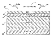
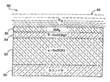
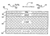
本発明は、原子水素によって半導体材料におけるドーパント種のパッシベーションを防ぐ新規な方法である。半導体材料の成長直後で、反応装置冷却の前または冷却の間に、または半導体材料の成長温度より低い温度で、バリア層を成長させる。バリア層は、半導体への水素の拡散に対する濃度の高いバリアとして機能する。また、バリア層は、化学的に水素を結合するゲッタリング層として働く。両方の場合、ドーピング種のパッシベーションが防止されるかまたは低減される。反応装置冷却に続いて、材料のさらなる処理の前に、バリア層は、エッチングなどの既知の処理によって取り除かれる。
Claims (10)
- 半導体材料におけるアクセプタおよびドナー種のパッシベーションを前記半導体材料の成長後に低減する方法であって、
成長温度の反応装置(10)内で前記半導体材料(30、50)を成長させることと、 成長ソースガスを排気することと、
前記成長ソースガスの排気後であって、かつ、前記反応装置の冷却前又は冷却中に、前記半導体材料が前記反応装置(10)にある間に、前記半導体材料(30、50)上にパッシベーションバリア層(32)を堆積することとを備え、
ここで前記パッシベーションバリア層は、前記半導体材料(30、50)内に捕らえられた水素を化学的に結合し、水素が前記半導体材料中へ拡散することを防止することができることを特徴とする方法。
- 前記パッシベーションバリア層(32、52)は、有機金属化学的気相蒸着法、プラズマ化学的気相蒸着法、ホットフィラメント化学的気相蒸着法または物理的気相蒸着法によって堆積されることを特徴とする請求項1に記載の方法。
- 前記パッシベーションバリア層(32、52)は、Si、Ge、MgOx、MgNx、ZnO、SiNx、SiOx及びこれらの混合物から選択されたものであるからなることを特徴とする請求項1に記載の方法。
- 前記パッシベーションバリア層(32、52)は、少なくとも2つの層を備え、各々の前記層は、Si、Ge、MgOx、ZnO、SiNx、MgNx、SiOx及びこれらの混合物から選択されたものから作られることを特徴とする請求項1に記載の方法。
- 前記パッシベーションバリア層(32、52)は、ゲッタリング層であり、前記ゲッタリング層が、前記半導体材料(30、50)内に捕らえられた水素を化学的に結合し、前記半導体材料(30、50)内への水素の拡散を遮断することを特徴とする請求項1に記載の方法。
- 前記ゲッタリング層(32、52)は、水素とアクセプタまたはドナー材料との間の結合エネルギーより高い、水素原子との結合エネルギーを有する成分を含むことを特徴とする請求項5に記載の方法。
- 前記反応装置(10)は、前記パッシベーションバリア層(32、52)の形成後に雰囲気ガスを含み、前記雰囲気ガスは、非反応性ガス(29)であることを特徴とする請求項1に記載の方法。
- 前記反応装置(10)は、前記パッシベーションバリア層の形成後に雰囲気ガスを含み、前記雰囲気ガスは、反応性ガスであることを特徴とする請求項1に記載の方法。
- 反応装置において半導体材料(30、50)におけるアクセプタおよびドナー種のパッシベーションを前記半導体材料の成長後に低減する方法であって、
前記半導体材料(30、50)の成長のために、前記反応装置(10)内に有機金属化合物を含むキャリアガス(16)及び窒素を含むガス(26)を流すことと、
前記窒素を含むガス(26)のフローを維持したまま、前記有機金属化合物を含むキャリアガス(16)のフローを停止することと、
有機金属化合物を含むキャリアガス(16)及び窒素を含むガス(26)を排気することと、
有機金属化合物を含むキャリアガス(16)及び窒素を含むガス(26)の排気後であって、かつ、前記反応装置の冷却前又は冷却中に、パッシベーションバリア層キャリアガス(16)を前記反応装置(10)内に噴射して、前記半導体材料(30、50)上にパッシベーションバリア層を堆積することと、ここで、前記パッシベーションバリア層(32、52)は、ゲッタリング層であり、前記ゲッタリング層が、前記半導体材料(30、50)内に捕らえられた水素を化学的に結合し、前記半導体材料(30、50)内への水素の拡散を遮断し、
前記反応装置の冷却後に前記パッシベーションバリア層(32、52)を取り除いて、前記半導体材料(30、50)をさらに処理することと
を備えたことを特徴とする方法。
- 半導体材料におけるアクセプタおよびドナー種のパッシベーションを前記半導体材料の成長後に低減する方法であって、
前記半導体材料の成長に使用した成長ソースガスを排気することと、
前記成長ソースガスの排気後であって、かつ、前記反応装置の冷却前又は冷却中に、MOCVD反応装置(10)内で前記半導体材料(30、50)上に不活性パッシベーションバリア層(32、52)を堆積することと、
前記不活性パッシベーションバリア層(32、52)の堆積中又は堆積後に、前記反応装置(10)を冷却することとを備え、
ここで前記パッシベーションバリア層は、前記半導体材料(30、50)内に捕らえられた水素を化学的に結合し、水素が前記半導体材料中へ拡散することを防止することができることを特徴とする方法。
Applications Claiming Priority (5)
| Application Number | Priority Date | Filing Date | Title |
|---|---|---|---|
| US18963000P | 2000-03-14 | 2000-03-14 | |
| US60/189,630 | 2000-03-14 | ||
| US09/644,875 US6498111B1 (en) | 2000-08-23 | 2000-08-23 | Fabrication of semiconductor materials and devices with controlled electrical conductivity |
| US09/644,875 | 2000-08-23 | ||
| PCT/US2001/007976 WO2001069659A2 (en) | 2000-03-14 | 2001-03-13 | Fabrication of semiconductor materials and devices with controlled electrical conductivity |
Publications (3)
| Publication Number | Publication Date |
|---|---|
| JP2004528700A JP2004528700A (ja) | 2004-09-16 |
| JP2004528700A5 JP2004528700A5 (ja) | 2005-01-20 |
| JP5314233B2 true JP5314233B2 (ja) | 2013-10-16 |
Family
ID=26885351
Family Applications (1)
| Application Number | Title | Priority Date | Filing Date |
|---|---|---|---|
| JP2001567026A Expired - Lifetime JP5314233B2 (ja) | 2000-03-14 | 2001-03-13 | 制御された導電率を有する半導体材料および半導体デバイスの製造方法 |
Country Status (9)
| Country | Link |
|---|---|
| EP (1) | EP1269520A2 (ja) |
| JP (1) | JP5314233B2 (ja) |
| KR (1) | KR100923937B1 (ja) |
| CN (1) | CN100559619C (ja) |
| AU (1) | AU2001243606A1 (ja) |
| CA (1) | CA2402662C (ja) |
| MY (1) | MY126104A (ja) |
| TW (1) | TWI238541B (ja) |
| WO (1) | WO2001069659A2 (ja) |
Families Citing this family (10)
| Publication number | Priority date | Publication date | Assignee | Title |
|---|---|---|---|---|
| NL1022021C2 (nl) * | 2002-11-28 | 2004-06-02 | Univ Eindhoven Tech | Werkwijze ter vorming van vacatures in een III-V-halfgeleider, een op GaN gebaseerde structuur, en de toepassing hiervan. |
| KR101008285B1 (ko) | 2005-10-28 | 2011-01-13 | 주식회사 에피밸리 | 3족 질화물 반도체 발광소자 |
| KR100742988B1 (ko) * | 2005-11-25 | 2007-07-26 | (주)더리즈 | p형 질화갈륨계 디바이스 제조방법 |
| JP2009130316A (ja) * | 2007-11-28 | 2009-06-11 | Panasonic Corp | 窒化物半導体装置およびその製造方法 |
| KR100941877B1 (ko) * | 2008-04-25 | 2010-02-11 | 김화민 | 패시배이션 조성물과 이를 이용한 스퍼터링 타겟과패시배이션막 및 그 제조방법 |
| FR3026558B1 (fr) * | 2014-09-26 | 2018-03-09 | Commissariat A L'energie Atomique Et Aux Energies Alternatives | Procede d'activation de dopants dans une couche semi-conductrice a base de gan |
| CN104377547B (zh) * | 2014-11-19 | 2017-07-21 | 北京工业大学 | 一种GaN基HEMT和LD单片集成的直接调制半导体激光器结构及其生长过程 |
| TWI548000B (zh) * | 2014-12-22 | 2016-09-01 | 力晶科技股份有限公司 | 半導體元件及其製作方法 |
| CN109285774B (zh) * | 2018-09-12 | 2023-03-24 | 江苏能华微电子科技发展有限公司 | 一种基于氮化镓的结势垒肖特基二极管及其形成方法 |
| WO2021248415A1 (zh) * | 2020-06-11 | 2021-12-16 | 苏州晶湛半导体有限公司 | 半导体结构及其制作方法 |
Family Cites Families (14)
| Publication number | Priority date | Publication date | Assignee | Title |
|---|---|---|---|---|
| JPH0653550A (ja) * | 1992-07-31 | 1994-02-25 | Toshiba Corp | 多波長光半導体整列素子 |
| JP3244980B2 (ja) * | 1995-01-06 | 2002-01-07 | 株式会社東芝 | 半導体素子の製造方法 |
| JP3325713B2 (ja) * | 1994-08-22 | 2002-09-17 | ローム株式会社 | 半導体発光素子の製法 |
| JP2872096B2 (ja) * | 1996-01-19 | 1999-03-17 | 日本電気株式会社 | 低抵抗p型窒化ガリウム系化合物半導体の気相成長方法 |
| JP3361964B2 (ja) * | 1996-09-10 | 2003-01-07 | 株式会社東芝 | 半導体発光素子およびその製造方法 |
| JP3326371B2 (ja) * | 1996-10-21 | 2002-09-24 | 東芝電子エンジニアリング株式会社 | 化合物半導体装置の製造方法 |
| US5930656A (en) * | 1996-10-21 | 1999-07-27 | Kabushiki Kaisha Toshiba | Method of fabricating a compound semiconductor device |
| JP3463524B2 (ja) * | 1997-08-04 | 2003-11-05 | 松下電器産業株式会社 | 窒化ガリウム系化合物半導体薄膜の製造方法 |
| US5926726A (en) * | 1997-09-12 | 1999-07-20 | Sdl, Inc. | In-situ acceptor activation in group III-v nitride compound semiconductors |
| JP3509514B2 (ja) * | 1997-11-13 | 2004-03-22 | 豊田合成株式会社 | 窒化ガリウム系化合物半導体の製造方法 |
| JP2000058462A (ja) * | 1998-08-13 | 2000-02-25 | Sony Corp | 窒化物系iii−v族化合物半導体の製造方法 |
| JP3987985B2 (ja) * | 1999-04-30 | 2007-10-10 | サンケン電気株式会社 | 半導体装置の製造方法 |
| JP3833848B2 (ja) * | 1999-05-10 | 2006-10-18 | パイオニア株式会社 | 3族窒化物半導体素子製造方法 |
| JP4162385B2 (ja) * | 2000-03-02 | 2008-10-08 | 株式会社リコー | p型III族窒化物半導体の製造方法 |
-
2001
- 2001-03-13 AU AU2001243606A patent/AU2001243606A1/en not_active Abandoned
- 2001-03-13 JP JP2001567026A patent/JP5314233B2/ja not_active Expired - Lifetime
- 2001-03-13 WO PCT/US2001/007976 patent/WO2001069659A2/en active Application Filing
- 2001-03-13 EP EP01916604A patent/EP1269520A2/en not_active Ceased
- 2001-03-13 CN CNB018094562A patent/CN100559619C/zh not_active Expired - Lifetime
- 2001-03-13 KR KR1020027012087A patent/KR100923937B1/ko active IP Right Grant
- 2001-03-13 CA CA2402662A patent/CA2402662C/en not_active Expired - Lifetime
- 2001-03-14 MY MYPI20011181A patent/MY126104A/en unknown
- 2001-04-16 TW TW090105940A patent/TWI238541B/zh not_active IP Right Cessation
Also Published As
| Publication number | Publication date |
|---|---|
| MY126104A (en) | 2006-09-29 |
| CN100559619C (zh) | 2009-11-11 |
| CA2402662C (en) | 2012-06-12 |
| WO2001069659A2 (en) | 2001-09-20 |
| TWI238541B (en) | 2005-08-21 |
| KR20020079955A (ko) | 2002-10-19 |
| AU2001243606A1 (en) | 2001-09-24 |
| WO2001069659A3 (en) | 2002-02-21 |
| JP2004528700A (ja) | 2004-09-16 |
| KR100923937B1 (ko) | 2009-10-29 |
| CN1443373A (zh) | 2003-09-17 |
| EP1269520A2 (en) | 2003-01-02 |
| CA2402662A1 (en) | 2001-09-20 |
Similar Documents
| Publication | Publication Date | Title |
|---|---|---|
| US6620709B2 (en) | Fabrication of semiconductor materials and devices with controlled electrical conductivity | |
| US5926726A (en) | In-situ acceptor activation in group III-v nitride compound semiconductors | |
| JP4757441B2 (ja) | 通常の低温核生成層なしでのミスマッチした基板上におけるiii族窒化物フィルムの成長 | |
| TWI651767B (zh) | 形成應力鬆弛緩衝層的方法 | |
| US20110244663A1 (en) | Forming a compound-nitride structure that includes a nucleation layer | |
| US5902393A (en) | Method for growing p-type gallium nitride based compound semiconductors by vapor phase epitaxy | |
| US20110081771A1 (en) | Multichamber split processes for led manufacturing | |
| EP0497350A1 (en) | Crystal growth method for gallium nitride-based compound semiconductor | |
| TW201101531A (en) | MOCVD single chamber split process for LED manufacturing | |
| KR20020093922A (ko) | Ⅲ족 질화물계 화합물 반도체 소자의 제조 방법 | |
| TW201106502A (en) | Cluster tool for LEDs | |
| JPH06177062A (ja) | 希土類ドープ半導体層の形成方法 | |
| KR20150007350A (ko) | Iii족 질화물 반도체 필름을 증착하는 방법 | |
| US5930656A (en) | Method of fabricating a compound semiconductor device | |
| JP5314233B2 (ja) | 制御された導電率を有する半導体材料および半導体デバイスの製造方法 | |
| KR101657915B1 (ko) | 질화 알루미늄층의 증착 방법 | |
| CN114093753B (zh) | 氮化铝单晶衬底的表面处理方法及紫外发光二极管的制备方法 | |
| JP3326371B2 (ja) | 化合物半導体装置の製造方法 | |
| JP2812375B2 (ja) | 窒化ガリウム系化合物半導体の成長方法 | |
| KR20210107098A (ko) | 증발 및 열화가 감소된 반도체 필름의 처리 방법 | |
| CN113053731B (zh) | 镓金属薄膜的制作方法以及氮化镓衬底的保护方法 | |
| JP3592922B2 (ja) | 化合物半導体基板 | |
| JP3376849B2 (ja) | 半導体薄膜の製造方法 | |
| CN113053731A (zh) | 镓金属薄膜的制作方法以及氮化镓衬底的保护方法 | |
| Feingold et al. | Rapid thermal low-pressure metal-organic chemical vapor deposition (RT-LPMOCVD) of semiconductor, dielectric and metal film onto InP and related materials |
Legal Events
| Date | Code | Title | Description |
|---|---|---|---|
| A521 | Written amendment |
Free format text: JAPANESE INTERMEDIATE CODE: A523 Effective date: 20040723 |
|
| A621 | Written request for application examination |
Free format text: JAPANESE INTERMEDIATE CODE: A621 Effective date: 20070626 |
|
| RD04 | Notification of resignation of power of attorney |
Free format text: JAPANESE INTERMEDIATE CODE: A7424 Effective date: 20070626 |
|
| A977 | Report on retrieval |
Free format text: JAPANESE INTERMEDIATE CODE: A971007 Effective date: 20100823 |
|
| A131 | Notification of reasons for refusal |
Free format text: JAPANESE INTERMEDIATE CODE: A131 Effective date: 20100907 |
|
| RD03 | Notification of appointment of power of attorney |
Free format text: JAPANESE INTERMEDIATE CODE: A7423 Effective date: 20101015 |
|
| RD04 | Notification of resignation of power of attorney |
Free format text: JAPANESE INTERMEDIATE CODE: A7424 Effective date: 20101019 |
|
| A521 | Written amendment |
Free format text: JAPANESE INTERMEDIATE CODE: A523 Effective date: 20101207 |
|
| A02 | Decision of refusal |
Free format text: JAPANESE INTERMEDIATE CODE: A02 Effective date: 20110414 |
|
| A521 | Written amendment |
Free format text: JAPANESE INTERMEDIATE CODE: A523 Effective date: 20110815 |
|
| A521 | Written amendment |
Free format text: JAPANESE INTERMEDIATE CODE: A523 Effective date: 20110826 |
|
| A911 | Transfer to examiner for re-examination before appeal (zenchi) |
Free format text: JAPANESE INTERMEDIATE CODE: A911 Effective date: 20110901 |
|
| A912 | Re-examination (zenchi) completed and case transferred to appeal board |
Free format text: JAPANESE INTERMEDIATE CODE: A912 Effective date: 20111007 |
|
| A601 | Written request for extension of time |
Free format text: JAPANESE INTERMEDIATE CODE: A601 Effective date: 20120419 |
|
| A602 | Written permission of extension of time |
Free format text: JAPANESE INTERMEDIATE CODE: A602 Effective date: 20120424 |
|
| A601 | Written request for extension of time |
Free format text: JAPANESE INTERMEDIATE CODE: A601 Effective date: 20120521 |
|
| A602 | Written permission of extension of time |
Free format text: JAPANESE INTERMEDIATE CODE: A602 Effective date: 20120524 |
|
| A601 | Written request for extension of time |
Free format text: JAPANESE INTERMEDIATE CODE: A601 Effective date: 20121005 |
|
| A602 | Written permission of extension of time |
Free format text: JAPANESE INTERMEDIATE CODE: A602 Effective date: 20121011 |
|
| A601 | Written request for extension of time |
Free format text: JAPANESE INTERMEDIATE CODE: A601 Effective date: 20121105 |
|
| A602 | Written permission of extension of time |
Free format text: JAPANESE INTERMEDIATE CODE: A602 Effective date: 20121108 |
|
| A601 | Written request for extension of time |
Free format text: JAPANESE INTERMEDIATE CODE: A601 Effective date: 20121205 |
|
| A602 | Written permission of extension of time |
Free format text: JAPANESE INTERMEDIATE CODE: A602 Effective date: 20121210 |
|
| A521 | Written amendment |
Free format text: JAPANESE INTERMEDIATE CODE: A523 Effective date: 20130107 |
|
| A521 | Written amendment |
Free format text: JAPANESE INTERMEDIATE CODE: A523 Effective date: 20130529 |
|
| A61 | First payment of annual fees (during grant procedure) |
Free format text: JAPANESE INTERMEDIATE CODE: A61 Effective date: 20130705 |
|
| R150 | Certificate of patent or registration of utility model |
Free format text: JAPANESE INTERMEDIATE CODE: R150 Ref document number: 5314233 Country of ref document: JP Free format text: JAPANESE INTERMEDIATE CODE: R150 |
|
| R250 | Receipt of annual fees |
Free format text: JAPANESE INTERMEDIATE CODE: R250 |
|
| R250 | Receipt of annual fees |
Free format text: JAPANESE INTERMEDIATE CODE: R250 |
|
| R250 | Receipt of annual fees |
Free format text: JAPANESE INTERMEDIATE CODE: R250 |
|
| R250 | Receipt of annual fees |
Free format text: JAPANESE INTERMEDIATE CODE: R250 |
|
| R250 | Receipt of annual fees |
Free format text: JAPANESE INTERMEDIATE CODE: R250 |
|
| EXPY | Cancellation because of completion of term |