JP5169263B2 - 発光装置の製造方法及び発光装置 - Google Patents
発光装置の製造方法及び発光装置 Download PDFInfo
- Publication number
- JP5169263B2 JP5169263B2 JP2008022815A JP2008022815A JP5169263B2 JP 5169263 B2 JP5169263 B2 JP 5169263B2 JP 2008022815 A JP2008022815 A JP 2008022815A JP 2008022815 A JP2008022815 A JP 2008022815A JP 5169263 B2 JP5169263 B2 JP 5169263B2
- Authority
- JP
- Japan
- Prior art keywords
- light
- light emitting
- resin
- emitting device
- emitting element
- Prior art date
- Legal status (The legal status is an assumption and is not a legal conclusion. Google has not performed a legal analysis and makes no representation as to the accuracy of the status listed.)
- Active
Links
- 238000004519 manufacturing process Methods 0.000 title claims abstract description 45
- 229920005989 resin Polymers 0.000 claims abstract description 207
- 239000011347 resin Substances 0.000 claims abstract description 207
- 239000000758 substrate Substances 0.000 claims abstract description 74
- 239000004020 conductor Substances 0.000 claims abstract description 53
- 238000007789 sealing Methods 0.000 claims abstract description 24
- 238000000034 method Methods 0.000 claims description 62
- 238000007599 discharging Methods 0.000 claims description 20
- 239000007788 liquid Substances 0.000 claims description 18
- 230000001681 protective effect Effects 0.000 claims description 14
- 238000000605 extraction Methods 0.000 abstract description 8
- 230000031700 light absorption Effects 0.000 abstract description 6
- 239000000463 material Substances 0.000 description 26
- 239000004065 semiconductor Substances 0.000 description 19
- PCHJSUWPFVWCPO-UHFFFAOYSA-N gold Chemical compound [Au] PCHJSUWPFVWCPO-UHFFFAOYSA-N 0.000 description 9
- 238000010586 diagram Methods 0.000 description 8
- 239000003822 epoxy resin Substances 0.000 description 8
- 229920000647 polyepoxide Polymers 0.000 description 8
- 239000000919 ceramic Substances 0.000 description 7
- 229910052751 metal Inorganic materials 0.000 description 7
- 239000002184 metal Substances 0.000 description 7
- OAICVXFJPJFONN-UHFFFAOYSA-N Phosphorus Chemical compound [P] OAICVXFJPJFONN-UHFFFAOYSA-N 0.000 description 6
- 229910052737 gold Inorganic materials 0.000 description 6
- 239000010931 gold Substances 0.000 description 6
- 150000004767 nitrides Chemical class 0.000 description 6
- RYGMFSIKBFXOCR-UHFFFAOYSA-N Copper Chemical compound [Cu] RYGMFSIKBFXOCR-UHFFFAOYSA-N 0.000 description 5
- PXHVJJICTQNCMI-UHFFFAOYSA-N Nickel Chemical compound [Ni] PXHVJJICTQNCMI-UHFFFAOYSA-N 0.000 description 5
- 238000006243 chemical reaction Methods 0.000 description 5
- 229910052802 copper Inorganic materials 0.000 description 5
- 239000010949 copper Substances 0.000 description 5
- 238000009826 distribution Methods 0.000 description 5
- 229910052747 lanthanoid Inorganic materials 0.000 description 5
- 150000002602 lanthanoids Chemical class 0.000 description 5
- XEEYBQQBJWHFJM-UHFFFAOYSA-N Iron Chemical compound [Fe] XEEYBQQBJWHFJM-UHFFFAOYSA-N 0.000 description 4
- 239000010410 layer Substances 0.000 description 4
- BQCADISMDOOEFD-UHFFFAOYSA-N Silver Chemical compound [Ag] BQCADISMDOOEFD-UHFFFAOYSA-N 0.000 description 3
- 238000010521 absorption reaction Methods 0.000 description 3
- 229910052782 aluminium Inorganic materials 0.000 description 3
- 239000011521 glass Substances 0.000 description 3
- 238000000465 moulding Methods 0.000 description 3
- 238000007639 printing Methods 0.000 description 3
- 229910052761 rare earth metal Inorganic materials 0.000 description 3
- 229920002050 silicone resin Polymers 0.000 description 3
- 229910052709 silver Inorganic materials 0.000 description 3
- 239000004332 silver Substances 0.000 description 3
- 239000002356 single layer Substances 0.000 description 3
- 229910018072 Al 2 O 3 Inorganic materials 0.000 description 2
- ZOKXTWBITQBERF-UHFFFAOYSA-N Molybdenum Chemical compound [Mo] ZOKXTWBITQBERF-UHFFFAOYSA-N 0.000 description 2
- KDLHZDBZIXYQEI-UHFFFAOYSA-N Palladium Chemical compound [Pd] KDLHZDBZIXYQEI-UHFFFAOYSA-N 0.000 description 2
- 229910052784 alkaline earth metal Inorganic materials 0.000 description 2
- 150000001342 alkaline earth metals Chemical class 0.000 description 2
- 150000004645 aluminates Chemical class 0.000 description 2
- XAGFODPZIPBFFR-UHFFFAOYSA-N aluminium Chemical compound [Al] XAGFODPZIPBFFR-UHFFFAOYSA-N 0.000 description 2
- 238000005520 cutting process Methods 0.000 description 2
- 239000000428 dust Substances 0.000 description 2
- 238000010304 firing Methods 0.000 description 2
- 229910052736 halogen Inorganic materials 0.000 description 2
- 150000002367 halogens Chemical class 0.000 description 2
- 229910052742 iron Inorganic materials 0.000 description 2
- 238000005304 joining Methods 0.000 description 2
- 239000004973 liquid crystal related substance Substances 0.000 description 2
- 150000002739 metals Chemical class 0.000 description 2
- 239000000203 mixture Substances 0.000 description 2
- 229910052750 molybdenum Inorganic materials 0.000 description 2
- 239000011733 molybdenum Substances 0.000 description 2
- 230000002093 peripheral effect Effects 0.000 description 2
- BASFCYQUMIYNBI-UHFFFAOYSA-N platinum Chemical compound [Pt] BASFCYQUMIYNBI-UHFFFAOYSA-N 0.000 description 2
- -1 rare earth aluminate Chemical class 0.000 description 2
- WFKWXMTUELFFGS-UHFFFAOYSA-N tungsten Chemical compound [W] WFKWXMTUELFFGS-UHFFFAOYSA-N 0.000 description 2
- 229910052721 tungsten Inorganic materials 0.000 description 2
- 239000010937 tungsten Substances 0.000 description 2
- 229910015363 Au—Sn Inorganic materials 0.000 description 1
- BTBUEUYNUDRHOZ-UHFFFAOYSA-N Borate Chemical compound [O-]B([O-])[O-] BTBUEUYNUDRHOZ-UHFFFAOYSA-N 0.000 description 1
- 229910000906 Bronze Inorganic materials 0.000 description 1
- 229910052684 Cerium Inorganic materials 0.000 description 1
- JOYRKODLDBILNP-UHFFFAOYSA-N Ethyl urethane Chemical compound CCOC(N)=O JOYRKODLDBILNP-UHFFFAOYSA-N 0.000 description 1
- 229910052693 Europium Inorganic materials 0.000 description 1
- 229910052688 Gadolinium Inorganic materials 0.000 description 1
- 229910001030 Iron–nickel alloy Inorganic materials 0.000 description 1
- 229910052765 Lutetium Inorganic materials 0.000 description 1
- 229910000990 Ni alloy Inorganic materials 0.000 description 1
- BPQQTUXANYXVAA-UHFFFAOYSA-N Orthosilicate Chemical compound [O-][Si]([O-])([O-])[O-] BPQQTUXANYXVAA-UHFFFAOYSA-N 0.000 description 1
- 229910052581 Si3N4 Inorganic materials 0.000 description 1
- UCKMPCXJQFINFW-UHFFFAOYSA-N Sulphide Chemical compound [S-2] UCKMPCXJQFINFW-UHFFFAOYSA-N 0.000 description 1
- 229910052771 Terbium Inorganic materials 0.000 description 1
- 229910010413 TiO 2 Inorganic materials 0.000 description 1
- 229920001807 Urea-formaldehyde Polymers 0.000 description 1
- GEIAQOFPUVMAGM-UHFFFAOYSA-N ZrO Inorganic materials [Zr]=O GEIAQOFPUVMAGM-UHFFFAOYSA-N 0.000 description 1
- 229910045601 alloy Inorganic materials 0.000 description 1
- 239000000956 alloy Substances 0.000 description 1
- 229910052586 apatite Inorganic materials 0.000 description 1
- 230000005540 biological transmission Effects 0.000 description 1
- 238000005219 brazing Methods 0.000 description 1
- 239000010974 bronze Substances 0.000 description 1
- 239000003795 chemical substances by application Substances 0.000 description 1
- 239000003086 colorant Substances 0.000 description 1
- 238000000748 compression moulding Methods 0.000 description 1
- KUNSUQLRTQLHQQ-UHFFFAOYSA-N copper tin Chemical compound [Cu].[Sn] KUNSUQLRTQLHQQ-UHFFFAOYSA-N 0.000 description 1
- 239000013078 crystal Substances 0.000 description 1
- 230000006866 deterioration Effects 0.000 description 1
- 230000000694 effects Effects 0.000 description 1
- 230000005496 eutectics Effects 0.000 description 1
- 239000004744 fabric Substances 0.000 description 1
- 239000000945 filler Substances 0.000 description 1
- 239000010408 film Substances 0.000 description 1
- 239000010419 fine particle Substances 0.000 description 1
- 229910052733 gallium Inorganic materials 0.000 description 1
- 238000009413 insulation Methods 0.000 description 1
- 230000008018 melting Effects 0.000 description 1
- 238000002844 melting Methods 0.000 description 1
- 229910052759 nickel Inorganic materials 0.000 description 1
- 229910052763 palladium Inorganic materials 0.000 description 1
- 238000000059 patterning Methods 0.000 description 1
- VSIIXMUUUJUKCM-UHFFFAOYSA-D pentacalcium;fluoride;triphosphate Chemical compound [F-].[Ca+2].[Ca+2].[Ca+2].[Ca+2].[Ca+2].[O-]P([O-])([O-])=O.[O-]P([O-])([O-])=O.[O-]P([O-])([O-])=O VSIIXMUUUJUKCM-UHFFFAOYSA-D 0.000 description 1
- 239000005011 phenolic resin Substances 0.000 description 1
- 238000000206 photolithography Methods 0.000 description 1
- 239000000049 pigment Substances 0.000 description 1
- 229910052697 platinum Inorganic materials 0.000 description 1
- 229920001721 polyimide Polymers 0.000 description 1
- 239000009719 polyimide resin Substances 0.000 description 1
- 238000004382 potting Methods 0.000 description 1
- 239000000843 powder Substances 0.000 description 1
- 150000002910 rare earth metals Chemical class 0.000 description 1
- 239000003870 refractory metal Substances 0.000 description 1
- 229910052594 sapphire Inorganic materials 0.000 description 1
- 239000010980 sapphire Substances 0.000 description 1
- SBIBMFFZSBJNJF-UHFFFAOYSA-N selenium;zinc Chemical compound [Se]=[Zn] SBIBMFFZSBJNJF-UHFFFAOYSA-N 0.000 description 1
- HQVNEWCFYHHQES-UHFFFAOYSA-N silicon nitride Chemical compound N12[Si]34N5[Si]62N3[Si]51N64 HQVNEWCFYHHQES-UHFFFAOYSA-N 0.000 description 1
- 229910000679 solder Inorganic materials 0.000 description 1
- 238000005507 spraying Methods 0.000 description 1
- 238000004544 sputter deposition Methods 0.000 description 1
- 239000000126 substance Substances 0.000 description 1
- 229920005992 thermoplastic resin Polymers 0.000 description 1
- 229920001187 thermosetting polymer Polymers 0.000 description 1
- 239000010409 thin film Substances 0.000 description 1
- 238000001721 transfer moulding Methods 0.000 description 1
- 229910052723 transition metal Inorganic materials 0.000 description 1
- 238000007740 vapor deposition Methods 0.000 description 1
- 229910052727 yttrium Inorganic materials 0.000 description 1
Images


Classifications
-
- H—ELECTRICITY
- H01—ELECTRIC ELEMENTS
- H01L—SEMICONDUCTOR DEVICES NOT COVERED BY CLASS H10
- H01L2224/00—Indexing scheme for arrangements for connecting or disconnecting semiconductor or solid-state bodies and methods related thereto as covered by H01L24/00
- H01L2224/01—Means for bonding being attached to, or being formed on, the surface to be connected, e.g. chip-to-package, die-attach, "first-level" interconnects; Manufacturing methods related thereto
- H01L2224/42—Wire connectors; Manufacturing methods related thereto
- H01L2224/44—Structure, shape, material or disposition of the wire connectors prior to the connecting process
- H01L2224/45—Structure, shape, material or disposition of the wire connectors prior to the connecting process of an individual wire connector
- H01L2224/45001—Core members of the connector
- H01L2224/45099—Material
- H01L2224/451—Material with a principal constituent of the material being a metal or a metalloid, e.g. boron (B), silicon (Si), germanium (Ge), arsenic (As), antimony (Sb), tellurium (Te) and polonium (Po), and alloys thereof
- H01L2224/45138—Material with a principal constituent of the material being a metal or a metalloid, e.g. boron (B), silicon (Si), germanium (Ge), arsenic (As), antimony (Sb), tellurium (Te) and polonium (Po), and alloys thereof the principal constituent melting at a temperature of greater than or equal to 950°C and less than 1550°C
- H01L2224/45144—Gold (Au) as principal constituent
-
- H—ELECTRICITY
- H01—ELECTRIC ELEMENTS
- H01L—SEMICONDUCTOR DEVICES NOT COVERED BY CLASS H10
- H01L2224/00—Indexing scheme for arrangements for connecting or disconnecting semiconductor or solid-state bodies and methods related thereto as covered by H01L24/00
- H01L2224/01—Means for bonding being attached to, or being formed on, the surface to be connected, e.g. chip-to-package, die-attach, "first-level" interconnects; Manufacturing methods related thereto
- H01L2224/42—Wire connectors; Manufacturing methods related thereto
- H01L2224/47—Structure, shape, material or disposition of the wire connectors after the connecting process
- H01L2224/48—Structure, shape, material or disposition of the wire connectors after the connecting process of an individual wire connector
- H01L2224/481—Disposition
- H01L2224/48135—Connecting between different semiconductor or solid-state bodies, i.e. chip-to-chip
- H01L2224/48137—Connecting between different semiconductor or solid-state bodies, i.e. chip-to-chip the bodies being arranged next to each other, e.g. on a common substrate
-
- H—ELECTRICITY
- H01—ELECTRIC ELEMENTS
- H01L—SEMICONDUCTOR DEVICES NOT COVERED BY CLASS H10
- H01L2224/00—Indexing scheme for arrangements for connecting or disconnecting semiconductor or solid-state bodies and methods related thereto as covered by H01L24/00
- H01L2224/01—Means for bonding being attached to, or being formed on, the surface to be connected, e.g. chip-to-package, die-attach, "first-level" interconnects; Manufacturing methods related thereto
- H01L2224/42—Wire connectors; Manufacturing methods related thereto
- H01L2224/47—Structure, shape, material or disposition of the wire connectors after the connecting process
- H01L2224/48—Structure, shape, material or disposition of the wire connectors after the connecting process of an individual wire connector
- H01L2224/484—Connecting portions
- H01L2224/48463—Connecting portions the connecting portion on the bonding area of the semiconductor or solid-state body being a ball bond
- H01L2224/48465—Connecting portions the connecting portion on the bonding area of the semiconductor or solid-state body being a ball bond the other connecting portion not on the bonding area being a wedge bond, i.e. ball-to-wedge, regular stitch
-
- H—ELECTRICITY
- H01—ELECTRIC ELEMENTS
- H01L—SEMICONDUCTOR DEVICES NOT COVERED BY CLASS H10
- H01L2924/00—Indexing scheme for arrangements or methods for connecting or disconnecting semiconductor or solid-state bodies as covered by H01L24/00
- H01L2924/013—Alloys
- H01L2924/0132—Binary Alloys
- H01L2924/01322—Eutectic Alloys, i.e. obtained by a liquid transforming into two solid phases
-
- H—ELECTRICITY
- H01—ELECTRIC ELEMENTS
- H01L—SEMICONDUCTOR DEVICES NOT COVERED BY CLASS H10
- H01L2924/00—Indexing scheme for arrangements or methods for connecting or disconnecting semiconductor or solid-state bodies as covered by H01L24/00
- H01L2924/15—Details of package parts other than the semiconductor or other solid state devices to be connected
- H01L2924/181—Encapsulation
Description
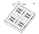
本実施の形態の発光装置200を、図2A〜図2Cに示す。図2Aは発光装置200の斜視図、図2Bは図2AのY−Y‘線における断面図、図2Cは図2Aの封止部材206を透けた状態にした上面図を示す。尚、図2Cに示すように、光反射樹脂202の角部は丸みを帯びたような形状であるが、図2Aでは簡略化のため丸みを省略してある。
第1の工程は、導体配線を有する基板上に発光素子を載置し、この発光素子と導体配線とを電気的に接続するものであり、図1Aはこの第1の工程が完了した状態を示している。図1Aに示すように、本形態において発光装置の集合体100は、基板101の上面に導体配線103A、103B、103Cが設けられている。導体配線の形状や大きさ、配置等については、図1Aに示すものに限らず、任意に選択することができる。
第2の工程は、基板上に、発光素子からの光を反射する光反射樹脂を、発光素子の周囲を取り囲むように形成するものである。
図1Bは、第1の工程で得られた発光素子載置済みの基板101上に、樹脂吐出装置1000を用いて光反射樹脂102(102A)を形成していく工程を示す図である。本実施の形態では、まず図1Bに示すように第1の光反射樹脂102Aを設け、次に図1Cに示すように第2の光反射樹脂102Bを設け、この2つの工程によって発光素子の周囲を取り囲む光反射樹脂102を設ける。
次いで、図1Cに示すように、樹脂吐出装置1000を、図中の矢印1bの方向、すなわち、先に形成した第1の光反射樹脂102Aと交差するように移動させ、発光素子104の周囲を取り囲むように第2の光反射樹脂102Bを設ける。このとき、樹脂吐出装置1000は液体樹脂を吐出ながら基板上101、導体配線103A、103B、さらには、先に形成した光反射樹脂102Aの上方を移動してもよく、或いは、光反射樹脂102Aの上方においては樹脂の吐出を中断するなどの方法をとることもできる。
第3の工程は、第2の工程で光反射樹脂を硬化した後、発光素子を被覆するよう封止部材を形成するものである。図1Eは図1Dで得られる発光装置の集合体100に、さらに封止部材106を設けた発光装置の集合体100を示す図である。この図において、封止部材106は、発光素子104の周囲を取り囲むことで枠状に形成されている光反射樹脂102の内側を充填するようにして設けられている。このようにすることで、発光素子104を塵芥や水分、また外力などから保護することができる。尚、図1Eでは、光反射樹脂102で囲まれた領域Kを充填するように封止部材106を設けているが、これに加えて、発光素子が載置されていない領域L及び領域Mなどにも設けることができる。
第4の工程は、第3の工程で形成された封止部材を硬化した後に、基板を分割して個片化し、個々の発光装置とするものである。
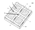
実施の形態2にかかる発光装置300を、図3に示す。図3は発光装置300の上面図を示す。
第2の工程は、基板上に、発光素子からの光を反射する光反射樹脂を、発光素子の周囲を取り囲むように形成するものである。実施の形態2においては、発光装置300は光反射樹脂が基板分割位置に形成されないように設けられており、この点が実施の形態1と異なる。用いる樹脂吐出装置は、実施の形態1と同様のものを用いる。
図4Aは、第1の工程で得られた発光素子載置済みの基板401上に、樹脂吐出装置4000を用いて光反射樹脂402(402A)を形成していく工程を示す図である。図4Aと、この後に行われる図4Bに示す工程との両方によって発光素子の周囲に光反射樹脂402を設けることができる。
図5は、第2の工程の異なる方法を説明する図である。
図6は、第2の工程の異なる方法を説明する図である。
図8Aは、樹脂吐出装置の代わりに、開口部を有するマスク8000を用いて光反射樹脂を形成する方法を説明する図である。図8Bは、図8Aのマスク8000を基板801上に配置した際の断面図であり、スキージ8030を用いて高粘度樹脂802Aを開口部8020から注入するように移動させていく状態を示している(いわゆる印刷法)。
図9は、第3の工程において封止部材を設けた後にさらにレンズ部材を設け、その後第4の工程において分割されて得られる発光装置900の断面図を示す。
基板は導体配線を配するとともに、発光素子や保護素子などが載置可能な絶縁性の略板状部材である。具体的な材料としては、セラミックス(Al2O3、AlN等)、エポキシ樹脂、ポリイミド樹脂などをあげることができる。
導体配線は、基板の上面に形成され、基板の内部や表面などを介して裏面にまで連続するよう設けられ、外部と電気的な接続が取れるような機能を有するものである。また、外部とは電気的な接続が無く、光反射材として機能する物も含む。
光反射樹脂は、発光素子からの光を効率よく反射可能な部材であり、発光素子の周囲を取り囲むように設けられる。光反射樹脂を構成する具体的な材料としては絶縁性部材が好ましく、また、発光素子からの光や、外光などが透過や吸収しにくい部材が好ましい。また、ある程度の強度を有するもので、熱硬化性樹脂、熱可塑性樹脂などを用いることができ、より具体的には、フェノール樹脂、エポキシ樹脂、BTレジンや、PPAやシリコーン樹脂などが挙げられる。これら母体となる樹脂に、発光素子からの光を吸収しにくくかつ母体となる樹脂に対して屈折率差の大きい反射部材(例えばTiO2、Al2O3、ZrO2、MgO)などの粉末を分散することで、効率よく光を反射させることができる。
封止部材は、第3の工程において、光反射樹脂で囲まれた領域やその外側に設けられるものであり、発光素子や保護素子、導電性ワイヤなどを、塵芥、水分や外力などから保護する部材である。また、発光素子からの光を透過可能な透光性を有し、且つ、それらによって劣化のしにくい耐光性を有するものが好ましい。具体的な材料としては、シリコーン樹脂、エポキシ樹脂やユリア樹脂を挙げることができる。このような材料に加え、所望に応じて着色剤、光拡散剤、フィラー、色変換部材(蛍光部材)などを含有させることもできる。
ダイボンド部材は、基体や導体配線上に発光素子や保護素子などを載置させるための接合部材であり、載置する素子の基板によって導電性ダイボンド部材又は縁性ダイボンド部材のいずれかを選択することができる。例えば、絶縁性基板であるサファイア上に窒化物半導体層を積層させた半導体発光素子の場合、ダイボンド部材は絶縁性でも導電性でも用いることができ、SiC基板などの導電性基板を用いる場合は、導電性ダイボンド部材を用いることで導通を図ることができる。絶縁性ダイボンド部材としては、エポキシ樹脂、シリコーン樹脂等を用いることができる。これらの樹脂を用いる場合は、半導体発光素子からの光や熱による劣化を考慮して、半導体発光素子裏面にAl膜などの反射率の高い金属層を設けることができる。この場合、蒸着やスパッタあるいは薄膜を接合させるなどの方法を用いることができる。また、導電性ダイボンド部材としては、銀、金、パラジウムなどの導電性ペーストや、Au−Sn共晶などの半田、低融点金属等のろう材を用いることができる。さらに、これらダイボンド部材のうち、特に透光性のダイボンド部材を用いる場合は、その中に半導体発光素子からの光を吸収して異なる波長の光を発光する蛍光部材を含有させることもできる。
発光素子の電極と、基板に設けられる導電部材とを接続する導電性ワイヤは、金、銅、白金、アルミニウム等の金属及びそれらの合金を用いた導電性ワイヤが挙げられる。特に、熱抵抗などに優れた金を用いるのが好ましい。
上記封止部材/レンズ部材中に、波長変換部材として半導体発光素子からの光の少なくとも一部を吸収して異なる波長を有する光を発する蛍光部材を含有させることもできる。
本発明においては、半導体発光素子として発光ダイオードを用いるのが好ましい。
樹脂吐出装置は、第2の工程において光反射樹脂を設ける際に用いるものであり、例えば図1Bなどに示すように、空気の圧力で液体樹脂を連続的に、或いは、ドット状に吐出可能な装置である。
200、300、900・・・発光装置
101、201、301、401、501、601、801、901・・・基板
102、102A、102B、202、302、402A、402B、502、602A、602B、602B‘、802、802A,902・・・光反射樹脂
103A、103B、103C、203A、203B、203C、303A、903A、903B・・・導体配線
104、204、304、404、804、904・・・発光素子
105、205、305、805、905・・・導電ワイヤ
106、206、906・・・封止部材
908・・・レンズ部材
1000、4000、5000、6000・・・樹脂吐出装置
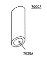
1010、4010、6010、7000A、7000B、7000C・・・ノズル
7030A、7030B、7030C・・・ノズル開口部
8000・・・マスク
8010A・・・薄板部
8010B・・・突出部
8020・・・開口部
8030・・・スキージ
Claims (12)
- 導体配線を有する基板上に発光素子を載置し、該発光素子と前記導体配線とを電気的に接続する第1の工程と、
前記基板上に、前記発光素子からの光を反射する光反射樹脂を、前記発光素子の周囲を取り囲むように形成する第2の工程と、
前記光反射樹脂を硬化後に、前記発光素子を被覆するよう封止部材を形成する第3の工程と、を有し、
前記第1の工程は、導電性ワイヤを用いて接続されており、前記第2の工程は、前記導電性ワイヤの少なくとも一部を被覆するように形成されることを特徴とする発光素子の製造方法。 - 前記光反射樹脂は、樹脂吐出装置から液体樹脂を吐出して形成される請求項1記載の発光装置の製造方法。
- 前記樹脂吐出装置は、液体樹脂を吐出ながら基板上を移動する請求項2記載の発光装置の製造方法。
- 前記第3の工程で形成される封止部材を硬化後、前記基板を分割する第4の工程を有し、
前記樹脂吐出装置は、前記第4の工程における基板の分割位置上を、液体樹脂を吐出しながら通過するよう移動する請求項2又は請求項3記載の発光装置の製造方法。 - 前記樹脂吐出装置は、前記第4の工程における基板の分割位置から離間した領域上を移動するよう移動する請求項2乃至請求項4のいずれか1つに記載の発光装置の製造方法。
- 前記樹脂吐出装置は、第1の光反射樹脂を形成するように前記基板上を縦方向又は横方向に向かって移動し、次いで、前記第1の光反射樹脂と少なくとも一部が接する第2の光反射樹脂を形成するように、前記第1の光反射樹脂の上を通過するよう移動する請求項2乃至請求項5のいずれか1つに記載の発光装置の製造方法。
- 前記樹脂吐出装置は、静止した状態で液体樹脂を吐出し、移動時には吐出を中断する請求項1又は請求項2記載の発光装置の製造方法。
- 前記第1の光反射樹脂と前記第2の光反射樹脂は、前記第4の工程における分割位置から離間した位置で接するように形成される請求項6又は請求項7記載の発光装置の製造方法。
- 前記光反射樹脂は、前記発光素子の上部を被覆するとともにその周辺に開口部を有するマスクを用い、該開口部から光反射樹脂を注入して形成する請求項1記載の発光装置の製造方法。
- 前記第1の工程は、保護素子を載置し、前記導体配線と該保護素子とを電気的に接続する工程を含み、
前記第2の工程は、前記保護素子を被覆するように形成される請求項1乃至請求項9のいずれか1つに記載の発光装置の製造方法。 - 前記第1の光反射樹脂と第2の光反射樹脂は、前記保護素子の上部で重なるように形成される請求項10記載の発光装置の製造方法。
- 請求項1乃至請求項11のいずれか1つの製造方法によって得られる発光装置。
Priority Applications (5)
| Application Number | Priority Date | Filing Date | Title |
|---|---|---|---|
| JP2008022815A JP5169263B2 (ja) | 2008-02-01 | 2008-02-01 | 発光装置の製造方法及び発光装置 |
| US12/341,189 US8049237B2 (en) | 2007-12-28 | 2008-12-22 | Light emitting device |
| US13/242,641 US9024343B2 (en) | 2007-12-28 | 2011-09-23 | Light emitting device |
| US14/610,030 US9806234B2 (en) | 2007-12-28 | 2015-01-30 | Light emitting device |
| US15/784,781 US10559721B2 (en) | 2007-12-28 | 2017-10-16 | Light emitting device |
Applications Claiming Priority (1)
| Application Number | Priority Date | Filing Date | Title |
|---|---|---|---|
| JP2008022815A JP5169263B2 (ja) | 2008-02-01 | 2008-02-01 | 発光装置の製造方法及び発光装置 |
Publications (3)
| Publication Number | Publication Date |
|---|---|
| JP2009182307A JP2009182307A (ja) | 2009-08-13 |
| JP2009182307A5 JP2009182307A5 (ja) | 2011-03-10 |
| JP5169263B2 true JP5169263B2 (ja) | 2013-03-27 |
Family
ID=41036003
Family Applications (1)
| Application Number | Title | Priority Date | Filing Date |
|---|---|---|---|
| JP2008022815A Active JP5169263B2 (ja) | 2007-12-28 | 2008-02-01 | 発光装置の製造方法及び発光装置 |
Country Status (1)
| Country | Link |
|---|---|
| JP (1) | JP5169263B2 (ja) |
Cited By (1)
| Publication number | Priority date | Publication date | Assignee | Title |
|---|---|---|---|---|
| US9698321B2 (en) | 2015-08-31 | 2017-07-04 | Panasonic Intellectual Property Management Co., Ltd. | Light-emitting apparatus, illumination apparatus, and method of manufacturing light-emitting apparatus |
Families Citing this family (34)
| Publication number | Priority date | Publication date | Assignee | Title |
|---|---|---|---|---|
| JP5396215B2 (ja) * | 2009-09-24 | 2014-01-22 | スタンレー電気株式会社 | 半導体発光装置の製造方法、半導体発光装置および液晶表示装置 |
| JP5757687B2 (ja) * | 2010-02-09 | 2015-07-29 | シャープ株式会社 | 発光装置、面光源装置、液晶表示装置、および発光装置の製造方法 |
| BR112012026371B1 (pt) | 2010-04-16 | 2020-12-15 | Nichia Corporation | Dispositivo emissor de luz e método para a sua fabricação |
| DE102010028407B4 (de) * | 2010-04-30 | 2021-01-14 | OSRAM Opto Semiconductors Gesellschaft mit beschränkter Haftung | Optoelektronisches Bauelement und Verfahren zum Herstellen eines optoelektronischen Bauelements |
| JP5481277B2 (ja) | 2010-06-04 | 2014-04-23 | シャープ株式会社 | 発光装置 |
| JP5810302B2 (ja) * | 2010-06-28 | 2015-11-11 | パナソニックIpマネジメント株式会社 | 発光装置、バックライトユニット、液晶表示装置及び照明装置 |
| DE102010031945A1 (de) * | 2010-07-22 | 2012-01-26 | Osram Opto Semiconductors Gmbh | Halbleiterbauelement und Verfahren zur Herstellung eines Halbleiterbauelements |
| JP5703663B2 (ja) * | 2010-09-30 | 2015-04-22 | 日亜化学工業株式会社 | 発光装置および発光装置の製造方法 |
| JP5648422B2 (ja) * | 2010-10-29 | 2015-01-07 | 日亜化学工業株式会社 | 発光装置及びその製造方法 |
| EP2448028B1 (en) | 2010-10-29 | 2017-05-31 | Nichia Corporation | Light emitting apparatus and production method thereof |
| JP2012099544A (ja) * | 2010-10-29 | 2012-05-24 | Nichia Chem Ind Ltd | 発光装置の製造方法 |
| TWI554811B (zh) | 2011-04-20 | 2016-10-21 | Panasonic Ip Man Co Ltd | A light-emitting device, a backlight unit, a liquid crystal display device, a lighting device, and a light-emitting device manufacturing method |
| JP5699838B2 (ja) | 2011-07-14 | 2015-04-15 | 豊田合成株式会社 | 発光装置の製造方法 |
| CN103258920A (zh) * | 2012-02-17 | 2013-08-21 | 展晶科技(深圳)有限公司 | 发光二极管封装结构的制造方法 |
| WO2014038169A1 (ja) * | 2012-09-06 | 2014-03-13 | シャープ株式会社 | 発光素子基板およびその製造方法 |
| JP5444588B2 (ja) * | 2012-09-14 | 2014-03-19 | スタンレー電気株式会社 | 半導体発光装置の製造方法 |
| JP5625224B2 (ja) * | 2013-07-29 | 2014-11-19 | スタンレー電気株式会社 | 半導体発光装置 |
| US9461214B2 (en) | 2013-11-29 | 2016-10-04 | Nichia Corporation | Light emitting device with phosphor layer |
| JP5843900B2 (ja) * | 2014-02-17 | 2016-01-13 | シャープ株式会社 | 発光装置 |
| JP6583764B2 (ja) | 2014-09-12 | 2019-10-02 | パナソニックIpマネジメント株式会社 | 発光装置、及び照明装置 |
| JP6256700B2 (ja) | 2014-11-11 | 2018-01-10 | 豊田合成株式会社 | 発光装置 |
| JP6572540B2 (ja) * | 2014-12-26 | 2019-09-11 | 日亜化学工業株式会社 | パッケージ、発光装置およびその製造方法 |
| JP2015149515A (ja) * | 2015-05-28 | 2015-08-20 | シャープ株式会社 | 発光装置および照明機器 |
| JP6729025B2 (ja) | 2016-06-14 | 2020-07-22 | 日亜化学工業株式会社 | 発光装置 |
| JP2019071352A (ja) * | 2017-10-10 | 2019-05-09 | シチズン電子株式会社 | 照明装置とその製造方法 |
| JP7037046B2 (ja) | 2018-01-31 | 2022-03-16 | 日亜化学工業株式会社 | 発光装置及びその製造方法 |
| JP7323763B2 (ja) | 2018-12-27 | 2023-08-09 | 日亜化学工業株式会社 | 発光装置及び発光装置の製造方法 |
| JP7240907B2 (ja) * | 2019-03-12 | 2023-03-16 | シチズン電子株式会社 | 発光装置及び発光装置の製造方法 |
| WO2021002158A1 (ja) | 2019-07-04 | 2021-01-07 | 日亜化学工業株式会社 | 発光装置の製造方法及び発光モジュールの製造方法、並びに、発光装置及び発光モジュール |
| JP7189446B2 (ja) | 2019-08-08 | 2022-12-14 | 日亜化学工業株式会社 | 発光装置及び発光装置の製造方法 |
| JP7339518B2 (ja) | 2019-09-18 | 2023-09-06 | 日亜化学工業株式会社 | 発光モジュールの製造方法 |
| JP7372526B2 (ja) | 2019-09-24 | 2023-11-01 | 日亜化学工業株式会社 | 発光装置の製造方法及び発光モジュールの製造方法 |
| JP7054017B2 (ja) | 2020-03-09 | 2022-04-13 | 日亜化学工業株式会社 | 発光装置の製造方法及び発光装置の検査方法 |
| US11521956B2 (en) | 2020-03-31 | 2022-12-06 | Nichia Corporation | Method of manufacturing light-emitting device |
Family Cites Families (5)
| Publication number | Priority date | Publication date | Assignee | Title |
|---|---|---|---|---|
| JP2006324589A (ja) * | 2005-05-20 | 2006-11-30 | Sharp Corp | Led装置およびその製造方法 |
| TWI284433B (en) * | 2006-02-23 | 2007-07-21 | Novalite Optronics Corp | Light emitting diode package and fabricating method thereof |
| KR100809263B1 (ko) * | 2006-07-10 | 2008-02-29 | 삼성전기주식회사 | 직하 방식 백라이트 장치 |
| JP2008041290A (ja) * | 2006-08-02 | 2008-02-21 | Akita Denshi Systems:Kk | 照明装置及びその製造方法 |
| JP2009135485A (ja) * | 2007-11-07 | 2009-06-18 | Mitsubishi Chemicals Corp | 半導体発光装置及びその製造方法 |
-
2008
- 2008-02-01 JP JP2008022815A patent/JP5169263B2/ja active Active
Cited By (1)
| Publication number | Priority date | Publication date | Assignee | Title |
|---|---|---|---|---|
| US9698321B2 (en) | 2015-08-31 | 2017-07-04 | Panasonic Intellectual Property Management Co., Ltd. | Light-emitting apparatus, illumination apparatus, and method of manufacturing light-emitting apparatus |
Also Published As
| Publication number | Publication date |
|---|---|
| JP2009182307A (ja) | 2009-08-13 |
Similar Documents
| Publication | Publication Date | Title |
|---|---|---|
| JP5169263B2 (ja) | 発光装置の製造方法及び発光装置 | |
| US10559721B2 (en) | Light emitting device | |
| JP4747726B2 (ja) | 発光装置 | |
| JP5119917B2 (ja) | 発光装置 | |
| JP6519311B2 (ja) | 発光装置 | |
| JP6484982B2 (ja) | 発光装置の製造方法 | |
| CN106449937B (zh) | 发光装置及其制造方法 | |
| US9728685B2 (en) | Light emitting device and lighting device including same | |
| JP5648422B2 (ja) | 発光装置及びその製造方法 | |
| JP2010199547A (ja) | 発光装置及びその製造方法 | |
| JP2009295892A (ja) | 発光装置 | |
| JP2012099544A (ja) | 発光装置の製造方法 | |
| WO2007135707A1 (ja) | 樹脂成形体及び表面実装型発光装置並びにそれらの製造方法 | |
| JP2017117858A (ja) | 発光装置 | |
| JP4847793B2 (ja) | 発光装置 | |
| JP5899734B2 (ja) | 発光装置 | |
| JP5703663B2 (ja) | 発光装置および発光装置の製造方法 | |
| JP6048471B2 (ja) | 発光装置 | |
| JP6326830B2 (ja) | 発光装置及びそれを備える照明装置 | |
| JP2019165237A (ja) | 発光装置 | |
| JP2015092622A (ja) | 発光装置 | |
| US10038126B2 (en) | Light-emitting device and power supply connector for light-emitting device | |
| JP3169827U (ja) | 発光装置 | |
| JP2014158052A (ja) | 発光装置及びその製造方法 | |
| JP6985622B2 (ja) | 発光装置および集積型発光装置 |
Legal Events
| Date | Code | Title | Description |
|---|---|---|---|
| A521 | Request for written amendment filed |
Free format text: JAPANESE INTERMEDIATE CODE: A523 Effective date: 20110119 |
|
| A621 | Written request for application examination |
Free format text: JAPANESE INTERMEDIATE CODE: A621 Effective date: 20110119 |
|
| A977 | Report on retrieval |
Free format text: JAPANESE INTERMEDIATE CODE: A971007 Effective date: 20120718 |
|
| A131 | Notification of reasons for refusal |
Free format text: JAPANESE INTERMEDIATE CODE: A131 Effective date: 20120731 |
|
| A521 | Request for written amendment filed |
Free format text: JAPANESE INTERMEDIATE CODE: A523 Effective date: 20120927 |
|
| TRDD | Decision of grant or rejection written | ||
| A01 | Written decision to grant a patent or to grant a registration (utility model) |
Free format text: JAPANESE INTERMEDIATE CODE: A01 Effective date: 20121204 |
|
| A61 | First payment of annual fees (during grant procedure) |
Free format text: JAPANESE INTERMEDIATE CODE: A61 Effective date: 20121217 |
|
| R150 | Certificate of patent or registration of utility model |
Ref document number: 5169263 Country of ref document: JP Free format text: JAPANESE INTERMEDIATE CODE: R150 Free format text: JAPANESE INTERMEDIATE CODE: R150 |
|
| FPAY | Renewal fee payment (event date is renewal date of database) |
Free format text: PAYMENT UNTIL: 20160111 Year of fee payment: 3 |
|
| R250 | Receipt of annual fees |
Free format text: JAPANESE INTERMEDIATE CODE: R250 |
|
| R250 | Receipt of annual fees |
Free format text: JAPANESE INTERMEDIATE CODE: R250 |
|
| R250 | Receipt of annual fees |
Free format text: JAPANESE INTERMEDIATE CODE: R250 |
|
| R250 | Receipt of annual fees |
Free format text: JAPANESE INTERMEDIATE CODE: R250 |
|
| R250 | Receipt of annual fees |
Free format text: JAPANESE INTERMEDIATE CODE: R250 |
|
| R250 | Receipt of annual fees |
Free format text: JAPANESE INTERMEDIATE CODE: R250 |
|
| R250 | Receipt of annual fees |
Free format text: JAPANESE INTERMEDIATE CODE: R250 |
|
| R250 | Receipt of annual fees |
Free format text: JAPANESE INTERMEDIATE CODE: R250 |
|
| R250 | Receipt of annual fees |
Free format text: JAPANESE INTERMEDIATE CODE: R250 |