JP5073766B2 - 表示装置、液晶表示装置、テレビジョン受像機 - Google Patents
表示装置、液晶表示装置、テレビジョン受像機 Download PDFInfo
- Publication number
- JP5073766B2 JP5073766B2 JP2010023578A JP2010023578A JP5073766B2 JP 5073766 B2 JP5073766 B2 JP 5073766B2 JP 2010023578 A JP2010023578 A JP 2010023578A JP 2010023578 A JP2010023578 A JP 2010023578A JP 5073766 B2 JP5073766 B2 JP 5073766B2
- Authority
- JP
- Japan
- Prior art keywords
- storage capacitor
- electrode
- display device
- subpixel electrode
- subpixel
- Prior art date
- Legal status (The legal status is an assumption and is not a legal conclusion. Google has not performed a legal analysis and makes no representation as to the accuracy of the status listed.)
- Expired - Fee Related
Links
Images

Classifications
-
- G—PHYSICS
- G02—OPTICS
- G02F—OPTICAL DEVICES OR ARRANGEMENTS FOR THE CONTROL OF LIGHT BY MODIFICATION OF THE OPTICAL PROPERTIES OF THE MEDIA OF THE ELEMENTS INVOLVED THEREIN; NON-LINEAR OPTICS; FREQUENCY-CHANGING OF LIGHT; OPTICAL LOGIC ELEMENTS; OPTICAL ANALOGUE/DIGITAL CONVERTERS
- G02F1/00—Devices or arrangements for the control of the intensity, colour, phase, polarisation or direction of light arriving from an independent light source, e.g. switching, gating or modulating; Non-linear optics
- G02F1/01—Devices or arrangements for the control of the intensity, colour, phase, polarisation or direction of light arriving from an independent light source, e.g. switching, gating or modulating; Non-linear optics for the control of the intensity, phase, polarisation or colour
- G02F1/13—Devices or arrangements for the control of the intensity, colour, phase, polarisation or direction of light arriving from an independent light source, e.g. switching, gating or modulating; Non-linear optics for the control of the intensity, phase, polarisation or colour based on liquid crystals, e.g. single liquid crystal display cells
- G02F1/133—Constructional arrangements; Operation of liquid crystal cells; Circuit arrangements
- G02F1/136—Liquid crystal cells structurally associated with a semi-conducting layer or substrate, e.g. cells forming part of an integrated circuit
- G02F1/1362—Active matrix addressed cells
- G02F1/13624—Active matrix addressed cells having more than one switching element per pixel
-
- G—PHYSICS
- G09—EDUCATION; CRYPTOGRAPHY; DISPLAY; ADVERTISING; SEALS
- G09G—ARRANGEMENTS OR CIRCUITS FOR CONTROL OF INDICATING DEVICES USING STATIC MEANS TO PRESENT VARIABLE INFORMATION
- G09G3/00—Control arrangements or circuits, of interest only in connection with visual indicators other than cathode-ray tubes
- G09G3/20—Control arrangements or circuits, of interest only in connection with visual indicators other than cathode-ray tubes for presentation of an assembly of a number of characters, e.g. a page, by composing the assembly by combination of individual elements arranged in a matrix no fixed position being assigned to or needed to be assigned to the individual characters or partial characters
- G09G3/34—Control arrangements or circuits, of interest only in connection with visual indicators other than cathode-ray tubes for presentation of an assembly of a number of characters, e.g. a page, by composing the assembly by combination of individual elements arranged in a matrix no fixed position being assigned to or needed to be assigned to the individual characters or partial characters by control of light from an independent source
- G09G3/36—Control arrangements or circuits, of interest only in connection with visual indicators other than cathode-ray tubes for presentation of an assembly of a number of characters, e.g. a page, by composing the assembly by combination of individual elements arranged in a matrix no fixed position being assigned to or needed to be assigned to the individual characters or partial characters by control of light from an independent source using liquid crystals
- G09G3/3611—Control of matrices with row and column drivers
- G09G3/3648—Control of matrices with row and column drivers using an active matrix
-
- G—PHYSICS
- G02—OPTICS
- G02F—OPTICAL DEVICES OR ARRANGEMENTS FOR THE CONTROL OF LIGHT BY MODIFICATION OF THE OPTICAL PROPERTIES OF THE MEDIA OF THE ELEMENTS INVOLVED THEREIN; NON-LINEAR OPTICS; FREQUENCY-CHANGING OF LIGHT; OPTICAL LOGIC ELEMENTS; OPTICAL ANALOGUE/DIGITAL CONVERTERS
- G02F1/00—Devices or arrangements for the control of the intensity, colour, phase, polarisation or direction of light arriving from an independent light source, e.g. switching, gating or modulating; Non-linear optics
- G02F1/01—Devices or arrangements for the control of the intensity, colour, phase, polarisation or direction of light arriving from an independent light source, e.g. switching, gating or modulating; Non-linear optics for the control of the intensity, phase, polarisation or colour
- G02F1/13—Devices or arrangements for the control of the intensity, colour, phase, polarisation or direction of light arriving from an independent light source, e.g. switching, gating or modulating; Non-linear optics for the control of the intensity, phase, polarisation or colour based on liquid crystals, e.g. single liquid crystal display cells
- G02F1/133—Constructional arrangements; Operation of liquid crystal cells; Circuit arrangements
- G02F1/1333—Constructional arrangements; Manufacturing methods
- G02F1/1343—Electrodes
- G02F1/134309—Electrodes characterised by their geometrical arrangement
- G02F1/134345—Subdivided pixels, e.g. for grey scale or redundancy
-
- G—PHYSICS
- G09—EDUCATION; CRYPTOGRAPHY; DISPLAY; ADVERTISING; SEALS
- G09G—ARRANGEMENTS OR CIRCUITS FOR CONTROL OF INDICATING DEVICES USING STATIC MEANS TO PRESENT VARIABLE INFORMATION
- G09G2300/00—Aspects of the constitution of display devices
- G09G2300/04—Structural and physical details of display devices
- G09G2300/0421—Structural details of the set of electrodes
- G09G2300/0426—Layout of electrodes and connections
-
- G—PHYSICS
- G09—EDUCATION; CRYPTOGRAPHY; DISPLAY; ADVERTISING; SEALS
- G09G—ARRANGEMENTS OR CIRCUITS FOR CONTROL OF INDICATING DEVICES USING STATIC MEANS TO PRESENT VARIABLE INFORMATION
- G09G2300/00—Aspects of the constitution of display devices
- G09G2300/04—Structural and physical details of display devices
- G09G2300/0439—Pixel structures
- G09G2300/0443—Pixel structures with several sub-pixels for the same colour in a pixel, not specifically used to display gradations
- G09G2300/0447—Pixel structures with several sub-pixels for the same colour in a pixel, not specifically used to display gradations for multi-domain technique to improve the viewing angle in a liquid crystal display, such as multi-vertical alignment [MVA]
-
- G—PHYSICS
- G09—EDUCATION; CRYPTOGRAPHY; DISPLAY; ADVERTISING; SEALS
- G09G—ARRANGEMENTS OR CIRCUITS FOR CONTROL OF INDICATING DEVICES USING STATIC MEANS TO PRESENT VARIABLE INFORMATION
- G09G2300/00—Aspects of the constitution of display devices
- G09G2300/08—Active matrix structure, i.e. with use of active elements, inclusive of non-linear two terminal elements, in the pixels together with light emitting or modulating elements
- G09G2300/0876—Supplementary capacities in pixels having special driving circuits and electrodes instead of being connected to common electrode or ground; Use of additional capacitively coupled compensation electrodes
-
- G—PHYSICS
- G09—EDUCATION; CRYPTOGRAPHY; DISPLAY; ADVERTISING; SEALS
- G09G—ARRANGEMENTS OR CIRCUITS FOR CONTROL OF INDICATING DEVICES USING STATIC MEANS TO PRESENT VARIABLE INFORMATION
- G09G2310/00—Command of the display device
- G09G2310/02—Addressing, scanning or driving the display screen or processing steps related thereto
- G09G2310/0235—Field-sequential colour display
-
- G—PHYSICS
- G09—EDUCATION; CRYPTOGRAPHY; DISPLAY; ADVERTISING; SEALS
- G09G—ARRANGEMENTS OR CIRCUITS FOR CONTROL OF INDICATING DEVICES USING STATIC MEANS TO PRESENT VARIABLE INFORMATION
- G09G2320/00—Control of display operating conditions
- G09G2320/02—Improving the quality of display appearance
- G09G2320/028—Improving the quality of display appearance by changing the viewing angle properties, e.g. widening the viewing angle, adapting the viewing angle to the view direction
Landscapes
- Physics & Mathematics (AREA)
- Engineering & Computer Science (AREA)
- Nonlinear Science (AREA)
- General Physics & Mathematics (AREA)
- Chemical & Material Sciences (AREA)
- Crystallography & Structural Chemistry (AREA)
- Mathematical Physics (AREA)
- Microelectronics & Electronic Packaging (AREA)
- Optics & Photonics (AREA)
- Computer Hardware Design (AREA)
- Theoretical Computer Science (AREA)
- Liquid Crystal (AREA)
- Liquid Crystal Display Device Control (AREA)
- Control Of Indicators Other Than Cathode Ray Tubes (AREA)
- Devices For Indicating Variable Information By Combining Individual Elements (AREA)
Description
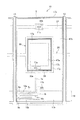
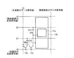
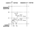
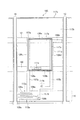
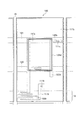
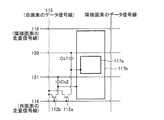
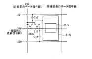
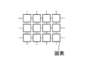
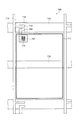
12a・12b TFT
15 データ信号線
16 走査信号線
17a 第1の副画素電極
17b 第2の副画素電極
11a・11b コンタクトホール
20 第1の保持容量配線
21 第2の保持容量配線
Claims (5)
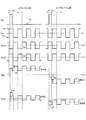
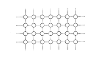
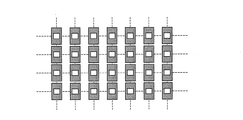
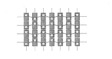
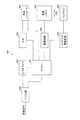
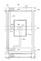
- 画素に中間調を表示する時に、該画素内の第1および第2副画素電極を異なる実効電位とすることで第1副画素電極に対応する第1輝度領域を第2副画素電極に対応する第2輝度領域よりも高輝度とする表示装置であって、
走査信号線と、データ信号線と、第1および第2保持容量配線と、第1保持容量配線に重なる第1保持容量上電極と、第2保持容量配線に重なる第2保持容量上電極とが設けられ、
第1および第2副画素電極はそれぞれ、上記走査信号線に接続するトランジスタを介して上記データ信号線に接続され、
第1保持容量上電極は第1副画素電極に接続されるとともに、第2保持容量上電極は第2副画素電極に接続され、
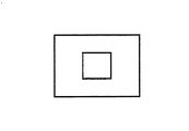
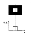
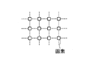
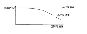
第2副画素電極は平面的に視て内周および外周を有する形状であって、かつ第2副画素電極の内周の内側に第1副画素電極が配されていることにより、中間調を表示する時に第2輝度領域が第1輝度領域を取り囲み、上記第1および第2輝度領域の間隙には最低輝度領域が形成され、
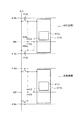
上記第1および第2保持容量配線は、第1副画素電極と重ならないように配されていることを特徴とする表示装置。 - 上記間隙と重なるように上記走査信号線が形成されていることを特徴とする請求項1記載の表示装置。
- 上記走査信号線が画素中段において額縁状に引き回されていることを特徴とする請求項2に記載の表示装置。
- 請求項1〜3のいずれか1項に記載の表示装置を備えることを特徴とする液晶表示装置。
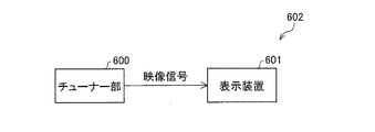
- 請求項4に記載の液晶表示装置と、テレビジョン放送を受信するチューナ部とを備えることを特徴とするテレビジョン受像機。
Priority Applications (1)
| Application Number | Priority Date | Filing Date | Title |
|---|---|---|---|
| JP2010023578A JP5073766B2 (ja) | 2006-02-06 | 2010-02-04 | 表示装置、液晶表示装置、テレビジョン受像機 |
Applications Claiming Priority (5)
| Application Number | Priority Date | Filing Date | Title |
|---|---|---|---|
| JP2006029043 | 2006-02-06 | ||
| JP2006029043 | 2006-02-06 | ||
| JP2006248558 | 2006-09-13 | ||
| JP2006248558 | 2006-09-13 | ||
| JP2010023578A JP5073766B2 (ja) | 2006-02-06 | 2010-02-04 | 表示装置、液晶表示装置、テレビジョン受像機 |
Related Parent Applications (1)
| Application Number | Title | Priority Date | Filing Date |
|---|---|---|---|
| JP2007557747A Division JPWO2007091365A1 (ja) | 2006-02-06 | 2006-11-30 | 表示装置、アクティブマトリクス基板、液晶表示装置、テレビジョン受像機 |
Publications (3)
| Publication Number | Publication Date |
|---|---|
| JP2010160493A JP2010160493A (ja) | 2010-07-22 |
| JP2010160493A5 JP2010160493A5 (ja) | 2010-09-02 |
| JP5073766B2 true JP5073766B2 (ja) | 2012-11-14 |
Family
ID=38344972
Family Applications (2)
| Application Number | Title | Priority Date | Filing Date |
|---|---|---|---|
| JP2007557747A Pending JPWO2007091365A1 (ja) | 2006-02-06 | 2006-11-30 | 表示装置、アクティブマトリクス基板、液晶表示装置、テレビジョン受像機 |
| JP2010023578A Expired - Fee Related JP5073766B2 (ja) | 2006-02-06 | 2010-02-04 | 表示装置、液晶表示装置、テレビジョン受像機 |
Family Applications Before (1)
| Application Number | Title | Priority Date | Filing Date |
|---|---|---|---|
| JP2007557747A Pending JPWO2007091365A1 (ja) | 2006-02-06 | 2006-11-30 | 表示装置、アクティブマトリクス基板、液晶表示装置、テレビジョン受像機 |
Country Status (3)
| Country | Link |
|---|---|
| US (1) | US20090009449A1 (ja) |
| JP (2) | JPWO2007091365A1 (ja) |
| WO (1) | WO2007091365A1 (ja) |
Families Citing this family (36)
| Publication number | Priority date | Publication date | Assignee | Title |
|---|---|---|---|---|
| KR101244332B1 (ko) * | 2006-09-18 | 2013-03-18 | 삼성디스플레이 주식회사 | 표시장치 |
| TWI360010B (en) * | 2007-09-20 | 2012-03-11 | Chimei Innolux Corp | Pixel array substrate and liquid crystal display |
| KR101508639B1 (ko) | 2007-11-29 | 2015-04-06 | 가부시키가이샤 한도오따이 에네루기 켄큐쇼 | 액정 표시장치 및 전자기기 |
| KR101448001B1 (ko) * | 2008-01-29 | 2014-10-13 | 삼성디스플레이 주식회사 | 액정 표시 장치 |
| KR20090103461A (ko) | 2008-03-28 | 2009-10-01 | 삼성전자주식회사 | 액정 표시 장치 |
| JP4626664B2 (ja) * | 2008-03-31 | 2011-02-09 | カシオ計算機株式会社 | 液晶表示装置 |
| TWI377383B (en) * | 2008-05-05 | 2012-11-21 | Au Optronics Corp | Pixel, display and the driving method thereof |
| JP5305755B2 (ja) * | 2008-06-27 | 2013-10-02 | 三菱電機株式会社 | 液晶表示装置 |
| KR101540302B1 (ko) * | 2008-07-09 | 2015-07-29 | 삼성디스플레이 주식회사 | 표시기판 및 이를 갖는 액정표시패널 |
| JP4706729B2 (ja) | 2008-07-14 | 2011-06-22 | カシオ計算機株式会社 | 液晶表示装置 |
| KR101518327B1 (ko) * | 2008-07-24 | 2015-05-11 | 삼성디스플레이 주식회사 | 액정 표시판 및 액정 표시 장치 |
| KR101595817B1 (ko) | 2008-08-22 | 2016-02-22 | 삼성디스플레이 주식회사 | 액정 표시 장치 |
| KR101549962B1 (ko) * | 2008-11-28 | 2015-09-04 | 삼성디스플레이 주식회사 | 액정 표시 장치 |
| EP2357520A4 (en) | 2008-12-10 | 2012-05-30 | Sharp Kk | ACTIVE MATRIX SUBSTRATE, PROCESS FOR PREPARING AN ACTIVE MATRIX SUBSTRATE, LIQUID CRYSTAL SCREEN, METHOD FOR PRODUCING A LIQUID CRYSTAL SCREEN, LIQUID CRYSTAL DISPLAY ARRANGEMENT, LIQUID CRYSTAL DISPLAY UNIT AND TV RECEIVER |
| JP5348473B2 (ja) * | 2009-01-20 | 2013-11-20 | ソニー株式会社 | 液晶表示装置および電子機器 |
| WO2010146756A1 (ja) | 2009-06-17 | 2010-12-23 | シャープ株式会社 | フリップフロップ、シフトレジスタ、表示駆動回路、表示装置、表示パネル |
| TWI420212B (zh) * | 2009-12-31 | 2013-12-21 | Au Optronics Corp | 畫素陣列 |
| WO2011099217A1 (ja) * | 2010-02-15 | 2011-08-18 | シャープ株式会社 | アクティブマトリクス基板、液晶パネル、液晶表示装置、テレビジョン受像機 |
| JP5418390B2 (ja) * | 2010-04-27 | 2014-02-19 | カシオ計算機株式会社 | 液晶表示装置 |
| JP5538559B2 (ja) * | 2010-11-02 | 2014-07-02 | シャープ株式会社 | 表示装置 |
| US9190001B2 (en) | 2010-11-09 | 2015-11-17 | Sharp Kabushiki Kaisha | Liquid crystal display device, display apparatus, and gate signal line driving method |
| KR101813517B1 (ko) * | 2011-04-06 | 2018-01-02 | 삼성디스플레이 주식회사 | 표시 패널의 구동 방법 및 이를 수행하는 표시 장치 |
| TWI446079B (zh) * | 2011-06-29 | 2014-07-21 | Au Optronics Corp | 畫素結構及其驅動方法 |
| WO2013069559A1 (ja) * | 2011-11-10 | 2013-05-16 | シャープ株式会社 | 表示装置およびその駆動方法 |
| KR101948694B1 (ko) | 2012-02-09 | 2019-02-18 | 삼성디스플레이 주식회사 | 액정 표시 장치 |
| KR101944701B1 (ko) * | 2012-09-05 | 2019-02-11 | 삼성디스플레이 주식회사 | 표시 패널 및 이의 제조 방법 |
| CN103854614B (zh) * | 2014-02-24 | 2016-06-29 | 北京京东方显示技术有限公司 | 背光控制电路和液晶显示装置 |
| KR20150114638A (ko) * | 2014-04-01 | 2015-10-13 | 삼성디스플레이 주식회사 | 액정 표시 장치 |
| KR101635954B1 (ko) * | 2014-12-31 | 2016-07-07 | 삼성디스플레이 주식회사 | 액정 표시 장치 |
| KR20160087022A (ko) * | 2015-01-12 | 2016-07-21 | 삼성디스플레이 주식회사 | 표시패널 |
| KR101681487B1 (ko) * | 2015-07-16 | 2016-12-02 | 삼성디스플레이 주식회사 | 액정 표시 장치 |
| EP3537209B1 (en) * | 2017-01-10 | 2021-09-15 | BOE Technology Group Co., Ltd. | Array substrate comprising a subpixel unit, control method therefor, and display device |
| TWI648720B (zh) * | 2017-10-25 | 2019-01-21 | 元太科技工業股份有限公司 | 顯示裝置 |
| CN108389557B (zh) * | 2018-03-16 | 2020-01-21 | 京东方科技集团股份有限公司 | 显示装置及其驱动方法 |
| CN112349749B (zh) * | 2019-12-30 | 2022-08-05 | 广东聚华印刷显示技术有限公司 | 像素排列结构、发光器件及显示面板 |
| TWI724795B (zh) * | 2020-02-18 | 2021-04-11 | 友達光電股份有限公司 | 畫素結構 |
Family Cites Families (26)
| Publication number | Priority date | Publication date | Assignee | Title |
|---|---|---|---|---|
| GB8622715D0 (en) * | 1986-09-20 | 1986-10-29 | Emi Plc Thorn | Display device |
| JP3081357B2 (ja) * | 1992-04-15 | 2000-08-28 | 富士通株式会社 | 液晶表示装置及びその製造方法 |
| KR100295712B1 (ko) * | 1994-03-11 | 2001-11-14 | 미다라이 후지오 | 컴퓨터디스플레이시스템컨트롤러 |
| EP0673011B1 (en) * | 1994-03-11 | 1999-06-02 | Canon Kabushiki Kaisha | Dynamic refinement of pixel structure in a display |
| AUPM440994A0 (en) * | 1994-03-11 | 1994-04-14 | Canon Information Systems Research Australia Pty Ltd | A luminance weighted discrete level display |
| KR100259783B1 (ko) * | 1994-03-11 | 2000-06-15 | 미다라이 후지오 | 다수의 컬러 개별 레벨 디스플레이를 위한 디스플레이 픽셀 밸런싱 |
| AUPM440494A0 (en) * | 1994-03-11 | 1994-04-14 | Canon Information Systems Research Australia Pty Ltd | Intermingling subpixels in discrete level displays |
| US5610739A (en) * | 1994-05-31 | 1997-03-11 | Matsushita Electric Industrial Co., Ltd. | Liquid crystal display unit with a plurality of subpixels |
| JP3164987B2 (ja) * | 1994-12-22 | 2001-05-14 | 松下電器産業株式会社 | アクティブマトリックス型液晶表示素子 |
| JP3662316B2 (ja) * | 1994-10-24 | 2005-06-22 | 株式会社半導体エネルギー研究所 | 液晶表示装置および液晶表示装置の駆動方法 |
| TW295652B (ja) * | 1994-10-24 | 1997-01-11 | Handotai Energy Kenkyusho Kk | |
| JPH08179341A (ja) * | 1994-12-22 | 1996-07-12 | Matsushita Electric Ind Co Ltd | 液晶表示装置およびその駆動方法 |
| JP3520382B2 (ja) * | 1995-02-01 | 2004-04-19 | セイコーエプソン株式会社 | 液晶表示装置 |
| JP2001222027A (ja) * | 2000-02-09 | 2001-08-17 | Seiko Epson Corp | 電気光学装置および投射型表示装置 |
| US6515728B1 (en) * | 2000-09-07 | 2003-02-04 | Lg.Philips Lcd Co., Ltd. | Multi-domain liquid crystal display device |
| CN1394320A (zh) * | 2000-10-27 | 2003-01-29 | 松下电器产业株式会社 | 显示器件 |
| JP2002333870A (ja) * | 2000-10-31 | 2002-11-22 | Matsushita Electric Ind Co Ltd | 液晶表示装置、el表示装置及びその駆動方法、並びに副画素の表示パターン評価方法 |
| JP2002328386A (ja) * | 2001-04-27 | 2002-11-15 | Sanyo Electric Co Ltd | アクティブマトリクス型表示装置 |
| US6956553B2 (en) * | 2001-04-27 | 2005-10-18 | Sanyo Electric Co., Ltd. | Active matrix display device |
| TWI271573B (en) * | 2001-08-22 | 2007-01-21 | Advanced Display Kk | Liquid crystal display device and method of producing the same |
| JP4342200B2 (ja) * | 2002-06-06 | 2009-10-14 | シャープ株式会社 | 液晶表示装置 |
| JP4248306B2 (ja) * | 2002-06-17 | 2009-04-02 | シャープ株式会社 | 液晶表示装置 |
| JP4467334B2 (ja) * | 2004-03-04 | 2010-05-26 | シャープ株式会社 | 液晶表示装置 |
| JP4394512B2 (ja) * | 2004-04-30 | 2010-01-06 | 富士通株式会社 | 視角特性を改善した液晶表示装置 |
| CN100523923C (zh) * | 2004-10-06 | 2009-08-05 | 夏普株式会社 | 液晶显示器 |
| JP4419944B2 (ja) * | 2005-03-29 | 2010-02-24 | セイコーエプソン株式会社 | 電気泳動表示装置及びその駆動方法 |
-
2006
- 2006-11-30 JP JP2007557747A patent/JPWO2007091365A1/ja active Pending
- 2006-11-30 WO PCT/JP2006/323966 patent/WO2007091365A1/ja not_active Ceased
- 2006-11-30 US US12/087,863 patent/US20090009449A1/en not_active Abandoned
-
2010
- 2010-02-04 JP JP2010023578A patent/JP5073766B2/ja not_active Expired - Fee Related
Also Published As
| Publication number | Publication date |
|---|---|
| JP2010160493A (ja) | 2010-07-22 |
| JPWO2007091365A1 (ja) | 2009-07-02 |
| WO2007091365A1 (ja) | 2007-08-16 |
| US20090009449A1 (en) | 2009-01-08 |
Similar Documents
| Publication | Publication Date | Title |
|---|---|---|
| JP5073766B2 (ja) | 表示装置、液晶表示装置、テレビジョン受像機 | |
| JP4932823B2 (ja) | アクティブマトリクス基板、表示装置及びテレビジョン受像機 | |
| KR101369587B1 (ko) | 액정 표시 장치 | |
| JP4938032B2 (ja) | 液晶パネル、液晶表示装置、およびテレビジョン装置 | |
| JP5214466B2 (ja) | 液晶表示パネル、液晶表示素子、及び、液晶表示装置 | |
| CN101960371B (zh) | 有源矩阵基板、液晶面板、液晶显示装置、液晶显示单元、以及电视接收机 | |
| US7907106B2 (en) | Liquid crystal display and driving method thereof | |
| JP5107421B2 (ja) | アクティブマトリクス基板、液晶パネル、液晶表示装置、液晶表示ユニット、テレビジョン受像機 | |
| JP4541421B2 (ja) | 液晶表示装置、テレビジョン受像機 | |
| JP5220863B2 (ja) | アクティブマトリクス基板、液晶パネル、液晶表示ユニット、液晶表示装置、テレビジョン受像機 | |
| JP2007086791A (ja) | 液晶パネル、その駆動方法、及びそれを用いた液晶表示装置 | |
| US6130654A (en) | Driving method of a liquid crystal display device | |
| JP5179670B2 (ja) | 液晶表示装置 | |
| WO2010089820A1 (ja) | アクティブマトリクス基板、液晶パネル、液晶表示ユニット、液晶表示装置、テレビジョン受像機 | |
| WO2010100788A1 (ja) | アクティブマトリクス基板、液晶パネル、液晶表示装置、液晶表示ユニット、テレビジョン受像機 | |
| KR102764289B1 (ko) | 이형 액정 표시 패널 | |
| CN101361109A (zh) | 显示装置、有源矩阵基板、液晶显示装置、电视接收机 | |
| US10741135B2 (en) | Liquid crystal display device | |
| JP5301567B2 (ja) | アクティブマトリクス基板、アクティブマトリクス基板の製造方法、液晶パネル、液晶パネルの製造方法、液晶表示装置、液晶表示ユニット、テレビジョン受像機 | |
| JP2004240263A (ja) | 表示駆動装置及びその駆動制御方法 | |
| WO2013008771A1 (ja) | 液晶表示装置、液晶表示装置の駆動方法、およびパルス波形信号調整方法 | |
| JP2004294913A (ja) | 液晶表示装置 |
Legal Events
| Date | Code | Title | Description |
|---|---|---|---|
| A521 | Written amendment |
Free format text: JAPANESE INTERMEDIATE CODE: A523 Effective date: 20100712 |
|
| A131 | Notification of reasons for refusal |
Free format text: JAPANESE INTERMEDIATE CODE: A131 Effective date: 20120515 |
|
| A521 | Written amendment |
Free format text: JAPANESE INTERMEDIATE CODE: A523 Effective date: 20120711 |
|
| TRDD | Decision of grant or rejection written | ||
| A01 | Written decision to grant a patent or to grant a registration (utility model) |
Free format text: JAPANESE INTERMEDIATE CODE: A01 Effective date: 20120821 |
|
| A01 | Written decision to grant a patent or to grant a registration (utility model) |
Free format text: JAPANESE INTERMEDIATE CODE: A01 |
|
| A61 | First payment of annual fees (during grant procedure) |
Free format text: JAPANESE INTERMEDIATE CODE: A61 Effective date: 20120822 |
|
| R150 | Certificate of patent or registration of utility model |
Ref document number: 5073766 Country of ref document: JP Free format text: JAPANESE INTERMEDIATE CODE: R150 Free format text: JAPANESE INTERMEDIATE CODE: R150 |
|
| FPAY | Renewal fee payment (event date is renewal date of database) |
Free format text: PAYMENT UNTIL: 20150831 Year of fee payment: 3 |
|
| LAPS | Cancellation because of no payment of annual fees |