JP5073766B2 - Display device, liquid crystal display device, television receiver - Google Patents
Display device, liquid crystal display device, television receiver Download PDFInfo
- Publication number
- JP5073766B2 JP5073766B2 JP2010023578A JP2010023578A JP5073766B2 JP 5073766 B2 JP5073766 B2 JP 5073766B2 JP 2010023578 A JP2010023578 A JP 2010023578A JP 2010023578 A JP2010023578 A JP 2010023578A JP 5073766 B2 JP5073766 B2 JP 5073766B2
- Authority
- JP
- Japan
- Prior art keywords
- storage capacitor
- electrode
- display device
- subpixel electrode
- subpixel
- Prior art date
- Legal status (The legal status is an assumption and is not a legal conclusion. Google has not performed a legal analysis and makes no representation as to the accuracy of the status listed.)
- Expired - Fee Related
Links
Images

Classifications
-
- G—PHYSICS
- G02—OPTICS
- G02F—OPTICAL DEVICES OR ARRANGEMENTS FOR THE CONTROL OF LIGHT BY MODIFICATION OF THE OPTICAL PROPERTIES OF THE MEDIA OF THE ELEMENTS INVOLVED THEREIN; NON-LINEAR OPTICS; FREQUENCY-CHANGING OF LIGHT; OPTICAL LOGIC ELEMENTS; OPTICAL ANALOGUE/DIGITAL CONVERTERS
- G02F1/00—Devices or arrangements for the control of the intensity, colour, phase, polarisation or direction of light arriving from an independent light source, e.g. switching, gating or modulating; Non-linear optics
- G02F1/01—Devices or arrangements for the control of the intensity, colour, phase, polarisation or direction of light arriving from an independent light source, e.g. switching, gating or modulating; Non-linear optics for the control of the intensity, phase, polarisation or colour
- G02F1/13—Devices or arrangements for the control of the intensity, colour, phase, polarisation or direction of light arriving from an independent light source, e.g. switching, gating or modulating; Non-linear optics for the control of the intensity, phase, polarisation or colour based on liquid crystals, e.g. single liquid crystal display cells
- G02F1/133—Constructional arrangements; Operation of liquid crystal cells; Circuit arrangements
- G02F1/136—Liquid crystal cells structurally associated with a semi-conducting layer or substrate, e.g. cells forming part of an integrated circuit
- G02F1/1362—Active matrix addressed cells
- G02F1/13624—Active matrix addressed cells having more than one switching element per pixel
-
- G—PHYSICS
- G09—EDUCATION; CRYPTOGRAPHY; DISPLAY; ADVERTISING; SEALS
- G09G—ARRANGEMENTS OR CIRCUITS FOR CONTROL OF INDICATING DEVICES USING STATIC MEANS TO PRESENT VARIABLE INFORMATION
- G09G3/00—Control arrangements or circuits, of interest only in connection with visual indicators other than cathode-ray tubes
- G09G3/20—Control arrangements or circuits, of interest only in connection with visual indicators other than cathode-ray tubes for presentation of an assembly of a number of characters, e.g. a page, by composing the assembly by combination of individual elements arranged in a matrix no fixed position being assigned to or needed to be assigned to the individual characters or partial characters
- G09G3/34—Control arrangements or circuits, of interest only in connection with visual indicators other than cathode-ray tubes for presentation of an assembly of a number of characters, e.g. a page, by composing the assembly by combination of individual elements arranged in a matrix no fixed position being assigned to or needed to be assigned to the individual characters or partial characters by control of light from an independent source
- G09G3/36—Control arrangements or circuits, of interest only in connection with visual indicators other than cathode-ray tubes for presentation of an assembly of a number of characters, e.g. a page, by composing the assembly by combination of individual elements arranged in a matrix no fixed position being assigned to or needed to be assigned to the individual characters or partial characters by control of light from an independent source using liquid crystals
- G09G3/3611—Control of matrices with row and column drivers
- G09G3/3648—Control of matrices with row and column drivers using an active matrix
-
- G—PHYSICS
- G02—OPTICS
- G02F—OPTICAL DEVICES OR ARRANGEMENTS FOR THE CONTROL OF LIGHT BY MODIFICATION OF THE OPTICAL PROPERTIES OF THE MEDIA OF THE ELEMENTS INVOLVED THEREIN; NON-LINEAR OPTICS; FREQUENCY-CHANGING OF LIGHT; OPTICAL LOGIC ELEMENTS; OPTICAL ANALOGUE/DIGITAL CONVERTERS
- G02F1/00—Devices or arrangements for the control of the intensity, colour, phase, polarisation or direction of light arriving from an independent light source, e.g. switching, gating or modulating; Non-linear optics
- G02F1/01—Devices or arrangements for the control of the intensity, colour, phase, polarisation or direction of light arriving from an independent light source, e.g. switching, gating or modulating; Non-linear optics for the control of the intensity, phase, polarisation or colour
- G02F1/13—Devices or arrangements for the control of the intensity, colour, phase, polarisation or direction of light arriving from an independent light source, e.g. switching, gating or modulating; Non-linear optics for the control of the intensity, phase, polarisation or colour based on liquid crystals, e.g. single liquid crystal display cells
- G02F1/133—Constructional arrangements; Operation of liquid crystal cells; Circuit arrangements
- G02F1/1333—Constructional arrangements; Manufacturing methods
- G02F1/1343—Electrodes
- G02F1/134309—Electrodes characterised by their geometrical arrangement
- G02F1/134345—Subdivided pixels, e.g. for grey scale or redundancy
-
- G—PHYSICS
- G09—EDUCATION; CRYPTOGRAPHY; DISPLAY; ADVERTISING; SEALS
- G09G—ARRANGEMENTS OR CIRCUITS FOR CONTROL OF INDICATING DEVICES USING STATIC MEANS TO PRESENT VARIABLE INFORMATION
- G09G2300/00—Aspects of the constitution of display devices
- G09G2300/04—Structural and physical details of display devices
- G09G2300/0421—Structural details of the set of electrodes
- G09G2300/0426—Layout of electrodes and connections
-
- G—PHYSICS
- G09—EDUCATION; CRYPTOGRAPHY; DISPLAY; ADVERTISING; SEALS
- G09G—ARRANGEMENTS OR CIRCUITS FOR CONTROL OF INDICATING DEVICES USING STATIC MEANS TO PRESENT VARIABLE INFORMATION
- G09G2300/00—Aspects of the constitution of display devices
- G09G2300/04—Structural and physical details of display devices
- G09G2300/0439—Pixel structures
- G09G2300/0443—Pixel structures with several sub-pixels for the same colour in a pixel, not specifically used to display gradations
- G09G2300/0447—Pixel structures with several sub-pixels for the same colour in a pixel, not specifically used to display gradations for multi-domain technique to improve the viewing angle in a liquid crystal display, such as multi-vertical alignment [MVA]
-
- G—PHYSICS
- G09—EDUCATION; CRYPTOGRAPHY; DISPLAY; ADVERTISING; SEALS
- G09G—ARRANGEMENTS OR CIRCUITS FOR CONTROL OF INDICATING DEVICES USING STATIC MEANS TO PRESENT VARIABLE INFORMATION
- G09G2300/00—Aspects of the constitution of display devices
- G09G2300/08—Active matrix structure, i.e. with use of active elements, inclusive of non-linear two terminal elements, in the pixels together with light emitting or modulating elements
- G09G2300/0876—Supplementary capacities in pixels having special driving circuits and electrodes instead of being connected to common electrode or ground; Use of additional capacitively coupled compensation electrodes
-
- G—PHYSICS
- G09—EDUCATION; CRYPTOGRAPHY; DISPLAY; ADVERTISING; SEALS
- G09G—ARRANGEMENTS OR CIRCUITS FOR CONTROL OF INDICATING DEVICES USING STATIC MEANS TO PRESENT VARIABLE INFORMATION
- G09G2310/00—Command of the display device
- G09G2310/02—Addressing, scanning or driving the display screen or processing steps related thereto
- G09G2310/0235—Field-sequential colour display
-
- G—PHYSICS
- G09—EDUCATION; CRYPTOGRAPHY; DISPLAY; ADVERTISING; SEALS
- G09G—ARRANGEMENTS OR CIRCUITS FOR CONTROL OF INDICATING DEVICES USING STATIC MEANS TO PRESENT VARIABLE INFORMATION
- G09G2320/00—Control of display operating conditions
- G09G2320/02—Improving the quality of display appearance
- G09G2320/028—Improving the quality of display appearance by changing the viewing angle properties, e.g. widening the viewing angle, adapting the viewing angle to the view direction
Landscapes
- Physics & Mathematics (AREA)
- Engineering & Computer Science (AREA)
- Nonlinear Science (AREA)
- General Physics & Mathematics (AREA)
- Chemical & Material Sciences (AREA)
- Crystallography & Structural Chemistry (AREA)
- Mathematical Physics (AREA)
- Microelectronics & Electronic Packaging (AREA)
- Optics & Photonics (AREA)
- Computer Hardware Design (AREA)
- Theoretical Computer Science (AREA)
- Liquid Crystal (AREA)
- Liquid Crystal Display Device Control (AREA)
- Control Of Indicators Other Than Cathode Ray Tubes (AREA)
- Devices For Indicating Variable Information By Combining Individual Elements (AREA)
Description
本発明は、液晶表示装置およびそれに用いられるアクティブマトリクス基板に関する。 The present invention relates to a liquid crystal display device and an active matrix substrate used therefor.
図36は、液晶表示装置に用いられる従来のアクティブマトリクス基板の構成である。同図に示されるように、アクティブマトリクス基板700には、交差配置された複数の走査信号線716および複数のデータ信号線715と、各信号線(715・716)の交点近傍に形成されたTFT712(Thin Film Transistor:薄膜トランジスタ)と、画素電極717とを備える。走査信号線716はTFT712のゲート電極を兼ねており、TFT712のソース電極719がデータ信号線715に接続され、ドレイン電極708がドレイン引き出し電極707を介して画素電極717に接続される。ドレイン引き出し電極と画素電極717との間に配される絶縁膜には穴が開けられており、これによってドレイン引き出し電極707と画素電極717とを接続するコンタクトホール710が形成されている。画素電極717はITO等の透明電極であり、アクティブマトリクス基板下からの光(バックライト光)を透過させる。
FIG. 36 shows a configuration of a conventional active matrix substrate used in a liquid crystal display device. As shown in the figure, the
このアクティブマトリクス基板700においては、走査信号線716に送られる走査信号(ゲートON電圧)によってTFT712がON(ソース電極719とドレイン電極708とが導通状態)状態となり、この状態においてデータ信号線715に送られるデータ信号(信号電圧)が、ソース電極719、ドレイン電極708およびドレイン引き出し電極707を介して画素電極717に書き込まれる。なお、保持容量(Cs)配線718は、TFT712のオフ期間中における液晶層の自己放電を回避する等の機能を有する。
In this
ここで、アクティブマトリクス基板700においては、各画素内の画素電極717全体が等電位となる。すなわち、アクティブマトリクス基板700を液晶表示装置に用いた場合には、全体がほぼ均一輝度の画素によって表示が行われることになる。
Here, in the
なお、特許文献1には、γ特性の視野角依存性を抑制するため、各画素を上下2つの副画素に分割し、一方の副画素を高輝度の明画素とし、もう一方の副画素を低輝度の暗画素とする構成が開示されている。 In Patent Document 1, in order to suppress the viewing angle dependency of the γ characteristic, each pixel is divided into two upper and lower subpixels, one subpixel is a bright pixel with high luminance, and the other subpixel is A configuration in which a low-luminance dark pixel is used is disclosed.
しかしながら、各画素内の輝度を均一にして表示を行うと、図21(b)に示されるような空間周波数の高い映像がぼやけてしまうという問題がある。また、特許文献1に開示された、上下に配した副画素間で輝度を異ならせる構成でも、空間周波数の高い映像の表示ぼけを十分に改善することができていない。 However, if the display is performed with the luminance in each pixel uniform, there is a problem that an image with a high spatial frequency as shown in FIG. In addition, even in the configuration disclosed in Patent Document 1 in which the luminance is different between the subpixels arranged above and below, display blur of an image having a high spatial frequency cannot be sufficiently improved.
本発明は、上記課題に鑑みてなされたものであり、その目的は、空間周波数の高い映像を鮮明に表示できる表示装置およびそれに用いるアクティブマトリクス基板を提供する点にある。 The present invention has been made in view of the above problems, and an object thereof is to provide a display device capable of clearly displaying an image having a high spatial frequency and an active matrix substrate used therefor.
本発明の表示装置は、複数の画素を備え、各画素内に、第1の輝度領域(高輝度領域)と、該第1の輝度領域を取り囲むとともに第1の輝度領域より輝度の低い第2の輝度領域(低輝度領域)とを形成できることを特徴とする。すなわち、本表示装置は、各画素に、周囲より高輝度に制御可能な第1の輝度領域と、該第1の輝度領域を取り囲むとともに該第1の輝度領域より低輝度に制御可能な第2の輝度領域とを備えている。 The display device of the present invention includes a plurality of pixels, and each pixel includes a first luminance region (high luminance region), a second luminance that surrounds the first luminance region and has a lower luminance than the first luminance region. Luminance region (low luminance region) can be formed. That is, the display device includes, in each pixel, a first luminance region that can be controlled to have higher luminance than the surroundings, and a second luminance that surrounds the first luminance region and can be controlled to have lower luminance than the first luminance region. Brightness area.
例えば3原色(R・G・B)の同時加法混色方式の表示装置であれば、3原色それぞれに対応して1つの画素が設けられる。この場合、3原色に対する3つの画素がストライプ状、モザイク状あるいはデルタ状等に配される。 For example, in the case of a display device using a simultaneous additive color mixing method of three primary colors (R, G, and B), one pixel is provided for each of the three primary colors. In this case, three pixels for the three primary colors are arranged in a stripe shape, a mosaic shape, a delta shape, or the like.
このように、本表示装置は、各画素に、高輝度領域とこれを取り囲む低輝度領域とを形成できるように構成されているため、画素全体の輝度総和の全部あるいは大半を高輝度領域で賄って(光放射を画素中央に集中させて)中間調表示を行うことができる。これにより、高空間周波数領域における伝達特性が向上し、空間周波数の高い映像を鮮明に表示することができる。 As described above, the display device is configured so that a high luminance region and a low luminance region surrounding the high luminance region can be formed in each pixel. Therefore, the high luminance region covers all or most of the total luminance of the entire pixel. (Concentrating the light emission at the center of the pixel) enables halftone display. Thereby, transfer characteristics in a high spatial frequency region are improved, and an image with a high spatial frequency can be clearly displayed.
本表示装置においては、各画素は、第1および第2のスイッチング素子と、該第1のスイッチング素子に接続する第1の副画素電極と、上記第2のスイッチング素子に接続し、第1の副画素電極を取り囲む第2の副画素電極と、を備えている構成とすることもできる。 In the display device, each pixel is connected to the first and second switching elements, the first subpixel electrode connected to the first switching element, the second switching element, and the first switching element. A second subpixel electrode surrounding the subpixel electrode may be provided.
本表示装置においては、上記第1および第2の輝度領域は、ともに同一点を重心とする形状であることが好ましい。この構成によれば、映像信号に対応する位置情報を正確に再現でき、ギザギザ感のない自然な映像表現が可能となる。 In the present display device, it is preferable that the first and second luminance regions have a shape having the same point as the center of gravity. According to this configuration, position information corresponding to the video signal can be accurately reproduced, and natural video expression without jaggedness can be achieved.
本表示装置においては、上記第1の輝度領域(高輝度領域)と第2の輝度領域(低輝度領域)との間に最低輝度領域が形成されることが好ましい。このように最低輝度領域を形成する(例えば高輝度領域の外周を遮光する)ことで、光漏れによるコントラスト低下を防止することができる。なお、上記のように最低輝度領域を設けることなく、第1の輝度領域(高輝度領域)と第2の輝度領域(低輝度領域)とを隣接させることも可能である。 In this display device, it is preferable that a minimum luminance region is formed between the first luminance region (high luminance region) and the second luminance region (low luminance region). By forming the lowest luminance region in this way (for example, shielding the outer periphery of the high luminance region), it is possible to prevent a decrease in contrast due to light leakage. Note that the first luminance region (high luminance region) and the second luminance region (low luminance region) can be adjacent to each other without providing the lowest luminance region as described above.
アクティブマトリクス基板とカラーフィルタ基板とを備えた本表示装置においては、上記最低輝度領域が、カラーフィルタ基板に設けられたブラックマトリクス、およびアクティブマトリクス基板に設けられた遮光体の少なくとも一方によって形成されていてもよい。こうすれば、(高輝度領域外周近傍からの)光漏れ防止用部材を別途設ける必要がないため製造工程が簡略化でき製造コストを抑えることができる。 In the present display device including the active matrix substrate and the color filter substrate, the minimum luminance region is formed by at least one of a black matrix provided on the color filter substrate and a light shielding member provided on the active matrix substrate. May be. In this case, it is not necessary to separately provide a light leakage prevention member (from the vicinity of the outer periphery of the high luminance region), so that the manufacturing process can be simplified and the manufacturing cost can be reduced.
本表示装置においては、第1および第2のスイッチング素子が同一のデータ信号線に接続する構成とすることもできる。また、第1および第2のスイッチング素子は同一の走査信号線に接続している構成とすることもできる。この場合、例えば、上記第1の副画素電極と容量を形成する第1の保持容量配線と、上記第2の副画素電極と容量を形成する第2の保持容量配線とを設け、さらに、この第1および第2の保持容量配線の電位それぞれを個別に制御できるようにする。具体的には、各保持容量配線に互いに逆位相の信号電圧を印加する。こうすれば、第1および第2の各副画素電極の実効電圧を容易に制御することができ、高輝度領域および低輝度領域を容易に形成できる。この構成においては、上記第1および第2の保持容量配線を、それぞれの電位波形の位相が互いに180度ずれるように電位制御してもよい。また、上記第1および第2の保持容量配線それぞれを、第1および第2のスイッチング素子がオフされた後に電位が上昇あるいは降下するとともに、その状態が次フレームでこれらスイッチング素子がオフされるまで続くように電位制御してもよい。 In this display device, the first and second switching elements may be connected to the same data signal line. Further, the first and second switching elements may be connected to the same scanning signal line. In this case, for example, a first storage capacitor wiring that forms a capacity with the first subpixel electrode and a second storage capacity wiring that forms a capacity with the second subpixel electrode are provided. Each of the potentials of the first and second storage capacitor lines can be individually controlled. Specifically, signal voltages having opposite phases to each other are applied to the storage capacitor wires. In this way, the effective voltage of each of the first and second subpixel electrodes can be easily controlled, and a high luminance region and a low luminance region can be easily formed. In this configuration, the potentials of the first and second storage capacitor lines may be controlled so that the phases of the potential waveforms are shifted from each other by 180 degrees. In addition, the potential of the first and second storage capacitor lines is increased or decreased after the first and second switching elements are turned off until the switching elements are turned off in the next frame. The potential may be controlled to continue.
すなわち、上記第1の保持容量配線が、上記各スイッチング素子がオフされた後に電位が上昇してその状態が次フレームで上記各スイッチング素子がオフされるまで続くように電位制御されるとともに、上記第2の保持容量配線が、上記各スイッチング素子がオフされた後に電位が下降してその状態が次フレームで上記各スイッチング素子がオフされるまで続くように電位制御されるか、あるいは、上記第1の保持容量配線が、上記各スイッチング素子がオフされた後に電位が下降してその状態が次フレームで上記各スイッチング素子がオフされるまで続くように電位制御されるとともに、上記第2の保持容量配線が、上記各スイッチング素子がオフされた後に電位が上昇してその状態が次フレームで上記各スイッチング素子がオフされるまで続くように電位制御される。この場合、上記第1の保持容量配線の電位が上昇するのと第2の保持容量配線の電位が下降するのとが同期しているか、あるいは、上記第1の保持容量配線の電位が下降するのと第2の保持容量配線の電位が上昇するのとが同期している構成とすることができる。また、上記第1の保持容量配線の電位が上昇するのと第2の保持容量配線の電位が下降するのとが一水平期間ずれているか、あるいは、上記第1の保持容量配線の電位が下降するのと第2の保持容量配線の電位が上昇するのとが一水平期間ずれている構成とすることもできる。 That is, the potential of the first storage capacitor wiring is controlled so that the potential rises after the switching elements are turned off and the state continues until the switching elements are turned off in the next frame. The potential of the second storage capacitor wiring is controlled so that the potential drops after each of the switching elements is turned off and the state continues until the switching elements are turned off in the next frame, or The potential of the one storage capacitor wiring is controlled so that the potential drops after each of the switching elements is turned off and the state continues until the switching elements are turned off in the next frame, and the second holding The potential of the capacitor wiring rises after each switching element is turned off until the switching element is turned off in the next frame. It is as following potential control. In this case, the increase in the potential of the first storage capacitor line is synchronized with the decrease in the potential of the second storage capacitor line, or the potential of the first storage capacitor line decreases. And the potential of the second storage capacitor wiring is increased. Also, whether the potential of the first storage capacitor line increases and the potential of the second storage capacitor line decreases by one horizontal period, or the potential of the first storage capacitor line decreases. It is also possible to adopt a configuration in which the increase in the potential of the second storage capacitor wiring is shifted by one horizontal period.
本表示装置においては、第1および第2のスイッチング素子はそれぞれ、第1および第2の走査信号線に接続している構成とすることもできる。この場合、第1の走査信号線に供給されるオンパルスと第2の走査信号線に供給されるオンパルスとが時間的に重ならないようにすることもできるし、また、第1の走査信号線に供給されるオンパルスと第2の走査信号線に供給されるオンパルスとが、時間的に重なる部分を有しつつパルス終端をとるタイミングが異なるようにすることもできる。 In the present display device, the first and second switching elements may be connected to the first and second scanning signal lines, respectively. In this case, the on-pulse supplied to the first scanning signal line and the on-pulse supplied to the second scanning signal line can be prevented from overlapping with each other in time. The supplied on-pulse and the on-pulse supplied to the second scanning signal line may have different timings at the end of the pulse while having a temporally overlapping portion.
例えば、第1の走査信号線に供給されるオンパルスと第2の走査信号線に供給されるオンパルスとが、パルス始端をとるタイミングが同期し、パルス終端をとるタイミングは第1の走査信号線に供給されるオンパルスが先であるようにする。また、上記データ信号線に供給される電位は、一方のオンパルスが先にパルス終端をとるのと同期して、あるいはそれ以後に変化するようにする。こうすれば、第2の走査信号線が制御する第2のスイッチング素子に接続する第2の副画素電極には、ある電位が一旦与えられた状態で再度書き込むべき電位が与えられることになり、第2の副画素電極の充電を良好に行うことができる。特に、ドット反転駆動やHライン反転駆動のように水平期間ごとにデータ信号線に与えられる信号電位の極性が反転する(信号電位の波形が鈍ってしまう)場合や第2の副画素電極の面積が大きい(充電に時間がかかる)場合により効果的である。さらに、オンパルスの周期が長くなるため、走査信号の駆動周波数を抑制できるという効果もある。 For example, the on-pulse supplied to the first scanning signal line and the on-pulse supplied to the second scanning signal line are synchronized with each other at the timing at which the pulse start end is obtained, and the timing at which the pulse end is obtained is applied to the first scanning signal line. The on-pulse supplied is first. Further, the potential supplied to the data signal line is changed in synchronism with or after the end of one of the ON pulses. In this case, the second subpixel electrode connected to the second switching element controlled by the second scanning signal line is given a potential to be rewritten in a state where a certain potential is once given. The second subpixel electrode can be charged satisfactorily. In particular, when the polarity of the signal potential applied to the data signal line is inverted every horizontal period as in the case of dot inversion driving or H line inversion driving (the waveform of the signal potential becomes dull), or the area of the second subpixel electrode It is more effective when is large (it takes time to charge). Furthermore, since the cycle of the on-pulse becomes longer, there is an effect that the drive frequency of the scanning signal can be suppressed.
なお、上記構成においては、同一のデータ信号線に供給される電位の極性が、一水平期間ごとに反転させてもよい。 Note that in the above structure, the polarity of the potential supplied to the same data signal line may be inverted every horizontal period.
本表示装置においては、第1および第2のスイッチング素子がそれぞれ、互いに独立した第1および第2のデータ信号線に接続する構成とすることもできる。この場合には、第1および第2のデータ信号線に異なる信号電位を供給することによって上記第1の輝度領域および第2の輝度領域を形成する。 In this display device, the first and second switching elements may be connected to the first and second data signal lines that are independent of each other. In this case, the first luminance region and the second luminance region are formed by supplying different signal potentials to the first and second data signal lines.
本アクティブマトリクス基板は、複数の画素領域を備え、各画素領域に、第1および第2のスイッチング素子と、該第1のスイッチング素子に接続する第1の副画素電極と、上記第2のスイッチング素子に接続し、第1の副画素電極を取り囲む第2の副画素電極と、が設けられていることを特徴とする。 The active matrix substrate includes a plurality of pixel regions, and in each pixel region, first and second switching elements, a first subpixel electrode connected to the first switching element, and the second switching element. And a second subpixel electrode which is connected to the element and surrounds the first subpixel electrode.
本アクティブマトリクス基板は、これを表示装置に用いた場合に、各画素領域に対応する画素内に、高輝度領域とこれを取り囲む低輝度領域とを形成することが可能である。すなわち、画素全体の輝度総和の全部あるいはほとんどを画素中央の高輝度領域で賄って(光放射を画素中央に集中させて)中間調表示を行うことができる。このように、本アクティブマトリクス基板を備えた表示装置においては、高空間周波数領域における伝達特性が大幅に向上し、空間周波数の高い映像を鮮明に表示することが可能となる。 When this active matrix substrate is used in a display device, a high luminance region and a low luminance region surrounding the high luminance region can be formed in pixels corresponding to each pixel region. In other words, halftone display can be performed by covering all or most of the luminance sum of the entire pixel with the high luminance region at the center of the pixel (concentrating light emission at the center of the pixel). As described above, in the display device including the present active matrix substrate, the transfer characteristic in the high spatial frequency region is greatly improved, and an image with a high spatial frequency can be clearly displayed.
本アクティブマトリクス基板は、上記第1および第2のスイッチング素子が同一の走査信号線に接続されている構成とすることもできる。また、上記第1および第2のスイッチング素子が互いに独立した第1および第2の走査信号線に接続されている構成とすることもできる。 The present active matrix substrate may be configured such that the first and second switching elements are connected to the same scanning signal line. Further, the first and second switching elements may be connected to first and second scanning signal lines that are independent of each other.
本アクティブマトリクス基板は、各画素領域に1本のデータ信号線が配されるともに該データ信号線に上記第1および第2のスイッチング素子が接続され、かつ、上記第1の副画素電極と容量を形成する第1の保持容量配線と、上記第2の副画素電極と容量を形成する第2の保持容量配線とが設けられている構成とすることもできる。 In the active matrix substrate, one data signal line is arranged in each pixel region, the first and second switching elements are connected to the data signal line, and the first subpixel electrode and the capacitor are connected. A first storage capacitor wiring that forms a capacitor and a second storage capacitor wiring that forms a capacitor with the second subpixel electrode may be provided.
本アクティブマトリクス基板は、各画素領域に1本のデータ信号線が配されるともに該データ信号線に上記第1および第2のスイッチング素子が接続され、かつ、上記第1の副画素電極と容量を形成する第1の保持容量配線と、上記第2の副画素電極と容量を形成する第2の保持容量配線とが設けられている構成とすることもできる。 In the active matrix substrate, one data signal line is arranged in each pixel region, the first and second switching elements are connected to the data signal line, and the first subpixel electrode and the capacitor are connected. A first storage capacitor wiring that forms a capacitor and a second storage capacitor wiring that forms a capacitor with the second subpixel electrode may be provided.
本アクティブマトリクス基板は、各画素領域に互いに独立した第1および第2のデータ信号線が配され、この第1のデータ信号線に上記第1のスイッチング素子が接続されるとともに第2のデータ信号線に上記第2のスイッチング素子が接続されている構成とすることもできる。 In the present active matrix substrate, first and second data signal lines independent from each other are arranged in each pixel region, and the first switching element is connected to the first data signal line and a second data signal is connected. The second switching element may be connected to the line.
本アクティブマトリクス基板は、第1および第2の副画素電極の境界部分に重畳するように遮光体が形成されている構成とすることもできる。このように、第1および第2の副画素電極の境界部分を遮光することで、本アクティブマトリクス基板を備えた表示装置において、第1および第2の副画素電極の境界近傍(間隙領域)から光が漏れ、コントラストが低下するといった問題を回避することができる。また、アクティブマトリクス基板自体に遮光体を設けるため、カラーフィルタ基板に遮光体を設ける場合のように各基板を貼り合わせる際のずれによって遮光効果が低下してしまうといった問題も起こらない。なお、上記第1あるいは第2のスイッチング素子から引き出された配線の一部が、第1および第2の副画素電極の境界部分と重畳している構成とすることもできる。また、上記走査信号線の一部が、第1および第2の副画素電極の境界部分と重畳している構成とすることもできる。この場合、上記境界部分と重畳するように、上記走査信号線が画素中段において額縁状に引き回されていても良い。また、上記第1の保持容量配線の一部が、第1および第2の副画素電極の境界部分と重畳している構成とすることもできる。この場合、上記境界部分と重畳するように、上記第1の保持容量配線が画素中段において額縁状に引き回されていても良い。 The present active matrix substrate may be configured such that a light shielding body is formed so as to overlap with a boundary portion between the first and second subpixel electrodes. In this way, by shielding the boundary between the first and second subpixel electrodes, in the display device including the present active matrix substrate, from the vicinity of the boundary (gap region) between the first and second subpixel electrodes. Problems such as light leakage and a decrease in contrast can be avoided. In addition, since the active matrix substrate itself is provided with a light shielding body, there is no problem that the light shielding effect is reduced due to a shift in bonding the substrates as in the case of providing the light shielding body on the color filter substrate. Note that a part of the wiring extracted from the first or second switching element may overlap with the boundary portion between the first and second subpixel electrodes. In addition, a part of the scanning signal line may be overlapped with a boundary portion between the first and second subpixel electrodes. In this case, the scanning signal line may be drawn in a frame shape in the middle stage of the pixel so as to overlap with the boundary portion. Further, a part of the first storage capacitor wiring may overlap with a boundary portion between the first and second subpixel electrodes. In this case, the first storage capacitor line may be routed in a frame shape in the middle stage of the pixel so as to overlap with the boundary portion.
また、本発明の表示装置は、上記アクティブマトリクス基板を備えることを特徴とする。 In addition, a display device of the present invention includes the above active matrix substrate.
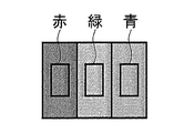
また、本発明の液晶表示装置は、上記アクティブマトリクス基板と、時分割で複数色を発するバックライトとを備え、フィールドシーケンシャル表示を行うことを特徴とする。この構成では、1つの画素に、例えば3原色(R・G・B)の3つの色が連続して表示される(もっとも、ある時刻には1つの画素に1つの色のみが表示される)。この構成によれば、色情報の位置ずれがなくなるので表示品位が向上する。また、カラーフィルタが不要となるため、その分のコストダウンが期待できる。 A liquid crystal display device according to the present invention includes the active matrix substrate and a backlight that emits a plurality of colors in a time-sharing manner, and performs field sequential display. In this configuration, for example, three colors of three primary colors (R, G, and B) are continuously displayed on one pixel (although only one color is displayed on one pixel at a certain time). . According to this configuration, since the color information is not misaligned, the display quality is improved. In addition, since a color filter is not necessary, cost reduction can be expected.
本発明のテレビジョン受像機は、上記表示装置と、テレビジョン放送を受信するチューナ部とを備えることを特徴とする。 A television receiver of the present invention includes the display device and a tuner unit that receives a television broadcast.
以上のように、本表示装置によれば、空間周波数の高い映像を鮮明に表示することができる。また、本アクティブマトリクス基板は、これを表示装置に用いた場合に、各画素領域に対応する画素内に、高輝度領域とこれを取り囲む低輝度領域とを形成することができ、空間周波数の高い映像を鮮明に表示することができる。 As described above, according to the present display device, an image with a high spatial frequency can be clearly displayed. In addition, when this active matrix substrate is used in a display device, a high luminance region and a low luminance region surrounding it can be formed in a pixel corresponding to each pixel region, and the spatial frequency is high. The video can be displayed clearly.
本発明の実施の一形態を図1〜図35に基づいて説明すれば以下のとおりである。 An embodiment of the present invention will be described below with reference to FIGS.
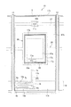
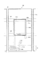
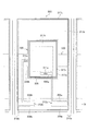
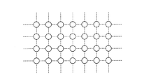
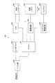
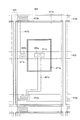
図1は、本実施の形態に係るアクティブマトリクス基板の構成を示す透視平面図である。同図に示されるように、本アクティブマトリクス基板10は、マトリクス状に配された画素領域5と、互いに直交する走査信号線16(列方向 図中左右方向)およびデータ信号線15(行方向 図中上下方向)と、第1保持容量配線20と、第2保持容量配線21とを備える。
FIG. 1 is a perspective plan view showing the configuration of the active matrix substrate according to the present embodiment. As shown in the figure, the
画素領域5には、第1のTFT(薄膜トランジスタ)12aと、第2のTFT12bと、第1副画素電極17aと、第2副画素電極17bとが形成される。
In the
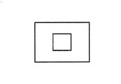
第2副画素電極17bは、長方形を一部刳り抜いた形状を有し、その外枠17xが大きな長方形、その内枠(刳り抜いた部分の外周)17yが小さな長方形となっている。そして、この内枠17yの内側に長方形形状の第1副画素電極17aが設けられている。すなわち、本アクティブマトリクス基板は、長方形形状の第1副画素電極17aを第2副画素電極17bが取り囲む構成である。
The
第1副画素電極17aの外枠17zと第2副画素電極の内枠17yとの間は間隙領域26となっており、この間隙領域26並びに第1副画素電極17aの外枠近傍領域および第2副画素電極17bの内枠近傍領域と重畳するように、第1保持容量配線20が額縁状に引き回されている。さらに、この第1保持容量配線20および第1副画素電極17aと重畳するように保持容量上電極30aが設けられ、この保持容量上電極30aと第1副画素電極17aとがコンタクトホール11aによって接続されている。なお、第2副画素電極17bの下端部(行方向の一方のエッジ)は、列方向(図中左右方向)に走る走査信号線16と重畳する。この構成では、第1保持容量配線20によって、高輝度領域47a(第1の輝度領域)と低輝度領域47b(第2の輝度領域)との間に、額縁状の黒表示領域(最低輝度領域)が形成される。
A
第1および第2のTFT12a・12bは、各信号線(15・16)の交点近傍に形成され、第1のTFT12aのソース電極9aおよび第2のTFT12bのソース電極9bはともにデータ信号線15に接続される。また、第1のTFT12aのドレイン電極8aは、ドレイン引き出し配線7aを介して保持容量上電極30aに接続され、第2のTFT12bのドレイン電極8bはドレイン引き出し配線7bおよびコンタクトホール11bを介して第2副画素電極17bに接続されている。
The first and
また、第2保持容量配線21は、第2副画素電極17bの上半分の部分(第1副画素電極17aをはさんで各TFT12a・12bの反対側)を列方向(図中左右方向)に横切るように形成され、この第2保持容量配線21および第2副画素電極17bに重畳するように保持容量上電極30bが設けられる。この保持容量上電極30bは、コンタクトホール11cを介して第2副画素電極17bに接続されている。
The second
図1では、第1保持容量配線20が間隙領域26並びに第1副画素電極17aの外枠近傍領域および第2副画素電極17bの内枠近傍領域と重畳するように額縁状に引き回されているが、これに限定されない。例えば、図28に示す画素領域5’のように、第1および第2の保持容量配線20’・21’を、第1副画素電極17aを挟むように列方向(図中左右方向)に沿って形成してもよい。なお、第1のTFT12aのドレイン電極は、第1副画素電極17a下を通過するドレイン引き出し配線7a’を介して、第1保持容量配線20’上に形成された保持容量上電極30aに接続される。さらに、このドレイン引き出し配線7a’は、コンタクトホール11aを介して第1副画素電極17aに接続される。また、第2のTFT12bのドレイン電極は、ドレイン引き出し配線7b’を介して、第2保持容量配線21’上に形成された保持容量上電極30bに接続される。さらに、この保持容量上電極30bは、コンタクトホール11bを介して第2副画素電極17bに接続される。この図28の構成では、高輝度領域47aと低輝度領域47bとの間に遮光体による最低輝度領域が形成されないため、高輝度領域47aと低輝度領域47bとが隣接するような構成となる。
In FIG. 1, the first
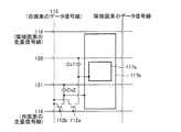
図1に示す構成によって、図2に示す回路が実現される。すなわち、第1副画素電極17aが第1のTFT12aを介してデータ信号線15に接続され、第2副画素電極17bが第2のTFT12bを介してデータ信号線15に接続される。なお、第1および第2のTFT12a・12bのゲートはともに走査信号線16に接続される。また、第1副画素電極17aに接続された保持容量上電極30aと第1保持容量配線20との間で保持容量Cs1が形成され、第2副画素電極17bに接続された保持容量上電極30bと第2保持容量配線21との間で保持容量Cs2が形成される。
The circuit shown in FIG. 2 is realized by the configuration shown in FIG. That is, the
なお、後述するように、図2の第1保持容量配線20および第2保持容量配線21には、互いに位相の異なるCs信号(補助容量対向電圧)が供給される。ここで、各画素をドット反転駆動あるいはVライン反転駆動する場合、列方向(図中左右方向)に隣接する2つの画素に供給される信号電位が逆極性となる。したがって、このような場合には、自画素の第1保持容量配線20は隣接画素の第2保持容量配線21に接続され、自画素の第2保持容量配線21は隣接画素の第1保持容量配線20に接続される。
As will be described later, Cs signals (auxiliary capacitor counter voltage) having different phases are supplied to the first
図3は、アクティブマトリクス基板10を備えた液晶表示装置(液晶パネル)の等価回路である。同図に示されるように、第1副画素電極17a、対向電極(Vcom)、および両者間の液晶層によって第1副画素容量Csp1が構成され、第2副画素電極17b、対向電極(Vcom)、および両者間の液晶層によって第2副画素容量Csp2が構成される。
FIG. 3 is an equivalent circuit of a liquid crystal display device (liquid crystal panel) including the
以下に、本実施の形態に係る液晶表示装置の駆動方法を説明する。 Hereinafter, a driving method of the liquid crystal display device according to the present embodiment will be described.
本実施の形態では、第1副画素電極とこれを取り囲む第2副画素電極に、共通のデータ信号線から表示信号電圧を供給しておき、その後各TFTをオフ状態にした後に第1保持容量配線および第2保持容量配線の電圧を相互に異なるように変化させる。これにより、1つの画素内に、第1副画素容量Csp1による高輝度領域と、これを取り囲む、第2副画素容量Csp2による低輝度領域とを形成する。この構成では、2つの副画素電極に1本のデータ信号線から表示信号電圧を供給するため、データ信号線の数やこれらを駆動するソースドライバの数を増加させる必要がないという利点がある。 In the present embodiment, a display signal voltage is supplied from a common data signal line to the first subpixel electrode and the second subpixel electrode surrounding the first subpixel electrode, and then each TFT is turned off before the first storage capacitor. The voltages of the wiring and the second storage capacitor wiring are changed to be different from each other. As a result, a high luminance region by the first subpixel capacitor Csp1 and a low luminance region by the second subpixel capacitor Csp2 surrounding the first subpixel capacitor Csp1 are formed in one pixel. In this configuration, since the display signal voltage is supplied from one data signal line to the two subpixel electrodes, there is an advantage that it is not necessary to increase the number of data signal lines and the number of source drivers for driving them.
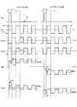
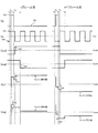
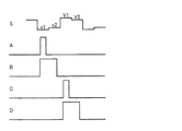
図13は、図3に示す回路の各部の電圧を示すタイミングチャートである。なお、Vgは走査信号線(第1および第2のTFTのゲート電極)の電圧、Vsはデータ信号線の電圧(ソース電圧)、Vcs1は第1保持容量配線の電圧、Vcs2は第2保持容量配線の電圧、Vlc1は第1副画素電極の電圧、Vlc2は第1副画素電極の電圧とする。なお、液晶表示装置においては、液晶が分極しないよう、一般にフレーム反転、ライン反転、ドット反転といった交流駆動を行う。すなわち、nフレーム目にソース電圧の中央値Vscに対してプラス極性のソース電圧(Vsp)を与え、次の(n+1)フレーム目ではVscに対してマイナス極性のソース電圧(Vsn)を与え、かつフレームごとにドット反転を行う。また、第1保持容量配線の電圧および第2保持容量配線の電圧を振幅電圧Vadで振幅させるとともに、両者の位相を180度ずらす。 FIG. 13 is a timing chart showing voltages at various parts of the circuit shown in FIG. Vg is the voltage of the scanning signal line (gate electrodes of the first and second TFTs), Vs is the voltage of the data signal line (source voltage), Vcs1 is the voltage of the first storage capacitor line, and Vcs2 is the second storage capacitor. The voltage of the wiring, Vlc1 is the voltage of the first subpixel electrode, and Vlc2 is the voltage of the first subpixel electrode. In the liquid crystal display device, AC driving such as frame inversion, line inversion, and dot inversion is generally performed so that the liquid crystal is not polarized. That is, a positive polarity source voltage (Vsp) is given to the median source voltage Vsc in the nth frame, a negative polarity source voltage (Vsn) is given to Vsc in the next (n + 1) th frame, and Perform dot inversion for each frame. Further, the voltage of the first storage capacitor line and the voltage of the second storage capacitor line are amplified by the amplitude voltage Vad, and the phases of both are shifted by 180 degrees.
図13のnフレームにおける各電圧波形の経時変化を説明する。 The temporal change of each voltage waveform in the n frame of FIG. 13 will be described.
まず、時刻T0で、Vcs1=Vcom−Vad、Vcs2=Vcom+Vadとする。なお、Vcomは対向電極の電圧である。 First, at time T0, Vcs1 = Vcom−Vad and Vcs2 = Vcom + Vad. Vcom is the voltage of the counter electrode.
時刻T1で、VgがVgLからVgHに変化し、各TFTがともにON状態となる。この結果、Vlc1およびVlc2がVspに上昇し、保持容量Cs1・Cs2および副画素容量Csp1・Csp2が充電される。 At time T1, Vg changes from VgL to VgH, and both TFTs are turned on. As a result, Vlc1 and Vlc2 rise to Vsp, and the storage capacitors Cs1 and Cs2 and the sub-pixel capacitors Csp1 and Csp2 are charged.
時刻T2で、VgがVgHからVgLに変化し、各TFTがOFF状態となって、保持容量Cs1・Cs2および副画素容量Csp1・Csp2がデータ信号線から電気的に絶縁される。なお、この直後に寄生容量等の影響によって引き込み現象が発生し、Vlc1=Vsp−Vd1、Vlc2=Vsp−Vd2となる。 At time T2, Vg changes from VgH to VgL, each TFT is turned off, and the storage capacitors Cs1 and Cs2 and the sub-pixel capacitors Csp1 and Csp2 are electrically insulated from the data signal line. Immediately after this, a pull-in phenomenon occurs due to the influence of parasitic capacitance or the like, and Vlc1 = Vsp−Vd1 and Vlc2 = Vsp−Vd2.
時刻T3では、Vcs1がVcom−VadからVcom+Vadへ変化し、Vcs2がVcom+VadからVcom−Vadへ変化する。この結果、Vlc1=Vsp−Vd1+2×K×Vad、Vlc2=Vsp−Vd2−2×K×Vadとなる。ここで、K=Ccs/(Clc+Ccs)であり、Ccsは各保持容量(Cs1・Cs2)の容量値、Clcは各副画素容量(Csp1・Csp2)の容量値とする。
At time T3, Vcs1 changes from Vcom−Vad to Vcom + Vad, and Vcs2 changes from Vcom + Vad to Vcom−Vad. As a result, Vlc1 = Vsp−
時刻T4では、Vcs1がVcom+VadからVcom−Vadへ変化し、Vcs2がVcom−VadからVcom+Vadへ変化する。この結果、Vlc1=Vsp−Vd1、Vlc2=Vsp−Vd2となる。 At time T4, Vcs1 changes from Vcom + Vad to Vcom−Vad, and Vcs2 changes from Vcom−Vad to Vcom + Vad. As a result, Vlc1 = Vsp−Vd1 and Vlc2 = Vsp−Vd2.
時刻T5では、Vcs1がVcom−VadからVcom+Vadへ変化し、Vcs2がVcom+VadからVcom−Vadへ変化する。この結果、Vlc1=Vsp−Vd1+2×K×Vad、Vlc2=Vsp−Vd2−2×K×Vadとなる。
At time T5, Vcs1 changes from Vcom−Vad to Vcom + Vad, and Vcs2 changes from Vcom + Vad to Vcom−Vad. As a result, Vlc1 = Vsp−
後は、次にVg=Vghとなり書き込みが行われるまで、水平走査期間1Hの整数倍ごとに、時刻T4・T5が繰り返される。したがって、Vlc1の実効値は、Vsp−Vd1+K×Vadとなり、Vlc2の実効値は、Vsp−Vd2−K×Vadとなる。 Thereafter, time T4 and T5 are repeated every integer multiple of the horizontal scanning period 1H until Vg = Vgh and writing is performed. Therefore, the effective value of Vlc1 is Vsp−Vd1 + K × Vad, and the effective value of Vlc2 is Vsp−Vd2−K × Vad.
以上から、nフレーム目において各副画素容量(第1副画素容量Csp1・第2副画素容量Csp2)にかかる実効電圧(V1・V2)は、V1=Vsp−Vd1+K×Vad−Vcom、V2=Vsp−Vd2−K×Vad−Vcomとなるため、1つの画素内に、第1副画素容量Csp1による高輝度領域と、これを取り囲む、第2副画素容量Csp2による低輝度領域とが形成される。 From the above, the effective voltage (V1 · V2) applied to each subpixel capacitor (first subpixel capacitor Csp1 and second subpixel capacitor Csp2) in the nth frame is V1 = Vsp−Vd1 + K × Vad−Vcom, V2 = Vsp. Since −Vd2−K × Vad−Vcom, a high luminance region by the first subpixel capacitor Csp1 and a low luminance region by the second subpixel capacitor Csp2 surrounding the first subpixel capacitor Csp1 are formed in one pixel.
次に、n+1フレームにおける各電圧波形の経時変化を説明する。 Next, a change with time of each voltage waveform in the (n + 1) th frame will be described.
まず、時刻T0で、Vcs1=Vcom+Vad、Vcs2=Vcom−Vadとする。なお、Vcomは対向電極の電圧である。 First, at time T0, Vcs1 = Vcom + Vad and Vcs2 = Vcom−Vad. Vcom is the voltage of the counter electrode.
時刻T1で、VgがVgLからVgHに変化し、各TFTがともにON状態となる。この結果、Vlc1およびVlc2がVsnに低下し、保持容量Cs1・Cs2および副画素容量Csp1・Csp2が充電される。 At time T1, Vg changes from VgL to VgH, and both TFTs are turned on. As a result, Vlc1 and Vlc2 are reduced to Vsn, and the holding capacitors Cs1 and Cs2 and the sub-pixel capacitors Csp1 and Csp2 are charged.
時刻T2で、VgがVgHからVgLに変化し、各TFTがOFF状態となって、保持容量Cs1・Cs2および副画素容量Csp1・Csp2がデータ信号線から電気的に絶縁される。なお、この直後に寄生容量等の影響によって引き込み現象が発生し、Vlc1=Vsn−Vd1、Vlc2=Vsn−Vd2となる。 At time T2, Vg changes from VgH to VgL, each TFT is turned off, and the storage capacitors Cs1 and Cs2 and the sub-pixel capacitors Csp1 and Csp2 are electrically insulated from the data signal line. Immediately after this, a pull-in phenomenon occurs due to the influence of the parasitic capacitance and the like, and Vlc1 = Vsn−Vd1, and Vlc2 = Vsn−Vd2.
時刻T3では、Vcs1がVcom+VadからVcom−Vadへ変化し、Vcs2がVcom−VadからVcom+Vadへ変化する。この結果、Vlc1=Vsn−Vd1−2×K×Vad、Vlc2=Vsn−Vd2+2×K×Vadとなる。ここで、K=Ccs/(Clc+Ccs)であり、Ccsは各保持容量(Cs1・Cs2)の容量値、Clcは各副画素容量(Csp1・Csp2)の容量値とする。
At time T3, Vcs1 changes from Vcom + Vad to Vcom−Vad, and Vcs2 changes from Vcom−Vad to Vcom + Vad. As a result, Vlc1 = Vsn−Vd1-2 × K × Vad and Vlc2 = Vsn−
時刻T4では、Vcs1がVcom−VadからVcom+Vadへ変化し、Vcs2がVcom+VadからVcom−Vadへ変化する。この結果、Vlc1=Vsn+Vd1、Vlc2=Vsn+Vd2となる。 At time T4, Vcs1 changes from Vcom−Vad to Vcom + Vad, and Vcs2 changes from Vcom + Vad to Vcom−Vad. As a result, Vlc1 = Vsn + Vd1, and Vlc2 = Vsn + Vd2.
時刻T5では、Vcs1がVcom+VadからVcom−Vadへ変化し、Vcs2がVcom−VadからVcom+Vadへ変化する。この結果、Vlc1=Vsn−Vd1−2×K×Vad、Vlc2=Vsn−Vd2+2×K×Vadとなる。
At time T5, Vcs1 changes from Vcom + Vad to Vcom−Vad, and Vcs2 changes from Vcom−Vad to Vcom + Vad. As a result, Vlc1 = Vsn−Vd1-2 × K × Vad and Vlc2 = Vsn−
後は、次にVg=Vghとなり書き込みが行われるまで、水平走査期間1Hの整数倍ごとに、時刻T4・T5が繰り返される。したがって、Vlc1の実効値は、Vsn−Vd1−K×Vadとなり、Vlc2の実効値は、Vsn−Vd2+K×Vadとなる。 Thereafter, time T4 and T5 are repeated every integer multiple of the horizontal scanning period 1H until Vg = Vgh and writing is performed. Therefore, the effective value of Vlc1 is Vsn−Vd1−K × Vad, and the effective value of Vlc2 is Vsn−Vd2 + K × Vad.
以上から、nフレーム目において各副画素容量(Csp1・Csp2)にかかる実効電圧(V1・V2)は、V1=Vsn−Vd1−K×Vad−Vcom、V2=Vsn−Vd2+K×Vad−Vcomとなるため、1つの画素内に、第1副画素容量Csp1による高輝度領域と、これを取り囲む、第2副画素容量Csp2による低輝度領域とが形成される。 From the above, the effective voltages (V1 · V2) applied to the sub-pixel capacitors (Csp1 · Csp2) in the nth frame are V1 = Vsn−Vd1−K × Vad−Vcom and V2 = Vsn−Vd2 + K × Vad−Vcom. Therefore, a high luminance region by the first subpixel capacitor Csp1 and a low luminance region by the second subpixel capacitor Csp2 surrounding the first subpixel capacitor Csp1 are formed in one pixel.
また、図35に示すように、Vcs1を、T2でVgが「L」となった(各TFT12a・12bがオフした)直後のT3で「High」になったまま(あるいは「Low」になったまま)の波形とし、同様に、Vcs2を、T2でVgが「L」となった直後のT3で「Low」になったまま(あるいは「High」になったまま)の波形とすることもできる。すなわち、各トランジスタがオフされた後に、Vcs1を突き上げて該フレームではこの突き上げたままの状態を維持するとともに、Vcs1の突き上げと同期してVcs2を突き下げて該フレームではこの突き下げたままの状態を維持するような電位制御を行うか、あるいは、各トランジスタがオフされた後に、Vcs1を突き下げて該フレームではこの突き下げたままの状態を維持するとともに、Vcs1の突き下げと同期してVcs2を突き上げて該フレームではこの突き上げたままの状態を維持するような電位制御を行う。この図35に示す電位制御は、各保持容量配線を上下(データ信号線に沿った方向)に隣接する画素同士で共有しない構成(図1・図4・図5等)に適用可能であり、Vcs1およびVcs2波形のなまりがドレイン実効電位に与える影響が小さくなるため、輝度ムラの低減に有効である。
Further, as shown in FIG. 35, Vcs1 remains “High” at T3 immediately after Tg2 when Vg becomes “L” (
さらに、図31のように、Vcs1を、T2でVgが「L」となった(各TFT12a・12bがオフした)直後のT3で「High」になったまま(あるいは「Low」になったまま)の波形とし、Vcs2を、T3から1水平期間(1H)後のT4で「Low」になったまま(あるいは「High」になったまま)の波形とすることもできる。すなわち、各トランジスタがオフされた後に、Vcs1を突き上げて該フレームではこの突き上げたままの状態を維持するとともに、Vcs1の突き上げから1H期間ずらしてVcs2を突き下げて該フレームではこの突き下げたままの状態を維持するような電位制御を行うか、あるいは、各トランジスタがオフされた後に、Vcs1を突き下げて該フレームではこの突き下げたままの状態を維持するとともに、Vcs1の突き下げから1H期間ずらしてVcs2を突き上げて該フレームではこの突き上げたままの状態を維持するような電位制御を行う。この図31に示す電位制御は、各保持容量配線を上下に隣接する画素同士で共有しない構成(図1等)はもちろん、各保持容量配線を上下に隣接する画素同士で共有する構成(図8)にも適用できるという利点がある。
Further, as shown in FIG. 31, Vcs1 remains “High” (or remains “Low” at T3 immediately after Vg becomes “L” at T2 (
図31のnフレームにおける各電圧波形の経時変化を説明する。 A time-dependent change of each voltage waveform in the n frame of FIG. 31 will be described.
まず、時刻T0で、Vcs1=Vcom−Vad、Vcs2=Vcom+Vadとする。なお、Vcomは対向電極の電圧である。 First, at time T0, Vcs1 = Vcom−Vad and Vcs2 = Vcom + Vad. Vcom is the voltage of the counter electrode.
時刻T1で、VgがVgLからVgHに変化し、各TFTがともにON状態となる。この結果、Vlc1およびVlc2がVspに上昇し、保持容量Cs1・Cs2および副画素容量Csp1・Csp2が充電される。 At time T1, Vg changes from VgL to VgH, and both TFTs are turned on. As a result, Vlc1 and Vlc2 rise to Vsp, and the storage capacitors Cs1 and Cs2 and the sub-pixel capacitors Csp1 and Csp2 are charged.
時刻T2で、VgがVgHからVgLに変化し、各TFTがOFF状態となって、保持容量Cs1・Cs2および副画素容量Csp1・Csp2がデータ信号線から電気的に絶縁される。なお、この直後に寄生容量等の影響によって引き込み現象が発生し、Vlc1=Vsp−Vd1、Vlc2=Vsp−Vd2となる。 At time T2, Vg changes from VgH to VgL, each TFT is turned off, and the storage capacitors Cs1 and Cs2 and the sub-pixel capacitors Csp1 and Csp2 are electrically insulated from the data signal line. Immediately after this, a pull-in phenomenon occurs due to the influence of parasitic capacitance or the like, and Vlc1 = Vsp−Vd1 and Vlc2 = Vsp−Vd2.
時刻T3では、Vcs1がVcom−VadからVcom+Vadへ変化する。時刻T4では(T3の1H後)、Vcs2がVcom+VadからVcom−Vadへ変化する。この結果、Vlc1=Vsp−Vd1+2×K×Vad、Vlc2=Vsp−Vd2−2×K×Vadとなる。ここで、K=Ccs/(Clc+Ccs)であり、Ccsは各保持容量(Cs1・Cs2)の容量値、Clcは各副画素容量(Csp1・Csp2)の容量値とする。
At time T3, Vcs1 changes from Vcom−Vad to Vcom + Vad. At time T4 (1H after T3), Vcs2 changes from Vcom + Vad to Vcom−Vad. As a result, Vlc1 = Vsp−
以上から、nフレーム目において各副画素容量(第1副画素容量Csp1・第2副画素容量Csp2)にかかる実効電圧(V1・V2)は、V1=Vsp−Vd1+2×K×Vad−Vcom、V2=Vsp−Vd2−2×K×Vad−Vcomとなるため、1つの画素内に、第1副画素容量Csp1による明副画素と、第2副画素容量Csp2による暗副画素とが形成される。
From the above, the effective voltage (V1 · V2) applied to each subpixel capacitor (first subpixel capacitor Csp1 and second subpixel capacitor Csp2) in the nth frame is V1 = Vsp−
こうすれば、Vcs1およびVcs2波形のなまりがドレイン実効電位に与える影響が小さくなり、輝度ムラの低減に有効である。 In this way, the influence of the rounds of the Vcs1 and Vcs2 waveforms on the effective drain potential is reduced, which is effective in reducing luminance unevenness.
ここで、本構成における高輝度領域と低輝度領域の輝度分配の一例を図26に示す。なお、256階調表示とし、低輝度領域と高輝度領域の面積比を1:3とする。グラフa・bに示されるように、128階調付近までは、低輝度領域の輝度(単位面積あたりの光量)を0(最小輝度)としておき、階調増加に伴って高輝度領域の輝度(単位面積あたりの光量)を0から0.85(最大輝度を1とする)まで増加させる。また、128階調付近〜255階調までは、グラフa・グラフbに示されるように、階調増加に伴って高輝度領域の輝度を0.85から1.0まで逓増させる一方で低輝度領域の輝度を0から1.0まで増加させる。この低輝度領域および高輝度領域それぞれの輝度を面積積分し、合算したものが画素全体の輝度総和(グラフc=γ特性)となる。 Here, FIG. 26 shows an example of luminance distribution between the high luminance region and the low luminance region in this configuration. Note that 256 gradation display is used, and the area ratio between the low luminance region and the high luminance region is 1: 3. As shown in the graphs a and b, the brightness of the low brightness area (light quantity per unit area) is set to 0 (minimum brightness) until the vicinity of 128 gradations, and the brightness ( (Light quantity per unit area) is increased from 0 to 0.85 (maximum luminance is 1). Further, from the vicinity of the 128th gradation to the 255th gradation, as shown in the graphs a and b, the luminance in the high luminance region is gradually increased from 0.85 to 1.0 as the gradation is increased, while the luminance is low. Increase the brightness of the region from 0 to 1.0. The luminance total of the entire pixel (graph c = γ characteristic) is obtained by integrating the luminance of each of the low luminance region and the high luminance region.
このように、本実施の形態に係る液晶表示装置では、各画素に、高輝度領域とこれを取り囲む低輝度領域とを形成することが可能である。以下では、各画素に、高輝度領域とこれを取り囲む低輝度領域とを形成することによって、空間周波数の高い映像を鮮明に表示できる点について説明する。 As described above, in the liquid crystal display device according to this embodiment, each pixel can be formed with a high luminance region and a low luminance region surrounding the high luminance region. Hereinafter, it will be described that an image having a high spatial frequency can be clearly displayed by forming a high luminance region and a low luminance region surrounding the high luminance region in each pixel.
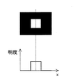
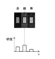
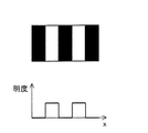
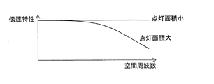
図21(a)に空間周波数の低い映像の模式図を示し、図21(b)に空間周波数の高い映像の模式図を示す。ここで、映像信号としてサイン波形を入力したときの振幅とディスプレイに出力された振幅との比を伝達特性とする。また、図22(a)は、点灯領域が大きい画素をマトリクス状に配した表示装置の模式図であり、図22(b)は、点灯領域が小さい画素をマトリクス状に配した表示装置の模式図である。さらに、図23は、図22(a)に示す表示装置の伝達特性、および図22(b)に示す表示装置の伝達特性を示す。 FIG. 21A shows a schematic diagram of an image with a low spatial frequency, and FIG. 21B shows a schematic diagram of an image with a high spatial frequency. Here, the ratio of the amplitude when a sine waveform is input as a video signal and the amplitude output to the display is defined as a transfer characteristic. FIG. 22A is a schematic diagram of a display device in which pixels with a large lighting area are arranged in a matrix, and FIG. 22B is a schematic diagram of a display device in which pixels with a small lighting area are arranged in a matrix. FIG. Further, FIG. 23 shows the transfer characteristics of the display device shown in FIG. 22A and the transfer characteristics of the display device shown in FIG.
図23から、点灯領域が小さな表示装置の方が、点灯領域の大きな表示装置よりも伝達特性が優れている、すなわち、図21(b)に示されるような高空間周波数の映像をより鮮明に表示できることがわかる。本発明はこの原理に着目したものであり、1つの画素内に、高輝度領域とこれを取り囲む低輝度領域とを形成できる画素構成とし、画素全体の輝度総和の全部あるいはほとんどを高輝度領域で賄って(光放射を画素中央に集中させて)(表示の大半を占める)中間調表示を行う。これにより、高空間周波数領域における伝達特性が大幅に向上し、空間周波数の高い映像を鮮明に表示することができる。 From FIG. 23, a display device with a small lighting area has better transfer characteristics than a display device with a large lighting area, that is, a higher spatial frequency image as shown in FIG. It can be seen that it can be displayed. The present invention pays attention to this principle, and has a pixel configuration capable of forming a high-luminance region and a low-luminance region surrounding the same in one pixel, and all or most of the total luminance of the entire pixel in the high-luminance region. Covered (concentrates light emission at the center of the pixel) and performs halftone display (occupies most of the display). Thereby, the transfer characteristic in the high spatial frequency region is greatly improved, and an image with a high spatial frequency can be clearly displayed.
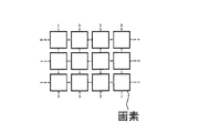
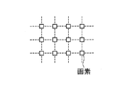
また、本アクティブマトリクス基板では、図15(a)に示すように、各画素の中央部に高輝度領域が形成され、各画素における高輝度領域の行方向(図中上下方向)の位置が画素間で揃っているため、図15(b)のように各画素における高輝度領域の行方向の位置が画素間でずれている構成と比較して、図14に模式的に示されような映像信号をよりきれいに表示できる。 Further, in the present active matrix substrate, as shown in FIG. 15A, a high luminance region is formed at the center of each pixel, and the position of each pixel in the row direction (vertical direction in the drawing) is the pixel. Compared with the configuration in which the position in the row direction of the high luminance region in each pixel is shifted between the pixels as shown in FIG. 15B, the image as schematically shown in FIG. The signal can be displayed more clearly.
また、図1に示す本アクティブマトリクス基板は、第1および第2の画素電極間の領域(間隙領域26)と重畳するように、第1の保持容量配線20が額縁状に引き回されている。したがって、本アクティブマトリクス基板を備えた液晶表示装置において、間隙領域26から光が漏れ、コントラストが低下するといった現象を防止することができる。
Further, in the active matrix substrate shown in FIG. 1, the first
また、本実施の形態では、アクティブマトリクス基板自体に遮光体(第1の保持容量配線20)設けることになるため、カラーフィルタ基板に遮光体を設ける場合のように各基板を貼り合わせる際のずれによって遮光効果が低下してしまうといった問題も起こらない。 Further, in this embodiment, since the light shielding body (first storage capacitor wiring 20) is provided on the active matrix substrate itself, the shift when the substrates are bonded as in the case where the light shielding body is provided on the color filter substrate. Therefore, there is no problem that the light shielding effect is lowered.
加えて、図1の構成では、1つの画素領域内において、第1の保持容量配線20が額縁状に引き回され、該第1の保持容量配線20が複数の経路を有することになるため、第1の保持容量配線の断線に対して冗長性を有している。
In addition, in the configuration of FIG. 1, the first
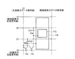
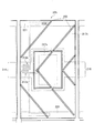
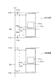
本アクティブマトリクス基板を図4に示すように構成することもできる。すなわち、画素領域105には、第1のTFT(薄膜トランジスタ)112aと、第2のTFT112bと、第1副画素電極117aと、第2副画素電極117bとが形成される。
The present active matrix substrate can also be configured as shown in FIG. That is, in the
第2副画素電極117bは、長方形を一部刳り抜いた形状を有し、その外枠117xが大きな長方形、その内枠(刳り抜いた部分の外周)117yが小さな長方形となっている。そして、この内枠117yの内側に長方形形状の第1副画素電極117aが設けられている。すなわち、本実施の形態は、長方形形状の第1副画素電極117aを第2副画素電極117bが取り囲む構成である。
The
第1副画素電極117aの外枠117zと第2副画素電極の内枠117yとの間は間隙領域(126a〜126d)となっている。この間隙領域は額縁状であり、列方向(図中左右方向)に伸びた領域126aおよび領域126bと、行方向(図中上下方向)に伸びた領域126cおよび領域126dとからなる。ここで、領域126a並びに第1副画素電極117aの外枠近傍領域および第2副画素電極117bの内枠近傍領域と重畳するように、第1保持容量配線121が形成され、領域126b並びに第1副画素電極117aの外枠近傍領域および第2副画素電極117bの内枠近傍領域と重畳するように、第2保持容量配線120が形成されている。さらに、この第1保持容量配線120および第1副画素電極117aと重畳するように保持容量上電極130aが設けられ、この保持容量上電極130aと第1副画素電極117aとがコンタクトホール111aによって接続されている。また、第2保持容量配線121および第2副画素電極117bに重畳するように保持容量上電極130bが設けられる。
A gap region (126a to 126d) is formed between the
第1および第2のTFT112a・112bは、各信号線(15・16)の交点近傍に形成され、第1のTFT112aのソース電極109aおよび第2のTFT112bのソース電極109bはともにデータ信号線15に接続される。第1のTFT112aのドレイン電極108aは、ドレイン引き出し配線107aを介して保持容量上電極130aに接続される。ここで、ドレイン引き出し配線107aは行方向(図中上下方向)に伸びる領域126c並びに第1副画素電極117aの外枠近傍領域および第2副画素電極117bの内枠近傍領域と重畳するように引き回されている。また、第2のTFT112bのドレイン電極108bはドレイン引き出し配線107bおよびコンタクトホール111bを介して第2副画素電極117bに接続されている。さらに、ドレイン引き出し配線107bは、行方向(図中上下方向)に伸びる領域126d並びに第1副画素電極117aの外枠近傍領域および第2副画素電極117bの内枠近傍領域と重畳するように引き回され、保持容量上電極130bに接続されている。
The first and
なお、図5に示すように、開口率向上のためにこのドレイン引き出し配線107bの領域126dと重畳しない部分を削除し、第2副画素電極117bと保持容量上電極130bとをコンタクトホール111cによって接続しておくこともできる。
As shown in FIG. 5, in order to improve the aperture ratio, the portion of the drain lead-out
以上説明した図4・5のアクティブマトリクス基板によって図6に示す回路が実現される。また、図4・5のアクティブマトリクス基板を用いた液晶表示装置にも、図13で説明した駆動方法を用いることができる。 The circuit shown in FIG. 6 is realized by the active matrix substrate of FIGS. 4 and 5 described above. The driving method described with reference to FIG. 13 can also be used for the liquid crystal display device using the active matrix substrate of FIGS.
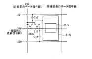
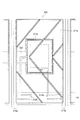
本アクティブマトリクス基板を図8に示すように構成することもできる。すなわち、画素領域205には、第1のTFT(薄膜トランジスタ)212aと、第2のTFT212bと、第1副画素電極217aと、第2副画素電極217bとが形成される。
The present active matrix substrate can also be configured as shown in FIG. That is, a first TFT (thin film transistor) 212a, a
第2副画素電極217bは、長方形を一部刳り抜いた形状を有し、その外枠217xが大きな長方形、その内枠(刳り抜いた部分の外周)217yが小さな長方形となっている。そして、この内枠217yの内側に長方形形状の第1副画素電極217aが設けられている。すなわち、本実施の形態は、長方形形状の第1副画素電極217aを第2副画素電極217bが取り囲む構成である。
The
本構成では、画素領域205の中程に走査信号線216が設けられる。画素領域205内の走査信号線216は、第1および第2のTFT212a・212bのゲート電極となる左端部216a、額縁部216b、および右端部216cの3つの部分からなる。第1および第2のTFT212a・212bは、各信号線(15・216)の交点近傍に形成され、第1のTFT212aのソース電極209aおよび第2のTFT212bのソース電極209bはともにデータ信号線15に接続される。
In this configuration, the
第1副画素電極217aの外枠217zと第2副画素電極の内枠217yとの間は間隙領域226となっており、この間隙領域226並びに第1副画素電極217aの外枠近傍領域および第2副画素電極217bの内枠近傍領域と重畳するように、走査信号線216の引き回され、これにより上記額縁部216bが形成される。第1のTFT212aのドレイン電極208aは、ドレイン引き出し配線およびコンタクトホール211aを介して第1副画素電極217aに接続される。
A
また、画素領域205の上下両端部(行方向の両エッジ)に、第1および第2保持容量配線220・221が列方向(図中左右方向)に形成される。また、第1保持容量配線220と重畳するように保持容量上電極230aが設けられ、この保持容量上電極230aは、ドレイン電極208aに接続されている。さらに、第2保持容量配線221と第2副画素電極217bとに重畳するように保持容量上電極230bが設けられ、この保持容量上電極230bは、ドレイン電極208bに接続されるとともに、コンタクトホール211bを介して第2副画素電極217bに接続されている。
In addition, first and second
図8の構成によれば、上下に隣接する画素間で第1および第2の保持容量配線220・221を共用できるため、保持容量配線の総数を減らすことができる。また、1つの画素領域内において、走査信号線216が額縁状に引き回され、該走査信号線216が複数の経路を有することになるため、走査信号線の断線に対して冗長性を有している。
According to the configuration of FIG. 8, the first and second
以上説明した図8のアクティブマトリクス基板によって図7に示す回路が実現される。また、図8のアクティブマトリクス基板を用いた液晶表示装置にも、図13で説明した駆動方法を用いることができる。 The circuit shown in FIG. 7 is realized by the active matrix substrate of FIG. 8 described above. The driving method described with reference to FIG. 13 can also be used for a liquid crystal display device using the active matrix substrate of FIG.
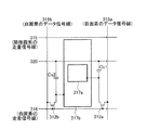
本アクティブマトリクス基板を図9に示すように構成することもできる。すなわち、画素領域305には、第1のTFT(薄膜トランジスタ)312aと、第2のTFT312bと、第1副画素電極317aと、第2副画素電極317bとが形成される。
The present active matrix substrate can also be configured as shown in FIG. That is, in the
そして、本構成では、1つの画素領域305に対して2本のデータ信号線315a・315bが設けられる。これらデータ信号線315a・315bは、画素領域305の両側端部近傍に、行方向(図中上下方向)に形成される。
In this configuration, two
第2副画素電極317bは、長方形を一部刳り抜いた形状を有し、その外枠317xが大きな長方形、その内枠(刳り抜いた部分の外周)317yが小さな長方形となっている。そして、この内枠317yの内側に長方形形状の第1副画素電極317aが設けられている。すなわち、本実施の形態は、長方形形状の第1副画素電極317aを第2副画素電極317bが取り囲む構成である。
The
第1副画素電極317aの外枠317zと第2副画素電極の内枠317yとの間は間隙領域326となっており、この間隙領域326並びに第1副画素電極317aの外枠近傍領域および第2副画素電極317bの内枠近傍領域と重畳するように、保持容量配線320が額縁状に引き回されている。さらに、この保持容量配線320および第1副画素電極317aと重畳するように保持容量上電極330aが設けられ、この保持容量上電極330aと第1副画素電極317aとがコンタクトホール311aによって接続されている。また、この保持容量配線320および第2副画素電極317bと重畳するように保持容量上電極330bが設けられ、この保持容量上電極330bと第2副画素電極317bとがコンタクトホール311bによって接続されている。
A
第1のTFT312aは、走査信号線と一方のデータ信号線315aとの交点近傍に形成され、第1のTFT312aのソース電極309aはデータ信号線315aに接続され、第1のTFT312aのドレイン電極308aは、ドレイン引き出し配線を介して保持容量上電極330aに接続される。また、第1のTFT312bは、走査信号線ともう一方のデータ信号線315bの交点近傍に形成され、第1のTFT312bのソース電極309bはデータ信号線315bに接続され、第1のTFT312bのドレイン電極308bは、ドレイン引き出し配線を介して保持容量上電極330bに接続される。
The
以上説明した図9のアクティブマトリクス基板によって図12に示す回路が実現される。ここで、各画素に配される2本のデータ信号線315a・315bは互いに独立に駆動され、例えば、液晶コントローラによって制御されるソースドライバから別々に信号電位が与えられる。
The circuit shown in FIG. 12 is realized by the active matrix substrate of FIG. 9 described above. Here, the two
ここで、本構成における高輝度領域と低輝度領域の輝度(単位面積あたりの光量)分配の一例を図27に示す。なお、256階調表示とし、低輝度領域と高輝度領域の面積比を1:3とする。グラフa・bに示されるように、128階調付近までは、低輝度領域の輝度を0(規格化した最小輝度)としておき、階調増加に伴って高輝度領域の輝度を0から1.0(規格化した最大輝度)まで増加させる。また、128階調付近〜255階調までは、グラフa・bに示されるように、高輝度領域の輝度を1.0にしておき、階調増加に伴って低輝度領域の輝度を0から1.0まで増加させる。この低輝度領域および高輝度領域の各輝度を面積積分し、合算したものが画素全体の輝度総和(グラフc=γ特性)となる。 Here, FIG. 27 shows an example of luminance (light quantity per unit area) distribution between the high luminance region and the low luminance region in this configuration. Note that 256 gradation display is used, and the area ratio between the low luminance region and the high luminance region is 1: 3. As shown in the graphs a and b, the luminance of the low luminance region is set to 0 (normalized minimum luminance) until the vicinity of 128 gradations, and the luminance of the high luminance region is changed from 0 to 1 as the gradation is increased. Increase to 0 (normalized maximum brightness). Further, from the vicinity of 128 gradations to 255 gradations, as shown in the graphs a and b, the luminance of the high luminance region is set to 1.0, and the luminance of the low luminance region is changed from 0 as the gradation is increased. Increase to 1.0. The luminances of the entire pixel are summed (graph c = γ characteristic) by integrating the luminances of the low luminance region and high luminance region.
また、図10に示すように、図8のアクティブマトリクス基板をMVA(Multi−domain Vertical Alignment)構成とすることもできる。すなわち、第1および第2副画素電極217a・217bに、液晶分子の配向を制御するためのスリット(液晶分子配向制御用スリット)255を横V字形状(V字を90度回転させた形状)に設ける。このMVA構成は、アクティブマトリクス基板の画素電極にスリット(電極切除パターン)を設けるとともに、対向基板の対向電極に液晶分子配向制御用突起(リブ)を設け、これによって形成されるフリンジフィールド(Fringe Field)を利用するものである。このフリンジフィールドによって液晶分子の配向方向を複数方向に分散させることができ、広視野角が実現される。同様に、図9のアクティブマトリクス基板をMVA構成とすることもできる(図11参照)。
Further, as shown in FIG. 10, the active matrix substrate of FIG. 8 may have an MVA (Multi-domain Vertical Alignment) configuration. That is, a slit (liquid crystal molecule alignment control slit) 255 for controlling the alignment of liquid crystal molecules is formed in the first and
本実施の形態に係るアクティブマトリクス基板を図29のように構成することもできる。図29に示されるアクティブマトリクス基板は、マトリクス状に配された画素領域405と、画素領域の下端部および上端部を列方向(図中左右方向)に走る第1および第2の走査信号線416a・416bと、行方向(図中上下方向)に走るデータ信号線415と、保持容量配線420とを備える。
The active matrix substrate according to this embodiment can also be configured as shown in FIG. The active matrix substrate shown in FIG. 29 includes a
画素領域405には、第1のTFT412aと、第2のTFT412bと、第1副画素電極417aと、第2副画素電極417bとが形成される。第2副画素電極417bは、長方形を一部刳り抜いた形状を有し、その外枠417xが大きな長方形、その内枠(刳り抜いた部分の外周)417yが小さな長方形となっている。そして、この内枠417yの内側に長方形形状の第1副画素電極417aが設けられている。すなわち、本実施の形態は、長方形形状の第1副画素電極417aを第2副画素電極417bが取り囲む構成である。
In the
保持容量配線420は、画素領域中央を横切るように形成されており、保持容量配線420および第2副画素電極417bと重畳するように保持容量上電極430bが設けられ、保持容量配線420および第1副画素電極417aと重畳するように保持容量上電極430aが設けられている。
The
ここで、第1のTFT412aは、データ信号線15と第1の走査信号線16aの交点近傍に形成されており、第1の走査信号線16aが第1のTFT412aのゲート電極となっている。また、第2のTFT412bは、データ信号線15と第2の走査信号線16bの交点近傍に形成されており、第2の走査信号線16bが第2のTFT412bのゲート電極となっている。なお、第1のTFT412aのソース電極および第2のTFT412bのソース電極はともにデータ信号線415に接続される。
Here, the
また、第1のTFT412aのドレイン電極は、ドレイン引き出し配線407aを介して保持容量上電極430aに接続され、この保持容量上電極430aは、コンタクトホール411aを介して第1副画素電極417aに接続されている。また、第2のTFT412bのドレイン電極は、ドレイン引き出し配線407bを介して保持容量上電極430bに接続され、この保持容量上電極430bは、コンタクトホール411bを介して第2副画素電極417bに接続されている。
The drain electrode of the
上記の構成によって、図30に示す回路が実現される。すなわち、第1副画素電極417aが第1のTFT412aを介してデータ信号線415に接続され、第2副画素電極417bが第2のTFT412bを介してデータ信号線415に接続される。第1のTFT412aのゲートは第1の走査信号線416aに接続され、第2のTFT412bのゲートは第2の走査信号線416bに接続される。また、第1副画素電極417aに接続された保持容量上電極430aと保持容量配線420との間で保持容量CSが形成され、同様に、第2副画素電極417bに接続された保持容量上電極430bと保持容量配線420との間で保持容量CSが形成される。なお、第1および第2の走査信号線21には、タイミングの異なる走査信号(パルス信号)が供給される。なお、次段用の第1および第2の走査信号線をそれぞれ416cおよび416dとし、次段用の第1および第2のTFTをそれぞれ417cおよび417dとする。
With the above configuration, the circuit shown in FIG. 30 is realized. That is, the
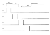
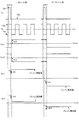
図32は、図30の回路でドット反転駆動を行う場合の各信号波形(図中Sはデータ信号線415に供給される電位信号の波形、A〜Dはそれぞれ、走査信号線416a〜416dに供給されるパルス信号の波形)である。
32 shows signal waveforms when dot inversion driving is performed in the circuit of FIG. 30 (in the figure, S is a waveform of a potential signal supplied to the data signal
同図に示されるように、一水平期間に、第1の走査信号線416a、第2の走査信号線416bの順にオンパルス(走査信号)が供給されるとともに、各オンパルスに対応して、データ信号線415に、信号電位V1・V2(ともに正極性)が供給される。なお、第1および第2の走査信号線に供給される各オンパルスは時間的に重ならない。これにより、第1のTFT412aを介して第1副画素電極417aにV1が書き込まれ、第2のTFT412bを介して第2副画素電極417bにV2が書き込まれる。さらに、これに続く一水平期間では、次段の第1の走査信号線416c、同第2の走査信号線416dの順にオンパルスが供給されるとともに、各オンパルスに対応して、データ信号線415に、信号電位v1・v2(ともに負極性)が供給される。これにより、次段の第1副画素電極417cにv1が書き込まれ、同第2副画素電極417dにv2が書き込まれる。
As shown in the figure, in one horizontal period, on-pulses (scanning signals) are supplied in the order of the first
また、図30の回路でドット反転駆動を行う場合、各信号波形を図33(図中Sはデータ信号線415に供給される電位信号の波形、A〜Dはそれぞれ、走査信号線416a〜416dに供給されるパルス信号の波形)のようにすることも可能である。
Further, when dot inversion driving is performed in the circuit of FIG. 30, each signal waveform is shown in FIG. 33 (S is a waveform of a potential signal supplied to the data signal
すなわち、一水平期間に、第1の走査信号線416a、第2の走査信号線416bにオンパルス(走査信号)が供給されるとともに、各オンパルスに対応して、データ信号線415に、信号電位v1・v2(ともに負極性)が供給される。ここで、第1の走査信号線に供給されるオンパルスと第2の走査信号線に供給されるオンパルスとを、時間的に重なる部分を有しつつパルス終端をとるタイミングが異なるように設定する。例えば、2つのオンパルスは、パルス始端をとるタイミングが同期する一方で、パルス終端をとるタイミングは第1の走査信号線416aに供給されるオンパルスが先であるようにする。例えば、2つのオンパルスがパルス終端をとるタイミングを1/2H(一水平期間の半分)だけずらす。加えて、データ信号線415に供給される電位は、各オンパルスがパルス始端をとるのと同期してあるいはそれ以前にv1となるとともに、一方のオンパルス(第1の走査信号線416aに供給されるオンパルス)が先にパルス終端をとるのと同期して、あるいはそれ以後にv1からv2に変化するようにしておく。こうすれば、第1副画素電極417aにv1が書き込まれ、第2副画素電極417bには、v1が書き込まれた後にv2が再書き込みされる。さらに、これに続く一水平期間では、次段の第1の走査信号線416c、同第2の走査信号線416dに、上記のタイミングでオンパルスが供給されるとともに、データ信号線415に、各オンパルスに対応して信号電位V1・V2(ともに正極性)が供給される(すなわち、第1の走査信号線416aに供給されるオンパルスが先にパルス終端をとるのと同期して、あるいはそれ以後にV1からV2に変化する)。これにより、次段の第1副画素電極417cにV1が書き込まれ、同第2副画素電極417dには、V1が書き込まれた後にV2が再書き込みされる。
That is, an ON pulse (scanning signal) is supplied to the first
こうすれば、第2の走査信号線416bが制御する第2のTFT412bに接続する第2の副画素電極417bには、v1(書き込むべき電位と同極性)が一旦与えられた状態で再度書き込むべき電位v2が与えられることになり、第2の副画素電極417bの充電を良好に行うことができる。特に、ドット反転駆動やHライン反転駆動のように水平期間ごとにデータ信号線415に与えられる信号電位の極性が反転する(信号電位の波形鈍りが大きい)場合や第2の副画素電極417bの面積が大きい(充電に時間がかかる)場合により効果的である。さらに、図33の駆動方法では、図32の駆動方法よりオンパルスの周期が長くなるため、走査信号の駆動周波数を抑制できるという効果もある。
In this case, the
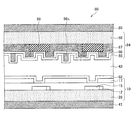
上記実施の形態で得られるアクティブマトリクス基板と、アクティブマトリクス基板の各画素に対応するようにマトリクス状に設けられた赤、緑、青のうちのいずれか1つの着色層と、各着色層の間に設けられた遮光性のブラックマトリクスからなるように形成されたカラーフィルタ基板を貼り合わせ、液晶を注入・封止することで、液晶表示パネルが形成される。 Between the active matrix substrate obtained in the above embodiment, any one colored layer of red, green, and blue provided in a matrix so as to correspond to each pixel of the active matrix substrate, and each colored layer A liquid crystal display panel is formed by laminating a color filter substrate formed of a light-shielding black matrix provided on and injecting and sealing liquid crystal.
この液晶表示パネルの構成を図34に示す。同図に示すように、本液晶パネル80は、バックライト光源側から順に、偏光板41、ガラス基板28を含む本アクティブマトリクス基板10、配向膜82、液晶層43、カラーフィルタ基板84、および偏光板85を備える。カラーフィルタ基板84は、液晶層43側から順に、配向膜85、共通(対向)電極86、着色層87(ブラックマトリクス99を含む)、ガラス基板88を備える。そして、この共通(対向)電極86に液晶分子配向制御用突起(リブ)86xが設けられている。液晶分子配向制御用突起86xは、例えば、感光性樹脂等により形成される。リブ86xの(基板面垂直方向から見たときの)平面形状としては、一定の周期でジグザクに屈曲した帯状(横V字形状)等が挙げられる。上記液晶パネルにドライバ(液晶駆動用LSI)等を接続し、偏光板やバックライトを装着することで本発明の液晶表示装置が形成される。
The configuration of this liquid crystal display panel is shown in FIG. As shown in the figure, the present
以下に、本液晶表示装置を適用したテレビジョン受信機について説明する。 Hereinafter, a television receiver to which the present liquid crystal display device is applied will be described.
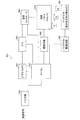
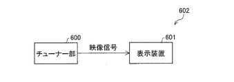
図16は、テレビジョン受信機用における液晶表示装置601の回路ブロックである。液晶表示装置601は、図16に示すように、Y/C分離回路500、ビデオクロマ回路501、A/Dコンバータ502、液晶コントローラ503、液晶パネル504、バックライト駆動回路505、バックライト506、マイコン507、階調回路508を備えた構成となっている。上記構成の液晶表示装置601において、まず、テレビ信号の入力映像信号は、Y/C分離回路500に入力され、輝度信号と色信号に分離される。輝度信号と色信号はビデオクロマ回路501にて光の3原色である、R、G、Bに変換され、さらに、このアナログRGB信号はA/Dコンバータ502により、デジタルRGB信号に変換され、液晶コントローラ503に入力される。液晶パネル504では液晶コントローラ503からのRGB信号が所定のタイミングで入力されると共に、階調回路508からのRGBそれぞれの階調電圧が供給され、画像が表示されることになる。これらの処理を含め、システム全体の制御はマイコン507が行うことになる。なお、映像信号として、テレビジョン放送に基づく映像信号、カメラにより撮像された映像信号、インターネット回線を介して供給される映像信号など、様々な映像信号に基づいて表示可能である。
FIG. 16 is a circuit block of a liquid
なお、本アクティブマトリクス基板は、フィールドシーケンシャル方式の液晶表示装置に用いることもできる。図17(a)に示すフィールドシーケンシャル方式の1つの画素は、図17(b)に示すカラーフィルタ方式の3つ画素(R・G・B)に対応し、1つの画素に3原色の3つの色(R・G・B)が連続して表示される(ある時刻には1色のみが表示される)。フィールドシーケンシャル方式の液晶表示装置では、例えば図8のような駆動が行われる。すなわち、1フレームが3分割(第1〜第3のサブフレーム)され、第1のサブフレームではRの映像信号が送られるとともに、バックライトがR(赤)に点灯し、液晶パネルにRの信号表示がなされる。同様に、第2のサブフレームではGの映像信号が送られるとともに、バックライトがG(緑)に点灯し、液晶パネルにGの信号表示がなされる。第3のサブフレームではBの映像信号が送られるとともに、バックライトがB(青)に点灯し、液晶パネルにBの信号表示がなされる。 Note that this active matrix substrate can also be used for a field sequential liquid crystal display device. One pixel of the field sequential method shown in FIG. 17A corresponds to three pixels (R, G, and B) of the color filter method shown in FIG. 17B, and three pixels of three primary colors are included in one pixel. The colors (R, G, B) are displayed continuously (only one color is displayed at a certain time). In the field sequential type liquid crystal display device, for example, driving as shown in FIG. 8 is performed. That is, one frame is divided into three (first to third subframes), an R video signal is sent in the first subframe, the backlight is lit in R (red), and the liquid crystal panel has an R A signal is displayed. Similarly, in the second subframe, a G video signal is sent, the backlight is lit in G (green), and the G signal is displayed on the liquid crystal panel. In the third sub-frame, the B video signal is transmitted, the backlight is lit in B (blue), and the B signal is displayed on the liquid crystal panel.
このフィールドシーケンシャル方式によれば、カラーフィルタを用いた構成(図19(b)に示されるように色情報の位置が各色によってずれる)と異なり、各色で色情報の位置がずれない(図19(a)のように画素中央の1箇所になる)という利点がある。ここで、図20にフィールドシーケンシャル方式の液晶表示装置の回路ブロックを示しておく。 According to this field sequential method, unlike the configuration using color filters (the position of color information is shifted by each color as shown in FIG. 19B), the position of color information is not shifted for each color (FIG. 19 ( As in a), there is an advantage that it is one place in the center of the pixel. Here, FIG. 20 shows a circuit block of a field sequential type liquid crystal display device.
本液晶表示装置601は、図24に示すように、テレビジョン放送を受信して映像信号を出力するチューナ部600と接続することにより、チューナ部600から出力された映像信号に基づいて映像(画像)表示を行うことが可能になる。この場合、液晶表示装置601とチューナ部600とでテレビジョン受像機602となる。
As shown in FIG. 24, the present liquid
液晶表示装置601を用いてテレビジョン受信機602を構成するには、例えば、図25に示すように、液晶表示装置601を第1筐体801と第2筐体806とで包み込むようにして挟持した構成となっている。第1筐体801は、液晶表示装置601で表示される映像を透過させる開口部801aが形成されている。また、第2筐体806は、液晶表示装置601の背面側を覆うものであり、該液晶表示装置601を操作するための操作用回路805が設けられるとともに、下方に支持用部材808が取り付けられている。
To configure the
なお、本発明は液晶表示装置に限定されるものではなく、例えば、カラーフィルタ基板と、カラーフィルタ基板と対向するように本発明のアクティブマトリクス基板を配置し、それら基板と基板との間に有機EL層を配置することで有機ELパネルとし、パネルの外部引き出し端子にドライバ等を接続することにより有機EL表示装置を構成することも可能である。また、液晶表示装置や有機EL表示装置以外であっても、アクティブマトリクス基板で構成される表示装置であれば、本発明は適用可能である。 The present invention is not limited to a liquid crystal display device. For example, a color filter substrate and an active matrix substrate of the present invention are disposed so as to face the color filter substrate, and an organic material is interposed between the substrates. It is possible to form an organic EL panel by disposing an EL layer, and to configure an organic EL display device by connecting a driver or the like to an external lead terminal of the panel. Further, the present invention can be applied to any display device including an active matrix substrate other than the liquid crystal display device and the organic EL display device.
本発明のアクティブマトリクス基板は、例えば液晶テレビに好適である。 The active matrix substrate of the present invention is suitable for a liquid crystal television, for example.
5 画素領域
12a・12b TFT
15 データ信号線
16 走査信号線
17a 第1の副画素電極
17b 第2の副画素電極
11a・11b コンタクトホール
20 第1の保持容量配線
21 第2の保持容量配線
5
DESCRIPTION OF
Claims (5)
走査信号線と、データ信号線と、第1および第2保持容量配線と、第1保持容量配線に重なる第1保持容量上電極と、第2保持容量配線に重なる第2保持容量上電極とが設けられ、
第1および第2副画素電極はそれぞれ、上記走査信号線に接続するトランジスタを介して上記データ信号線に接続され、
第1保持容量上電極は第1副画素電極に接続されるとともに、第2保持容量上電極は第2副画素電極に接続され、
第2副画素電極は平面的に視て内周および外周を有する形状であって、かつ第2副画素電極の内周の内側に第1副画素電極が配されていることにより、中間調を表示する時に第2輝度領域が第1輝度領域を取り囲み、上記第1および第2輝度領域の間隙には最低輝度領域が形成され、
上記第1および第2保持容量配線は、第1副画素電極と重ならないように配されていることを特徴とする表示装置。 When displaying a halftone on a pixel, the first luminance region corresponding to the first subpixel electrode corresponds to the second subpixel electrode by setting the first and second subpixel electrodes in the pixel to different effective potentials. A display device having a higher luminance than the second luminance region,
A scanning signal line, a data signal line, first and second storage capacitor lines, a first storage capacitor upper electrode overlapping the first storage capacitor line, and a second storage capacitor upper electrode overlapping the second storage capacitor line Provided,
Each of the first and second subpixel electrodes is connected to the data signal line through a transistor connected to the scanning signal line,
The first storage capacitor upper electrode is connected to the first subpixel electrode, and the second storage capacitor upper electrode is connected to the second subpixel electrode.
The second subpixel electrode has a shape having an inner periphery and an outer periphery in a plan view, and the first subpixel electrode is arranged inside the inner periphery of the second subpixel electrode, so that a halftone is obtained. When displaying, the second luminance area surrounds the first luminance area, a minimum luminance area is formed in the gap between the first and second luminance areas ,
The display device, wherein the first and second storage capacitor lines are arranged so as not to overlap the first subpixel electrode .
Priority Applications (1)
| Application Number | Priority Date | Filing Date | Title |
|---|---|---|---|
| JP2010023578A JP5073766B2 (en) | 2006-02-06 | 2010-02-04 | Display device, liquid crystal display device, television receiver |
Applications Claiming Priority (5)
| Application Number | Priority Date | Filing Date | Title |
|---|---|---|---|
| JP2006029043 | 2006-02-06 | ||
| JP2006029043 | 2006-02-06 | ||
| JP2006248558 | 2006-09-13 | ||
| JP2006248558 | 2006-09-13 | ||
| JP2010023578A JP5073766B2 (en) | 2006-02-06 | 2010-02-04 | Display device, liquid crystal display device, television receiver |
Related Parent Applications (1)
| Application Number | Title | Priority Date | Filing Date |
|---|---|---|---|
| JP2007557747A Division JPWO2007091365A1 (en) | 2006-02-06 | 2006-11-30 | Display device, active matrix substrate, liquid crystal display device, television receiver |
Publications (3)
| Publication Number | Publication Date |
|---|---|
| JP2010160493A JP2010160493A (en) | 2010-07-22 |
| JP2010160493A5 JP2010160493A5 (en) | 2010-09-02 |
| JP5073766B2 true JP5073766B2 (en) | 2012-11-14 |
Family
ID=38344972
Family Applications (2)
| Application Number | Title | Priority Date | Filing Date |
|---|---|---|---|
| JP2007557747A Pending JPWO2007091365A1 (en) | 2006-02-06 | 2006-11-30 | Display device, active matrix substrate, liquid crystal display device, television receiver |
| JP2010023578A Expired - Fee Related JP5073766B2 (en) | 2006-02-06 | 2010-02-04 | Display device, liquid crystal display device, television receiver |
Family Applications Before (1)
| Application Number | Title | Priority Date | Filing Date |
|---|---|---|---|
| JP2007557747A Pending JPWO2007091365A1 (en) | 2006-02-06 | 2006-11-30 | Display device, active matrix substrate, liquid crystal display device, television receiver |
Country Status (3)
| Country | Link |
|---|---|
| US (1) | US20090009449A1 (en) |
| JP (2) | JPWO2007091365A1 (en) |
| WO (1) | WO2007091365A1 (en) |
Families Citing this family (36)
| Publication number | Priority date | Publication date | Assignee | Title |
|---|---|---|---|---|
| KR101244332B1 (en) * | 2006-09-18 | 2013-03-18 | 삼성디스플레이 주식회사 | Display apparatus |
| TWI360010B (en) * | 2007-09-20 | 2012-03-11 | Chimei Innolux Corp | Pixel array substrate and liquid crystal display |
| KR101508639B1 (en) | 2007-11-29 | 2015-04-06 | 가부시키가이샤 한도오따이 에네루기 켄큐쇼 | Liquid crystal display device and electronic device |
| KR101448001B1 (en) * | 2008-01-29 | 2014-10-13 | 삼성디스플레이 주식회사 | Liquid crystal display |
| KR20090103461A (en) | 2008-03-28 | 2009-10-01 | 삼성전자주식회사 | Liquid crystal display |
| JP4626664B2 (en) * | 2008-03-31 | 2011-02-09 | カシオ計算機株式会社 | Liquid crystal display device |
| TWI377383B (en) * | 2008-05-05 | 2012-11-21 | Au Optronics Corp | Pixel, display and the driving method thereof |
| JP5305755B2 (en) * | 2008-06-27 | 2013-10-02 | 三菱電機株式会社 | Liquid crystal display |
| KR101540302B1 (en) * | 2008-07-09 | 2015-07-29 | 삼성디스플레이 주식회사 | Display substrate and liquid crystal display panel having the same |
| JP4706729B2 (en) | 2008-07-14 | 2011-06-22 | カシオ計算機株式会社 | Liquid crystal display device |
| KR101518327B1 (en) * | 2008-07-24 | 2015-05-11 | 삼성디스플레이 주식회사 | Liquid crystal display panel and liquid crystal display device |
| KR101595817B1 (en) | 2008-08-22 | 2016-02-22 | 삼성디스플레이 주식회사 | Liquid crystal display |
| KR101549962B1 (en) * | 2008-11-28 | 2015-09-04 | 삼성디스플레이 주식회사 | Liquid crystal display |
| EP2357520A4 (en) | 2008-12-10 | 2012-05-30 | Sharp Kk | Active matrix substrate, method for manufacturing active matrix substrate, liquid crystal panel, method for manufacturing liquid crystal panel, liquid crystal display device, liquid crystal display unit and television receiver |
| JP5348473B2 (en) * | 2009-01-20 | 2013-11-20 | ソニー株式会社 | Liquid crystal display device and electronic device |
| WO2010146756A1 (en) | 2009-06-17 | 2010-12-23 | シャープ株式会社 | Flip-flop, shift register, display drive circuit, display apparatus, and display panel |
| TWI420212B (en) * | 2009-12-31 | 2013-12-21 | Au Optronics Corp | Pixel array |
| WO2011099217A1 (en) * | 2010-02-15 | 2011-08-18 | シャープ株式会社 | Active matrix substrate, liquid crystal panel, liquid crystal display device, television receiver |
| JP5418390B2 (en) * | 2010-04-27 | 2014-02-19 | カシオ計算機株式会社 | Liquid crystal display |
| JP5538559B2 (en) * | 2010-11-02 | 2014-07-02 | シャープ株式会社 | Display device |
| US9190001B2 (en) | 2010-11-09 | 2015-11-17 | Sharp Kabushiki Kaisha | Liquid crystal display device, display apparatus, and gate signal line driving method |
| KR101813517B1 (en) * | 2011-04-06 | 2018-01-02 | 삼성디스플레이 주식회사 | Method of driving display panel and display apparatus performing the method |
| TWI446079B (en) * | 2011-06-29 | 2014-07-21 | Au Optronics Corp | Pixel structure and driving method thereof |
| WO2013069559A1 (en) * | 2011-11-10 | 2013-05-16 | シャープ株式会社 | Display device and drive method for same |
| KR101948694B1 (en) | 2012-02-09 | 2019-02-18 | 삼성디스플레이 주식회사 | Liquid crystal display |
| KR101944701B1 (en) * | 2012-09-05 | 2019-02-11 | 삼성디스플레이 주식회사 | Display panel and method for manufacturing the same |
| CN103854614B (en) * | 2014-02-24 | 2016-06-29 | 北京京东方显示技术有限公司 | Backlight control circuit and liquid crystal indicator |
| KR20150114638A (en) * | 2014-04-01 | 2015-10-13 | 삼성디스플레이 주식회사 | Liquid crystal display |
| KR101635954B1 (en) * | 2014-12-31 | 2016-07-07 | 삼성디스플레이 주식회사 | Liquid crystal display |
| KR20160087022A (en) * | 2015-01-12 | 2016-07-21 | 삼성디스플레이 주식회사 | Display panel |
| KR101681487B1 (en) * | 2015-07-16 | 2016-12-02 | 삼성디스플레이 주식회사 | Liquid crystal display |
| EP3537209B1 (en) * | 2017-01-10 | 2021-09-15 | BOE Technology Group Co., Ltd. | Array substrate comprising a subpixel unit, control method therefor, and display device |
| TWI648720B (en) * | 2017-10-25 | 2019-01-21 | 元太科技工業股份有限公司 | Display device |
| CN108389557B (en) * | 2018-03-16 | 2020-01-21 | 京东方科技集团股份有限公司 | Display device and driving method thereof |
| CN112349749B (en) * | 2019-12-30 | 2022-08-05 | 广东聚华印刷显示技术有限公司 | Pixel arrangement structure, light emitting device and display panel |
| TWI724795B (en) * | 2020-02-18 | 2021-04-11 | 友達光電股份有限公司 | Pixel structure |
Family Cites Families (26)
| Publication number | Priority date | Publication date | Assignee | Title |
|---|---|---|---|---|
| GB8622715D0 (en) * | 1986-09-20 | 1986-10-29 | Emi Plc Thorn | Display device |
| JP3081357B2 (en) * | 1992-04-15 | 2000-08-28 | 富士通株式会社 | Liquid crystal display device and method of manufacturing the same |
| KR100295712B1 (en) * | 1994-03-11 | 2001-11-14 | 미다라이 후지오 | Computer Display System Controller |
| EP0673011B1 (en) * | 1994-03-11 | 1999-06-02 | Canon Kabushiki Kaisha | Dynamic refinement of pixel structure in a display |
| AUPM440994A0 (en) * | 1994-03-11 | 1994-04-14 | Canon Information Systems Research Australia Pty Ltd | A luminance weighted discrete level display |
| KR100259783B1 (en) * | 1994-03-11 | 2000-06-15 | 미다라이 후지오 | Display pixel balancing for multiple color individual level displays |
| AUPM440494A0 (en) * | 1994-03-11 | 1994-04-14 | Canon Information Systems Research Australia Pty Ltd | Intermingling subpixels in discrete level displays |
| US5610739A (en) * | 1994-05-31 | 1997-03-11 | Matsushita Electric Industrial Co., Ltd. | Liquid crystal display unit with a plurality of subpixels |
| JP3164987B2 (en) * | 1994-12-22 | 2001-05-14 | 松下電器産業株式会社 | Active matrix type liquid crystal display |
| JP3662316B2 (en) * | 1994-10-24 | 2005-06-22 | 株式会社半導体エネルギー研究所 | Liquid crystal display device and driving method of liquid crystal display device |
| TW295652B (en) * | 1994-10-24 | 1997-01-11 | Handotai Energy Kenkyusho Kk | |
| JPH08179341A (en) * | 1994-12-22 | 1996-07-12 | Matsushita Electric Ind Co Ltd | Liquid crystal display device and driving method thereof |
| JP3520382B2 (en) * | 1995-02-01 | 2004-04-19 | セイコーエプソン株式会社 | Liquid crystal display |
| JP2001222027A (en) * | 2000-02-09 | 2001-08-17 | Seiko Epson Corp | Electro-optical device and projection display device |
| US6515728B1 (en) * | 2000-09-07 | 2003-02-04 | Lg.Philips Lcd Co., Ltd. | Multi-domain liquid crystal display device |
| CN1394320A (en) * | 2000-10-27 | 2003-01-29 | 松下电器产业株式会社 | Display |
| JP2002333870A (en) * | 2000-10-31 | 2002-11-22 | Matsushita Electric Ind Co Ltd | Liquid crystal display device, EL display device and driving method thereof, and display pattern evaluation method of sub-pixel |
| JP2002328386A (en) * | 2001-04-27 | 2002-11-15 | Sanyo Electric Co Ltd | Active matrix type display device |
| US6956553B2 (en) * | 2001-04-27 | 2005-10-18 | Sanyo Electric Co., Ltd. | Active matrix display device |
| TWI271573B (en) * | 2001-08-22 | 2007-01-21 | Advanced Display Kk | Liquid crystal display device and method of producing the same |
| JP4342200B2 (en) * | 2002-06-06 | 2009-10-14 | シャープ株式会社 | Liquid crystal display |
| JP4248306B2 (en) * | 2002-06-17 | 2009-04-02 | シャープ株式会社 | Liquid crystal display |
| JP4467334B2 (en) * | 2004-03-04 | 2010-05-26 | シャープ株式会社 | Liquid crystal display |
| JP4394512B2 (en) * | 2004-04-30 | 2010-01-06 | 富士通株式会社 | Liquid crystal display device with improved viewing angle characteristics |
| CN100523923C (en) * | 2004-10-06 | 2009-08-05 | 夏普株式会社 | LCD Monitor |
| JP4419944B2 (en) * | 2005-03-29 | 2010-02-24 | セイコーエプソン株式会社 | Electrophoretic display device and driving method thereof |
-
2006
- 2006-11-30 JP JP2007557747A patent/JPWO2007091365A1/en active Pending
- 2006-11-30 WO PCT/JP2006/323966 patent/WO2007091365A1/en not_active Ceased
- 2006-11-30 US US12/087,863 patent/US20090009449A1/en not_active Abandoned
-
2010
- 2010-02-04 JP JP2010023578A patent/JP5073766B2/en not_active Expired - Fee Related
Also Published As
| Publication number | Publication date |
|---|---|
| JP2010160493A (en) | 2010-07-22 |
| JPWO2007091365A1 (en) | 2009-07-02 |
| WO2007091365A1 (en) | 2007-08-16 |
| US20090009449A1 (en) | 2009-01-08 |
Similar Documents
| Publication | Publication Date | Title |
|---|---|---|
| JP5073766B2 (en) | Display device, liquid crystal display device, television receiver | |
| JP4932823B2 (en) | Active matrix substrate, display device, and television receiver | |
| KR101369587B1 (en) | Liquid crystal display device | |
| JP4938032B2 (en) | Liquid crystal panel, liquid crystal display device, and television device | |
| JP5214466B2 (en) | Liquid crystal display panel, liquid crystal display element, and liquid crystal display device | |
| CN101960371B (en) | Active matrix substrate, liquid crystal panel, liquid crystal display device, liquid crystal display unit, and television receiver | |
| US7907106B2 (en) | Liquid crystal display and driving method thereof | |
| JP5107421B2 (en) | Active matrix substrate, liquid crystal panel, liquid crystal display device, liquid crystal display unit, television receiver | |
| JP4541421B2 (en) | Liquid crystal display device, television receiver | |
| JP5220863B2 (en) | Active matrix substrate, liquid crystal panel, liquid crystal display unit, liquid crystal display device, television receiver | |
| JP2007086791A (en) | Liquid crystal panel, driving method thereof, and liquid crystal display device using the same | |
| US6130654A (en) | Driving method of a liquid crystal display device | |
| JP5179670B2 (en) | Liquid crystal display | |
| WO2010089820A1 (en) | Active matrix substrate, liquid crystal panel, liquid crystal display unit, liquid crystal display device and television receiver | |
| WO2010100788A1 (en) | Active matrix substrate, liquid crystal panel, liquid crystal display device, liquid crystal display unit, and television receiver | |
| KR102764289B1 (en) | Liquid crystal display panel | |
| CN101361109A (en) | Display device, active matrix substrate, liquid crystal display device, and television receiver | |
| US10741135B2 (en) | Liquid crystal display device | |
| JP5301567B2 (en) | Active matrix substrate, method for manufacturing active matrix substrate, liquid crystal panel, method for manufacturing liquid crystal panel, liquid crystal display device, liquid crystal display unit, television receiver | |
| JP2004240263A (en) | Display drive device and drive control method thereof | |
| WO2013008771A1 (en) | Liquid crystal display device, liquid crystal display device driving method, and pulse waveform signal adjusting method | |
| JP2004294913A (en) | Liquid crystal display device |
Legal Events
| Date | Code | Title | Description |
|---|---|---|---|
| A521 | Written amendment |
Free format text: JAPANESE INTERMEDIATE CODE: A523 Effective date: 20100712 |
|
| A131 | Notification of reasons for refusal |
Free format text: JAPANESE INTERMEDIATE CODE: A131 Effective date: 20120515 |
|
| A521 | Written amendment |
Free format text: JAPANESE INTERMEDIATE CODE: A523 Effective date: 20120711 |
|
| TRDD | Decision of grant or rejection written | ||
| A01 | Written decision to grant a patent or to grant a registration (utility model) |
Free format text: JAPANESE INTERMEDIATE CODE: A01 Effective date: 20120821 |
|
| A01 | Written decision to grant a patent or to grant a registration (utility model) |
Free format text: JAPANESE INTERMEDIATE CODE: A01 |
|
| A61 | First payment of annual fees (during grant procedure) |
Free format text: JAPANESE INTERMEDIATE CODE: A61 Effective date: 20120822 |
|
| R150 | Certificate of patent or registration of utility model |
Ref document number: 5073766 Country of ref document: JP Free format text: JAPANESE INTERMEDIATE CODE: R150 Free format text: JAPANESE INTERMEDIATE CODE: R150 |
|
| FPAY | Renewal fee payment (event date is renewal date of database) |
Free format text: PAYMENT UNTIL: 20150831 Year of fee payment: 3 |
|
| LAPS | Cancellation because of no payment of annual fees |