JP4865361B2 - ドライエッチング方法 - Google Patents
ドライエッチング方法 Download PDFInfo
- Publication number
- JP4865361B2 JP4865361B2 JP2006054914A JP2006054914A JP4865361B2 JP 4865361 B2 JP4865361 B2 JP 4865361B2 JP 2006054914 A JP2006054914 A JP 2006054914A JP 2006054914 A JP2006054914 A JP 2006054914A JP 4865361 B2 JP4865361 B2 JP 4865361B2
- Authority
- JP
- Japan
- Prior art keywords
- gas
- etched
- etching
- dry etching
- mask pattern
- Prior art date
- Legal status (The legal status is an assumption and is not a legal conclusion. Google has not performed a legal analysis and makes no representation as to the accuracy of the status listed.)
- Expired - Fee Related
Links
Images


Classifications
-
- H—ELECTRICITY
- H01—ELECTRIC ELEMENTS
- H01L—SEMICONDUCTOR DEVICES NOT COVERED BY CLASS H10
- H01L21/00—Processes or apparatus adapted for the manufacture or treatment of semiconductor or solid state devices or of parts thereof
- H01L21/02—Manufacture or treatment of semiconductor devices or of parts thereof
- H01L21/04—Manufacture or treatment of semiconductor devices or of parts thereof the devices having at least one potential-jump barrier or surface barrier, e.g. PN junction, depletion layer or carrier concentration layer
- H01L21/18—Manufacture or treatment of semiconductor devices or of parts thereof the devices having at least one potential-jump barrier or surface barrier, e.g. PN junction, depletion layer or carrier concentration layer the devices having semiconductor bodies comprising elements of Group IV of the Periodic System or AIIIBV compounds with or without impurities, e.g. doping materials
- H01L21/30—Treatment of semiconductor bodies using processes or apparatus not provided for in groups H01L21/20 - H01L21/26
- H01L21/31—Treatment of semiconductor bodies using processes or apparatus not provided for in groups H01L21/20 - H01L21/26 to form insulating layers thereon, e.g. for masking or by using photolithographic techniques; After treatment of these layers; Selection of materials for these layers
- H01L21/3205—Deposition of non-insulating-, e.g. conductive- or resistive-, layers on insulating layers; After-treatment of these layers
- H01L21/321—After treatment
- H01L21/3213—Physical or chemical etching of the layers, e.g. to produce a patterned layer from a pre-deposited extensive layer
- H01L21/32139—Physical or chemical etching of the layers, e.g. to produce a patterned layer from a pre-deposited extensive layer using masks
-
- H—ELECTRICITY
- H01—ELECTRIC ELEMENTS
- H01L—SEMICONDUCTOR DEVICES NOT COVERED BY CLASS H10
- H01L21/00—Processes or apparatus adapted for the manufacture or treatment of semiconductor or solid state devices or of parts thereof
- H01L21/02—Manufacture or treatment of semiconductor devices or of parts thereof
- H01L21/04—Manufacture or treatment of semiconductor devices or of parts thereof the devices having at least one potential-jump barrier or surface barrier, e.g. PN junction, depletion layer or carrier concentration layer
- H01L21/18—Manufacture or treatment of semiconductor devices or of parts thereof the devices having at least one potential-jump barrier or surface barrier, e.g. PN junction, depletion layer or carrier concentration layer the devices having semiconductor bodies comprising elements of Group IV of the Periodic System or AIIIBV compounds with or without impurities, e.g. doping materials
- H01L21/30—Treatment of semiconductor bodies using processes or apparatus not provided for in groups H01L21/20 - H01L21/26
- H01L21/302—Treatment of semiconductor bodies using processes or apparatus not provided for in groups H01L21/20 - H01L21/26 to change their surface-physical characteristics or shape, e.g. etching, polishing, cutting
- H01L21/306—Chemical or electrical treatment, e.g. electrolytic etching
- H01L21/3065—Plasma etching; Reactive-ion etching
-
- H—ELECTRICITY
- H01—ELECTRIC ELEMENTS
- H01L—SEMICONDUCTOR DEVICES NOT COVERED BY CLASS H10
- H01L21/00—Processes or apparatus adapted for the manufacture or treatment of semiconductor or solid state devices or of parts thereof
- H01L21/02—Manufacture or treatment of semiconductor devices or of parts thereof
- H01L21/027—Making masks on semiconductor bodies for further photolithographic processing not provided for in group H01L21/18 or H01L21/34
- H01L21/033—Making masks on semiconductor bodies for further photolithographic processing not provided for in group H01L21/18 or H01L21/34 comprising inorganic layers
- H01L21/0334—Making masks on semiconductor bodies for further photolithographic processing not provided for in group H01L21/18 or H01L21/34 comprising inorganic layers characterised by their size, orientation, disposition, behaviour, shape, in horizontal or vertical plane
- H01L21/0338—Process specially adapted to improve the resolution of the mask
-
- H—ELECTRICITY
- H01—ELECTRIC ELEMENTS
- H01L—SEMICONDUCTOR DEVICES NOT COVERED BY CLASS H10
- H01L21/00—Processes or apparatus adapted for the manufacture or treatment of semiconductor or solid state devices or of parts thereof
- H01L21/02—Manufacture or treatment of semiconductor devices or of parts thereof
- H01L21/04—Manufacture or treatment of semiconductor devices or of parts thereof the devices having at least one potential-jump barrier or surface barrier, e.g. PN junction, depletion layer or carrier concentration layer
- H01L21/18—Manufacture or treatment of semiconductor devices or of parts thereof the devices having at least one potential-jump barrier or surface barrier, e.g. PN junction, depletion layer or carrier concentration layer the devices having semiconductor bodies comprising elements of Group IV of the Periodic System or AIIIBV compounds with or without impurities, e.g. doping materials
- H01L21/28—Manufacture of electrodes on semiconductor bodies using processes or apparatus not provided for in groups H01L21/20 - H01L21/268
- H01L21/28008—Making conductor-insulator-semiconductor electrodes
- H01L21/28017—Making conductor-insulator-semiconductor electrodes the insulator being formed after the semiconductor body, the semiconductor being silicon
- H01L21/28026—Making conductor-insulator-semiconductor electrodes the insulator being formed after the semiconductor body, the semiconductor being silicon characterised by the conductor
- H01L21/28123—Lithography-related aspects, e.g. sub-lithography lengths; Isolation-related aspects, e.g. to solve problems arising at the crossing with the side of the device isolation; Planarisation aspects
-
- H—ELECTRICITY
- H01—ELECTRIC ELEMENTS
- H01L—SEMICONDUCTOR DEVICES NOT COVERED BY CLASS H10
- H01L21/00—Processes or apparatus adapted for the manufacture or treatment of semiconductor or solid state devices or of parts thereof
- H01L21/02—Manufacture or treatment of semiconductor devices or of parts thereof
- H01L21/04—Manufacture or treatment of semiconductor devices or of parts thereof the devices having at least one potential-jump barrier or surface barrier, e.g. PN junction, depletion layer or carrier concentration layer
- H01L21/18—Manufacture or treatment of semiconductor devices or of parts thereof the devices having at least one potential-jump barrier or surface barrier, e.g. PN junction, depletion layer or carrier concentration layer the devices having semiconductor bodies comprising elements of Group IV of the Periodic System or AIIIBV compounds with or without impurities, e.g. doping materials
- H01L21/30—Treatment of semiconductor bodies using processes or apparatus not provided for in groups H01L21/20 - H01L21/26
- H01L21/31—Treatment of semiconductor bodies using processes or apparatus not provided for in groups H01L21/20 - H01L21/26 to form insulating layers thereon, e.g. for masking or by using photolithographic techniques; After treatment of these layers; Selection of materials for these layers
- H01L21/3105—After-treatment
- H01L21/311—Etching the insulating layers by chemical or physical means
- H01L21/31105—Etching inorganic layers
- H01L21/31111—Etching inorganic layers by chemical means
- H01L21/31116—Etching inorganic layers by chemical means by dry-etching
-
- H—ELECTRICITY
- H01—ELECTRIC ELEMENTS
- H01L—SEMICONDUCTOR DEVICES NOT COVERED BY CLASS H10
- H01L21/00—Processes or apparatus adapted for the manufacture or treatment of semiconductor or solid state devices or of parts thereof
- H01L21/02—Manufacture or treatment of semiconductor devices or of parts thereof
- H01L21/04—Manufacture or treatment of semiconductor devices or of parts thereof the devices having at least one potential-jump barrier or surface barrier, e.g. PN junction, depletion layer or carrier concentration layer
- H01L21/18—Manufacture or treatment of semiconductor devices or of parts thereof the devices having at least one potential-jump barrier or surface barrier, e.g. PN junction, depletion layer or carrier concentration layer the devices having semiconductor bodies comprising elements of Group IV of the Periodic System or AIIIBV compounds with or without impurities, e.g. doping materials
- H01L21/30—Treatment of semiconductor bodies using processes or apparatus not provided for in groups H01L21/20 - H01L21/26
- H01L21/31—Treatment of semiconductor bodies using processes or apparatus not provided for in groups H01L21/20 - H01L21/26 to form insulating layers thereon, e.g. for masking or by using photolithographic techniques; After treatment of these layers; Selection of materials for these layers
- H01L21/3205—Deposition of non-insulating-, e.g. conductive- or resistive-, layers on insulating layers; After-treatment of these layers
- H01L21/321—After treatment
- H01L21/3213—Physical or chemical etching of the layers, e.g. to produce a patterned layer from a pre-deposited extensive layer
- H01L21/32133—Physical or chemical etching of the layers, e.g. to produce a patterned layer from a pre-deposited extensive layer by chemical means only
- H01L21/32135—Physical or chemical etching of the layers, e.g. to produce a patterned layer from a pre-deposited extensive layer by chemical means only by vapour etching only
- H01L21/32136—Physical or chemical etching of the layers, e.g. to produce a patterned layer from a pre-deposited extensive layer by chemical means only by vapour etching only using plasmas
- H01L21/32137—Physical or chemical etching of the layers, e.g. to produce a patterned layer from a pre-deposited extensive layer by chemical means only by vapour etching only using plasmas of silicon-containing layers
Description
Claims (5)
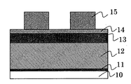
- プラズマエッチング装置を使用して被エッチング材の上に設けられたホトレジストおよび無機膜からなるマスクパターンを用いて前記被エッチング材をエッチングすることによって配線を形成するドライエッチング方法において、
前記ホトレジストをマスクパターンとして前記無機膜をエッチングし、
ハロゲン系ガスと、CF4、CHF3、SF6、NF3からなるフッ素含有ガスのうちの少なくとも一つのフッ素含有ガスと、の混合ガスを用いて前記エッチングされた無機膜を所望のマスクパターン寸法に縮小化させるまで前記被エッチング材をエッチングし、
前記所望の寸法に縮小化された無機膜をマスクパターンとして前記エッチングされた被エッチング材の残りをエッチングすることを特徴とするドライエッチング方法。 - プラズマエッチング装置を使用して被エッチング材の上に設けられた無機膜からなるマスクパターンを用いて前記被エッチング材をエッチングすることによって配線を形成するドライエッチング方法において、
ハロゲン系ガスと、CF 4 、CHF 3 、SF 6 、NF 3 からなるフッ素含有ガスのうちの少なくとも一つのフッ素含有ガスと、の混合ガスを用いて予めマスクパターンとしてエッチングされた無機膜を所望のマスクパターン寸法に縮小化させるまで前記被エッチング材をエッチングし、
前記所望の寸法に縮小化された無機膜をマスクパターンとして前記エッチングされた被エッチング材の残りをエッチングすることを特徴とするドライエッチング方法。 - 請求項1に記載のドライエッチング方法において、
前記ホトレジストをマスクパターンとして前記無機膜をエッチングする前に、O 2 ガスを用いて前記ホトレジストを所望のマスクパターン寸法に縮小化させることを特徴とするドライエッチング方法。 - 請求項1または2記載のドライエッチング方法において、
前記ハロゲン系ガスは、Cl 2 ガスであり、前記フッ素含有ガスの流量は、前記混合ガスの40〜90%の比率のガス流量であることを特徴とするドライエッチング方法。 - 請求項1または2記載のドライエッチング方法において、
前記ハロゲン系ガスは、HBrガスであり、前記フッ素含有ガスの流量は、前記混合ガスの40〜90%の比率のガス流量であることを特徴とするドライエッチング方法。
Priority Applications (5)
| Application Number | Priority Date | Filing Date | Title |
|---|---|---|---|
| JP2006054914A JP4865361B2 (ja) | 2006-03-01 | 2006-03-01 | ドライエッチング方法 |
| US11/505,292 US20070207618A1 (en) | 2006-03-01 | 2006-08-17 | Dry etching method |
| KR1020060078748A KR100894300B1 (ko) | 2006-03-01 | 2006-08-21 | 드라이에칭방법 |
| TW095131155A TW200735208A (en) | 2006-03-01 | 2006-08-24 | Dry etching method |
| US12/435,787 US8143175B2 (en) | 2006-03-01 | 2009-05-05 | Dry etching method |
Applications Claiming Priority (1)
| Application Number | Priority Date | Filing Date | Title |
|---|---|---|---|
| JP2006054914A JP4865361B2 (ja) | 2006-03-01 | 2006-03-01 | ドライエッチング方法 |
Publications (3)
| Publication Number | Publication Date |
|---|---|
| JP2007234870A JP2007234870A (ja) | 2007-09-13 |
| JP2007234870A5 JP2007234870A5 (ja) | 2009-02-19 |
| JP4865361B2 true JP4865361B2 (ja) | 2012-02-01 |
Family
ID=38471971
Family Applications (1)
| Application Number | Title | Priority Date | Filing Date |
|---|---|---|---|
| JP2006054914A Expired - Fee Related JP4865361B2 (ja) | 2006-03-01 | 2006-03-01 | ドライエッチング方法 |
Country Status (4)
| Country | Link |
|---|---|
| US (2) | US20070207618A1 (ja) |
| JP (1) | JP4865361B2 (ja) |
| KR (1) | KR100894300B1 (ja) |
| TW (1) | TW200735208A (ja) |
Families Citing this family (3)
| Publication number | Priority date | Publication date | Assignee | Title |
|---|---|---|---|---|
| JP2013258244A (ja) * | 2012-06-12 | 2013-12-26 | Tokyo Electron Ltd | エッチング方法及びプラズマ処理装置 |
| JP2014003085A (ja) * | 2012-06-15 | 2014-01-09 | Tokyo Electron Ltd | プラズマエッチング方法及びプラズマ処理装置 |
| CN104425228B (zh) * | 2013-08-28 | 2017-06-16 | 中芯国际集成电路制造(上海)有限公司 | 多晶硅栅极的形成方法 |
Family Cites Families (20)
| Publication number | Priority date | Publication date | Assignee | Title |
|---|---|---|---|---|
| JPS56100421A (en) * | 1980-01-17 | 1981-08-12 | Toshiba Corp | Plasma etching method |
| JPS56144542A (en) * | 1980-03-17 | 1981-11-10 | Ibm | Method of selectively reactively ion etching polycrystalline silicon for monocrsytalline silicon |
| EP0338102B1 (de) | 1988-04-19 | 1993-03-10 | International Business Machines Corporation | Verfahren zur Herstellung von integrierten Halbleiterstrukturen welche Feldeffekttransistoren mit Kanallängen im Submikrometerbereich enthalten |
| JPH07263415A (ja) | 1994-03-18 | 1995-10-13 | Fujitsu Ltd | 半導体装置の製造方法 |
| JP3438313B2 (ja) * | 1994-05-12 | 2003-08-18 | 富士通株式会社 | パターン形成方法 |
| KR100434133B1 (ko) | 1995-07-14 | 2004-08-09 | 텍사스 인스트루먼츠 인코포레이티드 | 중간층리쏘그래피 |
| JP2935346B2 (ja) * | 1996-07-30 | 1999-08-16 | 日本電気株式会社 | 半導体装置およびその製造方法 |
| US5818110A (en) * | 1996-11-22 | 1998-10-06 | International Business Machines Corporation | Integrated circuit chip wiring structure with crossover capability and method of manufacturing the same |
| KR100291585B1 (ko) | 1997-07-25 | 2001-11-30 | 윤종용 | 반도체장치의금속막식각방법 |
| KR20010003257A (ko) | 1999-06-22 | 2001-01-15 | 김영환 | 반도체소자의 제조방법 |
| JP2001035808A (ja) * | 1999-07-22 | 2001-02-09 | Semiconductor Energy Lab Co Ltd | 配線およびその作製方法、この配線を備えた半導体装置、ドライエッチング方法 |
| TW452971B (en) | 1999-12-28 | 2001-09-01 | Promos Technologies Inc | Manufacturing method of bottle-shaped deep trench |
| KR20010083476A (ko) | 2000-02-15 | 2001-09-01 | 박종섭 | 미세패턴 형성방법 |
| JP2002151470A (ja) * | 2000-11-09 | 2002-05-24 | Mitsubishi Electric Corp | ハードマスクの形成方法および半導体装置の製造方法 |
| JP2002343798A (ja) * | 2001-05-18 | 2002-11-29 | Mitsubishi Electric Corp | 配線層のドライエッチング方法、半導体装置の製造方法および該方法によって得られた半導体装置 |
| JP4257051B2 (ja) * | 2001-08-10 | 2009-04-22 | 株式会社ルネサステクノロジ | 半導体集積回路装置の製造方法 |
| JP2003163349A (ja) * | 2001-11-28 | 2003-06-06 | Mitsubishi Electric Corp | 半導体装置の製造方法 |
| US6900139B1 (en) | 2002-04-30 | 2005-05-31 | Advanced Micro Devices, Inc. | Method for photoresist trim endpoint detection |
| US6762130B2 (en) | 2002-05-31 | 2004-07-13 | Texas Instruments Incorporated | Method of photolithographically forming extremely narrow transistor gate elements |
| KR200291154Y1 (ko) * | 2002-07-09 | 2002-10-11 | 박성준 | 전기ㆍ전자기기의 전선 정리용 기구 |
-
2006
- 2006-03-01 JP JP2006054914A patent/JP4865361B2/ja not_active Expired - Fee Related
- 2006-08-17 US US11/505,292 patent/US20070207618A1/en not_active Abandoned
- 2006-08-21 KR KR1020060078748A patent/KR100894300B1/ko not_active IP Right Cessation
- 2006-08-24 TW TW095131155A patent/TW200735208A/zh not_active IP Right Cessation
-
2009
- 2009-05-05 US US12/435,787 patent/US8143175B2/en not_active Expired - Fee Related
Also Published As
| Publication number | Publication date |
|---|---|
| KR20070090063A (ko) | 2007-09-05 |
| US8143175B2 (en) | 2012-03-27 |
| KR100894300B1 (ko) | 2009-04-24 |
| TW200735208A (en) | 2007-09-16 |
| US20070207618A1 (en) | 2007-09-06 |
| JP2007234870A (ja) | 2007-09-13 |
| US20090280651A1 (en) | 2009-11-12 |
| TWI334174B (ja) | 2010-12-01 |
Similar Documents
| Publication | Publication Date | Title |
|---|---|---|
| JP4579611B2 (ja) | ドライエッチング方法 | |
| US8394722B2 (en) | Bi-layer, tri-layer mask CD control | |
| US20050277289A1 (en) | Line edge roughness reduction for trench etch | |
| KR20160044545A (ko) | 하드마스크를 측면으로 트리밍하기 위한 방법 | |
| JP3165047B2 (ja) | ポリサイド膜のドライエッチング方法 | |
| JP2004519838A (ja) | 窒化チタンをエッチングする方法 | |
| US20080254637A1 (en) | Methods for removing photoresist defects and a source gas for same | |
| JP2014107520A (ja) | プラズマエッチング方法 | |
| JP2010016213A (ja) | プラズマエッチング方法、制御プログラム及びコンピュータ記憶媒体 | |
| US9966312B2 (en) | Method for etching a silicon-containing substrate | |
| JP4865361B2 (ja) | ドライエッチング方法 | |
| JP5248063B2 (ja) | 半導体素子加工方法 | |
| JP5297615B2 (ja) | ドライエッチング方法 | |
| JP3353532B2 (ja) | トレンチエッチング方法 | |
| JPH08321484A (ja) | 半導体装置の製造方法 | |
| JP2004259927A (ja) | ドライエッチング方法 | |
| JP6040314B2 (ja) | プラズマ処理方法 | |
| JP4778715B2 (ja) | 半導体の製造方法 | |
| JP5815459B2 (ja) | プラズマエッチング方法 | |
| JP4368244B2 (ja) | ドライエッチング方法 | |
| JP2010062212A (ja) | 半導体装置の製造方法 | |
| JPH0677175A (ja) | 酸化シリコン上の窒化シリコンのエッチング方法 | |
| JP2005310944A (ja) | ドライエッチング方法 |
Legal Events
| Date | Code | Title | Description |
|---|---|---|---|
| A521 | Written amendment |
Free format text: JAPANESE INTERMEDIATE CODE: A523 Effective date: 20081224 |
|
| A621 | Written request for application examination |
Free format text: JAPANESE INTERMEDIATE CODE: A621 Effective date: 20081224 |
|
| A977 | Report on retrieval |
Free format text: JAPANESE INTERMEDIATE CODE: A971007 Effective date: 20090601 |
|
| A131 | Notification of reasons for refusal |
Free format text: JAPANESE INTERMEDIATE CODE: A131 Effective date: 20110830 |
|
| A521 | Written amendment |
Free format text: JAPANESE INTERMEDIATE CODE: A523 Effective date: 20111012 |
|
| TRDD | Decision of grant or rejection written | ||
| A01 | Written decision to grant a patent or to grant a registration (utility model) |
Free format text: JAPANESE INTERMEDIATE CODE: A01 Effective date: 20111108 |
|
| A01 | Written decision to grant a patent or to grant a registration (utility model) |
Free format text: JAPANESE INTERMEDIATE CODE: A01 |
|
| A61 | First payment of annual fees (during grant procedure) |
Free format text: JAPANESE INTERMEDIATE CODE: A61 Effective date: 20111110 |
|
| FPAY | Renewal fee payment (event date is renewal date of database) |
Free format text: PAYMENT UNTIL: 20141118 Year of fee payment: 3 |
|
| R150 | Certificate of patent or registration of utility model |
Free format text: JAPANESE INTERMEDIATE CODE: R150 |
|
| LAPS | Cancellation because of no payment of annual fees |