JP4865361B2 - Dry etching method - Google Patents
Dry etching method Download PDFInfo
- Publication number
- JP4865361B2 JP4865361B2 JP2006054914A JP2006054914A JP4865361B2 JP 4865361 B2 JP4865361 B2 JP 4865361B2 JP 2006054914 A JP2006054914 A JP 2006054914A JP 2006054914 A JP2006054914 A JP 2006054914A JP 4865361 B2 JP4865361 B2 JP 4865361B2
- Authority
- JP
- Japan
- Prior art keywords
- gas
- etched
- etching
- dry etching
- mask pattern
- Prior art date
- Legal status (The legal status is an assumption and is not a legal conclusion. Google has not performed a legal analysis and makes no representation as to the accuracy of the status listed.)
- Expired - Fee Related
Links
- 238000000034 method Methods 0.000 title claims description 45
- 238000001312 dry etching Methods 0.000 title claims description 20
- 238000005530 etching Methods 0.000 claims description 44
- 229920002120 photoresistant polymer Polymers 0.000 claims description 32
- 239000000463 material Substances 0.000 claims description 27
- 238000001020 plasma etching Methods 0.000 claims description 15
- YCKRFDGAMUMZLT-UHFFFAOYSA-N Fluorine atom Chemical compound [F] YCKRFDGAMUMZLT-UHFFFAOYSA-N 0.000 claims description 10
- 229910052731 fluorine Inorganic materials 0.000 claims description 10
- 239000011737 fluorine Substances 0.000 claims description 10
- 229910052736 halogen Inorganic materials 0.000 claims description 5
- 150000002367 halogens Chemical class 0.000 claims description 5
- 229910021420 polycrystalline silicon Inorganic materials 0.000 description 22
- 229920005591 polysilicon Polymers 0.000 description 22
- 229910052814 silicon oxide Inorganic materials 0.000 description 14
- 239000004065 semiconductor Substances 0.000 description 11
- 239000000758 substrate Substances 0.000 description 8
- 238000005452 bending Methods 0.000 description 5
- XUIMIQQOPSSXEZ-UHFFFAOYSA-N Silicon Chemical compound [Si] XUIMIQQOPSSXEZ-UHFFFAOYSA-N 0.000 description 4
- 229910052710 silicon Inorganic materials 0.000 description 4
- 239000010703 silicon Substances 0.000 description 4
- BSYNRYMUTXBXSQ-UHFFFAOYSA-N Aspirin Chemical compound CC(=O)OC1=CC=CC=C1C(O)=O BSYNRYMUTXBXSQ-UHFFFAOYSA-N 0.000 description 2
- 230000015572 biosynthetic process Effects 0.000 description 2
- 230000007547 defect Effects 0.000 description 2
- 238000009616 inductively coupled plasma Methods 0.000 description 2
- 238000004519 manufacturing process Methods 0.000 description 2
- 239000012528 membrane Substances 0.000 description 2
- 239000010453 quartz Substances 0.000 description 2
- 238000011946 reduction process Methods 0.000 description 2
- VYPSYNLAJGMNEJ-UHFFFAOYSA-N silicon dioxide Inorganic materials O=[Si]=O VYPSYNLAJGMNEJ-UHFFFAOYSA-N 0.000 description 2
- 238000005549 size reduction Methods 0.000 description 2
- 229910004541 SiN Inorganic materials 0.000 description 1
- 229910004298 SiO 2 Inorganic materials 0.000 description 1
- 230000001133 acceleration Effects 0.000 description 1
- 238000007796 conventional method Methods 0.000 description 1
- 238000010586 diagram Methods 0.000 description 1
- 230000000694 effects Effects 0.000 description 1
- 230000005284 excitation Effects 0.000 description 1
- 230000010354 integration Effects 0.000 description 1
- 150000002500 ions Chemical class 0.000 description 1
- 238000000206 photolithography Methods 0.000 description 1
- 238000003672 processing method Methods 0.000 description 1
- WNUPENMBHHEARK-UHFFFAOYSA-N silicon tungsten Chemical compound [Si].[W] WNUPENMBHHEARK-UHFFFAOYSA-N 0.000 description 1
- 238000001179 sorption measurement Methods 0.000 description 1
Images


Classifications
-
- H—ELECTRICITY
- H01—ELECTRIC ELEMENTS
- H01L—SEMICONDUCTOR DEVICES NOT COVERED BY CLASS H10
- H01L21/00—Processes or apparatus adapted for the manufacture or treatment of semiconductor or solid state devices or of parts thereof
- H01L21/02—Manufacture or treatment of semiconductor devices or of parts thereof
- H01L21/04—Manufacture or treatment of semiconductor devices or of parts thereof the devices having potential barriers, e.g. a PN junction, depletion layer or carrier concentration layer
- H01L21/18—Manufacture or treatment of semiconductor devices or of parts thereof the devices having potential barriers, e.g. a PN junction, depletion layer or carrier concentration layer the devices having semiconductor bodies comprising elements of Group IV of the Periodic Table or AIIIBV compounds with or without impurities, e.g. doping materials
- H01L21/30—Treatment of semiconductor bodies using processes or apparatus not provided for in groups H01L21/20 - H01L21/26
- H01L21/31—Treatment of semiconductor bodies using processes or apparatus not provided for in groups H01L21/20 - H01L21/26 to form insulating layers thereon, e.g. for masking or by using photolithographic techniques; After treatment of these layers; Selection of materials for these layers
- H01L21/3205—Deposition of non-insulating-, e.g. conductive- or resistive-, layers on insulating layers; After-treatment of these layers
- H01L21/321—After treatment
- H01L21/3213—Physical or chemical etching of the layers, e.g. to produce a patterned layer from a pre-deposited extensive layer
- H01L21/32139—Physical or chemical etching of the layers, e.g. to produce a patterned layer from a pre-deposited extensive layer using masks
-
- H—ELECTRICITY
- H01—ELECTRIC ELEMENTS
- H01L—SEMICONDUCTOR DEVICES NOT COVERED BY CLASS H10
- H01L21/00—Processes or apparatus adapted for the manufacture or treatment of semiconductor or solid state devices or of parts thereof
- H01L21/02—Manufacture or treatment of semiconductor devices or of parts thereof
- H01L21/04—Manufacture or treatment of semiconductor devices or of parts thereof the devices having potential barriers, e.g. a PN junction, depletion layer or carrier concentration layer
- H01L21/18—Manufacture or treatment of semiconductor devices or of parts thereof the devices having potential barriers, e.g. a PN junction, depletion layer or carrier concentration layer the devices having semiconductor bodies comprising elements of Group IV of the Periodic Table or AIIIBV compounds with or without impurities, e.g. doping materials
- H01L21/30—Treatment of semiconductor bodies using processes or apparatus not provided for in groups H01L21/20 - H01L21/26
- H01L21/302—Treatment of semiconductor bodies using processes or apparatus not provided for in groups H01L21/20 - H01L21/26 to change their surface-physical characteristics or shape, e.g. etching, polishing, cutting
- H01L21/306—Chemical or electrical treatment, e.g. electrolytic etching
- H01L21/3065—Plasma etching; Reactive-ion etching
-
- H—ELECTRICITY
- H01—ELECTRIC ELEMENTS
- H01L—SEMICONDUCTOR DEVICES NOT COVERED BY CLASS H10
- H01L21/00—Processes or apparatus adapted for the manufacture or treatment of semiconductor or solid state devices or of parts thereof
- H01L21/02—Manufacture or treatment of semiconductor devices or of parts thereof
- H01L21/027—Making masks on semiconductor bodies for further photolithographic processing not provided for in group H01L21/18 or H01L21/34
- H01L21/033—Making masks on semiconductor bodies for further photolithographic processing not provided for in group H01L21/18 or H01L21/34 comprising inorganic layers
- H01L21/0334—Making masks on semiconductor bodies for further photolithographic processing not provided for in group H01L21/18 or H01L21/34 comprising inorganic layers characterised by their size, orientation, disposition, behaviour, shape, in horizontal or vertical plane
- H01L21/0338—Process specially adapted to improve the resolution of the mask
-
- H—ELECTRICITY
- H01—ELECTRIC ELEMENTS
- H01L—SEMICONDUCTOR DEVICES NOT COVERED BY CLASS H10
- H01L21/00—Processes or apparatus adapted for the manufacture or treatment of semiconductor or solid state devices or of parts thereof
- H01L21/02—Manufacture or treatment of semiconductor devices or of parts thereof
- H01L21/04—Manufacture or treatment of semiconductor devices or of parts thereof the devices having potential barriers, e.g. a PN junction, depletion layer or carrier concentration layer
- H01L21/18—Manufacture or treatment of semiconductor devices or of parts thereof the devices having potential barriers, e.g. a PN junction, depletion layer or carrier concentration layer the devices having semiconductor bodies comprising elements of Group IV of the Periodic Table or AIIIBV compounds with or without impurities, e.g. doping materials
- H01L21/28—Manufacture of electrodes on semiconductor bodies using processes or apparatus not provided for in groups H01L21/20 - H01L21/268
- H01L21/28008—Making conductor-insulator-semiconductor electrodes
- H01L21/28017—Making conductor-insulator-semiconductor electrodes the insulator being formed after the semiconductor body, the semiconductor being silicon
- H01L21/28026—Making conductor-insulator-semiconductor electrodes the insulator being formed after the semiconductor body, the semiconductor being silicon characterised by the conductor
- H01L21/28123—Lithography-related aspects, e.g. sub-lithography lengths; Isolation-related aspects, e.g. to solve problems arising at the crossing with the side of the device isolation; Planarisation aspects
-
- H—ELECTRICITY
- H01—ELECTRIC ELEMENTS
- H01L—SEMICONDUCTOR DEVICES NOT COVERED BY CLASS H10
- H01L21/00—Processes or apparatus adapted for the manufacture or treatment of semiconductor or solid state devices or of parts thereof
- H01L21/02—Manufacture or treatment of semiconductor devices or of parts thereof
- H01L21/04—Manufacture or treatment of semiconductor devices or of parts thereof the devices having potential barriers, e.g. a PN junction, depletion layer or carrier concentration layer
- H01L21/18—Manufacture or treatment of semiconductor devices or of parts thereof the devices having potential barriers, e.g. a PN junction, depletion layer or carrier concentration layer the devices having semiconductor bodies comprising elements of Group IV of the Periodic Table or AIIIBV compounds with or without impurities, e.g. doping materials
- H01L21/30—Treatment of semiconductor bodies using processes or apparatus not provided for in groups H01L21/20 - H01L21/26
- H01L21/31—Treatment of semiconductor bodies using processes or apparatus not provided for in groups H01L21/20 - H01L21/26 to form insulating layers thereon, e.g. for masking or by using photolithographic techniques; After treatment of these layers; Selection of materials for these layers
- H01L21/3105—After-treatment
- H01L21/311—Etching the insulating layers by chemical or physical means
- H01L21/31105—Etching inorganic layers
- H01L21/31111—Etching inorganic layers by chemical means
- H01L21/31116—Etching inorganic layers by chemical means by dry-etching
-
- H—ELECTRICITY
- H01—ELECTRIC ELEMENTS
- H01L—SEMICONDUCTOR DEVICES NOT COVERED BY CLASS H10
- H01L21/00—Processes or apparatus adapted for the manufacture or treatment of semiconductor or solid state devices or of parts thereof
- H01L21/02—Manufacture or treatment of semiconductor devices or of parts thereof
- H01L21/04—Manufacture or treatment of semiconductor devices or of parts thereof the devices having potential barriers, e.g. a PN junction, depletion layer or carrier concentration layer
- H01L21/18—Manufacture or treatment of semiconductor devices or of parts thereof the devices having potential barriers, e.g. a PN junction, depletion layer or carrier concentration layer the devices having semiconductor bodies comprising elements of Group IV of the Periodic Table or AIIIBV compounds with or without impurities, e.g. doping materials
- H01L21/30—Treatment of semiconductor bodies using processes or apparatus not provided for in groups H01L21/20 - H01L21/26
- H01L21/31—Treatment of semiconductor bodies using processes or apparatus not provided for in groups H01L21/20 - H01L21/26 to form insulating layers thereon, e.g. for masking or by using photolithographic techniques; After treatment of these layers; Selection of materials for these layers
- H01L21/3205—Deposition of non-insulating-, e.g. conductive- or resistive-, layers on insulating layers; After-treatment of these layers
- H01L21/321—After treatment
- H01L21/3213—Physical or chemical etching of the layers, e.g. to produce a patterned layer from a pre-deposited extensive layer
- H01L21/32133—Physical or chemical etching of the layers, e.g. to produce a patterned layer from a pre-deposited extensive layer by chemical means only
- H01L21/32135—Physical or chemical etching of the layers, e.g. to produce a patterned layer from a pre-deposited extensive layer by chemical means only by vapour etching only
- H01L21/32136—Physical or chemical etching of the layers, e.g. to produce a patterned layer from a pre-deposited extensive layer by chemical means only by vapour etching only using plasmas
- H01L21/32137—Physical or chemical etching of the layers, e.g. to produce a patterned layer from a pre-deposited extensive layer by chemical means only by vapour etching only using plasmas of silicon-containing layers
Landscapes
- Engineering & Computer Science (AREA)
- Physics & Mathematics (AREA)
- Power Engineering (AREA)
- Condensed Matter Physics & Semiconductors (AREA)
- General Physics & Mathematics (AREA)
- Manufacturing & Machinery (AREA)
- Computer Hardware Design (AREA)
- Microelectronics & Electronic Packaging (AREA)
- Chemical & Material Sciences (AREA)
- Inorganic Chemistry (AREA)
- Chemical Kinetics & Catalysis (AREA)
- General Chemical & Material Sciences (AREA)
- Plasma & Fusion (AREA)
- Drying Of Semiconductors (AREA)
- Internal Circuitry In Semiconductor Integrated Circuit Devices (AREA)
- Electrodes Of Semiconductors (AREA)
Description
本発明は、半導体デバイスのエッチング方法に関する。さらに詳細には、半導体基板に設けた配線層である被エッチング材を加工しながら加工寸法を縮小化させることにより、パターン欠陥を発生させずに配線寸法の縮小化を行うドライエッチング方法に関する。 The present invention relates to a method for etching a semiconductor device. More specifically, the present invention relates to a dry etching method for reducing a wiring dimension without generating a pattern defect by reducing a processing dimension while processing a material to be etched which is a wiring layer provided on a semiconductor substrate.
近年、半導体デバイスの処理速度の高速化に伴なう高集積化の進展により、ゲート材等の加工技術においても微細化加工が求められている。ドライエッチングの分野では、一般的にパターンの微細化を行うために、被エッチング材を加工する前に、マスクとなるホトレジストパターンをドライエッチングにより縮小化させることで、被エッチング材の加工寸法を縮小化する方法が行われてきた。 In recent years, with the progress of high integration accompanying the increase in the processing speed of semiconductor devices, miniaturization processing is also required in processing techniques for gate materials and the like. In the field of dry etching, in general, in order to make the pattern finer, before processing the material to be etched, the photoresist pattern to be a mask is reduced by dry etching to reduce the processing size of the material to be etched. A method has been carried out.
さらに微細化が進むと、ホトレジストマスクの素材を、従来よりも高精度に微細パターンが形成できるArFレーザを用いて露光するArFレジストが採用されるようになった。しかし、ArFレジストは従来のマスク材と比べると厚く膜付けできず、しかもエッチング速度が速いことからエッチングに対して弱いという性質を有している。このため、ArFレジストは、被エッチング材を加工する間にマスクが無くなり、高精度な被エッチング材の微細配線加工ができないという問題を有している。この問題を解決するために、ホトレジストマスクと被エッチング材との間にSiON、SiN、SiO等の無機膜層を設け、縮小化したホトレジストマスクのパターンを元にドライエッチングにより無機膜層を加工し、エッチング速度の遅い無機膜マスクを形成することで、安定して被エッチング材の加工が行えるようにしている(例えば、特許文献1参照)。
しかし、ドライエッチングによるホトレジストパターン寸法の縮小化方法では、無機膜層の加工に必要なホトレジストマスク量を確保することが必要であり、加工寸法の縮小量に限界が生じるという問題がある。 However, in the method of reducing the photoresist pattern dimension by dry etching, it is necessary to secure a photoresist mask amount necessary for processing the inorganic film layer, and there is a problem that a reduction amount of the processing dimension is limited.
本発明は、被エッチング材の加工中に加工寸法を縮小化することが可能となり、マスク欠損による被エッチング材の断線や曲がり等の問題を発生させずに、微細加工を行うことができるドライエッチング方法を提供することを目的とする。 The present invention makes it possible to reduce the processing dimension during processing of the material to be etched, and dry etching that can perform fine processing without causing problems such as disconnection or bending of the material to be etched due to mask defects. It aims to provide a method.
この課題は、パターンニングされたホトレジストをマスクとし、ドライエッチングにより無機膜層を加工して無機膜マスクの形成を行った後、被エッチング材のエッチング過程で、無機膜マスクと被エッチング材とを同時に縮小化させることにより達成できる。 The problem is that after the inorganic film layer is formed by processing the inorganic film layer by dry etching using the patterned photoresist as a mask, the inorganic film mask and the material to be etched are removed in the etching process of the material to be etched. This can be achieved by reducing the size simultaneously.
この加工方法では、無機膜マスクを形成した後にこの無機膜マスクのパターン寸法の縮小化を行うので、ホトレジストマスク倒れ等の問題が発生しない。 In this processing method, since the pattern dimension of the inorganic film mask is reduced after the inorganic film mask is formed, problems such as photoresist mask collapse do not occur.
また、従来から行っているドライエッチングによるホトレジストマスク寸法の縮小化を併用する場合でも、過剰なホトレジストマスクの縮小化を行う必要が無く、このためパターン縮小による倒れや配線層の断線等の問題が発生しない。 In addition, even when the conventional photoresist mask size reduction by dry etching is used together, it is not necessary to reduce the photoresist mask excessively, which causes problems such as collapse due to pattern reduction and disconnection of the wiring layer. Does not occur.
上記の方法により、本発明によれば、加工寸法の縮小化に伴う被エッチング材の配線の断線や曲がりを発生させること無く、加工寸法を大幅に縮小させることができ、微細な配線加工を行うことができる。 By the above method, according to the present invention, the processing dimension can be greatly reduced without causing disconnection or bending of the wiring of the material to be etched due to the reduction of the processing dimension, and fine wiring processing is performed. be able to.
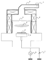
以下、本発明によるプラズマエッチング方法について説明する。図1は、本発明にかかるドライエッチング方法が適用されるプラズマエッチング装置を示す。このプラズマエッチング装置は、プラズマ生成手段にマイクロ波と磁界を利用したマイクロ波プラズマエッチング装置の例である。マイクロ波は、マグネトロン1で発振され,導波管2を経て石英板3を通過して真空容器へ入射される。真空容器の周りにはソレノイドコイル4が設けてあり、これより発生する磁界と入射してくるマイクロ波により、電子サイクロトロン共鳴(ECR: Electron Cyclotron Resonance)を起こす。これによりプロセスガスは、効率良く高密度にプラズマ5化される。処理ウエハ6は、静電吸着電源7で試料台8に直流電圧を印加することで、静電吸着力により電極に固定される。また,電極には高周波電源9が接続してあり,高周波電力(RFバイアス)を印加して,プラズマ中のイオンにウエハに対して垂直方向の加速電位を与える。エッチング後のガスは装置下部に設けられた排気口から、ターボポンプ・ドライポンプ(図省略)により排気される。
The plasma etching method according to the present invention will be described below. FIG. 1 shows a plasma etching apparatus to which a dry etching method according to the present invention is applied. This plasma etching apparatus is an example of a microwave plasma etching apparatus that uses a microwave and a magnetic field as plasma generation means. The microwave is oscillated by the magnetron 1 and passes through the quartz plate 3 through the waveguide 2 and enters the vacuum vessel. A solenoid coil 4 is provided around the vacuum vessel, and an electron cyclotron resonance (ECR) is generated by a magnetic field generated therefrom and incident microwaves. As a result, the process gas is efficiently converted into plasma 5 at a high density. The processing wafer 6 is fixed to the electrode by electrostatic attraction force by applying a DC voltage to the
なお、プラズマエッチング処理装置としては、マイクロ波プラズマエッチング装置、誘導結合型プラズマエッチング装置、ヘリコン波プラズマエッチング装置、2周波励起平行平板型プラズマエッチング装置などが採用される。 As the plasma etching apparatus, a microwave plasma etching apparatus, an inductively coupled plasma etching apparatus, a helicon wave plasma etching apparatus, a two-frequency excitation parallel plate plasma etching apparatus, or the like is employed.
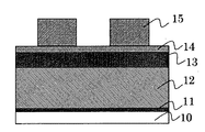
図2は、図1のプラズマエッチング装置を用いた半導体装置の製造方法を示す図である。図2(A)は本実施例で使用する試料の構造を、図2(B)はホトレジストマスクの加工寸法の縮小工程を、図2(C)はSiON膜、SiN膜のマスク形成工程を、図2(D)はマスクおよびポリシリコン膜の加工および加工寸法の縮小工程を、図2(E)はポリシリコン膜の加工工程を示す。 FIG. 2 is a diagram illustrating a method of manufacturing a semiconductor device using the plasma etching apparatus of FIG. 2A shows the structure of the sample used in this example, FIG. 2B shows the process of reducing the processing size of the photoresist mask, FIG. 2C shows the mask forming process of the SiON film and SiN film, FIG. 2D shows a mask and polysilicon film processing and a process size reduction process, and FIG. 2E shows a polysilicon film processing process.
本発明の一実施例で使用した試料の構造の例を、図2(A)に示す。直径12インチのシリコン基板10の上にゲート酸化膜(2nm)11、ポリシリコン膜(膜厚100nm)12、SiN膜(50nm)13、SiON膜(25nm)14、ホトレジスト(250nm)15を順に形成し、フォトリソグラフィ技術等よってマスクパターンを形成する。
An example of the structure of the sample used in one example of the present invention is shown in FIG. A gate oxide film (2 nm) 11, a polysilicon film (film thickness 100 nm) 12, an SiN film (50 nm) 13, an SiON film (25 nm) 14, and a photoresist (250 nm) 15 are formed in this order on a
図2(B)は、従来から行われているホトレジストマスクの加工寸法の縮小工程であり、例えば、ArガスにO2ガスを添加した混合ガスを用い、処理圧力を0.2Paに設定し、マイクロ波を600Wとして生成したプラズマでエッチングを行う。O2ガス流量はホトレジストの縮小速度を律しており、1.5nm/sec程度の縮小速度とするため10%程度添加した。O2ガスの添加量を増加させると縮小速度は上昇する。本実施例では、初期ホトレジストパターン寸法が100nmであるパターンに対して43秒処理を行い、ホトレジストパターン寸法を35nmまで細らせた。 FIG. 2B is a conventional process for reducing the processing dimension of a photoresist mask. For example, using a mixed gas obtained by adding O 2 gas to Ar gas, the processing pressure is set to 0.2 Pa, Etching is performed with plasma generated with a microwave of 600 W. The O 2 gas flow rate regulates the reduction rate of the photoresist, and about 10% was added to obtain a reduction rate of about 1.5 nm / sec. Increasing the amount of O 2 gas added increases the reduction rate. In this example, a pattern having an initial photoresist pattern dimension of 100 nm was processed for 43 seconds to reduce the photoresist pattern dimension to 35 nm.
図2(C)に示すマスク形成工程ではホトレジスト15をマスクとして、SiON膜14およびSiN膜13をエッチングする。エッチング処理中は、EPD(End Point Detector)等のエッチングモニターで、ポリシリコン膜12との界面を検出しながらエッチング処理を行う。処理条件として、例えば、CF4ガスとCHF3ガス1:1の混合ガスを用い、処理圧力を0.8Paとし、マイクロ波900Wで生成したプラズマにRFバイアス100Wを印加しエッチングする。ポリシリコン膜12の表面を検出した時点でSiN膜13のエッチングを終了する。
In the mask formation step shown in FIG. 2C, the SiON
図2(D)に示すポリシリコン膜の加工寸法の縮小工程は、本発明の特徴とする工程であり、図2(C)により形成されたSiON膜14およびSiN膜13のパターンをマスクとして深さ方向のエッチングを進行させながら、横方向のエッチングを同時に行うことでパターン寸法の縮小化を行う。Cl2と共にCF4を用いることで、ポリシリコン膜12のエッチングと同時に、マスク材もエッチングすることができる。処理条件として例えば、Cl2ガスとCF4ガス1:3の混合ガスを用い、処理圧力を0.2Paとし、マイクロ波900Wで生成したプラズマにRFバイアス30Wを印加し深さ方向および横方向をエッチングする。
The process for reducing the processing dimension of the polysilicon film shown in FIG. 2D is a process characterized by the present invention. The process is performed by using the pattern of the SiON
ここで、ポリシリコンの横方向のエッチング量は、図3(A)に示すように、RFバイアスの印加量に依存することが分かり、この実施例では、処理条件は深さ方向に対する横方向の縮小比率を0.32程度に最適化を行った。本実施例では、ポリシリコン膜12の厚100nmに対して半分の50nm程度をこの処理条件で処理を行い、前記ホトレジスト14およびSiON膜14ならびにSiN膜13の加工寸法縮小工程により35nmまで縮小化されたパターンを、さらに16nmの縮小化を行い19nmのパターン寸法を形成した。この処理工程によって、ホトレジスト14は全てエッチングされ、これ以降SiON膜14およびSiN膜13がマスクとして使用される。この工程は、ホトレジスト14がなくなるまでもしくは所望の(例えば、19nm)マスク幅となるまでは、等方性エッチを続けることができる。図3(A)における、縮小量とは、図3(B)に示すようにマスクの幅の初期寸法Aからエッチング後の寸法Bを差引いた値であり、縮小率は、この縮小量をポリシリコン膜のエッチング深さで除した値である。
Here, it can be seen that the etching amount in the lateral direction of the polysilicon depends on the application amount of the RF bias as shown in FIG. 3A. In this embodiment, the processing condition is in the lateral direction with respect to the depth direction. The reduction ratio was optimized to about 0.32. In this embodiment, about 50 nm, which is half of the thickness of the
図2(E)に示すポリシリコン膜12の加工工程は、前工程にて縮小化されたポリシリコンの加工寸法を維持しながら残りのポリシリコン膜のエッチングを行う。処理条件としては、例えば、HBrガスにO2ガスをHBrガス流量の4%程度添加した混合ガスを用い、処理圧力を0.4Paとし、マイクロ波900Wで生成したプラズマにRFバイアス30Wを印加してエッチングする。ここで使用するエッチング条件では、ポリシリコンの横方向のエッチングは起こらず、上層で形成された加工寸法を維持したままエッチング加工される。
In the processing step of the
これにより本実施例では、100nmの初期寸法を示すマスクパターンを用いて、被エッチング材に断線の発生や曲がり(サイドエッチング)の無い19nm幅のポリシリコン配線加工を実現することができた。 As a result, in this example, using a mask pattern having an initial dimension of 100 nm, it was possible to realize polysilicon wiring processing having a width of 19 nm without occurrence of disconnection or bending (side etching) in the material to be etched.
同様に、従来技術である図2(B)のホトレジスト15のパターン寸法の縮小化だけで、19nmのポリシリコンの加工を実現しようとすると、ホトレジストでの縮小化を80nm程度行う必要があり、ホトレジストパターンが倒れてしまい、ポリシリコン配線の断線や曲がり(サイドエッチング)等の問題が発生した。
Similarly, if the processing of 19 nm polysilicon is to be realized only by reducing the pattern dimension of the
従来技術により大幅なホトレジスト15のパターン寸法の縮小化を進めると、SiON膜14およびSiN膜13をエッチングするための十分なマスク量が保てなくなる。仮にマスク量を確保できた場合でも、ホトレジストパターンが薄膜化されることにより対プラズマ耐性が著しく低下し、パターン曲り等の問題が発生する。
If the pattern size of the
また、図2(D)で処理した処理条件(Cl2ガス:CF4ガス=1:3)は、本実施例の試料に合せて最適化された条件であり、CF4の添加量は形状制御の面から考えると40%〜90%が適当である。40%以下のCF4添加量ではフッ素による横方向のエッチングが進行しにくくなり縮小化が難しくなる。一方、90%以上のCF4添加量になるとフッ素による等方性エッチングが強くなりサイドエッチングが強くなって垂直形状が得られなくなる。図3に示す縮小速度制御方法すなわち前記処理条件の他に、Cl2ガスとCF4ガスに、O2ガスを添加すること、CHF3、SF6、NF3等のフッ素含有ガスを添加すること、もしくはCF4ガスに変えてCHF3、SF6、NF3等のフッ素含有ガスを使用することでも縮小速度を制御することができる。また同様に、Cl2ガスの代わりにHBrガス等のハロゲン系ガスを用いることでも、縮小速度を調整することができる。 Further, the processing conditions (Cl 2 gas: CF 4 gas = 1: 3) processed in FIG. 2D are conditions optimized for the sample of this example, and the amount of CF 4 added is the shape. From the viewpoint of control, 40% to 90% is appropriate. When the amount of CF 4 added is 40% or less, lateral etching by fluorine does not proceed easily, and it is difficult to reduce the size. On the other hand, when the amount of CF 4 added is 90% or more, isotropic etching with fluorine becomes strong, side etching becomes strong, and a vertical shape cannot be obtained. In addition to the reduction speed control method shown in FIG. 3, that is, the above processing conditions, adding O 2 gas to Cl 2 gas and CF 4 gas, adding fluorine-containing gas such as CHF 3 , SF 6 , NF 3, etc. Alternatively, the reduction rate can be controlled by using a fluorine-containing gas such as CHF 3 , SF 6 , or NF 3 instead of the CF 4 gas. Similarly, the reduction speed can be adjusted by using a halogen-based gas such as HBr gas instead of the Cl 2 gas.
本実施例は、半導体デバイスの試料について最適化を行ったプロセス条件であり、ポリシリコン膜12、SiN膜13、SiON膜14、ホトレジスト15のエッチング方法については、本実施例の条件に限られたものではない。
This embodiment is a process condition optimized for a semiconductor device sample, and the etching method of the
本発明は、ポリシリコンの配線加工工程について記載したが、それに限るものではなく、半導体デバイス製造工程において、ポリシリコン以外の材質の配線加工についても本発明の方法が適応可能であり、例えば、ポリシリコン膜12の上にタングステンシリサイド(WSi)膜を形成し、その上にSiN膜13およびSiON膜14ならびにホトレジスト15等を形成した場合の配線加工などにも応用することができる。加工する材料によって、縮小速度が違う為、材質に応じて使用するガスや処理条件の適性値を求めることが好ましい。
Although the present invention has been described with respect to a polysilicon wiring processing step, the present invention is not limited to this, and the method of the present invention can also be applied to wiring processing of materials other than polysilicon in a semiconductor device manufacturing process. The present invention can also be applied to wiring processing in the case where a tungsten silicide (WSi) film is formed on the
本試験では、ホトレジストマスクの試料を用いたが、SiNや、SiON、SiO2等の無機膜マスクを用いた試料、すなわち図2(D)のホトレジスト15が取り除かれた状態にされた試料についても、本発明の方法が適応可能である。
In this test, a sample of a photoresist mask was used. However, a sample using an inorganic film mask such as SiN, SiON, or SiO 2 , that is, a sample in which the
なお、本発明は、マイクロ波と磁場を用いたプラズマエッチング装置を使用したが、プラズマの生成方法の如何に関わらず適用可能であり、例えば、ヘリコン波プラズマエッチング装置、誘導結合型プラズマエッチング装置、容量結合型プラズマエッチング装置等によって実施しても同等の効果を得ることができる。 The present invention uses a plasma etching apparatus using a microwave and a magnetic field, but can be applied regardless of the plasma generation method. For example, a helicon wave plasma etching apparatus, an inductively coupled plasma etching apparatus, The same effect can be obtained even when implemented by a capacitively coupled plasma etching apparatus or the like.
1…マグネトロン、2…導波管、3…石英版、4…ソレノイドコイル、5…プラズマ、6…ウエハ、7…静電吸着電源、8…試料台、9…高周波電源、10…シリコン基板、11…ゲート酸化膜、12…ポリシリコン膜、13…SiN膜、14…SiON膜、15…ホトレジスト
DESCRIPTION OF SYMBOLS 1 ... Magnetron, 2 ... Waveguide, 3 ... Quartz plate, 4 ... Solenoid coil, 5 ... Plasma, 6 ... Wafer, 7 ... Electrostatic adsorption power supply, 8 ... Sample stand, 9 ... High frequency power supply, 10 ... Silicon substrate, DESCRIPTION OF
Claims (5)
前記ホトレジストをマスクパターンとして前記無機膜をエッチングし、
ハロゲン系ガスと、CF4、CHF3、SF6、NF3からなるフッ素含有ガスのうちの少なくとも一つのフッ素含有ガスと、の混合ガスを用いて前記エッチングされた無機膜を所望のマスクパターン寸法に縮小化させるまで前記被エッチング材をエッチングし、
前記所望の寸法に縮小化された無機膜をマスクパターンとして前記エッチングされた被エッチング材の残りをエッチングすることを特徴とするドライエッチング方法。 In a dry etching method for forming a wiring by etching the material to be etched using a mask pattern made of a photoresist and an inorganic film provided on the material to be etched using a plasma etching apparatus,
Etching the inorganic film using the photoresist as a mask pattern,
A halogen-based gas, CF 4, CHF 3, SF 6, a desired mask pattern at least one and a fluorine-containing gas, mixed have use a gas the etched inorganic film of NF 3 fluorine containing gas comprising Etch the material to be etched until reduced to dimensions,
The dry etching method, wherein the etching to Rukoto remainder of said desired object to be etched to a reduction inorganic film size is the etching as a mask pattern.
ハロゲン系ガスと、CF 4 、CHF 3 、SF 6 、NF 3 からなるフッ素含有ガスのうちの少なくとも一つのフッ素含有ガスと、の混合ガスを用いて予めマスクパターンとしてエッチングされた無機膜を所望のマスクパターン寸法に縮小化させるまで前記被エッチング材をエッチングし、
前記所望の寸法に縮小化された無機膜をマスクパターンとして前記エッチングされた被エッチング材の残りをエッチングすることを特徴とするドライエッチング方法。 In a dry etching method of forming a wiring by etching the material to be etched using a mask pattern made of an inorganic film provided on the material to be etched using a plasma etching apparatus,
A desired inorganic film etched in advance as a mask pattern using a mixed gas of a halogen-based gas and at least one fluorine-containing gas of fluorine-containing gas consisting of CF 4 , CHF 3 , SF 6 , and NF 3 Etching the material to be etched until the mask pattern size is reduced,
A dry etching method characterized by etching the remainder of the etched material using the inorganic film reduced to the desired size as a mask pattern .
前記ホトレジストをマスクパターンとして前記無機膜をエッチングする前に、O 2 ガスを用いて前記ホトレジストを所望のマスクパターン寸法に縮小化させることを特徴とするドライエッチング方法。 The dry etching method according to claim 1,
A dry etching method characterized in that, before etching the inorganic film using the photoresist as a mask pattern, the photoresist is reduced to a desired mask pattern dimension using O 2 gas .
前記ハロゲン系ガスは、Cl 2 ガスであり、前記フッ素含有ガスの流量は、前記混合ガスの40〜90%の比率のガス流量であることを特徴とするドライエッチング方法。 The dry etching method according to claim 1 or 2 ,
The halogen-based gas, Cl is 2 gas, the flow rate of the fluorine-containing gas, a dry etching method, wherein the gas flow rate der Rukoto ratio of 40% to 90% of the mixed gas.
前記ハロゲン系ガスは、HBrガスであり、前記フッ素含有ガスの流量は、前記混合ガスの40〜90%の比率のガス流量であることを特徴とするドライエッチング方法。 The dry etching method according to claim 1 or 2 ,
The halogen-containing gas is HBr gas, the flow rate of the fluorine-containing gas, a dry etching method, wherein the gas flow rate der Rukoto ratio of 40% to 90% of the mixed gas.
Priority Applications (5)
| Application Number | Priority Date | Filing Date | Title |
|---|---|---|---|
| JP2006054914A JP4865361B2 (en) | 2006-03-01 | 2006-03-01 | Dry etching method |
| US11/505,292 US20070207618A1 (en) | 2006-03-01 | 2006-08-17 | Dry etching method |
| KR1020060078748A KR100894300B1 (en) | 2006-03-01 | 2006-08-21 | Dry etching method |
| TW095131155A TW200735208A (en) | 2006-03-01 | 2006-08-24 | Dry etching method |
| US12/435,787 US8143175B2 (en) | 2006-03-01 | 2009-05-05 | Dry etching method |
Applications Claiming Priority (1)
| Application Number | Priority Date | Filing Date | Title |
|---|---|---|---|
| JP2006054914A JP4865361B2 (en) | 2006-03-01 | 2006-03-01 | Dry etching method |
Publications (3)
| Publication Number | Publication Date |
|---|---|
| JP2007234870A JP2007234870A (en) | 2007-09-13 |
| JP2007234870A5 JP2007234870A5 (en) | 2009-02-19 |
| JP4865361B2 true JP4865361B2 (en) | 2012-02-01 |
Family
ID=38471971
Family Applications (1)
| Application Number | Title | Priority Date | Filing Date |
|---|---|---|---|
| JP2006054914A Expired - Fee Related JP4865361B2 (en) | 2006-03-01 | 2006-03-01 | Dry etching method |
Country Status (4)
| Country | Link |
|---|---|
| US (2) | US20070207618A1 (en) |
| JP (1) | JP4865361B2 (en) |
| KR (1) | KR100894300B1 (en) |
| TW (1) | TW200735208A (en) |
Families Citing this family (3)
| Publication number | Priority date | Publication date | Assignee | Title |
|---|---|---|---|---|
| JP2013258244A (en) * | 2012-06-12 | 2013-12-26 | Tokyo Electron Ltd | Etching method and plasma processing apparatus |
| JP2014003085A (en) * | 2012-06-15 | 2014-01-09 | Tokyo Electron Ltd | Plasma etching method and plasma treatment device |
| CN104425228B (en) * | 2013-08-28 | 2017-06-16 | 中芯国际集成电路制造(上海)有限公司 | The forming method of polysilicon gate |
Family Cites Families (20)
| Publication number | Priority date | Publication date | Assignee | Title |
|---|---|---|---|---|
| JPS56100421A (en) * | 1980-01-17 | 1981-08-12 | Toshiba Corp | Plasma etching method |
| JPS56144542A (en) * | 1980-03-17 | 1981-11-10 | Ibm | Method of selectively reactively ion etching polycrystalline silicon for monocrsytalline silicon |
| EP0338102B1 (en) | 1988-04-19 | 1993-03-10 | International Business Machines Corporation | Process for manufacturing semiconductor integrated circuits comprising field effect transistors having submicron channels |
| JPH07263415A (en) | 1994-03-18 | 1995-10-13 | Fujitsu Ltd | Method of manufacturing semiconductor device |
| JP3438313B2 (en) * | 1994-05-12 | 2003-08-18 | 富士通株式会社 | Pattern formation method |
| KR100434133B1 (en) | 1995-07-14 | 2004-08-09 | 텍사스 인스트루먼츠 인코포레이티드 | Texas instruments incorporated |
| JP2935346B2 (en) * | 1996-07-30 | 1999-08-16 | 日本電気株式会社 | Semiconductor device and manufacturing method thereof |
| US5818110A (en) * | 1996-11-22 | 1998-10-06 | International Business Machines Corporation | Integrated circuit chip wiring structure with crossover capability and method of manufacturing the same |
| KR100291585B1 (en) | 1997-07-25 | 2001-11-30 | 윤종용 | Method for etching metal layer of semiconductor device |
| KR20010003257A (en) | 1999-06-22 | 2001-01-15 | 김영환 | Fabricating method for semiconductor device |
| JP2001035808A (en) * | 1999-07-22 | 2001-02-09 | Semiconductor Energy Lab Co Ltd | Wiring and its creating method, semiconductor device having this wiring, and dry-etching method therefor |
| TW452971B (en) | 1999-12-28 | 2001-09-01 | Promos Technologies Inc | Manufacturing method of bottle-shaped deep trench |
| KR20010083476A (en) | 2000-02-15 | 2001-09-01 | 박종섭 | Method of defining micropatterns |
| JP2002151470A (en) * | 2000-11-09 | 2002-05-24 | Mitsubishi Electric Corp | Method for forming hard mask and method for fabricating semiconductor device |
| JP2002343798A (en) * | 2001-05-18 | 2002-11-29 | Mitsubishi Electric Corp | Method for dry etching wiring layer, method for manufacturing semiconductor device and semiconductor device obtained in this way |
| JP4257051B2 (en) * | 2001-08-10 | 2009-04-22 | 株式会社ルネサステクノロジ | Manufacturing method of semiconductor integrated circuit device |
| JP2003163349A (en) * | 2001-11-28 | 2003-06-06 | Mitsubishi Electric Corp | Method for fabricating semiconductor device |
| US6900139B1 (en) | 2002-04-30 | 2005-05-31 | Advanced Micro Devices, Inc. | Method for photoresist trim endpoint detection |
| US6762130B2 (en) | 2002-05-31 | 2004-07-13 | Texas Instruments Incorporated | Method of photolithographically forming extremely narrow transistor gate elements |
| KR200291154Y1 (en) * | 2002-07-09 | 2002-10-11 | 박성준 | The implement for arranging the lines of electric or electronic appliances |
-
2006
- 2006-03-01 JP JP2006054914A patent/JP4865361B2/en not_active Expired - Fee Related
- 2006-08-17 US US11/505,292 patent/US20070207618A1/en not_active Abandoned
- 2006-08-21 KR KR1020060078748A patent/KR100894300B1/en not_active IP Right Cessation
- 2006-08-24 TW TW095131155A patent/TW200735208A/en not_active IP Right Cessation
-
2009
- 2009-05-05 US US12/435,787 patent/US8143175B2/en not_active Expired - Fee Related
Also Published As
| Publication number | Publication date |
|---|---|
| TWI334174B (en) | 2010-12-01 |
| US20070207618A1 (en) | 2007-09-06 |
| KR20070090063A (en) | 2007-09-05 |
| US20090280651A1 (en) | 2009-11-12 |
| JP2007234870A (en) | 2007-09-13 |
| US8143175B2 (en) | 2012-03-27 |
| KR100894300B1 (en) | 2009-04-24 |
| TW200735208A (en) | 2007-09-16 |
Similar Documents
| Publication | Publication Date | Title |
|---|---|---|
| JP4579611B2 (en) | Dry etching method | |
| US20050277289A1 (en) | Line edge roughness reduction for trench etch | |
| KR20160044545A (en) | Method for laterally trimming a hardmask | |
| US20100108264A1 (en) | Bi-layer, tri-layer mask cd control | |
| JP3165047B2 (en) | Dry etching method for polycide film | |
| JP2004519838A (en) | Method for etching titanium nitride | |
| US20080254637A1 (en) | Methods for removing photoresist defects and a source gas for same | |
| JP2014107520A (en) | Plasma etching method | |
| JP2010016213A (en) | Plasma etching method, control program, and computer storage medium | |
| US9966312B2 (en) | Method for etching a silicon-containing substrate | |
| JP5297615B2 (en) | Dry etching method | |
| JP4865361B2 (en) | Dry etching method | |
| JP5248063B2 (en) | Semiconductor element processing method | |
| JP3353532B2 (en) | Trench etching method | |
| JPH08321484A (en) | Manufacture of semiconductor device | |
| JP2004259927A (en) | Dry etching method | |
| JP6040314B2 (en) | Plasma processing method | |
| JP2010062212A (en) | Method for manufacturing semiconductor device | |
| JP4778715B2 (en) | Semiconductor manufacturing method | |
| JP7498367B2 (en) | Plasma treatment method | |
| JP5815459B2 (en) | Plasma etching method | |
| JP4368244B2 (en) | Dry etching method | |
| JPH0677175A (en) | Etching method of silicon nitride on silicon oxide | |
| JP2005310944A (en) | Dry etching method |
Legal Events
| Date | Code | Title | Description |
|---|---|---|---|
| A521 | Written amendment |
Free format text: JAPANESE INTERMEDIATE CODE: A523 Effective date: 20081224 |
|
| A621 | Written request for application examination |
Free format text: JAPANESE INTERMEDIATE CODE: A621 Effective date: 20081224 |
|
| A977 | Report on retrieval |
Free format text: JAPANESE INTERMEDIATE CODE: A971007 Effective date: 20090601 |
|
| A131 | Notification of reasons for refusal |
Free format text: JAPANESE INTERMEDIATE CODE: A131 Effective date: 20110830 |
|
| A521 | Written amendment |
Free format text: JAPANESE INTERMEDIATE CODE: A523 Effective date: 20111012 |
|
| TRDD | Decision of grant or rejection written | ||
| A01 | Written decision to grant a patent or to grant a registration (utility model) |
Free format text: JAPANESE INTERMEDIATE CODE: A01 Effective date: 20111108 |
|
| A01 | Written decision to grant a patent or to grant a registration (utility model) |
Free format text: JAPANESE INTERMEDIATE CODE: A01 |
|
| A61 | First payment of annual fees (during grant procedure) |
Free format text: JAPANESE INTERMEDIATE CODE: A61 Effective date: 20111110 |
|
| FPAY | Renewal fee payment (event date is renewal date of database) |
Free format text: PAYMENT UNTIL: 20141118 Year of fee payment: 3 |
|
| R150 | Certificate of patent or registration of utility model |
Free format text: JAPANESE INTERMEDIATE CODE: R150 |
|
| LAPS | Cancellation because of no payment of annual fees |